Embed Size (px)
Citation preview

Ultra-low voltage, organic thin film transistors fabricated on plasticsubstrates by a highly reproducible processP. Cosseddu, S. Lai, M. Barbaro, and A. Bonfiglio Citation: Appl. Phys. Lett. 100, 093305 (2012); doi: 10.1063/1.3691181 View online: http://dx.doi.org/10.1063/1.3691181 View Table of Contents: http://apl.aip.org/resource/1/APPLAB/v100/i9 Published by the American Institute of Physics. Related ArticlesScaling of Al2O3 dielectric for graphene field-effect transistors Appl. Phys. Lett. 100, 093112 (2012) Ultra-low voltage, organic thin film transistors fabricated on plastic substrates by a highly reproducible process APL: Org. Electron. Photonics 5, 61 (2012) Temperature-dependent ballistic transport in a channel with length below the scattering-limited mean free path J. Appl. Phys. 111, 054301 (2012) AlGaN/GaN high electron mobility transistors with nickel oxide based gates formed by high temperature oxidation Appl. Phys. Lett. 100, 092105 (2012) Nonvolatile memory with graphene oxide as a charge storage node in nanowire field-effect transistors Appl. Phys. Lett. 100, 093106 (2012) Additional information on Appl. Phys. Lett.Journal Homepage: http://apl.aip.org/ Journal Information: http://apl.aip.org/about/about_the_journal Top downloads: http://apl.aip.org/features/most_downloaded Information for Authors: http://apl.aip.org/authors
Downloaded 01 Mar 2012 to 77.118.13.252. Redistribution subject to AIP license or copyright; see http://apl.aip.org/about/rights_and_permissions

Ultra-low voltage, organic thin film transistors fabricated on plasticsubstrates by a highly reproducible process
P. Cosseddu,1,2,a) S. Lai,1 M. Barbaro,1 and A. Bonfiglio1,2
1Department of Electrical and Electronic Engineering, University of Cagliari Piazza d’Armi,09123 Cagliari, Italy2CNR - Institute of Nanoscience, Centre S3, Via G. Campi, 213/A - 41100 Modena, Italy
(Received 24 November 2011; accepted 9 February 2012; published online 1 March 2012)
Organic thin film transistors have been fabricated on plastic substrates using a combination of two
ultrathin insulating films, namely a 6 nm Al2O3 film (grown by UV-Ozone treatment of a
pre-deposited aluminium film) and a 25 nm parylene C film deposited by vapour phase, as gate
dielectric. They show a very low leakage current density, around 2� 10�9 A/cm2, and, most
importantly, can be operated at voltages below 1 V. We demonstrate that this low-cost technique is
highly reproducible and represents a step forward for the routine fabrication of ultra-low voltage
plastic electronics. VC 2012 American Institute of Physics. [http://dx.doi.org/10.1063/1.3691181]
Organic electronics is under the lens of scientific and
technological investigations since conductive polymers were
first introduced in 1977 by Shirakawa et al.,1 later awarded
with the Nobel Prize for Chemistry. In particular, the first
example of organic thin film transistor (OTFT) was intro-
duced by Koezuka et al. in 1983 (Ref. 2) giving rise to a
whole new branch of scientific literature on devices that are
performing progressively better3–5 and enabling very inter-
esting applications in several fields.6–9
Unfortunately, the very high voltages normally needed
for biasing OTFTs pose a serious concern for many applica-
tions. In fact, it is virtually impossible to battery-operate
OTFTs without a suitable electronic (non organic) interface
for step-up conversion of the battery supply voltage. A bril-
liant solution to this problem was proposed in 2000 by Collet
et al.10 who first introduced the use of self assembled mono-
layers (SAMs) for realizing the gate dielectric of the transis-
tor. Halik et al. in 2004 (Ref. 11) further improved these first
results, demonstrating that by realizing a high quality SAM
on silicon dioxide, also the gate leakage through the SAM
may be lowered by several orders of magnitude. Finally,
Klauk et al.12 in 2007 were able to obtain a good insulating
layer from SAMs deposited on a metal oxide that can be
obtained at low temperature on flexible (plastic) substrates,
i.e., they demonstrated that the packing density of SAMs on
metal oxides may be high enough to obtain a dielectric layer
with a very low leakage current and the desired surface prop-
erties for optimizing the dielectric/semiconductor interface.
However, the efficiency of the dielectric layer is dependent
on the quality of the SAM which is strongly affected by sev-
eral parameters as substrate surface corrugation and environ-
mental conditions, as temperature and humidity.13,14
Other interesting solutions for lowering bias voltages of
OTFTs have been proposed by several authors using high-k
materials;15,16 in these cases, the gate dielectric capacitance
was increased by increasing its dielectric constant, thus
allowing a thicker layer to be employed. However, these fab-
rication procedures are not suited for application on the ma-
jority of plastic substrates as the processing temperature
(300 �C) is close to the melting limits for such materials.
A very interesting solution was recently introduced by
Ha et al.17 who demonstrated that multilayer organic/inor-
ganic self assembled nanodielectric (SAND) films, with av-
erage thicknesses from 5 to 12 nm, can be employed for the
fabrication of low voltage OTFTs. Other very interesting
approaches for the fabrication of thin insulating films from
liquid phase have been also introduced, such as the use of
cross-linked polymer blends.18 Recently, Cheng et al.19
reported on a novel approach for the fabrication of cross
linked Cytop ultrathin insulating films. These results are
promising, but for achieving large capacitances, it is neces-
sary to employ ultralow thicknesses that can be achieved ba-
sically only by spin-coating on limited areas; very recently,
Murphy et al.20 introduced bar coating as a promising tool
for obtaining polymeric thin films with thickness below
100 nm over large areas thus opening interesting perspectives
also for low voltage devices. Finally, electrolyte gated tran-
sistors that can be fabricated on flexible plastic substrates,
with very easy and cost-efficient techniques, have also been
demonstrated as a valuable solution for the realization of
low voltage transistors.21–23 Though very interesting, this
approach suffers the strong limit that, in order to be operated,
the electrolyte should not exchange charge with the organic
semiconductor and this is not always necessarily the case;
moreover, switching speeds could be severely limited by ion
diffusivity within the electrolyte.
In this paper, we propose an alternative fabrication pro-
cedure for obtaining an ultra-low voltage device that is sim-
ple, low-cost, and, most of all, very easily up-scalable to
industrial size with a significant yield. These results have
been achieved by employing a unique combination of differ-
ent dielectric materials that are able to: (1) give rise to high
values of gate capacitances; (2) create, at the same time, an
efficient barrier to gate leakage and an optimal interface with
the organic semiconductor, being this a key concept for opti-
mizing the transistor performance.24
a)Author to whom correspondence should be addressed. Electronic mail:
0003-6951/2012/100(9)/093305/5/$30.00 VC 2012 American Institute of Physics100, 093305-1
APPLIED PHYSICS LETTERS 100, 093305 (2012)
Downloaded 01 Mar 2012 to 77.118.13.252. Redistribution subject to AIP license or copyright; see http://apl.aip.org/about/rights_and_permissions

With this aim, we fabricated OTFTs on flexible polyeth-
ylene terephtalate (PET) films, using pentacene as organic
semiconductor and a combination of Al2O3 and parylene C
(Par C) as dielectric layer. OTFTs structures are all bottom-
gate/bottom contact. The aluminum gate is deposited by
thermal evaporation and patterned using a shadow mask.
The Al2O3 layer is realized at room temperature by the
means of UV-ozone oxidation (using a mercury lamp, UVP
PenRay) performed in ambient conditions for a maximum
time of 1 h. Parylene C is deposited by the mean of chemical
vapor deposition (CVD) (specialty coating systems) at room
temperature, using A174 as adhesion promoter. Thanks to
the ease of the dielectric fabrication process, such a proce-
dure can be very simply up-scaled to an industrial size. In
fact, the employed procedure for Al2O3 growth can be per-
formed at low costs over relatively large areas and, in addi-
tion, many other methods are available for aluminum
oxidation.12,25,26 On the other hand, even if parylene C depo-
sition requires a dedicated instrumentation, it is already very
widely employed in several industrial processes for the depo-
sition of insulating films of different thicknesses (from tens
of nm up to tens of lm) with excellent properties in terms of
reproducibility and quality.27,28
Thermally evaporated gold source and drain contacts are
realized on top of the Par C layer with a photolithographic
process. A similar procedure was employed for realizing
metal-insulator-metal (MIM) structures having an area of
2� 2 mm2. Pentacene was thermally evaporated at a base
pressure of 10�6 Torr, whereas 6,13-Bis(triisopropylsilyle-
thynyl)pentacene (TIPS) was deposited by drop casting from
a 0.5% solution (in weight) using toluene as organic solvent.
In the latter case, deposition was performed keeping the sub-
strate at 60 �; after deposition, the film was annealed for 1 h
at 80 �C.
Drain-source current (ID) measurements were carried
out at room temperature in air. An Agilent HP 4155 semi-
conductor parameter analyzer, provided with gold tips for
contacting the electrodes, was used to control the gate volt-
age (VG) and the drain-source voltage (VD) and to measure
ID (the source being the common ground). For all devices,
both mobility and threshold voltage were derived from the
transfer characteristics in the saturation regime. Since the
hysteresis was negligible for all devices, mobility and thresh-
old voltage have the same value both in forward and back-
ward gate voltage sweep.
Atomic force microscopy (AFM) measurements were
obtained by means of a SPM SOLVER PRO by NT-MDT in
semi-contact mode, using NSG01 tips. High resolution trans-
mission electron microscopy (TEM) images were obtained
using a FEI Tecnai F20 ST instrument.
We first fabricated devices based on a bare Al2O3
dielectric film (Fig. 1(a)) and carried out their complete char-
acterization as thin film transistors. Different UV-ozone ex-
posure times, from 10 to 60 min, have been tested, reaching,
in the latter case, as demonstrated by TEM investigations
reported in Fig. 2(a), a maximum thickness of around 6 nm
(for a complete characterization of thickness vs. oxidation
time see Fig. S1 in the supporting information, SI (Ref. 29)).
Thanks to the very high gate dielectric capacitance (1lF/cm2),
FIG. 1. (Color online) Schematic representation of OTFTs fabricated using
a single, UV-Ozone grown, Al2O3 film (a) and a double layer configuration
in which Par C is deposited on the previously grown Al2O3 film (b).
FIG. 2. (Color online) Transmission
electron microscopy micrographs of
(150 mg) Par C/Al2O3 (a) and (300 mg)
Par C/Al2O3 (b) films; zoom on a Par C
island in a (150 mg) Par C/Al2O3 sample
(c). EDX spectra corresponding to points
1 and 2 in (c) showing the presence of a
Par C island at the top of the Al2O3 film
(d).
093305-2 Cosseddu et al. Appl. Phys. Lett. 100, 093305 (2012)
Downloaded 01 Mar 2012 to 77.118.13.252. Redistribution subject to AIP license or copyright; see http://apl.aip.org/about/rights_and_permissions
OTFTs assembled on the bare oxide show a very good field
effect behavior and, most importantly, work with operating
voltages lower than 2 V, with a threshold voltage usually
around �1.2 V. However, very significant drawbacks were
observed; in particular, a pronounced leakage current from
gate to source, usually ranging around 6� 10�6 A, with a
vertical current density of 2.9� 10�5 A/cm2. Not less impor-
tantly, the final yield of the procedure is very low, ranging
around 10%-15% of working devices (on several tens of
devices). Moreover, these devices are also characterized by
a very low carrier mobility (around 3� 10�3cm2/Vs). A typ-
ical example of the electrical characteristics obtained using
this configuration is shown in the SI, Fig. S2.29 As revealed
by AFM measurements, Al2O3 is characterized by a high
surface corrugation with an average root mean square rough-
ness (RMSR) higher than 5 nm. This feature strongly affects
the morphology of the deposited pentacene film, which is
characterized, as shown in Fig. 3(a), by pronounced granular
structure with average domains dimensions of around
100 nm.
In order to improve the device characteristics, we depos-
ited (by CVD) a second, very thin, parylene C film on the
previously grown Al2O3 film; the schematic representation
of the structure is shown in Fig. 1(b). The goal of this proce-
dure was, on the one hand, a “sealing” of the leakage paths
across the oxide without a significant decrease of the dielec-
tric capacitance, and, on the other hand, an improvement of
the interface with the organic semiconductor, since, as sev-
eral times reported in the literature,12,30 Al2O3 usually does
not give rise to an ideal interface with the organic semicon-
ductor. Parylene C has been chosen for its favorable dielec-
tric and structural properties,31 for its robustness in
comparison with other passivation layers32 and also because
it can be deposited by CVD, a technique that allows to
achieve a very good control on the deposition of very thin
films over large areas, independently of the substrate quality.
This aspect is particularly important for aiming at the indus-
trial scalability of the proposed fabrication procedure.
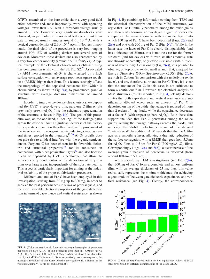
Different amounts of Par C have been employed in this
investigation, starting from 30 mg up to 300 mg, in order to
achieve the best performances in terms of process yield, and
the most favorable electrical properties of the gate dielectric
film in terms of capacitance and vertical resistance, as shown
in Fig. 4. By combining information coming from TEM and
the electrical characterization of the MIM structures, we
argue that Par C initially penetrates among the oxide grains
and then starts forming an overlayer. Figure 2 shows the
comparison between a sample with an oxide layer onto
which 150 mg of Par C have been deposited (Figs. 2(a) and
2(c)) and one with 300 mg of Par C (Fig. 2(b)). While in the
latter case the layer of Par C is clearly distinguishable (and
has a thickness of 25 nm), this is not the case for the former
structure (and for devices with even smaller amounts, data
not shown): apparently, only oxide is visible (with a thick-
ness of about 6 nm). Occasionally (Fig. 2(c)), it is possible to
observe, on top of the oxide, small islands that, analyzed by
Energy Dispersive X-Ray Spectroscopy (EDX) (Fig. 2(d)),
are rich in Carbon (in comparison with the underlying oxide
layer), and are, therefore, attributed to Par C. Thus, it is clear
that the amount of Par C, in this case, is not sufficient to
form a continuous film. However, the electrical analysis of
MIM structures (results reported in Fig. 4), clearly demon-
strates that both capacitance and vertical resistance are sig-
nificantly affected when such an amount of Par C is
deposited on top of the oxide: the leakage is reduced of more
than 2 orders of magnitude, while the capacitance decreases
of a factor 5 (with respect to bare Al2O3). Both these data
support the idea that Par C penetrates among the oxide
grains, sealing the leakage pathways across the oxide, and
reducing the global dielectric constant of the derived
“metamaterial”. In addition, AFM reveals that the Par C film
acts as a smoothing layer, allowing a dramatic reduction of
the surface corrugation, with a RMSR that goes from 5.5 nm
for Al2O3 films to 1.3 nm for Par C (300 mg)/Al2O3 films.
Correspondingly (Figs. 3(a) and 3(b)), a clear increase of the
average grain dimension of pentacene is observed (from
around 100 nm to 500 nm).
We observed, by TEM investigations (see Fig. 2(b)),
that 300 mg of Par C form a complete and almost uniform
film, with an average thickness of 25 nm; thus, this value
realistically represents the minimum thickness for achieving
a good trade-off between gate dielectric capacitance and ver-
tical resistance (see Fig. 4). Clearly, the correspondence
FIG. 4. (Color online) Vertical resistance and capacitance values of MIM
structures based on different combinations of Par C and Al2O3
FIG. 3. (Color online) Atomic force microscopy micrographs of pentacene
deposited on bare Al2O3 (a) and pentacene deposited on (300 mg) Par C/
Al2O3 (b). Al2O3 and (300 mg) Par C/Al2O3 (data not shown) are character-
ized by a RMSR of 5.5 nm and 1.3 nm, respectively. As a consequence, the
average dimensions of pentacene domains are significantly different in the
two cases, namely 100 nm (a) and 500 nm (b).
093305-3 Cosseddu et al. Appl. Phys. Lett. 100, 093305 (2012)
Downloaded 01 Mar 2012 to 77.118.13.252. Redistribution subject to AIP license or copyright; see http://apl.aip.org/about/rights_and_permissions

between the amount of dimer and the thickness of the film
depends on the features of the CVD chamber and a calibra-
tion should be done for each coating equipment. The electri-
cal characterization of OTFTs fabricated using this
technique showed a dramatic improvement of all the most
meaningful parameters. First of all, as can be noticed from
Figs. 5(a) and 5(b), the fabricated devices show a maximum
mobility around 6� 10�2 cm2/Vs, and, most importantly can
be operated at very low voltages, as they are characterized
by a very low value of the average threshold voltage
(�0.5 V), even lower than in devices based on bare Al2O3,
despite the lower gate dielectric capacitance. This is particu-
larly important as it demonstrates that for achieving low
operating voltages, it is crucial to have a proper control of
interfacial properties of the dielectric layer, in addition to a
high value of the gate dielectric capacitance. Another impor-
tant parameter, directly linked to the quality of the dielectric/
semiconductor interface, is the subthreshold slope (S),
extracted from the transfer characteristics, from which the
maximum density of interfacial trap sites can be derived,33
NmaxSS ¼
S�logðeÞkT=q � 1
h iCi
q . In this case, we obtained an average
S of 350 mV/dec, that leads to NmaxSS ¼ 4� 1012 cm�2 eV�1
(i.e., almost two orders of magnitude lower than in devices
assembled on bare Al2O3, see Table I in SI (Ref. 29)). The
obtained S values are slightly higher compared to other cases
reported in the literature11,12,34 but, in our structures, the ca-
pacitance is almost 5 times smaller. This means that the max-
imum density of trap sites in our case is lower. Compared to
more recent results,35 S is lower, but NmaxSS is of the same
order of magnitude. Moreover, we obtained a breakdown
voltage higher than 5 MV/cm, and most importantly, a very
low leakage current density (more than 4 orders of magni-
tude smaller than in bare Al2O3 devices, i.e., around
2� 10�9 A/cm2 recorded at 0.66 MV/cm) correlated with a
remarkable increase of the process yield up to 90% (over
hundreds of fabricated devices). All devices were fabricated
on commercial PET plastic substrates employed as received.
These substrates, as shown in Fig. S4,29 are usually charac-
terized by very pronounced surface defects that can cause
severe irregularities or even breaks across the gate dielectric
leading to a failure of the device. A proper planarization pro-
cess, as suggested by Sekitani et al.34 for SAM based devi-
ces, could certainly significantly improve this yield.
A statistical analysis of the most meaningful electrical pa-
rameters is reported in Table I in the SI. It is worth noting that,
despite an improvement of one order of magnitude compared
to bare Al2O3, the achieved mobility is still smaller than the
average mobility reported in the literature for pentacene based
devices.11,12,34 As a matter of fact, pentacene growth is very
sensitive to the surface corrugation of the substrate and high
mobilities can be achieved only by employing insulating films
with an average roughness much smaller than 1 nm. Again, the
use of a planarization layer on the plastic substrate34 or the
employment of organic semiconductors that are much less sen-
sitive to the substrate corrugation36 could certainly be benefi-
cial for the device performance. It is noteworthy that when a
less substrate-sensitive semiconductor, i.e., TIPS-pentacene,
was employed, mobilities as high as 0.4 cm2/Vs were
achieved, with an average value of the subthreshold slope of
around 200 mV/dec, (with the smallest achieved value of
70 mV/dec, corresponding to NmaxSS ¼ 7.5� 1011 cm�2 eV�1).
The typical output and transfer characteristics of TIPS based
OTFTs are shown in Figs. 5(c) and 5(d).
Interestingly enough, OTFTs based on a single layer of
Par C (with the same reported amounts but without Al2O3)
have been also tentatively fabricated and tested, but working
devices were never obtained, as the leakage currents were
always too high. This is particularly important as it demon-
strates that the two single dielectric films cannot be
employed alone for the fabrication of efficient ultra-low volt-
age devices, whereas a proper combination of the two gives
rise to devices with optimal performances. In conclusion, we
have demonstrated the potentiality of a combination of a
metal oxide (namely Al2O3 but the technique may in princi-
ple be applied to any metal oxide) and of the organic
FIG. 5. (Color online) Output and trans-
fer characteristics of pentacene ((a) and
(b)) and TIPS-pentacene ((c) and (d))
OTFTs fabricated using a double layer
Par C/Al2O3. The transfer characteristics
have been recorded in the saturation re-
gime at VDS¼�1 V.
093305-4 Cosseddu et al. Appl. Phys. Lett. 100, 093305 (2012)
Downloaded 01 Mar 2012 to 77.118.13.252. Redistribution subject to AIP license or copyright; see http://apl.aip.org/about/rights_and_permissions

dielectric parylene C, for the routine realization of ultra-low
voltage organic thin film transistors. With this combination
of dielectric materials, we have obtained devices that: (a)
work with bias voltages of 1 V and have an average threshold
voltage of �0.5 V; (b) within their working voltage range do
not show any significant leakage. We have also demonstrated
that this technique is able to give rise to a process yield of
more than 90% in non-optimized conditions and, therefore,
has a very interesting potential in terms of industrial
scalability.
The authors would like to thank Beatrice Fraboni and
Silvia Milita for fruitful discussions on the results; Roberto
Balboni and Jacques Legeleux for helping with TEM/SEM
investigations. Finally, the authors acknowledge financial
support by the European Commission, under the VII FP Pro-
ject “Roboskin,” Contract Number 231500. P. Cosseddu
acknowledges Regione Autonoma della Sardegna (RAS) for
funding his research activity under the POR Sardegna FSE
2007-2013, L.R.7/2007 CRP Prot. No. 1399/207. S. Lai
acknowledges Regione Autonoma della Sardegna (RAS) for
funding his Ph.D. activity under the POR Sardegna FSE
2007-2013.
1H. Shirakawa, E. J. Louis, A. G. Mac Diarmid, C. K. Chiang, and A. J.
Heeger, J. Chem. Soc., Chem. Commun. 578 (1977).2H. Koezuka, A. Tsumura, and T. Ando, Synth. Met. 18, 699 (1983).3D. H. Kim, D. Y. Lee, H. S. Lee, W. H. Lee, Y. H. Kim, J. In Han, and K.
Cho, Adv. Mater. 19, 678 (2007).4U. Zschieschang, F. Ante, T. Yamamoto, K. Takimiya, H. Kuwabara, M.
Ikeda, T. Sekitani, T. Someya, K. Kern, and H. Klauk, Adv. Mater. 22,
982 (2010).5H. C. Yan, Z. Chen, Y. Zheng, C. E. Newman, J. Quin, F. Dolz, M. Kas-
tler, and A. Facchetti, Nature 457, 679 (2009).6R. H. Reuss, B. R. Chalamala, A. Moussessian, M. G. Kane, A. Kumar,
D. C. Zhang, J. A. Rogers, M. Hatalis, D. Temple, G. Moddel et al.,Proceedings of the IEEE 93, 1239 (2005).
7G. H. Gelinck, H. Edzer, A. Huitema, E. van Veenendaal, E. Cantatore, L.
Schrijnemakers, J. B. P. H. van der Putten, T. C. T. Geuns, M. Beenhak-
kers, J. B. Giesbers et al., Nature Mater. 3, 106 (2004).8T. Someya, Y. Kato, T. Sekitani, S. Iba, Y. Noguchi, Y. Murase, H. Kawa-
guchi, and T. Sakurai, Proc. Natl. Acad. Sci. U.S.A. 102, 12321 (2005).9M. Barbaro, A. Caboni, P. Cosseddu, G. Mattana, and A. Bonfiglio, IEEE
Trans. Inf. Technol. Biomed. 14, 758 (2010).10J. Collet, O. Tharaud, A. Chapoton, and D. Vuillaume, Appl. Phys. Lett.
76, 1941 (2000).
11M. Halik, H. Klauk, U. Zschieschang, G. Schmidt, C. Dehm, M. Schutz, S.
Maisch, F. Effenberger, M. Brunnbauer, and F. Stellacci, Nature 431, 963
(2004).12H. Klauk, U. Zschieschang, J. Pflaum, and M. Halik, Nature 445, 745
(2007).13A. Ulman, Chem. Rev. 96, 1533 (1996).14J. C. Love, L. A. Estroff, J. K. Kriebel, R. G. Nuzzo, and G. M. White-
sides, Chem. Rev. 105, 1103 (2005).15F.-C. Chen, C.-S. Chuang, Y.-S. Lin, L.-J. Kung, T.-H. Chen, and H.-P. D.
Shieh, Org. Electron. 7, 435 (2006).16W. C. Shin, H. Moon, S. Yoo, Y. Li, and B. J. Cho, IEEE Electron Device
Lett. 31, 1308 (2010).17Y.-G. Ha, J. D. Emery, M. J. Bedzyk, H. Usta, A. Facchetti, and T. J.
Marks, J. Am. Chem. Soc. 133, 10239 (2011).18M.-H. Yoon, H. Yan, A. Facchetti, and T. Marks, J. Am. Chem. Soc. 127,
10388 (2005).19X. Cheng, M. Caironi, Y.-Y. Noh, J. Wang, C. Newman, H. Yan, A. Fac-
chetti, and H. Sirringhaus, Chem. Mater. 22, 1559 (2010).20C. E. Murphy, L. Yang, S. Ray, L. Yu, S. Knox, and N. Stingelin, J. Appl.
Phys. 110, 093523 (2011).21J. H. Cho, J. Lee, Y. Xia, B. S. Kim, Y. He, M. J. Renn, T. P. Lodge, and
C. D. Frisbie, Nature Mater. 7, 900 (2008).22L. Herlogsson, M. Colle, S. Tierney, X. Crispin, and M. Berggren, Adv.
Mater. 22, 72 (2010).23M. J. Panzer and C. D. Frisbie, J. Am. Chem. Soc. 129, 6599 (2007).24L. L. Chua, J. Zaumseil, J. F. Chang, E. Ou, H. Sirringhaus, and R. H.
Friend, Nature 434, 194 (2005).25M. Kaltenbrunner, P. Stadler, R. Schwodiauer, A. W. Hassel, N. S. Sari-
ciftci, and S. Bauer, Adv. Mater. 23, 4892 (2011).26X.-D. Dang, W. Plieth, S. Richter, M. Plotner, and W.-J. Fischer, Phys.
Status Solidi A 205, 626 (2008).27A. Khabari and F. K. Urban III, J. Non-Cryst. Solids 351, 3536 (2005).28K. Crain, Surf. Mount Technol. 9, 50 (1995).29See supplementary material at http://dx.doi.org/10.1063/1.3691181 for the
electrical characterization of bare Al2O3 devices, a comparison of the
main electrical parameter in the two different configurations, and a mor-
phological investigation of the employed PET substrate.30F. D. Fleischli, S. Suarez, M. Schaer, and L. Zuppiroli, Langmuir 26,
15044 (2010).31A. Kahouli, A. Sylvestre, L. Ortega, F. Jomni, B. Yangui, M. Maillard,
B. Berge, J.-C. Robert, and J. Legrand, Appl. Phys. Lett. 94, 152901
(2009).32D. Wright, B. Rajalingam, S. Selvarasah, M. R. Dokmecid, and A. Kha-
demhosseini, Lab Chip 7, 1272 (2007).33A. Rolland, J. Richard, J. P. Kleider, and D. Mencaraglia, J. Electrochem.
Soc. 140, 3679 (1993).34T. Sekitani, U. Zschieschang, H. klauk, and T. Someya, Nature Mater. 9,
1015 (2010).35N. B. Ukah, J. Granstrom, R. R. S. Gari, G. M. King, and S. Guha, Appl.
Phys. Lett. 99, 243302 (2011).36U. Zschieschang, T. Yamamoto, K. Takimiya, H. Kuwabara, M. Ikeda, T.
Sekitani, T. Someya, and H. Klauk, Adv. Mater. 23, 654 (2011).
093305-5 Cosseddu et al. Appl. Phys. Lett. 100, 093305 (2012)
Downloaded 01 Mar 2012 to 77.118.13.252. Redistribution subject to AIP license or copyright; see http://apl.aip.org/about/rights_and_permissions


