Embed Size (px)
Citation preview

Ue
Ka
b
a
ARRAA
KETA
1
ioticat[
af[aamimo
0d
Electrochimica Acta 69 (2012) 320– 327
Contents lists available at SciVerse ScienceDirect
Electrochimica Acta
j ourna l ho me pag e: www.elsev ier .com/ locate /e lec tac ta
se of a plating additive to enable continuous metallization of nanoscalelectrochemically patterned chemical templates
yle A. Nelsona, Matthew R. Linfordb, Dean R. Wheelera, John N. Harba,∗
Department of Chemical Engineering, Brigham Young University, Provo, UT 84602 United StatesDepartment of Chemistry and Biochemistry, Brigham Young University, Provo, UT 84602 United States
r t i c l e i n f o
rticle history:eceived 5 December 2011eceived in revised form 2 March 2012ccepted 2 March 2012vailable online 13 March 2012
eywords:lectroless plating additive
a b s t r a c t
This paper examines the use of amine-functionalized templates to create nanopatterned metal fea-tures. A key aspect of the work is the use of an additive to increase the plating density and enablecontinuous metallization of nanoscale features. Specifically, MPS (3-mercapto-1-propane sulfonate) wasfound to increase the plating density of copper on amine-functionalized surfaces by attaching to thesurface via the sulfonic acid group, leaving the thiol free to attract palladium ions to the surface. Amine-functionalized nanotemplates were made by selective deposition of PAAm onto surface patterns createdby nano-oxidation of OTS-coated silicon substrates. Selective, continuous metallization was observed
emplated copper depositionFM nano-oxidation
for MPS-treated nanotemplates. These results demonstrate the successful creation of flexible amine-functionalized nanotemplates, and the enabling influence of MPS for the metallization of nanometer-scalefeatures. In particular, MPS was found to reduce the pattern width for feasible metallization from 500 nmto less than 100 nm. While the PAAm templates were used in this paper to demonstrate selective met-allization, they have the potential for broad application in areas such as selective surface attachment ofbiomolecules to nanometer-scale surface features.
© 2012 Elsevier Ltd. All rights reserved.
. Introduction
Selective placement of nanomaterials on surfaces is a challeng-ng aspect of nanoscience. One way to selectively place a materialn a surface is to pattern the surface with specific chemical groupshat have an affinity for the material of interest. This type of pattern-ng is generally referred to as chemical templating, and stands inontrast to traditional masking techniques. Chemically templatedmines are of particular interest and have been used for the selec-ive attachment of palladium for catalyzing surface metallization1–5], gold nanoparticles [6], proteins [7], and DNA [7–10].
For palladium-catalyzed metallization of insulating surfaces,mine containing silane monolayers can be used to prepare a sur-ace for palladium attachment prior to electroless metallization3,11,12]. Palladium is often used as a seed metal because of itsbility to facilitate the electroless deposition of a variety of met-ls [13]. Chemical templating of amines for palladium-catalyzedetallization has been demonstrated with photolithographic mod-
fication of silane monolayers [8,10,14] and nanografting of silaneonolayers [1]. It appears, however, that both of these meth-
ds were limited to feature sizes greater than 200 nm. Amine
∗ Corresponding author.E-mail address: john [email protected] (J.N. Harb).
013-4686/$ – see front matter © 2012 Elsevier Ltd. All rights reserved.oi:10.1016/j.electacta.2012.03.016
templates with feature sizes less than 100 nm have been fabri-cated by the deposition of APTES (3-aminopropyl-triexthoxysilane,NH2CH2CH2CH2Si(OCH2CH3)3) onto patterns created by AFM tip-directed nano-oxidation [8], but these templates have not beenused for metallization [15]. Patterned amine templates with featuresizes less than 100 nm were also created with use of hierarchi-cally assembled organic bilayers, and subsequently used for theattachment of gold nanoparticles [6].
As template size drops to length scales below 100 nm, thedensity of nucleation sites becomes increasingly important. Theminimum size of the continuous metallized pattern that can beformed is directly related to the maximum distance between seeds.As displayed in, Fig. 1, the distance between seeds affects how largeeach particle must grow to form a continuous feature. While seedsmay not necessarily be evenly spaced, an increase in the density ofseeds on a template allows for continuous features with a smallerpossible width.
This work is one of two papers studying the effect of additiveson nanoscale deposition of metals on insulating substrates. Thecompanion paper [16] describes a procedure developed to increasepalladium seed density on unpatterned silicon oxide surfaces cov-
ered with APTES monolayers by pretreating the surfaces with MPS(3-mercaptopropylsulfonic acid sodium salt, HSCH2CH2CH2SO3Na)and other additives. The present study is intended to test thehypothesis that an increase in seed density by MPS treatment may
K.A. Nelson et al. / Electrochimica
Fig. 1. Idealization of nucleation sites, n and n , of higher (a) and lower (b) lineardw
ecauattlrpw
2
2
o(p9cprtwvmo
a0
Ff
a b
ensity with subsequent metallization, ma and mb, and minimum feature widths,a and wb, respectively, for continuous metallization.
nable continuous metallization of palladium seeded amine-basedhemical templates at a smaller scale compared to metallization ofmine-based templates alone. In particular, this work examines these of AFM tip-directed nano-oxidation to create finely patternedmine-templated surfaces, and the use of an additive to enable con-inuous copper metallization of those templates. The interaction ofhe MPS additive with amine-coated surfaces and its effect on pal-adium ion adsorption is investigated in order to understand theole of the additive in enhancing metallization. A new patterningrocedure that utilizes a polymer to create amine nanotemplatesith enhanced selectivity is also demonstrated.
. Experimental
.1. APTES surface preparation
Substrates were Si(1 0 0) wafers covered with a ca. 2 nm nativexide. Si(1 0 0) shards (∼1 cm2) were cleaned in a plasma reactorHarrick Plasma, PDC-32G) on the high setting for 30 s and thenlaced in a vacuum oven at −10 psig and 150 ◦C. APTES (Aldrich9%) was then injected into the oven yielding a vapor phase con-entration of 1.2 × 10⁻⁴ mol/L. The samples were exposed to vaporhase APTES for 30 min to form an APTES layer on the surface. Theesulting monolayer was 0.9 nm thick by spectroscopic ellipsome-ry (J.A. Woollam Co., Inc., Model M2000D) and had an advancingater contact angle of 55◦ (Ramé-Hart Inc., Model 100-00). These
alues are in reasonable agreement with literature values for APTESonolayers on silicon oxide surfaces and suggest a small amount
f water was present in the deposition system [17–20].After APTES deposition, samples were treated, metallized and/or
nalyzed immediately. APTES-coated samples were immersed in.1 M aqueous MPS or PDS for 1 h, rinsed with water for 5 s,
ig. 2. SEM images of (a) an APTES-coated surface and (b) a MPS treated APTES-coated surfor 20 s. The scale bar denotes 2 �m.
Acta 69 (2012) 320– 327 321
and dried with a clean nitrogen stream. Samples were analyzedfor changes in surface chemistry by XPS (Surface Science SSX-100 instrument with a monochromatized Al K� source and ahemispherical analyzer). Nitrogen and sulfur peaks are relativelylow-signal peaks, so varying amounts of noise were present evenafter very long scan times. All water used in this study was 18.2 M�resistivity deionized water obtained from a Millipore Milli-Q filter.
2.2. Metallization procedures
Surfaces were seeded by immersion for 15 min in a PdCl2 and HClsolution (0.15–0.2 g dm−1 PdCl2, pH 3.5), followed by a 30 s dip in0.1 M aqueous NaBH4; samples were rinsed with water and dried ina nitrogen stream after each step. The surfaces were subsequentlyplated with copper by immersing them in an electroless copperplating solution (0.06 M CuSO4; 0.5 M NaOH; 0.25 M Rochelle Salt;0.12 M formaldehyde), rinsed with water, and dried in a clean nitro-gen stream (plating time is specified for each image set).
2.3. Surface preparation and treatments for nano-oxidation
Si(1 0 0) surfaces were cleaned in a plasma reactor (Harrick PDC-32G) on the high setting for 30 s and then twice immersed in a5 mM solution of OTS (Gelest, 95%) in dicyclohexyl (Aldrich, 99%)for 30 s and rinsed with toluene [21]. The resulting monolayer was1.3 nm thick by ellipsometry and had an advancing water con-tact angle of 100◦, characteristic of a dense though not completemonolayer. AFM tip-directed nano-oxidation was performed usinga Dimension V AFM (Veeco) and platinum-coated AFM tips (DPER14, MikroMasch). Features were oxidized locally at an appliedpotential between −10 and −11 V at a tip speed of 5.0–5.1 �m/s.Nano-oxidized surfaces were immersed in an aqueous solutionof 0.2 wt% PAAm (Sigma, 17,000 MW, 20% aq) and 15–20% CTAC(cetyltrimethylammonium chloride, sigma, 25% aq) [7]. These sur-faces were then treated with MPS and/or metallized as indicatedabove.
3. Results and discussion
3.1. Increased metallization by MPS treatment
Prior to evaluation of the effect of additive treatment on themetallization of nanoscale amine-based chemical templates, the
influence of MPS on the electroless copper metallization of APTES-coated surfaces was examined. A comparison of APTES-coatedsurfaces with and without pretreatment with MPS (prior to seed-ing) shows that the addition of MPS resulted in a significant increaseace that have been seeded with Pd, reduced, and plated by electroless Cu deposition

322 K.A. Nelson et al. / Electrochimica Acta 69 (2012) 320– 327
Table 1Pd/N Ratios obtained by XPS of seeded surfaces before the reduction step. Errors arestandard deviations of XPS measurements (N = 8).
Surface Average Pd/N ratio
APTES 0.42 ± 0.01
isPocmshpe
3
bpthpwrstPTbpott
tPwoXwgTpobtpstatMfntwn
fs
Fig. 3. Nitrogen 1s XPS spectra of differently treated APTES surfaces, (a) APTES with-
amine functionalized surface, where each end bound to the surfaceprovides one sulfur per amine. In addition, the PDS molecule blocksattachment sites as it lays on the surface, leading to the observed
APTES + PDS 0.36 ± 0.03APTES + MPS 0.73 ± 0.10
n the density of electroless copper metallization. These results areimilar to those reported for the electroless deposition of Pd ond-seeded surfaces [16]. Fig. 2 displays a side-by-side comparisonf samples seeded with palladium and immersed in an electrolessopper bath for 20 s. The MPS pretreated surface is more uniformlyetallized than the untreated surface, suggesting better disper-
ion of nucleation sites, smaller size distribution of seeds, and/origher seed density. The impact of this additive on electroless cop-er deposition shows that the effects of MPS are not limited tolectroless palladium metallization.
.2. Determination of mechanism for enhanced metallization
Experiments were performed to determine the mechanismy which the MPS led to an increase in plating density. X-rayhotoelectron spectroscopy (XPS) was used to measure the quan-ity of nitrogen and palladium on APTES-coated surfaces thatad been seeded with and without MPS pretreatment. PDS (1,3-ropanedisulfonic acid disodium salt, NaO3SCH2CH2CH2SO3Na)as used as a comparison to MPS to help understand the specific
ole of the two functional groups of MPS in enhancing seeding. Thetructure of these two additives is similar except that MPS has ahiol group at one end and a sulfonic acid group at the other, whileDS has two sulfonic acid groups, one at either end of the molecule.he XPS results in Table 1 show that seeding of a surface that hadeen pretreated with MPS results in a 74% increase in the ratio ofalladium to nitrogen (Pd/N ratio, atom%) relative to the Pd/N ratiof a seeded APTES surface that had no additive treatment. In con-rast, pretreatment with PDS appeared to reduce the Pd/N ratio onhe surface.
XPS was also used to characterize the chemical interactions ofhe additives with the APTES monolayer prior to exposure to thed solution. Comparison of the results for MPS-pretreated surfacesith those pretreated with PDS permitted assessment of the effect
f the two different chemical groups on seeding and metallization.PS revealed that the nitrogen peak obtained from an APTES surfaceas present primarily as a single peak (Fig. 3a), while the nitro-
en peak of the MPS-pretreated APTES surfaces was split (Fig. 3b).he same peak splitting was observed in the analysis of the PDS-retreated APTES surface (Fig. 3c). The peak splitting (the presencef more than one chemical state) is indicative of an interactionetween the additives and the amine groups on the surface. Ashe interaction is similar for both additives, and the only groupsresent on the PDS for potential interaction with the surface areulfonic acid groups, it follows the interaction of the additive withhe surface for both MPS and PDS is primarily through the sulfoniccid group. The most likely interaction is an ionic bond betweenhe protonated amine and the deprotonated sulfonic acid. Thus, for
PS, the sulfonate binds ionically with the amine, and the thiol wasree to bind PdCl4−2 ions. The 2 eV shift in the binding energy of theitrogen causing the peak split is consistent with that expected forhe proposed attachment mechanism [22]. In contrast, a larger shiftould have been expected for a change in the oxidation state of the
itrogen (a minimum of 4 eV for oxidation of amines) [23].The XPS results for sulfur (Fig. 4) showed two oxidation statesor the MPS-treated surface (one for the sulfhydyl and one for theulfonic acid in two peaks of ca. equal area), and one oxidation
out additive treatment, (b) MPS-treated APTES, and (c) PDSA-treated APTES. Thepeak split is caused by the ionic bonding of sulfonic acid groups with the primaryamines of the APTES monolayers.
state for the PDS-treated surface (corresponding to a sulfonic acidgroup). The sulfur to nitrogen (S/N) ratios from the XPS data forMPS and PDS were 1.9 and 0.3, respectively. The ratio for MPS (1.9)is consistent with high surface coverage and two sulfurs per amine,one sulfur associated with the sulfonic acid group that attaches tothe amine, and the other with the thiol on the opposite end. Whilea palladium ion may interact with more than one amine on thesurface [24,25], only one thiol is likely needed in order to bind apalladium ion [12,26]. The low S/N ratio for PDS treated is believedto be the result of both ends of the molecule interacting with the
Fig. 4. Sulfur [2s] signal peaks of (a) MPS and (b) PDSA treated APTES surfaces. Asexpected, the sulfur peak of the MPS treated surface is split (with the sulfhydrylat 228 eV and the sulfonic acid at 233 eV) and the sulfur peak of the PDSA treatedsurface was present only in its more oxidized/higher binding energy state.

K.A. Nelson et al. / Electrochimica Acta 69 (2012) 320– 327 323
electi
l(iatAwrwisi3p
3
pscebppoFdstn(oos
Fd
results for a series of lines of different widths, both with and with-out MPS treatment. Without MPS only sparse metallization wasobserved for line widths below 400 nm. In contrast, samples treatedwith MPS showed nearly continuous metallization for the entire
Fig. 5. Schematic diagram of a stepwise process for s
ow S/N ratio of 0.3. The S/N ratios dropped to 0.6 (MPS) and 0.2PDS), respectively, when the surface was seeded with palladium,ndicating that adsorbed palladium ions compete with the sulfoniccid groups for interaction with the amines. The presence of PDS onhe surface led to a Pd/N ratio that was lower than that observed forPTES alone, as the sulfonic acid groups do not interact significantlyith palladium ions in acidic HCl solutions [27]. The addition of MPS
esulted in a significantly higher Pd/N ratio (0.73) relative to APTES,hich resulted in an increase in copper plating density (Fig. 2) and
s expected to improve the nucleation density of nano-patternedurface features. The measured MPS S/N ratio of 0.6 after treatmentn the palladium solution (approximately 1 MPS molecule to every
amines) indicates that both thiols and the amines play a role inalladium ion adsorption.
.3. Development of an amine template
Having established the effectiveness of MPS for improving thelating density of copper metallization by increased palladiumeeding on APTES-coated surfaces, the ability of MPS to enhanceopper metallization of amine-templated nano-scale patterns wasxplored. Nanoscale amine-functionalized templates were formedy the process illustrated in Fig. 5. First, a native oxide surface wasassivated with an octadecyltrichlorosilane (OTS) monolayer. Theassivated surface was then patterned by AFM tip-directed nano-xidation to form a fresh raised oxide in the pattern of interest.inally, an amine-functionalized polymer, PAAm, was selectivelyeposited on the patterned areas as had been previously demon-trated for much larger patterns [2]. An attempt was also madeo attach APTES directly to the oxide surface patterns; unfortu-ately, this resulted in a high level of non-selective metallizationsee, e.g., Fig. 6). While metallization of the patterned lines was
bserved, the high level of background metallization (even with-ut MPS treatment) precluded its use for nanopatterning in thistudy.ig. 6. SEM images of metalized APTES treated surface patterns. The electrolesseposition time was 2 min and the scale bar denotes 2 �m.
ve surface patterning of PAAm on alkyl monolayers.
After PAAm deposition, the resulting surface was seeded bothwith and without MPS treatment. Height measurements followingoxidation, polymer deposition, and seeding with Pd are shown inFig. 7. The height increase of patterned regions after PAAm treat-ment was 4 A. While this height is lower than the reported thicknessof PAAm deposited on clean oxide for this PAAm/CTAT solution [2],it is is reasonable to expect that PAAm may deposit differently onthese patterns as nano-oxidation may not provide a surface of thesame quality. The measured height change was consistent for 60patterned lines on two different surfaces, suggesting depositionof ca. a single monolayer of PAAm. In the PAAm/CTAC solution,CTAC significantly decreases the amount of PAAm that sticks tohydrophobic surfaces. While decreasing the percent CTAC in thissolution may have allowed more PAAm to deposit on the oxidepatterns, it would also have increased non-specific adsorption ofPAAm [2].
3.4. Effects of MPS treatment on metallization of amine templates
Once seeded, samples were metallized by plating with electro-less copper for 2 min. Fig. 8 shows a comparison of metallization
Fig. 7. AFM tapping mode height images of lines patterned after (a) AFM tip-directednano-oxidation, (b) with attachment of PAAm, and (c) after Pd seeding of the lines.The scale bar denotes 1 �m.

324 K.A. Nelson et al. / Electrochimica Acta 69 (2012) 320– 327
Fig. 8. SEM images of metalized, patterned PAAm nanotemplates showing varying line widths (a) without MPS treatment and (b) with MPS treatment. Line widths for (a)and (b) from top to bottom are 400, 300, 200, 100, and 80 nm (two lines). Each surface was immersed in an electroless copper plating bath for 2 min. The patterned lines are5 �m long.
F reatmw 5 �m l
rmaw
a
Fp
ig. 9. SEM images of metalized, patterned PAAm nanotemplates (a) without MPS tas immersed in the electroless copper solution for 2 min. The patterned lines are
ange of line widths considered. The effect of MPS on increasedetallization of the templates is clear. MPS treatment enabled met-
llization of surface patterns 5 times smaller than those patterned
ith PAAm alone.A comparison of patterned lines smaller than 100 nm shows distinct contrast in metallization with the use of MPS (see
ig. 10. SEM of OTS surfaces (a) treated with 15% aqueous CTAC, seeded, and plated (b) trlated. The electroless deposition time was 2 min and the scale bar denotes 2 �m.
ent and (b) with MPS treatment. Pattern widths are all under 100 nm. Each surfaceong.
Fig. 9). Without MPS treatment, no appreciable metal depositionwas observed. In contrast, continuous, selective metallization wasobserved for samples treated with MPS (Fig. 9b). As discussed
previously, both the amine and thiol groups have a role in the seed-ing process. In the discussion of Fig. 7, it is noted that, even onthe smallest patterns, the observed height increase at each stepeated with PAAm, seeded, and plated and (c) treated with PAAm, MPS, seeded, and

K.A. Nelson et al. / Electrochimica Acta 69 (2012) 320– 327 325
lated P
ifampt
sms((sw1
Fig. 11. Stepwise metallization on temp
ndicates polymer deposition and palladium attachment. There-ore, the smallest patterns appear to have templated amines thatre expected to attract palladium. However, without MPS treat-ent no notable electroless metallization was observed. It is
ossible that MPS was needed in order to attract enough palladiumo reach a critical seed size in order for deposition to occur.
While the use of PAAm was an improvement over the non-pecific metallization seen with the use of APTES, some non-specificetallization was still seen on PAAm treated OTS monolayer coated
urfaces. To determine the cause of this background depositionsee Figs. 8 and 9), OTS monolayers were treated with CTAC
cetyltrimethylammonium chloride), PAAm, and/or MPS, and sub-equently metallized (Fig. 10). No significant metal depositionas observed on OTS monolayers that had been treated with a5% aqueous CTAC solution (the PAAm solution without PAAm,
AAm with and without MPS treatment.
see Fig. 10a). Surfaces treated with PAAm/CTAC before metaldeposition (shown in Fig. 10b) consistently displayed some back-ground deposition, indicating that non-specific adsorption of PAAmwas the main contributor to non-selective metallization on thesurfaces. As MPS treatment enhanced the metallization of PAAmtemplates, it also enhanced the metallization of non-specificallyadsorbed PAAm.
A comparison of the process for metallization of MPS-treatedand untreated PAAm templates is summarized in Fig. 11. The addi-tive clearly had a significant impact on the nanodeposition ofcopper, especially for the smallest line sizes where no clear evi-
dence of plating was observed without the additive (see Fig. 9).While the principal results of this paper were illustrated bypatterning lines, the method is by no means restricted to that geom-etry. For example, the method was used to create the “complex”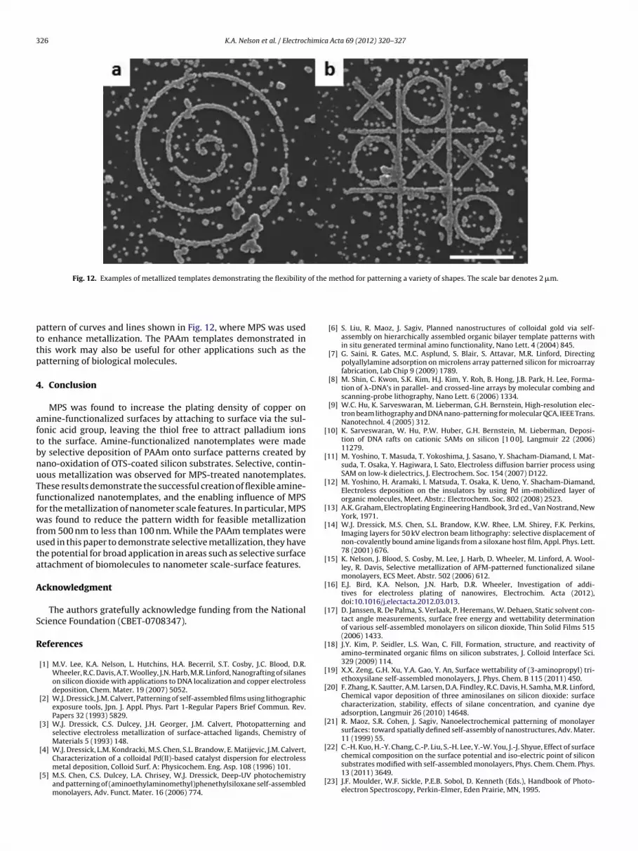
326 K.A. Nelson et al. / Electrochimica Acta 69 (2012) 320– 327
Fig. 12. Examples of metallized templates demonstrating the flexibility of the method for patterning a variety of shapes. The scale bar denotes 2 �m.
pttp
4
aftbnuTffwfuta
A
S
R
[
[
[
[
[
[
[
[
[
[
[
[
[
attern of curves and lines shown in Fig. 12, where MPS was usedo enhance metallization. The PAAm templates demonstrated inhis work may also be useful for other applications such as theatterning of biological molecules.
. Conclusion
MPS was found to increase the plating density of copper onmine-functionalized surfaces by attaching to surface via the sul-onic acid group, leaving the thiol free to attract palladium ionso the surface. Amine-functionalized nanotemplates were madey selective deposition of PAAm onto surface patterns created byano-oxidation of OTS-coated silicon substrates. Selective, contin-ous metallization was observed for MPS-treated nanotemplates.hese results demonstrate the successful creation of flexible amine-unctionalized nanotemplates, and the enabling influence of MPSor the metallization of nanometer scale features. In particular, MPSas found to reduce the pattern width for feasible metallization
rom 500 nm to less than 100 nm. While the PAAm templates weresed in this paper to demonstrate selective metallization, they havehe potential for broad application in areas such as selective surfacettachment of biomolecules to nanometer scale-surface features.
cknowledgment
The authors gratefully acknowledge funding from the Nationalcience Foundation (CBET-0708347).
eferences
[1] M.V. Lee, K.A. Nelson, L. Hutchins, H.A. Becerril, S.T. Cosby, J.C. Blood, D.R.Wheeler, R.C. Davis, A.T. Woolley, J.N. Harb, M.R. Linford, Nanografting of silaneson silicon dioxide with applications to DNA localization and copper electrolessdeposition, Chem. Mater. 19 (2007) 5052.
[2] W.J. Dressick, J.M. Calvert, Patterning of self-assembled films using lithographicexposure tools, Jpn. J. Appl. Phys. Part 1-Regular Papers Brief Commun. Rev.Papers 32 (1993) 5829.
[3] W.J. Dressick, C.S. Dulcey, J.H. Georger, J.M. Calvert, Photopatterning andselective electroless metallization of surface-attached ligands, Chemistry ofMaterials 5 (1993) 148.
[4] W.J. Dressick, L.M. Kondracki, M.S. Chen, S.L. Brandow, E. Matijevic, J.M. Calvert,
Characterization of a colloidal Pd(II)-based catalyst dispersion for electrolessmetal deposition, Colloid Surf. A: Physicochem. Eng. Asp. 108 (1996) 101.[5] M.S. Chen, C.S. Dulcey, L.A. Chrisey, W.J. Dressick, Deep-UV photochemistryand patterning of (aminoethylaminomethyl)phenethylsiloxane self-assembledmonolayers, Adv. Funct. Mater. 16 (2006) 774.
[
[6] S. Liu, R. Maoz, J. Sagiv, Planned nanostructures of colloidal gold via self-assembly on hierarchically assembled organic bilayer template patterns within situ generated terminal amino functionality, Nano Lett. 4 (2004) 845.
[7] G. Saini, R. Gates, M.C. Asplund, S. Blair, S. Attavar, M.R. Linford, Directingpolyallylamine adsorption on microlens array patterned silicon for microarrayfabrication, Lab Chip 9 (2009) 1789.
[8] M. Shin, C. Kwon, S.K. Kim, H.J. Kim, Y. Roh, B. Hong, J.B. Park, H. Lee, Forma-tion of �-DNA’s in parallel- and crossed-line arrays by molecular combing andscanning-probe lithography, Nano Lett. 6 (2006) 1334.
[9] W.C. Hu, K. Sarveswaran, M. Lieberman, G.H. Bernstein, High-resolution elec-tron beam lithography and DNA nano-patterning for molecular QCA, IEEE Trans.Nanotechnol. 4 (2005) 312.
10] K. Sarveswaran, W. Hu, P.W. Huber, G.H. Bernstein, M. Lieberman, Deposi-tion of DNA rafts on cationic SAMs on silicon [1 0 0], Langmuir 22 (2006)11279.
11] M. Yoshino, T. Masuda, T. Yokoshima, J. Sasano, Y. Shacham-Diamand, I. Mat-suda, T. Osaka, Y. Hagiwara, I. Sato, Electroless diffusion barrier process usingSAM on low-k dielectrics, J. Electrochem. Soc. 154 (2007) D122.
12] M. Yoshino, H. Aramaki, I. Matsuda, T. Osaka, K. Ueno, Y. Shacham-Diamand,Electroless deposition on the insulators by using Pd im-mobilized layer oforganic molecules, Meet. Abstr.: Electrochem. Soc. 802 (2008) 2523.
13] A.K. Graham, Electroplating Engineering Handbook, 3rd ed., Van Nostrand, NewYork, 1971.
14] W.J. Dressick, M.S. Chen, S.L. Brandow, K.W. Rhee, L.M. Shirey, F.K. Perkins,Imaging layers for 50 kV electron beam lithography: selective displacement ofnon-covalently bound amine ligands from a siloxane host film, Appl. Phys. Lett.78 (2001) 676.
15] K. Nelson, J. Blood, S. Cosby, M. Lee, J. Harb, D. Wheeler, M. Linford, A. Wool-ley, R. Davis, Selective metallization of AFM-patterned functionalized silanemonolayers, ECS Meet. Abstr. 502 (2006) 612.
16] E.J. Bird, K.A. Nelson, J.N. Harb, D.R. Wheeler, Investigation of addi-tives for electroless plating of nanowires, Electrochim. Acta (2012),doi:10.1016/j.electacta.2012.03.013.
17] D. Janssen, R. De Palma, S. Verlaak, P. Heremans, W. Dehaen, Static solvent con-tact angle measurements, surface free energy and wettability determinationof various self-assembled monolayers on silicon dioxide, Thin Solid Films 515(2006) 1433.
18] J.Y. Kim, P. Seidler, L.S. Wan, C. Fill, Formation, structure, and reactivity ofamino-terminated organic films on silicon substrates, J. Colloid Interface Sci.329 (2009) 114.
19] X.X. Zeng, G.H. Xu, Y.A. Gao, Y. An, Surface wettability of (3-aminopropyl) tri-ethoxysilane self-assembled monolayers, J. Phys. Chem. B 115 (2011) 450.
20] F. Zhang, K. Sautter, A.M. Larsen, D.A. Findley, R.C. Davis, H. Samha, M.R. Linford,Chemical vapor deposition of three aminosilanes on silicon dioxide: surfacecharacterization, stability, effects of silane concentration, and cyanine dyeadsorption, Langmuir 26 (2010) 14648.
21] R. Maoz, S.R. Cohen, J. Sagiv, Nanoelectrochemical patterning of monolayersurfaces: toward spatially defined self-assembly of nanostructures, Adv. Mater.11 (1999) 55.
22] C.-H. Kuo, H.-Y. Chang, C.-P. Liu, S.-H. Lee, Y.-W. You, J.-J. Shyue, Effect of surface
chemical composition on the surface potential and iso-electric point of siliconsubstrates modified with self-assembled monolayers, Phys. Chem. Chem. Phys.13 (2011) 3649.23] J.F. Moulder, W.F. Sickle, P.E.B. Sobol, D. Kenneth (Eds.), Handbook of Photo-electron Spectroscopy, Perkin-Elmer, Eden Prairie, MN, 1995.

himica
[
[
[26] L. Xu, J. Liao, L. Huang, N. Gu, H. Zhang, J. Liu, Pendant thiol groups-attached
K.A. Nelson et al. / Electroc
24] H. Dai, H. Li, F. Wang, Electroless Ni–P coating preparation of conductive
mica powder by a modified activation process, Appl. Surf. Sci. 253 (2006)2474.25] K. Tanaka, M. Shionoya, Synthesis of a novel nucleoside for alternativeDNA base pairing through metal complexation, J. Org. Chem. 64 (1999)5002.
[
Acta 69 (2012) 320– 327 327
Pd(II) for initiating metal deposition, Appl. Surf. Sci. 211 (2003) 184.27] S. Åkerfeldt, G. Lövgren, Spectrophotometric determination of disulfides,
sulfinic acids, thio ethers, and thiols with the palladium (II) ion, Anal. Biochem.8 (1964) 223.


