Embed Size (px)
Citation preview
UNIVERSITY OF TEXAS AT DALLAS
Project ReportEECT6325: VLSI DESIGN
Programmable PWM Controller
Guided By: Dr. Poras T. Balsara
Associate Dean for Academic AffairsProfessor of Electrical Engineering
Error! No text of specified style in document. Error! No text of specified style in document.
Error! Use the Home tab to apply Proc number to the text that you want to appear here. Error! No text of specified style in document.
Prepared By: Aalay D. Kapadia
Group No. 5 (2021199749)
Error! No text of specified style in document. Error! No text of specified style in document. Page 2 of 74PP157T-xx Concept Assessment Report
Error! No text of specified style in document. Date of last revision: Error! No text of specified style in document.This document is uncontrolled when printed. See ARTC Intranet for latest version. Version Error! No text of specifiedstyle in document.
Group No. 5 (2021199749)26 October 2022
AcknowledgementI would like to acknowledge and extend my
heartfelt gratitude to following persons who made
the completion of this project and report
possible: Dr. Poras Balsara & VLSI subject
teaching assistant Mr. Prashant Buck for their
invaluable technical support and guidance
throughout the completion of this Project.
-Aalay Kapadia
Page 3 of 74
Group No. 5 (2021199749)26 October 2022
AbstractPulse Width Modulation(PWM) circuits are used in
several applications; include DC-DC converters
wherein they are used to control one or two
switches (S1 and S2) to regulate output voltage or
current. The PWM controller for this project is
expected to produce two outputs, S1 and S2 each
capable of producing up to 1 MHz (i.e., Ts=1μs)
PWM signal for trailing-edge modulation (TEM) or
leading-edge modulation (LEM). PWM controller
which can be programmed by providing duty cycle
(D), dead-time (dt), and mode (TEM or LEM). After
finalizing your design schematics draw a DRC clean
layout for your project, extract the SPICE netlist
Page 4 of 74
Group No. 5 (2021199749)26 October 2022
and simulate it thoroughly for speed and power
dissipation.
Content Acknowledgment
Abstract
Chapter 1 System level design (Architecture)1.1 Block Diagram
Page 5 of 74
Group No. 5 (2021199749)26 October 2022
1.2 Circuit Design Description
Chapter 2 Basic Circuit design details2.1 NAND gate
2.2 NOR gate
2.3 XOR gate
2.4 D Flip Flop
2.5 SR Latch
2.6 T Flip Flop
2.7 Half adder
2.8 Full adder
2.9 Multiplexor
2.10 Summary
Chapter 3 Chip Design3.1 Complete circuit schematic design
3.2 Complete circuit Layout
3.3 Layout Design summary
Chapter 4 Complete Functional Simulation4.1 TEM MODE OPERATION SIMULATIONS
4.2 LEM MODE OPERATION SIMULATIONS
Chapter 5 Conclusion and Summary
Chapter 6 References
Appendix
Page 6 of 74
Group No. 5 (2021199749)26 October 2022
Chapter 1
System Level Design
(Architecture):
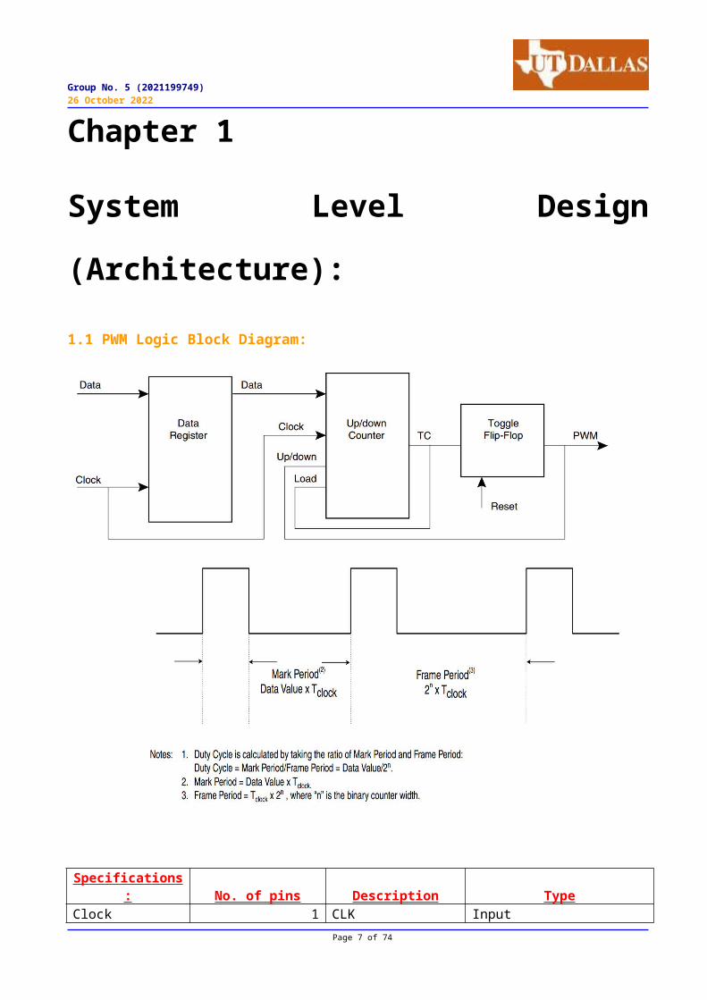
1.1 PWM Logic Block Diagram:
Specifications: No. of pins Description Type
Clock 1 CLK InputPage 7 of 74
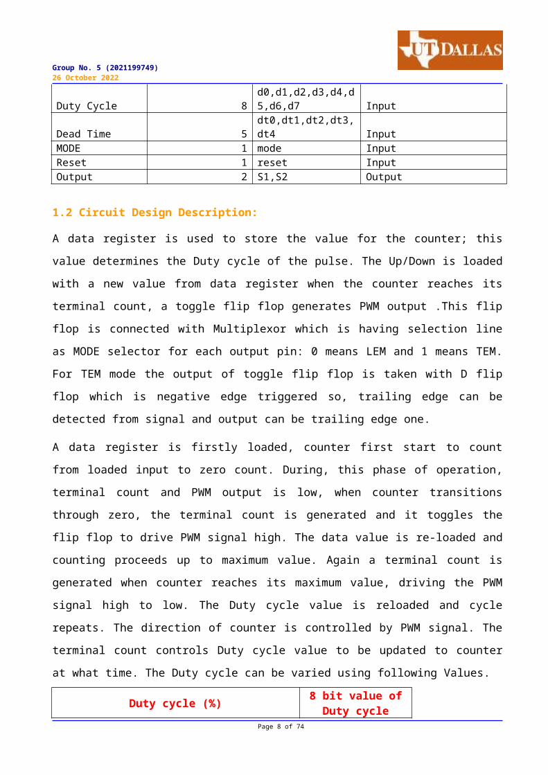
Group No. 5 (2021199749)26 October 2022
Duty Cycle 8d0,d1,d2,d3,d4,d5,d6,d7 Input
Dead Time 5dt0,dt1,dt2,dt3,dt4 Input
MODE 1 mode InputReset 1 reset InputOutput 2 S1,S2 Output
1.2 Circuit Design Description:
A data register is used to store the value for the counter; this
value determines the Duty cycle of the pulse. The Up/Down is loaded
with a new value from data register when the counter reaches its
terminal count, a toggle flip flop generates PWM output .This flip
flop is connected with Multiplexor which is having selection line
as MODE selector for each output pin: 0 means LEM and 1 means TEM.
For TEM mode the output of toggle flip flop is taken with D flip
flop which is negative edge triggered so, trailing edge can be
detected from signal and output can be trailing edge one.
A data register is firstly loaded, counter first start to count
from loaded input to zero count. During, this phase of operation,
terminal count and PWM output is low, when counter transitions
through zero, the terminal count is generated and it toggles the
flip flop to drive PWM signal high. The data value is re-loaded and
counting proceeds up to maximum value. Again a terminal count is
generated when counter reaches its maximum value, driving the PWM
signal high to low. The Duty cycle value is reloaded and cycle
repeats. The direction of counter is controlled by PWM signal. The
terminal count controls Duty cycle value to be updated to counter
at what time. The Duty cycle can be varied using following Values.
Duty cycle (%) 8 bit value ofDuty cycle
Page 8 of 74
Group No. 5 (2021199749)26 October 2022
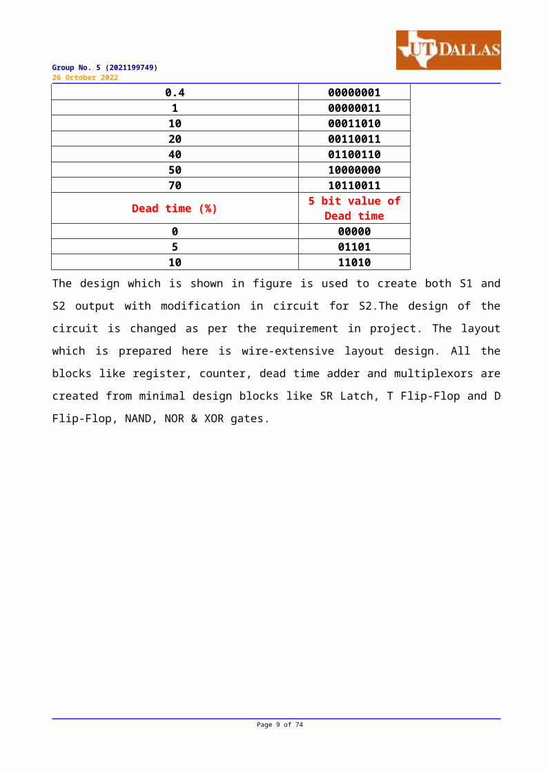
0.4 000000011 0000001110 0001101020 0011001140 0110011050 1000000070 10110011
Dead time (%) 5 bit value ofDead time
0 000005 0110110 11010
The design which is shown in figure is used to create both S1 and
S2 output with modification in circuit for S2.The design of the
circuit is changed as per the requirement in project. The layout
which is prepared here is wire-extensive layout design. All the
blocks like register, counter, dead time adder and multiplexors are
created from minimal design blocks like SR Latch, T Flip-Flop and D
Flip-Flop, NAND, NOR & XOR gates.
Page 9 of 74
Group No. 5 (2021199749)26 October 2022
Chapter 2
Basic Circuit Block Design
Details: In this chapter, all the basic building blocks’ schematic level
diagram, layout diagram and simulation results are shown. All the
schematics are made in cadence tool and simulated in cadence tool.
All the layouts are made in Cadence virtuoso tool and simulated
using HSPICE netlist. In the end of the chapter, the summary of all
devices is given. In it the worst case delay, area (um2), power
dissipation and energy is shown. All the simulations are done form
0ns to 10ns with step of 1ns, so power and energy are as calculated
as per that specification.
All the simulations of all the blocks are done as per instruction
with load of four 1X inverters which are connected with output. All
the images are taken using Snipping tool and Paint tool to invert
color for better resolution.
Page 10 of 74
Group No. 5 (2021199749)26 October 2022
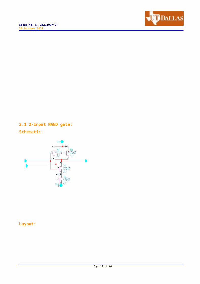
2.1 2-Input NAND gate:Schematic:
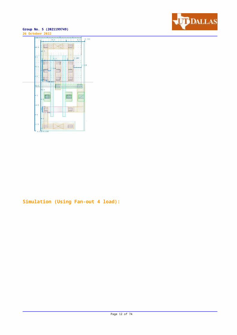
Layout:
Page 11 of 74
Group No. 5 (2021199749)26 October 2022
Simulation (Using Fan-out 4 load):
Page 12 of 74
Group No. 5 (2021199749)26 October 2022
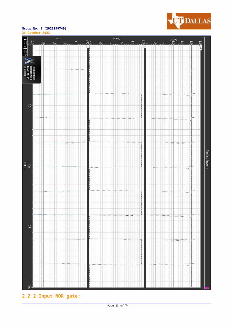
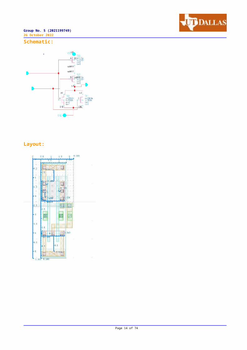
2.2 2 Input NOR gate:Page 13 of 74
Group No. 5 (2021199749)26 October 2022
Schematic:
Layout:
Page 14 of 74
Group No. 5 (2021199749)26 October 2022
Simulation (Using Fan-out 4 load):
Page 15 of 74
Group No. 5 (2021199749)26 October 2022
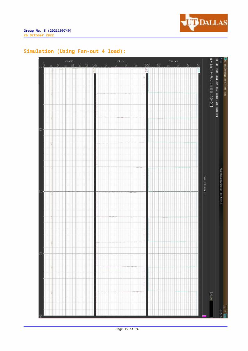
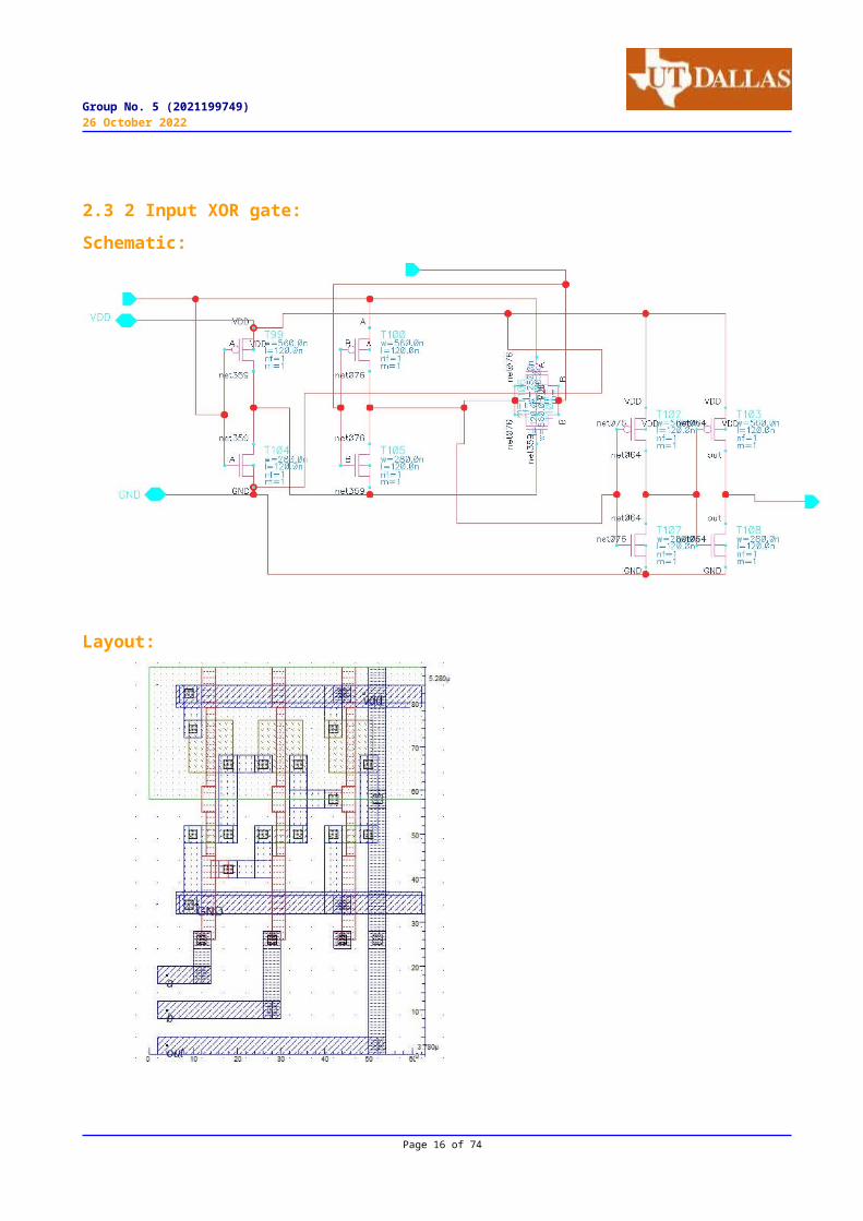
2.3 2 Input XOR gate:Schematic:
Layout:
Page 16 of 74

Group No. 5 (2021199749)26 October 2022
Simulation Result (Using Fan-out 4 load)
Page 17 of 74
Group No. 5 (2021199749)26 October 2022
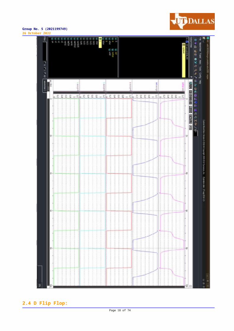
2.4 D Flip Flop:Page 18 of 74
Group No. 5 (2021199749)26 October 2022
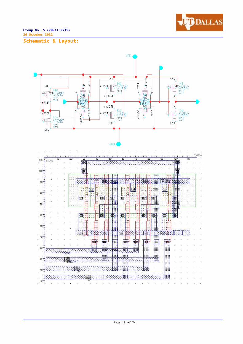
Schematic & Layout:
Page 19 of 74
Group No. 5 (2021199749)26 October 2022
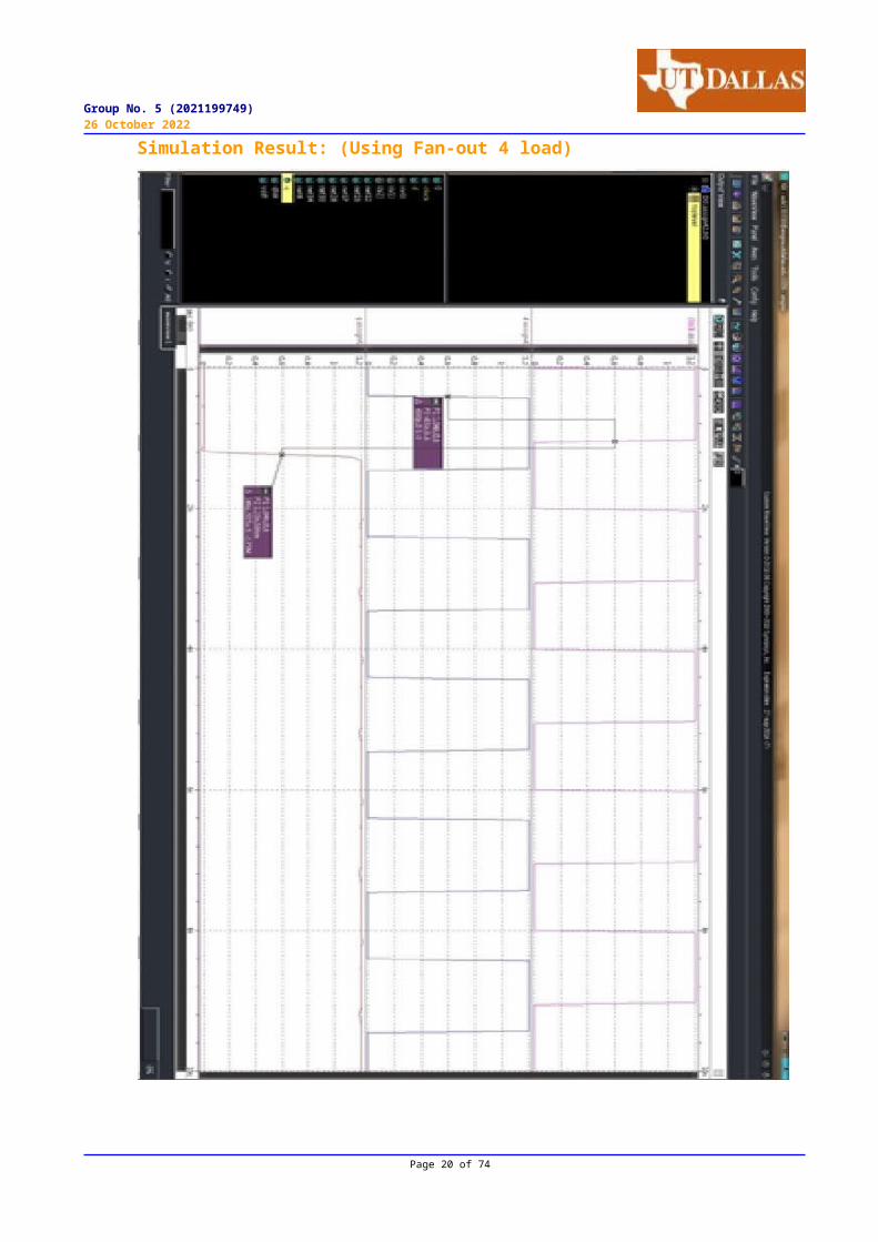
Simulation Result: (Using Fan-out 4 load)
Page 20 of 74
Group No. 5 (2021199749)26 October 2022
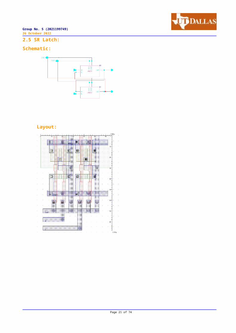
2.5 SR Latch:Schematic:
Layout:
Page 21 of 74
Group No. 5 (2021199749)26 October 2022
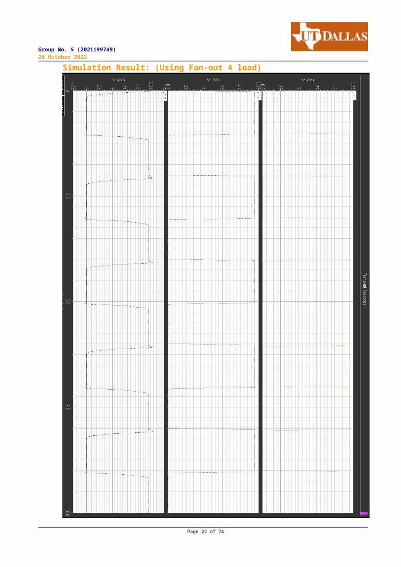
Simulation Result: (Using Fan-out 4 load)
Page 22 of 74
Group No. 5 (2021199749)26 October 2022
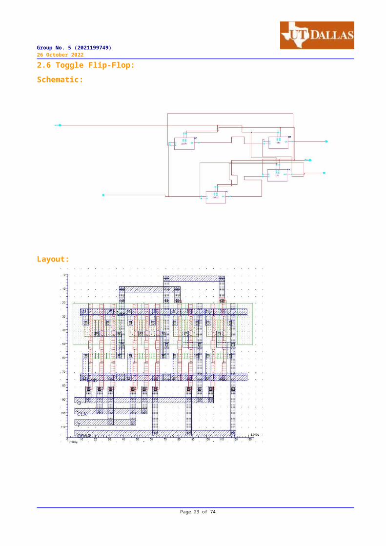
2.6 Toggle Flip-Flop:Schematic:
Layout:
Page 23 of 74

Group No. 5 (2021199749)26 October 2022
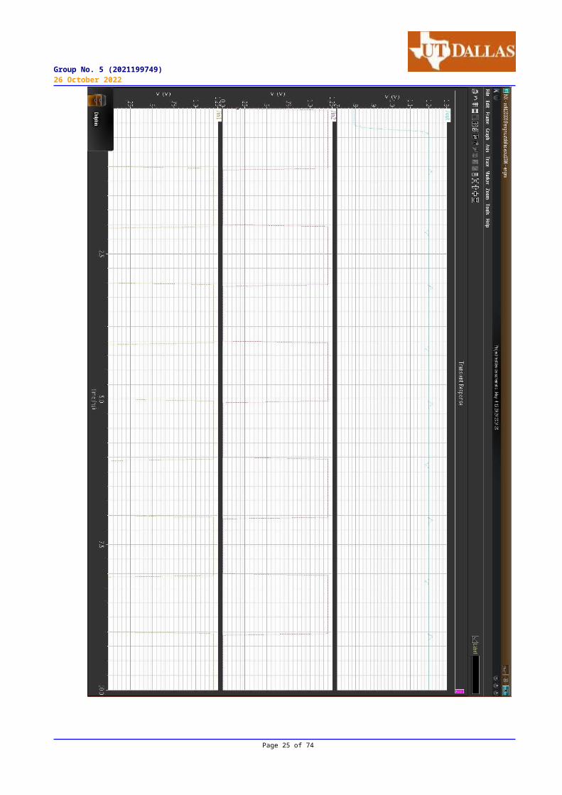
Simulation Result: (Using Fan-out 4 load)
Page 24 of 74
Group No. 5 (2021199749)26 October 2022
Page 25 of 74
Group No. 5 (2021199749)26 October 2022
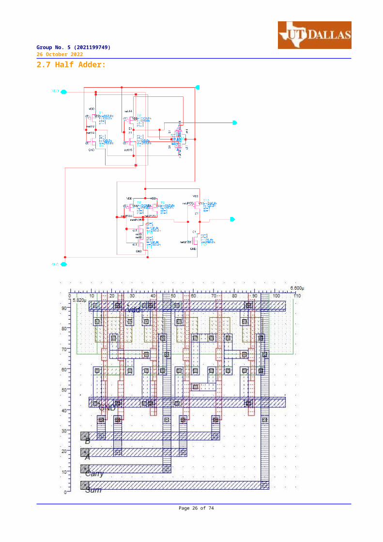
2.7 Half Adder:
Page 26 of 74

Group No. 5 (2021199749)26 October 2022
Simulation Result: (Using Fan-out 4 load)
Page 27 of 74
Group No. 5 (2021199749)26 October 2022
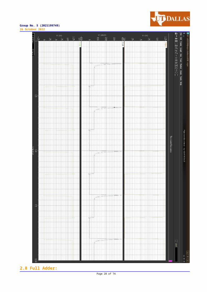
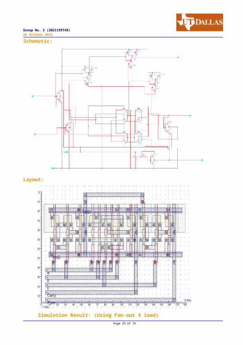
2.8 Full Adder:Page 28 of 74
Group No. 5 (2021199749)26 October 2022
Schematic:
Layout:
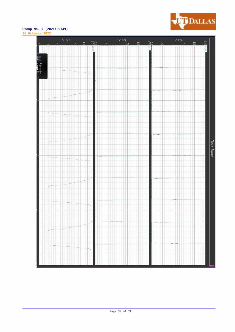
Simulation Result: (Using Fan-out 4 load)Page 29 of 74
Group No. 5 (2021199749)26 October 2022
Page 30 of 74
Group No. 5 (2021199749)26 October 2022
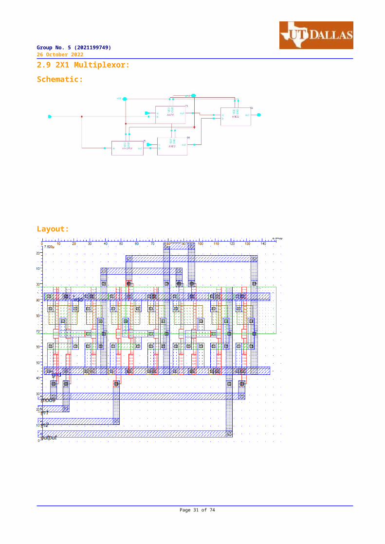
2.9 2X1 Multiplexor:Schematic:
Layout:
Page 31 of 74

Group No. 5 (2021199749)26 October 2022
Simulation Result: (Using Fan-out 4 load)
Page 32 of 74
Group No. 5 (2021199749)26 October 2022
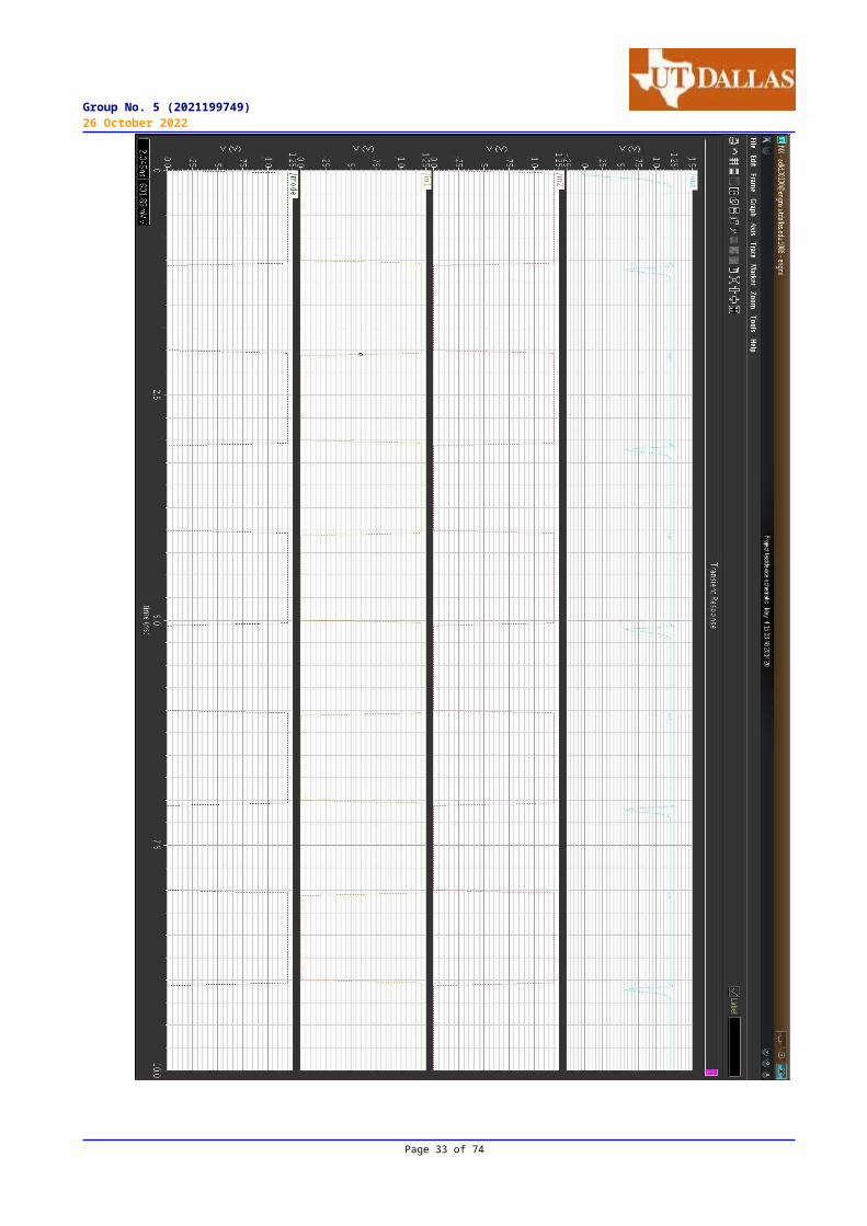
Page 33 of 74
Group No. 5 (2021199749)26 October 2022
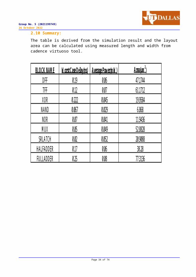
2.10 Summary:The table is derived from the simulation result and the layoutarea can be calculated using measured length and width from cadence virtuoso tool.
BLO CK NAM E W orst Case Delay(ns) Average Power(m W ) Area(um 2)DFF 0.19 0.06 47.1744TFF 0.12 0.07 61.1712XOR 0.222 0.045 19.9584NAND 0.067 0.029 6.868NOR 0.07 0.041 11.9436M UX 0.05 0.049 52.8828
SRLATCH 0.02 0.052 20.9088HALFADDER 0.17 0.06 38.28FULLADDER 0.25 0.08 77.3136
Page 34 of 74
Group No. 5 (2021199749)26 October 2022
Chapter 3
Chip DesignIn chip design, as per proposed block diagram, the counter design
is done and it has to do both up and down counting operation. 8 bit
registers are made to store value for temporary bases such that
until the value comes, old value can be held by device. This
design’s main operation is to provide the power to bigger circuits,
on chip or off chip circuits with programmable interval of period
such that power consumption overall can be reduced while some part
of circuit is not working at that moment. The output is 1.2 V
pulsating output to input of the major circuits so, output of this
design is tested with 4 1X inverters to check its fanout capacity.
In this layout design the tutorial of cadence from Purdue
university is very helpful .
Page 35 of 74
Group No. 5 (2021199749)26 October 2022
3.1 Schematic Design:
Page 36 of 74
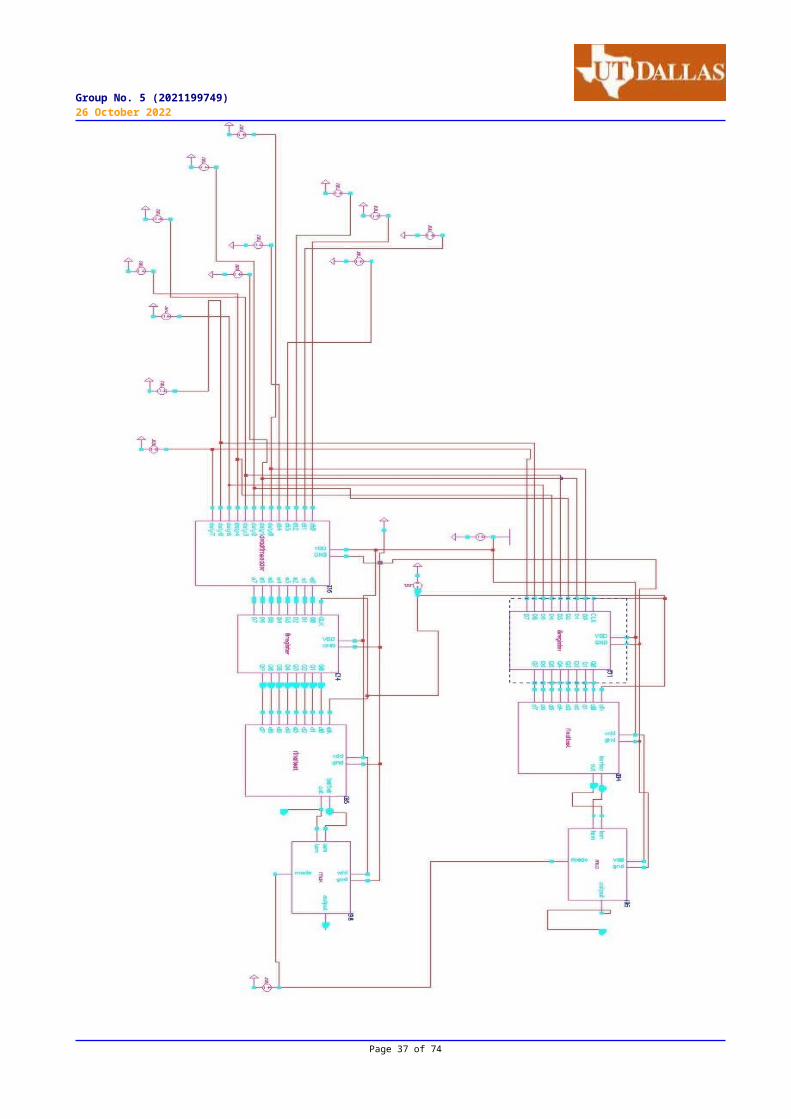
Group No. 5 (2021199749)26 October 2022
Page 37 of 74
Group No. 5 (2021199749)26 October 2022
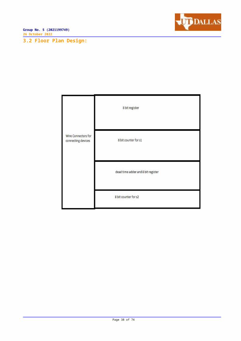
3.2 Floor Plan Design:
Page 38 of 74
Group No. 5 (2021199749)26 October 2022
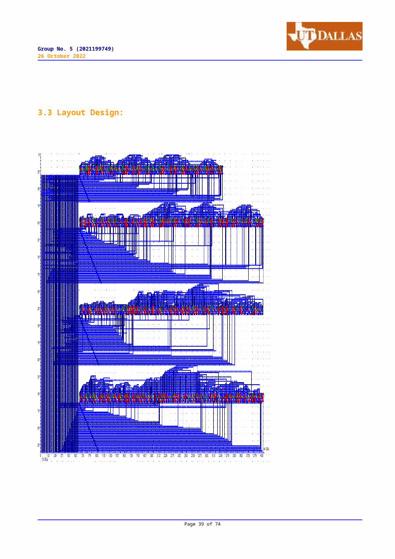
3.3 Layout Design:
Page 39 of 74
Group No. 5 (2021199749)26 October 2022
3.3 Layout Design Summary
Layout: Quantity Description
No. Of Mosfets: 2450 NMOS and PMOS
I/O pins 20 16 input,1VDD,1GND,2Output
VDD wire length 671um length due to wire extensive layout
GND wire length 665um length due to wire extensive layout
As per the floor plan, I have arranged my design .In this design I
have tried to simplify design as much as I can by designing smaller
blocks and connecting them in layout design with connecting and
making bigger blocks and then arranging them in such way that
design area can be minimized and symmetry of design can be
maintained. Parallel I/O lines are used to connecting longer
distance blocks so, I have used them to reduce connection
complexity and faster transfer throughout the line to all block
(i.e CLOCK). Total Area Of the Design is coming out roughly
around=(131.22um X 200.22um) which is arranged in sort of
rectangle.
Page 40 of 74
Group No. 5 (2021199749)26 October 2022
Chapter 4
Complete Functional Simulation
All the simulation are done using HSPICE code or netlist, which is generated by LVS and QRC procedure of layout. This code is simulated using HSPICE simulator in linux and by giving different test vector values the output is generated as below for TEM or LEM mode as per requirement. Switching time or response time calculation and minimum value that can be given to duty input that is also tested in this design simulation. The summary of all simulations is mentioned in the chapter 5 which includes the power dissipation calculation, Energy value and the response time value and resolution also.
Page 41 of 74
Group No. 5 (2021199749)26 October 2022
4.1 TEM MODE OPERATION SIMULATIONS(a) Duty Cycle 40%, Dead Time 10% TEM OUTPUT:
Page 42 of 74
Group No. 5 (2021199749)26 October 2022
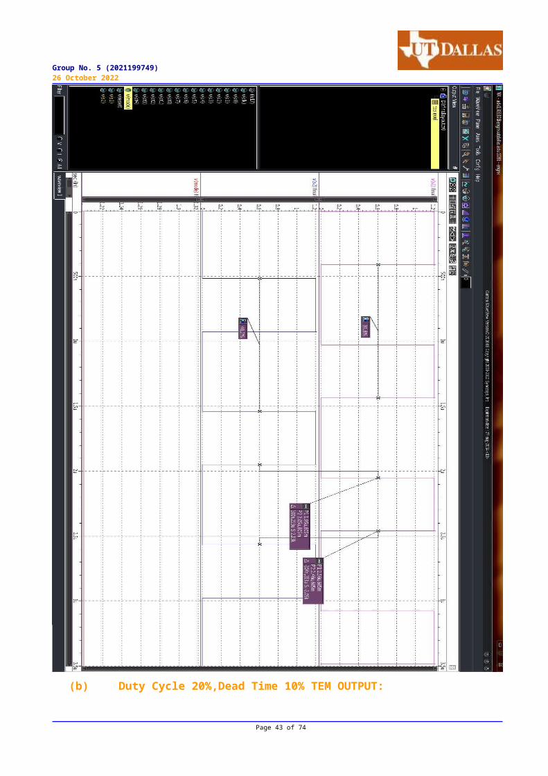
(b) Duty Cycle 20%,Dead Time 10% TEM OUTPUT:
Page 43 of 74
Group No. 5 (2021199749)26 October 2022
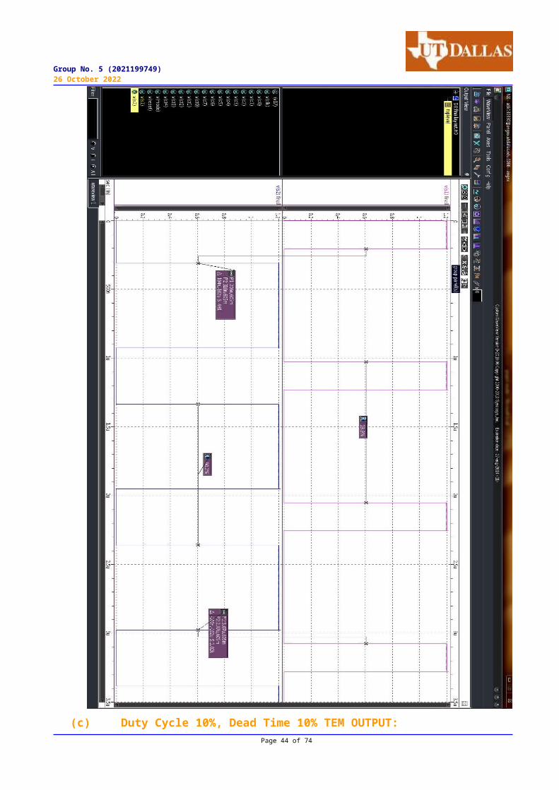
(c) Duty Cycle 10%, Dead Time 10% TEM OUTPUT:Page 44 of 74
Group No. 5 (2021199749)26 October 2022
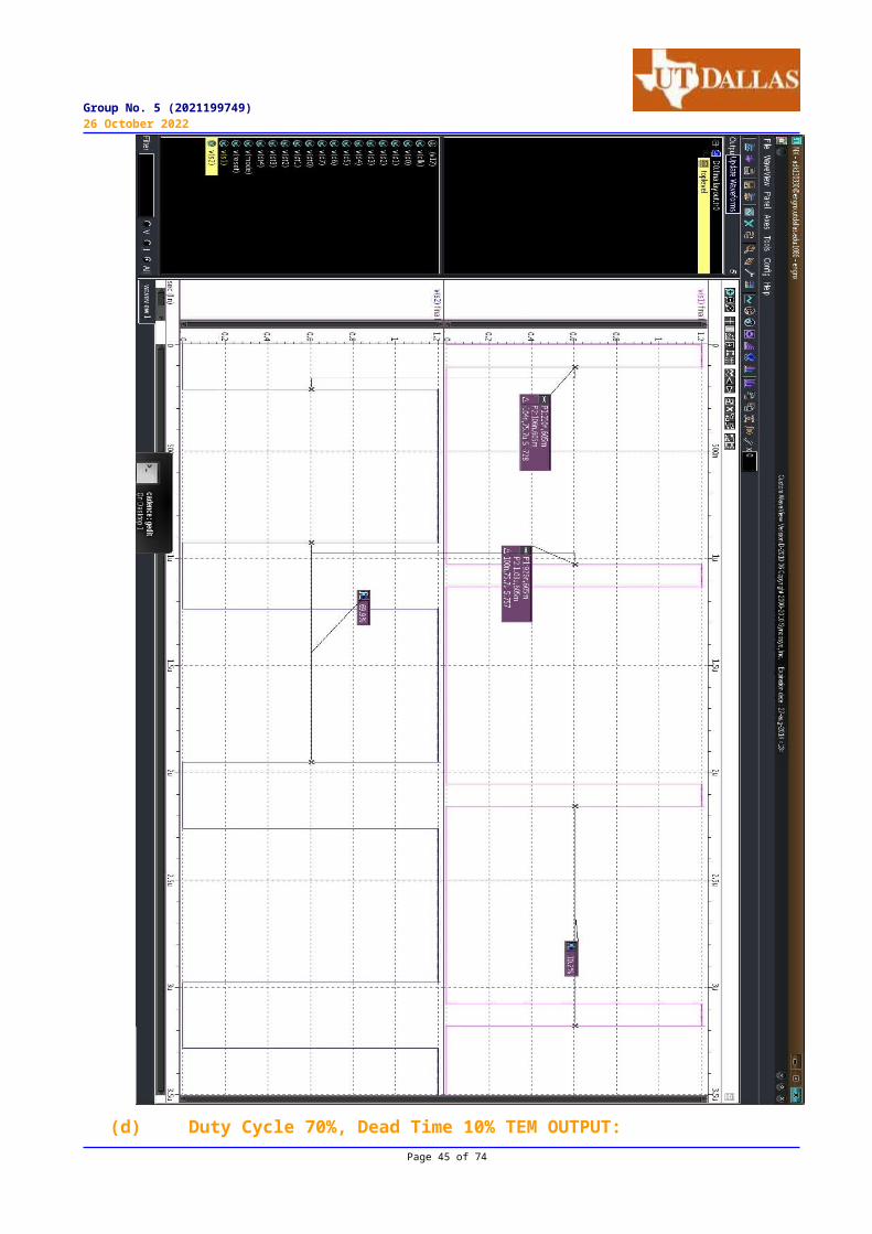
(d) Duty Cycle 70%, Dead Time 10% TEM OUTPUT:Page 45 of 74
Group No. 5 (2021199749)26 October 2022
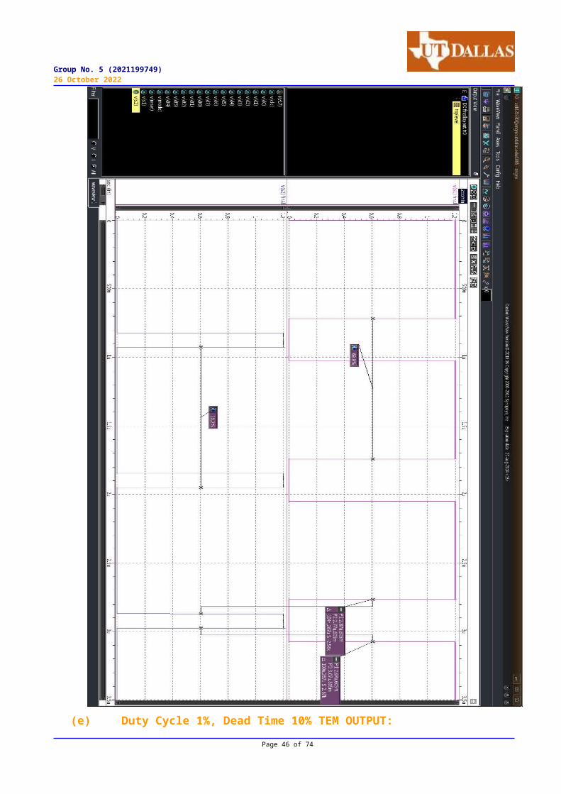
(e) Duty Cycle 1%, Dead Time 10% TEM OUTPUT:Page 46 of 74
Group No. 5 (2021199749)26 October 2022
Page 47 of 74
Group No. 5 (2021199749)26 October 2022
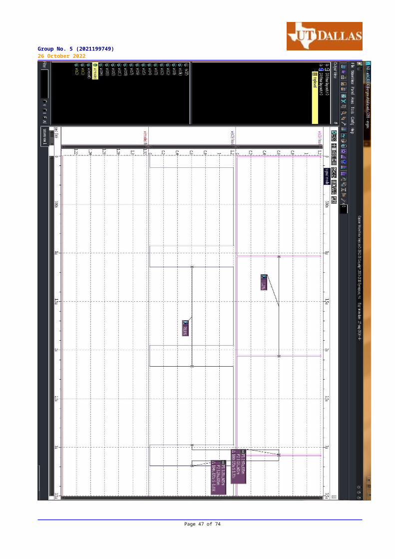
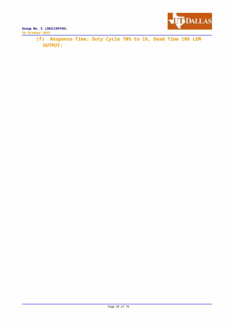
(f) Response Time: Duty Cycle 70% to 1%, Dead Time 10% TEM OUTPUT:
Page 48 of 74
Group No. 5 (2021199749)26 October 2022
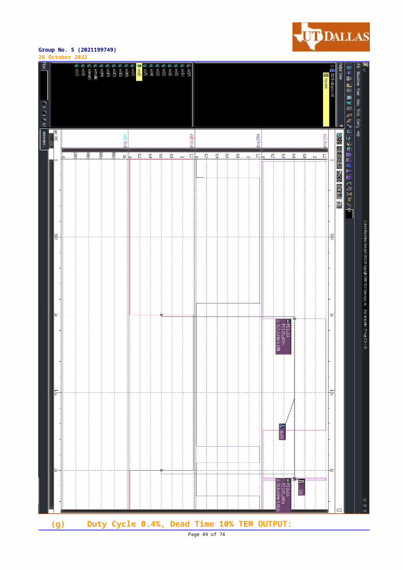
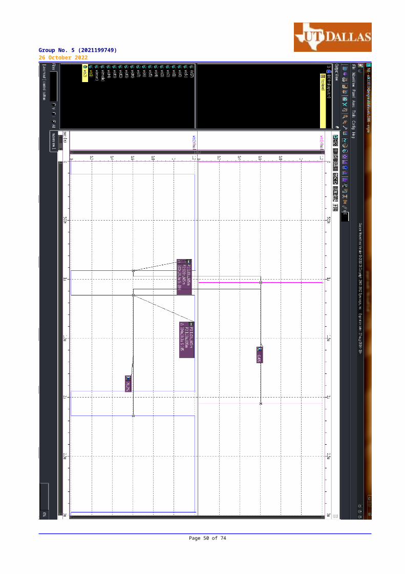
(g) Duty Cycle 0.4%, Dead Time 10% TEM OUTPUT:Page 49 of 74
Group No. 5 (2021199749)26 October 2022
Page 50 of 74
Group No. 5 (2021199749)26 October 2022
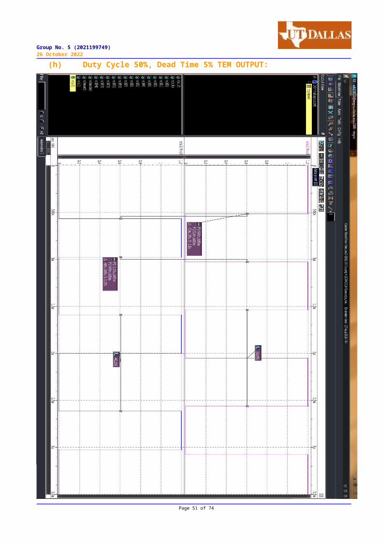
(h) Duty Cycle 50%, Dead Time 5% TEM OUTPUT:
Page 51 of 74
Group No. 5 (2021199749)26 October 2022
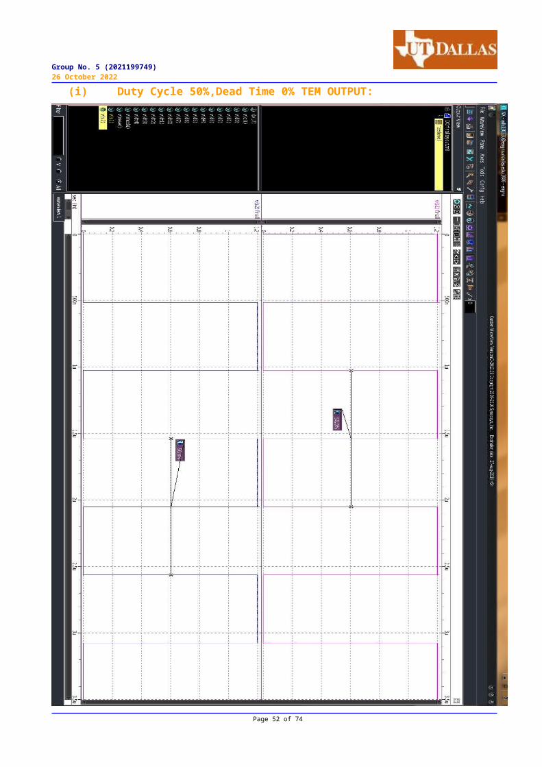
(i) Duty Cycle 50%,Dead Time 0% TEM OUTPUT:
Page 52 of 74
Group No. 5 (2021199749)26 October 2022
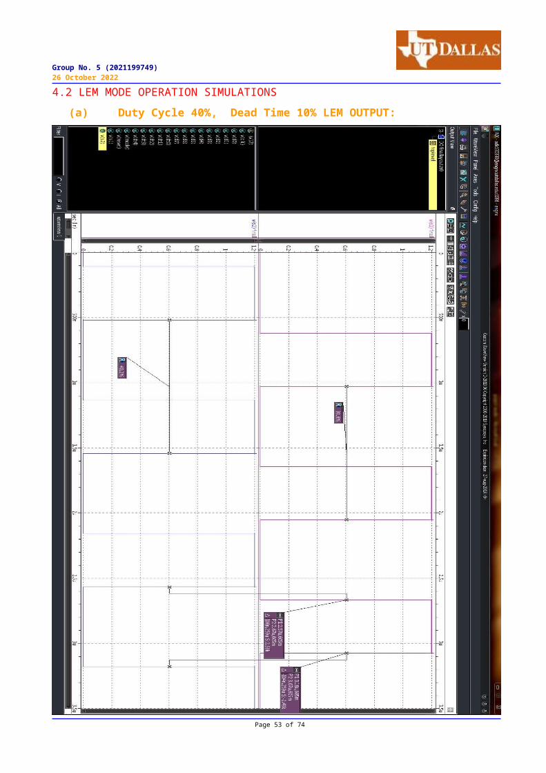
4.2 LEM MODE OPERATION SIMULATIONS(a) Duty Cycle 40%, Dead Time 10% LEM OUTPUT:
Page 53 of 74
Group No. 5 (2021199749)26 October 2022
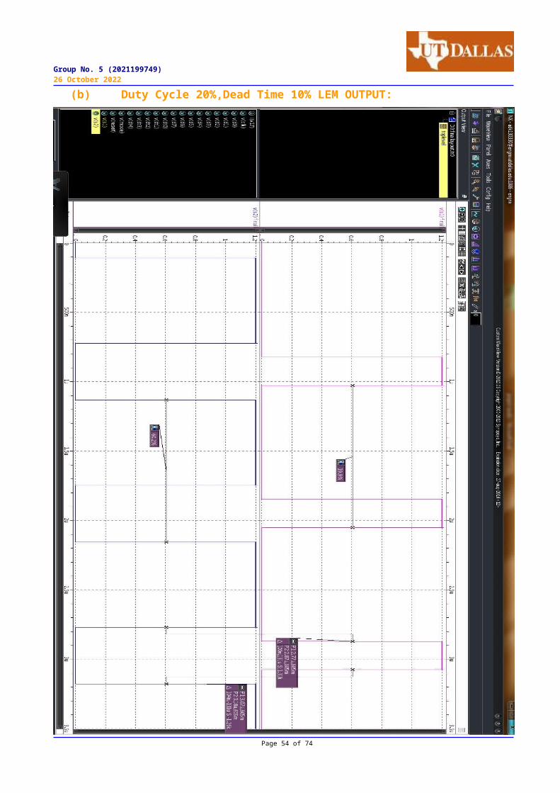
(b) Duty Cycle 20%,Dead Time 10% LEM OUTPUT:
Page 54 of 74
Group No. 5 (2021199749)26 October 2022
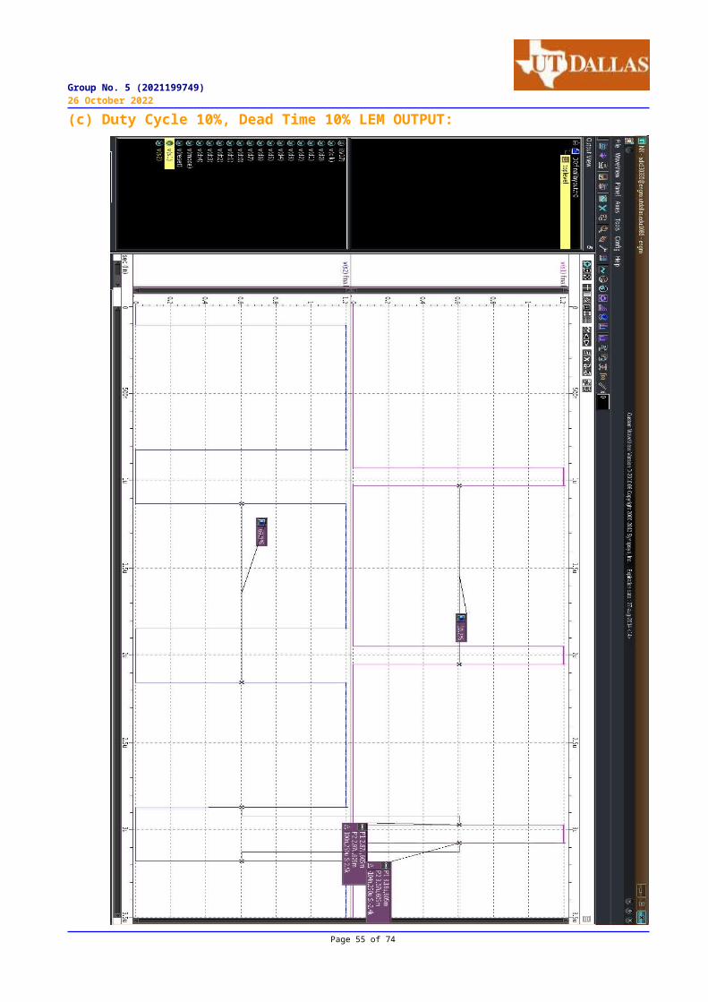
(c) Duty Cycle 10%, Dead Time 10% LEM OUTPUT:
Page 55 of 74

Group No. 5 (2021199749)26 October 2022
(d) Duty Cycle 70%, Dead Time 10% LEM OUTPUT:
Page 56 of 74
Group No. 5 (2021199749)26 October 2022
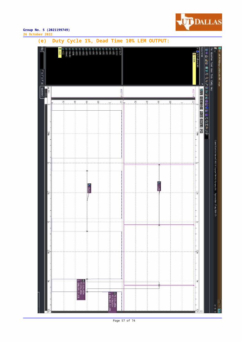
(e) Duty Cycle 1%, Dead Time 10% LEM OUTPUT:
Page 57 of 74
Group No. 5 (2021199749)26 October 2022
(f) Response Time: Duty Cycle 70% to 1%, Dead Time 10% LEM OUTPUT:
Page 58 of 74
Group No. 5 (2021199749)26 October 2022
Page 59 of 74
Group No. 5 (2021199749)26 October 2022
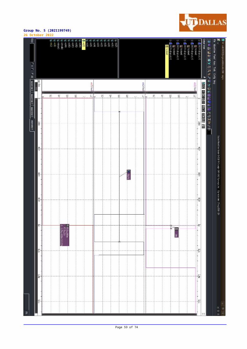
(g) Duty Cycle 0.4%, Dead Time 10% LEM OUTPUT:
Page 60 of 74
Group No. 5 (2021199749)26 October 2022
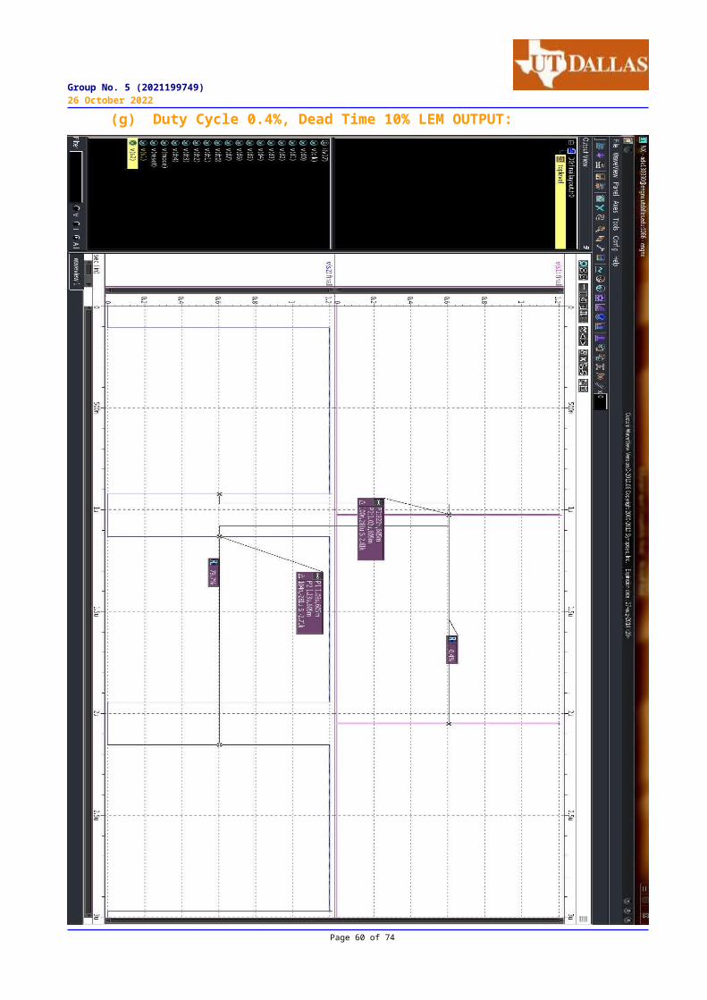
(h) Duty Cycle 50%, Dead Time 5% LEM OUTPUT:
Page 61 of 74
Group No. 5 (2021199749)26 October 2022
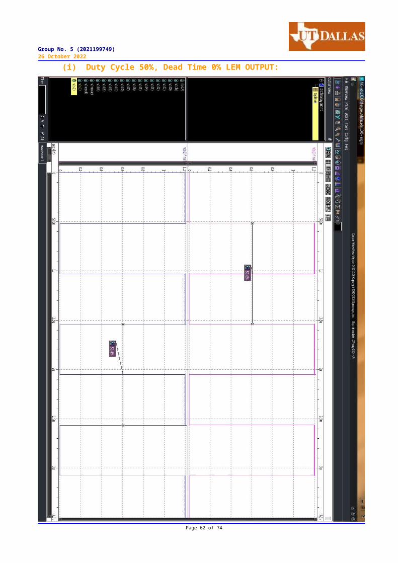
(i) Duty Cycle 50%, Dead Time 0% LEM OUTPUT:
Page 62 of 74
Group No. 5 (2021199749)26 October 2022
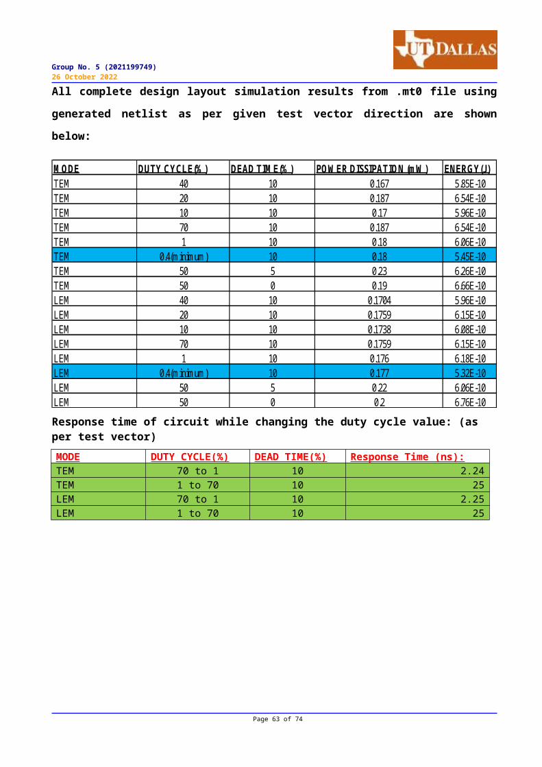
All complete design layout simulation results from .mt0 file using
generated netlist as per given test vector direction are shown
below:
M ODE DUTY CYCLE(% ) DEAD TIM E(% ) POW ER DISSIPATIO N (m W ) ENERGY(J)TEM 40 10 0.167 5.85E-10TEM 20 10 0.187 6.54E-10TEM 10 10 0.17 5.96E-10TEM 70 10 0.187 6.54E-10TEM 1 10 0.18 6.06E-10TEM 0.4(minimum) 10 0.18 5.45E-10TEM 50 5 0.23 6.26E-10TEM 50 0 0.19 6.66E-10LEM 40 10 0.1704 5.96E-10LEM 20 10 0.1759 6.15E-10LEM 10 10 0.1738 6.08E-10LEM 70 10 0.1759 6.15E-10LEM 1 10 0.176 6.18E-10LEM 0.4(minimum) 10 0.177 5.32E-10LEM 50 5 0.22 6.06E-10LEM 50 0 0.2 6.76E-10Response time of circuit while changing the duty cycle value: (as per test vector) MODE DUTY CYCLE(%) DEAD TIME(%) Response Time (ns):TEM 70 to 1 10 2.24TEM 1 to 70 10 25LEM 70 to 1 10 2.25LEM 1 to 70 10 25
Page 63 of 74
Group No. 5 (2021199749)26 October 2022
Chapter 5Conclusion and SummaryThe proposed design was simulated using Cadence tool. The
simulation was performed using the 130nm technology parameters. As
per the project requirement the PWM circuits are used in several
applications, include DC-DC converters wherein they are used to
control one or two switches (S1 and S2) to regulate output voltage
or current. The PWM controller for this project is expected to
produce two outputs, S1 and S2 each capable of producing up to 1
MHz (i.e., Ts=1μs) PWM signal for trailing-edge modulation (TEM) or
leading-edge modulation (LEM).The main challenge is to keep both
switch working but not simultaneously. That will reduce the power.
This all sort of challenges are being fulfilled by design of PWM
controller. The minimum resolution of 0.4% of duty cycle is
attained using 8 bit duty cycle input. Resolution can be made much
more finer but on the cost of power and area and circuit
complexity. Response time is on higher side it can be reduced by
using better connection or design layout techniques like bend
design of mosfets and clock distribution and other better option
which can be considered.
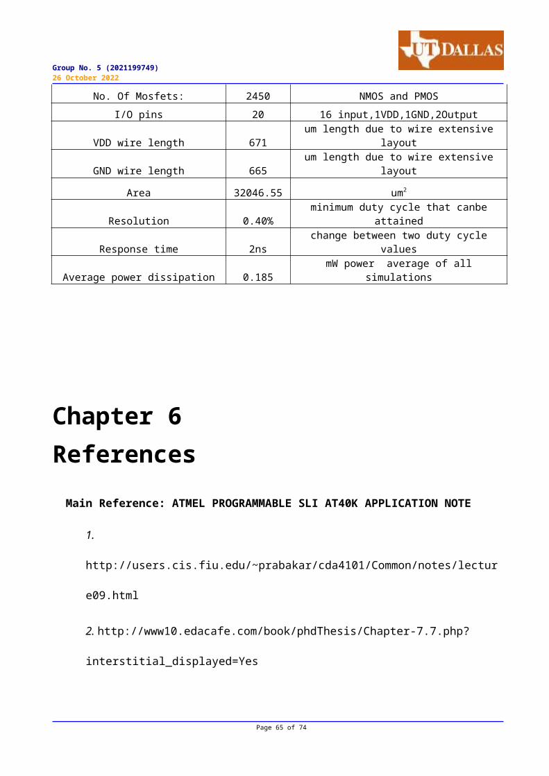
Summary of Design:Layout: Quantity Description
Page 64 of 74
Group No. 5 (2021199749)26 October 2022
No. Of Mosfets: 2450 NMOS and PMOSI/O pins 20 16 input,1VDD,1GND,2Output
VDD wire length 671um length due to wire extensive
layout
GND wire length 665um length due to wire extensive
layout
Area 32046.55 um2
Resolution 0.40%minimum duty cycle that canbe
attained
Response time 2nschange between two duty cycle
values
Average power dissipation 0.185mW power average of all
simulations
Chapter 6References Main Reference: ATMEL PROGRAMMABLE SLI AT40K APPLICATION NOTE
1.
http://users.cis.fiu.edu/~prabakar/cda4101/Common/notes/lectur
e09.html
2. http://www10.edacafe.com/book/phdThesis/Chapter-7.7.php?
interstitial_displayed=Yes
Page 65 of 74
Group No. 5 (2021199749)26 October 2022
3. http://www.edn.com/design/analog/4371393/Understanding-the-
basics-of-setup-and-hold-time
4. http://www.electronics-tutorials.ws/counter/count_4.html
5. http://www.nxp.com/documents/data_sheet/74LVC169.pdf
6.
http://www.doc.ic.ac.uk/~nd/surprise_96/journal/vol4/cwl3/repo
rt.html#xilinx
7. http://www10.edacafe.com/book/phdThesis/Chapter-7.7.php?
interstitial_displayed=Yes
8. http://www.edn.com/design/analog/4371393/Understanding-the-
basics-of-setup-and-hold-time
9. http://www.electronics-tutorials.ws/counter/count_4.html
10. http://www.nxp.com/documents/data_sheet/74LVC169.pdf
11.http://bwrcs.eecs.berkeley.edu/Classes/icdesign/ee141_s04/
CadenceLabs/Lab2/VirtuosoTutorial.htm
12.
https://engineering.purdue.edu/~vlsi/ECE559_Fall09/Lab/559TUT_
3_ver7_fall09.pdf
Page 66 of 74
Group No. 5 (2021199749)26 October 2022
13.
http://inst.eecs.berkeley.edu/~ee105/fa07/tutorials/HSPICE_Tut
orial.pdf
14. http://www.doc.ic.ac.uk/~nd/surprise_96/journal/vol4/cwl3/report.html#xilinx
Appendix:1.Capacitor Card Of Layout:
Page 67 of 74
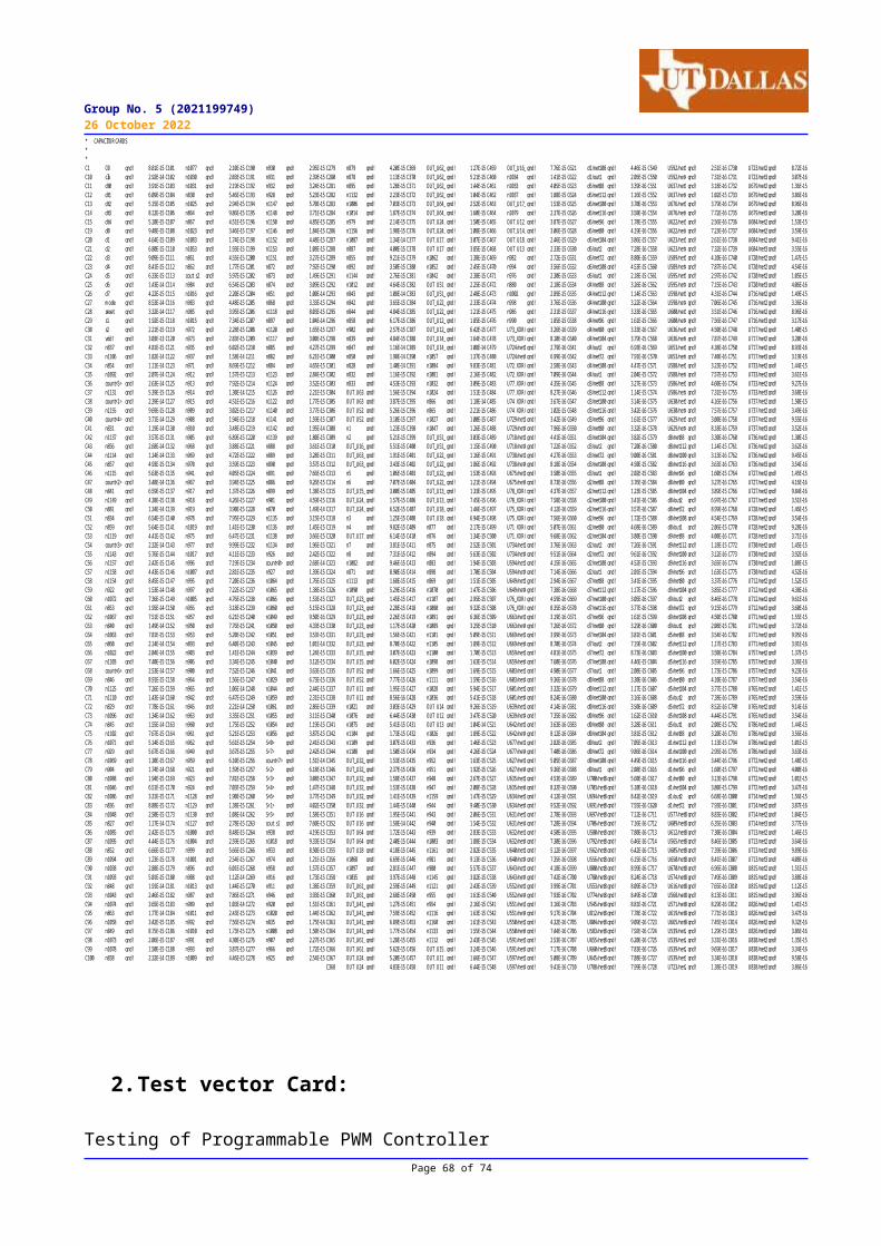
Group No. 5 (2021199749)26 October 2022* CAPACITOR CARDS**C1 C0 gnd! 8.81E-15 C101 n1077 gnd! 2.10E-15 C190 n930 gnd! 2.95E-15 C279 n879 gnd! 4.20E-15 C369 OUT_U62_NORgnd! 1.27E-15 C459 OUT_U16_NOR_2gnd! 7.76E-15 C621 d1/net108 gnd! 4.46E-15 C549 U592/net10gnd! 2.51E-16 C730 U723/net25gnd! 8.72E-16C10 clk gnd! 2.92E-14 C102 n1030 gnd! 2.03E-15 C191 n931 gnd! 2.39E-15 C280 n878 gnd! 1.13E-15 C370 OUT_U62_INV_2gnd! 5.21E-15 C460 n1034 gnd! 1.41E-15 C622 d1/out1 gnd! 2.05E-15 C550 U592/net43gnd! 7.31E-16 C731 U723/net36gnd! 3.07E-16C11 dt0 gnd! 3.91E-15 C103 n1031 gnd! 2.19E-15 C192 n932 gnd! 3.24E-15 C281 n895 gnd! 1.28E-15 C371 OUT_U62_NANDgnd! 1.44E-15 C461 n1033 gnd! 4.05E-15 C623 d6/net88 gnd! 3.39E-16 C551 U637/net10gnd! 3.18E-16 C732 U679/net29gnd! 1.36E-15C12 dt1 gnd! 6.09E-15 C104 n830 gnd! 5.46E-15 C193 n928 gnd! 5.23E-15 C282 n1132 gnd! 2.23E-15 C372 OUT_U62_INV_1gnd! 1.04E-15 C462 n1037 gnd! 1.88E-15 C624 d6/net112 gnd! 1.16E-15 C552 U637/net43gnd! 1.02E-15 C733 U679/net20gnd! 3.86E-16C13 dt2 gnd! 5.15E-15 C105 n1025 gnd! 2.94E-15 C194 n1147 gnd! 5.70E-15 C283 n1006 gnd! 7.03E-15 C373 OUT_U64_NORgnd! 2.52E-15 C463 OUT_U17_NOR_2gnd! 1.53E-15 C625 d6/net100 gnd! 3.70E-16 C553 U676/net10gnd! 3.79E-16 C734 U679/net25gnd! 8.96E-16C14 dt3 gnd! 8.12E-15 C106 n864 gnd! 9.86E-15 C195 n1148 gnd! 3.71E-15 C284 n1014 gnd! 1.87E-15 C374 OUT_U64_INV_2gnd! 1.60E-15 C464 n1079 gnd! 2.37E-15 C626 d6/net116 gnd! 3.50E-16 C554 U676/net43gnd! 7.72E-16 C735 U679/net36gnd! 3.20E-16C15 dt4 gnd! 5.10E-15 C107 n867 gnd! 4.51E-15 C196 n1150 gnd! 4.85E-15 C285 n979 gnd! 2.14E-15 C375 OUT_U24_NAND_2gnd! 1.50E-15 C465 OUT_U12_NOR_2gnd! 3.87E-15 C627 d6/net96 gnd! 1.78E-15 C555 U622/net10gnd! 2.56E-16 C736 U684/net29gnd! 1.53E-15C19 d0 gnd! 9.48E-15 C108 n1023 gnd! 3.46E-15 C197 n1146 gnd! 1.84E-15 C286 n1156 gnd! 1.98E-15 C376 OUT_U24_INV_2gnd! 1.08E-15 C466 OUT_U14_NOR_2gnd! 3.06E-15 C628 d6/net80 gnd! 4.19E-16 C556 U622/net43gnd! 7.23E-16 C737 U684/net20gnd! 3.59E-16C20 d1 gnd! 4.64E-15 C109 n1083 gnd! 1.74E-15 C198 n1152 gnd! 4.48E-15 C287 n1087 gnd! 1.34E-14 C377 OUT_U17_NANDgnd! 3.07E-15 C467 OUT_U18_NOR_2gnd! 2.46E-15 C629 d6/net104 gnd! 3.86E-15 C557 U623/net10gnd! 2.61E-16 C738 U684/net25gnd! 9.41E-16C21 d2 gnd! 6.80E-15 C110 n1053 gnd! 1.93E-15 C199 n1153 gnd! 1.08E-15 C288 n887 gnd! 4.00E-15 C378 OUT_U17_INVgnd! 3.85E-15 C468 OUT_U13_NOR_2gnd! 2.33E-15 C630 d6/out2 gnd! 7.28E-16 C558 U623/net43gnd! 7.32E-16 C739 U684/net36gnd! 3.55E-16C22 d3 gnd! 9.09E-15 C111 n861 gnd! 4.55E-15 C200 n1151 gnd! 3.27E-15 C289 n855 gnd! 9.21E-15 C379 n1062 gnd! 1.38E-15 C469 n982 gnd! 2.72E-15 C631 d6/net72 gnd! 8.80E-16 C559 U589/net10gnd! 4.10E-16 C740 U720/net29gnd! 1.47E-15C23 d4 gnd! 8.41E-15 C112 n862 gnd! 1.77E-15 C201 n872 gnd! 7.92E-15 C290 n892 gnd! 3.50E-15 C380 n1052 gnd! 2.45E-15 C470 n994 gnd! 3.56E-15 C632 d6/net108 gnd! 4.53E-15 C560 U589/net43gnd! 7.87E-16 C741 U720/net20gnd! 4.54E-16C24 d5 gnd! 6.33E-15 C113 cout_s2 gnd! 5.97E-15 C202 n873 gnd! 1.49E-15 C291 n1144 gnd! 2.76E-15 C381 n1042 gnd! 2.38E-15 C471 n976 gnd! 2.30E-15 C633 d6/out1 gnd! 2.18E-15 C561 U595/net10gnd! 2.97E-16 C742 U720/net25gnd! 1.05E-15C25 d6 gnd! 1.43E-14 C114 n984 gnd! 6.54E-15 C203 n874 gnd! 3.09E-15 C292 n1012 gnd! 4.64E-15 C382 OUT_U51_NORgnd! 2.25E-15 C472 n880 gnd! 2.18E-15 C634 d4/net88 gnd! 3.26E-16 C562 U595/net43gnd! 7.15E-16 C743 U720/net36gnd! 4.06E-16C26 d7 gnd! 4.22E-15 C115 n1016 gnd! 2.20E-15 C204 n851 gnd! 1.00E-14 C293 n843 gnd! 1.08E-14 C383 OUT_U51_INV_2gnd! 2.48E-15 C473 n1002 gnd! 2.89E-15 C635 d4/net112 gnd! 1.14E-15 C563 U598/net10gnd! 4.31E-16 C744 U716/net29gnd! 1.49E-15C27 m ode gnd! 8.53E-14 C116 n983 gnd! 4.48E-15 C205 n868 gnd! 3.33E-15 C294 n842 gnd! 3.65E-15 C384 OUT_U22_NAND_1gnd! 2.33E-15 C474 n998 gnd! 3.76E-15 C636 d4/net100 gnd! 3.22E-16 C564 U598/net43gnd! 7.06E-16 C745 U716/net20gnd! 3.36E-16C28 reset gnd! 3.32E-14 C117 n985 gnd! 3.95E-15 C206 n1118 gnd! 8.03E-15 C295 n844 gnd! 4.84E-15 C385 OUT_U22_INV_1gnd! 1.21E-15 C475 n986 gnd! 2.31E-15 C637 d4/net116 gnd! 3.33E-16 C565 U600/net10gnd! 3.51E-16 C746 U716/net25gnd! 8.96E-16C29 s1 gnd! 1.92E-15 C118 n1015 gnd! 7.34E-15 C207 n897 gnd! 1.04E-14 C296 n858 gnd! 6.17E-15 C386 OUT_U12_NANDgnd! 1.85E-15 C476 n990 gnd! 1.85E-15 C638 d4/net96 gnd! 1.61E-15 C566 U600/net43gnd! 7.56E-16 C747 U716/net36gnd! 3.17E-16C30 s2 gnd! 2.21E-15 C119 n972 gnd! 2.28E-15 C208 n1120 gnd! 1.65E-15 C297 n902 gnd! 2.57E-15 C387 OUT_U12_INVgnd! 6.42E-15 C477 U73_XOR/net10gnd! 3.26E-16 C639 d4/net80 gnd! 3.33E-16 C567 U636/net10gnd! 4.50E-16 C748 U717/net29gnd! 1.40E-15C31 vdd! gnd! 3.03E-13 C120 n973 gnd! 2.83E-15 C209 n1117 gnd! 3.00E-15 C298 n839 gnd! 4.84E-15 C388 OUT_U14_NANDgnd! 1.64E-15 C478 U73_XOR/net43gnd! 8.10E-16 C640 d4/net104 gnd! 3.79E-15 C568 U636/net43gnd! 7.87E-16 C749 U717/net20gnd! 3.20E-16C32 n837 gnd! 4.81E-15 C121 n935 gnd! 6.02E-15 C210 n885 gnd! 4.27E-15 C299 n847 gnd! 1.16E-14 C389 OUT_U14_INVgnd! 1.08E-14 C479 U724/net10gnd! 2.79E-16 C641 d4/out2 gnd! 6.93E-16 C569 U653/net10gnd! 4.38E-16 C750 U717/net25gnd! 8.93E-16C33 n1106 gnd! 1.82E-14 C122 n937 gnd! 1.58E-14 C211 n882 gnd! 6.21E-15 C300 n850 gnd! 1.98E-14 C390 n1057 gnd! 1.37E-15 C480 U724/net43gnd! 6.99E-16 C642 d4/net72 gnd! 7.91E-16 C570 U653/net43gnd! 7.40E-16 C751 U717/net36gnd! 3.19E-16C34 n854 gnd! 1.11E-14 C123 n971 gnd! 8.69E-15 C212 n884 gnd! 4.65E-15 C301 n828 gnd! 1.40E-14 C391 n1084 gnd! 9.83E-15 C481 U72_XOR/net10gnd! 2.58E-16 C643 d4/net108 gnd! 4.47E-15 C571 U588/net10gnd! 3.23E-16 C752 U733/net29gnd! 1.44E-15C35 n1092 gnd! 2.07E-14 C124 n912 gnd! 1.57E-15 C213 n1123 gnd! 2.84E-15 C302 n832 gnd! 1.16E-15 C392 n1081 gnd! 2.16E-15 C482 U72_XOR/net43gnd! 7.09E-16 C644 d4/out1 gnd! 2.04E-15 C572 U588/net43gnd! 7.57E-16 C753 U733/net20gnd! 3.61E-16C36 count<5> gnd! 2.63E-14 C125 n913 gnd! 7.92E-15 C214 n1124 gnd! 3.52E-15 C303 n833 gnd! 4.53E-15 C393 n1032 gnd! 3.09E-15 C483 U77_XOR/net10gnd! 4.35E-16 C645 d3/net88 gnd! 3.27E-16 C573 U586/net10gnd! 4.60E-16 C754 U733/net25gnd! 9.27E-16C37 n1131 gnd! 5.39E-15 C126 n914 gnd! 1.30E-14 C215 n1126 gnd! 2.21E-15 C304 OUT_U63_NANDgnd! 1.56E-15 C394 n1024 gnd! 1.51E-15 C484 U77_XOR/net43gnd! 8.27E-16 C646 d3/net112 gnd! 1.14E-15 C574 U586/net43gnd! 7.31E-16 C755 U733/net36gnd! 3.68E-16C38 count<1> gnd! 2.39E-14 C127 n915 gnd! 4.51E-15 C216 n1122 gnd! 1.77E-15 C305 OUT_U63_INV_1gnd! 3.87E-15 C395 n866 gnd! 1.18E-14 C485 U74_XOR/net10gnd! 3.67E-16 C647 d3/net100 gnd! 3.14E-16 C575 U630/net10gnd! 4.16E-16 C756 U737/net29gnd! 1.50E-15C39 n1155 gnd! 9.69E-15 C128 n909 gnd! 3.02E-15 C217 n1140 gnd! 3.77E-15 C306 OUT_U52_NORgnd! 5.26E-15 C396 n865 gnd! 2.21E-15 C486 U74_XOR/net43gnd! 1.02E-15 C648 d3/net116 gnd! 3.42E-16 C576 U630/net43gnd! 7.57E-16 C757 U737/net20gnd! 3.49E-16C40 count<4> gnd! 3.71E-14 C129 n908 gnd! 1.94E-15 C218 n1141 gnd! 1.59E-15 C307 OUT_U52_INV_2gnd! 3.10E-15 C397 n1027 gnd! 1.00E-15 C487 U729/net10gnd! 3.42E-16 C649 d3/net96 gnd! 1.61E-15 C577 U629/net10gnd! 3.00E-16 C758 U737/net25gnd! 9.55E-16C41 n831 gnd! 1.19E-14 C130 n910 gnd! 3.48E-15 C219 n1142 gnd! 1.95E-14 C308 n1 gnd! 1.23E-15 C398 n1047 gnd! 1.26E-15 C488 U729/net43gnd! 7.96E-16 C650 d3/net80 gnd! 3.32E-16 C578 U629/net43gnd! 8.18E-16 C759 U737/net36gnd! 3.52E-16C42 n1137 gnd! 3.57E-15 C131 n905 gnd! 6.89E-15 C220 n1139 gnd! 1.80E-15 C309 n2 gnd! 5.21E-15 C399 OUT_U51_NANDgnd! 3.03E-15 C489 U718/net10gnd! 4.41E-16 C651 d3/net104 gnd! 3.82E-15 C579 d8/net88 gnd! 3.30E-16 C760 U736/net29gnd! 1.30E-15C43 n856 gnd! 2.68E-14 C132 n968 gnd! 3.88E-15 C221 n888 gnd! 3.61E-15 C310 OUT_U16_NOR_1gnd! 5.51E-15 C400 OUT_U51_INV_1gnd! 1.15E-15 C490 U718/net43gnd! 7.22E-16 C652 d3/out2 gnd! 7.20E-16 C580 d8/net112 gnd! 1.14E-15 C761 U736/net20gnd! 3.62E-16C44 n1114 gnd! 1.14E-14 C133 n969 gnd! 4.72E-15 C222 n889 gnd! 3.28E-15 C311 OUT_U63_NORgnd! 1.91E-15 C401 OUT_U22_NORgnd! 1.16E-15 C491 U738/net10gnd! 4.27E-16 C653 d3/net72 gnd! 9.00E-16 C581 d8/net100 gnd! 3.13E-16 C762 U736/net25gnd! 9.45E-16C45 n857 gnd! 4.93E-15 C134 n970 gnd! 3.59E-15 C223 n890 gnd! 3.57E-15 C312 OUT_U63_INV_2gnd! 3.43E-15 C402 OUT_U22_INV_3gnd! 1.86E-15 C492 U738/net43gnd! 8.18E-16 C654 d3/net108 gnd! 4.50E-15 C582 d8/net116 gnd! 3.63E-16 C763 U736/net36gnd! 3.54E-16C46 n1115 gnd! 5.63E-15 C135 n941 gnd! 4.05E-15 C224 n891 gnd! 7.66E-15 C313 n5 gnd! 1.06E-15 C403 OUT_U22_NAND_2gnd! 1.53E-15 C493 U675/net10gnd! 3.50E-16 C655 d3/out1 gnd! 2.02E-15 C583 d8/net96 gnd! 1.60E-15 C764 U727/net29gnd! 1.45E-15C47 count<2> gnd! 3.48E-14 C136 n967 gnd! 3.94E-15 C225 n886 gnd! 9.26E-15 C314 n6 gnd! 7.07E-15 C404 OUT_U22_INV_2gnd! 1.21E-15 C494 U675/net43gnd! 8.73E-16 C656 d2/net88 gnd! 3.76E-16 C584 d8/net80 gnd! 3.27E-16 C765 U727/net20gnd! 4.16E-16C48 n841 gnd! 6.59E-15 C137 n917 gnd! 1.37E-15 C226 n899 gnd! 1.38E-15 C315 OUT_U15_NOR_1gnd! 3.00E-15 C405 OUT_U13_NANDgnd! 1.33E-15 C495 U78_XOR/net10gnd! 4.37E-16 C657 d2/net112 gnd! 1.23E-15 C585 d8/net104 gnd! 3.89E-15 C766 U727/net25gnd! 9.84E-16C49 n1149 gnd! 4.38E-15 C138 n918 gnd! 4.26E-15 C227 n901 gnd! 4.59E-15 C316 OUT_U24_NAND_1gnd! 1.57E-15 C406 OUT_U13_INVgnd! 7.45E-15 C496 U78_XOR/net43gnd! 7.58E-16 C658 d2/net100 gnd! 3.41E-16 C586 d8/out2 gnd! 6.97E-16 C767 U727/net36gnd! 3.51E-16C50 n881 gnd! 1.34E-14 C139 n919 gnd! 3.90E-15 C228 n870 gnd! 1.49E-14 C317 OUT_U24_INV_1gnd! 6.52E-15 C407 OUT_U18_NANDgnd! 1.46E-15 C497 U75_XOR/net10gnd! 4.12E-16 C659 d2/net116 gnd! 3.57E-16 C587 d8/net72 gnd! 8.99E-16 C768 U728/net29gnd! 1.46E-15C51 n834 gnd! 6.54E-15 C140 n978 gnd! 7.95E-15 C229 n1135 gnd! 3.15E-15 C318 n3 gnd! 1.25E-15 C408 OUT_U18_INVgnd! 6.94E-15 C498 U75_XOR/net43gnd! 7.56E-16 C660 d2/net96 gnd! 1.72E-15 C588 d8/net108 gnd! 4.54E-15 C769 U728/net20gnd! 3.54E-16C52 n859 gnd! 5.64E-15 C141 n1019 gnd! 1.41E-15 C230 n1136 gnd! 1.45E-15 C319 n4 gnd! 9.82E-15 C409 n877 gnd! 2.17E-15 C499 U71_XOR/net10gnd! 5.07E-16 C661 d2/net80 gnd! 4.68E-16 C589 d8/out1 gnd! 2.06E-15 C770 U728/net25gnd! 9.28E-16C53 n1119 gnd! 4.41E-15 C142 n975 gnd! 6.47E-15 C231 n1138 gnd! 3.66E-15 C320 OUT_U17_NOR_1gnd! 6.14E-15 C410 n876 gnd! 1.34E-15 C500 U71_XOR/net43gnd! 9.68E-16 C662 d2/net104 gnd! 3.80E-15 C590 d9/net88 gnd! 4.00E-16 C771 U728/net36gnd! 3.71E-16C54 count<3> gnd! 2.32E-14 C143 n977 gnd! 9.99E-15 C232 n1134 gnd! 1.96E-15 C321 n7 gnd! 3.81E-15 C411 n875 gnd! 2.52E-15 C501 U734/net10gnd! 3.76E-16 C663 d2/out2 gnd! 7.26E-16 C591 d9/net112 gnd! 1.18E-15 C772 U730/net29gnd! 1.45E-15C55 n1143 gnd! 5.76E-15 C144 n1017 gnd! 4.11E-15 C233 n926 gnd! 2.42E-15 C322 n8 gnd! 7.31E-15 C412 n894 gnd! 5.63E-15 C502 U734/net43gnd! 9.51E-16 C664 d2/net72 gnd! 9.61E-16 C592 d9/net100 gnd! 3.12E-16 C773 U730/net20gnd! 3.92E-16C56 n1157 gnd! 2.42E-15 C145 n996 gnd! 7.19E-15 C234 count<0> gnd! 2.68E-14 C323 n1082 gnd! 9.46E-15 C413 n883 gnd! 1.94E-15 C503 U594/net10gnd! 4.15E-16 C665 d2/net108 gnd! 4.52E-15 C593 d9/net116 gnd! 3.65E-16 C774 U730/net25gnd! 1.08E-15C57 n1158 gnd! 4.43E-15 C146 n1007 gnd! 2.81E-15 C235 n927 gnd! 1.39E-15 C324 n871 gnd! 8.90E-15 C414 n898 gnd! 1.70E-15 C504 U594/net43gnd! 7.14E-16 C666 d2/out1 gnd! 2.01E-15 C594 d9/net96 gnd! 1.63E-15 C775 U730/net36gnd! 4.52E-16C58 n1154 gnd! 8.45E-15 C147 n995 gnd! 7.20E-15 C236 n1064 gnd! 1.76E-15 C325 n1113 gnd! 1.68E-15 C415 n869 gnd! 1.51E-15 C505 U649/net10gnd! 2.94E-16 C667 d7/net88 gnd! 3.41E-16 C595 d9/net80 gnd! 3.37E-16 C776 U712/net29gnd! 1.52E-15C59 n922 gnd! 1.53E-14 C148 n997 gnd! 7.22E-15 C237 n1065 gnd! 1.38E-15 C326 n1090 gnd! 5.29E-15 C416 n1070 gnd! 1.47E-15 C506 U649/net43gnd! 7.38E-16 C668 d7/net112 gnd! 1.17E-15 C596 d9/net104 gnd! 3.85E-15 C777 U712/net20gnd! 4.38E-16C60 n1072 gnd! 7.36E-15 C149 n1005 gnd! 4.76E-15 C238 n1066 gnd! 1.53E-15 C327 OUT_U23_NORgnd! 1.45E-15 C417 n1107 gnd! 2.95E-15 C507 U76_XOR/net10gnd! 4.59E-16 C669 d7/net100 gnd! 3.05E-16 C597 d9/out2 gnd! 8.46E-16 C778 U712/net25gnd! 9.61E-16C61 n853 gnd! 1.95E-14 C150 n956 gnd! 3.18E-15 C239 n1060 gnd! 5.15E-15 C328 OUT_U23_INV_3gnd! 2.28E-15 C418 n1080 gnd! 9.32E-15 C508 U76_XOR/net43gnd! 8.35E-16 C670 d7/net116 gnd! 3.77E-16 C598 d9/net72 gnd! 9.15E-16 C779 U712/net36gnd! 3.60E-16C62 n1067 gnd! 7.51E-15 C151 n957 gnd! 6.21E-15 C240 n1049 gnd! 9.50E-16 C329 OUT_U23_NAND_2gnd! 2.26E-15 C419 n1091 gnd! 6.36E-15 C509 U663/net10gnd! 3.19E-16 C671 d7/net96 gnd! 1.61E-15 C599 d9/net108 gnd! 4.50E-15 C780 U771/net29gnd! 1.55E-15C63 n840 gnd! 1.49E-14 C152 n950 gnd! 7.76E-15 C241 n1050 gnd! 4.33E-15 C330 OUT_U23_INV_2gnd! 1.17E-15 C420 n1089 gnd! 3.25E-15 C510 U663/net43gnd! 7.26E-16 C672 d7/net80 gnd! 3.29E-16 C600 d9/out1 gnd! 2.08E-15 C781 U771/net20gnd! 3.72E-16C64 n1063 gnd! 7.81E-15 C153 n953 gnd! 5.20E-15 C242 n1051 gnd! 3.53E-15 C331 OUT_U23_NAND_1gnd! 1.56E-15 C421 n1101 gnd! 5.09E-15 C511 U669/net10gnd! 3.99E-16 C673 d7/net104 gnd! 3.81E-15 C601 d5/net88 gnd! 3.54E-16 C782 U771/net25gnd! 9.95E-16C65 n860 gnd! 2.14E-14 C154 n893 gnd! 6.40E-15 C243 n1045 gnd! 1.01E-14 C332 OUT_U23_INV_1gnd! 8.70E-15 C422 n1105 gnd! 1.89E-15 C512 U669/net43gnd! 8.70E-16 C674 d7/out2 gnd! 7.19E-16 C602 d5/net112 gnd! 1.17E-15 C783 U771/net36gnd! 3.91E-16C66 n1022 gnd! 2.04E-14 C155 n903 gnd! 1.41E-15 C244 n1039 gnd! 1.24E-15 C333 OUT_U15_NANDgnd! 3.07E-15 C423 n1100 gnd! 1.70E-15 C513 U659/net10gnd! 4.81E-16 C675 d7/net72 gnd! 8.73E-16 C603 d5/net100 gnd! 3.50E-16 C784 U757/net29gnd! 1.37E-15C67 n1103 gnd! 7.40E-15 C156 n906 gnd! 3.34E-15 C245 n1040 gnd! 3.12E-15 C334 OUT_U15_INVgnd! 6.02E-15 C424 n1098 gnd! 1.63E-15 C514 U659/net43gnd! 7.60E-16 C676 d7/net108 gnd! 4.46E-15 C604 d5/net116 gnd! 3.59E-16 C785 U757/net20gnd! 3.36E-16C68 count<6> gnd! 2.53E-14 C157 n900 gnd! 7.52E-15 C246 n1041 gnd! 3.63E-15 C335 OUT_U52_NANDgnd! 1.66E-15 C425 n1099 gnd! 1.69E-15 C515 U603/net10gnd! 4.90E-16 C677 d7/out1 gnd! 2.08E-15 C605 d5/net96 gnd! 1.73E-15 C786 U757/net25gnd! 9.23E-16C69 n846 gnd! 8.91E-15 C158 n964 gnd! 1.56E-15 C247 n1029 gnd! 6.73E-15 C336 OUT_U52_INV_1gnd! 7.77E-15 C426 n1111 gnd! 1.59E-15 C516 U603/net43gnd! 9.36E-16 C678 d0/net88 gnd! 3.30E-16 C606 d5/net80 gnd! 4.10E-16 C787 U757/net36gnd! 3.54E-16C70 n1125 gnd! 7.26E-15 C159 n965 gnd! 1.06E-14 C248 n1044 gnd! 2.44E-15 C337 OUT_U11_NANDgnd! 1.95E-15 C427 n1028 gnd! 5.94E-15 C517 U601/net10gnd! 3.32E-16 C679 d0/net112 gnd! 1.17E-15 C607 d5/net104 gnd! 3.77E-15 C788 U765/net29gnd! 1.41E-15C71 n1110 gnd! 1.43E-14 C160 n942 gnd! 6.47E-15 C249 n1059 gnd! 2.31E-15 C338 OUT_U11_INVgnd! 8.56E-16 C428 n1036 gnd! 5.41E-15 C518 U601/net43gnd! 8.24E-16 C680 d0/net100 gnd! 3.16E-16 C608 d5/out2 gnd! 7.38E-16 C789 U765/net20gnd! 3.59E-16C72 n829 gnd! 7.78E-15 C161 n945 gnd! 2.21E-14 C250 n1061 gnd! 2.86E-15 C339 n1021 gnd! 3.03E-15 C429 OUT_U14_NOR_1gnd! 9.26E-15 C519 U639/net10gnd! 4.14E-16 C681 d0/net116 gnd! 3.50E-16 C609 d5/net72 gnd! 8.52E-16 C790 U765/net25gnd! 9.14E-16C73 n1096 gnd! 1.34E-14 C162 n963 gnd! 3.35E-15 C251 n1055 gnd! 3.11E-15 C340 n1076 gnd! 6.44E-15 C430 OUT_U12_NOR_1gnd! 3.47E-15 C520 U639/net43gnd! 7.35E-16 C682 d0/net96 gnd! 1.62E-15 C610 d5/net108 gnd! 4.44E-15 C791 U765/net36gnd! 3.54E-16C74 n845 gnd! 1.55E-14 C163 n960 gnd! 1.75E-15 C252 n1054 gnd! 1.19E-15 C341 n1075 gnd! 5.41E-15 C431 OUT_U13_NOR_1gnd! 1.04E-14 C521 U642/net10gnd! 3.63E-16 C683 d0/net80 gnd! 3.28E-16 C611 d5/out1 gnd! 2.00E-15 C792 U786/net29gnd! 1.44E-15C75 n1102 gnd! 7.67E-15 C164 n961 gnd! 5.21E-15 C253 n1056 gnd! 3.87E-15 C342 n1104 gnd! 1.73E-15 C432 n1026 gnd! 1.89E-15 C522 U642/net43gnd! 8.12E-16 C684 d0/net104 gnd! 3.81E-15 C612 d1/net88 gnd! 3.20E-16 C793 U786/net20gnd! 3.56E-16C76 n1071 gnd! 5.14E-15 C165 n962 gnd! 5.61E-15 C254 S<0> gnd! 2.41E-15 C343 n1109 gnd! 3.07E-15 C433 n936 gnd! 1.46E-15 C523 U677/net10gnd! 2.82E-16 C685 d0/out2 gnd! 7.05E-16 C613 d1/net112 gnd! 1.13E-15 C794 U786/net25gnd! 1.01E-15C77 n929 gnd! 5.67E-15 C166 n949 gnd! 3.67E-15 C255 S<7> gnd! 2.42E-15 C344 n1108 gnd! 1.50E-15 C434 n934 gnd! 4.26E-15 C524 U677/net43gnd! 7.40E-16 C686 d0/net72 gnd! 9.86E-16 C614 d1/net100 gnd! 2.95E-16 C795 U786/net36gnd! 3.63E-16C78 n1069 gnd! 1.30E-15 C167 n959 gnd! 6.10E-15 C256 count<7> gnd! 1.51E-14 C345 OUT_U32_NORgnd! 1.53E-15 C435 n952 gnd! 1.63E-15 C525 U627/net10gnd! 5.05E-16 C687 d0/net108 gnd! 4.49E-15 C615 d1/net116 gnd! 3.44E-16 C796 U772/net29gnd! 1.48E-15C79 n904 gnd! 1.74E-14 C168 n921 gnd! 1.59E-15 C257 S<2> gnd! 6.18E-15 C346 OUT_U32_INV_3gnd! 2.37E-15 C436 n951 gnd! 1.92E-15 C526 U627/net43gnd! 9.36E-16 C688 d0/out1 gnd! 2.08E-15 C616 d1/net96 gnd! 1.60E-15 C797 U772/net20gnd! 4.00E-16C80 n1088 gnd! 1.94E-15 C169 n923 gnd! 7.81E-15 C258 S<3> gnd! 3.08E-15 C347 OUT_U32_NAND_2gnd! 1.58E-15 C437 n948 gnd! 2.67E-15 C527 U635/net10gnd! 4.53E-16 C689 U700/net8gnd! 5.60E-16 C617 d1/net80 gnd! 3.13E-16 C798 U772/net25gnd! 1.01E-15C81 n1046 gnd! 6.51E-15 C170 n924 gnd! 7.03E-15 C259 S<4> gnd! 1.47E-15 C348 OUT_U32_INV_2gnd! 1.53E-15 C438 n947 gnd! 2.08E-15 C528 U635/net43gnd! 8.32E-16 C690 U703/net8gnd! 5.10E-16 C618 d1/net104 gnd! 3.80E-15 C799 U772/net36gnd! 3.47E-16C82 n1086 gnd! 3.31E-15 C171 n1128 gnd! 1.90E-15 C260 S<6> gnd! 3.77E-15 C349 OUT_U32_NAND_1gnd! 1.41E-15 C439 n1159 gnd! 1.47E-15 C529 U634/net10gnd! 4.12E-16 C691 U694/net8gnd! 8.42E-16 C619 d1/out2 gnd! 6.68E-16 C800 U714/net29gnd! 1.56E-15C83 n836 gnd! 8.88E-15 C172 n1129 gnd! 1.38E-15 C261 S<1> gnd! 4.02E-15 C350 OUT_U32_INV_1gnd! 1.44E-15 C440 n944 gnd! 9.40E-15 C530 U634/net43gnd! 9.52E-16 C692 U691/net8gnd! 7.55E-16 C620 d1/net72 gnd! 7.93E-16 C801 U714/net20gnd! 3.87E-16C84 n1048 gnd! 2.50E-15 C173 n1130 gnd! 1.08E-14 C262 S<5> gnd! 1.58E-15 C351 OUT_U16_NANDgnd! 1.95E-15 C441 n943 gnd! 2.06E-15 C531 U631/net10gnd! 2.78E-16 C693 U697/net8gnd! 7.12E-16 C711 U577/net8gnd! 8.83E-16 C802 U714/net25gnd! 1.04E-15C85 n827 gnd! 1.17E-14 C174 n1127 gnd! 2.78E-15 C263 cout_s1 gnd! 7.60E-15 C352 OUT_U16_INVgnd! 1.58E-14 C442 n940 gnd! 1.54E-15 C532 U631/net43gnd! 7.28E-16 C694 U706/net8gnd! 7.16E-16 C712 U609/net8gnd! 6.35E-16 C803 U714/net36gnd! 3.77E-16C86 n1085 gnd! 2.42E-15 C175 n1000 gnd! 8.48E-15 C264 n938 gnd! 4.19E-15 C353 OUT_U64_NANDgnd! 1.72E-15 C443 n939 gnd! 2.83E-15 C533 U632/net10gnd! 4.50E-16 C695 U580/net8gnd! 7.80E-16 C713 U612/net8gnd! 7.30E-16 C804 U713/net29gnd! 1.46E-15C87 n1095 gnd! 4.44E-15 C176 n1004 gnd! 2.59E-15 C265 n1018 gnd! 9.33E-15 C354 OUT_U64_INV_1gnd! 2.40E-15 C444 n1003 gnd! 1.88E-15 C534 U632/net43gnd! 7.30E-16 C696 U792/net8gnd! 6.46E-16 C714 U565/net8gnd! 8.46E-16 C805 U713/net20gnd! 3.64E-16C88 n852 gnd! 6.66E-15 C177 n999 gnd! 5.66E-15 C266 n933 gnd! 8.50E-15 C355 OUT_U18_NOR_1gnd! 4.18E-15 C445 n1161 gnd! 2.82E-15 C535 U640/net10gnd! 5.12E-16 C697 U562/net8gnd! 6.42E-16 C715 U605/net8gnd! 7.39E-16 C806 U713/net25gnd! 9.89E-16C89 n1094 gnd! 1.23E-15 C178 n1001 gnd! 2.54E-15 C267 n974 gnd! 1.21E-15 C356 n1068 gnd! 6.69E-15 C446 n981 gnd! 9.13E-15 C536 U640/net43gnd! 7.35E-16 C698 U556/net8gnd! 6.15E-16 C716 U650/net8gnd! 8.41E-16 C807 U713/net36gnd! 4.08E-16C90 n1038 gnd! 2.88E-15 C179 n896 gnd! 6.01E-15 C268 n958 gnd! 1.57E-15 C357 n1097 gnd! 2.81E-15 C447 n980 gnd! 5.57E-15 C537 U643/net10gnd! 4.18E-16 C699 U800/net8gnd! 8.99E-16 C717 U670/net8gnd! 6.96E-16 C808 U815/net29gnd! 1.51E-15C91 n1093 gnd! 5.01E-15 C180 n988 gnd! 1.12E-14 C269 n916 gnd! 1.73E-15 C358 n1035 gnd! 3.97E-15 C448 n1145 gnd! 3.82E-15 C538 U643/net43gnd! 7.42E-16 C700 U780/net8gnd! 8.24E-16 C718 U574/net8gnd! 7.49E-16 C809 U815/net20gnd! 3.88E-16C92 n848 gnd! 1.91E-14 C181 n1013 gnd! 1.44E-15 C270 n911 gnd! 1.38E-15 C359 OUT_U61_NANDgnd! 2.59E-15 C449 n1121 gnd! 2.43E-15 C539 U552/net10gnd! 3.99E-16 C701 U553/net8gnd! 8.09E-16 C719 U616/net8gnd! 7.65E-16 C810 U815/net25gnd! 1.12E-15C93 n1043 gnd! 2.46E-15 C182 n987 gnd! 7.86E-15 C271 n946 gnd! 3.93E-15 C360 OUT_U61_INV_1gnd! 2.68E-15 C450 n955 gnd! 1.61E-15 C540 U552/net43gnd! 7.93E-16 C702 U774/net8gnd! 8.49E-16 C720 U568/net8gnd! 8.13E-16 C811 U815/net36gnd! 3.96E-16C94 n1074 gnd! 3.65E-15 C183 n989 gnd! 1.03E-14 C272 n920 gnd! 1.51E-15 C361 OUT_U41_NORgnd! 1.27E-15 C451 n954 gnd! 2.16E-15 C541 U551/net10gnd! 3.16E-16 C703 U545/net8gnd! 8.81E-16 C721 U571/net8gnd! 8.29E-16 C812 U826/net29gnd! 1.41E-15C95 n863 gnd! 1.77E-14 C184 n1011 gnd! 2.43E-15 C273 n1020 gnd! 1.44E-15 C362 OUT_U41_INV_2gnd! 7.59E-15 C452 n1116 gnd! 1.63E-15 C542 U551/net43gnd! 9.17E-16 C704 U812/net8gnd! 7.78E-16 C722 U619/net8gnd! 7.71E-16 C813 U826/net20gnd! 3.47E-16C96 n1058 gnd! 3.42E-15 C185 n992 gnd! 7.56E-15 C274 n835 gnd! 1.75E-14 C363 OUT_U41_NANDgnd! 6.89E-15 C453 n1160 gnd! 1.61E-15 C543 U550/net10gnd! 4.32E-16 C705 U804/net8gnd! 9.09E-16 C723 U665/net8gnd! 7.45E-16 C814 U826/net25gnd! 9.32E-16C97 n849 gnd! 8.75E-15 C186 n1010 gnd! 1.73E-15 C275 n1008 gnd! 1.50E-15 C364 OUT_U41_INV_1gnd! 1.77E-15 C454 n1133 gnd! 1.55E-15 C544 U550/net43gnd! 7.44E-16 C706 U583/net8gnd! 7.92E-16 C724 U539/net29gnd! 1.29E-15 C815 U826/net36gnd! 3.86E-16C98 n1073 gnd! 2.06E-15 C187 n991 gnd! 4.30E-15 C276 n907 gnd! 2.27E-15 C365 OUT_U61_NORgnd! 1.28E-15 C455 n1112 gnd! 2.43E-15 C545 U591/net10gnd! 2.53E-16 C707 U655/net8gnd! 6.20E-16 C725 U539/net20gnd! 3.31E-16 C816 U838/net29gnd! 1.35E-15C99 n1078 gnd! 1.50E-15 C188 n993 gnd! 3.87E-15 C277 n966 gnd! 1.72E-15 C366 OUT_U61_INV_2gnd! 5.62E-15 C456 OUT_U15_NOR_2gnd! 3.24E-15 C546 U591/net43gnd! 7.17E-16 C708 U660/net8gnd! 7.83E-16 C726 U539/net25gnd! 9.69E-16 C817 U838/net20gnd! 3.34E-16C100 n838 gnd! 2.32E-14 C189 n1009 gnd! 4.46E-15 C278 n925 gnd! 2.54E-15 C367 OUT_U24_NORgnd! 5.20E-15 C457 OUT_U11_NOR_2gnd! 1.66E-15 C547 U597/net10gnd! 5.08E-16 C709 U645/net8gnd! 7.88E-16 C727 U539/net36gnd! 3.34E-16 C818 U838/net25gnd! 9.58E-16
C368 OUT_U24_INV_3gnd! 4.83E-15 C458 OUT_U11_NOR_1gnd! 6.44E-15 C548 U597/net43gnd! 9.41E-16 C710 U788/net8gnd! 7.99E-16 C728 U723/net29gnd! 1.38E-15 C819 U838/net36gnd! 3.86E-16
2.Test vector Card:
Testing of Programmable PWM Controller Page 68 of 74
Group No. 5 (2021199749)26 October 2022
Simulate the extracted layout of your PWM Controllerusing the following test inputs.
Clearly annotate your output waveforms demonstrating thefunctionality of your
design (you may want to print output waveforms on multiple pages)
1. Test for TEM
a. Set dead times to 10% (each)
b. Set duty cycle to 40% and simulate for 3 switching cycles
c. Set duty cycle to 20% and simulate for 3 switching cycles
d. Set duty cycle to 10% and simulate for 3 switching cycles
e. Set duty cycle to 70% and simulate for 3 switching cycles
f. Set duty cycle to 1% and simulate for 3 switching cycles
Measure the response time for your design when you change dutycycle
from 70% to 1%
g. Set duty cycle to the lowest resolution of your design andsimulate for 3 switching cycles
h. Set dead times to 5% (each)
i. Set duty cycle to 50% and simulate for 3 switching cycles
j. Set dead times to 0% (each)
k. Set duty cycle to 50% and simulate for 3 switching cycles
2. Test for LEM
a. Set dead times to 10% (each)
b. Set duty cycle to 40% and simulate for 3 switching cycles
c. Set duty cycle to 20% and simulate for 3 switching cycles
d. Set duty cycle to 10% and simulate for 3 switching cycle
e. Set duty cycle to 70% and simulate for 3 switching cycles
f. Set duty cycle to 1% and simulate for 3 switching cyclesPage 69 of 74
Group No. 5 (2021199749)26 October 2022
Measure the response time for your design when you change dutycycle from 70% to 1%
g. Set duty cycle to the lowest resolution of your design andsimulate for 3 switching cycles
h. Set dead times to 5% (each)
i. Set duty cycle to 50% and simulate for 3 switching cycles
j. Set dead times to 0% (each)
k. Set duty cycle to 50% and simulate for 3 switching cycles
Bigger Blocks layouts and schematics:
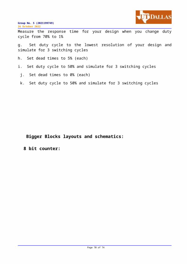
8 bit counter:
Page 70 of 74
Group No. 5 (2021199749)26 October 2022
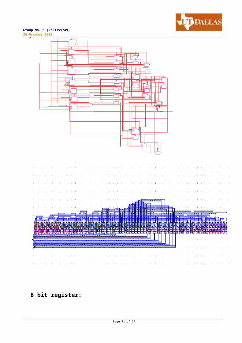
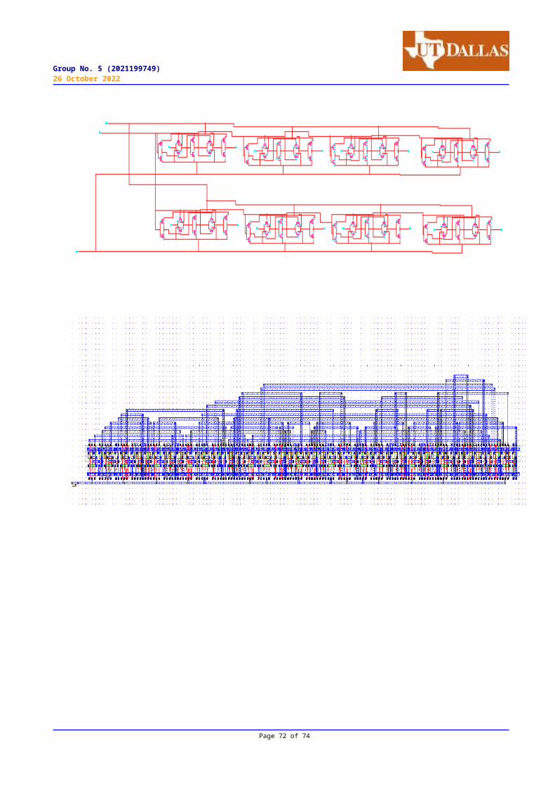
8 bit register:
Page 71 of 74
Group No. 5 (2021199749)26 October 2022
Page 72 of 74
Group No. 5 (2021199749)26 October 2022
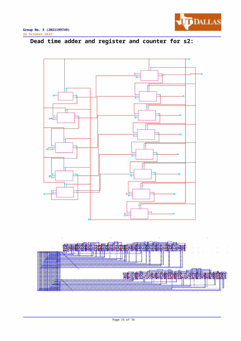
Dead time adder and register and counter for s2:
Page 73 of 74
Group No. 5 (2021199749)26 October 2022
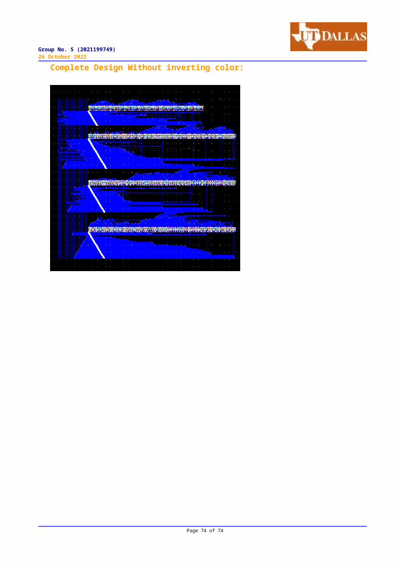
Complete Design Without inverting color:
Page 74 of 74


