Embed Size (px)
Citation preview
EE315B
VLSI Data Conversion Circuits
- Autumn 2013 -
Boris Murmann
Stanford University
Table of Contents
Chapter 1 Introduction
Chapter 2 Sampling, Reconstruction, Quantization
Chapter 3 Spectral Performance Metrics
Chapter 4 Nyquist Rate DACs
Chapter 5 Sampling Circuits
Chapter 6 Voltage Comparators
Chapter 7 Flash ADCs
Chapter 8 SAR ADCs
Chapter 9 Pipeline ADCs
Chapter 10 Time Interleaving
Chapter 11 Oversampling ADCs and DACs
Chapter 12 Energy Limits in A/D Converters

(This page is intentionally left blank)
B. Murmann 1EE315B - Chapter 1
Introduction
Boris Murmann
Stanford University
Copyright © 2013 by Boris Murmann
B. Murmann 2EE315B - Chapter 1
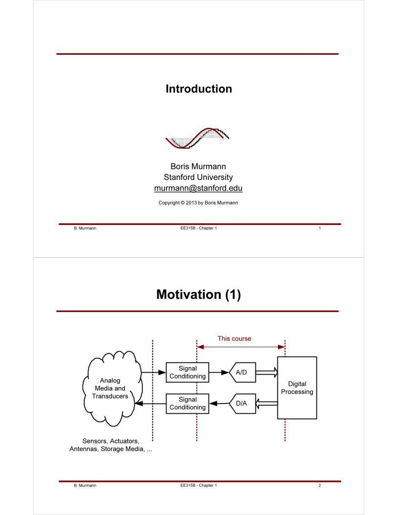
Motivation (1)
Digital
Processing
A/D
D/A
Signal
Conditioning
Signal
Conditioning
Analog
Media and
Transducers
Sensors, Actuators,
Antennas, Storage Media, ...
This course
B. Murmann 3EE315B - Chapter 1
Motivation (2)
• Benefits of digital signal processing
– Reduced sensitivity to "analog" noise
– Enhanced functionality and flexibility
– Amenable to automated design & test
– Direct benefit from the scaling of VLSI technology
– "Arbitrary" precision
• Issues
– Data converters are difficult to design
• Especially due to ever-increasing performance requirements
– Data converters often present a performance bottleneck
• Speed, resolution or power dissipation of the A/D or D/A
converter can limit overall system performance
B. Murmann 4
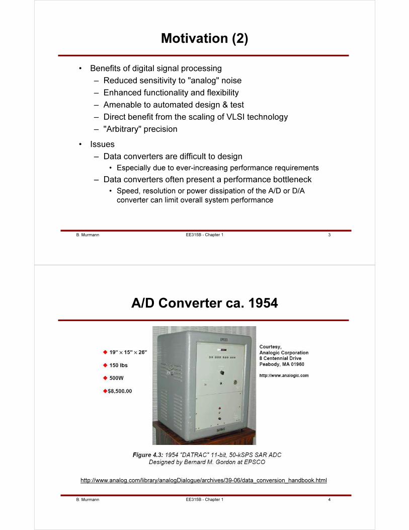
A/D Converter ca. 1954
http://www.analog.com/library/analogDialogue/archives/39-06/data_conversion_handbook.html
EE315B - Chapter 1
B. Murmann 5EE315B - Chapter 1
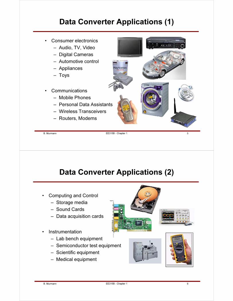
Data Converter Applications (1)
• Consumer electronics
– Audio, TV, Video
– Digital Cameras
– Automotive control
– Appliances
– Toys
• Communications
– Mobile Phones
– Personal Data Assistants
– Wireless Transceivers
– Routers, Modems
B. Murmann 6EE315B - Chapter 1
Data Converter Applications (2)
• Computing and Control
– Storage media
– Sound Cards
– Data acquisition cards
• Instrumentation
– Lab bench equipment
– Semiconductor test equipment
– Scientific equipment
– Medical equipment
B. Murmann 7EE315B - Chapter 1
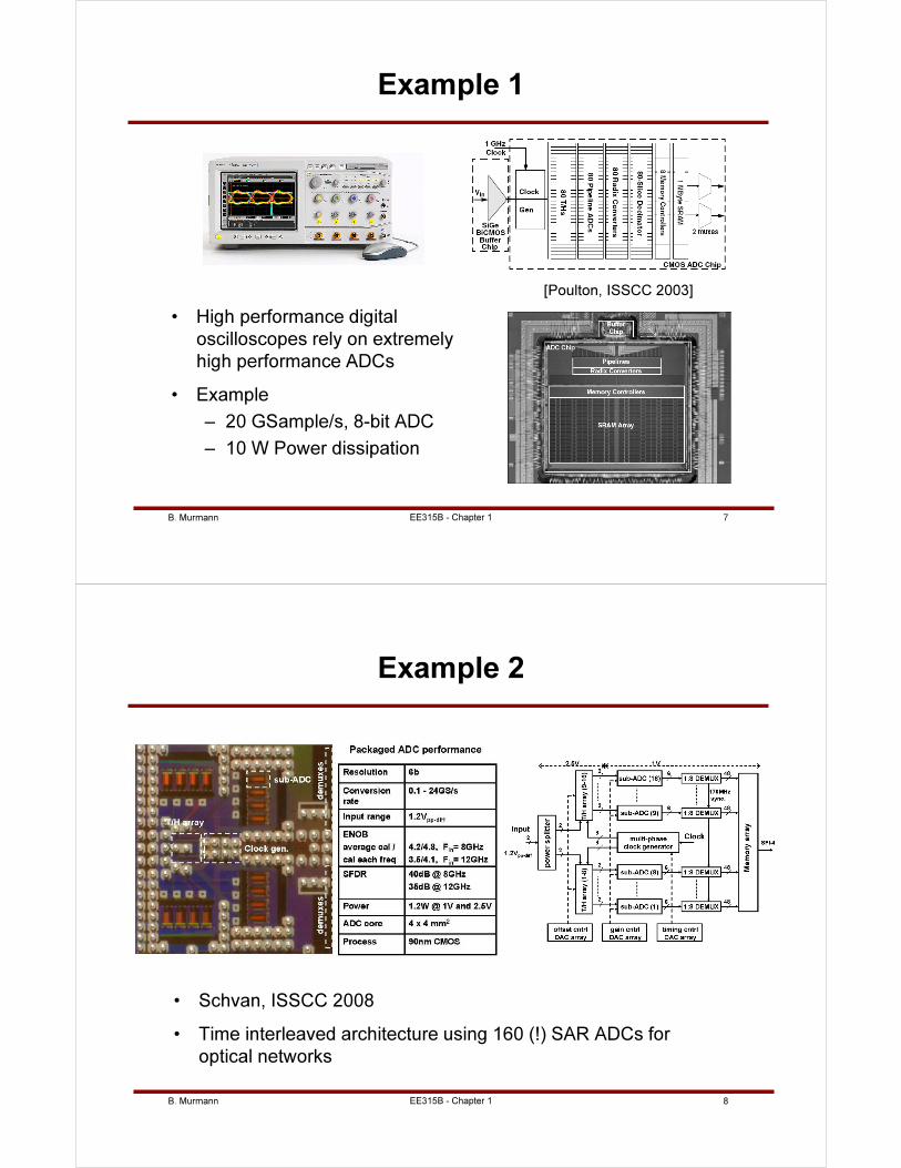
Example 1
• High performance digital
oscilloscopes rely on extremely
high performance ADCs
• Example
– 20 GSample/s, 8-bit ADC
– 10 W Power dissipation
[Poulton, ISSCC 2003]
B. Murmann 8
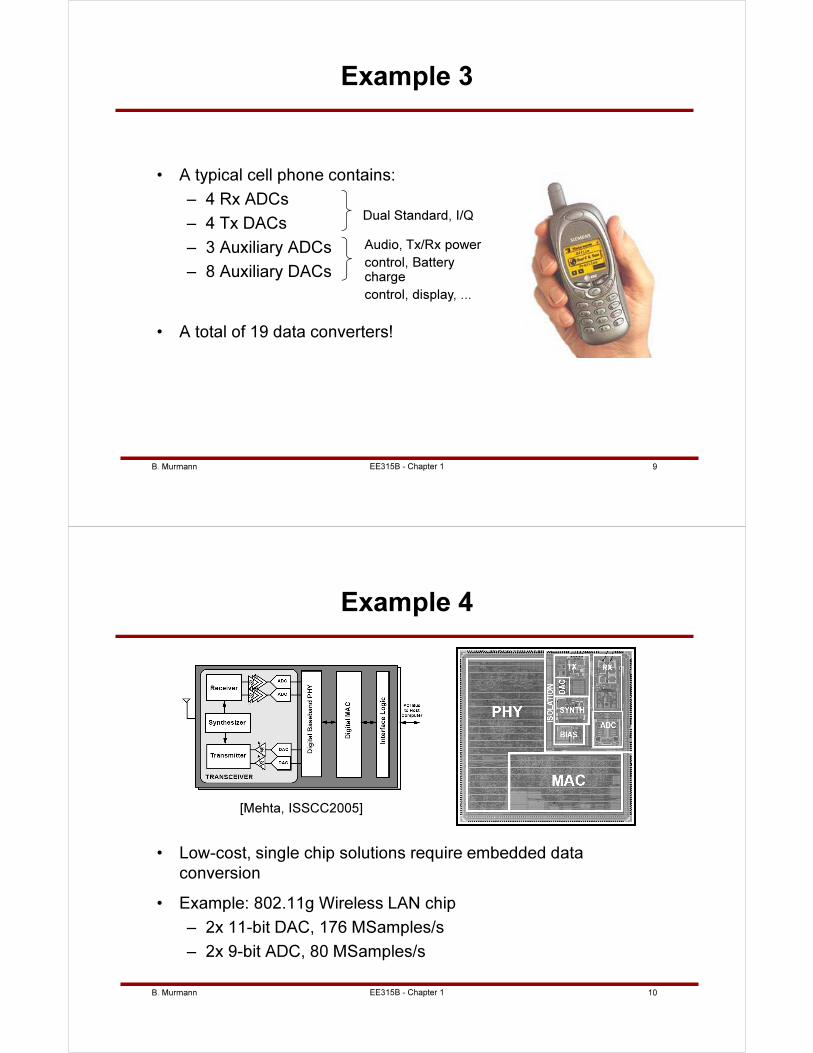
Example 2
• Schvan, ISSCC 2008
• Time interleaved architecture using 160 (!) SAR ADCs for
optical networks
EE315B - Chapter 1
B. Murmann 9EE315B - Chapter 1
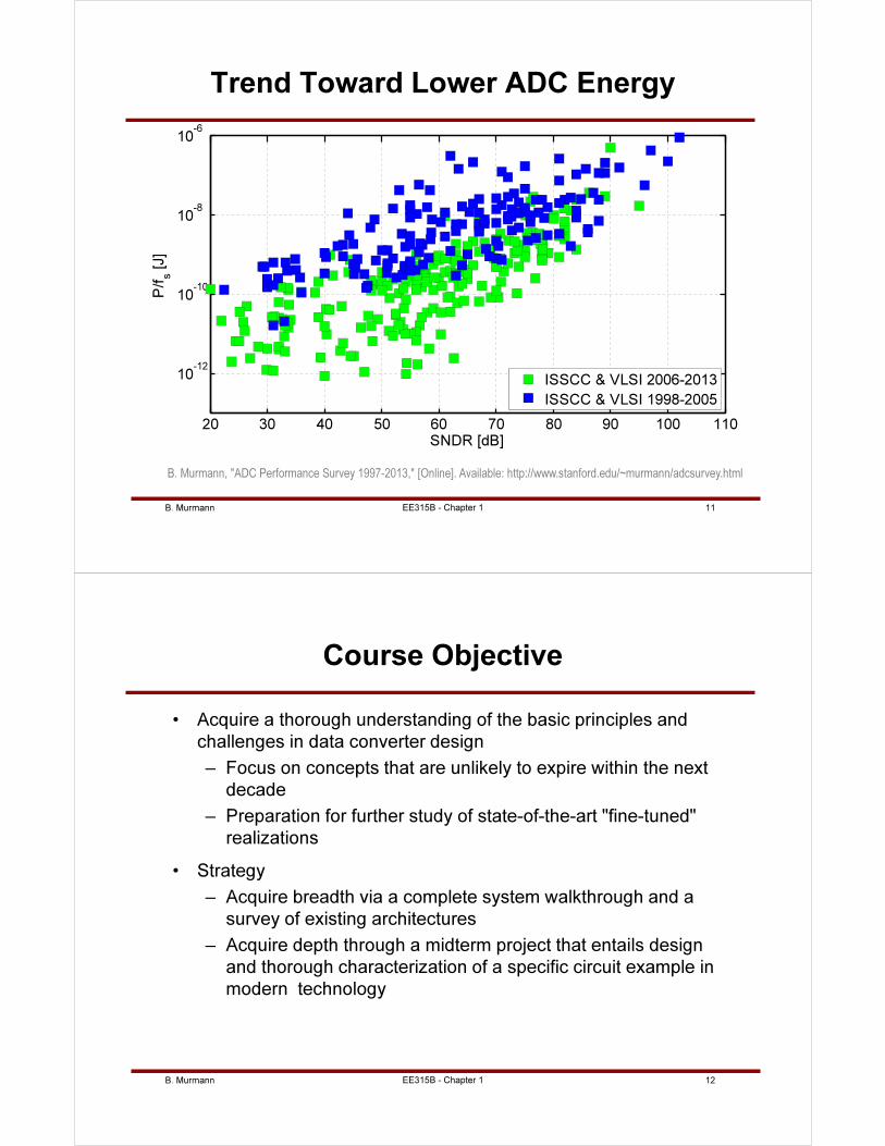
Example 3
• A typical cell phone contains:
– 4 Rx ADCs
– 4 Tx DACs
– 3 Auxiliary ADCs
– 8 Auxiliary DACs
• A total of 19 data converters!
Dual Standard, I/Q
Audio, Tx/Rx power
control, Battery charge
control, display, ...
B. Murmann 10EE315B - Chapter 1
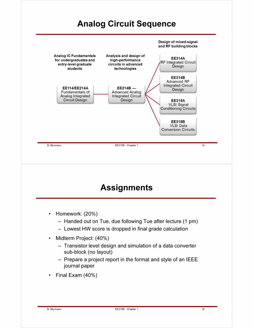
Example 4
• Low-cost, single chip solutions require embedded data
conversion
• Example: 802.11g Wireless LAN chip
– 2x 11-bit DAC, 176 MSamples/s
– 2x 9-bit ADC, 80 MSamples/s
[Mehta, ISSCC2005]
B. Murmann 11
Trend Toward Lower ADC Energy
EE315B - Chapter 1
B. Murmann, "ADC Performance Survey 1997-2013," [Online]. Available: http://www.stanford.edu/~murmann/adcsurvey.html
20 30 40 50 60 70 80 90 100 110
10-12
10-10
10-8
10-6
SNDR [dB]
P/fs [J]
ISSCC & VLSI 2006-2013
ISSCC & VLSI 1998-2005
B. Murmann 12EE315B - Chapter 1
Course Objective
• Acquire a thorough understanding of the basic principles and
challenges in data converter design
– Focus on concepts that are unlikely to expire within the next
decade
– Preparation for further study of state-of-the-art "fine-tuned"
realizations
• Strategy
– Acquire breadth via a complete system walkthrough and a
survey of existing architectures
– Acquire depth through a midterm project that entails design
and thorough characterization of a specific circuit example in
modern technology

B. Murmann 13EE315B - Chapter 1
Staff and Website
• Teaching assistant
– Vaibhav Tripathi
• Administrative support
– Ann Guerra, Allen 207
• Lecture videos are provided on the web, but please come to
class to keep the discussion intercative
• Coursework web page
– http://coursework.stanford.edu/homepage/F13/F13-EE-315B-01.html
– Please visit the discussion forum regularly
– Only enrolled students have full access
B. Murmann 14EE315B - Chapter 1
Preparation
• Course prerequisites
– EE214B or equivalent
• Device physics and models
• Transistor level analog circuits, elementary gain stages
• Frequency response, feedback, noise
– Prior exposure to Spice, Matlab
– Basic signals and systems
– Basic probability
• Please talk to me if you are not sure whether you have the
required background
B. Murmann 15
Analog Circuit Sequence
EE315B - Chapter 1
B. Murmann 16EE315B - Chapter 1
Assignments
• Homework: (20%)
– Handed out on Tue, due following Tue after lecture (1 pm)
– Lowest HW score is dropped in final grade calculation
• Midterm Project: (40%)
– Transistor level design and simulation of a data converter
sub-block (no layout)
– Prepare a project report in the format and style of an IEEE
journal paper
• Final Exam (40%)

B. Murmann 17EE315B - Chapter 1
Honor Code
• Please remember you are bound by the honor code
– I will trust you not to cheat
– I will try not to tempt you
• But if you are found cheating it is very serious
– There is a formal hearing
– You can be thrown out of Stanford
• Save yourself and me a huge hassle and be honest
• For more info
– http://www.stanford.edu/dept/vpsa/judicialaffairs/guiding/pdf/
honorcode.pdf
B. Murmann 18EE315B - Chapter 1
Tools and Technology
• Primary tools
– Cadence Virtuoso Schematic Editor
– Cadence Virtuoso Analog Design Environment
– Cadence SpectreRF simulator
– You can use your own tools/setups “at own risk“
• Getting started
– Read tutorials and setup info provided in the CAD section of the
course website
• EE315A/B Technology
– 0.18-µm CMOS
– BSIM3v3 models provided under /usr/class/ee315b/models
B. Murmann 19EE315B - Chapter 1
Reference Books
• M. Pelgrom, Analog-to-Digital Conversion, Springer, 2010
• Gustavsson, Wikner, Tan, CMOS Data Converters for
Communications, Kluwer, 2000
• A. Rodríguez-Vázquez, F. Medeiro, and E. Janssens, CMOS Telecom
Data Converters, Kluwer Academic Publishers, 2003
• W. Kester, The Data Conversion Handbook, Newnes, 2005http://www.analog.com/library/analogdialogue/archives/39-06/data_conversion_handbook.html
• B. Razavi, Data Conversion System Design, IEEE Press, 1995
• R. Schreier, G. Temes, Understanding Delta-Sigma Data Converters,
Wiley-IEEE Press, 2004
• R. v. d. Plassche, CMOS Integrated Analog-to-Digital and Digital-to-
Analog Converters, 2nd ed., Kluwer, 2003
• J. G. Proakis, and D. G. Manolakis, Digital Signal Processing,
Prentice Hall, 1995
B. Murmann 20EE315B - Chapter 1
Course Topics
• Ideal sampling, reconstruction and quantization
• Sampling circuits
• Voltage comparators
• Nyquist-rate ADCs and DACs
• Oversampled ADCs and DACs
• Data converter performance trends and limits
• Data converter testing, simulation techniques
B. Murmann 1EE315B - Chapter 2
Sampling, Reconstruction, Quantization
Boris Murmann
Stanford University
Copyright © 2013 by Boris Murmann
B. Murmann 2EE315B - Chapter 2
The Data Conversion Problem
• Real world signals
– Continuous time, continuous amplitude
• Digital abstraction
– Discrete time, discrete amplitude
• Two problems
– How to discretize in time and amplitude
• A/D conversion
– How to "undescretize" in time and amplitude
• D/A conversion
B. Murmann 3EE315B - Chapter 2
Overview
• We'll fist look at these building blocks from a functional, "black
box" perspective
– Refine later and look at implementations
B. Murmann 4EE315B - Chapter 2
Uniform Sampling and Quantization
• Most common way of performing A/D
conversion
– Sample signal uniformly in time
– Quantize signal uniformly in
amplitude
• Key questions
– How much "noise" is added due
to amplitude quantization?
– How can we reconstruct the
signal back into analog form?
– How fast do we need to sample?
• Must avoid "aliasing"
B. Murmann 5EE315B - Chapter 2
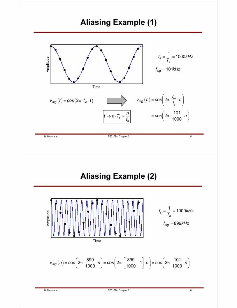
Aliasing Example (1)
11000
101
ss
sig
f kHzT
f kHz
= =
=
( ) ( )2sig inv t cos f t= π ⋅ ⋅ ( ) 2
1012
1000
insig
s
fv n cos n
f
cos n
= π ⋅ ⋅
= π ⋅ ⋅
s
s
nt n T
f→ ⋅ =
Time
Amplitude
B. Murmann 6EE315B - Chapter 2
Aliasing Example (2)
11000
899
ss
sig
f kHzT
f kHz
= =
=
( )899 899 101
2 2 1 21000 1000 1000
sigv n cos n cos n cos n
= π ⋅ ⋅ = π ⋅ − ⋅ = π ⋅ ⋅
Time
Amplitude
B. Murmann 7EE315B - Chapter 2
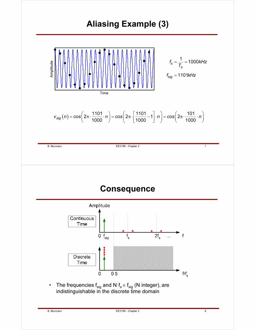
Aliasing Example (3)
11000
1101
ss
sig
f kHzT
f kHz
= =
=
( )1101 1101 101
2 2 1 21000 1000 1000
sigv n cos n cos n cos n
= π ⋅ ⋅ = π ⋅ − ⋅ = π ⋅ ⋅
Time
Amplitude
B. Murmann 8EE315B - Chapter 2
Consequence
• The frequencies fsig and N·fs ± fsig (N integer), are
indistinguishable in the discrete time domain
B. Murmann 9EE315B - Chapter 2
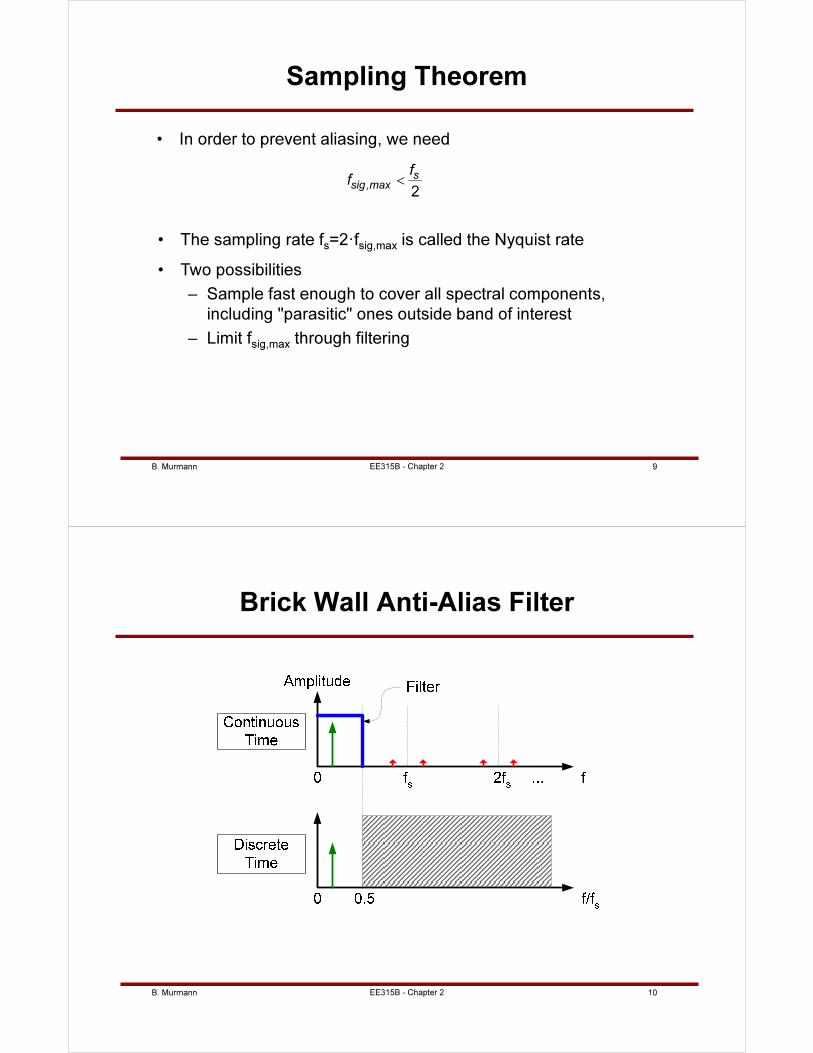
Sampling Theorem
• In order to prevent aliasing, we need
2
ssig,max
ff <
• The sampling rate fs=2·fsig,max is called the Nyquist rate
• Two possibilities
– Sample fast enough to cover all spectral components,
including "parasitic" ones outside band of interest
– Limit fsig,max through filtering
B. Murmann 10EE315B - Chapter 2
Brick Wall Anti-Alias Filter
B. Murmann 11EE315B - Chapter 2
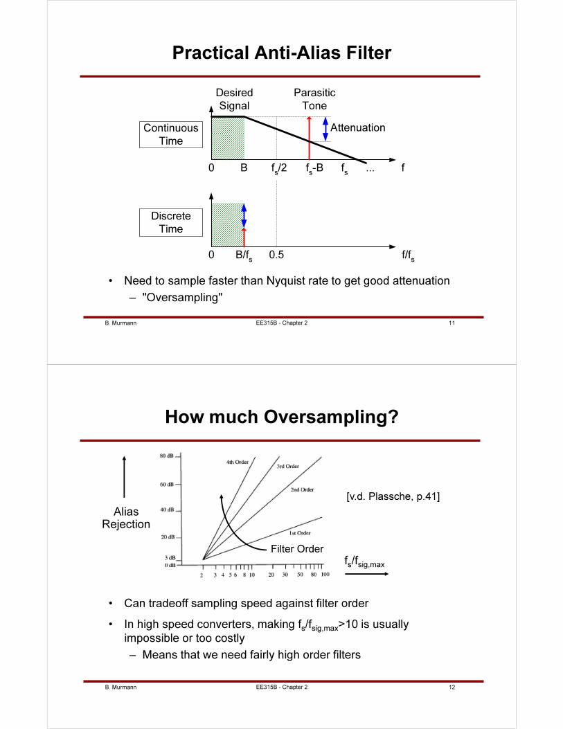
Practical Anti-Alias Filter
• Need to sample faster than Nyquist rate to get good attenuation
– "Oversampling"
Continuous
Time
Discrete
Time
0 fs
... f
Desired
Signal
0 0.5 f/fs
fs/2B f
s-B
Parasitic
Tone
B/fs
Attenuation
B. Murmann 12EE315B - Chapter 2
How much Oversampling?
• Can tradeoff sampling speed against filter order
• In high speed converters, making fs/fsig,max>10 is usually
impossible or too costly
– Means that we need fairly high order filters
Alias Rejection
fs/fsig,max
Filter Order
[v.d. Plassche, p.41]
B. Murmann 13EE315B - Chapter 2
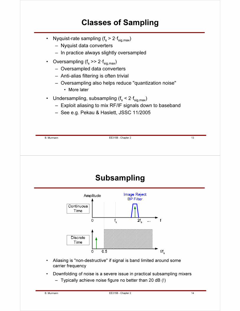
Classes of Sampling
• Nyquist-rate sampling (fs > 2·fsig,max)
– Nyquist data converters
– In practice always slightly oversampled
• Oversampling (fs >> 2·fsig,max)
– Oversampled data converters
– Anti-alias filtering is often trivial
– Oversampling also helps reduce "quantization noise"
• More later
• Undersampling, subsampling (fs < 2·fsig,max)
– Exploit aliasing to mix RF/IF signals down to baseband
– See e.g. Pekau & Haslett, JSSC 11/2005
B. Murmann 14EE315B - Chapter 2
Subsampling
• Aliasing is "non-destructive" if signal is band limited around some
carrier frequency
• Downfolding of noise is a severe issue in practical subsampling mixers
– Typically achieve noise figure no better than 20 dB (!)
B. Murmann 15EE315B - Chapter 2
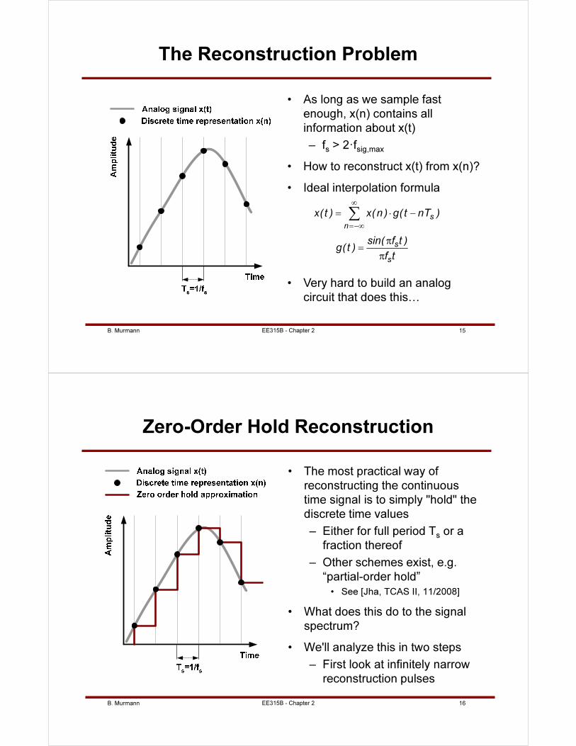
The Reconstruction Problem
• As long as we sample fast
enough, x(n) contains all
information about x(t)
– fs > 2·fsig,max
• How to reconstruct x(t) from x(n)?
• Ideal interpolation formula
s
n
x(t ) x(n ) g( t nT )∞
=−∞
= ⋅ −∑
s
s
sin( f t )g( t )
f t
π
=
π
• Very hard to build an analog
circuit that does this…
B. Murmann 16EE315B - Chapter 2
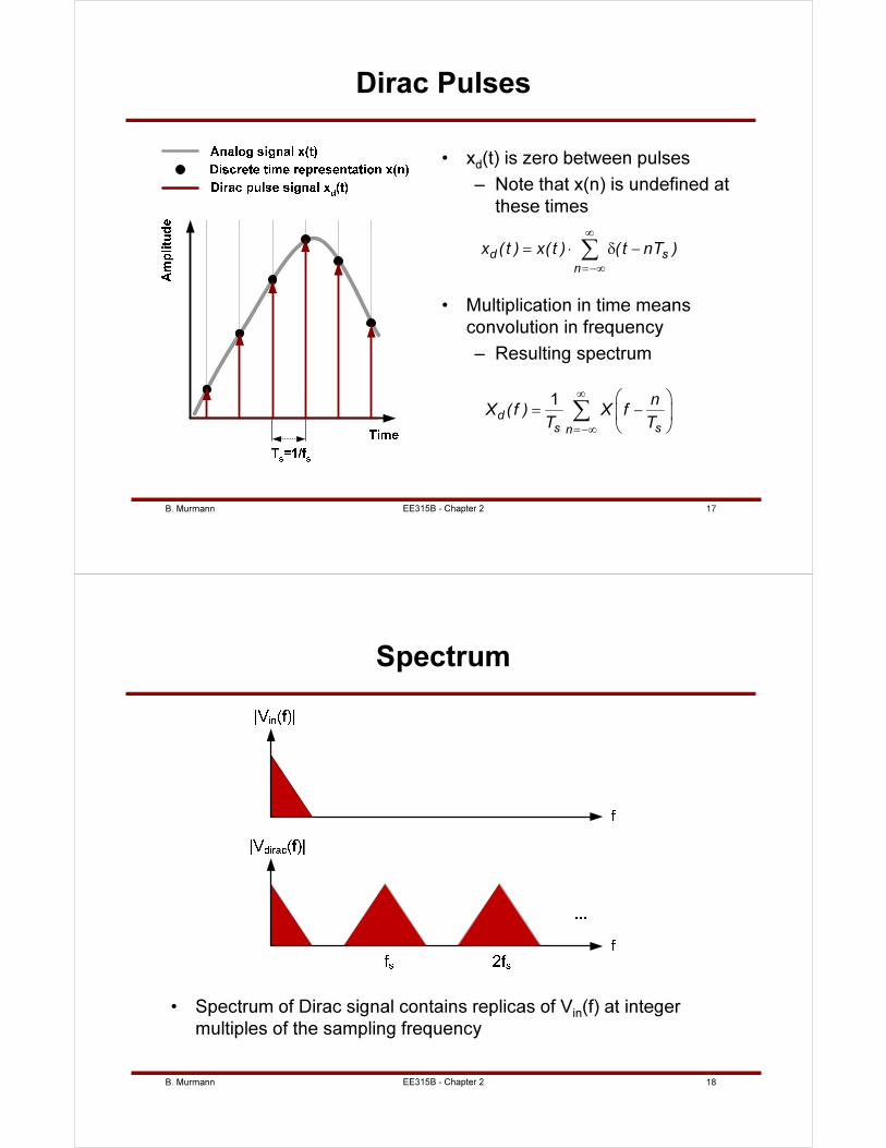
Zero-Order Hold Reconstruction
• The most practical way of
reconstructing the continuous
time signal is to simply "hold" the
discrete time values
– Either for full period Ts or a
fraction thereof
– Other schemes exist, e.g.
“partial-order hold”
• See [Jha, TCAS II, 11/2008]
• What does this do to the signal
spectrum?
• We'll analyze this in two steps
– First look at infinitely narrow
reconstruction pulses
B. Murmann 17EE315B - Chapter 2
Dirac Pulses
• xd(t) is zero between pulses
– Note that x(n) is undefined at
these times
d s
n
x ( t ) x( t ) ( t nT )∞
=−∞
= ⋅ δ −∑
1d
s sn
nX (f ) X f
T T
∞
=−∞
= −
∑
• Multiplication in time means
convolution in frequency
– Resulting spectrum
B. Murmann 18EE315B - Chapter 2
Spectrum
• Spectrum of Dirac signal contains replicas of Vin(f) at integer
multiples of the sampling frequency
B. Murmann 19EE315B - Chapter 2
Finite Hold Pulse
• Consider the general case with a
rectangular pulse 0 < Tp ≤ Ts
• The time domain signal on the left
follows from convolving the Dirac
sequence with a rectangular unit pulse
• Spectrum follows from multiplication with
Fourier transform of the pulse
pj fTpp p
p
sin( fT )H (f ) T e
fT
− ππ
= ⋅
π
pj fTp pp
s p sn
T sin( fT ) nX (f ) e X f
T fT T
∞
− π
=−∞
π = ⋅ −
π ∑
Amplitude Envelope
B. Murmann 20EE315B - Chapter 2
Envelope with Hold Pulse Tp=T
s
0 0.5 1 1.5 2 2.5 30
0.1
0.2
0.3
0.4
0.5
0.6
0.7
0.8
0.9
1
f/fs
abs(H(f))
f/fs
p p
s p
T sin( fT )
T fT
π
π
B. Murmann 21EE315B - Chapter 2
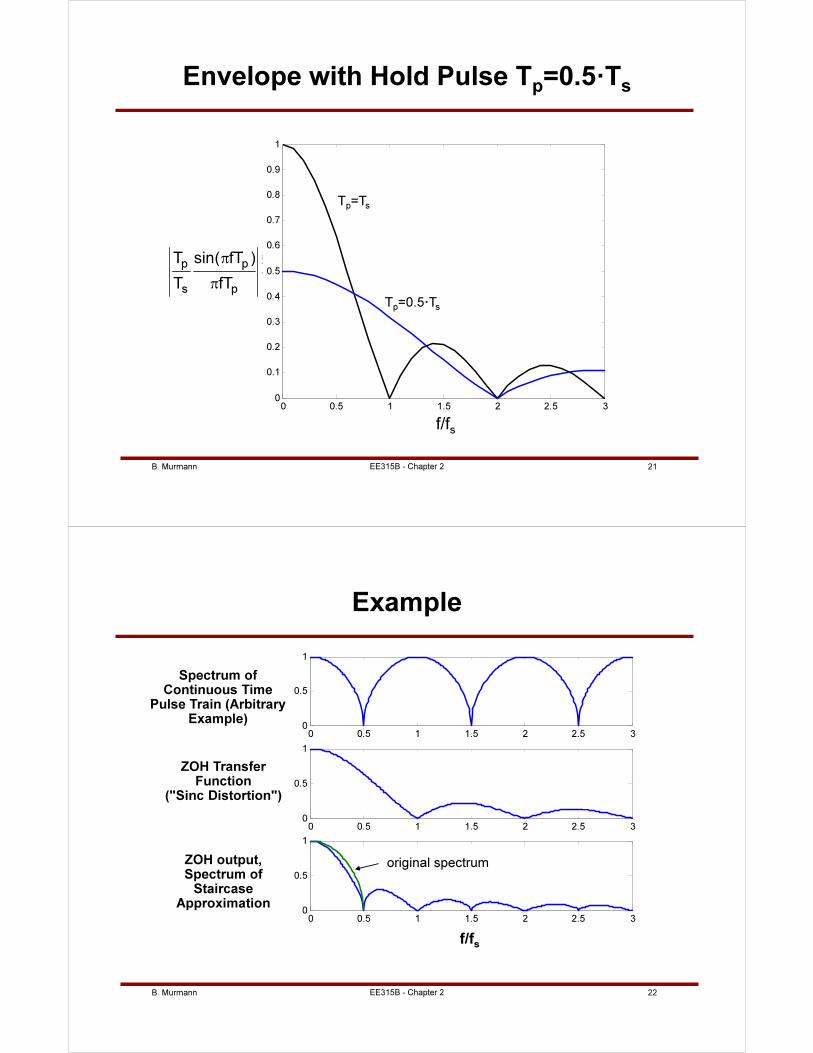
Envelope with Hold Pulse Tp=0.5·T
s
0 0.5 1 1.5 2 2.5 30
0.1
0.2
0.3
0.4
0.5
0.6
0.7
0.8
0.9
1
f/fs
abs(H(f))
f/fs
p p
s p
T sin( fT )
T fT
π
π
Tp=Ts
Tp=0.5·Ts
B. Murmann 22EE315B - Chapter 2
Example
Spectrum of Continuous Time
Pulse Train (Arbitrary Example)
ZOH Transfer Function
("Sinc Distortion")
ZOH output, Spectrum of
Staircase Approximation
0 0.5 1 1.5 2 2.5 30
0.5
1
0 0.5 1 1.5 2 2.5 30
0.5
1
0 0.5 1 1.5 2 2.5 30
0.5
1
f/fs
original spectrum
B. Murmann 23EE315B - Chapter 2
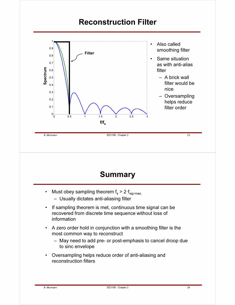
Reconstruction Filter
• Also called
smoothing filter
• Same situation
as with anti-alias
filter
– A brick wall
filter would be
nice
– Oversampling
helps reduce
filter order
0 0.5 1 1.5 2 2.5 30
0.1
0.2
0.3
0.4
0.5
0.6
0.7
0.8
0.9
1
f/fs
Spectrum
Filter
B. Murmann 24EE315B - Chapter 2
Summary
• Must obey sampling theorem fs > 2·fsig,max,
– Usually dictates anti-aliasing filter
• If sampling theorem is met, continuous time signal can be
recovered from discrete time sequence without loss of
information
• A zero order hold in conjunction with a smoothing filter is the
most common way to reconstruct
– May need to add pre- or post-emphasis to cancel droop due
to sinc envelope
• Oversampling helps reduce order of anti-aliasing and
reconstruction filters
B. Murmann 25EE315B - Chapter 2
Recap
• Next, look at
– Transfer functions of quantizer and DAC
– Impact of quantization error
B. Murmann 26EE315B - Chapter 2
Quantization of an Analog Signal
• Quantization step ∆
• Quantization error has sawtooth shape
– Bounded by –∆/2, +∆/2
• Ideally
– Infinite input range and infinite number of quantization levels
• In practice
– Finite input range and finite number of quantization levels
– Output is a digital word (not an analog voltage)
+∆/2
-∆/2
x (input)
eq (
qu
an
tiza
tio
n e
rro
r)
Error eq=q-x
x (input)
Vq
(quantized o
utp
ut)
Transfer Function
∆
Slope=1
B. Murmann 27EE315B - Chapter 2
Conceptual Model of a Quantizer
• Encoding block determines how quantized levels are mapped
into digital codes
• Note that this model is not meant to represent an actual
hardware implementation
– Its purpose is to show that quantization and encoding are
conceptually separate operations
– Changing the encoding of a quantizer has no interesting
implications on its function or performance
B. Murmann 28EE315B - Chapter 2
+∆/2
-∆/2
x (input)
eq (
qu
an
tiza
tio
n e
rro
r)
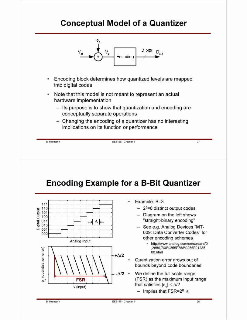
Encoding Example for a B-Bit Quantizer
• Example: B=3
– 23=8 distinct output codes
– Diagram on the left shows
"straight-binary encoding"
– See e.g. Analog Devices "MT-
009: Data Converter Codes" for
other encoding schemes• http://www.analog.com/en/content/0
,2886,760%255F788%255F91285,
00.html
• Quantization error grows out of
bounds beyond code boundaries
• We define the full scale range
(FSR) as the maximum input range
that satisfies |eq| ≤ ∆/2
– Implies that FSR=2B·∆
000
001
010
011
100
101
110
111
Analog Input
Dig
ita
l O
utp
ut
∆
FSR
B. Murmann 29EE315B - Chapter 2
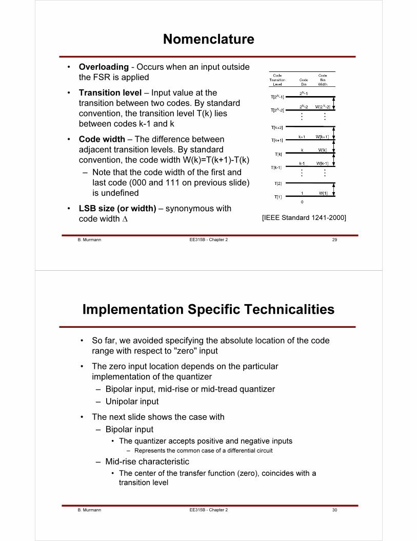
Nomenclature
• Overloading - Occurs when an input outside
the FSR is applied
• Transition level – Input value at the
transition between two codes. By standard
convention, the transition level T(k) lies
between codes k-1 and k
• Code width – The difference between
adjacent transition levels. By standard
convention, the code width W(k)=T(k+1)-T(k)
– Note that the code width of the first and
last code (000 and 111 on previous slide)
is undefined
• LSB size (or width) – synonymous with
code width ∆ [IEEE Standard 1241-2000]
B. Murmann 30EE315B - Chapter 2
Implementation Specific Technicalities
• So far, we avoided specifying the absolute location of the code
range with respect to "zero" input
• The zero input location depends on the particular
implementation of the quantizer
– Bipolar input, mid-rise or mid-tread quantizer
– Unipolar input
• The next slide shows the case with
– Bipolar input
• The quantizer accepts positive and negative inputs– Represents the common case of a differential circuit
– Mid-rise characteristic
• The center of the transfer function (zero), coincides with a
transition level
B. Murmann 31EE315B - Chapter 2
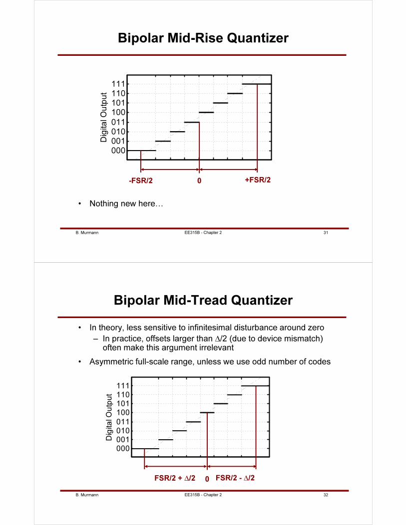
Bipolar Mid-Rise Quantizer
• Nothing new here…
000001010011
100101110111
Analog Input
Dig
ita
l O
utp
ut
0-FSR/2 +FSR/2
B. Murmann 32EE315B - Chapter 2
Bipolar Mid-Tread Quantizer
• In theory, less sensitive to infinitesimal disturbance around zero
– In practice, offsets larger than ∆/2 (due to device mismatch) often make this argument irrelevant
• Asymmetric full-scale range, unless we use odd number of codes
000001010011
100101110111
Analog Input
Dig
ita
l O
utp
ut
0 FSR/2 - ∆/2FSR/2 + ∆/2
B. Murmann 33EE315B - Chapter 2
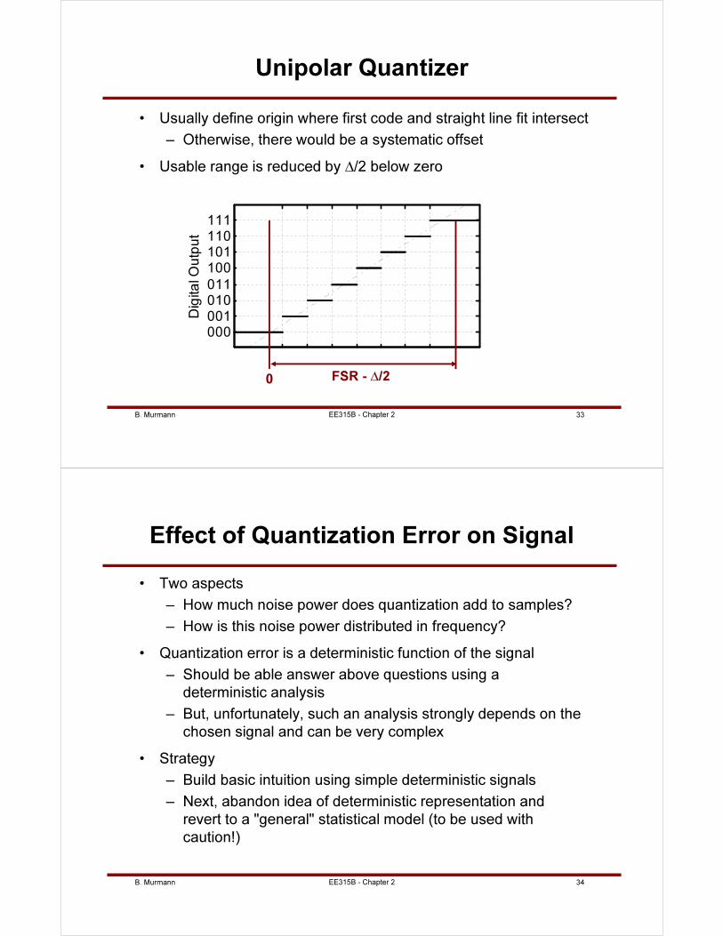
Unipolar Quantizer
• Usually define origin where first code and straight line fit intersect
– Otherwise, there would be a systematic offset
• Usable range is reduced by ∆/2 below zero
000001010011
100101110111
Analog Input
Dig
ita
l O
utp
ut
0 FSR - ∆/2
B. Murmann 34EE315B - Chapter 2
Effect of Quantization Error on Signal
• Two aspects
– How much noise power does quantization add to samples?
– How is this noise power distributed in frequency?
• Quantization error is a deterministic function of the signal
– Should be able answer above questions using a
deterministic analysis
– But, unfortunately, such an analysis strongly depends on the
chosen signal and can be very complex
• Strategy
– Build basic intuition using simple deterministic signals
– Next, abandon idea of deterministic representation and
revert to a "general" statistical model (to be used with
caution!)
B. Murmann 35EE315B - Chapter 2
Ramp Input
• Applying a ramp signal (periodic sawtooth) at the input of the
quantizer gives the following time domain waveform for eq
• What is the average power of this waveform?
• Integrate over one period
2
2 2
2
1T /
q q
T /
e e (t )dtT
−
= ∫ qe (t ) tT
∆= ⋅
22
12qe
∆∴ =
0 50 100 150
-0.4
-0.2
0
0.2
0.4
0.6
Time [arbitrary units]
eq(t
) [ ∆
]
B. Murmann 36EE315B - Chapter 2
Sine Wave Input
• Integration is not straightforward…
0 0.2 0.4 0.6 0.8 1-1
-0.8
-0.6
-0.4
-0.2
0
0.2
0.4
0.6
0.8
1
Time [arbitrary units]
[Vo
lts]
0 0.2 0.4 0.6 0.8 1-1
-0.8
-0.6
-0.4
-0.2
0
0.2
0.4
0.6
0.8
1
Time [arbitrary units]
eq(t
) [ ∆
]
Vin
Vq
B. Murmann 37EE315B - Chapter 2
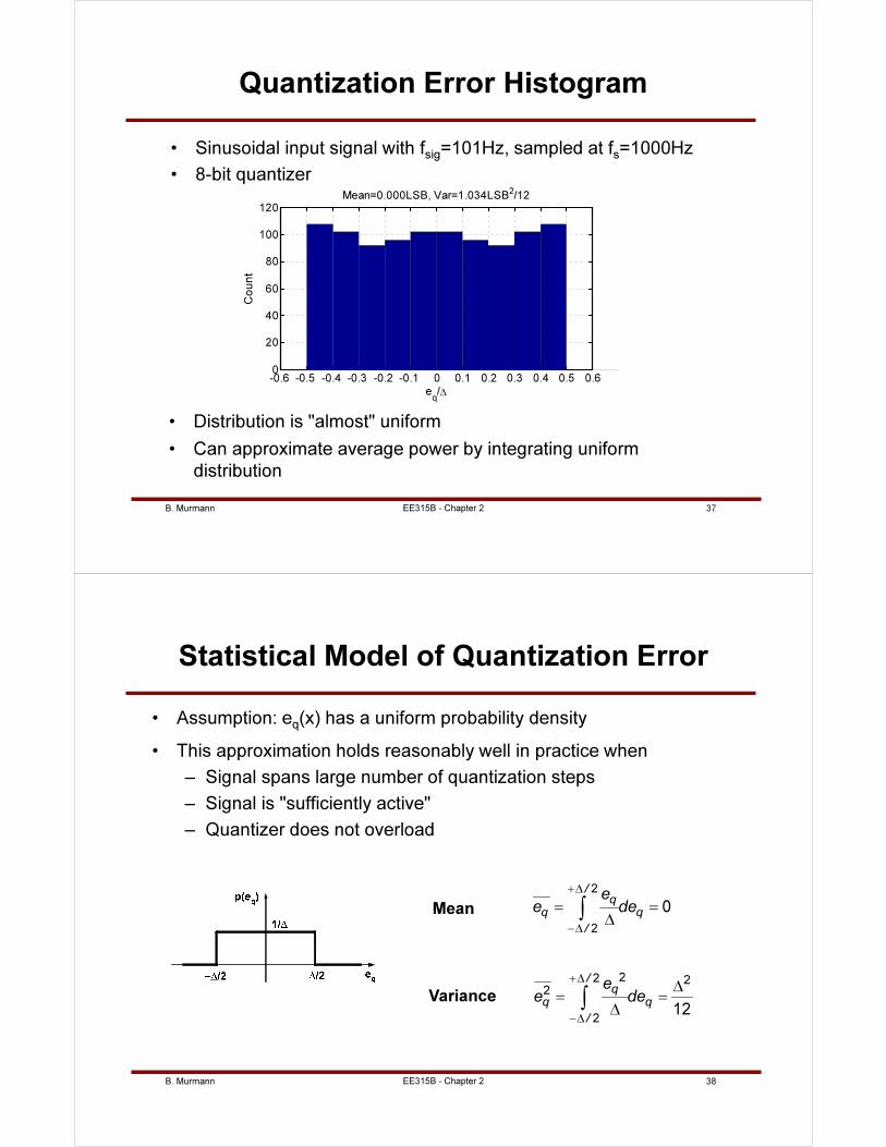
Quantization Error Histogram
• Sinusoidal input signal with fsig=101Hz, sampled at fs=1000Hz
• 8-bit quantizer
-0.6 -0.5 -0.4 -0.3 -0.2 -0.1 0 0.1 0.2 0.3 0.4 0.5 0.60
20
40
60
80
100
120
Mean=0.000LSB, Var=1.034LSB2/12
eq/∆
Count
• Distribution is "almost" uniform
• Can approximate average power by integrating uniform
distribution
B. Murmann 38EE315B - Chapter 2
Statistical Model of Quantization Error
• Assumption: eq(x) has a uniform probability density
• This approximation holds reasonably well in practice when
– Signal spans large number of quantization steps
– Signal is "sufficiently active"
– Quantizer does not overload
22 22
212
/q
q q
/
ee de
+∆
−∆
∆= =
∆∫
2
2
0
/q
q q
/
ee de
+∆
−∆
= =∆
∫Mean
Variance
B. Murmann 39EE315B - Chapter 2
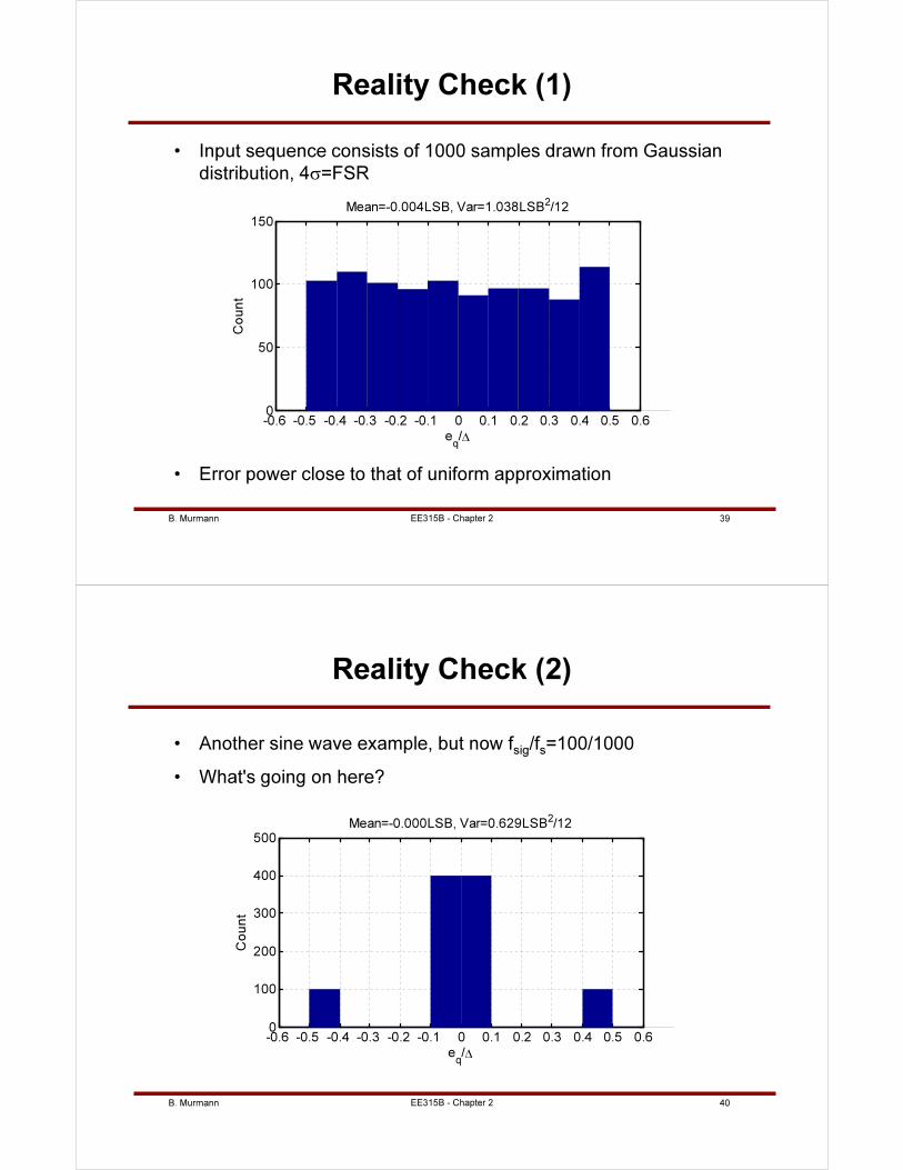
Reality Check (1)
• Input sequence consists of 1000 samples drawn from Gaussian
distribution, 4σ=FSR
-0.6 -0.5 -0.4 -0.3 -0.2 -0.1 0 0.1 0.2 0.3 0.4 0.5 0.60
50
100
150
Mean=-0.004LSB, Var=1.038LSB2/12
eq/∆
Count
• Error power close to that of uniform approximation
B. Murmann 40EE315B - Chapter 2
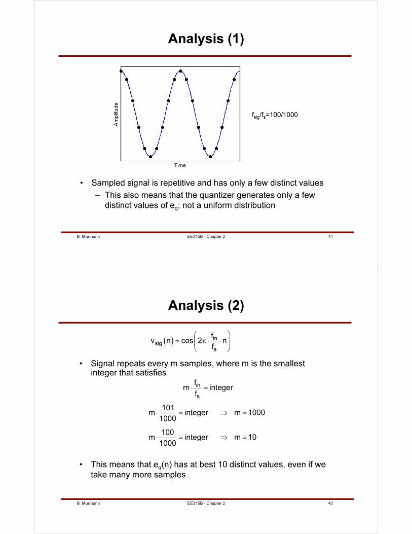
Reality Check (2)
• Another sine wave example, but now fsig/fs=100/1000
• What's going on here?
-0.6 -0.5 -0.4 -0.3 -0.2 -0.1 0 0.1 0.2 0.3 0.4 0.5 0.60
100
200
300
400
500
Mean=-0.000LSB, Var=0.629LSB2/12
eq/∆
Count
B. Murmann 41EE315B - Chapter 2
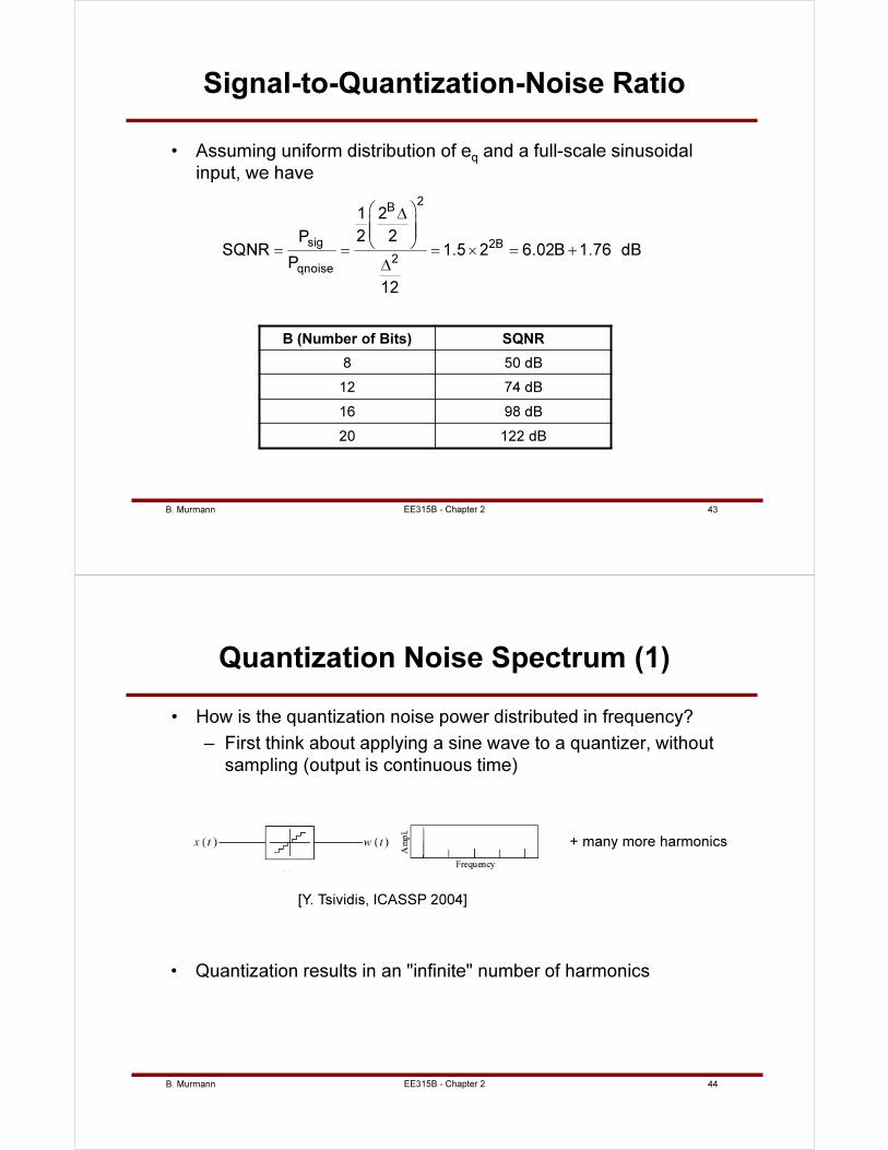
Analysis (1)
• Sampled signal is repetitive and has only a few distinct values
– This also means that the quantizer generates only a few
distinct values of eq; not a uniform distribution
Time
Amplitude
fsig/fs=100/1000
B. Murmann 42EE315B - Chapter 2
Analysis (2)
( ) insig
s
fv n cos 2 n
f
= π ⋅ ⋅
• Signal repeats every m samples, where m is the smallest integer that satisfies
in
s
fm integer
f⋅ =
101m integer m 1000
1000
100m integer m 10
1000
⋅ = ⇒ =
⋅ = ⇒ =
• This means that eq(n) has at best 10 distinct values, even if we
take many more samples
B. Murmann 43EE315B - Chapter 2
Signal-to-Quantization-Noise Ratio
• Assuming uniform distribution of eq and a full-scale sinusoidal
input, we have
2B
sig 2B
2qnoise
1 2
2 2PSQNR 1.5 2 6.02B 1.76 dB
P
12
∆ = = = × = +∆
B (Number of Bits) SQNR
8 50 dB
12 74 dB
16 98 dB
20 122 dB
B. Murmann 44EE315B - Chapter 2
Quantization Noise Spectrum (1)
[Y. Tsividis, ICASSP 2004]
• How is the quantization noise power distributed in frequency?
– First think about applying a sine wave to a quantizer, without
sampling (output is continuous time)
+ many more harmonics
• Quantization results in an "infinite" number of harmonics
B. Murmann 45EE315B - Chapter 2
Quantization Noise Spectrum (2)
[Y. Tsividis, ICASSP 2004]
• Now sample the signal at the output
– All harmonics (an "infinite" number of them) will alias into
band from 0 to fs/2
– Quantization noise spectrum becomes "white"
• Interchanging sampling and quantization won’t change this
situation
B. Murmann 46EE315B - Chapter 2
Quantization Noise Spectrum (3)
• Can show that the quantization noise power is indeed distributed (approximately) uniformly in frequency
– Again, this is provided that the quantization error is "sufficiently random"
• References
– W. R. Bennett, "Spectra of quantized signals," Bell Syst. Tech. J., pp. 446-72,
July 1948.
– B. Widrow, "A study of rough amplitude quantization by means of Nyquist
sampling theory," IRE Trans. Circuit Theory, vol. CT-3, pp. 266-76, 1956.
– A. Sripad and D. A. Snyder, "A necessary and sufficient condition for
quantization errors to be uniform and white," IEEE Trans. Acoustics, Speech,
and Signal Processing, pp. 442-448, Oct 1977.
22
12sf
∆⋅
B. Murmann 47EE315B - Chapter 2
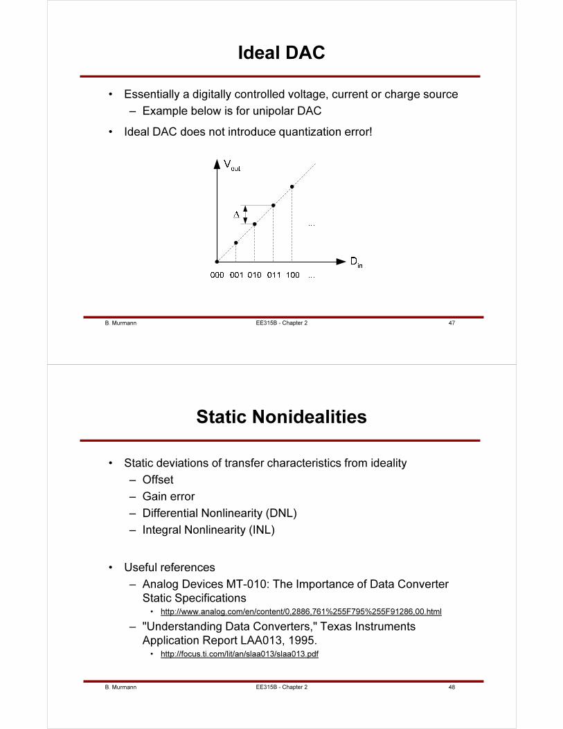
Ideal DAC
• Essentially a digitally controlled voltage, current or charge source
– Example below is for unipolar DAC
• Ideal DAC does not introduce quantization error!
B. Murmann 48EE315B - Chapter 2
Static Nonidealities
• Static deviations of transfer characteristics from ideality
– Offset
– Gain error
– Differential Nonlinearity (DNL)
– Integral Nonlinearity (INL)
• Useful references
– Analog Devices MT-010: The Importance of Data Converter
Static Specifications• http://www.analog.com/en/content/0,2886,761%255F795%255F91286,00.html
– "Understanding Data Converters," Texas Instruments
Application Report LAA013, 1995.• http://focus.ti.com/lit/an/slaa013/slaa013.pdf
B. Murmann 49EE315B - Chapter 2
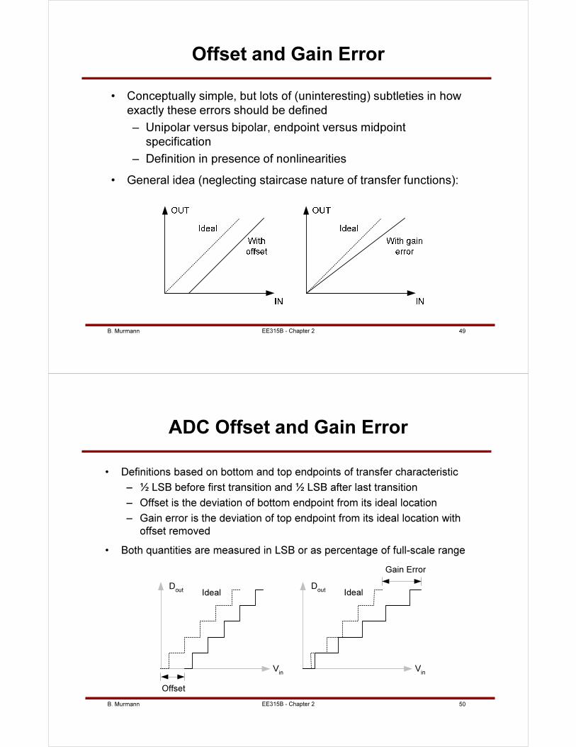
Offset and Gain Error
• Conceptually simple, but lots of (uninteresting) subtleties in how
exactly these errors should be defined
– Unipolar versus bipolar, endpoint versus midpoint
specification
– Definition in presence of nonlinearities
• General idea (neglecting staircase nature of transfer functions):
B. Murmann 50EE315B - Chapter 2
ADC Offset and Gain Error
• Definitions based on bottom and top endpoints of transfer characteristic
– ½ LSB before first transition and ½ LSB after last transition
– Offset is the deviation of bottom endpoint from its ideal location
– Gain error is the deviation of top endpoint from its ideal location with
offset removed
• Both quantities are measured in LSB or as percentage of full-scale range
Dout
Vin
Ideal
Offset
Dout
Vin
Ideal
Gain Error
B. Murmann 51EE315B - Chapter 2
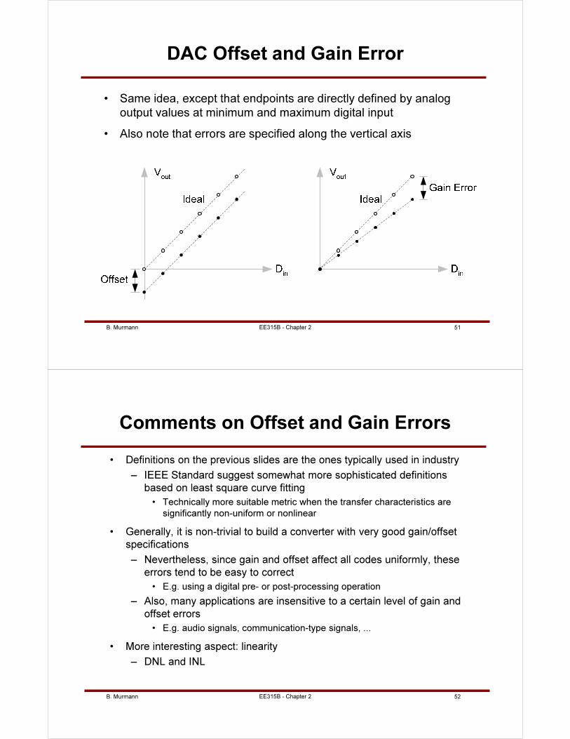
DAC Offset and Gain Error
• Same idea, except that endpoints are directly defined by analog
output values at minimum and maximum digital input
• Also note that errors are specified along the vertical axis
B. Murmann 52EE315B - Chapter 2
Comments on Offset and Gain Errors
• Definitions on the previous slides are the ones typically used in industry
– IEEE Standard suggest somewhat more sophisticated definitions
based on least square curve fitting
• Technically more suitable metric when the transfer characteristics are
significantly non-uniform or nonlinear
• Generally, it is non-trivial to build a converter with very good gain/offset
specifications
– Nevertheless, since gain and offset affect all codes uniformly, these
errors tend to be easy to correct
• E.g. using a digital pre- or post-processing operation
– Also, many applications are insensitive to a certain level of gain and
offset errors
• E.g. audio signals, communication-type signals, ...
• More interesting aspect: linearity
– DNL and INL
B. Murmann 53EE315B - Chapter 2
Differential Nonlinearity (DNL)
• In an ideal world, all ADC codes would have equal width; all
DAC output increments would have same size
• DNL(k) is a vector that quantifies for each code k the deviation
of this width from the "average" width (step size)
• DNL(k) is a measure of uniformity, it does not depend on gain
and offset errors
– Scaling and shifting a transfer characteristic does not alter its
uniformity and hence DNL(k)
• Let's look at an example
B. Murmann 54EE315B - Chapter 2
ADC DNL Example (1)
Code (k) W [V]
0 undefined
1 1
2 0.5
3 1
4 1.5
5 0
6 1.5
7 undefined
B. Murmann 55EE315B - Chapter 2
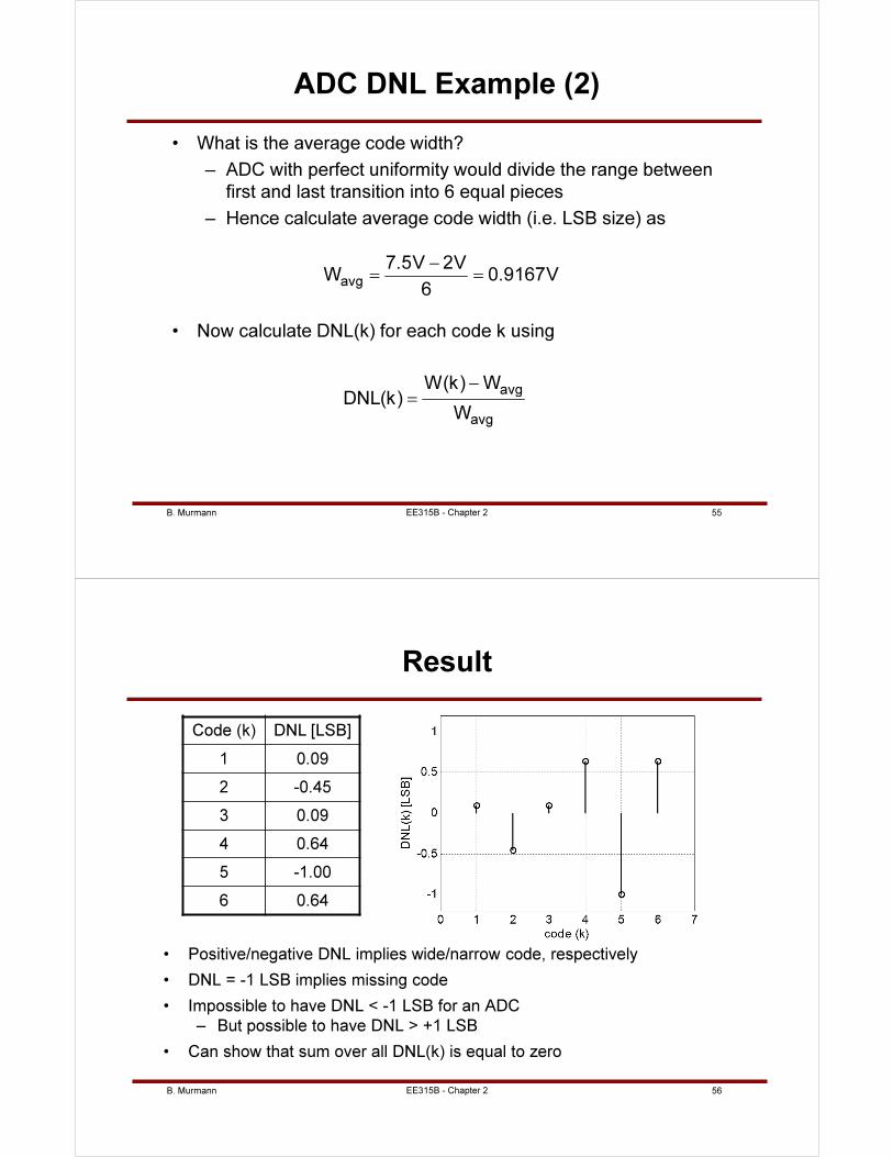
ADC DNL Example (2)
• What is the average code width?
– ADC with perfect uniformity would divide the range between
first and last transition into 6 equal pieces
– Hence calculate average code width (i.e. LSB size) as
avg
7.5V 2VW 0.9167V
6
−
= =
• Now calculate DNL(k) for each code k using
avg
avg
W(k) WDNL(k)
W
−
=
B. Murmann 56EE315B - Chapter 2
Result
• Positive/negative DNL implies wide/narrow code, respectively
• DNL = -1 LSB implies missing code
• Impossible to have DNL < -1 LSB for an ADC
– But possible to have DNL > +1 LSB
• Can show that sum over all DNL(k) is equal to zero
Code (k) DNL [LSB]
1 0.09
2 -0.45
3 0.09
4 0.64
5 -1.00
6 0.64
B. Murmann 57EE315B - Chapter 2
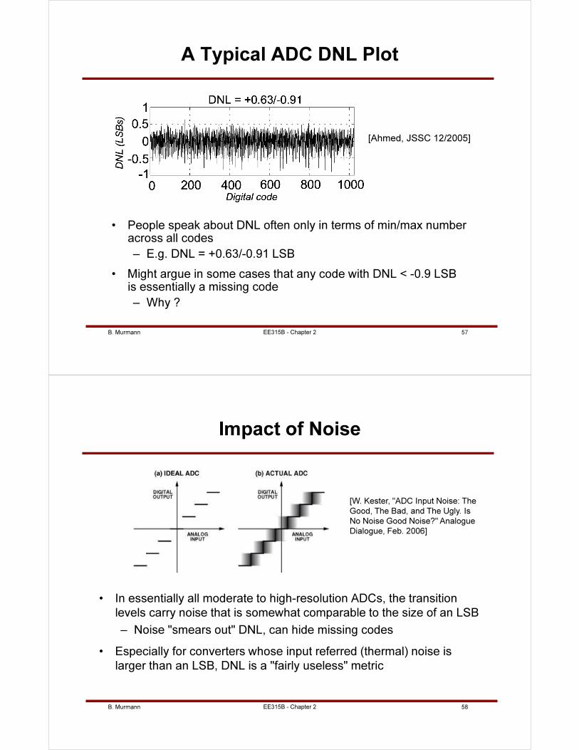
A Typical ADC DNL Plot
• People speak about DNL often only in terms of min/max number across all codes
– E.g. DNL = +0.63/-0.91 LSB
• Might argue in some cases that any code with DNL < -0.9 LSB is essentially a missing code
– Why ?
[Ahmed, JSSC 12/2005]
B. Murmann 58EE315B - Chapter 2
Impact of Noise
• In essentially all moderate to high-resolution ADCs, the transition
levels carry noise that is somewhat comparable to the size of an LSB
– Noise "smears out" DNL, can hide missing codes
• Especially for converters whose input referred (thermal) noise is
larger than an LSB, DNL is a "fairly useless" metric
[W. Kester, "ADC Input Noise: The
Good, The Bad, and The Ugly. Is
No Noise Good Noise?" Analogue
Dialogue, Feb. 2006]
B. Murmann 59EE315B - Chapter 2
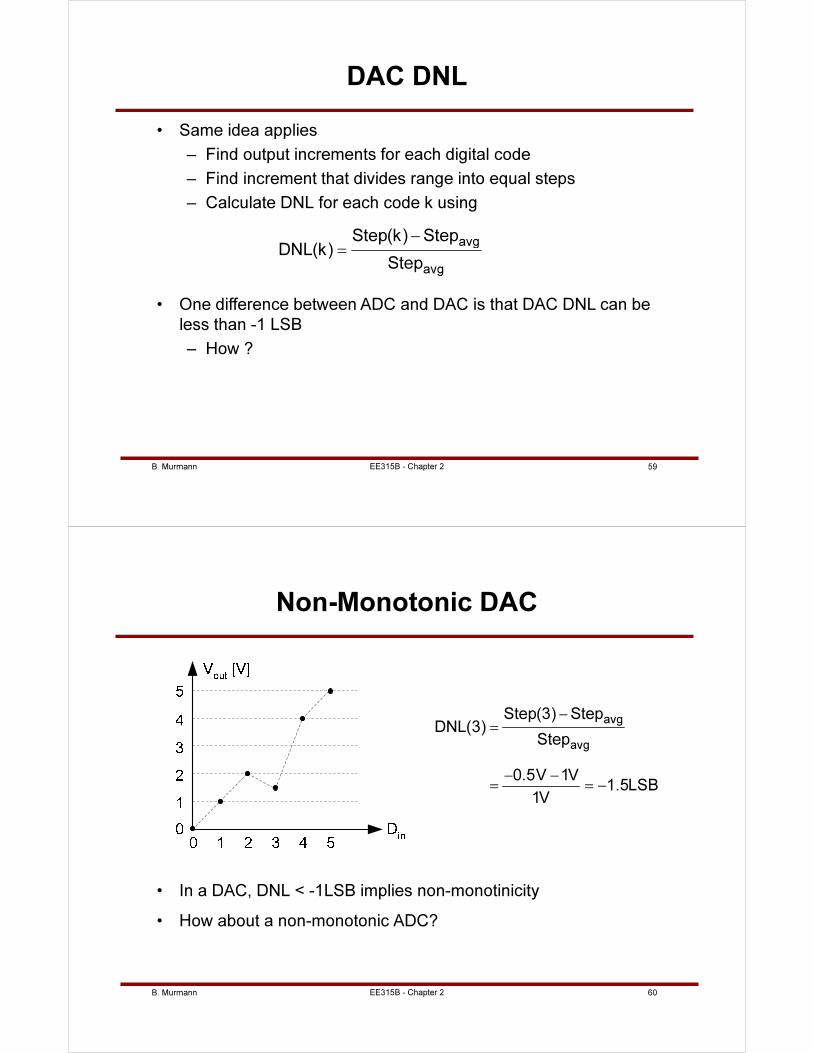
DAC DNL
• Same idea applies
– Find output increments for each digital code
– Find increment that divides range into equal steps
– Calculate DNL for each code k using
avg
avg
Step(k) StepDNL(k)
Step
−
=
• One difference between ADC and DAC is that DAC DNL can be
less than -1 LSB
– How ?
B. Murmann 60EE315B - Chapter 2
Non-Monotonic DAC
• In a DAC, DNL < -1LSB implies non-monotinicity
• How about a non-monotonic ADC?
avg
avg
Step(3) StepDNL(3)
Step
0.5V 1V1.5LSB
1V
−
=
− −
= = −
B. Murmann 61EE315B - Chapter 2
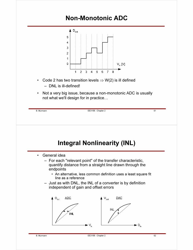
Non-Monotonic ADC
• Code 2 has two transition levels ⇒ W(2) is ill defined
– DNL is ill-defined!
• Not a very big issue, because a non-monotonic ADC is usually
not what we'll design for in practice…
B. Murmann 62EE315B - Chapter 2
Integral Nonlinearity (INL)
• General idea
– For each "relevant point" of the transfer characteristic, quantify distance from a straight line drawn through the endpoints
• An alternative, less common definition uses a least square fit line as a reference
– Just as with DNL, the INL of a converter is by definition independent of gain and offset errors
B. Murmann 63EE315B - Chapter 2
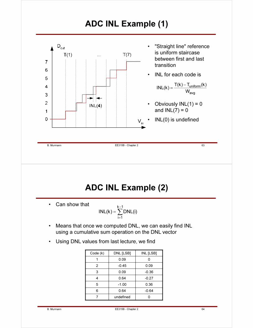
ADC INL Example (1)
• "Straight line" reference
is uniform staircase
between first and last
transition
• INL for each code is
uniform
avg
T(k) T (k)INL(k)
W
−
=
• Obviously INL(1) = 0
and INL(7) = 0
• INL(0) is undefined
B. Murmann 64EE315B - Chapter 2
ADC INL Example (2)
• Can show thatk 1
i 1
INL(k) DNL(i)−
=
=∑
• Means that once we computed DNL, we can easily find INL
using a cumulative sum operation on the DNL vector
• Using DNL values from last lecture, we find
Code (k) DNL [LSB] INL [LSB]
1 0.09 0
2 -0.45 0.09
3 0.09 -0.36
4 0.64 -0.27
5 -1.00 0.36
6 0.64 -0.64
7 undefined 0
B. Murmann 65EE315B - Chapter 2
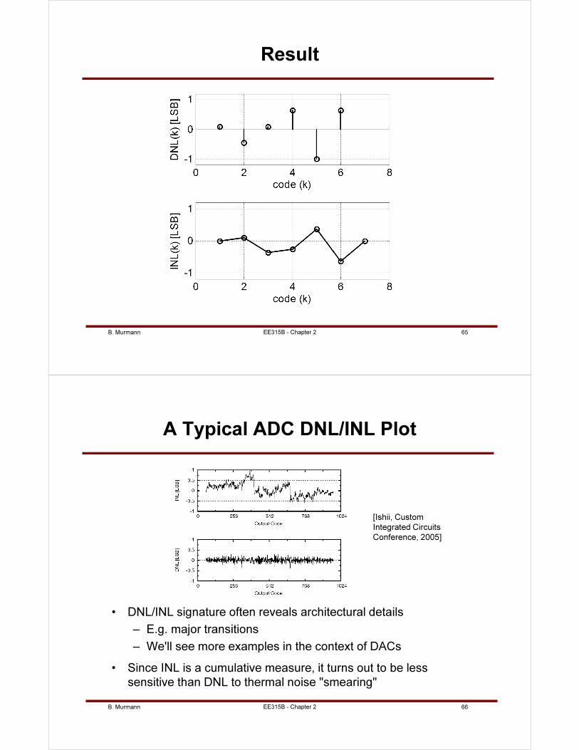
Result
B. Murmann 66EE315B - Chapter 2
A Typical ADC DNL/INL Plot
• DNL/INL signature often reveals architectural details
– E.g. major transitions
– We'll see more examples in the context of DACs
• Since INL is a cumulative measure, it turns out to be less
sensitive than DNL to thermal noise "smearing"
[Ishii, Custom
Integrated Circuits
Conference, 2005]
B. Murmann 67EE315B - Chapter 2
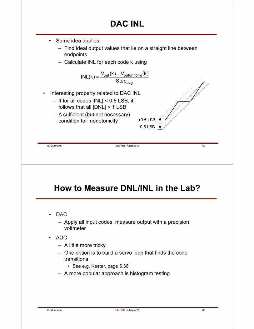
DAC INL
• Same idea applies
– Find ideal output values that lie on a straight line between
endpoints
– Calculate INL for each code k using
out outuniform
avg
V (k) V (k)INL(k)
Step
−
=
• Interesting property related to DAC INL
– If for all codes |INL| < 0.5 LSB, it
follows that all |DNL| < 1 LSB
– A sufficient (but not necessary)
condition for monotonicity
B. Murmann 68
How to Measure DNL/INL in the Lab?
• DAC
– Apply all input codes, measure output with a precision
voltmeter
• ADC
– A little more tricky
– One option is to build a servo loop that finds the code
transitions
• See e.g. Kester, page 5.36
– A more popular approach is histogram testing
EE315B - Chapter 2
B. Murmann 69EE315B - Chapter 2
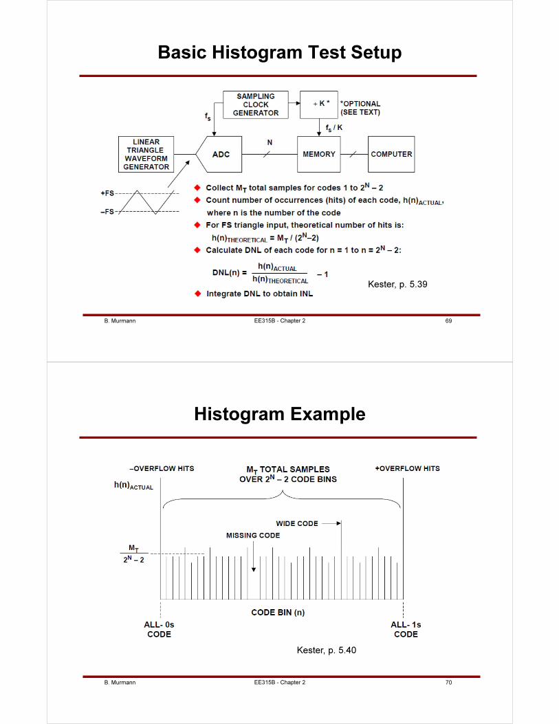
Basic Histogram Test Setup
Kester, p. 5.39
B. Murmann 70
Histogram Example
EE315B - Chapter 2
Kester, p. 5.40
B. Murmann 71
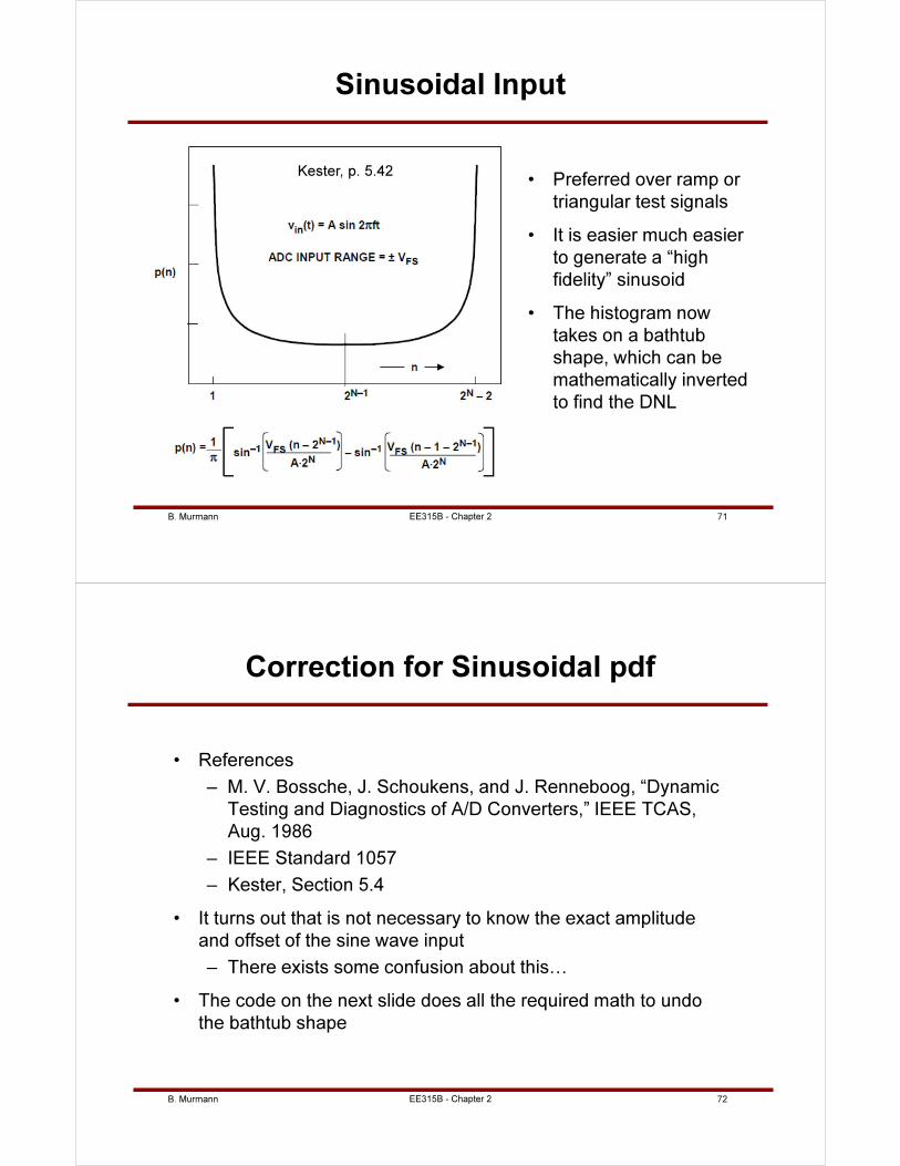
Sinusoidal Input
• Preferred over ramp or
triangular test signals
• It is easier much easier
to generate a “high
fidelity” sinusoid
• The histogram now
takes on a bathtub
shape, which can be
mathematically inverted
to find the DNL
EE315B - Chapter 2
Kester, p. 5.42
B. Murmann 72EE315B - Chapter 2
Correction for Sinusoidal pdf
• References
– M. V. Bossche, J. Schoukens, and J. Renneboog, “Dynamic
Testing and Diagnostics of A/D Converters,” IEEE TCAS,
Aug. 1986
– IEEE Standard 1057
– Kester, Section 5.4
• It turns out that is not necessary to know the exact amplitude
and offset of the sine wave input
– There exists some confusion about this…
• The code on the next slide does all the required math to undo
the bathtub shape
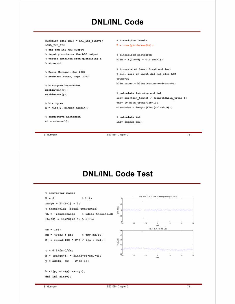
B. Murmann 73EE315B - Chapter 2
DNL/INL Code
function [dnl,inl] = dnl_inl_sin(y);
%DNL_INL_SIN
% dnl and inl ADC output
% input y contains the ADC output
% vector obtained from quantizing a
% sinusoid
% Boris Murmann, Aug 2002
% Bernhard Boser, Sept 2002
% histogram boundaries
minbin=min(y);
maxbin=max(y);
% histogram
h = hist(y, minbin:maxbin);
% cumulative histogram
ch = cumsum(h);
% transition levels
T = -cos(pi*ch/sum(h));
% linearized histogram
hlin = T(2:end) - T(1:end-1);
% truncate at least first and last
% bin, more if input did not clip ADC
trunc=2;
hlin_trunc = hlin(1+trunc:end-trunc);
% calculate lsb size and dnl
lsb= sum(hlin_trunc) / (length(hlin_trunc));
dnl= [0 hlin_trunc/lsb-1];
misscodes = length(find(dnl<-0.9));
% calculate inl
inl= cumsum(dnl);
B. Murmann 74EE315B - Chapter 2
DNL/INL Code Test
% converter model
B = 6; % bits
range = 2^(B-1) - 1;
% thresholds (ideal converter)
th = -range:range; % ideal thresholds
th(20) = th(20)+0.7; % error
fs = 1e6;
fx = 494e3 + pi; % try fs/10!
C = round(100 * 2^B / (fs / fx));
t = 0:1/fs:C/fx;
x = (range+1) * sin(2*pi*fx.*t);
y = adc(x, th) - 2^(B-1);
hist(y, min(y):max(y));
dnl_inl_sin(y);
-30 -20 -10 0 10 20 30-1
-0.5
0
0.5
1
code
DN
L [
LS
B]
DNL = +0.7 / -0.71 LSB, 0 missing codes (DNL<-0.9)
-30 -20 -10 0 10 20 30-0.2
0
0.2
0.4
0.6
0.8
code
INL [
LS
B]
INL = +0.76 / -0.063 LSB
B. Murmann 75EE315B - Chapter 2
Limitations of ADC Histogram Testing
• Cannot detect non-monotonicity
– The histogram does not capture in which order the codes occurred
• Cannot detect erratic dynamics
– E.g. 123, 123, …, 123, 0, 124, 124, …
– Must look directly at ADC output to detect these
• Similarly, random noise is not detected and improves DNL
– E.g. 9, 9, 9, 10, 9, 9, 9, 10, 9, 10, 10, 10, …
• Reference
– B. Ginetti and P. Jespers, “Reliability of Code Density Test for High Resolution ADCs,” Electronics Letters, pp. 2231-2233, Nov. 1991
B. Murmann 76EE315B - Chapter 2
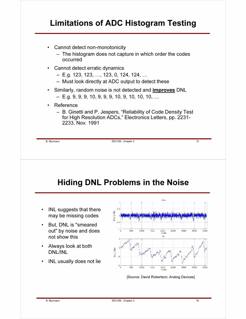
Hiding DNL Problems in the Noise
• INL suggests that there
may be missing codes
• But, DNL is "smeared
out" by noise and does
not show this
• Always look at both
DNL/INL
• INL usually does not lie
[Source: David Robertson, Analog Devices]
B. Murmann 1EE315B - Chapter 3
Spectral Performance Metrics
Boris Murmann
Stanford University
Copyright © 2013 by Boris Murmann
B. Murmann 2EE315B - Chapter 3
Dynamic Performance Metrics
• Time domain
– Glitch impulse, aperture uncertainty, settling time, …
– We'll look at these later, in the context of specific circuits
• Frequency domain
– Performance metrics follow from looking at converter or
building block output spectrum
• "Spectral performance metrics"
– Basic idea: Apply one or more tones at converter input
• Expect same tone(s) at output, all other frequency components
represent nonidealities
– Important to realize that both static (DNL, INL) and dynamic
errors contribute to frequency domain non-ideality
B. Murmann 3EE315B - Chapter 3
Alphabet Soup of Spectral Metrics
• SNR - Signal-to-noise ratio
• SNDR (SINAD) - Signal-to-(noise+distortion) ratio
• ENOB - Effective number of bits
• DR - Dynamic range
• SFDR - Spurious free dynamic range
• HD – Harmonic distortion
• THD - Total harmonic distortion
• ERBW - Effective Resolution Bandwidth
• IMD - Intermodulation distortion
• MTPR - Multi-tone power ratio
B. Murmann 4EE315B - Chapter 3
DAC Tone Test/Simulation Setup
B. Murmann 5EE315B - Chapter 3
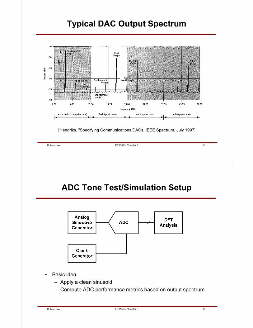
Typical DAC Output Spectrum
[Hendriks, "Specifying Communications DACs, IEEE Spectrum, July 1997]
B. Murmann 6
ADC Tone Test/Simulation Setup
• Basic idea
– Apply a clean sinusoid
– Compute ADC performance metrics based on output spectrum
EE315B - Chapter 3
B. Murmann 7
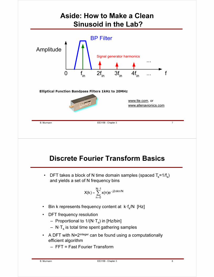
Aside: How to Make a Clean
Sinusoid in the Lab?
EE315B - Chapter 3
0 ... f
Amplitude
BP Filter
fin
...
2fin
3fin
4fin
Signal generator harmonics
www.tte.com, or
www.allenavionics.com
B. Murmann 8EE315B - Chapter 3
Discrete Fourier Transform Basics
• Bin k represents frequency content at k·fs/N [Hz]
• DFT frequency resolution
– Proportional to 1/(N·Ts) in [Hz/bin]
– N·Ts is total time spent gathering samples
• A DFT with N=2integer can be found using a computationally
efficient algorithm
– FFT = Fast Fourier Transform
• DFT takes a block of N time domain samples (spaced Ts=1/fs)
and yields a set of N frequency bins
N 1j2 kn/N
n 0
X(k) x(n)e−
− π
=
= ∑
B. Murmann 9EE315B - Chapter 3
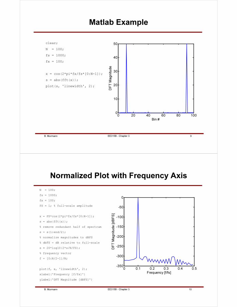
Matlab Example
clear;
N = 100;
fs = 1000;
fx = 100;
x = cos(2*pi*fx/fs*[0:N-1]);
s = abs(fft(x));
plot(s, 'linewidth', 2);
0 20 40 60 80 1000
10
20
30
40
50
Bin #
DF
T M
ag
nitu
de
B. Murmann 10EE315B - Chapter 3
Normalized Plot with Frequency Axis
N = 100;
fs = 1000;
fx = 100;
FS = 1; % full-scale amplitude
x = FS*cos(2*pi*fx/fs*[0:N-1]);
s = abs(fft(x));
% remove redundant half of spectrum
s = s(1:end/2);
% normalize magnitudes to dBFS
% dbFS = dB relative to full-scale
s = 20*log10(2*s/N/FS);
% frequency vector
f = [0:N/2-1]/N;
plot(f, s, 'linewidth', 2);
xlabel('Frequency [f/fs]')
ylabel('DFT Magnitude [dBFS]')
0 0.1 0.2 0.3 0.4 0.5-350
-300
-250
-200
-150
-100
-50
0
Frequency [f/fs]
DF
T M
ag
nitu
de
[d
BF
S]
B. Murmann 11EE315B - Chapter 3
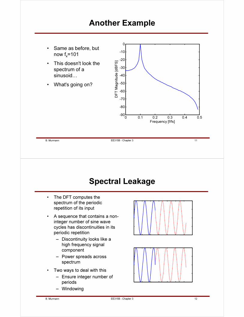
Another Example
0 0.1 0.2 0.3 0.4 0.5-90
-80
-70
-60
-50
-40
-30
-20
-10
0
Frequency [f/fs]
DF
T M
ag
nitu
de
[d
BF
S]
• Same as before, but
now fx=101
• This doesn't look the
spectrum of a
sinusoid…
• What's going on?
B. Murmann 12EE315B - Chapter 3
Spectral Leakage
• The DFT computes the
spectrum of the periodic
repetition of its input
• A sequence that contains a non-
integer number of sine wave
cycles has discontinuities in its
periodic repetition
– Discontinuity looks like a
high frequency signal
component
– Power spreads across
spectrum
• Two ways to deal with this
– Ensure integer number of
periods
– Windowing
B. Murmann 13EE315B - Chapter 3
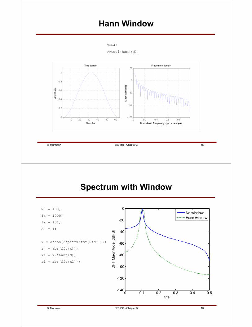
Integer Number of Cycles
N = 100;
cycles = 9;
fs = 1000;
fx = fs*cycles/N;
• Usable test
frequencies are
limited to a multiple
of fs/N
0 0.1 0.2 0.3 0.4 0.5-350
-300
-250
-200
-150
-100
-50
0
Frequency [f/fs]
DF
T M
ag
nitu
de
[d
BF
S]
B. Murmann 14EE315B - Chapter 3
Windowing
• Spectral leakage can be attenuated by windowing the time
samples prior to the DFT
• Windows taper smoothly down to zero at the beginning and the
end of the observation window
• Time domain samples are multiplied by window coefficients on a
sample-by-sample basis
– Means convolution in frequency
– Sine wave tone and other spectral components smear out
over several bins
• Lots of window functions to chose from
– Tradeoff: attenuation versus smearing
• Example: Hann Window
B. Murmann 15EE315B - Chapter 3
Hann Window
10 20 30 40 50 600
0.2
0.4
0.6
0.8
1
Samples
Am
plit
ude
Time domain
0 0.2 0.4 0.6 0.8-150
-100
-50
0
50
Normalized Frequency (×π rad/sample)M
agnitu
de (
dB
)
Frequency domain
N=64;
wvtool(hann(N))
B. Murmann 16EE315B - Chapter 3
Spectrum with Window
N = 100;
fs = 1000;
fx = 101;
A = 1;
x = A*cos(2*pi*fx/fs*[0:N-1]);
s = abs(fft(x));
x1 = x.*hann(N);
s1 = abs(fft(x1));
0 0.1 0.2 0.3 0.4 0.5-140
-120
-100
-80
-60
-40
-20
0
f/fs
DF
T M
ag
nitu
de
[d
BF
S]
No window
Hann window
B. Murmann 17EE315B - Chapter 3
Integer Cycles versus Windowing
• Integer number of cycles
– Test signal falls into single DFT bin
– Requires careful choice of signal frequency
– Ideal for simulations
– In lab measurements, can lock sampling and signal frequency generators (PLL)
• "Coherent sampling"
• Windowing
– No restrictions on signal frequency
– Signal and harmonics distributed over several DFT bins
• Beware of smeared out nonidealities…
– Requires more samples for given accuracy
• More info
– http://www.maxim-ic.com/appnotes.cfm/appnote_number/1040
B. Murmann 18EE315B - Chapter 3
Example
• Now that we've
"calibrated" our test
system, let's look at
some spectra that
involve nonidealities
• First look at
quantization noise
introduced by an
ideal quantizer
N = 2048;
cycles = 67;
fs = 1000;
fx = fs*cycles/N;
LSB = 2/2^10;
%generate signal, quantize (mid-tread) and take FFT
x = cos(2*pi*fx/fs*[0:N-1]);
x = round(x/LSB)*LSB;
s = abs(fft(x));
s = s(1:end/2)/N*2;
% calculate SNR
sigbin = 1 + cycles;
noise = [s(1:sigbin-1), s(sigbin+1:end)];
snr = 10*log10( s(sigbin)^2/sum(noise.^2) );
B. Murmann 19EE315B - Chapter 3
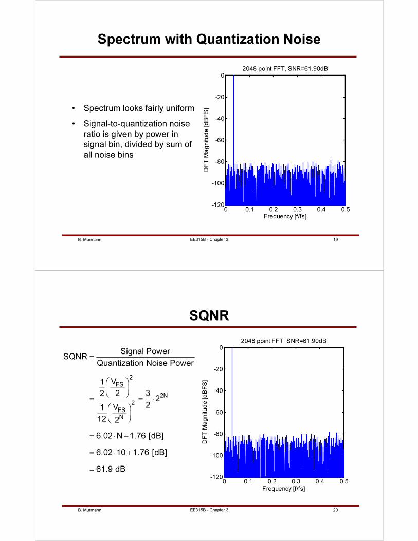
Spectrum with Quantization Noise
• Spectrum looks fairly uniform
• Signal-to-quantization noise
ratio is given by power in
signal bin, divided by sum of
all noise bins
0 0.1 0.2 0.3 0.4 0.5-120
-100
-80
-60
-40
-20
0
Frequency [f/fs]
DF
T M
ag
nitu
de
[d
BF
S]
2048 point FFT, SNR=61.90dB
B. Murmann 20
SQNR
0 0.1 0.2 0.3 0.4 0.5-120
-100
-80
-60
-40
-20
0
Frequency [f/fs]
DF
T M
ag
nitu
de
[d
BF
S]
2048 point FFT, SNR=61.90dB
2
FS
2N
2
FS
N
Signal PowerSQNR
Quantization Noise Power
V1
32 22
2V1
12 2
6.02 N 1.76 [dB]
6.02 10 1.76 [dB]
61.9 dB
=
= = ⋅
= ⋅ +
= ⋅ +
=
EE315B - Chapter 3
B. Murmann 21
0 0.1 0.2 0.3 0.4 0.5-120
-100
-80
-60
-40
-20
0
Frequency [f/fs]
DF
T M
ag
nitu
de
[d
BF
S]
2048 point FFT, SNR=61.90dB
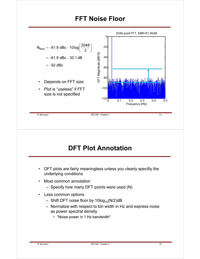
FFT Noise Floor
• Depends on FFT size
• Plot is “useless” if FFT
size is not specified
floor
2048N 61.9 dBc 10log
2
61.9 dBc 30.1 dB
92 dBc
= − −
= − −
= −
EE315B - Chapter 3
B. Murmann 22EE315B - Chapter 3
DFT Plot Annotation
• DFT plots are fairly meaningless unless you clearly specifiy the
underlying conditions
• Most common annotation
– Specify how many DFT points were used (N)
• Less common options
– Shift DFT noise floor by 10log10(N/2)dB
– Normalize with respect to bin width in Hz and express noise
as power spectral density
• "Noise power in 1 Hz bandwidth"
B. Murmann 23EE315B - Chapter 3
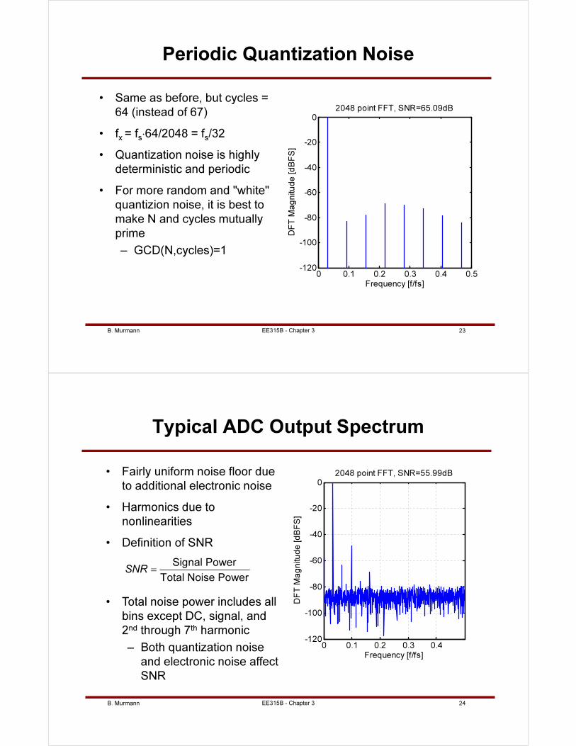
Periodic Quantization Noise
• Same as before, but cycles =
64 (instead of 67)
• fx = fs⋅64/2048 = fs/32
• Quantization noise is highly
deterministic and periodic
• For more random and "white"
quantizion noise, it is best to
make N and cycles mutually
prime
– GCD(N,cycles)=1
0 0.1 0.2 0.3 0.4 0.5-120
-100
-80
-60
-40
-20
0
Frequency [f/fs]D
FT
Ma
gn
itu
de
[d
BF
S]
2048 point FFT, SNR=65.09dB
B. Murmann 24EE315B - Chapter 3
Typical ADC Output Spectrum
• Fairly uniform noise floor due
to additional electronic noise
• Harmonics due to
nonlinearities
• Definition of SNR
Signal Power
Total Noise PowerSNR =
• Total noise power includes all
bins except DC, signal, and
2nd through 7th harmonic
– Both quantization noise
and electronic noise affect
SNR
0 0.1 0.2 0.3 0.4-120
-100
-80
-60
-40
-20
0
Frequency [f/fs]
DF
T M
ag
nitu
de
[d
BF
S]
2048 point FFT, SNR=55.99dB

B. Murmann 25EE315B - Chapter 3
SNDR and ENOB
• Definition
Signal Power
Noise and Distortion PowerSNDR =
• Noise and distortion power
includes all bins except DC
and signal
• Effective number of bits
SNDR(dB)-1.76dB
6.02dBENOB =
0 0.1 0.2 0.3 0.4-120
-100
-80
-60
-40
-20
0
Frequency [f/fs]
DF
T M
ag
nitu
de
[d
BF
S]
2048 point FFT, SNR=55.9dB, SNDR=47.5dB
B. Murmann 26EE315B - Chapter 3
Effective Number of Bits
• Is a 10-Bit converter with 47.5dB SNDR really a 10-bit
converter?
47.5dB 1.76dBENOB 7.6
6.02dB
−
= =
• We get ideal ENOB only for zero electronic noise, perfect
transfer function with zero INL, ...
• Low electronic noise is costly
– Cutting thermal noise down by 2x, can cost 4x in power
dissipation
• Rule of thumb for good power efficiency: ENOB < B-1
– B is the "number of wires" coming out of the ADC or the so
called "stated resolution"
B. Murmann 27EE315B - Chapter 3
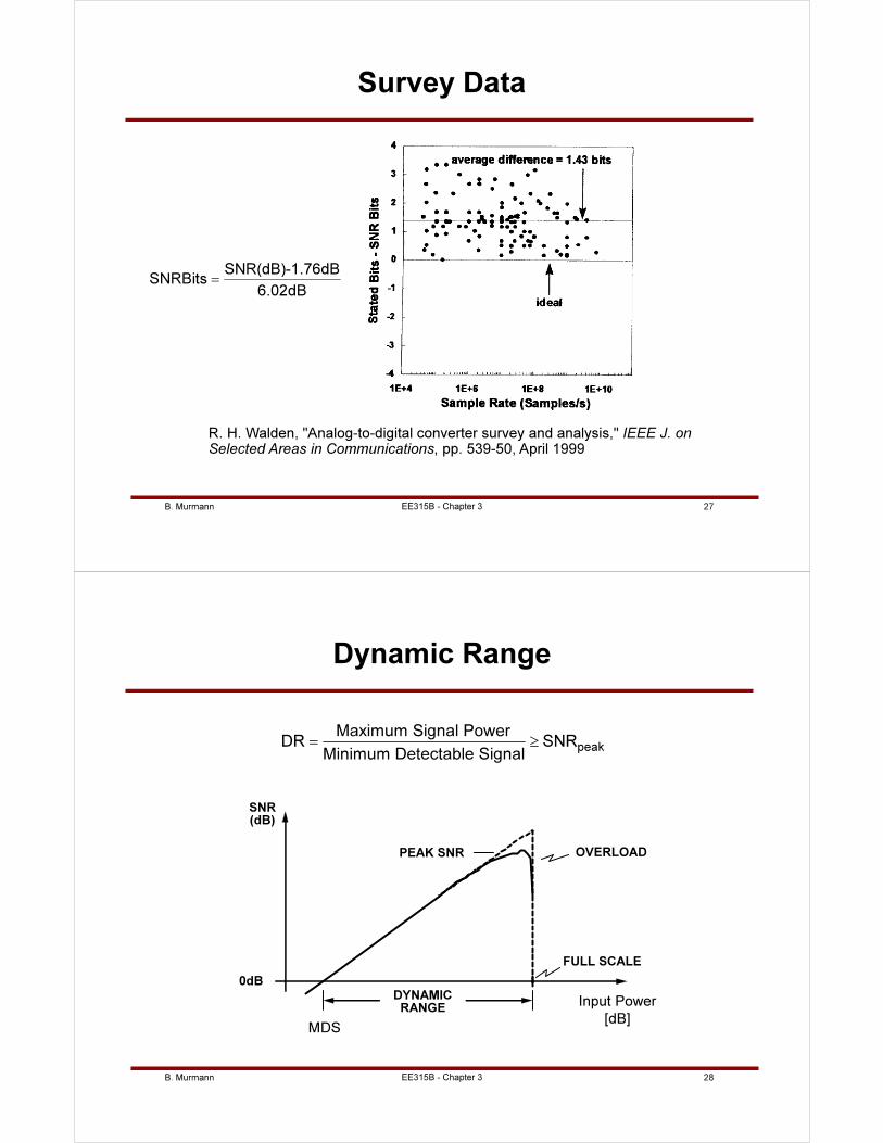
Survey Data
R. H. Walden, "Analog-to-digital converter survey and analysis," IEEE J. on
Selected Areas in Communications, pp. 539-50, April 1999
SNR(dB)-1.76dBSNRBits
6.02dB=
B. Murmann 28
Dynamic Range
peak
Maximum Signal PowerDR SNR
Minimum Detectable Signal= ≥
PEAK SNR OVERLOAD
FULL SCALE
INPUTAMPLITUDE
(dB)
DYNAMICRANGE
0dB
SNR(dB)
Input Power
[dB]MDS
EE315B - Chapter 3
B. Murmann 29EE315B - Chapter 3
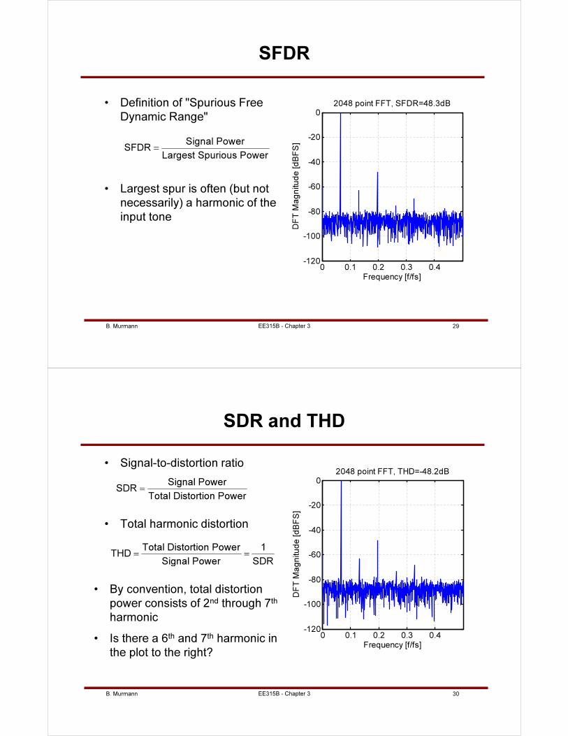
SFDR
• Definition of "Spurious Free
Dynamic Range"
Signal PowerSFDR
Largest Spurious Power=
• Largest spur is often (but not
necessarily) a harmonic of the
input tone
0 0.1 0.2 0.3 0.4-120
-100
-80
-60
-40
-20
0
Frequency [f/fs]
DF
T M
ag
nitu
de
[d
BF
S]
2048 point FFT, SFDR=48.3dB
B. Murmann 30EE315B - Chapter 3
SDR and THD
• Signal-to-distortion ratio
Signal PowerSDR
Total Distortion Power=
• By convention, total distortion
power consists of 2nd through 7th
harmonic
• Is there a 6th and 7th harmonic in
the plot to the right?
0 0.1 0.2 0.3 0.4-120
-100
-80
-60
-40
-20
0
Frequency [f/fs]
DF
T M
ag
nitu
de
[d
BF
S]
2048 point FFT, THD=-48.2dB
Total Distortion Power 1THD
Signal Power SDR= =
• Total harmonic distortion
B. Murmann 31EE315B - Chapter 3
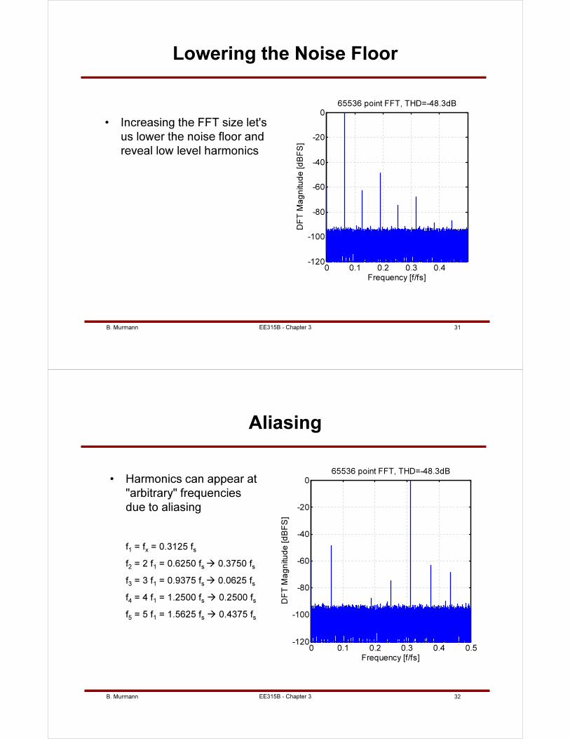
Lowering the Noise Floor
• Increasing the FFT size let's
us lower the noise floor and
reveal low level harmonics
0 0.1 0.2 0.3 0.4-120
-100
-80
-60
-40
-20
0
Frequency [f/fs]
DF
T M
ag
nitu
de
[d
BF
S]
65536 point FFT, THD=-48.3dB
B. Murmann 32EE315B - Chapter 3
Aliasing
• Harmonics can appear at
"arbitrary" frequencies
due to aliasing
f1 = fx = 0.3125 fs
f2 = 2 f1 = 0.6250 fs 0.3750 fs
f3 = 3 f1 = 0.9375 fs 0.0625 fs
f4 = 4 f1 = 1.2500 fs 0.2500 fs
f5 = 5 f1 = 1.5625 fs 0.4375 fs
0 0.1 0.2 0.3 0.4 0.5-120
-100
-80
-60
-40
-20
0
Frequency [f/fs]
DF
T M
ag
nitu
de
[d
BF
S]
65536 point FFT, THD=-48.3dB
B. Murmann 33EE315B - Chapter 3
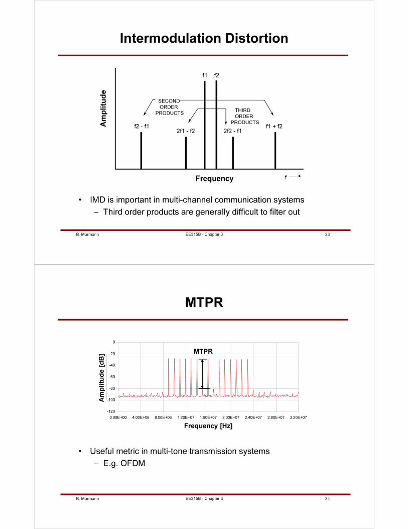
Intermodulation Distortion
• IMD is important in multi-channel communication systems
– Third order products are generally difficult to filter out
Frequency f
f1
f2 - f1
f2
2f1 - f2 2f2 - f1f1 + f2
SECOND
ORDER
PRODUCTSTHIRD
ORDER
PRODUCTSAmplitude
B. Murmann 34EE315B - Chapter 3
MTPR
• Useful metric in multi-tone transmission systems
– E.g. OFDM
-120
-100
-80
-60
-40
-20
0
0.00E+00 4.00E+06 8.00E+06 1.20E+07 1.60E+07 2.00E+07 2.40E+07 2.80E+07 3.20E+07
Frequency(Hz)
MTPR
Frequency [Hz]
Am
pli
tud
e [
dB
]
B. Murmann 35EE315B - Chapter 3
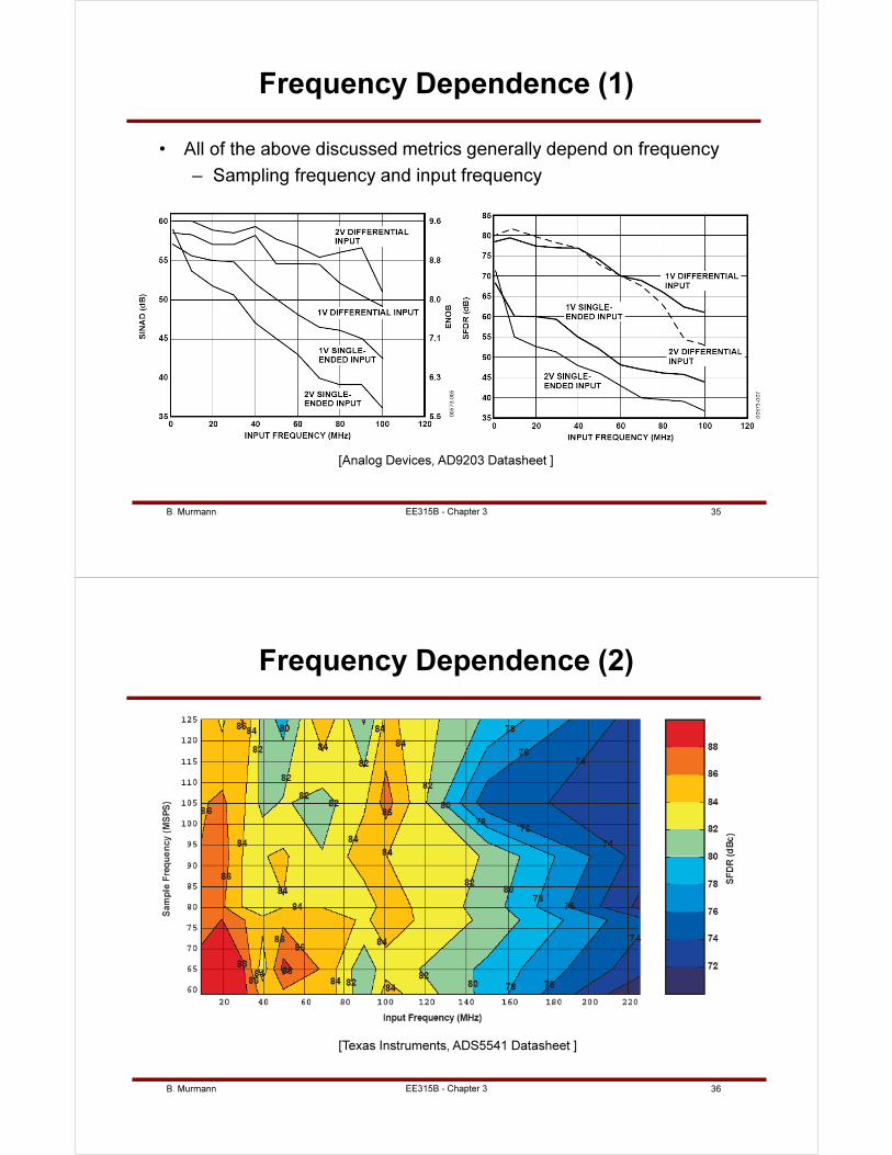
Frequency Dependence (1)
• All of the above discussed metrics generally depend on frequency
– Sampling frequency and input frequency
[Analog Devices, AD9203 Datasheet ]
B. Murmann 36EE315B - Chapter 3
Frequency Dependence (2)
[Texas Instruments, ADS5541 Datasheet ]
B. Murmann 37EE315B - Chapter 3
ERBW
• Defined as the input frequency at which the SNDR of a
converter has dropped by 3dB
– Equivalent to a 0.5-bit loss in ENOB
• ERBW > fs/2 is not uncommon, especially in converters
designed for sub-sampling applications
• ERBW is only a useful metric when the SNDR is relatively flat
initially and gracefully degrades at high frequencies
B. Murmann 38EE315B - Chapter 3
Relationship Between INL and
Harmonic Distortion (1)
• The INL of an ADC often takes on a quadratic or cubic “bow”
– Meaning that the transfer function can be approximated by x+a2x
2 or x+a3x3
• The resulting harmonic distortion usually sets the low frequency SFDR
Input
Output
Ideal
Quadratic bow
Cubic bow
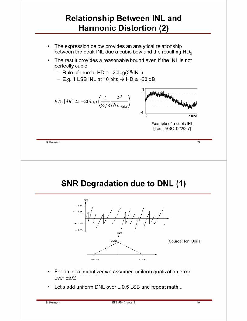
B. Murmann 39
Relationship Between INL and
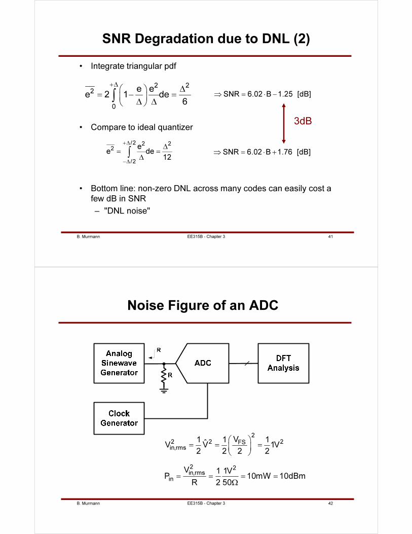
Harmonic Distortion (2)
• The expression below provides an analytical relationship between the peak INL due a cubic bow and the resulting HD3
• The result provides a reasonable bound even if the INL is not perfectly cubic
– Rule of thumb: HD ≅ -20log(2B/INL)
– E.g. 1 LSB INL at 10 bits HD ≅ -60 dB
Example of a cubic INL
[Lee, JSSC 12/2007]
≅ 204
3 3
2
B. Murmann 40EE315B - Chapter 3
SNR Degradation due to DNL (1)
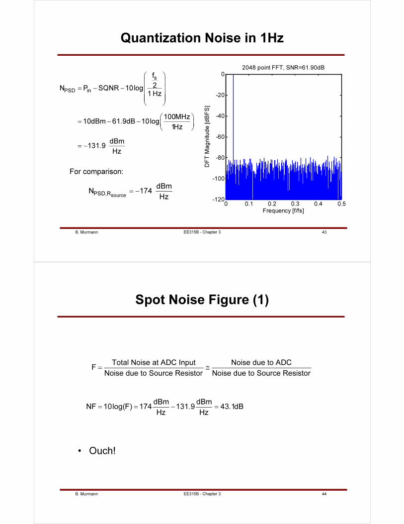
• For an ideal quantizer we assumed uniform quatization error
over ±∆/2
• Let's add uniform DNL over ± 0.5 LSB and repeat math...
[Source: Ion Opris]
B. Murmann 41EE315B - Chapter 3
SNR Degradation due to DNL (2)
• Integrate triangular pdf
• Compare to ideal quantizer
• Bottom line: non-zero DNL across many codes can easily cost a
few dB in SNR
– "DNL noise"
2 22
0
e ee 2 1 de
6
+∆∆
= − = ∆ ∆ ∫
/2 2 22
/2
ee de
12
+∆
−∆
∆= =
∆∫
SNR 6.02 B 1.25 [dB]⇒ = ⋅ −
SNR 6.02 B 1.76 [dB]⇒ = ⋅ +
3dB
B. Murmann 42
Noise Figure of an ADC
22 2 2FSin,rms
2 2in,rms
in
V1 1 1ˆV V 1V
2 2 2 2
V 1 1VP 10mW 10dBm
R 2 50
= = =
= = = =Ω
EE315B - Chapter 3
B. Murmann 43
Quantization Noise in 1Hz
s
PSD in
f
2N P SQNR 10log1 Hz
100MHz10dBm 61.9dB 10log
1Hz
dBm131.9
Hz
= − −
= − −
= −
sourcePSD,R
dBmN 174
Hz= −
For comparison:
0 0.1 0.2 0.3 0.4 0.5-120
-100
-80
-60
-40
-20
0
Frequency [f/fs]D
FT
Ma
gn
itu
de
[d
BF
S]
2048 point FFT, SNR=61.90dB
EE315B - Chapter 3
B. Murmann 44
Spot Noise Figure (1)
Total Noise at ADC Input Noise due to ADCF
Noise due to Source Resistor Noise due to Source Resistor
dBm dBmNF 10log(F) 174 131.9 43.1dB
Hz Hz
= ≅
= = − =
• Ouch!
EE315B - Chapter 3
B. Murmann 45
Spot Noise Figure (2)
• Improve NF by increasing R (need a transformer),
resolution (N) and fs
s
in
2
FS s
2N
fdBm 2NF 174 P SQNR 10logHz 1 Hz
V1 fdBm 32 2 2174 10log 10log 2 10logHz R 2 1 Hz
= + − −
= + − −
EE315B - Chapter 3
B. Murmann 46
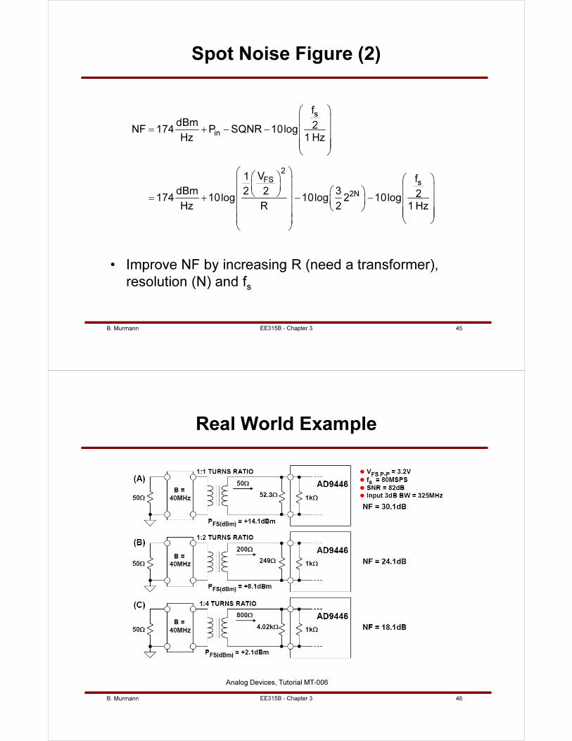
Real World Example
Analog Devices, Tutorial MT-006
EE315B - Chapter 3
B. Murmann 1EE315B - Chapter 4
Nyquist Rate DACs
Boris Murmann
Stanford University
Copyright © 2013 by Boris Murmann
B. Murmann 2EE315B - Chapter 4
Overview
• D/A conversion is typically accomplished through the division or
multiplication of a reference voltage, current or charge
• Basic configurations
– Thermometer
– Binary weighted
– Segmented
• Implementation choices
– Resistive, capacitive, current steering
– Nyquist rate, oversampling, PWM
– …
• Our discussion will focus mainly on high-speed current steering
B. Murmann 3EE315B - Chapter 4
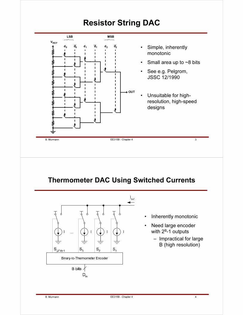
Resistor String DAC
• Simple, inherently
monotonic
• Small area up to ~8 bits
• See e.g. Pelgrom,
JSSC 12/1990
• Unsuitable for high-
resolution, high-speed
designs
OUT
VREF
d0 d0 d1 d1 d2 d2
xxxxx
LSB
xxxxx
MSB
B. Murmann 4EE315B - Chapter 4
Thermometer DAC Using Switched Currents
• Inherently monotonic
• Need large encoder
with 2B-1 outputs
– Impractical for large
B (high resolution)
B. Murmann 5
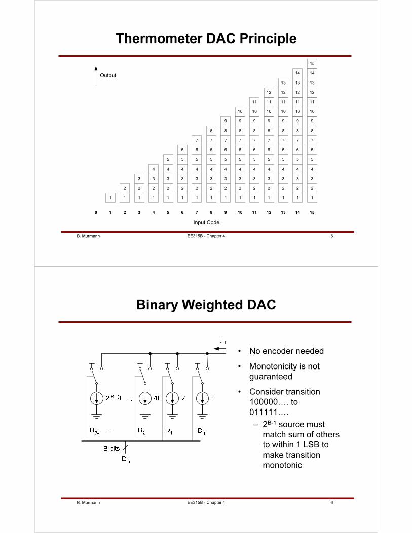
Thermometer DAC Principle
1 1
2
1
2
1
2
1
2
1
2
3 3
4
3
4
5
3
4
5
6
1
2
1
2
1
2
1
2
3
4
5
6
7
3
4
5
6
7
8
3
4
5
6
7
8
9
3
4
5
6
7
8
9
10
1
2
1
2
1
2
1
2
3
4
5
6
7
8
9
10
11
3
4
5
6
7
8
9
10
11
12
3
4
5
6
7
8
9
10
11
12
13
3
4
5
6
7
8
9
10
11
12
13
14
1
2
3
4
5
6
7
8
9
10
11
12
13
14
15
1 2 3 4 5 6 7 8 9 10 11 12 13 14 150
Output
Input Code
EE315B - Chapter 4
B. Murmann 6EE315B - Chapter 4
Binary Weighted DAC
• No encoder needed
• Monotonicity is not
guaranteed
• Consider transition
100000…. to
011111….
– 2B-1 source must
match sum of others
to within 1 LSB to
make transition
monotonic
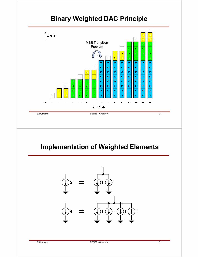
B. Murmann 7
Binary Weighted DAC Principle
MSB Transition
Problem
EE315B - Chapter 4
B. Murmann 8EE315B - Chapter 4
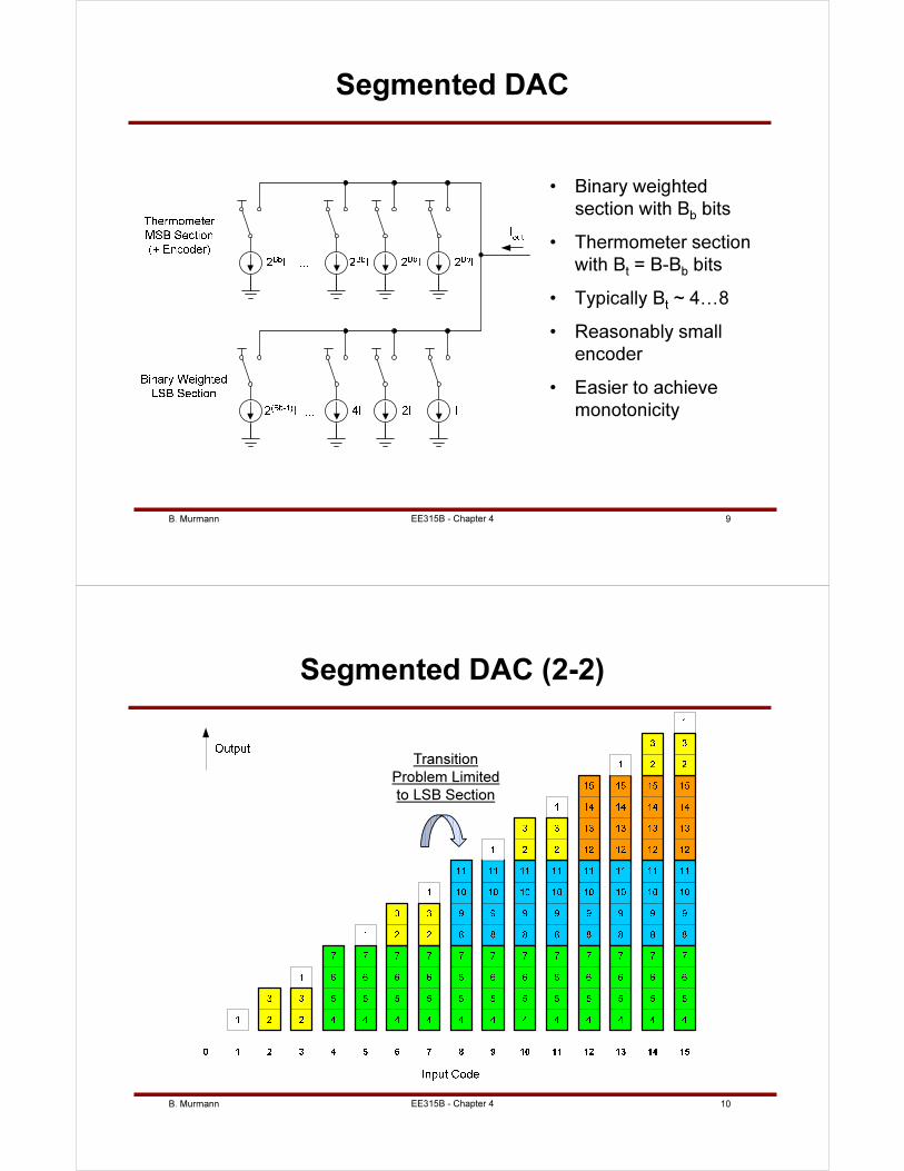
Implementation of Weighted Elements
B. Murmann 9EE315B - Chapter 4
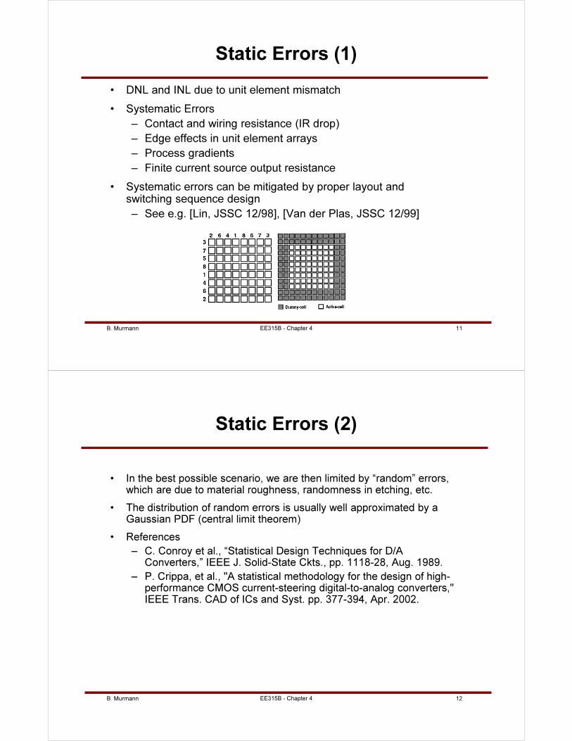
Segmented DAC
• Binary weighted
section with Bb bits
• Thermometer section
with Bt = B-Bb bits
• Typically Bt ~ 4…8
• Reasonably small
encoder
• Easier to achieve
monotonicity
B. Murmann 10
Segmented DAC (2-2)
Transition
Problem Limited
to LSB Section
EE315B - Chapter 4
B. Murmann 11
Static Errors (1)
• DNL and INL due to unit element mismatch
• Systematic Errors
– Contact and wiring resistance (IR drop)
– Edge effects in unit element arrays
– Process gradients
– Finite current source output resistance
• Systematic errors can be mitigated by proper layout and switching sequence design
– See e.g. [Lin, JSSC 12/98], [Van der Plas, JSSC 12/99]
EE315B - Chapter 4
B. Murmann 12EE315B - Chapter 4
Static Errors (2)
• In the best possible scenario, we are then limited by “random” errors, which are due to material roughness, randomness in etching, etc.
• The distribution of random errors is usually well approximated by a Gaussian PDF (central limit theorem)
• References
– C. Conroy et al., “Statistical Design Techniques for D/A Converters,” IEEE J. Solid-State Ckts., pp. 1118-28, Aug. 1989.
– P. Crippa, et al., "A statistical methodology for the design of high-performance CMOS current-steering digital-to-analog converters," IEEE Trans. CAD of ICs and Syst. pp. 377-394, Apr. 2002.
B. Murmann 13EE315B - Chapter 4
Gaussian Distribution
( )2
2
x
21
f(x) e2
−µ−
σ=
πσ
-3 -2 -1 0 1 2 30
0.1
0.2
0.3
0.4
x/σ
f(x)
xX
− µ=
σ
X
B. Murmann 14EE315B - Chapter 4
Yield (1)
( )
2XC
2
C
1 CP C X C e dX erf
2 2
+−
−
− ≤ ≤ + = =
π ∫
0 0.5 1 1.5 2 2.5 30
0.2
0.4
0.6
0.8
1
X/σ
P(-
X ≤
x ≤
+X
)
C
P(-
C ≤
X ≤
C)
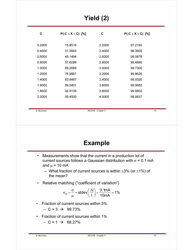
B. Murmann 15EE315B - Chapter 4
Yield (2)
C P(-C ≤ X ≤ C) [%]
0.2000 15.8519
0.4000 31.0843
0.6000 45.1494
0.8000 57.6289
1.0000 68.2689
1.2000 76.9861
1.4000 83.8487
1.6000 89.0401
1.8000 92.8139
2.0000 95.4500
C P(-C ≤ X ≤ C) [%]
2.2000 97.2193
2.4000 98.3605
2.6000 99.0678
2.8000 99.4890
3.0000 99.7300
3.2000 99.8626
3.4000 99.9326
3.6000 99.9682
3.8000 99.9855
4.0000 99.9937
B. Murmann 16EE315B - Chapter 4
Example
• Measurements show that the current in a production lot of
current sources follows a Gaussian distribution with σ = 0.1 mA
and µ = 10 mA
– What fraction of current sources is within ±3% (or ±1%) of
the mean?
• Relative matching ("coefficient of variation")
u
I 0.1mAstdev 1%
I 10mA
σ ∆ σ = = = = µ
• Fraction of current sources within 3%
– C = 3 99.73%
• Fraction of current sources within 1%
– C = 1 68.27%
B. Murmann 17EE315B - Chapter 4
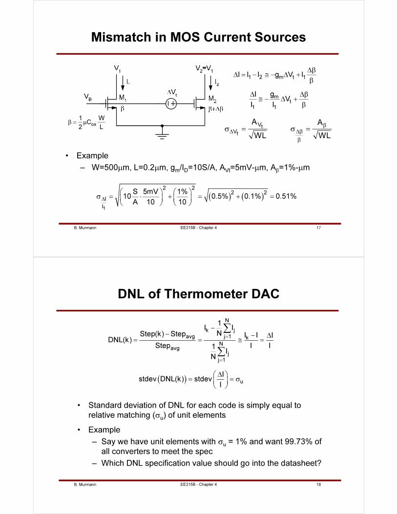
Mismatch in MOS Current Sources
1 2 m t 1I I I g V I
∆β∆ = − ≅ − ∆ +
β
mt
1 1
gIV
I I
∆ ∆β≅ − ∆ +
β
( ) ( )1
2 22 2
I
I
S 5mV 1%10 0.5% 0.1% 0.51%
A 10 10∆
σ = ⋅ + = + =
• Example
– W=500µm, L=0.2µm, gm/ID=10S/A, AVt=5mV-µm, Aβ=1%-µm
t
t
V
V
A A
WL WL
β∆ ∆β
β
σ = σ =
ox
1 WC
2 Lβ = µ
B. Murmann 18EE315B - Chapter 4
DNL of Thermometer DAC
• Standard deviation of DNL for each code is simply equal to
relative matching (σu) of unit elements
• Example
– Say we have unit elements with σu = 1% and want 99.73% of
all converters to meet the spec
– Which DNL specification value should go into the datasheet?
( )
N
k javg j 1 k
Navg
jj 1
u
1I I
NStep(k) Step I I IDNL(k)
Step I I1I
N
Istdev DNL(k) stdev
I
=
=
−− − ∆
= = ≅ =
∆ = = σ
∑
∑
B. Murmann 19EE315B - Chapter 4
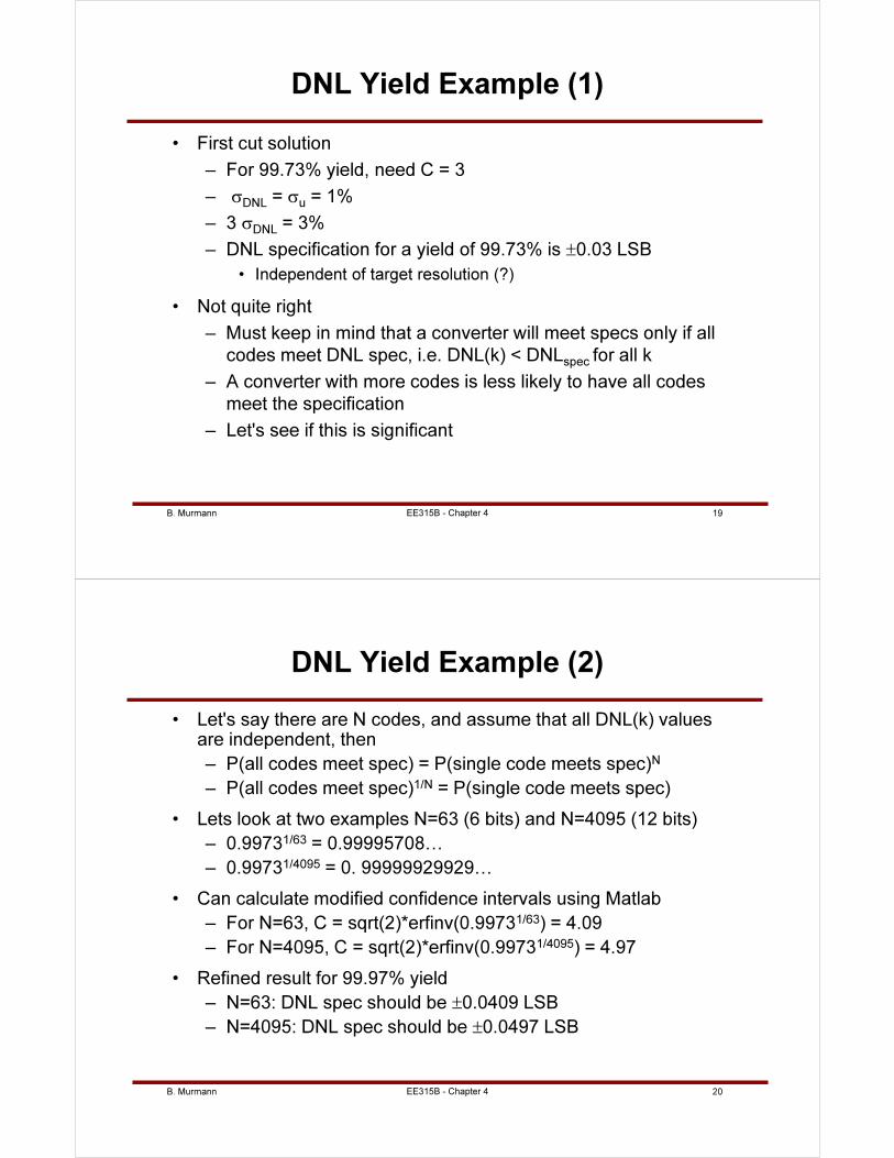
DNL Yield Example (1)
• First cut solution
– For 99.73% yield, need C = 3
– σDNL = σu = 1%
– 3 σDNL = 3%
– DNL specification for a yield of 99.73% is ±0.03 LSB
• Independent of target resolution (?)
• Not quite right
– Must keep in mind that a converter will meet specs only if all
codes meet DNL spec, i.e. DNL(k) < DNLspec for all k
– A converter with more codes is less likely to have all codes
meet the specification
– Let's see if this is significant
B. Murmann 20EE315B - Chapter 4
DNL Yield Example (2)
• Let's say there are N codes, and assume that all DNL(k) values are independent, then
– P(all codes meet spec) = P(single code meets spec)N
– P(all codes meet spec)1/N = P(single code meets spec)
• Lets look at two examples N=63 (6 bits) and N=4095 (12 bits)
– 0.99731/63 = 0.99995708…
– 0.99731/4095 = 0. 99999929929…
• Can calculate modified confidence intervals using Matlab
– For N=63, C = sqrt(2)*erfinv(0.99731/63) = 4.09
– For N=4095, C = sqrt(2)*erfinv(0.99731/4095) = 4.97
• Refined result for 99.97% yield
– N=63: DNL spec should be ±0.0409 LSB
– N=4095: DNL spec should be ±0.0497 LSB
B. Murmann 21EE315B - Chapter 4
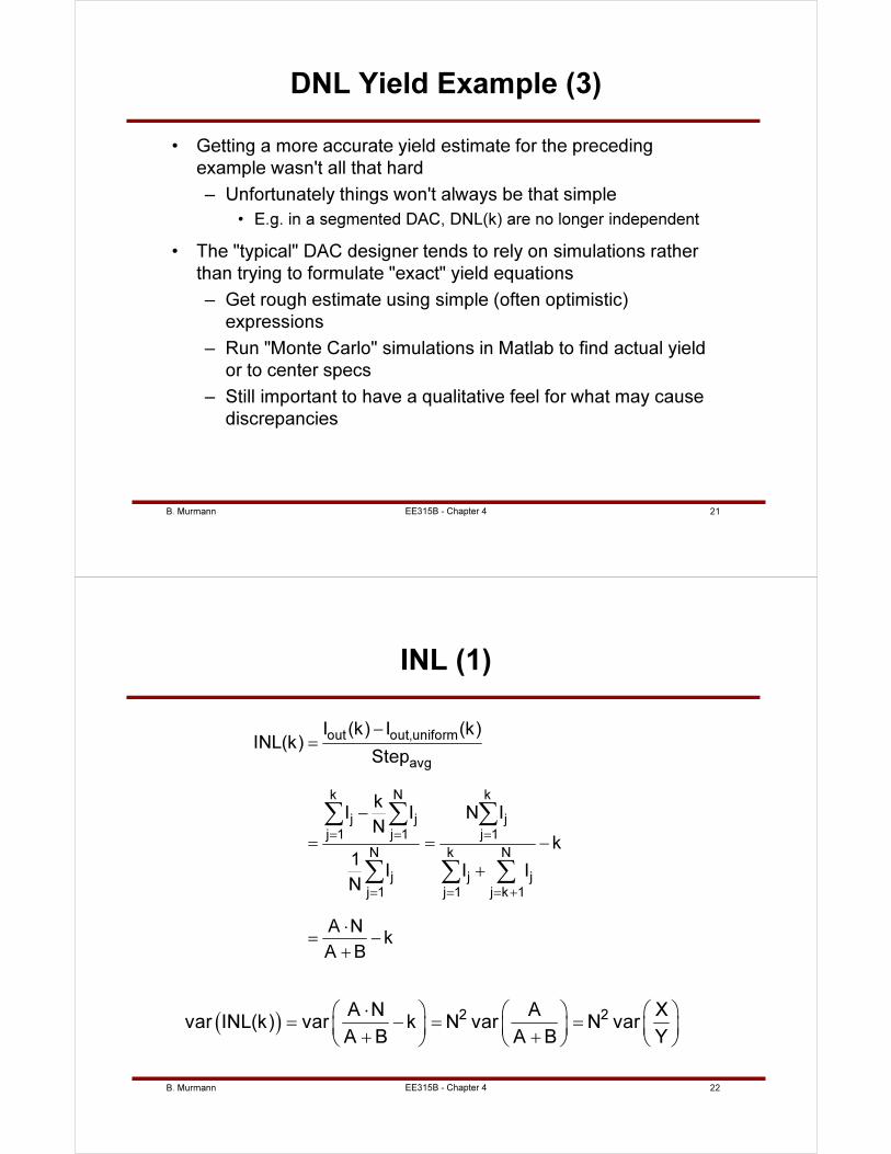
DNL Yield Example (3)
• Getting a more accurate yield estimate for the preceding
example wasn't all that hard
– Unfortunately things won't always be that simple
• E.g. in a segmented DAC, DNL(k) are no longer independent
• The "typical" DAC designer tends to rely on simulations rather
than trying to formulate "exact" yield equations
– Get rough estimate using simple (often optimistic)
expressions
– Run "Monte Carlo" simulations in Matlab to find actual yield
or to center specs
– Still important to have a qualitative feel for what may cause
discrepancies
B. Murmann 22EE315B - Chapter 4
INL (1)
out out,uniform
avg
k N k
j j jj 1 j 1 j 1
N k N
j j jj 1 j 1 j k 1
I (k) I (k)INL(k)
Step
kI I N I
Nk
1I I I
N
A Nk
A B
= = =
= = = +
−
=
−
= = −
+
⋅= −
+
∑ ∑ ∑
∑ ∑ ∑
( ) 2 2A N A Xvar INL(k) var k N var N var
A B A B Y
⋅ = − = = + +
B. Murmann 23EE315B - Chapter 4
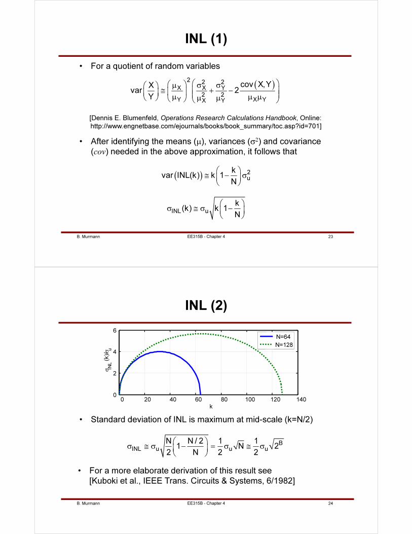
INL (1)
• For a quotient of random variables
( )2 2 2
X X Y
2 2Y X YX Y
cov X,YXvar 2
Y
µ σ σ ≅ + − µ µ µµ µ
[Dennis E. Blumenfeld, Operations Research Calculations Handbook, Online:
http://www.engnetbase.com/ejournals/books/book_summary/toc.asp?id=701]
• After identifying the means (µ), variances (σ2) and covariance
(cov) needed in the above approximation, it follows that
( ) 2
u
kvar INL(k) k 1
N
≅ − σ
INL u
k(k) k 1
N
σ ≅ σ −
B. Murmann 24EE315B - Chapter 4
INL (2)
• Standard deviation of INL is maximum at mid-scale (k=N/2)
B
INL u u u
N N / 2 1 11 N 2
2 N 2 2
σ ≅ σ − = σ ≅ σ
• For a more elaborate derivation of this result see
[Kuboki et al., IEEE Trans. Circuits & Systems, 6/1982]
0 20 40 60 80 100 120 1400
2
4
6
k
σIN
L(k)/σu
N=64
N=128
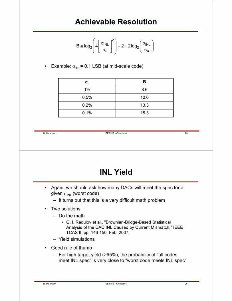
B. Murmann 25EE315B - Chapter 4
Achievable Resolution
• Example: σINL= 0.1 LSB (at mid-scale code)
2
INL INL2 2
u u
B log 4 2 2log σ σ ≅ = + σ σ
σu
B
1% 8.6
0.5% 10.6
0.2% 13.3
0.1% 15.3
B. Murmann 26EE315B - Chapter 4
INL Yield
• Again, we should ask how many DACs will meet the spec for a
given σINL (worst code)
– It turns out that this is a very difficult math problem
• Two solutions
– Do the math
• G. I. Radulov et al., "Brownian-Bridge-Based Statistical
Analysis of the DAC INL Caused by Current Mismatch," IEEE
TCAS II, pp. 146-150, Feb. 2007.
– Yield simulations
• Good rule of thumb
– For high target yield (>95%), the probability of "all codes
meet INL spec" is very close to "worst code meets INL spec"
B. Murmann 27EE315B - Chapter 4
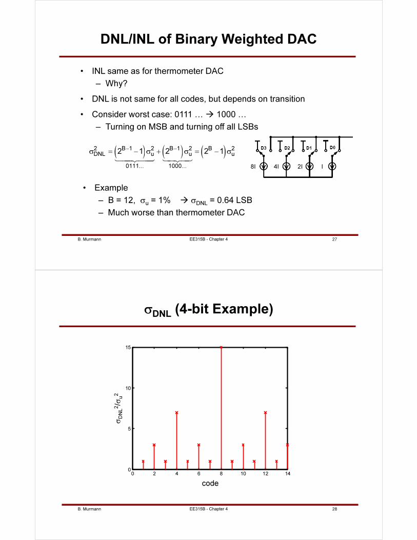
DNL/INL of Binary Weighted DAC
• INL same as for thermometer DAC
– Why?
• DNL is not same for all codes, but depends on transition
• Consider worst case: 0111 … 1000 …
– Turning on MSB and turning off all LSBs
( ) ( ) ( )2 B 1 2 B 1 2 B 2
DNL u u u
0111... 1000...
2 1 2 2 1− −
σ = − σ + σ = − σ
1442443 14243
• Example
– B = 12, σu = 1% σDNL = 0.64 LSB
– Much worse than thermometer DAC
I2I4I8I
B. Murmann 28EE315B - Chapter 4
σDNL
(4-bit Example)
0 2 4 6 8 10 12 140
5
10
15
DAC input code
( σDNL /
σε )2
code
σDNL2/σ
u2
B. Murmann 29EE315B - Chapter 4
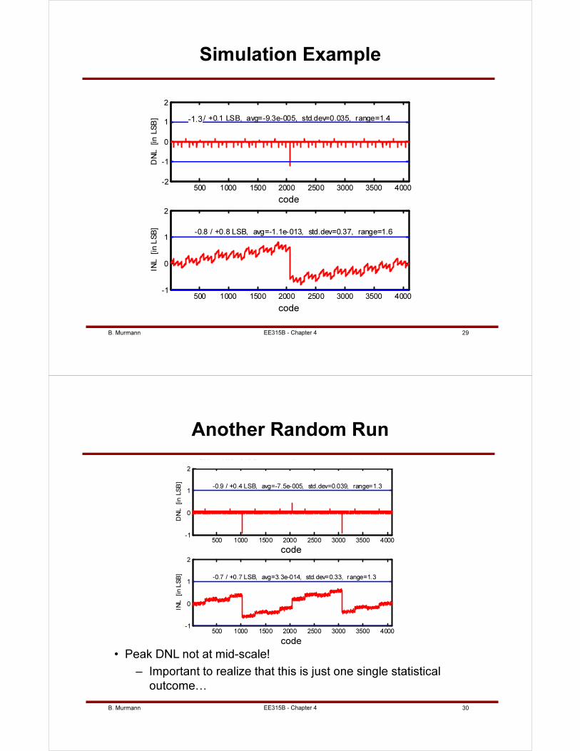
Simulation Example
500 1000 1500 2000 2500 3000 3500 4000-2
-1
0
1
2
bin
DN
L
[in L
SB
]
DNL and INL of 12 Bit converter (from converter decision thresholds)
-1 / +0.1 LSB, avg=-9.3e-005, std.dev=0.035, range=1.4
500 1000 1500 2000 2500 3000 3500 4000-1
0
1
2
bin
INL
[in L
SB
]
-0.8 / +0.8 LSB, avg=-1.1e-013, std.dev=0.37, range=1.6
code
code
-1.3
B. Murmann 30EE315B - Chapter 4
Another Random Run
• Peak DNL not at mid-scale!
– Important to realize that this is just one single statistical
outcome…
500 1000 1500 2000 2500 3000 3500 4000-1
0
1
2
bin
DN
L
[in L
SB
]
DNL and INL of 12 Bit converter (from converter decision thresholds)
-0.9 / +0.4 LSB, avg=-7.5e-005, std.dev=0.039, range=1.3
500 1000 1500 2000 2500 3000 3500 4000-1
0
1
2
bin
INL
[in L
SB
]
-0.7 / +0.7 LSB, avg=3.3e-014, std.dev=0.33, range=1.3
code
code
B. Murmann 31EE315B - Chapter 4
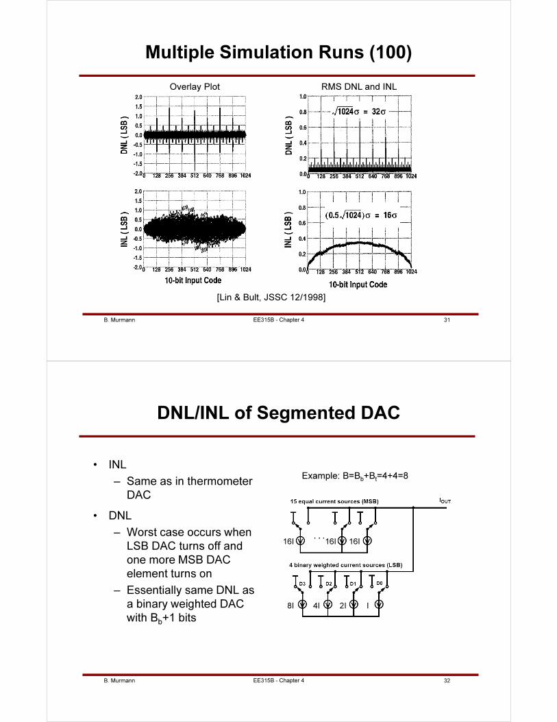
Multiple Simulation Runs (100)
Overlay Plot RMS DNL and INL
[Lin & Bult, JSSC 12/1998]
B. Murmann 32EE315B - Chapter 4
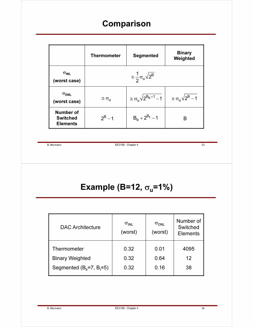
DNL/INL of Segmented DAC
• INL
– Same as in thermometer
DAC
• DNL
– Worst case occurs when
LSB DAC turns off and
one more MSB DAC
element turns on
– Essentially same DNL as
a binary weighted DAC
with Bb+1 bitsI2I4I8I
16I 16I 16I
Example: B=Bb+Bt=4+4=8
B. Murmann 33EE315B - Chapter 4
Comparison
Thermometer SegmentedBinary
Weighted
σINL
(worst case)
σDNL
(worst case)
Number of
Switched
Elements
B
u
12
2≅ σ
bB 1
u 2 1+
≅ σ −u≅ σ
B
u2 1≅ σ −
B2 1−
tB
bB 2 1+ − B
B. Murmann 34EE315B - Chapter 4
Example (B=12, σu=1%)
DAC ArchitectureσINL
(worst)
σDNL
(worst)
Number of
Switched
Elements
Thermometer
Binary Weighted
Segmented (Bb=7, Bt=5)
0.32
0.32
0.32
0.01
0.64
0.16
4095
12
38
B. Murmann 35EE315B - Chapter 4
Dynamic DAC Errors (1)
• Finite settling time and slewing
– Finite RC time constant
– Signal dependent slewing
• Feedthrough
– Coupling from switch signals to DAC output
– Clock feedthrough
• Glitches due to timing errors
– Current sources won’t switch simultaneously
• Dynamic DAC errors are generally hard to model!
B. Murmann 36EE315B - Chapter 4
Dynamic DAC Errors (2)
• References
– Gustavsson, Chapter 12
– M. Albiol, J.L. Gonzalez, E. Alarcon, "Mismatch and dynamic
modeling of current sources in current-steering CMOS D/A
converters," IEEE TCAS I, pp. 159-169, Jan. 2004
– Doris, van Roermund, Leenaerts, Wide-Bandwidth High
Dynamic Range D/A Converters, Springer 2006.
– T. Chen and G.G.E. Gielen, "The analysis and improvement
of a current-steering DAC's dynamic SFDR," IEEE Trans.
Ckts. Syst. I, pp. 3-15, Jan. 2006.
B. Murmann 37EE315B - Chapter 4
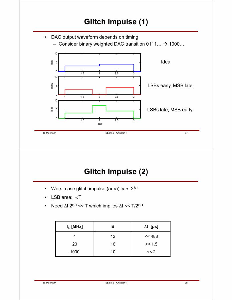
Glitch Impulse (1)
• DAC output waveform depends on timing
– Consider binary weighted DAC transition 0111… 1000…
1 1.5 2 2.5 30
5
10ideal
1 1.5 2 2.5 30
5
10
early
1 1.5 2 2.5 30
5
10
Time
late
Ideal
LSBs early, MSB late
LSBs late, MSB early
B. Murmann 38EE315B - Chapter 4
Glitch Impulse (2)
• Worst case glitch impulse (area): ∝∆t 2B-1
• LSB area: ∝T
• Need ∆t 2B-1 << T which implies ∆t << T/2B-1
fs
[MHz] B ∆t [ps]
1
20
1000
12
16
10
<< 488
<< 1.5
<< 2
B. Murmann 39EE315B - Chapter 4
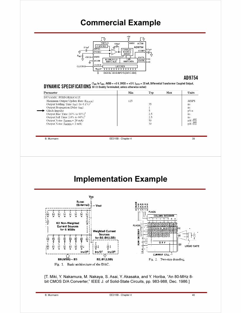
Commercial Example
B. Murmann 40EE315B - Chapter 4
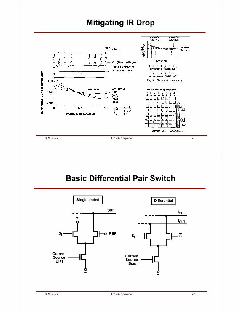
Implementation Example
[T. Miki, Y. Nakamura, M. Nakaya, S. Asai, Y. Akasaka, and Y. Horiba, “An 80-MHz 8-
bit CMOS D/A Converter,” IEEE J. of Solid-State Circuits, pp. 983-988, Dec. 1986.]
B. Murmann 41EE315B - Chapter 4
Mitigating IR Drop
B. Murmann 42EE315B - Chapter 4
Basic Differential Pair Switch
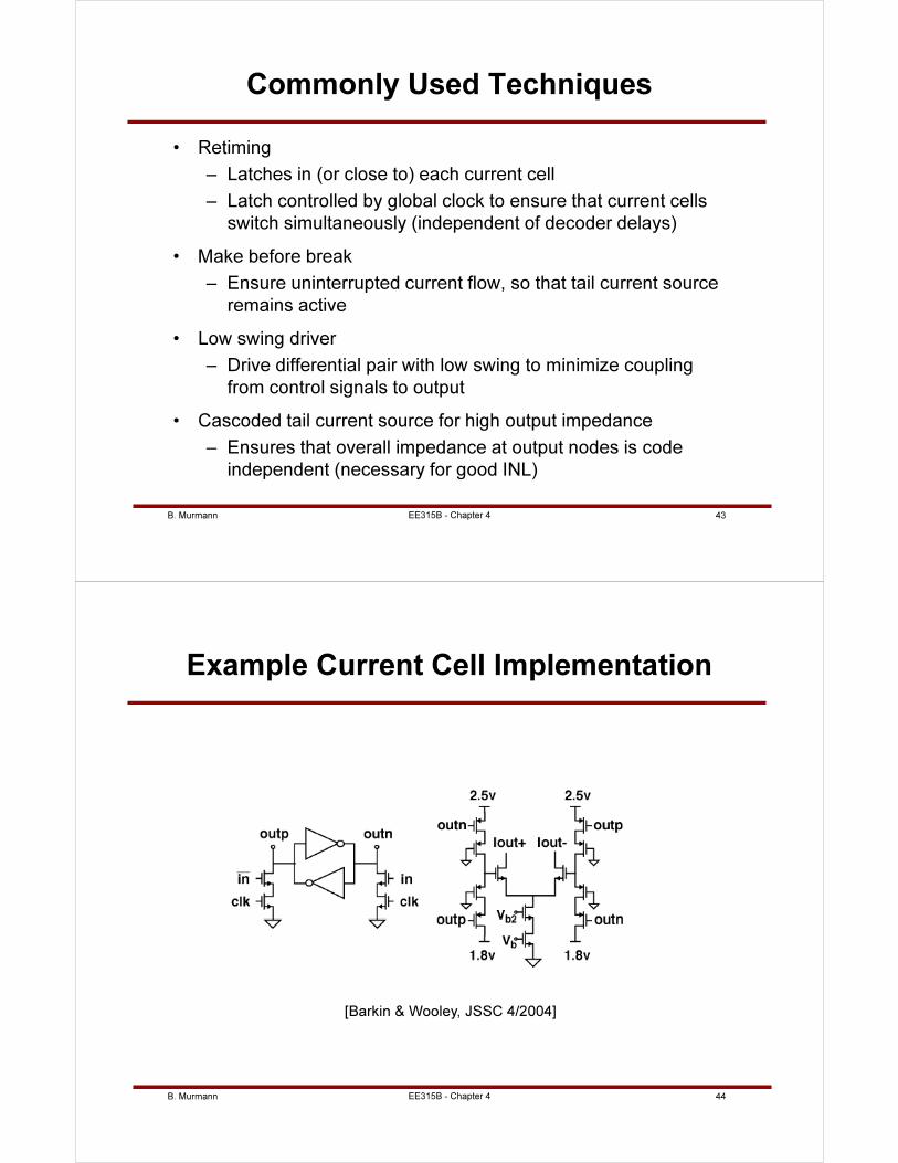
B. Murmann 43EE315B - Chapter 4
Commonly Used Techniques
• Retiming
– Latches in (or close to) each current cell
– Latch controlled by global clock to ensure that current cells
switch simultaneously (independent of decoder delays)
• Make before break
– Ensure uninterrupted current flow, so that tail current source
remains active
• Low swing driver
– Drive differential pair with low swing to minimize coupling
from control signals to output
• Cascoded tail current source for high output impedance
– Ensures that overall impedance at output nodes is code
independent (necessary for good INL)
B. Murmann 44EE315B - Chapter 4
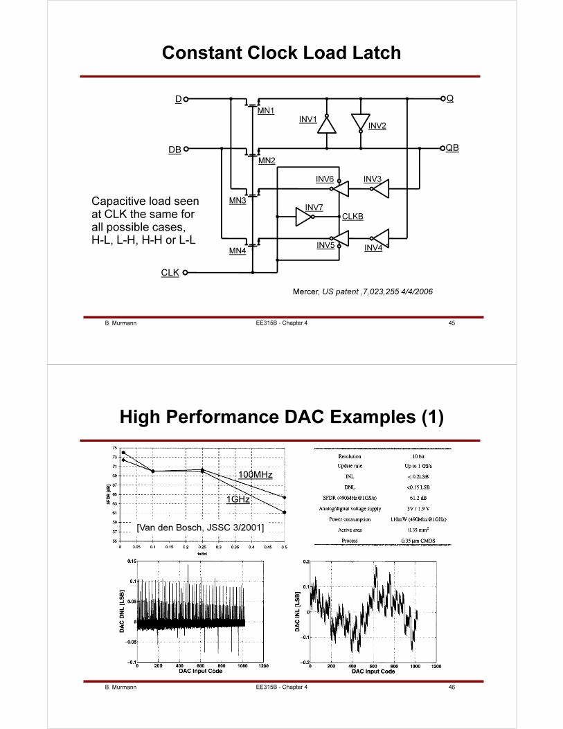
Example Current Cell Implementation
[Barkin & Wooley, JSSC 4/2004]
B. Murmann 45EE315B - Chapter 4
Constant Clock Load Latch
Mercer, US patent ,7,023,255 4/4/2006
DB
D
CLK
Q
QB
MN1
MN2
MN3
MN4
INV1INV2
INV3
INV4INV5
INV6
INV7
CLKB
Capacitive load seen at CLK the same for all possible cases,H-L, L-H, H-H or L-L
B. Murmann 46EE315B - Chapter 4
High Performance DAC Examples (1)
1GHz
100MHz
[Van den Bosch, JSSC 3/2001]
B. Murmann 47EE315B - Chapter 4
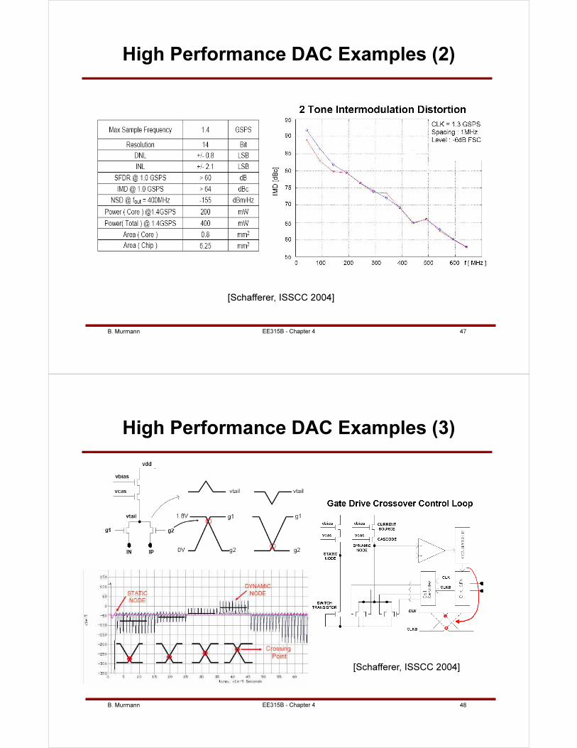
High Performance DAC Examples (2)
[Schafferer, ISSCC 2004]
B. Murmann 48EE315B - Chapter 4
High Performance DAC Examples (3)
[Schafferer, ISSCC 2004]
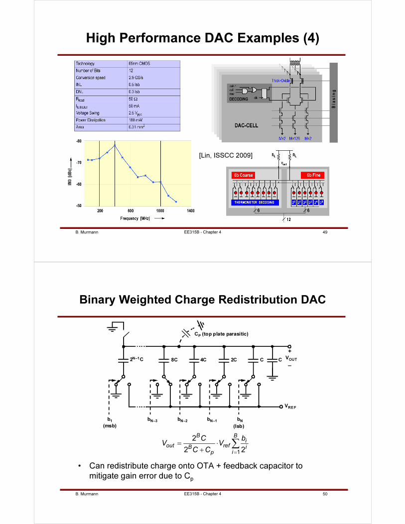
B. Murmann 49
High Performance DAC Examples (4)
EE315B - Chapter 4
[Lin, ISSCC 2009]
B. Murmann 50EE315B - Chapter 4
Binary Weighted Charge Redistribution DAC
• Can redistribute charge onto OTA + feedback capacitor to
mitigate gain error due to Cp
(msb)
8C 4C
(lsb)
VOUT
+
VREF
–
C2N–1C 2C C
b1 bN–3 bN–2 bN–1 bN
CP (top plate parasitic)
1
2
2 2
B Bi
out refB iip
bCV V
C C=
= ⋅
+
∑
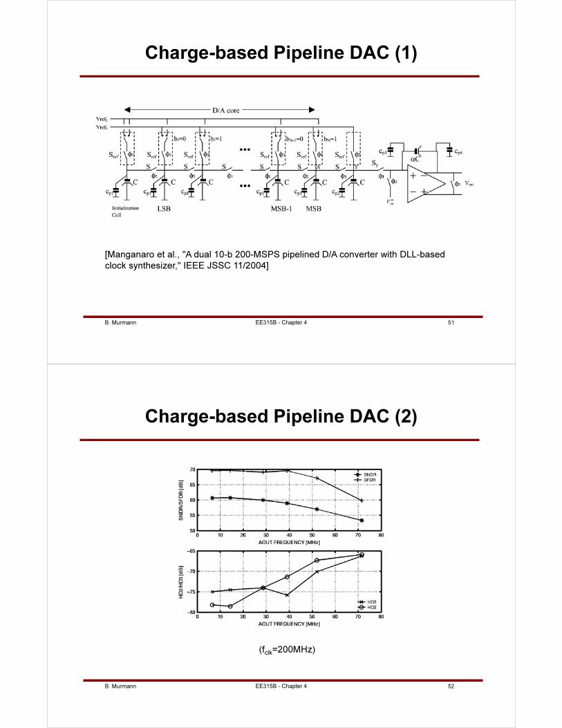
B. Murmann 51EE315B - Chapter 4
Charge-based Pipeline DAC (1)
[Manganaro et al., "A dual 10-b 200-MSPS pipelined D/A converter with DLL-based
clock synthesizer," IEEE JSSC 11/2004]
B. Murmann 52EE315B - Chapter 4
Charge-based Pipeline DAC (2)
(fclk=200MHz)
B. Murmann 1EE315B - Chapter 5
Sampling Circuits
Boris Murmann
Stanford University
Copyright © 2013 by Boris Murmann
B. Murmann 2EE315B - Chapter 5
Recap
• How to build circuits that "sample"?
• Ideal Dirac sampling is impractical
– Need a switch that opens, closes and acquires signal within
an infinitely small time
• Practical solution
– "Track and hold"
B. Murmann 3
Outline
• Elementary track-and-hold circuit and its nonidealities
• First order improvements to elementary track-and-hold
• Advanced techniques
– Clock bootstrapping
– Bottom plate sampling
• Settling and noise analysis in charge-redistribution
track-and-hold circuit
• Noise simulation example
EE315B - Chapter 5
B. Murmann 4
Ideal Track-and-Hold Circuit
EE315B - Chapter 5
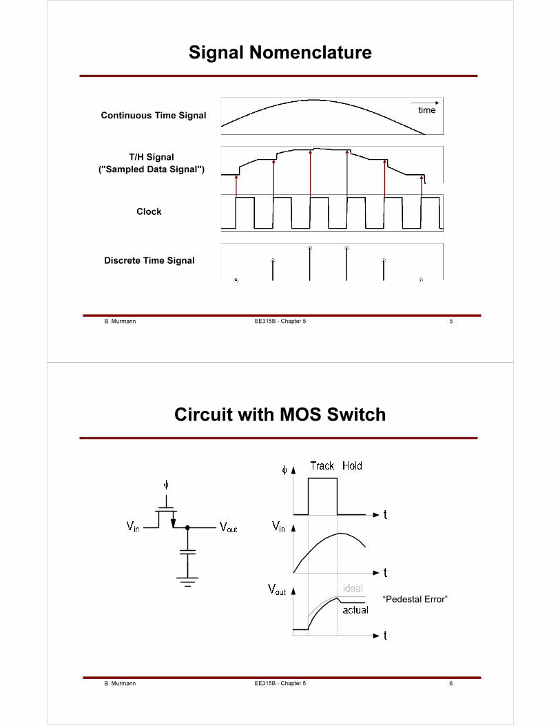
B. Murmann 5EE315B - Chapter 5
Signal Nomenclature
Continuous Time Signal
T/H Signal
("Sampled Data Signal")
Clock
Discrete Time Signal
time
B. Murmann 6
Circuit with MOS Switch
“Pedestal Error”
EE315B - Chapter 5
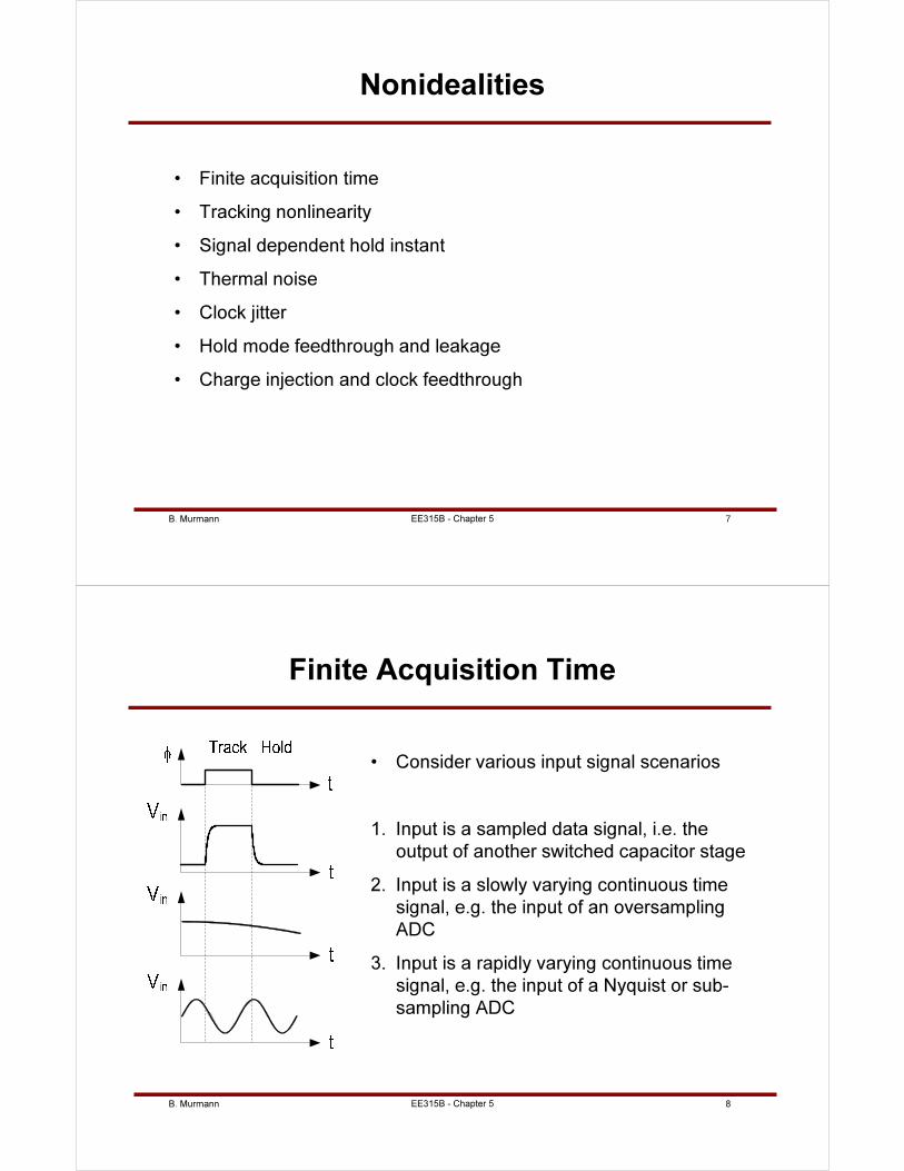
B. Murmann 7
Nonidealities
• Finite acquisition time
• Tracking nonlinearity
• Signal dependent hold instant
• Thermal noise
• Clock jitter
• Hold mode feedthrough and leakage
• Charge injection and clock feedthrough
EE315B - Chapter 5
B. Murmann 8
Finite Acquisition Time
• Consider various input signal scenarios
1. Input is a sampled data signal, i.e. the
output of another switched capacitor stage
2. Input is a slowly varying continuous time
signal, e.g. the input of an oversampling
ADC
3. Input is a rapidly varying continuous time
signal, e.g. the input of a Nyquist or sub-
sampling ADC
EE315B - Chapter 5
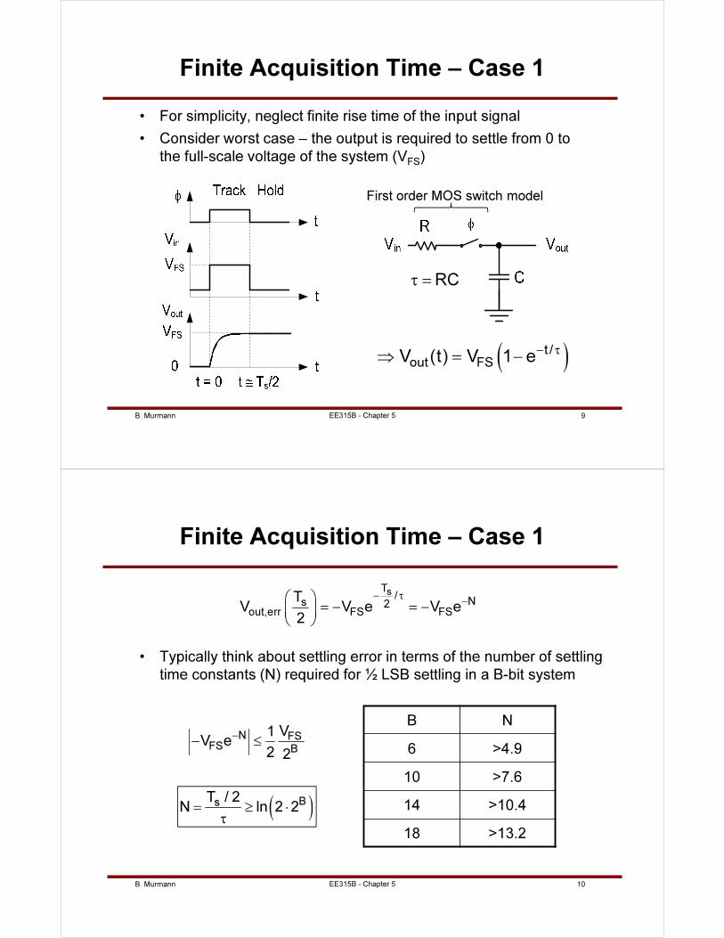
B. Murmann 9
Finite Acquisition Time – Case 1
• For simplicity, neglect finite rise time of the input signal
• Consider worst case – the output is required to settle from 0 to
the full-scale voltage of the system (VFS)
EE315B - Chapter 5
First order MOS switch model
( )t /
out FSV (t) V 1 e− τ
⇒ = −
RCτ =
B. Murmann 10
Finite Acquisition Time – Case 1
• Typically think about settling error in terms of the number of settling
time constants (N) required for ½ LSB settling in a B-bit system
EE315B - Chapter 5
B N
6 >4.9
10 >7.6
14 >10.4
18 >13.2
sT
/Ns 2
out,err FS FS
TV V e V e
2
− τ−
= − = −
N FSFS B
V1V e
2 2
−
− ≤
( )BsT / 2
N ln 2 2= ≥ ⋅
τ
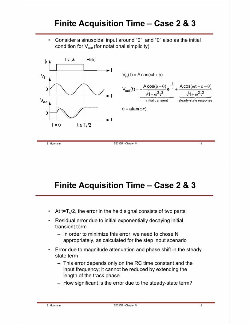
B. Murmann 11
Finite Acquisition Time – Case 2 & 3
• Consider a sinusoidal input around “0”, and “0” also as the initial
condition for Vout (for notational simplicity)
EE315B - Chapter 5
in
t
out2 2 2 2
initial transient steady-state response
V (t) Acos( t )
Acos( ) Acos( t )V (t) e
1 1
atan( )
−
τ
= ω + φ
φ − θ ω + φ − θ= − +
+ ω τ + ω τ
θ = ωτ
144424443 144424443
B. Murmann 12
Finite Acquisition Time – Case 2 & 3
• At t=Ts/2, the error in the held signal consists of two parts
• Residual error due to initial exponentially decaying initial
transient term
– In order to minimize this error, we need to chose N
appropriately, as calculated for the step input scenario
• Error due to magnitude attenuation and phase shift in the steady
state term
– This error depends only on the RC time constant and the
input frequency; it cannot be reduced by extending the
length of the track phase
– How significant is the error due to the steady-state term?
EE315B - Chapter 5
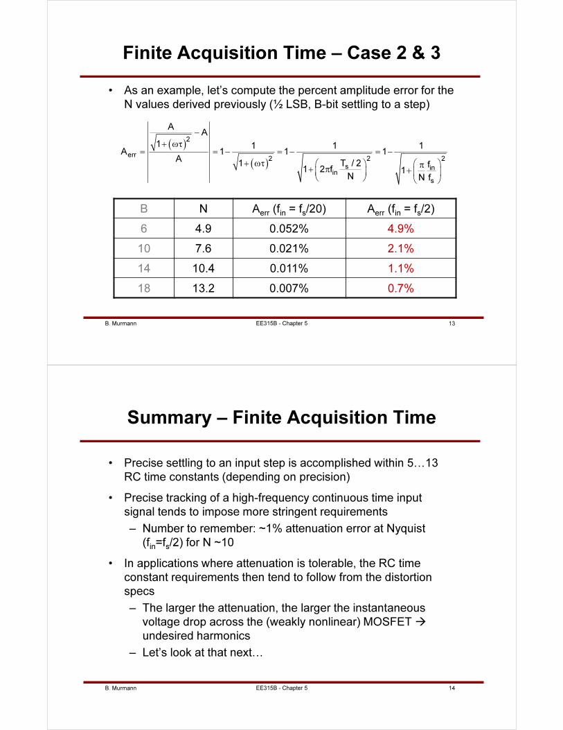
B. Murmann 13
Finite Acquisition Time – Case 2 & 3
• As an example, let’s compute the percent amplitude error for the
N values derived previously (½ LSB, B-bit settling to a step)
EE315B - Chapter 5
B N Aerr (fin = fs/20) Aerr (fin = fs/2)
6 4.9 0.052% 4.9%
10 7.6 0.021% 2.1%
14 10.4 0.011% 1.1%
18 13.2 0.007% 0.7%
( )
( )
2
err2 2 2
s inin
s
AA
1 1 1 1A 1 1 1
A1 T / 2 f
1 2 f 1N N f
−+ ωτ
= = − = − = −+ ωτ π+ π +
B. Murmann 14
Summary – Finite Acquisition Time
• Precise settling to an input step is accomplished within 5…13
RC time constants (depending on precision)
• Precise tracking of a high-frequency continuous time input
signal tends to impose more stringent requirements
– Number to remember: ~1% attenuation error at Nyquist
(fin=fs/2) for N ~10
• In applications where attenuation is tolerable, the RC time
constant requirements then tend to follow from the distortion
specs
– The larger the attenuation, the larger the instantaneous
voltage drop across the (weakly nonlinear) MOSFET
undesired harmonics
– Let’s look at that next…
EE315B - Chapter 5
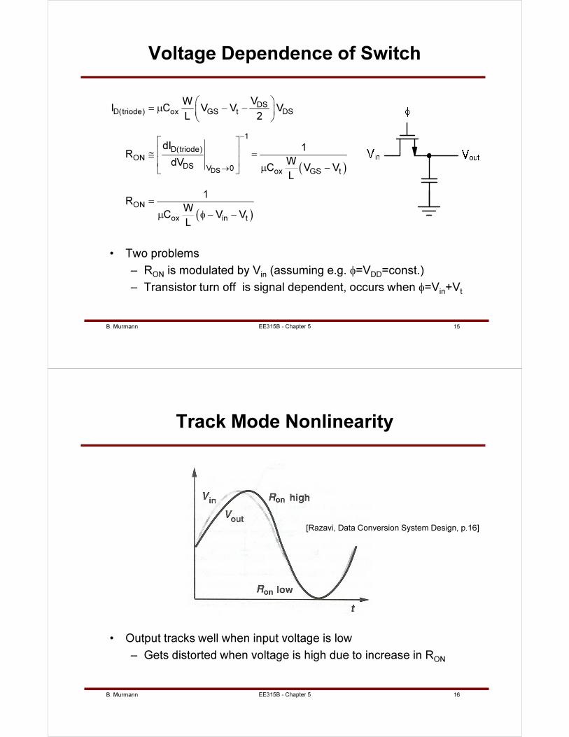
B. Murmann 15
Voltage Dependence of Switch
• Two problems
– RON is modulated by Vin (assuming e.g. φ=VDD=const.)
– Transistor turn off is signal dependent, occurs when φ=Vin+Vt
( )
( )
DS
DSD(triode) ox GS t DS
1
D(triode)ON
DS V 0 ox GS t
ON
ox in t
VWI C V V V
L 2
dI 1R
WdVC V V
L
1R
WC V V
L
−
→
= µ − −
≅ = µ −
=µ φ − −
EE315B - Chapter 5
B. Murmann 16
Track Mode Nonlinearity
• Output tracks well when input voltage is low
– Gets distorted when voltage is high due to increase in RON
EE315B - Chapter 5
[Razavi, Data Conversion System Design, p.16]
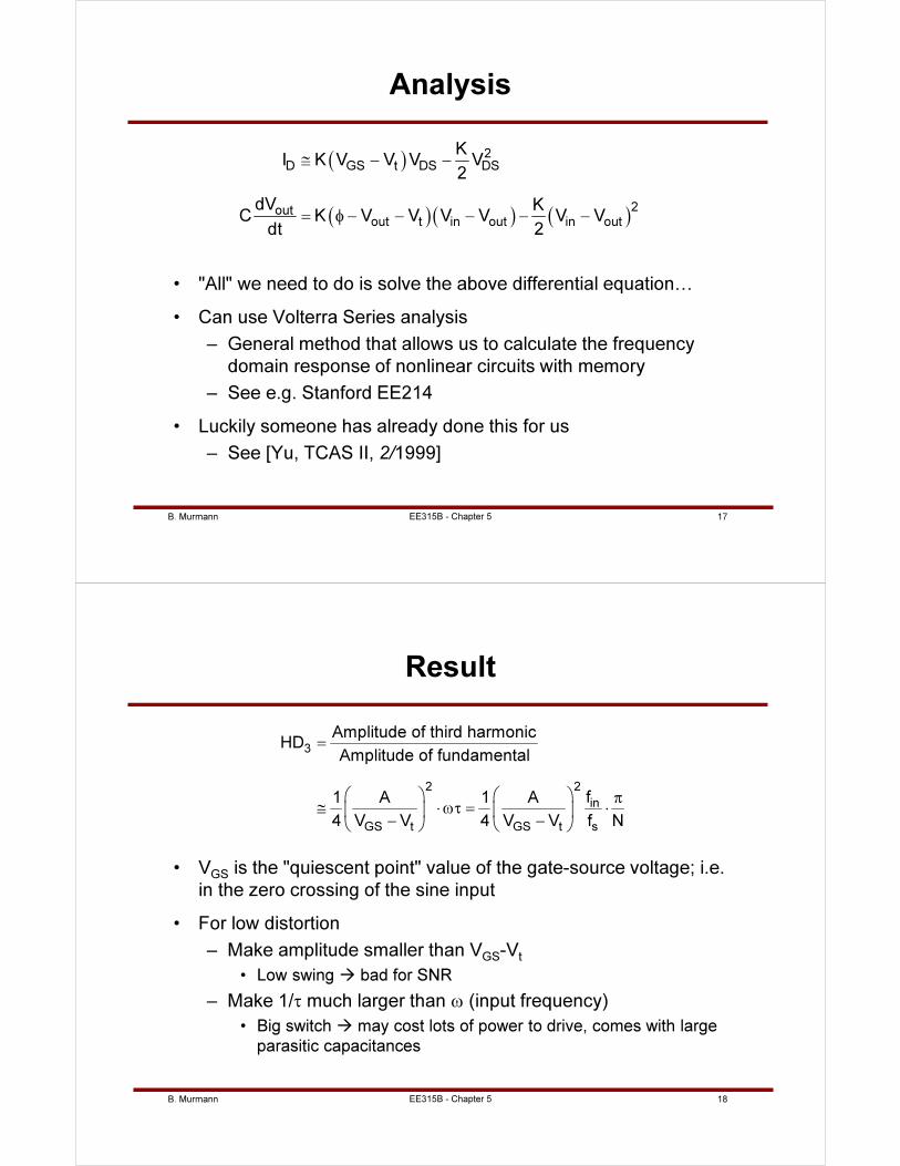
B. Murmann 17
Analysis
• "All" we need to do is solve the above differential equation…
• Can use Volterra Series analysis
– General method that allows us to calculate the frequency
domain response of nonlinear circuits with memory
– See e.g. Stanford EE214
• Luckily someone has already done this for us
– See [Yu, TCAS II, 2/1999]
( )
( )( ) ( )
2
D GS t DS DS
2outout t in out in out
KI K V V V V
2
dV KC K V V V V V V
dt 2
≅ − −
= φ − − − − −
EE315B - Chapter 5
B. Murmann 18
Result
• VGS is the "quiescent point" value of the gate-source voltage; i.e.
in the zero crossing of the sine input
• For low distortion
– Make amplitude smaller than VGS-Vt
• Low swing bad for SNR
– Make 1/τ much larger than ω (input frequency)
• Big switch may cost lots of power to drive, comes with large
parasitic capacitances
3
2 2
in
GS t GS t s
Amplitude of third harmonicHD
Amplitude of fundamental
f1 A 1 A
4 V V 4 V V f N
=
π≅ ⋅ωτ = ⋅
− −
EE315B - Chapter 5
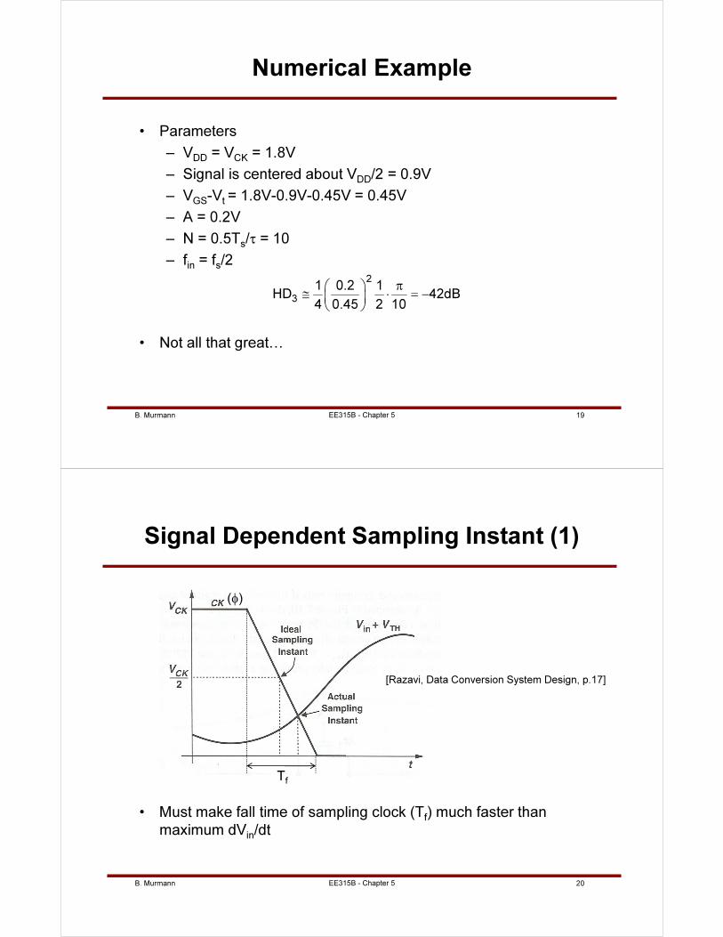
B. Murmann 19
Numerical Example
• Parameters
– VDD = VCK = 1.8V
– Signal is centered about VDD/2 = 0.9V
– VGS-Vt = 1.8V-0.9V-0.45V = 0.45V
– A = 0.2V
– N = 0.5Ts/τ = 10
– fin = fs/22
3
1 0.2 1HD 42dB
4 0.45 2 10
π ≅ ⋅ = −
EE315B - Chapter 5
• Not all that great…
B. Murmann 20
Signal Dependent Sampling Instant (1)
• Must make fall time of sampling clock (Tf) much faster than
maximum dVin/dt
[Razavi, Data Conversion System Design, p.17]
EE315B - Chapter 5
(φ)
Tf
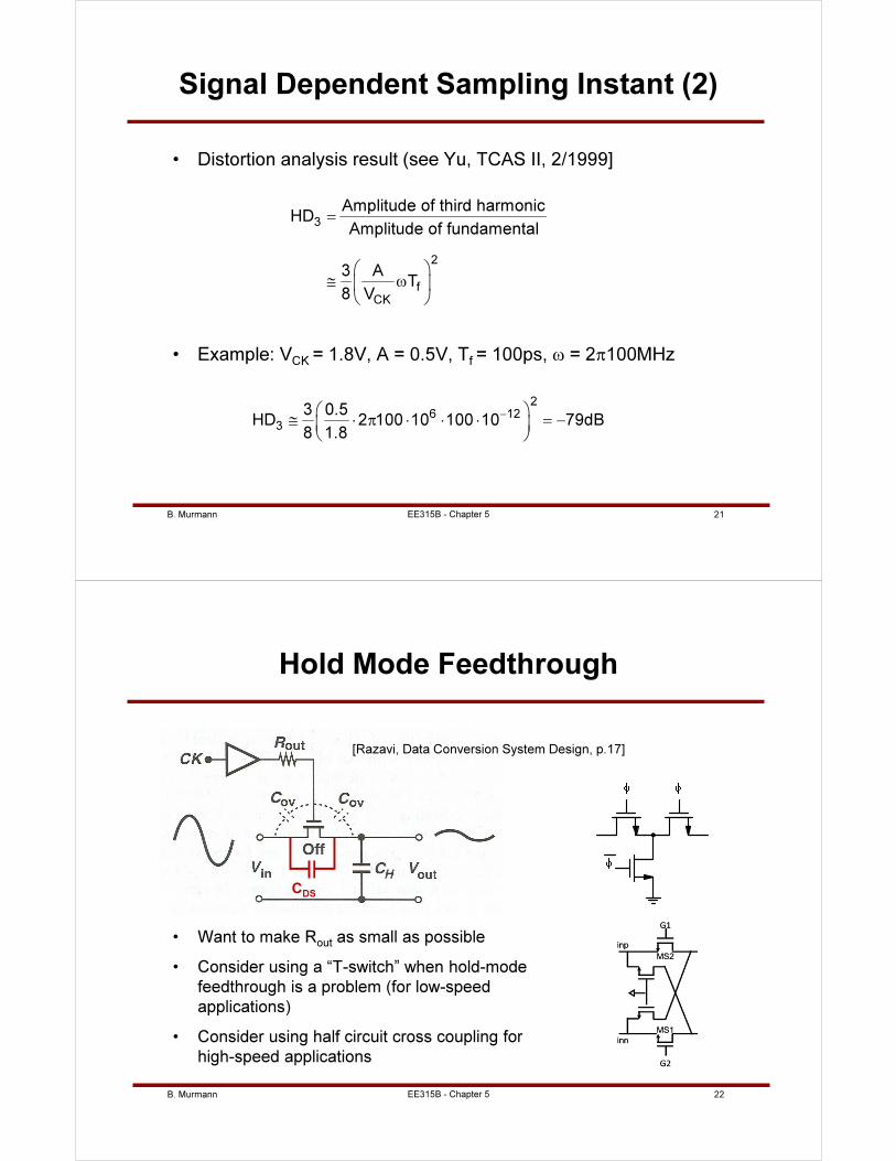
B. Murmann 21
Signal Dependent Sampling Instant (2)
• Distortion analysis result (see Yu, TCAS II, 2/1999]
EE315B - Chapter 5
3
2
f
CK
Amplitude of third harmonicHD
Amplitude of fundamental
3 AT
8 V
=
≅ ω
• Example: VCK = 1.8V, A = 0.5V, Tf = 100ps, ω = 2π100MHz
2
6 12
3
3 0.5HD 2 100 10 100 10 79dB
8 1.8
−
≅ ⋅ π ⋅ ⋅ ⋅ = −
B. Murmann 22
Hold Mode Feedthrough
• Want to make Rout as small as possible
• Consider using a “T-switch” when hold-mode
feedthrough is a problem (for low-speed
applications)
• Consider using half circuit cross coupling for
high-speed applications
CDS
[Razavi, Data Conversion System Design, p.17]
EE315B - Chapter 5
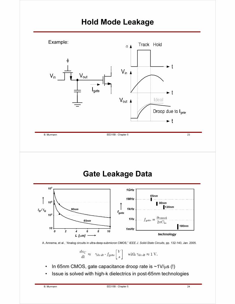
B. Murmann 23
Hold Mode Leakage
EE315B - Chapter 5
Example:
B. Murmann 24
Gate Leakage Data
• In 65nm CMOS, gate capacitance droop rate is ~1V/µs (!)
• Issue is solved with high-k dielectrics in post-65nm technologies
EE315B - Chapter 5
A. Annema, et al., “Analog circuits in ultra-deep-submicron CMOS,” IEEE J. Solid-State Circuits, pp. 132-143, Jan. 2005.
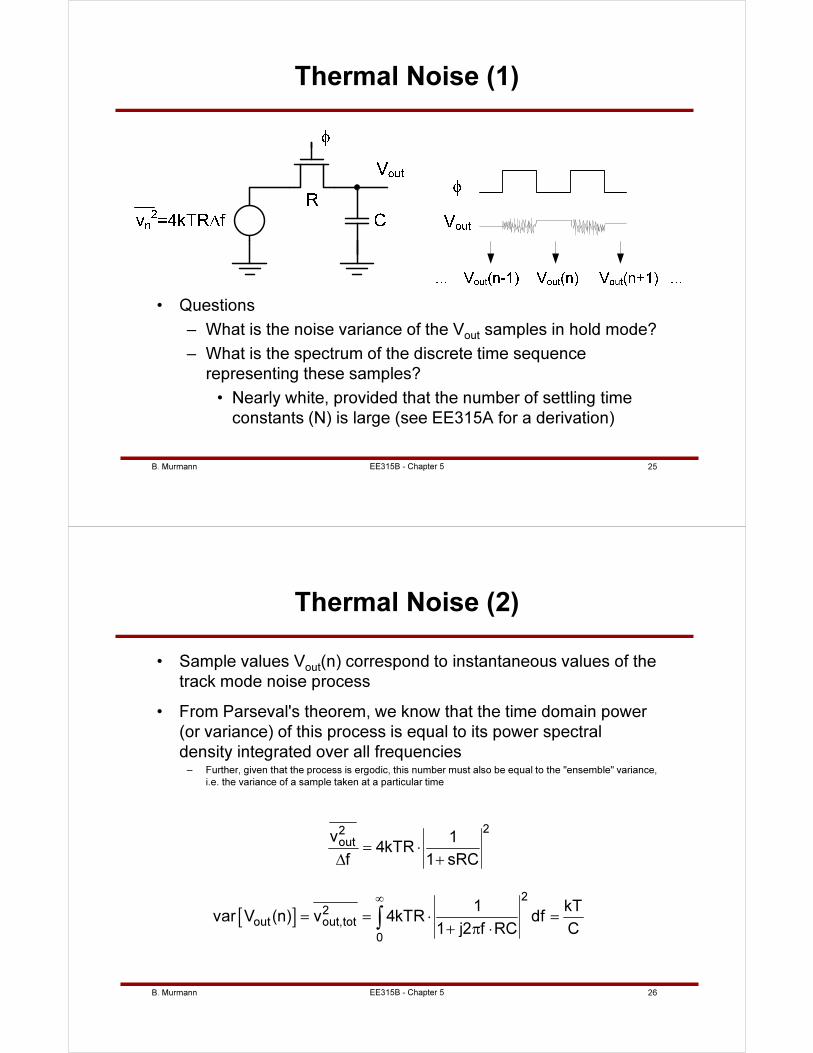
B. Murmann 25
Thermal Noise (1)
• Questions
– What is the noise variance of the Vout samples in hold mode?
– What is the spectrum of the discrete time sequence
representing these samples?
• Nearly white, provided that the number of settling time
constants (N) is large (see EE315A for a derivation)
EE315B - Chapter 5
B. Murmann 26
Thermal Noise (2)
• Sample values Vout(n) correspond to instantaneous values of the
track mode noise process
• From Parseval's theorem, we know that the time domain power
(or variance) of this process is equal to its power spectral
density integrated over all frequencies– Further, given that the process is ergodic, this number must also be equal to the "ensemble" variance,
i.e. the variance of a sample taken at a particular time
22
outv 1
4kTRf 1 sRC
= ⋅∆ +
[ ]2
2out out,tot
0
1 kTvar V (n) v 4kTR df
1 j2 f RC C
∞
= = ⋅ =
+ π ⋅∫
EE315B - Chapter 5
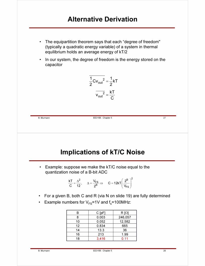
B. Murmann 27
Alternative Derivation
• The equipartition theorem says that each “degree of freedom"
(typically a quadratic energy variable) of a system in thermal
equilibrium holds an average energy of kT/2
• In our system, the degree of freedom is the energy stored on the
capacitor
2
out
2
out
1 1Cv kT
2 2
kTv
C
=
=
EE315B - Chapter 5
B. Murmann 28
Implications of kT/C Noise
• Example: suppose we make the kT/C noise equal to the
quantization noise of a B-bit ADC
22 B
FS
BFS
VkT 2, C 12kT
C 12 V2
∆= ∆ = ⇒ =
B C [pF] R [Ω]
8 0.003 246,057
10 0.052 12,582
12 0.834 665
14 13.3 36
16 213 1.99
18 3,416 0.11
• For a given B, both C and R (via N on slide 19) are fully determined
• Example numbers for VFS=1V and fs=100MHz:
EE315B - Chapter 5
B. Murmann 29
Commercial Example
EE315B - Chapter 5
B. Murmann 30
How to Estimate Thermal Noise
in the Lab?
• One option is to look at the measured SNR and back-calculate
the thermal component by subtraction of quantization noise and
DNL noise
• Another (potentially better) option is to take a code histogram
with “grounded input”
EE315B - Chapter 5
S. Ruscak and L. Singer, “Using Histogram
Techniques to Measure A/D Converter Noise”
http://www.analog.com/library/analogDialogue/
archives/29-2/cnvtrnoise.html
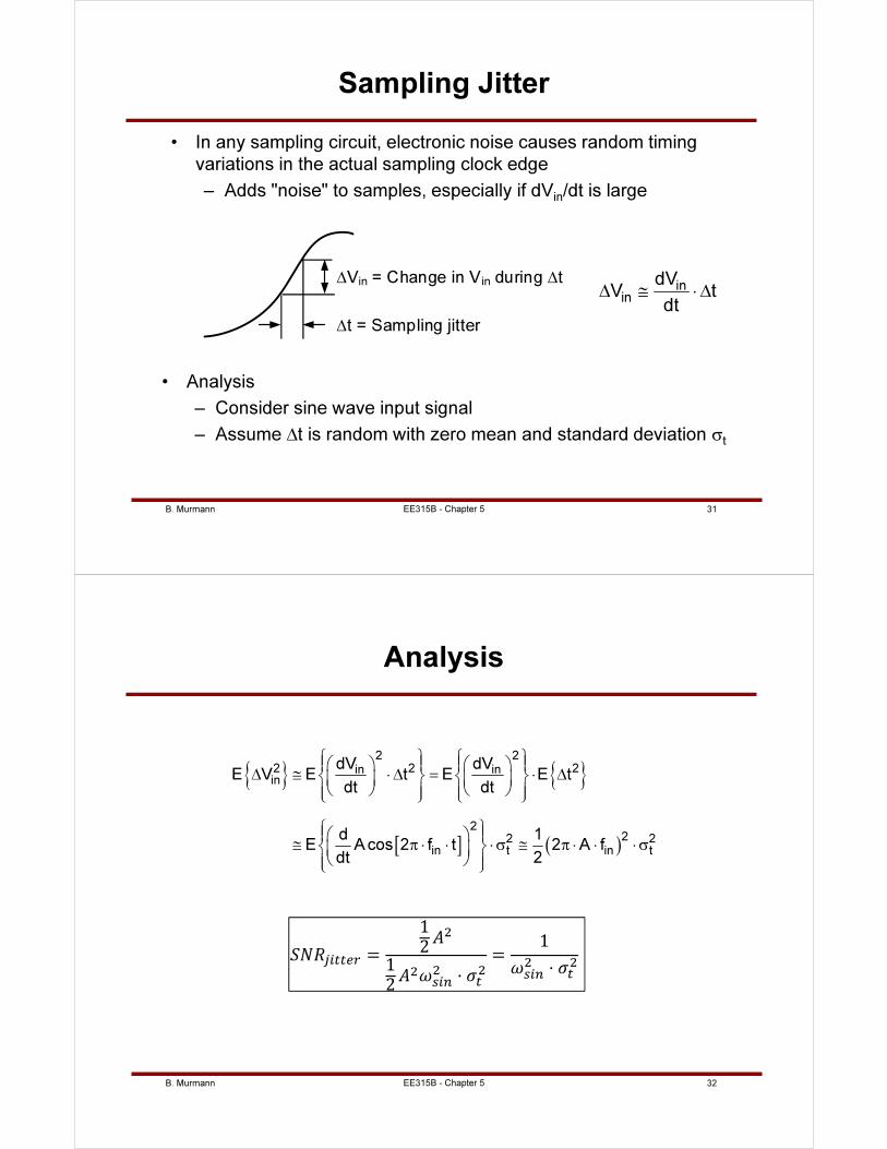
B. Murmann 31
Sampling Jitter
• In any sampling circuit, electronic noise causes random timing
variations in the actual sampling clock edge
– Adds "noise" to samples, especially if dVin/dt is large
∆Vin = Change in V in during ∆t
∆t = Sampling jitter
• Analysis
– Consider sine wave input signal
– Assume ∆t is random with zero mean and standard deviation σt
inin
dVV t
dt∆ ≅ ⋅ ∆
EE315B - Chapter 5
B. Murmann 32
Analysis
EE315B - Chapter 5
[ ] ( )
2 2
2 2 2in inin
222 2
in t in t
dV dVE V E t E E t
dt dt
d 1E Acos 2 f t 2 A f
dt 2
∆ ≅ ⋅ ∆ = ⋅ ∆
≅ π ⋅ ⋅ ⋅ σ ≅ π ⋅ ⋅ ⋅ σ
=
12
12
⋅ =
1
⋅
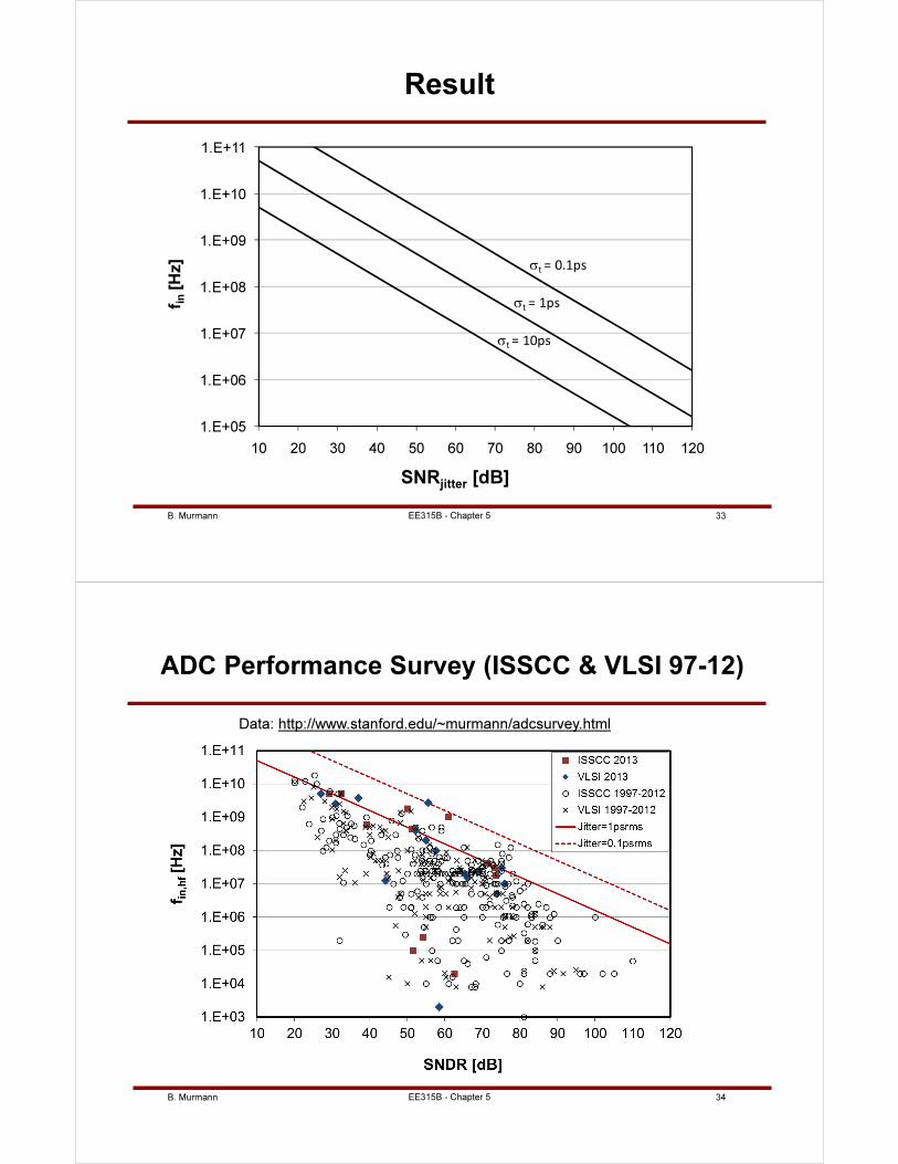
B. Murmann 33
Result
EE315B - Chapter 5
1.E+05
1.E+06
1.E+07
1.E+08
1.E+09
1.E+10
1.E+11
10 20 30 40 50 60 70 80 90 100 110 120
f in[H
z]
SNRaperture [dB]
σt= 0.1ps
σt= 1ps
σt= 10ps
SNRjitter [dB]
B. Murmann 34
ADC Performance Survey (ISSCC & VLSI 97-12)
Data: http://www.stanford.edu/~murmann/adcsurvey.html
EE315B - Chapter 5
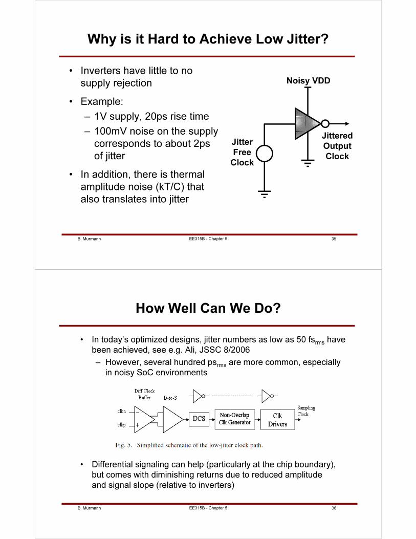
B. Murmann 35EE315B - Chapter 5
Why is it Hard to Achieve Low Jitter?
• Inverters have little to no
supply rejection
• Example:
– 1V supply, 20ps rise time
– 100mV noise on the supply
corresponds to about 2ps
of jitter
• In addition, there is thermal
amplitude noise (kT/C) that
also translates into jitter
Noisy VDD
Jitter
Free
Clock
Jittered
Output
Clock
B. Murmann 36
How Well Can We Do?
• In today’s optimized designs, jitter numbers as low as 50 fsrms have
been achieved, see e.g. Ali, JSSC 8/2006
– However, several hundred psrms are more common, especially
in noisy SoC environments
EE315B - Chapter 5
• Differential signaling can help (particularly at the chip boundary),
but comes with diminishing returns due to reduced amplitude
and signal slope (relative to inverters)
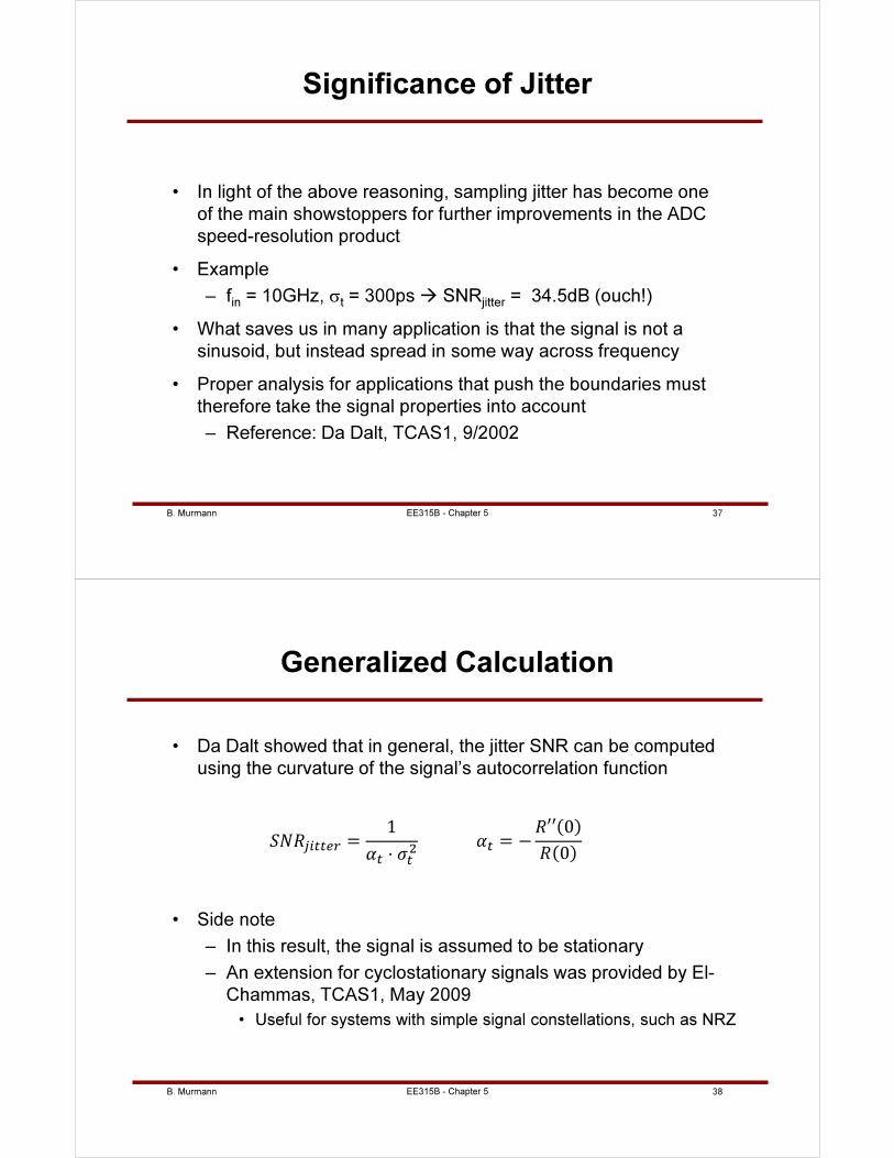
B. Murmann 37
Significance of Jitter
• In light of the above reasoning, sampling jitter has become one
of the main showstoppers for further improvements in the ADC
speed-resolution product
• Example
– fin = 10GHz, σt = 300ps SNRjitter = 34.5dB (ouch!)
• What saves us in many application is that the signal is not a
sinusoid, but instead spread in some way across frequency
• Proper analysis for applications that push the boundaries must
therefore take the signal properties into account
– Reference: Da Dalt, TCAS1, 9/2002
EE315B - Chapter 5
B. Murmann 38
Generalized Calculation
• Da Dalt showed that in general, the jitter SNR can be computed
using the curvature of the signal’s autocorrelation function
= −′′ 0
0 =
1
⋅
• Side note
– In this result, the signal is assumed to be stationary
– An extension for cyclostationary signals was provided by El-
Chammas, TCAS1, May 2009
• Useful for systems with simple signal constellations, such as NRZ
EE315B - Chapter 5
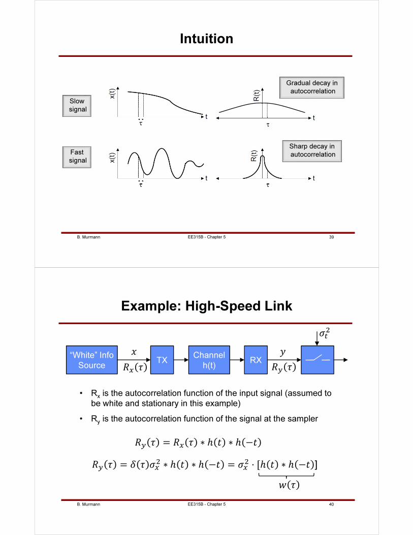
B. Murmann 39
Intuition
Slow
signal
Fast
signal
Sharp decay in
autocorrelation
Gradual decay in
autocorrelation
EE315B - Chapter 5
B. Murmann 40
Example: High-Speed Link
• Rx is the autocorrelation function of the input signal (assumed to
be white and stationary in this example)
• Ry is the autocorrelation function of the signal at the sampler
Channel
h(t)TX RX
“White” Info
Source
= ∗ ℎ ∗ ℎ −
= ∗ ℎ ∗ ℎ − =
⋅ [ℎ ∗ ℎ − ]
EE315B - Chapter 5
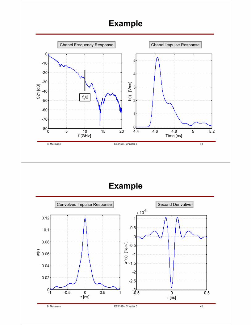
B. Murmann 41
Example
0 5 10 15 20-80
-70
-60
-50
-40
-30
-20
-10
0
f [GHz]
S21 [dB
]
4.4 4.6 4.8 5 5.20
1
2
3
4
5
Time [ns]
h(t
) [V
/ns]
Chanel Frequency Response Chanel Impulse Response
fs/2
EE315B - Chapter 5
B. Murmann 42
Example
Convolved Impulse Response Second Derivative
-1 -0.5 0 0.5 10
0.02
0.04
0.06
0.08
0.1
0.12
τ [ns]
w(τ)
-0.5 0 0.5-3
-2.5
-2
-1.5
-1
-0.5
0
0.5
1
x 10-5
τ [ns]
w''(τ)
[1
/ps2]
EE315B - Chapter 5
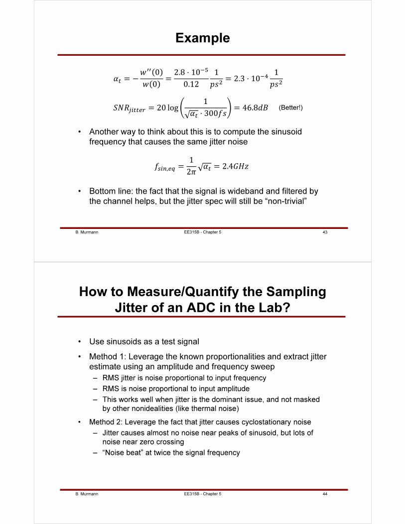
B. Murmann 43
Example
• Another way to think about this is to compute the sinusoid
frequency that causes the same jitter noise
= − 0
0=
2.8 ⋅ 10
0.12
1
= 2.3 ⋅ 10
1
, =1
2 = 2.4
(Better!)
• Bottom line: the fact that the signal is wideband and filtered by
the channel helps, but the jitter spec will still be “non-trivial”
EE315B - Chapter 5
= 20 log1
⋅ 300= 46.8
B. Murmann 44
How to Measure/Quantify the Sampling
Jitter of an ADC in the Lab?
• Use sinusoids as a test signal
• Method 1: Leverage the known proportionalities and extract jitter
estimate using an amplitude and frequency sweep
– RMS jitter is noise proportional to input frequency
– RMS is noise proportional to input amplitude
– This works well when jitter is the dominant issue, and not masked
by other nonidealities (like thermal noise)
• Method 2: Leverage the fact that jitter causes cyclostationary noise
– Jitter causes almost no noise near peaks of sinusoid, but lots of
noise near zero crossing
– “Noise beat” at twice the signal frequency
EE315B - Chapter 5
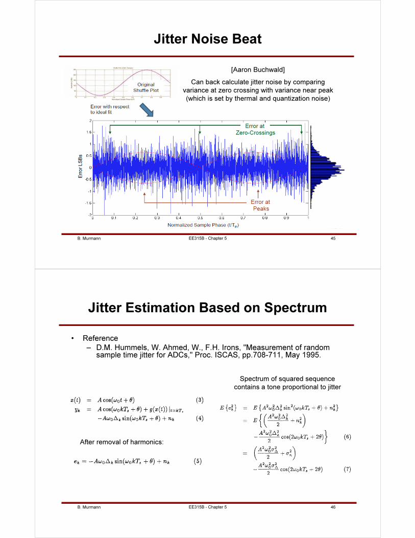
B. Murmann 45
Jitter Noise Beat
EE315B - Chapter 5
[Aaron Buchwald]
Can back calculate jitter noise by comparing
variance at zero crossing with variance near peak
(which is set by thermal and quantization noise)
B. Murmann 46
Jitter Estimation Based on Spectrum
• Reference
– D.M. Hummels, W. Ahmed, W., F.H. Irons, "Measurement of random sample time jitter for ADCs," Proc. ISCAS, pp.708-711, May 1995.
After removal of harmonics:
Spectrum of squared sequence
contains a tone proportional to jitter
EE315B - Chapter 5
B. Murmann 47
Matlab Code
% Jitter estimation technique proposed by Hummels, ISCAS 1995
% x is a vector that contains an integer number of cycles of a sampled sine wave
function [sigma_jitter_est, sigma_noise_est, fsin] = estimate_jitter(x, show_plot)
% take fft, remove DC, signal and harmonics
N = length(x);
s = fft(x);
[sigamp, sigbin]=max(abs(s));
A_est = sigamp/N*2;
cycles = sigbin-1;
fsin = cycles/N;
harmbins = 1 + abs([2:8]*cycles - N*round([2:8]*cycles/N));
sn=s;
sn(1)=eps;
sn(sigbin)=eps;
sn(N+2-sigbin)=eps;
sn(harmbins) =eps;
sn(N+2-harmbins)=eps;
% inverse fft, compute jitter and noise estimates
xinv = ifft(sn, 'symmetric');
s_inv = abs(fft(xinv.^2));
jitterbin = 1 + abs(2*cycles - N*round(2*cycles/N));
sigma_jitter_est = sqrt(2*2*s_inv(jitterbin)/N/(2*pi*fsin)^2/A_est^2);
sigma_noise_est = sqrt(s_inv(1)/N-2*s_inv(jitterbin)/N);
EE315B - Chapter 5
B. Murmann 48
Charge Injection and Clock Feedthrough
• Analyze two extreme cases
– Very large Tf (“slow gating”)
– Very small Tf (“fast gating”)
EE315B - Chapter 5
“Pedestal Error”
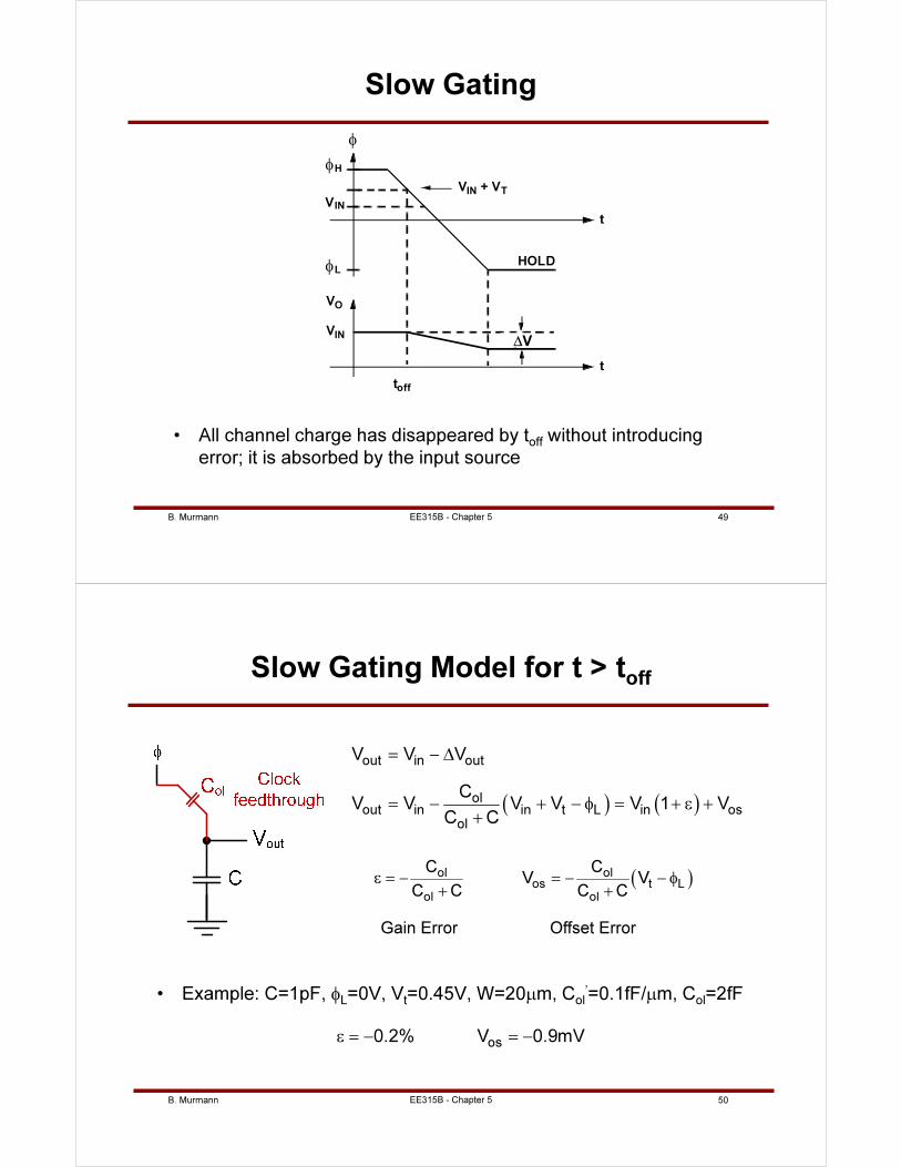
B. Murmann 49
Slow Gating
• All channel charge has disappeared by toff without introducing
error; it is absorbed by the input source
t
φ
φL
φH
HOLD
VIN
VO
VIN
VIN + VT
toff
ýV
t
∆V
EE315B - Chapter 5
B. Murmann 50
Slow Gating Model for t > toff
• Example: C=1pF, φL=0V, Vt=0.45V, W=20µm, Col’=0.1fF/µm, Col=2fF
( ) ( )
out in out
olout in in t L in os
ol
V V V
CV V V V V 1 V
C C
= − ∆
= − + − φ = + ε ++
EE315B - Chapter 5
( )ol olos t L
ol ol
C CV V
C C C Cε = − = − − φ
+ +
Gain Error Offset Error
os0.2% V 0.9mVε = − = −
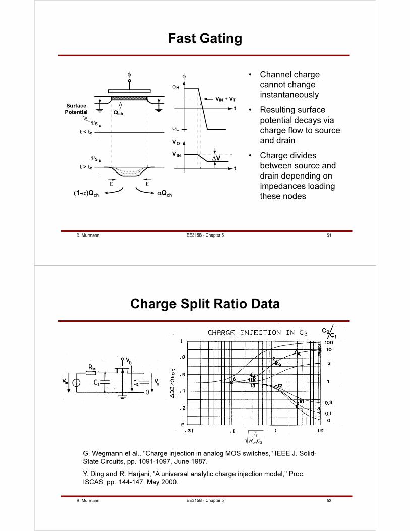
B. Murmann 51
Fast Gating
• Channel charge
cannot change
instantaneously
• Resulting surface
potential decays via
charge flow to source
and drain
• Charge divides
between source and
drain depending on
impedances loading
these nodes
φ
Qch
Qch12
Qch12
t < to
t > to
Ε Ε
ΨS
ΨS
t
φ
φL
φH
V IN
VO
VIN + VT
ýV
t
Surface
Potential
∆V
αQch(1-α)Qch
EE315B - Chapter 5
B. Murmann 52
Charge Split Ratio Data
2
f
on
T
R C
G. Wegmann et al., "Charge injection in analog MOS switches," IEEE J. Solid-
State Circuits, pp. 1091-1097, June 1987.
Y. Ding and R. Harjani, "A universal analytic charge injection model," Proc.
ISCAS, pp. 144-147, May 2000.
EE315B - Chapter 5
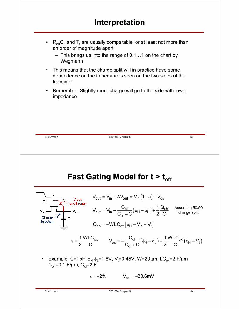
B. Murmann 53
Interpretation
• RonC2 and Tf are usually comparable, or at least not more than
an order of magnitude apart
– This brings us into the range of 0.1…1 on the chart by
Wegmann
• This means that the charge split will in practice have some
dependence on the impedances seen on the two sides of the
transistor
• Remember: Slightly more charge will go to the side with lower
impedance
EE315B - Chapter 5
B. Murmann 54
Fast Gating Model for t > toff
• Example: C=1pF, φH-φL=1.8V, Vt=0.45V, W=20µm, LCox=2fF/µm
Col’=0.1fF/µm, Col=2fF
( ) ( )ox ol oxos H L H t
ol
WLC C WLC1 1V V
2 C C C 2 Cε = = − φ − φ − φ −
+
EE315B - Chapter 5
os2% V 30.6mVε = + = −
Assuming 50/50
charge split
( )
( )
[ ]
out in out in os
ol chout in H L
ol
ch ox H in t
V V V V 1 V
C Q1V V
C C 2 C
Q WLC V V
= − ∆ = + ε +
= − φ − φ ++
= − φ − −
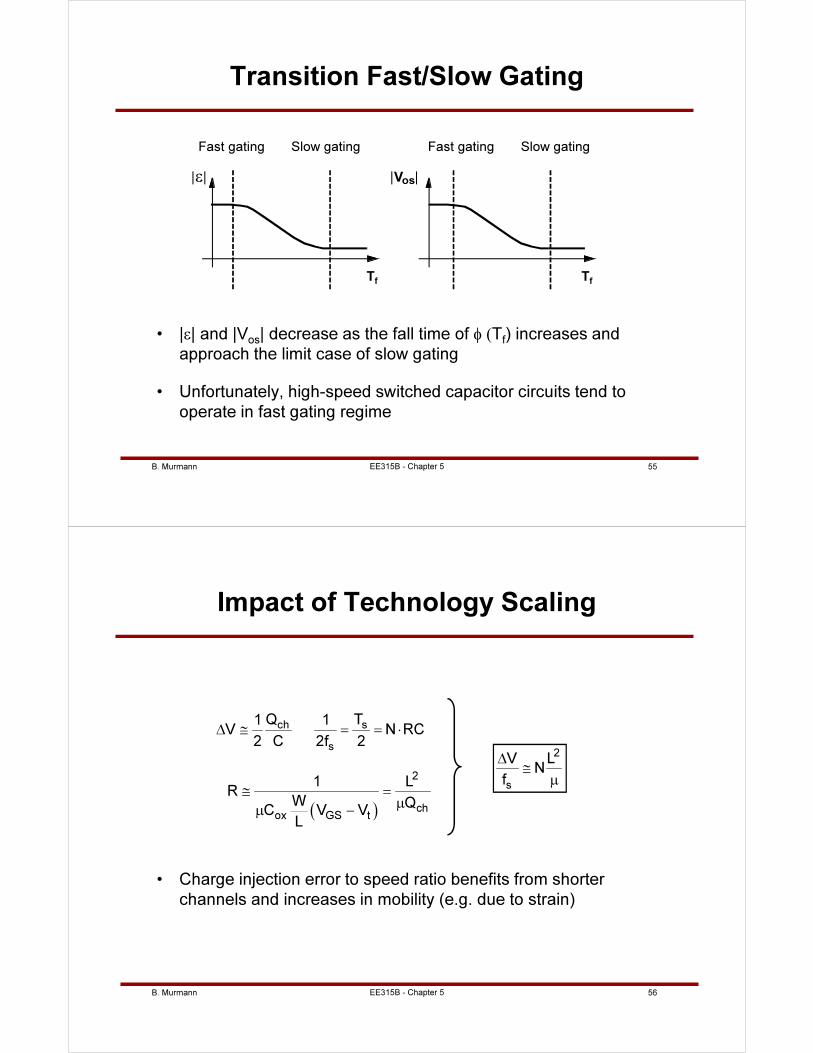
B. Murmann 55
Transition Fast/Slow Gating
• |ε| and |Vos| decrease as the fall time of φ (Tf) increases and
approach the limit case of slow gating
• Unfortunately, high-speed switched capacitor circuits tend to
operate in fast gating regime
tF
|ε| |Vos|
tF
EE315B - Chapter 5
Tf Tf
Fast gating Slow gating Fast gating Slow gating
B. Murmann 56
Impact of Technology Scaling
ch s
s
Q T1 1V N RC
2 C 2f 2∆ ≅ = = ⋅
( )
2
chox GS t
1 LR
W QC V V
L
≅ =µ
µ −
2
s
V LN
f
∆≅
µ
• Charge injection error to speed ratio benefits from shorter
channels and increases in mobility (e.g. due to strain)
EE315B - Chapter 5
B. Murmann 57
Outline
• Elementary track-and-hold circuit and its nonidealities
• First order improvements to elementary track-and-hold
• Advanced techniques
– Clock bootstrapping
– Bottom plate sampling
• Settling and noise analysis in charge-redistribution
track-and-hold circuit
• Noise simulation example
EE315B - Chapter 5
B. Murmann 58
Improvements
• Charge cancelation
– Try to cancel channel charge by injecting a charge packet
with opposite sign
• Differential sampling
– Use a differential circuit to suppress offset
• CMOS switch
– Try to balance the nonidealities of NMOS device with a
parallel PMOS
EE315B - Chapter 5
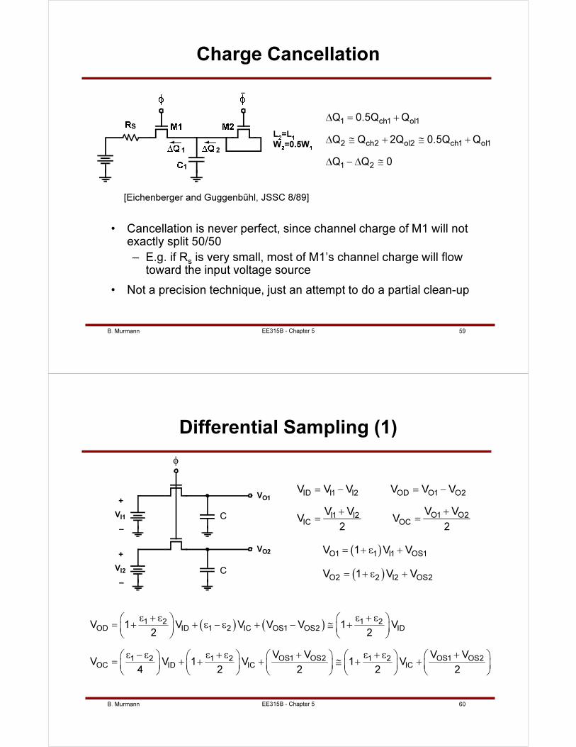
B. Murmann 59
Charge Cancellation
• Cancellation is never perfect, since channel charge of M1 will not exactly split 50/50
– E.g. if Rs is very small, most of M1’s channel charge will flow toward the input voltage source
• Not a precision technique, just an attempt to do a partial clean-up
S
1
1 2
L =L
W =0.5W
1 ch1 ol1
2 ch2 ol2 ch1 ol1
1 2
Q 0.5Q Q
Q Q 2Q 0.5Q Q
Q Q 0
∆ = +
∆ ≅ + ≅ +
∆ − ∆ ≅
EE315B - Chapter 5
[Eichenberger and Guggenbűhl, JSSC 8/89]
B. Murmann 60
Differential Sampling (1)
φ
VI1 CH
+
–
VO1
VI2 CH
+
–
VO2
ID I1 I2 OD O1 O2
O1 O2I1 I2IC OC
V V V V V V
V VV VV V
2 2
= − = −
++
= =
( )
( )
O1 1 I1 OS1
O2 2 I2 OS2
V 1 V V
V 1 V V
= + ε +
= + ε +
( ) ( )1 2 1 2OD ID 1 2 IC OS1 OS2 ID
OS1 OS2 OS1 OS21 2 1 2 1 2OC ID IC IC
V 1 V V V V 1 V2 2
V V V VV V 1 V 1 V
4 2 2 2 2
ε + ε ε + ε = + + ε − ε + − ≅ +
+ +ε − ε ε + ε ε + ε = + + + ≅ + +
EE315B - Chapter 5
C
C
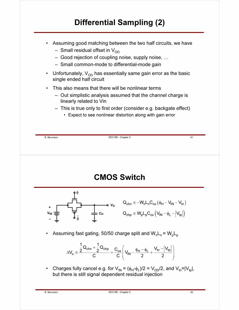
B. Murmann 61
Differential Sampling (2)
• Assuming good matching between the two half circuits, we have
– Small residual offset in VOD
– Good rejection of coupling noise, supply noise, …
– Small common-mode to differential-mode gain
• Unfortunately, VOD has essentially same gain error as the basic
single ended half circuit
• This also means that there will be nonlinear terms
– Out simplistic analysis assumed that the channel charge is
linearly related to Vin
– This is true only to first order (consider e.g. backgate effect)
• Expect to see nonlinear distortion along with gain error
EE315B - Chapter 5
B. Murmann 62
CMOS Switch
• Charges fully cancel e.g. for VIN = (φH-φL)/2 = VDD/2, and Vtn=|Vtp|,
but there is still signal dependent residual injection
φ
VIN
φ
CH
+
–
VO
( )
( )
chn n n ox H IN tn
chp p p ox IN L tp
Q W L C V V
Q W L C V V
≅ − φ − −
≅ − φ −
EE315B - Chapter 5
chn chp tn tpox H Lo IN
1 1Q Q V VC2 2V V
C C 2 2
+ −φ − φ ∆ ≅ = − +
• Assuming fast gating, 50/50 charge split and WnLn = WpLp
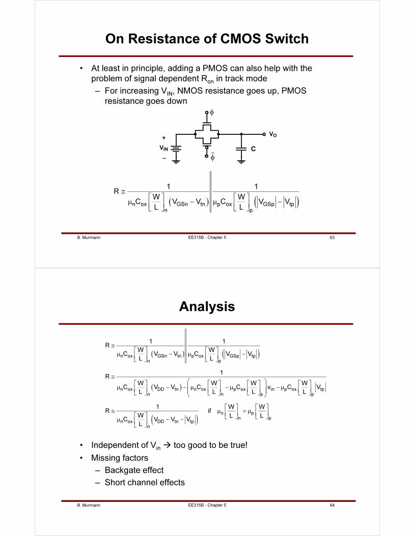
B. Murmann 63
On Resistance of CMOS Switch
• At least in principle, adding a PMOS can also help with the
problem of signal dependent Ron in track mode
– For increasing VIN, NMOS resistance goes up, PMOS
resistance goes down
EE315B - Chapter 5
( ) ( )n ox GSn tn p ox GSp tpn p
1 1R
W WC V V C V V
L L
≅ µ − µ −
φ
VIN
φ
CH
+
–
VO
C
B. Murmann 64
Analysis
• Independent of Vin too good to be true!
• Missing factors
– Backgate effect
– Short channel effects
( ) ( )
( )
( )
n ox GSn tn p ox GSp tpn p
n ox DD tn n ox p ox in p ox tpn n p p
n pn p
n ox DD tn tpn
1 1R
W WC V V C V V
L L
1R
W W W WC V V C C v C V
L L L L
1 W WR if
W L LC V V V
L
≅ µ − µ −
≅ µ − − µ − µ − µ
≅ µ = µ µ − −
EE315B - Chapter 5
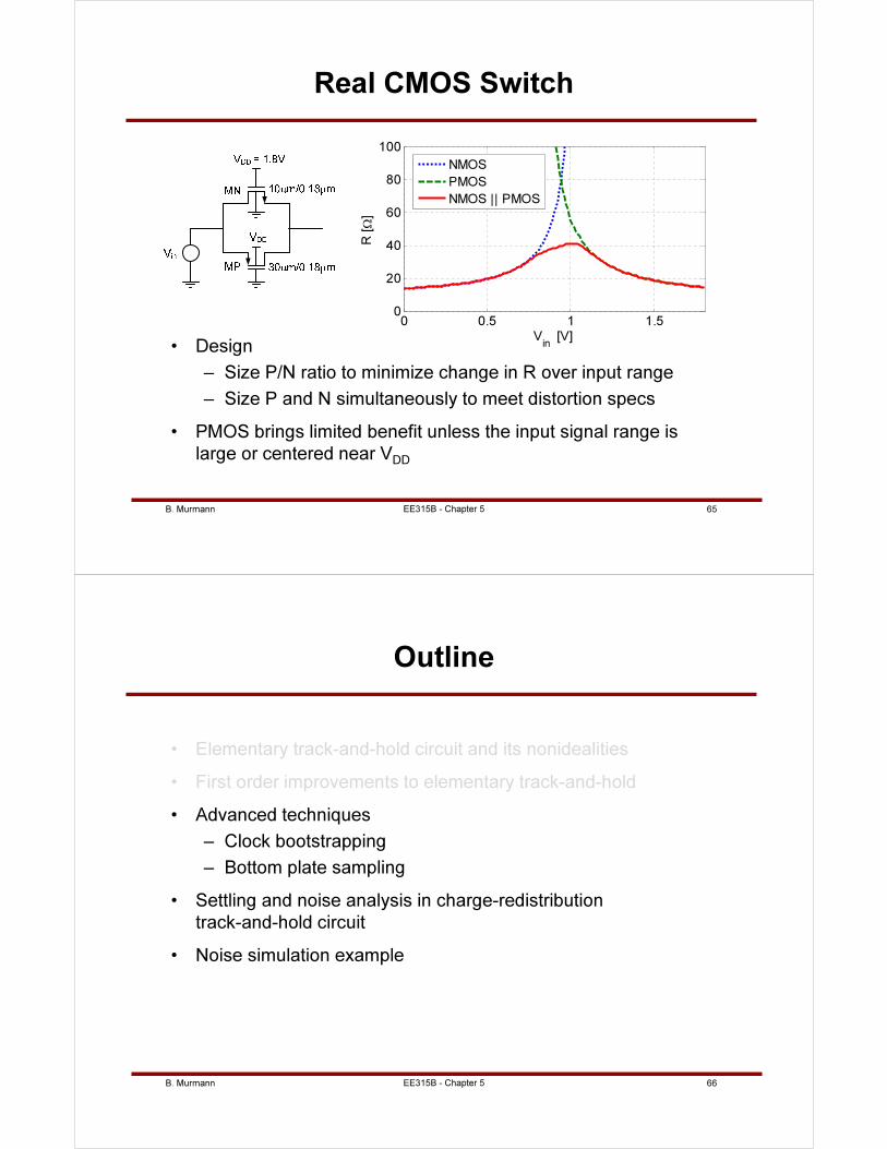
B. Murmann 65
Real CMOS Switch
• Design
– Size P/N ratio to minimize change in R over input range
– Size P and N simultaneously to meet distortion specs
• PMOS brings limited benefit unless the input signal range is
large or centered near VDD
EE315B - Chapter 5
0 0.5 1 1.50
20
40
60
80
100
Vin
[V]
R [Ω
]
NMOS
PMOS
NMOS || PMOS
B. Murmann 66
Outline
• Elementary track-and-hold circuit and its nonidealities
• First order improvements to elementary track-and-hold
• Advanced techniques
– Clock bootstrapping
– Bottom plate sampling
• Settling and noise analysis in charge-redistribution
track-and-hold circuit
• Noise simulation example
EE315B - Chapter 5
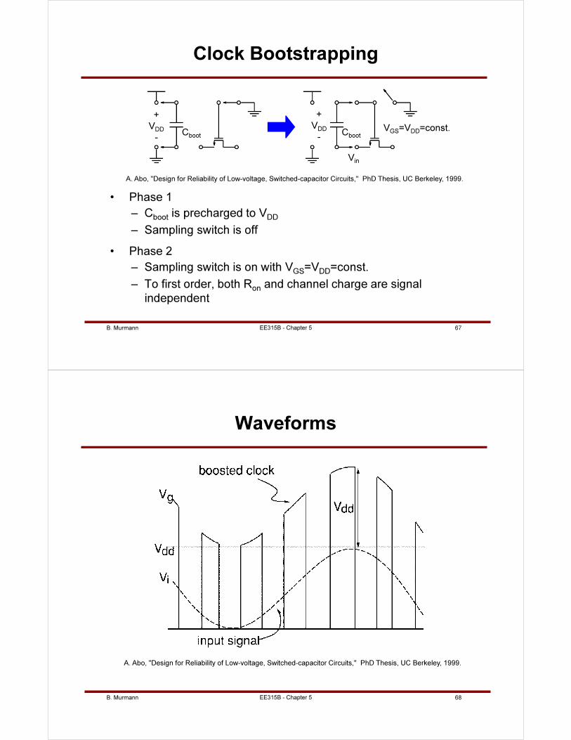
B. Murmann 67
Clock Bootstrapping
• Phase 1
– Cboot is precharged to VDD
– Sampling switch is off
• Phase 2
– Sampling switch is on with VGS=VDD=const.
– To first order, both Ron and channel charge are signal
independent
EE315B - Chapter 5
A. Abo, "Design for Reliability of Low-voltage, Switched-capacitor Circuits," PhD Thesis, UC Berkeley, 1999.
+
VDD
-
+
VDD
-
Vin
VGS=VDD=const.Cboot Cboot
B. Murmann 68
Waveforms
EE315B - Chapter 5
A. Abo, "Design for Reliability of Low-voltage, Switched-capacitor Circuits," PhD Thesis, UC Berkeley, 1999.
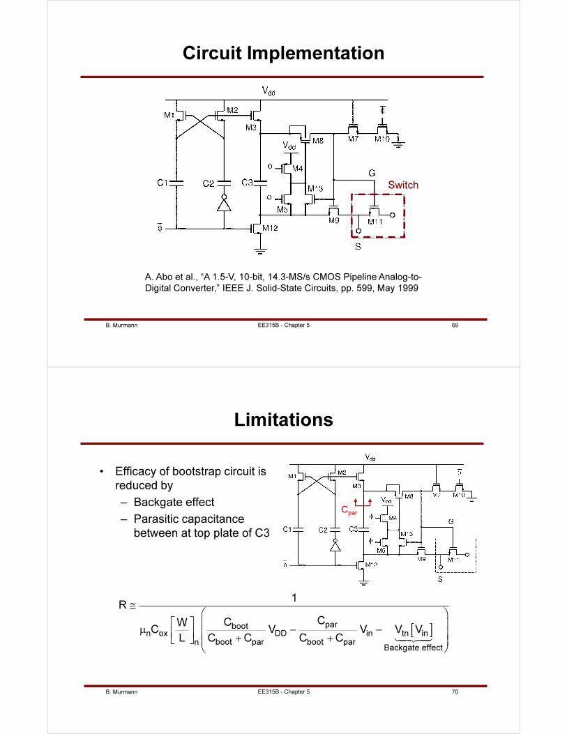
B. Murmann 69
Circuit Implementation
Switch
A. Abo et al., “A 1.5-V, 10-bit, 14.3-MS/s CMOS Pipeline Analog-to-
Digital Converter,” IEEE J. Solid-State Circuits, pp. 599, May 1999
EE315B - Chapter 5
B. Murmann 70
Limitations
• Efficacy of bootstrap circuit is
reduced by
– Backgate effect
– Parasitic capacitance
between at top plate of C3
[ ]parbootn ox DD in tn in
boot par boot parnBackgate effect
1R
CCWC V V V V
L C C C C
≅
µ − − + +
14243
EE315B - Chapter 5
Cpar
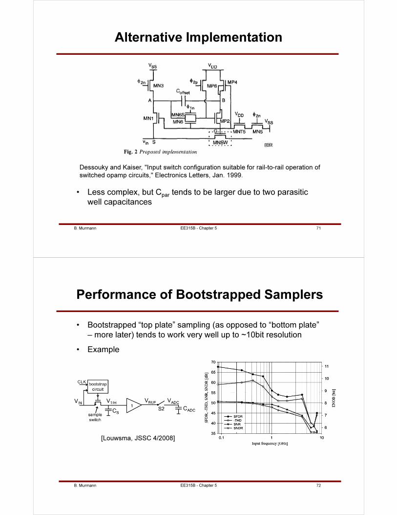
B. Murmann 71
Alternative Implementation
• Less complex, but Cpar tends to be larger due to two parasitic
well capacitances
EE315B - Chapter 5
Dessouky and Kaiser, "Input switch configuration suitable for rail-to-rail operation of
switched opamp circuits," Electronics Letters, Jan. 1999.
B. Murmann 72
Performance of Bootstrapped Samplers
• Bootstrapped “top plate” sampling (as opposed to “bottom plate”
– more later) tends to work very well up to ~10bit resolution
• Example
EE315B - Chapter 5
[Louwsma, JSSC 4/2008]
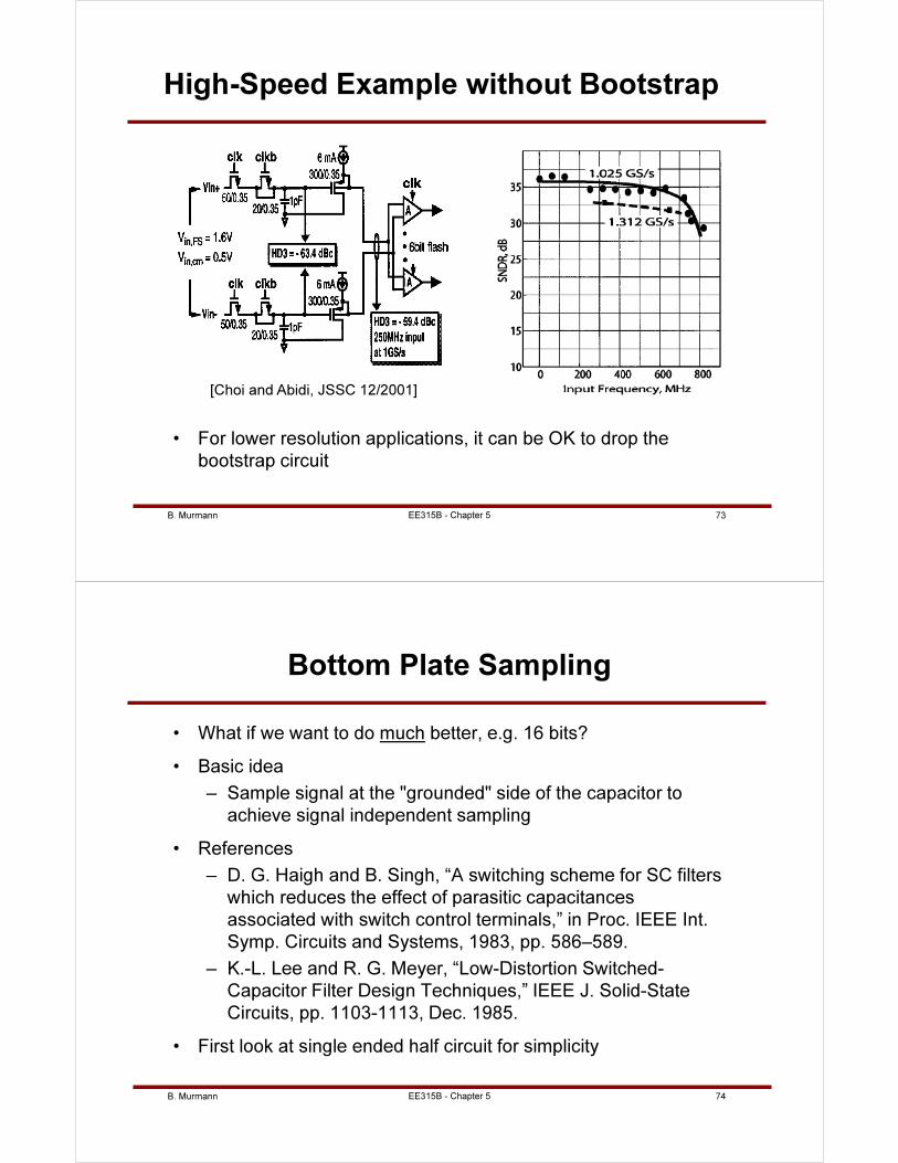
B. Murmann 73
High-Speed Example without Bootstrap
• For lower resolution applications, it can be OK to drop the
bootstrap circuit
EE315B - Chapter 5
[Choi and Abidi, JSSC 12/2001]
B. Murmann 74
Bottom Plate Sampling
• What if we want to do much better, e.g. 16 bits?
• Basic idea
– Sample signal at the "grounded" side of the capacitor to
achieve signal independent sampling
• References
– D. G. Haigh and B. Singh, “A switching scheme for SC filters
which reduces the effect of parasitic capacitances
associated with switch control terminals,” in Proc. IEEE Int.
Symp. Circuits and Systems, 1983, pp. 586–589.
– K.-L. Lee and R. G. Meyer, “Low-Distortion Switched-
Capacitor Filter Design Techniques,” IEEE J. Solid-State
Circuits, pp. 1103-1113, Dec. 1985.
• First look at single ended half circuit for simplicity
EE315B - Chapter 5
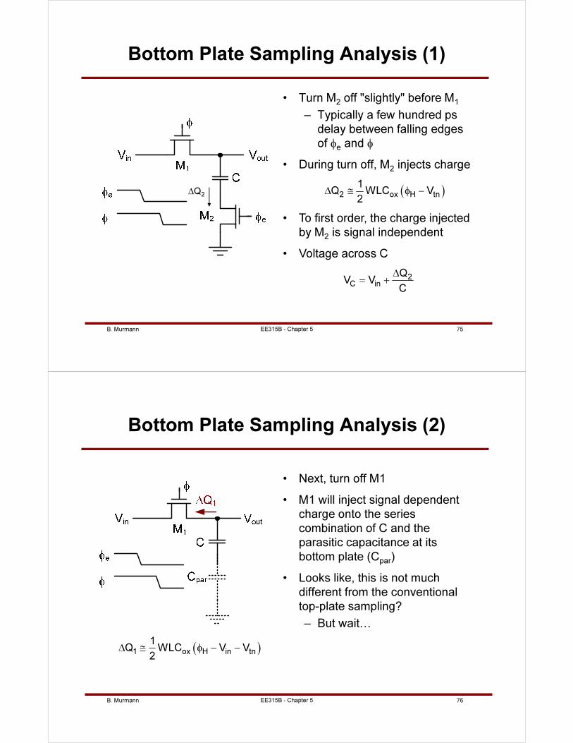
B. Murmann 75
Bottom Plate Sampling Analysis (1)
• Turn M2 off "slightly" before M1
– Typically a few hundred ps
delay between falling edges
of φe and φ
• During turn off, M2 injects charge
( )2 ox H tn
1Q WLC V
2∆ ≅ φ −
• To first order, the charge injected
by M2 is signal independent
• Voltage across C
2C in
QV V
C
∆= +
∆Q2
EE315B - Chapter 5
B. Murmann 76
Bottom Plate Sampling Analysis (2)
• Next, turn off M1
• M1 will inject signal dependent
charge onto the series
combination of C and the
parasitic capacitance at its
bottom plate (Cpar)
• Looks like, this is not much
different from the conventional
top-plate sampling?
– But wait…
EE315B - Chapter 5
( )1 ox H in tn
1Q WLC V V
2∆ ≅ φ − −
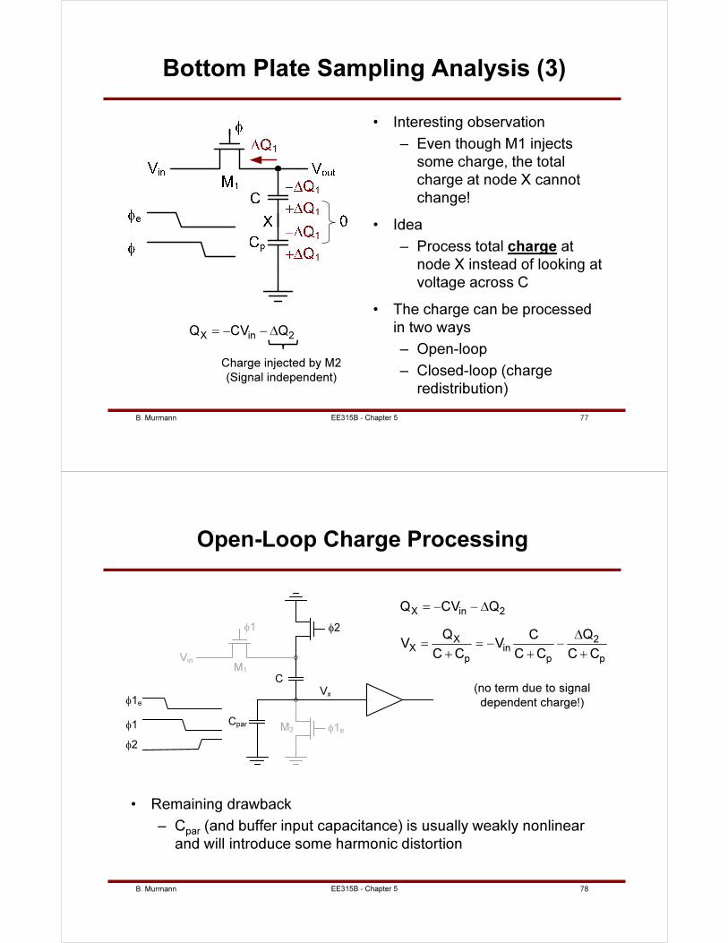
B. Murmann 77
Bottom Plate Sampling Analysis (3)
• Interesting observation
– Even though M1 injects
some charge, the total
charge at node X cannot
change!
• Idea
– Process total charge at
node X instead of looking at
voltage across C
• The charge can be processed
in two ways
– Open-loop
– Closed-loop (charge
redistribution)
EE315B - Chapter 5
X in 2Q CV Q= − − ∆
Charge injected by M2
(Signal independent)
B. Murmann 78
Open-Loop Charge Processing
• Remaining drawback
– Cpar (and buffer input capacitance) is usually weakly nonlinear
and will introduce some harmonic distortion
φ1
Vin
φ1
φ1e
M1
C
Cpar
φ2
φ1e
φ2
Vx
M2
EE315B - Chapter 5
X in 2
X 2X in
p p p
Q CV Q
Q QCV V
C C C C C C
= − − ∆
∆= = − −
+ + +
(no term due to signal
dependent charge!)
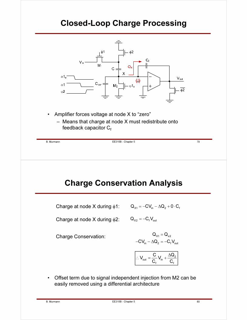
B. Murmann 79
Closed-Loop Charge Processing
• Amplifier forces voltage at node X to “zero”
– Means that charge at node X must redistribute onto
feedback capacitor Cf
EE315B - Chapter 5
B. Murmann 80
Charge Conservation Analysis
• Offset term due to signal independent injection from M2 can be
easily removed using a differential architecture
X1 in 2 fQ CV Q 0 C= − − ∆ + ⋅Charge at node X during φ1:
Charge at node X during φ2: X2 f outQ C V= −
Charge Conservation: X1 x2
in 2 f out
Q Q
CV Q C V
=
− − ∆ = −
2
out in
f f
QCV V
C C
∆∴ = +
EE315B - Chapter 5
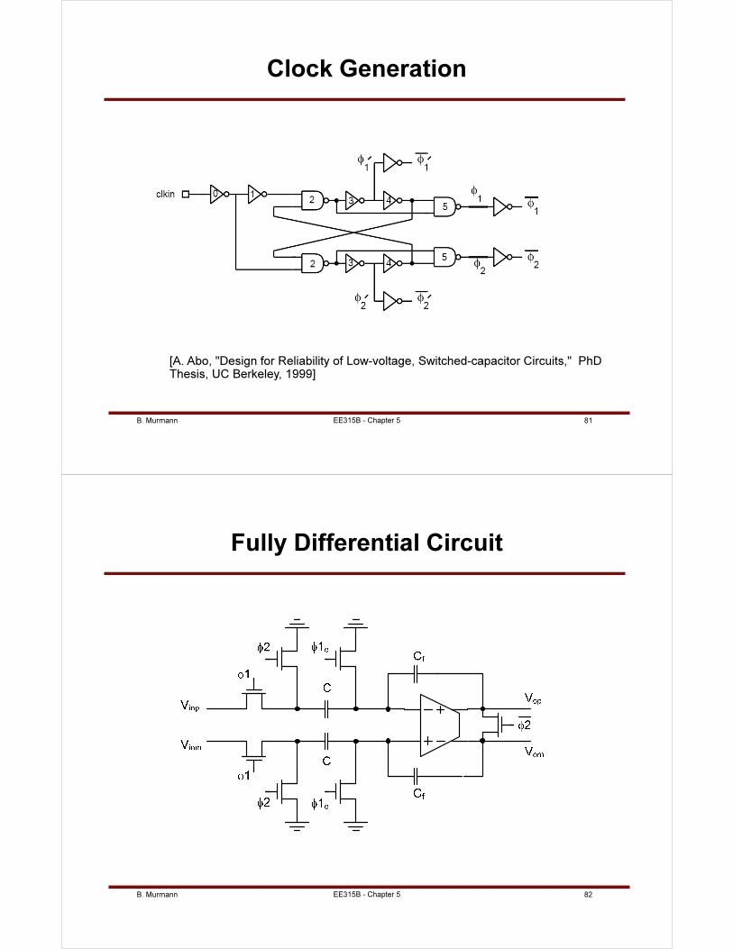
B. Murmann 81EE315B - Chapter 5
Clock Generation
[A. Abo, "Design for Reliability of Low-voltage, Switched-capacitor Circuits," PhD Thesis, UC Berkeley, 1999]
B. Murmann 82
Fully Differential Circuit
EE315B - Chapter 5
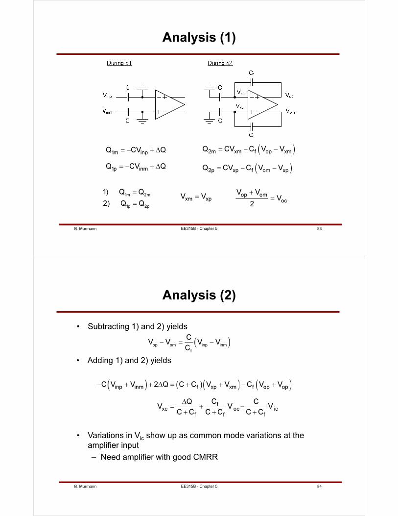
B. Murmann 83EE315B - Chapter 5
Analysis (1)
1m inp
1p inm
Q CV Q
Q CV Q
= − + ∆
= − + ∆
( )
( )
2m xm f op xm
2p xp f om xp
Q CV C V V
Q CV C V V
= − −
= − −
1m 2m
1p 2p
1) Q Q
2) Q Q
=
=
xm xpV V= op om
oc
V VV
2
+
=
B. Murmann 84EE315B - Chapter 5
Analysis (2)
• Subtracting 1) and 2) yields
( )op om inp inm
f
CV V V V
C− = −
• Adding 1) and 2) yields
( ) ( )( ) ( )inp inm f xp xm f op op
fxc oc ic
f f f
C V V 2 Q C C V V C V V
CQ CV V V
C C C C C C
− + + ∆ = + + − +
∆= + −
+ + +
• Variations in Vic show up as common mode variations at the
amplifier input
– Need amplifier with good CMRR
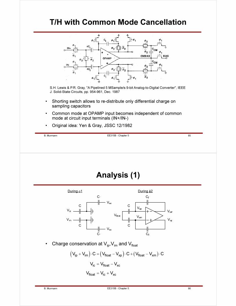
B. Murmann 85EE315B - Chapter 5
T/H with Common Mode Cancellation
• Shorting switch allows to re-distribute only differential charge on sampling capacitors
• Common mode at OPAMP input becomes independent of common mode at circuit input terminals (IN+/IN-)
• Original idea: Yen & Gray, JSSC 12/1982
S.H. Lewis & P.R. Gray, "A Pipelined 5 MSample/s 9-bit Analog-to-Digital Converter", IEEE
J. Solid-State Circuits, pp. 954-961, Dec. 1987
B. Murmann 86EE315B - Chapter 5
Analysis (1)
• Charge conservation at Vip,Vim and Vfloat
C
V
V
C
V
C
C
C
V
During 1 During 2
V
V
C
V
C
V
V
C
( ) ( ) ( )ip im float xp float xm
ic float xc
float ic xc
V V C V V C V V C
V V V
V V V
+ ⋅ = − ⋅ + − ⋅
= −
= +
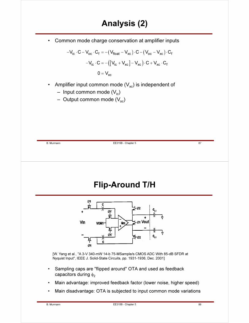
B. Murmann 87EE315B - Chapter 5
Analysis (2)
• Common mode charge conservation at amplifier inputs
( ) ( )
[ ]( )
ic oc f float xc oc xc f
ic ic xc xc xc f
xc
V C V C V V C V V C
V C V V V C V C
0 V
− ⋅ − ⋅ = − − ⋅ − − ⋅
− ⋅ = − + − ⋅ + ⋅
=
• Amplifier input common mode (Vxc) is independent of
– Input common mode (Vic)
– Output common mode (Voc)
B. Murmann 88EE315B - Chapter 5
Flip-Around T/H
• Sampling caps are "flipped around" OTA and used as feedback
capacitors during φ2
• Main advantage: improved feedback factor (lower noise, higher speed)
• Main disadvantage: OTA is subjected to input common mode variations
[W. Yang et al., "A 3-V 340-mW 14-b 75-MSample/s CMOS ADC With 85-dB SFDR at
Nyquist Input", IEEE J. Solid-State Circuits, pp. 1931-1936, Dec. 2001]
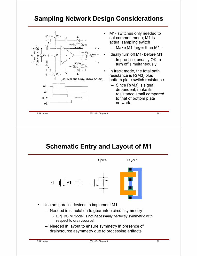
B. Murmann 89
Sampling Network Design Considerations
• M1- switches only needed to set common mode; M1 is actual sampling switch
– Make M1 larger than M1-
• Ideally turn off M1- before M1
– In practice, usually OK to turn off simultaneously
• In track mode, the total path resistance is R(M3) plus bottom plate switch resistance
– Since R(M3) is signal dependent, make its resistance small compared to that of bottom plate network
φ1-
φ1
φ1+
φ2
φ1-
φ1-
φ1φ1+
φ1+
[Lin, Kim and Gray, JSSC 4/1991]
M1-
M1-
M1
EE315B - Chapter 5
B. Murmann 90
Schematic Entry and Layout of M1
• Use antiparallel devices to implement M1
– Needed in simulation to guarantee circuit symmetry
• E.g. BSIM model is not necessarily perfectly symmetric with
respect to drain/source!
– Needed in layout to ensure symmetry in presence of
drain/source asymmetry due to processing artifacts
EE315B - Chapter 5
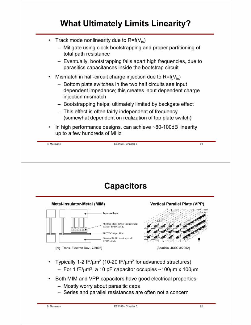
B. Murmann 91
What Ultimately Limits Linearity?
• Track mode nonlinearity due to R=f(Vin)
– Mitigate using clock bootstrapping and proper partitioning of
total path resistance
– Eventually, bootstrapping falls apart high frequencies, due to
parasitics capacitances inside the bootstrap circuit
• Mismatch in half-circuit charge injection due to R=f(Vin)
– Bottom plate switches in the two half circuits see input
dependent impedance; this creates input dependent charge
injection mismatch
– Bootstrapping helps; ultimately limited by backgate effect
– This effect is often fairly independent of frequency
(somewhat dependent on realization of top plate switch)
• In high performance designs, can achieve ~80-100dB linearity
up to a few hundreds of MHz
EE315B - Chapter 5
B. Murmann 92
Capacitors
• Typically 1-2 fF/µm2 (10-20 fF/µm2 for advanced structures)
– For 1 fF/µm2, a 10 pF capacitor occupies ~100µm x 100µm
• Both MIM and VPP capacitors have good electrical properties
– Mostly worry about parasitic caps
– Series and parallel resistances are often not a concern
EE315B - Chapter 5
[Ng, Trans. Electron Dev., 7/2005]
Metal-Insulator-Metal (MIM) Vertical Parallel Plate (VPP)
[Aparicio, JSSC 3/2002]
B. Murmann 93
Plate Parasitics
• Node n1 is usually the "physical" top plate of the capacitor
– Makes nomenclature very confusing, since this plate is
typically used as the "electrical" bottom plate in a sampling
circuit (in the context of "bottom plate sampling")
• Typical values for a MIM capacitor
– α=1%, β=10%
Ideal Capacitor
Typical Integrated
Circuit Capacitor
EE315B - Chapter 5
Symbol
B. Murmann 94
Proper Connection of Capacitors
• “Fat plate” is oriented away from virtual ground nodes to avoid
reduction of feedback factor and reduce potential noise coupling
EE315B - Chapter 5
B. Murmann 95
Outline
• Elementary track-and-hold circuit and its nonidealities
• First order improvements to elementary track-and-hold
• Advanced techniques
– Clock bootstrapping
– Bottom plate sampling
• Settling and noise analysis in charge-redistribution
track-and-hold circuit
• Noise simulation example
EE315B - Chapter 5
B. Murmann 96
Settling and Noise Analysis
Cf
CsGm
CL
φ1 φ2
EE315B - Chapter 5
B. Murmann 97
First Order Amplifier Model
x o
o od
n
2
o
x xd
( )m x m x D
o
D x
g v for g v Ii
I sign v else
<=
⋅
EE315B - Chapter 5
Piecewise linear half-circuit
B. Murmann 98
Linear Settling (Small Input Step)
• Important parameter: Return factor or "feedback factor" β
f
f s x
C
C C Cβ =
+ +
( )t /
o ofinalv (t) V 1 e− τ
= −
→Vofinalt=00
-Vistep
(ignoring feedforward zero)
EE315B - Chapter 5
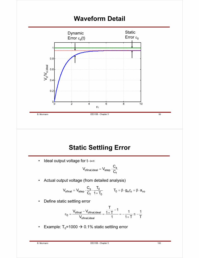
B. Murmann 99EE315B - Chapter 5
0 2 4 6 8 100
0.2
0.4
0.6
0.8
1
t/τ
Vout/Vout,ideal
Waveform Detail
Dynamic
Error εd(t)
Static
Error ε0
Vo/V
o,ideal
B. Murmann 100
Static Settling Error
• Ideal output voltage for t→∞
sofinal,ideal istep
f
CV V
C= ⋅
• Actual output voltage (from detailed analysis)
s 0ofinal istep 0 m o vo
f 0
C TV V T g r a
C 1 T= ⋅ ⋅ = β ⋅ = β ⋅
+
• Define static settling error
ofinal ofinal,ideal0
ofinal,ideal
T1
V V 1 11 T
V 1 1 T T
−−
+ε = = = − ≅ −
+
EE315B - Chapter 5
• Example: T0=1000 0.1% static settling error
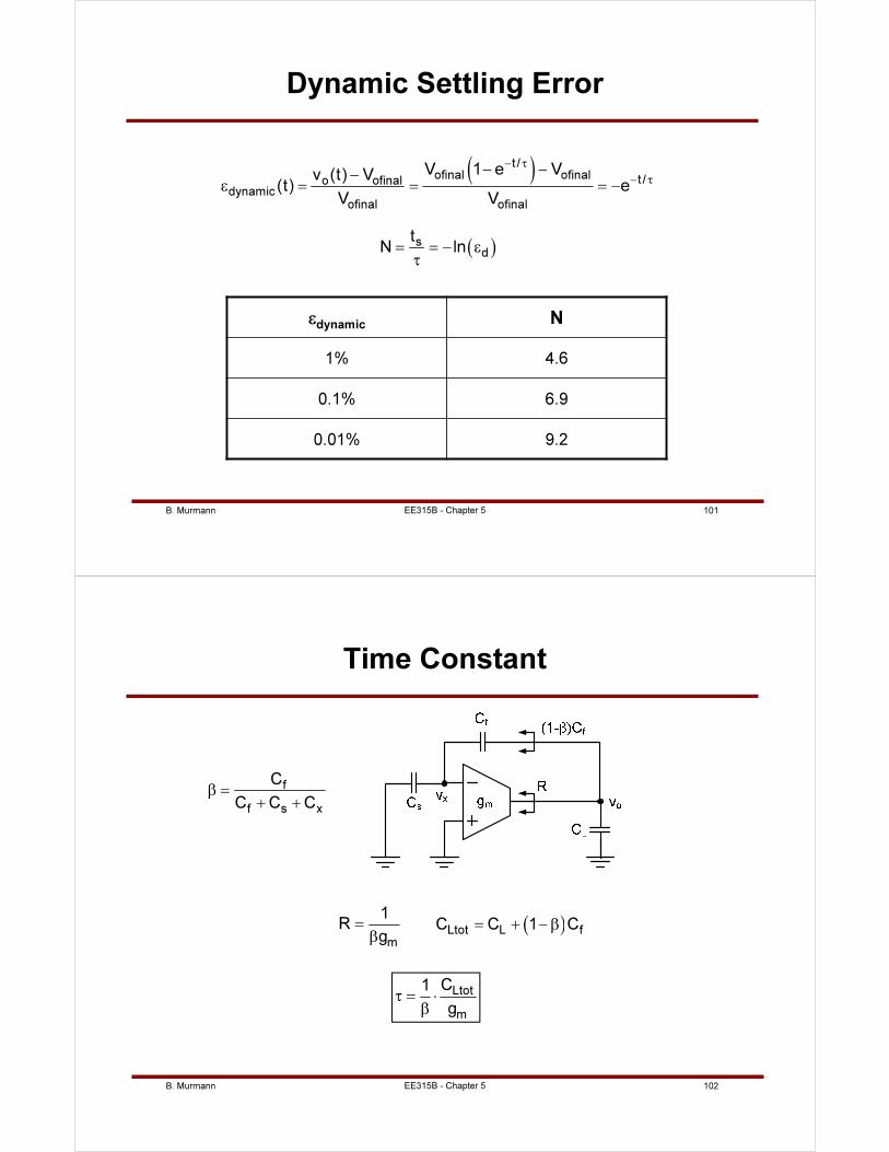
B. Murmann 101
Dynamic Settling Error
( )t /ofinal ofinal t /o ofinal
dynamicofinal ofinal
V 1 e Vv (t) V(t) e
V V
− τ
− τ
− −−
ε = = = −
( )sd
tN ln= = − ε
τ
εdynamic N
1% 4.6
0.1% 6.9
0.01% 9.2
EE315B - Chapter 5
B. Murmann 102
Time Constant
Ltot
m
C1
gτ = ⋅
β
( )Ltot L fC C 1 C= + −β
EE315B - Chapter 5
f
f s x
C
C C Cβ =
+ +
m
1R
g=β
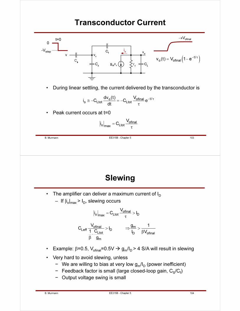
B. Murmann 103
Transconductor Current
• During linear settling, the current delivered by the transconductor is
t /o ofinalo Ltot Ltot
dv (t) Vi C C e
dt
− τ
≅ − = −
τ
( )t /
o ofinalv (t) V 1 e− τ
= −
→Vofinalt=00
-Vistep
• Peak current occurs at t=0
ofinalo Ltotmax
Vi C=
τ
EE315B - Chapter 5
B. Murmann 104
Slewing
• The amplifier can deliver a maximum current of ID
– If |io|max > ID, slewing occurs
ofinalo Ltot Dmax
Vi C I= >
τ
ofinal mLeff D
Ltot D ofinal
m
V g 1C I
C1 I V
g
> ⇒ >β
⋅β
• Example: β=0.5, Vofinal=0.5V gm/ID > 4 S/A will result in slewing
• Very hard to avoid slewing, unless
− We are willing to bias at very low gm/ID (power inefficient)
− Feedback factor is small (large closed-loop gain, CS/Cf)
− Output voltage swing is small
EE315B - Chapter 5
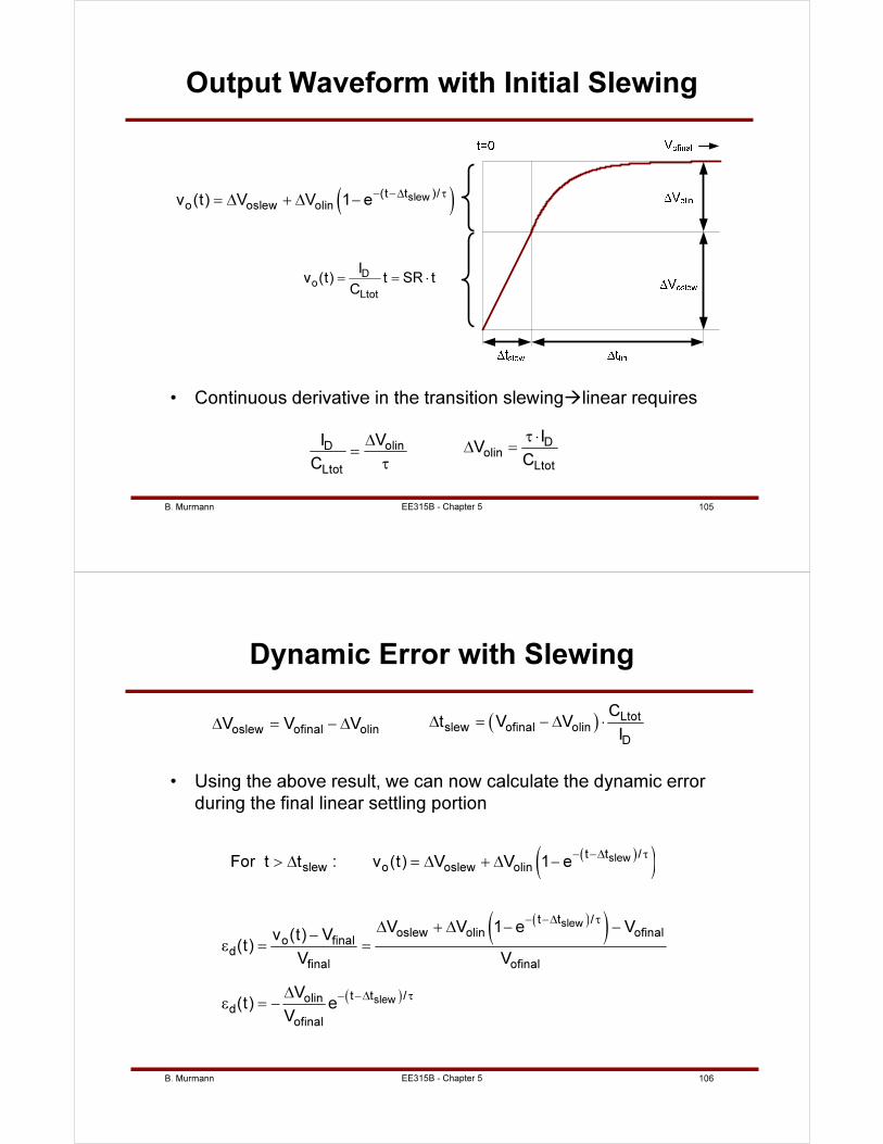
B. Murmann 105
Output Waveform with Initial Slewing
• Continuous derivative in the transition slewinglinear requires
Do
Ltot
Iv (t) t SR t
C= = ⋅
( )slew(t t )/o oslew olinv (t) V V 1 e
− −∆ τ= ∆ + ∆ −
olinD
Ltot
VI
C
∆=
τ
Dolin
Ltot
IV
C
τ ⋅∆ =
EE315B - Chapter 5
B. Murmann 106
Dynamic Error with Slewing
oslew ofinal olinV V V∆ = − ∆ ( ) Ltotslew ofinal olin
D
Ct V V
I∆ = − ∆ ⋅
• Using the above result, we can now calculate the dynamic error
during the final linear settling portion
( )( )slewt t /
slew o oslew olinFor t t : v (t) V V 1 e
− −∆ τ> ∆ = ∆ + ∆ −
( )( )
( )
slew
slew
t t /
oslew olin ofinalo final
d
final ofinal
t t /olind
ofinal
V V 1 e Vv (t) V
(t)V V
V(t) e
V
− −∆ τ
− −∆ τ
∆ + ∆ − −−
ε = =
∆ε = −
EE315B - Chapter 5
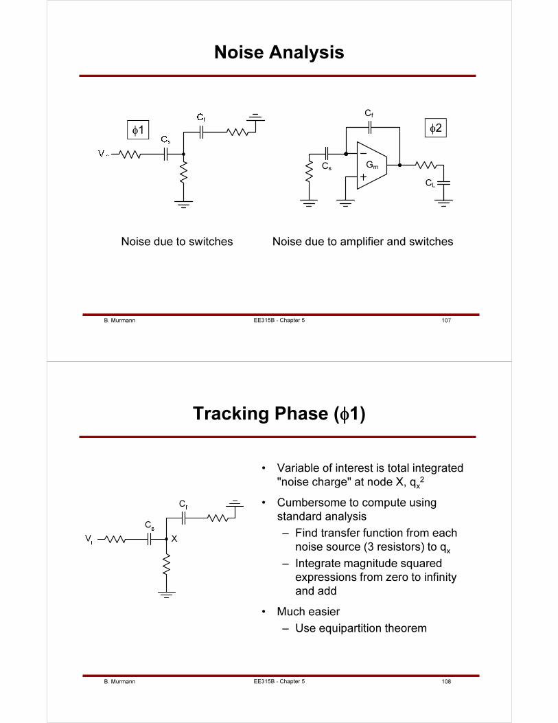
B. Murmann 107
Noise Analysis
EE315B - Chapter 5
Cf
CsGm
CL
φ1 φ2
Noise due to switches Noise due to amplifier and switches
B. Murmann 108
Tracking Phase (φ1)
V
C
C
X
• Variable of interest is total integrated
"noise charge" at node X, qx2
• Cumbersome to compute using
standard analysis
– Find transfer function from each
noise source (3 resistors) to qx
– Integrate magnitude squared
expressions from zero to infinity
and add
• Much easier
– Use equipartition theorem
EE315B - Chapter 5
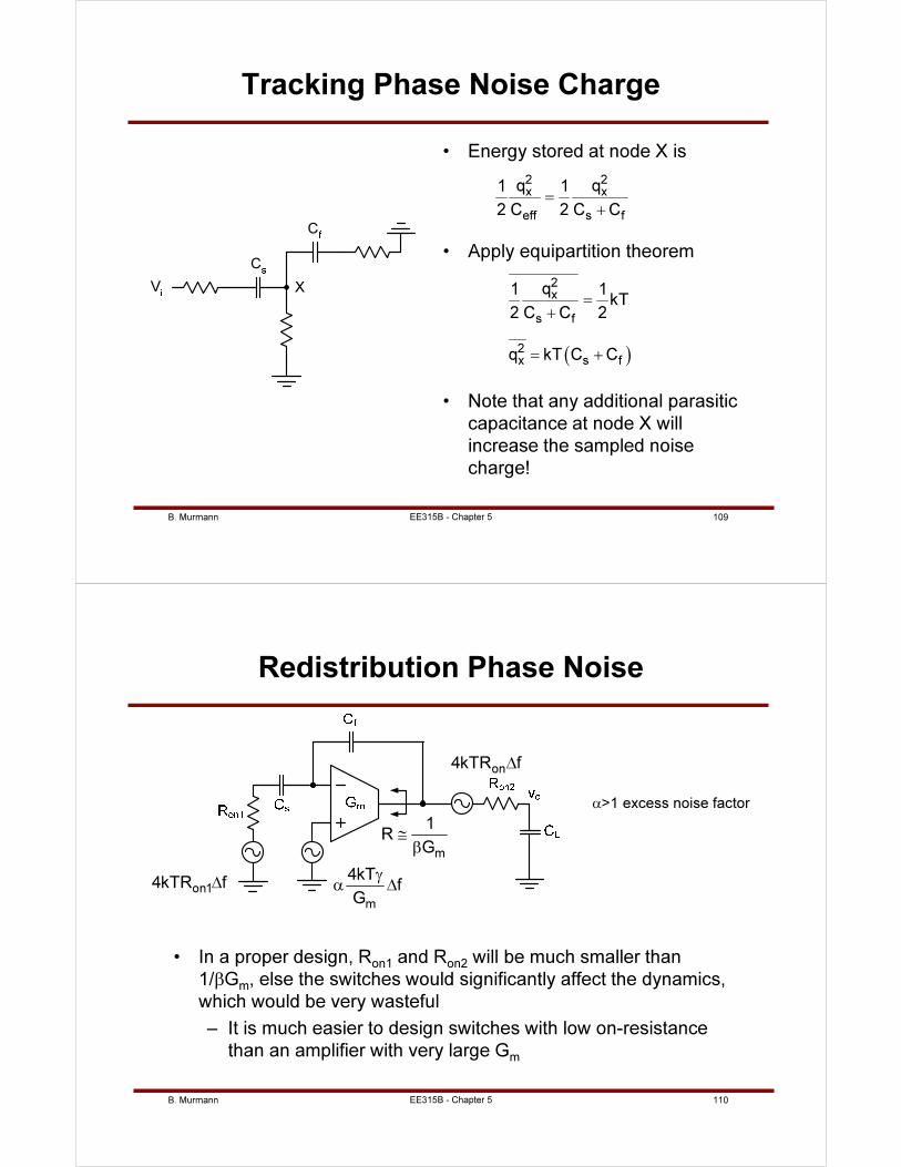
B. Murmann 109
Tracking Phase Noise Charge
V
C
C
X
• Energy stored at node X is
2 2
x x
eff s f
q q1 1
2 C 2 C C=
+
• Apply equipartition theorem
( )
2
x
s f
2
x s f
q1 1kT
2 C C 2
q kT C C
=
+
= +
• Note that any additional parasitic
capacitance at node X will
increase the sampled noise
charge!
EE315B - Chapter 5
B. Murmann 110
Redistribution Phase Noise
• In a proper design, Ron1 and Ron2 will be much smaller than
1/βGm, else the switches would significantly affect the dynamics,
which would be very wasteful
– It is much easier to design switches with low on-resistance
than an amplifier with very large Gm
EE315B - Chapter 5
on14kTR f∆
on4kTR f∆
m
4kTf
G
γα ∆
α>1 excess noise factor
m
1R
G≅β
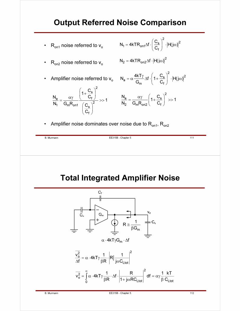
B. Murmann 111
Output Referred Noise Comparison
• Ron1 noise referred to vo
EE315B - Chapter 5
2
2s1 on1
f
CN 4kTR f H( j )
C
= ∆ ⋅ ⋅ ω
2
2sa
m f
C4kTN f 1 H( j )
G C
γ= α ∆ ⋅ + ⋅ ω
2
s
fa
21 m on1
s
f
C1
CN1
N G RC
C
+
αγ = >>
• Amplifier noise referred to vo
• Ron2 noise referred to vo
2
2 on2N 4kTR f H( j )= ∆ ⋅ ω
2
a s
2 m on2 f
N C1 1
N G R C
αγ= + >>
• Amplifier noise dominates over noise due to Ron1, Ron2
B. Murmann 112
Total Integrated Amplifier Noise
EE315B - Chapter 5
m4kT G fα ⋅ γ ⋅ ∆
m
1R
G≅β
22
o
Ltot
2
2
o
Ltot Ltot0
v 1 14kT R
f R j C
1 R 1 kTv 4kT f df
R 1 j RC C
∞
= α ⋅ γ ⋅∆ β ω
= α ⋅ γ ⋅ ∆ ⋅ = αγβ + ω β∫
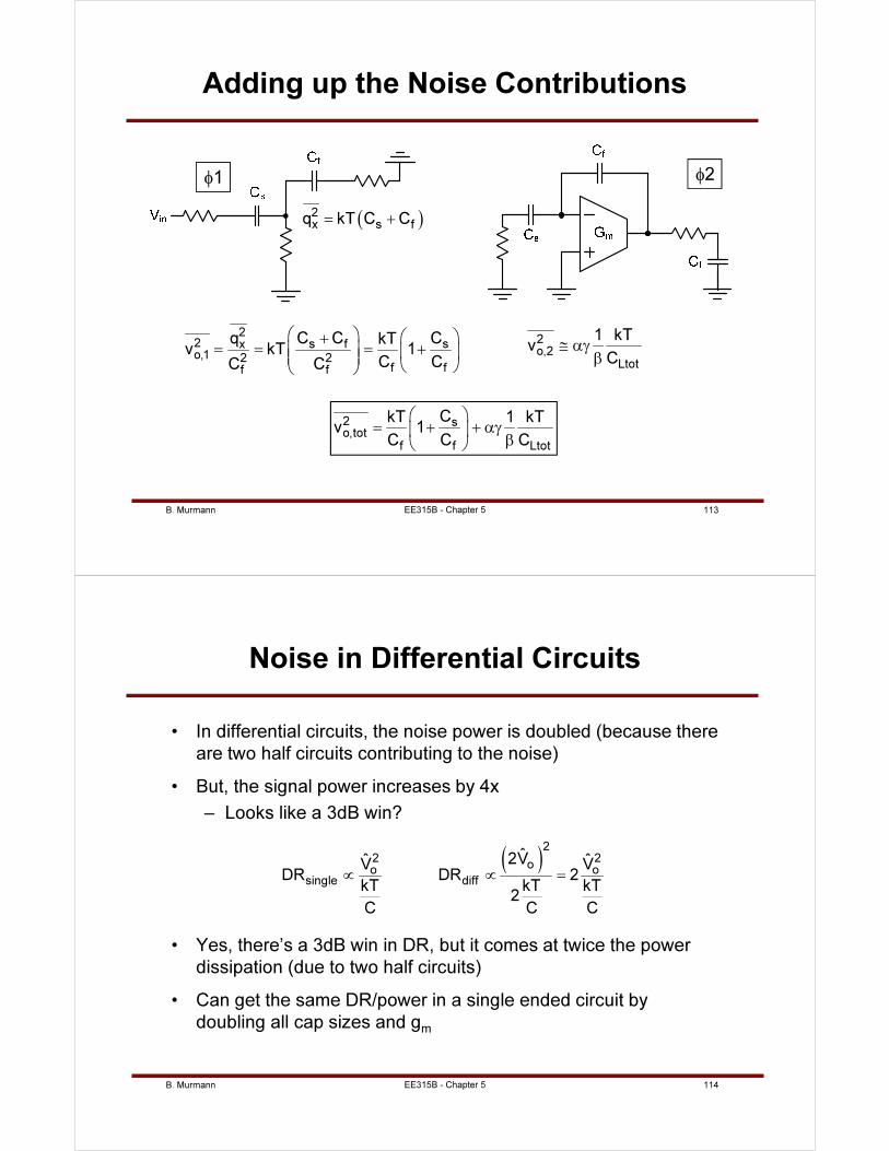
B. Murmann 113
Adding up the Noise Contributions
EE315B - Chapter 5
φ1 φ2
( )2
x s fq kT C C= +
22 s f sxo,1 2 2
f ff f
C C Cq kTv kT 1
C CC C
+= = = +
2o,2
Ltot
1 kTv
C≅ αγ
β
2 so,tot
f f Ltot
CkT 1 kTv 1
C C C
= + + αγ
β
B. Murmann 114EE315B - Chapter 5
Noise in Differential Circuits
• In differential circuits, the noise power is doubled (because there
are two half circuits contributing to the noise)
• But, the signal power increases by 4x
– Looks like a 3dB win?
( )2
2 2oo o
single diff
ˆ2Vˆ ˆV VDR DR 2
kT kT kT2
C C C
∝ ∝ =
• Yes, there’s a 3dB win in DR, but it comes at twice the power
dissipation (due to two half circuits)
• Can get the same DR/power in a single ended circuit by
doubling all cap sizes and gm
B. Murmann 115
Outline
• Elementary track-and-hold circuit and its nonidealities
• First order improvements to elementary track-and-hold
• Advanced techniques
– Clock bootstrapping
– Bottom plate sampling
• Settling and noise analysis in charge-redistribution
track-and-hold circuit
• Noise simulation example
EE315B - Chapter 5
B. Murmann 116
SC Noise Simulation
• There are at least three ways to simulate noise in switched
capacitor circuits
• Basic .ac/.noise Spice simulations
– Simulate noise in each clock phase separately
• Activate φ1 switches, run .noise and integrate noise
charge at relevant node over all frequencies and refer to
output
• Activate φ2 switches, run .noise and integrate noise over
all frequencies at the output
• Sum integrated noise from the two phases
– This is analogous to the way we carried out the hand
analysis
EE315B - Chapter 5
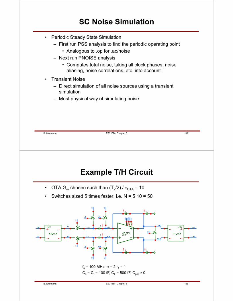
B. Murmann 117
SC Noise Simulation
• Periodic Steady State Simulation
– First run PSS analysis to find the periodic operating point
• Analogous to .op for .ac/noise
– Next run PNOISE analysis
• Computes total noise, taking all clock phases, noise
aliasing, noise correlations, etc. into account
• Transient Noise
– Direct simulation of all noise sources using a transient
simulation
– Most physical way of simulating noise
EE315B - Chapter 5
B. Murmann 118
Example T/H Circuit
• OTA Gm chosen such than (Ts/2) / τOTA = 10
• Switches sized 5 times faster, i.e. N = 5∙10 = 50
voc
vdd
p1
vocs
p1
vic
vic
vic
vic
cs
Csp
cf
Cfp
cl
Clp
cf
Cfm
cl
Clm
cs
Csm
fs = 100 MHz, α = 2, γ = 1
Cs = Cf = 100 fF, CL = 500 fF, Cpar ≅ 0
EE315B - Chapter 5
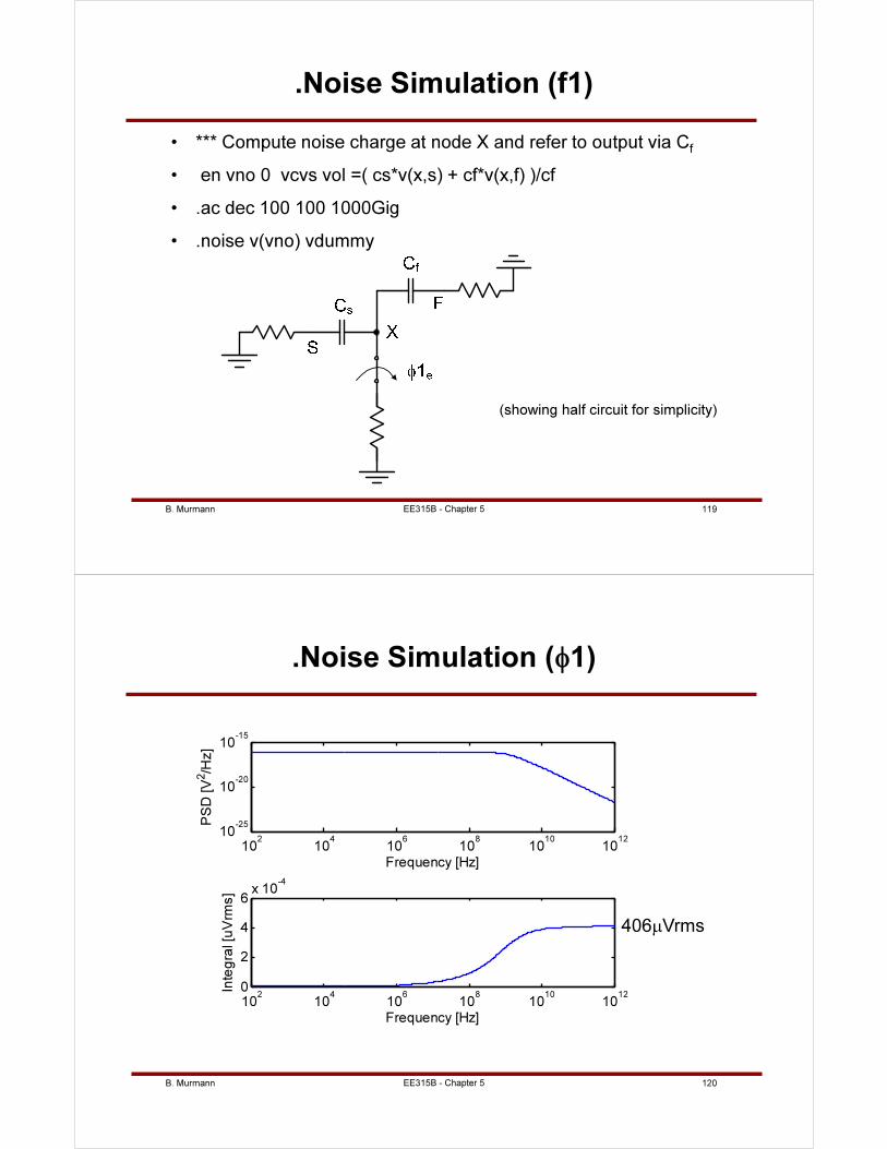
B. Murmann 119
.Noise Simulation (f1)
• *** Compute noise charge at node X and refer to output via Cf
• en vno 0 vcvs vol =( cs*v(x,s) + cf*v(x,f) )/cf
• .ac dec 100 100 1000Gig
• .noise v(vno) vdummy
(showing half circuit for simplicity)
EE315B - Chapter 5
B. Murmann 120
102
104
106
108
1010
1012
10-25
10-20
10-15
PS
D [V2/H
z]
Frequency [Hz]
102
104
106
108
1010
1012
0
2
4
6x 10
-4
Inte
gra
l [u
Vrm
s]
Frequency [Hz]
.Noise Simulation (φ1)
406µVrms
EE315B - Chapter 5
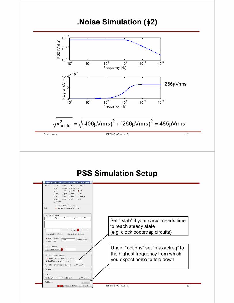
B. Murmann 121
102
104
106
108
1010
1012
10-25
10-20
10-15
PS
D [V2/H
z]
Frequency [Hz]
102
104
106
108
1010
1012
0
2
4x 10
-4
Inte
gra
l [u
Vrm
s]
Frequency [Hz]
.Noise Simulation (φ2)
( ) ( )2 22
out,totv 406 Vrms 266 Vrms 485 Vrms= µ + µ = µ
266µVrms
EE315B - Chapter 5
B. Murmann 122
PSS Simulation Setup
Under “options” set “maxacfreq” to
the highest frequency from which
you expect noise to fold down
Set “tstab” if your circuit needs time
to reach steady state
(e.g. clock bootstrap circuits)
EE315B - Chapter 5
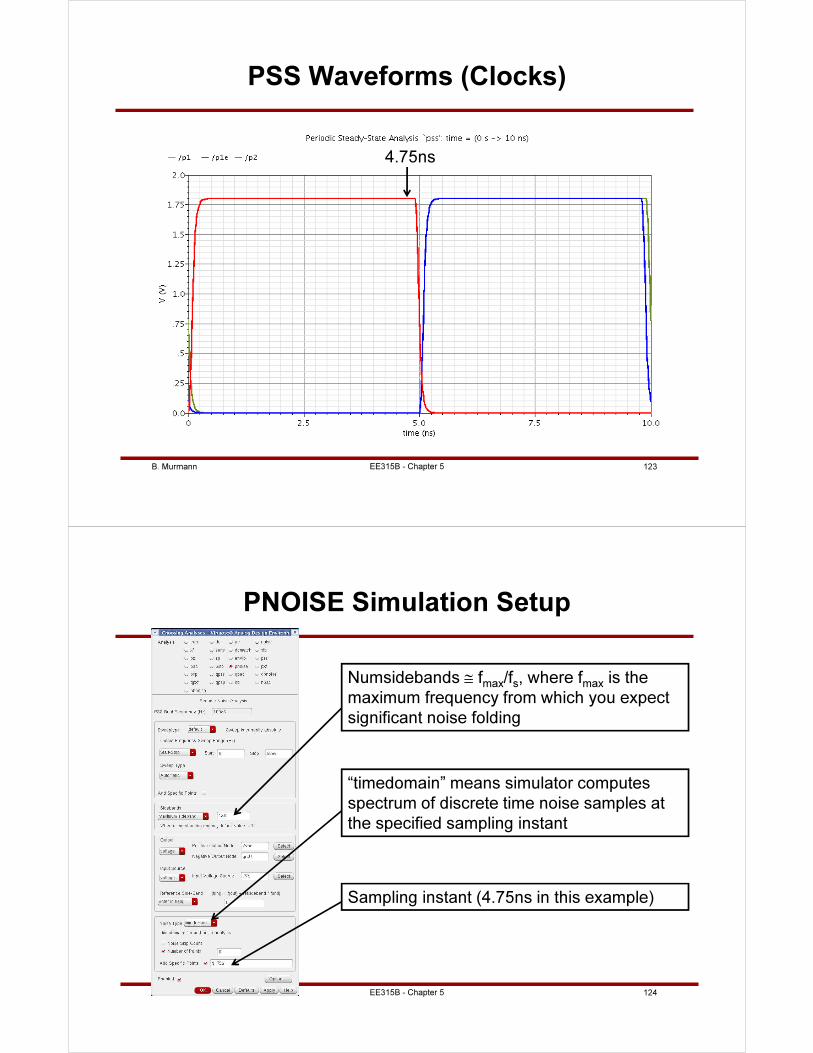
B. Murmann 123
PSS Waveforms (Clocks)
4.75ns
EE315B - Chapter 5
B. Murmann 124
PNOISE Simulation Setup
Numsidebands ≅ fmax/fs, where fmax is the
maximum frequency from which you expect
significant noise folding
“timedomain” means simulator computes
spectrum of discrete time noise samples at
the specified sampling instant
Sampling instant (4.75ns in this example)
EE315B - Chapter 5

B. Murmann 125
How to Chose Parameters
• Maxacfreq must be set commensurate with the speed
of the switches
– Common pitfall: Use nice 1mΩ switches must
consider noise from “DC to daylight”
• In our example
s
on
1 10Maxacfreq 10 N f
2 R C
Maxacfreq 3 50 100MHz 15GHz
≅ ⋅ = ⋅ ⋅
π π
≅ ⋅ ⋅ =
EE315B - Chapter 5
B. Murmann 126
How to Chose Parameters
• In traditional PSS/PNOISE simulators (such as
SpectreRF), simulation time increases rapidly for large
values of Numsidebands
• Berkeley Design Automation (BDA) Analog FastSPICE
(AFS) automatically includes an infinite number of
sidebands at significantly reduced simulation times
s
Maxacfreq 15GHzNumsidebands 150
f 100MHz≅ = =
EE315B - Chapter 5
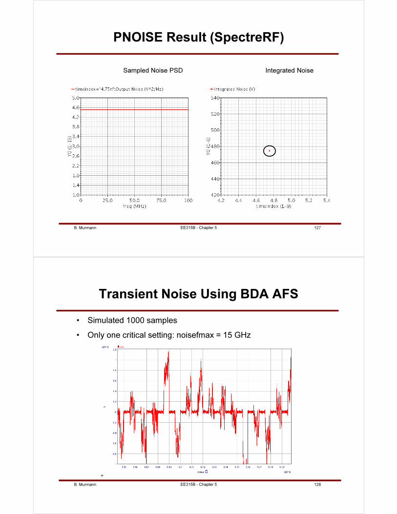
B. Murmann 127
PNOISE Result (SpectreRF)
Integrated NoiseSampled Noise PSD
EE315B - Chapter 5
B. Murmann 128
Transient Noise Using BDA AFS
• Simulated 1000 samples
• Only one critical setting: noisefmax = 15 GHz
EE315B - Chapter 5
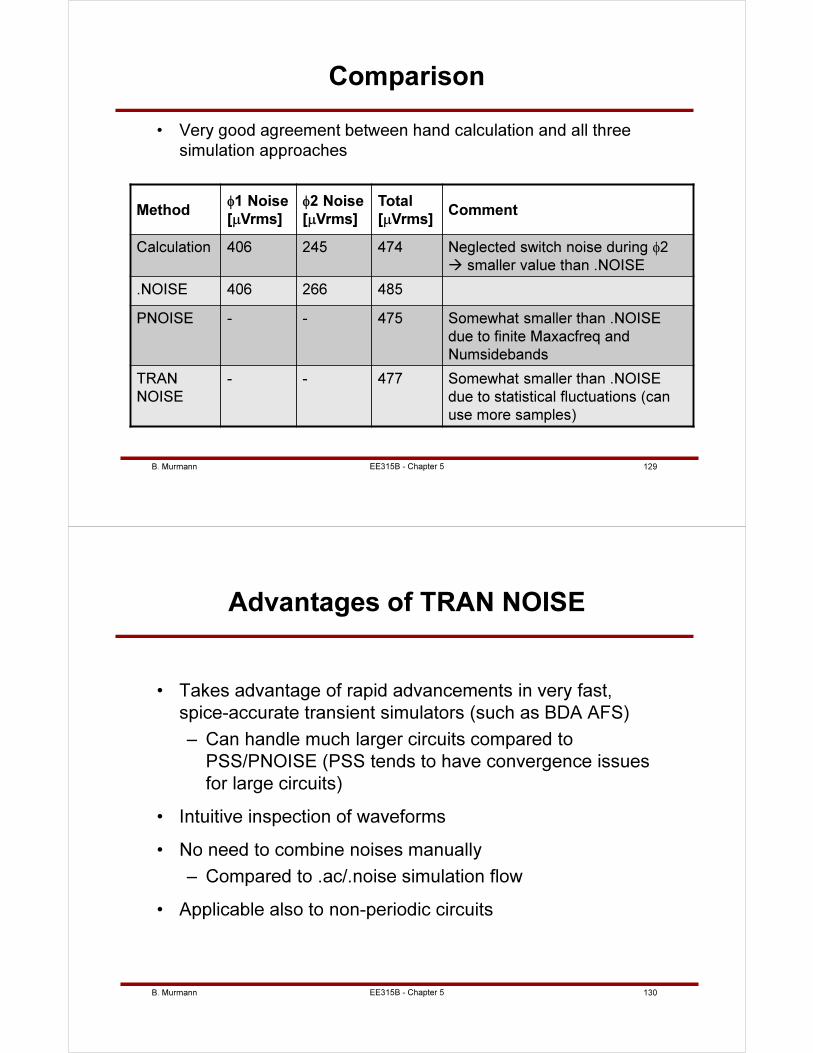
B. Murmann 129
Comparison
• Very good agreement between hand calculation and all three
simulation approaches
Methodφ1 Noise
[µVrms]
φ2 Noise
[µVrms]
Total
[µVrms]Comment
Calculation 406 245 474 Neglected switch noise during φ2
smaller value than .NOISE
.NOISE 406 266 485
PNOISE - - 475 Somewhat smaller than .NOISE
due to finite Maxacfreq and
Numsidebands
TRAN
NOISE
- - 477 Somewhat smaller than .NOISE
due to statistical fluctuations (can
use more samples)
EE315B - Chapter 5
B. Murmann 130
Advantages of TRAN NOISE
• Takes advantage of rapid advancements in very fast,
spice-accurate transient simulators (such as BDA AFS)
– Can handle much larger circuits compared to
PSS/PNOISE (PSS tends to have convergence issues
for large circuits)
• Intuitive inspection of waveforms
• No need to combine noises manually
– Compared to .ac/.noise simulation flow
• Applicable also to non-periodic circuits
EE315B - Chapter 5
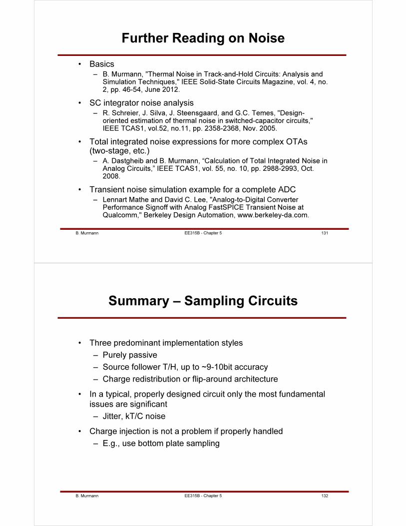
B. Murmann 131
Further Reading on Noise
• Basics– B. Murmann, "Thermal Noise in Track-and-Hold Circuits: Analysis and
Simulation Techniques," IEEE Solid-State Circuits Magazine, vol. 4, no. 2, pp. 46-54, June 2012.
• SC integrator noise analysis– R. Schreier, J. Silva, J. Steensgaard, and G.C. Temes, "Design-
oriented estimation of thermal noise in switched-capacitor circuits," IEEE TCAS1, vol.52, no.11, pp. 2358-2368, Nov. 2005.
• Total integrated noise expressions for more complex OTAs (two-stage, etc.)– A. Dastgheib and B. Murmann, “Calculation of Total Integrated Noise in
Analog Circuits,” IEEE TCAS1, vol. 55, no. 10, pp. 2988-2993, Oct. 2008.
• Transient noise simulation example for a complete ADC– Lennart Mathe and David C. Lee, "Analog-to-Digital Converter
Performance Signoff with Analog FastSPICE Transient Noise at Qualcomm," Berkeley Design Automation, www.berkeley-da.com.
EE315B - Chapter 5
B. Murmann 132
Summary – Sampling Circuits
• Three predominant implementation styles
– Purely passive
– Source follower T/H, up to ~9-10bit accuracy
– Charge redistribution or flip-around architecture
• In a typical, properly designed circuit only the most fundamental
issues are significant
– Jitter, kT/C noise
• Charge injection is not a problem if properly handled
– E.g., use bottom plate sampling
EE315B - Chapter 5
B. Murmann 1EE315B - Chapter 6
Voltage Comparators
Boris Murmann
Stanford University
Copyright © 2013 by Boris Murmann
B. Murmann 2EE315B - Chapter 6
Recap
• Ultimately, building a quantizer requires circuit elements that
"make decisions"
• The most widely used "decision circuit" is a voltage comparator
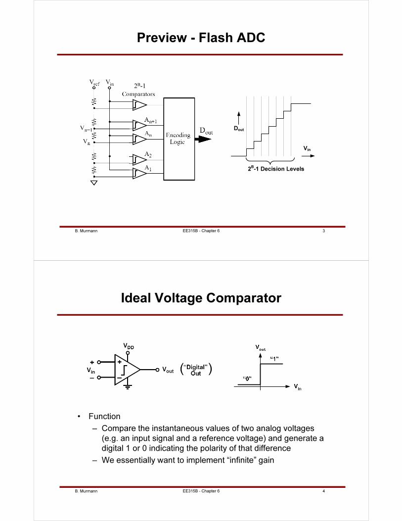
B. Murmann 3EE315B - Chapter 6
Preview - Flash ADC
Dout
Vin
2B-1 Decision Levels
2B-1
B. Murmann 4EE315B - Chapter 6
Ideal Voltage Comparator
• Function
– Compare the instantaneous values of two analog voltages
(e.g. an input signal and a reference voltage) and generate a
digital 1 or 0 indicating the polarity of that difference
– We essentially want to implement “infinite” gain
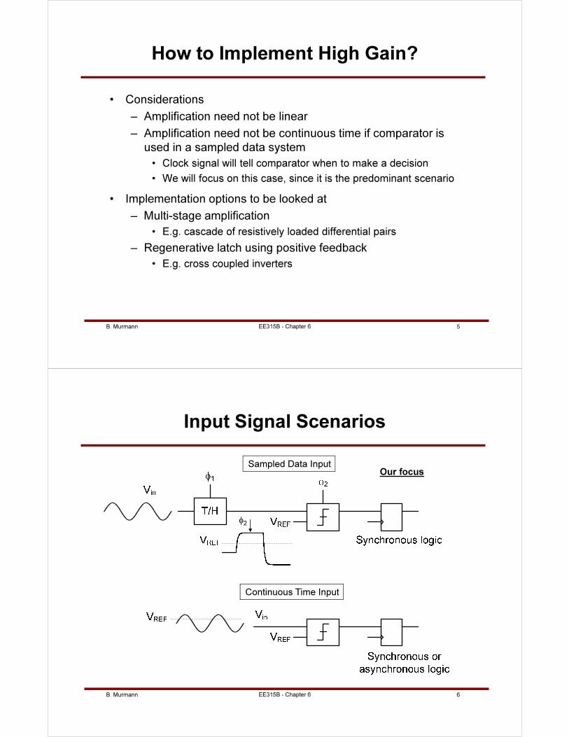
B. Murmann 5EE315B - Chapter 6
How to Implement High Gain?
• Considerations
– Amplification need not be linear
– Amplification need not be continuous time if comparator is
used in a sampled data system
• Clock signal will tell comparator when to make a decision
• We will focus on this case, since it is the predominant scenario
• Implementation options to be looked at
– Multi-stage amplification
• E.g. cascade of resistively loaded differential pairs
– Regenerative latch using positive feedback
• E.g. cross coupled inverters
B. Murmann 6
Input Signal Scenarios
EE315B - Chapter 6
Sampled Data Input
Continuous Time Input
Our focus
φ2
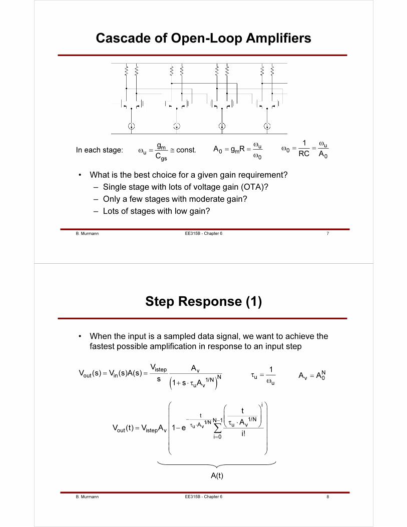
B. Murmann 7EE315B - Chapter 6
Cascade of Open-Loop Amplifiers
• What is the best choice for a given gain requirement?
– Single stage with lots of voltage gain (OTA)?
– Only a few stages with moderate gain?
– Lots of stages with low gain?
mu
gs
gconst.
Cω = ≅In each stage:
u0 m
0
A g Rω
= =
ω
u0
0
1
RC A
ω
ω = =
B. Murmann 8EE315B - Chapter 6
Step Response (1)
• When the input is a sampled data signal, we want to achieve the
fastest possible amplification in response to an input step
( )istep v
out in N1/N
u v
V AV (s) V (s)A(s)
s1 s A
= =
+ ⋅ τ
1/Nu v
i
t1/NN 1
A u vout istep v
i 0
t
AV (t) V A 1 e
i!
− −
τ ⋅
=
τ ⋅ = −
∑
u
u
1τ =
ω
N
v 0A A=
A(t)
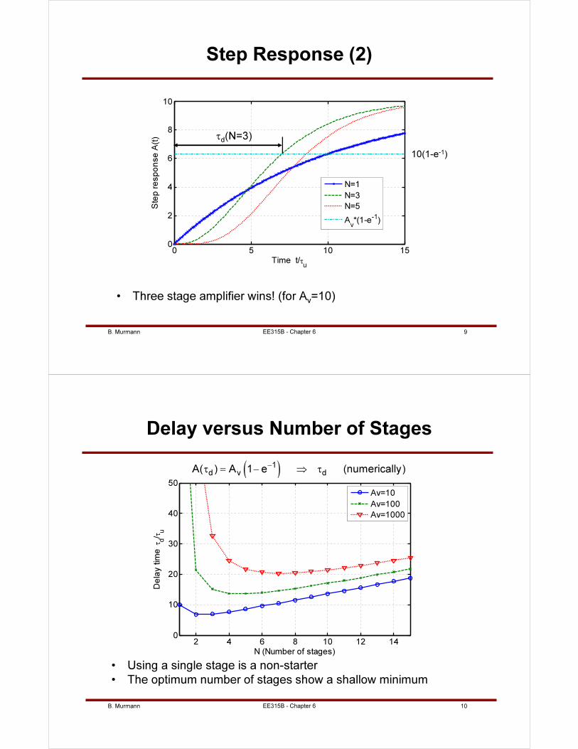
B. Murmann 9EE315B - Chapter 6
0 5 10 150
2
4
6
8
10
Time t/τu
Ste
p r
esp
on
se
A(t
)
N=1
N=3
N=5
Av*(1-e-1)
Step Response (2)
• Three stage amplifier wins! (for Av=10)
τd(N=3)
10(1-e-1)
B. Murmann 10EE315B - Chapter 6
Delay versus Number of Stages
• Using a single stage is a non-starter
• The optimum number of stages show a shallow minimum
( )1d v dA( ) A 1 e (numerically)−
τ = − ⇒ τ
2 4 6 8 10 12 140
10
20
30
40
50
N (Number of stages)
De
lay tim
e τ
d/ τu
Av=10
Av=100
Av=1000
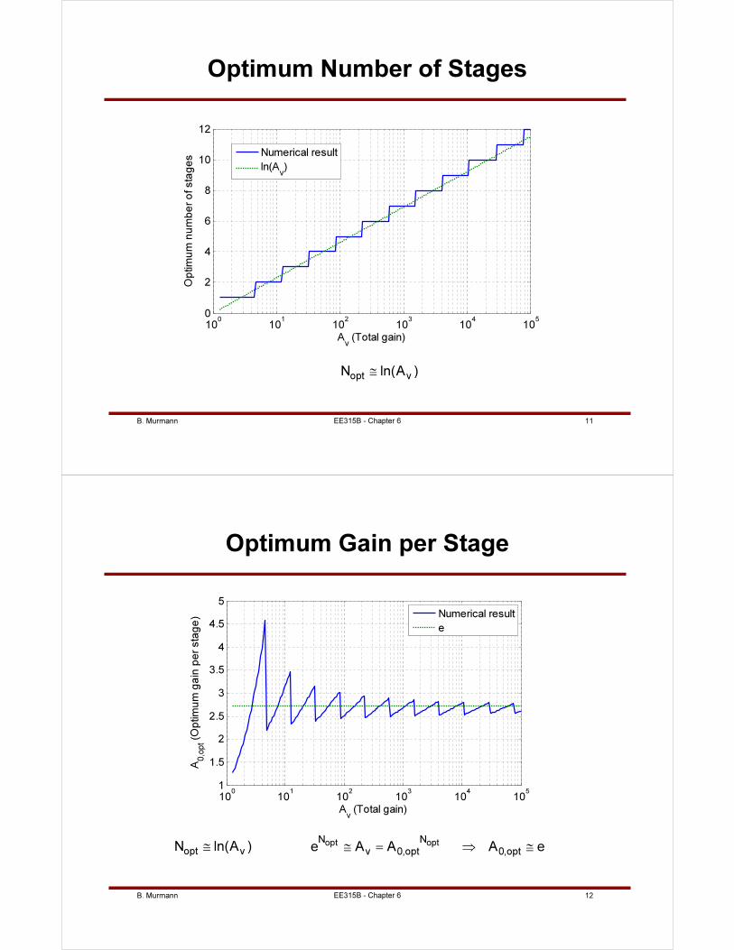
B. Murmann 11EE315B - Chapter 6
Optimum Number of Stages
opt vN ln(A )≅
100
101
102
103
104
105
0
2
4
6
8
10
12
Av (Total gain)
Op
tim
um
nu
mb
er
of sta
ge
s
Numerical result
ln(Av)
B. Murmann 12EE315B - Chapter 6
Optimum Gain per Stage
opt vN ln(A )≅opt optN N
v 0,opt 0,opte A A A e≅ = ⇒ ≅
100
101
102
103
104
105
1
1.5
2
2.5
3
3.5
4
4.5
5
Av (Total gain)
A0,opt (
Op
tim
um
ga
in p
er
sta
ge
)
Numerical result
e
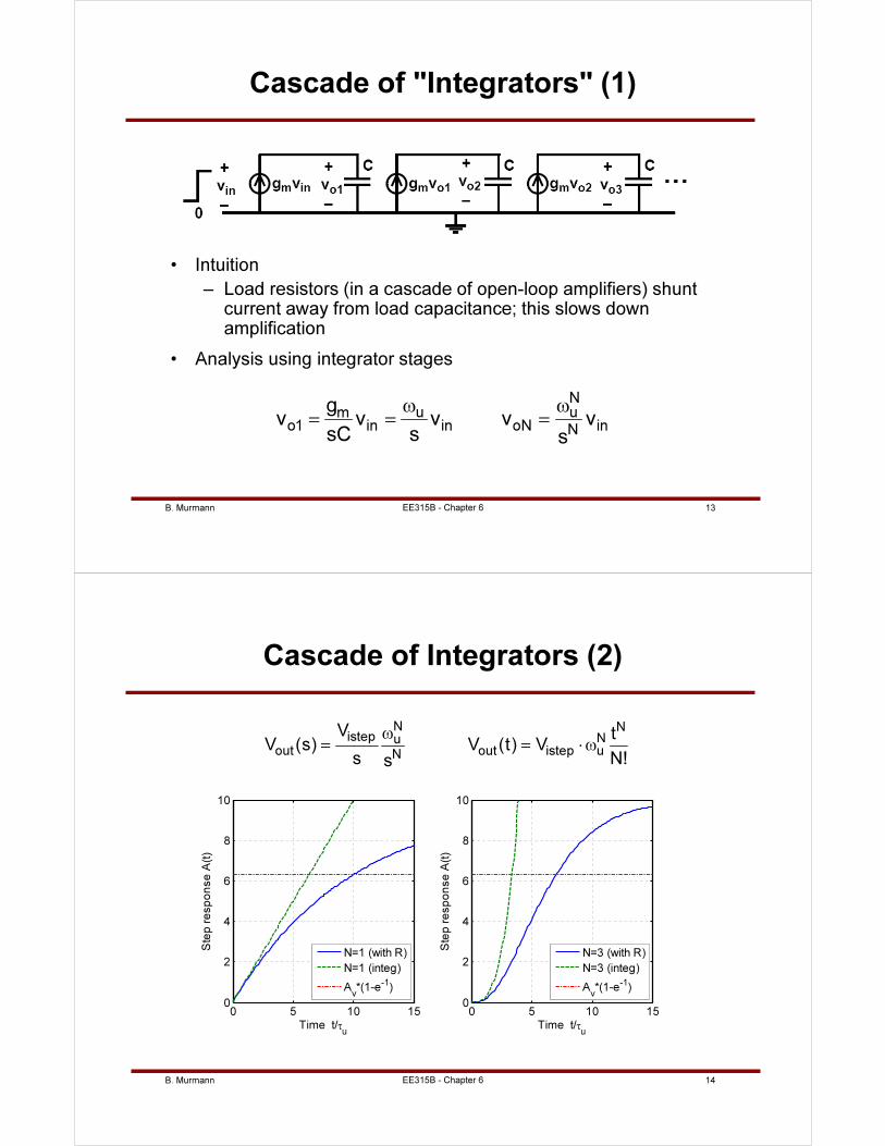
B. Murmann 13EE315B - Chapter 6
Cascade of "Integrators" (1)
• Intuition
– Load resistors (in a cascade of open-loop amplifiers) shunt current away from load capacitance; this slows down amplification
• Analysis using integrator stages
N
u umo1 in in oN inN
gv v v v v
sC s s
ω ω
= = =
B. Murmann 14EE315B - Chapter 6
Cascade of Integrators (2)
N Nistep Nu
out out istep uN
V tV (s) V (t) V
s N!s
ω
= = ⋅ω
0 5 10 150
2
4
6
8
10
Time t/τu
Ste
p r
esp
on
se
A(t
)
N=1 (with R)
N=1 (integ)
Av*(1-e
-1)
0 5 10 150
2
4
6
8
10
Time t/τu
Ste
p r
esp
on
se
A(t
)
N=3 (with R)
N=3 (integ)
Av*(1-e
-1)
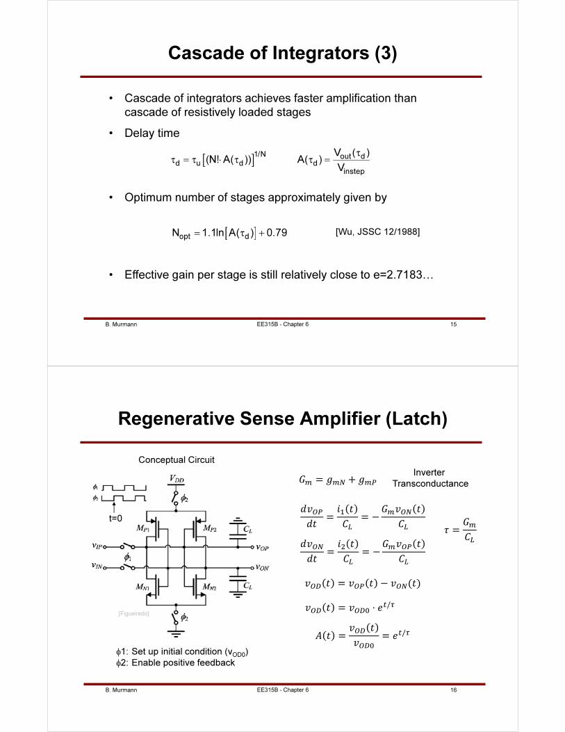
B. Murmann 15EE315B - Chapter 6
Cascade of Integrators (3)
• Cascade of integrators achieves faster amplification than
cascade of resistively loaded stages
• Delay time
[ ]1/N out d
d u d dinstep
V ( )(N! A( )) A( )
V
τ
τ = τ ⋅ τ τ =
• Optimum number of stages approximately given by
[ ]opt dN 1.1ln A( ) 0.79= τ + [Wu, JSSC 12/1988]
• Effective gain per stage is still relatively close to e=2.7183…
B. Murmann 16EE315B - Chapter 6
Regenerative Sense Amplifier (Latch)
Conceptual Circuit
φ1: Set up initial condition (vOD0)
φ2: Enable positive feedback
Inverter
Transconductance
t=0
⋅ /
/
[Figueiredo]
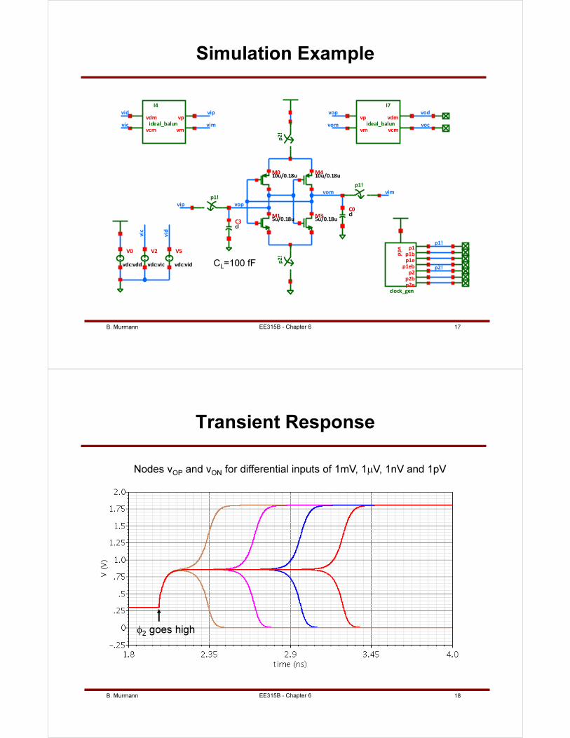
B. Murmann 17
Simulation Example
EE315B - Chapter 6
vid
vop
vom
p2!
vod vip
vim vic
vid
p1!
vic
voc
vop
vim vom
vip
V5
vdc:vid
V2
vdc:vic
V0
vdc:vdd
vm
vp
vcm
vdm
I4
ideal_balun vm
vp
vcm
vdm
I7
ideal_balun
p2
! p
2!
10u/0.18u M4
10u/0.18u M0
M3 5u/0.18u
M1 5u/0.18u
cl C0
cl C3
p1!
p1!
vd
d
clock_gen p2e p2b
p2 p1eb
p1e p1b
p1
CL=100 fF
B. Murmann 18
Transient Response
EE315B - Chapter 6
Nodes vOP and vON for differential inputs of 1mV, 1µV, 1nV and 1pV
φ2 goes high
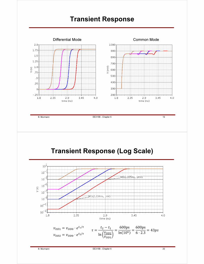
B. Murmann 19
Transient Response
EE315B - Chapter 6
Differential Mode Common Mode
B. Murmann 20
Transient Response (Log Scale)
EE315B - Chapter 6
= ⋅ /
= ⋅ /
= −
ln
=600ps
ln 10 =
600ps
6 ⋅ 2.3= 43
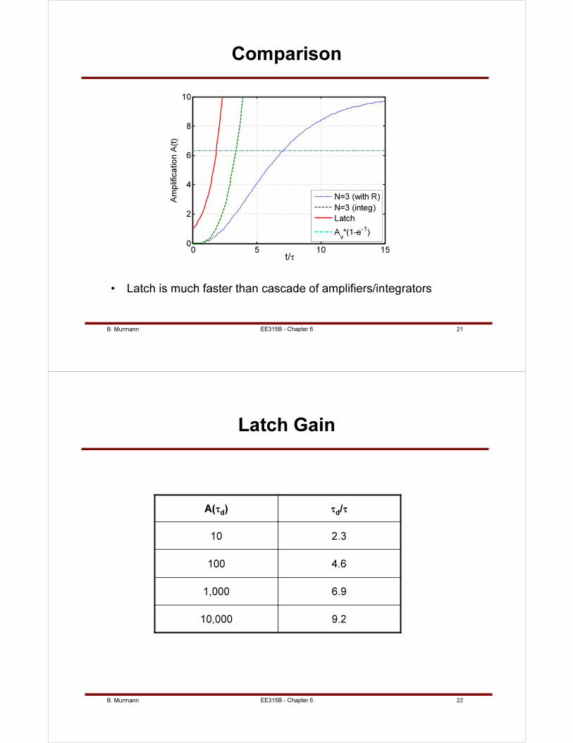
B. Murmann 21EE315B - Chapter 6
Comparison
• Latch is much faster than cascade of amplifiers/integrators
0 5 10 150
2
4
6
8
10
Time t/τ
Am
plif
ica
tio
n A
(t)
N=3 (with R)
N=3 (integ)
Latch
Av*(1-e-1)
t/τ
B. Murmann 22EE315B - Chapter 6
Latch Gain
A(τd) τ
d/τ
10 2.3
100 4.6
1,000 6.9
10,000 9.2
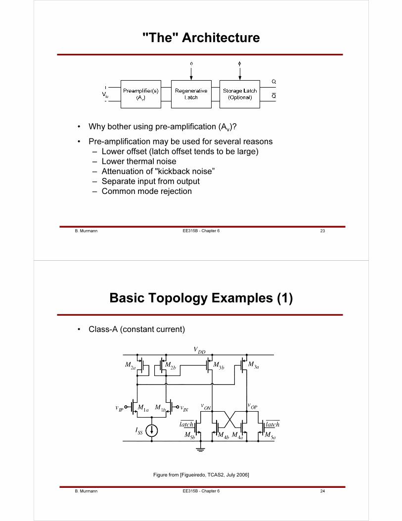
B. Murmann 23EE315B - Chapter 6
"The" Architecture
• Why bother using pre-amplification (Av)?
• Pre-amplification may be used for several reasons
– Lower offset (latch offset tends to be large)
– Lower thermal noise
– Attenuation of "kickback noise”
– Separate input from output
– Common mode rejection
B. Murmann 24
Basic Topology Examples (1)
• Class-A (constant current)
EE315B - Chapter 6
Figure from [Figueiredo, TCAS2, July 2006]
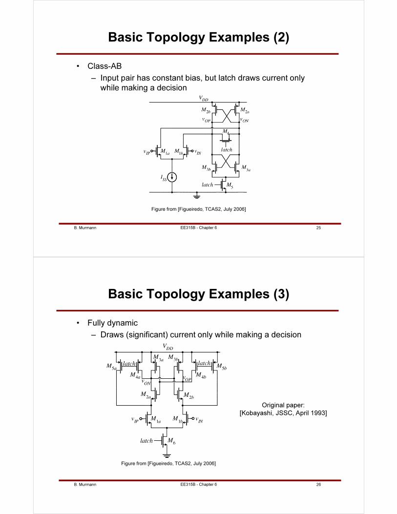
B. Murmann 25
Basic Topology Examples (2)
• Class-AB
– Input pair has constant bias, but latch draws current only
while making a decision
EE315B - Chapter 6
Figure from [Figueiredo, TCAS2, July 2006]
B. Murmann 26
Basic Topology Examples (3)
• Fully dynamic
– Draws (significant) current only while making a decision
EE315B - Chapter 6
Figure from [Figueiredo, TCAS2, July 2006]
Original paper:
[Kobayashi, JSSC, April 1993]
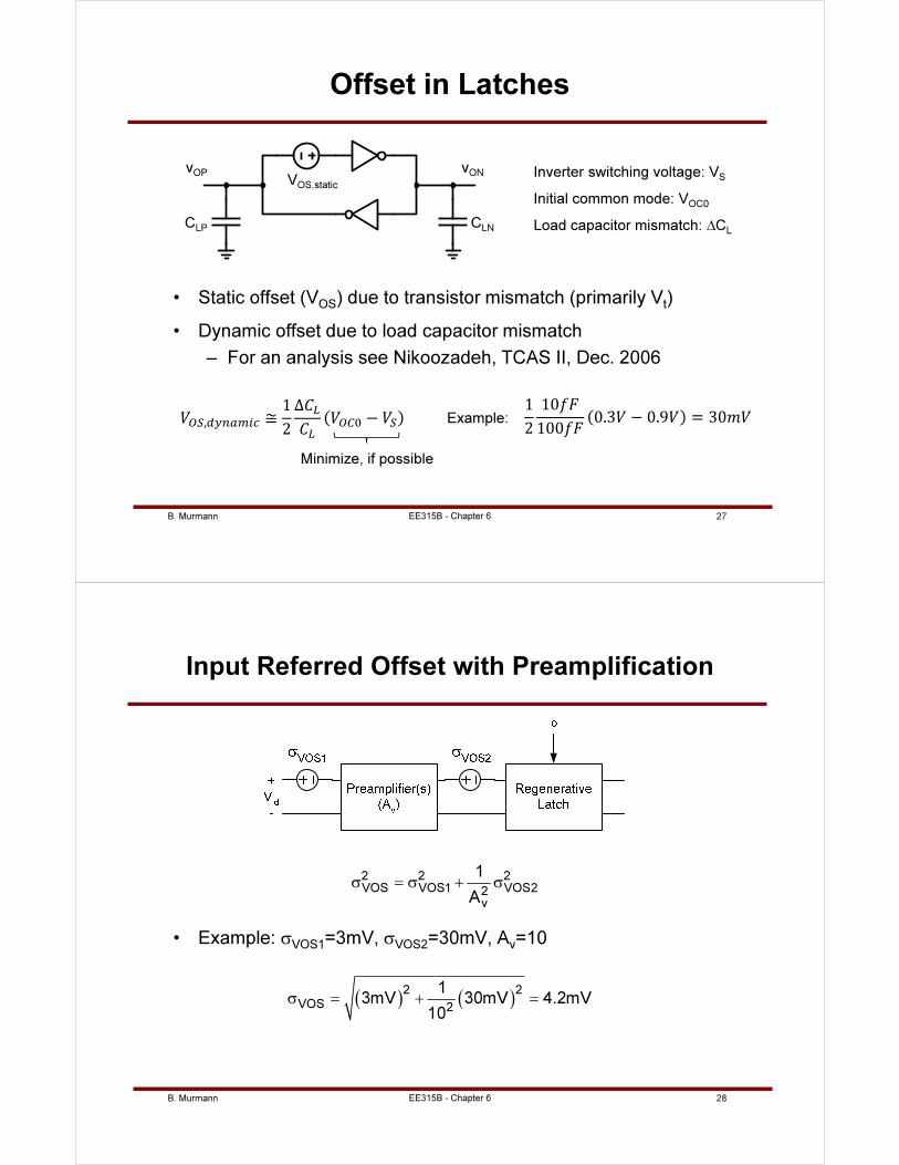
B. Murmann 27
Offset in Latches
• Static offset (VOS) due to transistor mismatch (primarily Vt)
• Dynamic offset due to load capacitor mismatch
– For an analysis see Nikoozadeh, TCAS II, Dec. 2006
EE315B - Chapter 6
VOS,static
CLP CLN
vOP vON Inverter switching voltage: VS
Initial common mode: VOC0
Load capacitor mismatch: ∆CL
, ≅1
2
Δ
− Example:
1
2
10
1000.3 − 0.9 = 30
Minimize, if possible
B. Murmann 28EE315B - Chapter 6
Input Referred Offset with Preamplification
• Example: σVOS1=3mV, σVOS2=30mV, Av=10
2 2 2
VOS VOS1 VOS22
v
1
Aσ = σ + σ
( ) ( )2 2
VOS 2
13mV 30mV 4.2mV
10σ = + =

B. Murmann 29
Dealing With Offset
• Options depend strongly on the application context
• May use an ADC architecture that inherently tolerates offset
– More later
• May use a relatively coarse tuning mechanism
– E.g. tune offset to lie within ½ LSB at the 6-bit level
• May have to apply precision techniques
– Autozeroing, etc. (see EE315A), for high-end instrumentation
• Simply use large transistors
– Usually not power efficient
EE315B - Chapter 6
B. Murmann 30
Example: Coarse Offset Tuning
• The circuit below uses capacitve imbalance to tune the offset
– An example of using a "bug" as a feature
– See e.g. Van der Plas, ISSCC 2006
• Watch out for PSRR degradation due to circuit imbalance
EE315B - Chapter 6
B. Murmann 31EE315B - Chapter 6
Example: Precision Comparator
• Used in the AD7671, 16-bit, 1-MS/s successive approximation ADC
• Uses cascaded output series offset cancellation (see EE315A)
[http://www.elecdesign.com/Articles/Index.cfm?ArticleID=3956]
B. Murmann 32
Electronic Noise in Latch Comparators
• Class-A topology
– Integrate noise at regenerative node over all frequencies and refer to the input α·kT/CL
– See Opris, Electronics Letters, July 1997
• Dynamic topology
– Very hard to analyze due to the time variant behavior
– See Nuzzo, IEEE TCAS1, July 2008
– Fortunately, the end result is not too far from class-A-like noise estimation in the decision point α·kT/CL
EE315B - Chapter 6
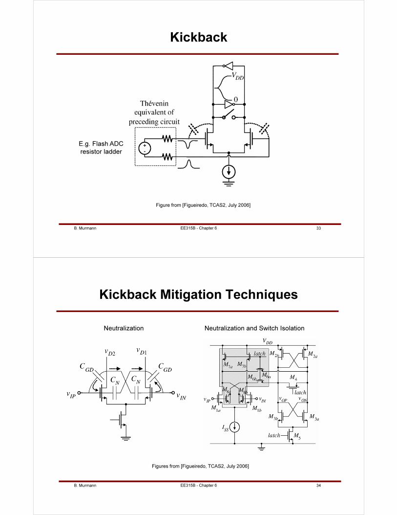
B. Murmann 33
Kickback
EE315B - Chapter 6
Figure from [Figueiredo, TCAS2, July 2006]
E.g. Flash ADC
resistor ladder
B. Murmann 34
Kickback Mitigation Techniques
EE315B - Chapter 6
Figures from [Figueiredo, TCAS2, July 2006]
Neutralization Neutralization and Switch Isolation
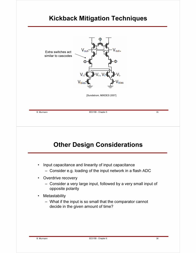
B. Murmann 35
Kickback Mitigation Techniques
EE315B - Chapter 6
[Sundstrom, MIXDES 2007]
Extra switches act
similar to cascodes
B. Murmann 36
Other Design Considerations
• Input capacitance and linearity of input capacitance
– Consider e.g. loading of the input network in a flash ADC
• Overdrive recovery
– Consider a very large input, followed by a very small input of
opposite polarity
• Metastability
– What if the input is so small that the comparator cannot
decide in the given amount of time?
EE315B - Chapter 6
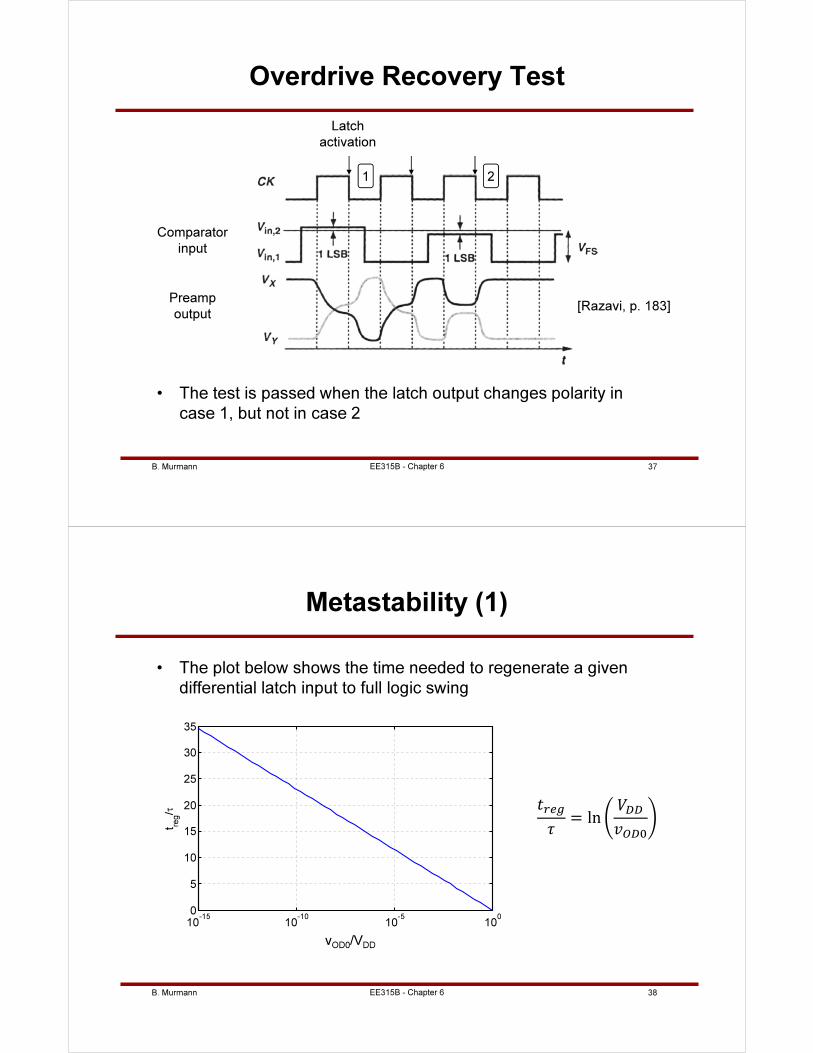
B. Murmann 37
Overdrive Recovery Test
• The test is passed when the latch output changes polarity in
case 1, but not in case 2
EE315B - Chapter 6
[Razavi, p. 183]
Comparator
input
Preamp
output
Latch
activation
1 2
B. Murmann 38
10-15
10-10
10-5
100
0
5
10
15
20
25
30
35
v /V
t reg/τ
Metastability (1)
• The plot below shows the time needed to regenerate a given
differential latch input to full logic swing
EE315B - Chapter 6
= ln
vOD0/VDD
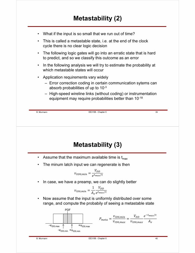
B. Murmann 39
Metastability (2)
• What if the input is so small that we run out of time?
• This is called a metastable state, i.e. at the end of the clock
cycle there is no clear logic decision
• The following logic gates will go into an erratic state that is hard
to predict, and so we classify this outcome as an error
• In the following analysis we will try to estimate the probability at
which metastable states will occur
• Application requirements vary widely
– Error correction coding in certain communication sytems can
absorb probabilities of up to 10-3
– High-speed wireline links (without coding) or instrumentation
equipment may require probabilities better than 10-18
EE315B - Chapter 6
B. Murmann 40EE315B - Chapter 6
Metastability (3)
• Assume that the maximum available time is tmax
• The minum latch input we can regenerate is then
, =
/
• In case, we have a preamp, we can do slightly better
, =1
/
• Now assume that the input is uniformly distributed over some
range, and compute the probabily of seeing a metastable state
+vID0,max-vID0,max
+vID0,min-vID0,min
=,
,
=
,
/
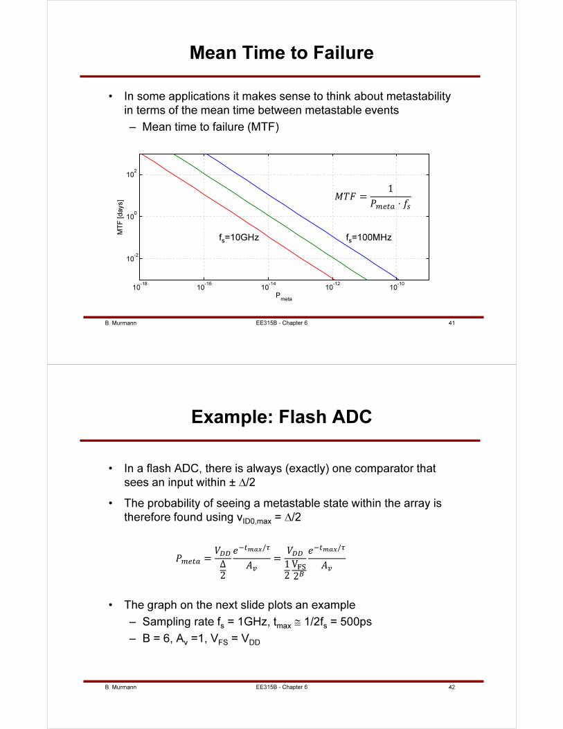
B. Murmann 41
Mean Time to Failure
• In some applications it makes sense to think about metastability
in terms of the mean time between metastable events
– Mean time to failure (MTF)
EE315B - Chapter 6
10-18
10-16
10-14
10-12
10-10
10-2
100
102
Pmeta
MT
F [d
ays] =
1
⋅
fs=10GHz fs=100MHz
B. Murmann 42
Example: Flash ADC
• In a flash ADC, there is always (exactly) one comparator that
sees an input within ± ∆/2
• The probability of seeing a metastable state within the array is
therefore found using vID0,max = ∆/2
EE315B - Chapter 6
=Δ2
/
=12V2
/
• The graph on the next slide plots an example
– Sampling rate fs = 1GHz, tmax ≅ 1/2fs = 500ps
– B = 6, Av =1, VFS = VDD
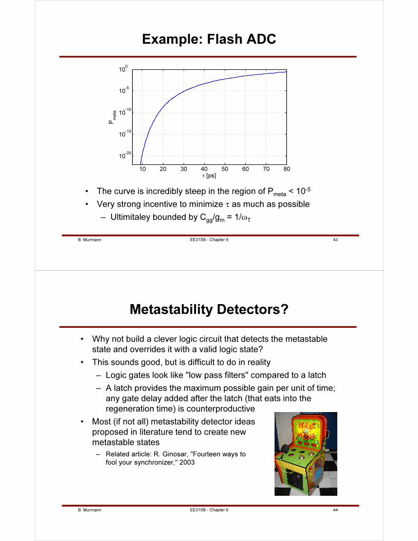
B. Murmann 43
Example: Flash ADC
• The curve is incredibly steep in the region of Pmeta < 10-5
• Very strong incentive to minimize τ as much as possible
– Ultimitaley bounded by Cgg/gm = 1/ωT
EE315B - Chapter 6
10 20 30 40 50 60 70 80
10-20
10-15
10-10
10-5
100
Pmeta
τ [ps]
B. Murmann 44
Metastability Detectors?
• Why not build a clever logic circuit that detects the metastable
state and overrides it with a valid logic state?
• This sounds good, but is difficult to do in reality
– Logic gates look like "low pass filters" compared to a latch
– A latch provides the maximum possible gain per unit of time;
any gate delay added after the latch (that eats into the
regeneration time) is counterproductive
• Most (if not all) metastability detector ideas
proposed in literature tend to create new
metastable states
– Related article: R. Ginosar, "Fourteen ways to
fool your synchronizer," 2003
EE315B - Chapter 6
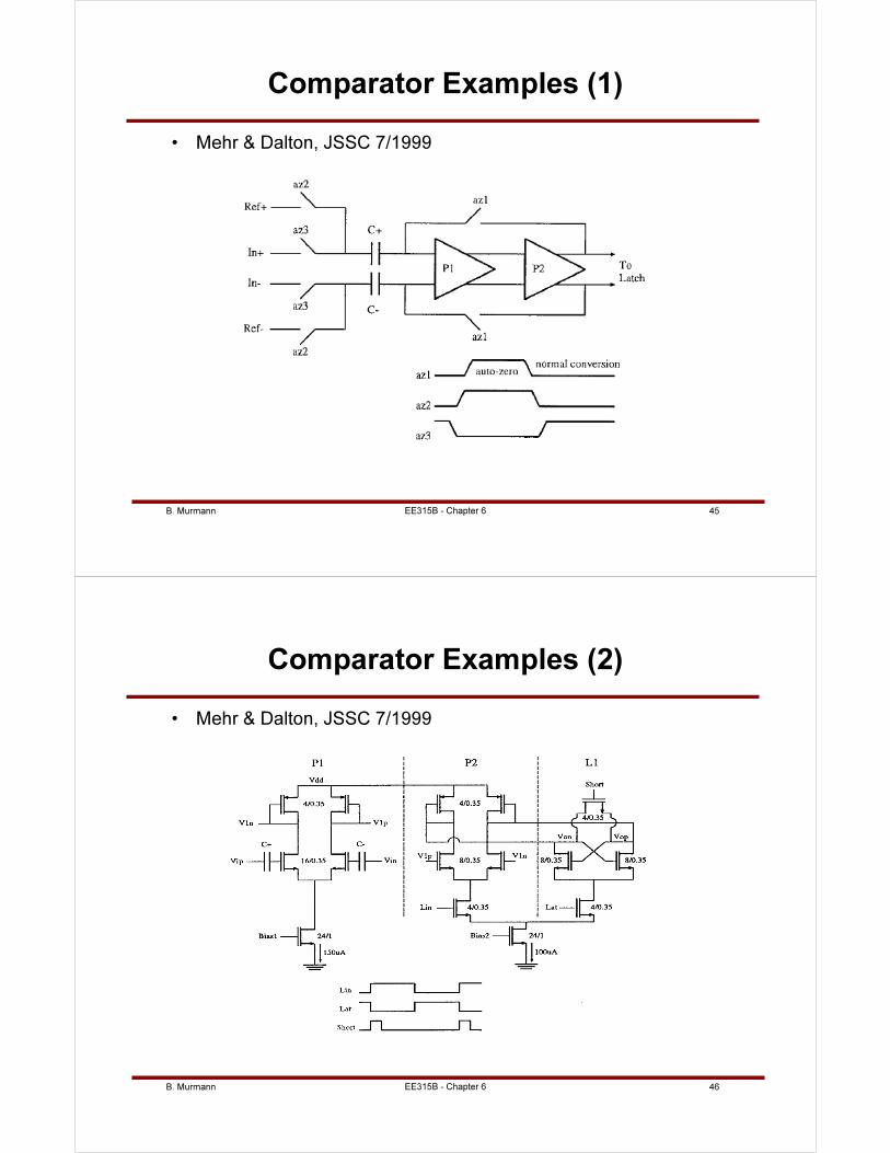
B. Murmann 45EE315B - Chapter 6
Comparator Examples (1)
• Mehr & Dalton, JSSC 7/1999
B. Murmann 46EE315B - Chapter 6
Comparator Examples (2)
• Mehr & Dalton, JSSC 7/1999
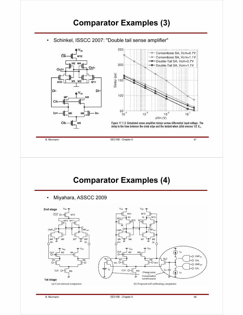
B. Murmann 47EE315B - Chapter 6
Comparator Examples (3)
• Schinkel, ISSCC 2007: "Double tail sense amplifier"
B. Murmann 48EE315B - Chapter 6
Comparator Examples (4)
• Miyahara, ASSCC 2009
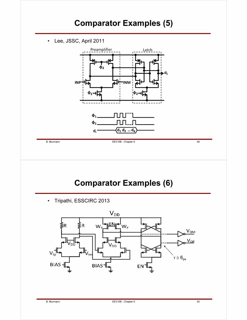
B. Murmann 49EE315B - Chapter 6
Comparator Examples (5)
• Lee, JSSC, April 2011
B. Murmann 50EE315B - Chapter 6
Comparator Examples (6)
• Tripathi, ESSCIRC 2013
τ ≅ 6ps
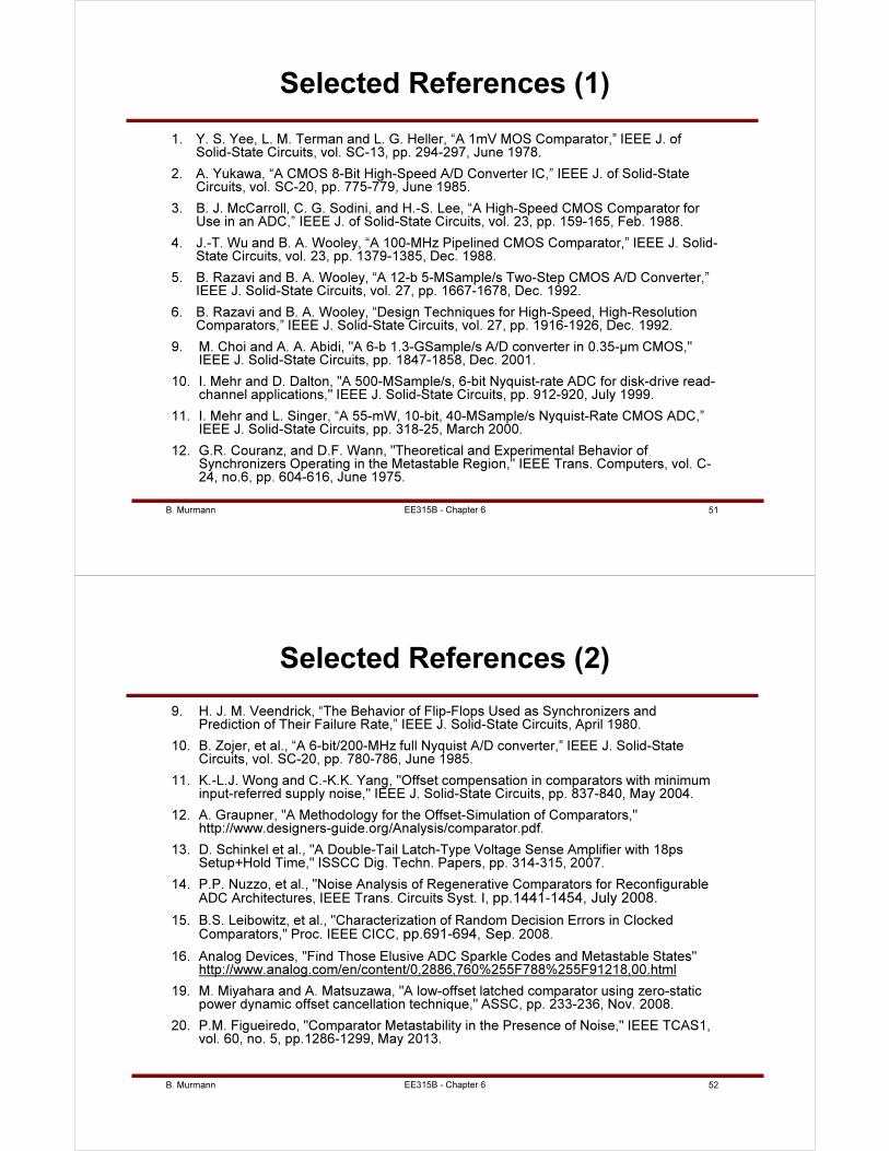
B. Murmann 51EE315B - Chapter 6
Selected References (1)
1. Y. S. Yee, L. M. Terman and L. G. Heller, “A 1mV MOS Comparator,” IEEE J. of Solid-State Circuits, vol. SC-13, pp. 294-297, June 1978.
2. A. Yukawa, “A CMOS 8-Bit High-Speed A/D Converter IC,” IEEE J. of Solid-State Circuits, vol. SC-20, pp. 775-779, June 1985.
3. B. J. McCarroll, C. G. Sodini, and H.-S. Lee, “A High-Speed CMOS Comparator for Use in an ADC,” IEEE J. of Solid-State Circuits, vol. 23, pp. 159-165, Feb. 1988.
4. J.-T. Wu and B. A. Wooley, “A 100-MHz Pipelined CMOS Comparator,” IEEE J. Solid-State Circuits, vol. 23, pp. 1379-1385, Dec. 1988.
5. B. Razavi and B. A. Wooley, “A 12-b 5-MSample/s Two-Step CMOS A/D Converter,” IEEE J. Solid-State Circuits, vol. 27, pp. 1667-1678, Dec. 1992.
6. B. Razavi and B. A. Wooley, “Design Techniques for High-Speed, High-Resolution Comparators,” IEEE J. Solid-State Circuits, vol. 27, pp. 1916-1926, Dec. 1992.
9. M. Choi and A. A. Abidi, "A 6-b 1.3-GSample/s A/D converter in 0.35-µm CMOS," IEEE J. Solid-State Circuits, pp. 1847-1858, Dec. 2001.
10. I. Mehr and D. Dalton, "A 500-MSample/s, 6-bit Nyquist-rate ADC for disk-drive read-channel applications," IEEE J. Solid-State Circuits, pp. 912-920, July 1999.
11. I. Mehr and L. Singer, “A 55-mW, 10-bit, 40-MSample/s Nyquist-Rate CMOS ADC,” IEEE J. Solid-State Circuits, pp. 318-25, March 2000.
12. G.R. Couranz, and D.F. Wann, "Theoretical and Experimental Behavior of Synchronizers Operating in the Metastable Region," IEEE Trans. Computers, vol. C-24, no.6, pp. 604-616, June 1975.
B. Murmann 52EE315B - Chapter 6
Selected References (2)
9. H. J. M. Veendrick, “The Behavior of Flip-Flops Used as Synchronizers and Prediction of Their Failure Rate,” IEEE J. Solid-State Circuits, April 1980.
10. B. Zojer, et al., “A 6-bit/200-MHz full Nyquist A/D converter,” IEEE J. Solid-State Circuits, vol. SC-20, pp. 780-786, June 1985.
11. K.-L.J. Wong and C.-K.K. Yang, "Offset compensation in comparators with minimum input-referred supply noise," IEEE J. Solid-State Circuits, pp. 837-840, May 2004.
12. A. Graupner, "A Methodology for the Offset-Simulation of Comparators," http://www.designers-guide.org/Analysis/comparator.pdf.
13. D. Schinkel et al., "A Double-Tail Latch-Type Voltage Sense Amplifier with 18ps Setup+Hold Time," ISSCC Dig. Techn. Papers, pp. 314-315, 2007.
14. P.P. Nuzzo, et al., "Noise Analysis of Regenerative Comparators for Reconfigurable ADC Architectures, IEEE Trans. Circuits Syst. I, pp.1441-1454, July 2008.
15. B.S. Leibowitz, et al., "Characterization of Random Decision Errors in Clocked Comparators," Proc. IEEE CICC, pp.691-694, Sep. 2008.
16. Analog Devices, "Find Those Elusive ADC Sparkle Codes and Metastable States" http://www.analog.com/en/content/0,2886,760%255F788%255F91218,00.html
19. M. Miyahara and A. Matsuzawa, "A low-offset latched comparator using zero-static power dynamic offset cancellation technique," ASSC, pp. 233-236, Nov. 2008.
20. P.M. Figueiredo, "Comparator Metastability in the Presence of Noise," IEEE TCAS1, vol. 60, no. 5, pp.1286-1299, May 2013.
B. Murmann 1EE315B - Chapter 7
Flash ADCs
Boris Murmann
Stanford University
Copyright © 2013 by Boris Murmann
B. Murmann 2EE315B - Chapter 7
Nyquist ADC Architectures
• Nyquist rate
– Word-at-a-time
• Flash ADC
• Instantaneous comparison with 2B-1 reference levels
– Multi-step
• E.g. pipeline ADCs
• Coarse conversion, followed by fine conversion of residuum
– Bit-at-a-time
• E.g. successive approximation ADCs
• Conversion via a binary search algorithm
– Level-at-a-time
• E.g. single or dual slope ADCs
• Input is converted by measuring the time it takes to
charge/discharge a capacitor from/to input voltage
SPEED
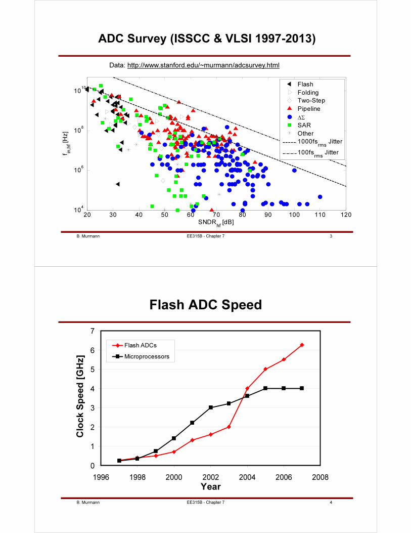
B. Murmann 3EE315B - Chapter 7
ADC Survey (ISSCC & VLSI 1997-2013)
Data: http://www.stanford.edu/~murmann/adcsurvey.html
20 30 40 50 60 70 80 90 100 110 12010
4
106
108
1010
SNDRhf
[dB]
f in,hf [
Hz]
Flash
Folding
Two-Step
Pipeline
∆Σ
SAR
Other
1000fsrms
Jitter
100fsrms
Jitter
B. Murmann 4
Flash ADC Speed
0
1
2
3
4
5
6
7
1996 1998 2000 2002 2004 2006 2008
Year
Clo
ck S
peed
[G
Hz]
Flash ADCs
Microprocessors
EE315B - Chapter 7
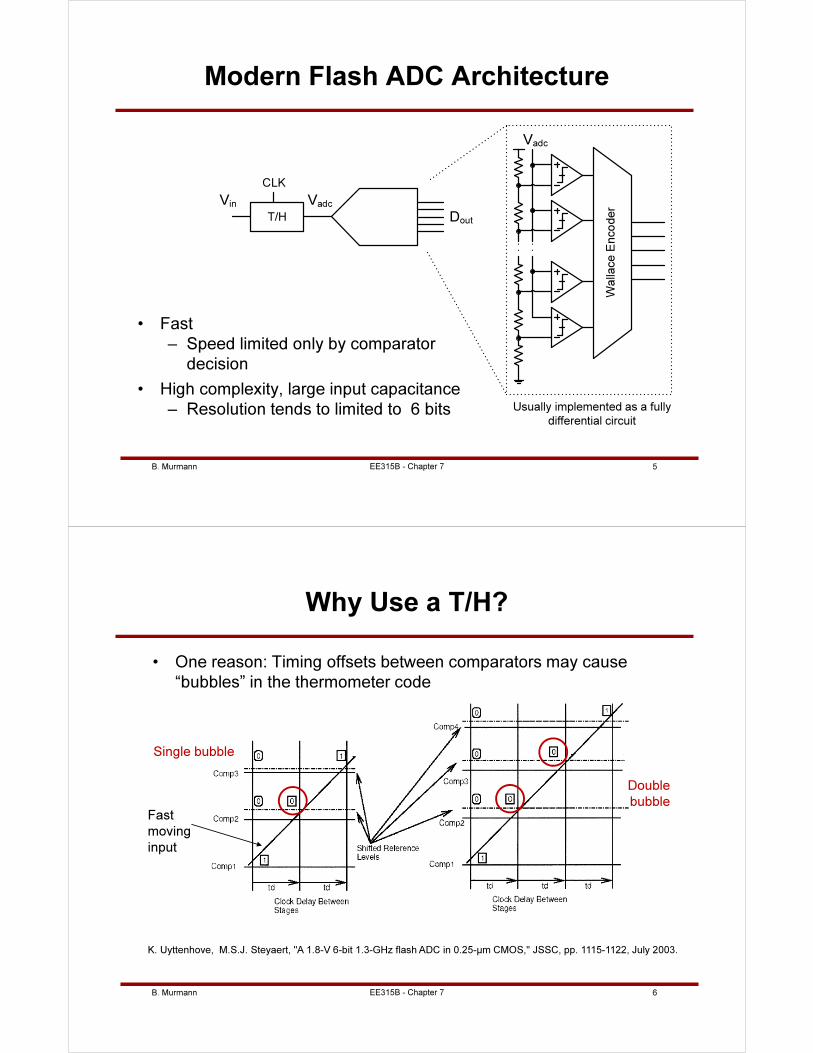
B. Murmann 5EE315B - Chapter 7
Modern Flash ADC Architecture
• Fast
– Speed limited only by comparator
decision
• High complexity, large input capacitance
– Resolution tends to limited to 6 bits
T/H
Wallace E
nco
der
Dout
CLK
Vin
Vadc
Vadc
Usually implemented as a fully
differential circuit
B. Murmann 6
Why Use a T/H?
• One reason: Timing offsets between comparators may cause
“bubbles” in the thermometer code
EE315B - Chapter 7
K. Uyttenhove, M.S.J. Steyaert, "A 1.8-V 6-bit 1.3-GHz flash ADC in 0.25-μm CMOS," JSSC, pp. 1115-1122, July 2003.
Fast
moving
input
Single bubble
Double
bubble
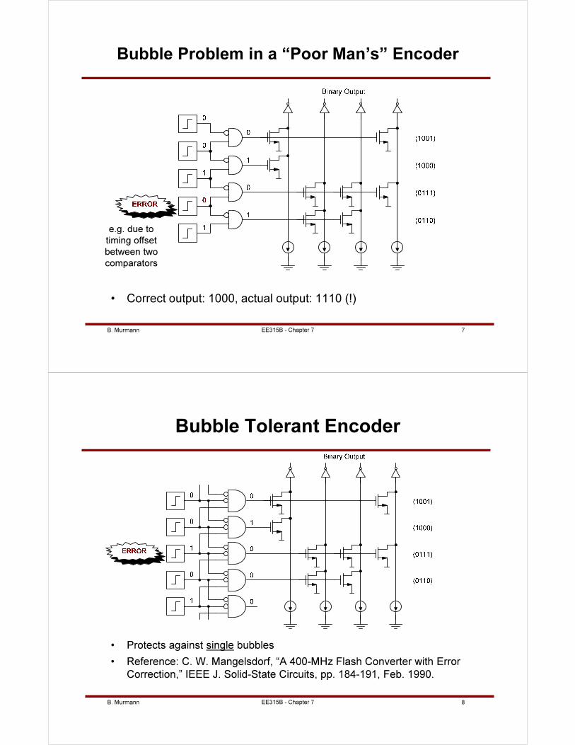
B. Murmann 7EE315B - Chapter 7
Bubble Problem in a “Poor Man’s” Encoder
• Correct output: 1000, actual output: 1110 (!)
e.g. due to
timing offset
between two
comparators
B. Murmann 8EE315B - Chapter 7
Bubble Tolerant Encoder
• Protects against single bubbles
• Reference: C. W. Mangelsdorf, “A 400-MHz Flash Converter with Error
Correction,” IEEE J. Solid-State Circuits, pp. 184-191, Feb. 1990.
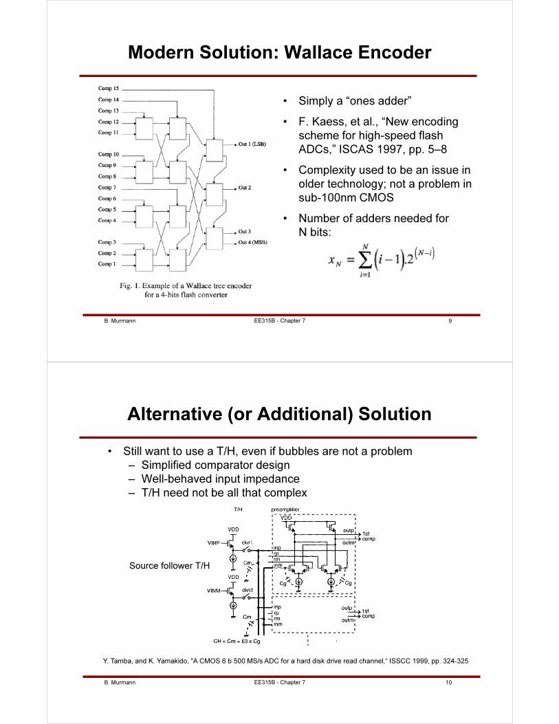
B. Murmann 9
Modern Solution: Wallace Encoder
• Simply a “ones adder”
• F. Kaess, et al., “New encoding
scheme for high-speed flash
ADCs,” ISCAS 1997, pp. 5–8
• Complexity used to be an issue in
older technology; not a problem in
sub-100nm CMOS
• Number of adders needed for
N bits:
EE315B - Chapter 7
B. Murmann 10
Alternative (or Additional) Solution
• Still want to use a T/H, even if bubbles are not a problem
– Simplified comparator design
– Well-behaved input impedance
– T/H need not be all that complex
EE315B - Chapter 7
Y. Tamba, and K. Yamakido, "A CMOS 6 b 500 MS/s ADC for a hard disk drive read channel,“ ISSCC 1999, pp. 324-325
Source follower T/H
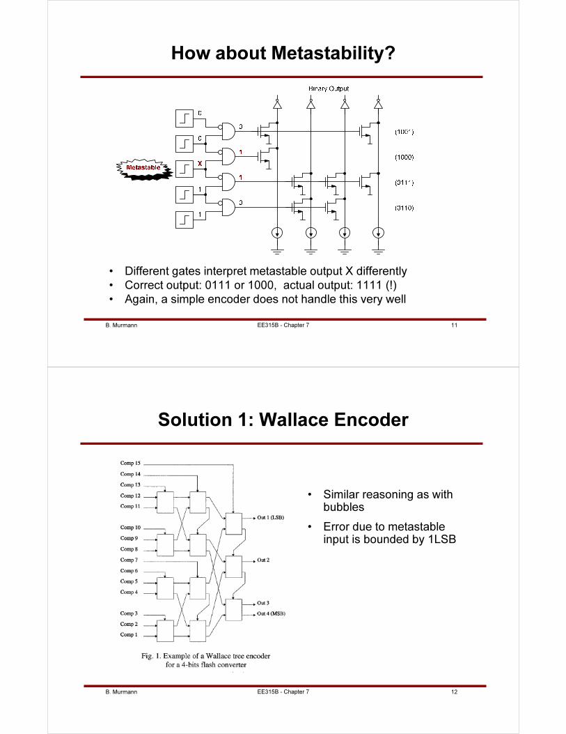
B. Murmann 11EE315B - Chapter 7
How about Metastability?
• Different gates interpret metastable output X differently
• Correct output: 0111 or 1000, actual output: 1111 (!)
• Again, a simple encoder does not handle this very well
B. Murmann 12EE315B - Chapter 7
Solution 1: Wallace Encoder
• Similar reasoning as with bubbles
• Error due to metastable input is bounded by 1LSB

B. Murmann 13EE315B - Chapter 7
Solution 2: Latch Pipelining
• Use additional latches to create extra gain before generating decoder signals
• Usually too power hungry and area inefficient
B. Murmann 14EE315B - Chapter 7
Solution 2: Gray Encoding
• Each Ti affects only one Gi
– Avoids disagreement
of interpretation by
multiple gates
Thermometer Code Gray Binary
T1 T2 T3 T4 T5 T6 T7 G3 G2 G1 B3 B2 B1
0 0 0 0 0 0 0 0 0 0 0 0 0
1 0 0 0 0 0 0 0 0 1 0 0 1
1 1 0 0 0 0 0 0 1 1 0 1 0
1 1 1 0 0 0 0 0 1 0 0 1 1
1 1 1 1 0 0 0 1 1 0 1 0 0
1 1 1 1 1 0 0 1 1 1 1 0 1
1 1 1 1 1 1 0 1 0 1 1 1 0
1 1 1 1 1 1 1 1 0 0 1 1 1
G3 G2 G1
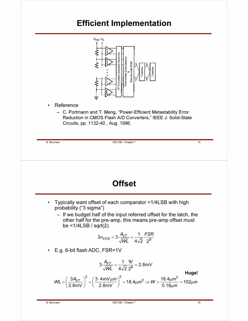
B. Murmann 15EE315B - Chapter 7
Efficient Implementation
• Reference
– C. Portmann and T. Meng, “Power-Efficient Metastability Error
Reduction in CMOS Flash A/D Converters,” IEEE J. Solid-State
Circuits, pp. 1132-40 , Aug. 1996.
B. Murmann 16EE315B - Chapter 7
Offset
• Typically want offset of each comparator <1/4LSB with high probability (“3 sigma”)
– If we budget half of the input referred offset for the latch, the other half for the pre-amp, this means pre-amp offset must be <1/4LSB / sqrt(2)
13 3
4 2 2
VTVOS B
A FSR
WLσ = <
6
2 2 22
1 13 2 8
4 2 2
3 3 4 18 418 4 102
2 8 2 8 0 18
VT
VT
A V. mV
WL
A mV m . mWL . m W m
. mV . mV . m
< =
⋅ µ µ > = = µ ⇒ > = µ µ
Huge!
• E.g. 6-bit flash ADC, FSR=1V
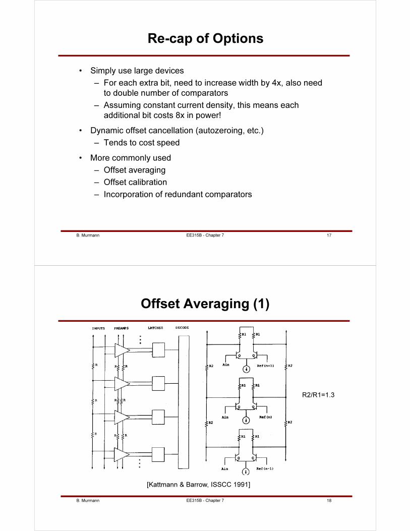
B. Murmann 17EE315B - Chapter 7
Re-cap of Options
• Simply use large devices
– For each extra bit, need to increase width by 4x, also need
to double number of comparators
– Assuming constant current density, this means each
additional bit costs 8x in power!
• Dynamic offset cancellation (autozeroing, etc.)
– Tends to cost speed
• More commonly used
– Offset averaging
– Offset calibration
– Incorporation of redundant comparators
B. Murmann 18EE315B - Chapter 7
Offset Averaging (1)
[Kattmann & Barrow, ISSCC 1991]
R2/R1=1.3
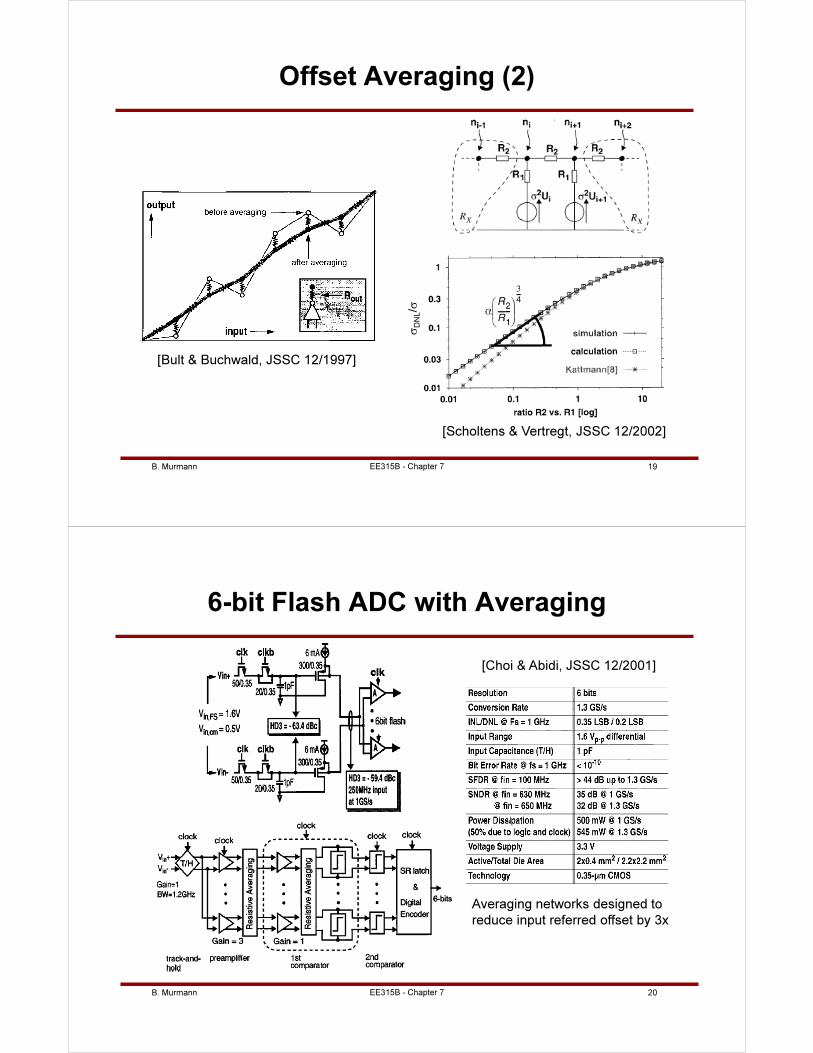
B. Murmann 19EE315B - Chapter 7
Offset Averaging (2)
[Bult & Buchwald, JSSC 12/1997]
[Scholtens & Vertregt, JSSC 12/2002]
σDNL/σ
B. Murmann 20EE315B - Chapter 7
6-bit Flash ADC with Averaging
[Choi & Abidi, JSSC 12/2001]
Averaging networks designed to
reduce input referred offset by 3x
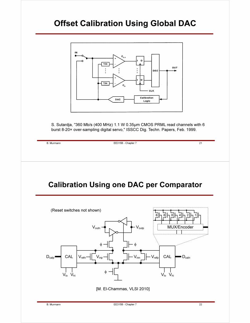
B. Murmann 21EE315B - Chapter 7
Offset Calibration Using Global DAC
S. Sutardja, "360 Mb/s (400 MHz) 1.1 W 0.35μm CMOS PRML read channels with 6
burst 8-20× over-sampling digital servo," ISSCC Dig. Techn. Papers, Feb. 1999.
B. Murmann 22
Calibration Using one DAC per Comparator
CAL
Vlo Vhi
DcalnCAL
Vlo Vhi
Dcalp
MUX/Encoder
124888
VinpVrefn
φ
Vinn Vrefp
φ φ
Voutn Voutp
[M. El-Chammas, VLSI 2010]
(Reset switches not shown)
EE315B - Chapter 7
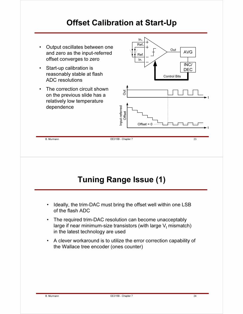
B. Murmann 23
Offset Calibration at Start-Up
• Output oscillates between one
and zero as the input-referred
offset converges to zero
• Start-up calibration is
reasonably stable at flash
ADC resolutions
• The correction circuit shown
on the previous slide has a
relatively low temperature
dependence
EE315B - Chapter 7
In-
Ref+
Ref-
In+
Out
Ou
tIn
pu
t-re
ferr
ed
Off
set
AVG
Control Bits
Offset = 0
INC/
DEC
t
t
B. Murmann 24
Tuning Range Issue (1)
• Ideally, the trim-DAC must bring the offset well within one LSB
of the flash ADC
• The required trim-DAC resolution can become unacceptably
large if near minimum-size transistors (with large Vtmismatch)
in the latest technology are used
• A clever workaround is to utilize the error correction capability of
the Wallace tree encoder (ones counter)
EE315B - Chapter 7
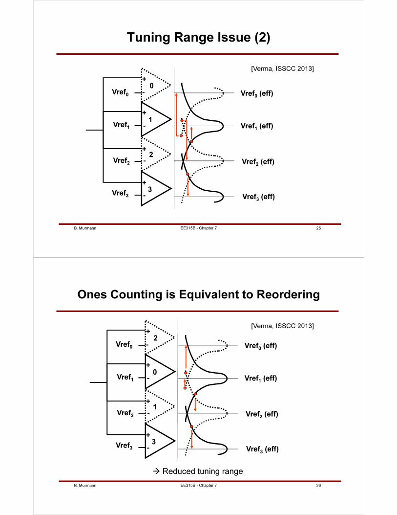
B. Murmann 25
Tuning Range Issue (2)
0
1
2
3
Vref0
Vref1
Vref2
Vref3
+
+
+
+
-
-
-
-
Vref3
(eff)
Vref2
(eff)
Vref1
(eff)
Vref0
(eff)
[Verma, ISSCC 2013]
EE315B - Chapter 7
B. Murmann 26
Ones Counting is Equivalent to Reordering
2
0
1
3
Vref0
Vref1
Vref2
Vref3
+
+
+
+
-
-
-
-
Vref3
(eff)
Vref2
(eff)
Vref1
(eff)
Vref0
(eff)
[Verma, ISSCC 2013]
Reduced tuning range
EE315B - Chapter 7
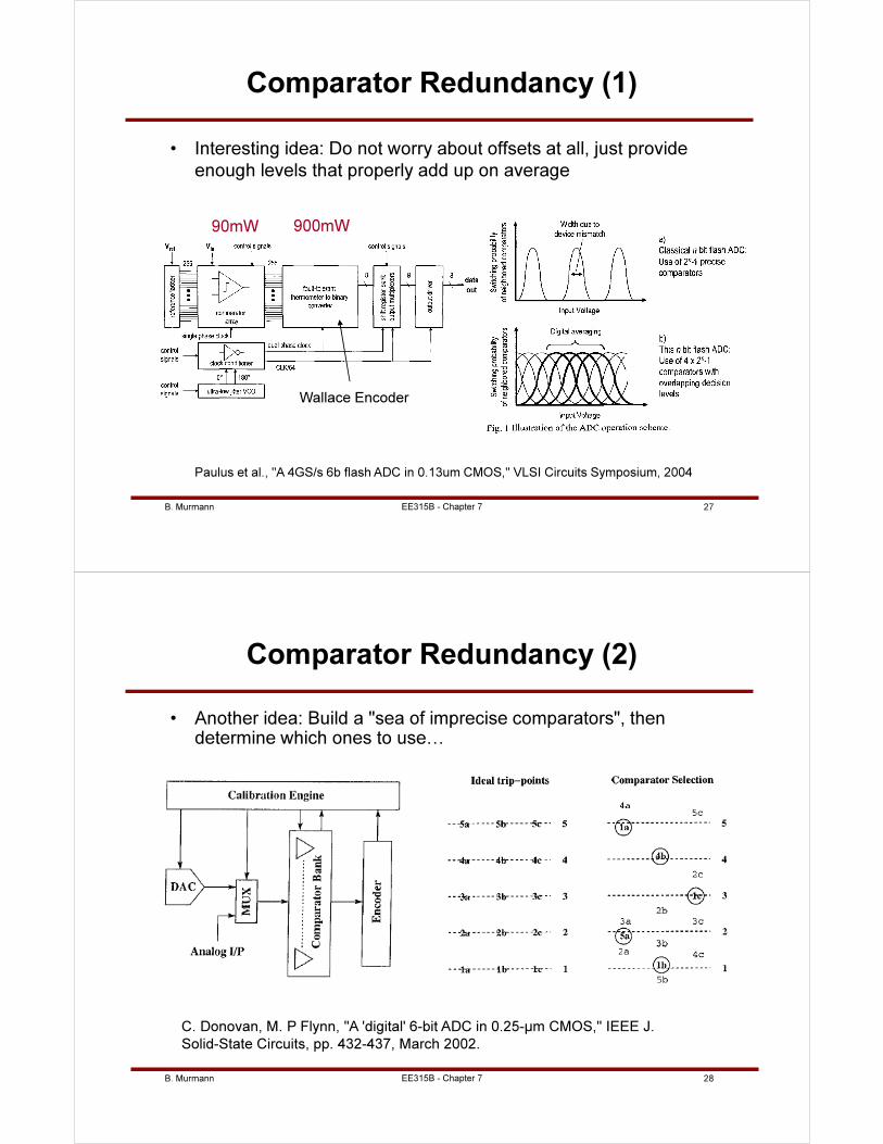
B. Murmann 27
Comparator Redundancy (1)
• Interesting idea: Do not worry about offsets at all, just provide
enough levels that properly add up on average
EE315B - Chapter 7
90mW 900mW
Paulus et al., "A 4GS/s 6b flash ADC in 0.13um CMOS," VLSI Circuits Symposium, 2004
Wallace Encoder
B. Murmann 28EE315B - Chapter 7
Comparator Redundancy (2)
• Another idea: Build a "sea of imprecise comparators", then determine which ones to use…
C. Donovan, M. P Flynn, "A 'digital' 6-bit ADC in 0.25-μm CMOS," IEEE J.
Solid-State Circuits, pp. 432-437, March 2002.
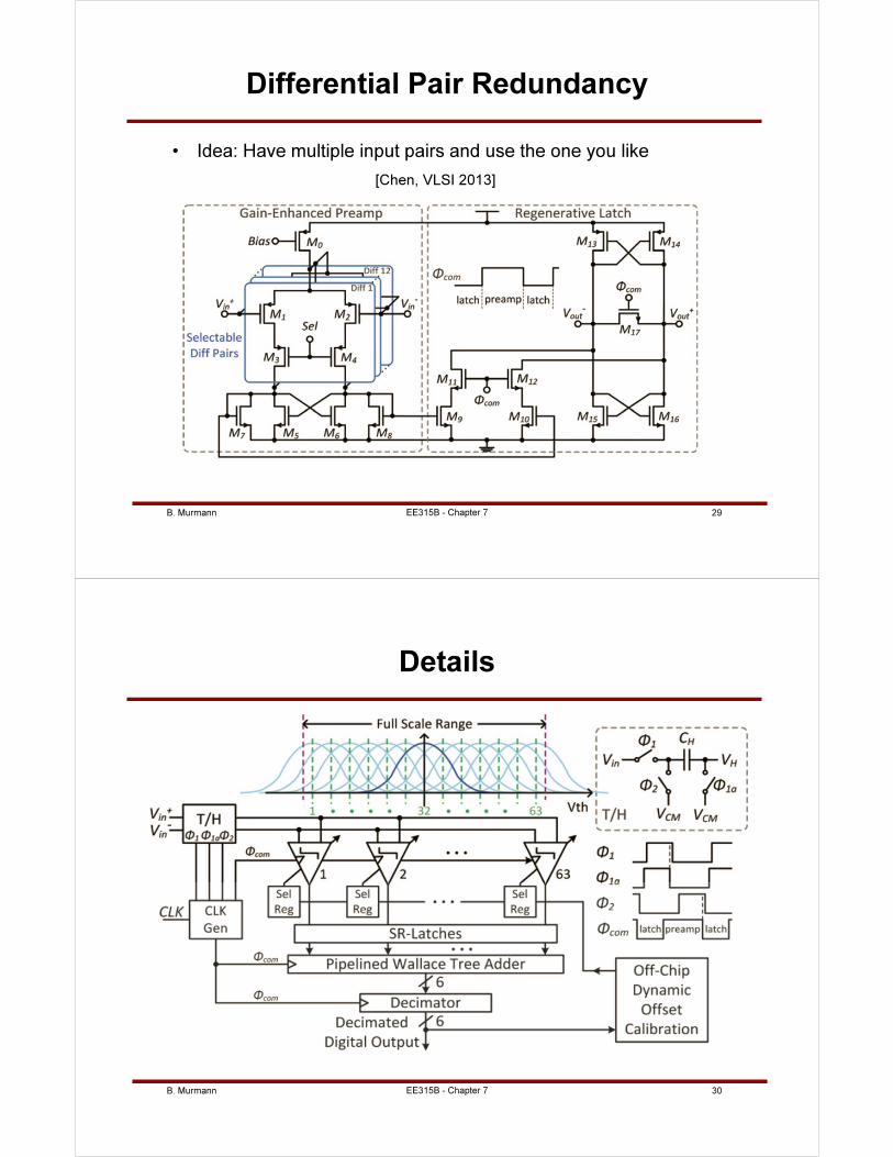
B. Murmann 29
Differential Pair Redundancy
[Chen, VLSI 2013]
• Idea: Have multiple input pairs and use the one you like
EE315B - Chapter 7
B. Murmann 30
Details
EE315B - Chapter 7
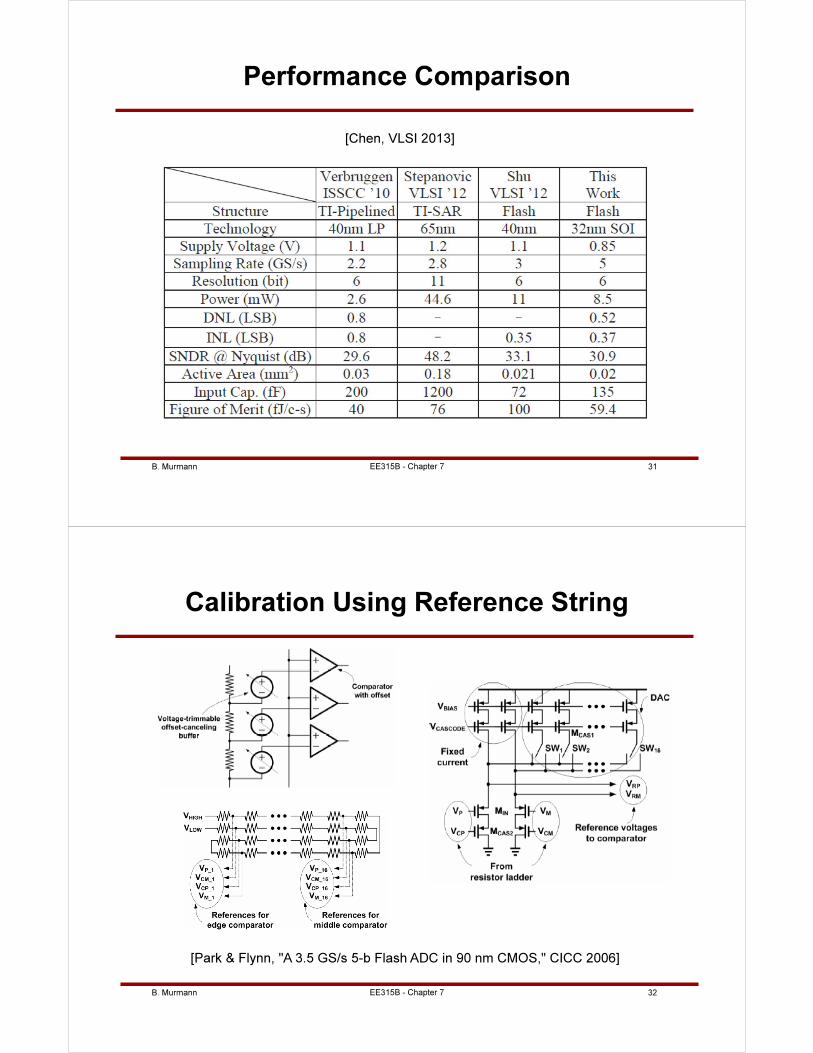
B. Murmann 31
Performance Comparison
[Chen, VLSI 2013]
EE315B - Chapter 7
B. Murmann 32EE315B - Chapter 7
Calibration Using Reference String
[Park & Flynn, "A 3.5 GS/s 5-b Flash ADC in 90 nm CMOS," CICC 2006]
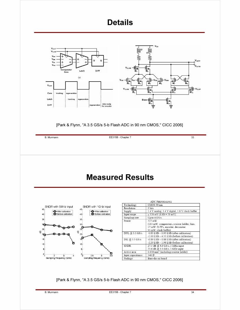
B. Murmann 33
Details
EE315B - Chapter 7
[Park & Flynn, "A 3.5 GS/s 5-b Flash ADC in 90 nm CMOS," CICC 2006]
B. Murmann 34EE315B - Chapter 7
Measured Results
[Park & Flynn, "A 3.5 GS/s 5-b Flash ADC in 90 nm CMOS," CICC 2006]
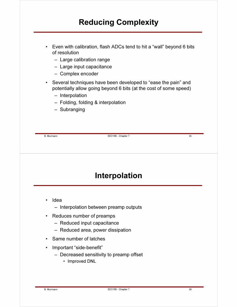
B. Murmann 35EE315B - Chapter 7
Reducing Complexity
• Even with calibration, flash ADCs tend to hit a “wall” beyond 6 bits
of resolution
– Large calibration range
– Large input capacitance
– Complex encoder
• Several techniques have been developed to “ease the pain” and
potentially allow going beyond 6 bits (at the cost of some speed)
– Interpolation
– Folding, folding & interpolation
– Subranging
B. Murmann 36EE315B - Chapter 7
Interpolation
• Idea
– Interpolation between preamp outputs
• Reduces number of preamps
– Reduced input capacitance
– Reduced area, power dissipation
• Same number of latches
• Important “side-benefit”
– Decreased sensitivity to preamp offset
• Improved DNL
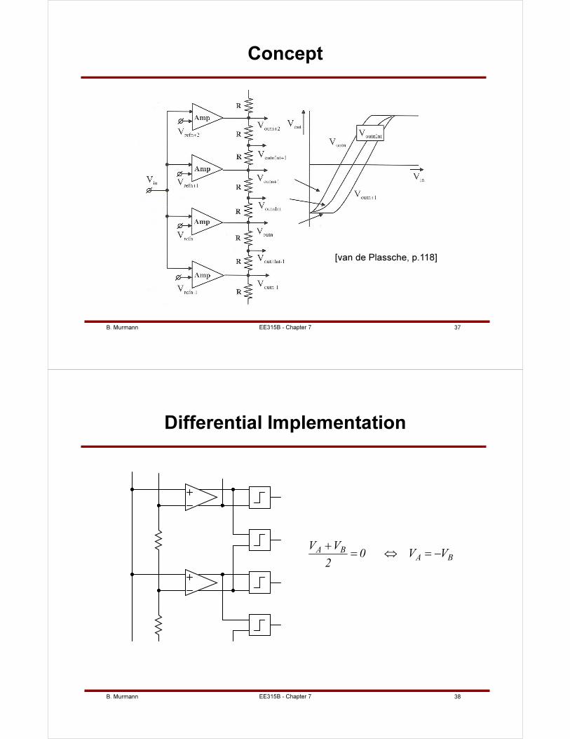
B. Murmann 37EE315B - Chapter 7
Concept
[van de Plassche, p.118]
B. Murmann 38EE315B - Chapter 7
Differential Implementation
BA
BAVV0
2
VV−=⇔=
+
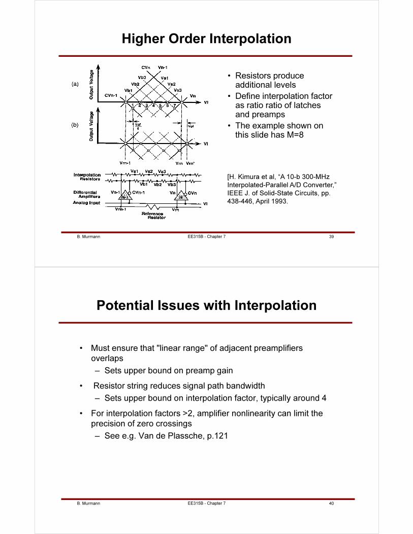
B. Murmann 39EE315B - Chapter 7
Higher Order Interpolation
• Resistors produce additional levels
• Define interpolation factor as ratio ratio of latches and preamps
• The example shown on this slide has M=8
[H. Kimura et al, “A 10-b 300-MHz
Interpolated-Parallel A/D Converter,”
IEEE J. of Solid-State Circuits, pp.
438-446, April 1993.
B. Murmann 40EE315B - Chapter 7
Potential Issues with Interpolation
• Must ensure that "linear range" of adjacent preamplifiers
overlaps
– Sets upper bound on preamp gain
• Resistor string reduces signal path bandwidth
– Sets upper bound on interpolation factor, typically around 4
• For interpolation factors >2, amplifier nonlinearity can limit the
precision of zero crossings
– See e.g. Van de Plassche, p.121
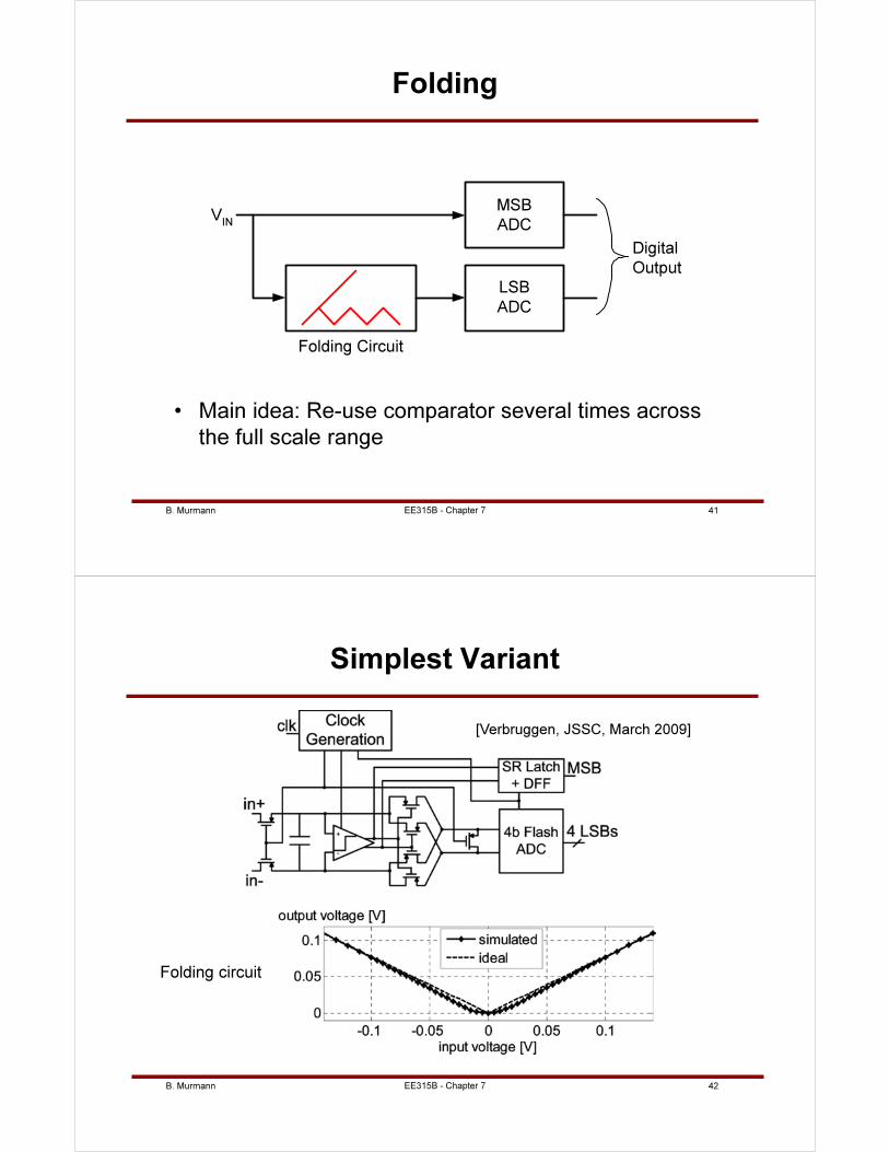
B. Murmann 41EE315B - Chapter 7
Folding
• Main idea: Re-use comparator several times across
the full scale range
LSB
ADC
MSB
ADC
Folding Circuit
VIN
Digital
Output
B. Murmann 42
Simplest Variant
EE315B - Chapter 7
[Verbruggen, JSSC, March 2009]
Folding circuit
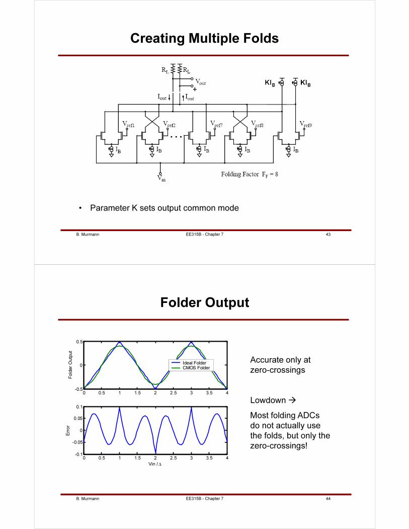
B. Murmann 43EE315B - Chapter 7
Creating Multiple Folds
• Parameter K sets output common mode
B. Murmann 44EE315B - Chapter 7
Folder Output
0 0.5 1 1.5 2 2.5 3 3.5 4-0.5
0
0.5
Fold
er
Outp
ut
0 0.5 1 1.5 2 2.5 3 3.5 4-0.1
-0.05
0
0.05
0.1
Err
or
Vin / ∆
Ideal Folder
CMOS Folder
Accurate only at
zero-crossings
Lowdown
Most folding ADCs
do not actually use
the folds, but only the
zero-crossings!
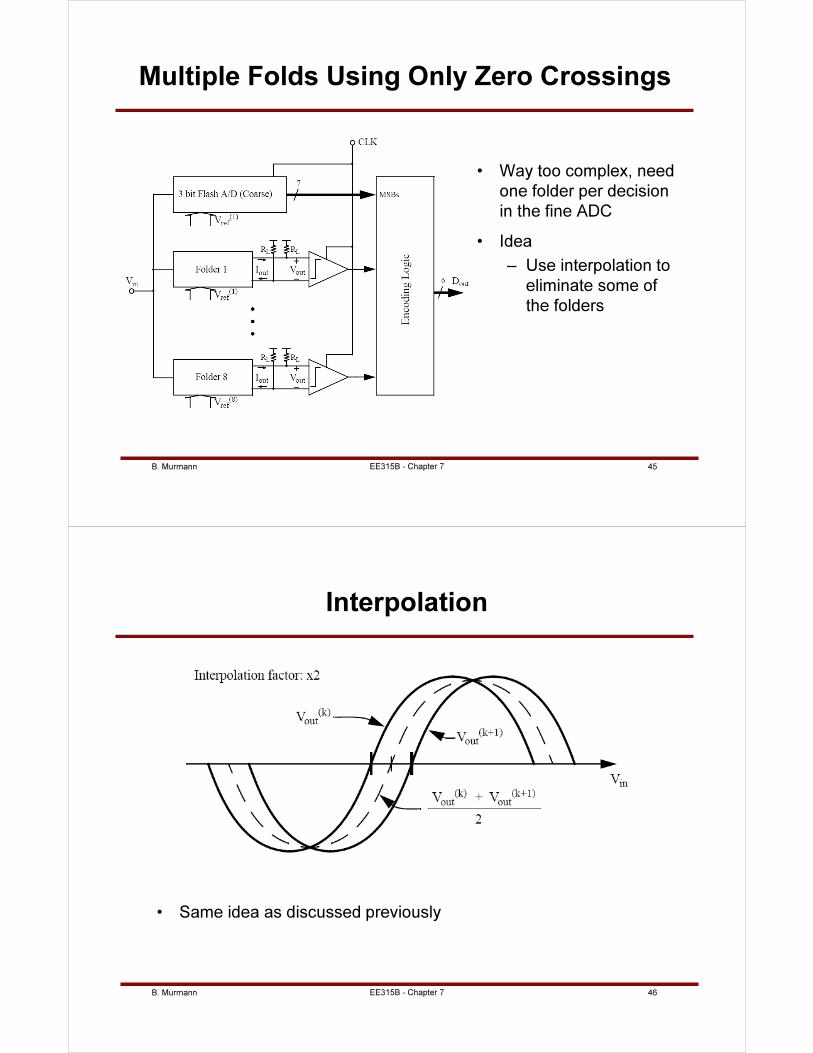
B. Murmann 45EE315B - Chapter 7
Multiple Folds Using Only Zero Crossings
• Way too complex, need
one folder per decision
in the fine ADC
• Idea
– Use interpolation to
eliminate some of
the folders
B. Murmann 46EE315B - Chapter 7
Interpolation
• Same idea as discussed previously
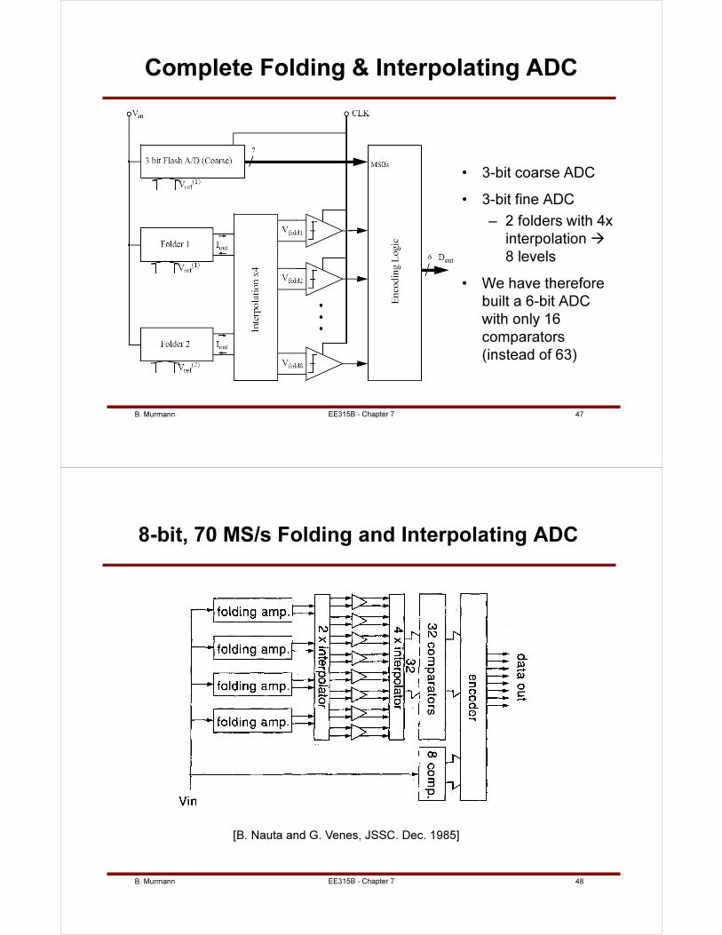
B. Murmann 47EE315B - Chapter 7
Complete Folding & Interpolating ADC
• 3-bit coarse ADC
• 3-bit fine ADC
– 2 folders with 4x
interpolation
8 levels
• We have therefore
built a 6-bit ADC
with only 16
comparators
(instead of 63)
B. Murmann 48
8-bit, 70 MS/s Folding and Interpolating ADC
EE315B - Chapter 7
[B. Nauta and G. Venes, JSSC. Dec. 1985]
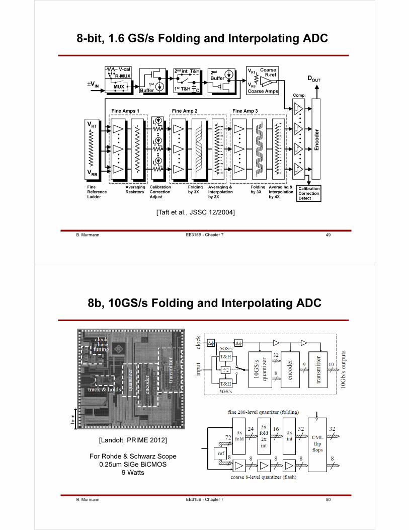
B. Murmann 49EE315B - Chapter 7
8-bit, 1.6 GS/s Folding and Interpolating ADC
[Taft et al., JSSC 12/2004]
B. Murmann 50
8b, 10GS/s Folding and Interpolating ADC
[Landolt, PRIME 2012]
For Rohde & Schwarz Scope
0.25um SiGe BiCMOS
9 Watts
EE315B - Chapter 7
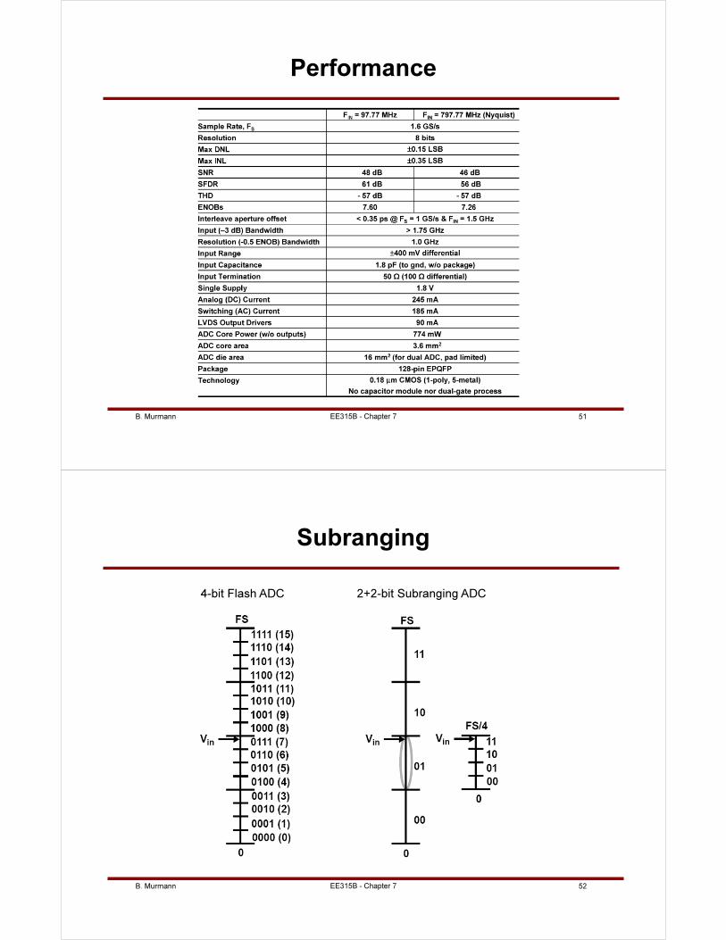
B. Murmann 51EE315B - Chapter 7
Performance
B. Murmann 52
Subranging
EE315B - Chapter 7
4-bit Flash ADC 2+2-bit Subranging ADC
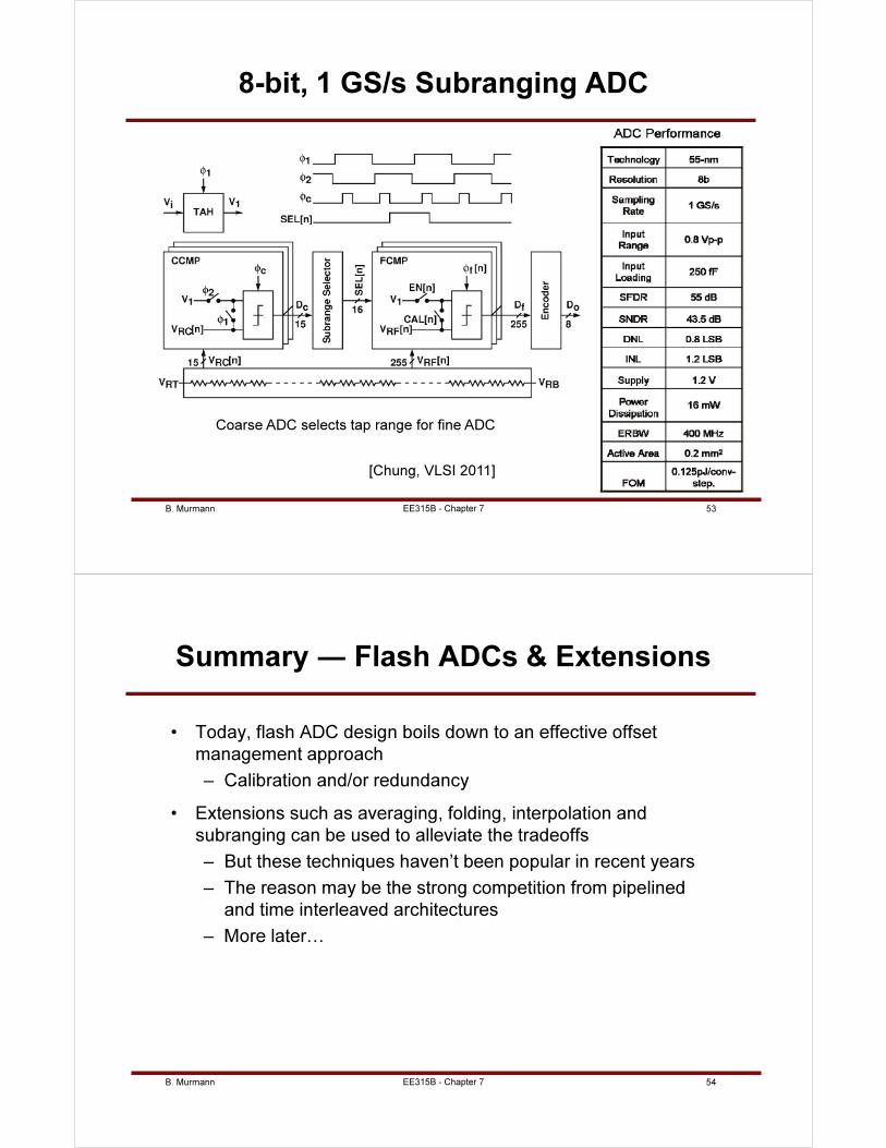
B. Murmann 53
8-bit, 1 GS/s Subranging ADC
EE315B - Chapter 7
[Chung, VLSI 2011]
Coarse ADC selects tap range for fine ADC
B. Murmann 54
Summary ― Flash ADCs & Extensions
• Today, flash ADC design boils down to an effective offset
management approach
– Calibration and/or redundancy
• Extensions such as averaging, folding, interpolation and
subranging can be used to alleviate the tradeoffs
– But these techniques haven’t been popular in recent years
– The reason may be the strong competition from pipelined
and time interleaved architectures
– More later…
EE315B - Chapter 7
B. Murmann 55EE315B - Chapter 7
Selected References (1)
Flash ADCs, Offset Averaging
1. K. Kattmann and J. Barrow, "A Technique for Reducing Differential Non-Linearity
Errors in Flash A/D Converters," ISSCC Digest of Technical Papers, pp. 170-171,
Feb. 1991.
2. K. Bult and A. Buchwald, "An embedded 240-mW 10-b 50-MS/s CMOS ADC in 1-
mm2," IEEE J. of Solid-State Ckts., pp. 1887-1895, Dec. 1997.
3. M. Choi and A. A. Abidi, “A 6 b 1.3 Gsample/s A/D converter in 0.35µm CMOS,” IEEE
J. Solid-State Circuits, pp. 1847–1858, Dec. 2001.
4. C. S. Scholtens and M. Vertregt, “A 6-b 1.6-Gsample/s Flash ADC in 0.18-µm CMOS
Using Averaging Termination,” IEEE J. of Solid-State Ckts., vol. 37, pp. 1599-1609,
Dec. 2002.
5. X. Jiang, M-C. F. Chang, "A 1-GHz signal bandwidth 6-bit CMOS ADC with power-
efficient averaging," IEEE J. of Solid-State Circuits, pp. 532- 535, Feb. 2005.
Folding and Interpolating A/D Converters
6. R.C. Taft et al., "A 1.8-V 1.6-GSample/s 8-b self-calibrating folding ADC with 7.26
ENOB at Nyquist frequency," IEEE J. Solid-State Ckts., pp. 2107-2115 Dec. 2004.
7. B. Nauta and A. G. W. Venes, “A 70-MS/s 110-mW 8-b CMOS Folding and
Interpolating A/D Converter,” IEEE J. of Solid-State Circuits, pp. 1302-1308, Dec.
1995.
B. Murmann 56EE315B - Chapter 7
Selected References (2)
8. M. P. Flynn and B. Sheahan, “A 400-MSample/s, 6-b CMOS Folding and Interpolating ADC,” IEEE J. of Solid-State Circuits, pp. 1932-1938, Dec. 1998.
9. H. Pan, M. Segami, M. Choi, J. Cao, F. Hatori and A. Abidi, “A 3.3V, 12b, 50MSample/s A/D converter in 0.6mm CMOS with over 80dB SFDR,” ISSCC Digest of Technical Papers, pp. 40-41, Feb. 2000.
10. M.-J. Choe, B.-S. Song and K. Bacrania, “A 13b 40MSample/s CMOS pipelined folding ADC with background offset trimming,” ISSCC Digest of Technical Papers, pp. 36-37, Feb. 2000.
11. G. Hoogzaad and R. Roovers, “A 65-mW, 10-bit, 40-Msample/s BiCMOS Nyquist ADC in 0.8 mm2,” IEEE J. Solid-State Circuits, pp. 1796-1802, Dec. 1999.
12. K. Nagaraj, F. Chen, T. Le and T. R. Viswanathan, “Efficient 6-bit A/D converter using a 1-bit folding front end,” IEEE J. Solid-State Circuits, pp. 1056-1062, Aug. 1999.
13. M.-J. Choe and B.-S. Song, “An 8b 100MSample/s CMOS pipelined folding ADC,” VLSI Symposium Digest of Technical Papers, pp. 81-82, Jun. 1999.
14. K. Bult and A. Buchwald, “An embedded 240-mW 10-b 50-MS/s CMOS ADC in 1 mm2,” IEEE J. Solid-State Circuits, vol. 32, pp. 1887-1895, Dec. 1997.
15. P. Vorenkamp and R. Roovers, “A 12-b, 60-MSample/s cascaded folding and interpolating ADC,” IEEE J. Solid-State Circuits, vol. 32, pp. 1876-1886, Dec. 1997.
16. A. G. W. Venes and R. J. van de Plassche, “An 80-MHz, 8-b CMOS folding A/D converter with distributed track-and-hold preprocessing,” IEEE J. Solid-State Circuits, vol. 31, pp. 1846-1853, Dec. 1996.
B. Murmann 57EE315B - Chapter 7
Selected References (3)
17. M. P. Flynn and D. J. Allstot, “CMOS folding A/D converters with current-mode
interpolation,” IEEE J. Solid-State Circuits, vol. 31, pp. 1248-1257, Dec. 1996.
18. R. Roovers and M. S. J. Steyaert, “A 175 Ms/s, 6 b, 160 mW, 3.3 V CMOS A/D
converter,” IEEE J. Solid-State Circuits, vol. 31, pp. 938-944, Jul. 1996.
19. W. T. Colleran and A. A. Abidi, “A 10-b, 75-MHz two-stage pipelined bipolar A/D
converter,” IEEE J. Solid-State Circuits, vol. 28, pp. 1187-1199, Dec. 1993.
20. J. van Valburg and R. J. van de Plassche, “An 8-b 650-MHz folding ADC,” IEEE J.
Solid-State Circuits, vol. 27, pp. 1662-1666, Dec. 1992.
21. R. J. van de Plassche and P. Baltus, “An 8-bit 100-MHz full-Nyquist analog-to-digital
converter,” IEEE J. Solid-State Circuits, vol. 23, pp. 1334-1344, Dec. 1988.
22. R. E. J. Van de Grift, I. W. J. M. Rutten and M. van der Veen, “An 8-bit video ADC
incorporating folding and interpolation techniques,” IEEE J. Solid-State Circuits, vol.
SC-22, pp. 944-953, Dec. 1987.
23. R. E. J. van de Grift and R. J. van de Plassche, “A monolithic 8-bit video A/D
converter,” IEEE J. Solid-State Circuits, vol. SC-19, pp. 374-378, Jun. 1984.
24. R.C. Taft, et al., "A 1.8V 1.0GS/s 10b self-calibrating unified-folding-interpolating
ADC with 9.1 ENOB at Nyquist frequency," ISSCC Digest of Technical Papers,
pp.78-79, 79a, Feb. 2009.
B. Murmann 1EE315B - Chapter 8
SAR ADCs
Boris Murmann
Stanford University
Copyright © 2013 by Boris Murmann
B. Murmann 2
Similarity Between Non-Flash ADC
Architectures
• Most ADC architectures (other than flash) are based on minimizing
the error between input and a D/A signal approximation
– SAR ADC uses comparator to sense ε
– Sigma-delta ADC minimizes ε via integration and feedback
– Pipeline uses distributed DAC
D/A
MinimizeΣ
Vinε
Dout
-
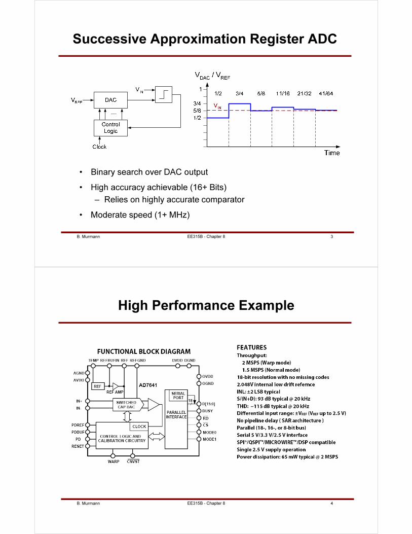
B. Murmann 3EE315B - Chapter 8
Successive Approximation Register ADC
• Binary search over DAC output
• High accuracy achievable (16+ Bits)
– Relies on highly accurate comparator
• Moderate speed (1+ MHz)
B. Murmann 4EE315B - Chapter 8
High Performance Example
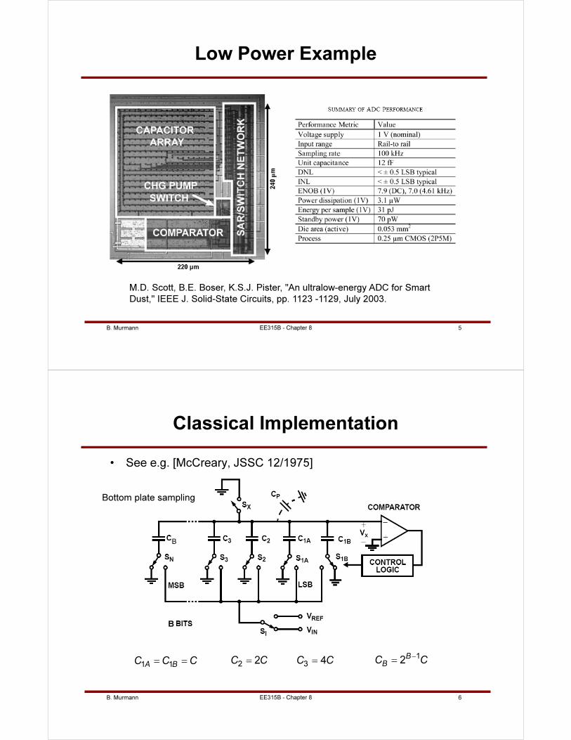
B. Murmann 5EE315B - Chapter 8
Low Power Example
M.D. Scott, B.E. Boser, K.S.J. Pister, "An ultralow-energy ADC for Smart
Dust," IEEE J. Solid-State Circuits, pp. 1123 -1129, July 2003.
B. Murmann 6EE315B - Chapter 8
Classical Implementation
• See e.g. [McCreary, JSSC 12/1975]
1 1A BC C C= = 2 2C C= 3 4C C=1
2B
BC C−
=
B
B
Bottom plate sampling
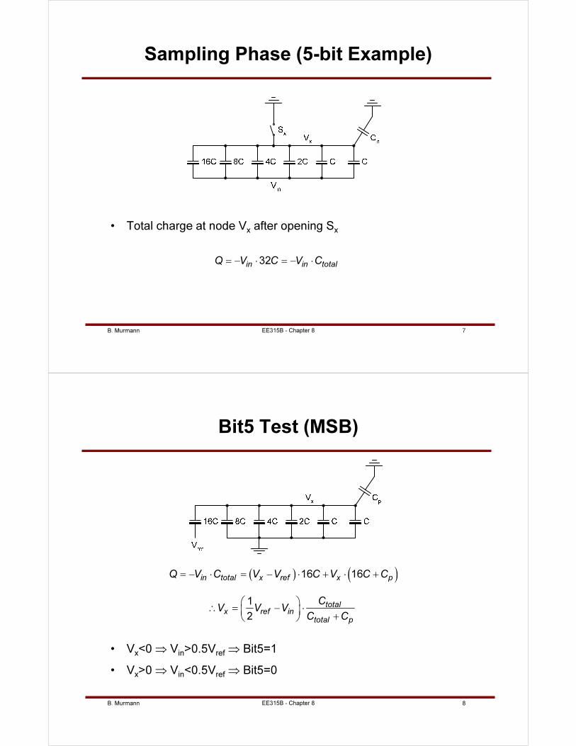
B. Murmann 7EE315B - Chapter 8
Sampling Phase (5-bit Example)
• Total charge at node Vx
after opening Sx
32in in totalQ V C V C= − ⋅ = − ⋅
B. Murmann 8EE315B - Chapter 8
Bit5 Test (MSB)
• Vx<0 ⇒ V
in>0.5V
ref⇒ Bit5=1
• Vx>0 ⇒ V
in<0.5V
ref⇒ Bit5=0
( ) ( )16 16in total x ref x pQ V C V V C V C C= − ⋅ = − ⋅ + ⋅ +
1
2
totalx ref in
total p
CV V V
C C
∴ = − ⋅
+
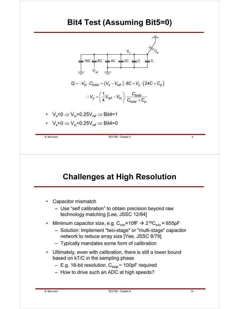
B. Murmann 9EE315B - Chapter 8
Bit4 Test (Assuming Bit5=0)
• Vx<0 ⇒ V
in>0.25V
ref⇒ Bit4=1
• Vx>0 ⇒ V
in<0.25V
ref⇒ Bit4=0
( ) ( )8 24in total x ref x pQ V C V V C V C C= − ⋅ = − ⋅ + ⋅ +
1
4
totalx ref in
total p
CV V V
C C
∴ = − ⋅
+
B. Murmann 10EE315B - Chapter 8
Challenges at High Resolution
• Capacitor mismatch
– Use “self calibration” to obtain precision beyond raw
technology matching [Lee, JSSC 12/84]
• Minimum capacitor size, e.g. Cmin
=10fF 216Cmin
= 655pF
– Solution: Implement "two-stage" or "multi-stage" capacitor
network to reduce array size [Yee, JSSC 8/79]
– Typically mandates some form of calibration
• Ultimately, even with calibration, there is still a lower bound
based on kT/C in the sampling phase
– E.g. 16-bit resolution, Ctotal
~ 100pF required
– How to drive such an ADC at high speeds?
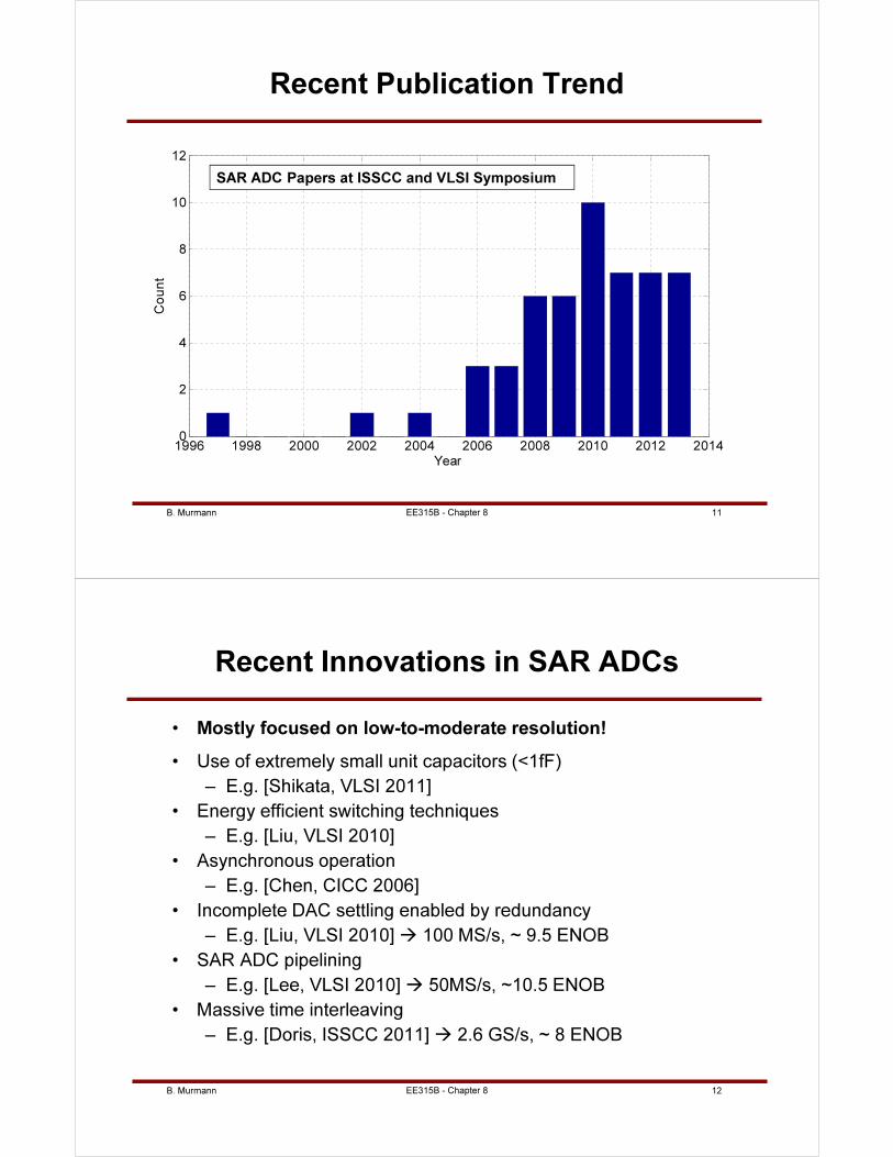
B. Murmann 11
Recent Publication Trend
EE315B - Chapter 8
1996 1998 2000 2002 2004 2006 2008 2010 2012 20140
2
4
6
8
10
12
Year
Count
SAR ADC Papers at ISSCC and VLSI Symposium
B. Murmann 12
Recent Innovations in SAR ADCs
• Mostly focused on low-to-moderate resolution!
• Use of extremely small unit capacitors (<1fF)
– E.g. [Shikata, VLSI 2011]
• Energy efficient switching techniques
– E.g. [Liu, VLSI 2010]
• Asynchronous operation
– E.g. [Chen, CICC 2006]
• Incomplete DAC settling enabled by redundancy
– E.g. [Liu, VLSI 2010] 100 MS/s, ~ 9.5 ENOB
• SAR ADC pipelining
– E.g. [Lee, VLSI 2010] 50MS/s, ~10.5 ENOB
• Massive time interleaving
– E.g. [Doris, ISSCC 2011] 2.6 GS/s, ~ 8 ENOB
EE315B - Chapter 8
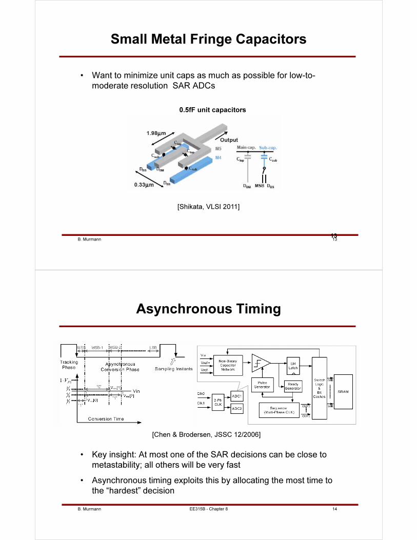
B. Murmann 13
Small Metal Fringe Capacitors
• Want to minimize unit caps as much as possible for low-to-
moderate resolution SAR ADCs
13
[Shikata, VLSI 2011]
0.5fF unit capacitors
B. Murmann 14
Asynchronous Timing
• Key insight: At most one of the SAR decisions can be close to
metastability; all others will be very fast
• Asynchronous timing exploits this by allocating the most time to
the “hardest” decision
[Chen & Brodersen, JSSC 12/2006]
EE315B - Chapter 8
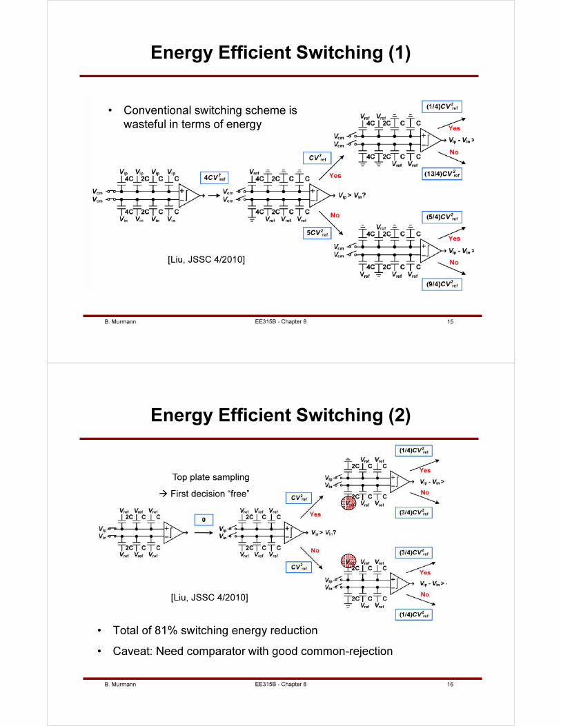
B. Murmann 15
Energy Efficient Switching (1)
[Liu, JSSC 4/2010]
• Conventional switching scheme is
wasteful in terms of energy
[Liu, JSSC 4/2010]
EE315B - Chapter 8
B. Murmann 16
Energy Efficient Switching (2)
• Total of 81% switching energy reduction
• Caveat: Need comparator with good common-rejection
Top plate sampling
First decision “free”
[Liu, JSSC 4/2010]
EE315B - Chapter 8
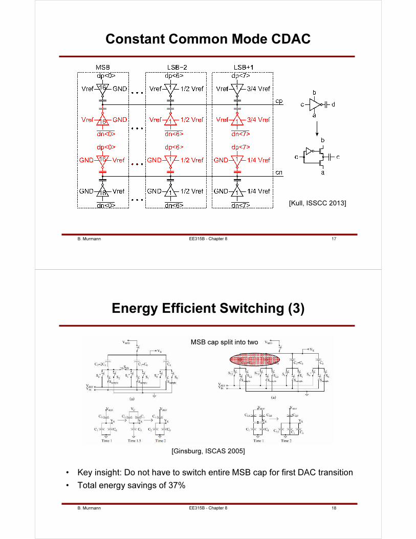
B. Murmann 17
Constant Common Mode CDAC
[Kull, ISSCC 2013]
EE315B - Chapter 8
B. Murmann 18
Energy Efficient Switching (3)
• Key insight: Do not have to switch entire MSB cap for first DAC transition
• Total energy savings of 37%
[Ginsburg, ISCAS 2005]
MSB cap split into two
EE315B - Chapter 8
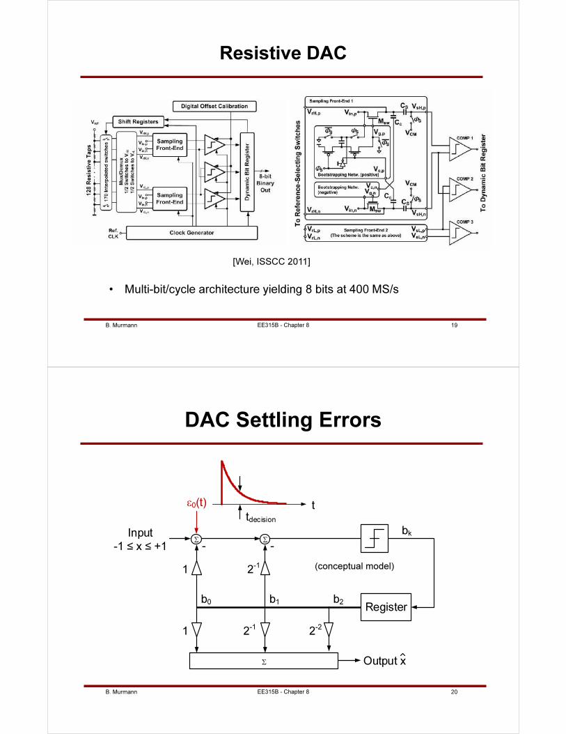
B. Murmann 19
Resistive DAC
• Multi-bit/cycle architecture yielding 8 bits at 400 MS/s
[Wei, ISSCC 2011]
EE315B - Chapter 8
B. Murmann 20
DAC Settling Errors
1
Σ
b2
ΣInput
-1 ≤ x ≤ +1
Register
bk
b0 b1
- -
Output x
2-1
2-1 2-21
Σ
ε0(t) ttdecision
(conceptual model)
EE315B - Chapter 8
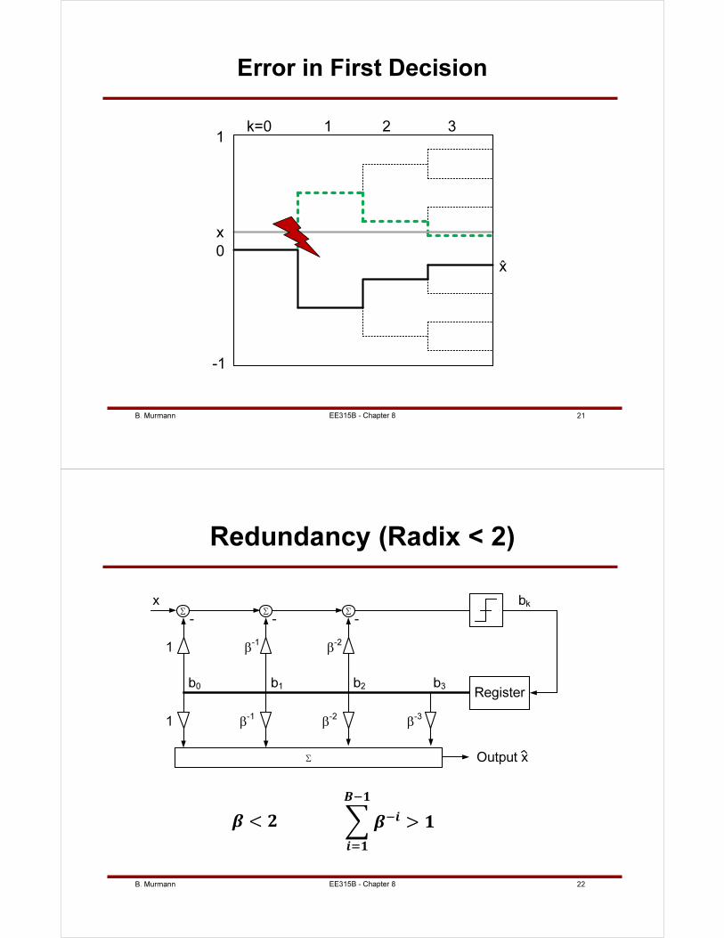
B. Murmann 21
0
1
-1
k=0 2 3
x
x
1
Error in First Decision
EE315B - Chapter 8
B. Murmann 22
Redundancy (Radix < 2)
1
Σ Σ
b3
Σ
x
Register
bk
b0 b1 b2
- - -
Output x
β-1
β-2
β-1
β-2
β-3
1
Σ
< >
EE315B - Chapter 8
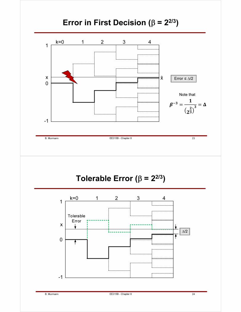
B. Murmann 23
0
1
-1
k=0 2 3
xx
1 4
Error in First Decision (β = 22/3)
Error ≤ ∆/2
Note that
EE315B - Chapter 8
B. Murmann 24
0
1
-1
k=0 2 3
x
1 4
Tolerable
Error
Tolerable Error (β = 22/3)
∆/2
EE315B - Chapter 8
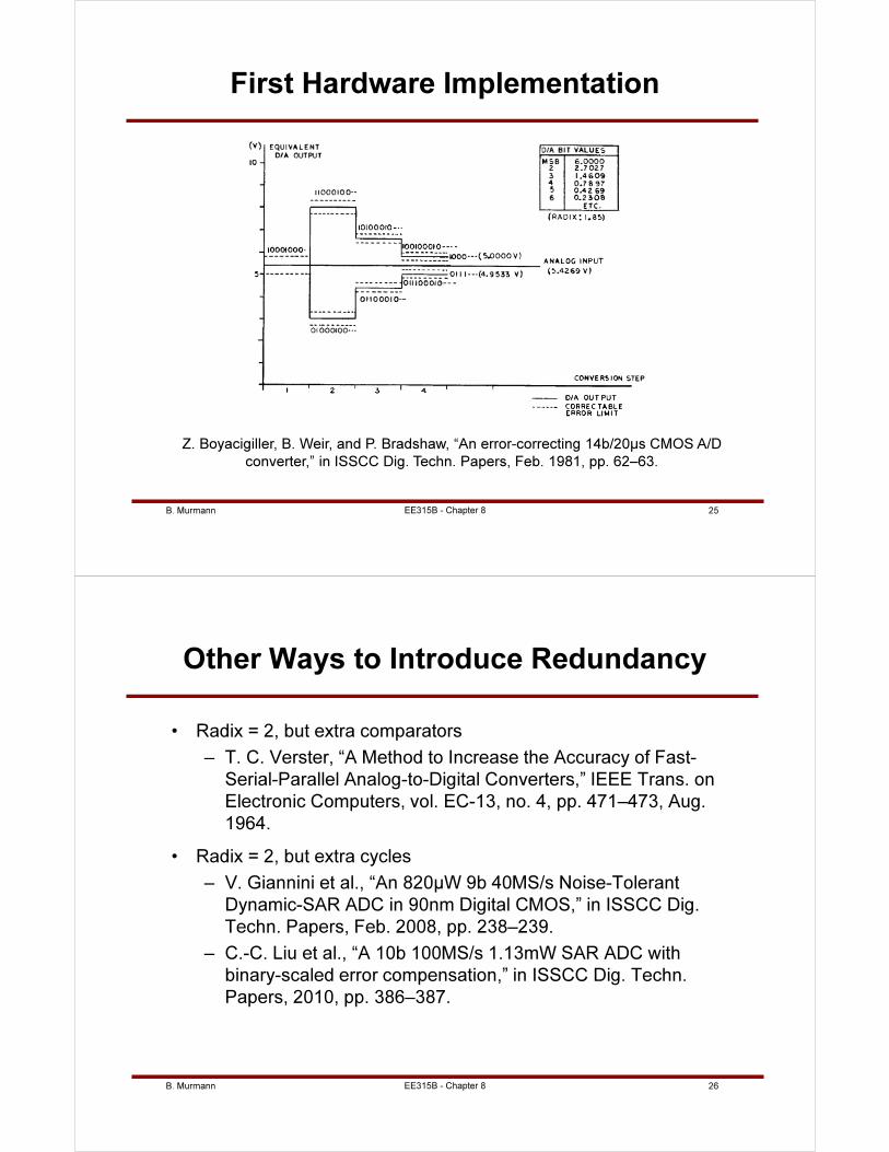
B. Murmann 25
First Hardware Implementation
Z. Boyacigiller, B. Weir, and P. Bradshaw, “An error-correcting 14b/20µs CMOS A/D
converter,” in ISSCC Dig. Techn. Papers, Feb. 1981, pp. 62–63.
EE315B - Chapter 8
B. Murmann 26
Other Ways to Introduce Redundancy
• Radix = 2, but extra comparators
– T. C. Verster, “A Method to Increase the Accuracy of Fast-
Serial-Parallel Analog-to-Digital Converters,” IEEE Trans. on
Electronic Computers, vol. EC-13, no. 4, pp. 471–473, Aug.
1964.
• Radix = 2, but extra cycles
– V. Giannini et al., “An 820μW 9b 40MS/s Noise-Tolerant
Dynamic-SAR ADC in 90nm Digital CMOS,” in ISSCC Dig.
Techn. Papers, Feb. 2008, pp. 238–239.
– C.-C. Liu et al., “A 10b 100MS/s 1.13mW SAR ADC with
binary-scaled error compensation,” in ISSCC Dig. Techn.
Papers, 2010, pp. 386–387.
EE315B - Chapter 8
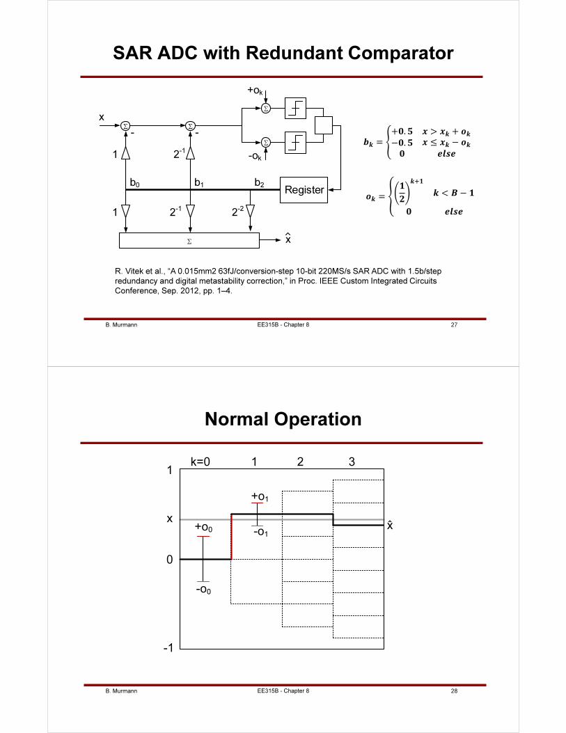
B. Murmann 27
SAR ADC with Redundant Comparator
1
Σ
b2
Σ
x
Registerb0 b1
- -
x
2-1
2-1
2-2
1
Σ
Σ
Σ
-ok
+ok
= +. > + −. ≤ −
= < −
R. Vitek et al., “A 0.015mm2 63fJ/conversion-step 10-bit 220MS/s SAR ADC with 1.5b/step
redundancy and digital metastability correction,” in Proc. IEEE Custom Integrated Circuits
Conference, Sep. 2012, pp. 1–4.
EE315B - Chapter 8
B. Murmann 28
Normal Operation
0
1
-1
k=0 2 3
xx
1
+o0
-o0
+o1
-o1
EE315B - Chapter 8
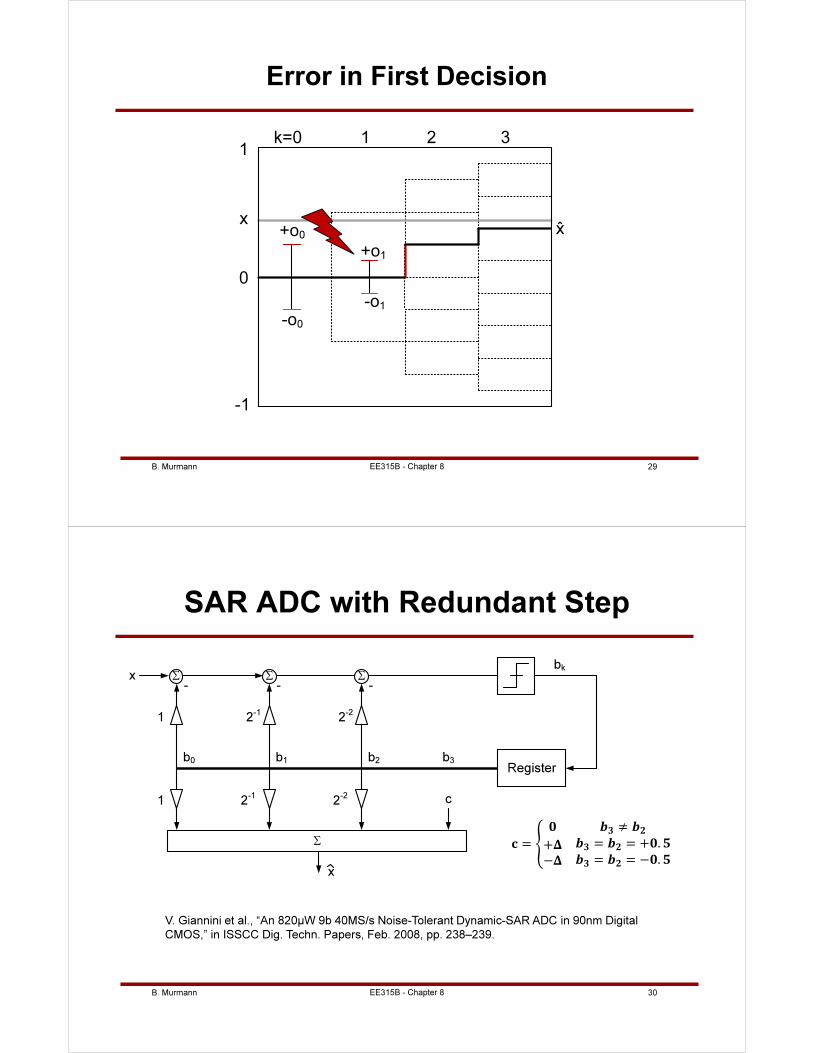
B. Murmann 29
Error in First Decision
0
1
-1
k=0 2 3
xx
1
+o0
-o0
+o1
-o1
EE315B - Chapter 8
B. Murmann 30
SAR ADC with Redundant Step
V. Giannini et al., “An 820μW 9b 40MS/s Noise-Tolerant Dynamic-SAR ADC in 90nm Digital
CMOS,” in ISSCC Dig. Techn. Papers, Feb. 2008, pp. 238–239.
1
ΣΣx
Register
bk
b0 b1
- -
x
2-1
2-1
1
Σ
Σ
b2
-
2-2
2-2 c
b3
= ≠
+− = = +. = = −.
EE315B - Chapter 8
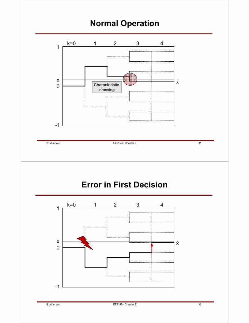
B. Murmann 31
0
1
-1
k=0 2 3
xx
1 4
Normal Operation
Characteristic
crossing
EE315B - Chapter 8
B. Murmann 32
0
1
-1
k=0 2 3
xx
1 4
Error in First Decision
EE315B - Chapter 8
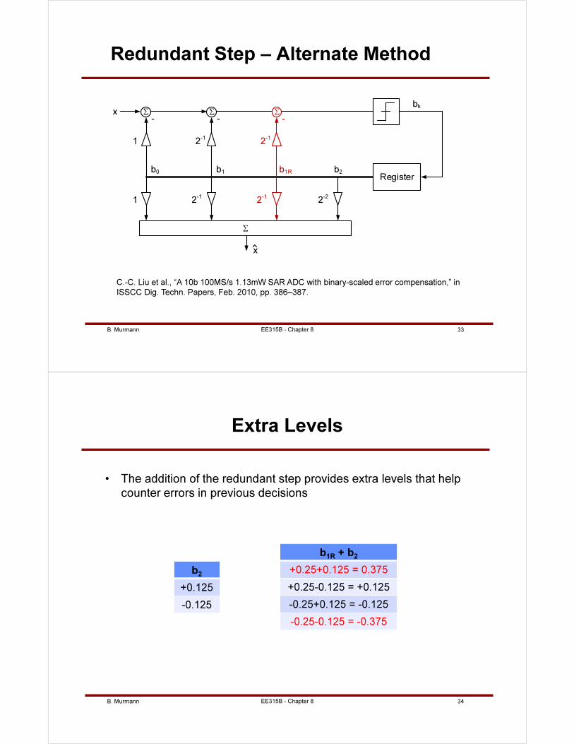
B. Murmann 33
Redundant Step – Alternate Method
C.-C. Liu et al., “A 10b 100MS/s 1.13mW SAR ADC with binary-scaled error compensation,” in
ISSCC Dig. Techn. Papers, Feb. 2010, pp. 386–387.
1
ΣΣx
Register
bk
b0 b1
- -
x
2-1
2-1
1
Σ
Σ
b1R
-
2-1
2-1
b2
2-2
EE315B - Chapter 8
B. Murmann 34
Extra Levels
• The addition of the redundant step provides extra levels that help
counter errors in previous decisions
b2
+0.125
-0.125
b1R
+ b2
+0.25+0.125 = 0.375
+0.25-0.125 = +0.125
-0.25+0.125 = -0.125
-0.25-0.125 = -0.375
EE315B - Chapter 8
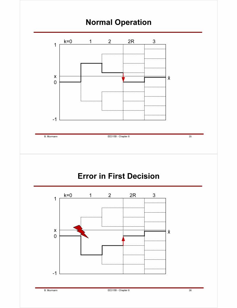
B. Murmann 35
0
1
-1
k=0 2 2R
xx
1 3
Normal Operation
EE315B - Chapter 8
B. Murmann 36
0
1
-1
k=0 2 2R
xx
1 3
Error in First Decision
EE315B - Chapter 8
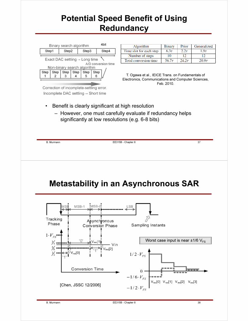
B. Murmann 37
Potential Speed Benefit of Using
Redundancy
• Benefit is clearly significant at high resolution
– However, one must carefully evaluate if redundancy helps
significantly at low resolutions (e.g. 6-8 bits)
T. Ogawa et al., IEICE Trans. on Fundamentals of
Electronics, Communications and Computer Sciences,
Feb. 2010.
EE315B - Chapter 8
B. Murmann 38
Metastability in an Asynchronous SAR
[Chen, JSSC 12/2006]
Worst case input is near ±1/6 VFS
EE315B - Chapter 8
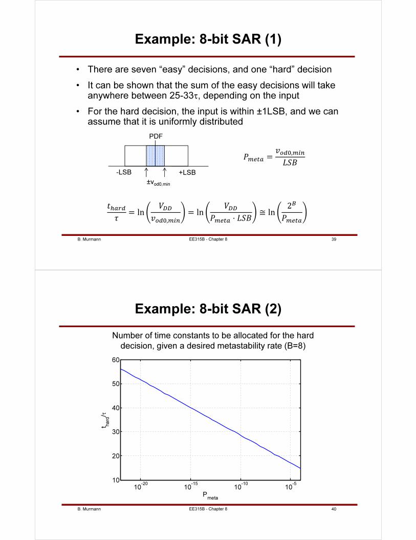
B. Murmann 39
Example: 8-bit SAR (1)
• There are seven “easy” decisions, and one “hard” decision
• It can be shown that the sum of the easy decisions will take anywhere between 25-33τ, depending on the input
• For the hard decision, the input is within ±1LSB, and we can assume that it is uniformly distributed
+LSB-LSB
±vod0,min
=,
= ln
,
= ln
⋅ ≅ ln
2
EE315B - Chapter 8
B. Murmann 40
Example: 8-bit SAR (2)
Number of time constants to be allocated for the hard
decision, given a desired metastability rate (B=8)
10-20
10-15
10-10
10-5
10
20
30
40
50
60
Pmeta
t hard/τ
EE315B - Chapter 8
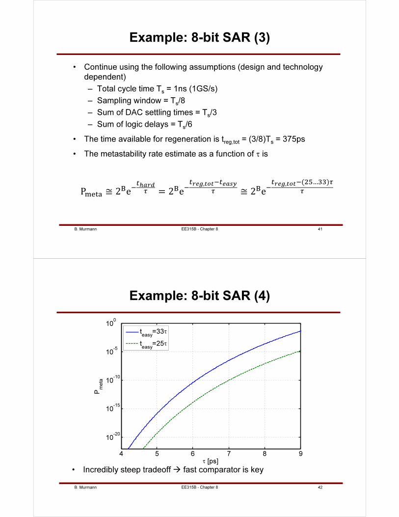
B. Murmann 41
Example: 8-bit SAR (3)
• Continue using the following assumptions (design and technology
dependent)
– Total cycle time Ts = 1ns (1GS/s)
– Sampling window = Ts/8
– Sum of DAC settling times = Ts/3
– Sum of logic delays = Ts/6
• The time available for regeneration is treg,tot = (3/8)Ts = 375ps
• The metastability rate estimate as a function of τ is
P ≅ 2e
= 2e,
≅ 2e,( …)
EE315B - Chapter 8
B. Murmann 42
Example: 8-bit SAR (4)
• Incredibly steep tradeoff fast comparator is key
4 5 6 7 8 9
10-20
10-15
10-10
10-5
100
Pmeta
τ [ps]
teasy
=33τ
teasy
=25τ
EE315B - Chapter 8
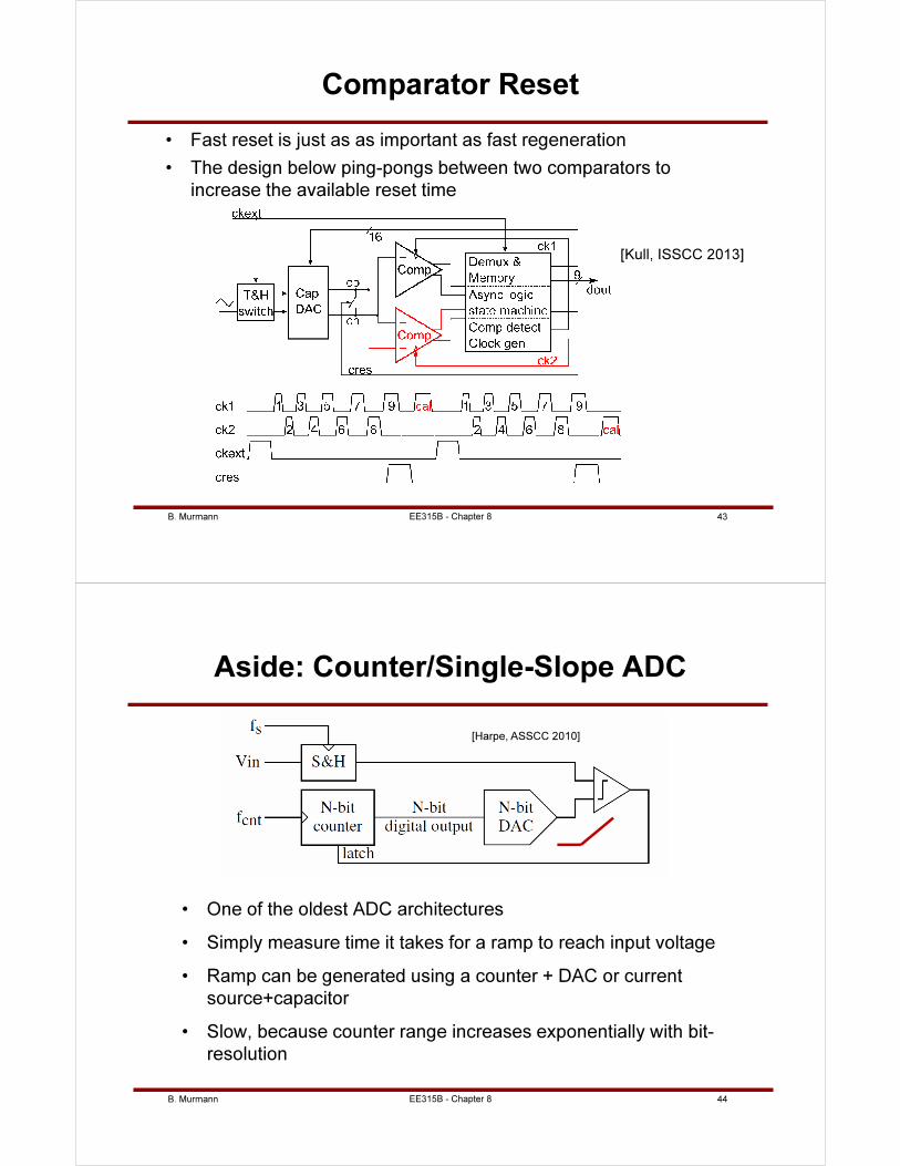
B. Murmann 43
Comparator Reset
• Fast reset is just as as important as fast regeneration
• The design below ping-pongs between two comparators to
increase the available reset time
[Kull, ISSCC 2013]
EE315B - Chapter 8
B. Murmann 44
Aside: Counter/Single-Slope ADC
• One of the oldest ADC architectures
• Simply measure time it takes for a ramp to reach input voltage
• Ramp can be generated using a counter + DAC or current
source+capacitor
• Slow, because counter range increases exponentially with bit-
resolution
[Harpe, ASSCC 2010]
EE315B - Chapter 8

B. Murmann 1
Pipeline ADCs
Boris Murmann
Stanford University
Copyright © 2013 by Boris Murmann
EE315B - Chapter 9
B. Murmann 2
Outline
• Background
– History and state-of the art performance
– Derivation from SAR architecture
• Pipeline ADC basics
– Ideal block diagram and operation, impact of block nonidealities
• Ways to deal with nonidealities
– Redundancy, calibration
• CMOS implementation details
– Stage scaling, MDAC design
• Architectural options
– OTA sharing, SHA-less front-end
• Research topics
EE315B - Chapter 9
B. Murmann 3
Pipeline ADCs – An Old Idea (1956)
B.D. Smith, “An Unusual Electronic Analog-Digital Conversion Method,” IRE Transactions on
Instrumentation, vol. PGI-5, pp. 155-160, June 1956.
EE315B - Chapter 9
B. Murmann 4
Today’s Pipeline ADC Performance Range
Data: http://www.stanford.edu/~murmann/adcsurvey.html
20 30 40 50 60 70 80 90 100 110 12010
4
106
108
1010
SNDRhf
[dB]
f in,hf [
Hz]
Flash
Folding
Two-Step
Pipeline
∆Σ
SAR
Other
1000fsrms
Jitter
100fsrms
Jitter
EE315B - Chapter 9
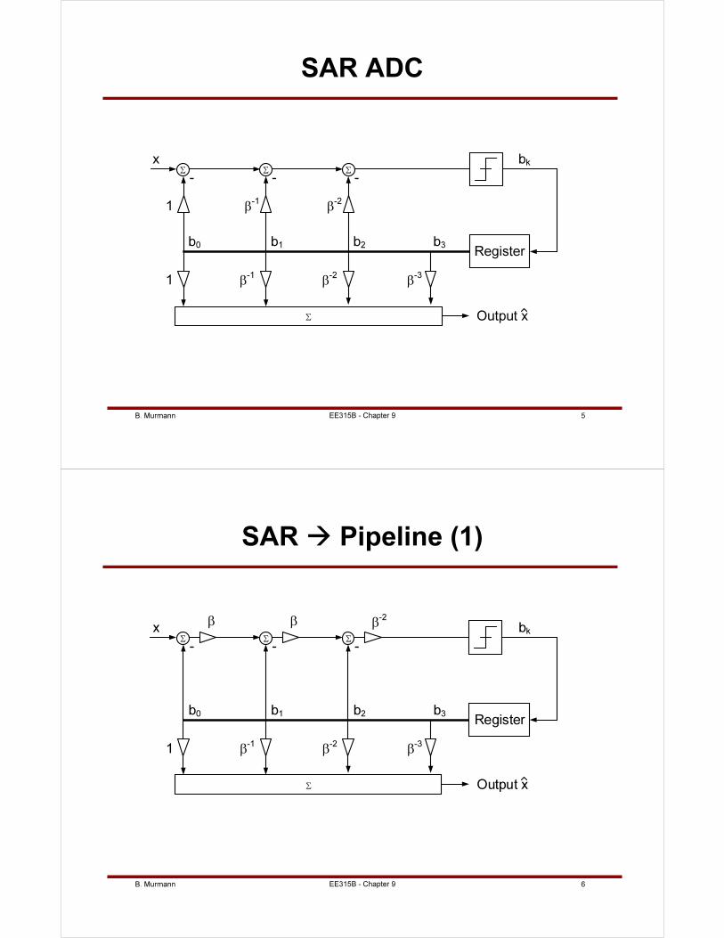
B. Murmann 5
SAR ADC
1
Σ Σ
b3
Σ
x
Register
bk
b0 b1 b2
- - -
Output x
β-1
β-2
β-1
β-2
β-3
1
Σ
EE315B - Chapter 9
B. Murmann 6
SAR Pipeline (1)
Σ Σ
b3
Σ
x
Register
bk
b0 b1 b2
- - -
Output x
β-1
β-2
β-31
Σ
β-2ββ
EE315B - Chapter 9
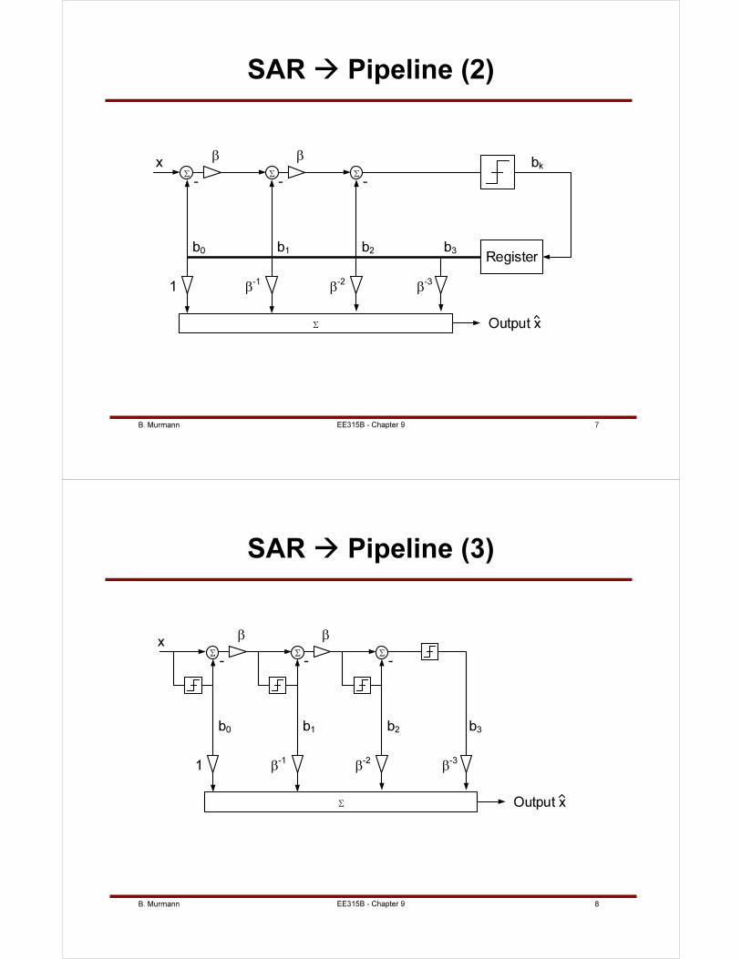
B. Murmann 7
SAR Pipeline (2)
Σ Σ
b3
Σ
x
Register
bk
b0 b1 b2
- - -
Output x
β-1
β-2
β-31
Σ
ββ
EE315B - Chapter 9
B. Murmann 8
SAR Pipeline (3)
Σ Σ
b3
Σ
x
b0 b1 b2
- - -
Output x
β-1
β-2
β-3
1
Σ
ββ
EE315B - Chapter 9
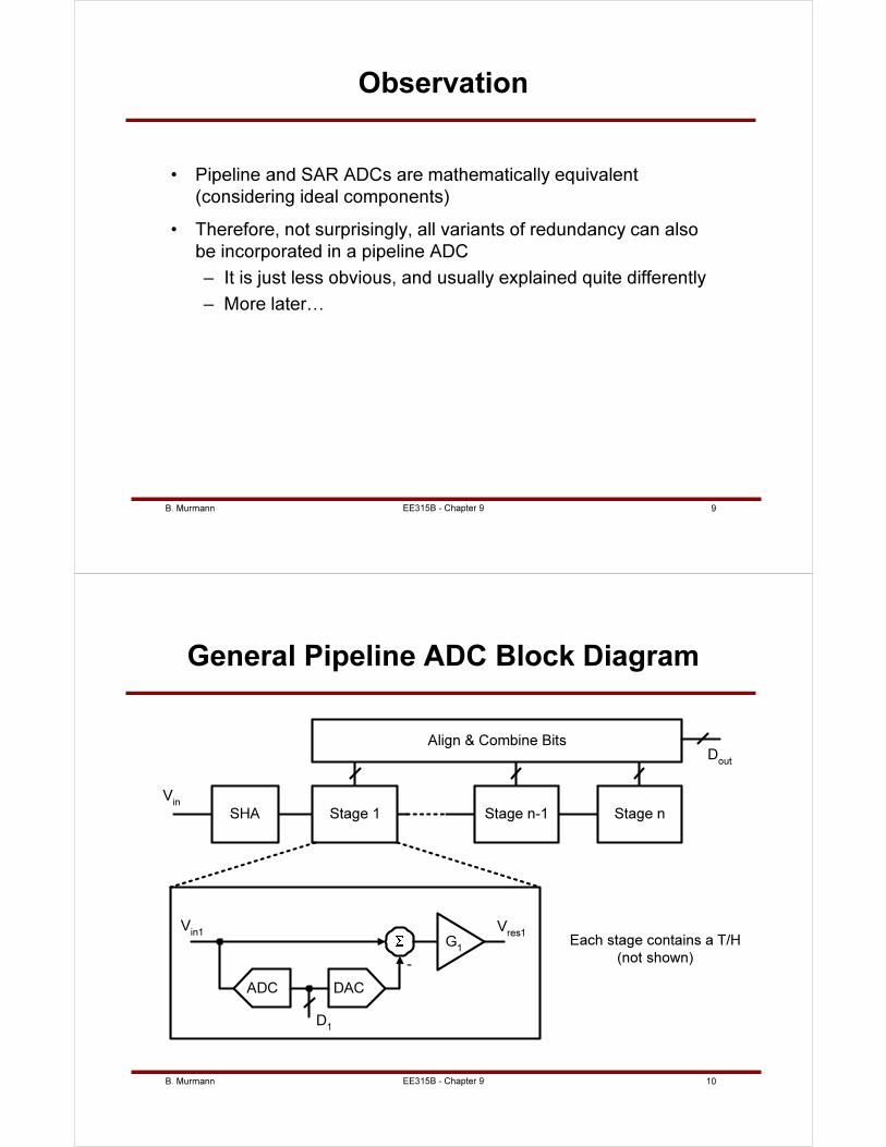
B. Murmann 9
Observation
• Pipeline and SAR ADCs are mathematically equivalent
(considering ideal components)
• Therefore, not surprisingly, all variants of redundancy can also
be incorporated in a pipeline ADC
– It is just less obvious, and usually explained quite differently
– More later…
EE315B - Chapter 9
B. Murmann 10
General Pipeline ADC Block Diagram
ADC DAC
-
D1
Vres1
Vin1
Stage 1 Stage n-1 Stage nSHA
Vin
G1
Align & Combine BitsD
out
G1
Each stage contains a T/H
(not shown)
EE315B - Chapter 9
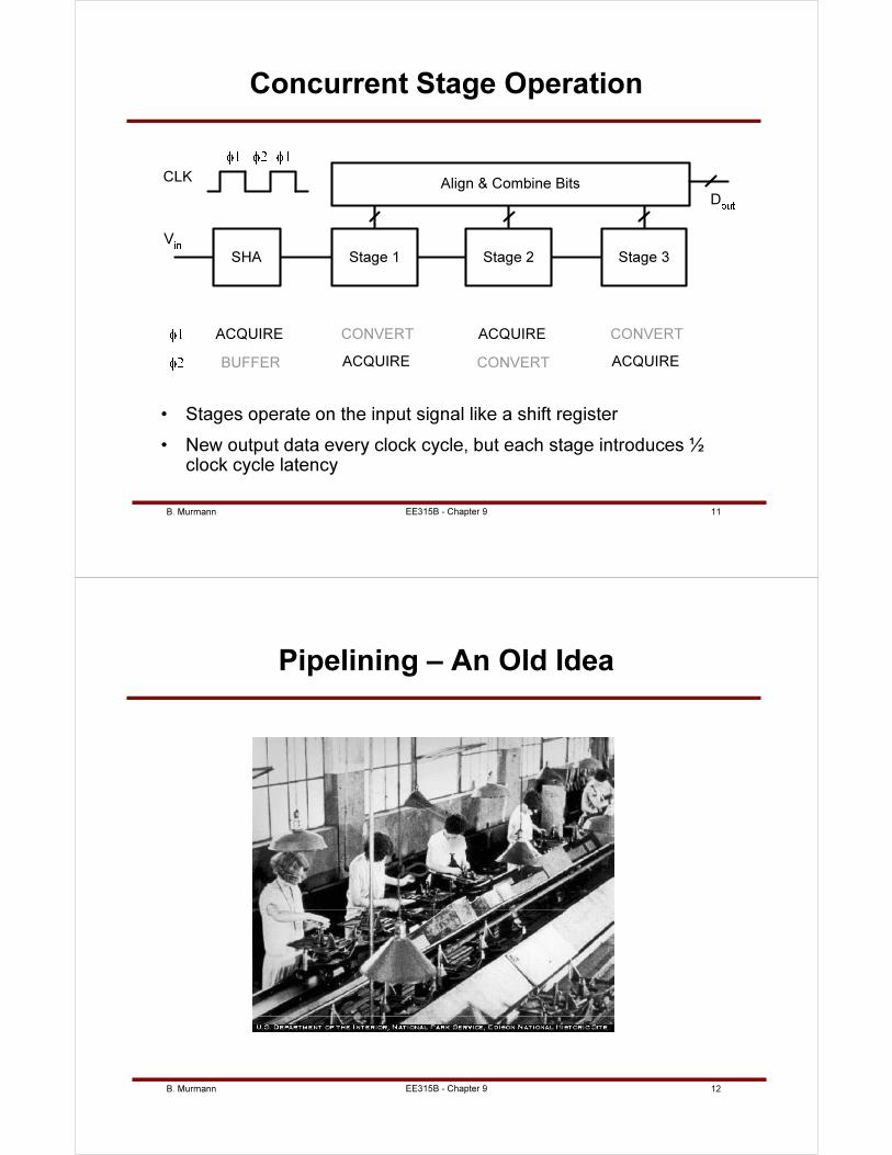
B. Murmann 11
Concurrent Stage Operation
Stage 1 Stage 2 Stage 3SHA
V
Align & Combine BitsD
ACQUIRE
BUFFER
ACQUIRE
CONVERTACQUIRE
CONVERT
ACQUIRE
CONVERT
CLK
• Stages operate on the input signal like a shift register
• New output data every clock cycle, but each stage introduces ½ clock cycle latency
EE315B - Chapter 9
B. Murmann 12
Pipelining – An Old Idea
EE315B - Chapter 9
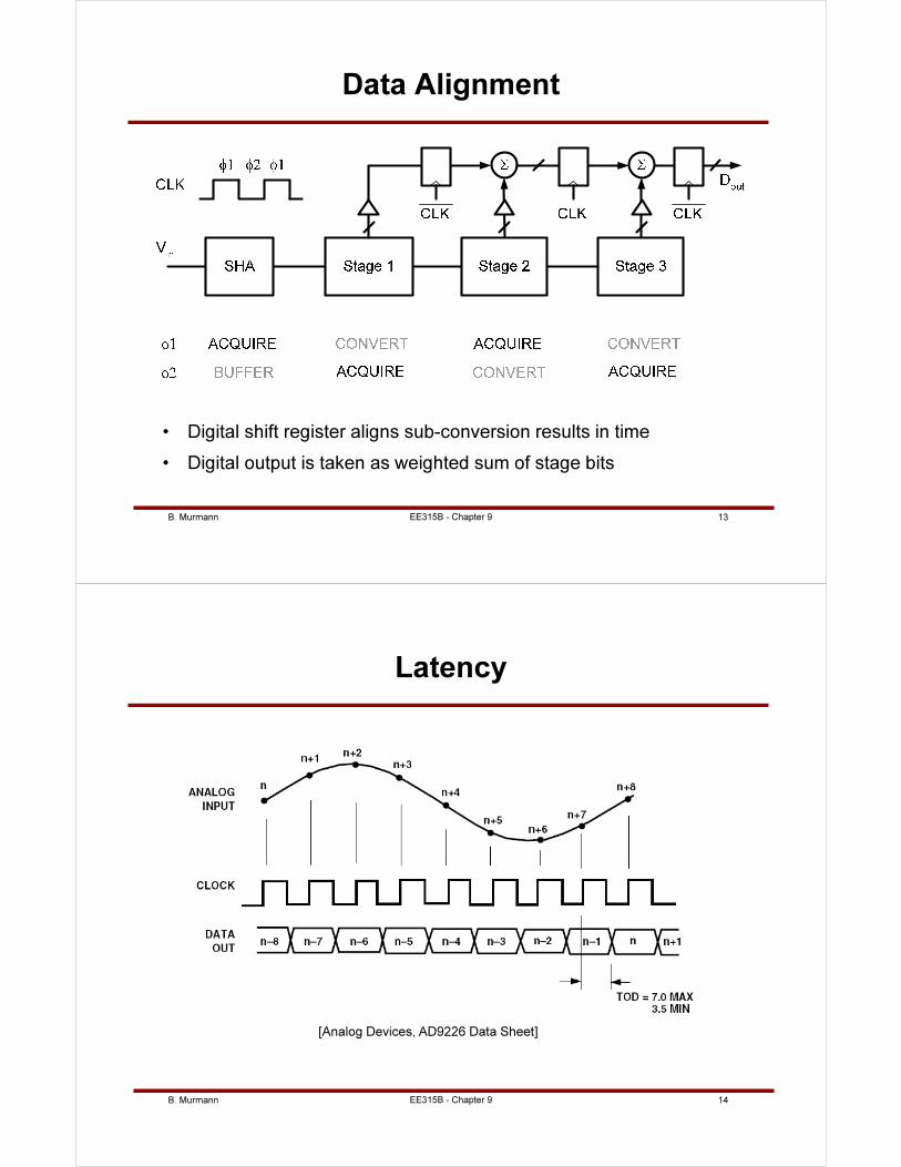
B. Murmann 13
Data Alignment
• Digital shift register aligns sub-conversion results in time
• Digital output is taken as weighted sum of stage bits
EE315B - Chapter 9
B. Murmann 14
Latency
[Analog Devices, AD9226 Data Sheet]
EE315B - Chapter 9
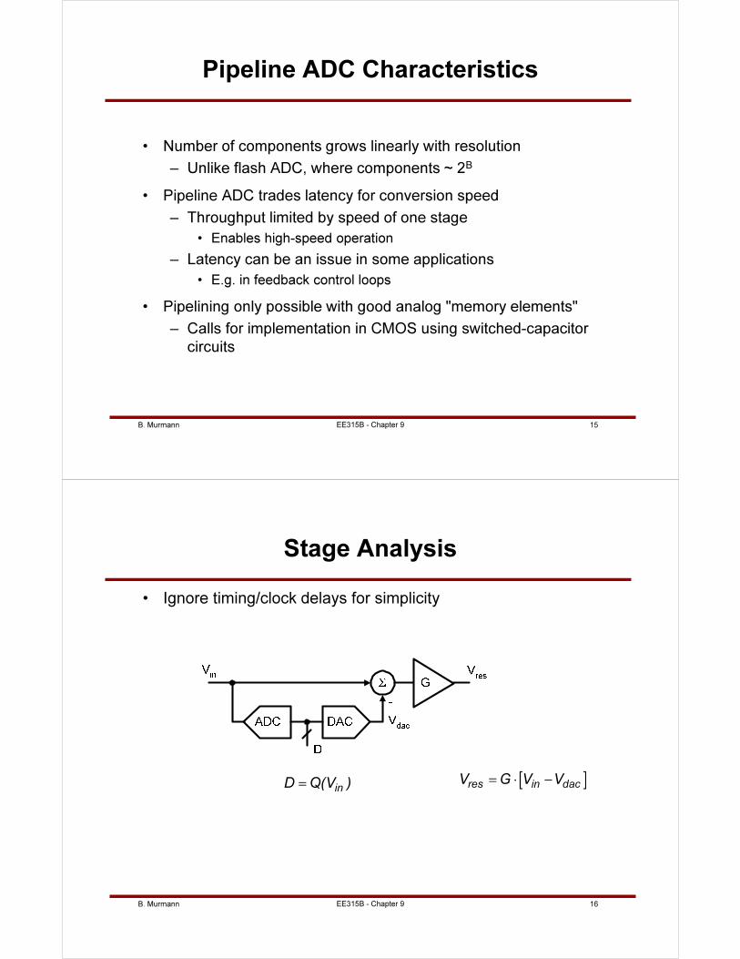
B. Murmann 15
Pipeline ADC Characteristics
• Number of components grows linearly with resolution
– Unlike flash ADC, where components ~ 2B
• Pipeline ADC trades latency for conversion speed
– Throughput limited by speed of one stage
• Enables high-speed operation
– Latency can be an issue in some applications
• E.g. in feedback control loops
• Pipelining only possible with good analog "memory elements"
– Calls for implementation in CMOS using switched-capacitor
circuits
EE315B - Chapter 9
B. Murmann 16
Stage Analysis
• Ignore timing/clock delays for simplicity
[ ]res in dacV G V V= ⋅ −
inD Q(V )=
EE315B - Chapter 9
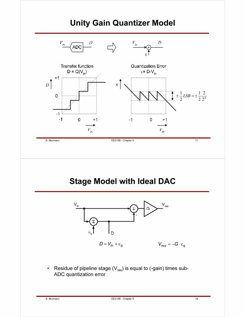
B. Murmann 17
Unity Gain Quantizer Model
BLSB
2
2
2
1
2
1±=±
EE315B - Chapter 9
B. Murmann 18
Stage Model with Ideal DAC
• Residue of pipeline stage (Vres) is equal to (-gain) times sub-
ADC quantization error
in qD V= + εres qV G= − ⋅ ε
EE315B - Chapter 9
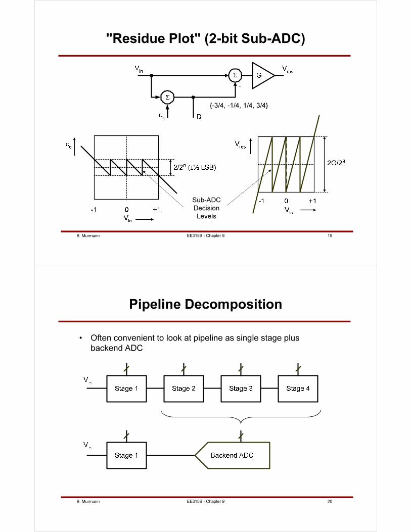
B. Murmann 19
"Residue Plot" (2-bit Sub-ADC)
-3/4, -1/4, 1/4, 3/4
Sub-ADC
Decision
Levels
EE315B - Chapter 9
B. Murmann 20
Pipeline Decomposition
• Often convenient to look at pipeline as single stage plus
backend ADC
EE315B - Chapter 9
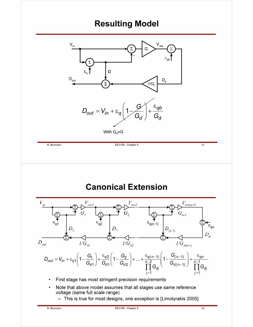
B. Murmann 21
Resulting Model
1qb
out in qd d
GD V
G G
ε = + ε − +
resin
1
bout
q
qb
With Gd=G
EE315B - Chapter 9
B. Murmann 22
Canonical Extension
• First stage has most stringent precision requirements
• Note that above model assumes that all stages use same reference voltage (same full scale range)
– This is true for most designs, one exception is [Limotyrakis 2005]
2 1 11 21 2 1
1 1 2 1
1 1
1 1 1q q(n ) ( n ) qn
out in q n nd d d d(n )
dj dj
j j
GG GD V ...
G G G GG G
− −
− −
−
= =
ε ε ε = + ε − + − + + − + ∏ ∏
EE315B - Chapter 9
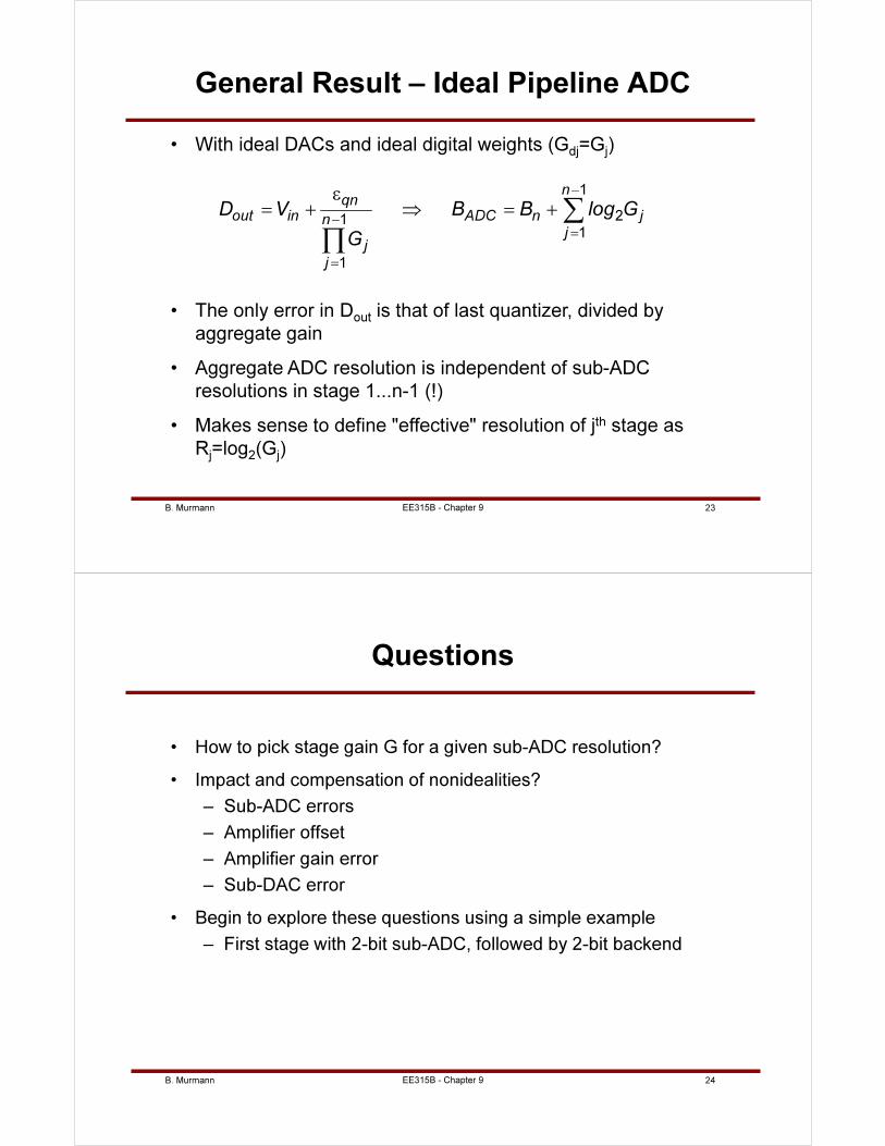
B. Murmann 23
General Result – Ideal Pipeline ADC
• With ideal DACs and ideal digital weights (Gdj=Gj)
1
211
1
nqn
out in ADC n jnj
jj
D V B B log G
G
−
−
=
=
ε
= + ⇒ = +∑∏
• The only error in Dout is that of last quantizer, divided by
aggregate gain
• Aggregate ADC resolution is independent of sub-ADC
resolutions in stage 1...n-1 (!)
• Makes sense to define "effective" resolution of jth stage as
Rj=log2(Gj)
EE315B - Chapter 9
B. Murmann 24
Questions
• How to pick stage gain G for a given sub-ADC resolution?
• Impact and compensation of nonidealities?
– Sub-ADC errors
– Amplifier offset
– Amplifier gain error
– Sub-DAC error
• Begin to explore these questions using a simple example
– First stage with 2-bit sub-ADC, followed by 2-bit backend
EE315B - Chapter 9
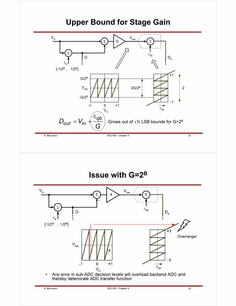
B. Murmann 25
Upper Bound for Stage Gain
0 +1
Vin
-1
Vres
Σ
-
D
Vres
Vin
G1 G
Σ
εq
-1/2B … 1/2B
G/2B
-G/2B
εqb
Σ
εqb
Db
+1
-1
22G/2B
qbout inD V
G
ε
= + Grows out of ±½ LSB bounds for G>2B
EE315B - Chapter 9
B. Murmann 26
Issue with G=2B
in
res
resin
1
q
B B
qb
qb
b
Overrange!
• Any error in sub-ADC decision levels will overload backend ADC and thereby deteriorate ADC transfer function
EE315B - Chapter 9
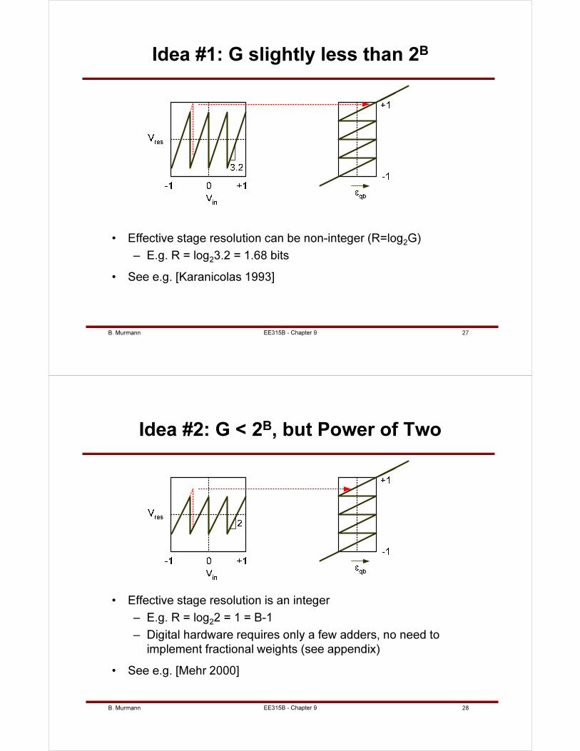
B. Murmann 27
Idea #1: G slightly less than 2B
• Effective stage resolution can be non-integer (R=log2G)
– E.g. R = log23.2 = 1.68 bits
• See e.g. [Karanicolas 1993]
EE315B - Chapter 9
B. Murmann 28
Idea #2: G < 2B, but Power of Two
• Effective stage resolution is an integer
– E.g. R = log22 = 1 = B-1
– Digital hardware requires only a few adders, no need to
implement fractional weights (see appendix)
• See e.g. [Mehr 2000]
EE315B - Chapter 9
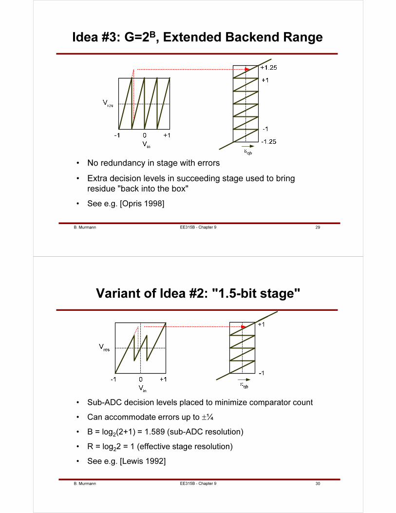
B. Murmann 29
Idea #3: G=2B, Extended Backend Range
• No redundancy in stage with errors
• Extra decision levels in succeeding stage used to bring
residue "back into the box"
• See e.g. [Opris 1998]
EE315B - Chapter 9
B. Murmann 30
Variant of Idea #2: "1.5-bit stage"
• Sub-ADC decision levels placed to minimize comparator count
• Can accommodate errors up to ±¼
• B = log2(2+1) = 1.589 (sub-ADC resolution)
• R = log22 = 1 (effective stage resolution)
• See e.g. [Lewis 1992]
EE315B - Chapter 9
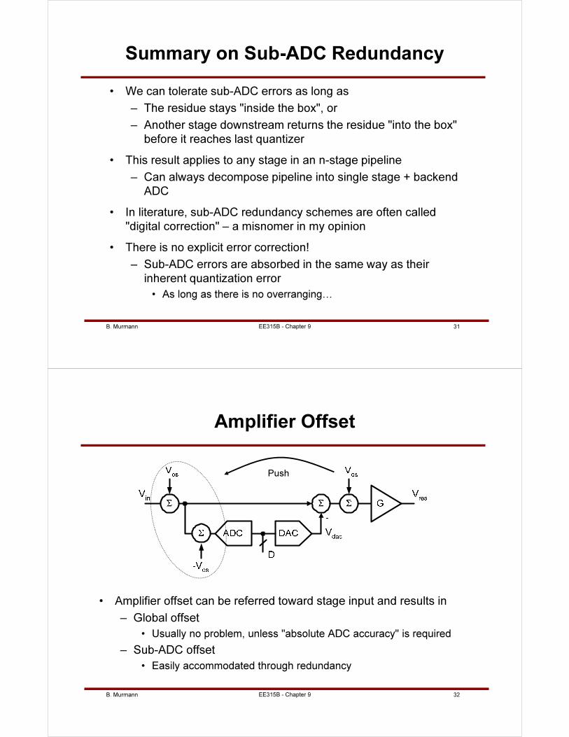
B. Murmann 31
Summary on Sub-ADC Redundancy
• We can tolerate sub-ADC errors as long as
– The residue stays "inside the box", or
– Another stage downstream returns the residue "into the box"
before it reaches last quantizer
• This result applies to any stage in an n-stage pipeline
– Can always decompose pipeline into single stage + backend
ADC
• In literature, sub-ADC redundancy schemes are often called
"digital correction" – a misnomer in my opinion
• There is no explicit error correction!
– Sub-ADC errors are absorbed in the same way as their
inherent quantization error
• As long as there is no overranging…
EE315B - Chapter 9
B. Murmann 32
Amplifier Offset
• Amplifier offset can be referred toward stage input and results in
– Global offset
• Usually no problem, unless "absolute ADC accuracy" is required
– Sub-ADC offset
• Easily accommodated through redundancy
Push
EE315B - Chapter 9
B. Murmann 33
Gain Errors
• Want to make Gd1 = G1+∆
11 1
1
1
1qn
out in q nd
dj
j
GD V ...
GG
−
=
ε + ∆= + ε − + +
∏
EE315B - Chapter 9
B. Murmann 34
Digital Gain Calibration (1)
• Error in analog gain is not a problem as long as "digital gain term" is adjusted appropriately
• Problem
– Need to measure analog gain precisely
• Example
– Digital calibration of a 1-bit first stage with 1-bit redundancy (R=1, B=2)
• Note
– Even if all Gdj are perfectly adjusted to reflect the analog gains, the ADC will have non-zero DNL and INL, bounded by ±0.5LSB. This can be explained by the fact that the residue transitions may not correspond to integer multiples of the backend-LSB. This can cause non-uniformity in the ADC transfer function (DNL, INL) and also non-monotonicity (see [Markus, 2005]).
– In case this cannot be tolerated• Add redundant bits to ADC backend (after combining all bits, final result can be truncated back)
• Calibrate analog gain terms
EE315B - Chapter 9
B. Murmann 35
Digital Gain Calibration (2)
[ ]res in dac
b res qb
V G V V
D V
= ⋅ −
= + ε
EE315B - Chapter 9
B. Murmann 36
Digital Gain Calibration (3)
• Can minimize impact of quantization error using
– Averaging (thermal noise dither)
– Extra backend resolution
Step1: [ ]
[ ]
1 1
2 2
0 25
0 25
( ) ( )inb qb
( ) ( )inb qb
D G V .
D G V .
= ⋅ + + ε
= ⋅ − + εStep2:
1 2 1 20 5
( ) ( ) ( ) ( )b b qb qbD D . G− = ⋅ + ε − ε
EE315B - Chapter 9
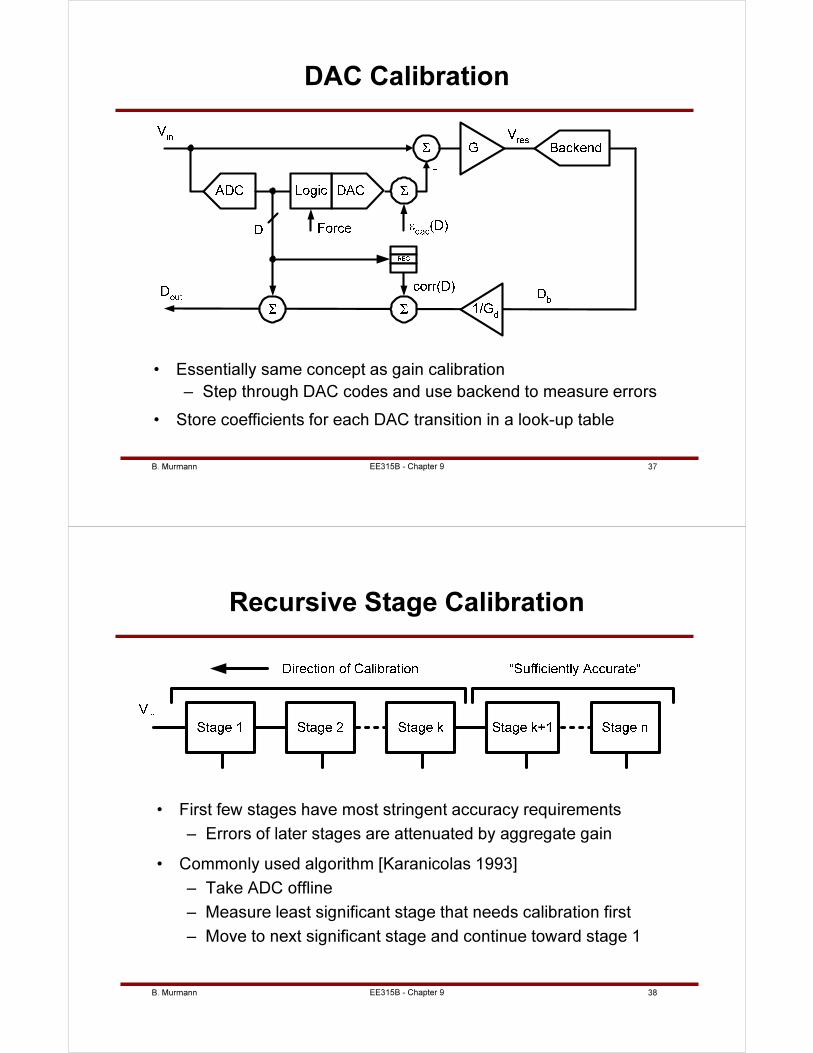
B. Murmann 37
DAC Calibration
• Essentially same concept as gain calibration
– Step through DAC codes and use backend to measure errors
• Store coefficients for each DAC transition in a look-up table
EE315B - Chapter 9
B. Murmann 38
Recursive Stage Calibration
• First few stages have most stringent accuracy requirements
– Errors of later stages are attenuated by aggregate gain
• Commonly used algorithm [Karanicolas 1993]
– Take ADC offline
– Measure least significant stage that needs calibration first
– Move to next significant stage and continue toward stage 1
EE315B - Chapter 9
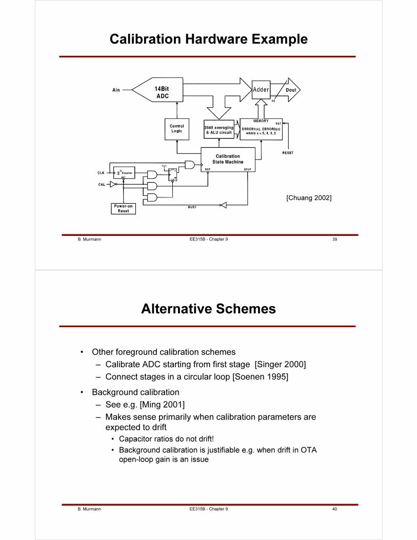
B. Murmann 39
Calibration Hardware Example
[Chuang 2002]
EE315B - Chapter 9
B. Murmann 40
Alternative Schemes
• Other foreground calibration schemes
– Calibrate ADC starting from first stage [Singer 2000]
– Connect stages in a circular loop [Soenen 1995]
• Background calibration
– See e.g. [Ming 2001]
– Makes sense primarily when calibration parameters are
expected to drift
• Capacitor ratios do not drift!
• Background calibration is justifiable e.g. when drift in OTA
open-loop gain is an issue
EE315B - Chapter 9
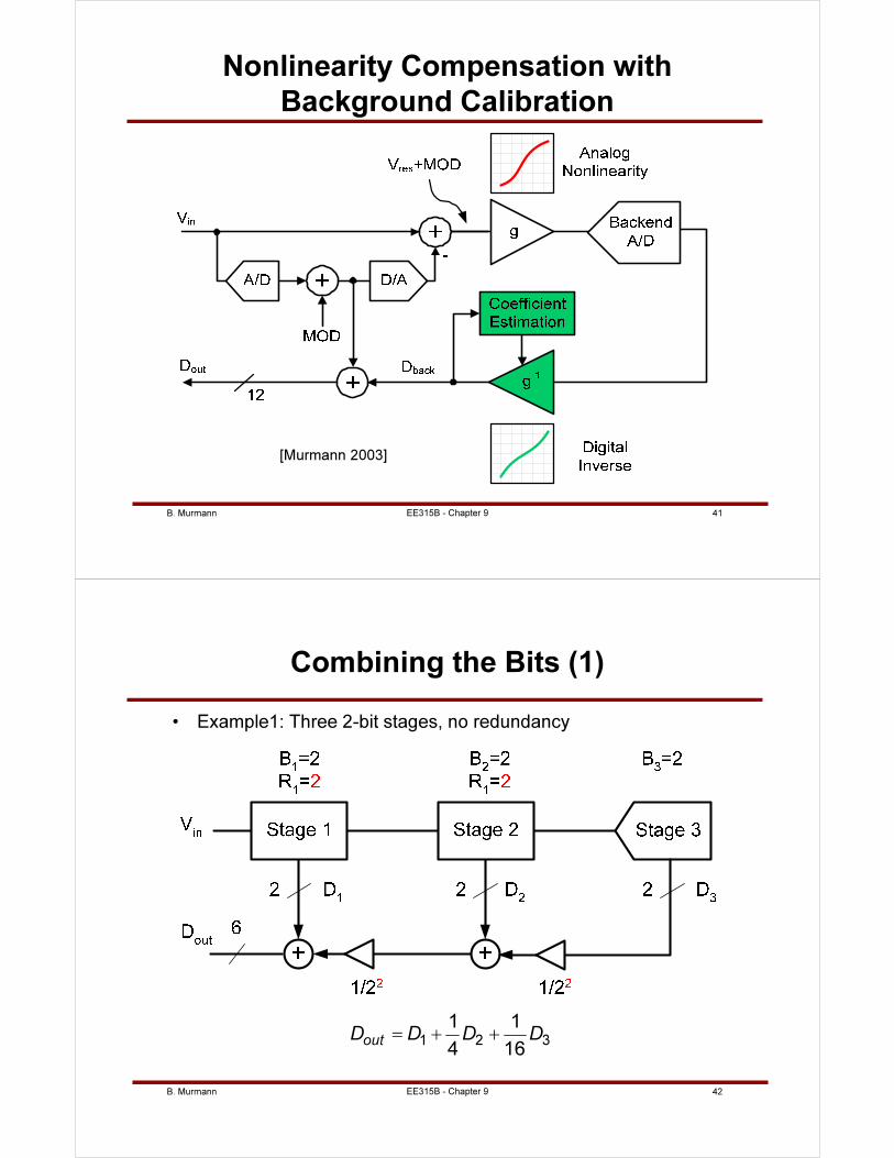
B. Murmann 41
Nonlinearity Compensation with
Background Calibration
[Murmann 2003]
EE315B - Chapter 9
B. Murmann 42
Combining the Bits (1)
• Example1: Three 2-bit stages, no redundancy
1 2 3
1 1
4 16outD D D D= + +
EE315B - Chapter 9
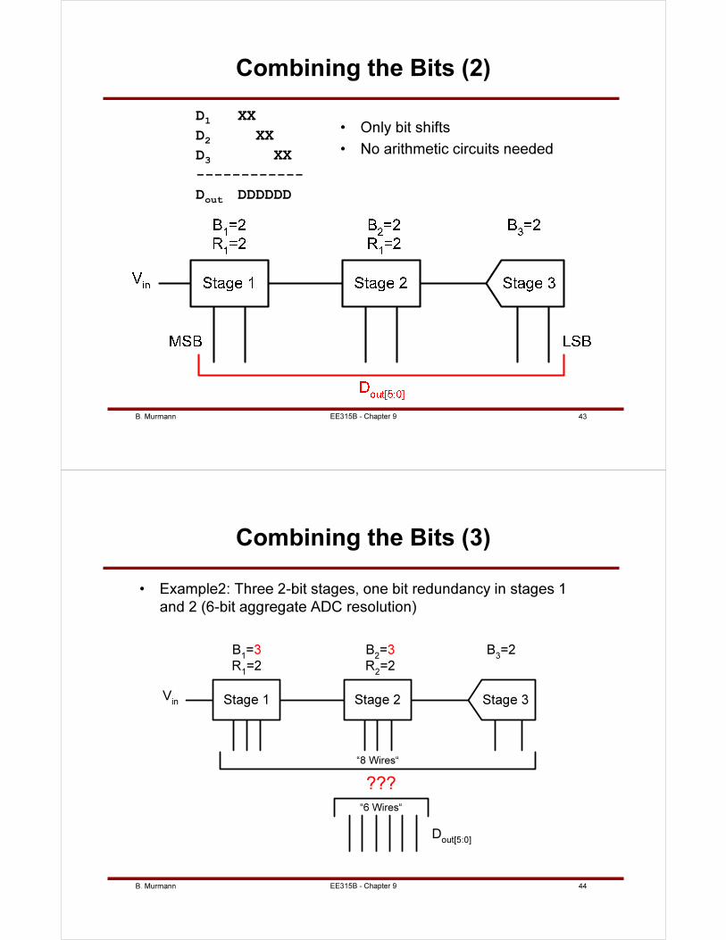
B. Murmann 43
Combining the Bits (2)
• Only bit shifts
• No arithmetic circuits needed
D1
XX
D2
XX
D3
XX
------------
Dout
DDDDDD
EE315B - Chapter 9
B. Murmann 44
Combining the Bits (3)
Stage 2Vin Stage 3Stage 1
Dout[5:0]
B1=3
R1=2
B2=3
R2=2
B3=2
“8 Wires“
“6 Wires“
???
• Example2: Three 2-bit stages, one bit redundancy in stages 1
and 2 (6-bit aggregate ADC resolution)
EE315B - Chapter 9
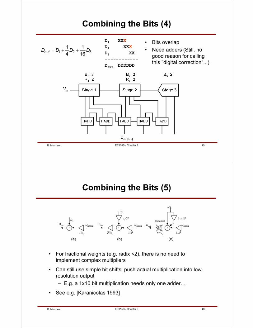
B. Murmann 45
Combining the Bits (4)
• Bits overlap
• Need adders (Still, no
good reason for calling
this "digital correction"...)
D1
XXX
D2
XXX
D3
XX
------------
Dout
DDDDDD
1 2 3
1 1
4 16outD D D D= + +
EE315B - Chapter 9
B. Murmann 46
Combining the Bits (5)
• For fractional weights (e.g. radix <2), there is no need to
implement complex multipliers
• Can still use simple bit shifts; push actual multiplication into low-
resolution output
– E.g. a 1x10 bit multiplication needs only one adder…
• See e.g. [Karanicolas 1993]
EE315B - Chapter 9
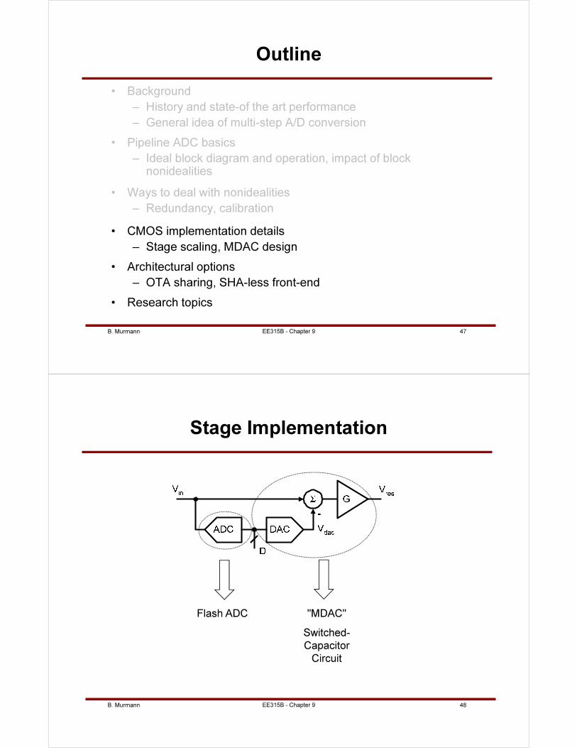
B. Murmann 47
Outline
• Background
– History and state-of the art performance
– General idea of multi-step A/D conversion
• Pipeline ADC basics
– Ideal block diagram and operation, impact of block nonidealities
• Ways to deal with nonidealities
– Redundancy, calibration
• CMOS implementation details
– Stage scaling, MDAC design
• Architectural options
– OTA sharing, SHA-less front-end
• Research topics
EE315B - Chapter 9
B. Murmann 48
Stage Implementation
Flash ADC "MDAC"
Switched-
Capacitor
Circuit
EE315B - Chapter 9
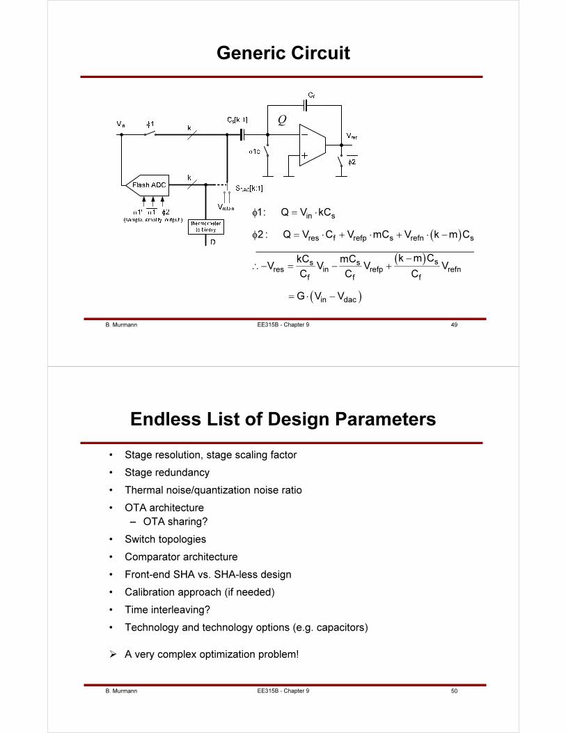
B. Murmann 49
Generic Circuit
( )
( )
( )
in s
res f refp s refn s
ss sres in refp refn
f f f
in dac
1: Q V kC
2 : Q V C V mC V k m C
k m CkC mCV V V V
C C C
G V V
φ = ⋅
φ = ⋅ + ⋅ + ⋅ −
−∴− = − +
= ⋅ −
Q
EE315B - Chapter 9
B. Murmann 50
Endless List of Design Parameters
• Stage resolution, stage scaling factor
• Stage redundancy
• Thermal noise/quantization noise ratio
• OTA architecture
– OTA sharing?
• Switch topologies
• Comparator architecture
• Front-end SHA vs. SHA-less design
• Calibration approach (if needed)
• Time interleaving?
• Technology and technology options (e.g. capacitors)
A very complex optimization problem!
EE315B - Chapter 9
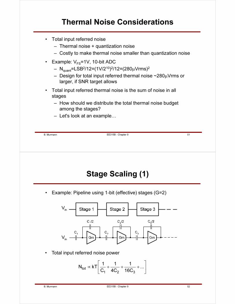
B. Murmann 51
Thermal Noise Considerations
• Total input referred noise
– Thermal noise + quantization noise
– Costly to make thermal noise smaller than quantization noise
• Example: VFS=1V, 10-bit ADC
– Nquant=LSB2/12=(1V/210)2/12=(280µVrms)2
– Design for total input referred thermal noise ~280µVrms or
larger, if SNR target allows
• Total input referred thermal noise is the sum of noise in all
stages
– How should we distribute the total thermal noise budget
among the stages?
– Let's look at an example…
EE315B - Chapter 9
B. Murmann 52
Stage Scaling (1)
• Example: Pipeline using 1-bit (effective) stages (G=2)
• Total input referred noise power
tot
1 2 3
1 1 1N kT ...
C 4C 16C
∝ + + +
EE315B - Chapter 9
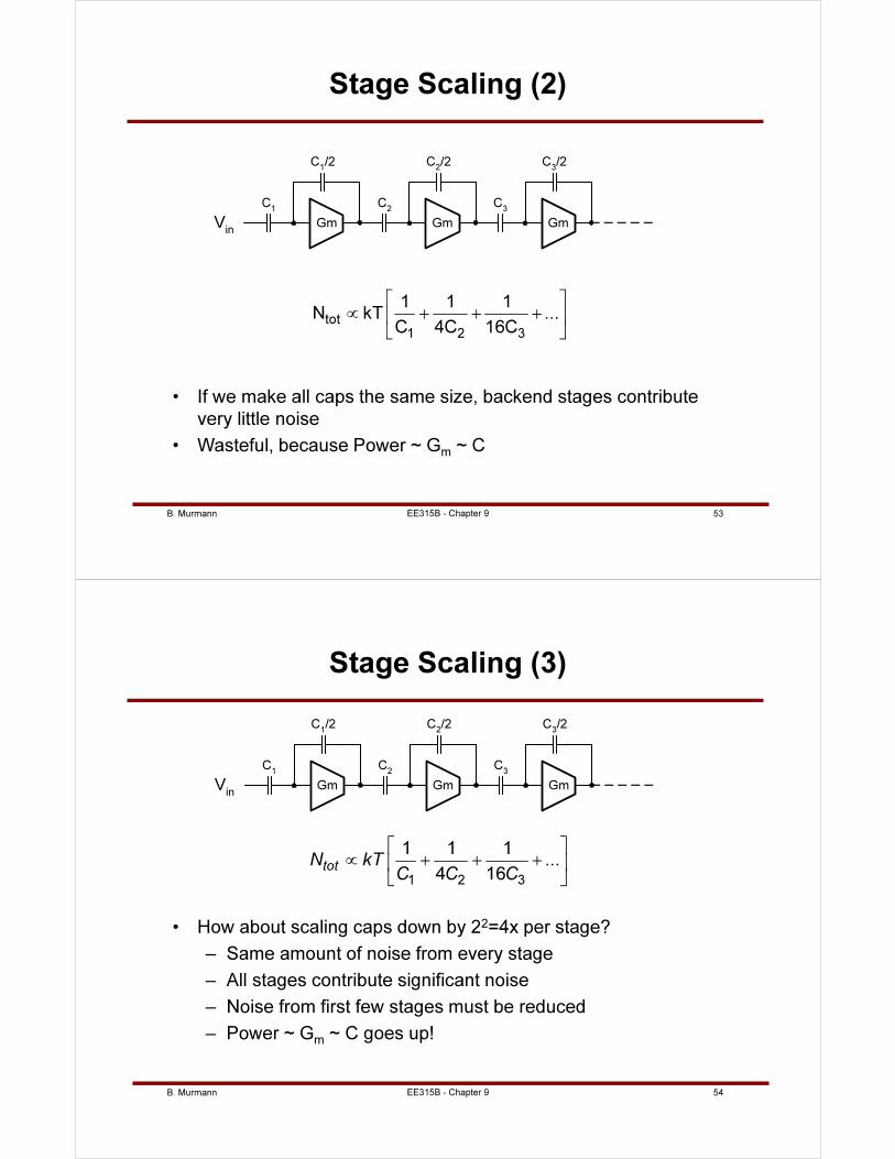
B. Murmann 53
Stage Scaling (2)
C1/2
C1
Gm
C2/2
C2
Gm
C3/2
C3
GmVin
• If we make all caps the same size, backend stages contribute
very little noise
• Wasteful, because Power ~ Gm ~ C
tot
1 2 3
1 1 1N kT ...
C 4C 16C
∝ + + +
EE315B - Chapter 9
B. Murmann 54
Stage Scaling (3)
• How about scaling caps down by 22=4x per stage?
– Same amount of noise from every stage
– All stages contribute significant noise
– Noise from first few stages must be reduced
– Power ~ Gm ~ C goes up!
C1/2
C1
Gm
C2/2
C2
Gm
C3/2
C3
GmVin
1 2 3
1 1 1
4 16totN kT ...
C C C
∝ + + +
EE315B - Chapter 9
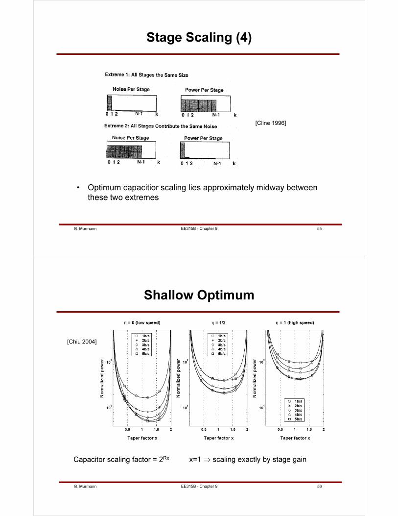
B. Murmann 55
Stage Scaling (4)
• Optimum capacitior scaling lies approximately midway between
these two extremes
[Cline 1996]
EE315B - Chapter 9
B. Murmann 56
Shallow Optimum
[Chiu 2004]
Capacitor scaling factor = 2Rx x=1 ⇒ scaling exactly by stage gain
EE315B - Chapter 9
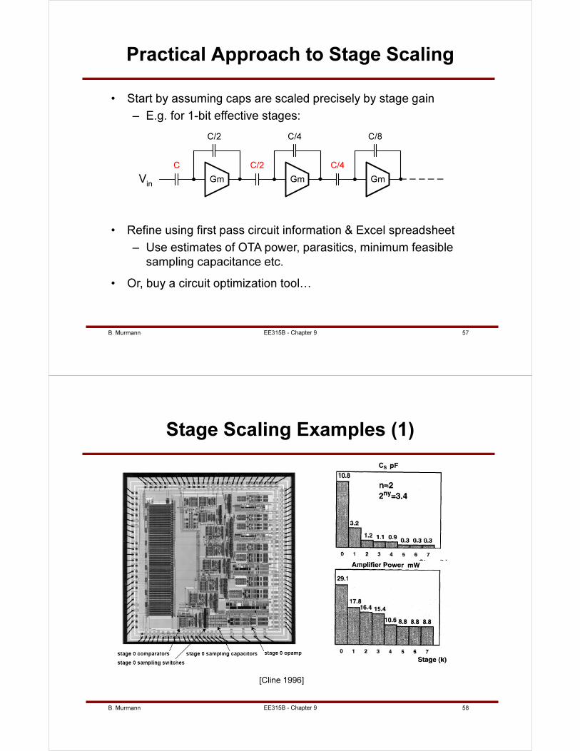
B. Murmann 57
Practical Approach to Stage Scaling
• Start by assuming caps are scaled precisely by stage gain
– E.g. for 1-bit effective stages:
C/2
C
Gm
C/4
C/2
Gm
C/8
C/4
GmVin
• Refine using first pass circuit information & Excel spreadsheet
– Use estimates of OTA power, parasitics, minimum feasible
sampling capacitance etc.
• Or, buy a circuit optimization tool…
EE315B - Chapter 9
B. Murmann 58
Stage Scaling Examples (1)
[Cline 1996]
EE315B - Chapter 9
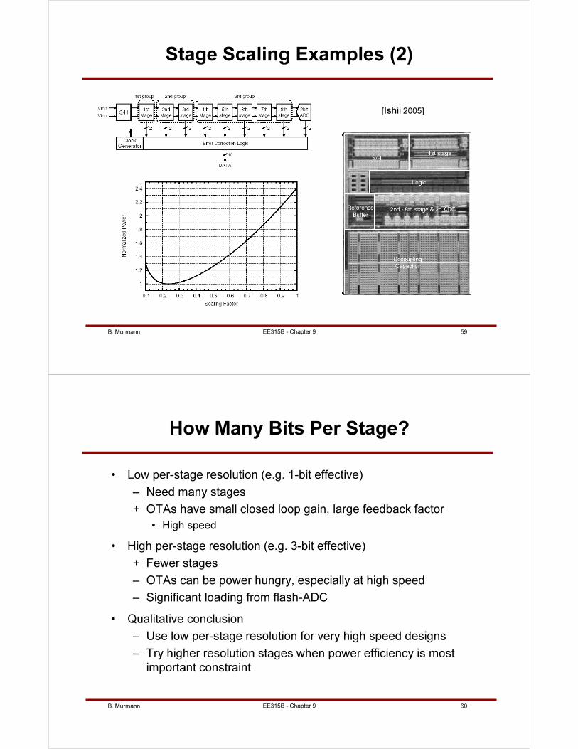
B. Murmann 59
Stage Scaling Examples (2)
[Ishii 2005]
EE315B - Chapter 9
B. Murmann 60
How Many Bits Per Stage?
• Low per-stage resolution (e.g. 1-bit effective)
– Need many stages
+ OTAs have small closed loop gain, large feedback factor
• High speed
• High per-stage resolution (e.g. 3-bit effective)
+ Fewer stages
– OTAs can be power hungry, especially at high speed
– Significant loading from flash-ADC
• Qualitative conclusion
– Use low per-stage resolution for very high speed designs
– Try higher resolution stages when power efficiency is most
important constraint
EE315B - Chapter 9
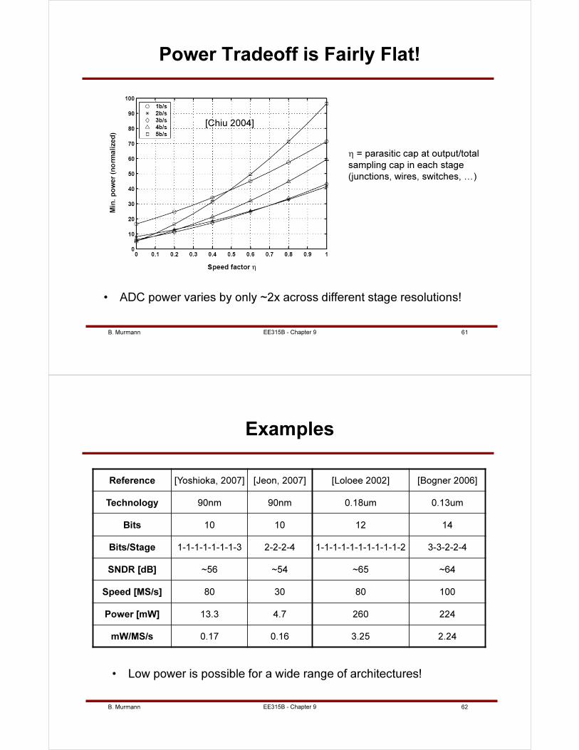
B. Murmann 61
Power Tradeoff is Fairly Flat!
η = parasitic cap at output/total
sampling cap in each stage
(junctions, wires, switches, …)
[Chiu 2004]
• ADC power varies by only ~2x across different stage resolutions!
EE315B - Chapter 9
B. Murmann 62
Examples
• Low power is possible for a wide range of architectures!
Reference [Yoshioka, 2007] [Jeon, 2007] [Loloee 2002] [Bogner 2006]
Technology 90nm 90nm 0.18um 0.13um
Bits 10 10 12 14
Bits/Stage 1-1-1-1-1-1-1-3 2-2-2-4 1-1-1-1-1-1-1-1-1-1-2 3-3-2-2-4
SNDR [dB] ~56 ~54 ~65 ~64
Speed [MS/s] 80 30 80 100
Power [mW] 13.3 4.7 260 224
mW/MS/s 0.17 0.16 3.25 2.24
EE315B - Chapter 9
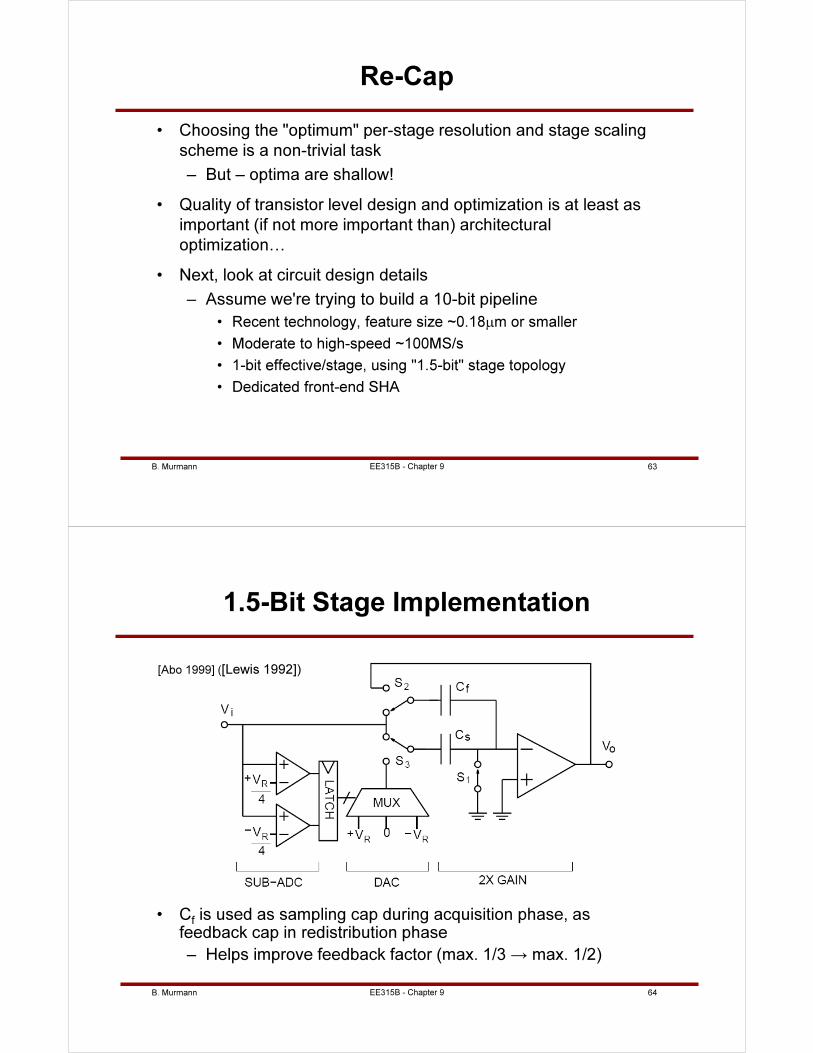
B. Murmann 63
Re-Cap
• Choosing the "optimum" per-stage resolution and stage scaling
scheme is a non-trivial task
– But – optima are shallow!
• Quality of transistor level design and optimization is at least as
important (if not more important than) architectural
optimization…
• Next, look at circuit design details
– Assume we're trying to build a 10-bit pipeline
• Recent technology, feature size ~0.18µm or smaller
• Moderate to high-speed ~100MS/s
• 1-bit effective/stage, using "1.5-bit" stage topology
• Dedicated front-end SHA
EE315B - Chapter 9
B. Murmann 64
1.5-Bit Stage Implementation
• Cf is used as sampling cap during acquisition phase, as feedback cap in redistribution phase
– Helps improve feedback factor (max. 1/3 → max. 1/2)
[Abo 1999] ([Lewis 1992])
EE315B - Chapter 9
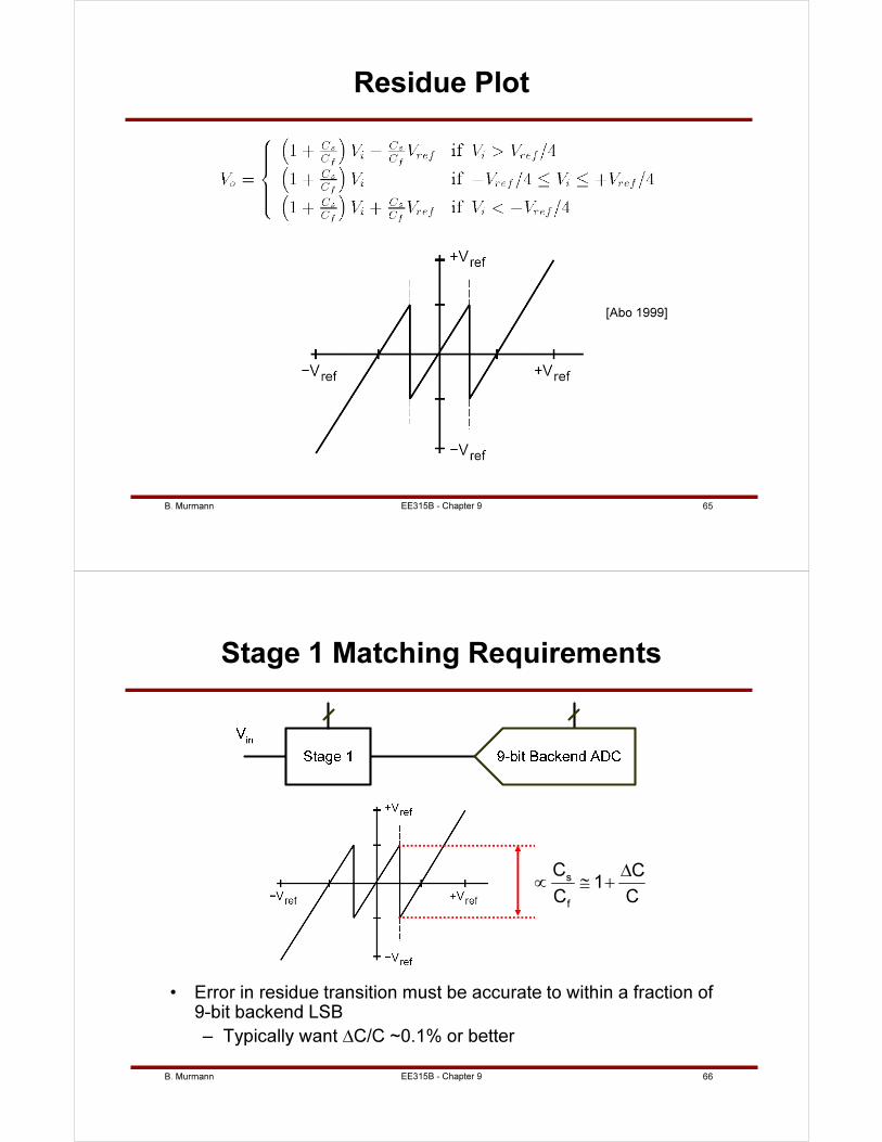
B. Murmann 65
Residue Plot
[Abo 1999]
EE315B - Chapter 9
B. Murmann 66
Stage 1 Matching Requirements
s
f
C C1
C C
∆∝ ≅ +
• Error in residue transition must be accurate to within a fraction of 9-bit backend LSB
– Typically want ∆C/C ~0.1% or better
EE315B - Chapter 9
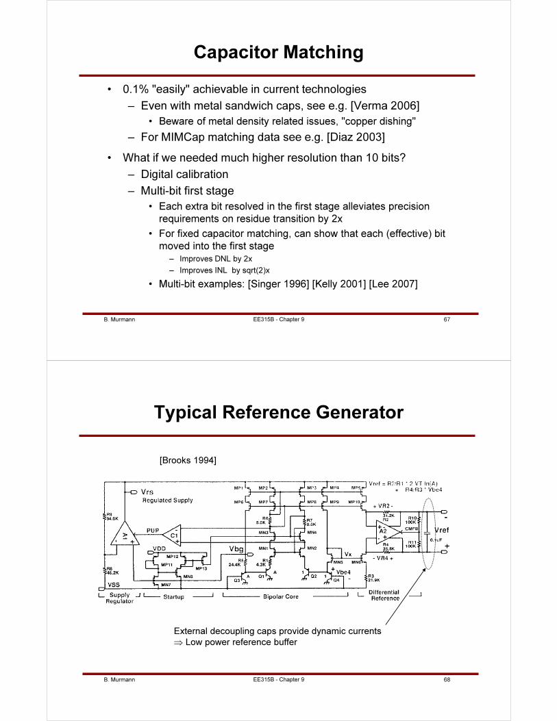
B. Murmann 67
Capacitor Matching
• 0.1% "easily" achievable in current technologies
– Even with metal sandwich caps, see e.g. [Verma 2006]
• Beware of metal density related issues, "copper dishing"
– For MIMCap matching data see e.g. [Diaz 2003]
• What if we needed much higher resolution than 10 bits?
– Digital calibration
– Multi-bit first stage
• Each extra bit resolved in the first stage alleviates precision
requirements on residue transition by 2x
• For fixed capacitor matching, can show that each (effective) bit
moved into the first stage– Improves DNL by 2x
– Improves INL by sqrt(2)x
• Multi-bit examples: [Singer 1996] [Kelly 2001] [Lee 2007]
EE315B - Chapter 9
B. Murmann 68
Typical Reference Generator
[Brooks 1994]
External decoupling caps provide dynamic currents
⇒ Low power reference buffer
EE315B - Chapter 9
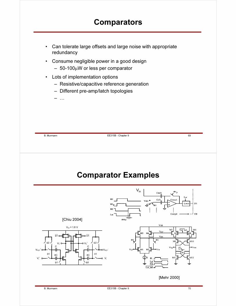
B. Murmann 69
Comparators
• Can tolerate large offsets and large noise with appropriate
redundancy
• Consume negligible power in a good design
– 50-100µW or less per comparator
• Lots of implementation options
– Resistive/capacitive reference generation
– Different pre-amp/latch topologies
– …
EE315B - Chapter 9
B. Murmann 70
Comparator Examples
[Chiu 2004]
[Mehr 2000]
Vin
EE315B - Chapter 9
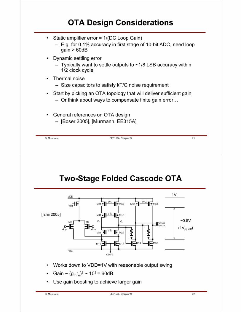
B. Murmann 71
OTA Design Considerations
• Static amplifier error = 1/(DC Loop Gain)
– E.g. for 0.1% accuracy in first stage of 10-bit ADC, need loop gain > 60dB
• Dynamic settling error
– Typically want to settle outputs to ~1/8 LSB accuracy within 1/2 clock cycle
• Thermal noise
– Size capacitors to satisfy kT/C noise requirement
• Start by picking an OTA topology that will deliver sufficient gain
– Or think about ways to compensate finite gain error…
• General references on OTA design
– [Boser 2005], [Murmann, EE315A]
EE315B - Chapter 9
B. Murmann 72
Two-Stage Folded Cascode OTA
• Works down to VDD=1V with reasonable output swing
• Gain ~ (gmro)3 ~ 103 = 60dB
• Use gain boosting to achieve larger gain
[Ishii 2005]
1V
~0.5V
(1Vpp,diff)
EE315B - Chapter 9

B. Murmann 73
How Fast Can We Go? (1)
• Non-dominant pole in two-stage amplifier hard to move past fT/5
• For 73 degrees phase margin (optimum for fast settling), loop
crossover frequency is 1/3 of non-dominant pole frequency
• Settling linearly to 0.1% precision takes 7 loop time constants;
typically budget ~10 time constants
• Ideally, we'd have 1/2 clock cycle to settle linearly, but there is
some time needed for slewing and non-overlap clock timing
– Assume 60% of half cycle is available for linear settling
• In summary
1 12 0 5 0 6
5 3 10 80
T TCLK,max
f ff . .= ⋅ π ⋅ ⋅ =
EE315B - Chapter 9
B. Murmann 74
How Fast Can We Go? (2)
• Sampling speeds of 200-300MHz are "easily" achievable in today's technologies
– fT is no longer a showstopper
– Speed ultimately constrained by power, power efficiency and/or clock jitter
TechnologyNMOS fT
(at moderate VGS-Vt ~150mV)fCLK,max = fT/80
0.35um 10GHz 125 MHz
0.18um 30GHz 375 MHz
90nm 90GHz 1.125GHz (?)
EE315B - Chapter 9
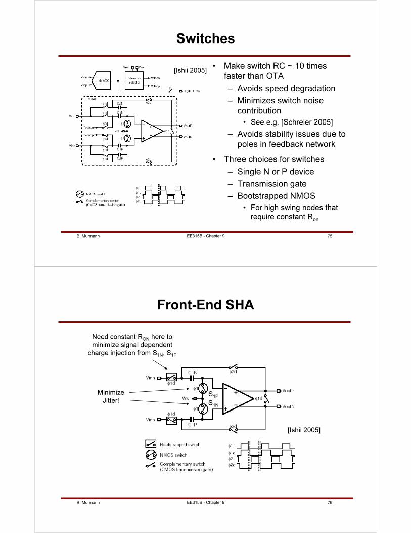
B. Murmann 75
Switches
• Make switch RC ~ 10 times
faster than OTA
– Avoids speed degradation
– Minimizes switch noise
contribution
• See e.g. [Schreier 2005]
– Avoids stability issues due to
poles in feedback network
• Three choices for switches
– Single N or P device
– Transmission gate
– Bootstrapped NMOS
• For high swing nodes that
require constant Ron
[Ishii 2005]
EE315B - Chapter 9
B. Murmann 76
Front-End SHA
[Ishii 2005]
Minimize
Jitter!
Need constant RON here to
minimize signal dependent
charge injection from S1N, S1P
S1P
S1N
EE315B - Chapter 9
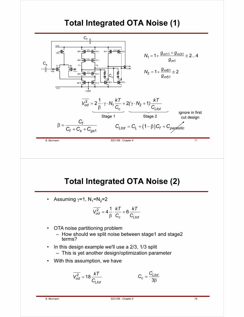
B. Murmann 77
Total Integrated OTA Noise (1)
2
1 2
12 2 1od
c Ltot
kT kTV N ( N )
C C= ⋅ γ ⋅ + γ ⋅ +
β
1
f
f s gs
C
C C Cβ =
+ +
11 311
1
612
51
1 2 4
1 2
m m
m
m
m
g gN ...
g
gN
g
+
= + ≅
= + ≅
( )1Ltot L f parasiticC C C C= + −β +
Stage 1 Stage 2
Cs
Cf
Cc
ignore in first
cut design
EE315B - Chapter 9
B. Murmann 78
Total Integrated OTA Noise (2)
• Assuming γ=1, N1=N2=2
2 14 6od
c Ltot
kT kTV
C C= ⋅ +
β
• OTA noise partitioning problem
– How should we split noise between stage1 and stage2 terms?
• In this design example we'll use a 2/3, 1/3 split
– This is yet another design/optimization parameter
• With this assumption, we have
218od
Ltot
kTV
C=
3
Ltotc
CC =
β
EE315B - Chapter 9
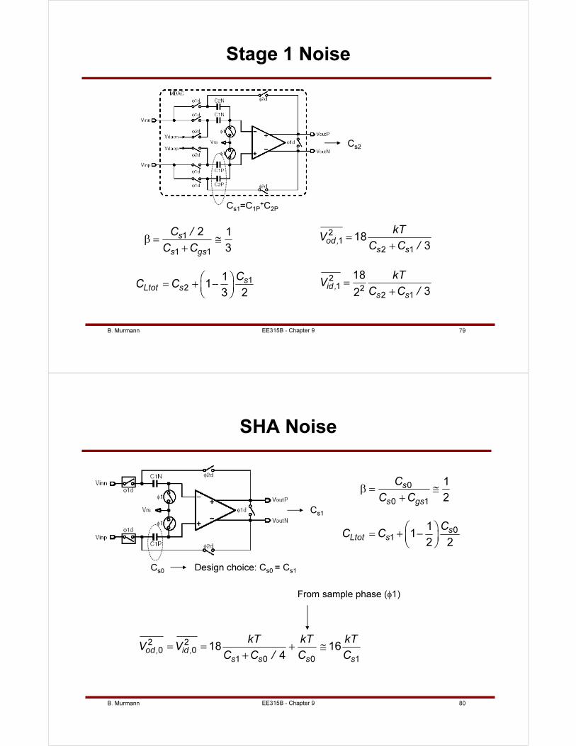
B. Murmann 79
Stage 1 Noise
1
1 1
2 1
3
s
s gs
C /
C Cβ = ≅
+
Cs1=C1P+C2P
Cs2
12
11
3 2
sLtot s
CC C
= + −
2
1
2 1
183
od,s s
kTV
C C /=
+
2
1 22 1
18
32id ,
s s
kTV
C C /=
+
EE315B - Chapter 9
B. Murmann 80
SHA Noise
0
0 1
1
2
s
s gs
C
C Cβ = ≅
+
Cs0
Cs1
01
11
2 2
sLtot s
CC C
= + −
2 2
0 0
1 0 0 1
18 164
od, id ,s s s s
kT kT kTV V
C C / C C= = + ≅
+
From sample phase (φ1)
Design choice: Cs0 = Cs1
EE315B - Chapter 9
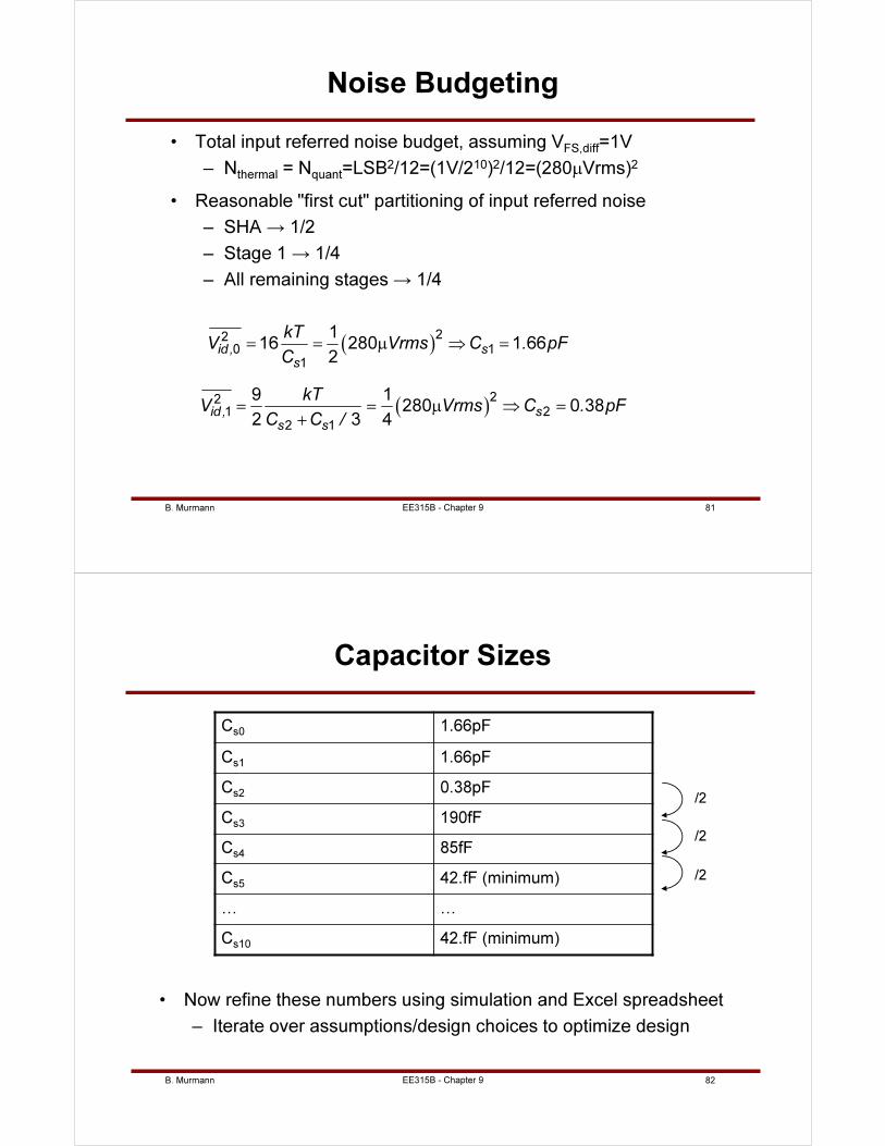
B. Murmann 81
Noise Budgeting
• Total input referred noise budget, assuming VFS,diff=1V
– Nthermal = Nquant=LSB2/12=(1V/210)2/12=(280µVrms)2
• Reasonable "first cut" partitioning of input referred noise
– SHA → 1/2
– Stage 1 → 1/4
– All remaining stages → 1/4
( )22
1 2
2 1
9 1280 0 38
2 3 4id , s
s s
kTV Vrms C . pF
C C /= = µ ⇒ =
+
( )22
0 1
1
116 280 1 66
2id , s
s
kTV Vrms C . pF
C= = µ ⇒ =
EE315B - Chapter 9
B. Murmann 82
Capacitor Sizes
• Now refine these numbers using simulation and Excel spreadsheet
– Iterate over assumptions/design choices to optimize design
Cs0
1.66pF
Cs1
1.66pF
Cs2
0.38pF
Cs3
190fF
Cs4
85fF
Cs5
42.fF (minimum)
… …
Cs10
42.fF (minimum)
/2
/2
/2
EE315B - Chapter 9
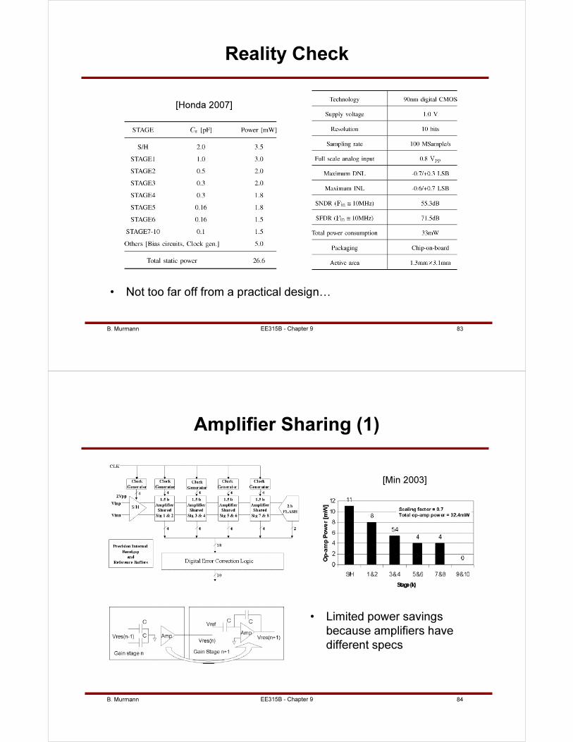
B. Murmann 83
Reality Check
[Honda 2007]
• Not too far off from a practical design…
EE315B - Chapter 9
B. Murmann 84
Amplifier Sharing (1)
• Limited power savings
because amplifiers have
different specs
[Min 2003]
EE315B - Chapter 9
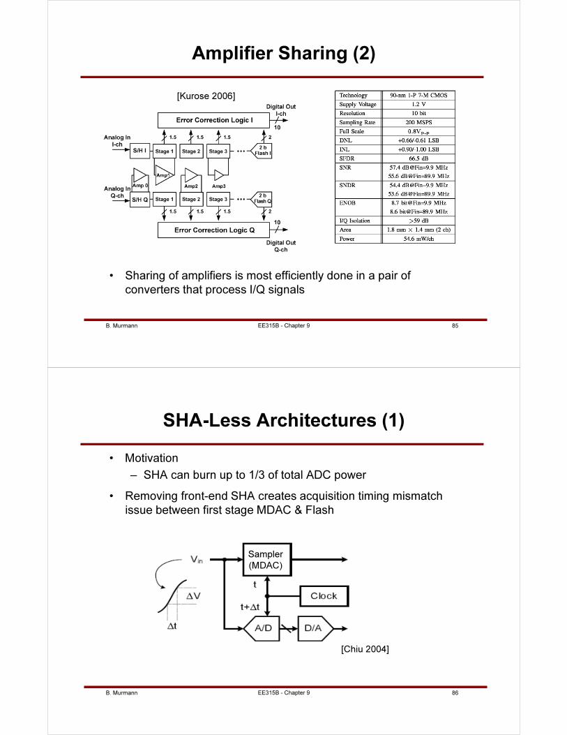
B. Murmann 85
Amplifier Sharing (2)
• Sharing of amplifiers is most efficiently done in a pair of
converters that process I/Q signals
[Kurose 2006]
EE315B - Chapter 9
B. Murmann 86
SHA-Less Architectures (1)
• Motivation
– SHA can burn up to 1/3 of total ADC power
• Removing front-end SHA creates acquisition timing mismatch
issue between first stage MDAC & Flash
Sampler
(MDAC)
[Chiu 2004]
EE315B - Chapter 9
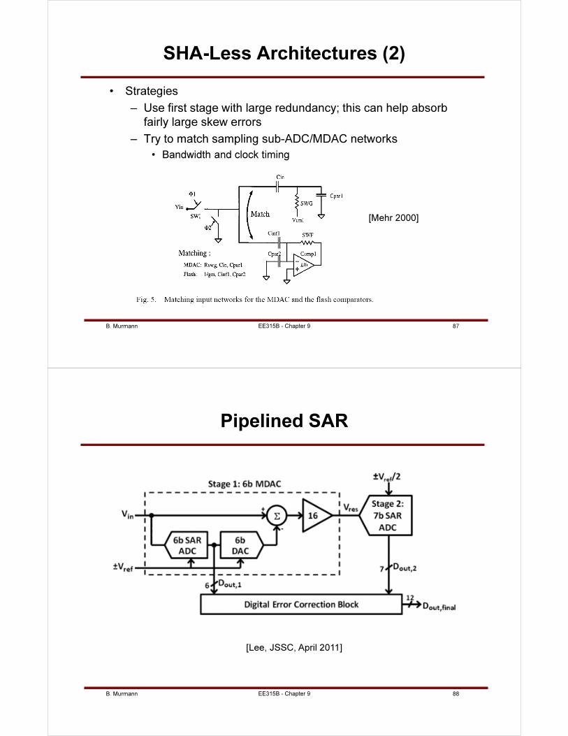
B. Murmann 87
SHA-Less Architectures (2)
• Strategies
– Use first stage with large redundancy; this can help absorb
fairly large skew errors
– Try to match sampling sub-ADC/MDAC networks
• Bandwidth and clock timing
[Mehr 2000]
EE315B - Chapter 9
B. Murmann 88
Pipelined SAR
EE315B - Chapter 9
[Lee, JSSC, April 2011]
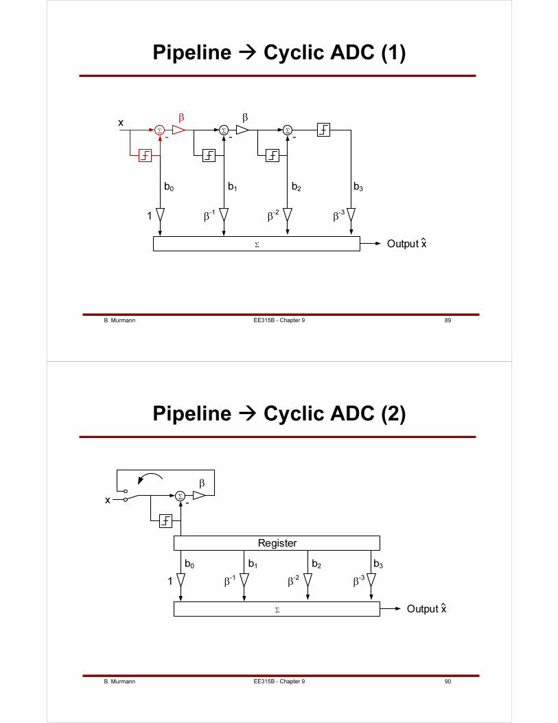
B. Murmann 89
Pipeline Cyclic ADC (1)
Σ Σ
b3
Σ
x
b0 b1 b2
- - -
Output x
β-1
β-2
β-3
1
Σ
ββ
EE315B - Chapter 9
B. Murmann 90
Pipeline Cyclic ADC (2)
b3
Σx
b0 b1 b2
-
Output x
β-1
β-2
β-31
Σ
β
Register
EE315B - Chapter 9
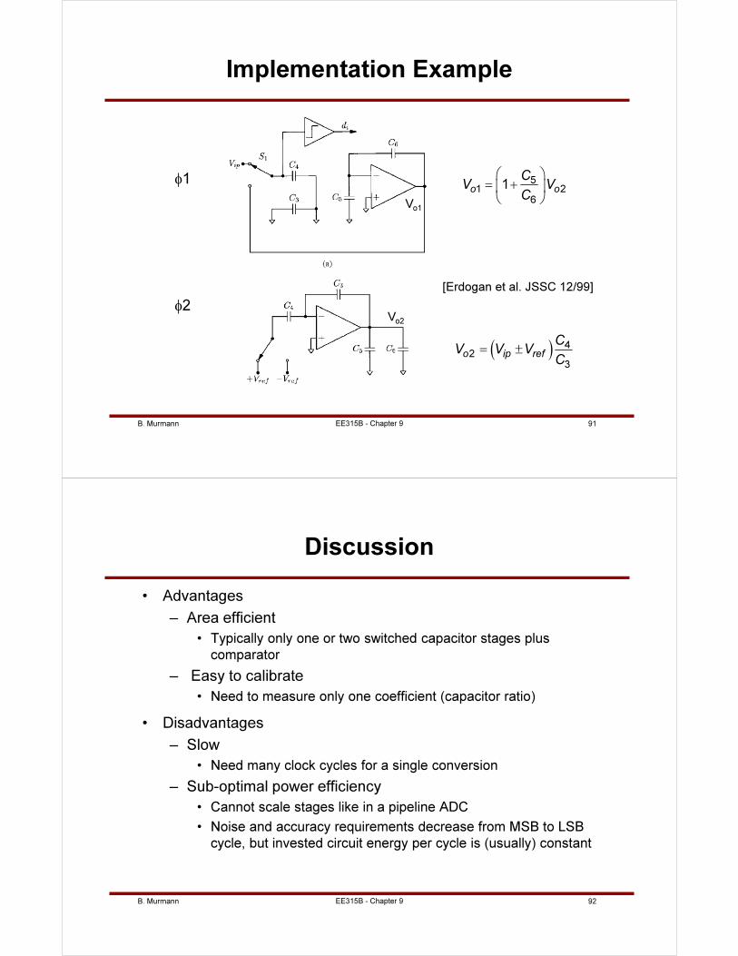
B. Murmann 91
Implementation Example
[Erdogan et al. JSSC 12/99]
φ1
φ2
( ) 42
3
o ip ref
CV V V
C= ±
51 2
6
1o o
CV V
C
= +
Vo2
Vo1
EE315B - Chapter 9
B. Murmann 92
Discussion
• Advantages
– Area efficient
• Typically only one or two switched capacitor stages plus
comparator
– Easy to calibrate
• Need to measure only one coefficient (capacitor ratio)
• Disadvantages
– Slow
• Need many clock cycles for a single conversion
– Sub-optimal power efficiency
• Cannot scale stages like in a pipeline ADC
• Noise and accuracy requirements decrease from MSB to LSB
cycle, but invested circuit energy per cycle is (usually) constant
EE315B - Chapter 9
B. Murmann 93
Selected References (1)
• General– S. Kawahito, "Low-Power Design of Pipeline A/D Converters," Proc. CICC, pp.
505-512, Sep. 2006.
• Redundancy & Calibration– S. H. Lewis et al., "A 10-b 20-Msample/s analog-to-digital converter," IEEE
JSSC, pp. 351-358, Mar. 1992.
– A. N. Karanicolas et al. "A 15-b 1-Msample/s digitally self-calibrated pipeline ADC," IEEE J. Of Solid-State Circuits, pp. 1207-1215, Dec. 1993.
– E. G. Soenen et al., "An architecture and an algorithm for fully digital correction of monolithic pipelined ADCs," IEEE TCAS II, pp. 143-153, Mar. 1995.
– I. E. Opris et al., "A single-ended 12-bit 20 MSample/s self-calibrating pipeline A/D converter," IEEE JSSC, pp. 1898-1903, Dec. 1998.
– L. Singer et al., "A 12 b 65 MSample/s CMOS ADC with 82 dB SFDR at 120 MHz," ISSCC Dig. Techn. Papers, pp. 38-39, Feb. 2000.
– I. Mehr et al., "A 55-mW, 10-bit, 40-Msample/s Nyquist-rate CMOS ADC," IEEE JSSC, pp. 318-325, Mar. 2000.
– J. Ming et al., "An 8-bit 80-Msample/s pipelined analog-to-digital converter with background calibration," IEEE JSSC, pp. 1489-1497, Oct. 2001.
– S.-Y. Chuang et al., "A Digitally Self-Calibrating 14-bit 10-MHz CMOS Pipelined A/D Converter," IEEE JSSC, pp. 674-683, Jun. 2002.
– J. Markus et al., "On the monotonicity and linearity of ideal radix-based A/D converters," IEEE Trans. Instr. and Measurement, pp. 2454-2457, Dec. 2005.
EE315B - Chapter 9
B. Murmann 94
Selected References (2)
• Implementation– T. Cho, "Low-Power Low-Voltage Analog-to-Digital Conversion Techniques
using Pipelined Architecures, PhD Dissertation, UC Berkeley, 1995, http://kabuki.eecs.berkeley.edu/~tcho/Thesis1.pdf.
– L. A. Singer at al., "A 14-bit 10-MHz calibration-free CMOS pipelined A/D converter," VLSI Circuit Symposium, pp. 94-95, Jun. 1996.
– A. Abo, "Design for Reliability of Low-voltage, Switched-capacitor Circuits," PhD Dissertation, UC Berkeley, 1999, http://kabuki.eecs.berkeley.edu/~abo/abothesis.pdf.
– D. Kelly et al., "A 3V 340mW 14b 75MSPS CMOS ADC with 85dB SFDR at Nyquist," ISSCC Dig. Techn. Papers, pp. 134-135, Feb. 2001.
– A. Loloee, et. al, “A 12b 80-MSs Pipelined ADC Core with 190 mW Consumption from 3 V in 0.18-um, Digital CMOS”, Proc. ESSCIRC, pp. 467-469, 2002
– B.-M. Min et al., "A 69-mW 10-bit 80-MSample/s Pipelined CMOS ADC," IEEE JSSC, pp. 2031-2039, Dec. 2003.
– Y. Chiu, et al., "A 14-b 12-MS/s CMOS pipeline ADC with over 100-dB SFDR,” IEEE JSSC, pp. 2139-2151, Dec. 2004.
– S. Limotyrakis et al., "A 150-MS/s 8-b 71-mW CMOS time-interleaved ADC," IEEE JSSC, pp. 1057-1067, May 2005.
– T. N. Andersen et al., "A Cost-Efficient High-Speed 12-bit Pipeline ADC in 0.18-um Digital CMOS," IEEE JSSC, pp. 1506-1513, Jul 2005.
EE315B - Chapter 9
B. Murmann 95
Selected References (3)
– P. Bogner et al., "A 14b 100MS/s digitally self-calibrated pipelined ADC in 0.13um CMOS," ISSCC Dig. Techn. Papers, pp. 832-833, Feb. 2006.
– D. Kurose et al., "55-mW 200-MSPS 10-bit Pipeline ADCs for Wireless Receivers," IEEE JSSC, pp. 1589-1595, Jul. 2006.
– S. Bardsley et al., "A 100-dB SFDR 80-MSPS 14-Bit 0.35um BiCMOS Pipeline ADC," IEEE JSSC, pp. 2144-2153, Sep. 2006.
– A. M. A. Ali et al, "A 14-bit 125 MS/s IF/RF Sampling Pipelined ADC With 100 dB SFDR and 50 fs Jitter," IEEE JSSC, pp. 1846-1855, Aug. 2006.
– S. K. Gupta, "A 1-GS/s 11-bit ADC With 55-dB SNDR, 250-mW Power Realized by a High Bandwidth Scalable Time-Interleaved Architecture," IEEE JSSC, 2650-2657, Dec. 2006.
– M. Yoshioka et al., "A 0.8V 10b 80MS/s 6.5mW Pipelined ADC with Regulated Overdrive Voltage Biasing," ISSCC Dig. Techn. Papers, pp. 452-453, Feb. 2007.
– Y.-D. Jeon et al., "A 4.7mW 0.32mm2 10b 30MS/s Pipelined ADC Without a Front-End S/H in 90nm CMOS," ISSCC Dig. Techn. Papers, pp. 456-457, Feb. 2007.
– K.-H. Lee et al., "Calibration-free 14b 70MS/s 0.13um CMOS pipeline A/D converters based on highmatching 3D symmetric capacitors," Electronics Letters, pp. 35-36, Mar. 15, 2007.
– K. Honda et al., "A Low-Power Low-Voltage 10-bit 100-MSample/s Pipeline A/D Converter Using Capacitance Coupling Techniques," IEEE JSSC, pp. 757-765, Apr. 2007.
EE315B - Chapter 9
B. Murmann 96
Selected References (4)
• Per-Stage Resolution and Stage Scaling
– D. W. Cline, "Noise, Speed, and Power Tradeoffs in Pipelined Analog to Digital Converters", PhD Dissertation, UC Berkeley, November, 1995, http://kabuki.eecs.berkeley.edu/~cline/thesis/thesis.pdf.
– D. W. Cline et al., "A power optimized 13-b 5 MSamples/s pipelined analog-to-digital converter in 1.2um CMOS," IEEE JSSC, Mar. 1996
– Y. Chiu, "High-Performance Pipeline A/D Converter Design in Deep-Submicron CMOS," PhD Dissertation, UC Berkeley, 2004.
– H. Ishii et al., "A 1.0 V 40mW 10b 100MS/s pipeline ADC in 90nm CMOS," Proc. CICC, pp. 395-398, Sep. 2005.
• OTA Design, Noise
– B. E. Boser, "Analog Circuit Design with Submicron Transistors," Presentation at IEEE Santa Clara Valley, May 19, 2005, http://www.ewh.ieee.org/r6/scv/ssc/May1905.htm
– R. Schreier et al., "Design-oriented estimation of thermal noise in switched-capacitor circuits," IEEE TCAS I, pp. 2358-2368, Nov. 2005.
– B. Murmann, "Thermal Noise in Track-and-Hold Circuits: Analysis and Simulation Techniques," IEEE Solid-State Circuits Magazine, vol.4, no.2, pp. 46-54, June 2012.
EE315B - Chapter 9
B. Murmann 97
Selected References (5)
• Capacitor Matching Data
– C. H. Diaz et al., "CMOS technology for MS/RF SoC," IEEE Trans. Electron Devices, pp. 557-566, Mar. 2003.
– A. Verma et al., "Frequency-Based Measurement of Mismatches Between Small Capacitors," Proc. CICC, pp. 481-484, Sep. 2006.
– V. Tripathi and B. Murmann, "Mismatch Characterization of Small Metal Fringe Capacitors," CICC 2013.
• Reference Generator
– T. L. Brooks et al., "A low-power differential CMOS bandgap reference," ISSCC Dig. Techn. Papers, pp. 248-249, Feb. 1994.
EE315B - Chapter 9
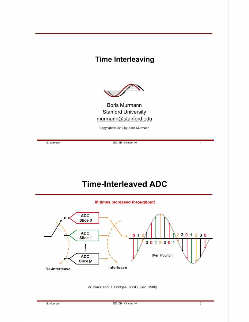
B. Murmann 1EE315B - Chapter 10
Time Interleaving
Boris Murmann
Stanford University
Copyright © 2013 by Boris Murmann
B. Murmann 2
Time-Interleaved ADC
[W. Black and D. Hodges, JSSC, Dec. 1980]
[Ken Poulton]
M
M times increased throughput!
EE315B - Chapter 10
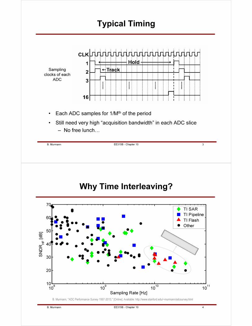
B. Murmann 3EE315B - Chapter 10
Typical Timing
• Each ADC samples for 1/Mth of the period
• Still need very high “acquisition bandwidth” in each ADC slice
– No free lunch…
Sampling
clocks of each
ADC
B. Murmann 4
Why Time Interleaving?
108
109
1010
1011
10
20
30
40
50
60
70
Sampling Rate [Hz]
SN
DRHF [dB
]
TI SAR
TI Pipeline
TI Flash
Other
B. Murmann, "ADC Performance Survey 1997-2013," [Online]. Available: http://www.stanford.edu/~murmann/adcsurvey.html
EE315B - Chapter 10
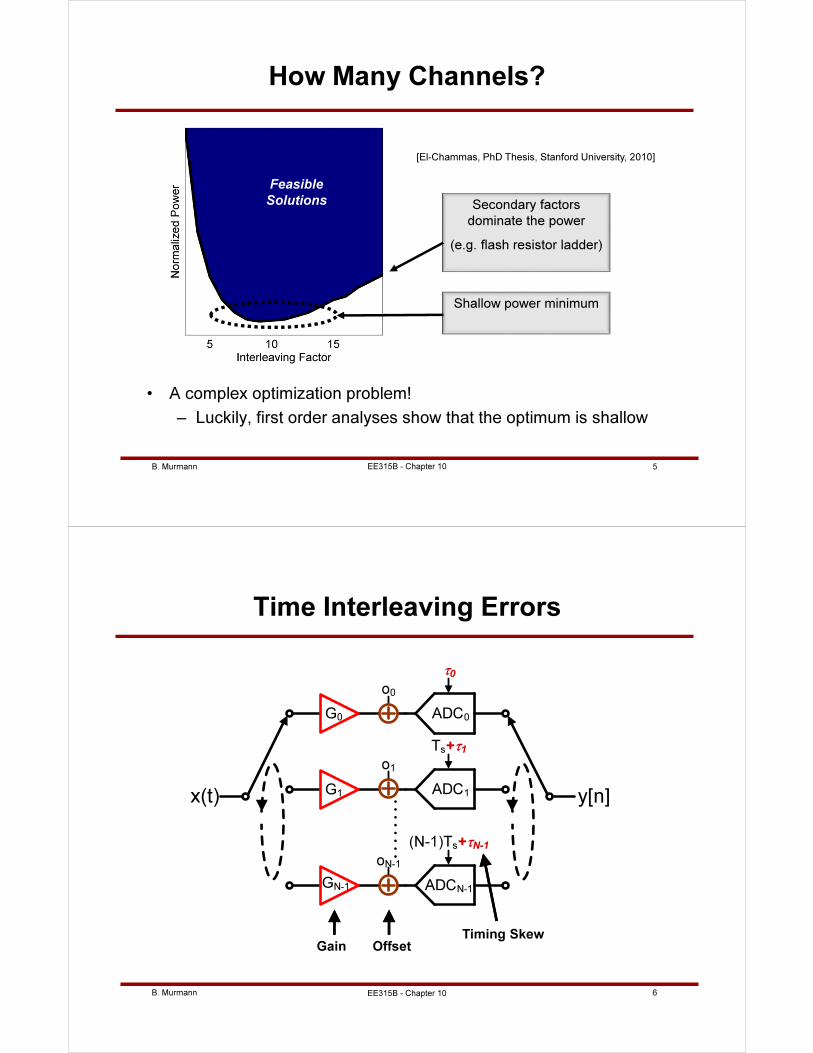
B. Murmann 5
How Many Channels?
• A complex optimization problem!
– Luckily, first order analyses show that the optimum is shallow
Feasible
Solutions
[El-Chammas, PhD Thesis, Stanford University, 2010]
Secondary factors
dominate the power
(e.g. flash resistor ladder)
Shallow power minimum
EE315B - Chapter 10
B. Murmann 6
τ0
x(t) y[n]
ADC0
Ts+τ1
ADC1
(N-1)Ts+τN-1
ADCN-1
G0
G1
GN-1
o0
o1
oN-1
Time Interleaving Errors
OffsetTiming Skew
Gain
EE315B - Chapter 10
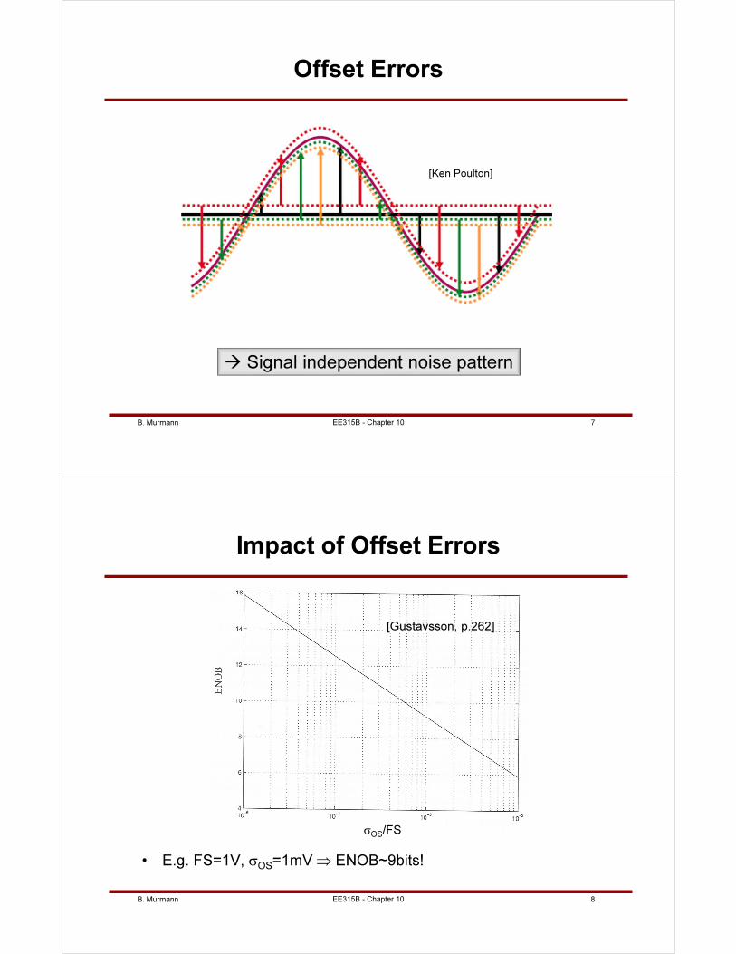
B. Murmann 7
Offset Errors
Signal independent noise pattern
[Ken Poulton]
EE315B - Chapter 10
B. Murmann 8EE315B - Chapter 10
Impact of Offset Errors
• E.g. FS=1V, σOS
=1mV ⇒ ENOB~9bits!
σOS/FS
[Gustavsson, p.262]
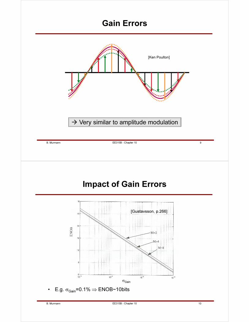
B. Murmann 9
Gain Errors
Very similar to amplitude modulation
[Ken Poulton]
EE315B - Chapter 10
B. Murmann 10EE315B - Chapter 10
Impact of Gain Errors
• E.g. σGain
=0.1% ⇒ ENOB~10bits
σGain
[Gustavsson, p.266]
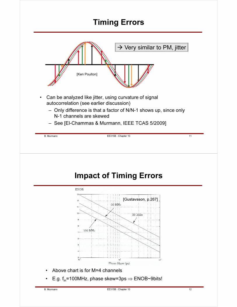
B. Murmann 11
Timing Errors
• Can be analyzed like jitter, using curvature of signal
autocorrelation (see earlier discussion)
– Only difference is that a factor of N/N-1 shows up, since only
N-1 channels are skewed
– See [El-Chammas & Murmann, IEEE TCAS 5/2009]
Very similar to PM, jitter
[Ken Poulton]
EE315B - Chapter 10
B. Murmann 12EE315B - Chapter 10
Impact of Timing Errors
• Above chart is for M=4 channels
• E.g. fin=100MHz, phase skew=3ps ⇒ ENOB~9bits!
[Gustavsson, p.267]
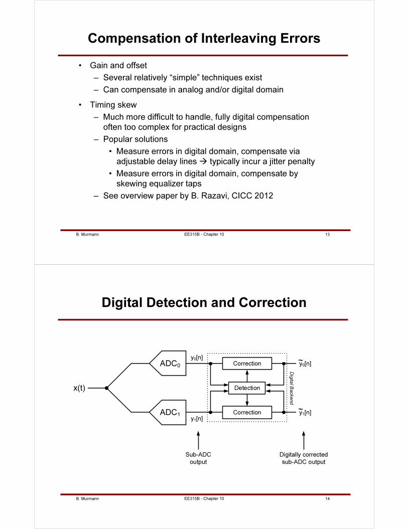
B. Murmann 13
Compensation of Interleaving Errors
• Gain and offset
– Several relatively “simple” techniques exist
– Can compensate in analog and/or digital domain
• Timing skew
– Much more difficult to handle, fully digital compensation
often too complex for practical designs
– Popular solutions
• Measure errors in digital domain, compensate via
adjustable delay lines typically incur a jitter penalty
• Measure errors in digital domain, compensate by
skewing equalizer taps
– See overview paper by B. Razavi, CICC 2012
EE315B - Chapter 10
B. Murmann 14
Digital Detection and Correction
Correction
Correction
Detection
ADC0
ADC1
y0[n]
y1[n]
y0[n]
y1[n]
x(t)
~
~
Sub-ADC
output
Digitally corrected
sub-ADC output
Dig
ital B
ackend
EE315B - Chapter 10
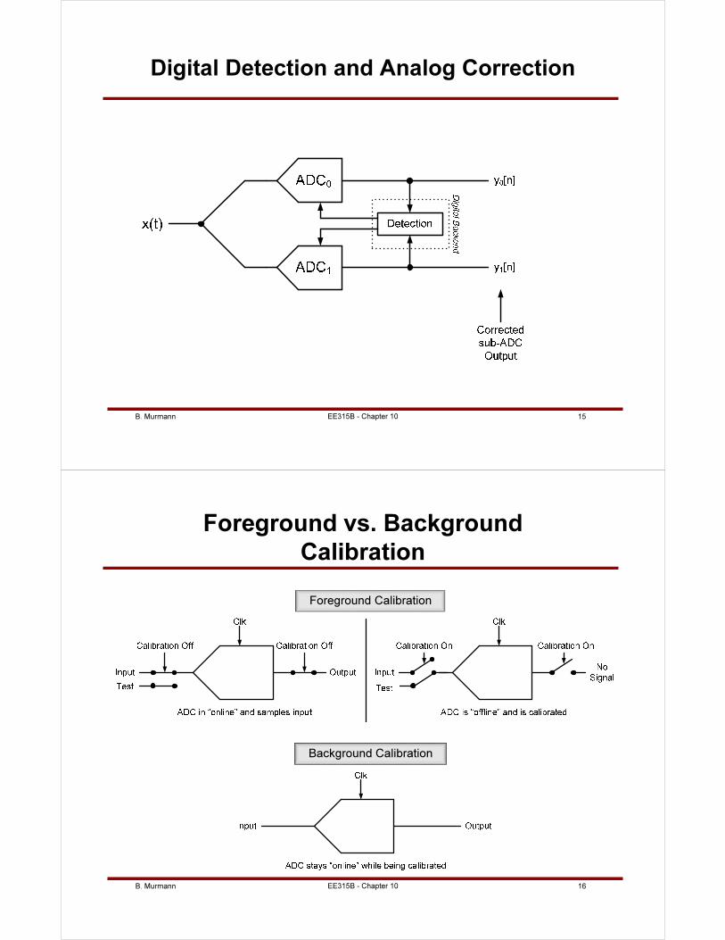
B. Murmann 15
Digital Detection and Analog Correction
EE315B - Chapter 10
B. Murmann 16
Foreground vs. Background
Calibration
Foreground Calibration
Background Calibration
EE315B - Chapter 10
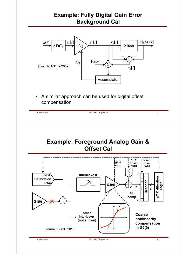
B. Murmann 17
Example: Fully Digital Gain Error
Background Cal
• A similar approach can be used for digital offset
compensation
[Tsai, TCAS1, 2/2009]
EE315B - Chapter 10
B. Murmann 18
Example: Foreground Analog Gain &
Offset Cal
G1(0)
6
µC
Ca
lib
rati
on
Lo
gic
8-bit
Calibration
DAC
63comp
Interleave 0
gain
cntrl
otherinterleave
(not shown)
De
co
de
r
G2(0)
5-bit
Coarse
nonlinearity
compensation
in G2(0)
offsetcntrl
comp offsetcntrl
vga
[Verma, ISSCC 2013]
Flash
EE315B - Chapter 10
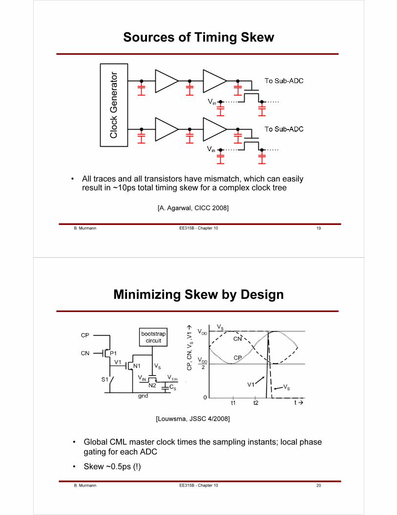
B. Murmann 19
Sources of Timing Skew
• All traces and all transistors have mismatch, which can easily result in ~10ps total timing skew for a complex clock tree
Clo
ck G
en
era
tor
[A. Agarwal, CICC 2008]
EE315B - Chapter 10
B. Murmann 20
Minimizing Skew by Design
• Global CML master clock times the sampling instants; local phase
gating for each ADC
• Skew ~0.5ps (!)
[Louwsma, JSSC 4/2008]
EE315B - Chapter 10
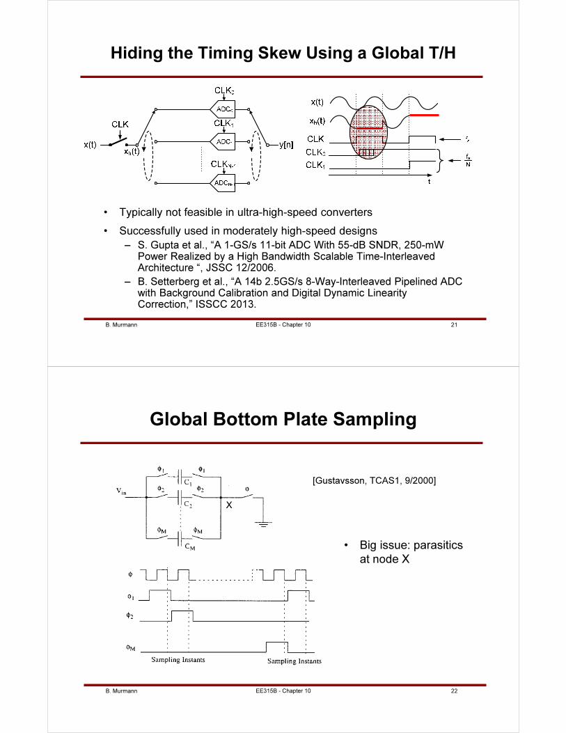
B. Murmann 21
Hiding the Timing Skew Using a Global T/H
• Typically not feasible in ultra-high-speed converters
• Successfully used in moderately high-speed designs
– S. Gupta et al., “A 1-GS/s 11-bit ADC With 55-dB SNDR, 250-mW Power Realized by a High Bandwidth Scalable Time-Interleaved Architecture “, JSSC 12/2006.
– B. Setterberg et al., “A 14b 2.5GS/s 8-Way-Interleaved Pipelined ADC with Background Calibration and Digital Dynamic Linearity Correction,” ISSCC 2013.
EE315B - Chapter 10
B. Murmann 22
Global Bottom Plate Sampling
• Big issue: parasitics
at node X
[Gustavsson, TCAS1, 9/2000]
X
EE315B - Chapter 10
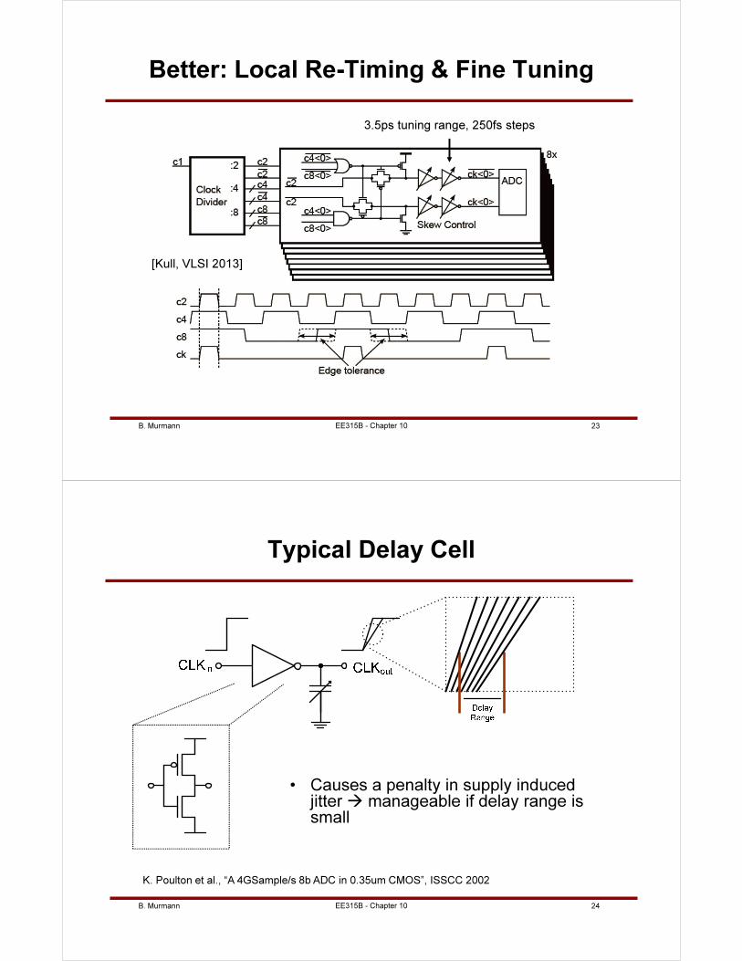
B. Murmann 23
Better: Local Re-Timing & Fine Tuning
[Kull, VLSI 2013]
3.5ps tuning range, 250fs steps
EE315B - Chapter 10
B. Murmann 24
Typical Delay Cell
• Causes a penalty in supply induced jitter manageable if delay range is small
K. Poulton et al., “A 4GSample/s 8b ADC in 0.35um CMOS”, ISSCC 2002
EE315B - Chapter 10
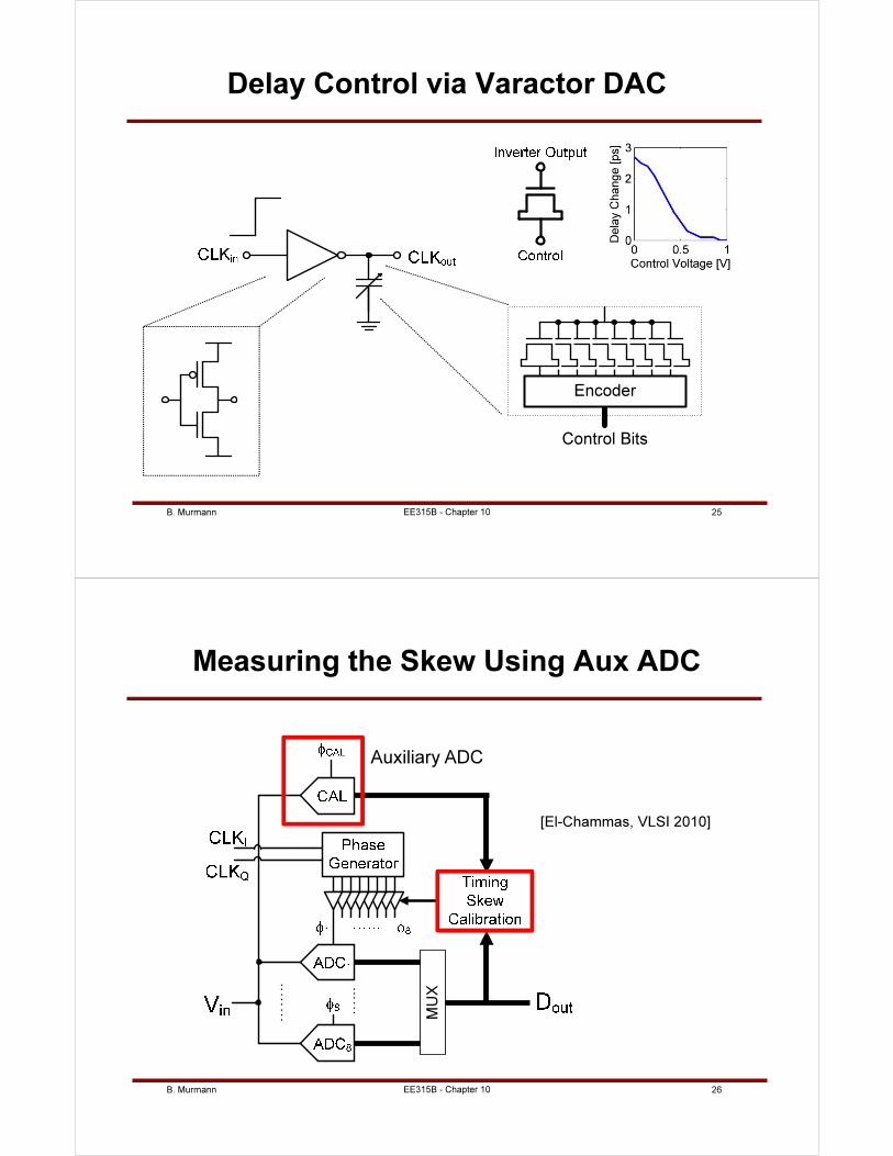
B. Murmann 25
Delay Control via Varactor DAC
Encoder
Control Bits
EE315B - Chapter 10
B. Murmann 26
Measuring the Skew Using Aux ADC
Auxiliary ADC
…...
……
..
MUX
[El-Chammas, VLSI 2010]
EE315B - Chapter 10
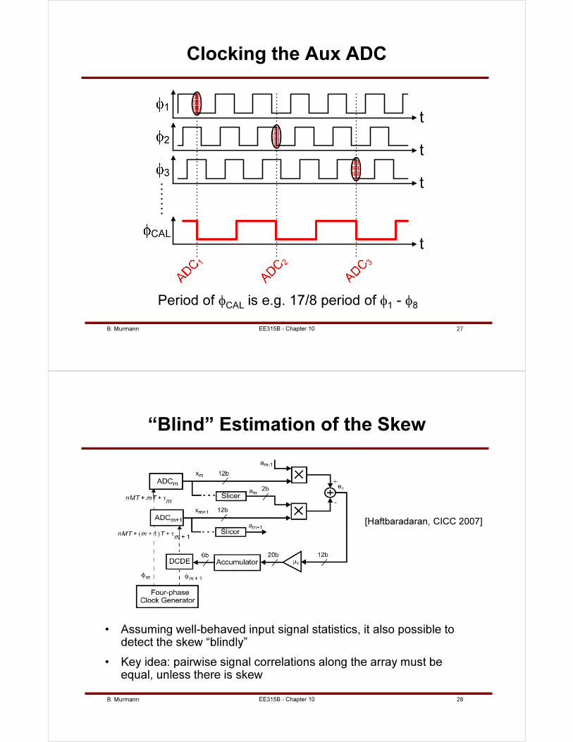
B. Murmann 27
Clocking the Aux ADC
1
1
2
3
CAL
t
t
t
t
2 3
Period of φCAL is e.g. 17/8 period of φ1 - φ8
EE315B - Chapter 10
B. Murmann 28
“Blind” Estimation of the Skew
• Assuming well-behaved input signal statistics, it also possible to detect the skew “blindly”
• Key idea: pairwise signal correlations along the array must be equal, unless there is skew
[Haftbaradaran, CICC 2007]
EE315B - Chapter 10
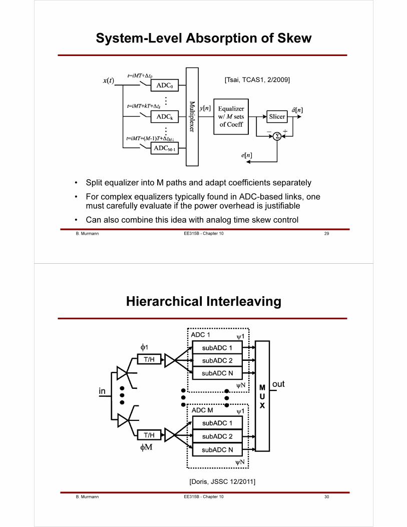
B. Murmann 29
System-Level Absorption of Skew
• Split equalizer into M paths and adapt coefficients separately
• For complex equalizers typically found in ADC-based links, one must carefully evaluate if the power overhead is justifiable
• Can also combine this idea with analog time skew control
[Tsai, TCAS1, 2/2009]
EE315B - Chapter 10
B. Murmann 30
Hierarchical Interleaving
[Doris, JSSC 12/2011]
EE315B - Chapter 10
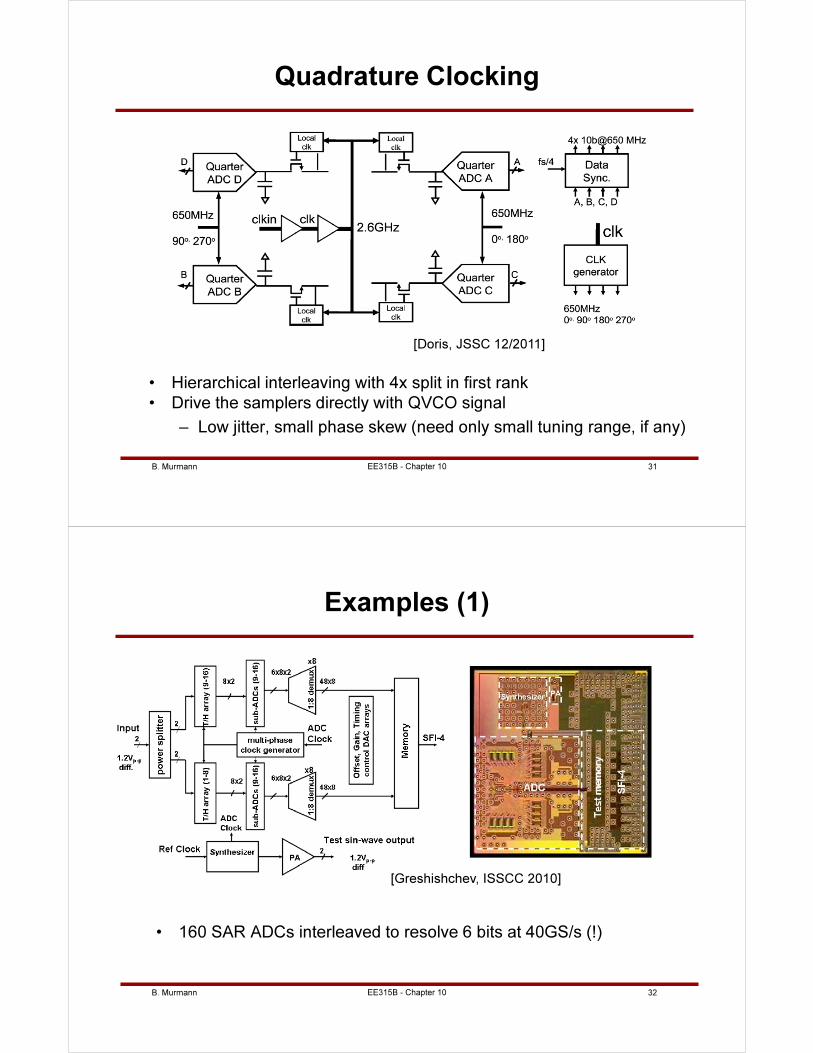
B. Murmann 31
Quadrature Clocking
• Hierarchical interleaving with 4x split in first rank
• Drive the samplers directly with QVCO signal
– Low jitter, small phase skew (need only small tuning range, if any)
[Doris, JSSC 12/2011]
EE315B - Chapter 10
B. Murmann 32
[Greshishchev, ISSCC 2010]
Examples (1)
• 160 SAR ADCs interleaved to resolve 6 bits at 40GS/s (!)
EE315B - Chapter 10
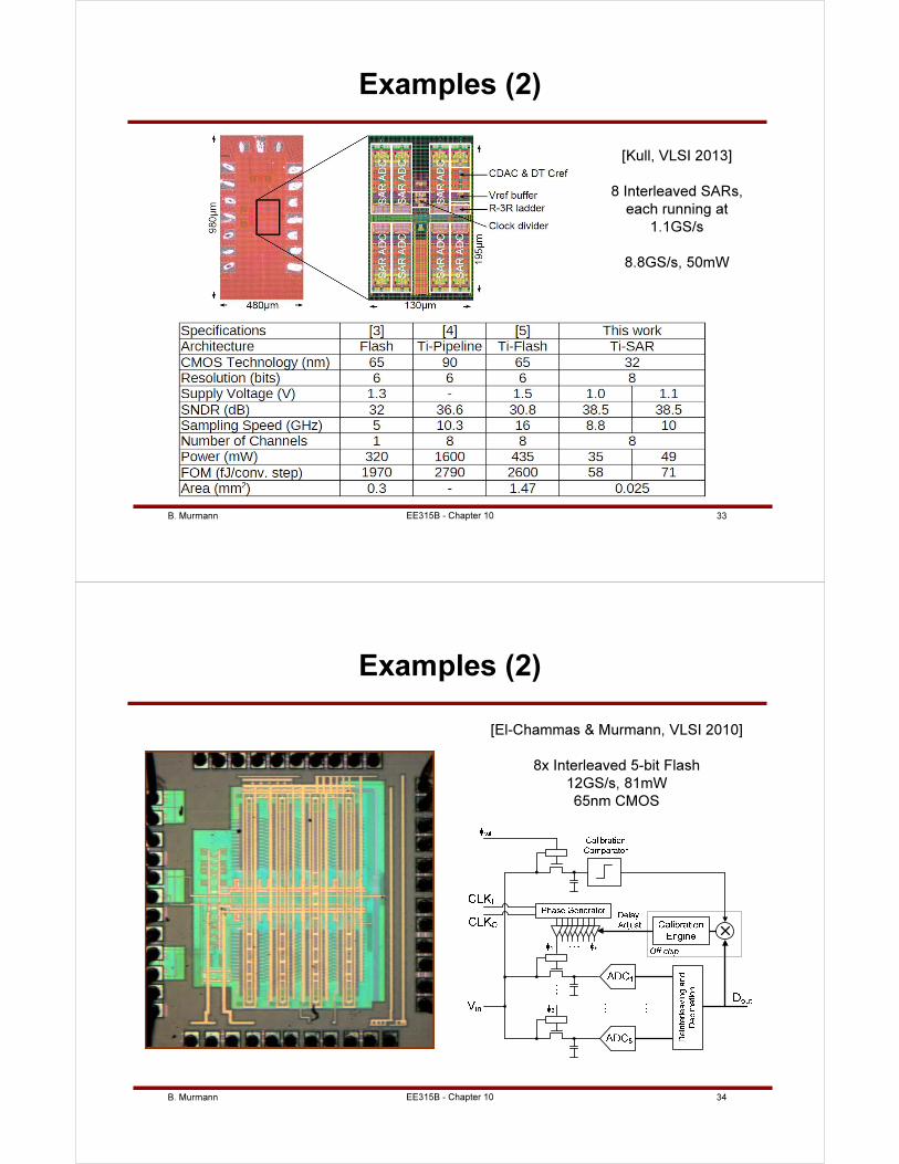
B. Murmann 33
Examples (2)
[Kull, VLSI 2013]
8 Interleaved SARs,
each running at
1.1GS/s
8.8GS/s, 50mW
EE315B - Chapter 10
B. Murmann 34
Examples (2)
[El-Chammas & Murmann, VLSI 2010]
8x Interleaved 5-bit Flash
12GS/s, 81mW
65nm CMOS
EE315B - Chapter 10
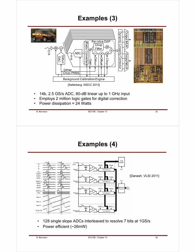
B. Murmann 35
Examples (3)
• 14b, 2.5 GS/s ADC, 80-dB linear up to 1 GHz input
• Employs 2 million logic gates for digital correction
• Power dissipation = 24 Watts
[Setterberg, ISSCC 2013]
EE315B - Chapter 10
B. Murmann 36
Examples (4)
• 128 single slope ADCs interleaved to resolve 7 bits at 1GS/s
• Power efficient (~26mW)
[Danesh, VLSI 2011]
EE315B - Chapter 10
B. Murmann 1EE315B - Chapter 11
Oversampling ADCs and DACs
Boris Murmann
Stanford University
Copyright © 2013 by Boris Murmann
B. Murmann 2
Overview
• Oversampling A/D conversion
• Decimation filters
• Oversampling D/A conversion
EE315B - Chapter 11
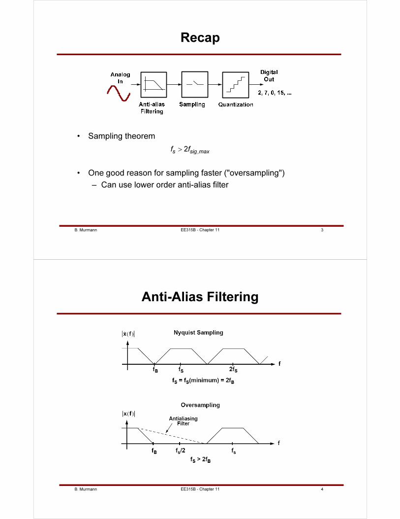
B. Murmann 3EE315B - Chapter 11
Recap
• Sampling theorem
2s sig,maxf f>
• One good reason for sampling faster ("oversampling")
– Can use lower order anti-alias filter
B. Murmann 4EE315B - Chapter 11
Anti-Alias Filtering
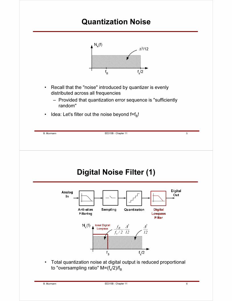
B. Murmann 5EE315B - Chapter 11
Quantization Noise
• Recall that the "noise" introduced by quantizer is evenly
distributed across all frequencies
– Provided that quantization error sequence is "sufficiently
random"
• Idea: Let's filter out the noise beyond f=fB!
fs/2
Ne(f)
∆2/12
fB
B. Murmann 6EE315B - Chapter 11
Digital Noise Filter (1)
• Total quantization noise at digital output is reduced proportional
to "oversampling ratio" M=(fs/2)/f
B
122/f
f 2
s
B∆⋅
12
2∆
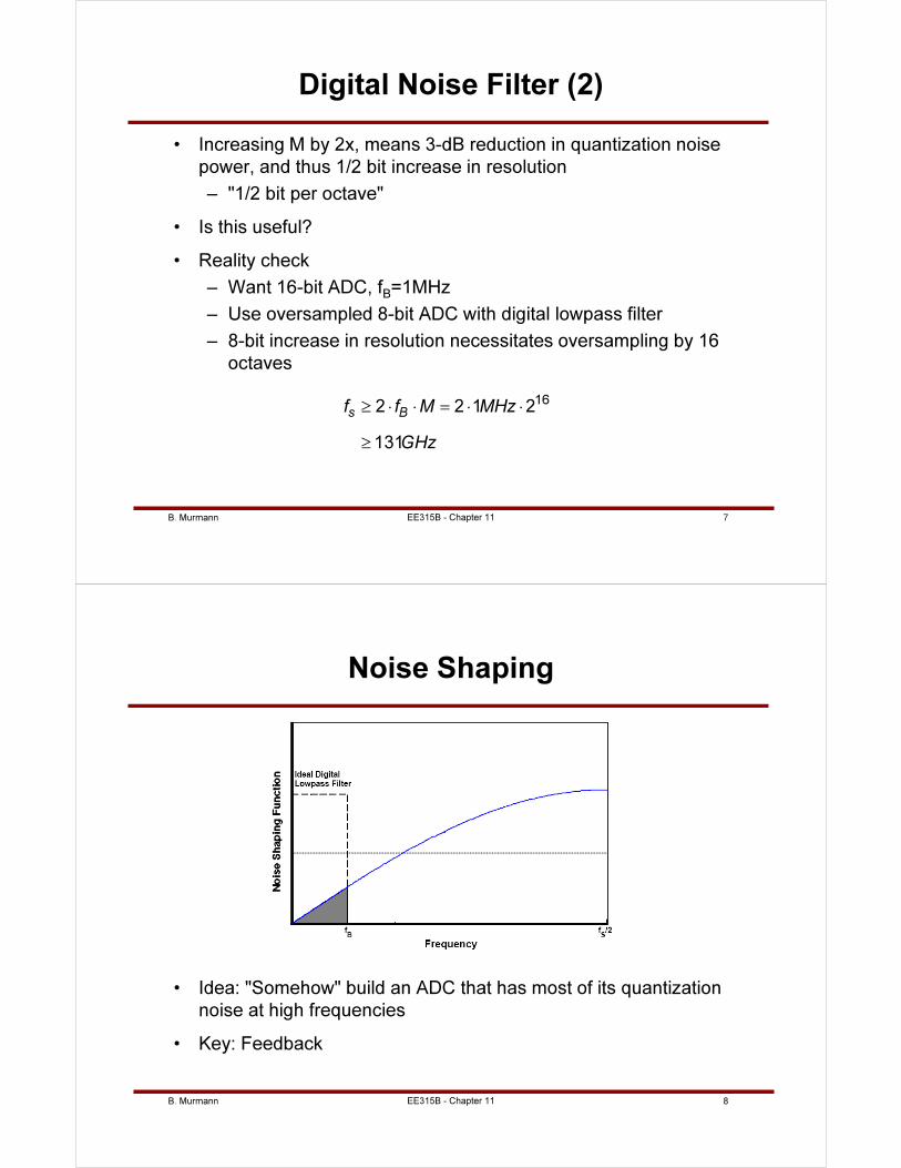
B. Murmann 7EE315B - Chapter 11
Digital Noise Filter (2)
• Increasing M by 2x, means 3-dB reduction in quantization noise
power, and thus 1/2 bit increase in resolution
– "1/2 bit per octave"
• Is this useful?
• Reality check
– Want 16-bit ADC, fB=1MHz
– Use oversampled 8-bit ADC with digital lowpass filter
– 8-bit increase in resolution necessitates oversampling by 16
octaves
162 2 1 2
131
s Bf f M MHz
GHz
≥ ⋅ ⋅ = ⋅ ⋅
≥
B. Murmann 8EE315B - Chapter 11
Noise Shaping
• Idea: "Somehow" build an ADC that has most of its quantization
noise at high frequencies
• Key: Feedback
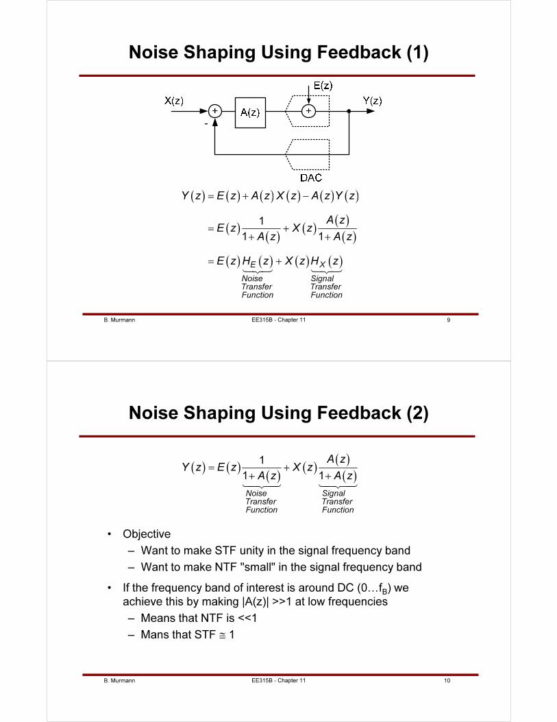
B. Murmann 9EE315B - Chapter 11
Noise Shaping Using Feedback (1)
( ) ( ) ( ) ( ) ( ) ( )
( )( )
( )( )
( )
( ) ( ) ( ) ( )
1
1 1
E X
Noise SignalTransfer TransferFunction Function
Y z E z A z X z A z Y z
A zE z X z
A z A z
E z H z X z H z
= + −
= +
+ +
= +
123 123
B. Murmann 10EE315B - Chapter 11
Noise Shaping Using Feedback (2)
• Objective
– Want to make STF unity in the signal frequency band
– Want to make NTF "small" in the signal frequency band
• If the frequency band of interest is around DC (0…fB) we
achieve this by making |A(z)| >>1 at low frequencies
– Means that NTF is <<1
– Mans that STF ≅ 1
( ) ( )( )
( )( )
( )1
1 1
Noise SignalTransfer TransferFunction Function
A zY z E z X z
A z A z= +
+ +
14243 14243
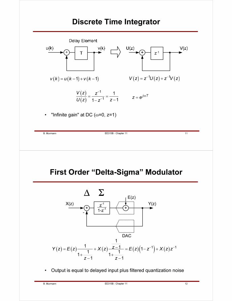
B. Murmann 11EE315B - Chapter 11
Discrete Time Integrator
• "Infinite gain" at DC (ω=0, z=1)
( ) ( ) ( )1 1v k u k v k= − + − ( ) ( ) ( )1 1V z z U z z V z
− −
= +
( )
( )
1
1
1
11
V z z
U z zz
−
−
= =
−−
j Tz e
ω
=
B. Murmann 12EE315B - Chapter 11
First Order “Delta-Sigma” Modulator
• Output is equal to delayed input plus filtered quantization noise
+
E(z)
X(z) Y(z)
DAC
+z-1
1-z-1
-
( ) ( ) ( ) ( ) ( ) ( )1 1
1
1 11
1 11 1
1 1
zY z E z X z E z z X z z
z z
− −−= + = − +
+ +
− −
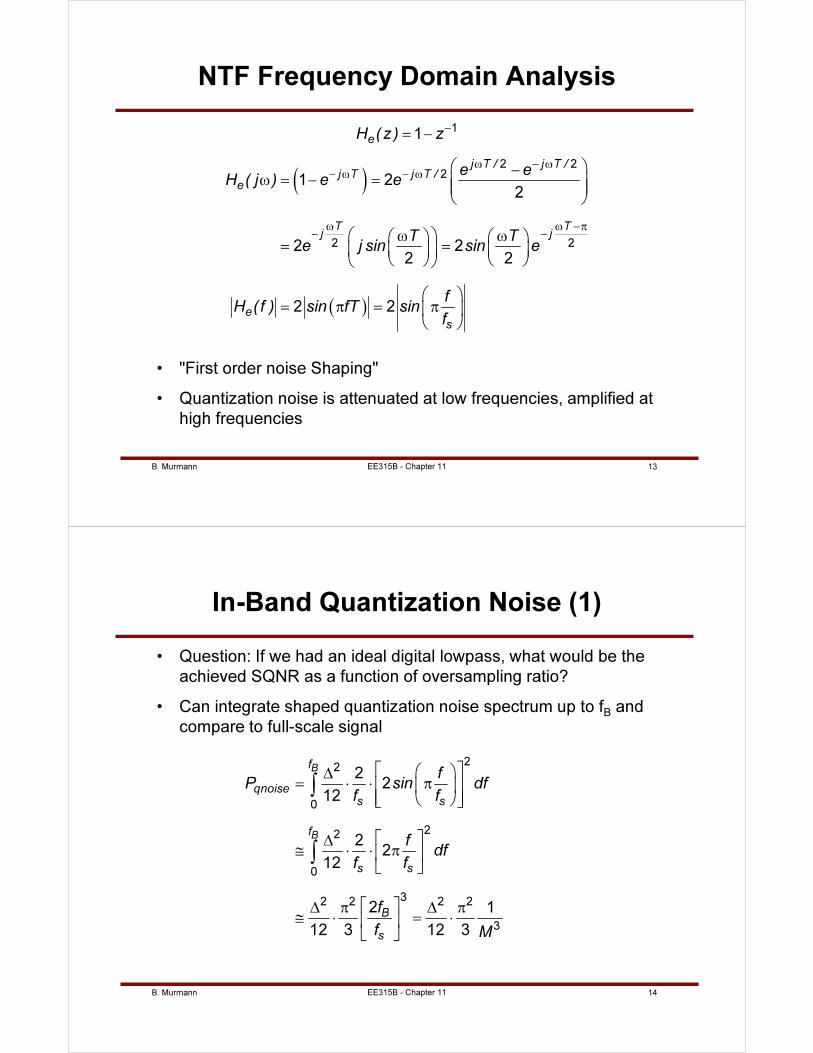
B. Murmann 13EE315B - Chapter 11
NTF Frequency Domain Analysis
• "First order noise Shaping"
• Quantization noise is attenuated at low frequencies, amplified at
high frequencies
11
eH (z) z−= −
( )
( )
2 22
2 2
1 22
2 22 2
2 2
j T / j T /j T j T /
e
T Tj j
es
e eH ( j ) e e
T Te j sin sin e
fH (f ) sin fT sin
f
ω − ω
− ω − ω
ω ω −π
− −
−ω = − =
ω ω = =
= π = π
B. Murmann 14EE315B - Chapter 11
In-Band Quantization Noise (1)
• Question: If we had an ideal digital lowpass, what would be the
achieved SQNR as a function of oversampling ratio?
• Can integrate shaped quantization noise spectrum up to fB
and
compare to full-scale signal
22
0
22
0
32 2 2 2
3
22
12
22
12
2 1
12 3 12 3
B
B
f
qnoises s
f
s s
B
s
fP sin df
f f
fdf
f f
f
f M
∆= ⋅ ⋅ π
∆≅ ⋅ ⋅ π
∆ π ∆ π≅ ⋅ = ⋅
∫
∫
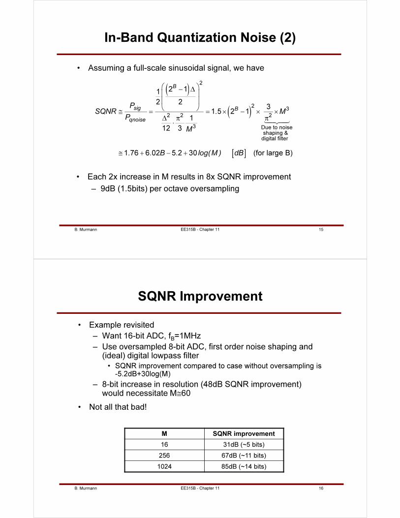
B. Murmann 15EE315B - Chapter 11
In-Band Quantization Noise (2)
• Assuming a full-scale sinusoidal signal, we have
( )
( )
[ ]
2
23
2 2 2
3 Due to noise shaping &digital filter
2 11
2 23
1 5 2 11
12 3
1 76 6 02 5 2 30 (for large B)
B
sig B
qnoise
PSQNR . M
P
M
. . B . log(M ) dB
− ∆ ≅ = = × − × ×∆ π π
⋅
≅ + − +
14243
• Each 2x increase in M results in 8x SQNR improvement
– 9dB (1.5bits) per octave oversampling
B. Murmann 16EE315B - Chapter 11
SQNR Improvement
M SQNR improvement
16 31dB (~5 bits)
256 67dB (~11 bits)
1024 85dB (~14 bits)
• Example revisited
– Want 16-bit ADC, fB=1MHz
– Use oversampled 8-bit ADC, first order noise shaping and (ideal) digital lowpass filter
• SQNR improvement compared to case without oversampling is -5.2dB+30log(M)
– 8-bit increase in resolution (48dB SQNR improvement) would necessitate M≅60
• Not all that bad!
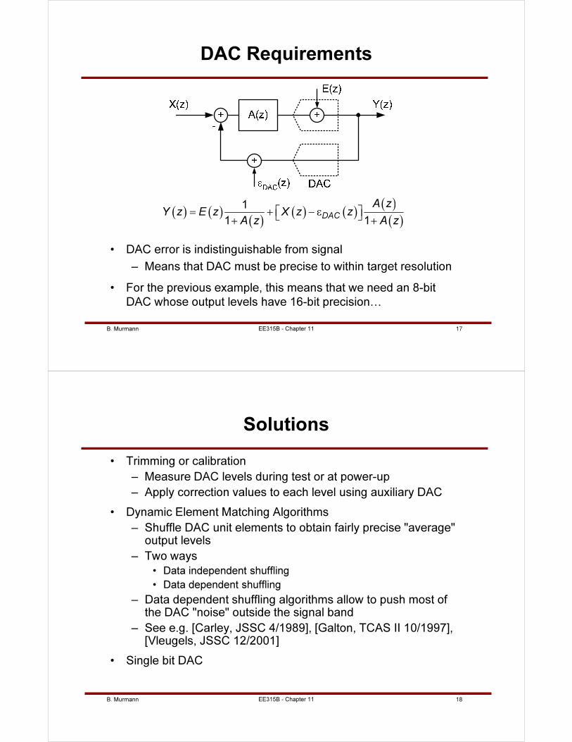
B. Murmann 17EE315B - Chapter 11
DAC Requirements
• DAC error is indistinguishable from signal
– Means that DAC must be precise to within target resolution
• For the previous example, this means that we need an 8-bit
DAC whose output levels have 16-bit precision…
( ) ( )( )
( ) ( )( )
( )1
1 1DAC
A zY z E z X z z
A z A z = + − ε + +
B. Murmann 18EE315B - Chapter 11
Solutions
• Trimming or calibration
– Measure DAC levels during test or at power-up
– Apply correction values to each level using auxiliary DAC
• Dynamic Element Matching Algorithms
– Shuffle DAC unit elements to obtain fairly precise "average" output levels
– Two ways
• Data independent shuffling
• Data dependent shuffling
– Data dependent shuffling algorithms allow to push most of the DAC "noise" outside the signal band
– See e.g. [Carley, JSSC 4/1989], [Galton, TCAS II 10/1997], [Vleugels, JSSC 12/2001]
• Single bit DAC
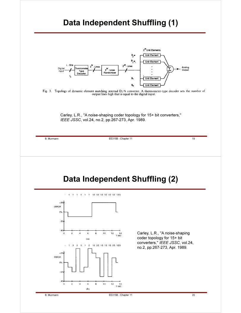
B. Murmann 19
Data Independent Shuffling (1)
EE315B - Chapter 11
Carley, L.R., "A noise-shaping coder topology for 15+ bit converters,"
IEEE JSSC, vol.24, no.2, pp.267-273, Apr. 1989.
B. Murmann 20
Data Independent Shuffling (2)
EE315B - Chapter 11
Carley, L.R., "A noise-shaping
coder topology for 15+ bit
converters," IEEE JSSC, vol.24,
no.2, pp.267-273, Apr. 1989.
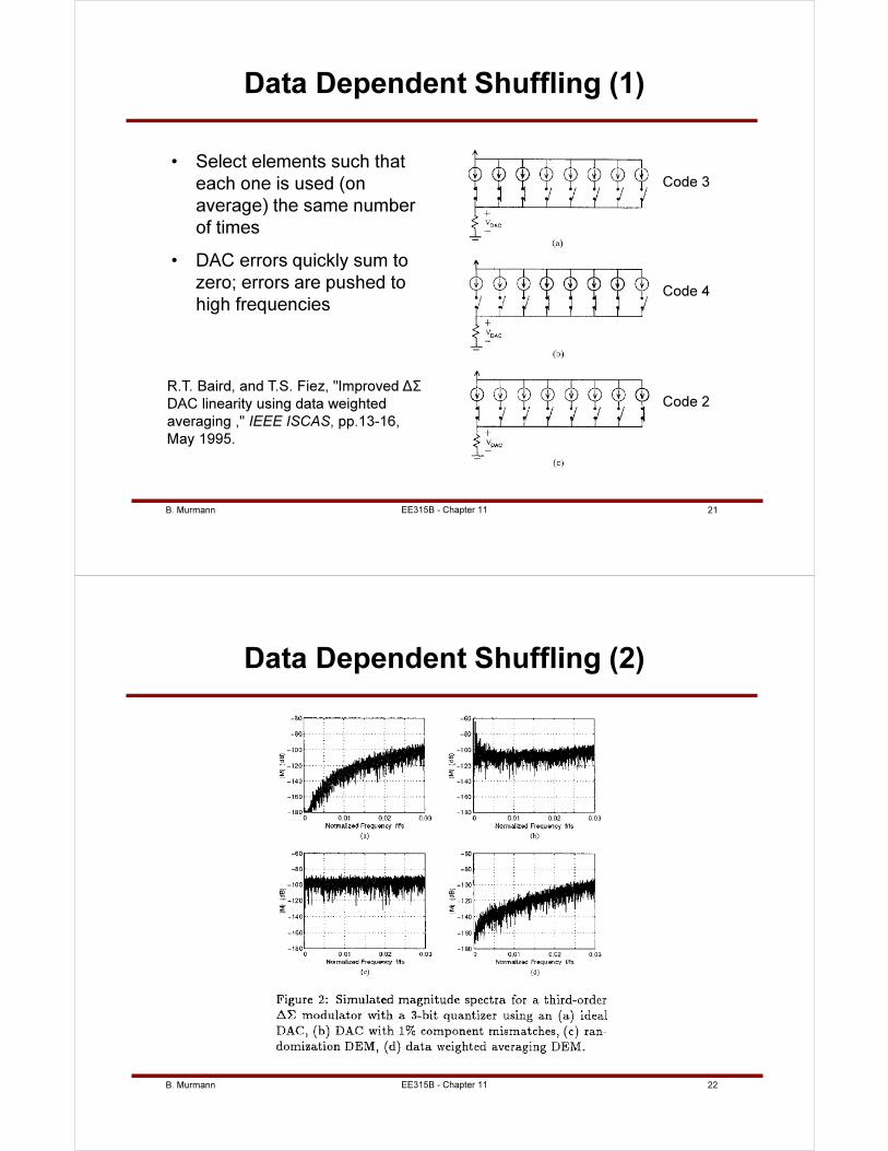
B. Murmann 21
Data Dependent Shuffling (1)
• Select elements such that
each one is used (on
average) the same number
of times
• DAC errors quickly sum to
zero; errors are pushed to
high frequencies
EE315B - Chapter 11
Code 3
Code 4
Code 2R.T. Baird, and T.S. Fiez, "Improved ΔΣ
DAC linearity using data weighted
averaging ," IEEE ISCAS, pp.13-16,
May 1995.
B. Murmann 22
Data Dependent Shuffling (2)
EE315B - Chapter 11
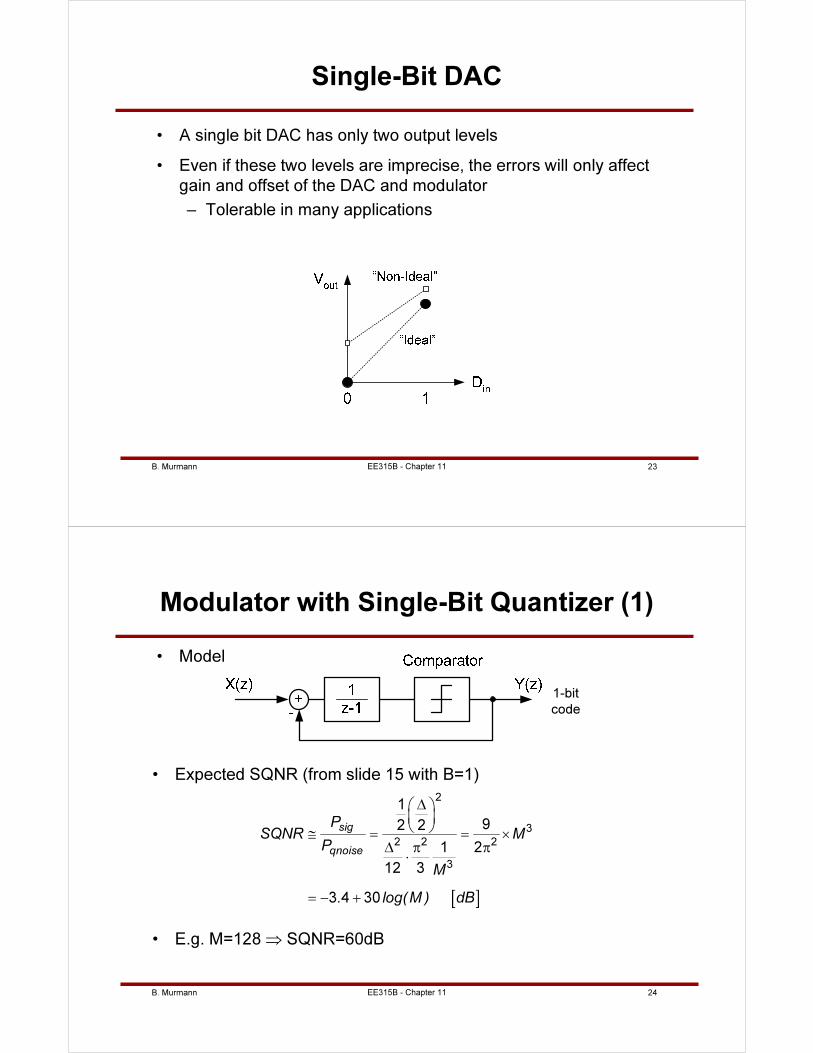
B. Murmann 23EE315B - Chapter 11
Single-Bit DAC
• A single bit DAC has only two output levels
• Even if these two levels are imprecise, the errors will only affect
gain and offset of the DAC and modulator
– Tolerable in many applications
B. Murmann 24EE315B - Chapter 11
Modulator with Single-Bit Quantizer (1)
• Model
• Expected SQNR (from slide 15 with B=1)
[ ]
2
3
2 2 2
3
1
92 2
1 2
12 3
3 4 30
sig
qnoise
PSQNR M
P
M
. log(M ) dB
∆ ≅ = = ×
∆ π π⋅
= − +
• E.g. M=128 ⇒ SQNR=60dB
1-bit
code
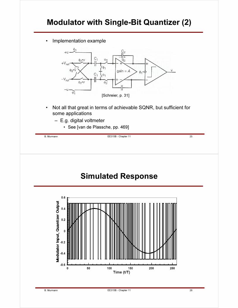
B. Murmann 25EE315B - Chapter 11
Modulator with Single-Bit Quantizer (2)
• Not all that great in terms of achievable SQNR, but sufficient for
some applications
– E.g. digital voltmeter
• See [van de Plassche, pp. 469]
[Schreier, p. 31]
• Implementation example
B. Murmann 26EE315B - Chapter 11
Simulated Response
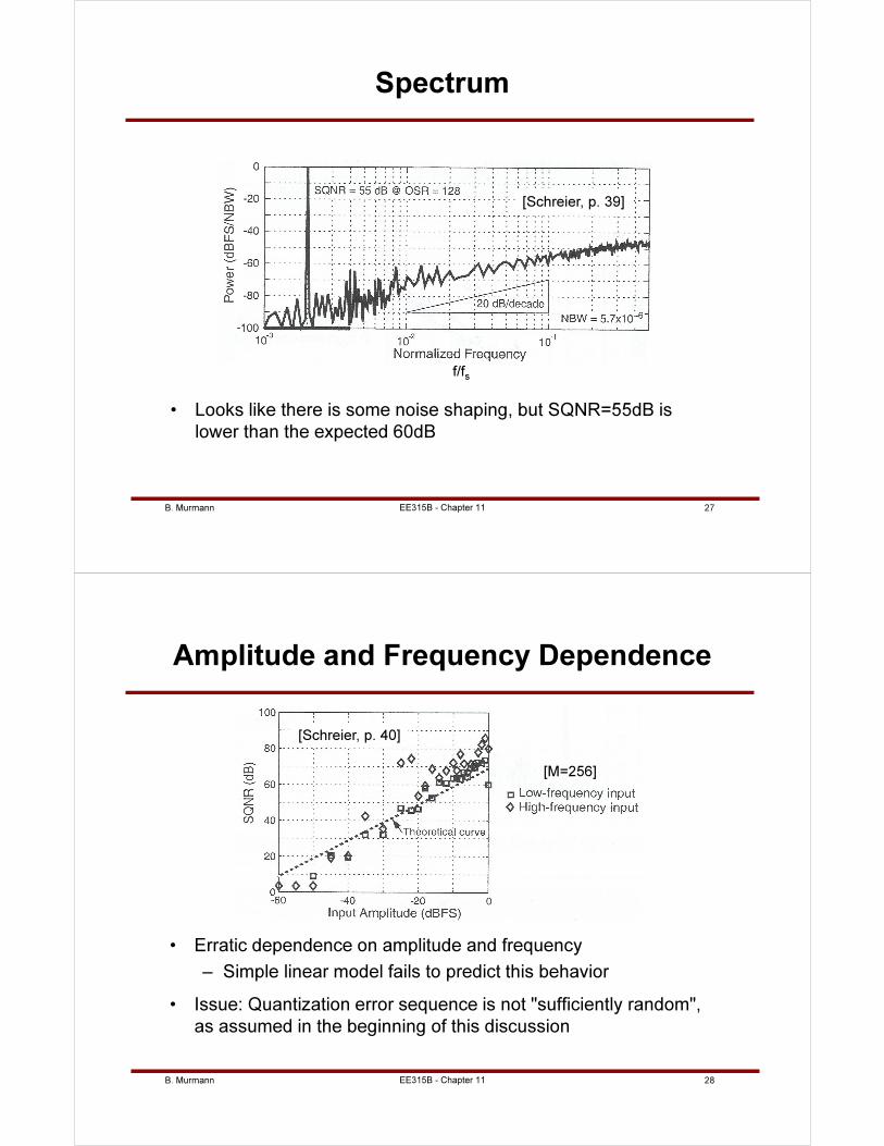
B. Murmann 27EE315B - Chapter 11
Spectrum
• Looks like there is some noise shaping, but SQNR=55dB is
lower than the expected 60dB
[Schreier, p. 39]
f/fs
B. Murmann 28EE315B - Chapter 11
Amplitude and Frequency Dependence
• Erratic dependence on amplitude and frequency
– Simple linear model fails to predict this behavior
• Issue: Quantization error sequence is not "sufficiently random",
as assumed in the beginning of this discussion
[Schreier, p. 40]
[M=256]
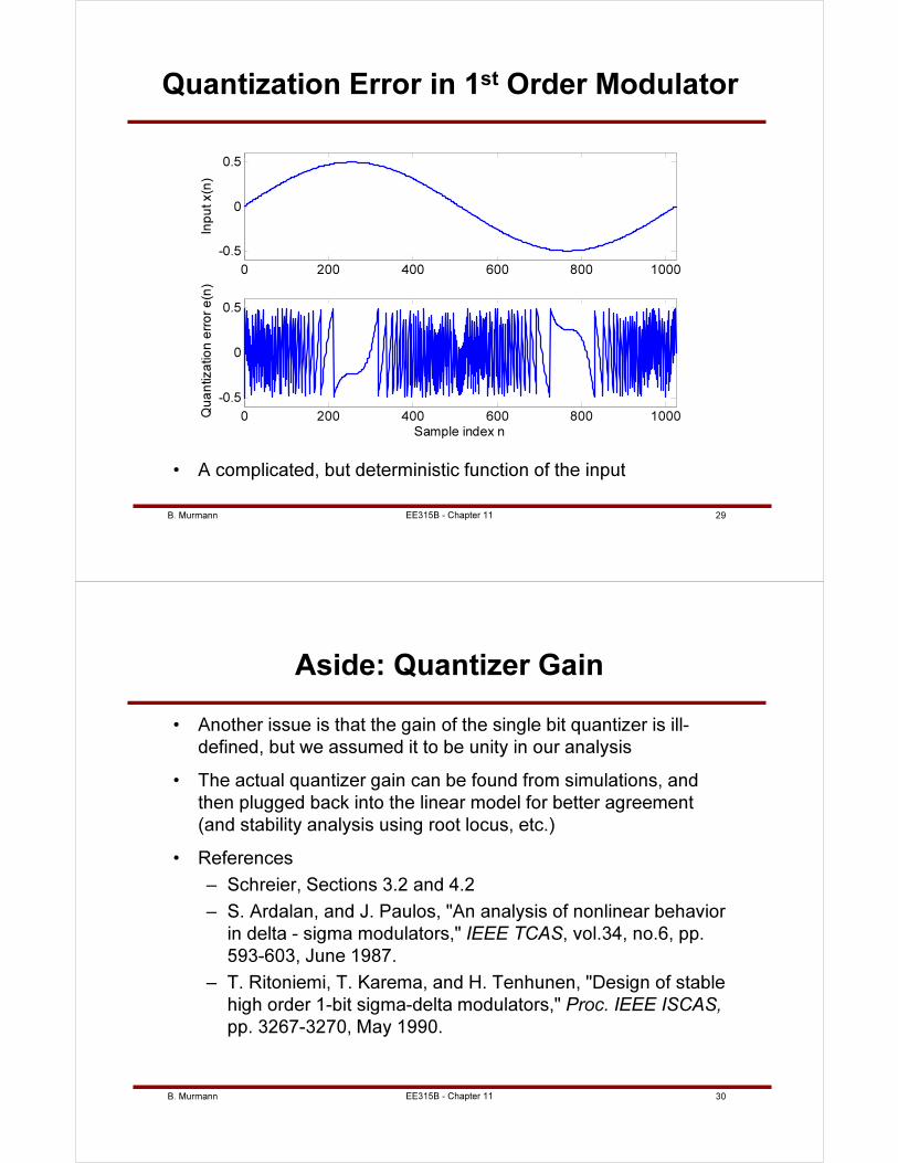
B. Murmann 29EE315B - Chapter 11
Quantization Error in 1st Order Modulator
• A complicated, but deterministic function of the input
0 200 400 600 800 1000
-0.5
0
0.5
Inp
ut x(n
)
0 200 400 600 800 1000
-0.5
0
0.5
Sample index n
Qu
an
tiza
tio
n e
rro
r e
(n)
B. Murmann 30
Aside: Quantizer Gain
• Another issue is that the gain of the single bit quantizer is ill-
defined, but we assumed it to be unity in our analysis
• The actual quantizer gain can be found from simulations, and
then plugged back into the linear model for better agreement
(and stability analysis using root locus, etc.)
• References
– Schreier, Sections 3.2 and 4.2
– S. Ardalan, and J. Paulos, "An analysis of nonlinear behavior
in delta - sigma modulators," IEEE TCAS, vol.34, no.6, pp.
593-603, June 1987.
– T. Ritoniemi, T. Karema, and H. Tenhunen, "Design of stable
high order 1-bit sigma-delta modulators," Proc. IEEE ISCAS,
pp. 3267-3270, May 1990.
EE315B - Chapter 11
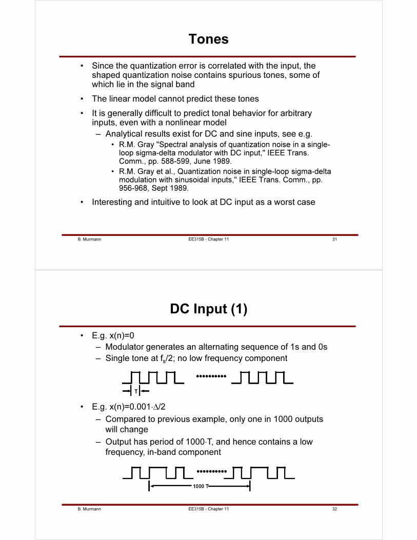
B. Murmann 31EE315B - Chapter 11
Tones
• Since the quantization error is correlated with the input, the shaped quantization noise contains spurious tones, some of which lie in the signal band
• The linear model cannot predict these tones
• It is generally difficult to predict tonal behavior for arbitrary inputs, even with a nonlinear model
– Analytical results exist for DC and sine inputs, see e.g.
• R.M. Gray "Spectral analysis of quantization noise in a single-loop sigma-delta modulator with DC input," IEEE Trans. Comm., pp. 588-599, June 1989.
• R.M. Gray et al., Quantization noise in single-loop sigma-delta modulation with sinusoidal inputs," IEEE Trans. Comm., pp. 956-968, Sept 1989.
• Interesting and intuitive to look at DC input as a worst case
B. Murmann 32EE315B - Chapter 11
DC Input (1)
• E.g. x(n)=0
– Modulator generates an alternating sequence of 1s and 0s
– Single tone at fs/2; no low frequency component
• E.g. x(n)=0.001⋅∆/2
– Compared to previous example, only one in 1000 outputs
will change
– Output has period of 1000⋅T, and hence contains a low
frequency, in-band component
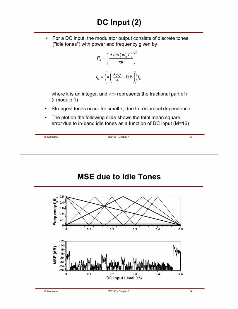
B. Murmann 33EE315B - Chapter 11
DC Input (2)
• For a DC input, the modulator output consists of discrete tones
("idle tones") with power and frequency given by
0 5DC
k s
xf k . f
= + ∆
where k is an integer, and <r> represents the fractional part of r
(r modulo 1)
• Strongest tones occur for small k, due to reciprocal dependence
• The plot on the following slide shows the total mean square
error due to in-band idle tones as a function of DC input (M=16)
( )2
k
k
sin f TP
k
∆ π=
π
B. Murmann 34EE315B - Chapter 11
MSE due to Idle Tones
X/∆

B. Murmann 35EE315B - Chapter 11
Idle Tone Considerations
• Idle tones are known to be a significant issue in audio applications
– The human ear can detect tones ~20dB below the
thermal/quantization noise floor
• If idle tones are an issue, there are several options for mitigating their
impact
– Larger oversampling ratio
– Multi-bit quantizer and DAC
– Dither
• Superimpose a pseudorandom signal at the quantizer input to "whiten"
quantization noise– See e.g. Chapter 3 of Delta-Sigma Data Converters by Norsworthy, Schreier & Temes.
– Overdesign by making quantization noise much smaller than
electronic noise from integrators
• Noisy integrator(s) help randomize quantization error sequence
– Higher order modulators
• Naturally produce "more random" quantization error sequences
B. Murmann 36EE315B - Chapter 11
Higher Order Modulators
• Motivation: better SQNR for a given oversampling ratio, plus
improved idle tone performance as a side benefit
• Commonly used architectures
– Single quantizer loop with higher order filtering
• Essentially a logical extension to the first order noise shaping
concept discussed previously
– Cascaded, multi-stage modulators
• Contain a separate quantizer in each stage
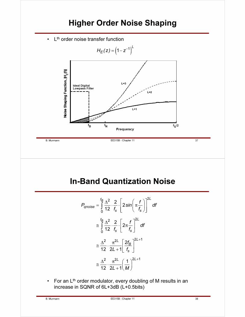
B. Murmann 37EE315B - Chapter 11
Higher Order Noise Shaping
• Lth order noise transfer function
( )11L
EH (z) z−= −
B. Murmann 38EE315B - Chapter 11
In-Band Quantization Noise
• For an Lth order modulator, every doubling of M results in an
increase in SQNR of 6L+3dB (L+0.5bits)
22
0
22
0
2 12 2
2 12 2
22
12
22
12
2
12 2 1
1
12 2 1
B
B
Lf
qnoises s
Lf
s s
LLB
s
LL
fP sin df
f f
fdf
f f
f
L f
L M
+
+
∆= ⋅ ⋅ π
∆≅ ⋅ ⋅ π
∆ π≅ ⋅
+
∆ π ≅ ⋅
+
∫
∫
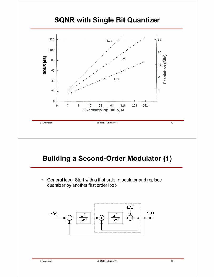
B. Murmann 39EE315B - Chapter 11
SQNR with Single Bit Quantizer
SQ
NR
[d
B]
B. Murmann 40
Building a Second-Order Modulator (1)
• General idea: Start with a first order modulator and replace
quantizer by another first order loop
EE315B - Chapter 11
-1
-1
-1
-1
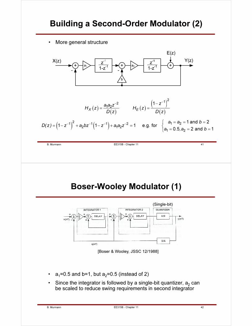
B. Murmann 41
Building a Second-Order Modulator (2)
• More general structure
EE315B - Chapter 11
+X(z) Y(z)z
1-z-+
E(z)
+z
1-z-
b
a1 a2
( )( )
( )( )
( )
( ) ( )
21
2
1 2
21 21 1 1 2
2 1 2
1 2
1
1 and 21 1 1 e.g. for
0 5 2 and 1
X E
za a zH z H z
D z D z
a a bD(z ) z a bz z a a z
a . ,a b
−
−
− − − −
−= =
= = == − + − + =
= = =
B. Murmann 42EE315B - Chapter 11
Boser-Wooley Modulator (1)
• a1=0.5 and b=1, but a
2=0.5 (instead of 2)
• Since the integrator is followed by a single-bit quantizer, a2
can be scaled to reduce swing requirements in second integrator
[Boser & Wooley, JSSC 12/1988]
(Single-bit)
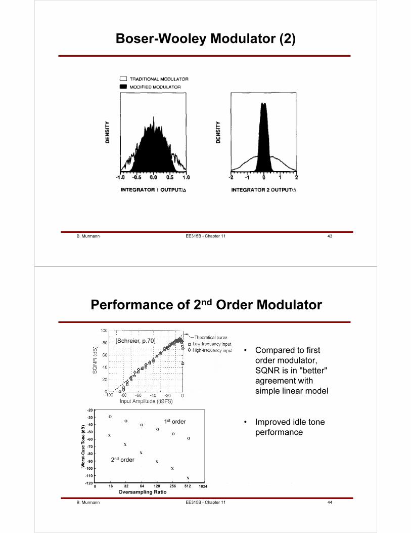
B. Murmann 43EE315B - Chapter 11
Boser-Wooley Modulator (2)
B. Murmann 44EE315B - Chapter 11
Performance of 2nd Order Modulator
• Compared to first
order modulator,
SQNR is in "better"
agreement with
simple linear model
[Schreier, p.70]
O
O
O
O
O
OX
X
X
X
X
X
-120
-110
-100
-90
-80
-70
-60
-50
-40
-30
-20
Oversampling Ratio
8 16 32 64 128 256 512 1024
1st order
2nd order
• Improved idle tone
performance
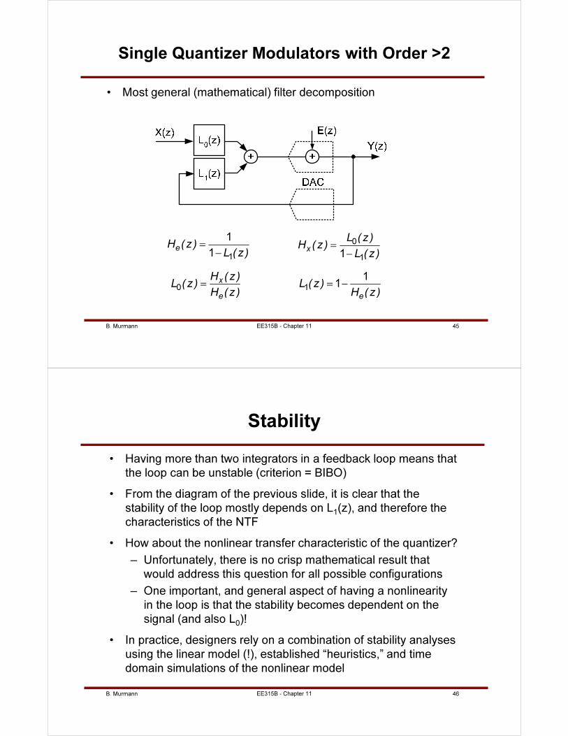
B. Murmann 45EE315B - Chapter 11
Single Quantizer Modulators with Order >2
1
1
1e
H (z)L ( z )
=
−
0
11x
L (z)H (z)
L ( z )=
−
0x
e
H (z)L ( z )
H (z )= 1
11
e
L (z)H (z )
= −
• Most general (mathematical) filter decomposition
B. Murmann 46
Stability
• Having more than two integrators in a feedback loop means that
the loop can be unstable (criterion = BIBO)
• From the diagram of the previous slide, it is clear that the
stability of the loop mostly depends on L1(z), and therefore the
characteristics of the NTF
• How about the nonlinear transfer characteristic of the quantizer?
– Unfortunately, there is no crisp mathematical result that
would address this question for all possible configurations
– One important, and general aspect of having a nonlinearity
in the loop is that the stability becomes dependent on the
signal (and also L0)!
• In practice, designers rely on a combination of stability analyses
using the linear model (!), established “heuristics,” and time
domain simulations of the nonlinear model
EE315B - Chapter 11
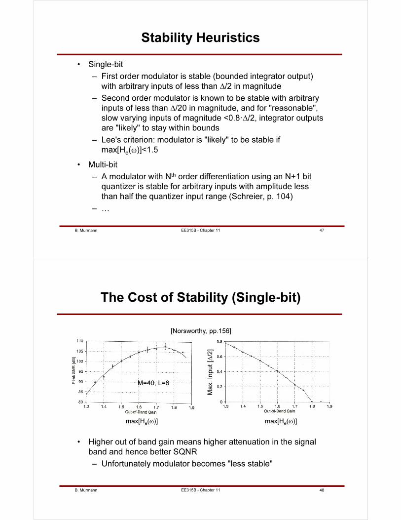
B. Murmann 47EE315B - Chapter 11
Stability Heuristics
• Single-bit
– First order modulator is stable (bounded integrator output)
with arbitrary inputs of less than ∆/2 in magnitude
– Second order modulator is known to be stable with arbitrary
inputs of less than ∆/20 in magnitude, and for "reasonable",
slow varying inputs of magnitude <0.8·∆/2, integrator outputs
are "likely" to stay within bounds
– Lee's criterion: modulator is "likely" to be stable if
max[He(ω)]<1.5
• Multi-bit
– A modulator with Nth order differentiation using an N+1 bit
quantizer is stable for arbitrary inputs with amplitude less
than half the quantizer input range (Schreier, p. 104)
– …
B. Murmann 48EE315B - Chapter 11
The Cost of Stability (Single-bit)
• Higher out of band gain means higher attenuation in the signal
band and hence better SQNR
– Unfortunately modulator becomes "less stable"
Ma
x.
Inp
ut
[∆/2
]
[Norsworthy, pp.156]
M=40, L=6
max[He(ω)]max[H
e(ω)]
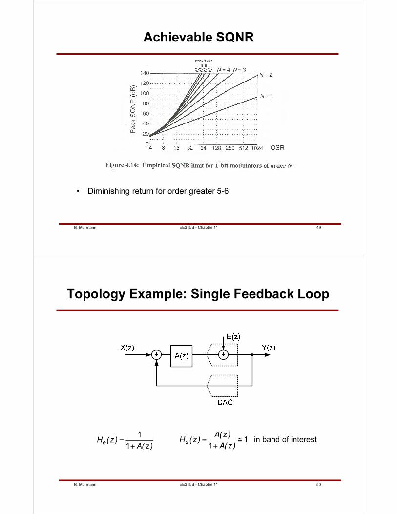
B. Murmann 49EE315B - Chapter 11
Achievable SQNR
• Diminishing return for order greater 5-6
B. Murmann 50EE315B - Chapter 11
Topology Example: Single Feedback Loop
1
1e
H (z)A(z )
=
+
1 in band of interest1
x
A(z )H (z )
A(z )= ≅
+
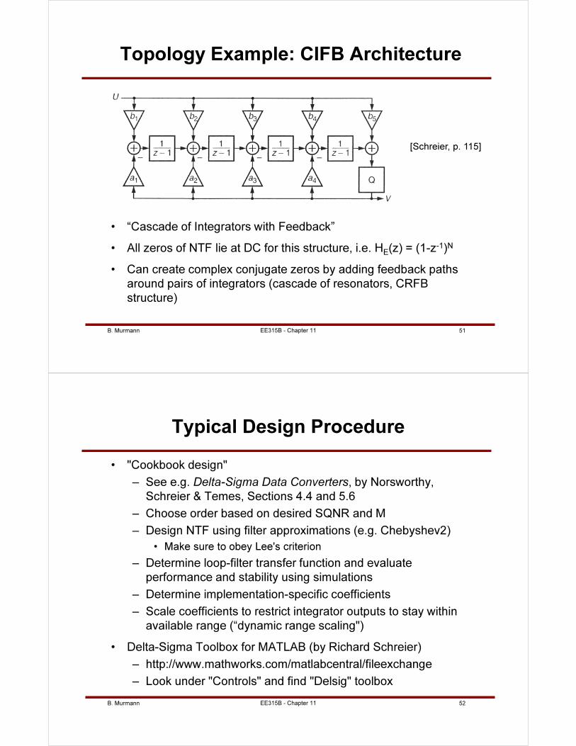
B. Murmann 51
Topology Example: CIFB Architecture
• “Cascade of Integrators with Feedback”
• All zeros of NTF lie at DC for this structure, i.e. HE(z) = (1-z-1)N
• Can create complex conjugate zeros by adding feedback paths
around pairs of integrators (cascade of resonators, CRFB
structure)
EE315B - Chapter 11
[Schreier, p. 115]
B. Murmann 52EE315B - Chapter 11
Typical Design Procedure
• "Cookbook design"
– See e.g. Delta-Sigma Data Converters, by Norsworthy,
Schreier & Temes, Sections 4.4 and 5.6
– Choose order based on desired SQNR and M
– Design NTF using filter approximations (e.g. Chebyshev2)
• Make sure to obey Lee's criterion
– Determine loop-filter transfer function and evaluate
performance and stability using simulations
– Determine implementation-specific coefficients
– Scale coefficients to restrict integrator outputs to stay within
available range (“dynamic range scaling")
• Delta-Sigma Toolbox for MATLAB (by Richard Schreier)
– http://www.mathworks.com/matlabcentral/fileexchange
– Look under "Controls" and find "Delsig" toolbox
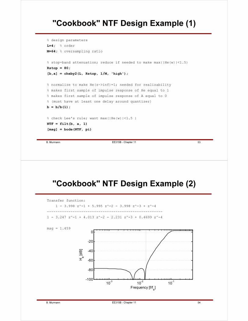
B. Murmann 53EE315B - Chapter 11
"Cookbook" NTF Design Example (1)
% design parameters
L=4; % order
M=64; % oversampling ratio
% stop-band attenuation; reduce if needed to make max(|He(w)|<1.5)
Rstop = 80;
[b,a] = cheby2(L, Rstop, 1/M, 'high');
% normalize to make He(z->inf)=1; needed for realizability
% makes first sample of impulse response of He equal to 1
% makes first sample of impulse response of A equal to 0
% (must have at least one delay around quantizer)
b = b/b(1);
% check Lee's rule; want max(|He(w)|<1.5 )
NTF = filt(b, a, 1)
[mag] = bode(NTF, pi)
B. Murmann 54EE315B - Chapter 11
"Cookbook" NTF Design Example (2)
Transfer function:
1 - 3.998 z^-1 + 5.995 z^-2 - 3.998 z^-3 + z^-4
------------------------------------------------------
1 - 3.247 z^-1 + 4.013 z^-2 - 2.231 z^-3 + 0.4699 z^-4
mag = 1.459
10-3
10-2
10-1
-100
-80
-60
-40
-20
0
Frequency [f/fs]
He [d
B]
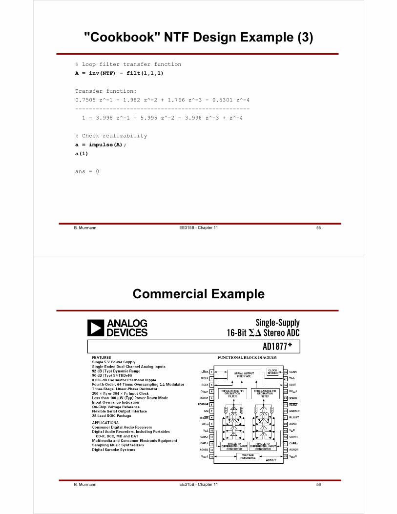
B. Murmann 55EE315B - Chapter 11
"Cookbook" NTF Design Example (3)
% Loop filter transfer function
A = inv(NTF) - filt(1,1,1)
Transfer function:
0.7505 z^-1 - 1.982 z^-2 + 1.766 z^-3 - 0.5301 z^-4
---------------------------------------------------
1 - 3.998 z^-1 + 5.995 z^-2 - 3.998 z^-3 + z^-4
% Check realizability
a = impulse(A);
a(1)
ans = 0
B. Murmann 56EE315B - Chapter 11
Commercial Example
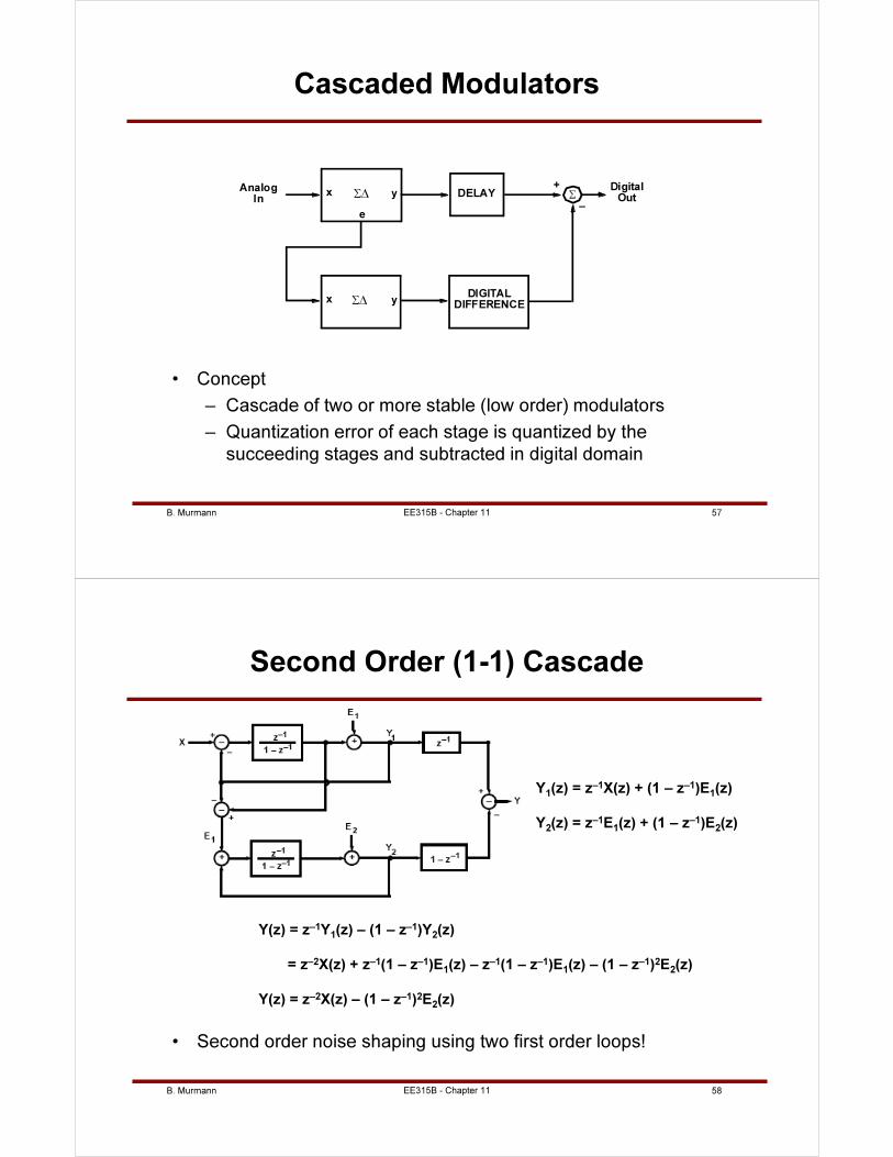
B. Murmann 57EE315B - Chapter 11
Cascaded Modulators
• Concept
– Cascade of two or more stable (low order) modulators
– Quantization error of each stage is quantized by the
succeeding stages and subtracted in digital domain
Σx
e
y DELAY
x y
+
–
DIGITALDIFFERENCE
Σ∆
Σ∆
DigitalOut
AnalogIn
B. Murmann 58EE315B - Chapter 11
Second Order (1-1) Cascade
• Second order noise shaping using two first order loops!
Y(z) = z–1Y1(z) – (1 – z–1)Y
2(z)
= z–2X(z) + z–1(1 – z–1)E1(z) – z–1(1 – z–1)E
1(z) – (1 – z–1)2E
2(z)
Y(z) = z–2X(z) – (1 – z–1)2E2(z)
Y1(z) = z–1X(z) + (1 – z–1)E
1(z)
Y2(z) = z–1E
1(z) + (1 – z–1)E
2(z)
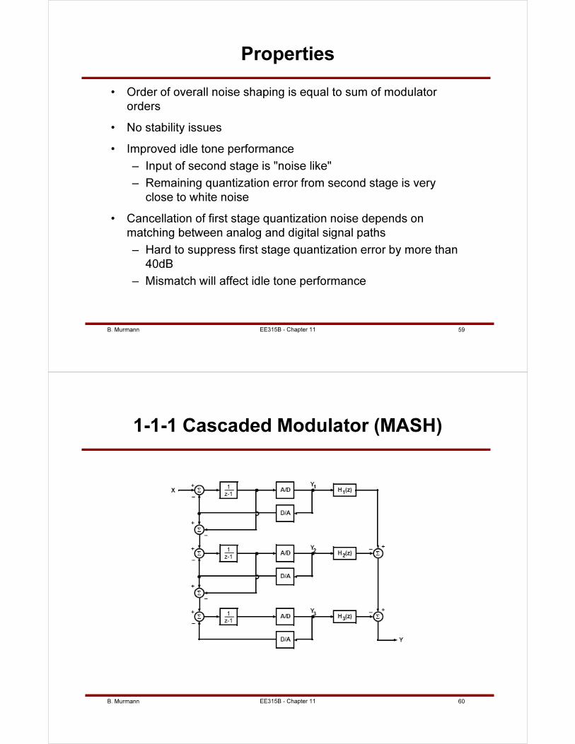
B. Murmann 59EE315B - Chapter 11
Properties
• Order of overall noise shaping is equal to sum of modulator
orders
• No stability issues
• Improved idle tone performance
– Input of second stage is "noise like"
– Remaining quantization error from second stage is very
close to white noise
• Cancellation of first stage quantization noise depends on
matching between analog and digital signal paths
– Hard to suppress first stage quantization error by more than
40dB
– Mismatch will affect idle tone performance
B. Murmann 60EE315B - Chapter 11
1-1-1 Cascaded Modulator (MASH)
1
z-1
1
z-1
1
z-1
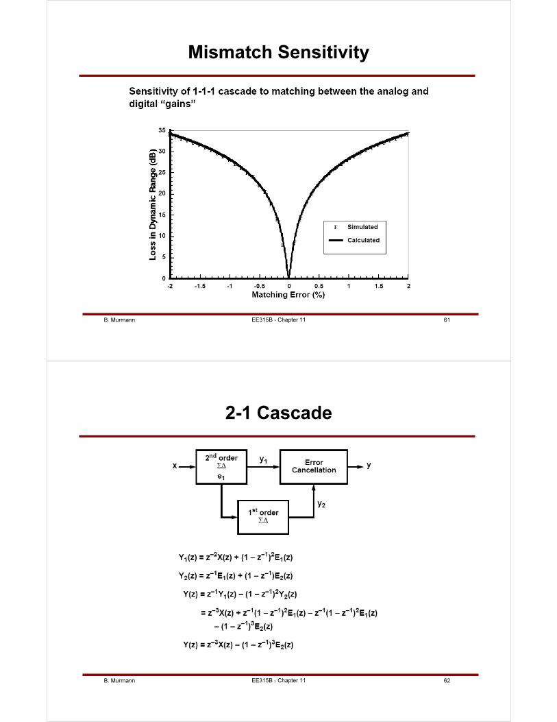
B. Murmann 61EE315B - Chapter 11
Mismatch Sensitivity
B. Murmann 62EE315B - Chapter 11
2-1 Cascade
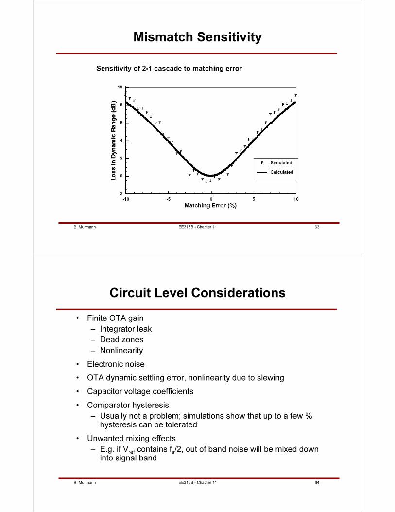
B. Murmann 63EE315B - Chapter 11
Mismatch Sensitivity
B. Murmann 64EE315B - Chapter 11
Circuit Level Considerations
• Finite OTA gain
– Integrator leak
– Dead zones
– Nonlinearity
• Electronic noise
• OTA dynamic settling error, nonlinearity due to slewing
• Capacitor voltage coefficients
• Comparator hysteresis
– Usually not a problem; simulations show that up to a few % hysteresis can be tolerated
• Unwanted mixing effects
– E.g. if Vref
contains fs/2, out of band noise will be mixed down
into signal band
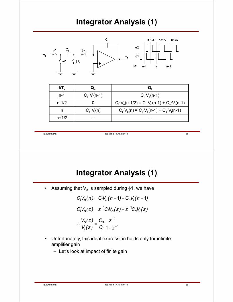
B. Murmann 65EE315B - Chapter 11
Integrator Analysis (1)
t/Ts Qs QI
n-1 Cs·V
i(n-1) C
I·V
o(n-1)
n-1/2 0 CI·V
o(n-1/2) = C
I·V
o(n-1) + C
s·V
i(n-1)
n Cs·V
i(n) C
I·V
o(n) = C
I·V
o(n-1) + C
s·V
i(n-1)
n+1/2 … …
B. Murmann 66EE315B - Chapter 11
Integrator Analysis (1)
• Assuming that Vo
is sampled during φ1, we have
1 1
1
1
1 1
1
I o I o s i
I o I o s i
o s
i I
CV (n ) CV (n ) C V (n )
CV (z) z CV (z ) z C V (z )
V (z ) C z
V (z ) C z
− −
−
−
= − + −
= +
∴ =
−
• Unfortunately, this ideal expression holds only for infinite
amplifier gain
– Let's look at impact of finite gain
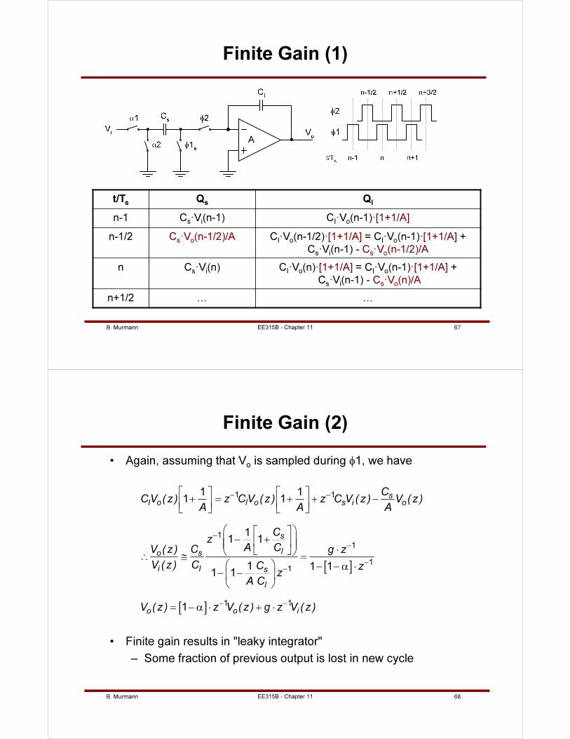
B. Murmann 67EE315B - Chapter 11
Finite Gain (1)
t/Ts Qs QI
n-1 Cs·V
i(n-1) C
I·V
o(n-1)·[1+1/A]
n-1/2 Cs·V
o(n-1/2)/A C
I·V
o(n-1/2)·[1+1/A] = C
I·V
o(n-1)·[1+1/A] +
Cs·V
i(n-1) - C
s·V
o(n-1/2)/A
n Cs·V
i(n) C
I·V
o(n)·[1+1/A] = C
I·V
o(n-1)·[1+1/A] +
Cs·V
i(n-1) - C
s·V
o(n)/A
n+1/2 … …
A
B. Murmann 68EE315B - Chapter 11
Finite Gain (2)
• Again, assuming that Vo
is sampled during φ1, we have
[ ]
[ ]
1 1
1
1
11
1 1
1 11 1
11 1
1 1 11 1
1
sI o I o s i o
s
Io s
i I s
I
o o i
CCV (z) z CV (z ) z C V (z) V (z )
A A A
Cz
A CV (z) C g z
V (z) C C zz
A C
V (z ) z V (z ) g z V (z )
− −
−
−
−
−
− −
+ = + + −
− + ⋅ ∴ ≅ =
− − α ⋅− −
= − α ⋅ + ⋅
• Finite gain results in "leaky integrator"
– Some fraction of previous output is lost in new cycle
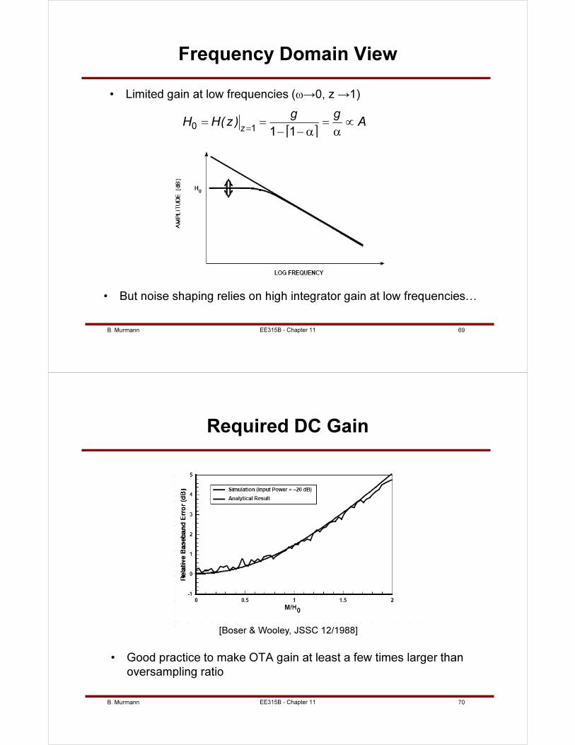
B. Murmann 69EE315B - Chapter 11
Frequency Domain View
• Limited gain at low frequencies (ω→0, z →1)
[ ]0 1 1 1z
g gH H(z) A
=
= = = ∝
− − α α
• But noise shaping relies on high integrator gain at low frequencies…
B. Murmann 70EE315B - Chapter 11
Required DC Gain
• Good practice to make OTA gain at least a few times larger than
oversampling ratio
[Boser & Wooley, JSSC 12/1988]
B. Murmann 71
Integrator Noise
• Noise splits into an input referred and output referred component
– The two noise components are correlated
– Luckily, only the input referred component is relevant
• We’ll see that output noise is first-order shaped by the modulator
EE315B - Chapter 11
[Schreier, TCAS1, 2005]
B. Murmann 72
Integrator’s Input Referred Noise
EE315B - Chapter 11
2in,tot
s s s
kT kT 1 kT 1v
1C C C 1 x1
x
= + + αγ+
+
14444244443
m onx g 2R= ⋅
Analysis of phi2 noise:
Calculate noise charge left behind
at Y after switch has turned off.
Charges at X and Y are equal and
opposite, so calculating charge on
Cs
accomplishes the task.
[Schreier, TCAS1, 2005]φ1
φ2
B. Murmann 73
Second-Order ∆Σ Modulator
PSD(f)
fs/2
f
2in,tot1v
PSD(f)
fs/2
f
2in,tot2v
( )1 1Y(z)2 1 z z
N2(z)
− −
= −2Y(z)
zN1(z)
−
=
EE315B - Chapter 11
B. Murmann 74
In-Band Noise
PSD(f)
fs/2
f
PSD(f)
fs/2
f
+
fs/2
ffb
Digital filter
PSD(f)
fs/2
f
PSD(f)
fs/2
f
+
s
b
f / 2OSR
f=
fb
fb
EE315B - Chapter 11
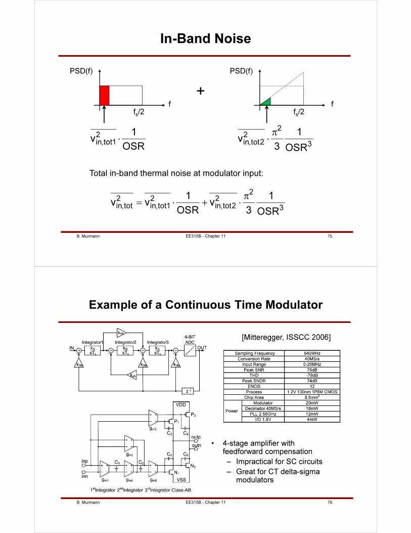
B. Murmann 75
In-Band Noise
PSD(f)
fs/2
f
PSD(f)
fs/2
f
+
2in,tot1
1v
OSR⋅
22in,tot2 3
1v
3 OSR
π
⋅
22 2 2in,tot in,tot1 in,tot2 3
1 1v v v
OSR 3 OSR
π= ⋅ + ⋅
Total in-band thermal noise at modulator input:
EE315B - Chapter 11
B. Murmann 76EE315B - Chapter 11
Example of a Continuous Time Modulator
[Mitteregger, ISSCC 2006]
• 4-stage amplifier with feedforward compensation
– Impractical for SC circuits
– Great for CT delta-sigma modulators
B. Murmann 77EE315B - Chapter 11
Multi-Mode Modulator
[Ouzounov, ISSCC 2007]
• Delta-sigma ADCs are
more amenable to BW
and DR reconfiguration
– Very hard to
reconfigure pipelined
ADCs
• Great for flexible, multi-
standard wireless
receivers
B. Murmann 78EE315B - Chapter 11
Decimation Filters
• References
– J. Candy, "Decimation for Sigma-Delta Modulation," IEEE Trans. Communications, pp. 72-76, Jan. 1986.
– Chapters 1 and 13 of Delta-Sigma Data Converters, by Norsworthy, Schreier, Temes.
– B.P. Brandt and B.A. Wooley, "A low-power, area-efficient digital filter for decimation and interpolation," IEEE J. Solid-State Circuits, pp. 679-687, June 1994.
– E. Hogenauer, "An economical class of digital filters for decimation and interpolation," IEEE Trans. Acoustics, Speech and Signal Processing, pp. 155-162, Apr 1981.
• Objectives
– Remove out-of band quantization noise
– Re-sample at lower frequency
• Ideally at Nyquist rate
B. Murmann 79EE315B - Chapter 11
Example
• Filter must attenuate spectral components around ± N·fN,
– Otherwise they will alias onto signal after re-sampling
Decimation Filter (M = 256)
Σ∆ Modulator
(2nd-Order)
Analog Input
Digital Output (16 Bits)
fN
44.1 kHz
11.3 MHz
1-Bit
11.3 MHz
fS
FrequencyFrequencyFrequency
Signal
Noise
Quantization Noise
B. Murmann 80EE315B - Chapter 11
Filter Requirements
• Pass band 0…20kHz, transition band 20…24.1kHz (∆f=4.1kHz),
stop band 24.1kHz…5.65MHz
• A digital FIR filter that meets these requirements would require
more than fs/∆f = 11.3MHz/4.1kHz ≅ 2800 coefficients
– Impractical!
B. Murmann 81EE315B - Chapter 11
Multi-Step Decimation
• Key idea: Don’t try to decimate down to fN
in one step
– Perform a gradual reduction of sampling rate + some filtering
– E.g. Two-step decimation
• Example: M1=64, f
s/M
1=176.4kHz
B. Murmann 82EE315B - Chapter 11
Sinc Filter (1)
• A popular, low complexity choice for stage 1 is the so-called sinc-filter
• From a time domain perspective, this filter simply computes the average of several samples
( )1
0
1N
i
y(n ) x n iN
−
=
= −∑
• Frequency domain
1
1 1
1
NzH(z )
N z
−
−
−
=
−
( )11
s
fj N
s f
s
fsin N
fH( ) e
fN
f
− π −
π
ω =π
• Zeros at multiples of fs/N
– Make N=M1
to attenuate alias components!
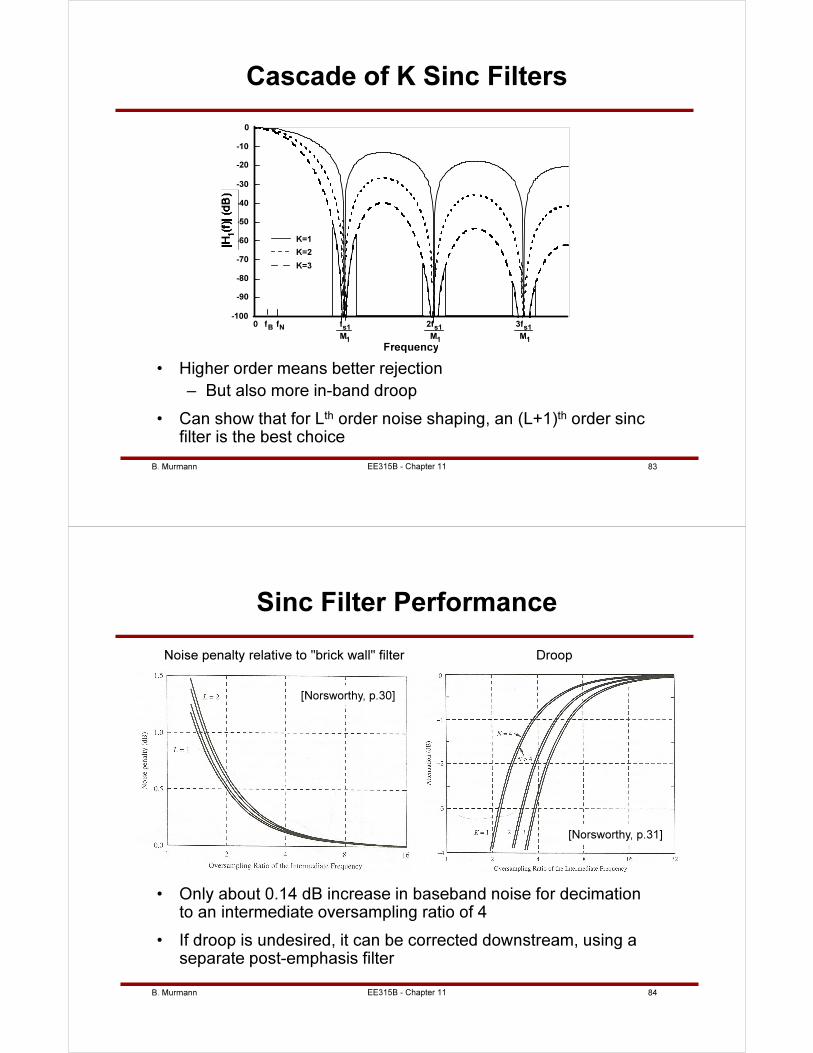
B. Murmann 83EE315B - Chapter 11
Cascade of K Sinc Filters
• Higher order means better rejection
– But also more in-band droop
• Can show that for Lth order noise shaping, an (L+1)th order sinc filter is the best choice
-100
-90
-80
-70
-60
-50
-40
-30
-20
-10
0
Frequency
0 2fs1
M1
fs1
M1
fN
fB
3fs1
M1
K=1
K=2
K=3
B. Murmann 84EE315B - Chapter 11
Sinc Filter Performance
• Only about 0.14 dB increase in baseband noise for decimation to an intermediate oversampling ratio of 4
• If droop is undesired, it can be corrected downstream, using a separate post-emphasis filter
Noise penalty relative to "brick wall" filter Droop
[Norsworthy, p.30]
[Norsworthy, p.31]
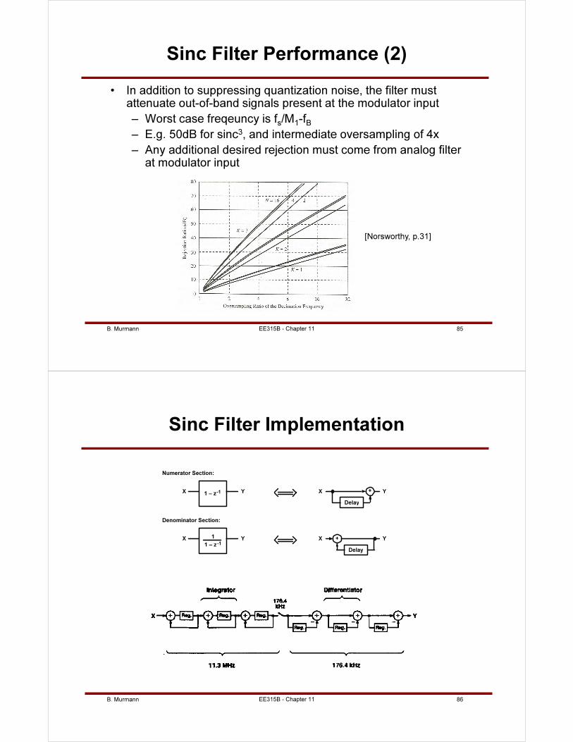
B. Murmann 85EE315B - Chapter 11
Sinc Filter Performance (2)
• In addition to suppressing quantization noise, the filter must attenuate out-of-band signals present at the modulator input
– Worst case freqeuncy is fs/M
1-fB
– E.g. 50dB for sinc3, and intermediate oversampling of 4x
– Any additional desired rejection must come from analog filter at modulator input
[Norsworthy, p.31]
B. Murmann 86EE315B - Chapter 11
Sinc Filter Implementation
X Y1 – z-1
Numerator Section:
X Y1 – z-1
Denominator Section:
1
X Y+
Delay
X Y+
Delay
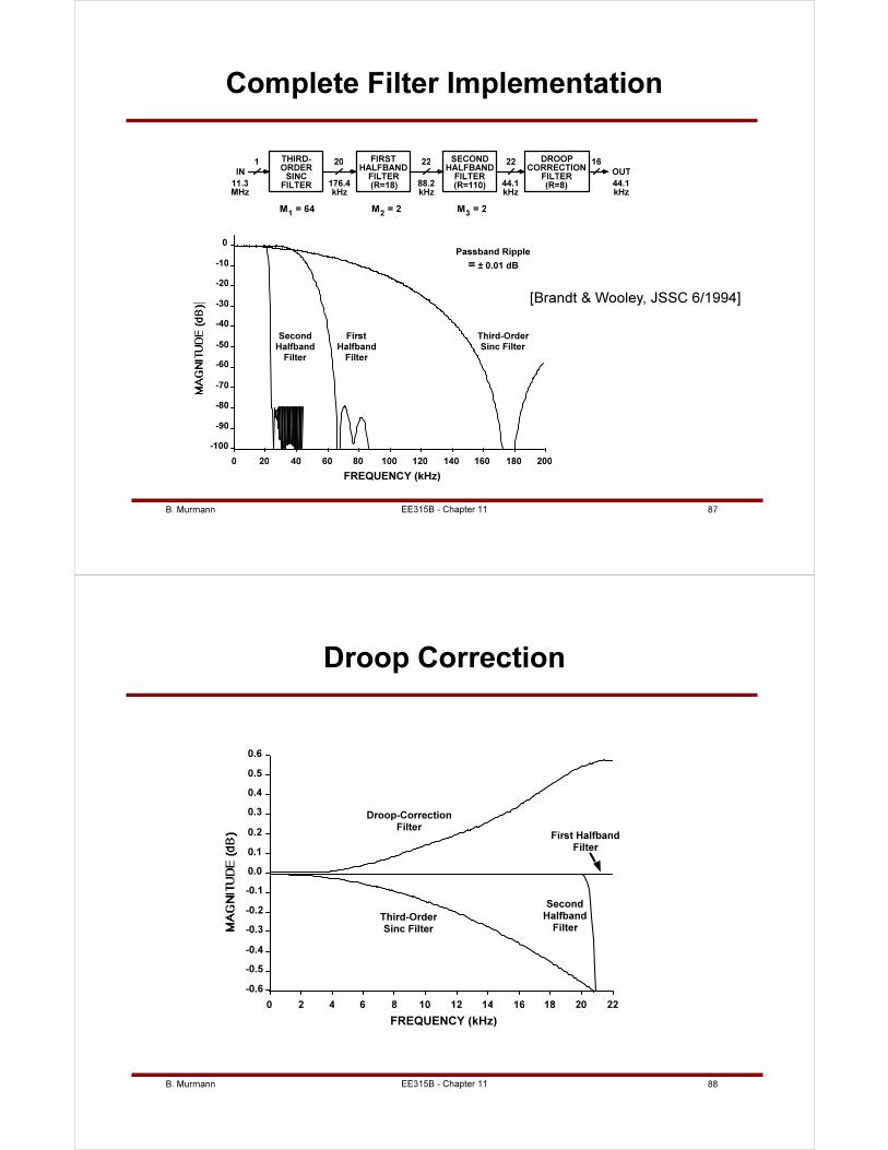
B. Murmann 87EE315B - Chapter 11
Complete Filter Implementation
THIRD- ORDER
SINC FILTER
FIRST HALFBAND
FILTER (R=18)
SECOND HALFBAND
FILTER (R=110)
DROOP CORRECTION
FILTER (R=8)176.4
kHz88.2 kHz
44.1 kHz
OUT
44.1 kHz
IN
11.3 MHz
M = 22
M = 641
M = 23
1 20 22 22 16
Third-Order
Sinc Filter
200180160140120100806040200
-100
-90
-80
-70
-60
-50
-40
-30
-20
-10
0
FREQUENCY (kHz)
First
Halfband
Filter
Second
Halfband
Filter
Passband Ripple
= ± 0.01 dB
[Brandt & Wooley, JSSC 6/1994]
B. Murmann 88EE315B - Chapter 11
Droop Correction
2220181614121086420
-0.6
-0.5
-0.4
-0.3
-0.2
-0.1
0.0
0.1
0.2
0.3
0.4
0.5
0.6
FREQUENCY (kHz)
First Halfband
Filter
Second
Halfband
Filter
Droop-Correction
Filter
Third-Order
Sinc Filter
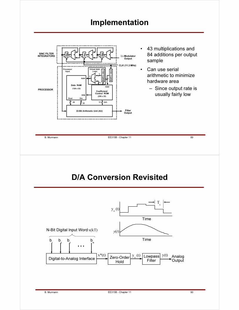
B. Murmann 89EE315B - Chapter 11
Implementation
• 43 multiplications and
84 additions per output
sample
• Can use serial
arithmetic to minimize
hardware area
– Since output rate is
usually fairly low
2020 2020 2020
Dout
Data RAM
22-Bit Arithmetic Unit (AU)
Coefficient/ Control ROM
7
7
CLK (11.3 MHz)
Addr
Addr
Ctrl.13
Din
Filter Output
(128 x 22)
22
(256 x 22)R/W
7
8
22
Σ∆ Modulator Output
PROCESSOR
SINC FILTER INTEGRATORS
Virtual Addr. Logic
Processor Input
B. Murmann 90EE315B - Chapter 11
D/A Conversion Revisited
LowpassFilter
N-Bit Digital lnput Word x(kT)
Digital-to-Analog InterfaceAnalog
b1
b2
b3
bN
• • •
Output
y(t)
yH(t)
Time
y(t)
Time
TS
Zero-OrderHold
x*(t) yH
(t)
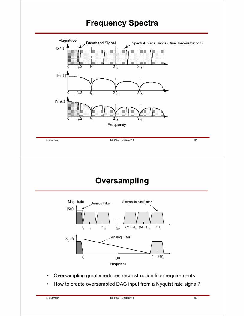
B. Murmann 91EE315B - Chapter 11
Frequency Spectra
Spectral Images
fS 2fSfS/20 3fS
fS 2fSfS/20 3fS
Frequency
fS 2fSfS/20 3fS
|YH(f)|
|PZ(f)|
|X*(f)|
Baseband SignalMagnitude
Spectral Image Bands (Dirac Reconstruction)
B. Murmann 92EE315B - Chapter 11
Oversampling
• Oversampling greatly reduces reconstruction filter requirements
• How to create oversampled DAC input from a Nyquist rate signal?
|X(f)|
Magnitude
Frequency
|XM
(f)|
M fN
(M-1) fN
(M-2) fN
2 fN
fN
fS = M f
N
…
Spectral Images
Analog Filter
Analog Filter
fB
fB
(a)
(b)
Spectral Image Bands
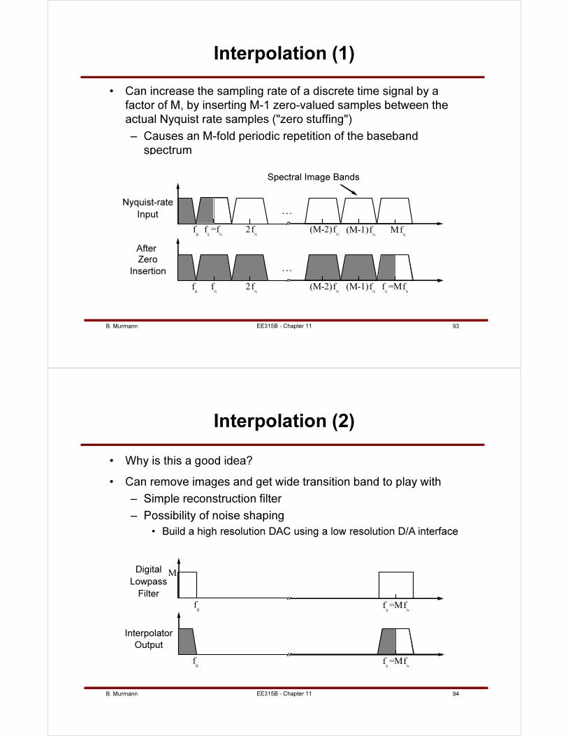
B. Murmann 93EE315B - Chapter 11
Interpolation (1)
• Can increase the sampling rate of a discrete time signal by a
factor of M, by inserting M-1 zero-valued samples between the
actual Nyquist rate samples ("zero stuffing")
– Causes an M-fold periodic repetition of the baseband
spectrum
Nyquist-rate
After
Input
Zero
…
Spectral Images
Insertion …
fS
=M fN
(M-1) fN
(M-2) fN
2 fN
fN
M fN
(M-1) fN
(M-2) fN
2 fN
fS
=fN
fB
fB
Spectral Image Bands
B. Murmann 94EE315B - Chapter 11
Interpolation (2)
Digital
Interpolator
Lowpass
Output
Filter
S NNNNN
M
fB
fB
B
fS
=M fN
fS
=M fN
• Why is this a good idea?
• Can remove images and get wide transition band to play with
– Simple reconstruction filter
– Possibility of noise shaping
• Build a high resolution DAC using a low resolution D/A interface
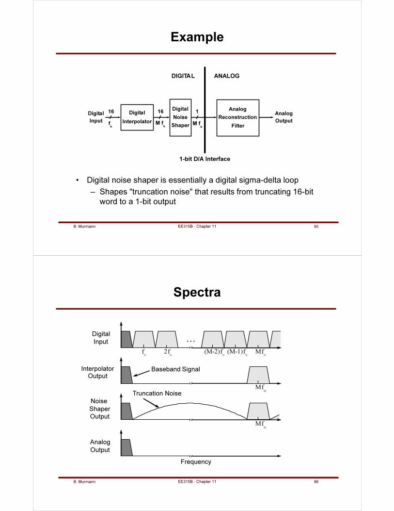
B. Murmann 95EE315B - Chapter 11
Example
• Digital noise shaper is essentially a digital sigma-delta loop
– Shapes "truncation noise" that results from truncating 16-bit
word to a 1-bit output
Digital
InputfN
16
M fN
M fN
Digital
Interpolator
Digital
Noise
Shaper
Reconstruction
Filter
Analog
ANALOGDIGITAL
1-bit D/A Interface
Analog
Output
16 1
B. Murmann 96EE315B - Chapter 11
Spectra
Digital
Interpolator
Noise
Analog
Input
Output
Shaper
Output
M fN
(M-1) fN
(M-2) fN
2 fN
fN
M fN
…
M fN
Output
Spectral Images
Quantization Noise
Baseband Signal
Frequency
Truncation Noise
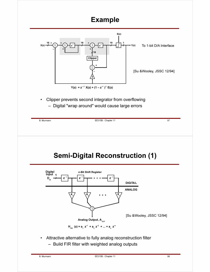
B. Murmann 97EE315B - Chapter 11
Example
• Clipper prevents second integrator from overflowing
– Digital "wrap around" would cause large errors
Y(z) = z – 2
X(z) + (1 – z –1
) 2
E(z)
Σ z–1X(z) Y(z)
+Σ
Σ
2
Σ z–1
+ +
116
E(z)
–
–
+
+
+
Clipper
18 19
18
To 1-bit D/A Interface
[Su &Wooley, JSSC 12/94]
B. Murmann 98EE315B - Chapter 11
Semi-Digital Reconstruction (1)
• Attractive alternative to fully analog reconstruction filter
– Build FIR filter with weighted analog outputs
z– 1
z– 1
a1
Σ
a2
an
DigitalInput
n -Bit Shift Register
Analog Output, AOUT
HFIR
(z) = a1 z
–1 + a
2 z
–2 + ... + a
n z
–n
DIGITAL
ANALOG
1D
IN
. . .
z– 1
. . .
[Su &Wooley, JSSC 12/94]
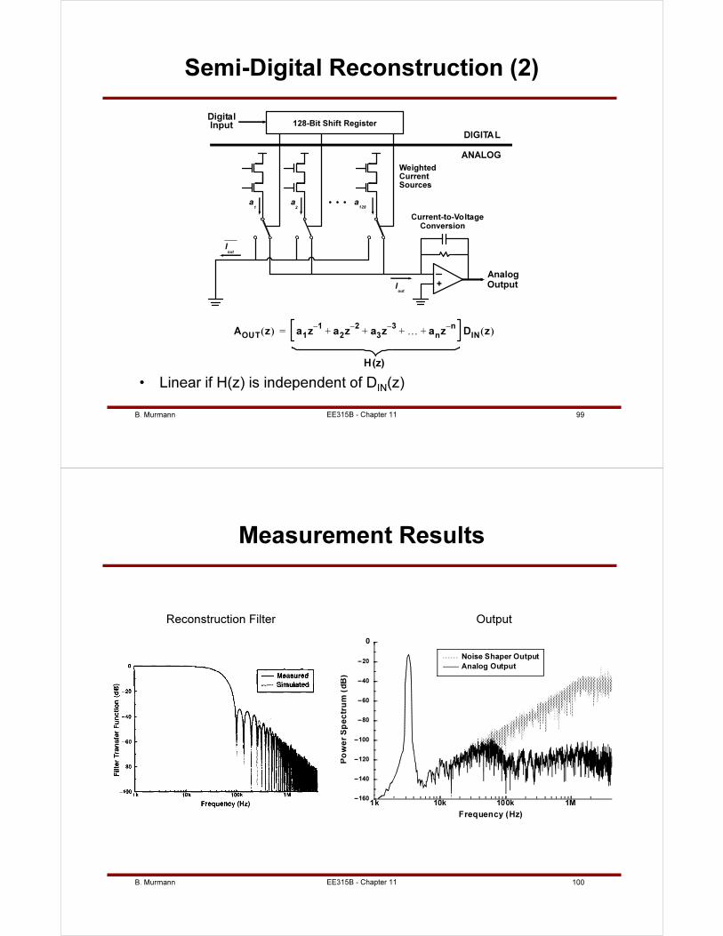
B. Murmann 99EE315B - Chapter 11
Semi-Digital Reconstruction (2)
• Linear if H(z) is independent of DIN
(z)
+AnalogOutput
DigitalInput 128-Bit Shift Register
a1
Current-to-VoltageConversion
WeightedCurrentSources
DIGITAL
ANALOG
Iout
Iout
a2
a128
. . .
AOUT
z( ) a1z
1–a
2z
2–a
3z
3–… a
nz
n –
+ + + + DIN
z( )=
H (z)
B. Murmann 100EE315B - Chapter 11
Measurement Results
1k 10k 100k 1M–160
–140
–120
–100
–80
–60
–40
–20
Frequency (Hz)
Po
we
r S
pe
ctr
um
(d
B)
Noise Shaper Output
Analog Output
0
Reconstruction Filter Output
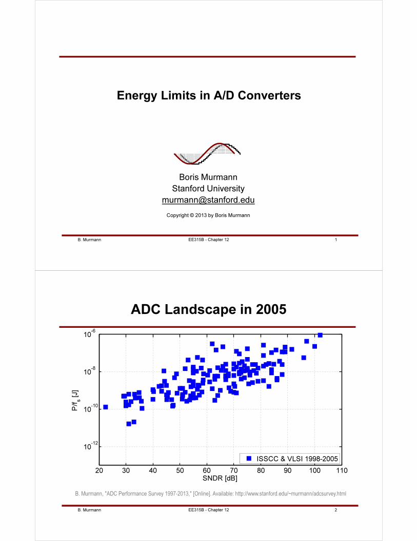
B. Murmann 1EE315B - Chapter 12
Energy Limits in A/D Converters
Boris Murmann
Stanford University
Copyright © 2013 by Boris Murmann
B. Murmann 2
ADC Landscape in 2005
B. Murmann, "ADC Performance Survey 1997-2013," [Online]. Available: http://www.stanford.edu/~murmann/adcsurvey.html
20 30 40 50 60 70 80 90 100 110
10-12
10-10
10-8
10-6
SNDR [dB]
P/fs [J]
ISSCC & VLSI 1998-2005
EE315B - Chapter 12
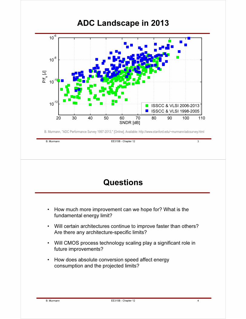
B. Murmann 3
ADC Landscape in 2013
B. Murmann, "ADC Performance Survey 1997-2013," [Online]. Available: http://www.stanford.edu/~murmann/adcsurvey.html
20 30 40 50 60 70 80 90 100 110
10-12
10-10
10-8
10-6
SNDR [dB]
P/fs [J]
ISSCC & VLSI 2006-2013
ISSCC & VLSI 1998-2005
EE315B - Chapter 12
B. Murmann 4
Questions
• How much more improvement can we hope for? What is the
fundamental energy limit?
• Will certain architectures continue to improve faster than others?
Are there any architecture-specific limits?
• Will CMOS process technology scaling play a significant role in
future improvements?
• How does absolute conversion speed affect energy
consumption and the projected limits?
EE315B - Chapter 12
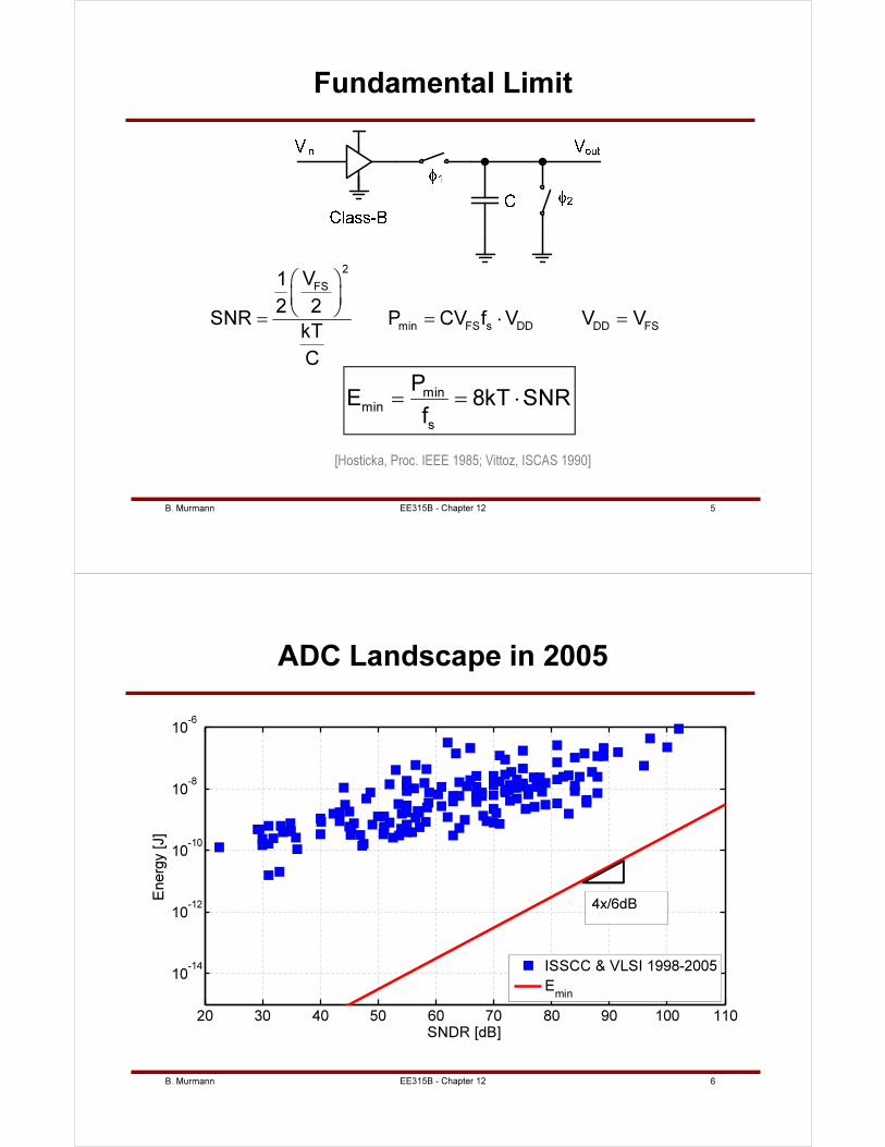
B. Murmann 5
Fundamental Limit
2
FSV1
2 2SNR
kT
C
=
min FS s DDP CV f V= ⋅
DD FSV V=
[Hosticka, Proc. IEEE 1985; Vittoz, ISCAS 1990]
min
min
s
PE 8kT SNR
f= = ⋅
EE315B - Chapter 12
B. Murmann 6
20 30 40 50 60 70 80 90 100 110
10-14
10-12
10-10
10-8
10-6
SNDR [dB]
Energ
y [J]
ISSCC & VLSI 1998-2005
Emin
ADC Landscape in 2005
4x/6dB
EE315B - Chapter 12
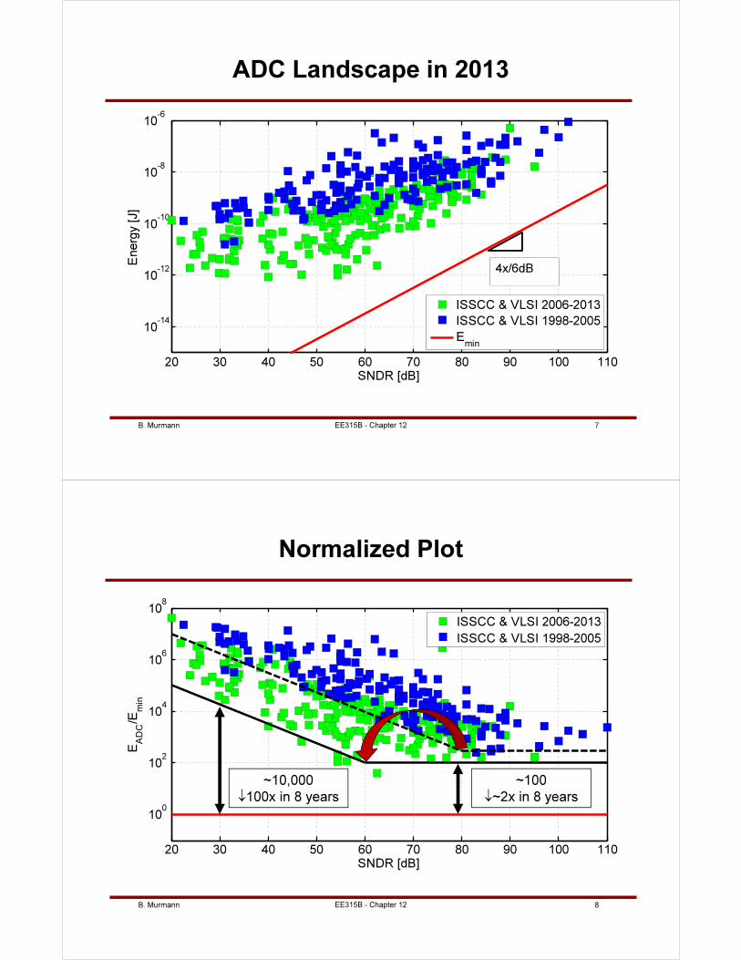
B. Murmann 7
20 30 40 50 60 70 80 90 100 110
10-14
10-12
10-10
10-8
10-6
SNDR [dB]
Energ
y [J]
ISSCC & VLSI 2006-2013
ISSCC & VLSI 1998-2005
Emin
ADC Landscape in 2013
4x/6dB
EE315B - Chapter 12
B. Murmann 8
20 30 40 50 60 70 80 90 100 110
100
102
104
106
108
SNDR [dB]
EADC/E
min
ISSCC & VLSI 2006-2013
ISSCC & VLSI 1998-2005
Normalized Plot
~10,000
↓100x in 8 years
~100
↓~2x in 8 years
EE315B - Chapter 12
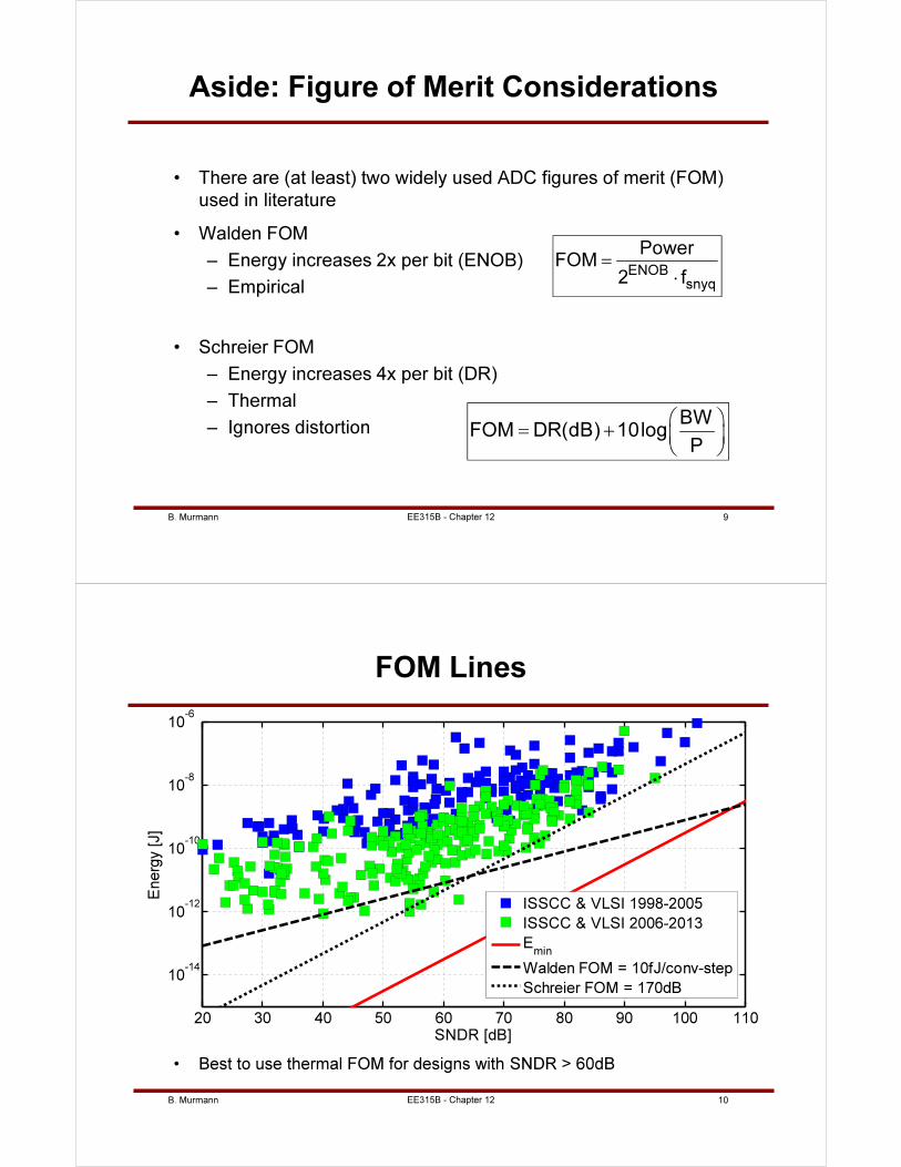
B. Murmann 9
Aside: Figure of Merit Considerations
• There are (at least) two widely used ADC figures of merit (FOM)
used in literature
• Walden FOM
– Energy increases 2x per bit (ENOB)
– Empirical
• Schreier FOM
– Energy increases 4x per bit (DR)
– Thermal
– Ignores distortion
ENOBsnyq
PowerFOM
2 f=
⋅
BWFOM DR(dB) 10log
P
= +
EE315B - Chapter 12
B. Murmann 10
FOM Lines
• Best to use thermal FOM for designs with SNDR > 60dB
20 30 40 50 60 70 80 90 100 110
10-14
10-12
10-10
10-8
10-6
SNDR [dB]
Energ
y [J]
ISSCC & VLSI 1998-2005
ISSCC & VLSI 2006-2013
Emin
Walden FOM = 10fJ/conv-step
Schreier FOM = 170dB
EE315B - Chapter 12
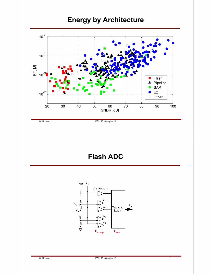
B. Murmann 11
Energy by Architecture
EE315B - Chapter 12
20 30 40 50 60 70 80 90 100
10-12
10-10
10-8
10-6
SNDR [dB]
P/fs [J]
Flash
Pipeline
SAR
∆Σ
Other
B. Murmann 12
Flash ADC
EencEcomp
EE315B - Chapter 12
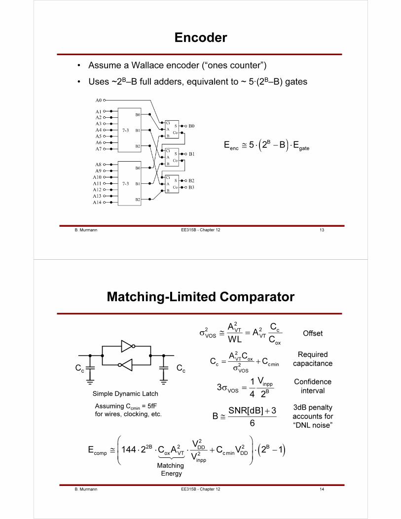
B. Murmann 13
Encoder
• Assume a Wallace encoder (“ones counter”)
• Uses ~2B–B full adders, equivalent to ~ 5∙(2B–B) gates
( )B
enc gateE 5 2 B E≅ ⋅ − ⋅
EE315B - Chapter 12
B. Murmann 14
Matching-Limited Comparator
Simple Dynamic Latch
2
2 2 cVT
VOS VT
ox
CAA
WL Cσ ≅ =
2
VT ox
c cmin2
VOS
A CC C= +
σ
( )2
2B 2 2 BDDcomp ox VT cmin DD2
inpp
VE 144 2 C A C V 2 1
V
≅ ⋅ ⋅ ⋅ + ⋅ −
14243
SNR[dB] 3B
6
+≅
CcCc
Assuming Ccmin = 5fF
for wires, clocking, etc.
inpp
VOS B
V13
4 2σ =
Matching
Energy
3dB penalty
accounts for
“DNL noise”
Offset
Required
capacitance
Confidence
interval
EE315B - Chapter 12
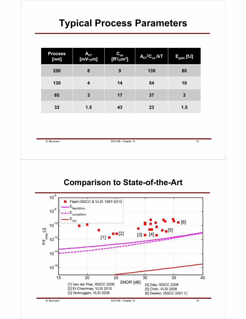
B. Murmann 15
Typical Process Parameters
Process
[nm]
AVT
[mV-µm]
Cox
[fF/µm2]AVT
2Cox /kT Egate [fJ]
250 8 9 139 80
130 4 14 54 10
65 3 17 37 3
32 1.5 43 23 1.5
EE315B - Chapter 12
B. Murmann 16
15 20 25 30 35 40
10-16
10-14
10-12
10-10
10-8
10-6
SNDR [dB]
P/fsnyq [J]
Flash ISSCC & VLSI 1997-2012
Eflash65nm
Ecomp65nm
Emin
Comparison to State-of-the-Art
[4] Daly, ISSCC 2008
[5] Chen, VLSI 2008
[6] Geelen, ISSCC 2001 (!)
[6]
[1]
[5]
[1] Van der Plas, ISSCC 2006
[2] El-Chammas, VLSI 2010
[3] Verbruggen, VLSI 2008
[3] [4][2]
EE315B - Chapter 12
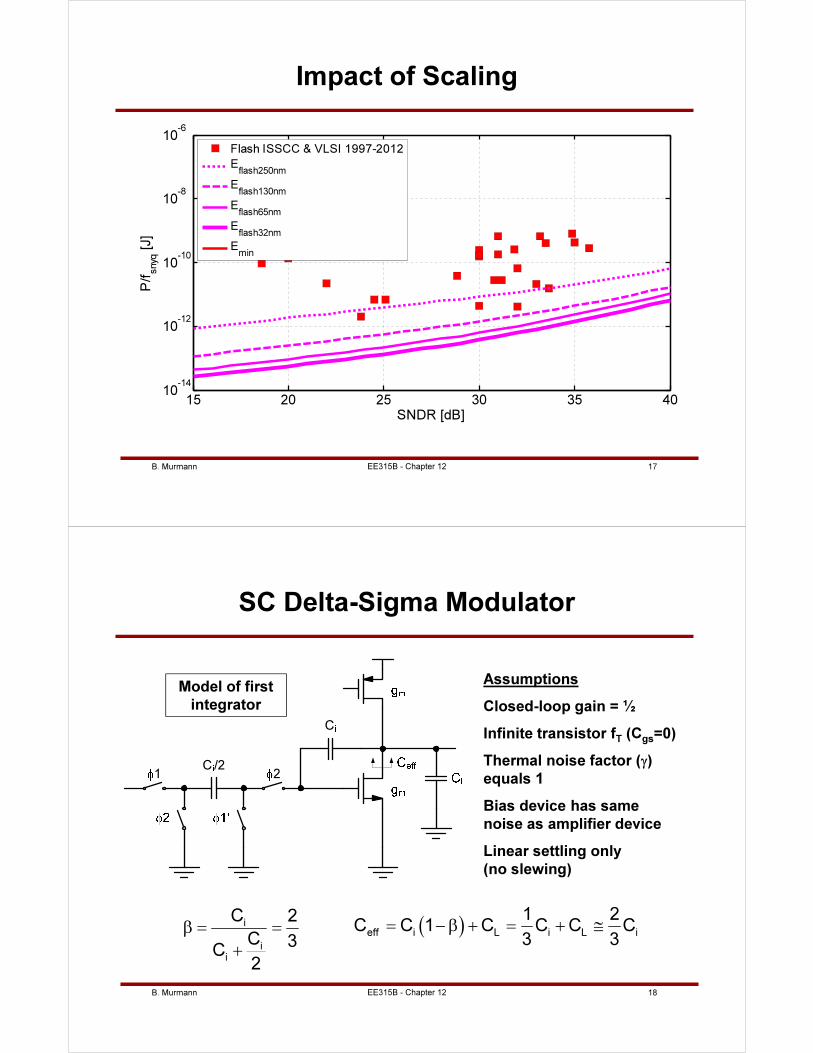
B. Murmann 17
Impact of Scaling
15 20 25 30 35 4010
-14
10-12
10-10
10-8
10-6
SNDR [dB]
P/fsnyq [J]
Flash ISSCC & VLSI 1997-2012
Eflash250nm
Eflash130nm
Eflash65nm
Eflash32nm
Emin
EE315B - Chapter 12
B. Murmann 18
SC Delta-Sigma Modulator
Assumptions
Closed-loop gain = ½
Infinite transistor fT (Cgs=0)
Thermal noise factor (γ)
equals 1
Bias device has same
noise as amplifier device
Linear settling only
(no slewing)
i
i
i
C 2
C 3C
2
β = =
+
( )eff i L i L i
1 2C C 1 C C C C
3 3= −β + = + ≅
1C /2
C
2
Model of first
integrator
EE315B - Chapter 12

B. Murmann 19
SC Integrator Constraints
2
inpp
eff
V1
2 2SNR
kT 14C OSR
≅
Thermal noise
sets Ceff
( )eff s s
m
d
C T / 2 T / 2
g 1 ln SNRln
τ = = ≅β
ε
Settling time
sets gm
gm
sets powerm
DD
m
D
gP V
g
I
=
EE315B - Chapter 12
B. Murmann 20
Pulling It All Together
Excess noise
Finite β
( )
2
DDintDT
minpp DD
D
V 1 1E 64 kT SNR ln SNR
gV V
I
= ⋅ ⋅ ⋅ ⋅ ⋅ ⋅
64748
14243
Settling
“Number of τ”
Supply
utilization
VDD
penalty
Transconductor
efficiency
• For settling with ~10 time constants and VDD=1V,
gm/ID=1/(1.5kT/q), Vinpp=0.5V, we have
E ≅ 200kT · SNR
EE315B - Chapter 12
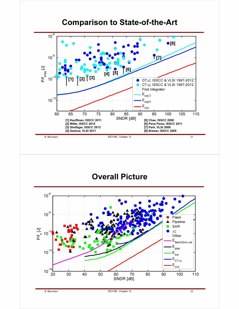
B. Murmann 21
60 65 70 75 80 85 90 95 100 105 110
10-12
10-10
10-8
10-6
SNDR [dB]
P/fsnyq [J]
DT∆Σ ISSCC & VLSI 1997-2012
CT∆Σ ISSCC & VLSI 1997-2012
First Integrator
EintCT
EintDT
Emin
Comparison to State-of-the-Art
[6]
[5] Chae, ISSCC 2008
[6] Pena Perez, ISSCC 2011
[7] Park, VLSI 2008
[8] Brewer, ISSCC 2005
[3]
[7]
[1] [2]
[1] Kauffman, ISSCC 2011
[2] Witte, ISSCC 2012
[3] Shettigar, ISSCC 2012
[4] Gealow, VLSI 2011
[5]
[8]
[4]
EE315B - Chapter 12
B. Murmann 22
Overall Picture
EE315B - Chapter 12
20 30 40 50 60 70 80 90 100 11010
-14
10-12
10-10
10-8
10-6
SNDR [dB]
P/fs [J]
Flash
Pipeline
SAR
∆Σ
Other
Eflash32nm,cal
Epipe
Esar
ECT∆Σ
Emin
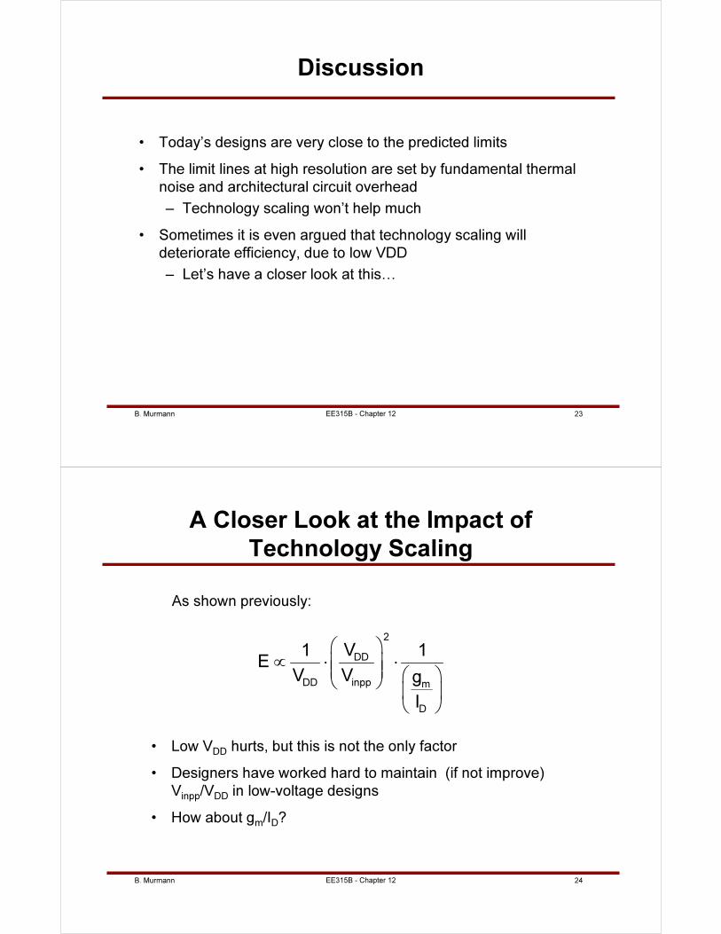
B. Murmann 23
Discussion
• Today’s designs are very close to the predicted limits
• The limit lines at high resolution are set by fundamental thermal
noise and architectural circuit overhead
– Technology scaling won’t help much
• Sometimes it is even argued that technology scaling will
deteriorate efficiency, due to low VDD
– Let’s have a closer look at this…
EE315B - Chapter 12
B. Murmann 24
A Closer Look at the Impact of
Technology Scaling
• Low VDD hurts, but this is not the only factor
• Designers have worked hard to maintain (if not improve)
Vinpp/VDD in low-voltage designs
• How about gm/ID?
2
DD
DD inpp m
D
V1 1E
V V g
I
∝ ⋅ ⋅
As shown previously:
EE315B - Chapter 12
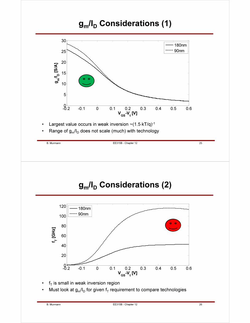
B. Murmann 25
-0.2 -0.1 0 0.1 0.2 0.3 0.4 0.5 0.60
5
10
15
20
25
30
VGS
-Vt [V]
gm
/ID [
S/A
]
180nm
90nm
gm
/ID
Considerations (1)
• Largest value occurs in weak inversion ~(1.5⋅kT/q)-1
• Range of gm/ID does not scale (much) with technology
EE315B - Chapter 12
B. Murmann 26
-0.2 -0.1 0 0.1 0.2 0.3 0.4 0.5 0.60
20
40
60
80
100
120
VGS
-Vt [V]
f T [
GH
z]
180nm
90nm
gm
/ID
Considerations (2)
• fT is small in weak inversion region
• Must look at gm/ID for given fT requirement to compare technologies
EE315B - Chapter 12
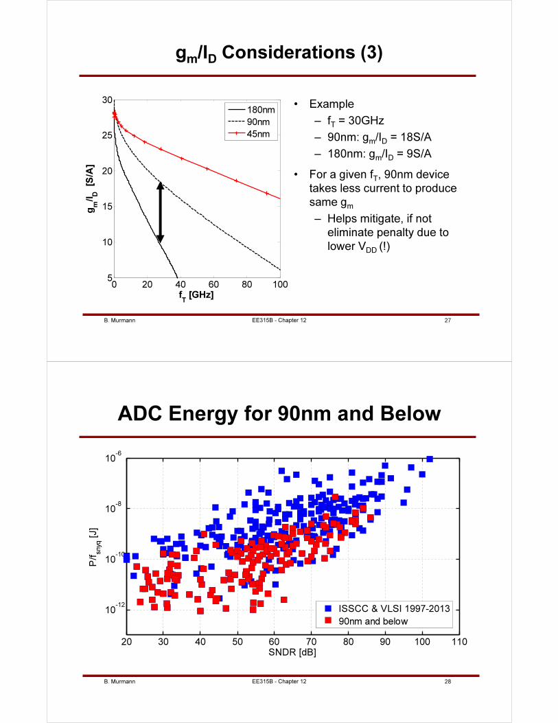
B. Murmann 27
0 20 40 60 80 1005
10
15
20
25
30
gm
/ID [S
/A]
fT [GHz]
180nm
90nm
45nm
gm
/ID
Considerations (3)
• Example
– fT = 30GHz
– 90nm: gm/ID = 18S/A
– 180nm: gm/ID = 9S/A
• For a given fT, 90nm device
takes less current to produce
same gm
– Helps mitigate, if not
eliminate penalty due to
lower VDD (!)
EE315B - Chapter 12
B. Murmann 28
ADC Energy for 90nm and Below
EE315B - Chapter 12
20 30 40 50 60 70 80 90 100 110
10-12
10-10
10-8
10-6
SNDR [dB]
P/fsnyq [J]
ISSCC & VLSI 1997-2013
90nm and below
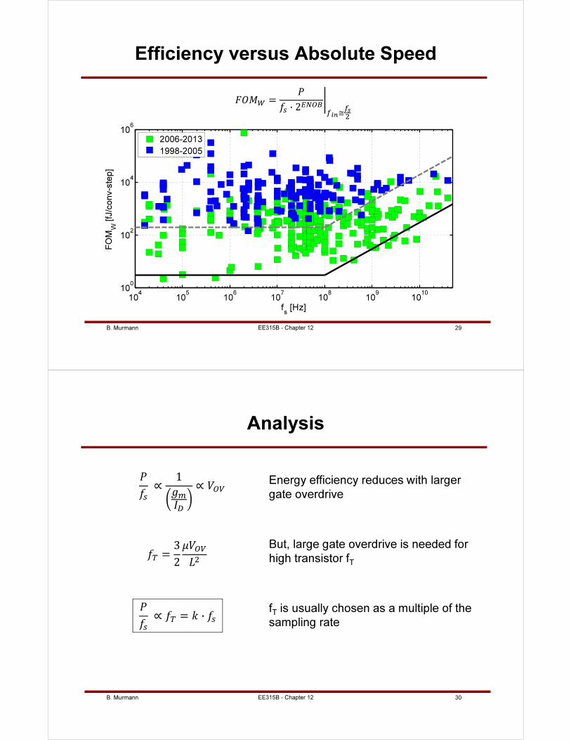
B. Murmann 29
104
105
106
107
108
109
1010
100
102
104
106
fs [Hz]
FO
MW
[fJ
/conv-s
tep]
2006-2013
1998-2005
Efficiency versus Absolute Speed
=
· 2≅
EE315B - Chapter 12
B. Murmann 30
Analysis
∝
1
∝
=3
2
∝ = ·
Energy efficiency reduces with larger
gate overdrive
But, large gate overdrive is needed for
high transistor fT
fT is usually chosen as a multiple of the
sampling rate
EE315B - Chapter 12
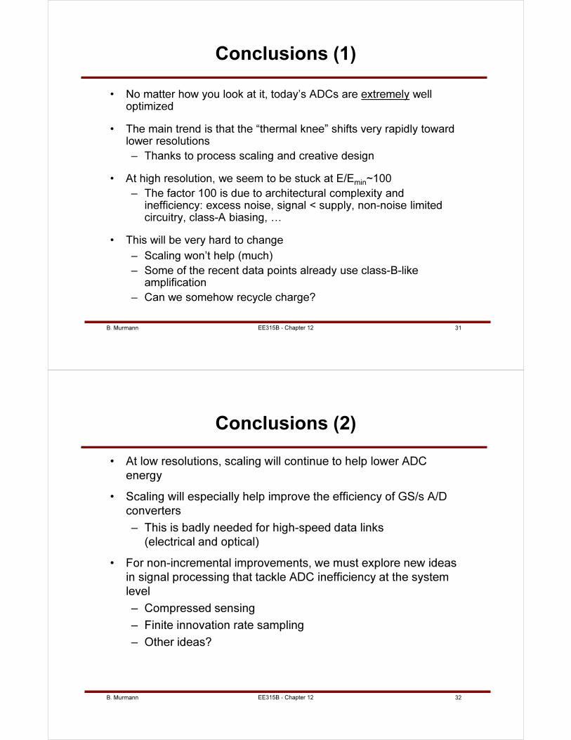
B. Murmann 31
Conclusions (1)
• No matter how you look at it, today’s ADCs are extremely well optimized
• The main trend is that the “thermal knee” shifts very rapidly toward lower resolutions
– Thanks to process scaling and creative design
• At high resolution, we seem to be stuck at E/Emin
~100
– The factor 100 is due to architectural complexity and inefficiency: excess noise, signal < supply, non-noise limited circuitry, class-A biasing, …
• This will be very hard to change
– Scaling won’t help (much)
– Some of the recent data points already use class-B-like amplification
– Can we somehow recycle charge?
EE315B - Chapter 12
B. Murmann 32
Conclusions (2)
• At low resolutions, scaling will continue to help lower ADC
energy
• Scaling will especially help improve the efficiency of GS/s A/D
converters
– This is badly needed for high-speed data links
(electrical and optical)
• For non-incremental improvements, we must explore new ideas
in signal processing that tackle ADC inefficiency at the system
level
– Compressed sensing
– Finite innovation rate sampling
– Other ideas?
EE315B - Chapter 12
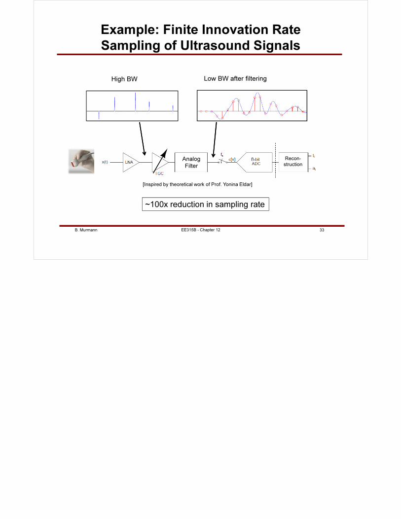
B. Murmann 33
Example: Finite Innovation Rate
Sampling of Ultrasound Signals
Analog
Filter
Recon-
struction
High BW Low BW after filtering
~100x reduction in sampling rate
[Inspired by theoretical work of Prof. Yonina Eldar]
EE315B - Chapter 12


