Embed Size (px)
Citation preview
Received January 29, 2020, accepted February 11, 2020, date of publication February 17, 2020, date of current version February 27, 2020.
Digital Object Identifier 10.1109/ACCESS.2020.2974552
Wideband Bandpass Filters Using aNovel Thick Metallization TechnologyCELIA GOMEZ-MOLINA 1, ALEJANDRO PONS-ABENZA1, (Student Member, IEEE),JAMES DO 2, FERNANDO QUESADA-PEREIRA 1, (Member, IEEE),XIAOGUANG LIU 2, (Senior Member, IEEE),JUAN SEBASTIAN GOMEZ-DIAZ 2, (Senior Member, IEEE),AND ALEJANDRO ALVAREZ-MELCON 1, (Senior Member, IEEE)1Department of Information Technologies and Communications, Universidad Politécnica de Cartagena, 30202 Cartagena, Spain2Department of Electrical and Computer Engineering, University of California at Davis, Davis, CA 95616, USA
Corresponding author: Celia Gomez-Molina ([email protected])
This work was supported in part by the National Science Foundation with CAREER under Grant ECCS-1749177, in part by the SpanishGovernment, Ministerio de Educación, Cultura y Deporte under Grant FPU15/02883, and in part by the Ministerio de Economía yCompetitividad through the Coordinated Project under Grant TEC2016-75934-C4-R and Grant PRX18/00092.
ABSTRACT A new class of wideband bandpass filters based on using thick metallic bars as microwaveresonators is presented in this work. These bars provide a series of advantages over fully planar printedtechnologies, including higher coupling levels between resonators, higher unloaded quality factors QU ,and larger bandwidths implemented with compact structures. In comparison to dielectric and waveguideresonators filters, higher bandwidths together with lower weight and footprint reduction are achieved withthe proposed thick bars technology. Moreover, thick bar resonators can easily be coupled to an additionalresonance excited in a box used for shielding, allowing to realize transversal topologies able to implementtransmission zeros at desired frequencies. To illustrate the capabilities of this technology, three microwavefilters with different topologies have been designed. One of the designed filters has been manufactured andtested using copper bars inside an aluminum housing partially filledwith Teflon.Measured data demonstratesa fractional bandwidth of FBW = 32%, spurious free range SFR > 50%, unloaded quality factor ofQU = 1180, insertion losses over 0.16 dB and return losses over 20 dB, without requiring any post-tuningoperation on the prototype. This result confirms the exciting performance of the proposed technology forwideband applications.
INDEX TERMS Hybrid waveguide microstrip technology, microwave filters, resonator filters, transmissionzeros, transversal filters, wideband filters.
I. INTRODUCTIONWideband filters are required in modern communication sys-tems, including wireless communications, 5G, satellites, orin artificial intelligence platforms. Most of these applicationsrequire compact solutions for filters, with good performancein terms of insertion losses (IL), return losses (RL) andunloaded quality factors (QU ).In applications where the footprint and volume are critical,
planar technologies, such as microstrip [1], [2], stripline [3]or coplanar [4], [5] are usually employed. Using these tech-nologies, the level of losses is normally sacrificed in order toproduce structures with reduced dimensions and low weight.
The associate editor coordinating the review of this manuscript and
approving it for publication was Yingsong Li .
Among the planar solutions, microstrip technology [1] isone of the most employed in practice, due to the compactnessachieved, ease of integration and low-cost fabrication. Unfor-tunately, the most important limitations faced by microstripresonator filters [2] for these applications are normally smallbandwidths and low QU . Some previous works have tried toimplement broadband filters using microstrip line resonators.For instance, in [6], the authors use concentric open-loop res-onators to reduce the size of the filter and achieve a fractionalbandwidth FBW ≈ 10%. It is challenging to enhance thebandwidth of these microwave filters beyond these limits,mainly because very strong couplings are required betweenresonators and in the input/output (I/O) ports. However, thecoupling levels achievable with microstrip line resonators arelow, which limit in practice the implementation of wideband
34962 This work is licensed under a Creative Commons Attribution 4.0 License. For more information, see http://creativecommons.org/licenses/by/4.0/ VOLUME 8, 2020
C. Gomez-Molina et al.: Wideband Bandpass Filters Using a Novel Thick Metallization Technology
responses. The second limiting factor of printed microstriptechnology is the relatively low QU . This factor is typicallyless than 150 for this technology. The low QU is mainly dueto the field distribution of the microstrip mode, and the verysmall thickness of printed resonators.
Alternative hybrid technologies are the substrate integratedwaveguide (SIW) [7], [8], Empty SIW (ESIW) [9], QuarterMode SIW (QMSIW) [10] or Air Filled SIW (ASIW) [11].Using this family of substrate integrate technology, the QUis increased with respect to microstrip technology while thereduced dimensions are still maintained. Thus, this technol-ogy represents a good trade-off between volume and QU .For instance, in [8], the achievable QU is around 640 for aFBW = 16.5%. The main disadvantage of this technology isthe transition to other planar technologies. In SIW filters, lossperformance is also sacrificed at the expense of compactness.
In applications where higherQU and robustness are strictlyrequired, other non-planar alternatives, such as dielectric res-onators [12], [13] or waveguide technology [14], [15] can beused. However, the compactness and low-cost manufacturingfeatures of planar technologies are compromised.
In [12], the authors proposed the use of high dielectricconstant strip resonators deposited on a low permittivitysubstrate. Using these dielectric resonators, filters withQU ≈ 880 were demonstrated. As observed, the achievedQU using this technology is higher as compared to the tra-ditional microstrip or SIW technologies (see [12]). However,in that work a standard tapped feeding line was employed toimplement the I/O couplings. Due to this arrangement, ratherlow I/O coupling values could be implemented [12], resultinginto a fractional bandwidth of only FBW = 3.3%. HigherQU can be achieved using dielectric resonators in waveguidetechnology as in [13]. In [13], the fractional bandwidth is alsoFBW ≈ 3% but with a higher quality factor of QU ≈ 1750.However, the footprint is increased in comparison to thesolution in [12].
Instead, using directlywaveguide resonators the achievablefractional bandwidths can be increased as compared to theprevious technologies (typically less than 20%), as it wasfor instance reported in [14]. However, much higher QUare possible in waveguide technology. For instance, in [15]measurements demonstrate an unloaded quality factor aroundQU = 2700 and a fractional bandwidth of FBW = 8.3%.Even though compact solutions have been proposed [15],the sizes of waveguide filters are normally higher than withother implementations using planar or hybrid technologies.
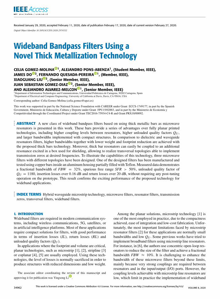
In this context, we present in this work an alternativetechnology to realize wideband filters with reduced footprintsin comparison to waveguide and dielectric resonator tech-nologies, while maintaining large QU as compared to planartechnologies. A 3D view of the proposed technology is shownin Fig. 1.
The proposed technology employs thick half-wavelengthmetallic bars buried in a dielectric medium. A metallic enclo-sure is employed to avoid spurious radiation (see Fig. 1).In comparison to planar technologies, we will demonstrate
FIGURE 1. 3D view of the proposed filter technology based on bulky barsburied in a dielectric medium. The sketch shows an example of a filterusing three bar resonators enclosed in a house cavity. I/O couplings areimplemented with the step impedance discontinuity produced from adirect connection of the coaxial connectors with the first/last barresonators.
that the thick bars significantly increase the achievable cou-pling levels among resonators, while providing larger QU .The use of metallic bars with large thickness also produces astrong decrease in the characteristic impedance of the guidedTEM mode. Consequently, we demonstrate that I/O couplingscan be implemented by introducing a step impedance dis-continuity between the coaxial connectors and the first/lastresonators. In this way, explicit I/O feeding lines are avoided.The adjustment of this step impedance discontinuity togetherwith the capability to implement very large inter-resonatorcouplings, will enable to implement wideband frequencyresponses. Since no I/O lines are required, the footprint of thestructure is reduced as compared to standard boxedmicrostripprinted technology and SIW. However, the manufacturingcomplexity and volume are increased with respect to thesestrictly planar technologies.
In comparison to non-planar technologies, thick bar res-onators exhibit QU s that are similar than the ones obtainedusing dielectric resonators, but lower than waveguide res-onators. However, the I/O mechanism proposed in this papertogether with the high inter-resonator couplings achievablewith the thick bars allow to increase the achievable fractionalbandwidths. Themanufacturing complexity is similar to thesenon-planar technologies, while the weight, footprint and vol-ume are significantly reduced.
In this paper we also show that an additional resonant modecan be excited in the shielding cavity partially filled withdielectric, similar to the idea proposed in [16], [17]. In thoseworks, the I/O feeding lines were used to excite an additionalcavity box resonance. In this new structure, some of the barresonators, when adequately placed inside the cavity, can con-veniently couple to this additional resonant mode. This willallow for the implementation of transversal topologies [18],which can be used to produce transmission zeros at finitefrequencies in the insertion loss response of the filter.
VOLUME 8, 2020 34963
C. Gomez-Molina et al.: Wideband Bandpass Filters Using a Novel Thick Metallization Technology
To demonstrate these features, three filters are designedusing the proposed concept. First, a third order in-line filter isdesigned using only three thick bar resonators (not using thecavity mode). The filter is designed at C-band, with centerfrequency fc1 = 4.26 GHz, and bandwidth BW1 = 800 MHz,leading to fractional bandwidth of FBW1 = 18.78%. Then,a transversal-based topology of order four is implementedwith three bar resonators and one box resonator. The transver-sal filters are also designed at C-band, with center frequenciesfc2 = 3.26 GHz and fc3 = 3.35 GHz, and bandwidthsBW2 = 1.15 GHz and BW3 = 1.575 GHz, leading tofractional bandwidths of FBW2 = 35.28% and FBW3 =
47.01%, respectively.To validate the new concept, the first transversal filter
with lower bandwidth (BW2) has been manufactured usingthick bars made of copper, and Teflon as the dielectricmaterial. The external housing is made from aluminum.Measurements obtained from the manufactured hardwareshow very good agreement against initial target specifica-tions, and with respect to full-wave simulations obtained withAnsys High-Frequency Structure Simulator (HFSS) [19].The results demonstrate that the technology proposed inthis contribution represents a good trade-off between highperformance (in terms of IL, RL and QU ) and compactness,allowing the implementation of verywideband responses, andwith good spurious free range (SFR) performance.
II. THICK BAR TECHNOLOGY CHARACTERIZATIONIn this section, we first characterize the proposed tech-nology in terms of the resonators QU (subsection II-A),inter-resonator couplings (subsection II-B) and input/outputcouplings (subsection II-C). Special attention will be given tothe effect of the metallization thickness in these parameters,since this is the distinct feature as related to standard planartechnologies.
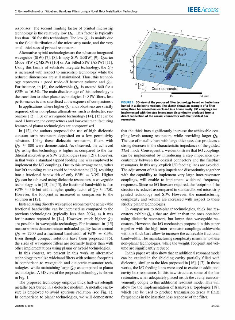
A. QUALITY FACTOR OF RESONATORSThe proposed technology is first characterized in terms ofachievable QU , by using one isolated metallic bulky baracting as a microwave resonator (see inset of Fig. 2). Thebehavior of the resonator according to its length (lr ) andwidth(wr2, see Fig. 1) is similar to a microstrip resonator. However,in contrast to printed microstrip resonators, the proposedtechnology uses bars with a non negligible thickness (lth, seeFig. 1). Due to this reason, in Fig. 2 we plot the value of QUfor different thickness of the resonator lth (0.1 mm < lth <5mm). The bar resonator is made of copper with conductivityσc = 5.8 ·107 S/m, and it is placed above a dielectric mediummade of Teflon (εr = 2.1, tan δ = 0.001) with thicknessld = 10 mm. All the elements are placed inside a cavity madeof aluminum with conductivity σb = 3.8 · 107 S/m.According to Fig. 2, results show a strong dependence of
QU with the resonator thickness lth. Maximum QU of 1360is obtained for the largest thickness lth = 5 mm. This valuedrops to QU = 830 for the thinnest considered metalizationof lth = 0.1 mm. This study, therefore, shows the first benefit
FIGURE 2. Unloaded quality factor (QU ) of a single bulky bar resonator,as a function of the thickness (lth). The geometry under test is shown inthe inset. The dielectric is Teflon with a relative permittivity of εr = 2.1and a loss tangent tan δ = 0.001. The bar is made using copper withconductivity σc = 5.8 · 107 S/m, and the box is made of aluminum withconductivity σb = 3.8 · 107 S/m. Other dimensions are ld = 10 mm,la = 10 mm, lr = 15 mm, wr = 2 mm (bar resonator width in the y axis),a = 30 mm and b = 20 mm (box dimension in the y axis). The testfrequency is fc = 5.56 GHz.
of the proposed technology, namely, the possibility of havingsignificantly larger QU values as compared to those obtainedusing printed resonators. This large QU can be attributed tothe extended metallic surface provided by the bulky bars,through which the induced currents can flow.
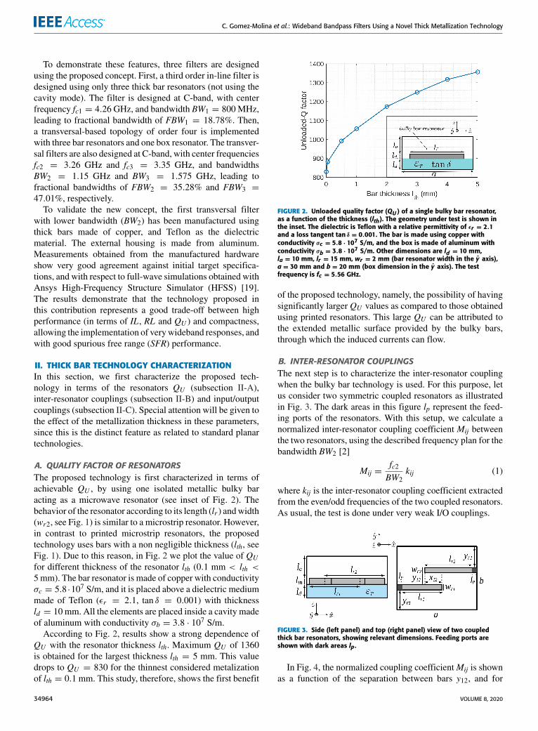
B. INTER-RESONATOR COUPLINGSThe next step is to characterize the inter-resonator couplingwhen the bulky bar technology is used. For this purpose, letus consider two symmetric coupled resonators as illustratedin Fig. 3. The dark areas in this figure lp represent the feed-ing ports of the resonators. With this setup, we calculate anormalized inter-resonator coupling coefficient Mij betweenthe two resonators, using the described frequency plan for thebandwidth BW2 [2]
Mij =fc2BW2
kij (1)
where kij is the inter-resonator coupling coefficient extractedfrom the even/odd frequencies of the two coupled resonators.As usual, the test is done under very weak I/O couplings.
FIGURE 3. Side (left panel) and top (right panel) view of two coupledthick bar resonators, showing relevant dimensions. Feeding ports areshown with dark areas lp.
In Fig. 4, the normalized coupling coefficientMij is shownas a function of the separation between bars y12, and for
34964 VOLUME 8, 2020
C. Gomez-Molina et al.: Wideband Bandpass Filters Using a Novel Thick Metallization Technology
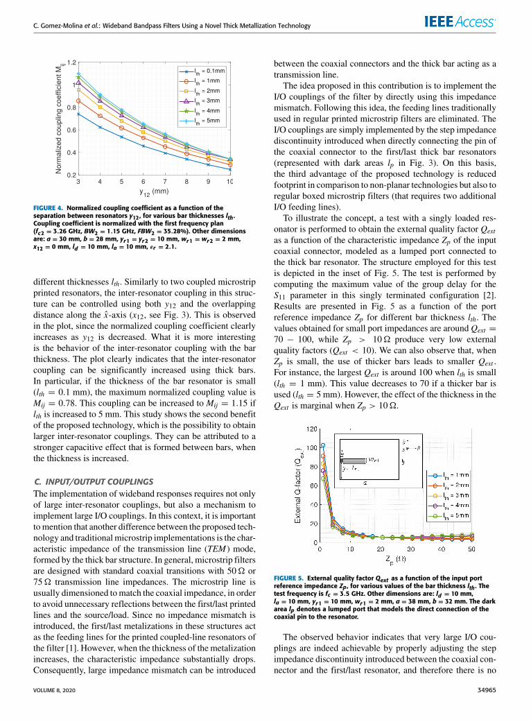
FIGURE 4. Normalized coupling coefficient as a function of theseparation between resonators y12, for various bar thicknesses lth.Coupling coefficient is normalized with the first frequency plan(fc2 = 3.26 GHz, BW2 = 1.15 GHz, FBW2 = 35.28%). Other dimensionsare: a = 30 mm, b = 28 mm, yr1 = yr2 = 10 mm, wr1 = wr2 = 2 mm,x12 = 0 mm, ld = 10 mm, la = 10 mm, εr = 2.1.
different thicknesses lth. Similarly to two coupled microstripprinted resonators, the inter-resonator coupling in this struc-ture can be controlled using both y12 and the overlappingdistance along the x-axis (x12, see Fig. 3). This is observedin the plot, since the normalized coupling coefficient clearlyincreases as y12 is decreased. What it is more interestingis the behavior of the inter-resonator coupling with the barthickness. The plot clearly indicates that the inter-resonatorcoupling can be significantly increased using thick bars.In particular, if the thickness of the bar resonator is small(lth = 0.1 mm), the maximum normalized coupling value isMij = 0.78. This coupling can be increased to Mij = 1.15 iflth is increased to 5 mm. This study shows the second benefitof the proposed technology, which is the possibility to obtainlarger inter-resonator couplings. They can be attributed to astronger capacitive effect that is formed between bars, whenthe thickness is increased.
C. INPUT/OUTPUT COUPLINGSThe implementation of wideband responses requires not onlyof large inter-resonator couplings, but also a mechanism toimplement large I/O couplings. In this context, it is importanttomention that another difference between the proposed tech-nology and traditionalmicrostrip implementations is the char-acteristic impedance of the transmission line (TEM ) mode,formed by the thick bar structure. In general, microstrip filtersare designed with standard coaxial transitions with 50� or75� transmission line impedances. The microstrip line isusually dimensioned tomatch the coaxial impedance, in orderto avoid unnecessary reflections between the first/last printedlines and the source/load. Since no impedance mismatch isintroduced, the first/last metalizations in these structures actas the feeding lines for the printed coupled-line resonators ofthe filter [1]. However, when the thickness of the metalizationincreases, the characteristic impedance substantially drops.Consequently, large impedance mismatch can be introduced
between the coaxial connectors and the thick bar acting as atransmission line.The idea proposed in this contribution is to implement the
I/O couplings of the filter by directly using this impedancemismatch. Following this idea, the feeding lines traditionallyused in regular printed microstrip filters are eliminated. TheI/O couplings are simply implemented by the step impedancediscontinuity introduced when directly connecting the pin ofthe coaxial connector to the first/last thick bar resonators(represented with dark areas lp in Fig. 3). On this basis,the third advantage of the proposed technology is reducedfootprint in comparison to non-planar technologies but also toregular boxed microstrip filters (that requires two additionalI/O feeding lines).To illustrate the concept, a test with a singly loaded res-
onator is performed to obtain the external quality factor Qextas a function of the characteristic impedance Zp of the inputcoaxial connector, modeled as a lumped port connected tothe thick bar resonator. The structure employed for this testis depicted in the inset of Fig. 5. The test is performed bycomputing the maximum value of the group delay for theS11 parameter in this singly terminated configuration [2].Results are presented in Fig. 5 as a function of the portreference impedance Zp for different bar thickness lth. Thevalues obtained for small port impedances are around Qext =70 − 100, while Zp > 10� produce very low externalquality factors (Qext < 10). We can also observe that, whenZp is small, the use of thicker bars leads to smaller Qext .For instance, the largest Qext is around 100 when lth is small(lth = 1 mm). This value decreases to 70 if a thicker bar isused (lth = 5 mm). However, the effect of the thickness in theQext is marginal when Zp > 10�.
FIGURE 5. External quality factor Qext as a function of the input portreference impedance Zp, for various values of the bar thickness lth. Thetest frequency is fc = 3.5 GHz. Other dimensions are: ld = 10 mm,la = 10 mm, yr1 = 10 mm, wr1 = 2 mm, a = 38 mm, b = 32 mm. The darkarea lp denotes a lumped port that models the direct connection of thecoaxial pin to the resonator.
The observed behavior indicates that very large I/O cou-plings are indeed achievable by properly adjusting the stepimpedance discontinuity introduced between the coaxial con-nector and the first/last resonator, and therefore there is no
VOLUME 8, 2020 34965
C. Gomez-Molina et al.: Wideband Bandpass Filters Using a Novel Thick Metallization Technology
need to use extra I/O feeding lines. The opportunity to imple-ment very large I/O couplings, finally demonstrates anotherbenefit of the proposed technology, which is the possibilityto synthesize very wideband responses.
III. DESIGN OF FILTERS BASED ON THICK BARTECHNOLOGYIn this section, an in-line filter and two additional filtersimplementing a transversal topology are desgined using theproposed thick bar resonator technology.
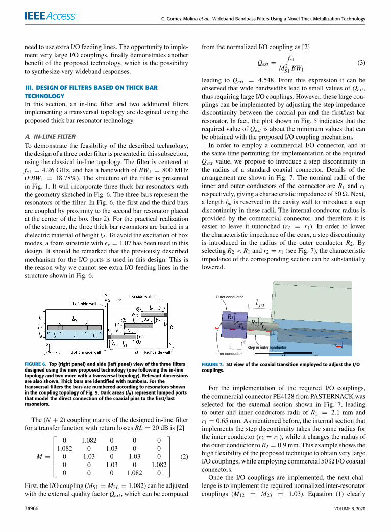
A. IN-LINE FILTERTo demonstrate the feasibility of the described technology,the design of a three order filter is presented in this subsection,using the classical in-line topology. The filter is centered atfc1 = 4.26 GHz, and has a bandwidth of BW1 = 800 MHz(FBW1 = 18.78%). The structure of the filter is presentedin Fig. 1. It will incorporate three thick bar resonators withthe geometry sketched in Fig. 6. The three bars represent theresonators of the filter. In Fig. 6, the first and the third barsare coupled by proximity to the second bar resonator placedat the center of the box (bar 2). For the practical realizationof the structure, the three thick bar resonators are buried in adielectric material of height ld . To avoid the excitation of boxmodes, a foam substrate with εr = 1.07 has been used in thisdesign. It should be remarked that the previously describedmechanism for the I/O ports is used in this design. This isthe reason why we cannot see extra I/O feeding lines in thestructure shown in Fig. 6.
FIGURE 6. Top (right panel) and side (left panel) view of the three filtersdesigned using the new proposed technology (one following the in-linetopology and two more with a transversal topology). Relevant dimensionsare also shown. Thick bars are identified with numbers. For thetransversal filters the bars are numbered according to resonators shownin the coupling topology of Fig. 9. Dark areas (lp) represent lumped portsthat model the direct connection of the coaxial pins to the first/lastresonators.
The (N + 2) coupling matrix of the designed in-line filterfor a transfer function with return losses RL = 20 dB is [2]
M =
0 1.082 0 0 0
1.082 0 1.03 0 00 1.03 0 1.03 00 0 1.03 0 1.0820 0 0 1.082 0
(2)
First, the I/O coupling (MS1 = M3L = 1.082) can be adjustedwith the external quality factor Qext , which can be computed
from the normalized I/O coupling as [2]
Qext =fc1
M2S1 BW1
(3)
leading to Qext = 4.548. From this expression it can beobserved that wide bandwidths lead to small values of Qext ,thus requiring large I/O couplings. However, these large cou-plings can be implemented by adjusting the step impedancediscontinuity between the coaxial pin and the first/last barresonator. In fact, the plot shown in Fig. 5 indicates that therequired value of Qext is about the minimum values that canbe obtained with the proposed I/O coupling mechanism.
In order to employ a commercial I/O connector, and atthe same time permitting the implementation of the requiredQext value, we propose to introduce a step discontinuity inthe radius of a standard coaxial connector. Details of thearrangement are shown in Fig. 7. The nominal radii of theinner and outer conductors of the connector are R1 and r1respectively, giving a characteristic impedance of 50�. Next,a length lju is reserved in the cavity wall to introduce a stepdiscontinuity in these radii. The internal conductor radius isprovided by the commercial connector, and therefore it iseasier to leave it untouched (r2 = r1). In order to lowerthe characteristic impedance of the coax, a step discontinuityis introduced in the radius of the outer conductor R2. Byselecting R2 < R1 and r2 = r1 (see Fig. 7), the characteristicimpedance of the corresponding section can be substantiallylowered.
FIGURE 7. 3D view of the coaxial transition employed to adjust the I/Ocouplings.
For the implementation of the required I/O couplings,the commercial connector PE4128 from PASTERNACKwasselected for the external section shown in Fig. 7, leadingto outer and inner conductors radii of R1 = 2.1 mm andr1 = 0.65 mm. As mentioned before, the internal section thatimplements the step discontinuity takes the same radius forthe inner conductor (r2 = r1), while it changes the radius ofthe outer conductor to R2 = 0.9 mm. This example shows thehigh flexibility of the proposed technique to obtain very largeI/O couplings, while employing commercial 50� I/O coaxialconnectors.
Once the I/O couplings are implemented, the next chal-lenge is to implement the required normalized inter-resonatorcouplings (M12 = M23 = 1.03). Equation (1) clearly
34966 VOLUME 8, 2020
C. Gomez-Molina et al.: Wideband Bandpass Filters Using a Novel Thick Metallization Technology
indicates that wide bandwidths again require very largeinter-resonator couplings (k12 = k23). This large couplingscan be implemented by increasing the thickness of the bars,as detailed in the previous section. Once a proper thicknessvalue is selected for the bar resonators, the inter-resonatorcoupling can be fine adjusted by acting on the variablesx12 = x23 and y12 = y23 of Fig. 6. This is easilyaccomplished by producing charts similar to the one shownin Fig. 4.At this point we should stress that the design of filters
using this coupling matrix approach is only accurate fornarrow band filters. This is because of the intrinsic narrowband approximation implied in deriving the equivalent cir-cuit represented by the coupling matrix (based on lumpedelements and ideally constant impedance or admittanceinverters). Due to dispersive effects in the elements of thereal physical implementation, a final optimization step isneeded to recover the desired target specifications. Afterthis optimization step, the final dimensions of the designedfilter are collected in Table 1. The total size of the filter is35.99 mm × 26.2 mm × 16 mm.
TABLE 1. Physical dimensions of the designed third order in-line filter,according to the sketches shown in Fig. 6 and Fig. 7, with foam as adielectric material (εr = 1.07).
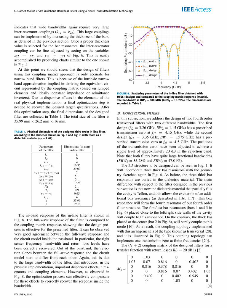
The in-band response of the in-line filter is shown inFig. 8. The full-wave response of the filter is compared tothe coupling matrix response, showing that the design pro-cess is effective for the presented filter. It can be observedvery good agreement between the full-wave response andthe circuit model inside the passband. In particular, the rightcenter frequency, bandwidth and return loss levels havebeen correctly recovered. Out of the passband, the rejec-tion slopes between the full-wave response and the circuitmodel start to differ from each other. Again, this is dueto the large bandwidth of the filter, that introduces, in thephysical implementation, important dispersion effects in res-onators and coupling elements. However, as observed inFig. 8, the optimization process can effectively compensatefor these effects to correctly recover the response inside thebandwidth.
FIGURE 8. Scattering parameters of the in-line filter obtained withHFSS (design) and compared to the coupling matrix response (matrix).The bandwidth is BW1 = 800 MHz (FBW1 = 18.78%). The dimensions arereported in Table 1.
B. TRANSVERSAL FILTERSIn this subsection, we address the design of two fourth ordertransversal filters with two different bandwidths. The firstdesign (fc2 = 3.26 GHz, BW2 = 1.15 GHz) has a prescribedtransmission zero at fz2 = 4.15 GHz, while the seconddesign (fc3 = 3.35 GHz, BW3 = 1.575 GHz) has a pre-scribed transmission zero at fz3 = 4.5 GHz. The positionsof the transmission zeros have been adjusted to achieve aripple level of approximately 20 dB in the rejection band.Note that both filters have quite large fractional bandwidths(FBW2 = 35.28% and FBW3 = 47.01%).The 3D structure to be designed can be seen in Fig. 1. It
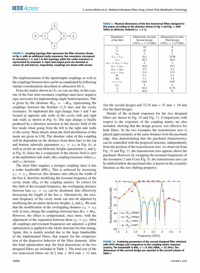
will incorporate three thick bar resonators with the geome-try sketched again in Fig. 6. As before, the three thick barresonators are buried in the dielectric material. The maindifference with respect to the filter designed in the previoussubsection is that now the dielectricmaterial that partially fillsthe cavity is Teflon, and this allows the excitation of an addi-tional box resonance (as described in [16], [17]). This boxresonance will form the fourth resonator of our fourth orderfilter structure. The first/last bar resonators (bars 1 and 3 inFig. 6) placed close to the left/right side walls of the cavitywill couple to this resonance. On the contrary, the thick barplaced at the center (bar 2 in Fig. 6), will barely couple to thismode [16]. As a result, the coupling topology implementedwith this arrangement is of the type known as transversal [20],and it is illustrated in Fig. 9. This coupling topology canimplement one transmission zero at finite frequencies [20].
The (N + 2) coupling matrix of the designed filters for atransfer function with return losses RL = 20 dB is [2]
M1=
0 1.03 0 0 0 0
1.03 0.07 0.816 0 −0.402 00 0.816 0.378 0.816 0 00 0 0.816 0.07 0.402 1.030 −0.402 0 0.402 −0.949 00 0 0 1.03 0 0
(4)
VOLUME 8, 2020 34967
C. Gomez-Molina et al.: Wideband Bandpass Filters Using a Novel Thick Metallization Technology
FIGURE 9. Coupling topology that represents the filter structure shownin Fig. 6, with an additional cavity resonance. Bar resonators correspondto resonators 1, 2, and 3 in this topology, while the cavity resonance isrepresented by resonator 4. Input and output ports are denoted assource (S) and load (L), respectively. Couplings are shown with arrows.
The implementation of the input/output couplings as well asthe couplings between bars can be accomplished by followingsimilar considerations described in subsection III-A.From the matrix shown in (4), we can see that, in this case,
one of the four inter-resonator couplings must have negativesign, necessary for implementing single-band responses. Thisis given by the elements M14 = −M34, representing thecouplings between the first/last (1,3) bars and the cavityresonance. To implement this sign change, bars 1 and 3 arelocated at opposite side walls of the cavity (left and rightside walls as shown in Fig. 6). The sign change is finallyproduced by a direction inversion in the electric field of thebox mode when going from the left to the right side wallsof the cavity. More details about the field distribution of thismode are given in [16]. The absolute value of this couplingwill be dependent on the distance from these bars to the topand bottom sidewalls (parameter yr1 = yr3 in Fig. 6), aswell as on the air and dielectric heights (parameters la and ldin Fig. 6). Since the x-component of the electric field is zeroat the top/bottom side walls, this coupling increases when yr1and yr3 increase.The third filter requires a stronger coupling since it has
a wider bandwidth (BW3). This is achieved by increasingyr1 = yr3. However, this distance also affects the width ofthe box b, therefore modifying the resonant frequency of thecavity mode (M44 of the coupling matrix). To correct forthis shift of the resonant frequency, the overlapping distancebetween bars x12 = x23 can be shortened, thus effectivelydecreasing the length of the box a. Alternatively, the reso-nant frequency of the cavity mode can also be adjusted bymodifying the air and/or dielectric heights, la and ld . We notethat the modification of the overlapping distance x12 = x23will, in turn, change the couplings between barsM12 = M24.However, the effect is compensated, once more, with theadjustment of the separation between them y12 = y23. Afterall couplings and resonant frequencies are adjusted, a globaloptimization is applied to the whole structure for fine tuning.Again, this is mainly needed due to the large bandwidthsof the implemented filters, that require for the compensa-tion of the dispersive behavior of the filter elements. Afterthis final optimization step, the final dimensions of the twodesigned filters are included in Table 2. The total size of thetwo transversal filters are 42.2 mm × 48.6 mm × 12 mm
TABLE 2. Physical dimensions of the two transversal filters designed inthis paper, according to the sketches shown in Fig. 6 and Fig. 7, withTeflon as dielectric material (εr = 2.1).
(for the second design) and 32.76 mm × 51 mm × 18 mm(for the third design).
Details of the in-band responses for the two designedfilters are shown in Fig. 10 and Fig. 11. Comparisons withrespect to the responses of the coupling matrix are alsoincluded, showing that the design process was effective forboth filters. In the two examples the transmission zero isplaced approximately at the same distance from the passbandedge, thus demonstrating that the passband characteristicscan be controlled with the proposed structure, independentlyfrom the position of the transmission zero. As observed fromFig. 10 and Fig. 11, the transmission zero appears above thepassband. However, by swapping the resonant frequencies ofthe resonators 2 and 4 (see Fig. 9), the transmission zero canbe shifted bellow the passband (this is known in the scientificliterature as the zero shifting property).
FIGURE 10. Scattering parameters of the second designed filter obtainedwith HFSS (design) and comparison to the coupling matrix response(matrix). The bandwidth is BW2 = 1.15 GHz (FBW2 = 35.28%). Thedimensions of this second design are reported in the second column ofTable 2.
34968 VOLUME 8, 2020
C. Gomez-Molina et al.: Wideband Bandpass Filters Using a Novel Thick Metallization Technology
FIGURE 11. Scattering parameters of the third designed filter obtainedwith HFSS (design) and comparison to the coupling matrix response(matrix). The bandwidth is BW3 = 1.57 GHz (FBW3 = 47.01%). Thedimensions of this third design are reported in the third column ofTable 2.
To conclude, a comparison between the two last filters interms of spurious free range (SFR) has been performed. Theout of band responses of both filters are compared in Fig. 12.As it can be observed, the SFR of the two filters is similar. Inboth cases, the first spurious band appears at fs1 = 6 GHz,and is due to the excitation of higher order resonances in theshielding cavity. This gives SFR2 ≈ 2.1 GHz (54 %) for thesecond filter and SFR3 ≈ 1.8GHz (43%) for the third design.
FIGURE 12. Comparison for the out of band responses of the two lastdesigned transversal filters from HFSS simulations. Dimensions of bothfilters are collected in Table 2.
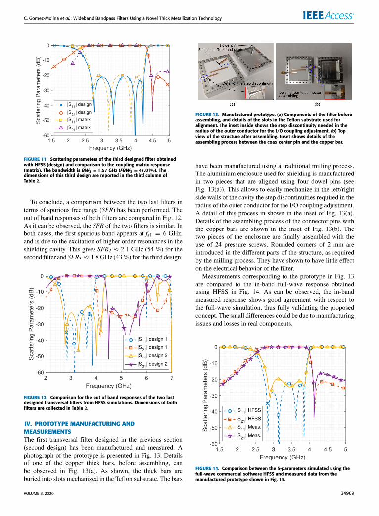
IV. PROTOTYPE MANUFACTURING ANDMEASUREMENTSThe first transversal filter designed in the previous section(second design) has been manufactured and measured. Aphotograph of the prototype is presented in Fig. 13. Detailsof one of the copper thick bars, before assembling, canbe observed in Fig. 13(a). As shown, the thick bars areburied into slots mechanized in the Teflon substrate. The bars
FIGURE 13. Manufactured prototype. (a) Components of the filter beforeassembling, and details of the slots in the Teflon substrate used foralignment. The inset inside shows the step discontinuity needed in theradius of the outer conductor for the I/O coupling adjustment. (b) Topview of the structure after assembling. Inset shows details of theassembling process between the coax center pin and the copper bar.
have been manufactured using a traditional milling process.The aluminium enclosure used for shielding is manufacturedin two pieces that are aligned using four dowel pins (seeFig. 13(a)). This allows to easily mechanize in the left/rightside walls of the cavity the step discontinuities required in theradius of the outer conductor for the I/O coupling adjustment.A detail of this process in shown in the inset of Fig. 13(a).Details of the assembling process of the connector pins withthe copper bars are shown in the inset of Fig. 13(b). Thetwo pieces of the enclosure are finally assembled with theuse of 24 pressure screws. Rounded corners of 2 mm areintroduced in the different parts of the structure, as requiredby the milling process. They have shown to have little effecton the electrical behavior of the filter.
Measurements corresponding to the prototype in Fig. 13are compared to the in-band full-wave response obtainedusing HFSS in Fig. 14. As can be observed, the in-bandmeasured response shows good agreement with respect tothe full-wave simulation, thus fully validating the proposedconcept. The small differences could be due to manufacturingissues and losses in real components.
FIGURE 14. Comparison between the S-parameters simulated using thefull-wave commercial software HFSS and measured data from themanufactured prototype shown in Fig. 13.
VOLUME 8, 2020 34969
C. Gomez-Molina et al.: Wideband Bandpass Filters Using a Novel Thick Metallization Technology
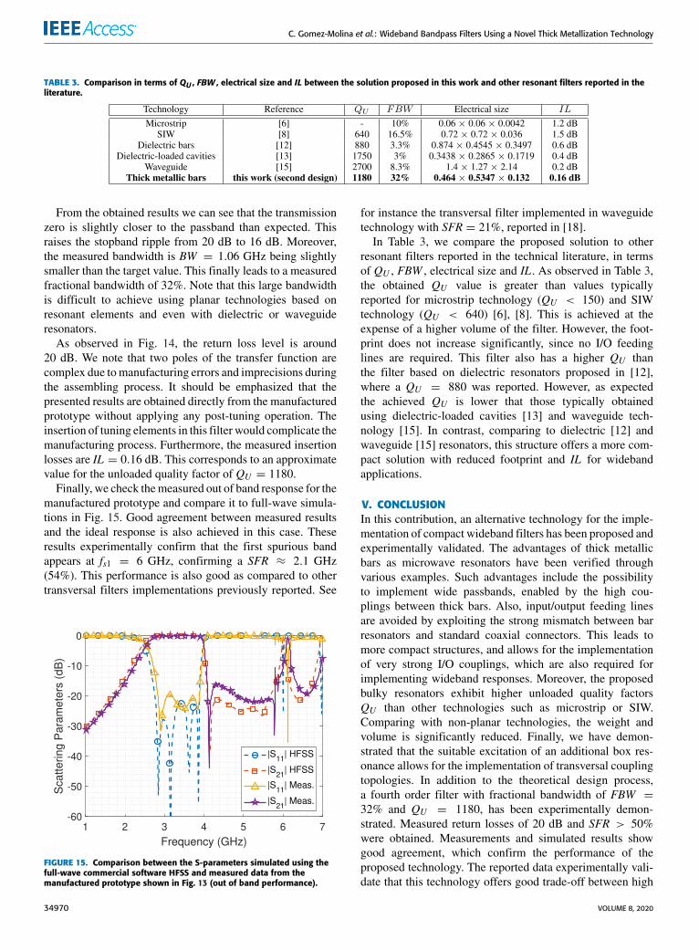
TABLE 3. Comparison in terms of QU , FBW , electrical size and IL between the solution proposed in this work and other resonant filters reported in theliterature.
From the obtained results we can see that the transmissionzero is slightly closer to the passband than expected. Thisraises the stopband ripple from 20 dB to 16 dB. Moreover,the measured bandwidth is BW = 1.06 GHz being slightlysmaller than the target value. This finally leads to a measuredfractional bandwidth of 32%. Note that this large bandwidthis difficult to achieve using planar technologies based onresonant elements and even with dielectric or waveguideresonators.
As observed in Fig. 14, the return loss level is around20 dB. We note that two poles of the transfer function arecomplex due tomanufacturing errors and imprecisions duringthe assembling process. It should be emphasized that thepresented results are obtained directly from the manufacturedprototype without applying any post-tuning operation. Theinsertion of tuning elements in this filter would complicate themanufacturing process. Furthermore, the measured insertionlosses are IL = 0.16 dB. This corresponds to an approximatevalue for the unloaded quality factor of QU = 1180.
Finally, we check themeasured out of band response for themanufactured prototype and compare it to full-wave simula-tions in Fig. 15. Good agreement between measured resultsand the ideal response is also achieved in this case. Theseresults experimentally confirm that the first spurious bandappears at fs1 = 6 GHz, confirming a SFR ≈ 2.1 GHz(54%). This performance is also good as compared to othertransversal filters implementations previously reported. See
FIGURE 15. Comparison between the S-parameters simulated using thefull-wave commercial software HFSS and measured data from themanufactured prototype shown in Fig. 13 (out of band performance).
for instance the transversal filter implemented in waveguidetechnology with SFR = 21%, reported in [18].In Table 3, we compare the proposed solution to other
resonant filters reported in the technical literature, in termsof QU , FBW , electrical size and IL. As observed in Table 3,the obtained QU value is greater than values typicallyreported for microstrip technology (QU < 150) and SIWtechnology (QU < 640) [6], [8]. This is achieved at theexpense of a higher volume of the filter. However, the foot-print does not increase significantly, since no I/O feedinglines are required. This filter also has a higher QU thanthe filter based on dielectric resonators proposed in [12],where a QU = 880 was reported. However, as expectedthe achieved QU is lower that those typically obtainedusing dielectric-loaded cavities [13] and waveguide tech-nology [15]. In contrast, comparing to dielectric [12] andwaveguide [15] resonators, this structure offers a more com-pact solution with reduced footprint and IL for widebandapplications.
V. CONCLUSIONIn this contribution, an alternative technology for the imple-mentation of compact wideband filters has been proposed andexperimentally validated. The advantages of thick metallicbars as microwave resonators have been verified throughvarious examples. Such advantages include the possibilityto implement wide passbands, enabled by the high cou-plings between thick bars. Also, input/output feeding linesare avoided by exploiting the strong mismatch between barresonators and standard coaxial connectors. This leads tomore compact structures, and allows for the implementationof very strong I/O couplings, which are also required forimplementing wideband responses. Moreover, the proposedbulky resonators exhibit higher unloaded quality factorsQU than other technologies such as microstrip or SIW.Comparing with non-planar technologies, the weight andvolume is significantly reduced. Finally, we have demon-strated that the suitable excitation of an additional box res-onance allows for the implementation of transversal couplingtopologies. In addition to the theoretical design process,a fourth order filter with fractional bandwidth of FBW =
32% and QU = 1180, has been experimentally demon-strated. Measured return losses of 20 dB and SFR > 50%were obtained. Measurements and simulated results showgood agreement, which confirm the performance of theproposed technology. The reported data experimentally vali-date that this technology offers good trade-off between high
34970 VOLUME 8, 2020
C. Gomez-Molina et al.: Wideband Bandpass Filters Using a Novel Thick Metallization Technology
performance, compact size and manufacturing complexity,for filters intended for wideband communication systems.
ACKNOWLEDGMENT(Celia Gomez-Molina and Alejandro Pons-Abenza con-tributed equally to this work.)
REFERENCES[1] J.-S. Hong, Microstrip Filters for RF/Microwave Applications. Hoboken,
NJ, USA: Wiley, 2011.[2] R. J. Cameron, C. M. Kudsia, and R. R. Mansour, Microwave Filters
for Communication Systems: Fundamentals, Design and Applications.Hoboken, NJ, USA: Wiley, 2007.
[3] K. T. Jokela, ‘‘Narrow-band stripline or microstrip filters with transmissionzeros at real and imaginary frequencies,’’ IEEE Trans. Microw. TheoryTechn., vol. MTT-28, no. 6, pp. 542–547, Jun. 1980.
[4] D. F. Williams and S. E. Schwarz, ‘‘Design and performance of coplanarwaveguide bandpass filters,’’ IEEE Trans. Microw. Theory Techn., vol. 31,no. 7, pp. 558–566, Jul. 1983.
[5] N. Thomson and J.-S. Hong, ‘‘Compact ultra-widebandmicrostrip/coplanar waveguide bandpass filter,’’ IEEE Microw. WirelessCompon. Lett., vol. 17, no. 3, pp. 184–186, Mar. 2007.
[6] L. Athukorala and D. Budimir, ‘‘Compact filter configurations using con-centric microstrip open-loop resonators,’’ IEEEMicrow. Wireless Compon.Lett., vol. 22, no. 5, pp. 245–247, May 2012.
[7] M. Bozzi, A. Georgiadis, and K. Wu, ‘‘Review of substrate-integratedwaveguide circuits and antennas,’’ IET Microw. Antennas Propag., vol. 5,no. 8, p. 909, 2011.
[8] Z. Liu, G. Xiao, and L. Zhu, ‘‘Triple-mode bandpass filters on CSRR-loaded substrate integrated waveguide cavities,’’ IEEE Trans. Compon.,Packag. Manufact. Technol., vol. 6, no. 7, pp. 1099–1105, Jul. 2016.
[9] A. Belenguer, H. Esteban, and V. E. Boria, ‘‘Novel empty substrate inte-grated waveguide for high-performance microwave integrated circuits,’’IEEE Trans. Microw. Theory Techn., vol. 62, no. 4, pp. 832–839, Apr. 2014.
[10] S. Moscato, C. Tomassoni, M. Bozzi, and L. Perregrini, ‘‘Quarter-modecavity filters in substrate integrated waveguide technology,’’ IEEE Trans.Microw. Theory Techn., vol. 64, no. 8, pp. 2538–2547, Aug. 2016.
[11] L. Silvestri, A. Ghiotto, C. Tomassoni, M. Bozzi, and L. Perregrini, ‘‘Par-tially air-filled substrate integrated waveguide filters with full control oftransmission zeros,’’ IEEE Trans. Microw. Theory Techn., vol. 67, no. 9,pp. 3673–3682, Sep. 2019.
[12] Y.-Y. Zhu, Y.-L. Li, and J.-X. Chen, ‘‘A novel dielectric strip resonatorfilter,’’ IEEE Microw. Wireless Compon. Lett., vol. 28, no. 7, pp. 591–593,Jul. 2018.
[13] L. Pelliccia, F. Cacciamani, C. Tomassoni, and R. Sorrentino, ‘‘Ultra-compact high-performance filters based on TM dual-mode dielectric-loaded cavities,’’ Int. J. Microw. Wireless Technol., vol. 6, no. 2,pp. 151–159, Apr. 2014.
[14] F. M. Vanin, D. Schmitt, and R. Levy, ‘‘Dimensional synthesis for wide-band waveguide filters and diplexers,’’ IEEE Trans. Microw. TheoryTechn., vol. 52, no. 11, pp. 2488–2495, Nov. 2004.
[15] P. Vallerotonda, L. Pelliccia, C. Tomassoni, F. Cacciamani, R. Sorrentino,J. Galdeano, and C. Ernst, ‘‘Compact waveguide bandpass filters forbroadband space applications in c and ku-bands,’’ in Proc. Eur. Microw.Conf. Central Eur. (EuMCE), May 2019, pp. 116–119.
[16] M. Martinez-Mendoza, J. S. Gomez-Diaz, D. Canete-Rebenaque,J. L. Gomez-Tornero, and A. Alvarez-Melcon, ‘‘Design of bandpasstransversal filters employing a novel hybrid structure,’’ IEEE Trans.Microw. Theory Techn., vol. 55, no. 12, pp. 2670–2678, Dec. 2007.
[17] M. Martinez-Mendoza, J. S. Gomez-Diaz, D. Canete-Rebenaque, andA. Alvarez-Melcon, ‘‘Design of dual-bandpass hybrid waveguide–microstrip microwave filters,’’ IEEE Trans. Microw. Theory Techn.,vol. 56, no. 12, pp. 2913–2920, Dec. 2008.
[18] F. J. P. Soler, M. M. F. Mendoza, F. D. Q. Pereira, D. C. Rebenaque,A. A. Melcon, and R. J. Cameron, ‘‘Design of bandpass elliptic fil-ters employing inductive windows and dielectric objects,’’ IEEE Trans.Microw. Theory Techn., vol. 55, no. 11, pp. 2393–2398, Nov. 2007.
[19] High-Frequency Structure Simulator (HFSS), Release 17.2, ANSYS,Canonsburg, PA, USA, 2016. [Online]. Available: https://ansys.com
[20] S. Amari and U. Rosenberg, ‘‘The doublet: A new building block formodular design of elliptic filters,’’ in Proc. 32nd Eur. Microw. Conf.,Oct. 2002, pp. 1–3.
CELIA GOMEZ-MOLINA was born in Murcia,Spain, in 1992. She received the degree in telecom-munication systems from the Technical Universityof Cartagena (UPCT), Murcia, in 2014, and themaster’s degree in telecommunication engineeringin 2016. In 2016, she joined the Department ofInformation Technologies and Communications,UPCT, as a Research Student, where she is cur-rently developing her teaching and research activi-ties. She was a Visiting Student with the University
of California at Davis, Davis, USA, from April 2018 to June 2018, and thePolitecnico di Milano, Italy, from April 2019 to June 2019. She was involvedin the development of analytical and numerical tools for network representa-tions of waveguide and planar discontinuities. Her current scientific interestincludes the design of microwave filters using different technologies.
ALEJANDRO PONS-ABENZA (StudentMember, IEEE) was born in Murcia, Spain,in 1990. He received the Telecommunications Sys-tems Engineer degree and the Ph.D. degree fromthe Technical University of Cartagena (UPCT),in 2014 and 2019, respectively. In 2014, he joinedthe Department of Information Technologies andCommunications, UPCT, as a Research Student.In 2016, he began a research project with theobjective of developing his Ph.D. thesis, as a
collaboration between UPCT and Thales Alenia Space Spain, for the designand development of novel microwave filter structures using additive man-ufacturing techniques for space applications. His current research interestincludes the analysis and design of microwave devices employing additivemanufacturing and synthesis techniques for the design of microwave filters.
JAMES DO received the Master of ElectricalEngineering degree from the University ofVirginia, in 2013, and the Ph.D. degree in mil-limeter wave ground penetrating radar for identi-fying unexploded ordnance from the University ofCalifornia at Davis, in 2019. He was the Lead RFEngineer from the Custom Systems Department,Virginia Diodes Inc., from 2008 to 2014, wherehe designed and tested systems and componentsoperating up to 3THz, including the world’s first
1THz vector network analyzer extension module. He is an RF DesignEngineering Consultant with Virginia Diodes Inc., where he is designing thenext generation of THz Schottky diode frequency multipliers. His master’sthesis was on high directivity THz couplers.
FERNANDO QUESADA-PEREIRA (Member,IEEE) was born in Murcia, Spain, in 1974.He received the Telecommunications EngineerMaster degree from the Technical University ofValencia (UPV), Valencia, Spain, in 2000, andthe Ph.D. degree from the Technical University ofCartagena (UPCT), Murcia, in 2007.
In 1999, he joined the RadiocommunicationsDepartment, UPV, as a Research Assistant, wherehe was involved in the development of numerical
methods for the analysis of anechoic chambers and tag antennas. In 2001,he joined the Communications and Information Technologies Department,UPCT, as a Research Assistant, and then as an Assistant Professor. In 2005,he was a Visiting Scientist with the University of Pavia, Pavia, Italy. In 2009,he was an Invited Researcher with UPV. In 2011, he became an AssociateProfessor with UPCT. His current research interest includes integral equationnumerical methods for the analysis of antennas and microwave devices,along with microwave filters design and applications.
VOLUME 8, 2020 34971
C. Gomez-Molina et al.: Wideband Bandpass Filters Using a Novel Thick Metallization Technology
XIAOGUANG (LEO) LIU (Senior Member, IEEE)received the bachelor’s degree from Zhejiang Uni-versity, Hangzhou, China, in 2004, and the Ph.D.degree from Purdue University, West Lafayette,IN, USA, in 2010. In 2011, he joined the Depart-ment of Electrical and Computer Engineering,University of California at Davis, Davis, CA,USA, as an Assistant Professor, and was promotedto an Associate Professor, in 2017. At the Univer-sity of California at Davis, his research group is
currently investigating various aspects of cutting-edge high-frequency andhigh-speed circuit and system designs.
JUAN SEBASTIAN GOMEZ-DIAZ (SeniorMember, IEEE) was born in Ontur, Spain.He received the M.Sc. and Ph.D. degrees in elec-trical engineering from the Technical Universityof Cartagena, Cartagena, Spain, in 2006 and 2011,respectively.
He is currently an Assistant Professor with theElectrical and Computer Engineering Department,University of California at Davis, Davis. Duringthe development of his Ph.D., he held visiting
research positions with the École Polytechnique de Montréal, Canada andthe Fraunhofer Institute for High Frequency Physics and Radar Techniques,Germany. From October 2011 to March 2014, he was a Postdoctoral Fellowwith the École Polytechnique Fédéral de Lausanne, (EPFL), Switzerland.From May 2014 to August 2016, he continued his postdoctoral work withthe Metamaterials and Plasmonic Research Laboratory, The Universityof Texas at Austin. His main research interests include multidisciplinaryareas of electromagnetic wave propagation and radiation, metamaterialsand metasurfaces, plasmonics, 2-D materials, nonreciprocal and nonlinearphenomena, and other emerging topics on applied electromagnetics andnanotechnology.
Dr. Gomez-Diaz was a recipient of the NSF CAREER Award,the 2017 Leopold Felsen Award for Excellence in Electrodynamics, the RajMittra Award presented by the 2015 IEEE Antennas and PropagationSociety, the Young Scientist Award of the 2015 URSI Atlantic RadioScienceConference, the FP7 Marie Curie Fellowship from the European Com-mission, in 2012, the Colegio Oficial de Ingenieros de Telecomunicación(COIT/AEIT) Award to the Best Spanish Ph.D. Thesis in basic informationand communication technologies, in 2011, and the Best Ph.D. Thesis Awardfrom the Technical University of Cartagena. He serves as a Reviewer forseveral journals on antennas, microwaves/THz, and physics.
ALEJANDRO ALVAREZ-MELCON (SeniorMember, IEEE) was born in Madrid, Spain,in 1965. He received the TelecommunicationsEngineer degree from the Technical University ofMadrid (UPM), Madrid, Spain, in 1991, and thePh.D. degree in electrical engineering from theSwiss Federal Institute of Technology, Lausanne,Switzerland, in 1998. In 1988, he joined the Sig-nal, Systems and Radio Communications Depart-ment, UPM, as a Research Student, where he was
involved in the design, testing, and measurement of broad-band spiral anten-nas for electromagnetic measurements support (EMS) equipment. From1991 to 1993, he was with the Radio Frequency Systems Division, EuropeanSpace Agency (ESA/ESTEC), Noordwijk, The Netherlands, where he wasinvolved in the development of analytical and numerical tools for the study ofwaveguide discontinuities, planar transmission lines, and microwave filters.From 1993 to 1995, he was with the Space Division, Industry AlcatelEspacio, Madrid, Spain. He was with ESA, where he collaborated in severalESA/European Space Research and Technology Centre (ESTEC) contracts.From 1995 to 1999, he was with the Swiss Federal Institute of Technology,École Polytechnique Fédérale de Lausanne (EPFL), Lausanne, Switzerland,where he was involved with the field of microstrip antennas and printedcircuits for space applications. In 2000, he joined the Technical Universityof Cartagena, Spain, where he is currently developing his teaching andresearch activities. He was an Invited Professor with the PolytechniqueUniversity of Montreal Canada, from July 2010 to September 2010, and aVisiting Professor with the University of California at Davis, Davis, USA,from October 2017 to September 2018. He was a recipient of the JournéeInternationales de Nice Sur les Antennes (JINA) Best Paper Award for thebest contribution to the JINA’98 International Symposium on Antennas,and the Colegio Oficial de Ingenieros de Telecomunicación (COIT/AEIT)Award to the best Ph.D. dissertation in basic information and communicationtechnologies.
34972 VOLUME 8, 2020


