Embed Size (px)
Citation preview
NASA Conference Publication 3290-,/c-'_.- I
NASA-CP-3290-VOL- 119960000230
Proceedings of the Fourth InternationalConference and Exhibition: World Congresson Superconductivity
Volume I
Proceedingsof a conferenceand exhibitionheldat MarriottOrlandoWorldCenter,Orlando,Florida,June 27-July I, 1994

I'NASA Technical Ubrary
NASAConference Publication 32903 1176014204029
@Proceedings of the Fourth InternationalConference and Exhibition: World Congresson Superconductivity
Volume I
Kumar Krishen and Calvin Burnham, Editors
Lyndon B. Johnson Space CenterHouston, Texas
Proceedings of a conferenceand exhibitionheld atMarriott Orlando WorldCenter,Orlando, Florida,June 27 -July 1, 1994
1994

This publication is available from the NASA Center for AeroSpaceInformation, 800 Elkridge Landing Road, Linthicum Heights,
MD 21090-2934 (301)621-0390.

The WorldCongresson Superconductivity
The World Congress on Superconductivity (WCS) was formed in Houston in1987 by a group of volunteer engineers and scientists interested in increasing thefocus on this emerging technology field of superconductivity. The leadership of theWCS, a non-profit 501(c)3 organization, is comprised of individuals from several majortechnical societies such as the Engineers Council of Houston, the American ChemicalSociety, IEEE, etc. This group is augmented by leaders of the international research,academic, science, government and business communities who serve on the AdvisoryBoard or ad hoc committees. Since its inception, the Advisory Board has been globalin scope with technologists from such countries as Japan, Russia, Switzerland, etc.,actively involved in steering the direction of our programs.
The goals of the WCS have been to establish and foster the development andcommercial application of superconductivity technology on a global scale by providinga non-adversarial, non-advocacy forum where scientists, engineers, businessmen andgovernment personnel can freely exchange information and ideas on recentdevelopments and directions for the future of superconductive research.
To date, four internationalconferences have been completed since 1987.These conferences were attended by over fifteen hundred delegates from thirty-sixnations. The success of these conferences is remarkable in light of the fact that theWCS has no staff and must rely on monetary donations from the private sector,foundations and government agencies. In addition, thousands of man-hours havebeen donated by the WCS volunteer staff in the organizing of this activities. WCS isespecially thankful for the assistance of Dr. Kumar Krishen as program chairman andthe support from NASA which makes this activity possible.
Because of the unique nature of the WCS and its success, the organization issanctioned by the United Nations and is a member of the UN's Advance TechnologyAlert System. The WCS was awarded Leadership Houston's International Corporateaward for its Munich conference in 1992.
Plansare currentlyunderway for the 5th InternationalConference of the WorldCongress on Superconductivity, which will be held in July 1996 in Budapest, Hungary.This meeting will coincide with the 1,100 year anniversary of Hungary. For moreinformation on this meeting and WCS activities, please contact Calvin Burnham,President, World Congress on Superconductivity, P.O. Box 27805, Houston, TX77227-7805; telephone 713-895-2500; fax 713-469-5788;e-mail: [email protected]
iii

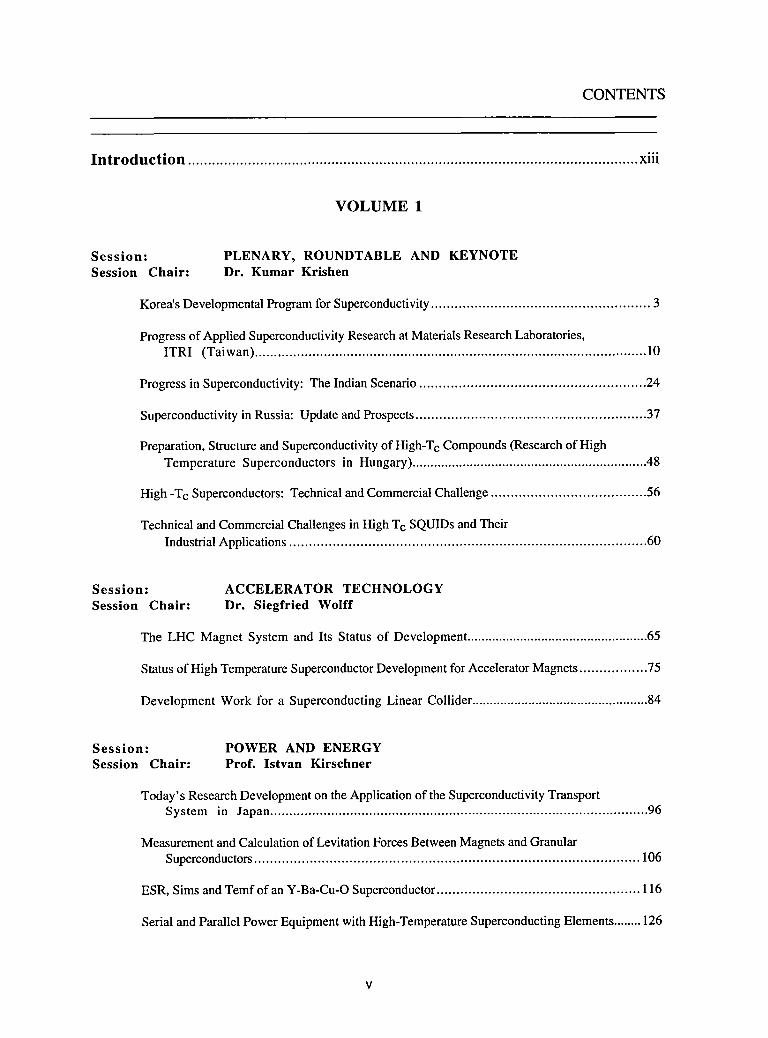
CONTENTS
Introduction .................................................................................................................xiii
VOLUME 1
Session: PLENARY, ROUNDTABLE AND KEYNOTESession Chair: Dr. Kumar Krishen
Korea'sDevelopmentalProgramforSuperconductivity....................................................... 3
Progressof AppliedSuperconductivityResearchatMaterialsResearchLaboratories,ITRI (Taiwan) ...................................................................................................... 10
Progressin Superconductivity:The IndianScenario ......................................................... 24
Superconductivityin Russia: UpdateandProspects.......................................................... 37
Preparation, Structure and Superconductivityof High-Tc Compounds (Research of HighTemperature Superconductors in Hungary) ................................................................. 48
High -Tc Superconductors: Technical and Commercial Challenge ....................................... 56
Technical and Commercial Challenges in High Tc SQUIDs and TheirIndustrial Applications .......................................................................................... 60
Session: ACCELERATOR TECHNOLOGY
Session Chair: Dr. Siegfried Wolff
The LHC Magnet System and Its Status of Development ................................................... 65
Status of High Temperature SuperconductorDevelopment for Accelerator Magnets ................. 75
Development Work for a Superconducting Linear Collider .................................................. 84
Session: POWER AND ENERGYSession Chair: Prof. Istvan Kirschner
Today's Research Development on the Application of the Superconductivity TransportSystem in Japan ................................................................................................... 96
Measurement and Calculation of LevitationForces BetweenMagnets and GranularSuperconductors................................................................................................. 106
ESR, Sims and Temf of an Y-Ba-Cu-O Superconductor................................................... 116
Serial and Parallel Power Equipment with High-Temperature Superconducting Elements........126
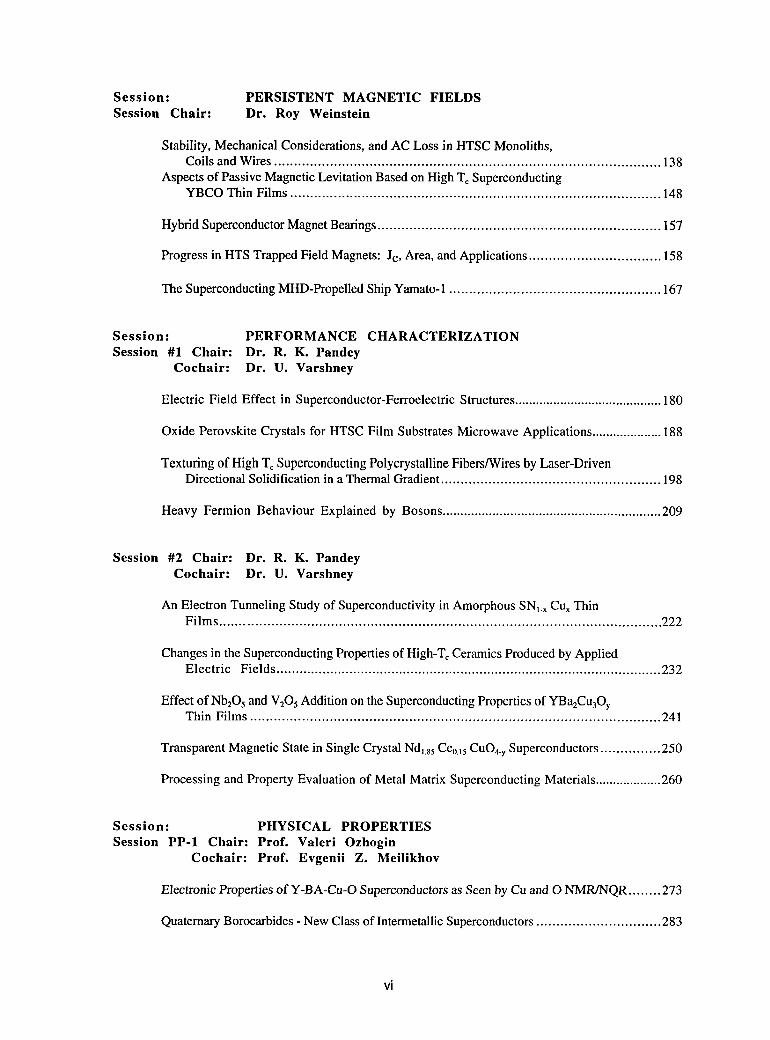
Session: PERSISTENT MAGNETIC FIELDSSession Chair: Dr. Roy Weinstein
Stability, Mechanical Considerations, and AC Loss in HTSC Monoliths,Coils and Wires ................................................................................................. 138
Aspects of Passive Magnetic Levitation Based on High TcSuperconductingYBCO Thin Films ............................................................................................. 148
Hybrid SuperconductorMagnet Beatings....................................................................... 157
Progress in HTS Trapped Field Magnets: Jc, Area, and Applications................................. 158
The Superconducting MHD-Propelled Ship Yamato-1 ..................................................... 167
Session: PERFORMANCE CHARACTERIZATION
Session #1 Chair: Dr. R. K. PandeyCochair: Dr. U. Varshney
Electric Field Effect in Superconductor-Ferroelectric Structures .......................................... 180
Oxide Perovskite Crystals for HTSC Film Substrates Microwave Applications .................... 188
Texturing of High TcSuperconducting Polycrystalline Fibers/Wires by Laser-DrivenDirectional Solidification in a Thermal Gradient ....................................................... 198
Heavy Fermion Behaviour Explained by Bosons ............................................................. 209
Session #2 Chair: Dr. R. K. PandeyCochair: Dr. U. Varshney
An Electron Tunneling Study of Superconductivity in Amorphous SN_.xCUxThinFilms ............................................................................................................... 222
Changes in the Superconducting Propertiesof High-T¢Ceramics Produced by AppliedElectric Fields .................................................................................................... 232
Effect of Nb205and V205Addition on the Superconducting Properties of YBa2Cu3OyThin Films ....................................................................................................... 241
Transparent Magnetic State in Single Crystal Nd_85Ce015CuO4.ySuperconductors ............... 250
Processing and Property Evaluation of Metal Matrix Superconducting Materials ................... 260
Session: PHYSICAL PROPERTIESSession PP-1 Chair: Prof. Valeri Ozhogin
Cochair: Prof. Evgenii Z. Meilikhov
Electronic Properties of Y-BA-Cu-O Superconductors as Seen by Cu and O NMR/NQR ........ 273
Quaternary Borocarbides - New Class of Intermetallic Superconductors............................... 283
vi
Electronic Structure and the Van Hove Singularity ScenarioinHigh-TcHgBa2CuO4+_Superconductors................................................................ 298
Boson Localization and Universality in Yna2Cu3.xMxOT. _ ................................................. 308
Thermomagnetic Phenomena in the Mixed State of High Temperature Superconductors......... 318
Spectroscopy of Infrared-Active Phonons in High-TemperatureSuperconductors................... 328
Session PP-2 Chair: Prof. Valeri OzhoginCochair: D. Brinkman
Flux Pinning Characteristics and Irreversibility Line in High TemperatureSuperconductors................................................................................................. 337
Effects of Neutron Irradiation on the London Penetration Depth for PolycrystallineBil.8Pb0.3Sr2Ca2Cu30i0 Superconductor ............................................................... 347
The Thermopower in the Temperature Range T:1000K and the Band Spectrum ofBi-Based Superconductors ..................................................................................... 354
Nonequilibrium Transport in SuperconductingFilaments ................................................. 359
Session: FABRICATION METHODOLOGYSession Chair: Dr. U. Balachandran
High Tc Superconductors Fabricated by PlasmaAerosol Mist Deposition Technique ............. 372
Partial Melting of Bulk Bi-2212 .................................................................................. 382
Correlation Between Fabrication Factor and SuperconductingProperties of theT1-and Bi- Based HighTc Superconductor............................................................... 391
VOLUME 2
Session: SUPERCONDUCTIVE MAGNETIC ENERGYSTORAGE (SMES) UTILITY INTEREST GROUP
Session Chair Dr. Phillip BaumannSMESI: Technical Session
Policy Issues Inherentin AdvancedTechnologyDevelopment........................................... 400
SMES 2: Technical Session
Financial Options Methodologyfor Analyzing Investmentsin New Technology .................. 405
SMES: Redefining the Path to Commercial Demonstration ............................................. 410
Modular Transportable Superconducting Magnetic Energy Systems .................................... 416
vii
Session: THIN FILMSSession Chair: Prof. Tomoji Kawai
Optimizationof the DepositionConditionsandStructuralCharacterizationofYi Ba2Cu30T.x Thin Superconducting Films............................................................ 423
Growth andAnalysisof Highly Oriented(1ln)BCSCOFilms forDevice Research............... 433
Structural, Transport and Microwave Properties of 1231SapphireFilms:Thickness Effect ................................................................................................. 440
Scanning Micro-Hall Probe Mapping of Magnetic Flux Distributions and CurrentDensities in YBazCu307 Thin Films ...................................................................... 447
Angular Dependence of Critical Current Density and MagnetoresistanceofSputtered High-T:Films ...................................................................................... 457
Correlations Between Critical Current Density, Jc,Critical Temperature, To,andStructural Quality of YiB2Cu307.x Thin Superconducting Films .................................. 467
Session: HIGH TEMPERATURE MATERIALSSession #1 Chair: Prof. Mikio Takano
The Oxygen Content of the High-TemperatureSuperconducting CompoundBi2+xSR3_yCayCu2Os+dwith Respect to Varying Ca and Bi Contents ............................ 483
PbSolubility of the High-Temperature Superconducting Phase Bi2Sr2Ca2Cu30_0.d..........................490
Superconductivity Theory Applied to the Periodic Table of Elements ................................. 500
Chemical Stabilization and High Pressure Synthesis of B:Free Hg-BasedSuperconductors, (Hg, M) Sr2Can.lCunOy(n = 1-3) .................................................. 510
Session #2 Chair: K. Kishio
A New Series of Oxycarbonate Superconductors (CuosC0.5)mBam+lCan_l CunO2(m+n)+l ............. 522
High Pressure Synthesis and Magnetic Studies of Quasi One Dimensional SystemsSr,.i CU°.l02. (n = 3, 5)...................................................................................... 529
Influence of Calcium on Transport Properties,Band Spectrum and Superconductivityof YBa2Cu3Oy and YBal.5La0.sCu3Oy.................................................................... 537
Structure and Superconductivity in (Bio.3s Cu0.65) Sr2YCu207 and Related Materials ............... 546
Structural, Dynamical and Electronic Properties of CaCuO2.............................................. 555
viii
Session: DEVICE APPLICATIONSSession Chair: Dr. Yoshifusa Wada
High-Performance Passive Microwave Survey on Josephson Junctions ............................... 568
Josephson Frequency Meter for Millimeter and Submillimeter Wavelengths ........................ 574
Josephson Junction Spectrum Analyzer for Millimeter and Submillimeter Wavelengths.........585
Nondestructive Testing (NDT) of Metal Cracks Using a High Tcrf-SQUID andEddy CurrentMethod .......................................................................................... 594
High Temperature Superconductors Applications in Telecommunications ............................ 601
HTS Thin Films: Passive Microwave Components and Systems Integration Issues ............. 611
Session: WIRE FABRICATIONSession Chair: Dr. K. C. Goretta
Development of Practical High TemperatureSuperconductingWire for ElectricPower Applications ............................................................................................ 624
Mechanical Properties of High-TemperatureSuperconductingWires ................................... 633
Progress in Developmentof Tapes and Magnets Made From Bi-2223 Superconductors .......... 639
High Temperature Superconductors as a Technological Discontinuity in the PowerCable Industry ................................................................................................... 650
Improvement of Critical Current Density in Thallium-Based (T1,Bi)Sr_6Bao.nCa2Cu30 xSuperconductors................................................................................................. 661
Session: GRANULAR SUPERCONDUCTORSSession Chair: Prof. Manu S. Multani
Introduction of Artificial Pinning Centres in "Bi2Sr2CaCu208'' Ceramics............................. 677
Tape Casting and Partial Melting of Bi-2212 Thick Films ............................................... 686
Effect of Microwave-EnhancedSuperconductivityin YBa2Cu307 Bi-Crystalline GrainBoundary Weak-Links......................................................................................... 694
Effects of Oxygen Stoichiometry on the Scaling Behaviors of YBa2Cu3Ox GrainBoundary Weak-Links......................................................................................... 703
Effect of Particle Size and Particle Size Distribution on Physical Characteristics,Morphology and Crystal Structure of Explosively Compacted High-ToSuperconductors................................................................................................. 712
ix
Percolation Effect in Thick Film Superconductors (Using a Bi(Pb)SrCaCuO BasedPaste to Prepare a Superconducting Planar Transformer) ............................................. 722
Line Group Techniques in Description of the Structural Phase Transitions inSomeSuperconductors ........................................................................................ 730
Session: POSTERS
Macroscopic and Bulk-Controlled Elastic Modes in an Interaction of Interstitial AlcaliMetal Cations Within a Face-Centered Cubic Crystalline Fullerine .............................. 739
Thallium 2223 High Tc Superconductor in a Silver Matrix and Its Magnetic Shielding,Hermal Cycle and Time Aging Properties ............................................................... 743
The Role of Silver in the Processing and Properties of Bi-2212 ......................................... 753
A Study on the Superconducting Properties of YBa2Cu3_xNbxOyThin Films ....................... 762
Growth and Micro Structural Studies on Yittria Stabilized Zirconia (YSZ) and StrontiumTitanate (STO) Buffer Layers................................................................................ 770

I
INTRODUCTION

INTRODUCTION
The World Congress on Superconductivity(WCS) is a nonprofitorganization dedicated tothe universal promotion of research, development, and applications of superconductivitytechnology. Through open meetings and conferences, it provides forums for the worldcommunity to share technologicaland research results in the field of superconductivity andto discuss the translation of these results into applicationswhich will benefit all of theworld's population. The WCS established the Award of Excellence to recognize thecontributions of organizations and individuals within the industry. Since 1988,nineteenindividuals and organizationshave received this recognition.
The WCS presented its first two InternationalConferences and Exhibition WorldCongresses on Superconductivity in 1988 and 1990,with a combined attendance ofapproximately 1,000 delegates from 16 countries. Its third conference, attended by morethan 400 scientists, technologists, and managers from thirty six nations, was held inMunich, Germany in September 1992. Proceedingsfrom these three conferences havebeen published and distributed worldwide.
The Fourth International Conference and ExhibitionWorld Congresson Superconductivitywas held June 27-July 1, 1994 in Orlando, Florida. It was sponsored in large part by theNational Aeronautics and Space Administration's Johnson Space Center. More than 120presentations were scheduled for the more than 200 delegates from 30 nations whoattended this year's conference. I believe this conference providedthe most comprehensiveworldwide review of high temperature superconductivityresearch and its applicationstodate (table 1). The exchange of informationand ideas and the identificationof technical andcommercial challenges which occurred during the conferenceare bound to significantlyadvance this revolutionary technology.
The substantial progress which has been made in the field of superconductivitywasreflected in the conferencepresentations: the numberof elementsused in the search ofsuperconductivityhas increased to eight; the reportedcriticaltemperatureshave increased to164°K;and a new thallium-based compound, reported by Professor Z.Z. Sheng, isexpected to provide further insight into the mechanismsthat govern the complexphenomena of superconductivity. Additionally, significantprogress was reported withtheoretical and modeling efforts which will accelerateresearchand developmentof newmaterials and devices, and with magnetic field capacityand electricalcurrent capacity. Theparameters for these capacities are now quoted at 77°K at 2.2 Tesla and 100,000Amps/cm2, respectively.
The commercial applications of superconductivityare progressingrapidly, with magnets,SQUIDS, transformers, thin films, wires, and several devices now available commercially.And the worldwide interest in the exploration of this revolutionarytechnology continues togrow.
To create the uniquely efficient superconductormany productioncomponents must beorchestrated. Teaming the exact mix and proportionof elements,arranging the differentlayers of elements in the appropriateorder, and achieving the fightenvironment andtemperatures in which to cook the elementsare essential.
Any technology which enhances our quality of life truly is super and I believesuperconductivity will dojust that. This revolutionary technology will be an integral partof future achievements which will produce greatbenefits for humans.
°..
XlU
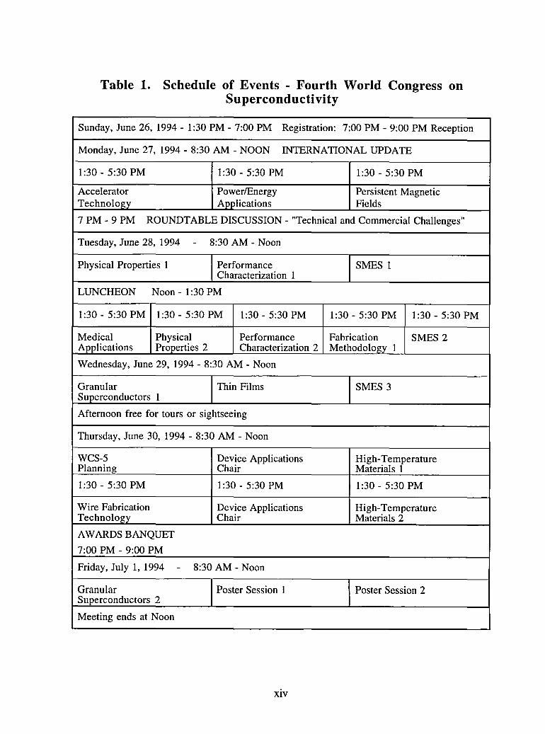
Table 1. Schedule of Events - Fourth World Congress onSuperconductivity
Sunday, June 26, 1994 - 1:30 PM - 7:00 PM Registration: 7:00 PM - 9:00 PM Reception
Monday, June 27, 1994 - 8:30 AM - NOON INTERNATIONAL UPDATE
1:30 - 5:30 PM 1:30 - 5:30 PM 1:30 - 5:30 PM
Accelerator Power/Energy PersistentMagneticTechnology Applications Fields
7 PM - 9 PM ROUNDTABLE DISCUSSION - "Technical andCommercial Challenges"
Tuesday, June 28, 1994 8:30 AM - Noon
Physical Properties 1 Performance SMES 1Characterization1
LUNCHEON Noon - 1:30 PM
1:30 - 5:30 PM 1:30 - 5:30 PM 1:30 - 5:30 PM 1:30 - 5:30 PM 1:30 - 5:30 PM
Medical Physical Performance Fabrication SMES 2Applications Properties 2 Characterization 2 Methodology 1
Wednesday, June 29, 1994 - 8:30 AM - Noon
Granular Thin Films SMES 3Superconductors 1
Afternoon free for tours or sightseeing
Thursday, June 30, 1994 - 8:30 AM - Noon
WCS-5 Device Applications High-TemperaturePlanning Chair Materials 1
1:30 - 5:30 PM 1:30 - 5:30 PM 1:30 - 5:30 PM
Wire Fabrication Device Applications High-TemperatureTechnology Chair Materials 2
AWARDS BANQUET7:00 PM - 9:00 PM
Friday, July 1, 1994 8:30 AM - Noon
Granular Poster Session 1 Poster Session 2Superconductors 2
Meeting ends at Noon
xiv
The process involved in developing superconductorsis an excellent exampleof the greatresults that can be achievedby successfully teaming differentelements. It shouldsymbolize for us the advances we are capable of when we work together. Most of thetechnological advances made in this field in recent years are the result of teamwork. One ofthe objectives of this conference was to promote globalteaming which transcendedgeographic and nationalbarriers and helpedto advance science and technology related tosuperconductivity. Since we collectivelyshare the challengeof advancing teamwork andcooperation, we hope that several dialogues were initiated during this conference.
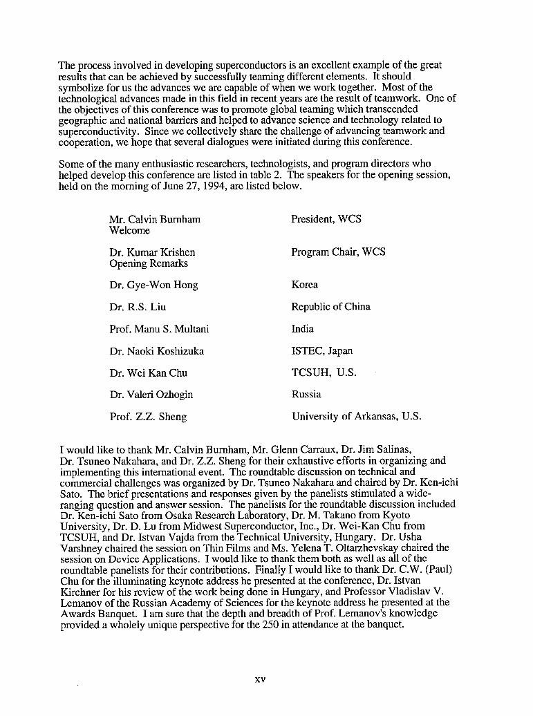
Some of the many enthusiastic researchers, technologists, and program directors whohelped develop this conference are listed in table 2. The speakers for the opening session,held on the morning of June 27, 1994, are listed below.
Mr. Calvin Burnham President, WCSWelcome
Dr. Kumar Krishen Program Chair, WCSOpening Remarks
Dr. Gye-Won Hong Korea
Dr. R.S. Liu Republic of China
Prof. Manu S. Multani India
Dr. Naoki Koshizuka ISTEC, Japan
Dr. Wei Kan Chu TCSUH, U.S.
Dr. Valeri Ozhogin Russia
Prof. Z.Z. Sheng University of Arkansas, U.S.
I would like to thank Mr. Calvin Burnham, Mr. Glenn Carraux, Dr. Jim Salinas,Dr. Tsuneo Nakahara, and Dr. Z.Z. Sheng for their exhaustive efforts in organizing andimplementing this internationalevent. The roundtable discussion on technical andcommercial challenges was organized by Dr. Tsuneo Nakahara and chaired by Dr. Ken-ichiSato. The brief presentations and responsesgiven by the panelists stimulated a wide-ranging question and answer session. The panelists for the roundtable discussion includedDr. Ken-ichi Sato from Osaka Research Laboratory, Dr. M. Takano from KyotoUniversity, Dr. D. Lu from Midwest Superconductor, Inc., Dr. Wei-Kan Chu fromTCSUH, and Dr. Istvan Vajda from the Technical University, Hungary. Dr. UshaVarshney chaired the session on Thin Films and Ms. Yelena T. Oltarzhevskay chaired thesession on Device Applications. I would like to thank them both as well as all of theroundtable panelists for their contributions. Finally I would like to thank Dr. C.W. (Paul)Chu for the illuminating keynote address he presented at the conference, Dr. IstvanKirchner for his review of the work being done in Hungary, and Professor Vladislav V.Lemanov of the Russian Academy of Sciences for the keynote address he presented at theAwards Banquet. I am sure that the depth and breadth of Prof. Lemanov's knowledgeprovided a wholely unique perspective for the 250 in attendance at the banquet.
xv
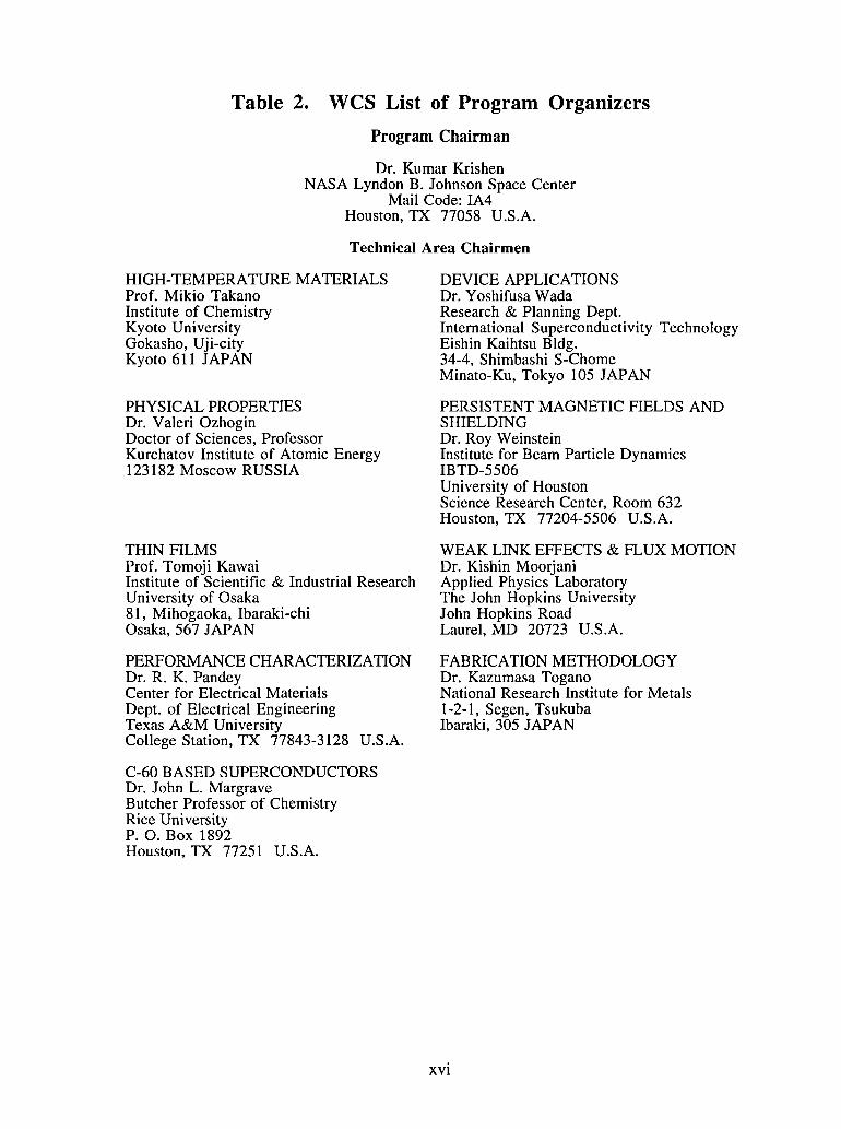
Table 2. WCS List of Program Organizers
Program Chairman
Dr. Kumar KrishenNASA Lyndon B. Johnson Space Center
Mail Code: IA4Houston, TX 77058 U.S.A.
Technical Area Chairmen
HIGH-TEMPERATURE MATERIALS DEVICE APPLICATIONSProf. Mikio Takano Dr. Yoshifusa WadaInstitute of Chemistry Research & Planning Dept.Kyoto University International Superconductivity TechnologyGokasho, Uji-city Eishin Kaihtsu Bldg.Kyoto 611 JAPAN 34-4, Shimbashi S-Chome
Minato-Ku, Tokyo 105 JAPAN
PHYSICAL PROPERTIES PERSISTENT MAGNETIC FIELDS ANDDr. Valeri Ozhogin SHIELDINGDoctor of Sciences, Professor Dr. Roy WeinsteinKurchatov Institute of Atomic Energy Institute for Beam Particle Dynamics123182 Moscow RUSSIA IBTD-5506
University of HoustonScience Research Center, Room 632Houston, TX 77204-5506 U.S.A.
THIN FILMS WEAK LINK EFFECTS & FLUX MOTIONProf. Tomoji Kawai Dr. Kishin MoorjaniInstitute of Scientific & Industrial Research Applied Physics LaboratoryUniversity of Osaka The John Hopkins University81, Mihogaoka, Ibaraki-chi John Hopkins RoadOsaka, 567 JAPAN Laurel, MD 20723 U.S.A.
PERFORMANCE CHARACTERIZATION FABRICATION METHODOLOGYDr. R. K. Pandey Dr. Kazumasa ToganoCenter for Electrical Materials National Research Institute for MetalsDept. of Electrical Engineering 1-2-1, Segen, TsukubaTexas A&M University Ibaraki, 305 JAPANCollege Station, TX 77843-3128 U.S.A.
C-60 BASED SUPERCONDUCTORSDr. John L. MargraveButcher Professor of ChemistryRice UniversityP. O. Box 1892Houston, TX 77251 U.S.A.
xvi
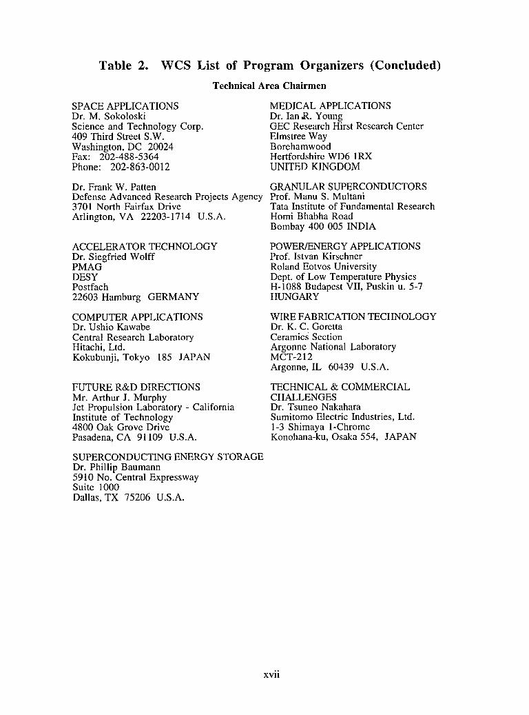
Table 2. WCS List of Program Organizers (Concluded)
Technical Area Chairmen
SPACE APPLICATIONS MEDICAL APPLICATIONSDr. M. Sokoloski Dr. Ian_R.YoungScience and Technology Corp. GEC Research Hirst Research Center409 Third Street S.W. Elmstree WayWashington, DC 20024 BorehamwoodFax: 202-488-5364 Hertfordshire WD6 1RXPhone: 202-863-0012 UNITED KINGDOM
Dr. Frank W. Patten GRANULAR SUPERCONDUCTORSDefense Advanced Research Projects Agency Prof. Manu S. Multani3701 North Fairfax Drive Tata Institute of Fundamental ResearchArlington, VA 22203-1714 U.S.A. Homi Bhabha Road
Bombay 400 005 INDIA
ACCELERATOR TECHNOLOGY POWER/ENERGYAPPLICATIONSDr. Siegfried Wolff Prof. Istvan KirschnerPMAG Roland Eotvos UniversityDESY Dept. of Low Temperature PhysicsPostfach H-1088 Budapest VII, Puskin u. 5-722603 Hamburg GERMANY HUNGARY
COMPUTER APPLICATIONS WIRE FABRICATION TECHNOLOGYDr. Ushio Kawabe Dr. K. C. GorettaCentral Research Laboratory Ceramics SectionHitachi, Ltd. Argonne National LaboratoryKokubunji, Tokyo 185 JAPAN MCT-212
Argonne, IL 60439 U.S.A.
FUTURE R&D DIRECTIONS TECHNICAL & COMMERCIALMr. Arthur J. Murphy CHALLENGESJet Propulsion Laboratory - California Dr. Tsuneo NakaharaInstitute of Technology Sumitomo Electric Industries, Ltd.4800 Oak Grove Drive 1-3 Shimaya 1-ChromePasadena, CA 91109 U.S.A. Konohana-ku, Osaka 554, JAPAN
SUPERCONDUCTING ENERGY STORAGEDr. Phillip Baumann5910 No. Central ExpresswaySuite 1000Dallas, TX 75206 U.S.A.
xvii
Throughout my thirty year career, first with Kansas State University, then with LockheedElectronics Company and now with the National Aeronauticsand Space Administration(NASA), I have supported the space program. The paramount missions of NASA havealways ignited my imagination and my determination. Today one of the key missions forNASA is researching the universe: its origin and growth, its formation of bodies andsystems, and its governing processes. Another mission of this Agency is to explore theevolution of life within the universe. Through the efforts of many nations, we have cometo realize the critical link between human life and the global environment,and, as anextension of this, between the phenomena that underlie the nature of our universe.NASA's current mission addresses the need to expand our knowledge about our universe,as does research in the area of superconductivity. This research will provide a means tocharacterize unique phenomena which might otherwisebe unobservable. We hope thatthese proceedings will help identify ways to advance the performance and applications ofhigh temperature superconductors.
Kumar Krishen, Ph.D.Program ChairmanWorld Congress on Superconductivity
°°°
XVlll
Plenary, Roundtable, and KeynoteEll
Chair: Dr. Kumar Krishen

Korea's Developmental Program for Superconductivity
Gye-wonHong, Dong-YeonWon, II-HyunKuk,Jong-ChulPark*
Korea Atomic Energy Research Institute
P.O. Box 105, Yuseong, Taejeon,305-600, Korea*Korea Standards Research Institute
P.O. Box 102, Yuseong, Taejeon,305-600,Korea
1. Introduction
Superconductivityresearchin Korea was firstlycarriedout in the late
70s by a researchgroupin SeoulNationalUniversity(SNU), who fabricateda
smallscale superconductingmagneticenergystoragesystemunderthe financial
supportfrom Korea ElectricPower Company(KEPCO). But a few researchers
were involved in superconductivityresearch until the oxide high Tc
superconductorwas discoveredby Bednorzand Mueller.1)
After the discoveryof YBaCuO superconductoroperatingabove the boiling
point of liquid nitrogen(77K)2), Korean Ministryof Scienceand Technology(
MOST) sponsoreda specialfund for the highTc superconduclJvityresearchto
universitiesand national research institutesby recognizingits importance.
Scientists engaged in this project organized "High Temperature
SuperconductivityResearchAssociation(HITSRA)" for effectiveconductingof
research.Its major functionsare to coordinateresearchactivitieson high Tc
superconductivityand organizethe workshopfor activeexchangeof information.
Duringlast sevenyears the major superconductivityresearchhas beencarried
out through the coordinationof HITSRA. The major parts of the Korea's
superconductivityresearch program were related to high temperature
superconductorand only a few groups were carrying out research on
conventionalsuperconductortechnology,and Korea Atomic Energy Research
Institute(KAERI)and Korea ElectrotechnologyResearchInstitute(KERI)have
led this research.3
In this talk, the current status and future plans of superconductivity
researchin Korea will be reviewedbasedon the resultspresentedin interim
meetingof HITSRA, April 1-2, 1994, Taejeon,as well as the researchactivity
of KAERI.
2. Research Activities in Korea
After the first workshopheld on July 6, 1987, HITSRA has organized
18 workshopsto promoteresearchactivitieson high Tc superconductivityand
share the results. Recent researchresults presentedat interimmeeting of
HITSRA are summarizedas follows:
(1) film : High qualityYBCO thin films were reportedby many groups
using RF sputtering,laser ablation,chemicalvapor depositionetc. But there
was no reporton Bi- and TI-basedthinfilm. Currentlythe researchactivitesare
concentratedon developmentof devices applyingfilm such as HTSC dc
SQUID, Josephsonjunctiondevice,filter, resonator,antenna, flux transformer
etc. Several researchgroupsreportedthe successfulfabricationof the HTSC
dc SQUID and Josephsonstep edge junction.Korea StandardsResearch
Institute(KSRI)and Goldstarcentralresearchlaboratorylead the researchin
this field.
(2) bulk : Researcheson fundamentalpropertiesof HTSC superconductor
such as superconductivitytheory, thermodynamics,kinetics, mechanicaland
magneticpropertiesetc were carried out for ¥-, Bi- and TI-base materials.
Several groupsare executingthe researchon Hg-basecompoundand KSRI
and Pohang Instituteof Science and Technologyreported the successful
formationof Hg-1212and Hg-1223oxidesusingampoulemethodand obtained
a Tc of about 130K. They are trying to fabricateHg-basecompoundin thin
film. The studyon fabricatinghighmagnetizationYBCO materialfor application
on fly wheel and current lead is also carried out by several groupswith
different techniques such as extrusion and laser melt pedestal growth,
4
isothermalperitecticprocess,quasimeltprocess,melttexturegrowthetc.
(3) wire/tape: There were severalreportson the superconductingtape of
Bi-2212/Agand Bi-2223/Agcompositesshowinga relativelygoodcriticalcurrent
densityin the orderof 104Ncm2 in 1 m lengthand KAERIand KERI reported
preliminaryresultson multi-filamentarywire of 7, 49 and 108 filaments.KERI
also reportedthe preliminaryresulton TI-1223/Agcompositetape.
It was noticeablethat trendsof superconductivityresearchin Korea was
changedfrom fundamentalresearchto applicationtechniqueand government
emphasizedthe importanceof joint R & D between industryand national
researchinstitute.
3. Superconductivity Research Activities in KAERI
Since the highTc superconductivityresearchin Koreastartedin 1987,
KAERI has played leading role by presentingseveral importantresults on
materialdevelopmentand its application.In previousarticles3'4),it was pointed
out that 105K Pb-dopedBiSrCaCuO,Bi-2223/Ag compositesuperconducting
tape, high Jc YBaCuO film, high magnetizationYBaCuO bulk superconductor
and high speed rotatingsystem(75,000rpm in air) using superconducting
bearing by melt processedYBCO superconductorwere firstly fabricatedby
KAERI in Korea. Some importantresultswere reportedon characteristicsof
Bi-2223 compoundformation 5-8),mechanismsof YBCO formation9"1_ and
preparationof YBCO film by CVD process1B'17).We reportedthe formationof
highJc YbBaCuOfilm on varioussubstratesat 650 "(3withoutusingany other
excitationsource 182°)
Very recently,we have developednew processfor fabricatingBSCCO/Ag
compositeusing silver powder instead of silver tube21), which has many
advantagessuch as ; ability of fabricatinglarge compositewith high critical
currentdensity,ability of fabricatingcomplicatedshapewith less difficultythan
powderin tube method,possibilityof changingsilversheathcompositioneasily5
by adding suitable alloying element powder to silver powder, good con_'ollability
of BSCCO powder packing density etc. Through repeated cold rolling and
annealing at 840 "C in air, Ag/Bi-2223 composite with a thickness of 0.1 mm
and a width of 40 mm was obatained. The Ag/Bi-2223 composite with large
dimension was fabricated into complex H-patterned and helical shape having a
high current carrying capacity( Jc -- 3,500 A/cm2 at 77K, 0T, Ic --- 4.5 A for a
specimen with a width of 3 mm). Currently the test for applying this composite
as antenna, magnetic shield and wire are being carried out together with the
experiments for deciding optimum process condition.
For last several years, we also have put large effort to understand the flux
pinning behavior and increase the quality of melt processed YBCO specimen
for developing application device such as fly wheel, current lead and
superconducting magnetic bearing. Some important result were reported : the
behavior of 211 particle growth in different melt composition22),the abnomalous
magnetization of 12323),and effect of various additives on the growth of 123
matrix.10,14)
In order to develop the key technology in the field of nuclear energy,
Korean government set up an long term national R&D program in 1992 and its
major categories are as follows ;
Nuclear fuel cycle technology
Waste management
Radiation and RI application through the use of KMRR
Nuclear basic research
Nuclear safety research.
The development of superconducting magnet for superconducting magnetic
energy storage and nuclear fusion is classified as one of the important topics
of nuclear basic research program. And superconductivity research team and
fusion research team are responsible for that. From 1992, we have extended
6
our research activity to the developmentof superconductingmagnet and
fabricated a superconductingmagnetwith high homogeneityof 10 ppm in 5
cm dsv throughcooperationwith KurchatovInstituteof AtomicEnergy(KIAE).
The goalson the magnettechnologyin KAERIare summarizedas follows:
1992 - 1995 : Magnetfor basicresearchand preliminarydesign of
magnetfor mediumsize tokamak
1995 - 1998 : Fabricationof prototype magnetfor mediumsize tokamak
and SMES
1998 - 2005 : Fabricationof magnetfor mediumsize tokamak.
To achieve the goals successfully,it is very importantto have a wide
internationalcooperationand we are willingto have a close relationshipwith
any institutewhichkeep the advancedmagnettechnology.
4. Superconductivity Research Program in Korea
The MOST recognizedthe importanceof superconductivityresearchand
decidedto supportits activitiescontinuously.Thereforethe third phaseof three
years base nationalprogramon superconductivityresearchstartedin 1993. In
third phaseprogram,the higherprioritywas givento the applicationtechniques
and joint researchamongnationalresearchinstitute,universitiesand industries
are emphasized.It is plannedthat the technicalbases for implementingthe
HTSC materialto practicalapplicationis establishedin this period and next
phaseprogramis mostlyorientedto industrializationof thosetechniques.
Until 1992, superconductivityresearch activities in Korea had been
concentratedon high Tc superconductorand little attention was paid on
conventionalsuperconductor.But from 1992, the researchon the applicationof
conventionalsuperconductorhas been carried out intensivelyby KAERI and
KERI. The major fields of interest are superconducUngmagnelJc energy7
storage, power transmission cable, superconductingmotor and generator,
superconducting magnet with high homogeneity and high field and
superconducting magnet for medium size tokamak. MOST recognizes the
importanceof conventionalsuperconductortechnologyfor large scale application
and KEPCO also showes deep interest to the application of superconductivity
to electric power system and support related research. It is expected that the
priority of superconductivity research will greatly increase as far as the
developmentof applicationtechniquekeeps current pace of improving.
5. Conclusion
Superconductivity research in Korea, which was initiated by the
discoveryof high Tc superconductor,is extending its area to the conventional
superconductorand their application such as SMES, nuclear fusion, MRI etc.
To achieve the reseach goals effectively, HITSRA coordinates the researches
on HTSC materials and their applications continuously. To carry out the
research successfully, Korean government encourages cooperation between
national research institute and industryas well as internationalcooperationwith
foreign institution.
References
1. Bednorzand Mueller,Z. Phys., B64, 189(1986)
2. C.W. Chu et al., Phys. Rev., B35, 405 (1987)
3. D.Y. Won and H.G. Lee et al., ed. C.G. Burham, 2nd World Congress
on Superconductivity,Sept. 10-13, Houston,Texas, 30(1990)
4. D.Y. Won and H.G. Lee, Appl. Superconductivity,1(3-6), 191 197,
1993.
5. H.G. Lee and D.Y. Won et al., Appl. Phy. Lett., 54, 23 (1989)
6. C.J. Kim and D.Y. Won et al., J. Am. Cer. Soc., 75, 570 (1992)8
7. C.K. Rhee and D.Y. Won et al., Jpn. J. Appl. Phy., 28, Ll137 (1989)
8. H.G. Lee and D. Y. Won et al., Jpn. J. Appl. Phy., 28, Ll151 (1989)
9. H.G. Lee and D.Y. won et al., proc. 3rd Int'l Symp. superconductivity,
Sendal, Nov. 6-9, Japan, 789 (1990)
10. C.J. Kim, et al., J. Mat. Sci. Lett.,11, 346-348 (1992)
11. H.J. Lee, et al., J. Mat. Sci. Lett., 11, 1562-1565 (1992)
12. C.J. Kim et al., Mat. Lett. 11(8-9) 241-246 (1991)
13. C.J. Kim et al., J. Materials. Research, 7(9) 2349-2354 (1992)
14. C.J. Kim et al. J. Materials Science Letters, 11, 831-834 (1992)
15. C.J. kim et al., Materials Letters, 14, 268-273 (1992)
16. H.G. Lee et al., Jpn. J. Appl. Phy., 30(9A) 1977 (1991)
17. H.G. Lee et al., proc. 4th Int'l Symp. superconductivity, Tokyo, Oct.
14-17, Japan, 727 (1991)
18. H.G. Lee et al., Applied Superconductivity, 1(3-6) 807-814 (1993)
19. H.G. Lee et al., Jpn. J. Appl. Phy., 31(2B) L157 (1992)
20. H.G. Lee et al., proc. 5th Int'l Symp. superconductivity, Kobe, Nov.
16-19, Japan, 951 (1991)
21. H.G. Lee, submitted to Cryogenics
22. H.G. Lee et al., J. Am. Cer. Soc.,(in press)
23. C.J. Kim et al., submitted to Materials Lett.,
9
PROGRESS OF APPLIED SUPERCONDUCTIVITY RESEARCH AT
MATERIALS RESEARCH LABORATORIES, ITRI (TAIWAN)
R. S. Liu and C. M. Wang
MaterialsResearch Laboratories,IndustrialTechnologyResearch Institute,Hsinchu, Taiwan, R.O.C.
Abstract
A status report based on the applied high temperature superconductivity (HTS)
research at Materials Research Laboratories(MRL), IndustrialTechnology Research Institute
(ITRI) is given. The aim is to develop fabrication technologies for the high-Tc materials
appropriate to the industrial application requirements. To date, the majorities of works have
been undertaken in the areas of new materials, wires!tapes with long length, prototypes of
magnets, large-area thin films, SQUIDs and microwave applications.
1. Introduction
High temperature superconductivity(HTS)research atMaterials Research Laboratories
(MRL), Industrial Technology Research Institute (ITRI), was started from Feburary 1987.The goals for the high-Tcsuperconductivityresearch at MRL/!TRIare as follows :
• Search for new high-Tcmaterials.
• Develope techneques for mass production of superconductingand homogeneouswith small particle size powders.
• Establish long length and high-Jc wire fabricationtechneques.
• Fabrication ofhigh-Tc superconductingcurrentlead and magnet.
• Establish high quality and large areasuperconductingthin film fabrication
techneques.
• Thin film application researchesin SQUIDs and microwave devices.
Therefore, the simplesttarget for the HTS researchat the MRL/ITRI is to develop fabrication
technologies for the high-Tc materials appropriate to the industrialapplication requirements.
To date, the majorities of works have been undertaken in the areas of new materials,
wires!tapes with long length, prototypes of magnets, large-area thin films, SQUIDs and
10
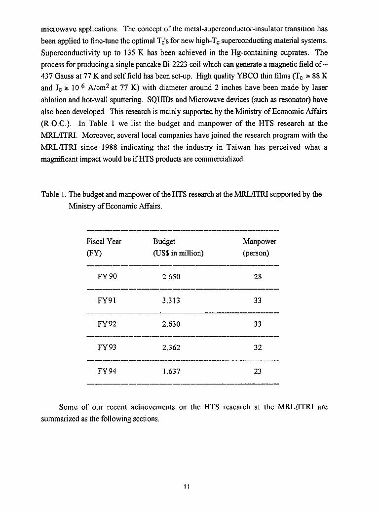
microwave applications. The concept of the metal-superconductor-insulator transition has
been applied to fine-tune the optimalTc's for new high-Tcsuperconducting material systems.
Superconductivity up to 135 K has been achieved in the Hg-containing cuprates. The
process for producing a single pancake Bi-2223 coil which can generate a magnetic field of-
437 Gauss at 77 K and self field has been set-up. High quality YBCO thin films (To _"88 K
and Jc _"10 6 A/cm2 at 77 K) with diameter around 2 inches have been made by laser
ablation and hot-wall sputtering. SQUIDs and Microwave devices (such as resonator) have
also been developed. This research is mainly supportedby the Ministry of Economic Affairs
(R.O.C.). In Table 1 we list the budget and manpower of the HTS research at the
MRL/ITRI. Moreover, several local companies have joined the research program with the
MRLIITRI since 1988 indicating that the industry in Taiwan has perceived what a
magnificant impact would be ifHTS products are commercialized.
Table1.Thebudgetandmanpowerof theHTSresearchat theMRL/ITRIsupportedby theMinistryof EconomicAffairs.
FiscalYear Budget Manpower
(FY) (US$ in million) (person)
FY 90 2.650 28
FY91 3.313 33
FY92 2.630 33
FY93 2.362 32
FY 94 1.637 23
Some of our recent achievements on the HTS research at the MRL/!TRI are
summarizedasthe followingsections.
11
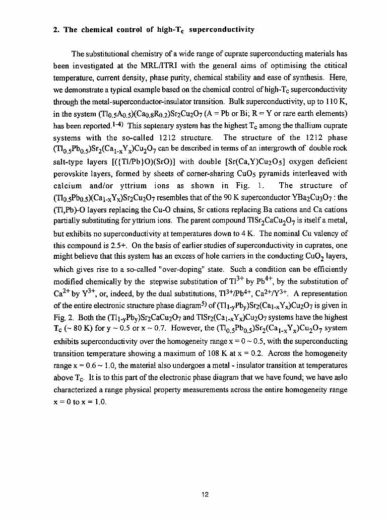
2. The chemical control of high-Tc superconductivity
The substitutional chemistry of a wide range of cuprate superconducting materials has
been investigated at the MRL!!TRI with the general aims of optimising the ctitical
temperature, current density, phase purity, chemical stability and ease of synthesis. Here,
we demonstratea typical examplebased on the chemical controlof high-Tcsuperconductivity
through the metal-superconductor-insulatortransition. Bulk superconductivity, up to 110K,
in the system (Tlo.sAo.5)(Cao.8Ro.2)Sr2Cu207(A= Pb or Bi; R = Y or rare earth elements)
has been reported.1-4) This septenary system has the highest Tc among the thallium cuprate
systems with the so-called 1212 structure. The structure of the 1212 phase
(Tlo.5Pbo.5)Sr2(Cal_xYx)Cu207can be described in terms of an intergrowth of double rock
salt-type layers [({T1/Pb}O)(SrO)] with double [Sr(Ca,Y)Cu2Os] oxygen deficient
perovskite layers, formed by sheets of coruer-sharing CuO5 pyramids interleaved with
calcium and/or yttrium ions as shown in Fig. 1. The structure of
(Tlo.sPbo.5)(Cal-xYx)Sr2Cu207resemblesthat of the 90 K superconductorYna2Cu307 : the
(T1,Pb)-Olayers replacing the Cu-O chains, Sr cations replacing Ba cations and Ca cations
partially substituting for yttrium ions. The parent compoundT1Sr2CaCu207is itself a metal,
but exhibits no superconductivity at temperatures down to 4 K. The nominal Cu valency of
this compound is 2.5+. On the basis of earlier studies of superconductivity in cuprates, one
might believe that this system has an excess of hole carriers in the conducting CuO2 layers,
which gives rise to a so-called "over-doping" state. Such a condition can be efficiently
modified chemically by the stepwise substitution of TI3+by Pb4+, by the substitution of
Ca2+by y3+, or, indeed, by the dual substitutions, TI3+/pb4+,Ca2+!Y3+. A representation
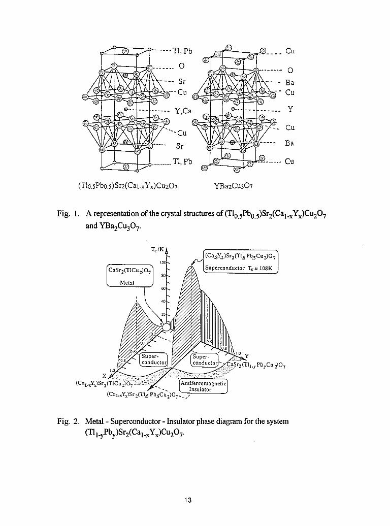
of the entire electronic structure phase diagram5)of (Tll.yPby)Sr2(Cal-xYx)Cu207is given in
Fig. 2. Both the (Tll.yPby)Sr2CaCu207and TISr2(Cal.xYx)Cu207systems have the highestTc (- 80 K) for y - 0.5 or x - 0.7. However, the (Tlo.sPbo.5)Sr2(Cal_xYx)Cu207 system
exhibits superconductivity over the homogeneityrangex = 0 - 0.5, with the superconducting
transition temperature showing a maximum of 108 K at x = 0.2. Across the homogeneity
range x = 0.6 - 1.0,the material also undergoes a metal - insulator transition at temperatures
above To. It is to this part of the electronic phase diagram that we have found; we have aslo
characterized a range physical property measurements across the entire homogeneity rangex=0tox = 1.0.
12
'....... T1,Pb _ __.... Cu
O a
- _ii OSr _ BaCu Cu
Y,Ca_ _[ CuY
"'"Cu
Sr ,: Ba
TI, Pb Cu
(TIo.5Pbo.5)Sr2(Cal-xYx)CU207 "_73a2Cu307
Fig. 1. A representation of the crystal structuresof(Tlo.5Pbo.5)Sr2(Cal.xYx)Cu207
and YBa2Cu307.
Te/K
2(TI.5PbsCu.7)O7]Superconductor Tc = 108K
Y
I.c (TIl.y PbyCu 2_O7X
(Cal.xYx)Sr2(TICu 2)O
(Cal-xY_)Sr 2(TI.5 Pb.sCu
Fig. 2. Metal - Superconductor- Insulatorphase diagram for the system
(T11.yPby)Sr2(Cal_xYx)Cu207.
13
(2) Fabrication of Bi-2223 tapes and their applications in magnets and motors
Ag-clad tapes with the (Bi,Pb)2Sr2Ca2Cu3Olo (hereafter referred to as Bi-2223)
composition were prepared by the PIT (powder-in-tube) technique. Calcined powders were
prepared by coprecipitation method.6) The metal nitrate salts of Bi(NO3)3-5H20, Pb(NO3)2,
Sr(NO3)2, Ca(NO3)2°4H20 and Cu(NO3)2.3H20 were weighted in the mole ratio
1.7L0.4L1.8/2.2/3.2respectively, and dissolved in ethylene glycol with nitric acid finally. The
mixture of the metal nitrate solution was added to the H2C204/Et3N solution with virgorous
stirring. During the coprecipitation process, the pH value of the solution was controlled to
1.5+_0.2by the addition of Et3N. The precitant of the pale blue powder was filtered and then
dried at 120 °C. The dehydrated powders were then calcined at 800 oC, each particle contains
Bi, Pb, Sr, Ca, Cu in appropriate ratios of cation stoichiometry. The calcined powder with the
mainly (Bi,Pb)2Sr2CaCu208 (Bi-2212) phase was then packed into a silver tube, with 12 mm in
outer diameter and 10 mm in inner diameter.The composite was then drawn to about 1.0-1.5mm
in outer diameter in a 15% of area reduction per pass. Multifilamentary wires were prepared by
feeding the drawn mono-core wires to a silver tube, and repeated the above drawing process.
After drawing, the wire was cold rolled into a tape with thinkness about 0.15 mm. The rolled
tape was then sintered at 835-840 °C for 25 - 50 h in air. After first sintering, the sintered tape
was re-rolled into the thinner tape with thickness and width of 0.12 mm and 4 mm, respectively.
Pancake coils were fabricated from these re-rolled tapes. Four monocore tapes were co-wound
in parallel with insulation (used to separate each tum) to form a coil. Inorganic adhesive (alumina
paste) was used as insulator and binder. The coil was then annealed at about 830 °Cfor 50-70 hin air and slow cooled to room temperture in order to transfer the Bi-2212 phase into the Bi-2223
phase.7,8) Transport critical currents were determined by the dc four-probe technique with a
criterion of 1 lxV!cm. A hall effect magnetometer (Oxford model 5200) was used to determine
the central magnetic field (Bo)generatedby pancake coilsat 77 K.
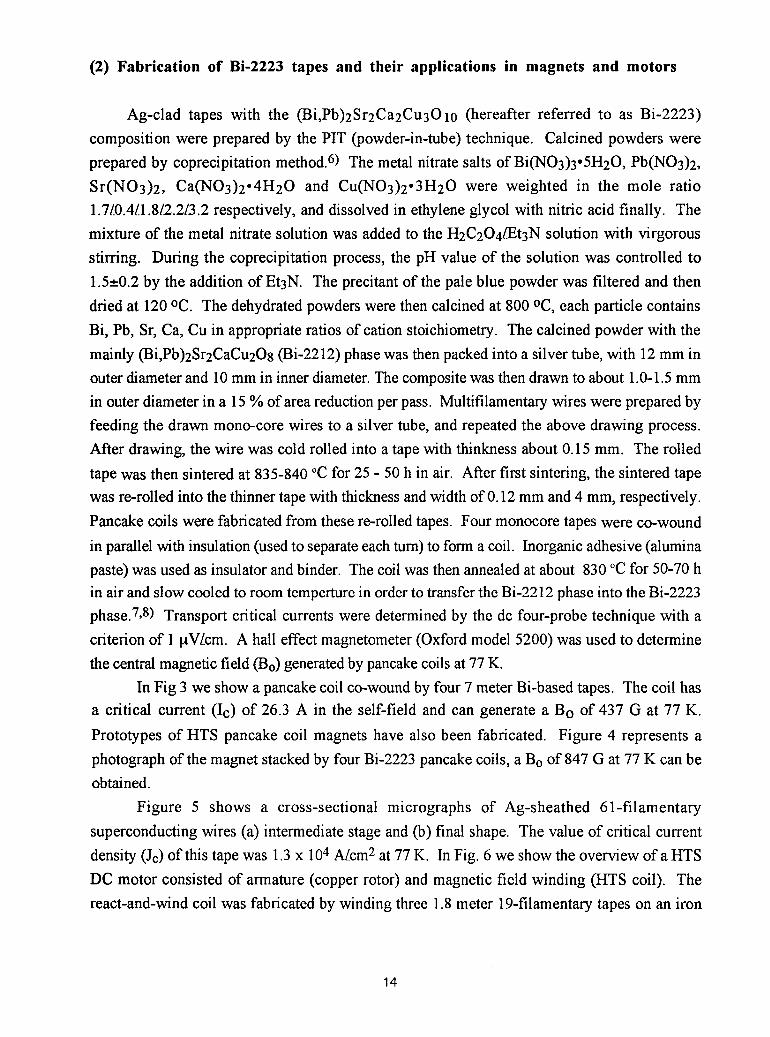
In Fig 3 we show a pancake coil co-wound by four 7 meter Bi-based tapes. The coil has
a critical current (Ic) of 26.3 A in the self-field and can generate a Bo of 437 G at 77 K.
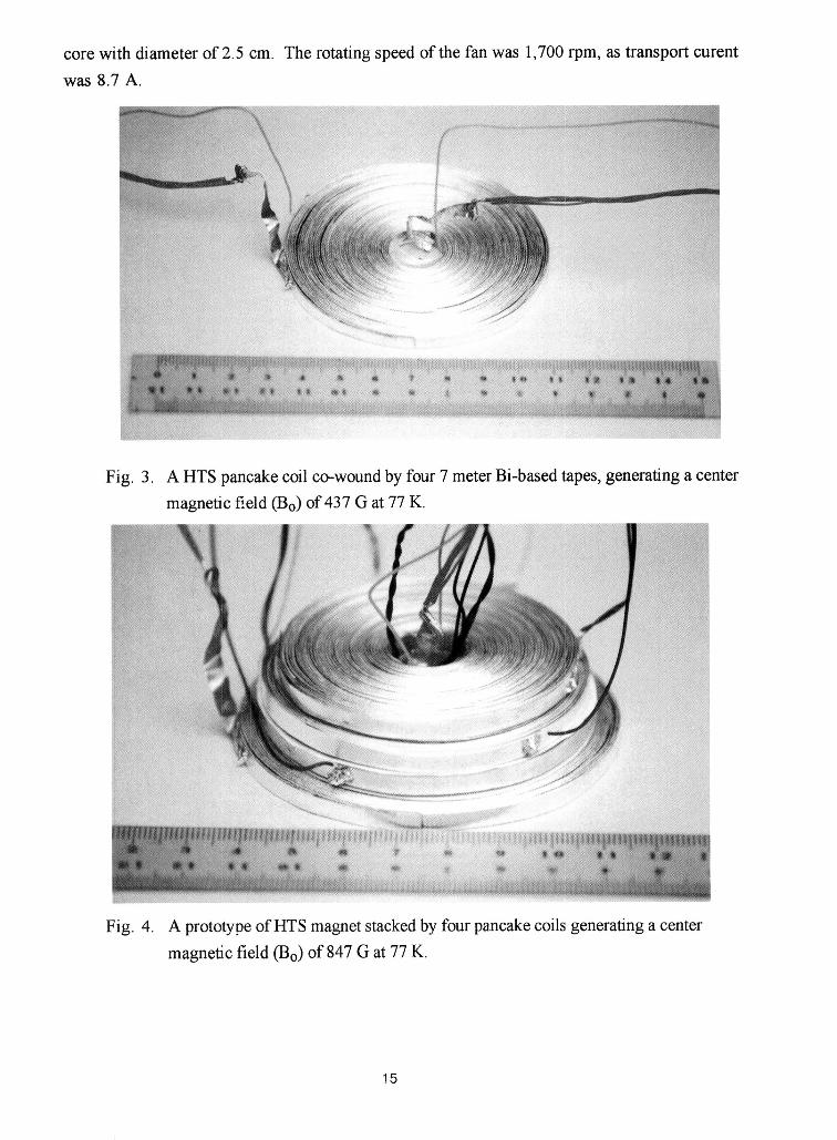
Prototypes of HTS pancake coil magnets have also been fabricated. Figure 4 represents a
photograph of the magnet stacked by four Bi-2223 pancake coils, a Bo of 847 G at 77 K can beobtained.
Figure 5 shows a cross-sectional micrographs of Ag-sheathed 61-filamentary
superconducting wires (a) intermediate stage and (b) final shape. The value of critical current
density (Jc) of this tape was 1.3 x 10⁴A/cm2 at 77 K. In Fig. 6 we show the overview ofa HTS
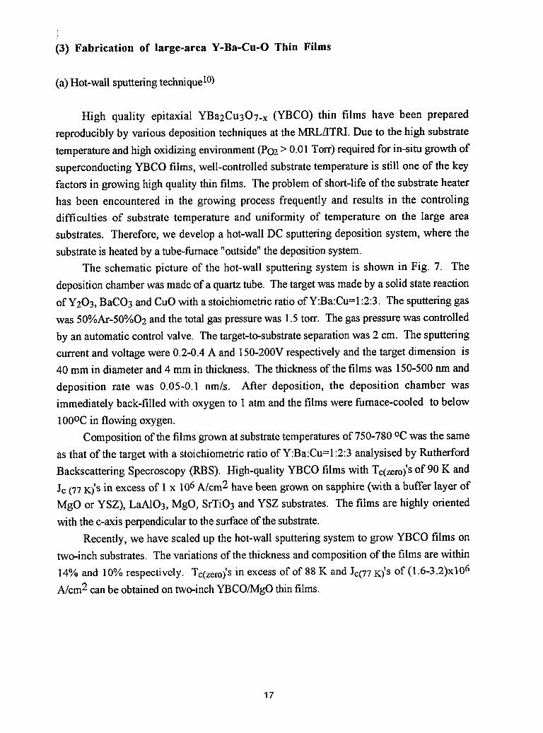
DC motor consisted of armature (copper rotor) and magnetic field winding (HTS coil). The
react-and-wind coil was fabricated by winding three 1.8 meter 19-filamentary tapes on an iron
14
core with diameter of 2.5 cm. The rotating speed of the fan was 1,700 rpm, as transport curent
was 8.7 A.
Fig. 3. A HTS pancake coil co-woundby four 7 meter Bi-based tapes, generating a center
magnetic field (Bo) of 437 G at 77 K.
Fig. 4. A prototypeofHTSmagnetstackedby fourpancakecoilsgeneralanga centermagneticfield(Bo)of 847Gat 77K.
15
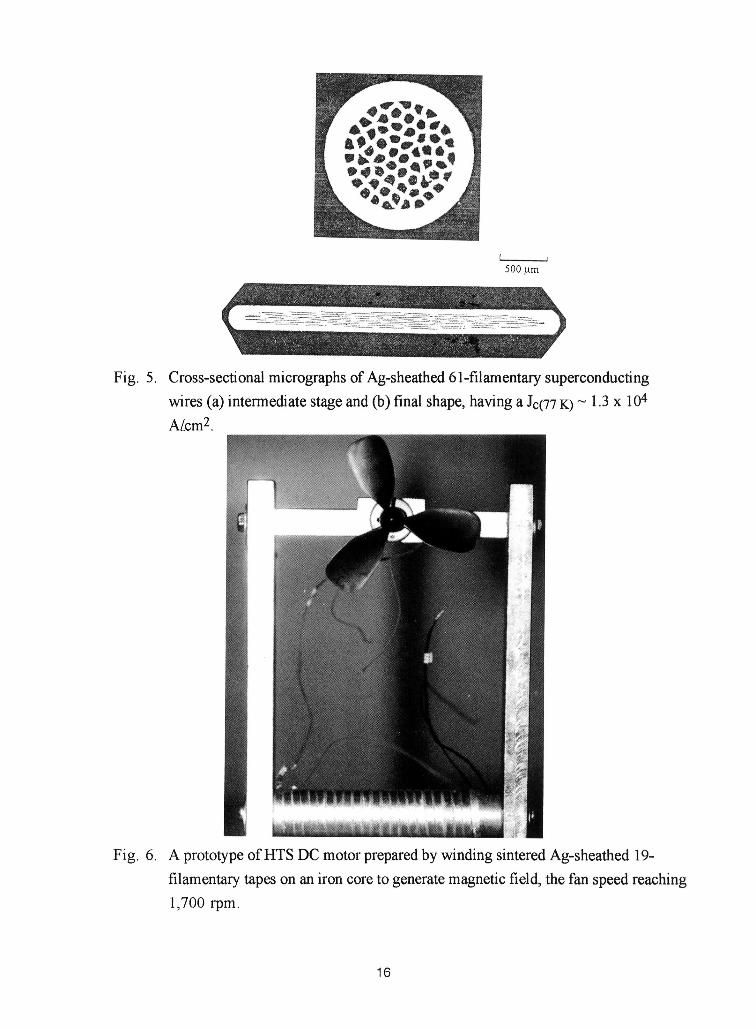
Fig. 5. Cross-sectionalmicrographsof Ag-sheathed61-filamentary superconducting
wires (a) intermediate stage and (b) final shape, having a Jc(77K)_ 1.3x 10⁴AZ.cm2.
Fig. 6. A prototype ofHTS DC motor preparedby winding sintered Ag-sheathed 19-
filamentary tapes on an iron core to generatemagnetic field, the fan speed reaching
1,700 rpm.
16
)
(3) Fabrication of large-area Y-Ba-Cu-O Thin Films
(a) Hot-wall sputteringtechniquO°)
High quality epitaxial YBa2Cu307-x (YBCO) thin films have been prepared
reproducibly by various deposition techniques at the MRL/ITRI. Due to the high substrate
temperature and high oxidizing environment (Po2> 0.01 Torr) required for in-situ growth of
superconducting YBCO films, well-controlled substrate temperature is still one of the key
factors in growing high quality thin films. The problem of short-life of the substrate heater
has been encountered in the growing process frequently and results in the controling
difficulties of substrate temperature and uniformity of temperature on the large area
substrates. Therefore, we develop a hot-wall DC sputtering deposition system, where the
substrate is heated by a tube-furnace "outside" the depositionsystem.
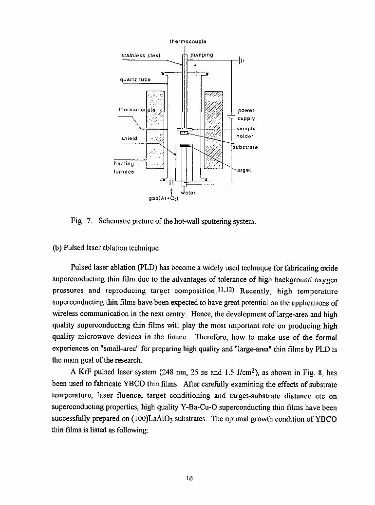
The schematic picture of the hot-wall sputtering system is shown in Fig. 7. The
deposition chamber was made of a quartz tube. Thetarget was made by a solid state reaction
of Y203, BaCO3 and CuO with a stoichiometric ratio ofY:Ba:Cu=1:2:3. The sputtering gas
was 50%Ar-50%O2 and the total gas pressure was 1.5ton'. The gas pressure was controlled
by an automatic control valve. The target-to-substrate separation was 2 cm. The sputtering
current and voltage were 0.2-0.4 A and 150-200V respectively and the target dimension is40 mm in diameter and 4 mm in thickness. The thickness of the films was 150-500 nm and
deposition rate was 0.05-0.1 nm/s. After deposition, the deposition chamber was
immediately back-filled with oxygen to 1 atm and the films were furnace-cooled to below
100oc in flowing oxygen.
Composition of the films grown at substrate temperatures of 750-780 °C was the same
as that of the target with a stoichiometric ratio of Y:Ba:Cu=1:2:3 analysised by Rutherford
Backscattering Specroscopy (RBS). High-quality YBCO films with Tc(zero)'Sof 90 K and
Jc (77K)'Sin excess of 1 x 10⁶A/cm2 have been grown on sapphire (with a buffer layer of
MgO or YSZ), LaAIO3, MgO, SrTi03 and YSZ substrates. The films are highly oriented
with the c-axis perpendicular to the surface of the substrate.
Recently, we have scaled up the hot-wall sputtering system to grow YBCO films on
two-inch substrates. The variations of the thickness and composition &the films are within
14% and 10% respectively. Tc(zero)'Sin excess of of 88 K and Jc(77K)'s of (1.6-3.2)x106A/cm2 canbe obtained on two-inchYBCO/MgOthin films.
17
thermocouple
stainlesssfeel _-_ p lmping, ,1,"" I J
thermocot p ,./ ,,;_; _ power
--'x _'""""'I 1> r-_ 'Y""::_";:" supply•.,:,". ,, -.;,.,,/.
shield .,.:._ ,..
".;_i"::":: ubstrate
heatingfurnace "target
tgaslAr+O21
Fig. 7. Schematic picture of the hot-wall sputteringsystem.
(b) Pulsed laser ablation technique
Pulsed laser ablation (PLD) has become a widely used technique for fabricating oxide
superconducting thin film due to the advantages of tolerance of high background oxygen
pressures and reproducing target composition.ll, 12) Recently, high temperature
superconducting thin films have been expected to have great potential on the applications of
wireless communication in the next centry. Hence, the development of large-area and high
quality superconducting thin films will play the most important role on producing high
quality microwave devices in the future. Therefore, how to make use of the formal
experiences on "small-area" for preparing high quality and "large-area"thin films by PLD is
the main goal of the research.
A KrF pulsed laser system (248 nm, 25 ns and 1.5 JLcm2),as shown in Fig. 8, has
been used to fabricate YBCO thin films. After carefully examining the effects of substrate
temperature, laser fluence, target conditioning and target-substrate distance etc on
superconducting properties, high quality Y-Ba-Cu-O superconducting thin films have been
successfully prepared on (100)LaAIO3substrates. The optimal growth condition of YBCO
thin films is listed as following:
18
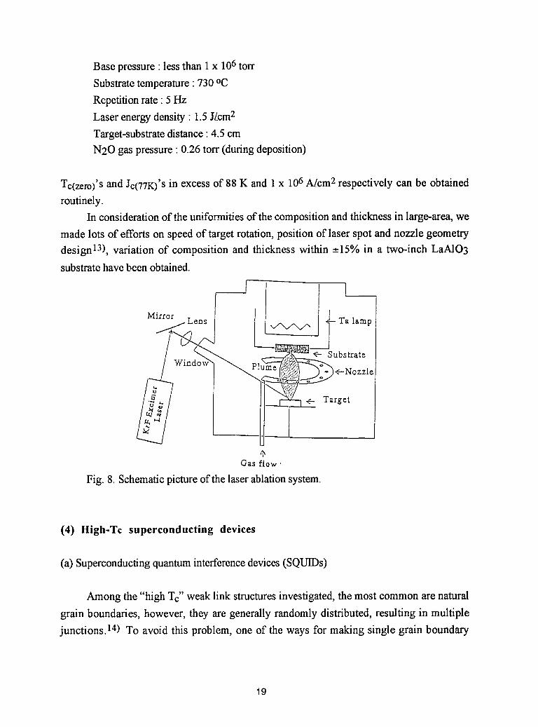
Base pressure :less than 1 x 10⁶torr
Substrate temperature: 730 °C
Repetitionrate : 5 Hz
Laser energy density : 1.5J/cm2
Target-substratedistance : 4.5 cm
N20 gas pressure : 0.26 torr (during deposition)
Tc(zero)'Sand Jc(77K)'S in excess of 88 K and 1 x 10⁶A!cm2 respectively can be obtained
routinely.
In consideration offlae unifo..rmitiesof the composition and thickness in large-area, we
made lots of efforts on speed of target rotation, position of laser spot and nozzle geometry
designl3), variation of composition and thickness within __.15%in a two-inch LaA103substrate have been obtained.
Mirror Ta lamp
Target
,bGas flow"
Fig. 8. Schematic picture of the laser ablation system.
(4) High-Tc superconducting devices
(a) Superconducting quantum interferencedevices(SQUIDs)
Among the "high T "c weak link structures investigated, the most common are natural
grain boundaries, however, they are generally randomly distributed, resulting in multiple
junctions. 14) To avoid this problem, one of the ways for making single grain boundary
19
junctions, epitaxial films deposited on bicrystal substrate, has been suggested and shows
some optimistic results on sensitivity and noise-reduction.15,16)
We have also successfully developed the fabricationtechnologies of DC-SQUIDs with
highly reproducibility.17,18) The TI2Ba2Ca2Cu3Olo(TI-2223) DC-SQUIDs, patterned by
standard photolithography techniques, show modulationdepth (peakto peak) up to 90_tV,as
shown in Fig. 9. After the successful development of the bi-epitaxial grain boundary
Josephson junction at the MRL/ITRI. YBCO bi-crystal DC-SQUIDs with magnetic field
modulation in excess of 1_V can be obtained, as shown in Fig. 10.
;>:_- lOO
"_'--"__"_,,.,__"€_e_____, 742248-4 _ Ibl"=0"25mA_-30 _ ' _
0.00 0.10 0.20 0.30 0.40 0.50
Magnetic field (Oe)
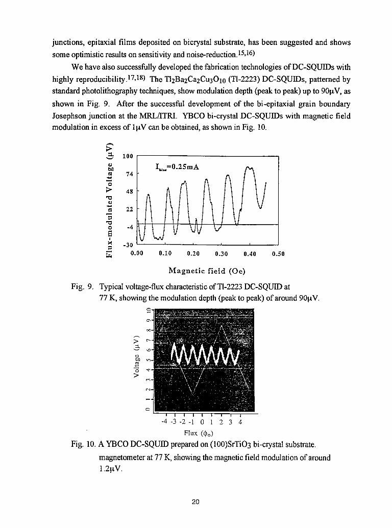
Fig. 9. Typical voltage-fluxcharacteristicofT1-2223De-SQUID at77 K, showing the modulation depth (peak to peak) of around 90_V.
o
! 1
-4 -3 -2-1 0 1 2 3 4
Flux(_o)Fig. 10.A YBCO DC-SQUID preparedon (100)SrTiO3bi-crystal substrate.
magnetometerat 77 K, showing the magneticfield modulation of around1.2.uV.
2O
(b)High-Tcsuperconductingresonators
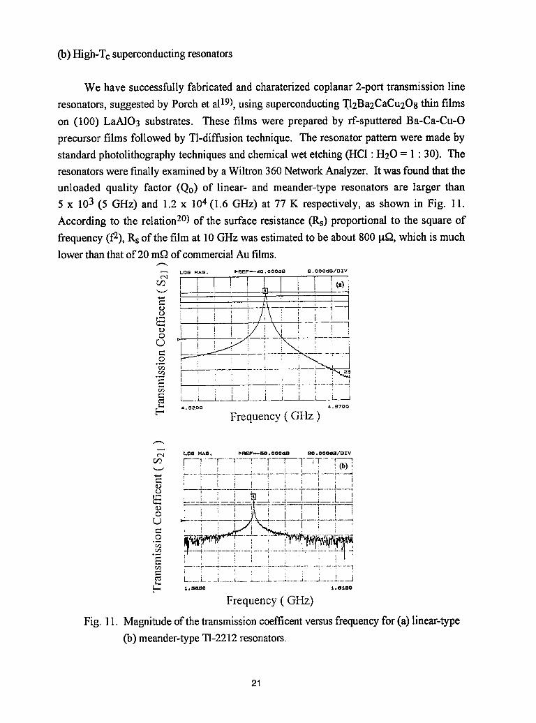
We have successfully fabricated and charaterized coplanar 2-port transmission line
resonators, suggested by Porch et a119),using superconducting T12Ba2CaCu208thin films
on (100) LaAIO3 substrates. These films were prepared by rf-sputtered Ba-Ca-Cu-O
precursor films followed by Tl-diffusion technique. The resonator pattern were made by
standard photolithography techniques and chemical wet etching (HCI : H20 = 1 : 30). The
resonators were finally examinedby a Wiltron 360 Network Analyzer. It was found that the
unloaded quality factor (Qo) of linear- and meander-type resonators are larger than
5 x 10³ (5 GHz) and 1.2 x 10⁴(1.6 GHz) at 77 K respectively, as shown in Fig. 11.
According to the relation2°) of the surface resistance (its) proportional to the square of
frequency (f2), Its of the film at 10 GHz was estimated to be about 800 lXff_,which is muchlower than that of 20 mQ of commercialAu films.
LOG HAG. _REF_40. O00c:IB 8. O00dB/OZV
"_" - I]
- . .....
E i ;-----__ i I i I i : 1L L_.i_L____._j iI--i ,4. 9200 4. 9700
k-, Frequency ( GHz )
LO_i It_.li, I_l___g_150 oO00cllS RO. O00118/'DZV......... ---"r ...... -m--- ..... r--
I ; I i ! i , I i+-
' ' f ! i i I! , i , a , _ , i
r) *"---,-F--'-_---_-- " ."'--T-----'---T---'T--
_ __L._ ,, ,-m--'--....... : -----.-'.' .....
"_= i' i i ! i ; : i ! i I_- --....__.... -____L......_...... L_...._L____.....4 ..... ;..... 7t_ i ; ' , . i : ! i .
L ..... L.... t ....... t__ .___,..x___A__..] ..... j___A__ ._J
l..III150 _.,III.II0
Frequency(GHz)
Fig. 11. Magnitude of the transmissioncoefficent versusfrequency for (a) linear-type
(b) meander-type TI-2212resonators.
21
Acknowledgem ents
The authors would like to thank the Ministry of Economic affairs for the financial
support of the HTS research at the MRLflTRI. We also wish to thank Dr. H.C. Lei,
Dr. K. Chen, Mr. R. J. Lin and Dr. C. J. Huang for the help to organise this manuscript.
References
1) R.S. Liu, J. M. Liang, S. F. Wu, Y. T. Huang, P. T. Wu and L. J. Chen, Physica C
159, 385 (1989).
2) P.T. Wu, R. S. Liu, J. M. Liang, Y. T. Huang, S. F. Wu and L. J. Chen,
Appl. Phys. Lett. 54, 2464 (1989).
3) J.M. Liang, R. S. Liu, Y. T. Huang, S. F. Wu, P. T. Wu and L. J. Chen, Physica C
165, 347 (1990).
4) Y.T. Huang, R. S. Liu, W. N. Wang and P. T. Wu, Jpn. J. Appl. Phys. 28, L1514
(1989).
5) R.S. Liu, P. P. Edwards, Y. T. Huang, S. F. Wu and P. T. Wu, J. Solid State Chem.
86, 334 (1990).
6) D.S. Shy, W. H. Lee, and R. S. Liu, Proceedngs of the 1994 Annual Conference of the
Chinese Society for Materials Science 1, 290 (1994).
7) Y.T. Huang, S. F. Wu, and D. S. Shy, Proceedngs of the 1994 Annual Conference of the
Chinese Society for Materials Science 1, 332 (1994).
8) K. Chen, L. Homg, H. S. Koo, C. Y. Shei, L. P. Wang, C. Chiang, T. J. Yang,
W. H. Lee, and P. T. Wu, Appl. Phys. Lett. 59, 1635 (1991).
9) K. Chen, L. Hormg, C. H. Tai, J. C. Wei, T. J. Yang, and J. T. Lue, Chinese J. Phys.31, 1049 (1993).
10) R. J. Lin and L. J. Chen, Appl. Phys. Lett. 62, 105 (1993).
11) D. Dijkkamp, T. Venkatesan, X. D. Wu, S.A. Shaheen,N. Jisrawi, Y. H. Min-Lee,
W. L. Mclean and M. Croft, Appl. Phys. Lett. 51, 619 (1987).
12) M. C. Foote, B. B. Jones, B. D. Hunt, J. B. Barner, R. P. Vasquez and L. J. Bajuk,
Physica C 201, 176 (1992).
13) C. M. Chang, H. C. Lai and R. J. Lin, Proceedngs of the 1994 Annual Conference of the
Chinese Society for Materials Science 1, 328 (1994).
22
14) B. Oh, R. H. Koch, W. J. Gallagher, V. Foglietti, G. Koren, A. Gupta, and W. Y.
Lee, Appl. Phys. Lett. 56, 2575 (1990).
15) D. Dimos, P. Chaudhari J. Mannhart, and F. K. LeGoues, Phys. Rev. Lett. 61, 219
(1988).
16) R. Gross, P. Chaudhari, M. Kawasaki, m. B. Ketchen, and A. Gupta, Appl. Phys.
Lett. 57, 727 (1990).
17) T. L. Chen, S. F. Wu, Y.C. Chen and R. J. Lin, Proceedngs of the 1993 Annual
Conference of the Chinese Societyfor Materials Science, 7-5 (1993).
18) Y. C. Chen, T. L. Chen, R. J. Lin, and S. F. Wu, Chinese Journal of Physics 31,
1109 (1993).
19) A. Porch, M. J. Lancaster, R. G. Humphreys and N. G. Chew, Presented at Applied
Superconductivity Conference, Chicago, Aug. 23-28, 1992.
20) M.R. Namordi, A. Mogoro--Campero,L. G. Turner and D. W. Hogue, IEEE Trans.
Microwave Theory Tech. 39,1468 (1991).
23
PROGRESS IN SUPERCONDUCTIVITY:THE INDIAN SCENARIO
Manu MultaniTata Institute of Fundamental Research, Bombay 400 005, India
V.K. MishraDepartment of Science & Technology, Government of India, New Delhi 110 012, India
India has made rapid progress in the field of high temperature superconductivity,beginning at the time of publication of the Zeitschriflfi_r Physik paper by Bednorz and Mfiller.Phase I of the program was conceived by the Department of Science & Technology of theGovernment of India. It consisted of 42 projects in the area of basic research, 23 projects inapplications and 4 short-term demonstration studies. The second phase started in October 1991and will run through March 1995. It consists of 50 basic research programs and 24 applicationprograms. The total investment, mainly consisting of infrastructural development to supplementexisting facilities and hiring younger people, has amounted to about Indian Rupees 40 crores,equivalent to about US$ 13 million. The expenditure for the period 1992-1997 shall be uptoabout Rs. 27 crores, equivalent to about US$ 9 million. The basic idea is to keep pace withdevelopments around the world.
It is noteworthy to remark that during the above-mentioned period several books havebeen published. Some of the titles are: ChemicalAspects of High Temperature Superconductivity,edited by C.N.R. Rao (World Scientific Publishing Company, Singapore, 1991),Superconductivity Today, C.N.R. Rao and T.V. Ramakrishnan (Wiley Eastern, 1992), Proc. ofthe International Conference on Superconductivity, edited by S.K. Joshi, C.N.R. Rao and S.V.Subramanyam, a Series (now in its 13th. volume) entitled Studies in High TemperatureSuperconductors, edited by A.V. Narlikar, Thallium-Based High Temperature Superconductors,edited by J.V. Yakhmi and A.M. Hermann (Marcel-Dekker, New York, 1994), Selected Topicsin Superconductivity - A Flavor of Current Trends, edited by L.C. Gupta and M.S. Multani (aspart of a nine-volume series on Frontiers in Solid State Sciences, World Scientific PublishingCompany, 1993-1995), Physical and Material Properties of High Temperature Superconductors,edited by S.K. Malik and S.S. Shah (Nova Science Publishers, Inc., New York, 1992),Theoretical and Experimental Approaches to High Temperature and ConventionalSuperconductors, edited by L.C. Gupta (Nova Science Publishers, New York, 1991)
One of the highlights of our achievements is the discovery of borocarbides assuperconductors. Prof. R. Nagarajan, the main discoverer of this new family, is giving aseparate talk on this. So I shall not dwell on it. We shall outline below the main achievementsof the past two to three years.
24
SYNTHESIS AND CHARACTERIZATION
Thin Films
The growth of high quality high-Tc superconductor films on semiconductor substratesis an important step towards the possible marriage of two technologies. A recent study by thePoona University group was the realization of Y-123/YSZ epitaxial configuration on Si (100)by pulsed laser ablation without the chemical removal of the native surface oxide. Thecrystalline characteristics of the deposited films have been studied by x-ray diffraction (XRD),high resolution transmission electron microscopy (HREM) and Rutherford backscattering(RBS) techniques. Typically, the superconducting films of thickness 500 nm deposited on siliconwith 150 nm epitaxial Y-ZrO 2 buffer layer have Tc as high as 88 K and Jc of 2x10⁵ A/cm 2at77 K for a 5 I.tm bridge pattern (using the same KrF excimer laser as for pulsed laserdeposition). 1
The group has deposited superconducting thin films as well as buffer layers using theKrF excimer laser (_. = 248 nm). The substrates include Y-ZrO2 , LaA103 , LiNbO3 ,Gd3GasO12and Si (100).Detailed studies addressingsuch issuesas epitaxy,interface reactions,grain structure and coupling have been carried out. Effects such as those of dopants, devicesand other physical properties will be described later in this talk in the relevant sections. Thecharacterization was done at the laboratory of one of the authors (MM).2 A group at theBhabha Atomic Research Center (BARC, Bombay)has been growingsingle crystalsubstrates.
Granularity of HTSC (bulk as well as thin) materials is a characteristic disadvantage ofthe laffered superconductors. While one single crystal grain of an HTSC film can support a Jc> 10' A/cm 2 at 77 K, most bulk materials measurements show 3 to 4 orders of lower criticalcurrent density. Thin epitaxial films have improved these values considerably - but not quiteclose to the intrinsic value of a single crystal. A group at the Tata Institute of FundamentalResearch has prepared Ag-doped (5 wt.%) and undoped Y-123 films by PLD. 3 The excimerlaser fluence was 3 J/cm 2 The growth of the film was carried out at 200 mTorr oxygen, atarget-substrate distance of 5 cm and a laser repetition rate of 10 Hz. A normal oxygen coolin 500 Torr oxygen was provided as post deposition oxygenation. The group found that Ag-doping considerably improves the microstructure, leading to larger and well-aligned grains withnarrower grain boundaries. A 10 I-tmwide rnicrobridge led to a J_ = 1.4x10⁷A/cm 2 at 77 K on(100) SrTiO 3. Implications of this for devices is discussed in the appropriate section.
Innovative design and development for producing in situ superconducting thin films andmake property-structure-deposition parameter correlations have been made by a group at theIndian Institute of Science (I.I.Sc., Bangalore). A technique with the acronym HOST (Highpressure oxygen sputtering technique) was developed and in situ superconducting Y-123 filmshave been successfully prepared. To prove the superiority of HOST over the conventionalsputtering techniques, detailed investigations have been carried out on HOST plasma bystudying the I-V characteristics and by carrying out Langmuir probe studies and opticalemission spectrometry (OES). These studies have revealed that in high pressure oxygen plasmaat elevated substrate temperatures, negative oxygen ion energy was extremely small and thenumber of ions near the substrate were also small. This clearly explains why the negativeoxygen ions cannot disturb the composition of the films in HOST. It was also observed that the
25
positive ion population was more in this technique and, hence, deposition rates were high.
Y-123 films have been deposited on MgO, SrTiO3, and I_xA103by HOST. Auger andRBS channeling studies have indicated that the filmsare stoichiometric and perfectly oriented.The films were uniform (better than 1 percent) over an area of I cm.z . The challenging taskof depositing large-area (60 mm or more) films has begun with the design of Facing TargetSputtering (FTS). Investigations have been carried out to study the effect of target diameter,target-substrate distance, operating pressure, inter target distance,I-Vcharacteristics, Langmuirprobe studies, negative bias voltage on the substrate, and a variety of other parameters arebeing studied for optimal deposition rate and quality.
A significant aspect of the research by another group at the I.I.Sc. has been thesynthesis,purification and characterization of all the organometallic precursors needed for theCVD process. Initially,dipiraoxylmethanates(DPM) of Y, Ba and Cu were synthesized.Thesehave been used by other investigatorsas well.More recently, a new 13-diketonateprecursor hasbeen synthesizedfor each metals. These precursors, the keto-carboxylates,have been found tobe very useful and, perhaps, better than the DPM precursors. The processes for the synthesisand purification of the various precursors have been scaledup to yield usefullylarge (10 grams)quantities. Due to polymerization-relatedproblems with Ba precursors, onlypoor quality high-Tchave been obtained so far by MOCVD.
A group at the National PhysicalLaboratory ( NPL, NewDelhi) has achieved very goodepitaxial films of the Y-123 system by the technique of dc magnetron sputtering. These filmshave been grown in situ on the followingsubstrates: SrTiO3(100), LaA103(100), MgO (100),YSZ (100) and the r-plane of sapphire.4The sputtering gas consisted of a flowingmixture ofargon and oxygen (in the ratio 2:1) at pressures varying between 200 to 1600 mTorr. Theeffects of sputtering gas pressure and the substrate temperature in the on-axis geometry (30mm distance) were characterized by XRD, SEM, RBS, VSM, R-T and Xac-T.
The value of the critical current has been estimated as a function of the magnetic fieldusing Bean's modified critical state model. The typicalvalues of Jc at zero field and 12 kOeare 2.2x10 7 and 1.6x10⁶ A/cm2"at 77 K
Fullerenes and Related SystemsThe Indira Gandhi Center for Atomic Research (IGCAR, Kalpakkam) group has
synthesizedC60and C70along with the alkali dopants, K and Rb. Somepreliminary studies havealso been made on co-doping K with Pb or Bi. The nominal compositions were PbK2C60andBiKzC60were prepared in the vapor phase reaction, starting with the stoichiometricconstituents. XRD and ;_ac-Tmeasurements indicate that while Pb and Bi are incorporated inthefcc lattice, there is no appreciable change in Tcunlike in the case of Tl-doped samples. Ondoping C60samples with Yb it is seen that Yb2C,Yb3C60and Yb6C60 are formed. The observedsuperconductivitybelow 5.4 K is due to the fcc compound with the least Yb.(See ref.5 andcitations therein)
The group of one of the authors (MM) in collaboration with the Poona Universitygrouphas also been looking a Raman scattering from thin filmsof carbon-60 clusterswith admixtures
26
of the carbon-70. The 488 nm Ar. radiation in the backscattered geometry has been used tocharacterize the different bonding types. Diamond films have been the focus of study by thetwogroupswith respect to novelsynthesistechniques. We have achieved formation of diamondfilms by laser-induced reactive quenching at the liquid-solid interface between a suitabilityorganic liquid such as cyclohexane (in view of its stereochemical aspects) and a well-characterized substrate such as tungsten. A nanosecond laser pulse is made incident on a thinlayer of cyclohexane or decalin supported on a tungsten foil. An area of 5 mm x 5 mm isthermally shocked in the scan mode by the laser pulses. The evidence from glancing angleXRD, TEM and laser Raman spectroscopyshow,conclusively,the formation of hexagonal andcubic diamonds on the surface of tungsten. The choice of the organic liquid is found to becrucial.
A second group at NPL has recently published a paper reporting on the observationof imperfect carbon cage structures of C60by high-resolution scanning tunneling microscopy.6The imperfect carbon cages have been resolved to the finest detail, which, for the first time,provide adequate confirmation of a variety of defect structures predicted by moleculardynamics simulations. From the conductance spectra by in the STS mode, one observes thatthe gap between the HOMO and LUMO for the clusters is decreased with the presence ofdefects. From the value of 1.5 eV for the perfect cage, the imperfect cage can lead to gapvalues of 0.3 eV or even lower, perhaps to zero value.
Powders and CompactsA new technique called the pyrophoric process has been developed to synthesize
ultrafine powders of the Y-123 system.The nanoparticles ( 40 nm) and have been observed tosinter to 99% densityby processingthe pellets at much lower temperatures (880 C) and shorterlengths of time (1 hr.) than other processes, viz., the conventional ceramic process or thecoprecipitation technique.
C-axis oriented Y-123 whiskers have been synthesized to fabricate whisker-reinforcedY-123 composite, which show partial c-axis orientation after sintering and a Jcvalue of 1440A/cm 2at 77 K.
In collaboration with the Universityof Florida group, the author's (MM's) group at hasinvented the method of synthesizinghigh density(about 97% of single-crystaldensity) of Y-123ceramics with a large Meissner fraction ( 90% unoptimized). The technique involves the useof microemulsions which has been the focus of many studies reported in the past decade bychemistsas well asphysicists.The microemulsion-derivedpowders sintered with explosivegraingrowth from about 40 nm to about 50x103nm (along the longer axis of the ellipsoids).Thereare ramifications for high Jc in bulk superconductors from these studies.
The IGCAR group has designed a vacuum calcination method for the synthesisof hightemperature superconductors. The essence lies in decomposition of precursors (from the co-precipitation, citrate, or sol-gelroutes) in the quick removal of the CO2whichwould otherwisereact with the Y-123 to form BaCO3, Y203, CuO and Y2Cu2Os,depending on the temperature.The reduced pressure calcination circumvents this by more effective removal of the carbon
27
dioxide. Presently, synthesis of upto 150 grams of Y-123 powder per batch has beenstandardized. The process parameters are wellunderstood and there should be no difficultyinscaling up the process for 500 grams batch size. An annual production upto 100 kg of well-characterized material is well within reach.
A new semi-wet route to the synthesis of Pb-doped Bi-2223 powders free fromcontamination by the 2201 and 2212 stoichiometries has been developed. This process requires48 hours to complete. By following the sequence of the thermochemical reactions, it is shownthat Ca2PbO4 and 2212 formed in the early stages of reaction, in conjunction with CuO, playthe most crucial role in accelerating the formation of the 2223 phase. 7
The Defence Metallurgical Research Laboratory (DMRL, Hyderabad) has synthesizedY-123 powder which leads to sintered compacts with high current densities and levitationproperties using quenched melt growth (QMG) and modified QMG techniques. The group hasalso prepared Y-123 sputtering targets of high quality.
TowardsNew SuperconductorsIt was recently shownthat YSr2Cu307, whichis not otherwisepossible to prepare under
ambient conditions, can be stabilized by the incorporation of oxyanions such as carbonate,sulfate and phosphate. Such oxyanion derivatives of the 123 cuprates are renderedsuperconducting by the partial substitution of Y by Ca, Sr by Ba, or by the substitution ofcarbonate by nitrate. It has been noted that YSr2Cu2.8(POa)0.2Oyis stable in the orthorhombicstructure, but the material is non-superconducting. The group has found that increasing thehole concentration through partial substitution of Y by Ca typically by 30 atomic percentrenders the complex system superconducting (To 40 K). Once again, by incorporating the 0.2phosphate group in the Cu site of orthorhombic YBaSrCu307,a stable tetragonal derivativewith a transition temperature of 47 K has been prepared. The Tc increases to 70 K by 30atomic percent substitution of Y by Ca. The IR spectrum of this system confirms the presenceof the phosphate group in the C2,,symmetry. This observation is significant since no otherstable 123-type cuprate is known to be formed in the Y-Ca-Sr-Cu-O system under theexperimental conditions employed; let alone exhibit superconductivity.
When the Cu(1) site in orthorhombic YBaSrCu307_(Tc = 80 K) is partly substituted bythe carbonate ion (upto 50%), the crystalstructurebecomes tetragonal and electron diffractionpattern shows evidence for 2a x 2c superstructure; the material, however, is notsuperconducting. The same is true when Y is partly replaced by Ca as inYCaBa2Sr2Cus(CO3)Oy.When the CO3 group is partly by the NO 3 group as in theYCaBa2Sr2Cus(CO3)1.x(NO3)xOy,the structure remains the same but superconductivity isretained. The IR spectroscopic studies show that both, CO3and NO 3 coordinate strongly andare not present as free ions in these oxyanioncuprate derivatives.Cu K-EXAFS studies on thecarbonate and carbonato-nitrate derivatives confirm the presence of oxyanions in the placeof CuO4units in the Cu-O chains.
Incorporation of the BO33- stabilizes the YSr2Cu307 but the borate derivative is notsuperconducting. Neither is superconductivity obtained by partial substitution of Y by Ca.Superconductivity appears, however, when Sr is partially replaced by Ba. Now, dramatically,
28
50 atomic percent replacement of Y by Ca remains superconducting. The borate ion iscoordinated to Cu, reducing its point group symmetry.Observation of superconductivityin theborate derivatives prepared under ambient conditions is noteworthy.
The important point to note is that the cuprate familycompounds are, essentially,beingfine-tuned to observe subtle changes in the electronic properties. Such an approach can leadto an identifiable mechanism of the new ceramic superconductivity.It can also lead to higheror well-tailored transition temperatures. The derivative, T10.sPb0_sSraCu2(SO4)Oy,has beensynthesizedwith the same motivation. Infrared spectra show that the sulfate ion is present asa bidentate ligand as expected from the structural space group, P4/mmm. (See refs. 8, 9 andcitations therein)
CoatingsPlasma sprayingof high-Tosuperconductors offers somescope for large scale processing.
The results of work done at Bharat Heavy Electricals Ltd. (BHEL, Hyderabad) are reported.Essentially, in the plasma spray process, feed stock material in the form of powder is injectedinto a high-temperature, high-velocity,plasma stream. The temperatures have been estimatedto be in the region of 4000-12,000K while the velocities may lie in the vicinityof 100-200m/s.These fast-moving molten droplets form a deposit (coating) when they are suddenly stoppedby a relatively cold substrate. We can, therefore, see that the heat and momentum transferfrom the plasma jet to the powder particles are of crucial importance for achieving goodcoatings.The arc current, plasma gas composition and flow,and particle size of the feed stockpowder are the primary parameters which need to be optimized. Substrate distance from thegun nozzle and the substrate temperature are also relevant parameters as they dictate thespeed with which solidificationtakes place on impact and govern porosity and micro cracks inthe deposited coating.
TapesBHEL has also been engaged in the design and development of tapes. Silver-sheathed
tapes were fabricated using the Bi-2223system.The tapes were processed to final thicknessbydirect rolling as well as by repeated rolling with intermediate heat treatment. The rollingreduction rate was also varied to find its effect on the final properties. The critical currentmeasured at 77 K could be enhanced from 2770 A/cm2 for directly roiled tapes to 12,500A/cm 2by repeated rolling under identical conditions. In repeatedly rolled tapes the Jc " Bvariations were found to be much lower in comparison to the directly rolled tapes. Textureevaluation using angular dependence of the magnetoresistance showed the a-b planeorientation to be along the rolling direction..
The powder-in-tube technique using an Ag sheath has emerged as the only viablemethod for fabricating long lengths of flexibleHTSC tapes. The Bi:Pb ratio in the above 2223system was 1.8 : 0.4. The average particle size of the powder was about 2 I.tm.The BHELgroup has now completed angular magnetoresistance (AMR) studies to garner usefulinformation regarding the texture in the tape described above.The magnetic field is providedby suitably chosen gap distance between two NdFeB permanent magnets. The gap is adjustedso that the uniform field is more than Hcl of the Bi-2223 system (where Bi is partially
29
substituted by Pb). The fixture for changing the field direction is such as to change the angle(0) between the transport current (in the plane of the tape) direction and the applied magneticfield direction. The range covered is 0_0_180. The BHEL group has completed a study alongwith the Argonne National Laboratory and the Regional Research Laboratory (Trivandrum)on the influence of initial composition and processing parameters on the critical current densityof BPSCCO PIT process tapes.
TOWARDS DEVICES
The etch kinetics of Y-123 films have been investigated for fabrication of 2 I_mwidthmicrobridges by photolithography. The films have been etched to form different patterns ofmicron dimensions. It has been shown that Y-123 could be patterned down to microndimensions by controlled wet etching using EDTA as an etchant and by lift-off technique. Lift-off technique requires fewer number of processing steps and avoids exposure to chemicaletchants. EDTA is an admirably suitable etchant. The critical current density has been foundto increase with decreasing linewidthswhich is due to decreasing number of weak links in theactive microbridge area.
The same group at the Indian Institute of Technology (IIT, Kharagpur) has now beenable to grow 5 monolayer thick 2201 and 2212 phases of BSCCO either singlyor one on topof the other by the atomic layer deposition (ALD) process. In this method, the group hassequentially evaporated Bi and Cu from K-cells and SrO and CaO from e-beam guns ontoMgO (100) substrates heated to 700 C. During the deposition, oxygen gas containing 10%atomic oxygen(generated by dc. discharge inside a U-shaped tube with a very fine hole in thebent portion which allows the atomized gas into the chamber) was allowed to impinge on theheated substrate. The 2201 film was deposited first on the substrate followed by the 2212filmso as to prevent interdiffusion and consequent reaction between the MgO and the 2212 film.The films have been found to be perfectly c-axis oriented. Tunneling measurements are inprogress.
The group has also deposited BSCCO 2201 and 2212 films on PLZT-coatedSi/SiO2/Si3N4 substrates by the ALD process. The PLZT, depending on its processingconditions, can be used either as a dielectric or a conductor. In situ RHEED analysis showsexcellent c-axis growth of the PLZT layer. Further studies onSi/PLZT/BSCCO/PLZT/BSCCO films are in progress.
Some degree of successhas been obtained by a group at NPL in the design, fabricationof an rf-SQUID.1°It is well known that a dc-SQUID is difficult to synthesize because of therequirement of two weak links having the same critical current. Moreover, the observation ofan If-SQUID behavior does not require a direct contact, so the problem of contact resistancecan be eliminated. These SQUIDs were prepared from screen-printed films of Y-123 and Bi-2223 (with a small contamination of the 2212 stoichiometry). The voltage-fluxcharacteristicsof both the SQUIDS show oscillations with the period of the flux quantum,qbo. Theseoscillations correspond to the area of the SQUID loop and are observed upto 85.1K in the Y-123system(central hole of350 _tmradius with a suspended microbridge of dimensions 200x400
3O
i_m2) and upto 98 K in the Bi-2223system (with a central hole of 40 _tmwith a microbridgeof 150x120 i_m2)" The field sensitivity of the first system comes out to be4"SB=4"(S_b/A)=5.2xl012 T/Hz in the white noise region. For the second system thecorresponding value is 7.9x10"12T/Hz. The latter system is also found to be more stable withseveral thermal cyclesbetween liquid nitrogen and ambient temperatures that the formersystem.
The IGCAR group has developed SQUID sensors using the Nb-AlzOs-Nbsensor usingthe slit wafer geometry. A whole set of photomasks involvinga minimum feature size of 4 I_mhas been designed and fabricated. This devicegeometry enables fabrication of SQUID sensorswith an integrated input couplingcoilwhich couplesthe picked-up signalinto the SQUID. Thecoupling efficiencies exceed 80-85%, a value difficult to achieve with other types of devicedesign. Sincethe fabrication foundry can handle wafers upto 75 mm diameter, a large numberof devices can be obtained in each batch.
The Poona University group has succeeded in using Zn doping for tuning of theoperating temperature of a bolometer based on Y-123 thin films,n The advantage of Zn dopinglies in the fact that (1/R)(dR/dT), which is the highest at the mid-point of the resistivetransition for the new ceramic superconductors, does not decrease substantially as for otherdopants. Thus the Toocan be tailored to specific values, such as, for example, at the boilingpoint of liquid nitrogen. In fact, Tc is hardly affected upto doping level of x = 0.3 which drivesthe transition temperature down to 52 K.
A novel approach has been adopted by a group at the Banaras Hindu University (BHU,Varanasi) for enhancing the intergrain and intragrain critical currents in bulk Y-124. The lowintragrain critical current densities are due to inadequate flux pinning in the native cupratehigh temperature superconductors. This situation can be remedied by developing appropriateflux pinning centers such as by local structural perturbations are strong and isolated, and theirsizes are comparable to the short coherence lengths (0.4 - 3 nm). It has been found that theY-124 dissociates above 915 C (for times as short as 10, 30 and 60 seconds) and thedissociated/transformed phase is always based on Y-124 even though it contains minorityphases such as Y-123, Y-125, interfaces of these with the parent matrix phase, and stackingfaults. The 30-second dissociated sample exhibits critical current densities about 11times higherthan for the virgin Y-124 at 77 K. The correlations with the microstructures have beendescribed and discussed. The same group, along with the group at NPL (New Delhi) hasobserved the rf-SQUID effect in thin films (obtained by spray pyrolysis) of T1-Ca-Ba-Cu-O.Two films have been chosen for the SQUID characterization. One is mainly the 2122 phasewith needle-like grains.The other consists of the well-connected platy phase of the 2223stoichiometry. The SQUID has been operated in the flux-locked-loop mode. The 2223stoichiometry thin film exhibits better flux noise performance.
At the Central Electronics & Engineering Research Institute (CEERI, Pilani) asuperconducting magnetic resistor and S-FET device-like structures have been developed usingthe sputtering technique.
31
PHYSICAL MEASUREMENTS
In spite of the tremendous efforts by researchers around the globe, the mechanism ofhigh-Tc superconductivity has thus far remained a mystery. Amongst the different approachesfollowed to unfold the mechanism, an important one has been the study of the influence ofintelligent substitutions in the new ceramic superconductors different microscopic andmacroscopic aspects of superconductivity. Within the broad context of this approach, the roleof magnetic impurities has been of particular interest. Unfortunately, in the high transitiontemperature superconductors it has been difficult to isolate the direct positive or adverseeffects of dopants (magnetic or otherwise) from their indirect effects realized via theirinfluence on such aspects as the orthorhombicity, oxygen stoichiometry, oxygen-vacancyordering, etc.. A few facts have emerged from the vast body of substituent data which need notbe reiterated here. But it may be noted that theoretical attempts to understand dopant effectson Tc depression are scarce. It has been argued that the depression of the transitiontemperature can be understood to be due to spin flip scattering within the Abrikosov-Gorkovtheory formulated for the strong coupling situation if it is assumed that (1) the Cu2. on CuO2planes are highly localized and antiferromagnetically correlated even in the superconductingstate and are, therefore, harmless, (2) a vacancy or an extra spin produced by a dopant acts asa magnetic scatterer. 12
The IIT Kharagpur group has studied the electrical transport properties on the Y-123films grown by rf. magnetron sputtering for understanding the dimensionality and inter-layercoupling between CuO2 layers. The films (200 nm thick) on MgO or SrTiO 3 substrates, had aJc of 1.5x10⁶A/cm 2 at 77 K. The temperature dependence of the nonlinear current-voltagecharacteristics near the superconducting transition temperature have been analyzed fordimensionality crossover from 2D to 3D as suggested by the Kosterlitz-Thouless (KT)transition. The resistivity behavior near the transition temperature has been found to begoverned by the activated thermal dissociation of the vortex-antivortex pairs as revealed by theexponential dependence of resistance on 4"T.However, deviation at temperatures away fromTc have been observed and are under investigation.
A group at I.I.Sc. along with the IGCAR group has made an interesting study ofpressure-induced bandgap reduction, orientational ordering and reversible amorphization insingle crystals of C70using the techniques of photoluminescence (PL) and Raman scattering.These researchers were the first to measure the pressure-induced red-shift of the bandgap usingthe PL technique. These experiments yielded dEa/dP = 0.138 eV/GPa. Later, the opticalreflectivity and optical absorption measurements have confirmed this value. Using the bulkmodulus Ko of 18 GPa, the hydrostatic deformation potential, which is related to the electron-phonon coupling constant, is do -- dEa/d(lnV ) = 2.5 eV. The measurement on C70indicatesthe hydrostatic deformation potential to be 2.15 eV. The slope changes in the pressuredependence of the peak positions and linewidths of the Raman modes associated with theintramolecular vibrations at 1 GPa mark the known fcc rhombohedral orientational orderingtemperature. Group theory predicts 53 Raman-active modes corresponding to the species 12A1'+ 22E2' + 19E1' of the point group Dsh for the C70molecule. In solid C70,the selection rulespredict many more Raman-active modes. Solid C70transforms to an amorphous phase at P 20GPa which reverts back to the starting crystalline phase on decompression, as evident from the
32
Raman lines associatedwith the intramolecular vibration and the PL. This implies that the C70molecules are stable at least upto 31 GPa. This is in contrast to the irreversible amorphizationin solid C6oat pressures greater than 22 GPa. The workers have rationalized this difference onthe basis of different pressure dependence of the c-cdistance between neighboringmolecules.13
It is worth recalling a study made by two members of IGCAR along with the Texasgroup of C.W. Chu, the Princeton group and the Lawrence Livermore group.14They found acorrelation between the local charge-density and superconductivity through positronannihilation studies. The temperature dependence between 10 and 300 K of the positronlifetime was measured in the YBa2(Cul_,_M,,)3OT._with 0.8,M Zn or Ga and x = 0.0 to 0,07.In the undoped and Ga-doped samples, the positron lifetime in the Bloch state, % , wasobserved to decrease below Tc.In the Zn-doped samples, a dramaticx-dependent temperaturevariation of % was observed below the transition temperature for x = 0.01 to an increase ofthe lifetime for x_-0.02.It is established from the experimental data that the positron densitydistribution (PDD) plays a crucial role. A decrease in lifetime is observed when the positronsprobe the chains and an increase is observed when the positrons probe the CuO2layers. Thedecrease in the lifetime below the transition temperature implies an increase in electrondensity at the site of the positron, viz., the Cu-O chains. A simple physical picture tounderstand this is to invoke that there is a local transfer of electron densitybetween the layersand the chains in the superconducting state. Such a proposal can account for the temperaturedependence in the Zn- and Ga-doped systemsif we take the PDD into account correctly.Thecalculated PDD showsthat the weight of the positron density shifts from the Cu-O chains tothe CuO2layers due to Zn doping. A transfer of electron density from the layers to the chainswill in this case lead to a decrease in the electron density at the site of the positron and thiscan account for the observed increase in the lifetime below the transition temperature. In theGa-doped system, the PDD is seen to be on the chains and a decrease in the lifetime is seenbelow the critical temperature; once again this is consistent with the notion of electron densitytransfer from the layers to the chains. Besides, this model explains the observed decrease inA% with increased doping concentration. An electron transfer from the layer to the chain inthe superconducting state can be viewed as an increase of the charge state of Cu in the layersfrom 2+ to 3+. With partial replacement of Cu by Zn or Ga such a charge transfer can beexpected to be suppressed, leading to a decrease in the magnitude of the A% with increasedZn or Ga doping.Thisbasic approach has been extended to a number of HTSC systemsanda comprehensive paper.
The group at the Saha Institute of Nuclear Physics(SINP, Calcutta) has been active intheory as well as experiment. A recent studyinvolvesthe resistivityanisotropy in Y-substitutedBi-2212 system.15The group has grown undoped and doped Bi-2212 single crystals andmeasured the resistivityin the ab-plane and along the c-axis. The normal state Pabis linear inT with positive slope for all samples.The data are interpreted in terms of the Matthiessen rule:p= m'/(ne2.qmp) + m/ne2"_ph).The x = 0 and x = 0.1 samples show a metallic temperaturedependence which agrees with the prediction made earlier by Kumar and Jayannayar for thec-axisresistivity, pc(T), and the resistivityanisotropy,pc/Pab, at room temperature. The valueof the relaxation time that emerges from the fittings of the data to the Matthessen rule isalmost of the same order ( -10 -14sec) as obtained from optical conductivitymeasurements byRomero et aL.
33
The SINP group has also studied the excess conductivity of the Bi-2212 system as afunction of the carrier concentration. The analysisshowsthat the system is highly anisotropicand the interlayer coupling strength decreases very rapidly with the decrease of the holeconcentration. In the low-hole concentration region, Tc depends strongly on the interlayercoupling as compared to that in the optimum- and heavily-dopedregion. From the value of theinterlayer coupling,out-of-plane coherence length and dimensional crossovertemperature areestimated.
The Madras University group has been involved in M6ssbauer16and Positron AngularCorrelation17studies. A recent study focused on the 1D-ACPAR measurements on the Y-123(with varying oxygen content) and the Y-124 systems have been analyzed. It is revealed fromthis work that the Umpklapp components of the second and third Brillouin zones appear inall superconductors. In the insulating compounds of the Y-123system, they are less prominent.Otherwise the band structure features of all these samples are strikinglysimilar. In conclusion,the authors note that there is qualitative accord between the measured and calculated spectra,signifyingthe reasonable description of the ground state and the Fermi surface of the newsuperconductors.
The group of at the Center for Advanced Technology (CAT, Indore), a group at TIFRand co-workers at the Bhabha Atomic Research Institute (BARC, Bombay) have beenconcentrating in the past few years on the dc and ac hysteresis effects on granular samples ofthe new ceramic superconductors. A recent study involvesthe minor ac hysteretic study of Y-123. The results have implications for intergrain and intragrain response for hard type-IIsuperconductors. When the external dc field Bdcis zero, hysteresis is seen as Bae is raised fromzero and higher odd harmonics are observed in the magnetization. The absence of evenharmonics is indicated by the symmetryof the hysteresisloop. When Bdcis non-zero a responseis also observed at higher even harmonics and the concomitant asymmetry of the minorhysteresis loop is stressed to be the signature of the field-dependent critical current densityJ_(B).It is shown for the first time that the shape of these loops is a function of the history ofapplication of the cycling field. A model based on the two-component nature of an HTSCpellet has been put forward to explain the ac and dc history effects.18,19
THEORY
Prof. S.S.Jha has worked out a mathmatical outline of the generalized pairing theoryfor the layered HTSCs for, both, singlet and triplet pairing. For the spin-singlet case, adistinction is made between intra-layer and inter-layer pairing by using different couplingconstants (phenomenological) for the two situations. The actual nature of the exchangemechanism (whether electronic chargefluctuations,spinfluctuations, ionic excitations,etc.) arenot specified. It is shown how superconductivityat high Tc can arise in this type of materials.The singlet pairing theory appears to be more promising. It is suggested that no singleexchange mechanism may be operative and the phonon exchange mechanism may be onlyplaying a supporting role.2°
34
Prof. G. Bhaskaran has clarified the application of RVB theory to HTSCs. The authorintroduces basic ideas of RVB theory by defing the RVB state and the nature of excitations.Some exactly solvable models having the RVB ground states are given, followed byapproximate methods (mean field theory and slave boson gauge theory). The theory is thenapplied to explain some general properties of HTSCs, the interlayer tunneling mechanism andto calculate the NMR relaxation times.21
NEUTRON SCATrERING
Neutron profile refinement has been carried out for most polycrystalline HTSCs at theDHRUVA reactor at Trombay. The results of these investigations are reviewed within thecontext of the current structural models and some novel structural features are highlighted. 22
SUPERCONDUCTING SYSTEMS
SuperconductingGeneratorRecognizingthe important role of superconductivityin future technologiesand products
such as generators, BHEL has taken up the development of a 5 MVA SuperconductingGenerator under the National SuperconductivityProgram. As a forerunner to this, a 200 KVAlaboratory model of the generator has been successfullydeveloped at the Corporate R&DHeadquarters at Hyderabad. The prototype is undergoing several commissioningtrials. Therotor has been wound with Nb-Ti wire, producing peak magnetic field of 4 Tesla. For coolingthe rotor windings, a closed-cycleliquid helium plant with liquid nitrogen pre-cooling systemhas been installed. The potential advantages of the Superconducting Generator are reductionin size and weight, improvement in efficiency,possibilityof operating at larger capacities andhigher voltages, and improvement in steady-state stability.
Superconducting High-Gradient Magnetic SeparatorMagnetic separations is one of the largest industrial applications of magnetism, next to
motors and generators. It is used for separation of paramagnetic and diamagnetic particles aswell as non-magnetic materials, and finds extensive applications in mineral processingindustries. The magnetic field intensity achievable through conventional magnetic separatorsis upto about 2 Tesla, and the magnetic field gradient is of the order of lx103 or 2x10³Tesla/meter. With the advent of superconducting magnets, even larger magnetic field gradientssuch as about 105Tesla/meter are achievable with negligible increase in power consumption.In view of these advantages, this area was promoted in India also. Projects for the design &development and laboratory trials of superconducting high-gradient magnetic separators haveachieved some degree of success at BHEL & NPL23and the Atomic Minerals Division of theDepartment of Atomic Energy have now been completed. The system has been installed andsuccessfully operated at the Corporate R&D Division of BHEL at Hyderabad.
At BHEL, using the superconducting high-gradient magnetic separator, a number ofexperiments have been carried out on ball clay,magnesite, syntheticrutile and iron ore slime.Iron oxide impurities in ball clay could be brought down from 1.5%to 0.5% from 1.0% to0.5% in magnesite, from 2.5% to 0.5% for synthetic rutile, enrichment of iron ore slime
35
enrichment to 70% from 60%, all processes in a single pass. These results have proved theefficacy of the system in separating weakly magnetic impurities of micron size from crushedbasic minerals. The throughput is about 1 ton/hour for the crushed mineral ore while it about5 tons/hour for the slurry.
This development marks the first step in the endeavors towards commercial applicationof superconducting technology in an industrial environment. Another prototype equipmentdevelopment has been started by BHEL and the Electronics Corporation of India Ltd. (ECIL,Hyderabad)
References
1. R.D.Vispute, S.M.Kanetkar,K.C.Rajkumar, A.Madhukar, N.Parikh and B.Patnaik:Physica C 199 (1992) 59
2. S.B.Ogale, R.D.Vispute and S.M.Kanetkar: Indian J.ofPure & AppLPhys.30 (1992) 6663. D.Kumar,M.Sharon,tLPinto,P_R.Apte,S.P.Pai,S.C.Purandare,LC.Gupta and tLVijayaraghavan:
AppLPhys.Lett.62 (1993) 35224. R.Chandra, A.K.Gupta, and V.Kumar: Indian J.ofPure & AppLPhys. 32 (1994) 1335. C.S.Sunder et al., Indian J.of Chem. 31 (1992) F926. A.V.Narlikar, S.B.Samanta and P.K.Dutta: Proc.Royal Soc.London A 444 (1994) 3257. D.Pandey, A.K.Singh and A.P.Singh: Physica C 204 (1992) 1798. R.Nagarajan, S.Ayyappan and C.N.R.Rao: Physica C 220 (1994) 3739. R.Mahesh, R.Nagarajan and C.N.R.Rao: Solid State Commun. 90 (1994) 43510. S.Khare, A.K.Gupta and N.Khare: Indian J.ofPure & AppLPhys. 32 (1994) 3911. S.B.Ogale, M.Vedawyas, G.S.T.Bendre and S.M.Kanetkar:AppLPhys.Lett. 61 (1992) 210512. S.B.Ogale,D.D.Chougale,S.M.Kanetkar,P.GuptasarmaandM.S.Multani:SolidStateCornmun.89
(1994) 13. N.Chandrabas,A.K.Sood,D.V.S.Muthu,C.S.Sunder,A.Bharathi,Y.HariharanandC.N.R.Rao: Solid State Commun.
14. Y.C.Jean et al., Phys.Rev.Lett. 64 (1990) 159315. J.B.Mandal, S.Keshri and B.Ghosh: Physica C 216 (1993) 19516. S.Srinivasan, V.Sridharan and T.Nagarajan: Bull.Mater.Sci. 14 (1991) 69717. T.Nagamjan,S.Sivasankamn,D_RavichandranandK.Nandhini:MaterSci.Fomm105-110(1992)76718. S.B_Roy,S.Kumar,_ P.Chaddah,R.Prasad,N.C.Soniand _ Ptwnana-JJ't_vx41
(1993) 5119. S.B.Roy, S.Kumar, A.K.Pradhan and P.Chaddah: Physica C 218 (1993) 47620. S.SJha in:Frontiersin SolidStateScience4VoLI:SelectedTopicsin Superconductivity,eds:LC.Gupta
and M.Multani (see references therein)21. G.Bhaskaran in: ibid22. A.Sequeira: Physica C 174 (1991) 31123. B.VA/lohan,G.Swaminathan,HaR.Balu,ICAJS)tugaPmsad,Y.S.Reddy:Proc.Intemzag93,Stockholm,
April 13-16, 1993
The authors apologisefor omissionsbecauseof lackof space in thisproceedingspublicationand thepresentation which was only for twenty minutes
36
to be published in Proceedings of 4th World Congresson Superconductivity, June 27-July 1, Orlando, FL, USA
SUPERCONDUCTIVITY IN RUSSIA: UPDATE AND PROSPECTS
V. Ozhogin
Editor-in-Chiefof"Superconductivity: Physics, Chemistry, Technology"journal
RRC "Kurchatov Institute", 123182Moscow, Russia
Introduction. The researches in high temperature superconductivity in the FSU
had been organized and financed since 1988 through a special State Program, the
scheme being retained for Russia after the regretable decomposition of SU. The scientific
supervision is being carried out by the Scientific Council under the chairmanship of
Academician Yu. Osipyan. The Council consists of four sections conditionally named
"Physics", "Chemistry", "Weak Currents" and "High Currents" and headed by I_.
Shchegolev (Inst. of Solid State Phys., Chernogolovka), Yu. Tret'yakov (Moscow State
Univ.), V.Lemanov (Phys.-Tech. Inst., St.-Petersburg), and N. Chernoplekov (RRC
"Kurchatov Inst."), respectively. I am deeply grateful to each of them for highly
valuable discussions of corresponding chapters of this review.
During the 2 years that passed between the 3d and the 4th World Congresses on
Superconductivity, the tendency survived towards curtailing the number of research
groups working in the field of high temperature superconductivity and, accordingly,
towards cutting back the number of publications on the subject. This process is due
basically to the fact that this problem is given up by random people deprived of sufficient
financial support and is kept up by high-grade professionals. Therewith the quality of
publications raises and their subject matter becomes more and more purposeful. The
situation in Russia is developing in the same direction, if only a little bit slower, partly
because of less rigid approach to the financing problem. Thus, in 1993 the HTSC State
Program coordinated the activities within 275 projects, while in 1992 there were 340of them and 402 in 1991.
37
Section 1: PHYSICS
Major Research Guidelines. The investigation of high-Tc superconductors is
hindered, first of all, by their equilibrium crystal structures be_-:W,seemingly always
intrinsically deficient. Some of lattice sites in these structures remain _:noccupiedwhich
inevitablymakes the lattice partially disordered. That is why more and more attention has
been paid of late to a possibly thorough analysisof the real structure of the compounds
under investigation, their phase composition, etc.
Next, the properties of high-Tc superconductors are in many senses unusual
even in the normal state. It has been found that anomalies originate because of a strong
interaction between electrons in Cu-O planes. However there is still no definite answer to
the basic question of whether this electron-electron interaction contributes to the onset
of the superconducting state and if so, in what way. To clarify this vague question the
mechanismof current carrier formation in Cu-O planes is being studied theoretically and
experimentally. A feasibility of realizing nontrivial scenarios of superconductivity is
examined, different methods are used for gaining the information on the quantity and
symmetry of the superconducting order parameter, etc.
Another stream of works on HTSC worthy of mentioning involves a study into
their mixed state predicted by A. Abrikosov as early as in 1957. A giant single-axis
anisotropy of electron properties of high-Tc superconductors results in nearly
laminated structure of Abrikosov vortices which changes essentially their dynamics
and the process of their interactionwith different defects and dopants. The analysisof
these problems creates the basis for a search for possible ways of raising the critical
current of high-Tc superconductors, improvementof noise parameters of HTSC-baseddevices, etc.
1992-93 Developments of PrimaryImportance.
Ph.1. The precision x-ray structure analysis of YBa2Cu30 x single crystals with
various oxygen content held at the Institute of Crystallography of the Russian Academy
of Sciences (RAS), Moscow, (head: V.Simonov) has revealed that there are only three
thermodynamically equilibrium phases of this compound, namely, a dielectric
tetragonal phase of the YBa2Cu30 6 composition with Tc = OK, an orthorhombic phase
II of the YBa2CuO6. 5 composition with Tc = 60K and an orthorhombic phase I of the
YBa2Cu30 7 composition with Tc = 92K. Single crystal with 6<x<6.5 is not, strictly
speaking, single crystal but is built of blocks of the tetragonal phase and the
orthorhombic phase II, while single crystal with 6.5<x<7 is built of blocks of
38
orthorhombic phases I and II. On variation of the oxygen index the relation between thevolumes of the blocks varies.
Ph.2. Several research teams gained important results concerning the propertiesand the role of the electron-electron interaction in HTSC.
One of the manifestations of this interaction is the existence of large strongly
correlated fluctuations of electron spins whose existence is reliablyestablished in various
experiments. Superconducting pairing owing to spin fluctuations is one of few real
alternatives to the conventional electron-phonon mechanism of superconductivity. Most
of the theories analyzing the pairing via spin fluctuations predict the origination of so-
called d-wave Cooper pairs with a weaker space symmetry rather than s-wave pairs
inherent in conventional superconductors. In this connection the clarification of the type
of the superconducting pairing not so long ago seemed almost decisive for answering the
question of the mechanism of HTSC. In fact, the alternative s- or d-wave pairing ceases
to look so meaningful now when there is a very important work made at the Kurchatov
Institute (head: Yu. Kagan) late in 1992 which theoretically proves electron spin
fluctuations being capable of leading under certain conditions to the formation of s-wave
type Cooper pairs."_
The absence of noticeable anisotropy of a superconducting gap in single crystals
of different HTSC systems directly indicative of the s-wave pairing was revealed in
direct tunnel measurements held in the Moscow State University (head: Ya. Ponomarev)
and the Physical Institute, RAS, Moscow (head: S.Vedeneev.).
A new approach to this field of problems is offered in the work fulfilled at the
Institute of Solid-State Physics, RAS, Chernogolovka (head: V.Timofeev) which
searched into reflections of the IR-radiation from the La2CuO4+x crystals in the
insulating phase under optical pumping of nonequilibrium current carriers. It has
been found that the carriers being formed are strongly bounded due to their spins
entering into strong interactions with the spins of copper electrons (all the
phenomena occur in Cu-O planes).
Ph.3. In the work performed at the Kurchatov Institute, Moscow (head:
A.Taldenkov) a change in the thermal resistance of a superconductor on switching of the
magnetic field has been attributed to phonon scattering by Abrikosov vortices. By means
of measuring the effect magnitude the authors show that Cooper pairs in crystals of
systems TI-Ba-Cu-O and Bi-Sr-Ca-Cu-O are always formed by the electrons of one
•7The same (Y)result was obtained independentlyand a little bit later by J. Appel andA.W.Overhouser.
39
and the same plane, while in the Y-Ba-Cu-O system the situation varies depending on
the oxygen content. In the YBa2Cu307 phase, for example, superconducting pairs may
consist of electrons belonging to adjacent planes. This conclusion is in agreement with
other numerous factors known in this respect.
In a sense the same effect of phonon interaction with Abrikosov vortices has been
registered in quite a different way in the work of the Institute of Physical Problems RAS,
Moscow (head: N.Zavaritskii). Here the appearance of electric voltage under a sound
wave action was detected in a HTSC sample when in the mixed state. The effect results
from phonons dragging the vortices.
Section 2: CHEMISTRY
Within the framework of the Project headed by B.Popovkin (Moscow State
University) E.Antipov and S.Putilin synthesized, resting on an original method of the
crystal-chemical approach to the HTSC phase structure, a new family of
superconductors based on complex copper and mercury oxides: HgBa2CuO4+8 (Tc =
94 K) and HgBa2CaCu206+ 6 (Tc = 127 K). The latter has a parabolic Tc dependence
on the copper oxidation degree. It is the first compound with Tc above 100 K which
possesses superconducting properties under deficient and excessive number of holes.
Of late the same researches independently and simultaneously with Swiss
scientists have synthesized one more compound of this family, namely
HgBa2Ca2Cu308+ 8 with the record-high critical temperature of 134 K increasing
up to 158 K at 150-200 kbar, which inspiresa hope for synthesizingthis phase under the
normalpressures by meansof selectingproper dopants.The lattermember synthesizedof
the new family,HgBa2Ca3Cu4010+8 , has a lower Tc value of 133 K - a tendencysimilar the last members of the bismuthand thalliumfamilies.Within the scope of the
same Project a new compound, Eul.6Srl.8Ce0.6Cu308+ 8 (and its samariumanalog),
have been also synthesizedwith Tc = 36 K.
On the basis of the Sr2CuO2CO3 phase, earlier found by E.Antipov's group, a
number of laboratories in different countries have produced at present a lot ofoxicarbonate HTSC akin to oxide HTSC phases. Among other results of a search for
new HTSC phases let me point out synthesisof an ordered polytype ofBi-2212 and Bi-
2201 phases, namely, Bi4Sr4CaCu3014+8 with Tc = 85 K (Project headed byN.Evtikhievand A.Bush, Moscow Instituteof Radio Electronics and Automation).Let
me stress out here that the informationof these two results first were published in the
"Superconductivity: Physics, Chemistry, Technology" journal and then they were
4O
"rediscovered" by Western investigators. It's a very serious hint for me as an Editor-inChiefl
Procedures have been developed for separation of individual fullerens of C60 and
C70 on modified sorbents (silica gel, modified with diphenylsilile groups, or graphite)
which accelerate noticeably the separation process (Project headed by M.Vol'pin,
Institute of Element-Organic Compounds, and Project headed by A.Dityatiev, Science
and Research Center of Chemical Technologies). Methods of extraction of higher (up
to C200) fullerens and metaifullerenides have been devised. In order to raise Tc a
search for new endohedral metalfullerencomplexes and methods of their testing is being
performed.
Along with physical methods of HTSC film deposition the State Program
supports the development of chemical methods of films manufacturing, such as
aerosol pyrolysis, a sol-gel technique. Special attention has been paid to the fundamentals
of the chemical vapor deposition (CVD) method, most suitable for epitaxial HTSC film
production, and its MetalOrganic modification (MOCVD).
The results of the researches performed under Projects headed by A.Kaul',
Moscow State University, and Project headed by F.Kuznetsov, Institute of Inorganic
Chemistry, the Siberian Branch of RAS, indicate at indubitable perspective
technological character of the MOCVD method. Superconducting properties of films
are by no means worse than of those produced by physical methods, that is, films have
been produced with the MOCVD method had the critical temperature Tc > 90 K, critical
current density jc (77 K) > 106 A/cm2 and surface resistance Rs (77 K, 10 GHz) < 500
p,Ohm). This method has made it possible to achieve deposition rate of 30 _tm/hwhile
retaining high critical parameters of HTSC films and produce high-quality films onsubstrates of 100 cm2 in area.
The major promising directions of developing this methods in the nearest years
to come seem to be the following:
a) a search for new metalorganic precursors; clarification of chemical
transformations of precursors in the vapor phase;
b) development of single-source systems of precursor evaporation as the most
straightforward method to achieve high reproducibility of the deposition process;
developmentof the m situ methodsof the depositionprocess control;c) mathematicalmodeling of the deposition process;
d) investigation into the pinning mechanism in MOCVD films, directed
synthesisof filmswith preset distributionandprevailingtype of pinningcenters;
e) productionof heterostructures containingHTSC layers.
41
Researchers of the Institute of General and Inorganic Chemistry RAS (Project
headed by V. Nefedov) analyzed changes occurring in HTSC ceramics and thin films
after a long-term (10 days) exposure to the electrical current action and found that
passing the current is accompanied with redistribution of the content of active
oxygen (enrichmentnear the positive electrode) and impurities;the concentrationof the
HTSC phase increases in the middleof the sample and the criticalcurrent drops. It has
also been foundthat the epitaxialfilmsdegrademuch slower thannonepitaxialones do.
Section 3: WEAK CURRENTS
The works carried out by this Section in last two years covered the following
problems:
1. Substrate manufacturing for HTSC film deposition, a search for new
crystalline materials to be used as substrates and perfecting the quality of existing
materials;
2. Control and optimization of the methods of high-quality HTSC film
production, including those on large-diameter substrates;
3. Elaboration of a reproducible production process for Josephson junctions,
development of SQUIDs;
4. Developmentof bolometers of high sensitivity;
5. Applicationof HTSC materialsin microwave devices;
6. Manufacturingof multilayerstructuresof the "metal-insulator-superconductor"
type and analysisof the electric field (or polarization)effect on electricalproperties of asuperconductor;
7. Working out a productionprocess for micron-scalesuperconductingstructures
on the basis of high-Q tunnel transitions Nb-AIOx-Nb (low temperaturesuperconductivity).
The following results may be regarded as the most significantfor each of these
problems (at the end of each paragraph a name for proper references is offered):
1) Buffer layers made of cerium oxides (CeO2, a=5.411A (100) and a=3.826A.
(110); Ce203, a=3.891A.;CeA103, a=3.767A) well chemicallyand chrystallographically
compatible with YBCO films (a=3.824A.)have been found to be particularly promising.
It opens up perspectives of producing microwave and other devices on large area
HTSC material (integrated variant). Eu.Gol'man, St.-Petersburg Electro-Tech. Inst.
2) HTSC film were produced by molecular-beam epitaxy on substrates of up to
76 mm in diameter. Smooth-surface films of 10 cm in diameter were laser deposited on
AI203 substrates without a sublayer. The critical current densities in the films run up
42
to 107 A/cm2 at 77 K. An average surface resistance value in the films is 0.5 mOhm (77
K, 10 GHz). Double-coat films were produced on AI203 substrates. On Si substrates
with a sublayer films with Tc = 3.5x10⁶ A/cm2 (at 77K) are produced.
M.Predtechenskii, Inst. of Thermal Physics,Novosibirsk.
3) A reproducible production process for Josephson junctions on bicrystalline
substrates has been worked out. The voltage-current characteristics have marked Shapiro
steps up to the 4-th order. The VvsI characteristics obtained register the highest for the
moment characteristic voltage Vc = jcRN = 1 mV. For the first time the existence of
Josephson junctions of the "HTSC - semiconductor - HTSC" type was experimentallycorroborated.
Realized are DC SQUIDs with the flux sensitivity (1.2 - 1.5)x10-5 _o/Hz 1/2 in
the incoming signal band of 30-10,000 Hz and the slew rate up to 104 _o/sec. On using
an external magnetic flux concentrator the field sensitivity makes 6.6x10⁻¹³ T/Hz1/2.
Two dimensional magnetic flux scanners based on LTSC and HTSC d.c. squids have
been worked out. M.Kupriyanov, Moscow State Univ.
RF SQUIDs have been made with a 100xl00 pm quantization loop and a
magnetic flux concentrator of 3 mm in diameter. The measurements revealed that the
spectral noise density diminishes rapidly with the frequency increase and for frequencies
above 3 Hz attains the fixed level of 6.5x10"5 _o/Hz 1/2. The power sensitivity was
5.6x10⁻²⁹ J/I--Izand the field sensitivity made 2.3x10⁻¹³ T/Hz1/2 (at 3 Hz). S.Gaponov,
Inst, Appl. Phys., NizhniiNovgorod.
4) A layout is calculated and a production process is elaborated of antenna
microbolometers on NdGaO3 substrates with a threshold sensitivity of 1.6x10"11W/Hz1/2 and time constant 30x10-7 sec.
The following receiving devices have been worked out and manufactured: a
double-channel receiving device based on HTSC bolometers for scientificresearches in
the IR and submillimeter ranges and a four-channel receiving device based on antenna
microbolometers for investigations in thermonuclear plasma in the submillimeterrange.
A bolometer of a new type has been suggested with the operation principle
based on the temperature dependence of the kinetic inductance for a strip resonator.
Further investigations envisage a study of ultrafast electron processes in thin
HTSC films and an elaboration of receiving and commutating devices with extremely
high speed of response (involving a mechanismof electron heating in the resistive state).
Eu.Gershenzon, Moscow Pedagogical Institute.
5) Film resonators are already available with the Q-factor (at 10 GHz) three
times better than that for copper devices.
43
Suggested and investigated is an electrically small antenna for the frequency range
of about 2 GHz. The antenna has a radiator sized 0.07 of the wavelength and a compact
matching system (resonator) sized 20x13x2 mm3. The calculated efficiency has turned
out to be 75% for HTSC materials and 14% for copper (at 77 K). O.Vendick, St.-
Petersburg Electro-Tech. Institute.
6) The electric field effect in multilayer "superconductor-insulator-metal"
(SIM) structures open up new prospects of investigating into physical properties of
HTSC materials and provide the grounds for posing the question of HTSC field-effect
transistor development. A production process has been worked out for multilayer
structures where SrTiO3, PbTiO 3 - PbZrO 3 and SrTiO 3- BaTiO 3 films are used as
insulators (ferroelectrics). With ferroelectric 0.5 mm films of PbZr0.75Ti0.250 3 solid
solutions the dielectric constant (at 1 kHz) was found to be ~600, the loss tangent 0.02
and the remanent polarization was 24 _tC/cm2 at the cohercivity field of 80 kV/cm 2.
V.Lemanov, St.-Petersburg Phys. Tech. Institute.
7) The manufacturing practice for high-quality submicron Nb - AIO x - Nb
transitions has been optimized. A production process of multilayer superconducting
structures on the basis of such transitions has been developed which ensured the
manufacturing of microcircuits with the spread in parameters below 7% for transitions
sized 3x3 I.tm2 and the level of integration 103 per chip.
Threshold parameters of one-quantum digital elements were experimentally
analyzed. The number of "error-flee switchings" was more than 1015 for the buffer
cascade and not less than 1014 for the NOT element. V.Kosheletz, Inst. of Radio
Electronics, Moscow.
Section 4: HIGH CURRENTS
Realization of high expectation of the Technical Revolution connected with the
HTSC practical application are obviously dragged out by the absence of large-scale
production of long-lengh wires and current-carrying elements on their basis. The
difficulty in working out corresponding technological processes consists in the necessity
of meeting (over the whole volume of HTSC wire) the three classical requirements of
ensuring high current-carrying ability:
- no weak links between crystailites;
- favorable pinning structure; and
- formation of a crystallographic structure with well-expressed texture along the
expected transport current direction.
44
A success in solving the problem is undoubtedly feasible only on the basis of a
sufficiently deep insight into the nature of HTSC materials and its interconnection with
the microstructure and phase composition of samples.
,Thus, in Project headed by I.Voloshin, Energy Institute, Moscow most promising
rr,oite_ :extured HTSC samples with the critical current density of about 105 A/cm2
were analyzed. Magnetic field and temperature dependencies of the critical current
density were studied. The investigation was performed with an original noncontact
technique worked out by the Project participants ensuring the variations of the magnetic
domain structure of the indicatingfilm contacting with the sample. A nontrivial result has
been obtained, namely, the magnetic flux penetration in well-textured samples occurs
through macroscopic strip of the scale of about 1 mm rather than via crystalliteboundaries.
As to HTSC wires, the majority of the technology teams in Russia are
successfully developing the "powder-in-tube" method which looks most promising for
the moment. Current-carrying abilityvalues (0 T, 77 K) at the level of 104 A/cm2 for Bi-
2223 based wire are quite common but the transition to greater lengths results in
noticeable decreasing of the critical transport current. The most advanced, to my mind,
are the works performed at the All-Russia Research Institute of Inorganic Materials,
Moscow, head: A. Nikulin. The critical current density of their short-length (5 cm) Bi-
2223 wires runs to 3.5x10⁴ A/cm2 in the self field and at 77 K featuring high
reproducibility and relatively weak decreasing of current-carrying ability on the
application of an external magnetic field.
Perspective and, by all means, pioneer method of Iongdength high-current
HTSC composite wire production is a technology being jointly developed within the
scope of Project headed by V.Kruglov by the researchers from the RRC "Kurchatov
Institute", Moscow, and Moscow Institute of Steels and Alloys. The technology is based
on the high temperature gas-dynamic extrusion of amorphous or crystallized
semiproducts produced by pumping of the melt into silver containers followed by
operations of drawing, rolling and thermal treatment, see Fig.
This process ensures a uearly theoretical density of the HTSC core, low
contamination of crystallite boundaries, a possibility of introducing structure variations
within a broad range and at any stage of the technological process and a multi-axial
loading principle with one-shot extrusion deformation degrees up to 98%. In
consequence it is possible to produce long-length (up to 10 m) wire stretches with a
high degree of homogeneity along the whole length (as confirmed by weak smearing of
the V vs I characteristics, not exceeding those of commercial niobium-titanium alloys)
and with high transport properties yielding the critical current densities for Bi-2212
45
based compounds (4.2 K) of the order of lo5 A/cm2 and 7 x 1 0 ~ A/cm2 in the fields of 5
T and 8 T, accordingly.
A research team from the Moscow State Technology University (head: Drs.
O.Polushchenl:o).has produced bulky highly textured rods and plates based on the 1-2-3
compound with rhc critical current density above lo4 A/cm2 at the liquid nitrogen
temperature and 1 T magnetic field. It allowed specialists from the Moscow Aviation
Institute (head: L.Kovalev) to devise prototypes of a new face-type hysteresis motor
(stature diameter: 60 mm; power: >10 W) and a synchronous jet-propulsion stepping
motor with an external diameter of 108 mm.
Good progress in the development of a so-calied "topological generator" has been
made by a group headed by Yu.Baurov from the Central Science and Research Institute
of Machine Building, Moscow. They designed a generator on the basis of bulk ceramics
as well as films. In the produced prototype generator of this type sized 80 tnm in
diameter and 100 mm in length the current in the closed circuit was about 10 A at 77 K.
The experience acquired in the course of tests allows one to hope that it is possible to
design a high current (1,000 A) topological generator using the now available technology
for HTSC elements manufacturing.
The Project headed by Eu.Krasnoperov, RRC "Kurchatov Institute", Moscow,
envisages working out "hybrid" magnetic systems. Outer sections are superconducting
and inner ones are resistive water-cooled. The total stationary field will be 30 T. An
outer section is made of niobium-titanium wires and comprises 16 compounded modules.
During the tests of a section the field in the center was 4.9 T which is 0.5 T higher than
the calculated value. The water-cooled section consists of two "po1yhelix"-type
optimized windings connected in series. Their production has been launched. The
contribution of the superconducting section into the total field will make 9-1 0 T and that
of the water-cooled section will be 20 T.
The realization of this project (which is inhibited by serious financial difficulties)
will provide a means of carrying out physical investigations in stationary magnetic fields
up to 30 T. Evidently, it is of primary necessity for studying the properties of HTSC
materials.
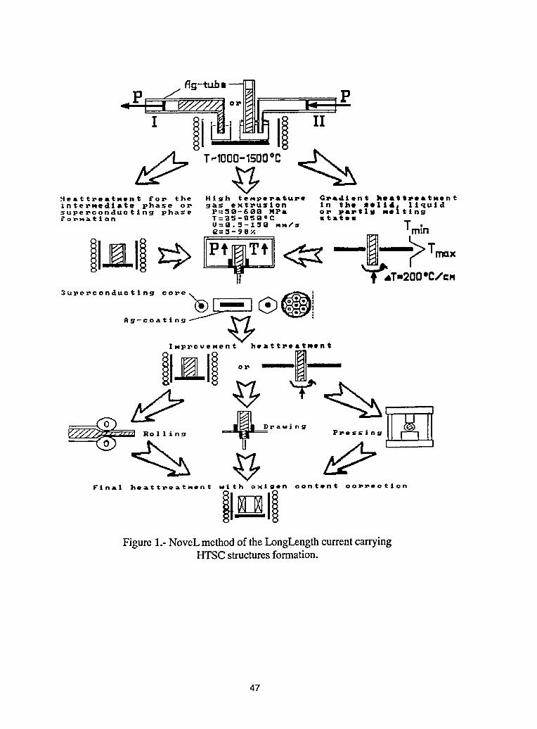
- 3 e a t t r e r t m r n t f o r t h e H i g h t e n p r r r t u r r C r r d i r n t L m a 8 8 r e r t m r n t i n t e r m e d i a t e p h a s e o r gas e x t r u s i o n in t h e s.114 l i q u i d s u p e r c o n d u o t i n g p h a s e P=S8-680 M P a o s p a r t l y n e f t i n g 2 o r n a t i o n T = a 5 - 8 5 B a C s t a t o r
u=e.5-158 mm/s Q=5-98%
S u p e r c o n d u c ti n g c o r e
A g - c o a t i n g
D r a w i n s P ~ e s s i n g
F i n a I h e a t t r e a t m e n t w i t h o x i s o n o o n t r n t o o ~ ~ r o t i o n
Bull Figure 1.- NoveL method of the LongLength current carrying
HTSC structures formation.
PREPARATION, STRUCTURE AND SUPERCONDUCTIVITY
OF HIGH-Tc COMPOUNDS
(Researchof high temperaturesuperconductorsin Hungary)
I. Kirschner
Departmentfor LowTemperaturePhysics,E0tv0sUniversity,Budapest,Hungary
Abstract
In this paper the main directions, methods and results of the investigationof high-Tcsuperconductorsin Hungaryarebrieflysummarized.Thefundamentalideaof this researchis to studythe effectof startingconditionson the microstructureof samplesand the influenceof the latter oneon their superconductingparameters. The investigationconcerningtechnical developmentis alsomentioned.
Introduction
At the beginning of this century the fundamental gravitation experiments of Lorfind
F_.6tv6sand his collaborators made the Hungarian physics to be well-known. Numerous
famous results are connected to his name, namely the E6tv6s-pendulum (which has an
importance in the research of raw materials too), Eftv6s-effect and E6tv6s-law, etc.
Before the 2nd World War the physical investigation was concentrated in the
universities and some big companies, dealing mainly with the applied research referring to
the actual needs of the industry. In this way important results have been achieved in the field
of research of metals (in particular of wolfram), noble alloys, and physical basis of the
production of incandescent lamps and high-power electrical equipments.
Many Hungarian originated physicists and chemists left their native country and
worked in the forefront of scientific research in different places of the world. Among them
Jen6 Wigner (nuclear physics), Ede Teller (nuclear physics), Mikl6s Kiirti (low temperature
physics), JAnos Kem6ny (discovery of basic language of computers), Liszl6 Tisza
48
(thermodynamics), Zolt,'inBay (radar technology), Frigyes B_/my (vestibular system), T6dor
K_m/m (mechanics, who was the founder of Jet Propulsion Laboratory), D6nes G_ibor
(holography), Le6 Szil_d (nuclear physics), Gy6rgy B6k6sy (research of hearing), J_os
Neumann (mathematics), J_inosPol_inyi (dynamics of chemical process), Korn61 IAnczos
(mathematical physics), Gy6rgy Hevesy (nuclear chemistry, isotope-traces), Albert
Szent-Gy6rgyi (biochemistry) and B_ilintTelegdi (nuclear physics) are the most known. The
excellent scientific results of Wigner, G_ibor,Szent-Gy6rgyi, Hevesy, B6k6sy, B_y and
Pol_inyiwere acknowledged by Nobel-prize.
During the years of fifties a new research and development system was established,
having four sections, namely university departments, institutes of the academy of sciences,
industrial research institutes and local research and development centers of different
companies.
The physical research broadened significantly and the directions covered almost all
of the main fields of physics, e.g. quantum-mechanics, solid state physics, thermodynamics,
nuclear physics, optics, astrophysics, elementary particles, statistical physics, laser physics,
relativity theory, etc.
Some groups were successful in different areas of physical research, namely in the
investigation of cosmic rays, molecular spectroscopy, crystal growth, elementary particles,
low energy nuclear physics, evolution of the world, magnetism, neutron physics, quantum
chemistry, etc. having internationally respected results.
Activity and co-operation in high-Tosuperconductivity
The solid state physics and materials science have a rather old tradition in Hungary,
and numerous Hungarian research institutions (universities, academic institutes and industrial
research centers) act in different fields of condensed matter physics. During this research,
remarkable results obtained concerning metals, alloys, semiconductors, surfaces and technical
application of the results of the fundamental study. This activity provided the basis of the
research of low temperature phenomena, first of all superconductivity.
The main themes of our superconductivity research were the investigation of the
magnetic properties of conventional superconductors, namely In-Bi, In-T1, In-Pb, Sn-Bi, and
Sn-Sb alloys, the study of compounds and alloys having an importance from the point of
view of application, building magnets and small-scale cable sections, the investigation of the49
pinning properties and the use of the irreversible thermodynamics to describe the features of
superconductors.
In the last years, after the discovery of the high-temperature superconductivity, we
turned mostly to the investigation of the phenomena of these new superconducting
compounds.
The investigation of the high-temperature superconductivity was started in Hungary
in January 1987, based on our former experiences obtained in the course of the research of
the conventional superconductors, which began in 1963.
(1). In a small country, like Hungary, the co-operation plays a very important role
in the research work, so we have organized a very wide cooperation inside and outside
Hungary concerning this field of science. This contains the following institutions:
1. Eight laboratories of the F_,6tviSsUniversity, Budapest, (Department for Low Temperature
Physics, Department of Atomic Physics, Department for General Chemistry, Department
for Mineralogy, Laboratory for Nuclear Chemistry, Department for Petrology and
Geochemistry, Laboratory for Surface Physics and Department for Analytical Chemistry),
2. Central Research Institute of Silicate Industry,
3. Five laboratories of the Budapest Technical University (Physical Institute, Reactor,
Department of Electrical Machines, Institute of Mechanical Technology and Department
of Electronics Technology),
4. Central Research Institute for Chemistry,
5. University of Debrecen (Institute for Experimental Physics),
6. Institute for Research of Metals,
7. Central Research Institute for Physics,
8. Research Institute of Electrical Industry,
9. EPOS-PVI Electrical Inc.,
10. University of Veszpr6m (Department of Silicate Chemistry),
11. Research Institute of Technical Physics,
12. National Bureau of Standards,
13. Nuclear Research Institute of the Hungarian Academy of Sciences,
14. Ministry of Industry (Ganz Electric, Budapest Iron and Steel Company, K6b_inya
Porcelain Works, Microelectronics Ltd, Metalltech Ltd),
15. Committee of Technical Development;50
16. Finland: Wihuri Physical Laboratory (University of Turku), Microelectronics Laboratory
(University of Oulu),
17. Great Britain: Center for HTSC (Imperial College of Science and Technology, London),
Department of Physics (Glasgow University),
18. Germany: Institut fiir Festkrrperforschung (KFA, Jiilich), Lehrstuhl fiir
Tieftemperaturphysik (Humboldt University, Berlin), Forschungszentrum (Geesthacht),
Hammelwerke Sensor GmbH (Scheweningen), Physikalisches Institut (University
Erlangen-Niirnberg, Erlangen),
19. The Netherlands: Physics Department, (University of Amsterdam), Physical Institute
(University of Nijmegen),
20. Russia: Institute for Physical Problems (Moscow), Institute of High Temperature
Research (Moscow),
21. Austria: Physikalisches Institut (University of Vienna),
22. Egypt: Department for Physics (Ain Shams University, Cairo),
23. USA: Institute of Chemistry, Drexel University, Philadelphia, etc.
(2). We have developed a complex basis for preparation of samples, which included
university laboratories, academic institutes, industrial research centers and local industrial
research-development sections. The preparation work covers different profiles, containing
different methods form the solid state reaction, through explosion procedure or screen
printing, until laser ablation.
(3). In the frame of the above mentioned co-operation we have sent superconducting
samples to Italy, Germany, England, The Netherlands, Russia, Austria for investigation and
provided more, than 100 Hungarian schools with them giving the possibility for the
demonstration of the impressive HTSC effects.
(4). A specific govemmental financial support helped us to increase the level of
investigation and made possible to carry out some experiments of that kind, which could not
be done earlier due to the lack of certain up-to-date experimental equipments.
Research and results in the field of HTSC
The research performed in Hungary in this field is basically experimental, it has,
however, some theoretical and application aspects, as well.
51
(1). The investigation can be treated as a complex one, because it concerns all of the
main directions in question, namely the sample preparation, physical properties and possible
technical applications.
(2). This study covers all of the known families of HTSC compounds. The properties
of La-Ba-Cu-O, Y-Ba-Cu-O, Bi(Pb)-Sr-Ca-Cu-O, T1-Ca-Ba-Cu-Oand in the latest time
Hg-Ba-Ca-Cu-O superconductors have been investigated. Different substitutions of ions and
doping processes were also performed, which is demonstrated as follows: Sr--.- Ba, Eu or
other RE--*-Y, Fe or Sn_Cu, F--*-02 and addition of Ag or LiF, in order to change the
physical or mechanical parameters of the basic superconducting compounds.
(3). The bulk samples, thick films and thin layers are equally in our interest from the
point of view of investigations.
(4). High-To superconductors, suitable to different specific purposes, (e.g. magnetic
screening) were elaborated, as elastic foils, rods and filaments, using organic and inorganic
filling materials.
(5). Certain improvements of the experimental technique were also performed
concerning the measurement of thermoelectromotive force, critical currents, a.c. resistivity
and susceptibility.
(6). During the different directions of investigation we used a rather wide spectrum
of the research methods, namely:
1. SEM, 2. X-ray, 3. TEM (HRTEM, SAED), 4. micro-probe, 5. EDS, 6. EPMA, 7. STM,
8. TG, 9. DTA, 10. resistivity measurements, 11. susceptibility, 12. SQuiD-technique,
13. ESR, 14. NMR, 15. thermodynamic cross-effect (TEMF, Hall),
16. magnetic (hysteresis), 17. dilatation, 18. SIMS, 19. detection of vortex movement,
20. ESCA, 21. M6ssbauer-spectroscopy, etc.
(7). The applied methods provide scientific information on the physical properties of
the samples, namely:
1. character of the superconducting transition (metallic, semiconducting, percolative),
2. sharpness of it, 3. effect of preparation (starting materials, their mixture, heat treatment),
4. temporal stability or instability (possible change in structural, electrical and magnetic
properties), 5. effect of external circumstances, 6. quantity of superconducting material in
specimens, 7. number, quality and share-rate of s.c. phases, 8. place and change of ions,
9. type of charge carriers, 10. degree of oxidation, 11. chemical co-ordination, 12. properties
of surfaces and grains, 13. critical parameters (To, T_ To, Hc_,Jci, _, h, K), 14. phonon-
52
electron coupling, 15. gap, 16. conclusion on the fundamental superconducting mechanisms,
17. data for unit cells and their deformation, 18. anisotropy, 19. mechanical properties,
dilatation, elasticity, 20. influence of thermal cycling, 21. corrosion, degradation, etc.
(8). Due to the limited length of this paper only a few concrete results of the
Hungarian HTS-research can be enumerated to demonstrate the scope of it:
1. Just from the beginning we made the electrical and magnetic measurements together
to obtain a good chance to evaluate the Meissner's state volume of samples.
2. We have investigated in detail some important questions of high-Tocompounds, namely
the preparative chemistry consequences on Y-Ba-Cu-O superconductors, the possible role
of percolation effects in establishment of superconductivity, characteristic parameters of
T1-Ca-Ba-Cu-Ocompounds based on a very wide spectrum of preparation methods, surface
structure of different samples by STM method, effect of thermo-mechanical and water
corrosion, proximity effect, complex study of Bi-based samples, effect of neutron
irradiation, diamagnetism above To, effect of particle size on the mechanism of the
development of HTSC, improvement of the plastic properties of samples, etc.
3. Similarly to other laboratories, we also observed superconductivity at higher, than usual
To in an Y-based, temporally unstable specimen in April, 1987, but in contrast with other
results, the value of its Tc was only 105 K.
4. The elaboration of superconducting ceramic magnets with a new energy feeding, small-
scale electrical rotating machines, cryogenic liquid level sensors, magnetic field detectors
and magnetically screening elastic foils, rods and thin filaments can be mentioned among
our works for the purpose of technical development.
5. Some Hungarian researchers were dealing with the study and application of Josephson's
tunnelling and with the high-To SQUID experiment having some new and valuable
information on these questions and on their application in measuring technique.
6. The employment of the M6ssbauer-spectroscopy to find out the details of structure and
some fine effects represents an important contribution to the HTSC-research in Hungary.
It was very wide, and based on replacing sites by 151Eu,_19Sn,57Feand 57Conuclides in
order to get information about site preference, structural changes, temporal instability and
change of the phonon properties.
7. Hungarian researchers have attained remarkable results in the investigation of fullerenes,
certain part of those can be superconducting. If the chains of C60 molecules contain some
alkaline metals (e.g. K, or Rb), they can develop in the form of filaments and produce
53
electrically conducting polymer-crystals, which show a metallic behaviour.
This research is also accomplished in an international (American and Swiss) co-operation.
The structure of fullerenes of different kinds of conductivity are under
investigation in Hungary, using unlike methods, e.g. ESR-, IR-, and
M6ssbauer-spectroscopy. These investigations include alkaline fullerenes, fullerene
polymers and ligandum-containing fullerenes as well.
8. Optically induced changes of the magnetic properties, created by laser beam in
La-Ba-Cu-O superconductors have been observed. According to our investigation, the
light-induced change of the magnetic moment strongly depends on the temperature at low
temperatures. The results obtained in the magnetic field of 1-26 Oe suggest, that the
observed effects have contributions from the weakening Josephson's junctions under
illumination and from the additional part of the optically induced flux creep, which
depends on the applied magnetic field.
9. In order to examine the fine details of superconducting-normal or normal-superconducting
transition, a new, so-called thermometric mapping method was elaborated. By the essence
of this method, the samples are submitted to a large and variable temperature gradient,
which broadens significantly the transition to reveal its gradual nature. This procedure is
in a strong contrast with the conventional electrical and magnetic measuring practice of
superconductivity, where a homogeneous temperature distribution is used generally to
avoid the uncertainty of results. The method is sensitive enough to detect not only the fine
structure of the transition, or to select the unlike properties of different specimens, but to
trace the change of the features of a given sample too.
(9). Comparing to the international research of HTSCs, we investigated firstly some
important questions of this field, which were as follows:
1. building high-Tosuperconducting ceramic magnets, 2. synthesis and application of a new
precursor Ba2Cu3Os, 3. investigation of the corrosion effects, 4. elaboration of the
thermometric mapping method, 5. Mrssbauer-study of Tl-based superconductors,
6. cryogenic liquid level sensor based on TEMF, 7. a new method for preparing Y-based
superconductors, 8. observation of the fine structure of S-N or N-S transition, and
9. elaboration of a microwave magnetic field detector. At the same time Hungarians were
among the first groups to measure TEMF, to develop ceramic HTSCs workable by machine-
tool, to elaborate elastic foils, rods and filaments and to build small electrical rotating HTSC
machines.
54
Publications
In the course of investigation of high-To superconductors we have reached
internationally respected results, published over 150 scientific papers, elaborated some
patents and introduced the fundamental phenomena of high-temperature superconductivity
into the education of universities and secondary schools. Among them, we have the exact
number of the publications of one of the Hungarian high-To laboratories. This is the
Department for Low Temperature Physics, Ertvrs University, which published 75 scientific
papers, 3 patents and 15 studies and dissertations on the methods, results and applications
between 1987 and 1993.
Conclusions
On the basis of the facts analyzed in this paper, certain conclusions can be drawn, as
follows:
1. A small country can also be effective in the field of a given branch of scientific
research, if the aim is chosen right, the powers are concentrated rationally and the co-
operations are organized operatively [1].
2. Hungarian scientists attained significant results in different areas of high-To
superconductivity and contributed successfully to the world-wide research, because they
utilized effectually the internal and the possibilities of international co-operations [2].
References
1. I. Kirschner, J. B_kuti, M. Gilland K. Torkos, Phys. Rev. B36. 2313. 1987.
2. I. Kirschner,S. Lepp_ivuori,R. Laiho, A.D. Caplin,T. K_mAn, E. Lfthderanta,
G. Zsolt, A. Uusim_ki,J. Laverty,T. Porjesz, I. Hal_iszand Gy. Kov_ics,
Zeitschr. Phys. B78. 381. 1990.
55
mGH-T SUPERCONDUCTORS: TECHNICAL AND COMMERCIAL
CHALLENGE
I. Kirschner _), E. Horv_ith_2),I. Vajda_), L. Bencze_4)and N. Giibl_4)
(1) Department for Low Temperature Physics, EOtvOsUniversity, Budapest, Hungary(2) EPOS-PVI, Inc., Budapest, Hungary
(3) Department of Electrical Machines, Technical University, Budapest, Hungary(4) Research Institute for Electrical Industry, Budapest, Hungary
Abstract
Somebasicquestionsof the way, whichleadsfrom the discoveryof high-Tosuperconductorsto their applications is surveyed. The influenceof high-T_superconductingtechnology on theindustrialand socialdevelopmentis also brieflyanalysed.
General
The main problems are how the results of the scientific research can be transferred
"into technology and in what extent this process can be useful for the society.
Postulation: Superconductivity, as a phenomenon of extremely or ideally lossless state
should revolutionize not only the electrical or electronical industry, but through them it
should change various segments or sections of technology and the life style of the society
too.
The fact: There are certain obstacles (requirement of cooling, critical parameters
themselves, a.c. losses, etc.) those make difficult to introduce the physical findings, results
and developments into technology.
Disappointments: Some potential users, evenprofessionals (engineers, managers, etc.)
are often deeply disappointed when they are aware of the difficulties.
Financing : Both of basic and technical researches require sponsors who are able and
eager to invest money into a scientific program without the requirement of making profit
within a short term. Govemments and companies of developed countries wish to sponsor
these themes, but in an other part of countries there is a lack of money to support the
superconductivity research.56
Usefulness: The new technology induced by the research of superconductivity results
in new and efficient modes of production. This leads to bring forth new values for the
society.
Superconducting products
Fifty years were necessary after the discovery of conventional superconductivity [1]
until the first attempt [2] to elaborate some magnetic application of this phenomenon. The
main difficulty is represented by complicated and expensive liquid helium technique which
strongly limits the spread of low-temperature superconductors.
A qualitatively new situation appeared by the discovery of high-temperature
superconductivity [3], for which the simple and cheap cooling provided by liquid nitrogen
is sufficient. Until this date five groups of oxide ceramics can be taken into consideration
from the point of view of technical employment, namely La-Ba-Cu-O, Y-Ba-Cu-O,
Bi(Pb)-Sr-Ca-Cu-O, T1-Ca-Ba-Cu-Oand Hg-Ba-Ca-Cu-O families having intervals of critical
temperature Tc of 32-40 K, 80-92 K, 85-110 K, 60-125 K and 90-150 K, respectively.
As far as the other two main parameters are concerned, the upper critical magnetic field He2
falls into interval of 50-200 T, while the transport critical current density Jc extremely
depends on the morphological character of the samples [4], having values of 100-300 A/cm2
for bulk materials, 103-105A/cm2 for melt-textured thick films and 105-106A/cm2 for high
quality thin layers.
The reliable and controlled best values of Jofor 100-200 m long wires and tapes are
50000-100000 A/cm2 for Y-based, 50000-150000 A/cm2 for Bi-based materials, while
10000-20000 A/cm_ can be reached for very pure Tl-based short samples. Since some of
these superconductors can work in a very high (5-25 T) magnetic field, the possibility of
their use for different electrotechnicalpurposes can be taken to be acceptable.
The problem of rigid andbrittle properties of these ceramics and the question of long
time stability seems to be soluble.
The most probable applicationsof these materials concern not only the electrical
industry, but the electronics, signalprocessing, computer techniqueand informatics too, as
is listed in the followings [5]:
1. building magnetsand magneticshieldings,
2. generators, electrical transport lines, magneticenergy storage,
57
3. fault current limiters,
4. heavy-duty bearings,
5. magnetically levitated machines,
6. sensors for temperature, pressure, magnetic field, frequency, voltage, current, liquid level,
radiation, etc.,
7. signal detectors and processors,
8. electronical chips,
9. high frequency receivers, mixers and antennas,
10. fast computers,
11. bolometers and nuclear particle detectors, etc.
New developments: Proposals and experiments regarding technical applications of
high-To superconductors should compete with existing and reliable products. The new
products should have some advantages to substitute the present ones.
Most successful applications have been developed in those fields of technology, where
there are no real competitive counterparts.
Commercial challenge
The commercial challenge arises when superconducting products are at the society's
disposal in an appropriate quality and quantity and they should be distributed among the
demanding institutions and persons by selling and buying. Nowadays we are far from this
point, but the society must be prepared to this one, because the new materials, products,
instruments and equipments will change the style and quality of the life.
Superconductivity and society
How to influence the society in order to accept easier the novel and unique results of
the science and technology?
We think there is a lack of a thorough analysis of economic and social effects of the
technology of superconductivity. This analysis must be accomplished by ourselves and its
results should be submitted to the decision-making persons.
It is obvious that we are responsible to introduce the teaching of basic and applied
58
aspectsof superconductivityinto the educationof the universitiesand secondaryschools or
to improve theireducation.Numerousprojectsaimedat the applicationof superconductivity
are planned to be partly or fully completedby the end of this century. By this time the
studentswho will study the superconductivityin the next years will come to work into the
industry, economy, etc., and perhaps theywouldbe moresusceptibleto new technologies,
like superconductivity.
References
1. K. H. Onnes, Comm. Phys. Lab. Univ. Leiden N° 119. 122. 1911.2. J. E. Kunzler, E. Buehler, F. S. L. Hsu and J. H. Wernich, Phys. Rev. Lett. 6. 89.
1961.3. J. G. Bednorz and K. A. MOiler, Zeit. Phys. B64. 189. 1986.4. I. Kirschner, Appl. Supercond. 1. 1785. 1993.5. I. Kirschner, S. Lepp_ivuori, T. Porjesz, A. Uusim_ikiand T. Kokkom_ki, Sensors and
Actuators A41. 58. 1994.
59
Technical and Commercial Challengesin High Tc SQUIDs and Their Industrial Applications
RoundtableDiscussionSessionTheFourthWorldCongresson Superconductivity
D.F. LuMidwestSuperconductivityInc.
Lawrence,KS66049
A SQUID is the most sensitivedevice for measuringchanges in magneticflux. Since itsdiscoveryin the sixties,scientistshavemadeconsistenteffortsto applySQUIDsto variousapplications.Instrumentsthat are the most sensitivein their respectivecategorieshavebeenbuilt, suchas SQUIDDCsusceptometerthat is nowmanufacturedbyQuantumDesign,pico-voltmeterwhichcould measure10-14volts, and gravitational wave detectors. One of the most successfulapplicationsof SQUIDs is inmagnetoencephalography,a non-invasivetechnique for investigatingneuronal activity in the livinghuman brain. This technique employs a multi-channelSQUID magnetometerthat maps the weakmagneticfield generatedby smallcurrentwheninformationis processedin brain, and its performanceismarvelous.
All the wondersof SQUIDshavebeen realizedusing low temperaturesuperconducting(LTS)SQUIDs that must be cooled using liquid helium. Since the discovery of high temperaturesuperconductorsin 1986, people have long expectedto replace LTS SQUIDswith their high Tccounterpartsin some applications,or to find new applicationsfor high temperature superconducting(HTS)SQUIDs.A HTS SQUIDis capableof workingat liquidnitrogentemperature,whichis far moreadvantageousto liquid helium in terms of cost and in terms of possibilityfor field applications.Manyeffortshave been made to take advantage of HTS SQUIDs.Varioustypes of HTS thin film or bulkSQUIDmagnetometersand gradiometershavebeen studied.The bestHTS SQUIDis very competitivewith its LTS counterpart in properties and performance.However, there has not been any realcommercialapplicationof HTS SQUIDsyet. Despitethe promisingfeaturesof HTS SQUIDs,there arestill many challengesahead beforeHTS SQUIDscan be widelyused in commercialproducts. In thisshort paper, we would like to brieflydiscusssome of the issuesthat people need to be concernedwithwhentryingto usea HTSSQUIDin a particularapplication.
First of all, peoplehave to ask themselvesin what typeof applicationsthat a HTS SQUIDhasadvantagesover other techniques.Althougha SQUIDdevice is more sensitive,the cost involved isgenerally higher and the requirementof knowledgeto operate a SQUID device is more stringent.Therefore,people needto determinefor themselveshow competitivea SQUIDdeviceis comparedwithother techniques.How much better is it to use a HTS SQUIDin a particular applicationthan thosecurrentlyused systems?Howmuch improvementcan we expectover other techniquesif we use a HTSSQUIDin that application?Is the improvementsubstantialthat it can be easilyacceptedand adoptedbyend users? As Weinstockalways points out, one should not use a SQUID-basedinstrumentwhen asimplertechnologywill suffice[1].
Supposethat a SQUID is a necessityfor an application,should a HTS SQUIDbe used? Forinstance, can a HTS SQUID replace a LTS SQUID in susceptometers,gravitational wave detectorswithout or with only little compromise?Comparedwith LTS SQUIDs,HTS SQUIDshaveonly one bigadvantage.That is, it has a higher transitiontemperatureand it can work at liquidnitrogen temperatureinsteadof liquidheliumtemperature.This is muchpreferredeconomically,and it doesopen doorsto a lotof possible uses of HTS SQUIDs.However,as pointed out by John Clark, a SQUIDworking at thistemperaturewillnever achieveas gooda resolutionas can theircounterpartsworkingin liquidhelium [2].
60
At the same time, sincehigh temperaturesuperconductorsare ceramics,they are muchmore difficulttoprocessthan low temperaturesuperconductors.A superconductingtransformermade of high Tc wiressimilar to low Tc transformers,whichhelpsto placeSQUIDsin a magneticallyshieldedenvironment,hasnot been realized. A HTS SQUID gradiometer cannot be made as symmetric as a LTS SQUIDgradiometer,which achievesone part per million in symmetry.Thus, it wfUbe very hard for HTSSQUIDsto replaceLTS SQUIDsforsensitivemeasurements.
Nevertheless,we need to realize that there are still many other applications in which thesensitivitiesof HTS SQUIDswill suffice.For these applications,we must take full advantagesof hightransition temperaturesof HTSSQUIDs.If they are combinedwith smallsize cryocoolers,portableHTSSQUIDdevicesmay becomepossiblefor field and industrial applications.This cannotbe accomplishedwith LTS SQUIDs.
Of course,to applyHTSSQUIDsforfieldor industrialapplications,manypracticalmattersneedto be taken care of. The immediate concern for field applications is that a SQUID is subject toenvironmentalnoises,suchas interferencefrompowerline,machinery,electronicequipment,and etc. It isnot like thosebiomagneticinstrumentsandthose scientificinstntmentswherealmosteverything,such asSQUIDsensors,superconductingtransformers,and eventhe sample,is enclosedin a magneticshieldedroom. Thereforethe field sensedby the SQUIDsensorsis very small, and is all the informationpeoplewant. Everythingdetectedis useful.For fieldor industrialapplications,there is no shielded roomto use.Otherwiseit cannot be portableor the cost involvedis too much.Withoutany shielding,the SQUIDisexposedto a large environmentalfield or interference.The interferencein general is alternating fieldswhich rendera SQUIDmagnetometersimplynot usablesincemost of SQUIDelectronicshas a range ofonly _t.500_0,while the fluxproducedby the interferencemay be hundreds times larger. The SQUIDelectronicsjust has to reset itself too frequentlyto be usable.HTS SQUIDgradiometersmay be used.However,they are also influencedby the interferencedue to limitedsymmetry.This difficultyhas to beovercomefor HTS SQUIDsto havea big market. Techniquesmay involveredesignor modificationofelectronics.
The largeenvironmentalnoisealsoaffectsthe propertiesof a SQUIDitself.In almostall the LTSSQUIDapplications,the SQUIDis placed in a shieldedchamberand the surroundingfield is tiny. Themeasuredsignalis transformedbya superconductingtransformerwith the pick-upcoil placedoutsidetheshieldedchamber.But forhigh temperaturesuperconductors,sucha flexiblesuperconductingtransformercannot be fabricatedyet. A HTS SQUID has to be exposed to external field, even with thin filmtransformers.Whenit is exposed,manyof its propertiesmaychangedependingon the magnitudeof thefield.For instance,the criticalcurrentin thejunctionmayvarywith the appliedfield,whichwill certainlyaffectthe SQUIDproperties.At the same time, for high temperaturesuperconductors,flux trappingmaybe quite importantin largefield,thus causinglargenoises.
It is usually expectedthat a devicewith a HTS SQUIDperformsbetter than those withoutSQUIDsin many applications.It shouldbe able to do what the current systemscannot do. It shouldbeable to detectevensmallersignals.While talking aboutpossiblebenefitsthey mayobtainwith a SQUID,peopleoftentend to omit the fact that the signalto noiseratiois reducedfor small signals.Althoughthenoise may be smaller than currentlydetectablesignal, will it overwhelmthe expectedsmaller signaldetectableonly by SQUIDs?If it does,the sensitivityof SQUIDscannotbe fullyutilized.Peopleneedtofind a way to reduce the noise further to improvethe signal to noise ratio. I will take nondestructivetestingof metalas an example.Theconventionaleddycurrentmethodis not ableto detectsmallcracksata depth greaterthan 0.5 inches.We are workingon using a I-ITSSQUIDas a sensorto replace the coilsensorin conventionaleddy currentmethodfordetectionof smallcracksat large depth. Since our targetcrack(hereafterthe target)is fartherfromthe coilthanthe crack(hereafterthe crack)that canbe detectedusing conventionaleddy currentmethod,the currentdensityinducedat the targetis smallerthan that atthe crack. Similarly, since the target is also farther from the sensorthan the crack, the field change
61
generatedbythe targetdecaysfasterthan bythe crack.Becauseofthese factors,the signalfrom the targetis much smaller.However,the noiselevel remainsthe same.The effectof changein lift-off,the distancebetweentilecoil or sensorand the sample,is still largewith the eddycurrentmethod.If such a change inlift-offcannotbe controlled,it will generatea noisethat maybe muchgreaterthan the signalgeneratedbythe target.Usefulsignalwillbe buriedin the noise.Thismaybe more importantpracticallythan the noiseof a SQUIDsystem.
There are of course many other things people need to consider and discuss for specificapplications.There is a bright futurefor SQUIDapplicationsin industry,there are alsoa lot of things tobe donebeforeit becomesa reality.Overall,researchershave to studythe particularapplicationstheyareinterestedin, andmakeall necessaryadjustmentsto buildusabledevices.
I sincerely thank the organizing committee for inviting me to speak at the "RoundtableDiscussionSession."I am also gratefulto Prof. K. W. Wongfor valuablesuggestions.Finally, I wouldlike to thank MidwestSuperconductivityInc. for the support.
References:
1. H. Weinstock, Physica C 209, 269 (1993)H. Weinstock, 1EEE Trans.Mag. 27 3221 (1991)
2. J. Clarke, Scientific American, August Issue, p. 46 (1994)
62

Accelerator Technology
Chair: Dr. Siegfried Wolff

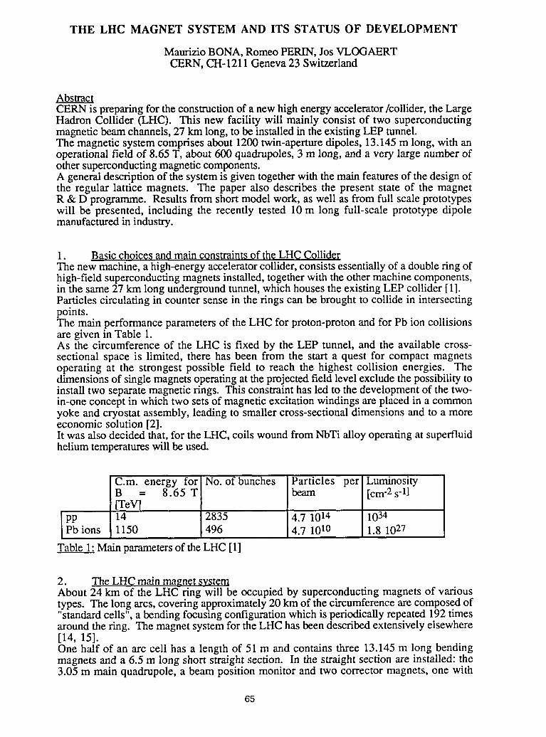
THE LHC MAGNET SYSTEM AND ITS STATUS OF DEVELOPMENT
MaurizioBONA, Romeo PERIN,JosVLOGAERTCERN, CH-1211 Geneva 23 Switzerland
Abstrac[CERN is preparing for the construction of a new high energy accelerator/collider, the LargeHadron Collider (LHC). This new facility will mainly consist of two superconductingmagnetic beam channels, 27 km long, to be installed in the existing LEP tunnel.The magnetic system comprises about 1200 twin-aperture dipoles, 13.145 m long, with anoperational field of 8.65 T, about 600 quadrupoles, 3 m long, and a very large number ofother superconducting magnetic components.A general description of the system is given together with the main features of the design ofthe regular lattice magnets. The paper also describes the present state of the magnetR & D programme. Results from short model work, as well as from full scale prototypeswill be presented, including the recently tested 10 m long full-scale prototype dipolemanufactured in industry.
1. Basic ch0ices and main constraintsof the LHCColliderThe new machine, a high-energy accelerator collider,consists essentially of a double ring ofhigh-field superconducting magnets installed, together with the other machine components,in the same 27 km long underground tunnel, which houses the existing LEP collider [1].Particles circulating in counter sense in the rings can be brought to collide in intersectingpoints.The main performance parameters of the LHC for proton-proton and for Pb ion collisionsare given in Table 1.As the circumference of the LHC is fixed by the LEP tunnel, and the available cross-sectional space is limited, there has been from the start a quest for compact magnetsoperating at the strongest possible field to reach the highest collision energies. Thedimensions of single magnets operating at the projected field level exclude the possibility toinstall two separate magnetic rings. This constraint has led to the development of the two-in-one concept in which two sets of magnetic excitation windings are placed in a commonyoke and cryostat assembly, leading to smaller cross-sectional dimensions and to a moreeconomic solution [2].It was also decided that, for the LHC, coils wound from NbTi alloy operating at superfluidhelium temperatures will be used.
C.m. energy for No. of bunches Particles per LuminosityB = 8.65 T beam [cm-2s-ll[WeV]
pp 14 2835 4.7 1014 1034Pb ions 1150 496 4.7 1010 1.8 1027
Table 1: Main parameters of the LHC [1]
2. TheLHCmainmagnetsystemAbout 24 km of the LHC ring will be occupied by superconducting magnets of varioustypes. The long arcs, covering approximately 20 km of the circumference are composed of"standard cells", a bending focusing configuration which is periodically repeated 192 timesaround the ring. The magnet system for the LHC has been described extensively elsewhere[14, 15].One half of an arc celi has a length of 51 m and contains three 13.145 m long bendingmagnets and a 6.5 m long short straight section. In the straight section are installed: the3.05 m main quadrupole, a beam position monitor and two corrector magnets, one with
65
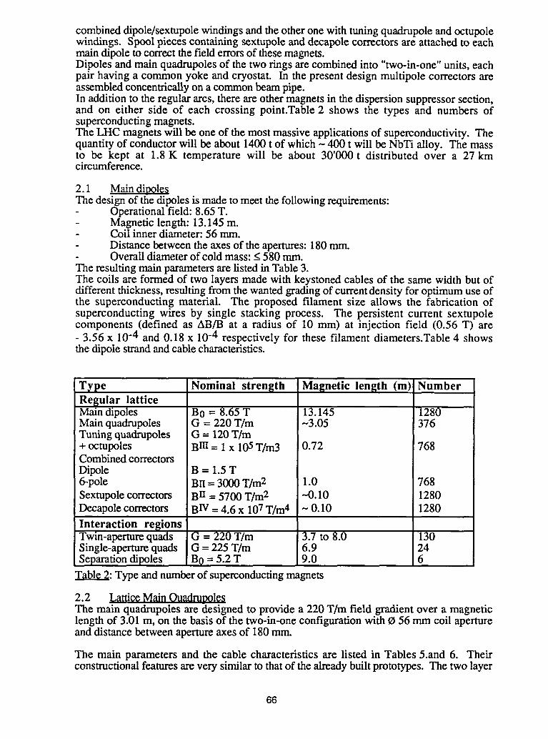
combined dipole/sextupole windings and the other one with tuning quadrupole and octupolewindings. Spool pieces containing sextupole and decapole correctors are attached to eachmain dipole to correct the field errors of these magnets.Dipoles and main quadrupoles of the two rings are combined into "two-in-one" units, eachpair having a common yoke and cryostat. In the present design multipole correctors areassembled concentrically on a common beam pipe.In addition to the regular arcs, there are other magnets in the dispersion suppressor section,and on either side of each crossing point.Table 2 shows the types and numbers ofsuperconducting magnets.The LHC magnets will be one of the most massive applications of superconductivity. Thequantity of conductor will be about 1400 t of which ~ 400 t will be NbTi alloy. The massto be kept at 1.8 K temperature will be about 30'000 t distributed over a 27 kmcircumference.
2.1 Main ¢lip91_The design of the dipoles is made to meet the following requirements:- Operational field: 8.65 T.- Magnetic length: 13.145 m.- Coil inner diameter: 56 ram.- Distance between the axes of the apertures: 180 mm.- Overall diameter of cold mass: < 580 mm.The resulting main parameters are listed in Table 3.The coils are formed of two layers made with keystoned cables of the same width but ofdifferent thickness, resulting from the wanted grading of current density for optimum use ofthe superconducting material. The proposed filament size allows the fabrication ofsuperconducting wires by single stacking process. The persistent current sextupolecomponents (defined as AB/B at a radius of 10 mm) at injection field (0.56 T) are- 3.56 x 10⁻⁴ and 0.18 x 10⁻⁴ respectively for these filament diameters.Table 4 showsthe dipole strand and cable characteristics.
Type Nominal strength Magnetic length (m) NumberRegular latticeMain dipoles B0 "- 8.65 T 13.145 1280Main quadrupoles G = 220 T/m -3.05 376Tuning quadrupoles G = 120 Tim+ octupoles BIll= 1 x 10⁵T/m3 0.72 768Combined correctorsDipole B = 1.5 T6-pole BII -- 3000 T/m2 1.0 768Sextupolecorrectors BII -- 5700 T/m2 -..0.10 1280Decapole correctors B1V= 4.6 x 10⁷T/m4 - 0.10 1280
Interaction regionsTwin-aperture quads G = 220 T/m 3.7 to 8.0 130Single-aperture quads G = 225 T/m 6.9 24Separation dipoles B0 ---5.2 T 9.0 6
Table 2: Type and number of superconductingmagnets
2.2 Lattice Main OuadrupolesThe main quadrupoles are designed to provide a 220 T/m field gradient over a magneticlength of 3.01 m, on the basis of the two-in-one configuration with _ 56 mm coil apertureand distance between aperture axes of 180 mrn.
The main parameters and the cable characteristics are listed in Tables 5.and 6. Theirconstructional features are very similar to that of the already built prototypes. The two layer
66
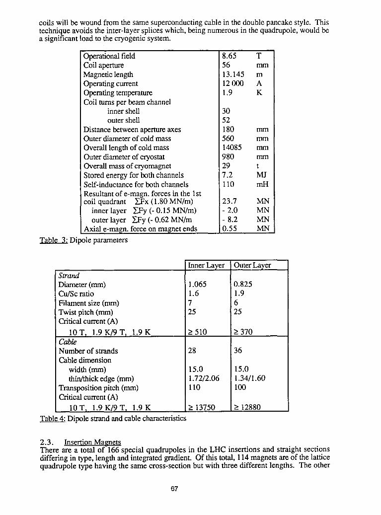
coils will be wound from the same superconducting cable in the double pancake style. Thistechnique avoids the inter-layer splices which, being numerous in the quadrupole, would bea significant load to the cryogenic system.
Operational field 8.65 TCoil aperture 56 mmMagnetic length 13.145 mOperating current 12 000 AOperating temperature 1.9 KCoil turns per beam channel
inner shell 30outer shell 52
Distance betweenaperture axes 180 mmOuter diameter of cold mass 560 mmOverall length of cold mass 14085 mmOuter diameter of cryostat 980 mmOverall mass of cryomagnet 29 tStored energy for both channels 7.2 MJSerf-inductancefor both channels 110 mH
Resultant of e-magn, forces in the 1stcoil quadrant _...Fx(1.80 MN/m) 23.7 MN
inner layer _,Fy (- 0.15 MN/m) - 2.0 MNouter layer ,_,Fy(- 0.62 MN/m - 8.2 MN
Axial e-ma_n, force on magnet ends 0.55 MNTable 3: Dipole parameters
Inner La_,er Outer LayerStrandDiameter (mm) 1.065 0.825Cu/Sc ratio 1.6 1.9Filament size (mm) 7 6Twist pitch (mm) 25 25Criticalcurrent (A)
10T_ 1.9K/9T r 1.9K >510 >370Cab/eNumber of strands 28 36Cable dimension
width (mm) 15.0 15.0thin/thickedge (ram) 1.72/2.06 1.34/1.60
Transposition pitch (mm) 110 100Criticalcurrent (A)
10 T, 1.9 K/9 T, 1.9 K > 13750 >_12880
Table 4: Dipole strand and cable characteristics
2.3. Insertion MagnetsThere are a total of 166 special quadrupoles in the LHC insertions and straight sectionsdiffering in type, length and integrated gradient. Of this total, 114 magnets are of the latticequadrupole type having the same cross-section but with three different lengths. The other
67
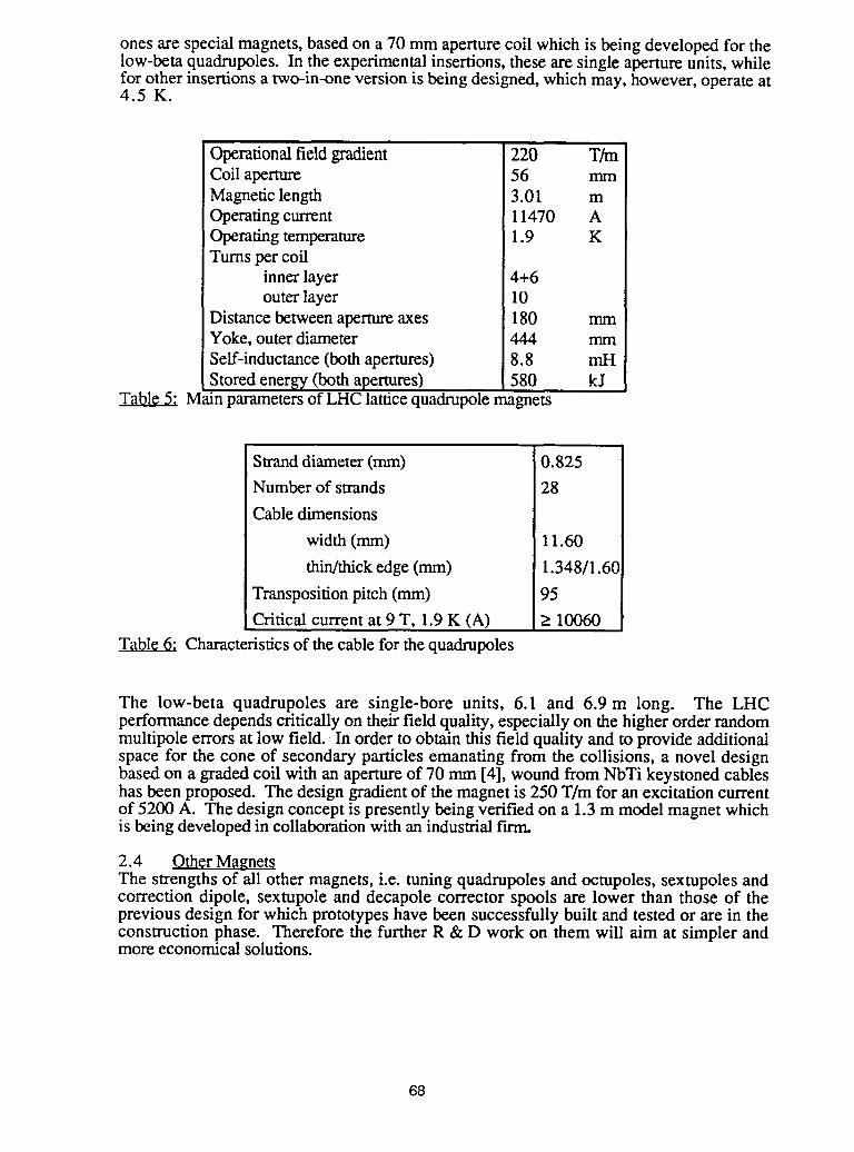
ones are special magnets, based on a 70 mm aperture coil which is being developed for thelow-beta quadrupoles. In the experimental insertions, these are single aperture units, whilefor other insertions a two-in-one version is being designed, which may, however, operate at4.5 K.
Operational field gradient 220 T/mCoil aperture 56 mmMagneticlength 3.01 mOperatingcurrent 11470 AOperatingtemperature 1.9 KTurns per coil
inner layer 4+6outer layer 10
Distance between aperture axes 180 mmYoke, outer diameter 444 mmSelf-inductance (both apertures) 8.8 mHStored energy (both ape_res) 580 kJ
Tal_le5: Main parameters of LHC lattice quadrupole magnets
Strand diameter (mm) 0.825Number of strands 28
Cable dimensions
width (mm) 11.60
thin/thickedge (mm) 1.348/1.60
Transposition pitch (mm) 95Critical current at 9 T, 1.9 K (A) > 10060
T_l_le6: Characteristics of the cable for thequadrupoles
The low-beta quadrupoles are single-bore units, 6.1 and 6.9 m long. The LHCperformance depends critically on their field quality, especially on the higher order randommultipole errors at low field. _In order to obtain this field quality and to provide additionalspace for the cone of secondary particles emanating from the collisions, a novel designbased on a graded coil with an aperture of 70 mm [4], wound from NbTi keystoned cableshas been proposed. The design gradient of the magnet is 250 T/m for an excitation currentof 5200 A. The design concept is presently being verified on a 1.3 m model magnet whichis being developed in collaboration with an industrial firrn.
2.4 Other MagnetsThe strengths of all other magnets, i.e. tuning quadrupoles and octupoles, sextupoles andcorrection dipole, sextupole and decapole corrector spools are lower than those of theprevious design for which prototypes have been successfully built and tested or are in theconstruction phase. Therefore the further R & D work on them will aim at simpler andmore economical solutions.
68
3. Status of the LHC magnet developmentThe programme was mainly focused on the standard cell components and in particular onthe dipoles, but included study and construction of several other magnets and items.
3.1 Quadrupole_Two full size quadrupole magnets of final aperture (56 mm) and length (3.05 m) have beendesigned and built by CEA-Saclay, using s.c. cables and structural parts made in industry.Their design and construction are described in [10].These magnets have undergone tests at 1.9 K and magnetic measurements at CEA-Saclay bythe end of 1993. Both prototypes have reached the design current, the In'st magnet after onequench, the second one after three quenches.After testing, the first prototype has been delivered to CERN where it is presently beinginstalled into a "short straight section", which is an assembly of quadrupoles, sextupolesand all other types of correction magnets. This will be the f'trstelement to form the test string(one half standard cell) of the LHC which is expected to be ready for testing by end 1994.The collaboration between CERN and CEA-Saclay has permitted to develop a set of toolingin view of the mass production to be performed in industry.
3.2 o_02m!The R & D effort covers:- Superconducting cables.- Short single-aperture and twin-aperture models (- 1.3 m long).- Long twin-aperture prototypes (- 10 m long).
3.2.1 Superconducting cablesTwenty-four kilometres of cable for the inner coil shell made of 26, 0 1.29 mm strands,and 42 kilometres of cable for the outer coil shell, made of 40, 0 0.84 mm strands, havebeen developed and produced by the five European manufacturers and at present satisfy allmain technical requirements. The current densities in the non-copper part of the strandcross-section, taken from the finished cables at the 3 G limit in the distribution curve ofproduction, are 980 A/mm2 at 8 T, 4.2 K, for the inner layer and 2000 A/ram2 at 6 T,4.2 K, for the outer layer. The results of the models show that the short sample quenchingfield of the dipole (Bss) is close (within ~ 2%) to the cable short sample limit determinedfrom strands extracted from the cables.The total quantity produced, 14 t, is a significant amount and gives confidence that therequired quality can be maintained in mass production.
3.2.2 Model magnetsA number of models of the main dipoles have been made and successfully tested [5, 6, 7].Two magnets were built in Japan by KEK in collaboration with industrial companies. Allother magnets were entirely built by European companies except one which was assembledat CERN using industry made coils and other components.At 4.3 K, the conductor short sample limit of this magnet was attained at the second quenchand no retraining occurred after thermalcycles.At 2 K the magnet had the first quench above 9 T central field, reached 9.5 T in fivequenches and finally attained the record field of 10.5 T. After thermal cycles to roomtemperature all quenches were above 9.75 T.
3.2.3 Ten m¢Ix_long ma_etsA magnet, named TAP, with a CERN twin structure but coils identical to those of theHERA dipole (75 mm aperture) was built in industry and successfully tested at CEA-Saclayat the nominal temperature of 1.9 K at which the conductor short sample limit of 8.3 T wasreached [8].
69
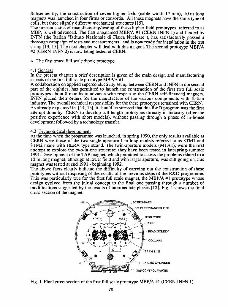
Subsequently, the construction of seven higher field (cable width 17 mm), 10 m longmagnets was launched in four firms or consortia. All these magnets have the same type ofcoils, but three slightly different mechanical structures [15].The present status of manufacturing/testing of these higher field prototypes, referred to asMBP, is well advanced. The first one,named MBP/A #1 (CERN-INFN 1) and funded byINFN (the Italian "Istituto Nazionale di Fisica Nucleare"), has satisfactorily passed athorough campaign of tests and measurements, and is now ready for installation in the teststring [13, 15]. The next chapter will deal with this magnet. The second prototype MBP/A#2 (CERN-INFN 2) is now being tested at CERN.
4. The first tested full scale dipole prototyp_
4.1 GeneralIn the present chapter a brief description is given of the main design and manufacturingaspects of the first full scale prototype MBP/A #1.A collaboration on applied superconductivityset up between CERN and INFN in the secondpart of the eighties, has permitted to launch the construction of the first two full scaleprototypes about 8 months in advance with respect to the CERN self-financed magnets.INFN placed their orders for the manufacture of the various components with Italianindustry. The overall technical responsibility for the these prototypes remained with CERN.As already explained in [14, 15], it should be stressed that this R&D program was the firstattempt done by CERN to develop full length prototypes directly in Industry (after thepositive experience with short models), without passing through a phase of in-housedevelopment followed by a technology transfer.
4.2 Technological developmemAt the time when the programme was launched, in spring 1990, the only results available atCERN were those of the two single-aperture 1 m long models referred to as 8TM1 and8TM2 made with HERA type strand. The twin-aperture models (MTA1), were the firstattempt to explore the two-in-one structure; they have been tested in latespring-summer1991. Development of the TAP magnet, which permitted to assess the problems related to a10 m long magnet, although at lower field and with larger aperture, was still going on; thismagnet was tested at end 1991- beginning 1992.The above facts clearly indicate the difficulty of carrying out the construction of theseprototypes without disposing of the results of the previous steps of the R&D programme.This was particularly true for the first full scale magnet, the MBP/A #1 prototype whosedesign evolved from the initial concept to the final one passing through a number ofmodifications suggested by the results of intermediate phases [12]. Fig. 1 shows the finalcross-section of the magnet.
SC BUS-BARS
HEAT EXCHANGER PIPE
IRON YOKE
COILS
BEAMSCREEN
COLLARS
PIPE
-._/" SHRINKING CYLINDER
)CONTROL SPACER
Fig. 1. Final cross-section of the fh'st full scale prototype MBP/A #1 (CERN-INF'N 1)
70
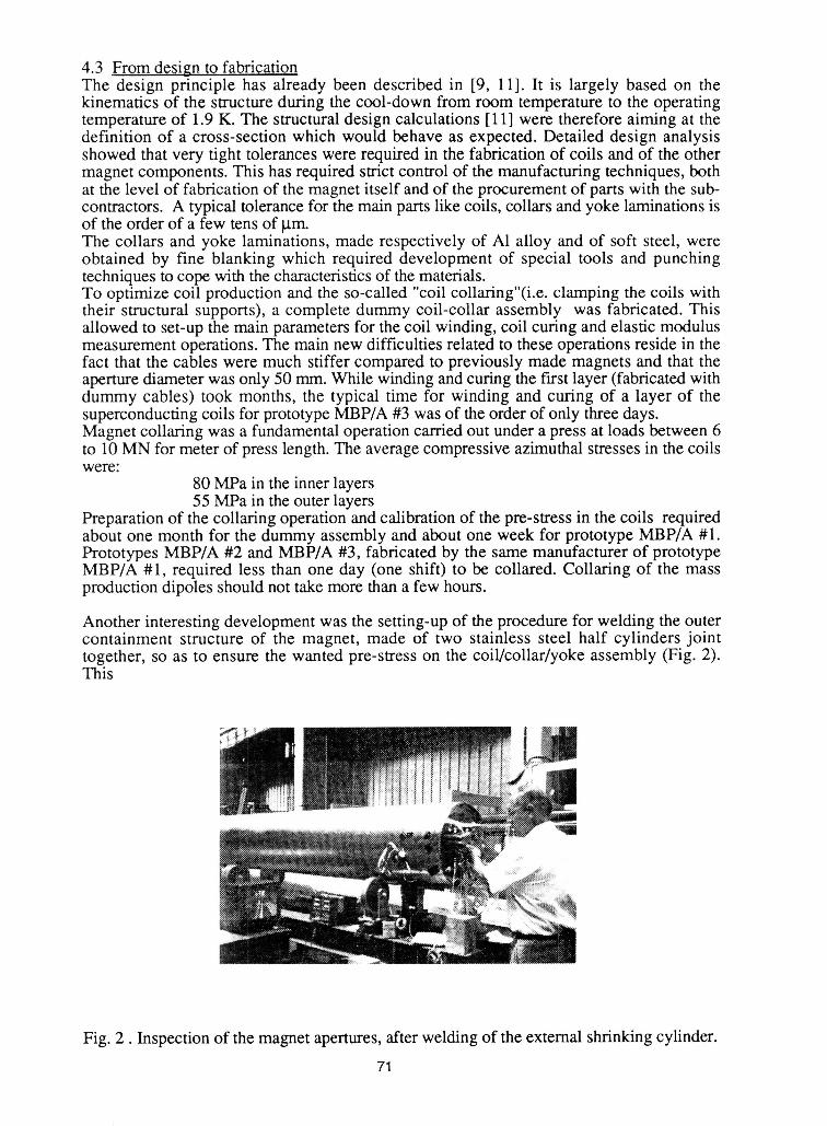
4.3 From design to fabricationThe design principle has already been described in [9, 11]. It is largely based on thekinematics of the structure during the cool-down from room temperature to the operatingtemperature of 1.9 K. The structural design calculations [11] were therefore aiming at thedefinition of a cross-section which would behave as expected. Detailed design analysisshowed that very tight tolerances were required in the fabrication of coils and of the othermagnet components. This has required strict control of the manufacturing techniques, bothat the level of fabrication of the magnet itself and of the procurement of parts with the sub-contractors. A typical tolerance for the main parts like coils, collars and yoke laminations isof the order of a few tens of btm.The collars and yoke laminations, made respectively of A1 alloy and of soft steel, wereobtained by fine blanking which required development of special tools and punchingtechniques to cope with the characteristicsof the materials.To optimize coil production and the so-called "coil collaring"(i.e, clamping the coils withtheir structural supports), a complete dummy coil-collar assembly was fabricated. Thisallowed to set-up the main parameters for the coil winding, coil curing and elastic modulusmeasurement operations. The main new difficulties related to these operations reside in thefact that the cables were much stiffer compared to previously made magnets and that theaperture diameter was only 50 mm. While winding and curing the first layer (fabricated withdummy cables) took months, the typical time for winding and curing of a layer of thesuperconducting coils for prototype MBP/A #3 was of the order of only three days.Magnet collaring was a fundamental operation carried out under a press at loads between 6to 10 MN for meter of press length. The average compressive azimuthal stresses in the coilswere:
80 MPa in the inner layers55 MPa in the outer layers
Preparation of the collaring operation and calibration of the pre-stress in the coils requiredabout one month for the dummy assembly and about one week for prototype MBP/A #1.Prototypes MBP/A #2 and MBP/A #3, fabricated by the same manufacturer of prototypeMBP/A #1, required less than one day (one shift) to be collared. Collaring of the massproduction dipoles should not take more than a few hours.
Another interesting development was the setting-up of the procedure for welding the outercontainment structure of the magnet, made of two stainless steel half cylinders jointtogether, so as to ensure the wanted pre-stress on the coil/collar/yoke assembly (Fig. 2).This
Fig. 2. Inspection of the magnet apertures, after welding of the external shrinking cylinder.
71
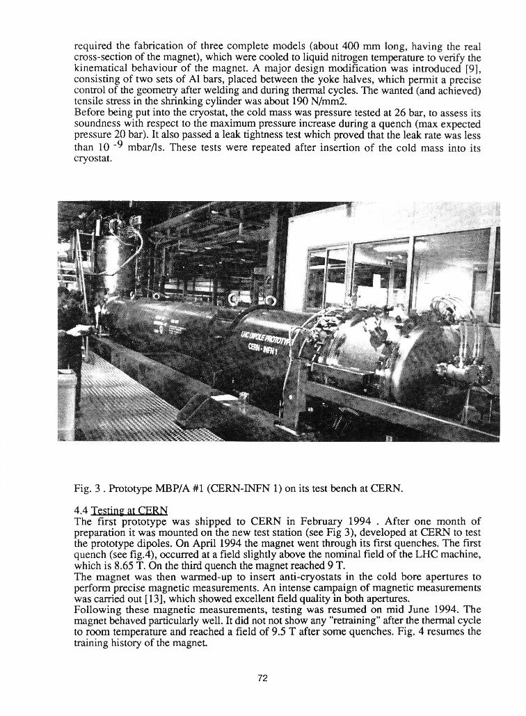
required the fabrication of three complete models (about 400 mm long, having the realcross-section of the magnet), which were cooled to liquid nitrogen temperature to verify thekinematical behaviour of the magnet. A major design modification was introduced [9],consisting of two sets of A1bars, placed between the yoke halves, which permit a precisecontrol of the geometry after welding and during thermalcycles. The wanted (and achieved)tensile stress in the shrinking cylinder was about 190 N/mm2.Before being put into the cryostat, the cold mass was pressure tested at 26 bar, to assess itssoundness with respect to the maximum pressure increase during a quench (max expectedpressure 20 bar). It also passed a leak tightness test which proved that the leak rate was lessthan 10 -9 mbar/ls. These tests were repeated after insertion of the cold mass into itscryostat.
Fig. 3. Prototype MBP/A #1 (CERN-INFN 1) on its test bench at CERN.
4.4 Testing at CERNThe first prototype was shipped to CERN in February 1994 . After one month ofpreparation it was mounted on the new test station (see Fig 3), developed at CERN to testthe prototype dipoles. On April 1994 the magnet went through its first quenches. The f'trstquench (see fig.4), occurred at a field slightly above the nominal field of the LHC machine,which is 8.65 T. On the third quench the magnet reached 9 T.The magnet was then warmed-up to insert anti-cryostats in the cold bore apertures toperform precise magnetic measurements. An intense campaign of magnetic measurementswas carried out [13], which showed excellent field quality in both apertures.Following these magnetic measurements, testing was resumed on mid June 1994. Themagnet behaved particularly well. It did not not show any "retraining" after the thermal cycleto room temperature and reached a field of 9.5 T after some quenches. Fig. 4 resumes thetraining history of the magnet.
72
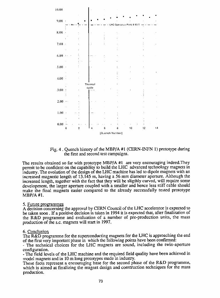
10.00
• m • •
9.00 , • ' " ",-- - _-- ........... LHC Operation Field 865 T .....; t
8.(1(1 -
7,1|0 -
6.00 _ "- -i
5.00 - _ - i
4.00 _
- Thermalcycle
3.00 ............
i
2.00 ......
1.00 - - :
().0_ .......
0 2 4 6 8 10 12 14
[Quench Number]
Fig. 4. Quench history of the MBP/A #1 (CERN-INFN 1) prototype duringthe first and second test campaigns.
The results obtained so far with prototype MBP/A #1 are very encouraging indeed.Theypermit to be confident on the capability to build the LHC advanced technology magnets inindustry. The evolution of the design of the LHC machine has led to dipole magnets with anincreased magnetic length of 13.145 m, having a 56 mm diameter aperture. Although theincreased length, together with the fact that they will be sligthly curved, will require somedevelopment, the larger aperture coupled with a smaller and hence less stiff cable shouldmake the final magnets easier compared to the already successfully tested prototypeMBP/A #1.
5. Future profframme_A decision concerning the approval by CERN Council of the LHC accelerator is expected tobe taken soon. If a positive decision is taken in 1994it is expected that, after finalization ofthe R&D programme and evaluation of a number of pre-production units, the massproduction of the s.c. magnets will start in 1997.
6. ConclusionThe R&D programme for the superconducting magnets for the LHC is approaching the endof the first very important phase in which the following points have been confirmed:- The technical choices for the LHC magnets are sound, including the twin-apertureconfiguration.- The field levels of the LHC machine and the required field quality have been achieved inmodel magnets and in 10 m long prototypes made in industry.These facts represent a encouraging base for the second phase of the R&D programme,which is aimed at finalizing the magnet design and construction techniques for the massproduction.
73
Ackngwlcdgrnen[Several National Institutions and Laboratories have contributed in an important way to thereported R & D work, which received a very substantial support from industry. The LHCMagnet Team gratefully thanks them all.
Reference_:[1] The LHC Study Group, "LHC, The Large Hadron Collider Accelerator Project",
CERN/AC/93(LHC), November 1993.[2] D. Leroy, R. Perin, G. de Rijk, W. Thomi, "Design of a High-field Twin-aperture
S.C. Dipole Model", IEEE Trans. on Magn., vol. 24, March 1988, pp. 1373-76.[3] A. Asner, R. Perin, S. Wenger, F. Zerobin, "First Nb3Sn, 1 m Long
Superconducting Dipole Model Magnets for LHC Break the 10 T Field Threshold",Proc. 1lth Int. Conf. on Magnet Techn., Tsukuba, 1989, pp. 36-41.
[4] R. Ostojic, T.M. Taylor, "Design and Construction of a One-Metre Model of the70 mm Aperture Quadrupole for the LHC Low-b Insertions", presented at MT13,Victoria, Canada, 20-24 September 1993.
[5] M. Bona, D. Leroy, R. Perin, P. Rohmig, B. Szeless, W. Thomi, "Design,Fabrication Variants and Results of LHC Twin-Aperture Models", IEEE Trans. onMagn., vol. 28, pp. 338-341, Jan. 1992.
[6] D. Leroy et al., "Test Results on 10 T LHC Superconducting One-Meter LongDipole Models", IEEE Trans. on Applied Superconductivity, March 1993, vol. 3,No. 1, pp. 614-621.
[7] A. Yamamoto et al., "Development of 10 T Dipole Magnets for the Large HadronCollider", IEEE Trans. on Applied Superconductivity, March 1993, vol. 3, No. 1,pp. 769-772.
[8] M. Granier et al., "Performance of the Twin-Aperture Dipole for the CERN LHC",Proc. EPAC92, Berlin, March 1992.
[9] E. Acerbi, M. Bona, D. Leroy, R. Perin, L. Rossi, "Development and Fabricationof the First 10 Metre Long Superconducting Dipole Prototype for the LHC",presented at MT13, Victoria, Canada, 20-24 September 1993.
[10] J.M. Baze et al., "Design and Fabrication of the Prototype SuperconductingQuadrupole for the CERN LHC Project", IEEE Trans. on Magn., Jan. 1992,vol. 28, pp. 335-337.J.M. Rifflet et al., "Status of the Fabrication and Test of the Prototype LHC LatticeQuadrupole Magnets", presented at MT13, Victoria, Canada, 20-24 September 1993.
[I 1] M. Bona, D. Perini, "Finite Element Structural Analysis of the 10 m Long DipolePrototype Magnet for the LHC", IEEE Trans. on Magn., Vol. 28, Jan. 1992,p. 358. Paper presented at MT12 Conference, Leningrad, June 1991.
[12] J. M. Rifflet et al.,"Cryogenics & Mechanical measurements of the f'u'st two LHClattice quadrupole prototypes", presented at EPAC Conference, London, 27 June-1July, 1994.
[13] M. Bona, D.Leroy, R. Perin, P. Sievers, L.Walckiers, E. Acerbi, L. Rossi,"Results,of tests and measurements of the first CERN-INFN 10 m long superconducting dipoleprototype for the LHC", presented at EPAC Conference, London, 27 June-l July,1994.
[14] R. Perin, "Status Report on the LHC Magnets", presentes at World Congress onSuperconductivity, Munich, Germany, 1991. Applied Superconductivity Vot. 1,Nos 10-12, pp 1487-1502, 1993.
[15] R. Perin, "Status of the Large Hadron Collider", presented at MT13 Conference,Victoria, Canada, 20-24 September 1993.
74
Status of High Temperature Superconductor Development for Accelerator Magnets
H. HirabayashiKEK, National Laboratory for High Energy Physics1-1, Oho, Tsukuba-shi, Ibaraki-ken, Japan 305
1) Abstract
High temperature superconductors are still under development for variousapplications. As far as conductors for magnets are concerned, the development has justbeen started. Small coils wound by silver sheathed Bi-2212 and Bi-2223 oxideconductors have been reported by a few authors.
Essential properties of high Tc superconductors like pinning force, coherentlength, intergrain coupling, weak link, thermal property, AC loss and mechanicalstrength are still not sufficiently understandable.
In this talk, a review is given with comparison between the present achievementand the final requirement for high Tc superconductors, which could be particularlyused in accelerator magnets.
Discussions on how to develop high Tc superconductors for accelerator magnetsare included with key parameters of essential properties.
A proposal is also given how to make a prototype accelerator magnet with highTc superconductors with prospect for future development.
2) Introduction
Since the discovery of superconductivity by K. Onnes in 1911, the record ofcritical temperature (Tc) had been updated slowly by the middle of 1980s. The speed ofupdating the record of Tc was remarkably increased after the discovery of the oxidesuperconductors in 1986, as shown in Figure 1. The highest record of Tc isapproximately 134K for Hg-Ba-Ca-Cu-O1).
The oxide superconductors which have high critical temperatures are generallycalled high Tc superconductors. In recent years, enormous amounts of researchconcentrated on high Tc superconductors all over the world.
In addition to basic studies on superconductivity, various applications to films,tapes and wires have also been intensively studied. However, the high Tc materials arenot well-understood in the viewpoints of solid-state physics and industrial production.
Characteristics of metallic and inter-metallic superconductors, which have lowTc, are also improved continuously. Copper stabilized Nb-Ti wires have becomeapplicable for the magnets in the region of 10T with superfluid helium cooling. A15compound as Nb3Sn copper stabilized superconductor has become also applicable formagnets of 12T at 4.5K with liquid helium cooling.
The superconducting cables commonly used for accelerator dipole andquadrupole magnets in the range of several teslas are Nb-Ti Copper cables andpractically operated at 4.5K with liquid helium cooling. Some magnets are wound withcopper stabilized Nb3Sn wires for actual operation around 12T at 4.5K. Nevertheless, itis difficult to use these wires and cables in the operation beyond 15T.
Recently, it was found that some oxide superconductors are applicable up to 30Tat 4.2K2)as shown in Figure 2. This is quite attractive in application to generate a veryhigh magnetic field.
75
Figure 3 shows the Tc of the metallic and the oxide superconductors. A15intermetallic compound superconductor shows intermediate values between those ofmetallic and oxide superconductors in Tc and Hc.
3) Present status of high T,: superconducting wires and cables
There are three types of high Tc superconducting wires and cables, e.g., Bi-, Y-and Tl-based materials. Among these materials, Bi-based ones are considered as a mainstream of development. Specially, Bi-2223 and Bi-2212 are studied by manyresearchers.
Bi-based silver sheathed Bi-2223 and Bi-2212 have been remarkably developedas the high Tc wires and cables for magnets.
G. J. Yurek has manufactured multi-core, tape-shaped wires using a combinationof the metallic precursor method, and the silver-sheath method3) and the technique toproduce about 300m long wires has been established. The wire Jc is reported to bearound 50A/mm2 at 20K in 5T for 3m long wires, and Jc=37A and 24A at 77K in 0Tfor 30m and 300m long cables, respectively.
P. Haldar et al., reported the results of the test of short samples at 4.2K, 27K and77K under magnetic fields up to 20T.4)
Quite recently, T. Hikata et al., reported the result of lkm-class silver-sheathedBi-based superconducting wires. 5) They made monofilamentary and 61-multifilamentary wires. A Jc of 40A/mm2 was achieved for 1,080m long wire. Ananisotropy for the direction of external magnetic fields was found in Jc. They measuredthe parameter (Jcxlength). The maximum value was (Jc×length)=9.91×10¹⁰[A/m] for623m long wire. Figure 4 shows the 1080m long high Tc tape wound in a coil.
Pancake coils wound with high Tc wires and cables were studied by S.Meguro. 6) He studied the temperature dependence of Jc of Bi-2212 wire in magneticfields and showed the possibility to operate the Jelly Rolled Bi-2212 silver sheathedsuperconductor below 20K.
Among high Tc superconductors available at present, it seems, only Bi-basedsilver sheathed conductors have suitable characteristics for accelerator magnetapplication. Bi-2212 silver sheathed tapes were significantly improved in Jc with theformation of the high c-axis orientation of laminated grains and reached Jc = 350A/mm2
at 77K with zero external magnetic field. However, Jc was lowered down to -- 4A/mm2at the same temperature with an external field of IT. The large magnetic fielddependence is not suitable for accelerator magnet application at 77K. Further study isnecessary to find the method to satisfy both requirements of high Jc and Ic.
On the other hand, this highly c-axis oriented Bi-2212 high Tc superconductingtape could survive since it shows high Jc = 20A/mm2with the external magnetic field ashigh as 30T, if it is cooled down to 4.2K.
The Jc of high Tc superconductor around several tesla is still much lower thanthat of metallic superconductors which are presently used as accelerator magnets.
4) Requirements for superconducting wires and cables of accelerator magnets
The advantage of using high Tc materials for accelerator magnets is that therefrigeration system for high Tc magnets is much simpler than that for conventionalmetallic superconducting magnets. Quench protection from the heat load due to beamradiation is also expected to be easier.
76
The requirements for accelerator magnets are complicated since they must bedetermined after a delicate adjustment of various parameters which are not alwayscompatible with one another. We discuss an overview of common requirements for10T-class superconducting magnets which are desirable for a multi-TeV accelerator.
The beam size of the accelerator is preferred to be as small as reasonablyachievable by optimizing the beam optics and improving a beam cooling technique,since the costs have risen remarkably for large scale magnets. A small magnet for ahigh field requires a high current density. The current density of 400A/mm 2 in thewindings is a reasonable goal, which requires the current density of more than1000A/mm2 in the wires. This implies that the electric insulation must endure 100-150MPa at low temperatures. The choice of insulation materials and the manufacturingtechnique must be improved to achieve these conditions.
5) Proposed high Tc superconducting accelerator magnet cables
As mentioned in the previous section, requirements for superconducting wiresand cables of accelerator magnets are remarkably severe. Further improvement isnecessary for the production of high Tc superconductors for this application.
A possible solution to apply high Tc superconducting wires for acceleratormagnets is to make a so-called superferric magnet as shown in Figure 5. In thisconfiguration, the superconducting coil is cooled down together with the magnetic ironand enables us to assemble accelerator magnets below 2T. However, wires and cablesare required to have much more mechanical strength and much better performance forthe application to accelerator magnets which can be operated in the magnetic fieldlarger than 2T, e.g. 5 to 10T.
One possible way to develop such wires and cables with high Tcsuperconductors is to combine the longitudinal in-situ and radial Jelly Rolled structuresof the wire strands. The longitudinal in-situ structure within the coherent length ofpolycrystals in metallic wire will improve the Jc along the wire length and the Jelly Rollwill also improve the Jc deterioration with external magnetic field. We believe that sucha structure of high Tc superconducting wires should be created and tested for the futureapplication to accelerator magnet.
6) Conclusions
Superconductingacceleratormagnetsrequirehigh Tccableswhichshowa highJc andIc witha strongmagneticfield.
A proposed solution for these requirements is to develop the Jelly-Rolled Bi-2212 silver sheathed round wires. The multi-layer and round shape cross-sectionalstructure could be another solution for high Jc and Ic requirements. The Jccharacteristics of this type of wires will be heavily deteriorated above 20K, therefore itis suitable for magnet operation at temperatures below 20K.
Another solution to develop accelerator magnet wire and cable would be foundin a further study of the in-situ structure in high Tc polycrystal superconductors byadjusting their coherent length in appropriate metallic sheaths and/or stabilizers.
From the viewpoint of accelerator magnet application, we expect thedevelopment of high Tc superconducting wire with high Jc, Ic and lengths over 1 km innear future.
77
It is still very hard to see how high-Tc superconducting wires could be operatedwith high-Jc and high-Ic at the temperature around 70K. Further study of high Tcsuperconductors are strongly desired.
7)Ackn0wledgments
The author is grateful to Drs. K. Sato of SEI and S. Meguro of FEC for theirkind suggestions. He is also grateful to staff members of Cryogenics Center of KEKfor the preparation of this paper.
8)References1) A. Schilling et al., Nature 363, 56(1993).2) M. Mimura et al., Advances in Superconductivity V, eds. Y. Bando and H.
Yamauchi, Springer-Verlag (ISS'92), p.693-696, and private communication.3) G. J. Yurek, Advances in Superconductivity VI, eds. T. Fujita and Y. Shiohara,
Springer-Verlag (ISS'93), p.3-8.4) P. Haldar et al., Advances in Superconductivity VI, eds. T. Fujita and Y.
Shiohara, Springer-Verlag (ISS'93), p.605-608.5) T. Hikata et al., Proceedings of the 1994 International Workshop on
Superconductivity, Jun. 6-9, 1994, Kyoto, Japan, p.69.6) S. Meguro, private communication.
78
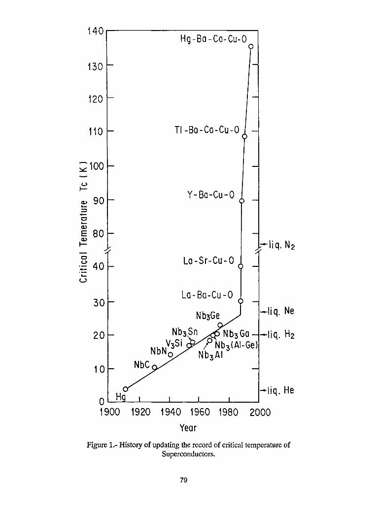
140Hg-Bo-Ca-Cu-O
130 -
120 -
110 - TI-Ba-Co-Cu-O
-,-liq.He0 Hg I _ i i1900 1920 t94.0 1960 1980 2000
Year
Figure 1.- History of updatingthe record of critical temperature ofSuperconductors.
79
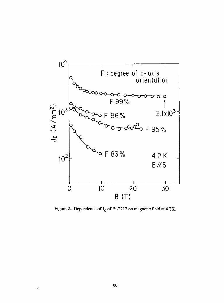
0 I I I
F" degreeof c- axis
F99% I103
E F 96 % 2.1x10³
F 95%
102_ -oF 83% 4.2K _B//S
I I I
0 10 2O 30B (T)
Figure 2.- Dependence of Jc of Bi-2212 on magnetic field at 4.2K.
80
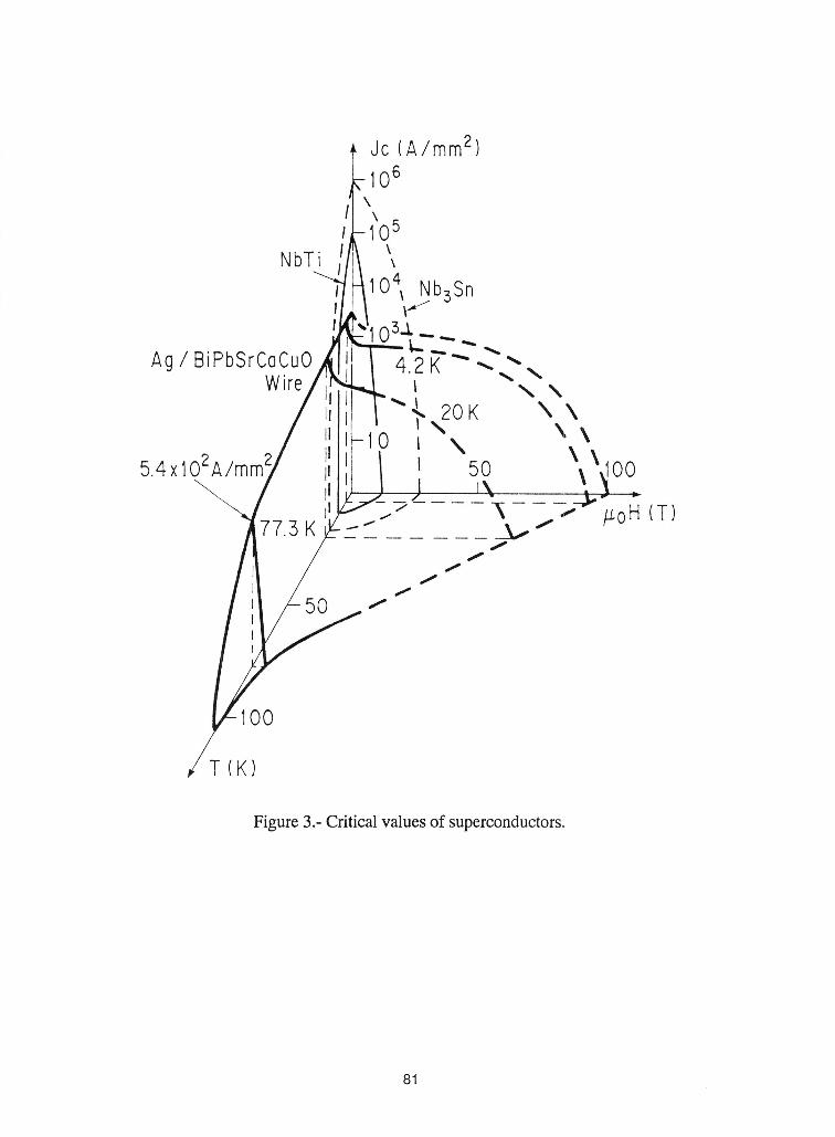
_T 100(K)
Figure 3.- Criticalvalues of superconductors.
81
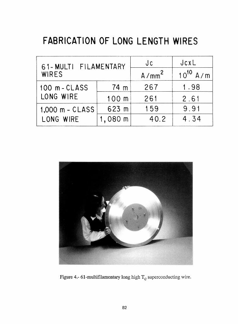
FABRICATIONOFLONGLENGTHWIRES
61- MULTI FILAMENTARY Jc JcxLWIRES A/mm2 10l° Aim
100 m-CLASS 74 m 267 1.98LONGWIRE 1O0 m 261 2.61
1,000m- CLASS 623 m 159 9.91LONGWIRE 1,080 m 40.2 4..54
Figure 4.- 61-multifilamentary long high Tc superconductingwire.
82
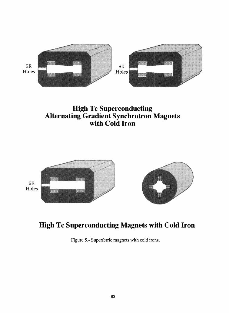
SR SRHoles Holes
High Tc SuperconductingAlternating Gradient Synchrotron Magnets
with Cold Iron
SRHoles
High Tc Superconducting Magnets with Cold Iron
Figure 5.- Superferricmagnetswith cold irons.
83
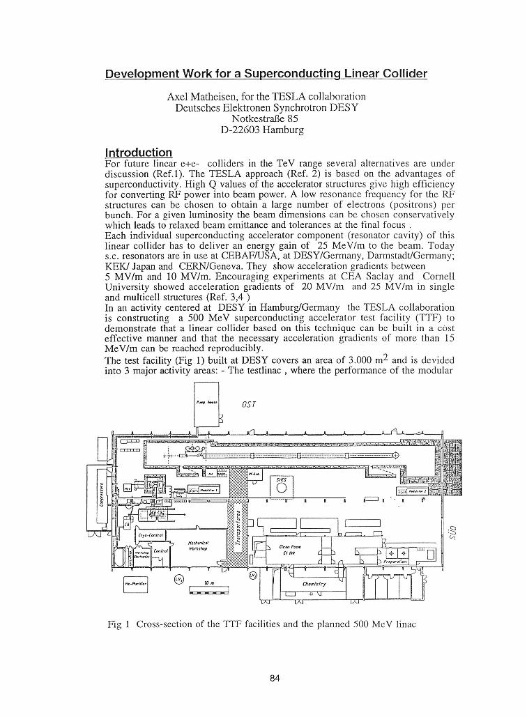
DevelopmentWork for a SuperconductingLinear Collider
Axel Matheisen, for the TESLA collaborationDeutsches Elektronen Synchrotron DESY
Notkestral3e 85D-22603 Hamburg
IntroductionFor future linear e+e- colliders in the TeV range several alternatives are underdiscussion (Ref.1). The TESLA approach (Ref. 2) is based on the advantages ofsuperconductivity. High Q values of the accelerator structures give high efficiencyfor converting RF power into beam power. A low resonance frequency for the RFstructures can be chosen to obtain a large number of electrons (positrons) perbunch. For a given luminosity the beam dimensions can be chosen conservativelywhich leads to relaxed beam emittance and tolerances at the final focus.Each individual superconducting accelerator component (resonator cavity) of thislinear collider has to deliver an energy gain of 25 MeV/m to the beam. Todays.c. resonators are in use at CEBAF/USA, at DESY/Germany, Darmstadt/Germany;KEK/Japan and CERN/Geneva. They show acceleration gradients between5 MV/m and 10 MWm. Encouraging experiments at CEA Saclay and CornellUniversity showed acceleration gradients of 20 MV/m and 25 MV/m in singleand multicell structures (Ref. 3,4 )In an activity centered at DESY in Hamburg/Germany the TESLA collaborationis constructing a 500 MeV superconducting accelerator test facility (TTF) todemonstrate that a linear collider based on this technique can be built in a costeffective manner and that the necessary acceleration gradients of more than 15MeV/m can be reached reproducibly.The test facility (Fig 1) built at DESY covers an area of 3.000 m2 and is devidedinto 3 major activity areas: - The testlinac, where the performance of the modular
Fig 1 Cross-section of the TTF facilities and the planned 500 MeV linac
84
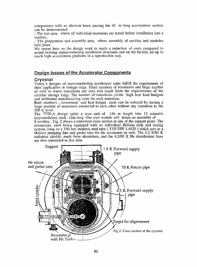
components with an electron beam passing the 40 m long acceleration sectioncan be demonstrated.- The test area, where all individual resonators are tested before installation into amodule.- The preparation and assembly area, where assembly of cavities and modulestake place.We report here on the design work to reach a reduction of costs compared toactual existing superconducting accelerator structures and on the facility set up toreach high acceleration gradients in a reproducible way.
Design Issues of the Accelerator Components
CryostatToday's designs of superconducting accelerator units fulfill the requirement oftheir application in storage rings. Small numbers of resonators and large numberof cold to warm transitions per cryo unit result from the requirements of thecircular storage rings. The number of transitions yields high heat load budgetsand additional manufacturing costs for each transition.Both numbers , investment- und heat budget costs can be reduced by having alarge number of resonators connected to each other without any transition to the300 K level.The TESLA design splits a cryo unit of 144 m length into 12 subunits(cryomodules), each 12m long. One cryo module will house an assembly of8 cavities. Fig. 2 shows a transverse cross section at one of the support posts. Theresonators, each being equipped with its individual Helium tank and tuningsystem, hang on a 350 mm stainless steel tube ( TYP DIN 1.4429 ) which acts as aHelium pumping line and girder tube for the resonators as well. The 4.2 K/80 Kradiation shields, made from aluminium, and the 4.2180 K He distribution linesare also connected to this tube.
Support 1.8 K Forward supplypipe
He returnand girder tube 70 K Return pipe
/
=_/ 41.5 K Forward supply8i pipe
for aligenement
Fig 2. Cross section of the cryostatResonatorZwith He Tank
85
Three posts, made from carbon fiber, take the gravitational forces of the girdertube to the rigid vacuum vessel made from carbon steel . For this design thestatic heat loss at 1.9 K is calculated to be 0.4 W/m. This will be a reduction by afactor of ten compared to the actual existing storage ring designs.
CavityBesides the increase of acceleration gradients cost reduction during fabrication isneeded in order to make s.c.cavities a competitive alternative to warm structures.A large amount of cost intensive manufacturing is related to the auxiliaries likepower input couplers, higher order mode (HOM) damping couplers and tunersconnected to each cavity. A compromise between reduced costs by an increasednumber of cells per cavity, the excitation of higher order modes and the
appearance of trapped modes has to be made. _ l_- _N;_- !/
..................................................................N-:.................!.....
.t__Jt_ , .1 ?_==
• . _M! I I_----_
---_ '_:'-'.'. ...;; _ '£'t............._...... -_
Fig.3Longitudinalcrosssectionof theTESLAresonatorcoveredby theHetank
The TESLA resonator (Fig. 3 ) is built from 9 cells with an eigenfrequency of1.3 GHz .The RF power is fed in by the inputcoupler, perpendicular to the beam axis, while theHOM modes are damped by two couplers on eachside of the cavity. The geometry of this resonator t _300[MHzI
results in the numbers listed in Table 1. The tO4Ol lo3oI_lresonators will be made from high thermalconducting 2.8 mm thick niobium sheet material Ep_I z(RRR >300) by deep drawing and electron beam
Hp/EaC 42.2 [GstMVIm Iwelding technique. To reduce the number of cost-intensive welds, new technologies are investigated in k _.87addition.The HOM couplers are extruded in one stepfrom a Nb pallet to their final shape, while the beam ___ .7 IMHzl
pipes are machined from sheet material by spinning. _o,g.Using these technologis a total number of 5 welds =o_K 9.z_[v/pcland several intermediate production steps likechemical etching and calibration are eliminated.Further investigations on seamless cells and resonatorsare made in the collaboration. Table 1. TESLA
cavity parameters
TuningFor an optimized energy transfer to the beam, all resonators have to have theresonance frequency within an accuracy of some Hz. Room temperatureadjustment errors result in frequency variations of +-200kHz. To ajust the staticfrequency shift slow reacting tuners are installed in the vacuum at the 80 K level.A lever arm system driven by a stepping motor via an elliptical gearbox acts on
86
the cavity. By elongation and contraction of the structure this arangement allows afrequency adjustment of +- 4 HzElectromagnetic forces act on the resonator surface during RF pulses. Due tothese Lorentz forces, a fast displacement of the walls ( 10-4 mm at Eacc = 25MV/m) will occur at every RF pulse . This displacement results in a frequencyshift of 1.2 kHz to be compared with a bandwidth of the loaded cavity of 360 Hz.Stiffening rings between each cell reduce this fast displacement down to afrequency shift of 600 Hz (360 Hz by the cavity +300 Hz by the tank), which willbe tolerable for the RF system.
Power couplerThe RF power transferred to the beam will be 200 KW/cavity in pulses of 2 mseclength with a repetition rate of 10 Hz. Sixteen cavities are driven in parallel byone 4.5 MW klystron. Besides the power transfer the input power coupler has toseparate the resonator vacuum of 10-10 mbar at 1.8 K and the atmosphericpressure at 300 K. Two ceramic windows, as shown in Fig. 4, are integrated, oneat a temperature level of 80 K, to separate the clean cavity vacuum from theinsulation vacuum and the second at room temperature for the
7Fig.4Crosssectionof an inputcoupler(DESYType)
transition to atmospheric pressure. The separation of the vacua allows a dust freeassembly and sealing of the resonator in the cleanroom independently from theassembly of the coupler in the cryomodule .The heat loads introduced to the1.8 K and 4.2 K level by this coupler will be 0.61 W for static- plus dynamiclosses. T_
HOM Couplers I demo_X_,=_ap=iTwo different designs of HOMcouplers are studied. Fig.5shows the coaxial type couplerdesign which is fixed to thebeam pipes by EB welding. Thefish hook coupler designflanged to the beampipe isshown in Fig. 2 . These twoversions have to be compared inrespect to costs, handling andreliability. Fig.5DemountableHOMcoupler
87
Infrastructure
Experimental HallThe TESLA Test Facility is located in an experimental hall of about 3.000 m2ground area (see Fig. 1). Half of this space will be occupied by the test linacdescribed later.The second part of the hall is supplied with equipment for tests,assembly and surface treatment of all linac components. The most importantcomponents of this infrastructure are a cleanroom and the surface treatment area,which cover 1/4 of the space.
1.8 K test areaTo reduce dynamic losses due to BCS surface resistance, the resonators will becooled down to 1.8 K . The necessary cooling is supplied by a refrigerator of200 W cooling power at 1.8 K.To test and qualify the resonators before insertion in the cryomodule, three testcryostats are installed. Two vertical dewars for tests of resonators not equippedwith the helium tank allow RF processing of resonator defects by high peak powerprocessing (HPP). In case of appearance of defects, limiting a single resonatorbelow the goal of 20 MWm, a surface temperature mapping setup can be attachedto the cavity in order to Studyand localize the limitation.The two clystrons for supplying the testlinac with RF power are located next to thecold test area. The power distribution system of one klystron allows to feed eachtest cryostat with pulses of 2 MW power for HPP of resonators.
Cleanroom and assembly areaThe most important components of the TTF infrastructure are a cleanroomincluding an ultra pure water supply, a chemical etching facility and a furnace forpostpurification of niobium.In order to reach the necessary cleanliness for high gradient resonators, thestandards of electronic industry are applied in a cleanroom of 300 m2 space(Fig.6). A class 100 ASTM area of 100 m2 space is installed to assembleindividual cavities and align the resonators to a cryomodule string under dustfree conditions. Inside this cleanroom 2*20 m2 of class 10 ASTM are installedfor assembly of critical components connected to the resonators. Access to thisarea is provided by the sluices for personal and material separately.These sluicesare equipped with ionized air guns for cleaning and particle counters formonitoring. In the class 10.000 area a separate space of 70 m2 is used for highquality surface cleaning and treatment (chemistry area).
'"'[-1
IL.,M[_: Cl_lO.O00chem:strya_ LAJ _ ! __ ] L_10m
Fig 6. Cross section of the cleanroom area
88
Ultra pure water and ultra pure nitrogen gas lines,coming from separate plants,are connected to this area. An ultrasonic bath of 400 1capacity, a rinsing basin of400 1capacity as well, a preparation area and a high pressure rinsing cabinet allowto clean the cavities and handle all sophisticated parts which have to be adopted tothe resonators during final assembly. Remote controlled oil free pumping stationsare located outside the cleanroom to establish the vacuum and leak checks underdust free conditions.
ChemistryInside the chemistry area a cabinet for surfacetreatment by etching of the niobium is installed.The acid in use is a chemical mixture of HF/HNO3/H3PO4 (*1) in a 1/1/2 volume mixture. The acid iscirculating in a closed loop between the storagetanks and the cavity. The storage tanks are locatedin a separate area outside the cleanroom . Thepumps, pumping lines (made from PVDF) andfilter elements ( 0.2 _tm size) of the chemistrydistribution system fulfill the standards of theelectronic industry.Two different acid treatments are foreseen. Theoutside treatment removes the niobium-titaniumsurface layer after the postpurification of theniobium in the furnance whereas the insidetreatment with highest quality requirements is usedfor the preparation of the inner RF surface.Theseparation of the two treatments is guarantieed bytwo independent piping circuits in the chemistrydistribution system. In addition, separate cabinetsfor supply and disposal of acid are installed.The temperature of the acid can be set between5 C° and 20 C° with a massflow up to 20 1/min.The process and the safety interlocks are controlledby a computer to reach high safety andreproducibilty standards. After the etching process Ithe cleaning procedure is finished by an ultrapure I Iwater rinse and drying in an ultra clean nitrogen z Iatmosphere. ! II I
Ultra pure waterAn ultra pure water plant (UPW) supplies theprocesses with water of L= 18.2 MffZcm underparticle free conditions .The UPW circuit isequipped with reverse osmosis precleaning, apolisher stand with two mixed bed ion exchangers,point of use particle filters and ultra violet lightsource to avoid bacteria contamination. Apermanent circulation in the pipes, the storage tankand the filters via a separate feedback line providesa minimization of existing death volumina. Thestorage tank of 4.000 1 capacity allows to dischargelarge quantities of the ultra pure water in short timeperiodes. The quality of the water is perma- Fig.:8Cross section of the high
pressurerimingstation
89
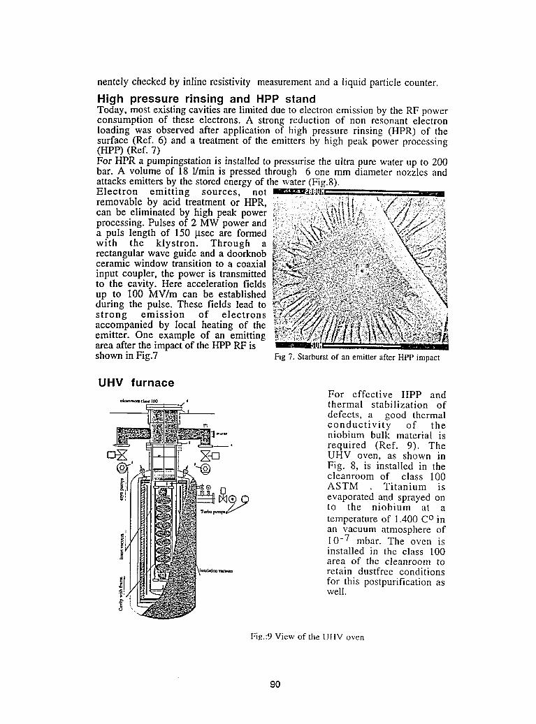
nentely checked by inline resistivity measurement and a liquid particle counter.
High pressure rinsing and HPP standToday, most existing cavities are limited due to electron emission by the RF powerconsumption of these electrons. A strong reduction of non resonant electronloading was observed after application of high pressure rinsing (HPR) of thesurface (Ref. 6) and a treatment of the emitters by high peak power processing(HPP) (Ref. 7)For HPR a pumpingstation is installed to pressurise the ultra pure water up to 200bar. A volume of 18 1/min is pressed through 6 one mm diameter nozzles andattacks emitters by the stored energy of the water (Fig.8).Electron emitting sources, not _m_t_I,:111;, ,
removable by acid treatment or HPR, i:i;::: _ (ff:_
can be eliminated by high peak power _ iprocessing. Pulses of 2 MW power and i:i::i,:!_:_-_ _;_:_,_._i_i_i_;a puls length of 150 gsec are formed _i:i:i::2.iii_:ili_!_!_;_}2_i_)iwith the klystron. Through a _%,__:_,_:;_>-;_::_,_:_,_.:_.......rectangular wave guide and a doorknob r_:,:,_:_,_,:-.;;_,,,_,_o,:_,_,-_ceramic window transition to a coaxial ,_!:_:y,2_:_;_s_7:r:-,_7 _;_;,input coupler, the power is transmitted ,,_::_:,,-_,yx_,,_+_:_:_:::_,_:,:.:,._,,to the cavity. Here acceleration fields 7:_+t',,#_>,_:_:;::_;::,_:_;_;:+_"up to 100 MV/m can be established g#_:_._:_k',:_'-_:,;_._--';_:-:*_:during the pulse. These fields lead to _:_/:_'._>_,,,._,._.._:_:'sstrong emission of electrons _":::_:"'°''_'_:_--_:_';-_'_ _"accompanied by local heating of the
emitter. One example of an emitting _;iSi_i,_i::_i.:_,:area after the impact of the HPP RF isshown in Fig.7 Fig 7. Starburst of an emitter after HPP impact
UHV furnaceFor effective HPP and
""'-'_'® ' thermal stabilization ofdefects, a good thermal
r_ conductivity of theniobium bulk material isrequired (Ref. 9). The
_23 UHV oven, as shown in'--@ Fig. 8, is installed in thecleanroom of class 100
ASTM Titanium is_[ evaporated and sprayed on
to the niobium at atemperature of 1.400 C° inan vacuum atmosphere of10 -7 mbar. The oven isinstalled in the class 100area of the cleanroom toretain dustfree conditionsfor this postpurification as
-_ well.
Fig.:9 View of the UHV oven
9O
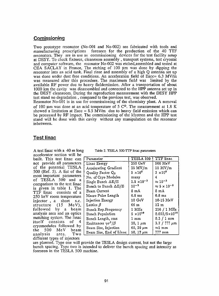
Comissioninq
Two prototype resonator (No-001 and No-002) are fabricated with tools andmanufacturing prescriptions foreseen for the production of the 40 TTFresonators. They are in use as commissioning devices for the test facility setupat DESY. To check fixtures, cleanroom assembly, transport systems, test cryostatand computer software, the resonator No-002 was etched,assembled and tested atCEA SACLAY in France, The etching of 100 lxm was done by dipping theresonator into an acid tank. Final rinse and assembly of a high Q antenna set upwas done under dust free conditions. An acceleration field of Eacc= 6.3 MV/mwas measured after this procedure. The maximum field was limited by theavailable RF power due to heavy fieldemission. After a transportation of about1000 km the cavity was disassembled and connected to the HPP antenna set up inthe DESY cleanroom. During the reproduction measurement with the DESY HPPtest stand no degradation, compared to the previous test, was observed.Resonator No-001 is in use for commissioning of the chemistry plant. A removalof 100 _tm was done at an acid temperature of 5 C°. The measurement at 1.8 Kshowed a limitation at Eacc = 8.5 MV/m due to heavy field emission which canbe processed by RF impact. The commissioning of the klystron and the HPP teststand will be done with this cavity without any manipulation on the resonatorinbetween.
Test linac
A test linac with a 40 m long Table 2. TESLA 500-TrF linac parametersaccelerator section will bebuilt. This test linac can Parameter TESLA 500 TTF linacnot provide all parameters Linac Energy 250 GeV 500 MeVof the potential TESLA AcceleratingGradient 25 MV/m 15 MV/m500 (Ref. 5). A list of the QualityFactor Qo 5 xl09 3 xl09most important parameters No. of CryoModules many 4of TESLA 500 and acomparison to the test linac SingleBunchAE/E 1.5 ×10⁻³ _ 10 -3is given in table 1. The Bunch to Bunch AE/E 10-3 _ 5 x 10⁻³TTF linac consists of a BeamCurrent 8 mA 8 mA250 keV room temperature Maao Pulse Length 0.8 ms 0.8 msinjector , a short s.c. InjectionEnergy I0 GeV I0-15 h(eVstructure (15 MeV), Latticefl 66 m 12 mfollowed by a beam BunchRep.F_equency 1 MHz 216 / 1 MHzanalysis area and an optics BunchPopulation 5 x 101° 0.023/5 x 10_°matching system. The linac BunchLength, rms 1 mm 0.3 / 1 mmitself consists of 4 Emittances 7o':/fl 20, 1/zm 3.7 / ???/lmcryomodules followed bythe 500 MeV beam Beam Size, Injection 60, 20/zm _1 mm
analysis area. Two Beam Size, End of Linac 50, 12/zm ??? mmdifferent types of injectorsare planned. Type one will provide the TESLA design current, but not the largebunch spacing. Type two is intended to deliver the bunch spacing and intensity asforeseen in the TESLA 500 machine.
91
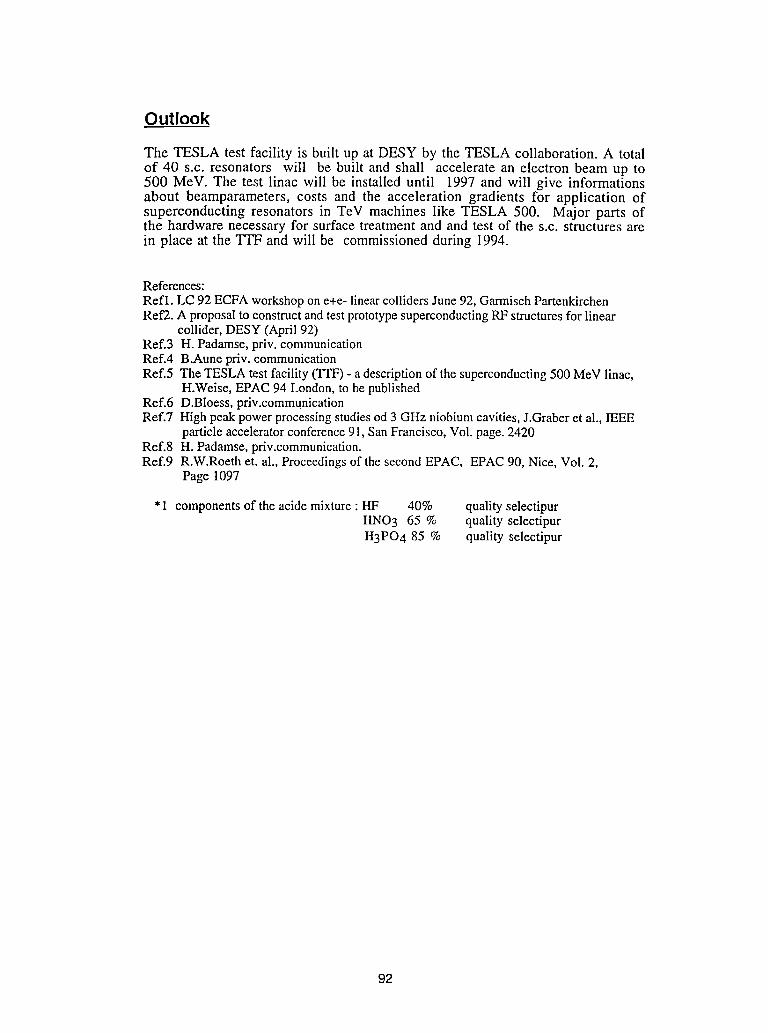
Outlook
The TESLA test facility is built up at DESY by the TESLA collaboration. A totalof 40 s.c. resonators will be built and shall accelerate an electron beam up to500 MeV. The test linac will be installed until 1997 and will give informationsabout beamparameters, costs and the acceleration gradients for application ofsuperconducting resonators in TeV machines like TESLA 500. Major parts ofthe hardware necessary for surface treatment and and test of the s.c. structures arein place at the TTF and will be commissioned during 1994.
References:Refl. LC 92 ECFA workshop on e+e- linearcolliders June 92, Gannisch PartenkirchenRet'2. A proposal to construct and testprototype superconducting RF structures for linear
collider, DESY (April 92)Ref.3 H. Padamse, priv. communicationRef.4 B.Aune priv. communicationRef.5 The TESLA test facility (TTF) - a description of the superconducting 500 MeV linac,
H.Weise, EPAC 94 London, to be publishedRef.6 D.Bloess, priv.communicationRef.7 High peak power processing studiesod 3 GHz niobium cavities, J.Graber et al., IEEE
particle accelerator conference 91, San Francisco, Vol. page. 2420Ref.8 H. Padamse, priv.communication.Ref.9 R.W.Roeth et. al., Proceedings of the second EPAC, EPAC 90, Nice, Vol. 2,
Page 1097
*1 components of the acide mixture : HF 40% quality selectipurHNO3 65 % quality selectipurH3PO4 85 % quality selectipur
92

THIS PAGE INTENTIONALLY LEFT BLANK


Power and Energy
Chair: Prof. Istvan Kirschner
Today's Research Developmenton the Applicationof
the SuperconductivityTransportSystem in Japan
Yoshihiro KyotaniTECHNOVA Inc.
Tokyo Japan
Abstract
At the Miyazaki test track today, thenew test vehicle,MLU002N,is under test run to
obtain necessarydata for Yamanashitest track wherethe constructionis underway,the
test vehiclehas been orderedand thef'ast tunnel was completedin December' 93.
Superconductingmagnetohydrodynamicdrive ship,MHDS,"Yamato 1"has
completed its experimentin '92 and it is now underpreparationto exhibit to the public
in '94. Furthermore, to promote theresearchdevelopmentof MHDS, the detailed
discussion is underway on the magnetohydrodynamicdrive equipmentas well as theresearch on the future scheme.
Neitheran automobilenor railwaybut a new transportsystem calledEQUOS LIM
CAR(ELC) has been proposed.By using therotating magneticfield, it will levitate on
the aluminumlike reactionplate. On thenormalroad, it will run by rolling the wheels
like an electriccar but on the highway,it will levitateon the guidewayresulting to less
noise, less vibration and pollution free drive.To understandthe concept of the ELC,
the model was built and experimentedby usingpermanentmagnet.The same model
was donated to the MUSEUMOF SCIENCEAND INDUSTRYin Chicago and was
displayed to the public.Today, the trial superconductingmagnet has been made and the
research developmentof the subsystemis underway.
Researchdevelopmentof superconductingelevator,equipmentfor the launchingof
spaceship, tube transportationsystem and others are in progress for the
superconductingapplied transportationsystem.
SUPERCONDUCTINGMAGNETICALLYLEVITATEDRAILWAY
Today in Japan, under the supervisionof the Ministryof Transportationand with the
cooperationof universities and enterprises,CentralJapan Railway Company,Japan
RailwayconstructionCorporationand RailwayTechnicalResearchInstituteare
promoting thedevelopmentof the SuperconductingMagneticallyLevitated Railway,
hereundercalled SG-Maglev.
Eachconcemedare aimingas an immediateobjectiveto completetheYamanashiTest
Track. On the other hand, at, MiyazakiTest Track,experimentsareprogressed by
Railway Technical ResearchInstituteto obtainnecessaryinformationfor YamanashiTest Track.
96
In September,'93, Symposiumon' 93 CentralSuperExpresson the RailwayAcademicConferencewasheldatYokohamawitha themeof "CentralSuperExpressand Community".
MiyazakiTestTrack:In December '79, 10meters long weighing 10tons of test car,
ML500, has recorded a high speed of 517 km/h at the Miyazaki test track. With this
test, passengers loadable test car, MLU001with 3 carriage cars,were trialmanufactured.
By using MLU001, it has been confm'nedthat the travel stabilitywill increase when
the connection cars are added and also travelingcharacteristicswere obtained. In
September '82, manned testing run has started. Then in February '87, after increasing
the capacity of electric power supply facilities, I was onboard on the 2 carriage car and
reached the high speed of 401 km/h.
In March '87, to promote more practical use of test car, MLU002 was completed and
exhibited to the domestic and internationalrelatedmedia by Japan National
Railways(JNR). In November '89, it has reached the high speed of 394 km/h.
In the case of MLU001, superconductingcoils are placed equally in chain under the
car while with MLU002, superconductingcoils areconcentrated under the front and
back edge of the car. In considering the concept of the commercial cars, this was due to
reduce the air resistance and the magneticfield effect to the passengers. On the other
hand, instead of placing levitate coils on the running track of the guideway as an
opposite direction levitation, the researchon placing levitatecoils at the side of the wall
levitate method is under study.
Not only of the concentratedplacement but also to stimulatethe test of the side walllevitate method test started in June '91. As a result, the blockof side wall levitate
method was further extended to obtain necessary informationfor the Yamanashi test
track but in October, same year, MLU002had a fire accidentand became inapplicable.
The f'u'eaccident of MLU002 was a regret but with the effort of the people concerned
and the enthusiasm of many peoplerelated to the materializationof SC-Maglev, the new
MLU002N was manufactured and started its test from January '93. MLU002N has a
length of 22m, width 3m and weighs 19tons. In February '94, MLU002N has
recorded high speed of 431 km/h at Miyazaki test track.
97
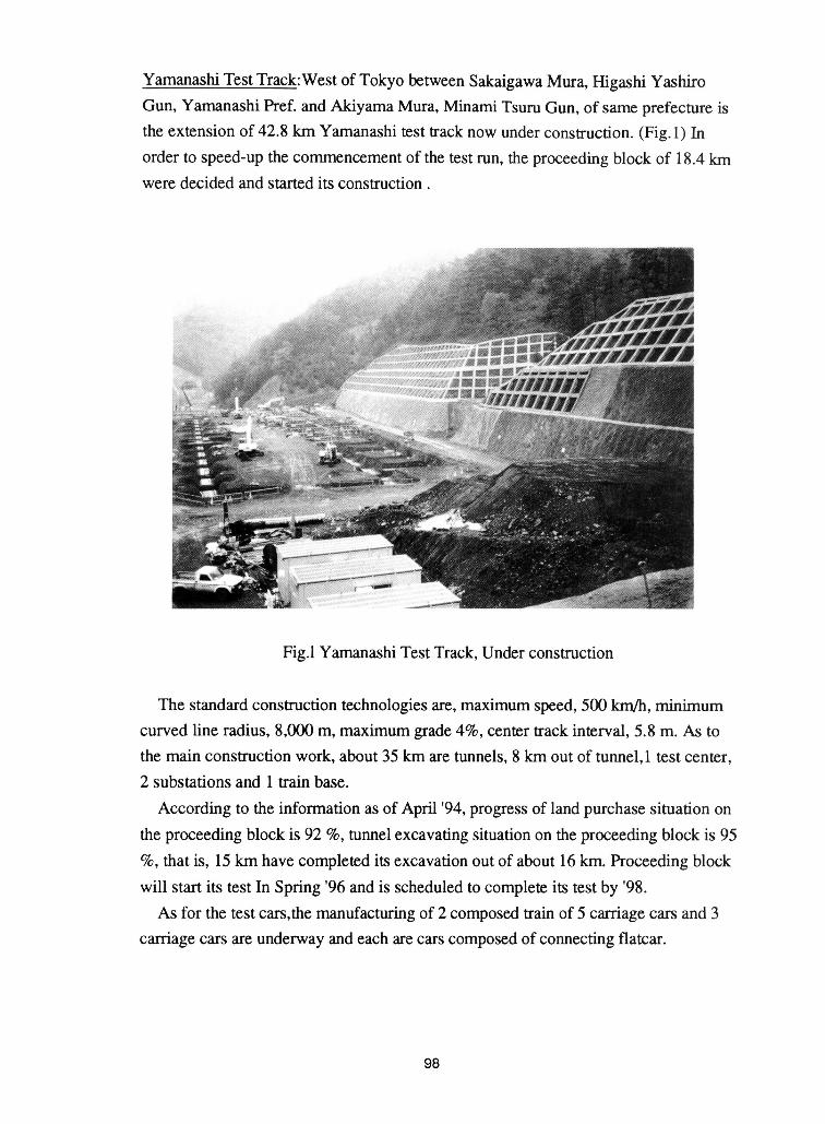
Yamanashi Test Track:West of Tokyo between Sakaigawa Mura, Higashi YashiroGun, Yamanashi Pref. and Akiyama Mura, MinamiTsuru Gun, of same prefecture is
the extension of 42.8 km Yamanashi test track now under construction. (Fig.1) In
order to speed-up the commencement of the test run, the proceeding block of 18.4kmwere decided and started its construction.
Fig.1Yamanashi Test Track, Under construction
The standard construction technologiesare, maximum speed, 500 km/h, minimum
curved line radius, 8,000 m, maximum grade 4%, center track interval, 5.8 m. As to
the main construction work, about 35 km are tunnels, 8 km out of tunnel,1 test center,2 substations and 1 train base.
According to the information as of April '94, progress of land purchase situation on
the proceeding block is 92 %, tunnel excavating situation on the proceeding block is 95
%, that is, 15 km have completed its excavation out of about 16km. Proceeding block
will start its test In Spring '96 and is scheduled to complete its test by '98.
As for the test cars,the manufacturingof 2 composed train of 5 carriage cars and 3
carriage cars are underway and each are cars composedof connectingflatcar.
98
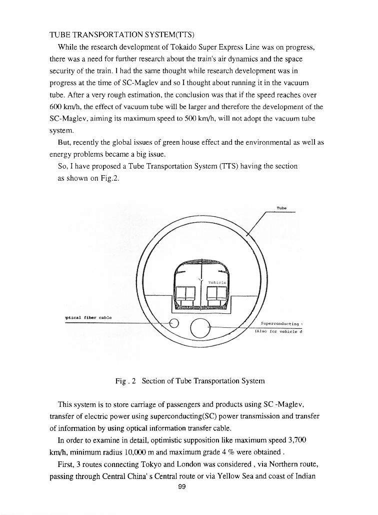
TUBE TRANSPORTATION SYSTEM(qq'S)
While the research developmentof Tokaido Super Express Line was on progress,
there was a need for further research about the train's air dynamics and the space
security of the train. I had the same thought while research development was in
progress at the time of SC-Maglev and so I thoughtabout running it in the vacuum
tube. After a very rough estimation, the conclusion was that if the speed reaches over
600 krn/h, the effect of vacuum tube will be larger and therefore the development of the
SC-Maglev, aiming its maximumspeed to 500 krn/h, will not adopt the vacuum tube
system.
But, recently the global issues of green house effect and the environmental as well as
energy problems became a big issue.
So, I have proposed a Tube Transportation System (TTS) having the section
as shown on Fig.2.
Tube
t/y t_tlcal fiber cable
Superconducting
(Alsofor vehicle d
Fig. 2 Section of Tube TransportationSystem
This system is to store carriage of passengers and products using SC -Maglev,
transfer of electric power using superconducting(SC)power transmission and transfer
of information by using optical information transfercable.
In order to examine in detail, optimisticsupposition like maximum speed 3,700
km/h, minimum radius 10,000m and maximumgrade 4 % were obtained.
First, 3 routes connecting Tokyo and London was considered, via Northern route,
passing through Central China' s Central route or via Yellow Sea and coast of Indian99

Ocean route of South route. The route Tokyo and London is a route connecting East
and West, so the route of South and North was also considered. To connect with the
above studies, hypothesis of London and Buenos Aires route was considered.
Then, in order to plan the development of the countries deeply involved to Japan
Sea, Pacific Rim Japan Sea Concept was proposed and investigated. Then, adding the
views of those people of China and Taiwan, who have the strong interest on this Japan
Sea Rim Concept, a hypothesis route shown in Fig.3 has been investigated. We call it
"East Asia Corridor Route" tentatively.The total distance of this new route will be
10,000km, the distance of mountain tunnel occupies 24.8 %, under water tunnel will
be 17.0 %. The objective of time around this route will be3 hours.The commercialize
opening of tunnel link
between Britain and France
channel this year will be the
starting point of this
concept.In order to materialize
this concept, the
cooperation of
professionals of
superconductive and o
macroengineering as well ,,
as experts from many fieldsare essential but above all
major necessity will be toraise the awareness of this _
concept to many people of :.the world. _
Fig.3 East Asia Corridor Route
100
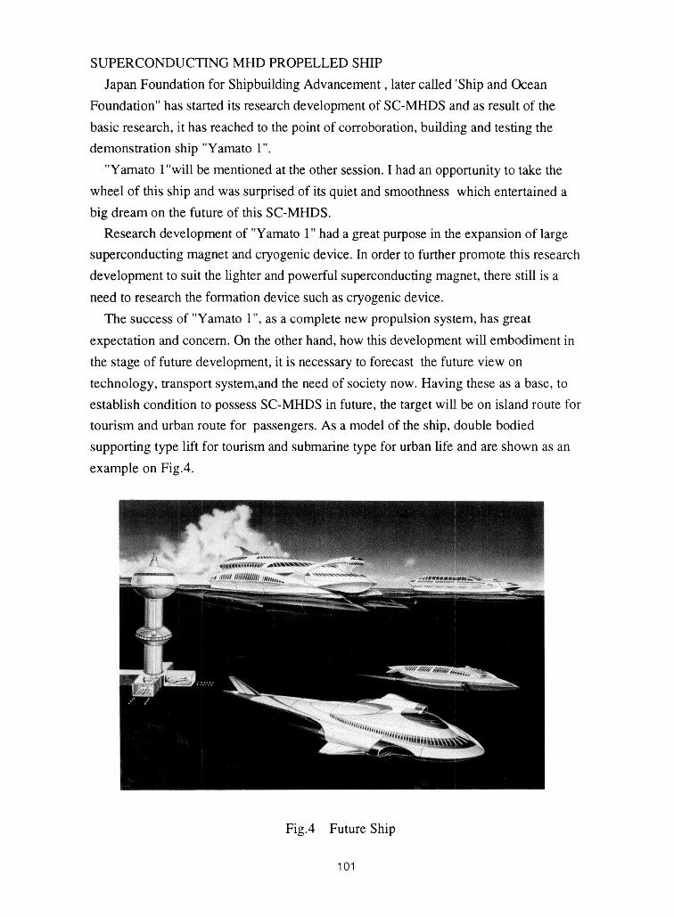
SUPERCONDUCTING MHD PROPELLED SHIP
Japan Foundation for ShipbuildingAdvancement, later called 'Ship and Ocean
Foundation" has started its research development of SC-MHDS and as result of the
basic research, it has reached to the point of corroboration,building and testing the
demonstration ship "Yamato 1".
"Yamato l"will be mentionedat the other session. I had an opportunity to take the
wheel of this ship and was surprised of its quiet and smoothness which entertained a
big dream on the future of this SC-MHDS.
Research development of "Yamato 1"had a great purpose in the expansion of large
superconducting magnet and cryogenic device. In order to furtherpromote this research
development to suit the lighter and powerful superconductingmagnet, there still is a
need to research the formation device such as cryogenic device.
The success of "Yamato 1", as a complete new propulsion system, has great
expectation and concern. On the other hand, howthis developmentwill embodiment in
the stage of future development, it is necessary to forecast the future view on
technology, transport system,and the need of society now. Having these as a base, toestablish condition to possess SC-MHDS in future, the target will be on island route for
tourism and urban route for passengers. As a model of the ship, double bodied
supporting type lift for tourism and submarine type for urban life and are shown as an
example on Fig.4.
Fig.4 Future Ship
101

EQUOS LIM CAR(ELC)
Railroad, in a broad sense guided ground transportation, is a transportation system
that runs with something by a ground guided system and has an advantage to run safely
on a high speed with connected carriagebut theguided line(rail)islimited and cannot
move freely. On the other hand, automobileshave an advantage to run freely but has to
head the vehicle to the direction by holding thesteering wheel, which has a limit to the
speed in human driving. Also, it is difficult to drive connectingmany cars like a
carriage. So I have investigateda vehiclehaving the advantageof both railroad andautomobile.
Intelligent of many countries are making a research and soon automobileswill beelectrified and automated.This direction is without fail definite and it would be an
opportunity to make research developmentof "new vehicle"which is neither an"automobile" nor a "railroad".
From the experience of the research developmentof small SC-motor with
SC-Maglev, I have thought that the futureautomobilewill be an electric car and its
implant will be rotating SC-motor or linear motorand therefore, I thought of combiningthese two motors for this new vehicle.
When driving in the city it will run as an usual automobile,rotating the wheels with
rotating superconductive motor which will result to no vibration, noiseless and
pollution, free. But on the highway, when the rotation of wheel is speeded, vehicle will
levitate and run with high speed. At this moment the guide power works in between
the ground and the car and it willdirect withoutanyone touching the steering wheels. It
is not a dream to reach maximum speed of 500 km/h.
This concept is possible because of thecombination of Linear Induction Motor (LIM)
and Electro-DynamicLevitation (ED) using rotating magneticfield. But on the ground
an arrangement of a electric conductorplate like aluminumplate is required.
A vehicle with this new concept is called EQUOSLIM CAR and in order to confirm
the possibility of this concept, we havemade and experimented a model shown in Fig.5
with EQUOS RESEARCH CO. On this experiment, permanentmagnet was used to see
the wheel travelling, ED, rotating magneticfield transfer with LIM propulsion
We have confirmed the condition of wheel travelling,levitation,levitated travelling,
landing, wheel travelling with the experiment device of about 26 m.long guideway with
a model car of 50 cm in length and 4 kg in weight.
102
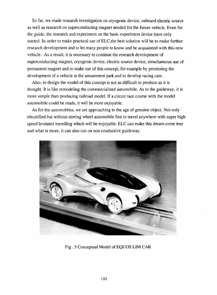
So far, we made research investigationon cryogenic device, onboard electric source
as well as research on superconductingmagnet needed for the future vehicle. Even for
the guide, the research and experimenton the basicexperimentdevice have only
started. In order to make practical use of ELC,the best solutionwill be to make further
research development and to let manypeople to know and be acquainted with this new
vehicle. As a result, it is necessary to continue the research development of
superconducting magnet, cryogenic device, electric source device, simultaneous use of
permanent magnet and to make use of this concept, for example by promoting the
development of a vehicle at the amusementpark and to develop racing cars.
Also, to design the model of this concept is not as difficult to produce as it is
thought. It is like remodeling the commercializedautomobile. As to the guideway, it is
more simple than producing railroad model. If a circuit race course with the model
automobile could be made, it will be more enjoyable.
As for the automobiles, we are approaching to the age of genuine object. Not only
electrified but without stirring wheel automobilefree to travel anywhere with super high
speed levitated travellingwhich will be enjoyable.ELC can make this dream come true
and what is more, it can also run on non conductive guideway.
Fig. 5 ConceptualModel of EQUOS LIM CAR
103
SUPERCONDUCTING CORRIDOR
So far I have mentioned the major transportationsystem applying superconductive.
For the development of large machineryas well as transportationsystem, the
sustenance test of actual structure is needed. Since the same thingcould be said for the
applied equipment of superconductive, the large scale test installation and support of
big financial capital are needed.
The cities in the past havecollected all kinds of functionsand many people gathered
to make use of its convenience which formed a city.There are cities developed as a
center for politics, administration, economics,commercial, industries, transportation
and tourism. Furthermore in order to develop the region, countries around the world
are considering to form a distinguishedcity furnished with special faculty. For
example, Hong Kong has developed as the free port for economy and the second and
the third Hong Kong are considered.
High technologies and new materialsas wellas superconductivewill provide affect
on future technology, industry or even in a broad sense economy. The research
development of high technologiesand new materialsmust be openedto the public all
over the world for the need to promote further research development.
Gathered the thoughts as mentioned above, I have proposed a thought of one city
and named and announced it as a "SuperconductingCity".
Later, part of content was published in a magazineand I havereceived a commission
on research investigation as to the application of superconductingcity from Iwaki City
in Fukushima Prefecture and as an interim report, I drew a superconducting city
concept based on Iwaki City. With this concept drawing, adding the result of
investigation research related to the undergrounddevelopmentand superconducting
magnetically propulsion ship from Power Reactor And NuclearFuel Development
Corporation, Ship and Ocean Foundation, the revised concept drawing is shown on
Fig. 6.
Below SMES is SC-Maglev and down left is the picture of superconducting linear
elevator. The building under the water is the terminalfor submarinetype SC-MHDS
and the link to the ground for passengers and cargoes will be SC-linear elevator. The
sky scraper building in the center has a height over 1,000m,and the former elevator will
have the problem of rope weight and have to change on the way. If SC-linear elevator
is used, there will be no need to change lift on the way because there will be no rope
used and also, it can pass over like a railroad and can reduce the surface area occupied.
In Japan, other than SC-linearelevator research development of normal conducting
linear elevator is in process.
104

The small picture at the right top of the drawing is the amusement park applying
superconductive and the building at the right is the hospital equipped with
superconductive applying equipment and the building on the left to the amusement park
is the information transmission center equipped with superconductive applied
equipments.
It is my dream to build a city where research developmentis free and I would like to
open this city to the world as a liberalcity of technologieswhere any people are free to
enter for the happiness of the humankind around the World.
Fig.6 Superconducting Corridor
CONCLUSION
The application of superconductiveis ranging in the wide field. Especially the
transportationfield is expected to make a big change. If the high temperature
superconductive is to materialize, the changewill make further development. It will be
my most concerned and appreciation,if the applicationof superconductiveleads to the
solution of the global issues of environmentand energy.
105
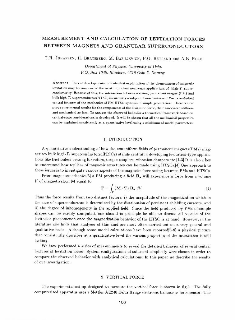
MEASUREMENT AND CALCULATION OF LEVITATION FORCES
BETWEEN MAGNETS AND GRANULAR SUPERCONDUCTORS
T.H. JOHANSEN, H. BRATSBERG, M. BAZILJEVICH, P.O. HETLANDand A.B. RIISE
Department of Physics, University of Oslo.
P.O. Box 1048, Blindern, 0316 Oslo 3, Norway.
Abstract - Recent developments indicate that exploitation of the phenomenon of magnetic
levitation may become one of the most important near-term applications of high-To super-
conductivity. Because of this, the interactiou between a strong permanent magnet(PM) andbulk high-Tc superconductor(HTSC) is currently a subject of much interest. We have studied
central features of the mechanics of PM-HTSC systems of simple geometries. Here we re-
port experimental results for the components of the levitation force, their associated stiffnessand mechanical ac-loss. To analyse the observed behavior a theoretical framework based on
critical-state considerations is developed. It will be shown that all the mechanical properties
can be explained consistently at a quantitative level using a minimum of model parameters.
1. INTRODUCTION
A quantitative understanding of how the nonuniform fields of permanent magnets(PMs) mag-
netizes bulk high-To superconductors(HTSCs) stands central in developing levitation-type applica-
tions like frictionless bearing for rotors, torque couplers, vibration dampers etc.[I-3] It is also a key
to understand how replicas of magnetic structures can be made using WI_SCs.[4] One approach to
these issues is to investigate various aspects of the magnetic force acting between PMs and HTSCs.
From magnetomechanics[5] a PM producing a field B_ will experience a force from a volumeV of magnetization M equal to
= Iv(M-V) B_ dV . (1)F
Thus the force results from two distinct factors; i) the magnitude of the magnetization which in
the case of superconductors is determined by the distribution of persistent shielding currents, and
ii) the degree of inhomogeneity in the applied field. Since the field produced by PMs of simple
shapes can be readily computed, one should in principle be able to discuss all aspects of the
levitation phenomenon once the magnetization behavior of the HTSC is at hand. However, in the
literature one finds that analyses of this kind are most often carried out on a very general and
qualitative basis. Although some model calculations have been reported[6-8] a physical picture
that consistently describes at a quantitative level the various properties of the interaction is stilllacking.
We have performed a series of measurements to reveal the detailed behavior of several central
features of levitation forces. System configurations of sufficient simplicity were chosen in order to
compare the observed behavior with analytical calculations. In this paper we describe the resultsof our investigation.
2. VERTICAL FORCE
The experimental set-up designed to measure the vertical force is shown in rigA. The fully
computerized apparatus uses a Mettler AE240 Delta Range electronic balance as force sensor. The
106
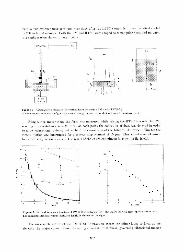
force versus distance measurements were done after tile HTSC sample had been zero-field cooled
to 77K in liquid nitrogen. Both the PM and HTSC were shaped as rectangular bars, and mounted
in a configuration shown in detail below.
PM
PM
taT il;::;::i::i::i::iii::i::i::i::i::i::!:;!::i::iiiiiiii::i::iil;iiiii!!!!::
;iiil;iiiiiiiiiiiiiiiiiiiiii;iiii_:_i::i::i
Figure 1: Apparatus to measure the vertical force between a PM and I'[TSC(left).
Magnet-superconductor configuration viewed along the y-axis(middle) and seen from above(right).
Using a step motor stage the force was measured while raising the HTSC towards the PM,
starting from a distance h = 20 ram. At each point the collection of data was delayed in orderto allow relaxations to decay below the 0.ling resolution of the balance. At every millimeter the
steady motion was interrupted for a reverse displacement of 15 /_m. This added a set of minor
loops in the F_ versus h curve. The result of the entire experiment is shown in fig.2(left).
' I ' ' I ' ] ' ' I ' ! ' I ' I '12 --o
to --. 100
10 -$_ '_
o_ E •
r;_" 32 10 • •oo
u__ 6 _, o ° oI •I •3_ 2_ O0 01
4 h 5 (ram) -- 1 •
2 -- •
4 8 12 16 20 4 8 12 16 20h (ram) h (ram)
Figure 2: Vertical force as a function of PM-HTSC dJstance.(left) The insert shows a close-up of a minor loop.
The magnetic stiffness versus levitation height is shown on the right.
The irreversible nature of the PM-HTSC interaction causes the minor loops to form an an-
gle with the major curve. Thus, the spring constant, or stiffness, governing vibrational motion
107
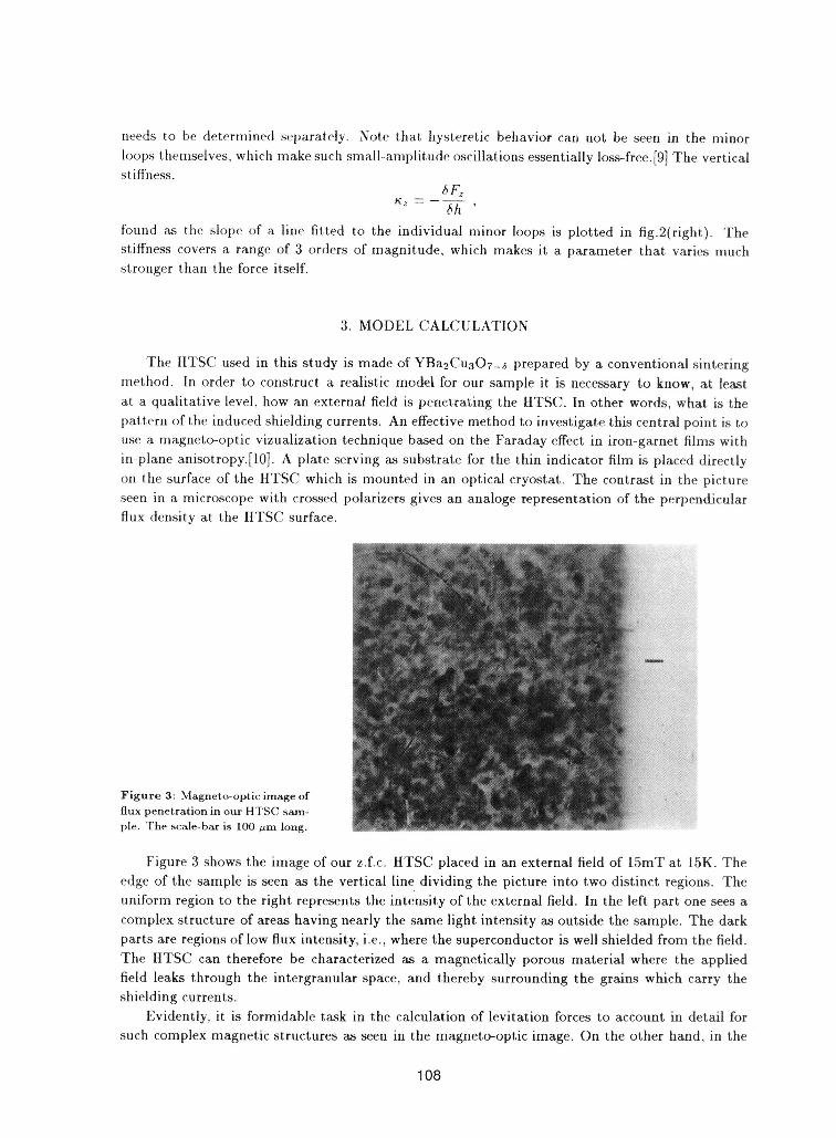
needs to be deternfined separately. Note that hysteretic behavior can not be seen in the nfinor
loops themselves, which make such small-amplitude oscillations essentially loss-free.J9] The verticalst iffness,
6F,6h
found as thc slope of a line fitted to the individual minor loops is plotted in fig.2(right). Thestiffness covers a range of 3 orders of magnitude, which makes it a parameter that varies much
stronger than the force itself.
3. MODEL CALCULATION
The HTSC used in this study is made of YBa2Cu3OT__ prepared by a conventional sintering
method. In order to construct a realistic mode| for our sample it is necessary to know, at least
at a qualitative level, how an external field is penetrating the HTSC. In other words, what is the
pattern of the induced shielding currents. An effective method to investigate this central point is to
use a magneto-optic vizualization technique based on the Faraday effect in iron-garnet films with
in-plane anisotropy.[10]. A plate serving as substrate for the thin indicator film is placed directly
on the surface of the HTSC which is mounted in an optical cryostat. The contrast in the picture
seen in a microscope with crossed polarizers gives an analoge representation of the perpendicularflux density at the HTSC surface.
Figure 3: Magneto-optic image of
flux penetration in our HTSC saxn-
pie. The scale-bar is 100/_m long.
Figure 3 shows the image of our z.f.c. HTSC placed in an external field of i5mT at 15K. The
edge of the sample is seen as the vertical line dividing the picture into two distinct regions. Theuniform region to the right represents the intensity of the external field. In the left part one sees a
complex structure of areas having nearly the same light intensity as outside the sample. The dark
parts are regions of low flux intensity, i.e., where the superconductor is well shielded from the field.
The HTSC can therefore be characterized as a magnetically porous material where the applied
field leaks through the intergranular space, and thereby surrounding the grains which carry the
shielding currents.
Evidently, it is formidable task in the calculation of levitation forces to account in detail for
such complex magnetic structures as seen in the magneto-optic image. On the other hand, in the
108
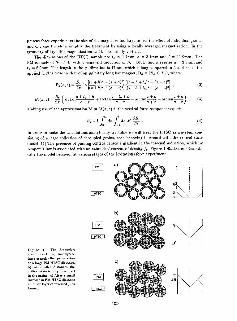
present force experiments the size of the magnet is too large to feel the effect of individual grains,and one can therefore simplify the treatment by using a locally averaged magnetization. In the
geometry of fig.1 this magnetization will be essentially vertical.The dimensions of the HTSC sample are tb = 1.7ram, b = 3.4mm and l = ll.gmm. The
PM is made of Nd-Fe-B with a remanent induction of B,=I.05T, and measures a = 2.8ram andta = 6.0mm. The length in the y-direction is 17ram, which is long compared to l, and hence the
applied field is close to that of an infinitely long bar magnet, Ba = (B_, O,Bz), where
S=(x,z)= B, [(z+h) 2+(x-a)ln[(z+h) 2+(x-a) 2][(z+h+t_) _+(x_a) 2] ' (2)
Br ( z+t_+h+arctan z+ta+h arctanZ+h-arctanZ+h_ . (3)Bz(x,z)=_-_ arctan a+x a-x a+x a-x]
Making use of the approximation M ---M(x, z) z, the vertical force component equals
fo'bdz/_bFz = l dz M -- (4)b Oz
In order to make the calculations analytically tractable we will treat the HTSC as a system con-
sisting of a large collection of decoupled grains, each behaving in accord with the critical state
model.[ll] The presence of pinning centres causes a gradient in the internal induction, which byAmpere's law is assx)ciated with an azimuthal current of density jc. Figure 4 illustrates schemati-
cally the model behavior at various stages of the levitations force experiment.
a) iIIIII
III
b)
Figure 4: The decoupledgrain model, a) Incompleteintra-granulax flux penetration
at a large PM-HTSC distance. C)
b) At smaller distances thecritical state is fully developed [
Iin the grains, c) After a small [-PM-[increasein PM-HTSCdistancean outer layerof reversedjc isformed.
109
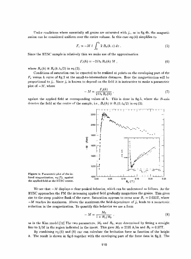
Under conditions where essentially all grains are saturated with jc, as in fig.4b, the magneti-
zation can be considered uniform over the entire volume. In this case eq.(4) simplifies to
F: = -M l 2 B_.(b, z) dz . (5)
Since the HTSC sample is relatively thin we make use of the approximation
Fz(h) = --2ltbB,:(h)M, (6)
where B_:(h) = B_:(b, tb/2) in eq.(2).
Conditions of saturation can be expected to be realized at points on the enveloping part of the
Fz versus h curve of fig.2 at the small-to-intermediate distances. Here the magnetization will be
proportional to j_. Since jc is known to depend on the field it is instructive to make a parametricplot of -M, where
- M = Fz(h)2ltb B_(h) ' (7)
against the applied field at corresponding values of h. This is done in fig.5, where tile B-axis
denotes the field at the centre of the sample, i.e., Bz(h) -- B:IO, tb/2) in eq.(3).
_o tla':,Oo• _.
i "%""%': •2000 _ " ".-.
• *°••°•••. •. • •• . •• • °
• .1800 :
E i °_' ' ' ' '
:_ 16oo - • -
.
1400 -: _ oooos; --! i
1200 -: _ --
, I , I , I ' I ,ooo 0o5 olo o s o_o o2sBz (T)
Figure 5: Parametric plot of the in-fered magnetization, eq.(7), against 1000 , , , I I I , , , I I I I I I I I I I I I f t I0.00 0.05 0.10 0.15 0.20 0.25
the applied field at the HTSC centre. Bz (T )
We see that -M displays a clear peaked behavior, which can be understood as follows. As the
HTSC approaches the PM the increasingapplied field gradually magnetizes the grains. This givesrise to the steep positive flank of the curve. Saturation appears to occur near B_ = 0.025T, where
-M reaches its maximum. Above the maximum the field-dependence of j_ leads to a monotonic
reduction in the magnetization. To quantify this behavior we use a form
Iv/0- M - (8)1 + B_/Bo
as in the Kim model.[12] The two parameters, M0 and B0, were determined by fitting a straight
line to 1/M in the region indicated in the insert. This gave M0 = 2195 A/m and B0 = 0.97T.
By combining eq.(6) and (8) one can calculate the levitation force as function of the height
h. The result is shown in fig.6 together with the enveloping part of the force data in fig.2. The
110
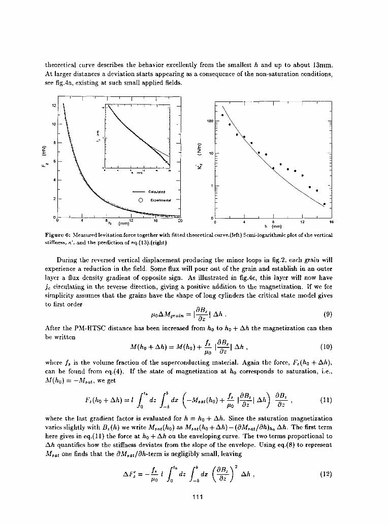
theoretical curve describes the behavior excellently from the smallest h and up to about 13ram.
At larger distances a deviation starts appearing as a consequence of the non-saturation conditions,see fig.4a, existing at such small applied fields.
lO12 _ I l t loo ' I _ I ' I '
_" Z 10 •
6
LL N -_ •L = I =
4
1 •
2
O0 4 8 h (mm)12 16 20 0 I ! I I i I I4 8 12 16
h (mm)
Figure 6: Measured levitation force together with fitted theoretical curve.(left) Semi-logarithmlc plot of the vertical
stiffness, n', and the prediction of eq.(13).(right)
During the reversed vertical displacement producing the minor loops in fig.2, each grain will
experience a reduction in the field. Some flux will pour out of the grain and establish in an outer
layer a flux density gradient of opposite sign. As illustrated in fig.4c, this layer will now have
jc circulating in the reverse direction, giving a positive addition to the magnetization. If we for
simplicity assumes that the grains have the shape of long cylinders the critical state model givesto first order
v0AMg,o,.= 10B'IOz Ah. (9)After the PM-HTSC distance has been increased from h0 to h0 + Ah the magnetization can thenbe writtcn
L OB, IM(ho+Ah)= M(ho).-_o _ Ah, (10)
where fs is the volume fraction of the superconducting material. Again the force, Fz(ho -t- Ah),
can be found from eq.(4). If the state of magnetization at h0 corresponds to saturation, i.e.,
M(h0) = -M,_t, we get
i"/2( ", )F_(ho + Ah) = l dz dz -M.,.(ho) + ,OB. (11)OBz
b p--_ --ff_-zl Ah 0-.-_--_ ,
where the last gradient factor is evaluated for h = h0 + Ah. Since the saturation magnetization
varies slightly with Bz(h) we write M, at(h0) as M, at(h0 +Ah)- (OM, ot[Oh)ho Ah. The first term
here gives in eq.(11) the force at h0 + Ah on the enveloping curve. The two terms proportional toAh quantifies how the stiffness deviates from the slope of the envelope. Using eq.(8) to represent
M,_t one finds that the OM,_t/Oh-term is negligibly small, leaving
AF" = -f'Po i d: b dx \"-_'-z ) Ah , (12)
111
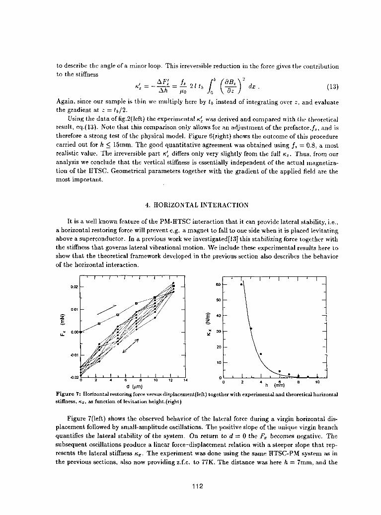
to describe the angle of a minor loop. This irreversible reduction in the force gives the contributionto the stiffness
., AF_ _ B 21tb fo dz. (13)_z - Ah P0
Again, since our sample is thin we multiply here by tb instead of integrating over z, and evaluatethe gradient at z = tb/2.
"' was derived and compared _vith the theoreticalUsing the data of fig.2Ileft) the experimental _z
result, eq.(13). Note that this comparison only allows for aa adjustment of the prefactor,fs, and is
therefore a strong test of the physical model. Figure 6(right) shows tile outcome of this procedure
carried out for h < 15mm. The good quantitative agreement was obtained using f, = 0.8, a most
realistic value. The irreversible part n'z differs only very slightly from the full tcz. Thus, from our
analysis we conclude that the vertical stiffness is essentially independent of the actual magnetiza-
tion of the HTSC. Geometrical parameters together with the gradient of the applied field are themost important.
4. HORIZONTAL INTERACTION
It is a well known feature of the PM-HTSC interaction that it can provide lateral stability, i.e.,
a horizontal restoring force will prevent e.g. a magnet to fall to one side when it is placed levitating
above a superconductor. In a previous work we investigated[13] this stabilizing force together withthe stiffness that governs lateral vibrational motion. We include these experimental results here to)
show that the theoretical framework developed in the previous section also describes the behaviorof the horizontal interaction.
' /. ' _ ' I ' I0.02 60 --
50
001
x 30u._ o._o_
20
,,0.01
10
-0.o2 0 _ I - d,0 2 4 6 8 10 12 14 0 2 4 h (m6m) e 10cl (_m)
Figure 7: !torizontal restoring force versus displacement(left) together with experimental and theoreticalhorizontalstiffness, nz, as function of levitation height.(right)
Figure 7(left) shows the observed behavior of the lateral force during a virgin horizontal dis-
placement followed by small-amplitude oscillations. The positive slope of the unique virgin branch
quantifies the lateral stability of the system. On return to d = 0 the F_ becomes negative. The
subsequent oscillations produce a linear force-displacement relation with a steeper slope that rep-
resents the lateral stiffness t¢_. The experiment was done using the same HTSC-PM system as in
the previous sections, also now providing z.f.c, to 77K. The distance was here h = 7ram, and the
112
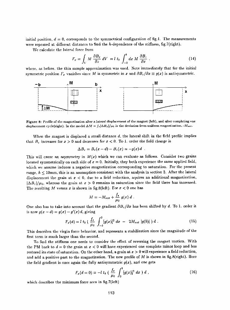
initial position, d = 0, corresponds to the symmetrical configuration of fig.l. The measurementswere repeated at different distances to find the h-dependence of the stiffness, fig.7(right).
We calculate the lateral force from
f_ _B /; OBz (14)F_ = M ----L dV = l tb dx M _ ." b
where, as before, the thin sample approximation was used. Note immediately that for the initialsymmetric position F_ vanishes since M is symmetric in x and OB_/Ox = g(z) is antisymmetric.
-b M b M> . )
t , II I
i
! ' I
Figure 8: Profile of the magnetization after a lateral displacement of the magnet (left), and after completing onedisplacement cycle(right). In the model AM = fs lAB= I/#0 is the deviation from uniform magnetization, -]lIsat.
When the magnet is displaced a small distance d, the lateral shift in the field profile impliesthat Bz increases for x > 0 and decreases for x < 0. To 1. order the field change is
AB_ = Bz(z- d)- B_(z) = -g(z)d .
This will cause an asymmetry in M(z) which we can evaluate as follows. Consider two grains
located symmetrically on each side of z = 0. Initially, they both experience the same applied field,which we assume induces a negative magnetization corresponding to saturation. For the present
range, h < 10mm, this is an assumption consistent with the analysis in section 3. After the lateraldisplacement the grain at x < 0, due to a field reduction, aquires an additional magnetization,Iz-XB_l/_0,whereas the grain at z > 0 remains in saturation since the field there has increased.The resulting M versus z is shown in fig.8(left). For z < 0 one has
_l : -Msat + fs g(z) d .
One also has to take into account that the gradient OB,/ax has been shifted by d. To 1. order it
is now g(z - d) = g(z) - g'(z) d, giving
[g/=)]2d= - 2M,o,Ig(b)l)d. (15)V (d)=t tb bThis describes the virgin force behavior, and represents a stabilization since the magnitude of the
first term is much larger than the second.To find the stiffness one needs to consider the effect of reversing the magnet motion. With
the PM back to d = 0 the grain at z < 0 will have experienced one complete minor loop and hasrestored its state of saturation. On the other hand, a grain at z > 0 will experience a field reduction,
and add a positive part to the magnetization. The new profile of M is shown in fig.8(right). Herethe field gradient is once again the fully antisymmetric g(z), and one gets
I°f0'F,(d = O) = -I tb ( _o [g(z)] _ dx ) d, (16)
which describes the minimum force seen in fig.7(left)
113
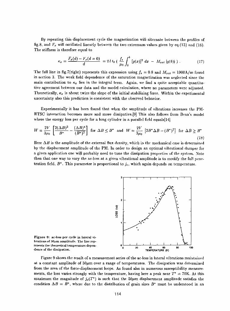
By repeating this displacement cycle the magnetization will alternate between the profiles of
fig.8, and F, will oscillated linearly between the two cxtremum values given by eq.(15) and (16).The stiffness is therefore equal to
F_(d) - F_.(d = O) f, [bKx = -_ = 21tb ( _0 .v [g(x)] = dx - M_t Ig(b)l ) • (17)
The full line in fig.7(right) represents this expression using f_ = 0.8 and M,_t = 1900A/m foundin section 3. The weak field dependence of the saturation magnetization was neglected since the
main contribution to K_, lies in the integral term. Again, we find a quite acceptable quantita-
tive agreement between our data and the model calculation, where no parameters were adjusted.
Theoretically, K:: is about twice the slope of the initial stabilizing force. Within the experimentaluncertainty also this prediction is consistent with the observed behavior.
Experimentally it has been found that when the amplitude of vibrations increases the PM-
HTSC interaction becomes more and more dissipative.J9] This also follows from Bean's model
where the energy loss per cycle for a long cylinder in a parallel field equals[14]
W= 2__VV[2(AB, 3 (AB)'] for AB<B* and iV= 2___VV[2B. AB_(B.,2 ] for AB> B"art0 L B* (B*)_J - 3_0 -
Here AB is the amplitude of the external flux density, which in the mechanical case is determined
by the displacement amplitude of the PM. In order to design an optimal vibrational damper fora given application one will probably need to tune the dissipation properties of the system. Note
then that one way to vary the ac-loss at a given vibrational amplitude is to modify the full pene-
tration field, B*. This parameter is proportional to jc, which again depends on temperature.
3 ' I _ I ' I ' I '
2v
9
1
Figure 9: ac-loss per cycle in lateral vi- \brations of 50/_m amplitude. The line rep-
resents the theoretical temperature depen- 0 I I i I J I t I
dence of the dissipation. 0 20 40 6o 8o looTEMPERATURE (Ix')
Figure 9 shows the result of a measurement series of the ac-loss in lateral vibrations maintained
at a constant amplitude of 50pm over a range of temperatures. The dissipation was determined
from the area of the force-displacement loops. As found also in numerous susceptibility measure-
ments, the loss varies strongly with the temperature, having here a peak near T* = 70K. At this
maximum the magnitude of jc(T*) is such that the 50pm displacement amplitude satisfies the
condition AB = B*, where due to the distribution of grain sizes B* must be understood in an
114
average sense. The expressions of eq.(18), modified by V ---. fsV to account for the magneticporosity of the HTSC, were fitted to our loss data. A temperature dependence of jc of the formjc(T) _x(1 - T/Te) p was a._unled. Best fit was obtained for p = 3/2, and the result is seen in the
graph as a full line. Again a very good quantitative agreement is obtained.A detailed description of the loss experiment together with a more comprehensive theoretical
analysis will be published soon.[15]
5. CONCLUDING REMARKS
Several key parameters characterizing the mechanics of magnetic levitation with ItTSCs havebeen investigated experimentally and theoretically. We have shown that (1)the repulsive verticalforce and its associated stiffness, (2) the lateral stabilizing force and the stiffness governing hori-zontal vibrations and (3) the temperature dependence of the mechanical ac-loss can be explainedat a quantitative level and with a minimum of adjustable parameters. For the first time, analyticalexpressions for all these quantities have been derived consistently for a model system. By doing so
it is brought out in detail how different parameters such as geometry and the magnetic responseof the superconductor affect the behaviors.
In this work we chose to study a sintered HTSC instead of a melt-processed bulk sample. The
reason is that melt-processed HTSCs tend to consist of grains many orders of magnitude largerthan in sintered samples. Although large grains give rise to large levitation forces, it will also pro-duce a local magnetization that varies over distances of the same scale as the size of the levitatingmagnet. To account quantitatively for the forces in such cases one probably needs to consider thedetailed structure of weak links, or the large-scale flow pattern of the shielding currents in eachindividual HTSC sample. This problem was avoided here by averaging over many small grains.
The authors wish to thank prof. Y. Galperin for stimulating discussions. The financial support
by The Research Council of Norway (Norges Forskningsr_d) is gratefully acknowledged.
References
1. BAR. Weinberser , L. Lynch and J.R. Hull, Supercond. Scl. Technol. 3, 381 (1990).
2. F.C. Moon, C.Golkowsld and D. Kupperman, Appl. Supercond. 1, 1175 (1993).
3. K.B. Ma, C.K. McMichael, M.A. Lamb and W.K. Chu, [EEE Trans. Appl. Supercond. 3, 388 (1993).
4. [.-G. Chen, J. Liu, R. Weinstein and K. Lau, J. Appl. Phys. 72, 1013 (1992).
5. see e.g., F.C. Moon, "Masneto-Solld Mechanics", New York, John Wiley & Sons, 1984.
6. F. Hellman, E.M. Gyorgy, D.W. Johnson Jr., H.M. O'Brian and R.C. Sherwood, J. Appl. Phys. 63 447,(1988).
7. L.C. Davis, J. Appl. Phys. 67 2631 (1990).
8. T. Torng and Q.Y. Chen, J. Appl. Phys. 73 1198 (1993).
9. T.H. Johansen, H. Bratsberg, Z.J. Yang, S.J. Guo and B. Loberg, J. Appl. Phys. 70, 7496 (1991).
10. A.A. Polyanskii, V.K. Vlasko-Vlasov, M.V. Indenbom and V.I. Nikitenko, Soy. Tech. Phys. Lett. 15, 872(1989).
11. C.P. Bean, Phys. Rev. Lett. 8, 250 (1962).
12. Y.B. Kim, C.F. Hempstead and A.R. Strnad, Phys. Rev. 129, 528 (1963).
13. T.H. Johansen, H. Mestl and H. Bratsberg, J. Appl. Phys. 75, (1994).
14. R. B. Goldfarh, M. Lelental, C. A. Thompson in "Magnetic Susceptibility of Superconductors and OtherSpin Systems" edited by R. A. Hein, T. L. Francavilla, D. H. Libenherg, New York, Plenum Press, 1991.
15. P.O. Hetland, H. Bratsberg and T.H. Jo_n(to be published).
115
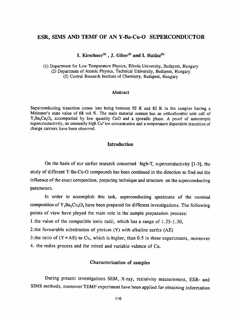
ESR, SIMS AND TEMF OF AN Y-Ba-Cu-O SUPERCONDUCTOR
I. Kirschner_) , J. Giber_:)and I. Hal_z _)
(1) DepartmentforLowTemperaturePhysics,E6tv6sUniversity,Budapest,Hungary(2) Departmentof AtomicPhysics,TechnicalUniversity,Budapest,Hungary
(3) CentralResearchInstituteof Chemistry,Budapest,Hungary
Abstract
Superconducting transition comes into being between 92 K and 82 K in the samples having aMeissner's state value of 68 vol. %. The main material content has an orthorhombic unit cell of
YIBa2Cu4Os accompanied by low quantity CuO and a sporadic phase. A proof of anisotropicsuperconductivity, an unusually high Cu" ion concentration and a temperature dependent transition ofcharge carriers have been observed.
Introduction
On the basis of our earlier research concerned high-To superconductivity [1-3], the
study of different Y-Ba-Cu-O compounds has been continued in the direction to find out the
influence of the exact composition, preparing technique and structure on the superconducting
parameters.
In order to accomplish this task, superconducting specimens of the nominal
composition of Y_Ba2Cu4Oshave been prepared for different investigations. The following
points of view have played the main role in the sample preparation process:
1.the value of the compatible ionic radii, which has a range of 1.25-1.30,
2.the favourable substitution of yttrium (Y) with alkaline earths (AE)
3.the ratio of (Y+AE) to Cu, which is higher, than 0.5 in these experiments, moreover
4. the redox process and the mixed and variable valence of Cu.
Characterization of samples
During present investigations SEM, X-ray, resistivity measurement, ESR- and
SIMS methods, moreover TEMF experiment have been applied for obtaining information
116
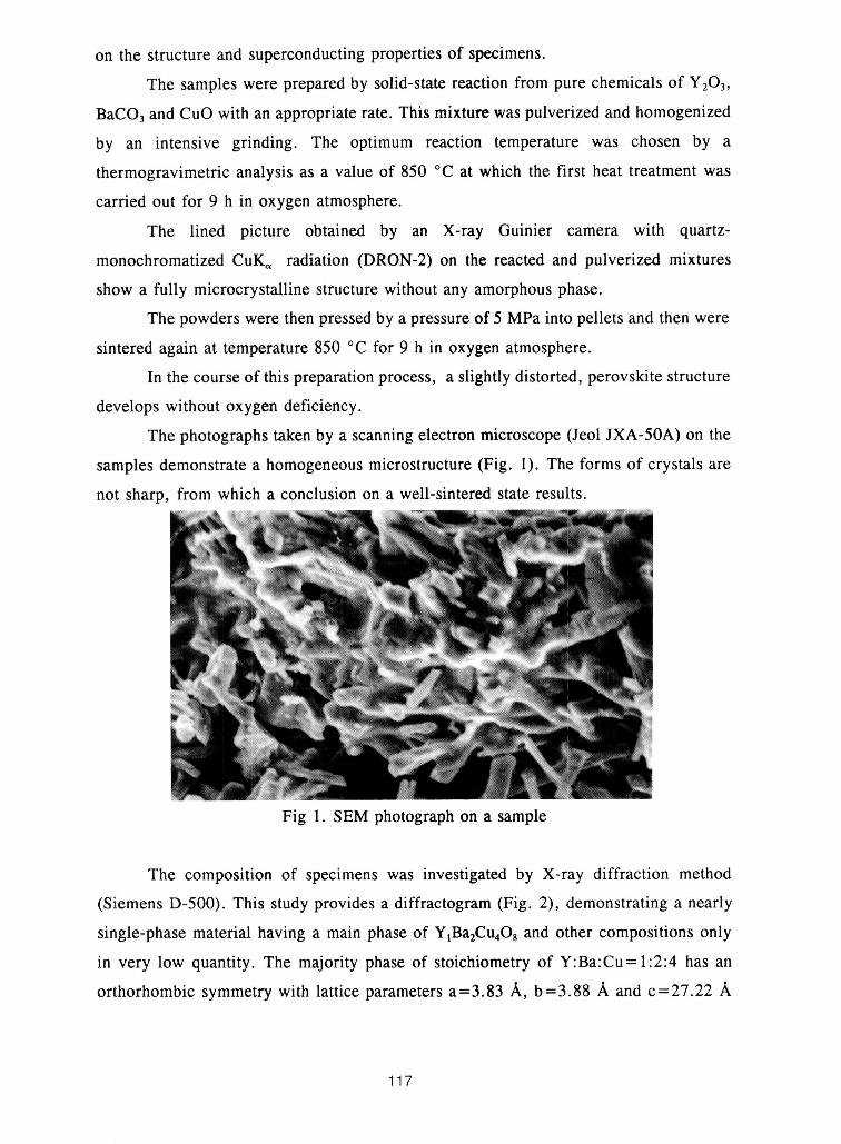
on the structure and superconducting properties of specimens.
The samples were prepared by solid-state reaction from pure chemicals of Y203,
BaCO3and CuO with an appropriate rate. This mixture was pulverized and homogenized
by an intensive grinding. The optimum reaction temperature was chosen by a
thermogravimetric analysis as a value of 850 °C at which the first heat treatment was
carried out for 9 h in oxygen atmosphere.
The lined picture obtained by an X-ray Guinier camera with quartz-
monochromatized CuK_ radiation (DRON-2) on the reacted and pulverized mixtures
show a fully microcrystalline structure without any amorphous phase.
The powders were then pressed by a pressure of 5 MPa into pellets and then were
sintered again at temperature 850 °C for 9 h in oxygen atmosphere.
In the course of this preparation process, a slightly distorted, perovskite structure
develops without oxygen deficiency.
The photographs taken by a scanning electron microscope (Jeol JXA-50A) on the
samples demonstrate a homogeneous microstructure (Fig. 1). The forms of crystals are
not sharp, from which a conclusion on a well-sintered state results.
Fig 1. SEM photograph on a sample
The composition of specimens was investigated by X-ray diffraction method
(Siemens D-500). This study provides a diffractogram (Fig. 2), demonstrating a nearly
single-phase material having a main phase of Y_Ba2Cu408and other compositions only
in very low quantity. The majority phase of stoichiometry of Y:Ba:Cu=I:2:4 has an
orthorhombic symmetry with lattice parameters a=3.83 /k, b=3.88 /k and c=27.22 /k
117
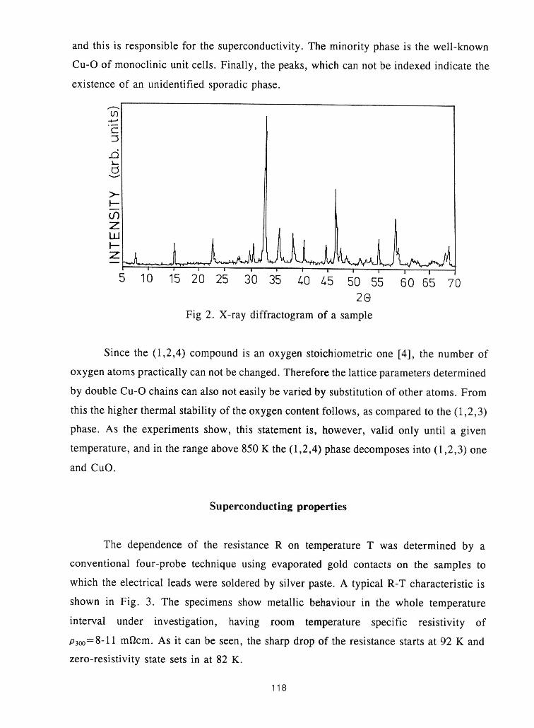
and this is responsible for the superconductivity. The minority phase is the well-known
Cu-O of monoclinic unit cells. Finally, the peaks, which can not be indexed indicate the
existence of an unidentified sporadic phase.
>.I--
zu_lI---z
5 10 15 20 25 3'0 35 40 /-.5 50 55 60 65 702E)
Fig 2. X-ray diffractogram of a sample
Since the (1,2,4) compound is an oxygen stoichiometric one [4], the number of
oxygen atoms practically can not be changed. Therefore the lattice parameters determined
by double Cu-O chains can also not easily be varied by substitution of other atoms. From
this the higher thermal stability of the oxygen content follows, as compared to the (1,2,3)
phase. As the experiments show, this statement is, however, valid only until a given
temperature, and in the range above 850 K the (1,2,4) phase decomposes into (1,2,3) one
and CuO.
Superconducting properties
The dependence of the resistance R on temperature T was determined by a
conventional four-probe technique using evaporated gold contacts on the samples to
which the electrical leads were soldered by silver paste. A typical R-T characteristic is
shown in Fig. 3. The specimens show metallic behaviour in the whole temperature
interval under investigation, having room temperature specific resistivity of
p3oo=8-11mftcm. As it can be seen, the sharp drop of the resistance starts at 92 K and
zero-resistivity state sets in at 82 K.
118
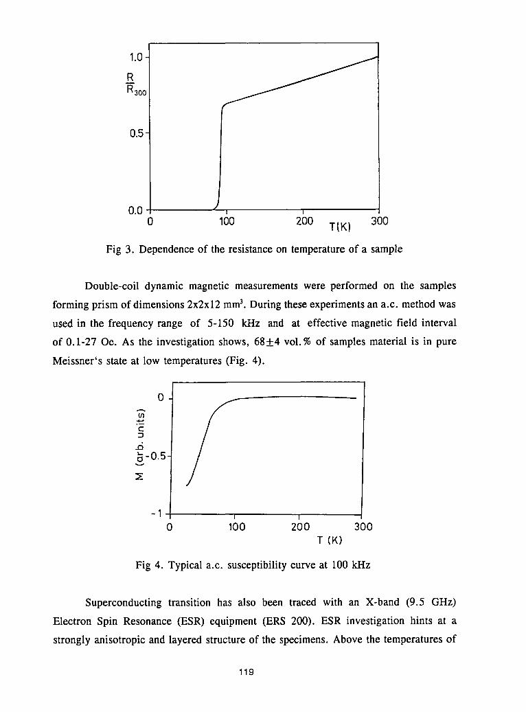
10R3oc
0.5
0.0 _ i i
0 100 200 T(K) 300
Fig 3. Dependence of the resistance on temperature of a sample
Double-coil dynamic magnetic measurements were performed on the samples
forming prism of dimensions 2x2x12 mm3. During these experiments an a.c. method was
used in the frequency range of 5-150 kHz and at effective magnetic field interval
of 0.1-27 Oe. As the investigation shows, 68+4 vol. % of samples material is in pure
Meissner's state at low temperatures (Fig. 4).
0A
°_
€..
.6-0.5,
_1 _i i I
0 100 200 300T (K)
Fig 4. Typical a.c. susceptibility curve at 100 kHz
Superconducting transition has also been traced with an X-band (9.5 GHz)
Electron Spin Resonance (ESR) equipment (ERS 200). ESR investigation hints at a
strongly anisotropic and layered structure of the specimens. Above the temperatures of
119
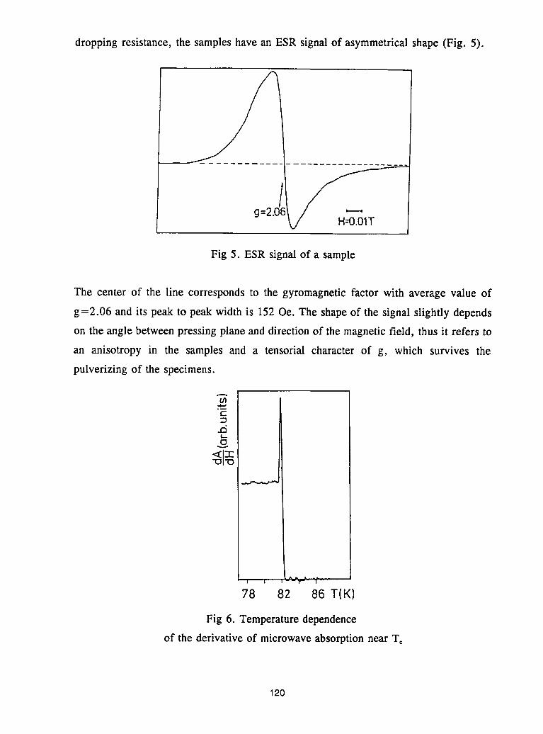
dropping resistance, the samples have an ESR signal of asymmetrical shape (Fig. 5).
H=O.O1T
Fig 5. ESR signal of a sample
The center of the line corresponds to the gyromagnetic factor with average value of
g=2.06 and its peak to peak width is 152 Oe. The shape of the signal slightly depends
on the angle between pressing plane and direction of the magnetic field, thus it refers to
an anisotropy in the samples and a tensorial character of g, which survives the
pulverizing of the specimens.
t/!._
t"
i._
_'-r-
78 82 86 T(K)
Fig 6. Temperature dependence
of the derivative of microwave absorption near Tc
120
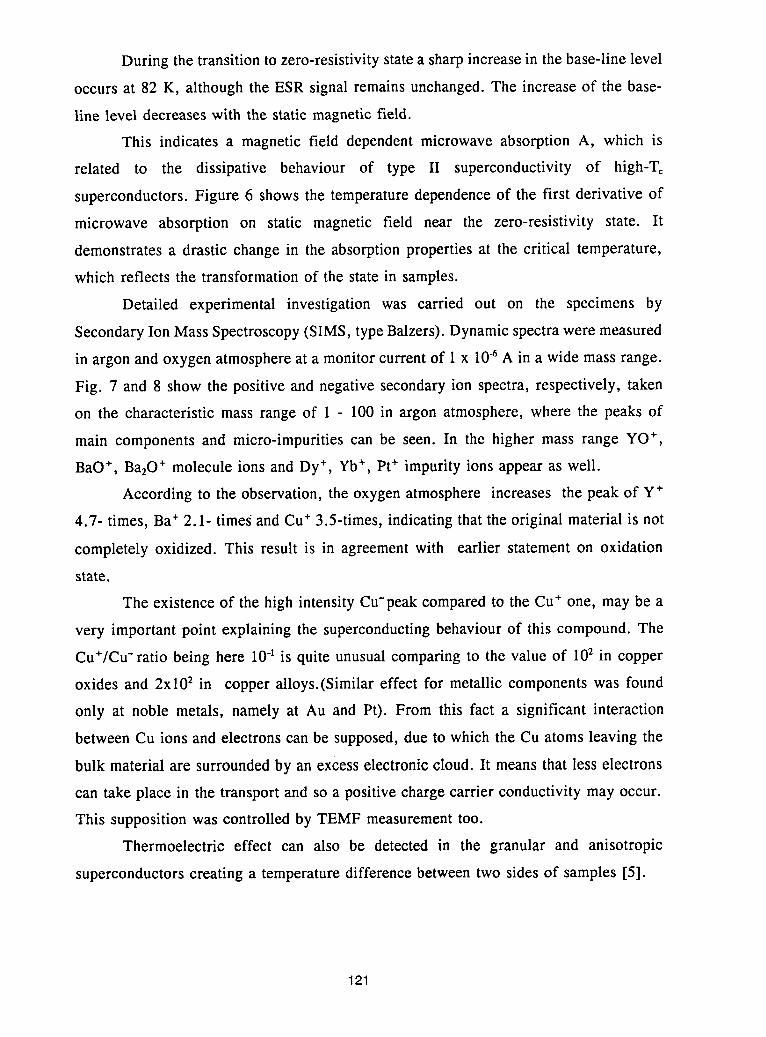
During the transition to zero-resistivity state a sharp increase in the base-line level
occurs at 82 K, although the ESR signal remains unchanged. The increase of the base-
line level decreases with the static magnetic field.
This indicates a magnetic field dependent microwave absorption A, which is
related to the dissipative behaviour of type II superconductivity of high-To
superconductors. Figure 6 shows the temperature dependence of the first derivative of
microwave absorption on static magnetic field near the zero-resistivity state. It
demonstrates a drastic change in the absorption properties at the critical temperature,
which reflects the transformation of the state in samples.
Detailed experimental investigation was carried out on the specimens by
Secondary Ion Mass Spectroscopy (SIMS, type Balzers). Dynamic spectra were measured
in argon and oxygen atmosphere at a monitor current of 1 x 10⁻⁶A in a wide mass range.
Fig. 7 and 8 show the positive and negative secondary ion spectra, respectively, taken
on the characteristic mass range of 1 - 100 in argon atmosphere, where the peaks of
main components and micro-impurities can be seen. In the higher mass range YO .,
BaO., Ba20 . molecule ions and Dy., Yb., Pt. impurity ions appear as well.
According to the observation, the oxygen atmosphere increases the peak of Y.
4.7- times, Ba. 2.1- times and Cu. 3.5-times, indicating that the original material is not
completely oxidized. This result is in agreement with earlier statement on oxidation
state.
The existence of the high intensity Cu-peak compared to the Cu. one, may be a
very important point explaining the superconducting behaviour of this compound. The
Cu+/Cu" ratio being here 10-I is quite unusual comparing to the value of 102in copper
oxides and 2x10² in copper alloys.(Similar effect for metallic components was found
only at noble metals, namely at Au and Pt). From this fact a significant interaction
between Cu ions and electrons can be supposed, due to which the Cu atoms leaving the
bulk material are surrounded by an excess electronic cloud. It means that less electrons
can take place in the transport and so a positive charge carrier conductivity may occur.
This supposition was controlled by TEMF measurement too.
Thermoelectric effect can also be detected in the granular and anisotropic
superconductors creating a temperature difference between two sides of samples [5].
121
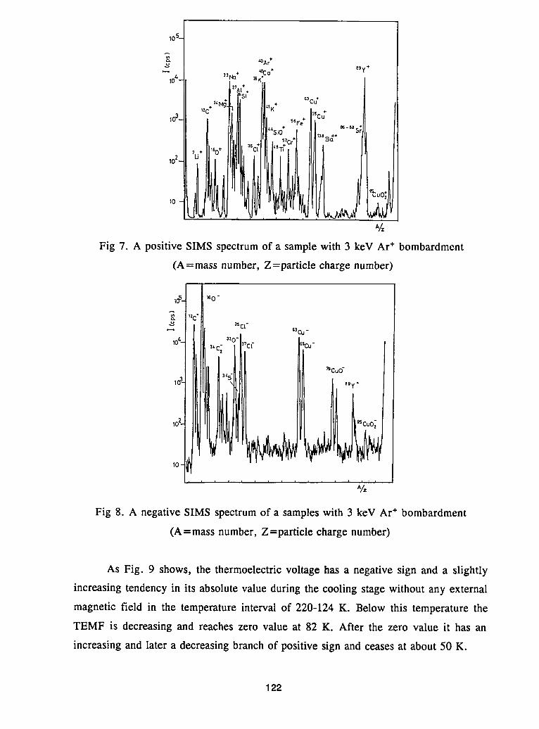
%0;lo
Fig 7. A positive SIMS spectrum of a sample with 3 keV Ar. bombardment
(A=mass number, Z=particle charge number)
%
Fig 8. A negative SIMS spectrumof a sampleswith 3 keV Ar+ bombardment
(A=mass number, Z=particle charge number)
As Fig. 9 shows, the thermoelectric voltage has a negative sign and a slightly
increasing tendency in its absolute value during the cooling stage without any external
magnetic field in the temperature interval of 220-124 K. Below this temperature the
TEMF is decreasing and reaches zero value at 82 K. After the zero value it has an
increasing and later a decreasing branch of positive sign and ceases at about 50 K.
122
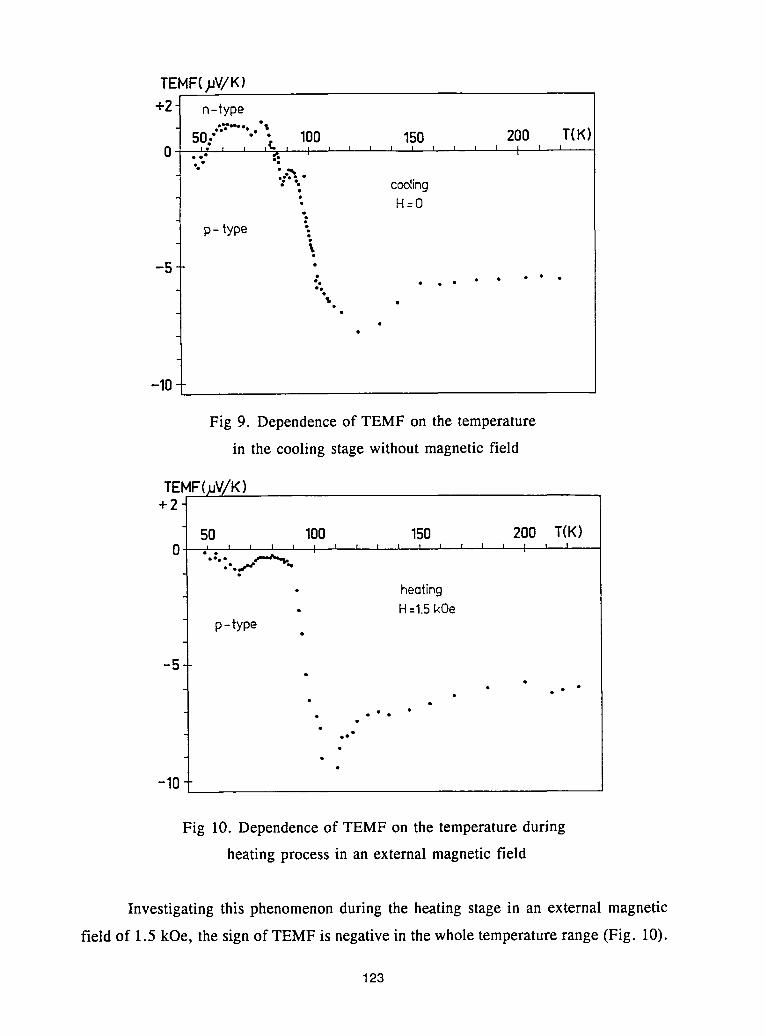
TENIF()JV/K)
+2 - n-type
• ° •50: . 100 150 200 T(K)
?""%" " cooling++• t4=0
p- type%
-5 °° °
%
-10
Fig 9. Dependence of TEMF on the temperature
in the cooling stage without magnetic field
TEMF(juV/K)+2
50 100 150 200 T(K)0 .' • T i I T I I f I I T T i , i I I I
• heating• H=1.5kOe
p-type
-5
oo
-KI
Fig 10. Dependence of TEMF on the temperature during
heating process in an external magnetic field
Investigating this phenomenon during the heating stage in an external magnetic
field of 1.5 kOe, the sign of TEMF is negative in the whole temperature range (Fig. 10).
123
Starting from 50 K, the curve of TEMF firstly has an increasing character in its absolute
value until 110 K. At this point a sharp break then a moderate decrease and a saturation
tendency in the investigated temperature interval (until 220 K) can be observed.
If a temperature gradient exists in the sample between two opposite surfaces, the
charge carriers diffuse from higher-temperature side to the lower-temperature one until
a stationary voltage difference established. In the case of p-type charge carriers the cold
surface will be more positive and in the presence of n-type ones, more negative. This
phenomenon represents a positive-negative transition of the charge carriers occurring at
the temperature of zero-resistivity state. In contrast with this observation there is no
change in dominant carriers during the heating stage in an applied external magnetic
field.
Comparing the magnitude of the effect in other materials, the obtained voltage
signals are generally higher, than those for metals and lower, than the thermal voltages
belonging to semiconductors. The obtained TEMF values were independent from the
materials (bronze, copper or nickel) of the measuring electrodes.
In consequence of granular and porous character of the high-To oxide
superconductors a spatial fluctuation of the chemical potential and a phonon drag appear,
which play together an important role in the formation of TEMF-curve at low
temperatures (below 124 K), but they alone can not change the sign of thermoelectric
voltage. In this way, the results of these experiments refer to a complicated mechanism,
due to that the holes, the p .,,-..n transition and the electrons are together responsible for
establishing superconductivity [6].
Thermoelectric voltage is affected by the relatively large electron-phonon
interaction and the creation of superconducting pairs counteracts the diffusion of
electrons (and so the thermoelectric effect), therefore a decrease of the absolute value
of TEMF can be observed at low temperatures. In this way, the maximum of the positive
branch is much smaller, than the values of the negative branch at higher temperatures,
but it shows that the pairing process is not capable to cease fully the thermoelectric
voltage in anisotropic superconductors in the transitional range.
Finally, we would like to point out, that this phenomenon can be explained in the
framework of Ginzburg-Landau theory [7]. If, the power series of the superconducting
free energy is completed by a new term, the Ginzburg-Landau equations will be able to
imply the thermodynamic cross-effects, namely the thermoelectricity too.
124
Conclusions
From the analysis of recent investigation some conclusions can be drown:
1. Relatively low temperatures of the heat treatment can result in nearly single phase
Y-(1,2,4) of reproducibility and long time stability.
2. Specific effects which can be detected by non-conventional methods of research can
contribute to the explanation of the mechanism of high-To superconductivity in
different compound.
References
1. I.Kirschner, J. B_inkuti, M. G_iland K. Torkos, Phys. Rev. B36. 2313. (1987).
2. R. Laiho, E. L_ihderanta, L. S_iis_i,Gy. Kov_fcs,G. Zsolt, I. Kirschner and
I. Hal_isz, Phys. Rev. B42. 347. (1990).
3. A. C. B6di and I. Kirschner, Phys. Lett. A181. 479. 1993.
4. J. Karpinski, S. Rusiecki, E. Kaldis, B.Bucher and E. Jick,
Physica C160. 449.(1989).
5. A. Mawdsley, H. J. Trodahl, J. Tallon, J. Sarfati and A. B. Kaiser,
Nature 328. 233. (1987).
6. T. Porjesz, T. K_m_tn, I. Kirschner, Gy. Kov:_cs,G. Zsolt and H. Beyer,
ICTP Report 87-278k, Trieste, 1987.
7. V. L. Ginzburg and L. D. Landau, Zh. Exp. i Teor. Fiz. 20. 1064. (1950).
125
Serial and Parallel Power Equipment with
High- Temperature Superconducting Elements.
Lfiszl6 Bencze t , N_ndor GObl l, B_la Palot_s 2 , IstvfinVajda3
Summary
One of the prospective, practical applications of high-temperature
superconductors is the fault-current limitation in electrical energy networks. The
development and testing of experimental HTSC serial current limiters have been
reported in the literature. A Hungarian electric power company has proposed the
development of a parallel equipment for arc suppressing both in the industrial and
customers' networks.
On the basis of the company's proposal the authors have outlined the scheme of a
compound circuit that can be applied both for current limitation and arc suppressing. In
this paper the design principles and methods of the shunt equipment are presented.
These principles involve the electrical, mechanical and cryogenic aspects with the
special view on the electrical and mechanical connection between the HTSC material
and the current lead.
Preliminary experiments and tests have been carried out to demonstrate the
validity of the design principles developed. The results of the experiments and of the
technological investigations are presented.
Research Institute of the Electrical Industry, Hungary
2Institute for Mechanical Technology and Materials Science; Technical University of Budapest,
Hungary
Department of Electrical Machines, Technical University of Budapest, Hungary
Address: Egry J6zsef utca 18, Budapest, H-I 111, Hungary
Phone: 36.1.1666358
Fax: 36.1.1666358
E-mail: [email protected]
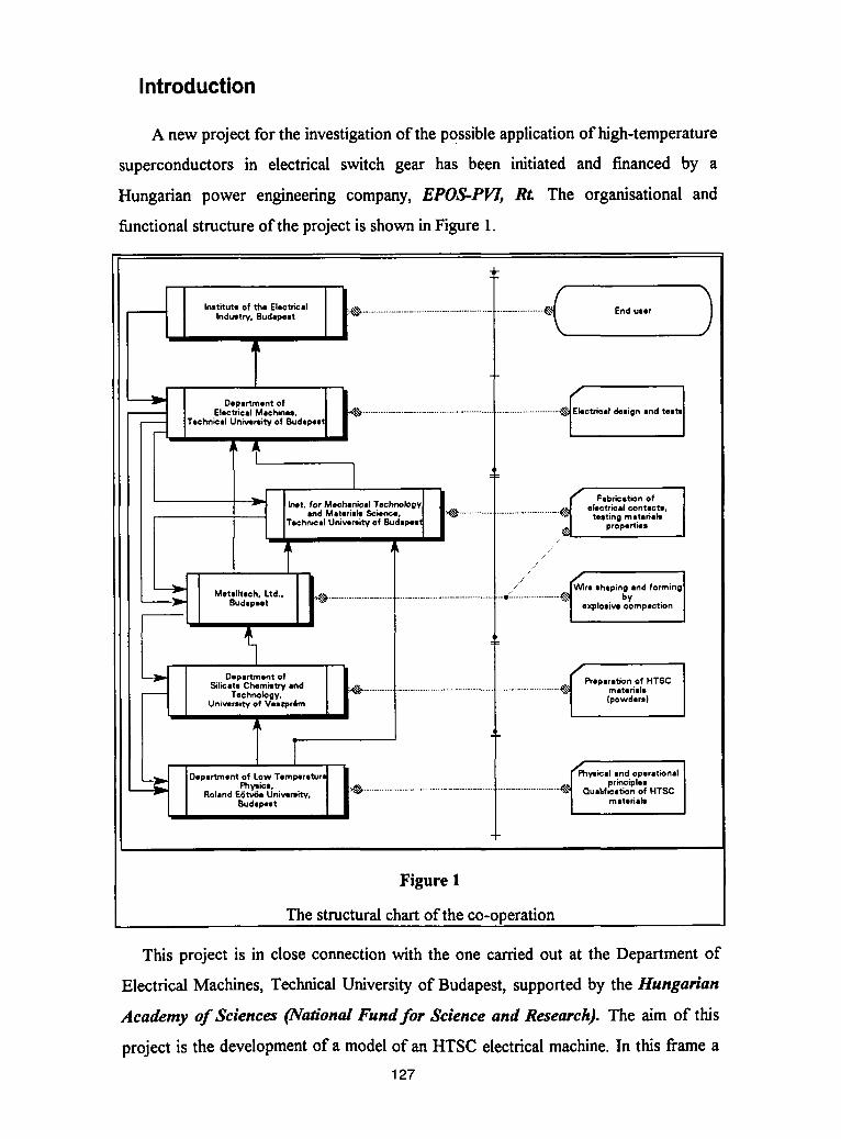
Introduction
A new projectfor the investigationof the POssibleapplicationof high-temperature
superconductors in electrical switch gear has been initiated and financed by a
Hungarianpower engineeringcompany, EPOS-PVI, Rt The organisationaland
functionalstructureof the projectis showninFigure1.
/- "xInstitute of the Electrical ..................._-_ End user |
Indultry, Budapest -\ J
O.--n,o, IElectrical Machines, ctrloal design and test=Technical UnivemiW of
Department ofSilk:eta Chemistry end Prspsrsticn of HTSCmstsriale
Technology, (powders)University of Veazpr6m
Figure 1
The structuralchartof the co-operation
This project is in close connectionwith the one carriedout at the Departmentof
ElectricalMachines,TechnicalUniversityof Budapest,supportedby the Hungarian
Academy of Sciences (National Fund for Science and Research). The aim of this
projectis the developmentof a model of an HTSC electricalmachine.In this framea127
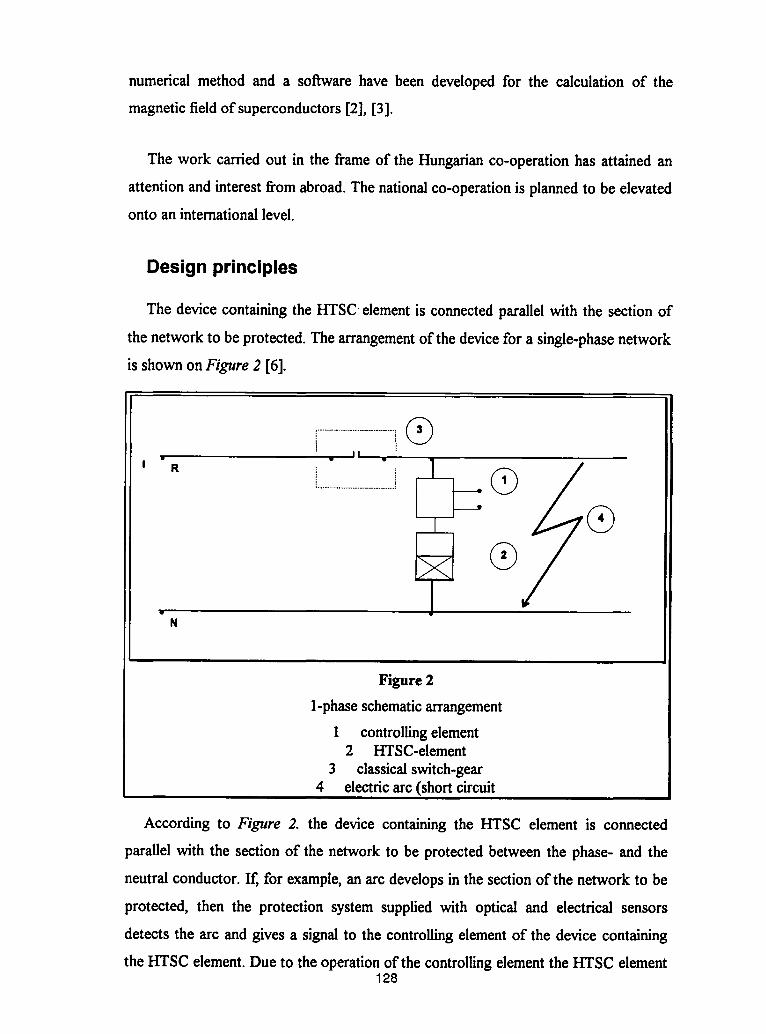
numerical method and a software have been developed for the calculation of the
magneticfieldof superconductors[2], [3].
The work carried out in the frame of the Hungarian co-operation has attained an
attention and interest from abroad. The nationalco-operation is planned to be elevated
onto an international level.
Design principles
The device containingthe HTSC element is connectedparallelwith the section of
the network to be protected. The arrangementof the devicefor a single-phasenetwork
is shown on Figure 2 [6].
• • II • ,I R
°N
Figure2
1-phaseschematicarrangement
1 controllingelement2 HTSC-element
3 classicalswitch-gear4 electricarc (shortcircuit
According to Figure 2. the device containingthe HTSC element is connected
parallelwith the section of the networkto be protectedbetween the phase- and the
neutralconductor.If, for example,an arc developsin the sectionof the networkto be
protected, then the protection system suppliedwith optical and electrical sensors
detects the arc and gives a signal to the controllingelementof the device containing
the HTSC element.Due to the operation of the controllingelement the HTSC element128
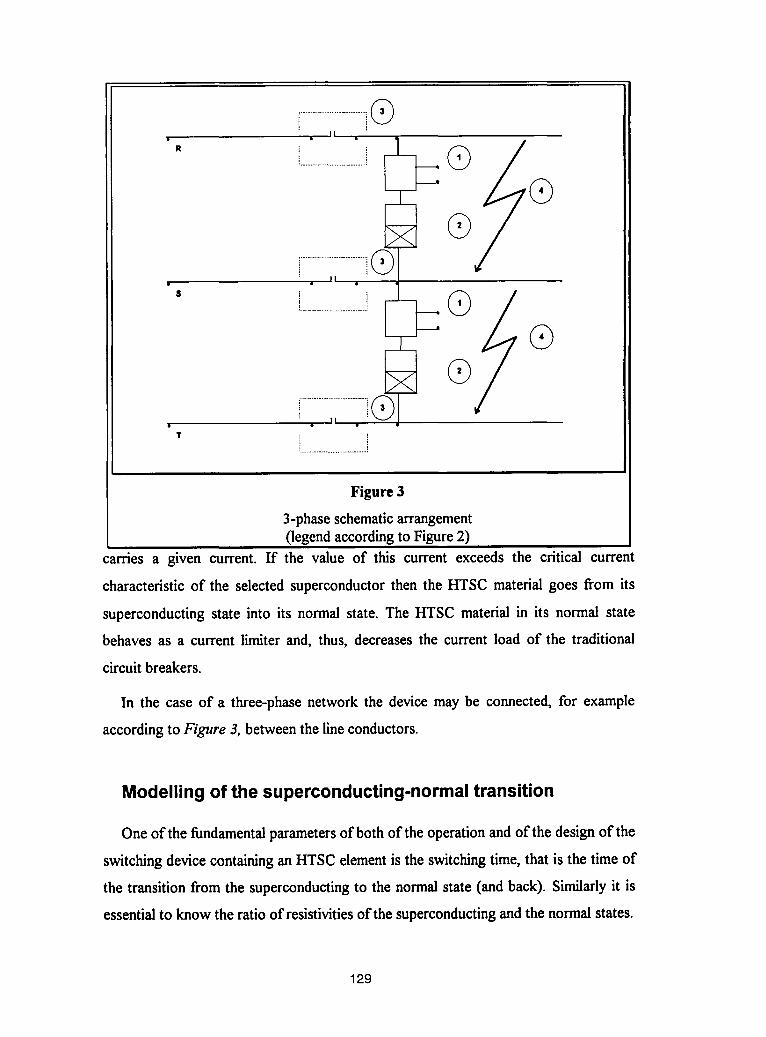
II
" ................................oo
II
Figure 3
3-phaseschematicarrangement(legendaccordingto Figure2)
carries a given current. If the value of this current exceeds the criticalcurrent
characteristicof the selected superconductorthenthe HTSC materialgoes from its
superconductingstate into its normal state. The HTSC materialin its normal state
behavesas a current limiter and, thus, decreasesthe currentload of the traditional
circuitbreakers.
In the case of a three-phase network the device may be connected, for example
according to Figure 3, betweenthe lineconductors.
Modellingof the superconducting-normaltransition
One of the fundamentalparametersof both of the operationand of the design of the
switchingdevice containingan HTSC elementis the switchingtime, that is the time of
the transition from the superconductingto the normalstate (and back). Similarlyit is
essentialto know the ratio of resistivitiesof the superconductingand the normalstates.
129
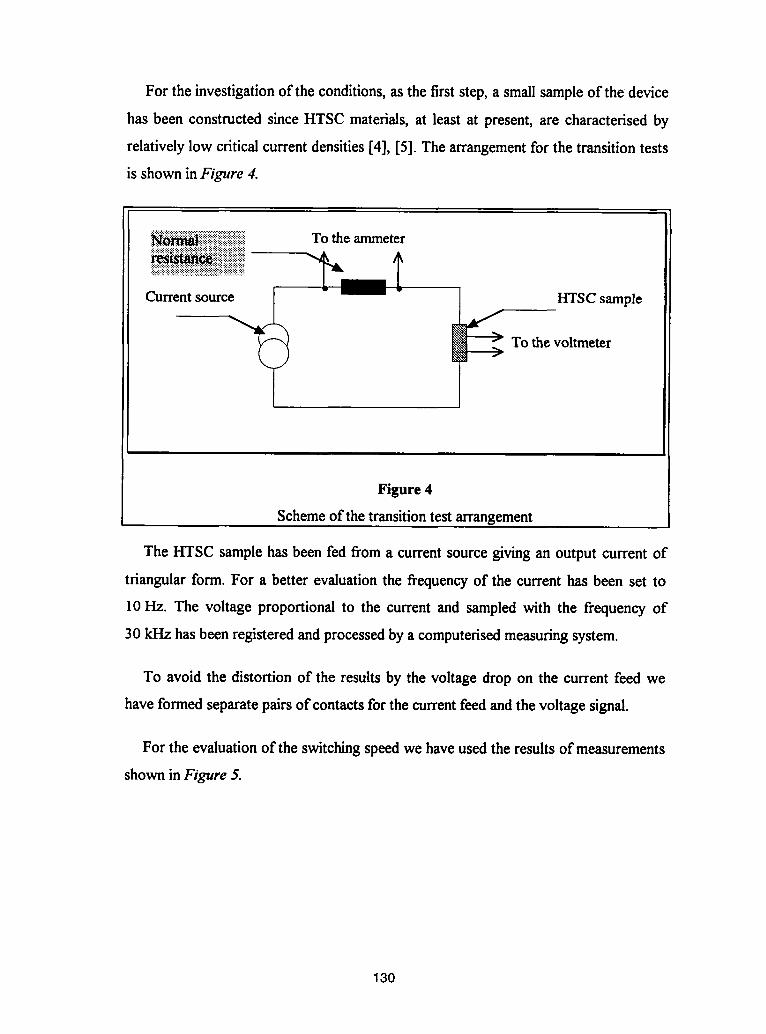
For the investigationof the conditions,as the firststep, a smallsampleof the device
has been constructedsince HTSC materials,at least at present, are characterisedby
relativelylow criticalcurrentdensities[4], [5]. Thearrangementforthe transitiontests
is shownin Figure 4.
_i_i_i_i_iiiiiiiiiiii_iiiililiiiiii To the ammeter
!iiiiiiiiiiiiiiiiiiiiiii_i_iiiiiiiiiiiiii!i!i_iiiiii_i
Currentsource HTSCsample
__ _ To thevoltmeter
Figure 4
Schemeof the transitiontest arrangement
The HTSC sample has been fed from a current source giving an output current of
triangular form. For a better evaluationthe frequency of the current has been set to
10Hz. The voltage proportional to the current and sampled with the frequency of
30 kHz has been registered and processed by a computerisedmeasuringsystem.
To avoid the distortion of the results by the voltage drop on the current feed we
haveformedseparatepairsof contactsfor the currentfeedand the voltage signal.
Forthe evaluationof the switchingspeedwe have usedthe resultsof measurements
shown inFigure 5.
130
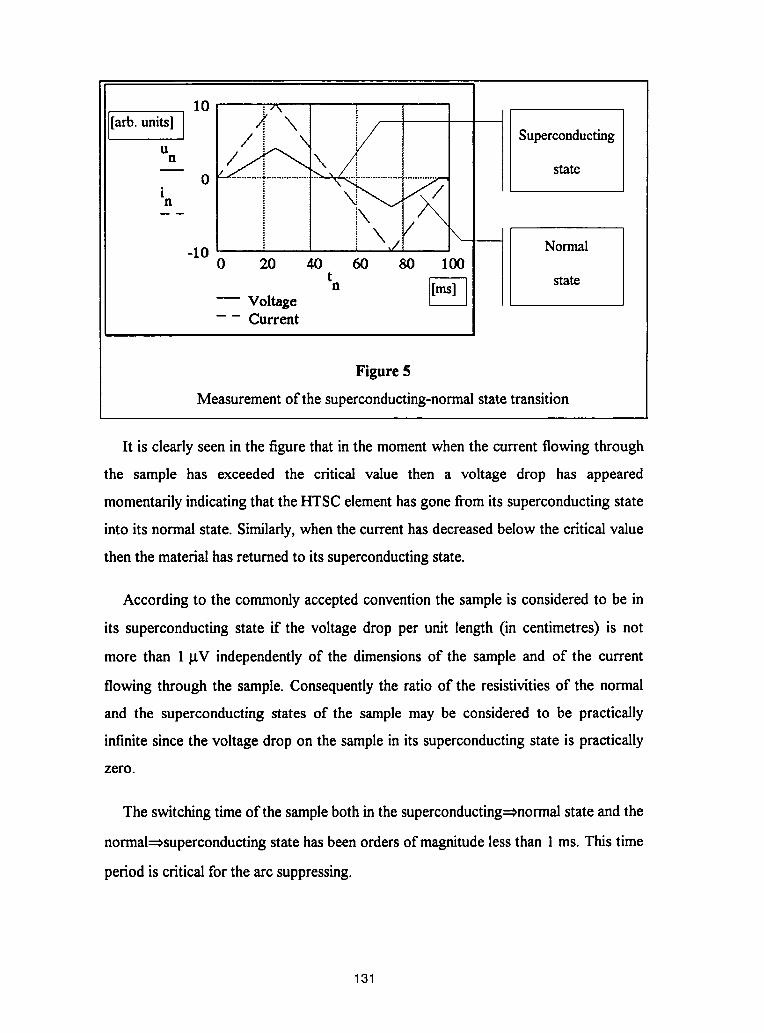
I0 _rx i
in 0 <! i\ /-I0 ! i _'I _----", Normal
0 20 40 60 80 I00tn _ , state
CELJVoltage-- Current
Figure5
Measurementof the superconducting-normalstatetransition
It is clearly seen inthe figure that inthe momentwhen the currentflowing through
the sample has exceeded the critical value then a voltage drop has appeared
momentarilyindicatingthatthe HTSCelementhasgone fromits superconductingstate
into its normalstate. Similarly,whenthe currenthasdecreasedbelow the criticalvalue
thenthe materialhasreturnedto itssuperconductingstate.
According to the commonlyacceptedconventionthe sample is considered to be in
its superconducting state if the voltage drop per unit length (in centimetres) is not
more than 1 l.tV independently of the dimensionsof the sample and of the current
flowing through the sample. Consequentlythe ratio of the resistivitiesof the normal
and the superconducting states of the sample may be considered to be practically
infinitesince the voltage drop on the samplein its superconducting state is practically
zero.
The switchingtime of the sampleboth inthe superconducting=normal state andthe
normal_superconducting state has been orders of magnitude lessthan 1 ms. This time
period is critical for the arc suppressing.
131
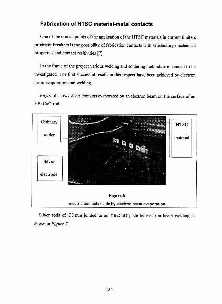
Fabricationof HTSC material-metalcontacts
One of the crucialpoints of the applicationof the HTSC materialsin current limiters
or circuit breakers is the possibilityof fabricationcontacts with satisfactorymechanical
properties and contact resitivities[7].
In the frame of the project various weldingand solderingmethods are planned to be
investigated.The first successfulresults in this respect have been achieved by electron
beam evaporation and welding.
Figure 6 shows silver contacts evaporatedby an electronbeam on the surface of an
YBaCuO rod.
Ordinary HTSC
solder material
Silver
electrode
Figure6
Electriccontactsmadebyelectronbeamevaporation
Silverrodsof _3 mmjointed to an YBaCuOplate by electronbeamweldingis
showninFigure7.
132
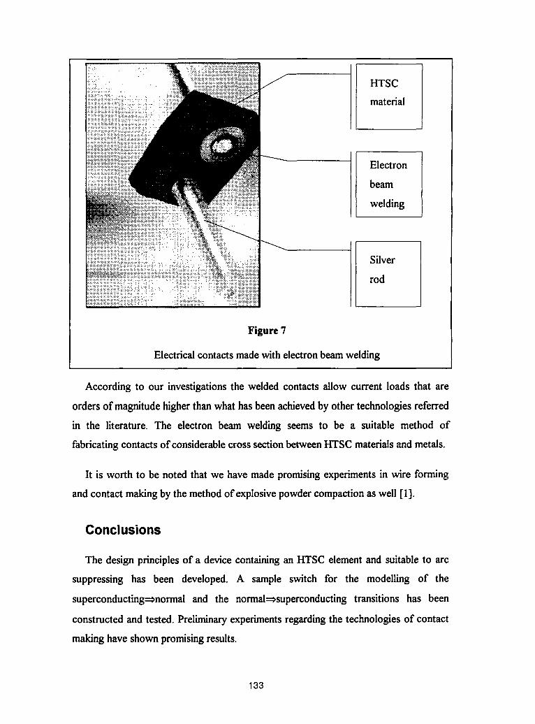
HTSC
material
Electron
beam
welding
Silver
rod
Figure7
Electricalcontactsmadewithelectronbeamwelding
Accordingto our investigationsthe welded contactsallow current loads that are
orders of magnitudehigherthanwhathasbeenachievedby othertechnologiesreferred
in the literature. The electron beam welding seems to be a suitable method of
fabricatingcontactsof considerablecross sectionbetweenHTSC materialsandmetals.
It is worth to be notedthatwe havemadepromisingexperimentsin wire forming
andcontact makingbythe methodof explosivepowdercompactionas well [1].
Conclusions
The designprinciplesof a devicecontainingan HTSCelementand suitableto arc
suppressing has been developed. A sample switch for the modelling of the
superconducting:=_normaland the normal=csuperconductingtransitions has been
constructedand tested.Preliminaryexperimentsregardingthe technologiesof contact
makinghave shown promisingresults.
133
References
[1] L. Bencze, A. Szalay, L Vajda:Fabricationof an HTSC Switch
Sensors and Actuators A, 41-42, p. 70-73, (1994), (EUROSENSORS VII).
[2] L Vajda,K. Kovfcs: Calculationof the LevitationForce of a High
Temperature Magnetic Bearing,
International Conferenceon ElectricalMachines,5-8 Sept, 1994.
[3] L Vajda,L. Z Mohdcsi, K.Kovtics:Modellingof the Superconductor for the
Application in High Temperature SuperconductingMagnetic Beating,
The 3rd Japan-HungaryJoint Seminaron AppliedElectromagneticsin
Materialsand ComputationalTechnology,Budapest, 10-13 July, 1994.
[4] L Kirschner: Requirementsand Results of High-To SuperconductingWire
and Tape Fabrication,
Applied Superconductivity,1, 10-12,.p. 1785-1789,1993.
[5] L Kirschner: HTSC Materials- Propertiesand Applications,
Research Report, Institute of the ElectricalIndustry, Budapest, 1994,
(In Hungarian).
[6] 1¢.Kovfcs: A Study on the ControllingMethods of HTSC Shunt Devices,
Research Report, Institute of the ElectricalIndustry, Budapest, 1994,
(In Hungarian).
[7] B. Palotts: A Study on the TechnologiesApplicablefor Making Contacts
Between HTSC Materialsand Metals,
Research Report, Institute of the ElectricalIndustry,Budapest, 1994,
(In Hungarian).
134

THIS PAGE INTENTIONALLY LEFT BLANK


Persistent Magnetic Fields
Chair. Dr. Roy Weinstein
STABILITY, MECHANICAL CONSIDERATIONS, AND AC LOSS IN HTSCMONOLITHS, COILS, AND WIRES
M. D. Sumption and E. W. Collings
Battelle Memorial Institute505 King Ave, Columbus, OH 43201, USA
Abstract
For monolithic high-Tc superconductors (HTSCs) calculations are presented of: (l) the initial flux jumpfield, H0, in melt-processed YBCO based on a field- and temperature dependent Jc, and (2) the radialand circumferential stresses in solid and hollow cylinders containing trapped magnetic flux. For modelmultifilamentary (MF) HTSC/Ag strands calculations are presented of: (1) the limiting filamentdiameters for adiabatic and dynamic stability, and (2) the hysteretic and eddy current components of ACloss. Again for MF HTSC/Ag composite strands the need for filamentary subdivision and twisting isdiscussed.
INTRODUCTION
Large-scale applications of high-Tc superconductors (HTSCs) stem not only from theirobviously high Tcs which offer the possibility of operation in liquid hydrogen, liquid nitrogenas well as refrigerated gases, but also from their high Hc2swhen high operating temperature isnot the primary consideration. The thermal properties central to stable conductor design arethermal conductivity, K(T), and specific heat, C(T). The former dominates at lowtemperatures and there dictates the choice of a dynamic stability criterion. Specific heat takesover at high temperatures where stability is controlled by adiabatic considerations. The muchhigher C(T) of materials at 77 K than at 4 K guarantees a much greater adiabatic flux-jumpstability. Several effects related to stability, while present in LTSC materials, are much moreprominent in HTSCs; for example, a much more pronounced ramp rate dependence of fluxjumping (in non-stabilized samples).I In the first section of this paper, the field dependence offlux jumping in large monoliths of HTSC, and its associated adiabatic and dynamic aspects,will be considered. In the next section we calculate the Lorentz-force induced mechanicalstresses that are present in flux-trapped solid cylinders of melt grown YBCO. We then go onto compare these results to those for hollow cylinders. The discussion on stability thenconcludes with a note on flux-jump- and cryo-stabilization of Ag-clad HTSC strands. Thepaper continues with a discussion of AC loss in multifilamentary HTSC/Ag composite strands.Using a model strand configuration, typical hysteretic and eddy current losses are comparedwith reference to practically attainable matrix resistivities and twist pitches. We conclude witha discussion of the particular properties of filamentary subdivision in HTSCs.
MAGNETIC STABILITY OF HTSC MONOLITHS
A well known expression for the initial flux jump field, is Hi0= "_{Tz3C(T)ATo},in which ATo =-J/(-dJ,./dT). In its more widely used form, in which ATo is replaced by (Tc-Tb),a number ofassumptions have been made: (1) Jc is linearly dependent on T, (2) Jc is field independent, and(3) the sample is isotropic. These assumptions are convenient, and have worked reasonably
138
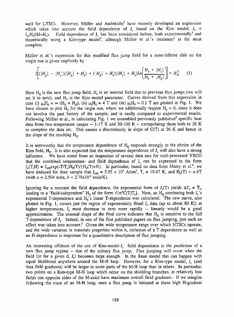
well for LTSCs. However, Mfiller and Andrikidis 2 have recently developed an expressionwhich takes into account the field dependence of Jc based on the Kim model, Jc =
J_oHo/(H+Ho). Field dependence of J_ has been considered before, both experimentally 3 andtheoretically using a Kim-type model 4, although Mfiller et al.'s treatment: is the mostcomplete.
Mfiller et al.'s expression for this modified flux jump field for a semi-infinite slab on the
virgin run is given implicitly by
_(,H_, - ,H I)(IH_[ + Ho) + (]Hcj[ + Ho)(IH , + Ho)Ln(_oo + IH'l !.gIH° [, = Hjo: (1)
Here H0 is the new flux jump field, He is an intemal field due to previous flux jumps (we willset it to zero), and I4-ois the Kim model parameter. Curves derived from this expression incase (i) i.@Io= ,,_(H_ -- Hi0), (ii) goHo= 4 T and (iii) goHo= 0.1 T are plotted in Fig. 1. Wehave chosen to plot H0 for the virgin run, where we additionally require He = 0, since it doesnot involve the past history of the sample, and is easily compared to experimental results.Following Mfiller et al., in calculating Fig. 1 we assembled previously published5 specific heatdata from two temperature ranges -- 1-17 K and 30-100 K -- extrapolating them both to 26 Kto complete the data set. This causes a discontinuity in slope of C(T) at 26 K and hence inthe slope of the resulting H0.
It is noteworthy that the temperature dependence of H0 responds strongly to the choice of theKim field, Ho. It is also expected that the temperature dependence of Jc will also have a stronginfluence. We have noted from an inspection of several data sets for melt-processed YBCOthat the combined temperature- and field dependence of Jo can be expressed in the formJ_(T,H) = J_0oexp(-T/T_)Ho(T)/{Ho(T)+H}. In particular, based on data from Maley et al.6, wehave deduced for their sample that J_oo= 5.92 x 10⁵ A/cm:, T, = 19.87 K, and Ho(T) = a-bT(with a = 2.504 tesla, b = 2.79x10"2tesla/K).
Ignoring for a moment the field dependence, the exponential form of J¢(T) yields ATo = T_,leading to a "field-independent" H0 of the form _]{x3C(T)T,}. Next, an H0 combining both Jc'sexponential T-dependence and Ho's linear T-dependence was calculated. The new curve, alsoplotted in Fig. 1, covers just the region of exponentially fitted J_ data (up to about 80 K); athigher temperatures, J_ must decrease to zero more rapidly -- linearly would be a goodapproximation. The unusual shape of the final curve indicates that H0 is sensitive to the fullT-dependence of J_. Indeed, in one of the first published papers on flux jumping, just such aneffect was taken into account) Given the wide temperature range over which HTSCs operate,and the wide variation in materials properties within it, inclusion of a T dependence as well asan H dependence is important for a quantitative description of flux jumping.
An interesting offshoot of the use of Kim-model-Jc field dependence is the prediction of anew flux jump regime -- that of the solitary flux jump. Flux jumping will occur when thefield (or for a given d, J¢) becomes large enough. In the Bean model this can happen withequal likelihood anywhere around the M-H loop. However, for a Kim-type model, Jc (andthus field gradients) will be larger in some parts of the M-H loop than in others. In particular,two points on a Kim-type M-H loop which occur on the shielding branches, at relatively lowfields (on opposite sides of the M-axis) have maximum overall field gradients. If we imaginefollowing the trace of an M-H loop, once a flux jump is initiated at these high H-gradient
139
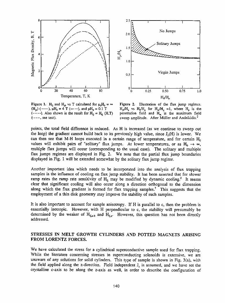
8 I I I 1 2.5 t I I I
[" /_ "-" 2.0 _ No Jumps _A 6- /
- / X\ 1.5/ ..-" ._=.o ._u.
4'-- • _,_
o°." \ 1.0-
/i I .*
•_ °.*"
.
2 / .."11 Virgin Jumps
//. o5- -o I I I w o ! I I
0 20 40 60 80 0 0.25 0.50 0.75 1.0
Temperature,T, K Ho/Hp
Figure 1. H0 and I-_ vs T calculatedfor _ = oo Figure 2. Illustrationof the flux jump regimes.(Hjo)(_), lat'Io= 4 T (----), and i.tl-Io = 0.1T Hjt-Ip vs I-Io/Hp for H_-Ip =1, where Hp is the(----). Alsoshownis the resultfor _ = _ (H,T) penetrationfield and _ is the maximum field(. • •., see text), sweepamplitude. After Mtillerand Andrikidis.2
points, the total field difference is reduced. As H is increased (as we continue to sweep outthe loop) the gradient cannot build back to its previously high value, since Jc(H) is lower. Wecan then see that M-H loops executed in a certain range of temperature, and for certain Hovalues will exhibit pairs of "solitary" flux jumps. At lower temperatures, or as Ho --_ oo,multiple flux jumps will occur (corresponding to the usual case). The solitary and multipleflux jumps regimes are displayed in Fig. 2. We note that the partial flux jump boundariesdisplayed in Fig. 1 will be extended somewhat by the solitary flux jump regime.
Another important idea which needs to be incorporated into the analysis of flux trappingsamples is the influence of cooling on flux jump stability. It has been asserted that for slowerramp rates the ramp rate sensitivity of _ may be modified by dynamic cooling.: It seemsclear that significant cooling will also occur along a direction orthogonal to the dimensionalong which the flux gradient is formed for flux trapping samples.7 This suggests that theemployment of a thin disk geometry may improve the stability of such samples.
It is also important to account for sample anisotropy. If H is parallel to c, then the problem isessentially isotropic. However, with H perpendicular to c, the stability will presumably bedetermined by the weaker of Hfi.__b and H_x. However, this question has not been directlyaddressed.
STRESSES IN MELT GROWTH CYLINDERS AND POTTED MAGNETS ARISINGFROM LORENTZ FORCES.
We have calculated the stress for a cylindrical superconductive sample used for flux trapping.While the literature concerning stresses in superconducting solenoids is extensive, we areunaware of any solutions for solid cylinders. This type of sample is shown in Fig. 3(a), withthe field applied along the z-direction. Field independent J_ is assumed, and we have set thecrystalline c-axis to be along the z-axis as well, in order to describe the configuration of
140
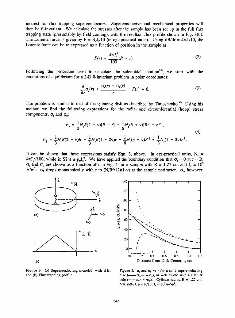
interest for flux trapping superconductors• Superconductive and mechanical properties willthen be 0-invariant. We calculate the stresses after the sample has been set up in the full fluxtrapping state (presumably by field cooling), with the resultant flux profile shown in Fig. 3(b).The Lorentz force is given by F = BrJJ10 (in cgs-practical units). Using dB/dr = 4rdJ10, theLorentz force can be re-expressed as a function of position in the sample as
F(r) ---4_'J._:(R - r). (2)100
Following the procedure used to calculate the solenoidal solutions'9, we start with theconditions of equilibrium for a 2-D 0-invariant problem in polar coordinates:
a or(r) - Go(r) + F(r) = 0. (3)"_rGr(r) * r
The problem is similar to that of the spinning disk as described by Timoshenko. ]° Using hismethod we find the following expressions for the radial and circumferential (hoop) stresscomponents, a, and (Se:
ar =-_cR(2 + v)[R - r] --_Nc(3 +v)[R2-r2],(4)
(3e---._VcR(2 .v)R- 13._NcR(1+2v)r--_Nc(3 .v)R 2 . 18-.N(1+3v)r2.
It can be shown that these expressions satisfy Eqn• 3, above. In cgs-practical units, N¢ =4rdc2/100,while in SI it is laoJc2. We have applied the boundary condition that cr = 0 at r = R.crr and (:reare shown as a function of r in Fig. 4 for a sample with R = 1.27 cm and Jc = 109A/m:. ,:so drops monotonically with r to (NcR2/12)(1-v)at the sample perimeter. _, however,
140 i I i I I
120 --
_ 16O-
r,_ :_ so-(a) a-b ti
"o
,,_ 6O- _ "..
a-b E _"_'".
2o- / --/0-- !
0.0 0.2 0.4 0.6 0.8 1.0 ! .2
(b) Distancefrom DiskCenter,r, cm
Figure 3. (a) Superconducting monolith with H|c, Figure 4. _, and _o vs r for a solid superconductingand (b) Flux trapping profile, disk (_G,,----Go), as well as one with a circular
hole (--.-- (s,,. .... ae). Cylinder radius, R = 1.27 cm;hole radius, a = R/10; J== lOSA/cm2.
141
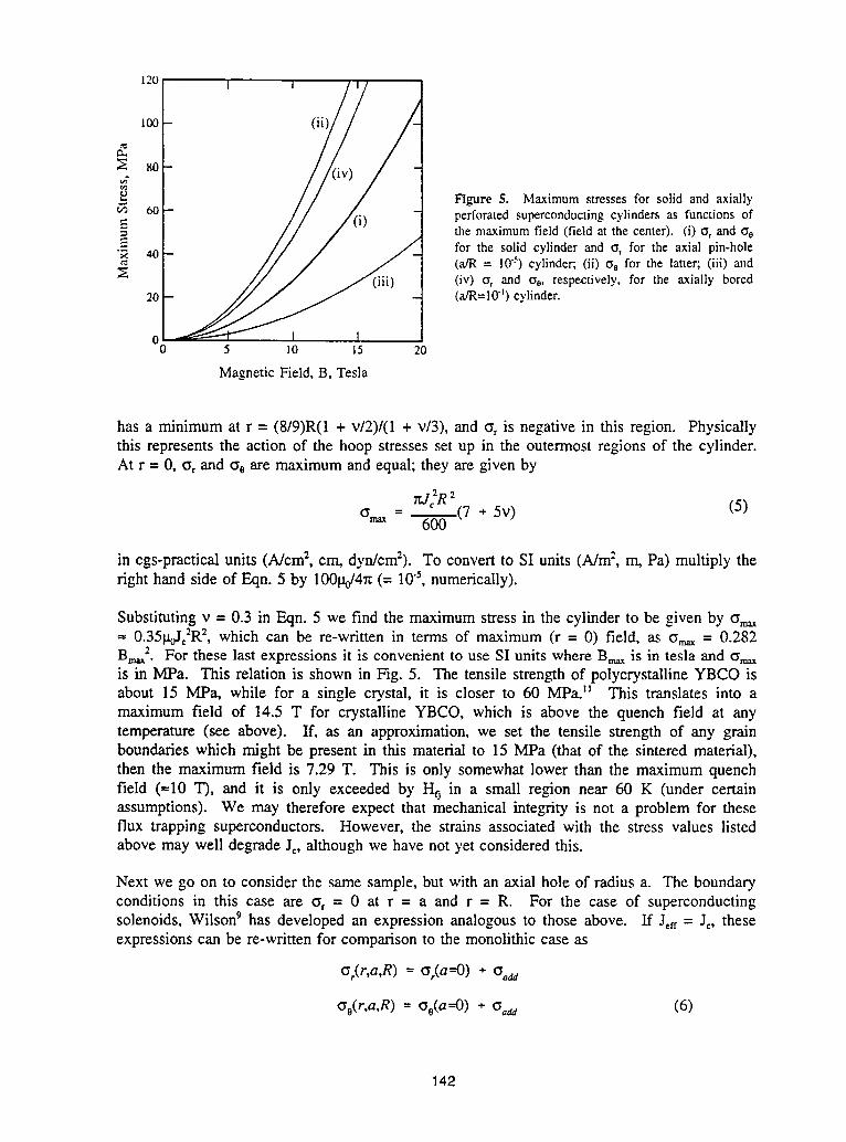
120 I I
log - (ii)e_
r_
s0-
Figure 5. Maximum stresses for solid and axially60 - perforated superconducting cylinders as functions of
= the maximum field (field at the center). (i) o, and oe- for the solid cylinder and o', for the axial pin-hole"_: 40 -= (a/R = 105) cylinder; (ii) _e for the latter; (iii) and
(iv) _, and Oe,respectively, for the axially bored20 - (a/R=10_) cylinder.
0 I I0 5 10 15 20
MagneticField,B, Tesla
has a minimum at r = (8/9)R(1 + v/2)/(1 + v/3), and g, is negative in this region. Physicallythis represents the action of the hoop stresses set up in the outermost regions of the cylinder.At r = 0, g, and ge are maximum and equal; they are given by
rd_R:_,(7 + 5v) (5)
g_= = 600
in cgs-practical units (A/cm:, cm, dyn/cm:). To convert to SI units (A/m:, m, Pa) multiply theright hand side of Eqn. 5 by 100po/4rt(= 105, numerically).
Substituting v = 0.3 in Eqn. 5 we find the maximum stress in the cylinder to be given by gm_x= 0.35BoJc"R:,which can be re-written in terms of maximum (r = 0) field, as gm_ = 0.282B_:. For these last expressions it is convenient to use SI units where B,,_ is in tesla and c_is in MPa. This relation is shown in Fig. 5. The tensile strength of polycrystalline YBCO isabout 15 MPa, while for a single crystal, it is closer to 60 MPaJ _ This translates into amaximum field of 14.5 T for crystalline YBCO, which is above the quench field at anytemperature (see above). If, as an approximation, we set the tensile strength of any grainboundaries which might be present in this material to 15 MPa (that of the sintered material),then the maximum field is 7.29 T. This is only somewhat lower than the maximum quenchfield (=10 T), and it is only exceeded by _ in a small region near 60 K (under certainassumptions). We may therefore expect that mechanical integrity is not a problem for theseflux trapping superconductors. However, the strains associated with the stress values listedabove may well degrade Jc, although we have not yet considered this.
Next we go on to consider the same sample, but with an axial hole of radius a. The boundaryconditions in this case are g_ = 0 at r = a and r = R. For the case of superconductingsolenoids, Wilson9 has developed an expression analogous to those above. If Jeff= J¢, theseexpressions can be re-written for comparison to the monolithic case as
g (r,a,R) = g (a--'O) + g_aa
ge(r,a'R) -- Go(a--0)+ g_aa (6)
142
where
c_aa= N(2 +v)_,g 1 - qr--i- - _(3 * v)a2 1 - q__
where q = 1 for c, and q = -1 for _o. In the above treatment, hollow cylinders and pottedBi:HTSC/Ag pancake coils give the same results as solenoids. Plots for _, and _e for a =R/10 are shown in Fig. 4 for comparison to the results for the monolith. We can see that thepresence of the hole decreases at, but increases _o. In Fig. 5, curves of maximum _ and _e(for a given internal B) are shown as a function of the internal field, B (which is assumedconstant throughout the hole) and compared to the monolith results. For the case with thecenter hole, oe still maximizes at the inner boundary, but _ maximizes somewhere within thestructure, as shown in Fig. 4. As we can see in Figs. 4 and 5, with the introduction of a hole,_r becomes equal to or less than its counterpart for the monolith, while o e becomes equal to orgreater than its counterpart for the monolith. Thus, as shown in Fig. 5, in the limit of a --->0,the maximum in _,_oleis equal to the maximum value of _,_o,o, while the maximum in _e.hol_istwice that of _O.mo,o-This agrees with the idea of stress enhancement around holes typicallyfound in mechanics.
STABILITY IN MULTIFILAMENTARY STRANDS
Superconducting wires (strands) are generally produced in multifilamentary (MF) form. Low-T¢ strands for accelerator magnet applications, for example, often consist of many thousands offilaments (e.g. 5,000 to 40,000); they are small in diameter to provide stability and lowhysteretic loss, and twisted together to reduce eddy current loss to some fraction of thehysteretic value. As we shall see, in HTSC strands filamentary subdivision serves some of theabove functions but also some additional ones. For practical reasons the number of filamentstends to be smaller and consequently the twisting requirement is less stringent. The firstrequirement in MF strand design is to prevent flux jumping. For NbTi, filaments smaller thanabout 100 lam in diameter are immune to it. This is also approximately true for HTSC strandsat 4 K. But at 77 K they are adiabatically flux jump stable in diameters as large as severalcm. In general, requirements other than stability tend to dictate the choice of filamentdiameter. For LTSCs these are low magnetization and low AC loss. For HTSCs thedominating requirement has to do with grain alignment. For example in the Ag-clad Bi:HTSCwires, alignment seems to take place when the superconductor "thickness" is less than about 50lam. The following account demonstrates that this is certainly compatible with flux jumpstability.
In calculating the filament diameter requirements for flux jump stability two alternative criteriamay be applied -- the adiabatic and the dynamic. The former dominates if the heat capacity ishigh and cryocooling can be ignored; in the dynamic case heat conduction to a cryogen bathmust be invoked. The maximum filament diameter under the adiabatic criterion (based on aslab calculation1:"p.134)in c.g.s, units is
rid= _ 109(3)C(T)ATo/J(T,H) (7)
143
The dynamic criterion (based on a cylinder calculation_:'p.156)yields
-- 8Isc /Jc(r,m (8)"' flag X
In these equations C(T) and Ksc are the heat capacity and thermal conductivity, respectively,of the superconductor (SC), PAgis the silver stabilizer resistivity, _, is the volume fraction ofSC in the composite (herein 0.5) and ATo - J/(-dJ/dT).
The equations can be evaluated using the appropriate cryophysical property data.
Cryophysical Property Data
The temperature dependencies of the relevant thermal and electrical properties of YBCO andcopper (for model calculations of the stabilities of YBCO/Cu composites) were previouslylisted.5 In what follows we repeat some of the earlier calculations but for the more realisticcase of YBCO/Ag, since the following data for Ag has recently become available. In addition,for ATo and Jc(T,H) we draw on new data from Maley et al.6 As indicated earlier the Jc(T,H)of melt processed YBCO (T¢ = 90 K) is well described by an exponentially decreasingtemperature dependence to about 80 K of the form (5.92 x 10⁵ A/cm2)exp(-T/Ts) with Ts =19.87 K, combined with a Kim-type field dependence quotient of the form H0(T)/{Ho(T)+H}in which Ho(T) = a-bT (a = 2.504 tesla, b = 2.79x10² tesla/K). Above about 80 K, J¢ dropslinearly to zero at Tc. Thus at 4 K, ATo = 1", = 19.87 K; while at 77 K, ATo may beapproximated by the usual (Tc-Tb)= 13 K.
Electrical Resistivity of the Silver Stabilizer: Drawn wires of 99.99% Ag and an Ag-0.1%A1 alloy were annealed in air for 24h/840°C during which they became charged withoxygen and the alloy internally oxidized to Ag plus AI203. Their measured resistivities were:Ag: P4K= 9.27 n_cm, P77z= 290.56 nf_cm; Ag+Ox: P4K= 247.42 nf2cm, P77z= 624.51nD.cm.
Magnetoresistance of Silver: The magnetoresistivity of Ag over the temperature range 4.2-159 K.has been measured by Iwasa et al._3 Based on their data we have deduced that at 4.2K a field of 5 T adds to Ag a resistivity of 11.61 nff2cm. In the stability calculations weassume this to be temperature independent and add it to both the 4.2 K and 77 K resistivitiesto take into account the effect of a 5 T field.
Maximum Filament Diameters for Flux Jump Stability
Based on Eqns. (8) and (9) the maximum filament diameters for adiabatic and dynamic fluxjump stability, respectively, are as depicted in Table 1. The table indicates that at 4 K thedynamic criterion applied to the pure-Ag-stabilized composite guarantees the stability offilaments of the size expected in practice (certainlyless than 100 pro). Some dynamic stabilityis lost when oxide-strengthened Ag is employed, in which case the adiabatic and dynamicresults are similar. At 77 K both YBCO and YBCO/Ag are "overstable" from both adiabaticand dynamic standpoints; filaments thicker than those that would ever be encountered inpractice are immuneto flux jumping.
144
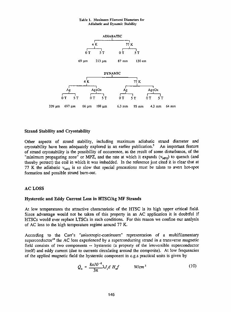
Table I. Maximum Filament Diameters for
Adiabatic and Dynamic Stability
ADIABATICI
I |4K 77K
I I0T 5T 0T 5T
69 I.tm 213 I.tm 87 mm 130 cm
DYNAMICI
I i4K 77K
i II I [ i
Ag _ Ag0T 5T 0T 5T 0T 5T 0T 5T
339 [am 697 I.tm 66 I.tm 198 I.tm 6.3 rnm 93 mm 4.3 mm 64 mm
Strand Stability and Cryostability
Other aspects of strand stability, including maximum adiabatic strand diameter andcryostability have been adequatelyexplored in an earlier publication.5 An importantfeatureof strandcryostability is the possibility of occurrence,as the result of some disturbance,of the"minimum propagating zone" or MPZ, and the rate at which it expands (VMr_ to quench (andthereby protect) the coil in which it was imbedded. In the referencejust cited it is clear that at77 K the adiabatic VMpz is SOslow that special precautions must be taken to avert hot-spotformation and possible strand burn-out.
AC LOSS
Hysteretic and Eddy Current Loss in HTSC/Ag MF Strands
At low temperaturesthe attractivecharacteristicof the HTSC is its high upper critical field.Since advantage would not be taken of this property in an AC application it is doubtful ifHTSCs would ever replaceLTSCs in such conditions. For this reason we confine our analysisof AC loss to the high temperatureregime around77 K.
According to the Carr's "anisotropic-continuum" representation of a multifilamentarysuperconductor_4the AC loss experienced by a superconducting strand in a transverse magneticfield consists of two components -- hysteretic (a property of the irreversible superconductoritself) and eddy current (due to currents circulating around the composite). At low frequenciesof the applied magnetic field the hysteretic component in c.g.s practical units is given by
Qh-- 8x1043rt Lied H,_ Wlcm3 (10)
145
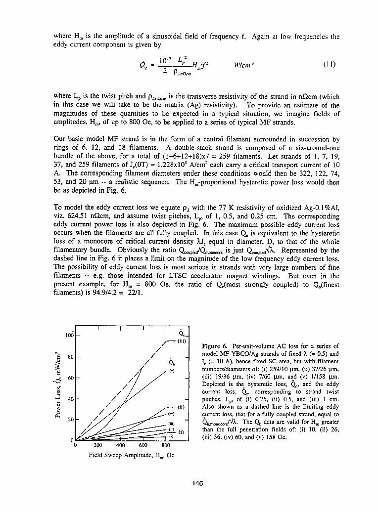
where Hmis the amplitude of a sinusoidal field of frequency f. Again at low frequencies theeddy current component is given by
(2,= 1o-7 H,."f W/cm3 (11)2 P_a,,
where Lp is the twist pitch and p._m,, is the transverse resistivity of the strand in n_cm (whichin this case we will take to be the matrix (Ag) resistivity). To provide an estimate of themagnitudes of these quantities to be expected in a typical situation, we imagine fields ofamplitudes, Hm,of up to 800 Oe, to be applied to a series of typical MF strands.
Our basic model MF strand is in the form of a central filament surrounded in succession byrings of 6, 12, and 18 filaments. A double-stack strand is composed of a six-around-onebundle of the above, for a total of (1+6+12+18)x7 = 259 filaments. Let strands of 1, 7, 19,37, and 259 filaments of Jc(0T) = 1.228x10⁴A/cm'-each carry a critical transport current of 10A. The corresponding filament diameters under these conditions would then be 322, 122, 74,53, and 20 lain -- a realistic sequence. The Hm-proportional hysteretic power loss would thenbe as depicted in Fig. 6.
To model the eddy current loss we equate p± with the 77 K resistivity of oxidized Ag-0.1%A1,viz. 624.51 n_cm, and assume twist pitches, Lp, of 1, 0.5, and 0.25 cm. The correspondingeddy current power loss is also depicted in Fig. 6. The maximum possible eddy current lossoccurs when the filaments are all fully coupled. In this case Q_ is equivalent to the hystereticloss of a monocore of critical current density Lie equal in diameter, D, to that of the wholefilamentary bundle. Obviously the ratio Q,o_pldQ_,o_o_is just Qcoupl_4_..Represented by thedashed line in Fig. 6 it places a limit on the magnitude of the low frequency eddy current loss.The possibility of eddy current loss is most serious in strands with very large numbers of finefilaments -- e.g. those intended for LTSC accelerator magnet windings. But even in thepresent example, for _ = 800 Oe, the ratio of Q,(most strongly coupled) to Qh(finestfilaments) is 94.9/4.2 = 22/1.
I I I Ilo6
/_ (iii)/ Figure 6. Per-unit-volumeAC lossfor a seriesof
80 - / _ modelMF YBCO/Ag strandsof fixed2.(= 0.5) and/ Qh Ic (= 10 A), hencefixed SC area,but with filament
(v_ numbers/diametersof: (i) 259/10lain,(ii) 37/26l.tm,._ 60 (iii) 19/36I.tm,(iv) 7/60 _tm,and (v) 1/158I.tm.
/ Depicted is the hysteretic loss, Qh, and the eddy/ current loss, _, correspondingto strand twist
40 / pitches,Lp, of (i) 0.25, (ii) 0.5, and (iii) 1 cm./ Also shownas a dashedline is the limiting eddyo / current loss, that for a fully coupled strand, equal to
20 Qn.monoco_/_/_..The Qhdataare validfor Hmgreater(ii)(i) than the full penetrationfields of: (i) 10, (ii) 26,
0 (iii) 36, (iv) 60, and (v) 158Oe.0 200 400 600 800
Field SweepAmplitude,Hm,Oe
146
Twist Pitch, Matrix Resistivity, and Filament-Diameter Considerations
Based on the above physical-propertydata set the ratio QJQh is just 0.7681(Lp'/d.m)Hmwhichemphasizes the importance of reducing both twist pitch and filament diameter in theminimization of eddy current loss. For equal loss at Hm = 500 Oe, for example, d,m = 384
Lpcm2. When d = 24 pm this calls for a twist pitch of 0.25 cm. For the strand diameter D =d_(N/k) = 0.46 mm considered in these examples, this corresponds to a pitch/diameter ratio of5.5/1 which would be quite tight even for a NbTi/Cu strand. The alternative to reducing Lp is
increasing the matrix resistivity.
If sufficient twist or resistivity cannot be introduced, full electrical advantage cannot be taken
of multi filamentary subdivision, especially since fine filaments often turn out to beinterconnected by "bridges". Nevertheless there are other advantages to be considered: (1)Reduction of filament diameter aids in HTSC grain alignment. (2) The ductile interfilamentary
matrix with its crack-stopping potential can be expected to contribute a higher strain toleranceto the finer-filament composite; in which case even bridging may be an advantage.
REFERENCES
1. S.W. Hsu, K. Chen, and W.H. Lee, "Temperature and Field Sweeping Rate Dependence of FluxJumps in a Melt-Textured YBa2Cu3OT.xSuperconductor" 75, 799-803 (1990).
2. K.-H. Mtiller and C. Andrikidis, "Flux Jumps in Melt-Textured Y-Ba-Cu-O", Phys. Rev. B. 49,1294-1306 (1994).
3. R. Haneox, "The Superconductivity of Sintered Nb3Sn at Temperatures Above 4.2 K", Appl.Phys. Lett. 7, 138-139 (1965).
4. J. Sosnowski, "Influence of Magnetic History on Flux Jump Fields", J. Appl. Phys. 59, 4189-4191 (1986).
5. E.W. Collings, "Conductor Design with High-To Ceramics: A Review", Advances inSuperconductivity-H, ed. by T. Ishiguro and K. Kajimura, (Springer-Verlag, 1990) pp. 327-333.
6. P.J. Kung, M.P. Maley, M.E. McHenry, J.O. Willis, J.Y. Coulter, M. Murakami, and S. Tanaka,"Magnetic Hysteresis and Flux Creep of Melt-Powder-Melt-Growth YBa2Cu307 Super-conductors", Phys. Rev. B. 46, 6427-6434 (1992).
7. M. Chiba, T. Ogasawara, N. Miyazawa, S. Ban, et al, "The Magnetic Stability of Face-CooledComposite Tape Superconductors", IEEE Trans. Magn. 27, 1656-1659 (1991).
8. H. Brechna, Superconducting Magnet Systems, (Springer Verlag, NY, 1973) pp. 139-142; seealso H. Brechna, "Superconducting Magnets", in Superconducting Maehine_ and Devices,Large Systems Applications, ed. by S. Foner and B. Schwartz, NATO Advanced Study Series,(Plenum Press, NY, 1974) pp. 162-165.
9. M.N. Wilson, Superconducting Magnets, (Oxford, NY, 1983) pp. 41-46.10. S. Timoshenko and J.N. Goodier, Theory of Elasticity, (McGraw Hill, NY, 1951), pp. 69-71.11. K. Salama, private communication, 1994.12. E.W. Collings, Applied Superconductivity, Metallurgy and Physics of Titanium Alloys,
Volume 2, (Plenum Press, NY, 1986).13. Y. Iwasa, E.J. McNiff, R.H. Bellis, and K. Sato, "Magnetoresistance of Silver over Temperature
Range 4.2 - 159 K", Cryogenics 33, 836-838 (1993).14. W.J. Cart Jr., AC Loss and Macroscopic Theory of Superconductors, (Gordon and Breach,
NY, 1983) p. 348.
147
Presented at the World Congress on Superconductivity IV, June 27-July 1, '94, Orlando/FL,USA.
ASPECTS OF PASSIVE MAGNETIC LEVITATION BASEDON HIGH-ToSUPERCONDUCTING YBCO THIN FILMS
P. SchOnhuber*and F. C. MoonMechanical and Aerospace Engineering, Cornell University,
Ithaca, NY 14853, USA.
Abstract - Passive magnetic levitation systems reported in the past were mostly confinedto bulk superconducting materials. Here we present fundamental studies on magneticlevitation employing cylindrical permanent magnets floating above high-Tosuperconducting YBCO thin films (thickness about 0.3 l,tm). Experiments included freefloating rotating magnets as well as well-established flexible beam methods. By means ofthe latter, we investigated levitation and drag force hysteresis as well as magneticstiffness properties of the superconductor-magnet arrangement. In the case of verticalmotion of the magnet, characteristic high symmetry of repulsive (approaching) andattractive (withdrawing) branches of the pronounced force-displacement hysteresis couldbe detected. Achievable force levels were low as expected but sufficient for levitation ofpermanent magnets. With regard to magnetic stiffness, thin films proved to showstiffness-force ratios about one order of magnitude higher than bulk materials.
Phenomenological models support the measurements. Regarding the magnetichysteresis of the superconductor, the Irie-Yamafuji model was used for solving theequation of force balance in cylindrical coordinates allowing for a macroscopicdescription of the superconductor magnetization. This procedure provided goodagreement with experimental levitation force and stiffness data during vertical motion.For the case of (lateral) drag force basic qualitative characteristics could be recovered,too. It is shown, that models based on simple asymmetric magnetization of thesuperconductor describe well asymptotic transition of drag forces after the change of themagnet motion direction. Virgin curves (starting from equilibrium, i.e. symmetricmagnetization) are approximated by a linear approach already reported in literature, only.
This paper shows that basic properties of superconducting thin films allow fortheir application to magnetic levitation or - without need of levitation forces, e.g.microgravity - magnetic damping devices.
*onleavefromTechnicalUniversityVienna,Gusshausstr.27/351,A - 1040Vienna,Austria.
148
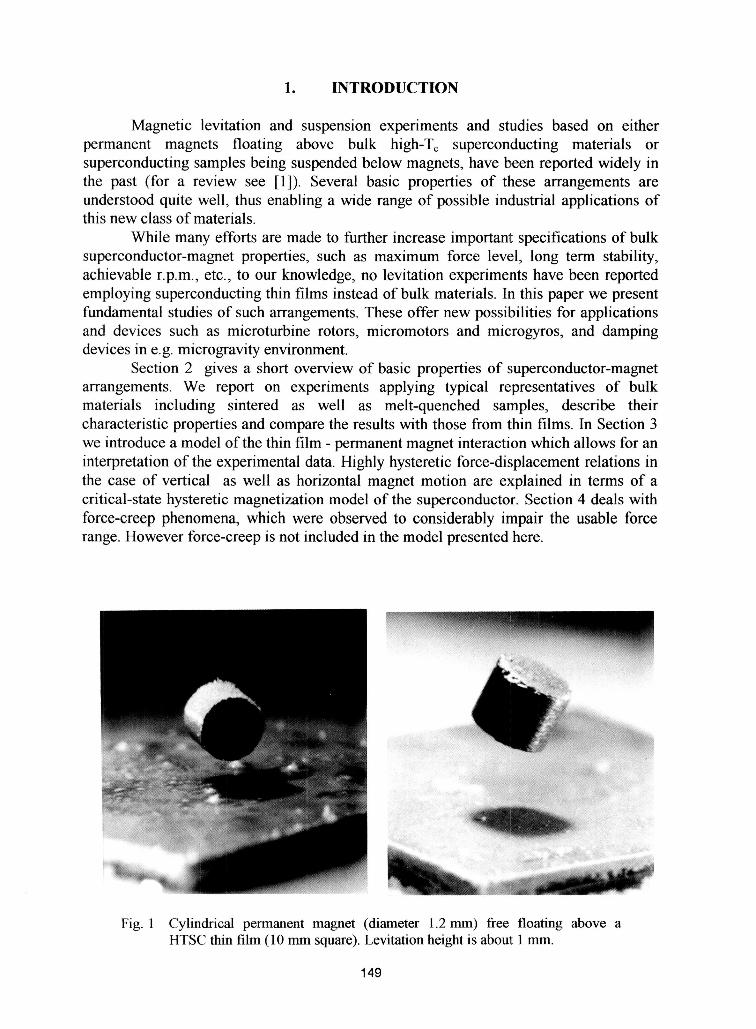
1. INTRODUCTION
Magnetic levitation and suspension experiments and studies based on eitherpermanent magnets floating above bulk high-To superconducting materials orsuperconducting samples being suspended below magnets, have been reported widely inthe past (for a review see [1]). Several basic properties of these arrangements areunderstood quite well, thus enabling a wide range of possible industrial applications ofthis new class of materials.
While many efforts are made to further increase important specifications of bulksuperconductor-magnet properties, such as maximum force level, long term stability,achievable r.p.m., etc., to our knowledge, no levitation experiments have been reportedemploying superconducting thin films instead of bulk materials. In this paper we presentfundamental studies of such arrangements. These offer new possibilities for applicationsand devices such as microturbine rotors, micromotors and microgyros, and dampingdevices in e.g. microgravity environment.
Section 2 gives a short overview of basic properties of superconductor-magnetarrangements. We report on experiments applying typical representatives of bulkmaterials including sintered as well as melt-quenched samples, describe theircharacteristic properties and compare the results with those from thin films. In Section 3we introduce a model of the thin film - permanent magnet interaction which allows for aninterpretation of the experimental data. Highly hysteretic force-displacement relations inthe case of vertical as well as horizontal magnet motion are explained in terms of acritical-state hysteretic magnetization model of the superconductor. Section 4 deals withforce-creep phenomena, which were observed to considerably impair the usable forcerange. However force-creep is not included in the model presented here.
Fig. 1 Cylindrical permanent magnet (diameter 1.2mm) free floating above aHTSC thin film (10 mm square). Levitation height is about 1mm.
149
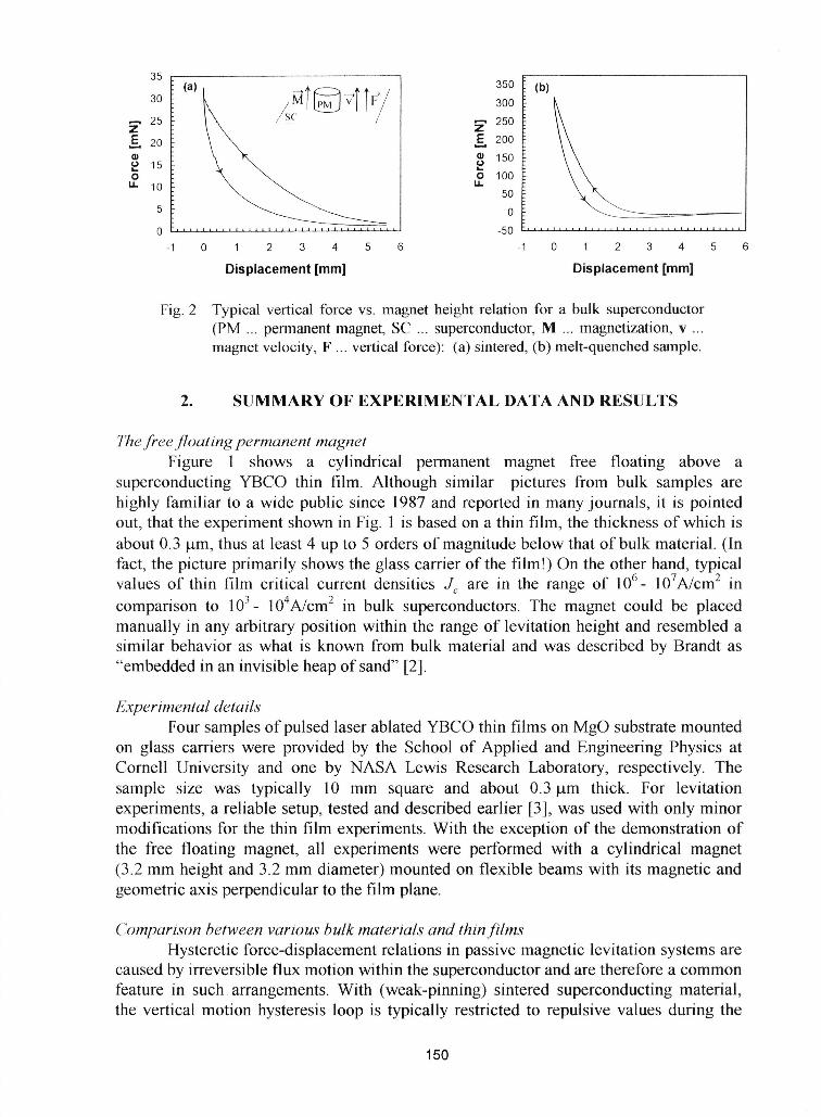
35(a) 350 (b)
30 ! 300
_ -z zI= 20 I= 200
• 15015
o o lOOu. 10 u.
5O
5 0
0 .................................. -50 ..................................-1 0 1 2 3 4 5 6 -1 0 1 2 3 4 5 6
Displacement [mm] Displacement [ram]
Fig. 2 Typical vertical force vs. magnet height relation for a bulk superconductor(PM ... permanent magnet, SC ... superconductor, M ... magnetization, v ...magnet velocity, F ... vertical force): (a) sintered, (b) melt-quenched sample.
2. SUMMARY OF EXPERIMENTAL DATA AND RESULTS
The free floating permanent magnetFigure 1 shows a cylindrical permanent magnet free floating above a
superconducting YBCO thin film. Although similar pictures from bulk samples arehighly familiar to a wide public since 1987 and reported in many journals, it is pointedout, that the experiment shown in Fig. 1 is based on a thin film, the thickness of which isabout 0.3 lam, thus at least 4 up to 5 orders of magnitude below that of bulk material. (Infact, the picture primarily shows the glass carrier of the film T)On the other hand, typicalvalues of thin film critical current densities .1c are in the range of 106- 107A/cm 2 incomparison to 103- 104A/cm2 in bulk superconductors. The magnet could be placedmanually in any arbitrary position within the range of levitation height and resembled asimilar behavior as what is known from bulk material and was described by Brandt as"embedded in an invisible heap of sand" [2].
Experimental detailsFour samples of pulsed laser ablated YBCO thin films on MgO substrate mounted
on glass carriers were provided by the School of Applied and Engineering Physics atCornell University and one by NASA Lewis Research Laboratory, respectively. Thesample size was typically 10 mm square and about 0.3 _am thick. For levitationexperiments, a reliable setup, tested and described earlier [3], was used with only minormodifications for the thin film experiments. With the exception of the demonstration ofthe free floating magnet, all experiments were performed with a cylindrical magnet(3.2 mm height and 3.2 mm diameter) mounted on flexible beams with its magnetic andgeometric axis perpendicular to the film plane.
Comparison between various bulk materials and thin filmsHysteretic force-displacement relations in passive magnetic levitation systems are
caused by irreversible flux motion within the superconductor and are therefore a commonfeature in such arrangements. With (weak-pinning) sintered superconducting material,the vertical motion hysteresis loop is typically restricted to repulsive values during the
150
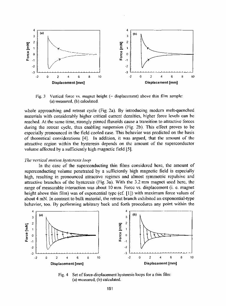
4 4(a) (b)3 3
,--, 2 ,-_ 2Z ZE 1 E 1
p o p 0O Ou. -1 u. -1
-2 -2
-3 i i i i i t i i J i , _ , , , i , , , I , , , -3 , , , , , , , i i i i i , , , i , , , i i i a
-2 0 2 4 6 8 10 -2 0 2 4 6 8 10
Displacement [mm] Displacement [mm]
Fig.3 Verticalforce vs. magnetheight (= displacement)above thin film sample:(a)measured,(b).calculated.
whole approaching and retreat cycle (Fig. 2a). By introducing modem melt-quenchedmaterials with considerably higher critical current densities, higher force levels can bereached. At the same time, strongly pinned fluxoids cause a transition to attractive forcesduring the retreat cycle, thus enabling suspension (Fig. 2b). This effect proves to beespecially pronounced in the field cooled case. This behavior was predicted on the basisof theoretical considerations [4]. In addition, it was argued, that the amount of theattractive region within the hysteresis depends on the amount of the superconductorvolume affected by a sufficiently high magnetic field [5].
The vertical motion hysteresis loopIn the case of the superconducting thin films considered here, the amount of
superconducting volume penetrated by a sufficiently high magnetic field is especiallyhigh, resulting in pronounced attractive regimes and almost symmetric repulsive andattractive branches of the hysteresis (Fig. 3a). With the 3.2 mm magnet used here, therange of measurable interaction was about 10 mm. Force vs. displacement (i. e. magnetheight above thin film) was of exponential type (cf. [1]) with maximum force values ofabout 4 mN. In contrast to bulk material, the retreat branch exhibited an exponential-typebehavior, too. By performing arbitrary back and forth procedures any point within the
4 4
3 (a) 3 (b)
0
u. -1 _ -1
-2 -2
-2 0 2 4 6 8 10 -2 0 2 4 6 8 10
Displacement [ram] Displacement [ram]
Fig. 4 Set of force-displacement hysteresis loops for a thinfilm:(a) measured, (b) calculated.
151
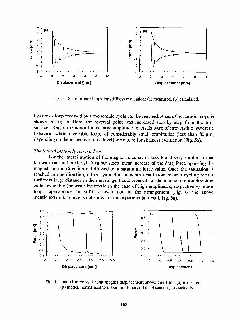
4 4
(a) _ (b)
3 3
2 _ 2Z Z
_ o _ o
° °_- -1 _- -1
-2 -2
-2 0 2 4 6 8 10 -2 0 2 4 6 8 10
Displacement [mm] Displacement [ram]
Fig. 5 Set of minor loops for stiffness evaluation: (a) measured, (b) calculated.
hysteresis loop received by a monotonic cycle can be reached. A set of hysteresis loops isshown in Fig. 4a. Here, the reversal point was increased step by step from the filmsurface. Regarding minor loops, large amplitude reversals were of irreversible hystereticbehavior, while reversible loops of considerably small amplitudes (less than 80 Hm,depending on the respective force level) were used for stiffness evaluation (Fig. 5a).
The lateral motion hysteresis loopFor the lateral motion of the magnet, a behavior was found very similar to that
known from bulk material. A rather steep linear increase of the drag force opposing themagnet motion direction is followed by a saturating force value. Once the saturation isreached in one direction, rather symmetric branches result from magnet cycling over asufficient large distance in the mm range. Local reversals of the magnet motion directionyield reversible (or weak hysteretic in the case of high amplitudes, respectively) minorloops, appropriate for stiffness evaluation of the arrangement (Fig. 6, the abovementioned initial curve is not shown in the experimental result, Fig. 6a).
08 12 [ (b)
08 (a) 08 ! /
O4_' 0.4E 02
o o.oO0 o
u la.
-02 -04ii
-04
-06 -0.8
-08 ................... , .......... 1.2 .............................
-3.0 -2.0 -1.0 0.0 1.0 2.0 30 -1.5 -1.0 -0.5 0.0 0.5 1.0 1.5
Displacement [ram] Displacement
Fig. 6 Lateral force vs. lateral magnet displacement above thin film: (a) measured,(b) model, normalized to maximum force and displacement, respectively.
152
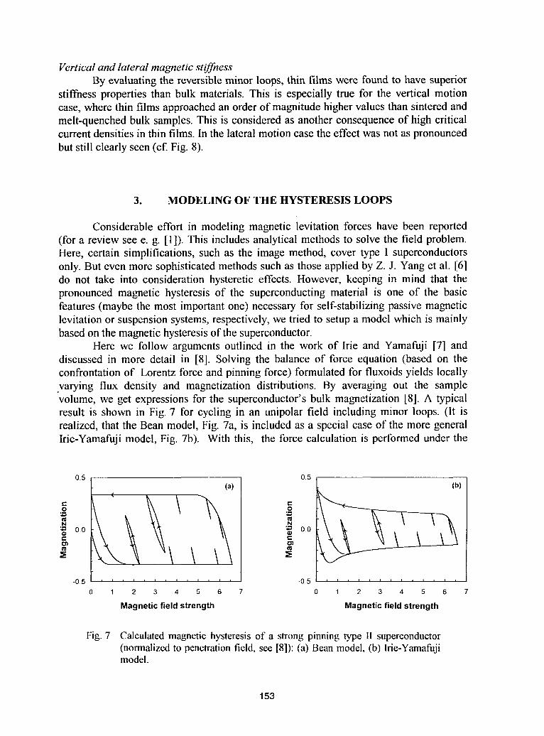
Vertical and lateral magnetic stiffnessBy evaluating the re,¢ersible minor loops, thin films were found to have superior
stiffness properties than bulk materials. This is especially true for the vertical motioncase, where thin films approached an order of magnitude higher values than sintered andmelt-quenched bulk samples. This is considered as another consequence of high criticalcurrent densities in thin films. In the lateral motion case the effect was not as pronouncedbut still clearly seen (cf. Fig. 8).
3. MODELING OF THE HYSTERESIS LOOPS
Considerable effort in modeling magnetic levitation forces have been reported(for a review see e. g. [1]). This includes analytical methods to solve the field problem.Here, certain simplifications, such as the image method, cover type I superconductorsonly. But even more sophisticated methods such as those applied by Z. J. Yang et al. [6]do not take into consideration hysteretic effects. However, keeping in mind that thepronounced magnetic hysteresis of the superconducting material is one of the basicfeatures (maybe the most important one) necessary for self-stabilizing passive magneticlevitation or suspension systems, respectively, we tried to setup a model which is mainlybased on the magnetic hysteresis of the superconductor.
Here we follow arguments outlined in the work of Irie and Yamafuji [7] anddiscussed in more detail in [8]. Solving the balance of force equation (based on theconfrontation of Lorentz force and pinning force) formulated for fluxoids yields locally.varying flux density and magnetization distributions. By averaging out the samplevolume, we get expressions for the superconductor's bulk magnetization [8]. A typicalresult is shown in Fig. 7 for cycling in an unipolar field including minor loops. (It isrealized, that the Bean model, Fig. 7a, is included as a special case of the more generalIrie-Yamafuji model, Fig. 7b). With this, the force calculation is performed under the
0.5 0.5(a) (b)
o o
N ._Ho.o '_ o.o
C t,-
-0.5 -0.5 ............
0 1 2 3 4 5 6 7 0 1 2 3 4 5 6 7
Magnetic field strength Magnetic field strength
Fig. 7 Calculated magnetic hysteresis of a strong pinning type II superconductor(normalized to penetration field, see [8]): (a) Bean model, (b) Irie-Yamafujimodel.
153
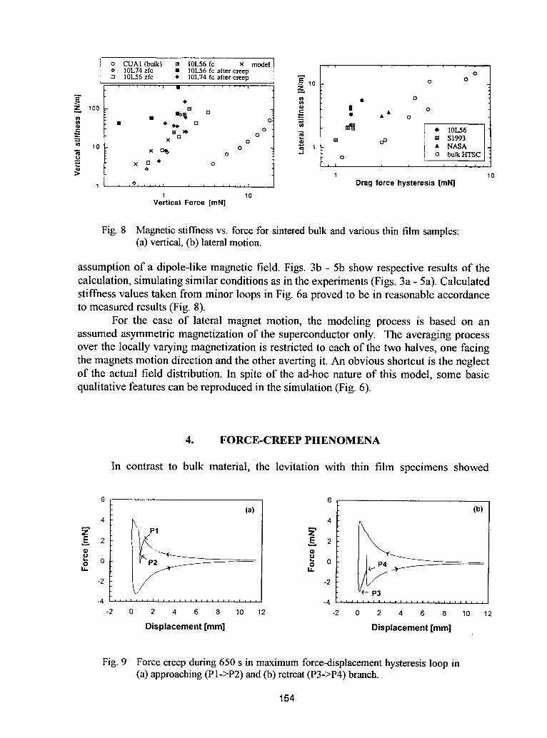
I o CUA1 (bulk) [] 10L56 fc x model , _ . .¢, 10L74 zfc • 10I..56 fc after creep o
o 10L56 zfc • 10L74 fc after creep _'_"10 o o
• II o_ I oo _m
= [] :,, o _ • 101..56'_ x r7 O .on ; S S1993o *_ [] oo :m 10 o ,_ 1 • NASA-_ x c_ o ..-=o o i o bulk HTSC_" x 0 • o
o i J L i i i i | i i
1 10
1 , ,o .... , i ........ z Drag force hysteresis [toNI1 10
Vertical Force [raN]
Fig. 8 Magnetic stiffness vs. force for sintered bulk and various thin film samples:(a) vertical, (b) lateral motion.
assumption of a dipole-like magnetic field. Figs. 3b - 5b show respective results of thecalculation, simulating similar conditions as in the experiments (Figs. 3a - 5a). Calculatedstiffness values taken from minor loops in Fig. 6a proved to be in reasonable accordanceto measured results (Fig. 8).
For the case of lateral magnet motion, the modeling process is based on anassumed asymmetric magnetization of the superconductor only. The averaging processover the locally varying magnetization is restricted to each of the two halves, one facingthe magnets motion direction and the other averting it. An obvious shortcut is the neglectof the actual field distribution. In spite of the ad-hoc nature of this model, some basicqualitative features can be reproduced in the simulation (Fig. 6).
4. FORCE-CREEP PHENOMENA
In contrast to bulk material, the levitation with thin film specimens showed
6 6(a) (b)
ZE 2 E 2
o o E 0o 0
-2 -2
_- P3
-2 0 2 4 6 8 10 12 -2 0 2 4 6 8 10 12
Displacement [ram] Displacement [mm]
Fig. 9 Force creep during 650 s in maximum force-displacement hysteresis loop in(a) approaching (P1->P2)and (b) retreat (P3->P4) branch.
154
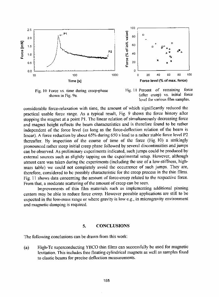
2.5 100
_._ P1 _ []
2.0 __.[. >_ 80 +
o
1.5 .=:: 60 n o_+oo_) P2 _ AXA
1,0 o_. 40 ,,. x0 _ xx
LI. _ X X0.5 o 20 xo
I,,t..
0.0 , , , , , , ,,, , , A ..... 0
10 100 1000 0 20 40 60 80 100
Time [s] Force level (% of max. force)
Fig. l0 Force vs. time during creep-phase Fig. 11 Percent of remaining forceshownin Fig.9a. (after creep) vs. initial force
level for various film samples.
considerable force-relaxation with time, the amount of which significantly reduced thepractical usable force range. As a typical result, Fig. 9 shows the force history afterstopping the magnet at a point P1. The linear relation of simultaneously decreasing forceand magnet height reflects the beam characteristics and is therefore found to be ratherindependent of the force level (as long as the force-deflection relation of the beam islinear). A force reduction by about 65% during 650 s lead to a rather stable force level P2thereafter. By inspection of the course of time of the force (Fig. 10) a strikinglypronounced rather steep initial creep phase followed by several discontinuities and jumpscan be observed. As preliminary experiments indicated, such jumps could be produced byexternal sources such as slightly tapping on the experimental setup. However, althoughutmost care was taken during the experiments (including the use of a low-stiffness, high-mass table) we could not completely avoid the occurrence of such jumps. They are,therefore, considered to be possibly characteristic for the creep process in the thin films.Fig. 11 shows data concerning the amount of force-creep related to the respective force.From that, a moderate scattering of the amount of creep can be seen.
Improvements of thin film materials such as implementing additional pinningcenters may be able to reduce force creep. However possible applications are still to beexpected in the low-mass range or where gravity is low e.g., in microgravity environmentand magnetic damping is required.
5. CONCLUSIONS
The following conclusions can be drawn from this work:
(a) High-Tc superconducting YBCO thin films can successfully be used for magneticlevitation. This includes free floating cylindrical magnets as well as samples fixedto elastic beams for precise deflection measurements.
155
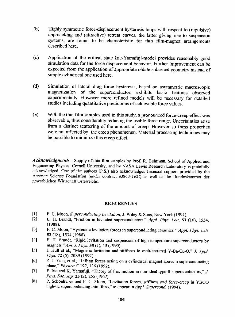
(b) Highly symmetric force-displacement hysteresis loops with respect to (repulsive)approaching and (attractive) retreat curves, the latter giving rise to suspensionsystems, are found to be characteristic for thin film-magnet arrangementsdescribed here.
(c) Application of the critical state Irie-Yamafuji-model provides reasonably goodsimulation data for the force-displacement behavior. Further improvement can beexpected from the application of appropriate oblate spherical geometry instead ofsimple cylindrical one used here.
(d) Simulation of lateral drag force hysteresis, based on asymmetric macroscopicmagnetization of the superconductor, exhibits basic features observedexperimentally. However more refined models will be necessary for detailedstudies including quantitative predictions of achievable force values.
(e) With the thin film samples used in this study, a pronounced force-creep effect wasobservable, thus considerably reducing the usable force range. Uncertainties arisefrom a distinct scattering of the amount of creep. However stiffness propertieswere not affected by the creep phenomenon. Material processing techniques maybe possible to minimize this creep effect.
Acknowledgments - Supply of thin film samples by Prof. R. Buhrman, School of Applied andEngineering Physics, Cornell University, and by NASA Lewis Research Laboratory is gratefullyacknowledged. One of the authors (P.S.) also acknowledges financial support provided by theAustrian Science Foundation (under contract #J863-TEC) as well as the Bundeskammer dergewerblichen Wirtschaft Osterreichs.
REFERENCES
[1] F.C. Moon, Superconducting Levitation, J. Wiley & Sons, New York (1994).[2] E.H. Brandt, "Friction in levitated superconductors," Appl. Phys. Lett. 53 (16), 1554,
(1988).[3] F.C. Moon, "Hysteretic levitation forces in superconducting ceramics,"Appl. Phys. Lett.
52 (18), 1534 (1988).[4] E.H. Brandt, "Rigid levitation and suspension of high-temperature superconductors by
magnets,"Am, d. Phys. 58 (1), 43 (1990).[5] J. Hull et al., "Magnetic levitation and stiffness in melt-textured Y-Ba-Cu-O," £ Appl.
Phys. 72 (5), 2089 (1992).[6] Z.J. Yang et al., "Lifting forces acting on a cylindrical magnet above a superconducting
plane," Physica C 197, 136 (1992).[7] F. Irie and K. Yamafuji, "Theory of flux motion in non-ideal type-II superconductors," d.
Phys. Soc. Jap. 23 (2), 255 (1967).[8] P. SchSnhuber and F. C. Moon, "Levitation forces, stiffness and force-creep in YBCO
high-Tosuperconducting thin films," to appear in Appl. Supercond. (1994).
156
Abstract - World Congress 1994
Hybrid superconductor magnet bearings (HSMBs) utilize hightemperature superconductors (HTSs) together with permanent magnetsto form a frictionless interface between relatively rotating parts. Theyare low mass, stable, and do not incur expenditure of energy duringnormal operation. There is no direct physical contact between rotor andstator, and hence there is no wear and tear. However, just as any otherapplications of HTSs, it requires a very cold temperature to function.Whereas this might be perceived as a disadvantage on earth, it is of nogreat concern in space or on the moon. To astronomers, the moon is anexcellent site for an observatory, but the cold and dusty vacuumenvironment on the moon precludes the use of mechanical bearings onthe telescope mounts. Furthermore, drive mechanisms with very finesteps, and hence bearings with extremely low friction are needed to trackstar from the moon, because the moon rotates very slowly. All aspectsconsidered, the HSMB is about the only candidate that fits in naturally.Here, we present a design for one such bearing, capable of supporting atelescope that weighs about 3 lbs on earth.
Author: Wei-Kan Chu
Address: Texas Center for SuperconductivityUniversity of HoustonHouston, Texas 77204-5932
Telephone: (713) 743-8250Fax: (713) 743-8201E-mail: [email protected]
157
Progress in HTS TrappedField Magnets: Jc. Area. and ApplicationsRoy Weinstein, Yanru Ren, Jianxiong Liu, Ravi Sawh_Drew Parks, Charles Foster*,Victor Obot**, G. Dickey Arndt***, and Alan Crapo****
Institute for Beam Particle Dynamics and Texas Center for Superconductivity,University of Houston, Houston, TX 77204-5506
*Indiana University Cyclotron Facility, Bloomington, IN 47405**Dept. of Mathematics, Texas Southern University, Houston, TX 77004
***Johnson Space Center, NASA, Houston, TX 77058****Emerson Electric Co., St. Louis, MO 63136
AbstractProgress in trapped field magnets is reported. Single YBCO grains with
diameters of 2 cm are made in production quantities, while 3 cm, 4 1/2 cm and 6 cmdiameters are being explored. For single grain tiles: Jc ~ 10,000 AJcm2 for melt texturedgrains; Jc - 40,000 A/cm2 for light ion irradiation; and Jc ~ 85,000 A/cm2 for heavy ionirradiation. Using 2 cm diameter tiles bombarded by light ions, we have fabricated amini-magnet which trapped 2.25 Tesla at 77K, and 5.3 Tesla at 65K. A previousgeneration of tiles, 1 cm x 1 cm, was used to trap 7.0 Tesla at 55K. Unirradiated 2.0 cmtiles were used to provide 8 magnets for an axial gap generator, in a collaborativeexperiment with Emerson Electric Co. This generator delivered 100 Watts to a resistiveload, at 2265 rpm. In this experiment activation of the TFMs was accomplished by acurrent pulse of 15 ms duration. Tiles have also been studied for application as abumper-tether system for the soft docking of spacecraft. A method for optimizing tetherforces, and mechanisms of energy dissipation are discussed. A bus bar was constructedby welding three crystals while melt-texturing, such that their a,b planes were parallel andinterleaved. The bus bar, of area - 2 cm2, carried a transport current of 1000 amps, thelimit of the testing equipment available.
I_ Introduction
Our research group has worked to develop trapped field magnets (TFM), made ofhigh temperature superconductor (HTS), since about January of 1988. We will reporthere progress on TFM since the Third World Congress on Superconductivity in MunichGermany, in 1993 (WCS III)(1). We will also report progress on certain applicationssince WCS HI. Progress prior to that date is reported in Ref. 1, and in citations therein.
Models of the persistent current flow within a TFM(2-5)show that the maximumtrappable field, Bt,max,is given approximately by
Bt,I,._x ,,_JJ(d) Eq. 1
where Jc is the critical current, d is the diameter of the contiguous current carrying region(a so-called grain, or tile), and f(d) is a complicated monotonically increasing function ofd. For example in the present range of interest (but not in general), f(d) - d1/2. A numberof analyses of trapped field magnets in the literature assume incorrect variations of Eq. 1.These lead to disagreements with data, which are then erroneously attributed to TFMproperties.
158
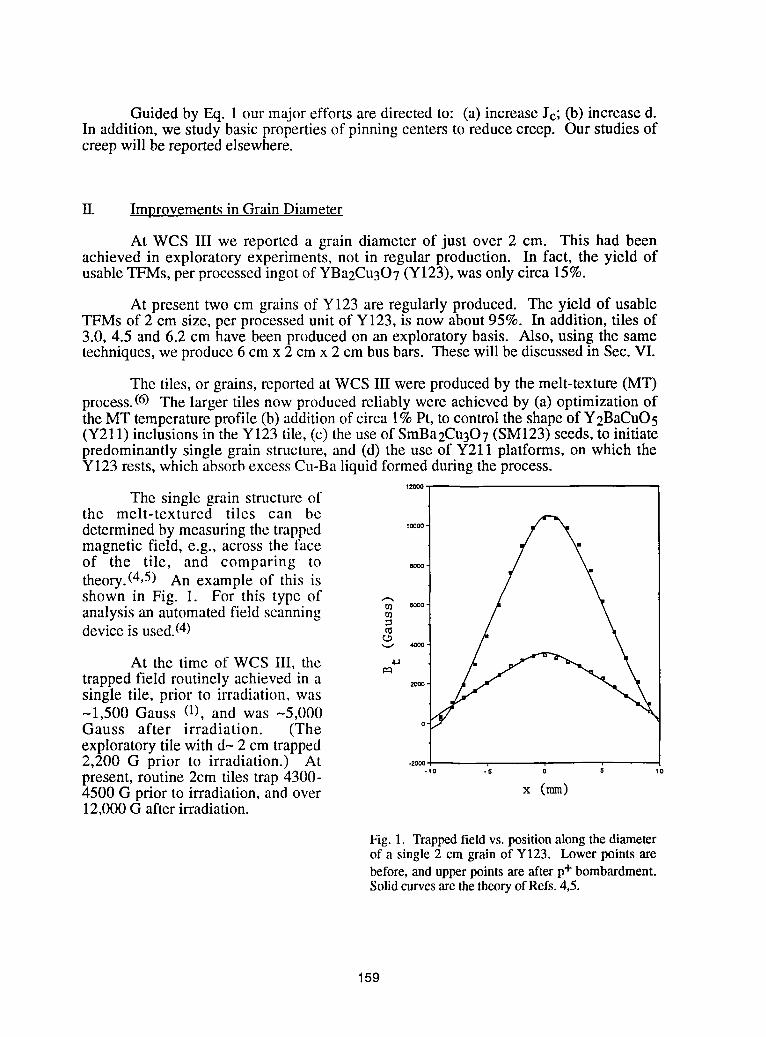
Guided by Eq. 1 our major efforts are directed to: (a) increase Jc; (b) increase d.In addition, we study basic properties of pinning centers to reduce creep. Our studies ofcreep will be reported elsewhere.
1I Improvements in Grain Diameter
At WCS III we reported a grain diameter of just over 2 cm. This had beenachieved in exploratory experiments, not in regular production. In fact, the yield ofusable TFMs, per processed ingot of YBa2Cu307 (Y123), was only circa 15%.
At present two cm grains of Y123 are regularly produced. The yield of usableTFMs of 2 cm size, per processed unit of Y123, is now about 95%. In addition, tiles of3.0, 4.5 and 6.2 cm have been produced on an exploratory basis. Also, using the sametechniques, we produce 6 cm x 2 cm x 2 cm bus bars. These will be discussed in Sec. VI.
The tiles, or grains, reported at WCS III were produced by the melt-texture (MT)process.(6) The larger tiles now produced reliably were achieved by (a) optimization ofthe MT temperature profile (b) addition of circa 1% Pt, to control the shape of Y2BaCuO5(Y211) inclusions in the Y123 tile, (c) the use of SmBa2Cu307 (SM123) seeds, to initiatepredominantly single grain structure, and (d) the use of Y211 platforms, on which theY123 rests, which absorb excess Cu-Ba liquid formed during the process.
The single grain structure ofthe melt-textured tiles can bedetermined by measuring the trapped '®_magnetic field, e.g., across the faceof the tile, and comparing to ,_theory.(4,5) An example of this isshown in Fig. 1. For this type of ,_ _.analysis an automated field scanning =device is used.(4)
At the time of WCS III, the _ '_trapped field routinely achieved in a _.single tile, prior to irradiation, was
-1,500 Gauss (l), and was -5,000 o.Gauss after irradiation. (Theexploratory tile with d- 2 cm trapped2,200 G prior to irradiation.) At .2°°°.present, routine 2cm tiles trap 4300- .,o ., 0 , 1o4500 G prior to irradiation, and over x (ram)12,000G after irradiation.
Fig. 1. Trapped field vs. position along the diameterof a single 2 cm grain of Y123. Lower points arebefore,andupperpointsareafterp+bombardment.SolidcurvesarethetheoryofRefs.4,5.
159
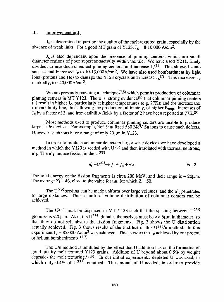
HI. Improvement in Jc
Jc is determined in part by the quality of the melt-textured grain, especially by theabsence of weak links. For a good MT grain of Y123, Jc = 8-10,000 A/cm2.
Jc is also dependent upon the presence of pinning centers, which are smalldiameter regions of poor superconductivity within the tile. We have used Y211, finelydivided, to introduce chemical pinning centers, and increase Jc(1). This showed somesuccess and increased Jc to 10-13,000A/cm2. We have also used bombardment by lightions (protons and He) to damage the Y123 crystals and increase Jc(7). This increases Jcmarkedly, to ~40,000A/cm2.
We are presently pursuing a technique(7,8)which permits production of columnarpinning centers in MT Y123. There is strong evidence(9) that columnar pinning centers(a) result in higher Jc, particularly at higher temperatures (e.g. 77K); and (b) increase theirreversibility line, thus allowing the production, ultimately, of higher Btrap. Increases ofJc by a factor of 3, and irreversibility fields by a factor of 2 have been reported at 77K.(9)
Most methods used to produce columnar pinning centers are unable to producelarge scale devices. For example, Ref. 9 utilized 580 MeV Sn ions to cause such defects.However, such ions have a range of only 20_tmin Y123.
In order to produce columnar defects in larger scale devices we have developed amethod in which the Y123 is seeded with U 235 and then irradiated with thermal neutrons,n"t- The n°t induce fission in the U235
nt +U235--) fl + f2 + n°s Eq. 2
The total energy of the fission fragments is circa 200 MeV, and their range is - 201.tm.The average Zr - 46, close to the value for tin, for which Z = 50.
The U 235 seeding can be made uniform over large volumes, and the n°t penetratesto large distances. Thus a uniform volume distribution of columnar centers can beachieved.
The U235 must be dispersed in MT Y123 such that the spacing between U235globules is <20l.tm. Also, the U235globules themselves must be << 6lam in diameter, sothat they do not self absorb the fission fragments. Fig. 2 shows the U distributionactually achieved. Fig. 3 shows results of the first test of this U235/n method. In thisexperiment Jc = 85,000 AJcm2 was achieved. This is twice the Jc achieved by our protonor helium bombardments. (1,7)
The U/n method is inhibited by the effect that U addition has on the formation ofgood quality melt-textured Y123 grains. Addition of U beyond about 0.5% by weightdegrades the melt texturing.(7, 8) In our initial experiments, depleted U was used, inwhich only 0.4% of U235 remained. The amount of U needed, in order to provide
160
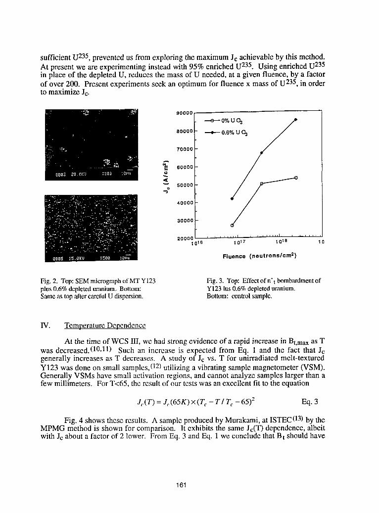
sufficient U235,prevented us from exploring the maximum Jc achievable by this method.At present we are experimenting instead with 95% enriched U235. Using enriched U235in place of the depleted U, reduces the mass of U needed, at a given fluence, by a factorof over 200. Present experiments seek an optimum for fluence x mass of U235,in orderto maximize Jc.
90000
--e--o%U_
5oooo _ 0.6%U03
70000
g..E eoooo0
"'o 50000 _-
40000
30000
20000 r _ T _1 r _ ...... I ........016 1017 1018 0
Fiuence (neutrons/cm=)
Fig. 2. Top: SEM microgmph of MT Y123 Fig. 3. Top: Effect of n°t bombardment ofplus 0.6% depleted uranium. Bottom: Y123 lus 0.6% depleted uranium.Same as top aftercareful U dispersion. Bottom: control sample.
IV. Temperature Dependence
At the time of WCS III, we had strong evidence of a rapid increase in Bt,max as Twas decreased.(10,11) Such an increase is expected from Eq. 1 and the fact that Jcgenerally increases as T decreases. A study of Jc vs. T for unirradiated melt-texturedY123 was done on small samples,(12) utilizing a vibrating sample magnetometer (VSM).Generally VSMs have small activation regions, and cannot analyze samples larger than afew millimeters. For T<65, the result of our tests was an excellent fit to the equation
J,.(T) = J,.(65K) x (Tc - T I Tc - 65)z Eq. 3
Fig. 4 shows these results. A sample produced by Murakami, at ISTEC(13) by theMPMG method is shown for comparison. It exhibits the same Jc(T) dependence, albeitwith Jc about a factor of 2 lower. From Eq. 3 and Eq. 1 we conclude that B t should have
161
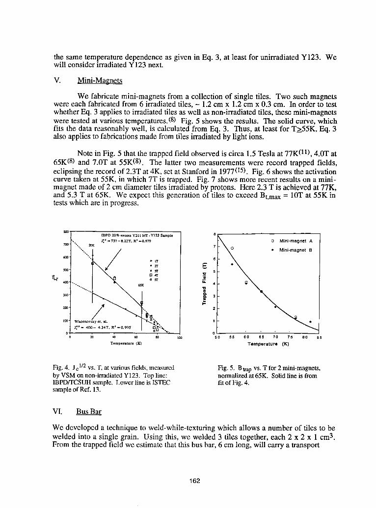
the same temperature dependence as given in Eq. 3, at least for unirradiated Y123. Wewill consider irradiated Y123 next.
V. Mini-Magnets
We fabricate mini-magnets from a collection of single tiles. Two such magnetswere each fabricated from 6 irradiated tiles, ~ 1.2 cm x 1.2 cm x 0.3 cm. In order to testwhether Eq. 3 applies to irradiated tiles as well as non-irradiated tiles, these mini-magnetswere tested at various temperatures.(8) Fig. 5 shows the results. The solid curve, whichfits the data reasonably well, is calculated from Eq. 3. Thus, at least for T>55K, Eq. 3also applies to fabrications made from tiles irradiated by light ions.
Note in Fig. 5 that the trapped field observed is circa 1.5 Tesla at 77K(11),4.0T at65K(8) and 7.0T at 55K(8). The latter two measurements were record trapped fields,eclipsing the record of 2.3T at 4K, set at Stanford in 1977(15). Fig. 6 shows the activationcurve taken at 55K, in which 7T is trapped. Fig. 7 shows more recent results on a mini-magnet made of 2 cm diameter tiles irradiated by protons. Here 2.3 T is achieved at 77K,and 5.3 T at 65K. We expect this generation of tiles to exceed Bt,max= 10T at 55K intests which are in progress.
Fig. 4. Jc 1/2vs. T, at various fiel&s,measured Fig. 5. Btrap vs. T for 2 mini-magnets,by VSM on non-irradiated Y123. Top line: normalized at 65K. Solid line is fromIBPD/TCSUH sample. Lower line is ISTEC fit of Fig. 4.sample of Ref. 13.
VI. Bus Bar
We developed a technique to weld-while-texturing which allows a number of tiles to bewelded into a single grain. Using this, we welded 3 tiles together, each 2 x 2 x 1 cm3.From the trapped field we estimate that this bus bar, 6 cm long, will carry a transport
162
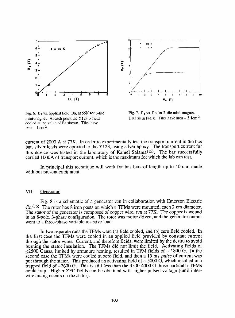
7o 65 K
6 T=55K "
5
;3 "
2
11
1 _L_ l0 L_01' 1 2 3 4 5 6 7 o 1 2 3 4 5 6 7 8 9 10
B. IT) e. (T)
Fig. 6. B t vs. applied field, Ba, at 55K for 6-tile Fig. 7. B t vs. Ba for 2-tile mini-magnet.mini-magnet. At each point the Y123 is field Data as in Fig. 6. Tiles have area ~ 3.1cm 2-cooled at the value of Ba shown. Tiles havearea- 1cm 2.
current of 2000 A at 77K. In order to experimentally test the transport current in the busbar, silver leads were epoxied to the Y123, using silver epoxy. The transport current forthis device was tested in the laboratory of Kamel Salama(15). The bar successfullycarried 1000A of transport current, which is the maximum for which the lab can test.
In principal this technique will work for bus bars of length up to 40 cm, madewith our present equipment.
VII. Generator
Fig. 8 is a schematic of a generator run in collaboration with Emerson ElectricCo.(16) The rotor has 8 iron posts on which 8 TFMs were mounted, each 2 cm diameter.The stator of the generator is composed of copper wire, run at 77K. The copper is woundin an 8-pole, 3-phase configuration. The rotor was motor driven, and the generator outputwent to a three-phase variable resistive load.
In two separate runs the TFMs were (a) field cooled, and (b) zero field cooled. Inthe first case the TFMs were cooled in an applied field provided by constant currentthrough the stator wires. Current, and therefore fields, were limited by the desire to avoidburning the stator insulation. The TFMs did not limit the field. Activating fields of<2500 Gauss, limited by armature heating, resulted in TFM fields of ~ 1800 G. In thesecond case the TFMs were cooled at zero field, and then a 15 ms pulse of current wasput through the stator. This produced an activating field of - 5000 G, which resulted in atrapped field of -2600 G. This is still less than the 3500-4000 G those particular TFMscould trap. Higher ZFC fields can be obtained with higher pulsed voltage (until inter-wire arcing occurs on the stator).
163
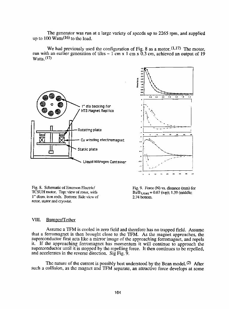
The generator was run at a large variety of speeds up to 2265 rpm, and suppliedup to 100Watts(16)to the load.
We had previously used the configuration of Fig. 8 as a motor.(1,17) The motor,run with an earlier generation of tiles - 1 cm x 1 cm x 0.3 cm, achieved an output of 19Watts.(17)
Fig. 8. Schematic of Emerson Electric/ Fig. 9. Force tiN)vs. distance (ram) forTCSUH motor. Top: view of rotor, with Ba/Bt,max= 0.67 (top); 1.39 (middle;1" diam. iron rods. Bottom: Side view of 2.74 bottom.rotor, statorand cryostat.
VIII. Bumper/Tether
Assume a TFM is cooled in zero field and therefore has no trapped field. Assumethat a ferromagnet is then brought close to the TFM. As the magnet approaches, thesuperconductor first acts like a mirror image of the approaching ferromagnet, and repelsit. If the approaching ferromagnet has momentum it will continue to approach thesuperconductor until it is stopped by the repelling force. It then continues to be repelled,and accelerates in the reverse direction. Sig Fig. 9.
The nature of the current is possibly best understood by the Bean model.(2) Aftersuch a collision, as the magnet and TFM separate, an attractive force develops at some
164
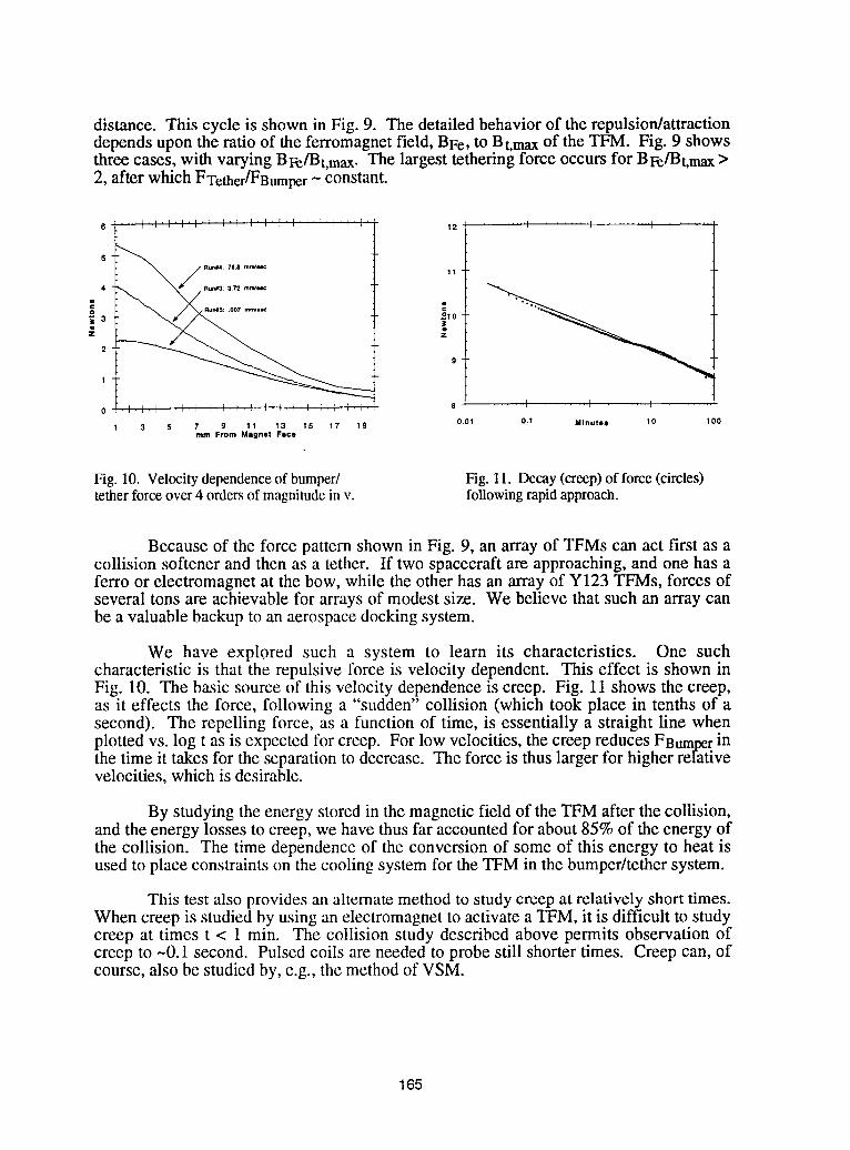
distance. This cycle is shown in Fig. 9. The detailed behavior of the repulsion/attractiondepends upon the ratio of the ferromagnet field, BFe,to Bt,maxof the TFM. Fig. 9 showsthree cases, with varying BFe/Bt,max.The largest tethering force occurs for BFe/Bt,max>2, after which FTether/FBumper~ constant.
6 12 : : J_
5
11
3 °10eZ z
2
9
I
o 8 I I ..... I
I 3 5 7 9 11 13 15 17 19 0.01 0,1 Minutes 10 100mm From Magnet Face
Fig. 10. Velocitydependenceof bumper/ Fig. 11. Decay(creep)of force(circles)tetherforceover4 ordersof magnitudein v. followingrapidapproach.
Because of the force pattern shown in Fig. 9, an array of TFMs can act first as acollision softener and then as a tether. If two spacecraft are approaching, and one has aferro or electromagnet at the bow, while the other has an array of Y123 TFMs, forces ofseveral tons are achievable for arrays of modest size. We believe that such an array canbe a valuable backup to an aerospace docking system.
We have explored such a system to learn its characteristics. One suchcharacteristic is that the repulsive force is velocity dependent. This effect is shown inFig. 10. The basic source of this velocity dependence is creep. Fig. 11 shows the creep,as it effects the force, following a "sudden" collision (which took place in tenths of asecond). The repelling force, as a function of time, is essentially a straight line whenplotted vs. log t as is expected for creep. For low velocities, the creep reduces FBumperinthe time it takes for the separation to decrease. The force is thus larger for higher relativevelocities, which is desirable.
By studying the energy stored in the magnetic field of the TFM after the collision,and the energy losses to creep, we have thus far accounted for about 85% of the energy ofthe collision. The time dependence of the conversion of some of this energy to heat isused to place constraints on the cooling system for the TFM in the bumper/tether system.
This test also provides an alternate method to study creep at relatively short times.When creep is studied by using an electromagnet to activate a TFM, it is difficult to studycreep at times t < 1 min. The collision study described above permits observation ofcreep to -0.1 second. Pulsed coils are needed to probe still shorter times. Creep can, ofcourse, also be studied by, e.g., the method of VSM.
165
This work is supported in part by grants from the Texas, through the Texas Centerfor Superconductivity at the University of Houston and the Texas Advanced TechnologyProgram, and by grants from NASA, and the Electric Power Research Institute.
References1. R. Weinstein, Invited Paper, Proc. World Congress on Superconductivity III,
Munich, pg. 1145, Pergamon Press (1992)2. C.P. Bean, Phys. Rev. Lett., 8, 250 (1962); Rev. Mod. Phys., 36, 31 (1964)3. Y.B. Kim, C.F. Hempstead, A.R. Strand, Phys. Rev., 129, 528 (1963)4. I.G. Chen, J. Liu, R. Weinstein, K. Lau, Jour. Appl. Phys., 72, 1013 (1992)5. J. Liu, I.G. Chen, R. Weinstein, J. Xu, Jour. Appl. Phys., 73, 6530 (1993)6. V. Selvamanickam, L. Gao, K. Sun, K. Salama, Appl. Phys. Lett., 54. 2352
(1989)7. R. Weinstein, et al, Invited Paper, Proc. International Workshop on
Superconductivity, Kyoto, Japan (June 1994)8. R. Weinstein, Y. Ren, J. Liu, I.G. Chen, R. Sawh, C. Foster, and V. Obot, Proc.
Int. Sympo. on Superconductivity, Hiroshima, Springer Verlag, in press (1993)9. L. Civale, A.D. Marwick, T.K. Worthington, M.A. Kirk, J.R. Thompson, L.
Krusin-Elbaum, Y. Sun, J.R. Clem, F. Holtzberg, Phys. Rev. Lett., 67, 648 (1991)10. R. Weinstein, I.G. Chen, J. Liu, and K. Lau, Jour. Appl. Phys. 70, 6501 (1991)11. R. Weinstein, I.G. Chen, J. Liu, and J. Xu, Joun. Appl. Phys., 73, 6533 (1993)12. I.G. Chen, J. Liu, Y. Ren, R. Weinstein, G. Kozlowski, and C. Oberly, Appl.
Phys. Lett., 62, 3366 (1993)13. M. Wacenovsky, R. Miletich, H. Weber and M. Murakami, Supercond. Sci.
Technol. 5, S184 (1992)14. M. Rabinowitz, H. Arrowsmith, S. Dahlgren, Appl. Phys. Lett., 30. (11), 607
(1977)15. K. Salama, ME Dept., and TCSUH, Univ of Houston, Houston, TX 7720416. R. Weinstein, A. Crapo and R.P. Sawh, contributed paper to Applied Supercond.
Conf., Boston (Oct 1994)17. C. Gillespie, Editor, Superconductor Industry, Pg. 31, Spring Issue (1993)
166
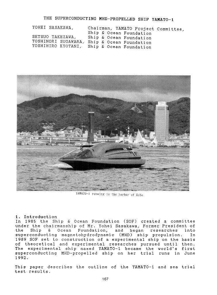
THE SUPERCONDUCTING MHD-PROPELLED SHIP YAMATO-I
YOHEI SASAKAWA, Chairman, YAMATO Project Committee,Ship & Ocean Foundation
SETSUO TAKEZAWA. Ship & Ocean FoundationYOSHINORI SUGAWARA, Ship & Ocean FoundationYOSHIHIRO KYOTANI, Ship & Ocean Foundation
YAM!T0-1runningintheharborof gobe
i. IntroductionIn 1985 the Ship & Ocean Foundation (SOF) created a committeeunder the chairmanship of Mr. Yohei Sasakawa, Former President ofthe Ship & Ocean Foundation, and began researches intosuperconducting magnetohydrodynamic (MHD) ship propulsion. In1989 SOF set to construction of a experimental ship on the basisof theoretical and experimental researches pursued until then.The experlmenhal ship named YAMATO-I became the world's firstsuperconducting MHD-propelled ship on her trial runs in June1992.
This paper describes the outline of the YAMATO-I and sea trialtest results.
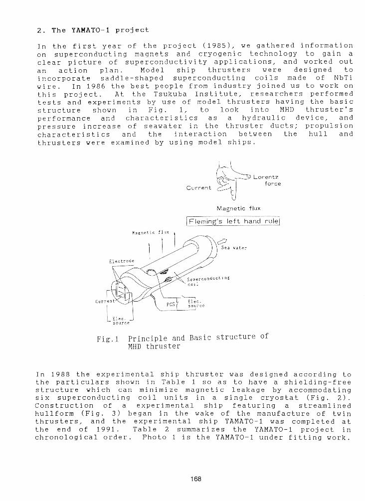
2. The YAMATO-1 project
In the first year of the project (1985), we gathered informationon superconducting magnets and cryogenic technology to gain aclear picture of superconductivity applications, and worked outan action plan. Model ship thrusters were designed toincorporate saddle-shaped superconducting coils made of NbTiwire. In 1986 the best people from industry joined us to work onthis project. At the Tsukuba Institute, researchers performedtests and experiments by use of model thrusters having the basicstructure shown in Fig. i, to look into MHD thruster'sperformance and characteristics as a hydraulic device, andpressure increase of seawater in the thruster ducts7 propulsioncharacteristics and the interaction between the hull andthrusters were examined by using model ships.
Lorentz
forceCurrent
Magnetic flux
[Fleming's left hand rule I
Magnetic flux
Sea water
Electrode
Superconductin{coil
Current Elec.
SourceElec.source
Fig.l Principle and Basic structure ofMHDthruster
In 1988 the experimental ship thruster was designed according tothe particulars shown in Table 1 so as to have a shielding-freestructure which can minimize magnetic leakage by accommodatingsix superconducting coil units in a single cryostat (Fig. 2).Construction of a experimental ship featuring a streamlinedhullform (Fig. 3) began in the wake of the manufacture of twinthrusters, and the experimental ship YAMATO-I was completed atthe end of 1991. Table 2 summarizes the YAMATO-I project inchronological order. Photo 1 is the YAMATO-I under fitting work.
168
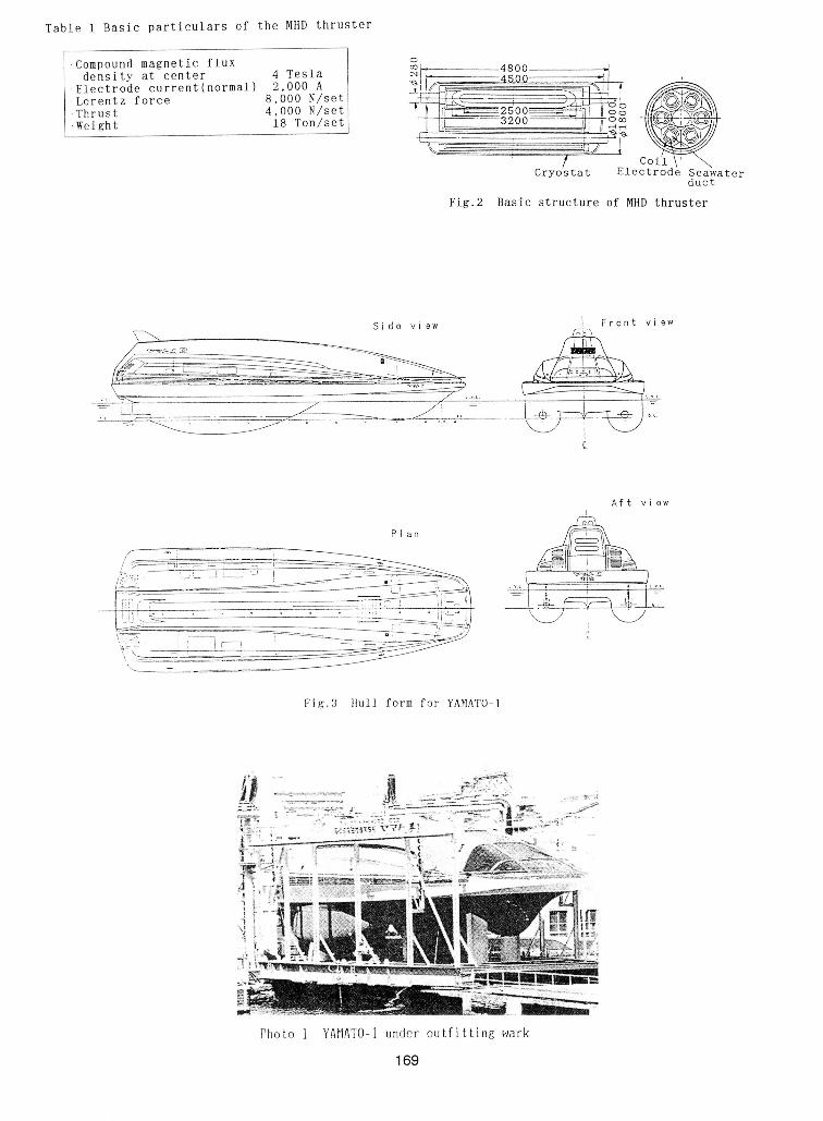
Table 1 Basic particulars of the MHD thruster
•Compound magnetic flux _J 4800 ,1
density at center 4 Tesla _!t'_ 4500 _ ,•Electrode current(normal) 2,000 A _t_F_ / _---_----_T_,
•Thrust 4,000 N/set _r_25_00
•Weight 18 Ton/set _'--3200__. . . __j.__ _
_.--A' "----'--_" _
!Cryostat Electrode Seawater
duct
Fig.2 Basic structure of _HD thruster
Side view Front view
Aft viewI
Fig.3 tlull form for YANATO-1
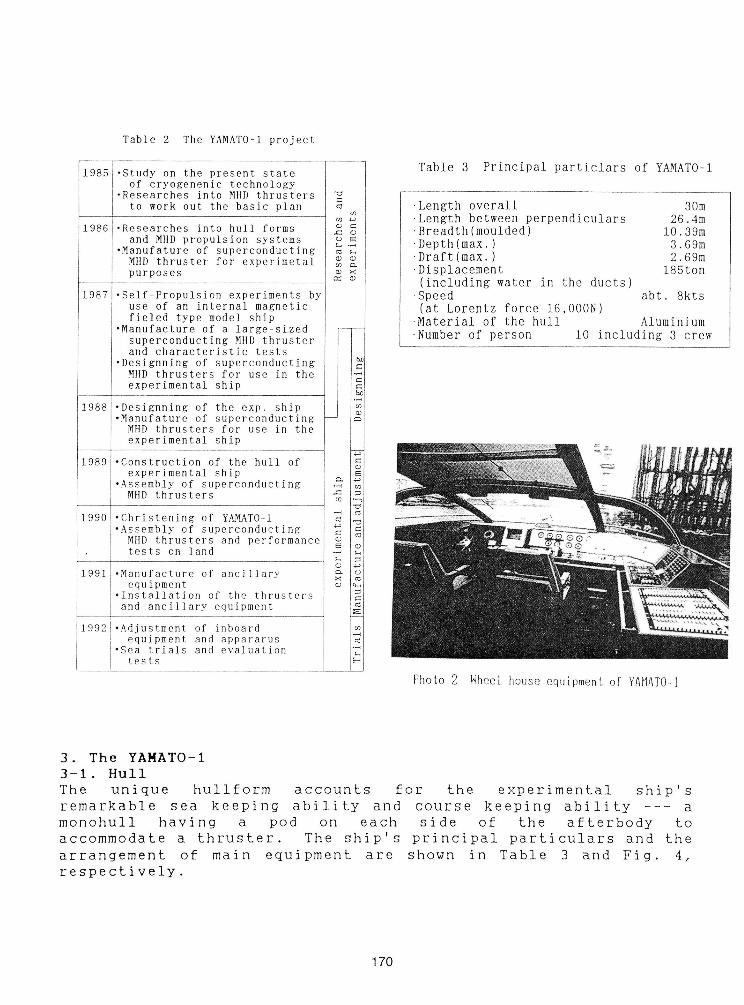
Table 2 The YAMATO-1 project
Table 3 Principal particlars of YAiYb_TO-I1985 -Study on the present stateof cryogenenic technology
-Researches into MHD thrustersto work out the basic plan _ Length overall 30m
_ Length between perpendiculars 26.4m1986 -Researches into hull forms ¢ g Breadth(moulded) i0.39m
and MHD propulsion systems _ E•_ Depth(max.) 3 69m• Manufature of superconducting _ _MHD thruster for experimetal _ _ Draft(max.) 2.69m
Displacement 185tonpurposes _ _ (including water in the ducts)
1987 -Self-Propulsion experiments by Speed abt. 8ktsuse of an internal magnetic (at Lorentz force 16,00ON)fieled type model ship Material of the hull Aluminium
•Manufacture of a large-sized ---- Number of person i0 including 3 crewsuperconducting MHD thrusterand characteristic tests
•Designning of superconductingMHD thrusters for use in theexperimental ship
1988 .Designning of the exp. ship m• Manufature of superconducting --
MHD thrusters for use in theexperimental ship
1989 .Construction of the hull ofexperimental ship
• Assembly of superconducting ._MHD thrusters _ =
1990 .Christening of YANATO1 _ _• Assembly of superconducting _ =
MHD thrusters and performance _ _ a_tests on land
1991 .Manufacture of ancillary oequipment _ _
• Installation of the thrusters =and ancillarv equipment
1992 -AdJustment of inboardequipment and appararus
• Sea trials and evaluationtests
Photo 2 _heel house equipment of Y_MATO1
3. The YAMATO-I3-i. HullThe unique hullform accounts for the experimental ship'sremarkable sea keeping ability and course keeping ability amonohull having a pod on each side of the afterbody toaccommodate a thruster. The ship's principal particulars and thearrangement of main equipment are shown in Table 3 and Fig. 4,respectively.
170
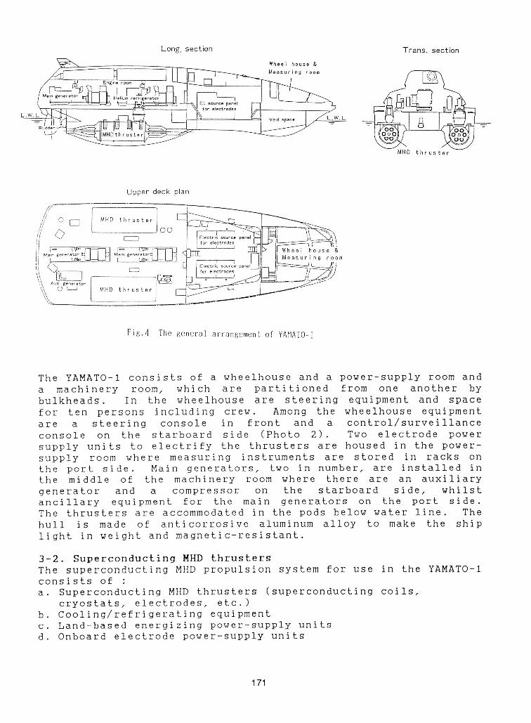
Long. section Trans. section
Wheel house &
Engune room
I
t_.w. [ ..W.L _
_[ _.=.
L t./ MHOthrust
MHD thruster
Upper deck plan
![re_ [.i.,....;._ _ I'_hee]'h'ouse',,,Measuring r::rn
Fig.4 The general arrangement of YAH_TO-1
The YAMATO-I consists of a wheelhouse and a power-supply room anda machinery room, which are partitioned from one another bybulkheads. In the wheelhouse are steering equipment and spacefor ten persons including crew. Among the wheelhouse equipmentare a sheering console in front and a control/surveillanceconsole on the starboard side (Photo 2). Two electrode power
supply units to electrify the thrusters are housed in the power-supply room where measuring instruments are stored in racks onthe port side. Main generators, two in number, are installed inthe middle of the machinery room where there are an auxiliarygenerator and a compressor on the starboard side, whilstancillary equipment for the main generators on the port side.The thrusters are accommodated in the pods be!ow water line. Thehull is made of anticorrosive aluminum alloy to make the shiplight in weight and magnetic-resistant.
3-2. Superconducting MHD thrustersThe superconducting MHD propulsion system for use in the YAMATO-Iconsists of :a. Superconducting MHD thrusters (superconducting coils,
cryostats, electrodes, etc.)b. Cooling/refrigerating equipmentc. Land-based energizing power-supply units
d. Onboard electrode power-supply units
171
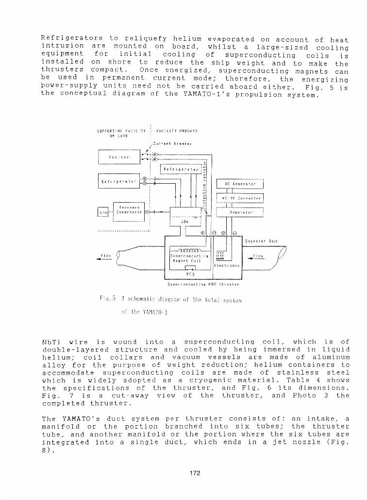
Refrigerators to reliquefy helium evaporated on account of heat
intrusion are mounted on board, whilst a large-sized cooling
equipment for initial cooling of superconducting coils isinstalled on shore to reduce the ship weight and to make thethrusters compact. Once energized, superconducting magnets canbe used in permanent current mode; therefore, the energizingpower-supply units need not be carried aboard either. Fig. 5 isthe conceptual diagram of the YAMATO-I's propulsion system.
SUPPORTING FACILITY FACILITY ONBOARDON LAND
Ourrent breaker
Refrigerater
I Re[r iKerat°r _--_# l I [ kC 0..... tor I
illl" ,AC'DC Converter
. . .
pcs
Superconducting MHD thruster
Fig.5 A schematic diagram of the total system
of the YAHATO-I
NbTi wire is wound into a superconducting coil, which is of
double-layered structure and cooled by being immersed in liquid
helium; coil collars and vacuum vessels are made of aluminumalloy for the purpose of weight reduction; helium containers toaccommodate superconducting coils are made of stainless steelwhich is widely adopted as a cryogenic material. Table 4 showsthe specifications of the thruster, and Fig. 6 its dimensions.Fig. 7 is a cut-away view of the thruster, and Photo 3 thecompleted thruster.
The YAMATO's duct system per thruster consists of: an intake, amanifold or the portion branched into six tubes; the thrustertube, and another manifold or the portion where the six tubes areintegrated into a single duct, which ends in a jet nozzle (Fig.8).
172
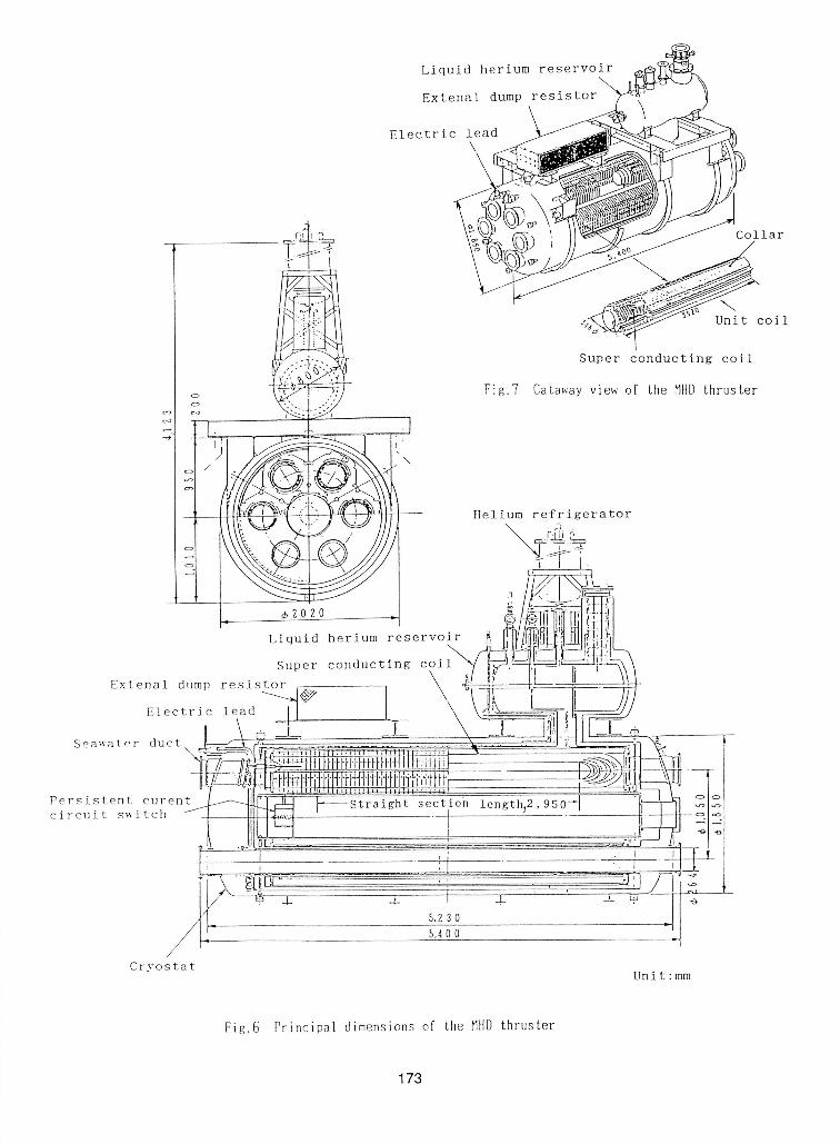
Liquid herium reservoir
Extenal dump resistor
Electric lead\
\
Ilelium refrigerator
¢2020
Liquid herium reservoir
Super conducting coil
Extenal dump
resistor__r 1E]ectrJc
lead___i - _J_Seawater duct
Persistent curent ight sectioh length_2,950-J
circuit switch [
i ; I t
5,2305,400
Cryostat Unit :ram
Fig.6 PrincipaI dimensions of the MIlDthruster
173
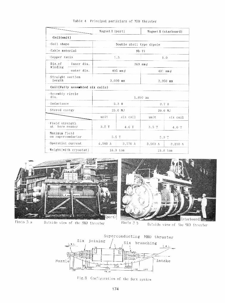
Table 4 Principal particlars of MHDthruster
Magnet ! (port) _lagnetl (starboard)
Coil(unit)
-Coil shape Doub]e shell type dipole
•Cable material Nb.Ti
-Copper ratio 1.3 1.0
•Dia.of inner dia. 360 mm¢winding
outer dia. 405 mm_ 401 mm¢
•Straight sectionlength 3,000 mm 2,950 mm
Coil(Fully asselbled six eoils)
.Assembly circledis. 1,050 mm
IInductance 3.3 H 3.7 It
Stored energy. 23.0 MJ 20.0 MJ
j unit six coil unit six coil|
-Field strength [at bore center 3.5 T 4.0 T 3.5 T 4.0 T
.Maximum fieldon superconductor 5.5 T 5.9 T
4,580 A 3,770 A 3,960 k i 3,210 A" Ope_tlon currentT
.Weight(with cryostat) _ 18.0 ton 15.8 ton1
(starboard
Photo 3 a Outside vie_ of the NtD thruster Photo 3 b Outside vie_+of the _IlIDthruster
Superconducting MHD thruster1
[wk Six joining / Six branching--' " " ' _ ' ' t_.k.
+zz. • 0 7't 7'0 2700 400
Fig.8 Configuration of the duct system
174
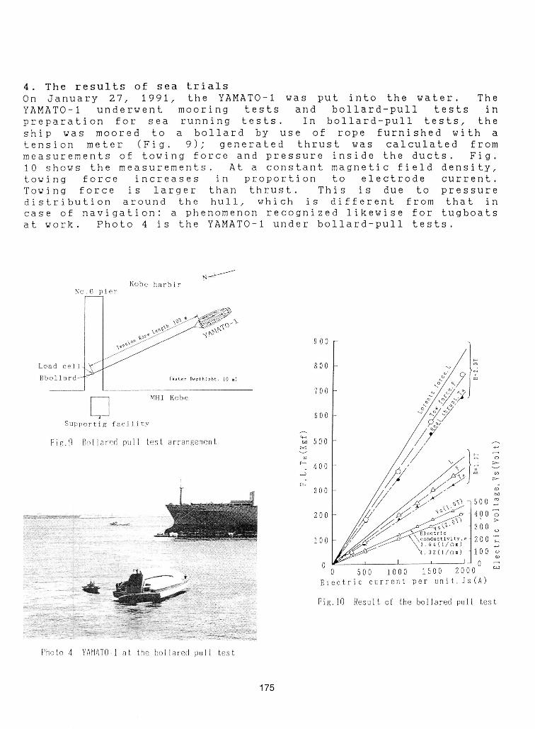
4. The results of sea trialsOn January 27, 1991, the YAMATO-I was put into the water. TheYAMATO-I underwent mooring tests and bollard-pull tests inpreparation for sea running tests. In bollard-pull tests, theship was moored to a bollard by use of rope furnished with atension meter (Fig. 9)j generated thrust was calculated frommeasurements of towing force and pressure inside the ducts. Fig.i0 shows the measurements. At a constant magnetic field density,towing force increases in proportion to electrode current.Towing force is larger than thrust. This is due to pressuredistribution around the hull, which is different from that incase of navigation: a phenomenon recognized likewise for tugboatsat work. Photo 4 is the YAMATO-I under bollard-pull tests.
Kobe harbirNo 6 pzer
be %__
Load cell.\_j'JJ 800 o
Bbollard_-_" (_.t,r Deptb:_bt. i0 m) =
700
NHI Kobe. 600Supportig facility
o_
Fig.9 Bo] ared pull test arrangement _ 500 .-.
0
400
M 300 JbO500 '_
_,___ .... 200 400o:-:.,-_,- • . ,_ 300
.- Electric o
" - - - , i00 ,eo_duotlvlty._2003.64(I/Qm)
. . 32(I/o_) - 100 oo
: " .... I ]• 0 0 ._
- - 0 500 1000 1500 2000Electric current per unit, Js(A)
• Fig. 10 Result of the bollared pull test.£. °
Photo 4 Y_1td!_TO-1at the bollared pull test
175
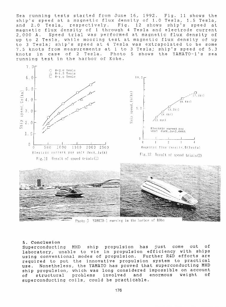
Sea running tests started from June 16, 1992. Fig. ii shows theship's speed at a magnetic flux density of 1.0 Tesla, 1.5 Tesla,and 2.0 Tesla, respectively. Fig. 12 shows ship's speed atmagnetic flux density of 1 through 4 Tesla and electrode current2,000 A. Speed trial was performed at magnetic flux density ofup to 2 Tesla, while mooring test at magnetic flux density of upto 3 Tesla; ship's speed at 4 Tesla was extrapolated to be some7.5 knots from measurements at 1 to 3 Tesla; ship's speed of 5.3knots in case of 2 Tesla. Photo 5 shows the YAMATO-I's searunn ng test in the harbor of Kobe.
?0-B=2.0 Tesla
z_ B=l.5 Tesla
6 0 - _ B=l.O Tesla I0.0 --
5 0-
-_ _< -" (7 5kt)
v v .6kt)
c_ i /(4. 6kt)U9 C_ /
"-- /(3. 6kt)
_2.0_'_ Electric curent per
i . 0 - /" unit duct,Js-_2,0OOA
0 I i [ J
0 i I i i i i 2 3 4500 ]000 !500 2000 2500 h{agnetic flux density. B(TesIa)
Electric current per unit duct,Js(k) Fig.]2 [_esult of speed trials(2)Fig.!] Result of speed trials(l)
Photo 5 YAHATO-1running in the harbor of KObe
5. ConclusionSuperconducting MHD ship propulsion has just come out oflaboratory, unable to vie in propulsion efficiency with shipsusing conventional modes of propulsion. Further R&D efforts arerequired to put the innovative propulsion system to practicaluse. Nonetheless, the YAMATO has proved that superconducting MHDship propulsion, which was long considered impossible on accountof structural problems involved and enormous weight ofsuperconducting coils, could be practicable.
176

THIS PAGE INTENTIONALLY LEFT BLANK


PerformanceCharacterization
Session I Chair: Dr. R. K. PandeyCo-Chair: Dr. U. Varshney
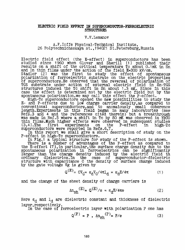
ELECTRICFIELDEFFECTIN SUPERCONDUCTOR-FERROELECTRI0STRUCTURES
V.V.Lemanov
A.F.IoffePhyslcal-TechnicalInstitute,26 Polytechnlcheskayast.,194021St.Petersburg,Russla
Electric field effect (the E-effect)in superconductorshas beenstudied since 1960 when Glover and Sherlll [I] published theirresultson a shiftof the criticaltemperatureTc about 0.1inKin Snand In thin filmsunder the actionof the fieldE=300kV/cm.Stadler [2] was the first to study the effect of spontaneouspolarizationof ferroelectrlcsubstrateon the electricpropertiesof superconductors.Heobservedthat the reversalof polarizationofTGS substrateunder action of external electric field in Sn-TGSstructuresinduced the Tc shift in Sn about 1.3 inK.Since in thiscase the effectis determinednot by the electricfield but by thespontaneouspolarlzatlon,wemay call this effectthe P-effect.
High-Tcsuperconductorsopenedthe new possibilitiesto studytheE- and P-effectsdue to low charge carrierdenslty,ascomparedtoconventional superconductors,andto anomalously small coherencelength.Experimentsin this field began in many laboratories(seeRefs.3and 4 and the referencescited therein)but a breakthroughwas made in Ref.5where a shiftin Tc by GO mE was observedin YBCOthin films.Muchhigher effectswere observedin subsequentstudies[3,4].The first experiments on the P-effect in hlgh-Tcsuperconductorswere reportedin Refs.6,7.
In this reportwe shallgive a shortdescriptionof studyon theP-effectin hlgh-Tcsuperconductors.
In Fig.1a typicalstructurefor studyof the P-effectis shown.There is a number of advantagesof the P-effectas comparedto
the E-effect[7],in particular,the surfacechargedensitydue to thespontaneouspolarizationin ferroelectrlcscan be significantlylarger than the charge density induced by the electric fieldordinary dielectrlcs.In the case of superconductor-dielectrl_structurewith capacitanceC the densityof surface chargeinducedby the gate voltageVg is givenby
Q(E)=CVG= SdVG/4E1d = SdE/4% (I)
and the changeof the sheetdensityof chargecarriersis
Ansh(E)=Q(E)/e= SdE/4xe (2)
Here sd and id are dielectricconstantand thicknessof dielectriclayer,respectlvely.
In the case of ferroelectrlclayerwith polarizationP one has
Q(P) = P , _Ansh(P)=P/e (3)
180
OnecanrewriteEqs.2and3 in themoreconvenientform
Ansh(E)=5.5 105SdE (2a)Ansh(P)=6.2 1018P (3a)
.% --2 •whereAnshIs In ,Jm ,Eis in V/cmandP Is in C/cm2For the ratio of carrierssheet densitycange in the P- and
E-effectswe have
Ansh(P)/Ansh(E)= 4_P/SdE= 1.11013(P/sdE) (4)
If we take the spontaneouspolarizationfop ferroelectrlcperovsklteP= 10-4 C/cm2 ( which seems to be the maximumexperimentallyobservedvalue)and supposethatdielectriclayerhasdielectricconstantSd = 100,thentheE-effectwlllbe equalto theP-effectonlyin the electricfieldE = I.I 107 V/cm.ThlsvalueIsfarbeyondthebreakdownfieldvaluesfordielectriclayers.
The othercharacterlstlc,veryimportantin thestudyof theE-andP-effects,lsthe Thomas-Fermlscreeninglengthwhichdescribesthescreeningof theelectric fieldor polarl_atlonby chargecarriersinmetalsor degeneratesemiconductors.ThescreeninglengthIs givenby
IT.F.=(SEF/6_ne2 )I/2 (5)or
IT.F.=6.1 102 (SEF/n)I/2 (5a)
where_ Is the dielectricconstantof a superconductor,EF Is theFermienergy,andn Is the volumecarrierdensity.InEq.GaIT.F.is
in cm,EF Is in eV,andn is in cm-3.For YBCOusingEq.5aand the appropriatevaluesof parameterswehaveas an upperlimitIT.F.= I nm.The changeof sheetdensityin a superconductorunderactionofelectricfieldorpolarizationis distributedalongthlslengthandfor the totalrelativechangeof volumecarrierdensityin thesuperconductorthinfllmof thicknessIT.F.we have
An/n= Ansh/iT.F.n (6)
For the fllmthicknessis largerthanIT.F.the changeof sheetdensityshouldbe referredto the thicknessis.If the fllmresistanceIs completelydeterminedby thecarrierdensitythenoneobtains
AR/R= _nsh/lsn (7)
181
21 -3 -5 2If we take is= 100 nm, n= 4 10 cm and P= 7 10 C/cm
then we have AR/R= 10-2 ,that is the switching of polarization In aferroelectric from +P to -P should give the chaflgein resistancein an adjacent superconductor fllm about 2_ .If the criticaltemperature Tc of the superconductor is also proportional to thecarrier denslty,then one should observe the Tc shift also by 2% .
The change of charge carrier density should also influence the
resistance of superconductor in the mixed state though the mechanismof this effect may be different as compared to the normal state.
In Fig.2a the resistance change in the mixed state of YBCO filmwlth thickness is 200 nm is shown as a function of electricfield applied to BaTI03 substrate.Flg.2b shows the polarizationhysteresis loop in the same substrate at the same temperature.TheYBCO film is deposited on (001)plane of BaTlO3,the thickness of thesu.bstrateis about 0.5 ram.FromFlg.2 It follows that there Is aals_lncz _orre_ation between the resistance and polarizationchanges. The Tc shift in the same structure determined fromtemperature dependence of resistance is 0.5 K or 0.5 _ whichis near to the estimation from Eq.7.
In Flg.3 the resistance temperature dependences of YBCO filmsdeposited on LiNbO_ substrate are shown.The spontaneous polarization
-5 _-of LiNbO3 is 7 10 C/cm , however the polarization in thiscrystal cannot be reversed at low temperatures due to very hlghcoercive field.Therefore to observe the P-effect YBCO films weredeposited on the opposite sides ( +P and -P) of two single-domainLiNb03 plates In one experiment in the identical conditions.One cansee that there is a considerable shift of the Tc at R =0 by about40 K.Thls shift is much larger than predicted by Eq.7 for the fllmwith thickness about IO0 nm.
For the possible application It is important to study theP-effect in superconductor-ferroelectrlclayered structure whereboth superconductorand ferroelectrlcare deposited as thin films.Anexample of such a structure is shown in Flg.4 [8].YBCO film 400 nmthick is deposited on NdGa03 by laser ablation method.Onto the YBCOfllm BaSrTI03 film wlth thickness 1500 nm Is deposited by rfmagnetron sputtering technlque.UslngBaSrTI03 solid solutions givesthe possibility to change t_ieferroelectrlc Curie temperature whichcan vary from liquid Helium region up to 400 K.Thls possibility maybe useful to optimize the conditions for the E- and P-effects.Somecharacteristicsof YBCO-BST structure are presented in Flg.5.
Along wlth the true E- and P-effects the elastic strain effect(the S-effect) should also exlst.Indeed,underthe action of electricfield we have electrostrlctlve (any solids) and piezoelectric(crystals without inversion symmetry) strains in dielectric(ferroelectrlc) layers and there will be consequently elasticstrains in superconductor film.These strains can change thesuperconductorelectric propertles.Itwas shown [9] that the elasticstrains in BaSrTI03 ceramic substrates resulted in the shift of thesuperconductor critical temperature Tc by 0.03 K in the electricfield about I0 kV/cm.
The experimental results on the P-effect presented in Flgs.2 and
182
3 have been obtained for YBCO films with thickness about 100 nm thatis much larger than the Thomas-Fermi screening length.To increasethe P-effect it is necessary to use ultrathin YBOO films comparableto the Thomas-Fermi screening length [lO].Let us estimate thevalue of polarization of a ferroelectrlc layer which could switchultrathin YBCO film from the N-state to the S-state,and viceversa,due to the P-effect.We shall discuss three-layered structureshown in Flg.6. Using Eqs.3 and 7 and assuming that All/R=I we have
0
P (C/cm") = (lsni6.2) 10-18 ,whereis is in cm andn is in cm-3.Then for is=2.5 nm and n = 5 I021cm-3 one obtains P=2 10-4C/cm2.This value sould be divided over 4 due to the P reversal from +P to-P and due to the double ferroelectrlc layers in Flg.6. So, finallywe have P= 5 10-5 2C/cm ,more or less ordinary value for a number of''strong'' ferroelectrlc crystals.
Another approach to this problem may also be used.If we assumethat the resistance of t_e ultrathin film is of the order of thequantum unit R = h/4e = 6 45 k_ [11],and the change of theqresistance under action of polarlzatlon,for transition from theN-state to the S-state,has the same value,then we obtain P = I/_R_=
'_ -4 2 H=4e2/_h or P (C/cm_) =I .55 10 /_ ,where _ is mobility in cm /V s.For the mobility of the order of I cm2/V s the polarlzatlon Phas the same value as in the first estimation.
Thus,for ultrathin superconductor film it is possible to switchthe film from the N-state to S-state by switching the polarizationin ferroelectrlclayers under action of the electric field (Flg.6).
It should be noted that ferroelectrlc layers insuperconductor-ferroelectrlc structures may have ferroelectrlcdomain structure which can be used to form some weak links and N-SJunctions in adjacent superconductorlayers [12].
The P-effect in superconductors,aswell as the E-effect,can inprinciple find many technical applications [4] :superconducting_leld effect transistors (SuFET),electrocryotrons,mlxers,adJustablefilters,etc.Theadvantage of the P-effect is the possibility to havedevices with long-term memory.
183
REFERENCES
I.R.E.GloverandM.D.Sherill,Phys.Rev.Lett.5,248,1960.2.H.L.Stadler,Phys.Rev.Lett.14,979,1965.3.J.Mannhart,Mod.Phys.Lett.B6,555,1992.4.V.V.LemanovandA.L.Kholkln,Fiz.Tverd.Tela36,1537,1994.5.J.Mannhart,D.G.Schlom,J.G.Bednorz,andK.A.M{ilIer,Phys.Rev.Lett.67,2099,1991.
6.V.V.Lemanov,A.L.Kholkln,andA.B.Sherman,JETPLett.56,562,1992.7.V.V.Lemanov,A.L.Kholkin,andA.B.Sherman,Supercond.Sci.Technol.6,814,1993.
8.B.M.Goltsman,V.V.Lemanov,A.L.Kholkln,andS.O.Shulman,Tech.Phys.Lett.19,639,1993.
9.V.V.Lemanov,V.V.Makarov,andA.B.Sherman,Fiz.Tverd.Tela36,NS,1994.IO.X.X.Xl,C.Doughty,A.Walkenhorst,C.Kwon,Q.LI,andT.Venkatesan,
Phys.Rev.Lett.68,1240,1992.11.D.B.Havlland,Y.Llu,andA.M.Goldman,Phys.Rev.Lett.62,2180,1989.12.V.V.Lemanov,Tech.Phys.Lett.19,714,1993.
184
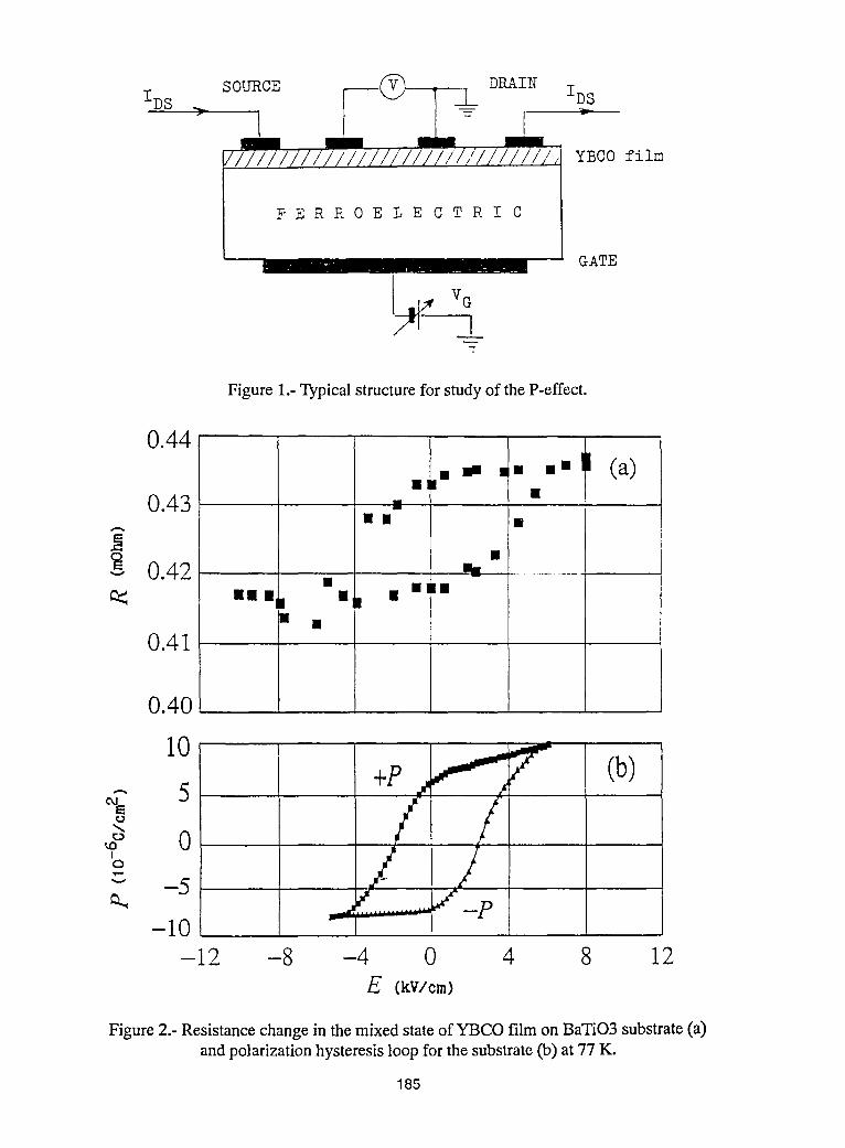
sou_c_ __CV__.__IXDRAIN
//////////////////////////////_ Y_COr±_
FERROELECTRIC
GATE
1 vo-f
Figure 1.-Typical structure for study of the P-effect.
0.44• m ,- ," (a)
Ili
0.43 -"ill IN
--_ 0.42 "• Ill
atomnmlu II a •lm []
0.41
0.40
10 , 7" (b)
_' 0
_ -5-10
- 12 -8 -4 0 4 8 12E CkV/cm)
Figure 2.- Resistance change in the mixed state of YBCO film on BaTiO3substrate (a)and polarization hysteresis loop for the substrate (b) at 77 K.
1135
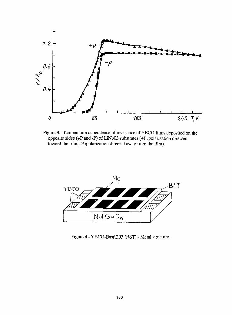
F1.2 +p ,A..__
0 8o _0 2_,0T,K
Figure 3.- Temperaturedependence of resistance ofYBCO films deposited on theopposite sides (+P and -P) of LiNb03 substrates (+P :polarizationdirectedtoward the film, -P :polarizationdirectedaway from the film).
Nd GoO_
Figure 4.- YBCO-BasrTi03 (BST) - Metal structure.
186
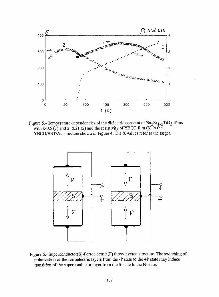
_ m__.cm400 4
-'kZ_ ..'" Q
1O0 1
0 z ,J , i t , 00 50 1O0 150 200 250 300
T (K)
Figure 5.- Temperature dependenciesof the dielectric constantof BaxSrl_xTiO3filmswith x-0.5 (1) and x=0.21 (2) and the resistivityof YBCO film (3) in theYBCO/BST/Au structure shown in Figure 4. The X values refer to the target.
IF' .---o _F ---o- -!-
_ _---,,---o _ _--' ,-----o+
IrT
Figure 6.- Superconductor(S)-Ferroelectric(F) three-layered structure.The switchingofpolarization of the ferroelectric layers from the -P state to the +P state may inducetransition of the superconductorlayer from the S-state to the N-state.
187
OXIDE PEROVSKITE CRYSTALS FOR HTSC FILM SUBSTRATESMICROWAVE APPLICATIONS
A.S. BHALLA AND RUYAN GUO
Materials Research Laboratory, The Pennsylvania State UniversityUniversity Park, PA 16802
ABSTRACT
The research focused upon generating new substrate materials for the deposkion ofsuperconducting yttrium barium cuprate (YBCO) has yielded several new hosts incomplex perovskites, modified perovskites, and other structure families. New substratecandidates such as Sr(Alv2Tav:)O3 and Sr(All/:Nbl/2)O3,Ba(Mgv3Ta:/3)O3 in complexoxide perovskite structure family and their solid solutions with ternary perovskite LaA103and NdGaO3 are reported. Conventional ceramic processing techniques were used tofabricate dense ceramic samples. A laser heated molten zone growth system was utilizedfor the test-growth of these candidate materials in single crystal fiber form to determinecrystallographic structure, melting point, thermal, and dielectric properties as well as tomake positive identification of twin free systems. Some of those candidate materialspresent an excellent combination of properties suitable for microwave HTSC substrateapplications.
INTRODUCTION
There is great interest worldwide in the deposition of high quality thin films of high Tcsuperconductors (HTSC), using a whole variety of available deposition techniques. Theselection of useful substrate materials is of first importance and is subjected to a numberof constrains such as: thermal and chemical stability under the conditions used in the filmprocessing and operating; suitable lattice parameter and ionic structure matching; thermalcompatibility in terms of thermal expansion matching over the temperature range of filmprocessing and operating; physical properties suitable for specific use (for instance thedielectric constant and loss for electronic devices and high thermal conductivity for high-power-density applications); commercial availability and if possible, low cost.
In addition to satisfy the general requirements, substrates to be used in microwavedevices must be twin-free single crystals with potential to be grown in large size (2-4"wafer). Congruent melting compositions with modest melting temperatures are thereforefavorable. The dielectric constant influences the propagation speed and the packagedimensions therefore a moderately low dielectric constant (<25) is required. Because theconductor loss of the superconductor is diminished, the role of the dielectric loss becomescriticallyimportant. Very low dielectricloss (< 10-4)is therefore demanded.
The potential application of YBCO superconductor to the development of ultra highdensity interconnect systems for a new generation of high speed high density multichip
188
A. S. Bhalla and Ruyan Guo
modules dictates new requirements for the substrate design. An essential feature is thegeometry of the X and Y layers of HTSC lines that must have geometries in cross sectionof order 2 x 1 _t meters thus necessitating a current carrying capability for the HTSC of_106 A/cm2. For this current capability clearly the YBCO must be highly grain orientedvery near to single crystal, so that the whole multilayer structure is in the form of highlyoriented overgrowths on a single crystal substrate. Impedance characteristics for theinterconnect structure dictate that the dielectricsused must be of low permittivity (ideally<10) if the geometry is to be preserved. Highly oriented thin films (2 _tmor above) willbe needed for the separation of strip lines and ground plane structures. Dielectric lossrequirements are a little less stringent than those required for the microwave applications;however, tank < 0.001 is highly desirable at the 77K working temperature.
A family of substrates with the perovskite structure is most important as thosematerials are among the most obvious candidates for epitaxial growth of YBCO films.Substrates of perovskite structure usually have the ideal cubic (such as SrTiO3), doublecell cubic (such as Ba2YSbOr), hexagonal distorted pseudo cubic (such as LaA103) orother pseudo cubic cells (such as NdGaO3 that has the [GdFeO3] structure withorthorhombic symmetry). SrTiO3 crystals of high quality and large sizes, though arereadily available and yield the best epitaxial quality thin films (primarily due to their closeinteratomic structure matching to the HTSC), have high dielectricconstant (>300) arisingfrom the phase transition near the working temperature (-110K). Another probably themost used substrate currently, LaAIO3,though good in lattice matching and of reasonabledielectricproperties, is heavily twinned and goes through a ferroelastic phase transition at-435°C. t These macroscopic defects in the crystals are not tolerable in substrates usedfor complex microcircuits.
In our ongoing search for substrates suitable for microwave device and integratedcircuit applications, the focus has been upon developing and identifying new substratematerials primarily with perovskite structures for the deposition of superconductingyttriumbarium cuprate (YBCO) films. It became increasingly clear to us that the demandon the substrates to have a close "lattice match" was in many cases less appropriate.2Similarity in structure is a higher order criterion than simply lattice parameter matchingthough they are not independent.3 A wide range search for new low permittivitycandidate materials using the predictive capability of the phenomenological ionicpolarizability arguments is currently undertaking.4 The unique capabilities of a laserheated molten zone (LHMZ) growth system have been utilized for test-growth ofcandidate materials in single crystal fiber form to determine structure, thermal, anddielectric properties and make positive identification of twin free systems. This paperreports the combination of experimentaland theoretical approaches in this field with focuson the complex oxide perovskites and related solid solutions.
CRYSTALS OF COMPLEX OXIDE PEROVSKITE COMPOUNDS
Ceramic samples were prepared by solid state reaction, using conventional techniques.X-ray diffraction technique was used extensively to characterize the crystallographic
189
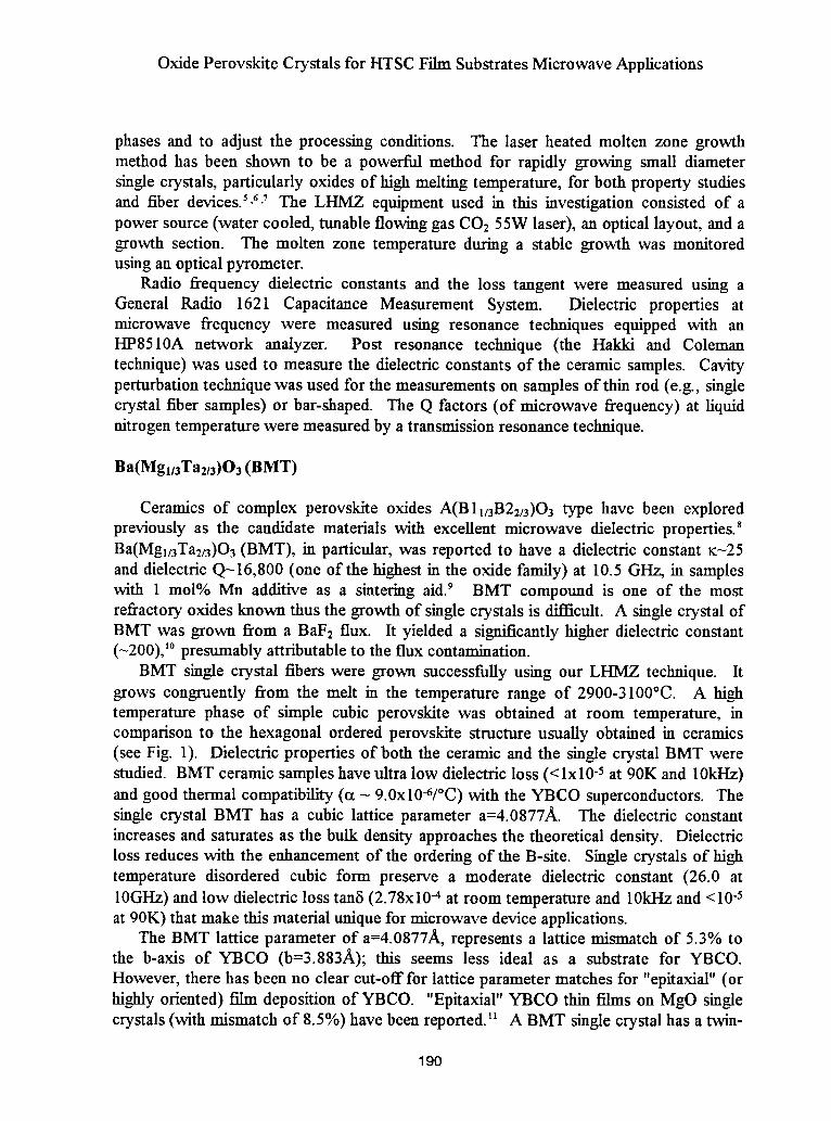
Oxide Perovskite Crystals for HTSC Film Substrates Microwave Applications
phases and to adjust the processing conditions. The laser heated molten zone growthmethod has been shown to be a powerful method for rapidly growing small diametersingle crystals, particularly oxides of high melting temperature, for both property studiesand fiber devices.5,6,7The LHMZ equipment used in this investigation consisted of apower source (water cooled, tunable flowing gas CO2 55W laser), an optical layout, and agrowth section. The molten zone temperature during a stable growth was monitoredusing an optical pyrometer.
Radio frequency dielectric constants and the loss tangent were measured using aGeneral Radio 1621 Capacitance Measurement System. Dielectric properties atmicrowave frequency were measured using resonance techniques equipped with anHP8510A network analyzer. Post resonance technique (the Hakki and Colemantechnique) was used to measure the dielectric constants of the ceramic samples. Cavityperturbation technique was used for the measurements on samples of thin rod (e.g., singlecrystal fiber samples) or bar-shaped. The Q factors (of microwave frequency) at liquidnitrogen temperature were measured by a transmission resonance technique.
Ba(Mgl/zTa2/3)O3 (BMT)
Ceramics of complex perovskite oxides A(Bll/3B22/3)O3type have been exploredpreviously as the candidate materials with excellent microwave dielectric properties.8Ba(Mgl/3Ta2/3)O3(BMT), in particular, was reported to have a dielectric constant _:-25and dielectric Q--16,800 (one of the highest in the oxide family) at 10.5 GI4_z,in sampleswith 1 mol% Mn additive as a sintering aid.9 BMT compound is one of the mostrefractory oxides known thus the growth of single crystals is difficult. A single crystal ofBMT was grown from a BaF2 flux. It yielded a significantly higher dielectric constant(-200), 1°presumably attributable to the flux contamination.
BMT single crystal fibers were grown successfully using our LHMZ technique. Itgrows congruently from the melt in the temperature range of 2900-3100°C. A hightemperature phase of simple cubic perovskite was obtained at room temperature, incomparison to the hexagonal ordered perovskite structure usually obtained in ceramics(see Fig. 1). Dielectric properties of both the ceramic and the single crystal BMT werestudied. BMT ceramic samples have ultra low dielectric loss (<lxl0 -5at 90K and 10kHz)and good thermal compatibility (cx- 9.0x10⁻⁶/°C)with the YBCO superconductors. Thesingle crystal BMT has a cubic lattice parameter a=4.0877,A,. The dielectric constantincreases and saturates as the bulk density approaches the theoretical density. Dielectricloss reduces with the enhancement of the ordering of the B-site. Single crystals of hightemperature disordered cubic form preserve a moderate dielectric constant (26.0 at10GHz) and low dielectricloss tank (2.78x10⁻⁴at room temperature and 10kHz and <10-5at 90K) that make this materialunique for microwave device applications.
The BMT lattice parameter of a=4.0877A, represents a lattice mismatch of 5.3% tothe b-axis of YBCO (b=3.883A); this seems less ideal as a substrate for YBCO.However, there has been no clear cut-off for lattice parameter matches for "epitaxial" (orhighly oriented) film deposition of YBCO. "Epitaxial" YBCO thin films on MgO singlecrystals (with mismatch of 8.5%) have been reported.I_ A BMT single crystal has a twin-
190
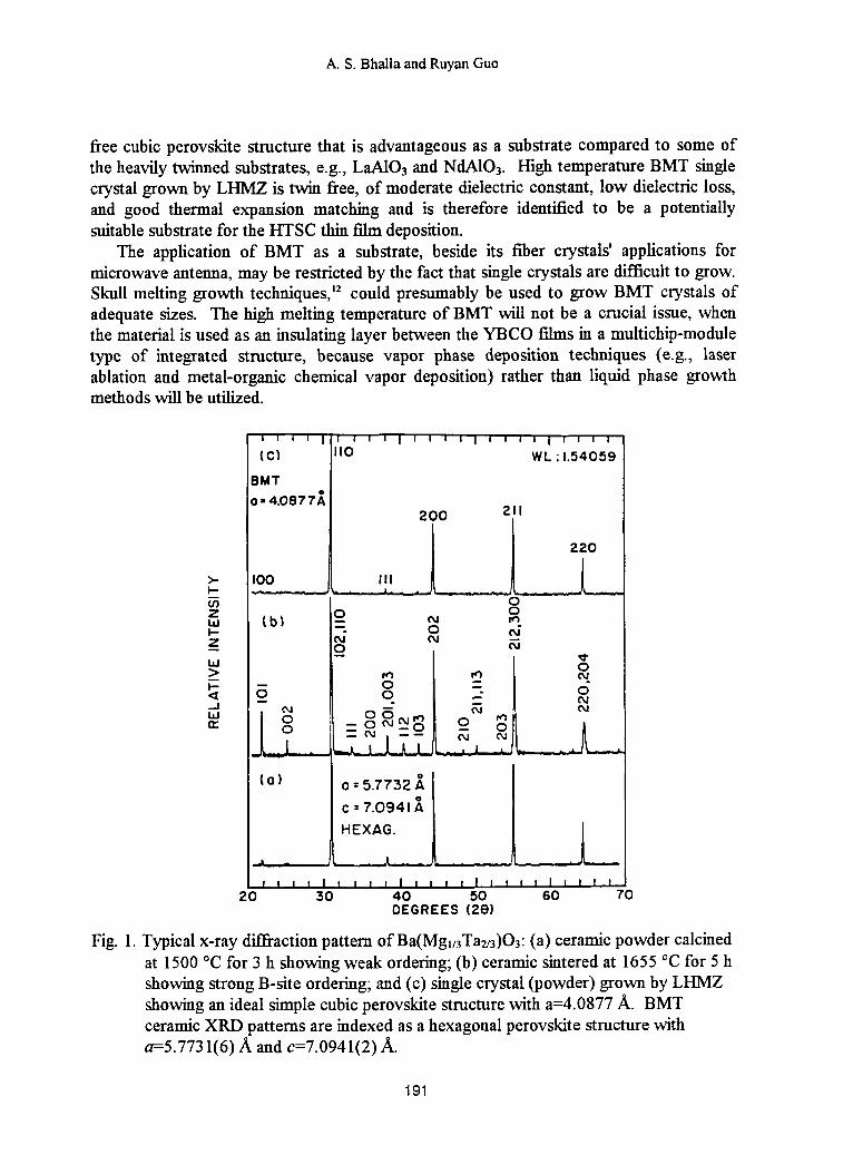
A. S. Bhalla and Ruyan Guo
free cubic perovskite structure that is advantageous as a substrate compared to some ofthe heavily twinned substrates, e.g., LaAIO3 and NdA103. High temperature BMT singlecrystal grown by LHMZ is twin free, of moderate dielectric constant, low dielectric loss,and good thermal expansion matching and is therefore identified to be a potentiallysuitable substrate for the HTSC thin film deposition.
The application of BMT as a substrate, beside its fiber crystals' applications formicrowave antenna, may be restricted by the fact that single crystals are difficult to grow.Skull melting growth techniques,_2could presumably be used to grow BMT crystals ofadequate sizes. The high melting temperature of BMT will not be a crucial issue, whenthe material is used as an insulating layer between the YBCO films in a multichip-moduletype of integrated structure, because vapor phase deposition techniques (e.g., laserablation and metal-organic chemical vapor deposition) rather than liquid phase growthmethods will be utilized.
I I i i i I i i I I I I I I | i I i I i I i i I
(C) I10 WL : 1.54059
BMTo • 4.0877A
200 211
,- ,00 'I'o
z 0 0
I- 0 c_J
r- a o° ----.I I 04 " O,,t
0: -o_-_ _ o__. L |
( o ) o =5.7732 _, /
lo
C=7.0941A
HEXAG. __
I I I I I I I I ! I I I I I I I I I I I i I I I20 30 40 50 60 70
DEGREES(2e)
Fig. 1. Typical x-ray dit_action pattern of Ba(Mgi/3Ta_3)O3:(a) ceramic powder calcinedat 1500 °12for 3 h showing weak ordering; (b) ceramic sintered at 1655 °C for 5 hshowing strong B-site ordering; and (c) single crystal (powder) grown by LHlVIZshowing an ideal simple cubic perovskite structure with a=4.0877 A. BMTceramic XRD patterns are indexed as a hexagonal perovskite structure witha=5.7731(6) A and c=7.0941(2)/_.
191
Oxide Perovskite Crystals for HTSC Film SubstratesMicrowave Applications
Sr(All/zTal/z)O_ (SAT) and Sr(All/2Nbl/2)O 3 (SAN)
The compounds of Sr(mll/2Tal/2)O3(SAT) and Sr(All/2Nbl/2)O3(SAN) were firstprepared and tested to learn their crystallographic phases and melting behavior by thegroup at the AT & T Bell Labs.13 Ceramic samples were identified to have double cellcubic perovskite structure with a=7.795A and melting temperatures of 1900°C and 1790°C for SAT and SAN, respectively. On the basis of our understandings of the crystalchemistry-dielectric property relation of various oxide perovskites, and the reports by theBell Labs group that showed both the SAN and SAT melt congruently and produce asingle phase of the perovskite structure after melting, we selected the SAT and SAN asprimary candidates in the A(Bll/2B2]:2)O3 complex oxide perovskite family for crystalgrowth and to investigate their properties in relation to substrate applications.
Sr(All/:Tal/2)O3 (SAT) and Sr(All/2Nbl/2)O 3 (SAN) are grown using the LHMZgrowth technique. Their crystallographic structures are found to be simple cubicperovskite with lattice parameters a=3.8952/_ (SAT) and a=3.8995A (SAN) that are ofclose lattice matching to the YBCO superconductors. No structural phase transitions ortwins have been found and the average coefficients of the thermal expansion are in goodmatching with the YBCO superconductor materials. SAT currently represents one of thebest potential HTSC substrate materials for microwave applications. The unique featureof this material is that it has desired dielectric properties (dielectric K-12, loss factortanS<10-4) at the microwave frequencies with twin-free lattice and good thermalexpansion matching along with chemical compatibility with the YBCO superconductors.Dielectric constants in RF region as measured on the dense ceramic samples of SAT andSAN at 23°C are shown in Fig.2.
22 ' I ' I ' I ' i ' I '
Temp.= 23 °C
_z SAN
Z0L)o 16
I.--
ttl.J,,, 13 SAT13
I00 , I , I , I , I , I J20 40 60 80 I00 120FREQUENCY(MHz)
Fig. 2. Dielectric constants of SAT and SAN ceramics as functions of frequency at roomtemperature.
192
A. S. BhaUa and Ruyan Guo
Our experimental results on the SAT composition along with the earlier report on thecongruent melting nature of the SAT and SAN compounds, have stimulated researchworks in the thin film area. MOCVD-derived SAT films grown at 850°C on LaAIO3 werefound to have exclusively (001) growth with in-plane orientation._4 Using SATpolycrystalline materials as targets in a pulsed laser deposition process, Findikoglu eta1.15.16have reported high quality epitaxial (c-axis orientation) growth of thin films ofSAT and multilayers of YBCO/SAT on (001) LaA103 and MgO substrates. Dielectricconstants of the SAT films (-100-390rim thick), however, were reported to be -23-30,notably higher than the value (_:-12) found in bulk ceramic materials. The deviationsfrom perfect cation stoichiometry in films may be one of the causes for the discrepancy invalue of the dielectric constants as the AFTa ratio in SAT films was found to be -0.8
rather than the stoichiometric ratio of unity. 12,_3No dielectric loss data has been reportedfor the SAT films therefore direct comparison between the dielectric constants of the filmand that of the bulk SAT sample is not intended.
SOLID SOLUTION OF TERNARY AND COMPLEX PEROVSKITE OXIDES
Further modification of the SAN and SAT compositions has been carded out to finetune their properties, particularly reducing-their melting temperatures (SAT:1900--(1908+25)13, and SAN:1790~(1739+10)13)_ for easier fabrication of the crystalsand bettercontrol of the reductionproblemof the Nb5+and Ta5+. Thismodificationwasalso an attempt to overcomethe twinningproblemand to stabilizethe cubicphase at roomtemperaturein LaAIO3crystals.
LaAlO3 has a rhombohedrally distorted perovskite (A3+B3+O3type) structure.Although the La3+ion generally prefers the 12-coordination-site,it has a tendency for9-coordination. The distortion in the LaOl: polyhedron is brought about by a slightdisplacementof the oxygen atoms away from the ideal positions of the cubic perovskiteform, that is more clearly shown in other [rear-earth]3+AlO3family members when theA-site cation radiibecome even smaller,e.g., in the case ofPrAlO3._8,_9 Fig. 3 presentsaclassificationof [A]3+[B]3+O3type compounds according to the constituent ionic radii(8-coordinationcation radiiwere used for A-site cations) focusing on the perovskiteregion.In fact, no ideal cubic perovskite structure but the rhombohedral[LaAlO3] and theorthorhombic [GdFeO3] structure have been reported in ternary compounds of the[A]3+[B]3+O3type.2° For aluminatecompounds, rhombohedralsymmetryis found whenA-site is occupied by the largest A3+cation, La3+,and other [A]3+[Al]3+O3compoundshave even lower symmetry
Ourapproachfollowing this directionwas to introduce "balanced" cation substitutionsimultaneously in the A- and B-sites to increase the average cation size at the A-site,hence to stabilize the 12-coordinationof that position and consequently the cubicperovskite structure. The solid solution of ternary LaAIO3and complex oxides ofSr(All/2Tal/2)O3or Sr(All/2Nbl/2)O3was chosenfor investigation.
By formingcrystallinesolutionswith compounds of low meltingtemperatures,it wasexpected that the crystalline solution would result in lower melting temperatureandconsequently avoid the reduction problem and permit growth in platinum crucibles.
193
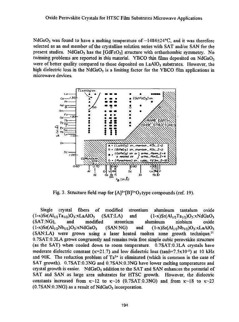
Oxide Perovskite Crystals for HTSC Film Substrates Microwave Applications
NdGaO3 was found to have a melting temperatureof-1484+_24°C, and it was thereforeselected as an endmember of the crystallinesolutionserieswith SAT and/or SAN for thepresentstudies. NdGaO3 has the [GdFeO3]structure with orthorhombic symmetry. Notwinningproblems are reported in thismaterial. YBCO thinfilms deposited on NdGaO3
were of better quality comparedto those depositedon LaAIO3substrates. However, thehigh dielectricloss in the NdGaO3is a limiting factor for the YBCO film applicationsinmicrowavedevices.
Fig. 3. Structure field map for [A]3+[B]3+O3 type compounds (ref. 19).
Single crystal fibers of modified strontium aluminum tantalum oxide(1-x)Sr(All/2TalI2)O3:xLa_O3 (SAT:LA) and (l-x)Sr(All/2Ta]/2)O3:xNdGaO3(SAT:NG), and modified strontium aluminum niobium oxide( 1-x)Sr(Al]/2Nb 1/2)O3:xNdGaO3 (SAN:NG) and ( 1-x)Sr(AI1/2Nb 1/2)O3 :xLRA10 3
(SAN:LA) were grown using a laser heated molten zone growth technique.2t0.7SAT:0.3LAgrows congruentlyandremainstwin freesimplecubicperovskitestructure(as the SAT) when cooled down to room temperature. 0.7SAT:0.3LAcrystals havemoderatedielectricconstant (K=21.7)andlow dielectricloss (tanS=7.Sxl0-s)at 10 kHzand90K. The reductionproblemof Ta5+is eliminated(whichis commonin the case ofSATgrowth). 0.7SAT:0.3NGand0.7SAN:0.3NGhave lowermeltingtemperaturesandcrystalgrowthis easier. NdGaO3additionto the SATandSANenhancesthe potentialofSAT and SAN as large area substratesfor HTSC growth. However, the dielectricconstants increased from _:-12 to ):-16 (0.7SAT:0.3NG) and from K:-18to _:-23(0.7SAN:0.3NG)as a resultof NdGaO3incorporation.
194
A. S. BhaUaand Ruyan Guo
Our results further confirmed the report of Mateika et al.= 23 that the ideal cubicphase can be formed in (La,Sr)(AI,Ta)O3 compounds. It is interesting to notice thatsimilar substitutions using [Ca,Ta] instead of [Sr,Ta] did not produce a compotmd withcubic structure. The average A-site cation radii of the [Ca,Ta] substitution is smaller thanthat of LaA103 (ionic radii of Ca2+, La3., and Sr2+ are 1.14, 1.185, and 1.27A,respectively),24therefore, no stabilization effect on 12-coordinationA-site is expected.
The cubic symmetry for the compound of SAT-NG and SAN-NG may be due to thefact that Ga3+is almost of the same cation size as TaS+/Nb5+. Slight reduction in theA-site cation size is accompanied by the slight increase of the B-site cation size and thusthe cubic structure of SAN or SAT stays intact.
The ideal cubic perovskite structure can be stabilized in the case of ternary LaAIO3byforming a crystalline solution composition with cubic Sr(All/:Tal/:)O3 andSr(All/:Nblr2)O3. The mechanism of this type of stabilization is through introducing thecompensated cation substitution in the form of [2La3+]+[AP+] _ [2A2+]+[B5+]with theA2+ cation having a radius larger than that of La3+ and therefore stabilifing the12-coordinatedA-site. Crystalline solutions of SAT-LA maintained or improved most ofthe dielectric and thermal properties of LaAIO3 and gained the advantage of forming atwin-free simple cubic structure and improved lattice compatibility. NdGaO3 is shown tobe an effective end member to decrease the melting temperature of SAN and SAT withoutdisturbing their simple cubic (twin-free) crystal structure. Dielectric constants of SANand SAT with addition of the NdGaO3 were increased; however, the dielectric loss factorstill remained less than 5x10⁻⁴. The results suggesting that SAT-LA and SAN-LA arebetter candidates as substrate materials than LaA103 because the latter is intrinsicallytwinned. The growth of SAT-NG and SAN-NG are comparatively convenient as theyhave relatively low melting temperatures together with the relatively lower dielectricconstants and the ideal lattice constants and thermal compatibility with the YBCOsuperconducting materials.
Other substrate candidates such as La(Mg:t3Tal/3)O3,:S La(Mgl/:Til/2)O3,26(Ca,Sr)(Ga,Nb)O327and a family of materials of the magnetoplumbite structures2s havealso been fabricated and their dielectric properties studied. These crystals and theirassociated solid solutions provide several new options for ultra low loss, low permittivity,twin free oxides with low congruent melting temperature, matching thermal expansion andexcellent chemical compatibility.
SUMMARY
Oxide crystals with the perovskite structure are major candidates for YBCO filmepitaxial deposition particularly if large size cubic, twin free crystals become available.SAT has already shown promise in high quality epitaxial YBCO film growth. Withimproved growth capability, the SAT and particularly its modified solid solutions may bemore useful than the intrinsically twinned LaA103. Solid solutions between the knowncomplex perovskite oxide and ternary end members, especially gallates, will provide largenumber of options to tailor the material for specific device applications. The property
195
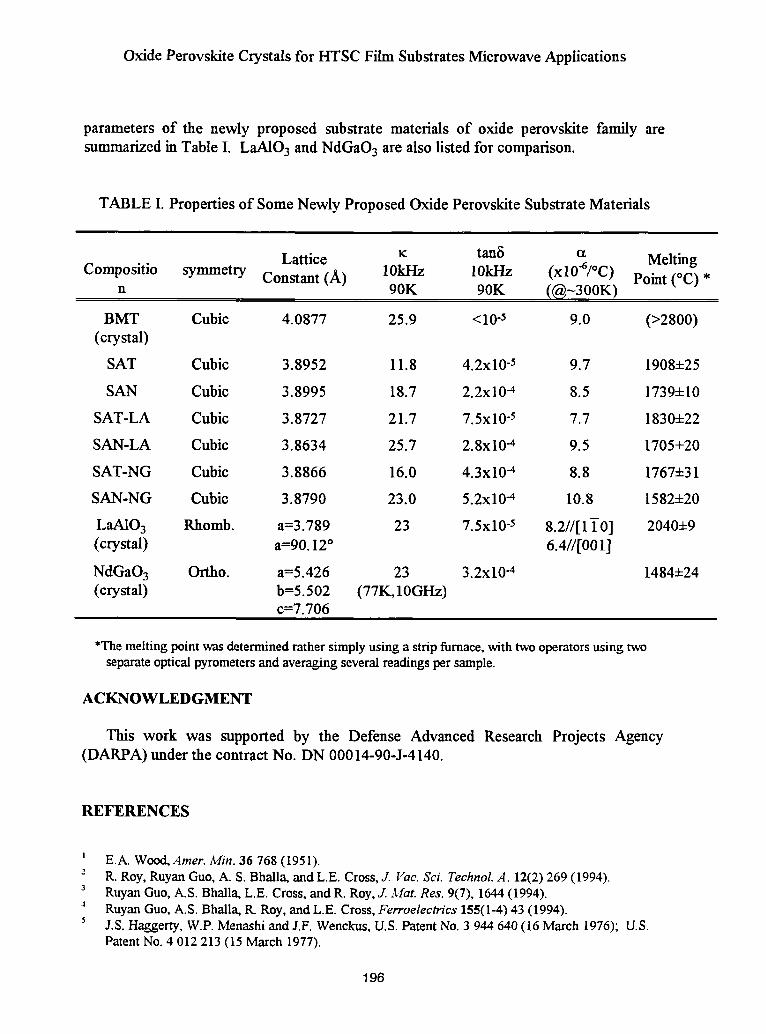
Oxide Perovskite Crystals for HTSC Film Substrates MicrowaveApplications
parameters of the newly proposed substrate materials of oxide perovskite family aresummarized in Table I. LaAIO3 and NdGaO3 are also listed for comparison.
TABLE I. Properties of Some Newly Proposed Oxide Perovskite Substrate Materials
Lattice K: tank ct MeltingCompositio symmetry Constant (A) 10kHz 10kI-Iz (xl0"6/°C) Point (°C) *
n 90K 90K (@-300K)
BMT Cubic 4.0877 25.9 <10.5 9.0 (>2800)(crystal)
SAT Cubic 3.8952 11.8 4.2x10⁴ 9.7 1908+25
SAN Cubic 3.8995 18.7 2.2x10⁻⁴ 8.5 1739+10
SAT-LA Cubic 3.8727 21.7 7.5x10⁻⁵ 7.7 18304-22
SAN-LA Cubic 3.8634 25.7 2.8x10⁻⁴ 9.5 1705+20
SAT-NG Cubic 3.8866 16.0 4.3x10⁻⁴ 8.8 1767+31
SAN-NG Cubic 3.8790 23.0 5.2x10⁻⁴ 10.8 1582+20
LaAIO 3 ghomb, a=3.789 23 7.5x10⁴ 8.2//[1T0] 20404-9(crystal) a=90.12" 6.4//[001]
NdGaO3 Ortho. a=5.426 23 3.2x10⁻⁴ 14844-24(crystal) b=5.502 (77K, 10GHz)
c=7.706
*The melting point was determined rather simply using a strip furnace, with two operators using twoseparateoptical pyrometers and averaging several readings per sample.
ACKNOWLEDGMENT
This work was supported by the Defense Advanced Research Projects Agency(DARPA) under the contract No. DN 00014-904-4140.
REFERENCES
E.A. Wood,Amer. Atin. 36 768 (1951).2 R. Roy, Ruyan Guo, A. S. Bhalla, and L.E. Cross, J. Vac. Sci. Technol. A. 12(2) 269 (1994).3 Ruyan Guo, A.S. Bhalla, L.E. Cross, and R. Roy, J. Mat. Res. 9(7), 1644 (1994).4 Ruyan Guo, A.S. Bhalla, R. Roy, and L.E. Cross, Ferroelectrics 155(1-4) 43 (1994).5 J.S. Haggerty, W.P. Menashi and J.F. Wenckus, U.S. Patent No. 3 944 640 (16 March 1976); U.S.
Patent No. 4 012 213 (15 March 1977).
196
A. S. BhaUa and Ruyan Guo
6 R.S. Feigelson, MRS Bull. 13 47 (1988).J. Yamamoto and A.S. Bhalla, Alat. Res. Bull. 24 761 (1989).
s K. Wakino, Ferroelectries 91 69 (1989).
9 S. Nomura, K. Toyama, and K. Kaneta, Jpn. J. Appl. Phys. 21(10) L624 (1982).l0 F. Galasso and J. Pinto, Nature vol. 207 No. 4992, 70 (1965).11
e.g., T. Terashima, K. Iijima, K. Yamamoto, K. Irata, Y. Bando, and T. Takada, Jpn. J. Appl. Phys.28, L987 (1989).
12 H.R. Harrison and J.M. Honig, Bull. Mater. Sci. 3(3), 247 (1981).13 C.D. Brandle and V.J. Fratello, J. Alater. Res. 5(10), 2160 (1990).14 B. Hart, D. A. Neumayer, B.H. Goodreau, T. J. Marks, H. Zhang, and V.P. Dravid, Chem. A/later. (in
press).
15 A.T. Findikoglu, C. Doughty, S. Bhattacharya, Qi Li, X.X. Xi, T. Venkatesan, R.E. Fahey, A.J.Strauss, and J. M. Phillips, Appl. Phys. Lett. 61 1718 (1992).
16 A.T. Findikoglu, S. Bhattacharya, C. Doughty, M.S. Pambianchi, Qi Li, X.X. Xi, S.M. Anlage, R.E.Fahey, A.J. Strauss, J.M. Phillips, and T. Venkatesan, IEEE Trans. Appl. Superconductivity, 3(1)1425 (1993).
_' R. Guo, A.S. Bhalla, J. Sheen, F. Ainger, E.C. Subbarao, S. Erdei, and L.E. Cross, J. Mat. Res. (inpress, 1994).
is R.D. Burbank, J. Appl. Cryst. 3 112 (1970)._9 O. Muller and R. Roy, in "The major ternary structural families" (Springer-Verlag, Berlin,
Heidelberg, New York 1974) p.215.20 F.S. Galasso, in "Structure. properties and preparation of perovskite-type compounds" (Pergamon
Press, Oxford. London, Edinburgh, Now York, Toronto, Sydney, Paris, Braunschweig 1969) p. 10.2_ R. Guo, P. Ravindranathan, U. Selvaraj, A.S. Bhalla, L.E. Cross, and R. Roy, J. Mater. Sci. (in press,
1994).
22 S. Haussiihl and D. Mateika, Crystal. Res. Technol. 26(4) 481 (1991).:3 D. Mateika, H. Kohler, H. Laudan and E. V61kel, J. Cryst. Growth 109 447 (1991).
24 R.D. Shannon and C.T. Prewitt, Acta Cryst. B25 (1969) 925; Acta Cryst. B26 1046 (1970).z_ P. Ravindranathan and A.S. Bhalla et al. (to be published).26 G. Harshe, A.S. Bhalla, and L.E. Cross, Materials Letters 18(4), 173 (1994).
27 S. Erdei, L.E. Cross, F.W. Ainger, and A.S. Bhalla, J. Cryst. Growth 139, 54 (1994).2s R. Guo and A.S. Bhalla (to be published).
197
Texturing of High Tc Superconducting Polycrystalline Fibers/Wires byLaser-Driven Directional Solidification in a Thermal Gradient
Usha VarshneyandB. DavisEichelberger, IIIAmericanResearch Corporationof Virginia
1509 Fourth Street, P. O. Box 3406Radford, Virginia 24143
ABSTRACT
This paper summarizesthe techniqueof laser-drivendirectionalsolidificationin acontrolledthermalgradientof yttria stabilizedzirconia core coated Y-Ba-Cu-O materialsto produce texturedhigh Tc superconductingpolycrystallinefibers/wireswith improvedcriticalcurrent densities in the extended range of magnetic fields at temperatures greaterthan 77K. The approach involves laser heating to minimize phase segregation by heatingvery rapidly through the two-phase incongruent melt region to the single phase meltregion and directionally solidifying in a controlled thermal gradient to achieve highlytextured grains in the fiber axis direction. The technique offers a higher grain growth rateand a lower thermal budget compared with a conventional thermal gradient and isamenable as a continuous process for improving the Jc of high Tc superconductingpolycrystalline fibers/wires. The technique has the advantage of suppressing weak-linkbehavior by orientation of crystals, formation of dense structures with enhancedconnectivity, formation of fewer and cleaner grain boundaries, and minimizationof phasesegregation in the incongruent melt region.
I. INTRODUCTION
Progress in the application of high critical temperature (Tc) ceramicsuperconductingpolycrystallinefibers/wires (with zero resistance above liquid nitrogentemperature at 77K) for very high speed system interconnects, integrated opticalcomponents and passive microwave devices for microelectronics and instrumentationapplicationsis currentlylimitedby the lack of formability,strength,toughness and lowtransport current properties. The low criticalcurrent densities(Jc) are associatedwithextremely smallcoherence length, causinggrainboundariesto act as Josephson junctionssuch thattunnelingcurrentsare highly fielddependent;a high degree of superconductivityanisotropy,severelysuppressingtunnelingcurrents at high-anglegrain boundaries;grainboundarysegregatedphases;andanisotropicthermalcontractionandmicrocrackingat thegrain boundaries. The causes of the weak link behavior can be greatly diminishedbydevelopmentof a process method which will yield formation of dense structures withenhancedconnectivity,crystallographictexturingof the grains, formation of cleaner andfewer grain boundariesparallel to the conduction direction, and minimizationof phasesegregation in the incongruent melt zone. One method of forming texturedmicrostructures is directionalsolidificationfrom the melt in a thermalgradient. However,in the Y-Ba-Cu-O system, the Y1Ba2Cu307 or 123 phase could not be obtainedcongruently from the melt of the 123 composition because of its incongruent
198
crystallization under the equilibrium phase transformation. The 123 phase is formed bythe peritectic reaction through the Y2BaCuO5 (211) phase and the liquid phase. If thecrystal-growth under the metastable state is realized, the peritectic reaction can besuppressed by rapid solidification with very high growth rate due to high interfaceundercooling and the 123 phase could be crystallized congruently resulting in highlyoriented fibers with improved grain boundaries and high Jc- In the 123 phase the criticalcurrent density is one order of magnitude higher along the a-b plane than along the c-axisdirection.
Research efforts have been directed toward increasing the Jc of high Tcsuperconducting materialsby texturing the grains using different techniques such as melttextured growth, liquid phase processing and directional solidification, quench and meltgrowth processes, and zone melting and laser float zone melting. All these techniqueshave resulted in highly textured microstructures (1). The significanceof the technique oflaser-drivendirectional solidificationin a controlled thermal gradient lies in its adaptabilityas a continuous process for improving the critical current densities of high Tcsuperconducting polycrystalline fibers/wires. The technical approach involves laserheating to minimize phase segregation by heating very rapidly through the two-phaseincongruent melt region (1010-1258°C) to the single phase melt region (> 1258°C) anddirectionallysolidifyingin a controlled thermal gradient to achieve highly textured grainsin the fiber axis direction.
H. EXPERIMENTAL TECHNIQUES
Texturing of extruded Y-Ba-Cu-O fiber, Duranickel 301(95%Ni • 4.4%Al • 0.6%Ti) core coated Dy-Ba-Cu-O and yttria stabilizedzirconia (YSZ)core coated Y-Ba-Cu-O high Tc superconducting polycrystalline fibers/wires wasinvestigated. Five cm long fiber segmentswere mounted on an alumina tube with the helpof alumina paste to hold the fiber and translated in a laser-driven directional solidificationthermal gradient (LDT) furnace as shown in Figure 1. The computer controlled LDTfurnace is comprised of a multiple heater array, a fiber translation mechanism capable oftranslating at rates of 0.5 to 200cm/hr, a fiber feed and fiber take-up system for feedingthe fiber preforms and removing the processed fibers, and a laser beam delivery systemconsisting of laser optics to homogeneously melt the fiber from four directions to thesinglephase melt zone. The LDT furnace consists of two split tube furnaces having 6.4cminternal diameter and eight independently computer controlled resistively heated zones.The upper split tube furnace consists of two heating zones, a 6.4cm long binder burnoutzone and a 10.2cm long preheat zone. The lower split furnace consists of six heatingzones, four 6.4cm long thermal gradient zones and two 10.2cm long annealing zones.Each zone is installed with a temperature sensor to provide flexibility in varying thetemperature profile in the thermal gradient. The furnaces are controlled by a closed loopcomputer based system. A 386-25MHz computer contains two data acquisition andcontrol boards to provide sixteen channels of differential analog input and cold junctioncompensation for thermocouple signals. An Inconel sheathed type-K thermocouple is
199
installed in the center of each furnacezone and connectedto one channelof the expansionsystem. The DT2815 data translationboard provides eight 4-20mA output channelstocontrol each thermal gradient zone using an Omega PCM1 4-20mA driver. LabtechNotebook sottware controls the furnace zones using a PID control algorithm. Eachthermocouple is sampled at a rate of 10Hz. LabtechNotebook also samples a ninththermocoupleat a slower rateandwrites thetemperatureto a datafile. By translatingthisthermocouplethroughthe furnaces,an exactprofileof the gradientcanbe recorded.
The thermalgradientfurnaceassemblyconsists of a fiber translationsystemwhichincludes a friction drive system to feed the fiber into the gradient and to remove theprocessed fiber (2-3). The LDT furnace is installedwith a laser beam delivery systemconsisting of laser optics to homogeneouslymelt the fiber from all directionsto the singlephase melt zone. This is accomplishedusing an 18 Watt CW Nd:YAG laser beam (_, =1.06Bm) which is evenly divided into 4 x 4.5 Watts, using beam splitters, mirrors andlenses arrangement as shown in Figure 2. The optics are mounted using an adjustableheight post system. Each post is fastenedto a micro optical rail to maintainalignmentbetween the components. The rails are mounted on an aluminum plate installedsurroundingthe furnace. A He-Ne laser and four pinhole apertureswere used to aligneach rail so as to focus the 4 x 4.5 Watt laser beam at the center of the laser zone,between the two split furnaces as shown in Figure 1, where the fiber is coaxiallytranslating. All the componentsare housed in a frame constructedfrom slotted steel angleiron and aluminumplates as shown in Figure 1. LabtechNotebook soi_ware has beenconfiguredfor controllingthe multipleheaterarray, fiber translationmechanism,fiber feedandfiber take-upmechanism. The fiberswere laser impactedwith a laser beam diameterof 2.5ram while translatingthrough the laser melt zone. The processed fibers werecharacterizedat the surface, as well as at the cross-section, using secondary electronimages on a PhillipsModel 505 SEM. The elementaldistributionand interdiffusionweredeterminedusing Philips Model PV 99W EDS energy dispersive X-ray analyzer. Thefibers were tested for critical temperature using flux exclusion technique and criticalcurrent densitiesusinga four probetechnique.
III. RESULTS AND DISCUSSION
Initially, extruded fibers of 123 materialswere investigated (1). The fragilecharacteristic of the processed fiber resulted in handling difficulty, therefore, core coatedhigh Tc superconducting fibers were identified as a more promising candidate for LDTprocess. Duranickel 301 (95%Ni • 4.4%A1• 0.6%Ti) core coated high Tcsuperconducting Dy-Ba-Cu-O fibers obtained from Pacific Superconductors weretranslated in the thermal gradient. Work was discontinued on the Duranickel 301 corecoated high Tc superconducting Dy-Ba-Cu-O fibers due to the interdiffusion of copper(Cu) and nickel (Ni) between the coating and the core at 800°C, which is below theperitectic melting temperature of high Tc superconducting Y-Ba-Cu-O materials, therebyresulting in destroying the superconducting property of the fiber (2-4).
200
Work was performed on yttria stabilized zirconia core coated high Tcsuperconducting Y-Ba-Cu-O fibers obtained from ICI superconductors. Figure 3 showsthe secondary electron image surface morphology of the yttria stabilized zirconia corecoated high Tc superconducting Y-Ba-Cu-O fibers along the fiber-axis direction. Figure3(a) shows the surface morphology of an unprocessed fiber. Figure 3(b) shows thesurface morphology of a fiber translated in the thermal gradient at a rate of 1.7cm/hr, inthe presence of 42.6ml/min flowing oxygen, with the laser melt zone temperature at1080°C. As seen from the micrograph elongated textured grains greater than 10x601amdimensionswere observed to extend in the direction of translation which is along the axisof the fiber. A high degree of crystal continuity and alignment was observed at theboundary region. Figure 4 shows the cross-sectional view of the yttria stabilized zirconiacore coated high Tc superconducting Y-Ba-Cu-O fiber. Figure 4(a) shows the secondaryelectron image of an unprocessed fiber. The core diameter is observed to be 8101am,whereas the coating thickness is observed to be 50ktm. Figure 4(b) and 4(c) shows thetypical energy dispersive X-ray (EDX) map of the elemental distribution of barium (Ba)and yttria (Y) over the fiber cross-section when processed under the parameters of Figure3(b). No elemental interdiffusion was observed between the coating and the core for allthe elements under consideration.
Figure 5 shows the secondary electron image surface morphology along the fiberaxis direction of the yttria stabilized zirconia core coated high Tc superconducting Y-Ba-Cu-O fibers translating at a rate of 1.7cm/hr in the thermal gradient, in the presence of42.6 ml/min flowing oxygen, with the laser melt zone temperature at 1020°C. Figure 5(a)shows the microstructure of a non-laser impacted zone of the fiber translated in thethermal gradient, whereas Figure 5(b) shows the surface morphology of the fiber impactedwith a laser radiance of 49W/cm2 while translating at a rate of 1.7 cm/hr in the thermalgradient with the laser melt zone temperature at 1020°C. By comparing Figure 3(b) and5(b) it can be observed that the laser-driven directional solidification in a controlledthermal gradient has a higher growth rate and a lower thermal budget than theconventional thermal gradient processing. Textured elongated grains in the fiber axisdirection can be observed at 1020°C as compared to 1080°C in the conventional thermalgradient. Besides having higher growth rates the significance of laser heating is thatcomplete melting to the single phase melt occurs in 53see, as compared to 10 hours byresistively heating, a time scale too short to allow significantsegregation under the drivingforce of the peritectic reaction. Figure 6 shows the final thermal profiles developed fromthe results obtained and are compared between resistively heated and laser heated to thesingle phase melt zone. Further considering the 53see time scale in the incongruent meltregion the intra-grain inclusions of Y2BaCuO5 will also be smaller so as to be beneficialfor flux pinning thereby improving the critical current properties of the high Tcsuperconducting polycrystalline fibers/wires for device applications. A superconductingcritical temperature was observed to be 80K in the processed fiber as compared with 95Kin the unprocessed yttria stabilized zirconia core coated high Tc superconducting Y-Ba-Cu-O fibers. A critical current densityof 1.8x10²Amps/cm2 at 77K, 0.6T was observed in
201
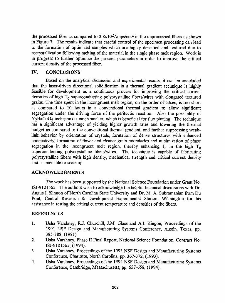
the processed fiber as compared to 2.8xl02Amps/cm2 in the unprocessed fibers as shownin Figure 7. The results indicate that careful control of the specimen processing can leadto the formation of optimized samples which are highly densified and textured due torecrystallization followingmelting of the material in the singlephase melt region. Work isin progress to further optimize the process parameters in order to improve the criticalcurrent density of the processed fiber.
IV. CONCLUSIONS
Based on the analytical discussion and experimentalresults, it can be concludedthat the laser-driven directional solidification in a thermal gradient technique is highlyfeasible for development as a continuous process for improving the critical currentdensities of high Tc superconducting polycrystalline fibers/wires with elongated texturedgrains. The time spent in the incongruent melt region, on the order of 53sec, is too shortas compared to 10 hours in a conventional thermal gradient to allow significantsegregation under the driving force of the peritectic reaction. Also the possibility ofY2BaCuO5 inclusions is much smaller,which is beneficialfor flux pinning. The techniquehas a significant advantage of yielding higher growth rates and lowering the thermalbudget as compared to the conventional thermal gradient, and further suppressing weak-link behavior by orientation of crystals, formation of dense structures with enhancedconnectivity, formation of fewer and cleaner grain boundaries and minimization of phasesegregation in the incongruent melt region, thereby enhancing Jc in the high Tcsuperconducting polycrystalline fibers/wires. The technique is capable of fabricatingpolycrystalline fibers with high density, mechanical strength and critical current densityand is amenableto scaleup.
ACKNOWLEDGMENTS
The work has been supported by the National Science Foundation under Grant No.ISI-9101565. The authors wish to acknowledge the helpful technical discussionswith Dr.Angus I. Kingon of North Carolina State University and Dr. M. A. Subramanian from DuPont, Central Research & Development Experimental Station, Wilmington for hisassistance in testing the critical current temperature and densities of the fibers.
REFERENCES
1. Usha Varshney, R.L Churchill, LM. Glass and A.I. Kingon, Proceedings of the1991 NSF Design and Manufacturing Systems Conference, Austin, Texas, pp.385-388, (1991).
2. Usha Varshney, Phase II Final Report, National Science Foundation, Contract No.ISI-9101565, (1994).
3. Usha Varshney, Proceedings of the 1993 NSF Design and Manufacturing SystemsConference, Charlotte, North Carolina, pp. 367-372, (1993).
4. Usha Varshney, Proceedings of the 1994 NSF Design and Manufacturing SystemsConference, Cambridge, Massachusetts, pp. 657-658, (1994).
202
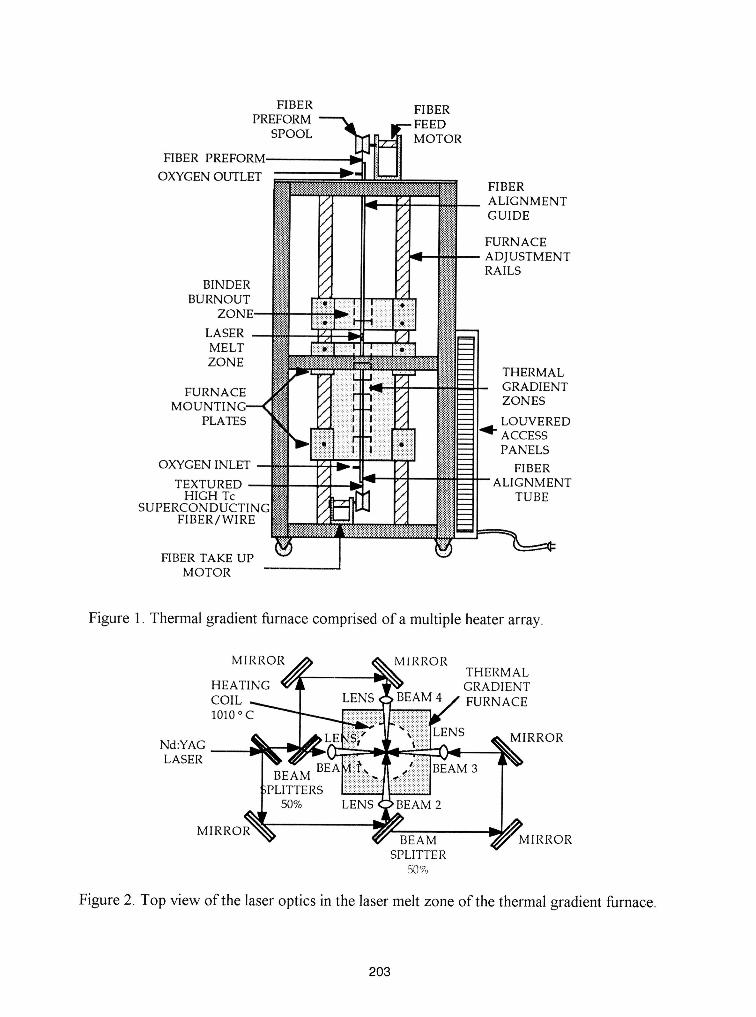
FIBER FIBERPREFORM
SPOOL MOTOR
FIBER PREFORM.
OXYGEN OUTLETFIBERALIGNMENTGUIDE
FURNACEADJUSTMENTRAILS
BINDERBURNOUT
LASERMELTZONE
THERMAL
FURNACE GRADIENTMOU ZONES
PLATES LOUVERED
PANELS
OXYGEN INLET FIBERTEXTURED ENT
HIGH Tc TUBESUPERCONDUCTING
FIBER/WIRE
FIBER TAKE UPMOTOR
Figure 1. Thermal gradient furnace comprised of a multiple heater array.
MIRROR MIRRORTHERMAL
HEATING GRADIENTCOIL FURNACE1010 oC
Nd:YAG MIRRORLASER
BEAM 3
50% LENS _BEAM 2
MI_ _BEAMSPLITTER
50%
Figure 2. Top view of the laser optics in the laser melt zone of the thermal gradient furnace.
203
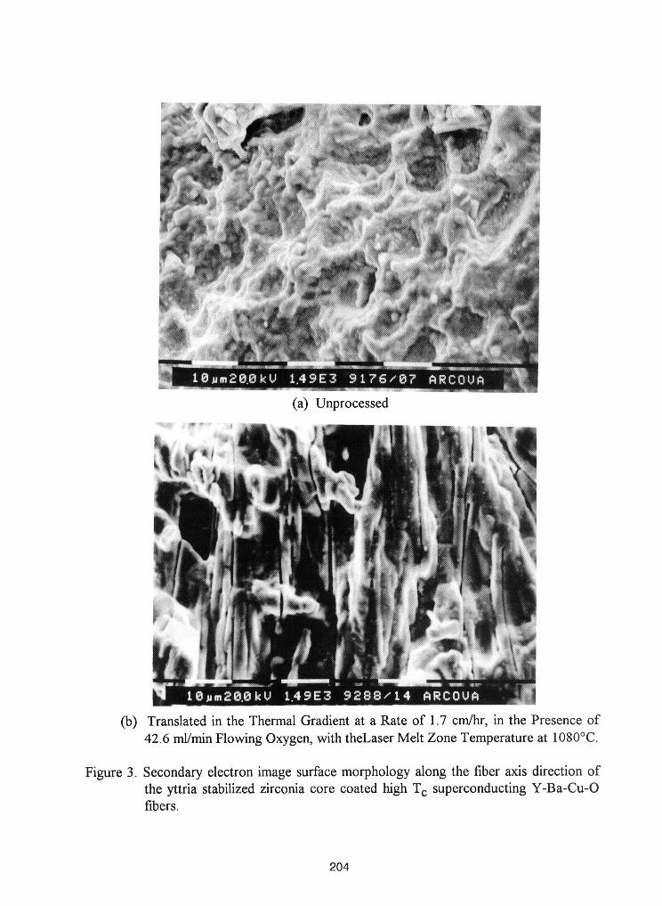
(a) Unprocessed
(b) Translated in the Thermal Gradient at a Rate of 1.7 cm/hr, in the Presence of42.6 ml/minFlowing Oxygen,with theLaser Melt Zone Temperature at 1080°C.
Figure 3. Secondary electron image surface morphology along the fiber axis direction ofthe yttria stabilized zirconia core coated high Tc superconducting Y-Ba-Cu-Ofibers.
204
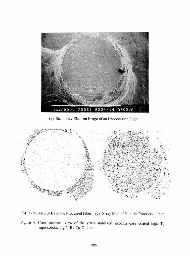
(a) SecondaryElectron Image of an UnprocessedFiber
(b) X-ray Map of Ba in the Processed Fiber (c) X-ray Map of Y in the Processed Fiber
Figure 4. Cross-sectional view of the yttria stabilized zirconia core coated high Tcsuperconducting ¥-Ba-Cu-O fibers.
2O5
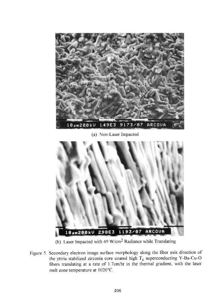
(a) Non-Laser Impacted
(b) Laser Impacted with 49 W/cm 2 Radiance while Translating
Figure 5. Secondary electron image surface morphology along the fiber axis direction ofthe yttria stabilized zirconia core coated high Tc superconducting Y-Ba-Cu-Ofibers translating at a rate of 1.7cm/hr in the thermal gradient, with the lasermelt zone temperature at 1020°C.
206
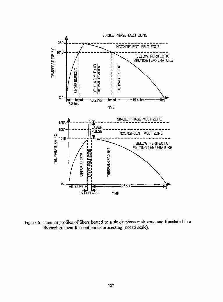
SINGLEPHASEMELTZONE
1080!
0 __CONGRUENT MELTZONE-pc/ ....... -_ .... _ELO-WPERTTo 1010- - 'ECTICILl
i:1:1,I n--__ _-
27 _" 1 r10.2hrs' ...- -... 9.4h s ""-i7.2 hrs
TIME
SINGLEPHASEMELTZONE1258 ' i_'
LASER
1080 'PULSE- INCONGRUENTMELTZONE(..)o
uJ,.r I t BELOWPERITECTIC
t t MELTINGTEMPERATUREluJIILl_ 181_ INI
I_.1LUI-- _ IhI_l
I:_I ._:
Z
! !I I
27 9.8hrs_ !4 27hrs53SECONI_S TIME
Figure 6. Thermal profiles of fibers heated to a single phase melt zone and translated in athermal gradient for continuous processing (not to scale).
207
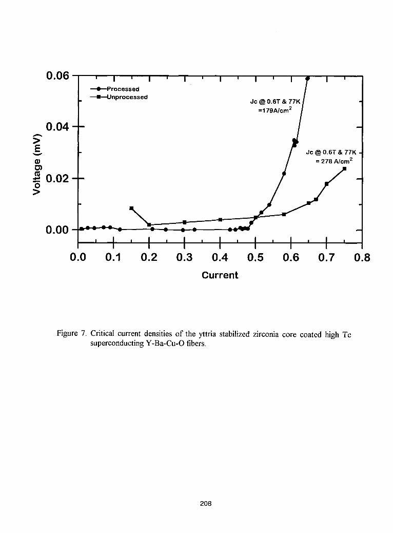
0.06' I ' I ' I ' I ' I ' I _ I '
_rocessed /
_ll_Unprocessed Jc @ 0.6T & 77K/
0.04 - =179AIcm2J/ Jc @ 0.6T & 77K
A AA -- 2
_0.02>
0.00' I ' I ' I ' I ' I ' I ' I '
0.0 0.1 0.2 0.3 0.4 0.5 0.6 0.7 0.8
Current
Figure 7. Critical current densities of the yttria stabilized zirconia core coated high Tcsuperconducting Y-Ba-Cu-O fibers.
208
HEAVY FERMION BEHAVIOUR EXPLAINED BY BOSONS
A. Kallio, S. Pfykk5 and V. ApajaUniversity of Oulu, Department of Theoretical Physics, Linnanmaa, SF-90570 Onlu, Finland
(May 27, 1994)
Abstract
Conventional heavy fermion theories require existence of massive fermlons. Weshow that heavy fermion phenomena can also be simply explained by existenceof bosons with moderate mass but temperature dependent concentration belowthe formation temperature TB, which in turn is close to room temperature. Thebosons B++ axe proposed to be in chemical equilibrium with a system of holes h+:B++ _-- h++h +. This equilibrium is governed by a boson breaking function f(T),which determines the decreasing boson density and the increasing fermion densitywith increasing temperature. Since HF-compounds axe hybridized from minimumtwo elements, we assume in addition existence of another fermion component h,+with temperature independent density. This spectator component is thought tobe the main agent in binding the bosons in analogy with electronic or muonicmolecules. Using a linear boson breaking function we can explain temperaturedependence of the giant linear specific heat coefficient 7(T) coming essentiallyfrom bosons. The maxima in resistivity, Hall coetTident and susceptibility axeexplained by boson localization effects due to the Wigner cryst_lll,ation. Theantiferromagnetic transitions in turn axe explained by similar localization of thepairing fermion system when their density nh(T_'r_)becomes lower than nw¢, thecritical density of Wigner cryst_lliTation. The model applies irrespective whethera compound is superconducting or not. The same model explains the occurrenceof low temperature antiferromagnetism also in high-To superconductors. Thedouble transition in UPt3 is proposed to be due to the transition of the pairingfermion liquid from spin polarized to unpolaxized state.
I. INTRODUCTION
Despite of the great efforts to understand heavy fermion (HF) properties [1-3] in terms ofconventional Fermi liquid theories [4-6], the Kondo model [7] or unconventional order param-eter models [8,9], the theories have not provided a clear overall picture of the most dramaticproperties: the large value and the temperature dependence of specific heat coefficient 7(T),the resistance maximum at low temperatures, the Hall coefficient and the susceptibility maximanear the same temperature. Likewise the superconducting states exhibit power law behaviorsof several quantities such as the specific heat near T = 0 and an additional linear term in thespecific heat. From the above reviews the following picture emerges: In the HF-compoundsthe f-electrons show localized behaviour at high temperatures and become delocalized at lowtemperatures. The point of division for the two behaviours is the Kondo temperature TK.
The purpose here is to show that the spectator fermion superfluid model (SFS), originallyproposed for high-To compounds [10,11] and the superfluid states of heavy fermions [12,13],also provides a global picture which connects the superfluid state with the normal state and,at the same time, explains the properties of non-superconducting HF-eompounds within thesame framework with bosons decaying into pairing fermions, the holes. Since the boson densityfor T >> Tc and the pairing fermion density for T _t: Tc both become small, they get local-ized due to Wigner crystallization [11,14]. In what follows we intend to show that the bosonlocalization temperature TBL < TB is in fact the coherence temperature corresponding to max-ima of Hall coefficient and susceptibility. Similarly the pairing fermion Wigner crystallization
2O9
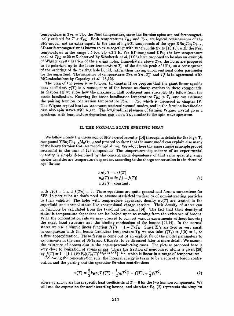
temperature is TFL = TN, the Ndel temperature, since the fermion spins are antiferromagnet-ically ordered for T < TFL. Both temperatures TBL and TFL are logical consequences of theSFS-model, not an extra input. In the case of high-To compounds of the type RBa2Cu3Or-x,3D-antiferromagnetism is known to exist together with superconductivity [15,16], with the Ndeltemperatures in the range 0.5 K< TN <2.2 K. For HF-compound UPt3 the low temperaturepeak at TFt. _ 20 mK observed by Schuberth et al. [17] is here proposed to be also an exampleof Wigner crystallization of the pairing holes. Immediately above TEL the holes are proposedto be polarized up to the lower temperature TZ of the double peak of UPt3 as a consequenceof the ordering of the pairing hole liquid, rather than having unconventional order parameterfor the superfluid. The sequence of temperatures TFL = TN, T_- and Tc+ is in agreement withMC-calculations by Ceperley et ai. [18,19].
The plan of the paper is as follows. In chapter II we propose that the giant linear specificheat coefficient 7(T) is a consequence of the bosons as charge carriers in these compounds.In chapter III we show how the maxima in Hall coefficient and susceptibility follow from theboson localization. Knowing the boson localization temperature TBL > To, one can estimatethe pairing fermion localization temperature TFL = TN, which is discussed in chapter IV.The Wigner crystal has two transverse electronic sound modes, and in the fermion localizationcase also spin waves with a gap. The longitudinal plasmon of fermion Wigner crystal gives aspectrum with temperature dependent gap below TN, similar to the spin wave spectrum.
II. THE NORMAL STATE SPECIFIC HEAT
We follow closely the discussion of SFS carried recently [14] through in details for the high-Tocompound YBa2Cu3-xMxO_-6 and proceed to show that the same model can explain also manyof the heavy fermion features mentioned above. We adopt here the same simple principle provedsuccessful in the case of 123-compounds: The temperature dependence of an experimentalquantity is simply determined by the concentration dependence of that same quantity, sincecarrier densities are temperature dependent according to the charge conservation in the chemicalequilibrium
nm(T) = nof(T)
nh(T)= 2n011- f(T)] (I)
n,(T) = constant,
with f(0) = 1 and f(TB) = 0. These equations are quite general and form a cornerstone forSFS. In particular we don't need to assume statistical mechanics of non-interacting particlesto their validity. The holes with temperature dependent density nh(T) are treated in thesuperfluid and normal states like conventional charge carriers. Their density of states canin principle be calculated from the two-fluid formalism [14]. The fact that their density ofstates is temperature dependent can be looked upon as coming from the existence of bosons.With the concentration rule we may proceed to connect various experiments without knowingthe exact band structure and the binding mechanism of the bosons [11,14]. In the normalstates we use a simple linear function f(T) = 1 - T/TB. Since Tc's are zero or very smallin comparison with the boson formation temperature TB we can take f(Tc) ,_ f(0) = 1, asa first approximation. These features come out of an explicit fit of the model parameters toexperiments in the case of UPts and URu2Si2, to be discussed later in more detail. We assumethe existence of bosons also in the non-superconducting cases. The picture proposed here isvery close to ionization of atoms in gas. There the fraction of non-ionized atoms is given [20]
512 2_IkBT t/2by f(T) = 1 - [1 + (P/Po)(To/T) e ]- , which is linear in a range of temperatures.Following the concentration rule, the internal energy is taken to be a sum of a boson contri-
bution and the pairing and the spectator fermion contributions
1 2u(T) = 3kBnoTf(T) + 17hT211 - f(T)l + iT, T, (2)
where7h and7,arelinearspecificheatcoefficientsatT = 0forthetwofermioncomponents.We
willusetheexpressionfornoninteractingbosons,and thereforeEq. (2)representsthesimplest
210
approximationone can thinkof.Forf = 0 thisreducestotheconventionaltwo fermionresultandforf = Iwe obtainthefreebosonand thespectatorcontributions.Inthenormalstatethisexpressionissupposedtobevalidonlydown tofinitetemperaturesnearTcwherethesuperfluidfluctuationsbecome important.Inthesuperconductingstateone may usetheexpression(2),exceptthatthebosonpartisreplacedby theacousticplasmoncontributionto be discussedlater. In the BCS-like situation (TB = To, no plasmon sound) we have f(T) = n,(T), where thesuperfluidfractionbehavesexponentially,n, _. 1- e"(1-1p), with t = T/Tc, Eq.(2) reproducesthe typical BCS result with a step in the specificheat at To. The expression(2) is thereforereasonablein the threespecialcasesf - 1,f = 0 and f = n,. Weanticipatethat the calculationof boson breakingfunction f(T) is in principlepossibleonceweknow the details of the bosonbinding,the bandstructureandthechemicallattice.Sofarwearecontentto assumethat thespectatorsplayan essentialrolein the binding[14].In viewof the fact that the compoundsweareworkingwith arerather complicated,wethereforeshoulduse a formalism,simple enough,to enableone to relate variousexperimentswith a reasonableaccuracyas was donein Ref.[14]forthe 123-case.In what followswe intendto showthat alsotheheavy fermionscan betreatedin this spirit and the resultsturn out to be equallygood.
Eq.(2) givesfor the normalstate the specificheat coefficient
c(T) 3k °(1 _--) + _-ra_-_B, (3)7(T) -_ 2 T n T 3 T: _ -2usingthesimplelinearfunctionforf(T).At lowtemperaturesthebosoncontributiondomi-nates,sinceTB _ 300--500 K, and atlowtemperatures(T < 20 K) we obtain
A
7(T) : 7, + _. (4)
This also shows, how the spectators give the linear term in the specific heat in the supercon-ducting state at T -- 0. At the temperature T8 the linear term reads
37(T) : 7° + _Th. (5)
Above TB we obtain the normal metallic behaviour 7(T) = 7° + 7h. Immediately below TBwe obtain linear behaviour and a step at TB. We anticipate that m_ >> m_, therefore thecontribution from the pairing fermions 7h should dominate at room temperature. On the otherhand, already at much lower temperature the boson contribution gets small as compared withfermion parts, therefore one may be able to separate the contributions from 7h and 7,, since thelatter one can be obtained at least in the superconducting situation from the measurements nearT = 0. Near the localization temperatures TB£ and TFL these expressions have to be modifiedin a way to be discussed later. In particular the boson term cannot continue down to zerotemperature but is intruded by the superconducting or the antiferromagnetic transition. Sincethese are ordered states, the boson contribution is replaced below the ordering temperature bythe plasmon sound or spin wave contributions, which will give finite entropy.
We have compared the electronic specific heat coefficient 7(T) from Eq. (4) with experimentsin Fig. 1 a) for UBel3 and CeCu2Si2 and in Fig. 1 b) for CeAl3 and CeCu6. These figures arebased on figures (6) and (16) of Stewart [2]. It is seen that this simple theory gives a satisfactoryexplanation for the observed behaviour of 7(T) in these four cases. The coefficients A comeout to be nearly the same A ._ 1400 mJ/Kmol corresponding to boson densities of the order1021cm-3. One obtains this order of magnitude also from the the analysis of the Hall-data,as we shall see. The model therefore proposes that the large size of 7(T) is due to the bosonsrather than fermions. This means also that the fermions need not be excessively heavy, which isdesirable, since band structure calculations do not produce excessively narrow bands required bythe conventional heavy fermion theories (see Ref. [4], p. 121). In fact the bandwidths obtainedfrom band calculation are two orders of magnitude larger.
The compounds in Fig. 1 a) become superconducting at very low temperatures, but those inFig. 1 b) do not. This simple theory should apply to both types. As we shall see the presentmodel predicts a glassy antiferromagnetic transition at very low temperatures so that 7(T)is cut off. For CeAIa this is clearly visible (see Ref. [2], Fig. 15) but for CeCu6 less so. At
211
present we are not able to determinethe fermioneffectivemasses veryaccurately. There issome uncertaintyassociatedwith the possiblenon-linearitiesin f(T) whichno doubt can beestimatedeasily,but goes beyondthe scopeof this paper. ClearlyEqs. (2)-(5) cannotbe validdownto zero temperature,as mentionedabove. Forsuperconductingcompounds"r(T)nearTcis modifiedby superconductingfluctuationsand belowTc the plasmoniccontributionreplacesthe freebosonpart. Fornon-superconductingcompoundsthesuperconductingfluctuationsmayexist near T -- 0. Theorderedtransitions at Tc or TFL m TN seemto offer a natural cut off formost HF-compounds.
s) b) 100(
_"Pi800 UBeI$
_l,..400 %
200 200 -. _-f..,... _
0 00 I0 20 30 40 50 60 0 30 60 90 120
FIG. 1. The electronic specific heat coefficient "r(T) for a) UBe13 and CeCu2Si2 and b) CeAh andCeCu6. Solid lines presents our theoretical result from Eq. (4) with parameters: a) A = 1300mJ/molKand "r, --_5mJ/molK 2 and b) A ----1500mJ/molK and _° _ 140mJ/molK 2. Experimental points arefrom Figs. 6 and 16 in Ref. [2].
III. BOSON LOCALIZATION
A logicalconsequenceof theSFSmodelis theWignercrystallization(WC)ofbosons,becauseat a certaintemperatureTBL, whichliesin betweenT¢ and TB, theirdensitydiminishesbelowthe critical valuecorrespondingto r, = 170 [19]. The localizationtemperatureTBL can beestimatedfrom the conditionfor the criticaldensity,
nw° nof(rBL)no(l--T.n/r.).O.16.102`---- cm -a, (6)
where m is the electron mass and the boson mass mB -- 2ms. This order of magnitudeestimate corresponds to a jellium background and may be inaccurate for backgrounds prevalentin the heavy fermions with spectators and the chemical lattice. Most likely, however, sucha transition does take place, and the main consequence is that the bosons become graduallydelocalized below TBL. The measured carrier densities in HF-compounds are of the order ofmagnitude 1021cm-a [6], close to those required by Eq. (6). Above TBL the bosons cease to beactive charge carriers.
A fully consistent thermodynamical description of the localization is not attempted here forthe following reasons: Above TBL the bosons continue to decay into holes with approximatelylinear temperature dependence, as deduced from Hail-measurements. Because of this decay,the Wigner crystal is never complete. Since the boson localization phenomena occur at mod-erately low temperatures, the Wigner crystal is never in thermal equilibrium, and one expectsa glassy behaviour. The situation is further complicated by the lattice which can cause par-tial localization of the bosons even below TBL. This is presently the main uncertainty whichclearly affects our calculation of the coefficient A in Eq. (4) with density no deduced from theHall-measurements.
The Monte-Carlo-calculations by Ceperley et al. [18,19] indicate, that the energy densities ofCoulomb liquid and crystal states are not very different, therefore the associated specific heatjump may be small at elevated temperatures. For these reasons the liquid-crystal transition isvery rounded and shows up most clearly in the Hall density which well above TBL is determinedsolely by the holes. This explains the near linearity of nH (T) observed in virtually all compounds
212
above the coherence temperature, which we associate here with TB_. We actually do notexactly know what f(T) to use between Tc and TBL, therefore we have used the followingpurely phenomenological description: Divide the density of bosons below TBL into localizedand delocalized portions with a phenomenological function _(T) such that the density of mobilebosons is
nBDL(T) = nof(T)_(T) .._n0(1 - T/TB) _(T), (7)
where _ = a _< 1 for T << TBL and _ = 0 for T >> TBL. Here a < 1 means that a fraction(1 - a) of the bosons remain localized for T << TBL. Localized bosons continue to produceholes with linear rate f(T). This was previously [14] used successfully to explain the Hall effectin the high-T_ case. The existence of bosons in the normal state was also used to explain the"reservoir" effect for 123-compounds.
The function _(T) can be obtained from the experimental Hall coefficient R.b o¢ nh(T) -1.The effective Hall density (in the ab-plane) reads
2n0(1 - f(T)) _- 2noT_, for T :_ TBLnH= 2n0(1 f(T)) + 2nof(T)_(T) _- 2n0T_ + 2n0(1 -- T/TB)_(T), for T <_TBL. (8)
These equations together with the Hall-measurements can be used to fix TB as well. Thelocalization explains the minimum in nfI, a feature which seems to be as common for heavyfermions as it is for high-To superconductors [14]. We have shown for 123 compounds [14] thatf(T) is a universal function.
The Hall density in the normal state together with the experimental data of Lapierre etaL [21] and Schoenes et al. [22] is shown in Figs. 2 a) and 2 b). The theoretical curve in Fig. 2a) for UPt3 was calculated using Eqs. (8) with the phenomenological boson localization factorof the type
[ (r--6-K-' I_(T)=exp 3.5 \T_ 50 Klj ,6K<T<50K. (9)
Similar function was used also for URu_Si2 in Fig. 2 b).
l) 12 I
J
, 'I 7"6 4 '
,Jo
30 41Q 60 80 I_0 120 140 IfJO 180 _0 _0 0 _10 100 ISO 200 2.50 _ 350
T(K) T(g)
FIG. 2. a) The Hall density in the normal state for UPt_ from Eq. (8) together with the experi-mentd data of Lapierre et al. [21]. Theoreticd result is obtdned by using parameters: T_ ----500 K,fc ----.88, no = 4.95- 1021cm-s _nd a ----1. b) The Hall density in the normM state for URu2Si2from Eq. (8) together with the experimental data of Schoenes et al. [22]. Theoretical result is obtainedby using paxametets: TB ----350 K, f¢ = .98 _nd no ----5.7 • 1021cm-3 and boson localization factor
i'/ x'l
14(T--18 K')] for 18 K <T< 110 K._(T) ----.36- exp
We overlook the further complication, that the spectators could bring in a more complicatedtwo-band Hall behaviour. The fact that, Hall coefficient with H J _ is nearly constant whereasthe one with H II_ changes with temperature above TBL [23], gives evidence that band mixingis small, therefore this point is not fully understood at present. The outcome of Eq. (8) for
213
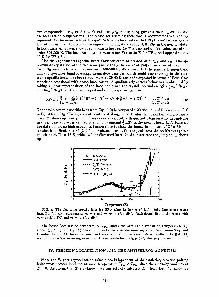
two compounds, UPta in Fig. 2 a) and URu2Si2 in Fig. 2 b) gives us their Ts-values andthe localization temperatures. The reason for selecting these two HF-compounds is that theyrepresentthe two main cases with respect to fermionlocalization: In UPt3 the antiferromagnetictransition turns out to occur in the superconductingstate and for URu2Si2in the normal state.In both cases nit-curves show slight upwardsbending forT > TBL and the TB-values are of theorder 300-500 K. The localization temperatures are TSL ,_,30 K for UPta and approximately50 K for URu2Si_.
Also the experimental specific heats show structure associated with TBL and TB. The ap-proximate separation of the electronic part AC by Renker et al. [24]shows a broad maximumfor UPt3 near 30-40 K and a peak near 300-500 K. We expect that the pairing fermion bandand the spectator band rearrange themselves near TB, which could also show up in the elec-tronic specific heat. The broad maximum at 30-40 K can be interpreted in terms of Bose glasstransition associated with boson localization. A qualitatively correct behaviour is obtained bytaking a linear superposition of the Bose liquid and the crystal internal energies _nB(T)kBTand 3nB(T)kBT for the boson liquid and solid, respectively,hence
AC = [ _nokB--_ [Tf(T)(2 - _(T))] + 7.T + -_'rhIt - f(T)] T , for T < TB (lO)L(Ts + 7h)T , for T > TB "
The total electronic specific heat from Eqs. (10) is compared with the data of Renker et ai. [24]in Fig. 3 for UPt3. The agreement is rather striking. In particular the boson formation temper-ature TB shows up clearly in both compoundsas a peak with quadratic temperature dependencenear TB. Just above TB we predict a jump by amount ½7hTBin the specificheat. Unfortunatelythe data do not go high enough in temperature to show the jump. In the case of URu2Si2oneobtains from Renker et ai. [24] similar picture except for the peak near the antiferromagnetictransition at TN = 18 K, which will be discussed later. In the latter case the jump at TB showsup.
12
10
8
o 6
4
J2
o1 lO 1oo 1ooo
Temperature(K)FIG. 3. The electronic specific heat for UPtz after Renker et al. [24]. Solid line is our result
from Eq. (10 with parameters: 3', = 0 and 7h = 16mJ/molK2. Dash-dotted line is the result with7, = 4mJ/m olK_ and 7h = 16mJ/molK_.
The boson localization temperature TBL limits the attainable transition temperature T¢,since TSL > Te. By Eq. (6) one should make the effective mass mh small to increase TBL andthereby the To. At the same time the backgroundcan also have a decisive effect. In Ref. [14]we found effective mass mh "_m_ and the estimate for UPt3 is 5-20 electron masses.
IV. FERMION LOCALIZATION AND THE ANTIFERROMAGNETISM
Since the Wigner crystallization takes place independent of the statistics, also the pairingholes must become localized at some temperature TFL < TBL, since their density vanishes atT = O. Assuming that TBL is known, we can actually calculate TFL from Eqs. (1) since the
214
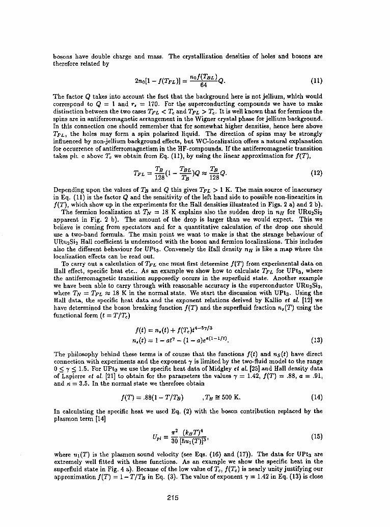
bosons have double charge and mass. The crystallizationdensitiesof holes and bosons aretherefore related by
2no[1 - f(TFL)] -- no.f(TBL) Q. (11)64
The factor Q takes into account the fact that the background here is not jellium, which wouldcorrespond to Q = 1 and ro = 170. For the superconducting compounds we have to makedistinction between the two cases TFL < T_ and TF£ > T_. It is well known that for fermions thespins are in antiferromagnetic arrangement in the Wigner crystal phase for jellium background.In this connection one should remember that for somewhat higher densities, hence here aboveTFL, the holes may form a spin polarized liquid. The direction of spins may be stronglyinfluenced by non-jellium background effects, but WC-localization offers a natural explanationfor occurrence of antiferromagnetism in the HF-compounds. If the antiferromagnetic transitiontakes pin e above Tc we obtain from Eq. (11), by using the linear approximation for f(T),
TB (1 - TBL )Q _ TB Q (12)TFL=Depending upon the values of TB and Q this gives TFL > 1 K. The main source of inaccuracyin Eq. (11) is the factor Q and the sensitivity of the left hand side to possible non-linearities inf(T), which show up in the experiments for the Hall densities illustrated in Figs. 2 a) and 2 b).
The fermion localization at TN -- 18 K explains also the sudden drop in nH for URu2Si2apparent in Fig. 2 b). The amount of the drop is larger than we would expect. This webelieve is coming from spectators and for a quantitative calculation of the drop one shoulduse a two-band formula. The main point we want to make is that the strange behaviour ofURu2Si2 Hall coefficient is understood with the boson and fermion localizations. This includesalso the different behaviour for UPta. Conversely the Hall density nH is like a map where thelocalization effects can be read out.
To carry out a calculation of TF£ one must first determine f(T) from experimental data onHall effect, specific heat etc.. As an example we show how to calculate TFL for UPt3, wherethe antiferromagnetic transition supposedly occurs in the superfluid state. Another examplewe have been able to carry through with reasonable accuracy is the superconductor URu2Si2,where TN ----TFL _. 18 K in the normal state. We start the discussion with UPta. Using theHall data, the specific heat data and the exponent relations derived by Kallio el aL [12] wehave determined the boson breaking function f(T) and the superfluid fraction n,(T) using thefunctional form (t = T/T€)
f(t) = n,(t) + I(To)t 4-5_/3
n,(t) = 1 - at "1- (1 - a)e _O-11t). (13)
The philosophy behind these terms is of course that the functions f(t) and ns(t) have directconnection with experiments and the exponent "r is limited by the two-fluid model to the range0 < 7 < 1.5. For UPta we use the specific heat data of Midgley et al. [25] and Hall density dataof Lapierre et al. [21] to obtain for the parameters the values 7 = 1.42, f(T) = .88, a = .91,and _€= 3.5. In the normal state we therefore obtain
f(T) = .88(1 - T/TB) ,TB _--500 K. (14)
In calculating the specific heat we used Eq. (2) with the boson contribution replaced by theplasmon term [14]
_r2 (kBT)4 (15)upz- 30[hu(T)p'
where ul(T) is the plasmon sound velocity (see Eqs. (16) and (17)). The data for UPta areextremely well fitted with these functions. As an example we show the specific heat in thesuperfluid state in Fig. 4 a). Because of the low value of To, .f(Tc) is nearly unity justifying ourapproximation f(T) = 1 -T/TB in Eq. (3). The value of exponent 3' = 1.42 in Eq. (13) is close
215
to the one obtained for 123 in Ref. [14] (7 = 1.3) as well as the gap parameter _ = 3.5 insteadof 3. The small coefficient .09 in front of the gap term makes n, (t) to have nearly power-lawbehaviour. The most dramatic difference between the HF. and high-To compounds is the pairbreaking at Tc which gives fc _ 1 for former and fc _ .6 for the latter. For URu2Si2 it comes outclose fc -_ .98. The physical explanation for this is the low value of Tc for HF-compounds. Theheavy fermions are therefore further away from the BCS than the high-To superconductors, inview of the fact that within the present framework fc = 0 for BCS. Since the boson densities arenot very different for the high-To and HF-compounds, simple Bose-Einstein model for heavyfermions would give, with moderate boson mass mB < 10me, right order of magnitude forTc [14,26]. Without boson breaking this model would, however, have difficulties in explainingthe localization phenomena discussed here.
a) b) i_
o
o .1 .2 .1 .4 .5 ._; o 0 .2 .4 .6 .I IT (K) T/T€
FIG. 4. a) The experimental specific heat for UPta from Ref. [25] together with our theoreticalresult. For f(t) we have used parameters: fc = .88, "t= 1.42, a = .91 and _ = 3.5. The used spectatorcontribution 3',= 130m-l/molK2 is muchlarger than the one obtained from Fig. 3. b) The experimentalspecific heat for URu_Si2 from Ref. [30] together with our theoretical result. For f(t) we have usedparameters: fc = .98, 7 = 2.16, a = .987 and _ = 3.6. The spectator contribution comes out to be7, = 23mJ/molK 2.
Knowing the boson breaking function f(T) for UPt3 we can now calculate the Wigner crys-tallization temperature TFL for the holes to be about 20 inK, close to the experimental value18 mK found for the extra peak by Schuberth et al. [17]. Our result is obtained from Eq. (11)with Q = 1. Since in the Wigner crystal for the holes the spins are in the antiferromagneticarrangement,we proposethatTFL = TN, the N_eltemperature.
Although the properties of the antiferromagnetic transition may be affected by the chemicallattice, we may explain some properties, like the specific heat peak, by the Wigner crystalmodel below Tlv. Since the transition takes place at low temperatures, we may use the soundmode approximation for the WC specific heat. The excitation modes of WC have been studiedtheoretically by Carr [27]. According to his calculations the Wigner crystal has two transversal
sound modes, with the density dependent sound velocities u_ cc r71/_. In the present case thistranslates into the temperature dependence [14]
Uj.(TFL) r 1 _ f(T) ] 1/6 (16)U.l.(T)L1 - f(TFI,)J "
In the case of pairing fermions forming a liquid, the longitudinal sound velocity ul(T) wasdetermined by the relation
r'-.f(r)11":'ul(T) = ul(Tc) LX-/-'_-_)J " (17)
Despite of the pairing fermion localization the two-fluid philosophy remains the same: Thenormal liquid density in the superfluid system consisting of bosons and holes, is obtained fromthe bosonic (sound modes, spin waves) and fermionic excitations (boson breaking). The latterones are determined by [1- f(T)] which should be determined by the chemical equilibrium, but
216
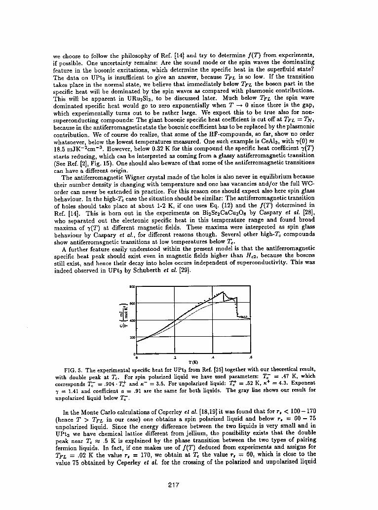
we choose to follow the philosophy of Ref. [14] and try to determine f(T) from experiments,if possible. One uncertainty remains: Are the sound mode or the spin waves the dominatingfeature in the bosonic excitations, which determine the specific heat in the superfluid state?The data on UPts is insufficient to give an answer, because TFL is so low. If the transitiontakes place in the normal state, we believe that immediately below TFL the boson part in thespecific heat will be dominated by the spin waves as compared with plasmonie contributions.This will be apparent in URu2Si_, to be discussed later. Much below TFL the spin wavedominated specific heat would go to zero exponentially when T -- 0 since there is the gap,which experimentally turns out to be rather large. We expect this to be true also for non-superconducting compounds: The giant bosonic specific heat coefficient is cut off at TFL = T_r,because in the antiferromagnetic state the bosonic coefficienthas to be replaced by the plasmoniccontribution. We of course do realize, that some of the HF-compounds, so far, show no orderwhatsoever, below the lowest temperatures measured. One such example is CeAIs, with 7(0) _.18.5 mJK-2cm -3. However,below 0.32 K for this compound the specific heat coefficient 7(T)starts reducing, which can be interpreted as coming from a glassy antiferromagnetic transition(See Ref. [2], Fig. 15). One should also beware of that some of the antiferromagnetie transitionscan have a different origin.
The antiferromagnetic Wigner crystal made of the holes is also never in equilibrium becausetheir number density is changing with temperature and one has vacancies and/or the full WC-order can never be extended in practice. For this reason one should expect also here spin glassbehaviour. In the high-T_ case the situation should be similar: The antiferromagnetic transitionof holes should take place at about 1-2 K, if one uses Eq. (12) and the f(T) determined inRef. [14]. This is born out in the experiments on Bi2Sr2CaCu2Os by Caspary et aL [28],who separated out the electronic specific heat in this temperature range and found broadmaxima of "},(T)at different magnetic fields. These maxima were interpreted as spin glassbehaviour by Caspary et al., for different reasons though. Several other high-To compoundsshow antiferromagnetic transitions at low temperatures below T¢.
A further feature easily understood within the present model is that the antiferromagneticspecific heat peak should exist even in magnetic fields higher than He2, because the bosonsstill exist, and hence their decay into holes occurs independent of superconductivity. This wasindeed observed in UPta by Schuberth et al. [29].
800
_0_ f
|
0 .2 .6
Tt_
FIG. 5. The experimental specific heat for UPt3 from Ref. [25] together with our theoretical result,with doublepeak at To. For spinpolarizedliquidwehaveusedparameters:T2"= .47 K, whichcorrespondsT_-= .904._ ands- = 3.5. Forunpolarizedliquid:_ = .52K, s+ = 4.3. Exponent7 = 1.41and coefficienta = .91are the samefor both liquids.The gray lineshowsour result forunpolarized liquid below T_-.
In the MonteCarlo calculationsof Ceperleyet al. [18,19]it wasfoundthat forr, < 100-170(hence T > TFL in our case) one obtains a spin polarizedliquid and below ro = 60 - 75unpolarized liquid. Since the energydifferencebetweenthe two liquids is verysmall and inUPts we have chemical lattice differentfromjellium, the possibilityexists that the doublepeak near T¢ _ .5 K is explainedby the phase transition betweenthe two types of pairingfermionliquids. In fact, if one makesuse of .f(T) deducedfromexperimentsand assigns forTFL = .02 K the value r, = 170,we obtain at Tc the value r, = 60, whichis close to thevalue75 obtained by Ceperleyet al. for the crossingof the polarizedand unpolarizedliquid
217
energies. This interpretation of the double peak would be in agreement with the domainstructure found by Midgley et ,i. [25],since the energies for the two structures are close. Theassociated domain strtlcture could also be a reason for the metamagnetism observed in severalcompounds. Since the Tc's are low it would also occur in the normal states. We stress that thepresent interpretation preserves 1S0-order parameter for the superfluid. Actually the r,-limitsfor Wigner crystal of fermions are numerically uncertain even for jellium background due tothe fact that the GMC-method is strictly speaking "exact" only for Bose systems, as discussedby Ceperley et al. Since we have a different background, the right hand sides of Eqs. (11) and(12) can have sizable Q-factors, which can only be determined experimentally, owing to .thecomplicated background and the glassy nature of the Wigner crystal transitions. We believe,however, that the order of the two localization temperatures remains always the same, i.e.,TBL > TN.
V. CONCLUSIONS
If we identify the pairing holes belonging to f-band in the SFS case the following pictureemerges: The f-electrons combine into bosons at high temperatures T < T8 which remainlocalized down to temperature TBL. In the temperature range TBL < T < TB the chemicalequilibrium requires existence of mobile f-holes with density nh "-. 1 - f(T) _ T/TB, wheref(T) is a universal function. At very low temperatures the pairing fermions suffer a glassyantiferromagnetic transition at TN. This explains the existence of superheavy quasiparticles indHvA-experiments, which then, near Tic, measure the distribution of masses near a localizationtransition.
[1] H. R. Ott, and Z. Fisk in Handbook on the Physics and Chemistry, Eds. A.J. Freeman andG.H. Lander (Elsevier, 1987) 85.
[2] G.R. Stewart, Rev. Mod. Phys. 56 (1984) 755.[3] A. de Visser, A. Menovsky, and J.J.M. Franse, Physica 147B (1987) 81.[4] P. Fulde, J. Keller and G. Zwicknagl, Solid State Phys. 41 (1988) 1.[5] P. A. Lee el ai., Comments Cond. Mat. Phys. 12 (Gordon and Breach, 1986) 99.[6] Z. Fisk et ai., Science, 239 (1988) 33.[7] J. Kondo, Progr. Theor. Phys. 32 (1964) 37.[8] S. Schmitt-Rink, K. Miyake and C. M. Varma, Phys. Rev. Lett. 57 (1986) 2575.[9] G. H. Choi and J. A. Sauls, Phys. Rev. Lett. 66 (1991) 484.
[10] A. Kallio, and X. Xiong, Phy s. Rev. B41 (1990) 2530.[11] V. Apaja, and A. Kallio, Physica C208 (1993) 519.[12] A. Kallio, V. Apaja, and X. Xiong, Physica C191 (1992) 23.[131A. Kallio,and X. Xiong,PhysicaC199 (1992)340.[14]A. Kallio,V. Apaja,X. Xiong,and S.P6ykk6,PhysicaC219 (1994)340.[15]B.W. Lee etaI.,Phys.Rev.B37 (1988)2368.
[16]D. McK. Paul elaL,Phys.Rev.B37 (1988)2341.[17]E.A. SchuberthetaL,PhysicaC185-189 (1991)2645;Phys.Rev.Lett.68 (1992)117.[18]D. Ceperley,Phys.R.ev.B18 (1978)3126.[19]D. M. Ceperleyand B.J.Alder,Phys.Rev.Left.45 (1980)566.[20]L.D.Landauand E.M.Lifshits,StatisticalPhysics(Pergamon,1959)p.322.[21] F. Lapierre et al., J. Magn. Magn. Mat. 63-64 (1987) 338.[22] J. Schoenes et al., Phys. Rev. B35 (1987) 5375.[23] J. Schoenes, F. Troisi, E. Briick and A. A. Menovsky, J. Magn. Magn. Mat. 108 (1992) 40.[24] B. Renker et aL, Physica 148B (1987) 41.[25] P. A. Midgley et al., Phys. Rev. Lett. 70 (1993) 678.[26]C. P. Enz and g. M. Galasiewicz,Physica C214 (1993) 239.[27] W. J. Cart, Jr., Phys. Rev. 122 (1961) 1437.[28] R.. Caspary et al., Europhys. Lett. 8 (1989) 639.[29] E. A. Schuberth and M. Fischer, Physica C 194-196 (1994) 1983.[30] K. Hasselbach, P. Lejay and J. Flouquet, Phys. Lett. A 156 (1991) 313.
218

THIS PAGE INTENTIONALLY LEFT BLANK


PerformanceCharacterization
Session 2 Chair: Dr. R. K. PandeyCo-Chair: Dr. U. Varshney
An Electron Tunneling Study of Superconductivityin Amorphous Snl_xCu_ Thin Films
D. G. Naugle, P. W. Watson III and K. D. D. RathnayakaPhysics Department, Texas A_AM University, College Station, TX 77843-4242
The amorphous phase of Sn would have a superconducting transition temperature near 8 K, much higherthan that of crystalline Sn with T_ = 3.5 K. To obtain the amorphous phase, however, it is necessary touse a Sn alloy, usually Cu, and quench condense the alloy films onto a liquid He temperature substrate.Alloying with Cu reduces the superconducting transition temperature almost linearly with Cu concentrationwith an extrapolation of T¢ to zero for _: = 0.85. Analysis of the tunneling characteristics between a normal
metal electrode with an insulating barrier and superconducting amorphous Sn-Cu films provides detailed
information on the changes in the electron-phonon coupling which determines T¢ in these alloys. The changefrom very strong electron-phonon coupling to weak-coupling with the increase in Cu content of amorphousSn-Cu alloys for the range 0.08 < x < 0.41 is presented and discussed in terms of theories of the electron-phonon coupling in disordered metals.
I. INTRODUCTION
It has been shown by many researchers that amorphous metals have dramatically different su-perconducting characteristics from their crystalline counterparts. 1-3 Knott and Barth 4 found thatthe transition temperature, To, of an amorphous Sn0.gCuo.1 alloy was almost 7 K, as opposed to3.6 K for crystalline Sn. Their tunneling measurements also showed that it is a strong-couplingsuperconductor. Leitz s and Dutzi and Buckel6 reported that the Tc of amorphous SnCu alloys de-creased linearly with the Cu concentration. Heat capacity measurements of amorphous Snl__Cu_films (0.47 < z < 0.75) determined that Or, increases with increasing copper concentration. 6 Theresults were interpreted in terms of the McMillan 7 expression for T_,
_o ] 1.04(1 -4-_) ]T_ - 1.45 exp [- A--_-:_-+-0-_2A)J (1)
where A is the electron-phonon coupling constant, _" is the repulsive Coulomb electron-electroninteraction, and 0v is the Debye temperature. With the assumption of a constant value for/_', theyconcluded that while 0o was increasing, evidently A was changing in such a way as to cause a lineardecrease in T_. Dyness has developed a better approximation for the transition temperature,
T_ (co) exp [ - 1.04(1 + A) ]= 1.2----0 _ ---_--_-0-_2$)J (2)
where (co)is the average phonon energy, in which (co) doesn't necessarily scale with 0D. To iden-tify the parameters responsible for the linear decrease of Tc with the copper concentration for thisstrong-coupling simple metal amorphous superconducting alloy, and investigate in detail the ex-pected change from very strong-coupling to weak-coupling behavior in an amorphous metal alloy,we present tunneling measurements which have been analyzed to provide (co),_,/_'and the frequencydependence of a2F(w) for 0.08 < x < 0.41.
II. EXPERIMENTAL DETAILS
The UHV deposition system and cryostat have been described previously 9, but the liquid-heliumthermal shield has been modified to include a movable mask consisting of the horizontal and verticalslits needed to form the tunnel junctions. This allowed the entire junction to be fabricated in theUHV system and oxidation of the counterelectrode in pure O2 at an elevated temperature instead of
222
in ambient room air. This in situ fabrication technique was essential to preparation of high qualityjunctions with reproducible junction resistance and low leakage characteristics.
The tunneling base electrode was made by evaporating aluminum through the horizontal slit inthe liquid-helium shutter. The resulting film, 0.25 mm wide and typically 1300A thick, was thenoxidized in 1 atmosphere of dry oxygen at _85°C for about 14 hours, resulting in a barrier oxidelayer about 23._ thick. The system was then pumped overnight to a pressure of approximately 10-9Torr after which the substrate was heated to ---60°C for two hours and then immediately cooled to
liquid He temperature. Four SnCu films were e-beam evaporated sequentially, each deposition froman alloy ingot. The resulting films were 1 mm wide and typically 400A thick. The base pressurebefore evaporation was less than 2 x 10⁻¹° Torr with the pressure during evaporation in the mid10 -9 Torr range. Heating the substrate just before cooling to liquid He temperature was essentialto prevent a zero-bias anomaly in the tunneling data that exhibited a -In T dependence similar tothat produced by sub-monolayers of molecular oxygen deliberately deposited on the counter electrodeprior to junction formation in studies by Bermon and So.1°
The electronics and experimental apparatus are described in more detail elsewhere. 11
III. DATA MEASUREMENT
A. Energy Gap Determination
The input parameters to the McMillan-Rowell inversion program are the energy gap, A0, and thedeviation from a BCS-like superconductor. The deviation is calculated using the measured A0 andthe normalized tunneling density of states obtained from the raw data. Since the deviation stronglydepends on A0 in the low bias voltage region where the BCS density of states is changing rapidly, anincorrect determination of A0 can have a large effect on the deviation. This, in turn, can cause large
differences in ct2F(w) and/_" cMculated by the inversion program. Thus, an accurate determinationof A0 is essential in order to obtain meaningful results from the inversion program.
The determination of the energy gap is straightforward, involving the measurement of the leak-age conductance and the superconducting state first derivative in the region of the gap, and wasusually measured immediately after the normal state derivative. The substrate was cooled to thelowest temperature possible, ---1.5 Kelvin, while the resistance of the aluminum counterelectrodewas monitored to make sure it showed no signs of superconductivity.
The leakage conductance was measured by balancing the bridge at zero bias using the smallestAC signal possible, typically less than 0.5FzV. This gives Rmax, which is directly related to theleakage conductance since it should be infinite. For "good" junctions, the leakage conductance wasusually less than 4% of the normal state. Zero bias was achieved by disconnecting the currentsweep generator. Also, the filters were disconnected since the junction resistance was an appreciablefraction of the filters' reactance.
The superconducting state first derivative was measured with a lock-in amplifier with an AC signaltypically less than 5/_V and a 300 msec time constant. A very rough estimate of the gap A0 wasobtained by determining the voltage at which the resistance matched the high bias resistance. Thebias voltage was swept starting at about --3A0, through zero, to about 3A0, taking typically 20 to30 minutes with data points about every 2/IV. The sensitivity of the lock-in amplifier was set suchthat the lock-in didn't go off scale until the absolute value of the bias voltage was less than A0.The normal and superconducting first derivative data were then smoothed and interpolated with anincrement of 5_tV. Data where the lock-in was off scale was not used.
The energy gap was basically determined from fitting the tunneling density of states, NT, to theBCS density of states. This, however, is complicated by three factors: 1) the tunneling density ofstates is shifted slightly with respect to bias voltage due to the time constant of the lock-in amplifier;2) the normal state first derivative data is shifted vertically from that of the superconducting statebecause the resistance of the film over the oxide layer is not negligible compared to the junctionresistance; 3) there is a small leakage conductance. The leakage conductance is easily accounted
223
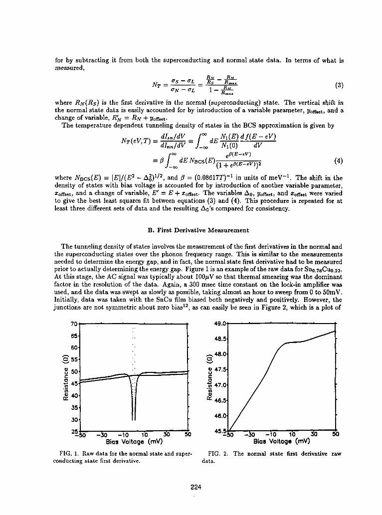
for by subtracting it from both the superconducting and normal state data. In terms of what ismeasured,
NT -- _rS -- O'L -- Rs -- R=.=_N -- trL 1 -- _B_U_ (3)
/_max
where RN(Rs) is the first derivative in the normal (superconducting) state. The vertical shift inthe normal state data is easily accounted for by introduction of a variable parameter, Yoffset,and achange of variable, R_v = RN + Yoffset.
The temperature dependent tunneling density of states in the BCS approximation is given by
dI, n/dY /oo N_(E) d f(E - eY)NT (eV, T) - dInn/dV - .,-co dE N1 (0) "dV
,_ e#(E-eY)
= fl dE NBcs(E)(1 + e_(E-'v))' (4)
where NBcs(E) = [E[/(E 2 - A02)112,and/_ = (0.08617T) -1 in units of meV -z. The shift in thedensity of states with bias voltage is accounted for by introduction of another variable parameter,Zotrset, and a change of variable, E' = E + zofrset. The variables A0, yotrget,and zotrset were variedto give the best least squares fit between equations (3) and (4). This procedure is repeated for atleast three different sets of data and the resulting A0's compared for consistency.
B. First Derivative Measurement
The tunneling density of states involves the measurement of the first derivatives in the normal andthe superconducting states over the phonon frequency range. This is similar to the measurementsneeded to determine the energy gap, and in fact, the normal state first derivative had to be measuredprior to actually determining the energy gap. Figure 1 is an example of the raw data for Sn0.rsCu0.22.At this stage, the AC signal was typically about 100pV so that thermal smearing was the dominantfactor in the resolution of the data. Again, a 300 msec time constant on the lock-in amplifier wasused, and the data was swept as slowly as possible, taking almost an hour to sweep from 0 to 50mV.Initially, data was taken with the SnCu film biased both negatively and positively. However, thejunctions are not symmetric about zero bias 1_, as can easily be seen in Figure 2, which is a plot of
70 , , , , 49.0 ' ' ' '
65' .. 48.560.
48.055,50, 47.s
o
45' ._ 47.0"_ 40. "_€_n. _ 46.5
35,
30 48.0
251 --30 -10 10 30 50 45.5 , -- - - -_0 _ 10 10 :30
Bias Voltage (mY) Bias Voltage (mY)
FIG. 1. Rawdata for the normalstate and super- FIG. 2. The normal state first derivative rawconducting state first derivative, data.
224
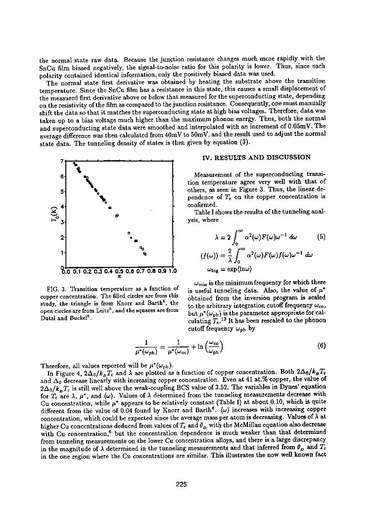
the normal state raw data. Because the junction resistance changes much more rapidly with theSnCu film biased negatively, the signal-to-noise ratio for this polarity is lower. Thus, since eachpolarity contained identical information, only the positively biased data was used.
The normal state first derivative was obtained by heating the substrate above the transitiontemperature. Since the SnCu film has a resistance in this state, this causes a small displacement ofthe measured first derivative above or below that measured for the superconducting state, dependingon the resistivity of the film as compared to the junction resistance. Consequently, one must manuallyshift the data so that it matches the superconducting state at high bias voltages. Therefore, data wastaken up to a bias voltage much higher than the maximum phonon energy. Thus, both the normaland superconducting state data were smoothed and interpolated with an increment of 0.05mV. Theaverage difference was then calculated from 40mV to 50mV, and the result used to adjust the normalstate data. The tunneling density of states is then given by equation (3).
7 _ • . , . . IV. RESULTS AND DISCUSSION%
6 _ Measurement of the superconducting transi-tion temperature agree very well with that of
5 %. others, as seen in Figure 3. Thus, the linear de-_. pendence of Tc on the copperconcentrationis
.-. 4 . confirmed.v TableIshowstheresultsofthetunnelinganal-_o 3 _ ysis,where
° ff2 .. =2 -1 (5)1' q:
(f(w)) = _ c_2(w)F(_v)f(w)w-1 dw
_ 0".10:2 0:3 '0:4 0:5 0:8 0:7 0:8 0:9 1.0 0JIog = exp(lnw)x
Wminis the minimum frequency for which thereFIG. 3. Transition temperature as a function of is useful tunneling data. Also, the value of #*
copper concentration. The filledcircles arefrom this obtained from the inversion program is scaledstudy, the triangle is from Knorr and Barth4, the to the arbitrary integration cutoff frequency Woo,open circles are from Leitz s , and the squares axe from but _* (Wph) is the parameter appropriate for cal-Dutzi and Buckel6. culating To.13It has been rescaled to the phonon
cutoff frequency Wph by
1 I (0:co)p*(Wph)--#*(woo)+ In\OJP h , (6)
Therefore,allvaluesreportedwillbe#*(Wph).InFigure4,2Ao/kBTcand A areplottedasa functionofcopperconcentration.Both2Ao/k_Tc
and A0 decreaselinearlywithincreasingcopperconcentration.Evenat41 at.%copper,thevalueof2A0/k_T_isstillwellabovetheweak-couplingBCS valueof3.52.The variablesinDynes'equationforTc areA,#*,and (w).ValuesofA determinedfromthetunnelingmeasurementsdecreasewithCu concentration,whilep* appearstoberelativelyconstant(TableI)atabout0.10,whichisquitedifferentfromthevalueof0.04foundby Knorrand Barth4. (o_)increaseswithincreasingcopperconcentration,whichcouldbeexpectedsincetheaveragemassperatomisdecreasing.ValuesofA athigherCu concentrationsdeducedfromvaluesofT0and0D withtheMcMillanequationalsodecreasewithCu concentration,6 buttheconcentrationdependenceismuch weakerthanthatdeterminedfromtunnelingmeasurementson thelowerCu concentrationalloys,andthereisa largediscrepancyin the magnitude of A determined in the tunneling measurements and that inferred from 0o and T_in the one region where the Cu concentrations are similar. This illustrates the now well known fact
225
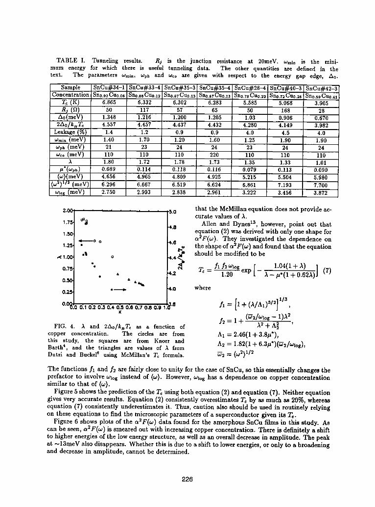
TABLE I. Tunneling results. Rj is the junction resistance at 20meV. _'min is the mini-mum energy for which there is useful tunneling data. The other quantities axe defined in thetext. The parameters OJmin,t_ph and woo are given with respect to the energy gap edge, Ao.
Sample SnCu#34-1 SnCu#33--4 SnCu#35-3 SnCu#35-4 SnCu#28-4 SnCu#40-3 SnCu#42-3Concentration Sno.9_Cuo.o8Sno.ssCuo.12Sno.sTCu0.13Sno.aTCuo.13Sno.TsCuo.22Sno.72Cuo.2sSno.59Cu
Tc (K) 6.865 6.332 6.302 6.283 5.585 5.068 3.905R, (_) 50 117 57 65 5o 168 28
Ao (meV) 1.348 1.216 1.200 1.205 1.03 0.906 0.6702Ao/kBTc 4.557 4.457 4.437 4.432 4.280 4.149 3.982
Leakage(%) 1.4 1.2 0.9 0.9 4.0 4.5 4.0Wmin(meV) 1.40 1.70 1.20 1.60 1.25 1.90 1.90hYph(meV) 21 23 24 24 23 24 24woo(meV) 110 110 110 220 110 110 110
A 1.80 1.72 1.78 1.73 1.35 1.33 1.01_t_*(_4/ph) 0.089 0.114 0.118 0.116 0.079 0.113 0.090
(w)(meV) 4.656 4.965 4.809 4.925 5.215 5.504 5.980{w2)112(meV) 6.296 6.667 6.519 6.624 6.861 7.193 7.700_og (meV) 2.750 2.993 2.838 2.961 3.222 3.456 3.872
2.00 ' 3.0 that the McMillan equation does not provide ac-
1.75" oa_ curate values of _.Allen and Dynes13, however, point out that4.81.50. equation (2) was derived with only one shape for
a2F(w). They investigated the dependence on1.25' ._-----o o 4.6 _u the shape of aSF(w) and found that the equation
,_ 1.00' =_ _ should be modified to beeo o 4..4. ,_
0.7' t"q. Tc .,fl fs O_logexp [ - I_i'_-_) ]• ,, 1.2 1.20 A- # (1 + 0.62)_)J (7)0.50 =
0.25 *"-_ _.0 where
0:1 0_. 0:,3 0:4 0:5 0.6 0.7 0:8 0:,= 1 .8 fl -----[1 + (_/A1) 3/2] 1]3,o.oq
x
fs = 1+ (_2/Wlog - 1)AsFIG. 4. A and 2Ao/kaTc as a function of As+ A2 '
copper concentration. The circles axe from A1 =2.46(1+3.8p*),
this study, the squares axe from Knott and As : 1.82(1+fi.3p*)(_2/Wlog),Baxth4, and the triangles axe values of A fromDutzi and Buckel 6 using McMillan's Tc formula. _2 = (W2)I/2
The functions fl and f2 are fairly close to unity for the case of SnCu, so this essentially changes theprefactor to involve Wlog instead of (w). However, Wloghas a dependence on copper concentrationsimilar to that of (w).
Figure 5 shows the prediction of the Tc using both equation (2) and equation (7). Neither equationgives very accurate results. Equation (2) consistently overestimates Tc by as much as 20%, whereasequation (7) consistently underestimates it. Thus, caution also should be used in routinely relyingon these equations to find the microscopic parameters of a superconductor given its To.
Figure 6 shows plots of the aSF(w) data found for the amorphous SnCu films in this study. Ascan be seen, c_SF(w) is smeared out with increasing copper concentration. There is definitely a shiftto higher energies of the low energy structure, as well as an overall decrease in amplitude. The peakat ,_13meV also disappears. Whether this is due to a shift to lower energies, or only to a broadeningand decrease in amplitude, cannot be determined.
226
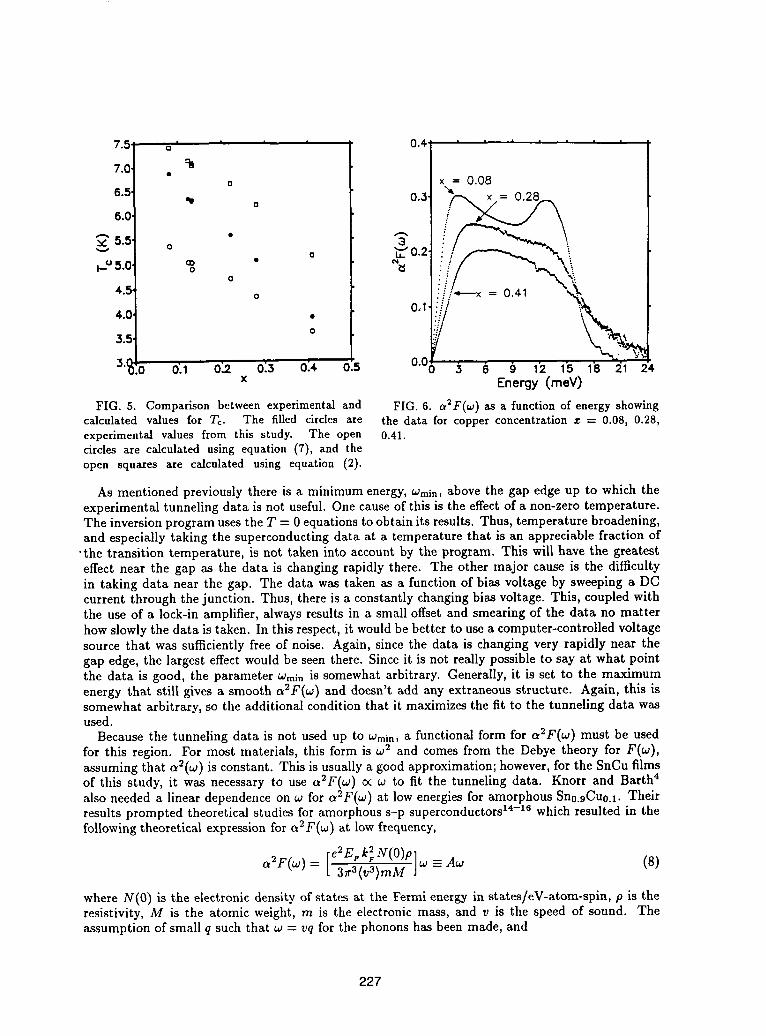
7.5 a ' ' ' ' 0.4 ' ' ' ' ' '
7.0. %a x = 0.08
°° . oo.o, \v 5.5 3
0
__o5.0 _o " _ / ,0
4..5 o
4.0 * 0,1 '" " X:'_o
3.5
3J 0 0".1 0:2 0_3 0_4. 0.5 0"00 3 6 9 12 15 18 21 24x Energy (meV)
FIG. 5. Comparison between experimental and FIG. 6. a2F(w) as a function of energy showingcalculated values for To. The filled circles are the data for copper concentration x = 0.08, 0.28,experimental values from this study. The open 0.41.circles are calculated using equation (7), and theopen squares are calculated using equation (2).
As mentioned previously there is a minimum energy, Wmin,above the gap edge up to which theexperimental tunneling data is not useful. One cause of this is the effect of a non-zero temperature.The inversion program uses the T = 0 equations to obtain its results. Thus, temperature broadening,and especially taking the superconducting data at a temperature that is an appreciable fraction of
•the transition temperature, is not taken into account by the program. This will have the greatesteffect near the gap as the data is changing rapidly there. The other major cause is the difficultyin taking data near the gap. The data was taken as a function of bias voltage by sweeping a DCcurrent through the junction. Thus, there is a constantly changing bias voltage. This, coupled withthe use of a lock-in amplifier, always results in a small offset and smearing of the data no matterhow slowly the data is taken. In this respect, it would be better to use a computer-controlled voltagesource that was sufficiently free of noise. Again, since the data is changing very rapidly near thegap edge, the largest effect would be seen there. Since it is not really possible to say at what pointthe data is good, the parameter Wminis somewhat arbitrary. Generally, it is set to the maximumenergy that still gives a smooth a2F(w) and doesn't add any extraneous structure. Again, this issomewhat arbitrary, so the additional condition that it maximizes the fit to the tunneling data wasused.
Because the tunneling data is not used up to O$min,a functional form for a2F(w) must be usedfor this region. For most materials, this form is w2 and comes from the Debye theory for F(w),assuming that a2(w) is constant. This is usually a good approximation; however, for the SnCu filmsof this study, it was necessary to use a2F(w) oc w to fit the tunneling data. Knorr and Barth 4also needed a linear dependence on w for a2F(w) at low energies for amorphous Sno.9Cuo.1. Theirresults prompted theoretical studies for amorphous s-p superconductors 14-16 which resulted in thefollowing theoretical expression for cx2F(w) at low frequency,
re2EF N(0)pl_2F(w) =[_ jw- Aw (8)
where N(0) is the electronic density of states at the Fermi energy in states/eV-atom-spin, p is theresistivity, M is the atomic weight, m is the electronic mass, and v is the speed of sound. Theassumption of small q such that w = vq for the phonons has been made, and
227
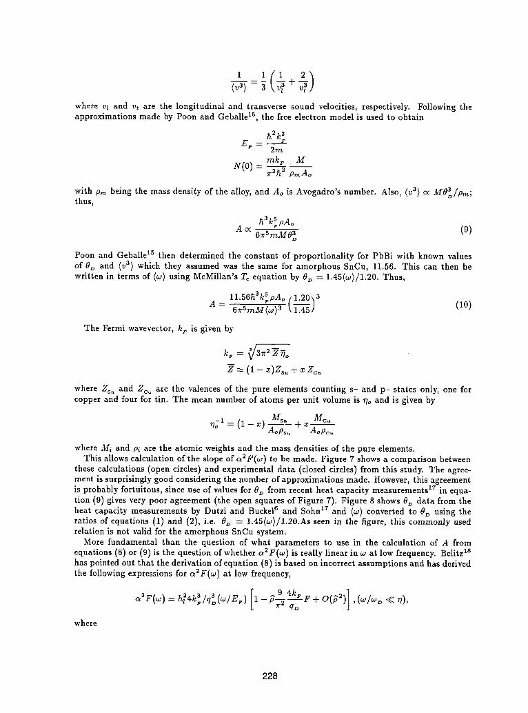
1(v 3) -- 3 +
where vz and vt are the longitudinal and transverse sound velocities, respectively. Following theapproximations made by Poon and Geballe zS, the free electron model is used to obtain
h2]c2F
EF 2m
N(O) = ink. U7r2h2 pmAo
with Pm being the mass density of the alloy, and Ao is Avogadro's number. Also, @3) oc MO3/pm;thus,
A oc h3k_pA°6rrSrnM O3 (9)
Poon and Geballe zs then determined the constant of proportionality for PbBi with known valuesof 0D and (v3) which they assumed was the same for amorphous SnCu, 11.56. This can then bewritten in terms of (co) using McMillan's Tc equation by 0t, = 1.45@)/1.20. Thus,
ll'56hak_pA° ( 1"20"_3 (10)A= 67rSrnM(w) 3 \1.45]
The Fermi wavevector, kt is given by
Z = (1 - x)Zs, + x Zc, ,
where Zs, and Zc, ' are the valences of the pure elements counting s- and p- states only, one forcopper and four for tin. The mean number of atoms per unit volume is _7oand is given by
rlo z = (1 - x) Ms`` Mc"+ XAopc,,
where Mi and Pi are the atomic weights and the mass densities of the pure elements.This allows calculation of the slope of a2F(co) to be made. Figure 7 shows a comparison between
these calculations (open circles) and experimental data (closed circles) from this study. The agree-ment is surprisingly good considering the number of approximations made. However, this agreementis probably fortuitous, since use of values for 0D from recent heat capacity measurements 17 in equa-tion (9) gives very poor agreement (the open squares of Figure 7). Figure 8 shows 0" data from theheat capacity measurements by Dutzi and Buckel 6 and Sohn z7 and (co) converted to 0D using theratios of equations (1) and (2), i.e. 0_, = 1.45(@/1.20.As seen in the figure, this commonly usedrelation is not valid for the amorphous SnCu system.
More fundamental than the question of what parameters to use in the calculation of A fromequations (8) or (9) is the question of whether a2F(co) is really linear in co at low frequency. Belitz zshas pointed out that the derivation of equation (8) is based on incorrect assumptions and has derivedthe following expressions for JF(co) at low frequency,
[ ^9 4k_'F+O('fi2)]'(co/co_<<rl) 'a2F(co) = h_4k3 /q3(co/E_,) 1 - p--fi qD
where
228
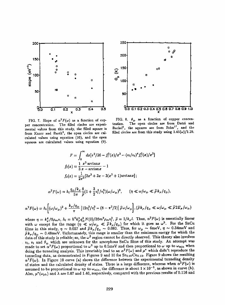
200 .... 250 " , , , ,Q
• 200' o150, • _
_ oL> o ...., 150 oa
o o v%.=1_'_100 • o o
ca.€ • o cZ>Q100.o
50 al • • • •o 50'
r_
Q
(_0 0.1 0:2 0:3 0:4, 0 00100.10:2 0:3 0:4,0:5 0:6 0.7 0:8 0:9 1.0X X
FIG. 7. Slope of a_F(w) as a function of cop- FIG. 8. 0D as a function of copper concen-per concentration. The filled circles are experi- tration. The open 6Jcles axe from Dutzi andmental values from this study, the filled square is Buckel6, the squares axe from Sohn17, and thefrom Knorr and Baxth4, the open circles axe col- filled circlesare from this study using 1.45(w)/1.20.cNated values using equation (10), and the opensquaxes are calculated values using equation (0).
OO
F= d=[,,V36- ST(=)/=- (,,dv,)'.f2(=)l1 z 2arctanz
fl(z) -- 3 z - arctanz - 1
f,(x) = __a [2z3 -I-3x - 3(x2 -I-1)arctanz] ;
3 51,t.)5\lt,,dloj \3 O'}/O'}Dsa'F(w)-hiqv/l%8(l+'_Vtl t)t / o), (il<< <<'PkFIqo),aTr p
a2F( )__h, + [12vi3/v-(8- r2/2)] ,(?l:,,Iq<><</wo <<?2Erl o)4 2 2 2 2
where r/= k4/9pmv, hi = h keqoN(O)/36m praV t , "p= 1/kFl. Thus, c_2F(w) is essentially linearwith w except for the range (7/ << w/w o << "pkF/qo) for which it goes as wa. For the SnCufilms in this study, 17,-, 0.057 and "fikF/qo ,,, 0.080. Thus, for wv ,_ 6meV, r/ ,_ 0.34meV and"_kF/qo ,., 0.48meV. Unfortunately, this range is smaller than the minimum energy for which thedata of this study is reliable; so, the wa region cannot be directly observed. This theory also involvesvt, vt and 8o which are unknown for the amorphous SnCu films of this study. An attempt wasmade to set c_2F(w) proportional to w3 up to 0.5meV and then proportional to w up to 0Jmin whendoing the tunneling analysis. This invariably lead to an a2F(w) and p* which didn't reproduce thetunneling data, as demonstrated in Figures 9 and 10 for Sn0.sTCu0.1a.Figure 9 shows the resultinga2F(w). In Figure 10 curve (a) shows the difference between the experimental tunneling densityof states and the calculated density of states. There is a large difference, whereas when _2F(ca) isassumed to be proportional to w up to Wmin,the difference is about 1x 10⁻⁵, as shown in curve (b).Also, _*(_)ph) and ,_ are 0.07 and 1.46, respectively, compared with the previous results of 0.116 and
229
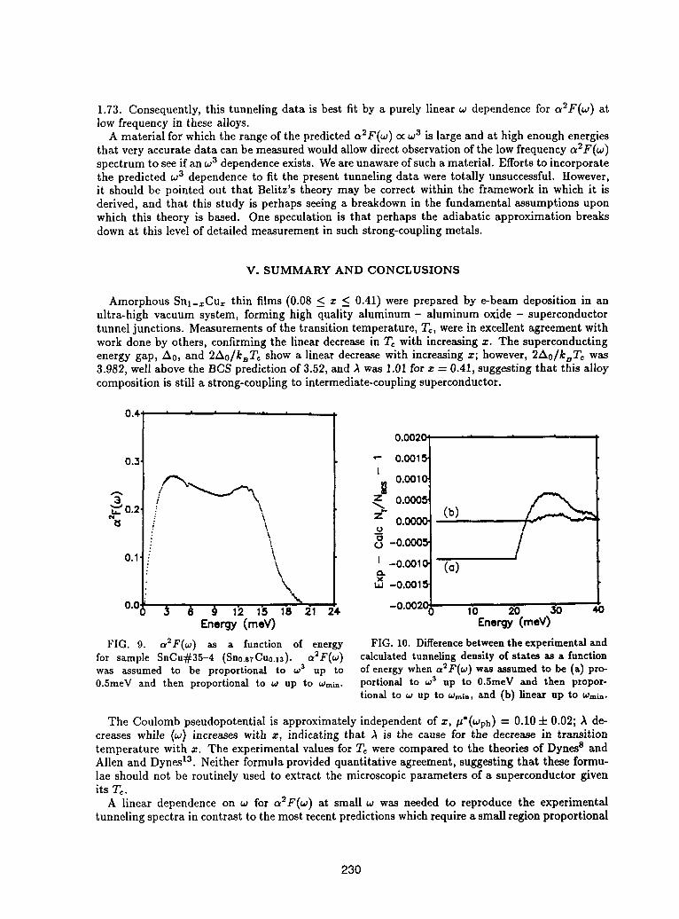
1.73. Consequently, this tunneling data is best fit by a purely linear w dependence for c_2F(w) atlow frequency in these alloys.
A material for which the range of the predicted a_F(w) oc,_3 is large and at high enough energiesthat very accurate data can be measured would allow direct observation of the low frequency a2F(w)spectrum to see if an ,_3 dependence exists. We are unaware of such a material. Efforts to incorporatethe predicted w3 dependence to fit the present tunneling data were totally unsuccessful. However,it should be pointed out that Belitz's theory may be correct within the framework in which it isderived, and that this study is perhaps seeing a breakdown in the fundamental assumptions uponwhich this theory is based. One speculation is that perhaps the adiabatic approximation breaksdown at this level of detailed measurement in such strong-coupling metals.
V. SUMMARY AND CONCLUSIONS
Amorphous Snl_=Cu= thin films (0.08 < z < 0.41) were prepared by e-beam deposition in anultra-high vacuum system, forming high quality aluminum - aluminum oxide - superconductortunnel junctions. Measurements of the transition temperature, To, were in excellent agreement withwork done by others, confirming the linear decrease in Tc with increasing z. The superconductingenergy gap, A0, and 2Ao/k_Tc show a linear decrease with increasing z; however, 2Ao/ksTc was3.982, well above the BCS prediction of 3.52, and A was 1.01 for z = 0.41, suggesting that this alloycomposition is still a strong-coupling to intermediate-coupling superconductor.
0"411_ 0.0020 ' ' '
0.3] i/'_N.,__ ] "- 0.0015
I 0.0010
I0.1_4 I
w
0.0 10 40Energy (meV) Energy(meV)
FIG. 9. tr2F(w) as a function of energy FIG. 10. Differencebetweenthe experimentalandfor sample SnCu#35-4 (Sn0.sTCu0.13). a2F(w) calculatedtunneling density of states as a functionwas assumed to be proportional to w3 up to of energy whenct2F(w)was assumedto be (a) pro-0.5meV and then proportional to _aup to Wmin. portional to w3 up to 0.5meV and then propor-
tional to w up to Wmln,and (b) linear up to taml..
The Coulomb pseudopotential is approximately independent of z, p*(0Jph) --" 0.10 "4-0.02; ._ de-creases while @) increases with z, indicating that ,_ is the cause for the decrease in transitiontemperature with z. The experimental values for T¢ were compared to the theories of Dynes s andAllen and Dynes 13. Neither formula provided quantitative agreement, suggesting that these formu-lae should not be routinely used to extract the microscopic parameters of a superconductor givenits T¢.
A linear dependence on _ for a2F@) at small oJ was needed to reproduce the experimentaltunneling spectra in contrast to the most recent predictions which require a small region proportional
230
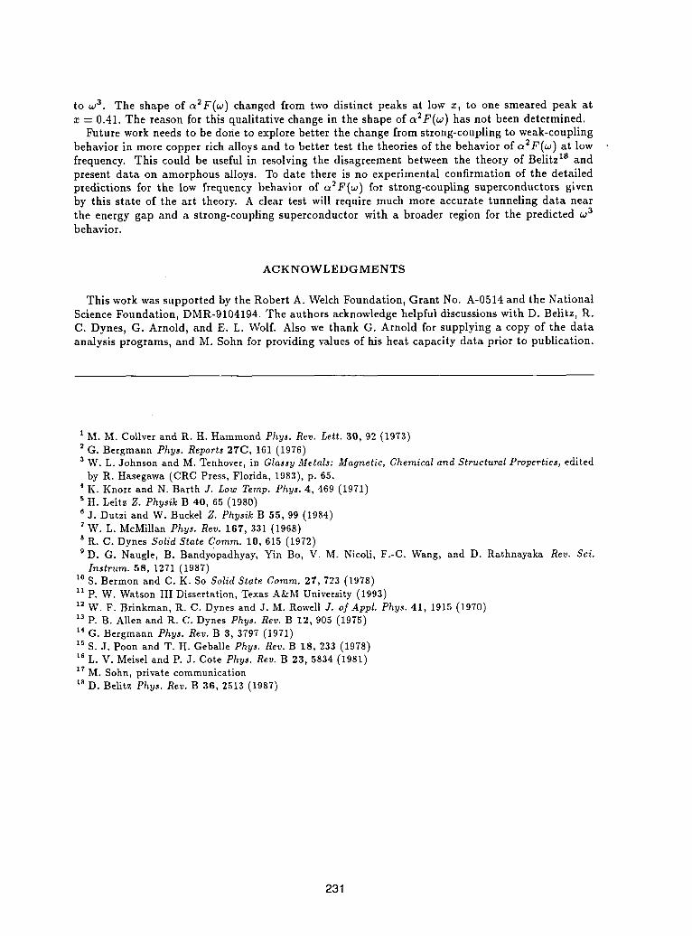
to _o3. The shape of +x2F(oJ) changed from two distinct peaks at low x, to one smeared peak atx = 0.41. The reason for this qualitative change in the shape of c_2F(_0) has not been determined.
Future work needs to be done to explore better the change from strong-coupling to weak-couplingbehavior in more copper rich alloys and to better test the theories of the behavior of c_2F(w) at lowfrequency. This could be useful in resolving the disagreement between the theory of Belitz 18 andpresent data on amorphous alloys. To date there is no experimental confirmation of the detailedpredictions for the low frequency behavior of a2F(w) for strong-coupling superconductors givenby this state of the art theory. A clear test will require much more accurate tunneling data nearthe energy gap and a strong-coupling superconductor with a broader region for the predicted wabehavior.
ACKNOWLEDGMENTS
This work was supported by the Robert A. Welch Foundation, Grant No. A-0514 and the NationalScience Foundation, DMR-9104194. The authors acknowledge helpful discussions with D. Belitz, R.C. Dynes, G. Arnold, and E. L. Wolf. Also we thank G. Arnold for supplying a copy of the dataanalysis programs, and M. Sohn for providing values of his heat capacity data prior to publication.
1 M. M. Coltver and R. H. Hammond Phys. Rev. Left. 30, 92 (1973)2 G. Bergmann Phys. Reports 27C, 161 (1976)3 W. L. Johnson and M. Tenhover, in Glassy Metals: Magnetic, Chemical and Structural Properties, edited
by R. Hasegawa (CRC Press, Florida, 1983), p. 65.4 K. Knorr and N. Barth J. Low Temp. Phys. 4, 469 (1971)s H. Leitz Z. Physik B 40, 65 (1980)6 j. Dutzi and W. Buekel Z. Physik B 55, 99 (1984)r W. L. McMillan Phys. Rev. 167, 331 (1968)s R. C. Dynes Solid State Comm. 10, 615 (1972)9 D. G. Naugle, B. Bandyopadhyay, Yin Bo, V. M. Nieoli, F.-C. Wang, and D. Rathnayaka Rev. Sci.
Instrum. 58, 1271 (1987)10S. Bermon and C. K. So Solid State Comm. 27, 723 (1978)11p. W. Watson III Dissertation, Texas A&M University (1993)12 W. F. Brinkman, R. C. Dynes and J. M. Rowell J. of Appl. Phys. 41, 1915 (1970)13 p. B. Allen and R. C. Dynes Phys. Rev. B 12,905 (1975)14G. Bergmann Phys. Rev. B 3, 3797 (1971)15S. J. Poon and T. H. Geballe Phys. Rev. B 18,233 (1978)16L. V. Meisel and P. J. Cote Phys. Rev. B 23, 5834 (1981)lr M. Sohn, private communication
is D. Belitz Phys. Rev. B 36, 2513 (1987)
231
CHANGES IN THE SUPERCONDUCTING PROPERTIES OF HIGH-Tc CERAMICSPRODUCED BY APPLIED ELECTRIC FIELDS.
B.I.Smirnov,T.S.Orlova,H.-J.KaufmannA.F.Ioffe Physico-Technical Institute, Russian Academy of Sciences,St.Petersburg 194(}21,Russia
AbstractEffect of an electrostatic field in the electrode- insulator-superconductor system on the current-voltage characteristics ofhigh-Tc ceramics with various composition and different preparationtechnology }]asbeen studied at.77K. Ceramics of Y-Ba-Cu-O (123) andBi-Pb-Sr-Ca-Cu-O (2223) systems and also ones doped by Ag havebee,]used. Electric field strength has been up to 14()MV/m.It.]]asbee,] shown that there are reversible changes in the criticalcurrent Ic and in the conductivity in electric field at thecurrents somewhat more than Ic at T<Tc, while at T>Tc the notice-able electric field effect has not bee,] found. These effects arequalitatively similar in both ceramic systems. High negative andpositive gate voltages result, in an increase of the conductivity.The electric field effect, is modified by magnetic field H. Thefield effect decreases wit}] increasing magnetic field anddisappears at H>30 Oe° In Y-Ba-Cu-O/Ag (10 wt.%) ceramics the fieldeffect,is practically absent.It.may be supposed that in the ceramics the field-induced effect isconsistent wit.}]weak links at grain boundaries.
I.IntroductionProblem of an electric field effect, on the conductivity of
superconductors has attracted attention for more than 3(1 years[I-3]. The first experimental paper [I] reported that indium andtin films d_70_ thick subjected to fields E=30 MV/m exhibited achange in the conductivity and a shift in critical temperature Tc
by ATc_I0-4K.After the discovery of high-Tc superconductors similar studies
were stimulated, especially during last four years [4-9]. In mostcases thin films were objects of these investigations because it isusually believed that the field effect is attributed to a change ofthe carrier concentration in very thin surface layer of about 5_thickness [6]. Considerable modulation of Tc and thecurrent-voltage characteristics under applied electric field werereported [7-9].
At the same time there are dat_ on the electric field effect inquite thick low-Tc superconductors° The 0.6K shift in Tc for
Ba(PbBi)()3 single crystals of (1.6ironthickness was reported in [I0].In the case of high-To superconductors the field effect can occuralso in less perfect samples of quite large thickness [II-14].
In the present paper we demonstrate the experimental evidencefor considerable reversible effect of an applied electric field onthe conductivity of high-To ceramics.
The following questions will be presented and discussed inthe paper :
I° Reversible effect,of an applied electric field onthecurrent-voltage characteristics of high-To ceramics at T<Tc.
2° Influence of the electric field polarity on the effect.3. The electric field effect in the presence of magnetic field.
232
4. Influence of silver addition to the ceramics on the effect.
2.Exper imentaiMain results have been obtained on yttrium ceramics of the 123
system° Some tests ]]avebeen made on similar ceramics doped bysilver and also on Bi-based compound of the 2223 system.
Samples of l+'ectangularshape were prepared by standard powdersintering method and had dimensions of about 1.5x2x4 ms. By varyingthe anneal temperature and time, and the rate of the cooling, it
• -t t"was possible to obtain _Bao[.u3.)7 x (YBCO) ceramics with varioussuperconducting transition properties, the value of Tc remainingalmost the same (9()K_TcS93K)but the critical current density jc
O 9varying much more (lA/cm_<_c<i+10A/cm_') [15].
To obtain samples containing silver, the finished pure
YBa2[.u3' t"37_x(x_0.07) pellets were again crushed, and silver powderwas added. Samples of this mixture were compacted and then twiceannealed in oxygen at 930°C for 6 h, with crushing and compactingbetween the anneals° To verify the effect,of silver on the ceramicproperties, control samples were also prepared, and treated likethe others except that no silver was added.
Investigations of field-induced effect were carried out in themetal- insulator- superconductor system shown in Fig.l. Teflon filmof thickness 1=5(|pm was used as the insulator. Such a configura-tion allows us to apply considerable positive (or negative) gatevoltage U up to 7 kV between the gate electrode and a superconduc-tor.
Current-voltage (I-V) characteristics were taken with astandard four-probe technique, and Ic, the experimental criticalcurrent, was determined by a i pV/mm criterion.
It should be noted that the leakage current in the electrode-insulator-superconductor system did not exceed [4nA at the maximumvoltage U=TkV, whereas the transport current could reach a fewamperes.
We studied effect,of an electric field on the I-V characteris-tics of the ceramics. The experiment was carried out in thefollowing way. At first I-V curve without electric field wasmeasured° Then at some chosen point of this curve (Io-Vo) a gatevoltage O was applied and drain-source voltage c_nge (AV=V-Vo) ata constant transport current was deter_tined. Electric field (E=UiI)can be c_ed smoothly from 0 to 140 MV/m or some electric fieldEo was switched s_rply on or off. The similar measurements were._de for Various drain-source voltages Vo, i.e. for different tran-sport currents. Also it was possible to measure and compare valuesof Ic and I-V c_racteristics without and with an electric field[16,17]. In addition, all the above mentioned experiments could beperformed in a _b_gneticfield H generated by an energized coil anddirected parallel to the electric field [17].
3.Results and discussionIn the superconducting state, the I-V characteristics can be
significantly affected by the gate voltage U (see Fig.2). Strongelectric field shifts the I-V curve to the right, i.e. enhances thecritical current and reduces the sample resistance R at I>Ic nomatter what the polarity of the field.
Figo3 shows change of drain-source voltage due to the switchingof strong electric field on and off at 77 K. It,is seen that vol-
233
tage decreases at the moment when the field is switched on. Theopposite effect is observed when the field is switched off.Strangely enough, we obtained qualitatively similar result also inthe case when a metal foil 15 _m thick was placed between theinsulator and a supe[-eonducting sample [18].
Thus, we can conclude'that in the ce_amic samples at tempera-ture below Tc the field effect also exists. The value of drain-source voltage is restored after removing the field, i.e. the fieldeffect,has reversible character.
The following Fig. 4 demonstrates characteristic experimentaldependence drain-source voltage versus electric field for the casesof positive and negative gate voltages at 77K. As seen, the charac-ter of this relationship V(E) ca,]depend on the field polarity.Applying a positive gate voltage to a fresh sample usually resultsin decrease of V (AV<0). In the case of a negative gate voltage thevalue of V first rises with E (AV>0) but then gradually decreaseshaving a maximum at electric field E_40 t_¢/m. After the electricfield has reached E_-_0-70MV/m the value of AV c_nges its sign sothat we _ve an decrease of the resistance. It is of interest thatafter the prolonged testing a sample the relationships V(E) canchange essentially, including the appearance of maximum on thecurve V(E) also for a positive gate voltage [19].
A qualitatively similar result was obtained for high Tc ceramic
Bi[.85Pb0.35Sr[.gCa2.[Cu3.[Oy (Tc_SK) [16].It should be also noted that in the above both cases the elec-
tric field effect,exists only at T<Tc. At T>Tc the noticeable fieldeffect was not observed [16].
Our further interest was in the elucidation of the electricfield effect peculiarities arising from the application of amagnetic field. Fig.5 shows the influence of strong electric fieldE=-120 MV/m on the ]-V characteristics of YBCO ceramic in variousmagnetic fields H. It is seen that the shift of the I-V curvesunder an electric field depends on the value of H. So, at H=0 thefield effect is sufficiently large (AR/R=AV/V can reach 100% forlow V and about 40% for high V). However, it falls off withincreasing H and practically disappears at H->30Oe.
Fig.6 presents the results on the influence of an electric anda magnetic fields on the critical current. At H=0, the criticalcurrent [c is seen to grow with increasing E (see inset of Fig.6),the change reaching"Alc/Ic_10% at E=-120 MVim. After the magneticfield is switched on, the electric field effect,falls off rapidly,to practically disappear at H£3(} Oe. Thus, the electric fieldeffect on the I-V curves is Observed only at low magnetic fields.
Next we will consider the field effect in YBa2CU3OT_ x /Ag(i0 wt.%) ceramics (YBCO/Ag). Fig.7 displays the comparison of theexperimental results obtained for the pure YBCO and YBCO/Ag ceramicsamples. As seen doping with silver suppresses the field effectpractica lly complete ly,
Thus, the results obtained show that an applied electric fieldaffects the current-voltage characteristics of high-Tc ceramics atT<Tc and can modify the value of the critical current ]c. The fieldeffect is reversible. It should be stressed that the field effectobserved in high-Tc ceramics is qualitatively different from theeffect in the high-Tc films.
The question of what is the possible mechanism behind theobserved field effect,arises. Unfortunately, the nature of this
234
effect has not bee,] clear for us. It may be only supposed that inthe ceramics the field-induced effect is consistent with change ofweak link states at.grain boundaries [16]. This is supported inpsrt,icular by those facts that.both magnetic field and doping withsilver greatly suppress the electric field effect,° In the lattercsse the a_rked reduction of t,he field effect ca,] be explainedreplacing the weak links of superconductor- insulator- superconductortype (S/I/S) by the weak links of superconductor-normal metal-superconductor type (S/N/S) [20]o Further studies are required togain a better understanding of the nature of the field effectobserved.
4.ConclusionsIn summary, the present, study allows the following conclusions:I. An applied electric field affects the I-V characteristics of
high Tc ceramics at T<Tc and ca]]modify the value of the criticalcurrent Ic.
2. In ceramic samples at T>Tc the noticeable field-inducedeffect was not found.
3. The effect }]asreversible character. Strong positive andnegative gate voltages lead to enhancement of the conductivity.
4. Magnetic field and adding silver to the ceramics result inthe suppression of the electric field effect.
5. It may be supposed that,in ceramics the field-induced effectis consistent with weak links at grain boundaries.
235
ReferencesI. Glover R.E. and Sherrill M.D. Phys. Rev. Lett. 5, 248 (1960)2. Sandomirskii V.B. Pis'ma Zh. Exp. Teor. Fiz. 2, [496(1965)3. Meissner H. Phys. Rev. 154, 422 (1967)4. Hannhart.J., Bednorz J.G., M_illerK.A. and Schlom D.G. Z. Phys. B
83, 307 (1991)5. Mannhart J., Schlom D.G., Bednorz J.G., and M[_ller K.A. Phys.
Rev. Lett. 67, 2099 (1991)6. Xi X.X. , Doughty C, Walkenhorst A. , ]:,wonC., bi Q. and
Venkatesan T. Phys. Rev. Left. 69, 1240 (1992)7. Mannhart.J. Modern Phys. Left. B 6, 555 (1992)8. Xi X.X. and Venkatesan T. Phys. News in 1992, Ed. Schewe P.F:,
American Inst..of Phys. 44 (199:4)9. Lemanov V.V. and Kholkin A.L. Fiz. Tverd. Tela 36, 1537 (1994)10.Bogatko V.V. and Venevzev Yu.N. Fiz. Tverd. Tela 29, 2872 (1987)ll.Gomenyuk Yu.V., Lozovskii V.Z., Lysenko V.S., Pokhodnya K.N.,
Snitko O.V., Syt.enkoT.N. and Tyagul'skii I.P. Dokl. Akad. NaukUkr.SSR, set. A, )_ 11, 49 (1989)
12.Gomenyuk Yu.V., Klyui N.I., Lozovskii V.Z., Lysenko V.S.,Prokof'ev A.Yu., Romanyuk B.N., Syt.enkoT.N. and Tyagul'skii I.P.Sverkhprovodimost': Fizika, Khimija, Tekhnika 4, 762 (1991)
13.Smirnov B.I., Krisht0opov S.V. and Orlova T.S. Fiz. Tverd. Tela34, 2482 (1992)
14.Le,k%novV.V., Kholkin A.L. and Sherman A.B. Pis'ma Zh. Eksp.Teor.Fiz. 56, 58(|(1992)
15.Orlova T.S., Smirnov B.I., Shpeizman V.V., Stepanov Yu. P. andChernova S.P. Fiz. Tverd. Tela 32, 1031 (1990)
16.Smirnov B.I., Orlova T.S. and Krishtopov S.V. Fiz. Tverd. Tela35, 2250 (1993)
17.Smirnov B.I., Orlova T.S. and Kudymov A.N. Fla. Tverd. Tela36, 1529 (1994)
18.Smirnov B.I., Orlova T.S. and Kaufmann H.-J. Fiz. Tverd. Tela36, 460, (1994)
19.Orlova T.S., Smirnov B.I. Supercond. Sci. Technol.(to bepublished)
20.Jung J., Isaac I. and Mohamed M.A-K. Phys. Rev. B 48, 7526(1993)
236
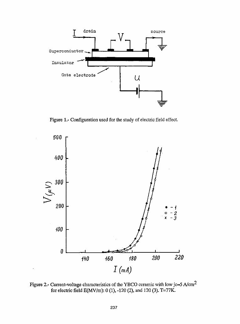
Insulator
Gate electrode (_
=l =2w"
Figure 1.- Configurationused for the study of electric field effect.
if00
z/oo
300-
200 - , -2o
x 3
¢00 -
0 t _ I I
"lqO _60 t80 2.00 220
IFigure 2.- Current-voltagecharacteristicsof the YBCO ceramic with lowjc_5 A/cm 2
for electric field E(MV/m): 0 (1), -120 (2), and 120 (3). T=77K.
237
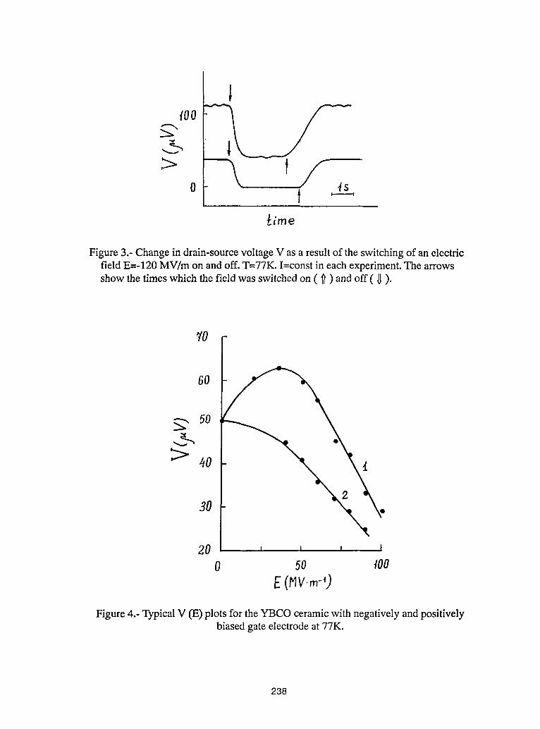
Figure 3.- Change in drain-source voltage V as a result of the switching of an electricfield E=-120 MV/m on and off. T=?7K. I=const in each experiment. The arrowsshow the times which thefield was switched on (/_ ) and off ( _ ).
6O
50
4o
3O
20 , , , I
0 50 tOOE(rV.m-9
Figure 4.- TypicalV (E) plots for theYBCO ceramic with negatively and positivelybiased gate electrode at 77K.
238
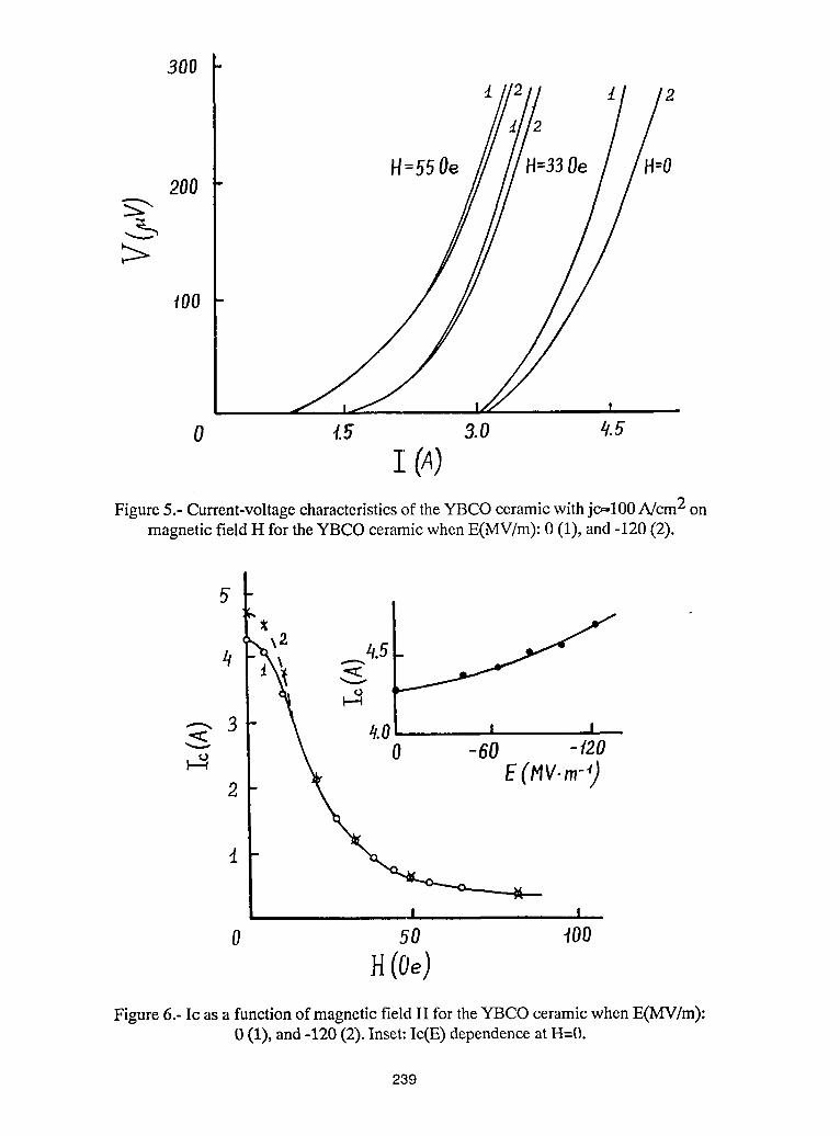
300
,1 t _fl=2H=55 Oe H=33Oe 0200
t00
! I
0 _._ 3.0 0.5
I(A)Figure 5.- Current-voltage characteristics of the YBCO ceramic with jc_100 A/cm 2 on
magnetic field H for the YBCO ceramic when E(MV/m): 0 (1), and -120 (2).
I
0 50 400
Figure 6.- Ic as a function of magnetic field H for theYBCO ceramic when E(MV/m):0 (1), and -120 (2).Inset: Ic(E) dependenceat H=0.
239
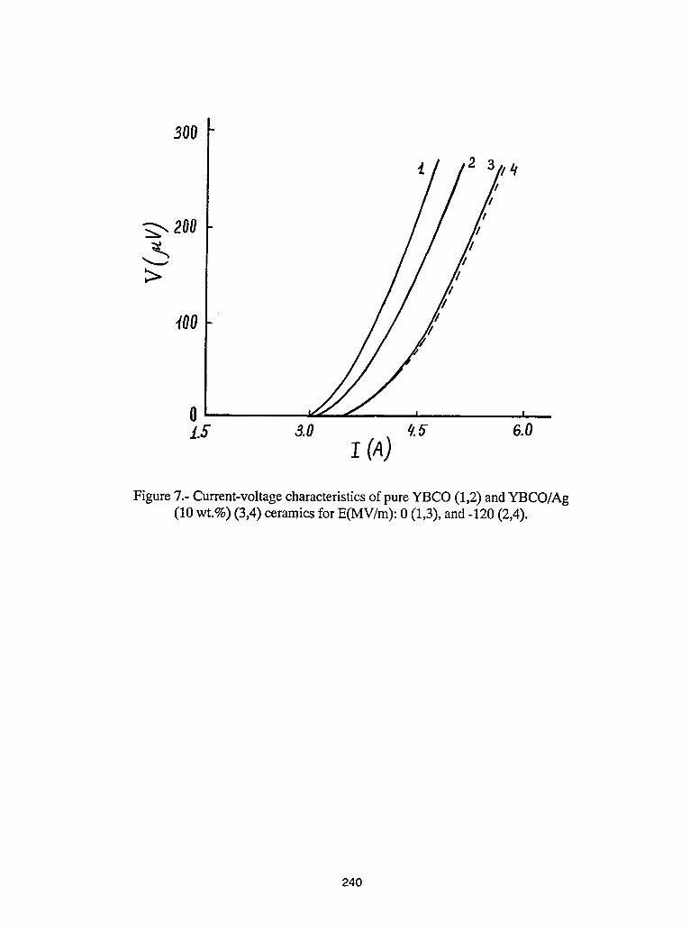
3O0r
2OO
:>
Figure 7.- Current-voltagecharacteristicsof pure YBCO (1,2) and YBCO/Ag(10 wt.%) (3,4) ceramics for E(MV/M):0 (1,3), and -120 (2,4).
240
EFFECT OF Nb205 AND V205 ADDITION ON THE
SUPERCONDUCTING PROPERTIES OF YBazCuO Y THIN FILMS
S.SRINIVAS AND A.K.BHATNAGAR
SCHOOL OF PHYSICS,UNIV.OF HYDERABAD,HYDERABAD 500134, INDIA
AND
R.PINTO, S.P.PAI, P.R.APTE, S.C.PURANDARE AND C.P.D.SOUZA
SOLID STATE ELECTRONICS GROUP, T.I.F.R., BOMBAY, INDIA
ABSTRACT
The effect of Nb O and V O addition on the25 25
superconducting properties and microstructure of YBa2Cu30 hasYbeen studied in thin films. Polycrystalline targets for laser
ablation were prepared by mixing high purity V205 or Nb205 powders
with a well characterized YBa2Cu3Oy powder in the range 0 to 4 wt_by solid state reaction method. Thin films (_1500 A thickness) of
the above targets were grown on <100> SrTiO 3 (STO) and <100>
LaA103 (LAO) substrates at 700°C temperature by Pulsed Laser
Deposition (PLD) technique. In the case of Nb205 addition we havenoticed an increase in J upto 0.5 wt% and higher additiveo
concentration (greater than 0.5 wt%) have degraded the
superconducting properties. However, in the case of V205addition, there is an improvement in current density and
microstructural properties up to I wt% and the superconducting
properties degrade for concentrations greater than 1 wt%. The
best Jc for 0.5 wt_ of Nb205 added YBCO thin film is 1.6x10⁶ A/cm2
and for that of V205 added sample is 3.4xi06 A/cm2 at 77K as
compared to the pure YBa2Cu3Oy (YBCO) film Jc (1"2xi06 A/cm2)
observed on STO substates. The reason for improvement in Jc and
microstruetural properties in the case of V205 addition could be
due to the low melting of V205 (690°C) which can act as a verygood surfaetant during deposition. Over all, we have realized
that Nb205 addition or V205 addition to YBCO have shown
significant improvement over the undoped YBa2Cu307_ x films grownunder identical conditions
241
1.INTRODUCTION
Research in high temperature superconductivity (HTSC)
has made significant progress towards improving the
microstructural and crystallographic quality of thin films during
the last four years [I-3]. Effect of addition or substitution of
transition metal elements in YBCO compound has been investigated
and it is well established that superconducting properties will be
suppressed by substitution at the Copper site by elements like AI,
Ag, V, Nb, Ta and more severely suppressed by the substitution of
Fe, Co, Ni & Zn [4,5,9]. Also, addition of transition metal
elements to YBCO has resulted in similar effects above a certain
concentration of additive [6]. Evidences confirm that Nb205addition upto 0.5% has resulted in improvement of mechanical,
microstructural and superconducting properties of YBCO compound in
bulk form [7-8]. It has been stated that Silver plays an
important role in improving the microstructural and transport
properties [I0-II] due to dissociation of Ag20 on the substrateand the increased mobility of AE atoms segregating out of the YBCO
grains is responsible for the enlargement and alignment of grains
in Ag-doped YBCO films. This result has motivated us to study the
doping of some oxides which can melt on the substrate at low
temperatures to aid the grain growth. In the present study we
report the addition effect of V205 and Nb205 to YBCO on itssuperconducting properties.
2.EXPERIMENTAL
Targets for the Laser deposition were prepared by mixing
3N pure V205 and Nb205 powders with a well characterized YBa2Cu3Oy(YBCO, 99.99% pure) in the concentration range of 0.0 to 4 wt% by
solid state reaction method. Thin films of above samples were
made using an excimer laser ( Lambda Physik 301:KrF,248 nm and
300mm focal length quartz lens for laser beam focussing) [12].
The substrate to target distance was 4.5cm and growth pressure was
242
200 mTorr oxygen at 700°C substrate temperature and films were
deposited in the thickness range 1500-2000 Angstroms. Structural
characterization was done using JEOL 8030 XRD powder
diffractometer and surface morphology of the films were studied by
JEOL 840 scanning electron microscopy (SEM). DC electrical
resistivity was measured by using standard linear four probe
technique. Critical current density measurements were carried out
using laser patterned 40-20 _m wide and Imm long microbridg_s. The
standard voltage criterion of l_V/mm was used for determining JC"
3. RESULTS AND DISCUSSION
a) V205 DOPED YBCO THIN FILMS :
XRD data has shown c-axis oriented films for 0.5 to 1
wt% V205 added YBCO thin films. An addition 4 wt% of V205 hasyielded poor quality superconducting thin films (fig. 3) compared
to undoped YBCO thin film. Undoped YBCO thin film made under
identical conditions has relatively lower Tc (_89K) and Jc
(_l.2xl06A/cm 2 at 77K ) values. The best results for V205 dopedYBCO thin films were observed for 0.5 wt% addition ( T _ 89.5K¢,O
and J _ 3.6xl06A/cm 2 at 77K). Such high Jc values in the case ofc
undoped YBCO thin films could be realized, only at higher
deposition temparatures ( 800°C) on STO<I00> substrate [9]. The
V205 doped YBCO thin films deposited on LAO substrate have yieldedrelatively inferior quality superconducting flims when compared to
that deposited on SiTiO 3 <I00> substrate. The reason for this
could be a good lattice match of SiTiO 3 with YBCO. We couldn'tget any information from scanning electron micrographs as they
are featureless which may be due to perfect orientation of grains.
It is evident from fig. 3, the slope of the Tc-T vs _r-Jc plot of
V205 doped films is larger compared to that of undoped YBCO film,indicating grain enlargement and reduction of weak links.
b) Nb205 DOPED YBCO THIN FILMS :
Our results show that Nb O addition upto 0.5 wt% inz5
243
bulk has improved the superconducting properties of YBCO compound,
however, no substantial improvement in the case of thin films
deposited even on SrTiOg<100> substrates has been noticed. X-raydiffraction patterns have showed (fig. I) that films are c- axis
oriented YBCO along with growth of <hoo> oriented a secondary
phase YBazNbO6 with the increase of Nb205 _ lwt%. However, the Tc89 I and J = I 6 x 10⁶ A/cm2 for Nb = 0 5 wt% doped YBCO thinc
films have been recorded, degradation of superconducting
properties has been noticed with increase in Nb O concentration (25£ lwt% ). The slope of T - T vs _r-j plot is slightly largerc c
than the undoped YBCO film but smaller than V205 doped YBCO thinfilm which indicates that the grain size has not substantially
improved when compared with that of V205 added film.
c) POSSIBLE EXPLANATION :
From the above results it is clear that V205 additionhas improved the quality of YBCO superconducting thin films
compared to that of Nb205 added YBCO thin films on SrTiO 3
substrata. Films deposited on LaAIO 3 substrates have resulted inpoor quality due to the lattice mismatch between substrate and
film. However, there is an improvement in Jc of 0.5 wt _ V205
added film compared to that of Nb20s added and undoped YBCO film.
Due to its low melting point, V205 during growth process may actas a surfactant and aids in better coalition of the individual
grain which leads to increase in grain size of YBCO, where as in
the case of Nb205 addition since the melting point is very highsuch a process does not take place• This is clearly evidenced in
the improvement in J in the former case• De Gennes [13] andc
Clarke [14] have predicted a mechanism that near T the criticalc
current density of S-N-S junctions can be expressed as
Jc(T) _ (Tc -T)2 exp (-d/In)
Where d is the thickness of the the grain boundary layer
and [niS the coherence length• From this equation the nature ofgrain boundaries in doped and undoped YBCO thin films can be
studied by plotting Tc-T vs _-Jc and the slope of this plot will
244
decide the grain boundary domain thickness which in turn reflects
on the nature of weak links. We have plotted T -T vs ]/--J valueso c
upto 77K for the sake of comparison in the cases of 0.5 wt % added
V205 and Nb205 and undoped YBCO film. From fig.2, it is evident
that V205 addition yields a larger slope value compared to Nb205doped and undoped YBCO thin films, which is indicative of
improvement in grain structure.
CONCLUSIONS
The effect of V O and Nb O addition on the25 25
superconducting properties of YBCO thin films is studied. It has
been realized that V O can act as a very good surfactant thanz 5Nb O because of its low melting point. Also, it is found that2 5
there is an improvement in the Jc of the 0.5 wt% V205 doped YBCO
thin film compared to that of Nb205 (0.5 wt %) doped and undopedYBCO thin films. This could be due to the surfactant effect of
V O which melts at relatively low temperature and improves the2 5
grain structure. On the other hand, the addition of NbzO5 (whichhas high melting point) does not show such improvement.
ACKNOWLEDGEMENTS:
One of the authors (SS) would like to thank University
Grants Commission, INDIA for financial support and (A.K.B) is
thankful to Council of Scientific and Industrial Research (CSIR)
for HTSC research support .
REFERENCES:
1. J. Z. Sun, M. J. Scharen, L.C. Bourne. J.R Schrieffer :
Phys. Rev. 8.44(1991) 5275.
2. B. Roas, L. Schultz, G. Saemann and Ischenko : Phys. Rev.
Lett. 64(1990) 479.
3. S.Tahara S.M.Anlage, J. Halbritten, C.B.Eom, D.K. Fork,
T.H.Geballe and M.R. Beasley : Phys. Rev. B 41(1990) 11203.
4. Y.Maeno T. Tomita M.Kyogoku, S.Awaji, Y.A. Oki, K.Hoshimo,
A. Mimanit,T. Fujita,: Nature328(1987) 512.
5. G.Xiao, M.Z.Leeplak, A.Gavnm, F.H.Steitz, A.Bakshai and C.L.
245
Chein Phys. Rev. Lett.60(1988) 1446.
6. C.W. Kammlott, T.H. Tiefel and S.Jin, Appl. Phys. Lett
56(1990) 2459.
7. ¥asuo Hikichi, T.Maruta S.Suziki, M.Miyamoto, S.Okada and
K.Kudou. Jpn. J. Appl. Phys. 31(1992) L1232.
8. K.V.Paulouse, J.Koshy, A.D.Damodaran Jpn. J. of App.
Phys.31(1992) L1232.
9. V.P.N Padmanabhan and K.Shahi Physica C 208(1993) 263.
I0. R.Pinto et.al, Physica C 207(1993) 13.
II. D.Kumar et.al, Appl.Phys.Lett.62(1993) 3572.
12. R.Pinto et.al, Physica C 196(1992) 264.
13. P.G.DeGennes, Rev Mod Phys 36(1964) 225.
14. J. Clarke, Proe R.Soc. London A 308(1969) 447.
246
D O P A N T CON CENTRATION
Fig .1 . Dopant c o n c . vs. Tc p l o t s f o r (d) V205 dopod Y BCO thin film (b) NbZOs d o p e d Y B C O thin f i lm
Fig.2. vs ( T c - T I h p \ o t s , f o r undopod , V205 d o p o d a n d NbZO5 dopod Y B C O f i lms grown at 7 0 0 ° C on SrT$13 < l o o >
( 1 V 2 0 5 d o p e d f i lm ( b) N b2O5 doped f i Im ( c ) Undoped f l lm
-
I I I I I 1
r
5 15 25 35 45 55
2 8 ANGLE
5 15 25 35 45 55
2 8 ANGLE
(ii)
Fig. 3. Xrd Patterns of ( i ) V2 O5 (i i ) Nb201 added Y BCO
Thin films.
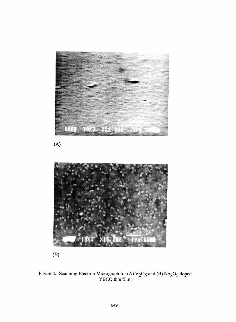
(A)
(B)
Figure 4.- Scanning Electron Micrograph for (A) V205 and (B) Nb205 dopedYBCO thinfilm.
249
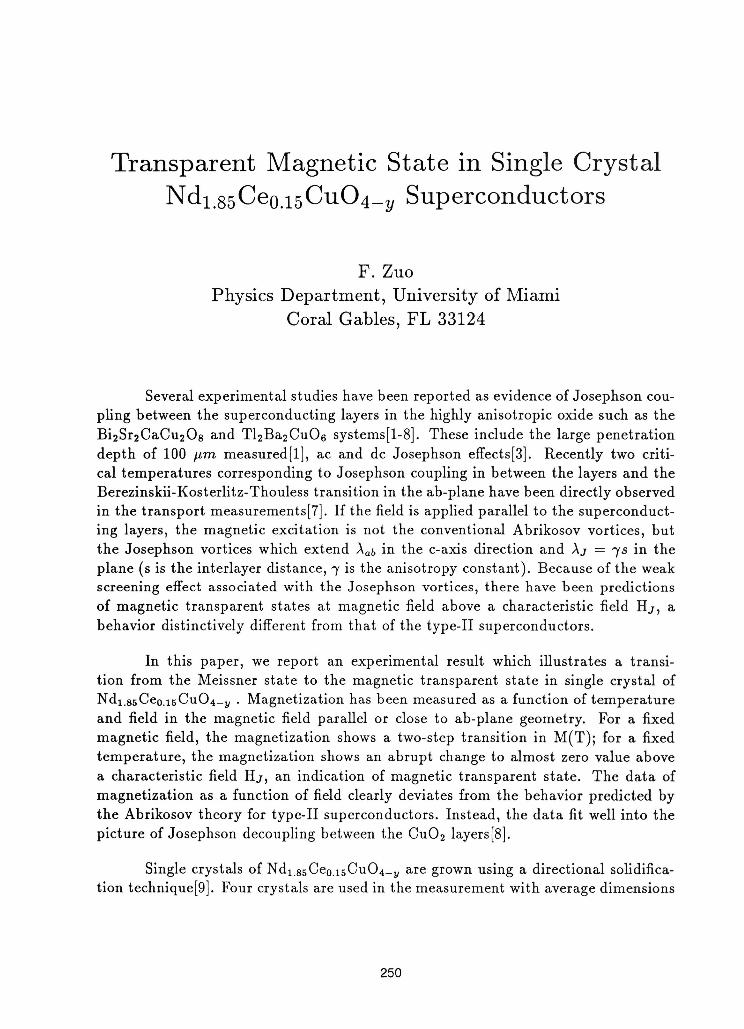
Transparent Magnetic State in Single CrystalNd1.ssCe0.15CuO4-y Superconductors
F. Zuo
Physics Department, University of MiamiCorm Gables, FL 33124
Several experimental studies have been reported as evidence of Josephson cou-pling between the superconducting layers in the highly anisotropic oxide such as theBi2Sr2CaCu_Os and T12Ba2CuO6 systems[i-8]. These include the large penetrationdepth of 100 /zm measured[l], ac and dc Josephson effects[3]. Recently two criti-cal temperatures corresponding to Josephson coupling in between the layers and theBerezinskii-Kosterlitz-Thouless transition in the ab-plane have been directly observedin the transport measurements[7]. If the field is applied parallel to the superconduct-ing layers, the magnetic excitation is not the conventional Abrikosov vortices, butthe Josephson vortices which extend Aabin the c-axis direction and A3 = 7s in theplane (s is the interlayer distance, 3' is the anisotropy constant). Because of the weakscreening effect associated with the Josephson vortices, there have been predictionsof magnetic transparent states at magnetic field above a characteristic field I-Ij, abehavior distinctively different from that of the type-II superconductors.
In this paper, we report an experimental result which illustrates a transi-tion from the Meissner state to the magnetic transparent state in single crystal ofNdl.ssCe0.15CuO4-u • Magnetization has been measured as a function of temperatureand field in the magnetic field parallel or close to ab-plane geometry. For a fixedmagnetic field, the magnetization shows a two-step transition in M(T); for a fixedtemperature, the magnetization shows an abrupt change to almost zero value abovea characteristic field H j, an indication of magnetic transparent state. The data ofmagnetization as a function of field clearly deviates from the behavior predicted bythe Abrikosov theory for type-II superconductors. Instead, the data fit well into thepicture of Josephson decoupling between the CuO2 layers[8].
Single crystals of Ndl.ssCe0.1_CuO4_y are grown using a directional solidifica-tion technique[9]. Four crystals are used in the measurement with average dimensions
250
of 1x 1× 0.02mm. Extensive measurements were made on two samples A and B withTc of 22.5K and 21K, respectively. Typical magnetic transition widths measuredat 1G with zero-field cooling are about 1-2K. Measurements are performed using aQuantum Design magnetometer with low field options. After degaussing and magnetresetting (quenching) the remanent field is typically 5-10raG. All measurements weredone with the sample zero-field cooled to a temperature below To. Magnetizations inboth directions H 11ab and HI ab were measured. For samples with ab-plane alignedparallel to the field, mlsalignment of a few degrees were often observed.
Shown in Figure l(a) and (b) are plots of magnetization of sample A asa function of temperature in field parallel to c-axls and ab-plane, respectively. InFigure l(a), the transition temperature Tc is about 22.5K and M(T) is almost fiatfor T below 20K. The transition width is less than 2K in the applied field of 1G,an indication of high crystal quality. The magnetization in the field close to ab-plane direction is clearly different from that of field parallel to c-axis direction. Foran applied field of 10G, there are two apparent transitions. The high temperaturetransition corresponds to the same Tc as from Figure l(a), the lower transition startsaround 12K and magnetization saturates above 16K.
0 ' ' ' _ T,__
i -1 H--1G \\C zfe /_o -2 (a)
--5 I I I I I
5 10 15 20 25
I I I I I
0.0 H=IO G H\\ ab zfc
7o-0.5_,..,-1.0
I I I I I
5 10 15 20 25
T(K)
Fig. 1 Temperature dependence ofmagnetization in field parallel to c-axis (a) and ab-plane (b).
Shown in Figure 2 is an overlay of magnetization as a function of tempera-ture of sample A at different applied field H=30G, 40G, 50G and 60G. Again, two
25!
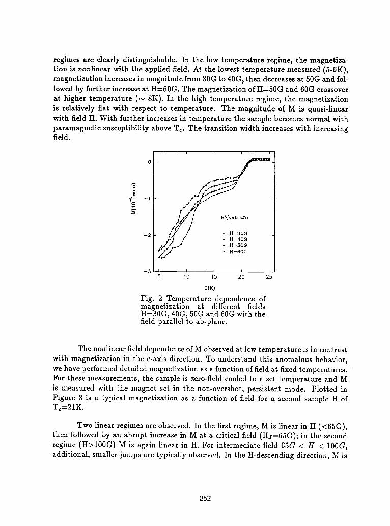
regimes are dearly distinguishable. In the low temperature regime, the magnetiza-tion is nonlinear with the applied field. At the lowest temperature measured (5-6K),magnetization increases in magnitude from 30G to 40G, then decreases at 50G and fol-lowed by further increase at H=60G. The magnetization of H=50G and 60G crossoverat higher temperature (,-_ 8K). In the high temperature regime, the magnetizationis relatively flat with respect to temperature. The magnitude of M is quasi-linearwith field H. With further increases in temperature the sample becomes normal withparamagnetic susceptibility above To. The transition width increases with increasingfield.
I I I I I
0
-2 l,f t . H=3OG// / • H=4OG
-3 i i i n t5 10 15 20 25
T(K)
Fig. 2 Temperature dependence ofmagnetization at different fieldsH=30G, 40G, 50G and 60G with thefield parallel to ab-plane.
The nonlinear field dependence of M observed at low temperature is in contrastwith magnetization in the c-axis direction. To understand this anomalous behavior,we have performed detailed magnetization as a function of field at fixed temperatures.For these measurements, the sample is zero-field cooled to a set temperature and Mis measured with the magnet set in the non-overshot, persistent mode. Plotted inFigure 3 is a typical magnetization as a function of field for a second sample B ofTc=21K.
Two linear regimes are observed. In the first regime, M is linear in H (<65G),then followed by an abrupt increase in M at a critical field (H.r=fSG); in the secondregime (H>100G) M is again linear in H. For intermediate field 65G < H < 100G,additional, smaller jumps are typically observed. In the H-descending direction, M is
252
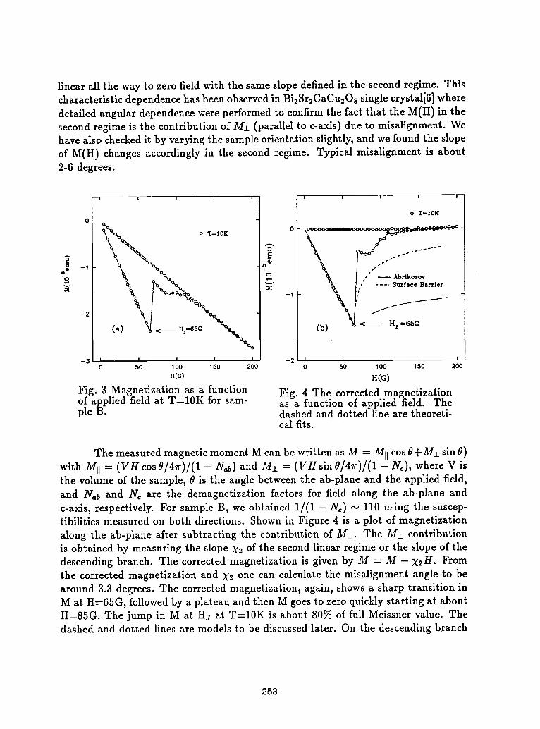
linear all the way to zero field with the same slope defined in the second regime. Thischaracteristic dependence has been observed in Bi2Sr2CaCu20s single crystal[61 wheredetailed angular dependence were performed to confirm the fact that the M(H) in thesecond regime is the contribution of M± (parallel to c-axis) due to mlsalignment. Wehave also checked it by varying the sample orientation slightly, and we found the slope
of M(H) changes accordingly in the second regime. Typical n_salignment is about2-6 degrees.
I I I I I I I I I I
o T-IOK0
o T=IOK 0
°
-2 _ -1
(a) H,=aSG (b)
--3 I I I I --2 I I I I I
O 50 1O0 150 200 0 50 1O0 150 200
H(G) H(G)
Fig. 3 Magnetization as a function Fig. 4 The corrected magnetizationof applied field at T=10K for sam- as a function of applied field. Theple B. dashed and dotted line are theoreti-
cal fits.
The measured magnetic moment M can be written as M = 3/11cos O+M_Lsin O)with MII = (VII cos0/4rr)/(1 - Nab) and M± = (VII sin 0/4or)/(1 - Arc),where V isthe volume of the sample, 8 is the angle between the ab-plane and the applied field,and Nab and Arcare the demagnetization factors for field along the ab-plane andc-axis, respectively. For sample B, we obtained 1/(1 - Arc) ,,_ 110 using the suscep-tibilities measured on both directions. Shown in Figure 4 is a plot of magnetizationalong the ab-plane after subtracting the contribution of M±. The M± contributionis obtained by measuring the slope X, of the second linear regime or the slope of thedescending branch. The corrected magnetization is given by M = M - X2II. Fromthe corrected magnetization and X2 one can calculate the misalignment angle to bearound 3.3 degrees. The corrected magnetization, again, shows a sharp transition inM at H=65G, followedby a plateau and then M goes to zero quickly starting at aboutH=85G. The jump in M at Hj at T=10K is about 80% of full Meissner value. Thedashed and dotted lines are models to be discussed later. On the descending branch
253
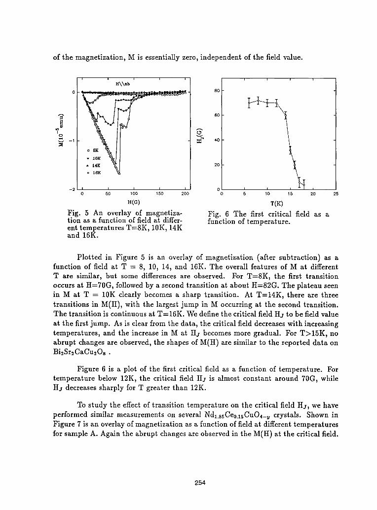
of the magnetization, M is essentially zero, independent of the field value.
i I I I I I I I I
x\\ab800
3 0o h
• lox NI I 201[] 16K "t_ \
f-T-2, , , , , 0 , o ; '00 50 100 150 200 0 5 1 1 2 25
H(G) T(K)
Fig. 5 An overlay of magnetiza- Fig. 6 The first critical field as ation as a function of field at differ- function of temperature.ent temperatures T=8K, 10K, 14Kand 16K.
Plotted in Figure 5 is an overlay of magnetization (after subtraction) as afunction of field at T = 8, 10, 14, and 16K. The overall features of M at differentT are similar, but some differences are observed. For T=8K, the first transitionoccurs at H=70G, followed by a second transition at about H=82G. The plateau seenin M at T = 10K clearly becomes a sharp transition. At T=14K, there are threetransitions in M(H), with the largest jump in M occurring at the second transition.The transition is continuous at T=16K. We define the critical field Ha to be field valueat the first jump. As is clear from the data, the critical field decreases with increasingtemperatures, and the increase in M at Hj becomes more gradual. For T>15K, noabrupt changes are observed, the shapes of M(H) are similar to the reported data onBi2SrzCaCu2Os .
Figure 6 is a plot of the first critical field as a function of temperature. Fortemperature below 12K, the critical field Hj is almost constant around 70G, whileHa decreases sharply for T greater than 12K.
To study the effect of transition temperature on the critical field Ha, we have
performed similar measurements on several Ndl.ssCe0.1_CuO4-v crystals. Shown inFigure 7 is an overlay of magnetization as a function of field at different temperaturesfor sample A. Again the abrupt changes are observed in the M(H) at the critical field.
254
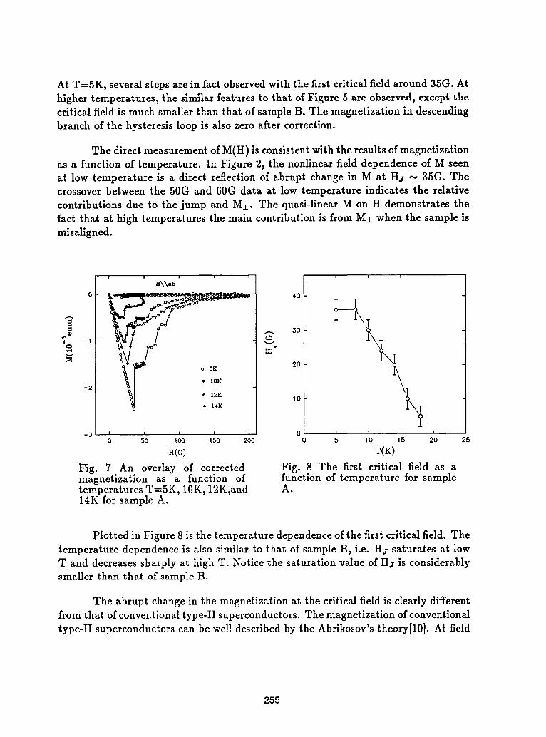
At T=5K, several steps are in fact observed with the first critical field around 35G. Athigher temperatures, the similar features to that of Figure 5 are observed, except thecritical field is much smaller than that of sample B. The magnetization in descendingbranch of the hysteresis loop is also zero after correction.
The direct measurement of M(H) is consistent with the results of magnetizationas a function of temperature. In Figure 2, the nonlinear field dependence of M seenat low temperature is a direct reflection of abrupt change in M at Hj _ 35G. Thecrossover between the 50G and 60G data at low temperature indicates the relativecontributions due to the jump and M±. The quasi-linear M on H demonstrates thefact that at high temperatures the main contribution is from M± when the sample ismisaligned.
' ' H\\ab .... ' = '
o 40
20
\T
,= I2K I 10 "_\= I4K /
, i o I I I I--3 i i I i i0 50 100 150 200 5 10 15 20 25
H(G) T(K)
Fig. ? An overlay of corrected Fig. 8 The first critical field as amagnetization as a function of function of temperature for sampletemperatures T=SK, 10K, 12K,and A.14K for sample A.
Plotted in Figure 8 is the temperature dependence of the first critical field. Thetemperature dependence is also similar to that of sample B, i.e. Ha saturates at lowT and decreases sharply at high T. Notice the saturation value of Hj is considerablysmaller than that of sample B.
The abrupt change in the magnetization at the critical field is clearly differentfrom that of conventional type-II superconductors. The magnetization of conventionaltype-II superconductors can be well described by the Abrikosov's theory[10]. At field
255
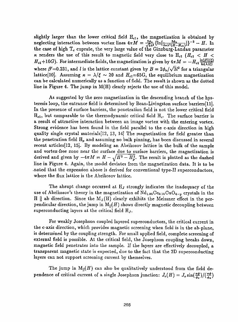
slightly larger than the lower critical field Hcz, the magnetization is obtained by
neglecting interaction between vortex lines 4_rM = _{ln[4._2_L_,_)]} -2 - H. Inthe case of high Tc cuprate, the very large value of the Ginzburg-Landau parameteri¢ renders the use of this result to magnetic field very close to He1 (Hcz < H <
He1+10G). For intermediate fields, the magnetization is given by 4_'M = ---cl a_(x/Owhere/3'=0.231, and l is the lattice constant given by B = 2dpo/v/3l2 for a triangularlattice[10]. Assuming _€= _/_ _-,20 and Hcl=65G, the equilibrium magnetizationcan be calculated numerically as a function of field. The result is shown as the dottedline in Figure 4. The jump in M(H) clearly rejects the use of this model.
As suggested by the zero magnetization in the descending branch of the hys-teresis loop, the entrance field is determined by Bean-Livingston surface barriers[11].In the presence of surface barriers, the penetration field is not the lower critical fieldHCz,but comparable to the thermodynamic critical field He. The surface barrier isa result of attractive interaction between an image vortex with the entering vortex.Strong evidence has been found in the field parallel to the c-axis direction in highquality single crystal materials[12, 13, 14] The magnetization for field greater thanthe penetration field Hv and assuming no bulk pinning, has been discussed in severalrecent articles[12, 15]. By modeling an Abrikosov lattice in the bulk of the sampleand vortex-free zone near the surface due to surface barriers, the magnetization is
derived and given by -4_'M = H - _/H 2- Hi. The result is plotted as the dashedline in Figure 4. Again, the model deviates from the magnetization data. It is to be.noted that the expression above is derived for conventional type-II superconductors,where the flux lattice is the Abrikosov lattice.
The abrupt change occurred at Hj strongly indicates the inadequacy of theuse of Abrikosov's theory in the magnetization of Ndl.ssCe0.zsCuO4__ crystals in theH [I ab direction. Since the M±(H) clearly exhibits the Meissner effect in the per-pendicular direction, the jump in MII(H) shows directly magnetic decoupling betweensuperconducting layers at the critical field Hj.
For weakly Josephson coupled layered superconductors, the critical current inthe c-axis direction, which provides magnetic screening when field is in the ab-plane,is determined by the coupling strength. For small applied field, complete screening ofexternal field is possible. At the critical field, the Josephson coupling breaks down,magnetic field penetrates into the sample. If the layers are effectively decoupled, atransparent magnetic state is expected, due to the fact that the 2D superconductinglayers can not support screening current by themselves.
The jump in MII(H) can also be qualitatively understood from the field de-
pendence of critical current of a single Josephson junction: J_(H) = dosin(_)/(_)
256
where J_(H) is the field dependent critical current, Jo is the maximum zero fieldcritical current, and € is the magnetic flux through the junction. The critical currentis almost zero when there is a finite number of Josephson vortices threading throughthe junction. Assume the magnetization is proportional to the critical current, Mshould become zero as Josephson vortices penetrate into the junction. For stackedlayers with Josephson coupling, the field dependence of Jc should not be the same asthat of single Josephson junction, rather one expects a stronger reduction in Jc(H)with increasing H. In this picture, the experimentally observed smaller jumps in themagnetization data thus would indicate the presence of superconducting layers withdifferent Josephson couplings.
To describe the vortex state of the Josephson coupled superconducting stacksquantitatively, one has to solve the coupled Lawrence-Doniach equations[16]. In thecase where the applied field is tilted to the superconducting layers, several theoreticalmodels are proposed. Recently it has been shown that there are two distinct vortexstructures depending on the anisotropy constant 7 = .kj/s, where Aj is the Josephsonpenetration depth and s is the separation between the superconducting layers. If,kj < Aab,the theory suggests a tilted vortex line structure, where different segmentsof vortex lines parallel to the ab-planes are connected by pancakes residing in the ab-planes[17, 18]. If Aj > Aab,the model predicts that coexisting sets of perpendicularand parallel vortices should exist when the field is applied dose to the ab-plane. TheAbrikosov vortices are due to Ha_,and Josephson vortices are due to HII. The vorticesdue to HII and Ha_act independently of each other. The complete Meissner effect is
possible only if HII < H_ and Ha_ < H_. For HII > H_, HII penetrates into thelayers between the CuO2 planes almost completely, creating the so called magnetictransparent state[18, 19, 20].
The experimental results clearly demonstrate the complete Meissner state forH < Hj. The linear field dependence of M in the descending branch and the overlap-ping M(H) at high field indicate H± < H_. For H > Hj, there are only Josephsonvortices parallel to the ab-plane and M± is still in the Meissner state. The jumpin M(H) for H > Hj indicates the transition to the magnetic transparent state inJosephson coupled layered superconductors.
The difference in magnetic transition around the critical field between the
Nd1.ssCe0.15CuO4-u and the Bi2Sr_CaCu2Os , TI_Ba2CuO6 crystals is not dear. Onepossibility is that the Bi_Sr2CaCu_Os , T12Ba2Cu06 crystals studied are very thick[6,21]. A broad distribution in the coupling strength will smear out the transition. Thispicture is supported by a recent report which shows a similar abrupt change in M(H)in another TI_Ba2CuOs crystal[22].
In summary, we have presented an experimental measurement of an abrupt
257
Josephson decoupling between the Cu02 planes at the critical field Hj parallel toab-planes. The abrupt increase in M(H) at Hj is incompatible with the conventionalAbrikosov theory. For field Hi[ > H j, the magnetic field has a complete penetra-tion in between the superconducting layers-a magnetic transparent state. A moredetailed study of H.r as a function of Tc will help to elucidate the mechanism ofsuperconductivity in the layered superconductors.
References
[1] J. R. Cooper, L. Forro, and B. Keszei, Nature (London) 343,444 (1990).
[2] J. C. Martinez et al. Phys. Rev. Left. 69, 2276 (1992).
[3] R. Kleiner, F. Steinmyer, G. Kunkel, and P. Muller, Phys. Rev. Left. 68, 2394(1992).
[4] R. Fastampa, M. Giura, R. Marcon, and E. Silva, Phys. Rev. Left. 67, 1795(1992).
[5] A. Schilling, R. Jin, J. D. Guo, and H. R. Oft, Phys. Rev. Left. 71, 1899 (1993).
[6] N. Nakamura, G. D. Gu, and N. Koshizuka, Phys. Rev. Left. 71,915 (1993).
[7] Y. M. Wan, S. E. Hebboul, D. C. Harris, and J. C. Garland, Phys. Rev. Left. 71,157 (1993).
[8] F. Zuo, S. Khizroev, Xiuguang Jiang, J. L. Peng and R. L. Greene, Phys. Rev.Left. 72, 1746 (1994).
[9] J. L. Peng, Z. Y. Li, and R. L. Greene, Physica C, 177, 79 (1991).
[10] P. G. de Gennes, Superconductivity of Metals and Alloys (Benjamin, New York,1966).
[11] C. P. Bean and J. D. Livingston, Phys. Rev. Left. 12, 14 (1964).
[12] L. Burlachkov, Y. Yeshurun, M. Konczykowski, and F. Holtzberg, Phys. Rev.B 45, 8193 (1992); L. Burlachkov, Phys. Rev. B 47, 8056 (1993).
[13] Ming xu et al. Phys. Rev. B 48, 10630 (1993).
[14] F. Zuo, S. Khizroev, Xiuguang Jiang, J. L. Peng and R. L. Greene, Phys. Rev.B 49, 12326 (1994).
258
[15] J. R. Clem, Proc. of Low Temp. Phys.-LT 13, ed. Timmerhaus et al. (Plenum,NY, 1974), Vol.3, P.102.
[16] W. Lawrence and S. Doniach, in Proceedings of Twelfth International Conferenceon Low Temperature Physics, edited by Eizo Kanda (Acedemi, Kyoto, 1971),P.361.
[17] D. Feinberg, and C. ViUard, Phys. Rev. Left. 65,919 (1990).
[18] L. N. Bulaevskii, Soy. Phys. JETP 37, 1133, 1973; and L. N. Bulaevskii, M. Led-vii, and V. G. Kogan, Phys. Re,,'. B 46, 366 (1992); L. N. Bulaevskii andJ. R. Clem, Phys. Re,,'. B 44, 10234 (1991).
[19] P. H. Kes, J. Aarts, V. M. Vinokur, C. J. van der Beek, Phys. Rev. Left. 64,1063(1990).
[20] S. Theodorakis, Phys. Rev. S 42, 10172 (1990).
[21] F. Zuo, S. Khizroev, S. Voss and A. M. Hermann, Phys. Rev. B 49, 9252 (1994).
[22] N. E. Hussey, A. Carrington, J. R. Copper and D. C. Sinclair (to be published).
259
Processing and Property Evaluation of Metal MatrixSuperconducting Materials
Appajosula S. Rao
Naval SurfaceWarfareCenterAnnaplois,MD 21402
ABSTRACT
Metal- superconductor(YBCO)systemshavebeenpreparedand characterizedby resistivity,acsusceptibilityanddc SQUIDmagneticmoment measurements.The silvercompositesshowedsuperconductingtransitionfor all the compositesprocessedandthe superconductingtransitiontemperaturetends to dependuponthe concentrationofthe silverin the composite.Aluminum compositesshowedan unusualresistivityresultswithtwotransitionsaround90K and 120K. The superconductingpropertyof silvercompositescanbe explained qualitatively in terms ofthe proximitytheorythat hasbeensuggestedfor the low temperaturesuperconductors.
KeyWords: Processing,superconductivity,silver, aluminum/ YBCOcomposites
INTRODUCTION
Thepresentdaytechnologyof superconductingelectricalsystemsrequires cryogenicsystemsthat are operationalat liquidheliumtemperatures(temperature_ 4 K). The newgenerationof ceramicsuperconductorsthat can superconductat liquidnitrogentemperatures(temperature- 77 K) offerapotential and logisticaladvantageforboth the systemreliabilityandoperationalcost. Although, fewsuperconductingcomponentsystemsthat can operateat liquidnitrogentemperaturesweredemonstrated,the full potentialof these materialshasnotbeenexploitedto date. This is essentiallydueto the fact thatthe materialsarevery hard brittleanddifficultto form intonet shapedcomponents.In the openliterature,manyattemptswerereportedto improvethe ductilityofthe high temperaturesuperconductingmaterialsbycompostingthem withsilveror gold [1-2]. However,the phenomenologyofthe superconductivityinthe metal - superconductorcompositesystemhasyetto be established.This projectwasundertakenin anattemptto developa processingmethodologyforproducingflexiblesuperconductingwires/ tapeswithdifferentmetallicspeciesand to modelthe mechanismof the superconductivityofthese compositesystems. In this paper,the experimentalresultsobtainedon0 - 72 wt.%silveror aluminumcompositesanda possiblemodelto explainthe superconductingbehaviorof the compositesis beingpresented.
EXPERIMENTAL PROCEDURE
The basicsuperconductingceramicpowder,YBa2Cu306+x,waspreparedby solidstatechemicalreactionand the detailsof thepowdersynthesisweregivenelsewhere[3]. AlthoughpureYBa2Cu306+x powderhasgoodsuperconductingproperties,wefoundthat the presenceof excesscopperoxidewill improvethe finalcompositeproperties.. Therefore,duringthe synthesisofthesuperconductingYBa2Cu306+x powder,nearly5 molesofexcesscopperoxidewereaddedto theprecursors. It shouldbe pointedoutthat any referencein thispaperfor YBa2Cu306+x representtheYBCOwith 5 molesof excessCuO. Fromthe microstructuralcharacterizationand chemicalcompositionalanalysis,it wasfoundthat the excess(5 moles)copperoxideremainedunreactedwith the
26O
finalYBa2Cu306+x compound.However,a smallamountof theexcessCuOwasreducedto metalliccopper.
Theas-synthesizedYBa2Cu306+x powderandcommercialsilveroraluminumpowderweremixedthoroughlyin drystateina ballmillusingzirconiaballs foronehour.Thepowdermixture(silveroraluminumpowderandYBa2Cu306+x powder)wasdrypressedintosmall2.5cmdiameterdiscsunderan appliedpressureof 25,000psi. Thecoldpresseddiscswereplacedbetweentwothicksilveroraluminumplatesandweresinteredat880°C(in the caseof silver)and at400°C(in the caseofaluminum)for30 minutes.Duringsinteringthe compositesamplewasalsosubjectedto a constantaxialloadof 10,000psi.The sintereddiscswerecooledinnitrogenandwerecutintosmall2 X 2 X 25 mmbars.
Themicrostructureofall sampleswas examinedunderbothoptical,scanningandtransmissionelectronmicroscopes.ThestructuralcharacterizationofthesuperconductingYBa2Cu306+x particleswascarriedoutusingx-raydiffraction.The electricalresistanceof all sampleswas measuredas a functionoftemperatureusingadc fourproberesistivitymeasurementunit,ac susceptibilityapparatusand dcSQUIDmagnetometer.
RESULTS
The as-synthesizedYBa2Cu306+x powder hasan averageparticlesize of_ 10microns. Themorphologyof the particlesresemblethat of smallpebblesor rocks.Thedensityof the powderwasfoundto be - 6.0 gmcm'-LUponsintering the YBa2Cu306+x particlestendto sinterto formlong elongatedrodsor plates. The sinteredsamplesshowa zeroresistance(superconducting)transitionanddiamagneticmagneticmoment around86+4 K and hasa crystalstructurethat representsthe orthorhombicstructureof YBa2Cu306+x and the detailedanalysisofthe resultsare givenelsewhere[4-6].
Silver/YBa2Cu306+x CompositeSystem
Figure I showstypicalelectricalresistanceversustemperatureplotsof puresilverandsilver/YBa2Cu306+x composites.The zeroresistancetemperatureversussilverconcentrationin thecompositeswas determinedfroma numberofresistanceversustemperatureplots similarto thoseshownin Figure1 and the resultsare shownin Table1. The resultsindicatethat the silvercompositesshowsuperconductingbehaviorthroughoutthe entireconcentrationrangeinvestigated(0 - 72 wt.%silver).However,the zeroresistancetemperature(Tc) tendsto decreasewithan increasein the concentrationofsilverin the range 0 - 10wt.%and40 - 72 wt.%. The Tc remainsnearlyindependentof silverconcentrationin the range 10-40 wt.%.In addition,the resultsalsosuggestthat the normalstateresistanceofthe compositesdecreaseswithan increasein the silverconcentration.
The typicalmicrostructureof silvercompositesobtainedfrompolishedsamplesurfacesis shownas a functionof silverconcentrationin Figure2. Theresultssuggestthat the distributionofYBa2Cu306+x in silvermatrixis veryuniformandthe degreeofuniformityincreaseswith an increaseinthe concentrationof silverin the composites.In orderto modelthe superconductingpropertyof thecompositesin termsof the separationdistancebetweentwoYBa2Cu306+xparticles,a numberofopticalphotomicrographsrepresentingthe microstructureof all compositeswereobtained.Fromthe micrographs the averageparticlesizewasestimatedand the resultsare givenin Table 1. Assumingthat theparticlesare spherical, andare not connectedin a 3 dimensionalnetwork,the YBa2Cu306+x particle-particleseparationdistancewasestimatedas a functionof silverconcentrationand the resultsare alsoshownin Table 1. The resultssuggest that the particlesizeofYBa2Cu306+x increaseswith anincreasein the silverconcentrationinitiallyin the range0 - 10wt.%. For the silverconcentrationabove10wt.%this trend is reversed.The resultsalso indicatethat the separationdistanceincreaseswith anincreasein the silverconcentration.
261
2 i I I _ I I I I
A B/28"" C DiO,- 24X
E 20
'- E F
"12
"_ 8
4
3 0 7 0 110 15 0 190
Temperature (K)
Figure 1. Electrical resistance versus temperature profiles of commercial silver / YBa2Cu306+ xcomposites. Silver concentration (A) 100, (B) 10, (C) 20, (D) 30, (E) 40, (F) 50, (G) 60 and (H) 63.6wt.%. The actual applied current 20 milli amp.
Table 1. The superconducting transition temperature (Tc), the normal state resistance measured at100 K (R100K), the average YBa2Cu306+ x particle size and the particle - particle separationdistance measured for sintered silver / YBa2Cu306+ x composites as a function of silverconcentration of the composite.
Silver cone. Tc (K) R1001¢ particle size separation distance(wt. %) (ohm _'10-5 (micron) (micron)
0 86 + 4 2000 35 + 42 88 + 4 800 35 + 4 0.25 90 + 2 300 40 + 4 0.5
10 82 + 2 30 45 + 4 1.020 80 + 2 25 40 + 4 4.030 80 + 2 16 37 + 4 8.040 82 + 2 12 25 _+2 15.050 76 + 2 6 23 + 2 22.055 70 + 2 4 20 + 2 26.060 68 + 2 3 18 + 2 30.063.6 62 + 2 2 16 + 2 32.072.2 62 + 2 1 14 + 2 37.0
262
t
Figure 2. Typical micro structure of polished silver / YBa2Cu306+ x composites. Silverconcentration (A) 10, (B) 20, (C) 30, (1)) 40, (E) 50 _ 60 (G) 63.6 and (H) 72 wt.%.
263
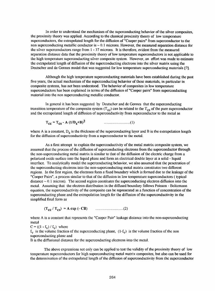
In order to understand the mechanism of the superconducting behavior of the silver composites, the proximity theory was applied. According to the classical proximity theory of low temperature superconductors, the extrapolated length for the diffusion of "Cooper pairs" from superconductor to the non superconducting metallic conductor is - 0.1 microns. However, the measured separation distance for the silver superconductors range from 1 - 37 microns. It is therefore, evident from the measured separation distance data that the proximity theory of low temperature superconductors is not applicable to the high temperature superconducting silver composite system. However, an effort was made to estimate the extrapolated length of difhsion of the superconducting electrons into the silver matrix using the Deutscher and de Gennes model that was suggested for low temperature superconducting materials [7].
Although the high temperature superconducting materials have been established during the past five years, the actual mechanism of the superconducting behavior of these materials, in particular in composite systems, has not been understood. The behavior of composites in low temperature superconductors has been explained in terms of the diffusion of "Cooper pairs" from superconducting material into the non superconducting metallic conductor.
In general it has been suggested by Deutscher and de Gennes that the superconducting transition temperature of the composite system (Tee) can be related to the Tcs of the pure superconductor and the extrapolated length of diffusion of superconductivity from superconductor to the metal as
where A is a constant, Ds is the thickness of the superconducting layer and B is the extrapolation length for the diffusion of superconductivity from a superconductor to the metal.
As a first attempt to explain the superconductivity of the metal matrix composite system, we assumed that the process of the difision of superconducting electrons from the superconductor through the non-superconducting metal matrix is similar to that of the diffusion of the electric charge from a polarized oxide surface into the liquid phase and form an electrical double layer at a solid - liquid interface. To analpcally model the superconducting behavior, we also assumed that the penetration of the superconducting electrons into the non-superconducting metal matrix constitutes two different regions. In the first region, the electrons form a fixed boundary which is formed due to the leakage of the "Cooper Pairs", a process similar to that of the diffusion in low temperature superconductors ( typical distance - 0.1 micron). The second region constitutes the superconducting electron diffusion into the metal. Assuming that the electron distribution in the diffised boundary follows Poisson - Boltzmann equation, the superconductivity of the composite can be represented as a function of concentration of the superconducting phase and the extrapolation length for the diffusion of the superconductivity in the simplified final form as
(T,, / T,. = A exp (- CB) ............................ (2)
where A is a constant that represents the "Cooper Pair" leakage distance into the non-superconducting metal C = ((1 - fv) / f,) where f, is the volume fraction of the superconducting phase, (1-fv) is the volume fraction of the non superconducting phase and B is the diffusional distance for the superconducting electrons into the metal.
The above expressions not only can be applied to test the validity of the proximity theory of low temperature superconductors for high superconducting metal matrix composites, but also can be used for the determination of the extrapolated length of the diffusion of superconductivity from the superconductor
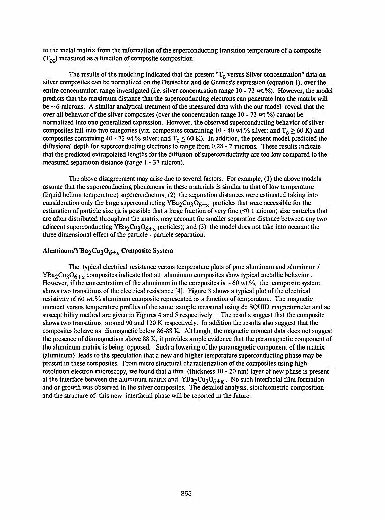
to the metal matrix from the informationof the superconductingtransitiontemperatureof a composite(Tcc) measuredas a function of composite composition.
The resultsof the modeling indicatedthatthe present "Tc versus Silver concentration"dataonsilver composites can be normalizedon the Dcutschcrand de Gennes'sexpression (equation 1),over theentireconcentrationrangeinvestigated (i.e. silver concentrationrange l0 - 72 wt.%). However,the modelpredictsthatthe maximum distancethat the superconductingelectrons can penetrate into the matrixwillbe - 6 microns. A similaranalyticaltreatmentof the measureddata with the ourmodel reveal that theoverall behaviorof the silver composites (overthe concentrationrange 10 - 72 wt.%) cannot benormalized into one generalizedexpression. However,the observedsuperconductingbehaviorof silvercomposites fall into two categories(viz. composites containing 10 - 40 wt.% silver; and Tc > 60 K) andcomposites containing 40 - 72 wt.%silver;and Tc _<60 K). In addition, the presentmodel predictedthediffusionaldepth for superconductingelectrons to range from0.28 - 2 microns. These results indicatethat the predicted extrapolated lengthsfor the diffusionof superconductivityaretoo low comparedto themeasuredseparationdistance(range 1 - 37 micron).
The abovedisagreementmay arise due to severalfactors. Forexample, (1) the above modelsassume that the superconductingphenomena in these materials is similar to that of low temperature(liquid helium temperature)superconductors;(2) the separationdistances were estimated taking intoconsiderationonly the large superconductingYBa2Cu306+x particles that were accessible for theestimationof particlesize (it is possible thata large fractionof veryfine (<0.1 micron)size particles thatareoften distributedthroughoutthe matrixmay accountforsmaller separationdistance between any twoadjacentsuperconductingYBa2Cu306+x particles); and (3) the model does nottake into accountthethree dimensional effect of the particle- particle separation.
Aluminum/YBa2Cu306+ x Composite System
The typicalelectricalresistanceversus temperatureplots of purealuminum and aluminum/YBa2Cu306+ x compositesindicatethatall aluminumcomposites show typical metallic behavior.However, if the concentration of the aluminum in the composites is _ 60 wt.%, the composite systemshows two transitions of the electrical resistance [4]. Figure 3 shows a typical plot of the electricalresistivity of 60 wt.% aluminum composite represented as a function of temperature. The magneticmoment versus temperature profiles of the same sample measured using dc SQUID magnetometer and acsusceptibility method are given in Figures 4 and 5 respectively. The results suggest that the compositeshows two transitions around 90 and 120 K respectively. In addition the results also suggest that thecomposites behave as diamagnetic below 86-88 K. Although, the magnetic moment data does not suggestthe presence of diamagnetism above 88 K, it provides ample evidence that the paramagnetic component ofthe aluminum matrix is being opposed. Such a lowering of the paramagnetic component of the matrix(aluminum) leads to the speculation that a new and higher temperature superconducting phase may bepresent in these composites. From micro structural characterization of the composites using highresolution electron microscopy, we found that a thin (thickness 10 - 20 nm) layer of new phase is presentat the interface between the aluminum matrix and YBa2Cu306+ x . No such interfacial film formationand or growth was observed in the silver composites. The detailed analysis, stoichiometric compositionand the structure of this new interfacial phase will be reported in the future.
265
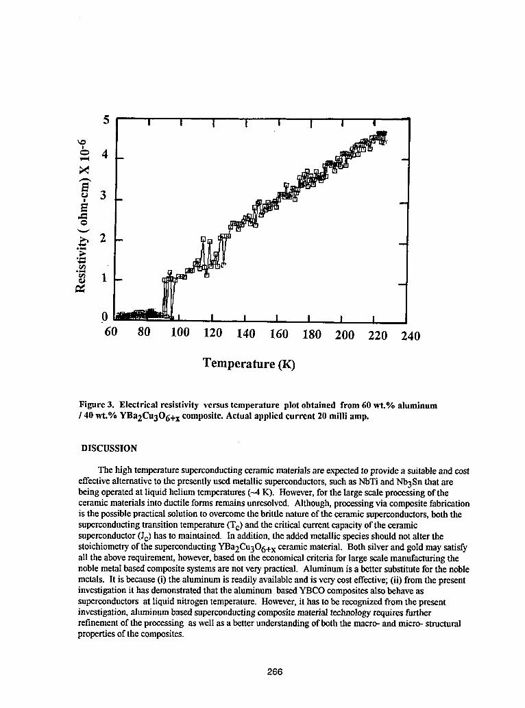
0
60 80 100 120 140 160 180 200 220 240
Temperature (K)
Figure 3. Electrical resistivity versustemperature plotobtained from 60wt.% aluminum/ 40wt.% YBa2Cu306+x composite.Actualappliedcurrent20 milli amp.
DISCUSSION
The high temperaturesuperconductingceramicmaterials are ex_,cted to providea suitableandcosteffective alternativeto the presentlyused metallicsuperconductors,such as NbTi andNb3Sn that arebeing operatedat liquidhelium temperatures(--4 K). However,for the large scale processingof theceramic materials into ductile formsremainsunresolved. Although, processingvia composite fabricationis the possible practicalsolution to overcomethe brittlenatureof the ceramicsuperconductors,both thesuperconductingtransitiontemperature (Tc)and the critical currentcapacityof the ceramicsuperconductor(Jc) has to maintained. In addition, the addedmetallic species should notalter thestoichiometryof the superconductingYBa2Cu306+x ceramicmaterial. Both silver and gold maysatisfyall the above requirement,however,basedon the economical criteria for large scale manufacturingthenoble metalbased composite systemsarenotverypractical. Aluminumis a bettersubstitutefor the noblemetals. It is because (i) the aluminumis readilyavailableand is very cost effective; (ii) from the presentinvestigation it has demonstratedthat the aluminum basedYBCO compositesalso behave assuperconductors at liquid nitrogen temperature. However,it has to be recognizedfrom the presentinvestigation,aluminum based superconductingcompositematerialtechnology requiresfurtherrefinementof the processing as well as a betterunderstandingof both the macro- and micro- structuralpropertiesof the composites.
266
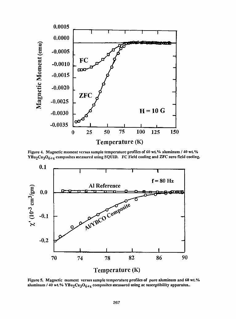
0.0005I ; t I
0.0000
-0.0005
"_ -0.0010 FC
N -o.ools.mut -0.0020
o 2Y-0.0025-0.0030 - H = 10 G i
-0.0035 I I I I I0 25 50 75 100 125 150
Temperature (K)Figure 4. Magnetic moment versus sample temperature profiles of 60 wt.% aluminum / 40 wt.%YBa2Cu306+ x composites measured using SQUID. FC Field cooling and ZFC zero field cooling.
0.1I I i t
f=80 Hz
_- A! Reference
.o.,_
-0.2
I I I !70 74 78 82 86 90
Temperature (K)Figure 5. Magnetic moment versus sample temperature profiles of pure aluminum and 60 wt.%aluminum / 40 wt.% YBa2Cu306+ x composites measured using ac susceptibility apparatus..
267
CONCLUSION
From the present investigation the following conclusions can be derived :
1. The addition of silver to the YBa2Cu306+x does not affect the superconducting behavior ofYBa2Cu306+ x over the entire concentration range of I0 - 72 wt.% silver. However the Tc decreases fromTc 77 K to 60 K with an increase in the concentration of silver above 40 wt.% to 72 wt.%.
2. Although, the theoretical models based on classical proximity theory of low temperaturesuperconductors can predict the lowering of Tc with the increase in the concentration of silverin thecomposites, the extrapolated length for the diffusion of superconductivityfrom YBa2Cu306+ x into silvermatrixpredicted from the theoryare not agreeable with the experimentally determined superconductingYBa2Cu306+ x particle - particle separation distance.
3. 60 wt.% Aluminum/YBa2Cu306+x compositesbehaveas superconductorsand these compositesshowtwo transitionsaround90 and 120K respectively.
ACKNOWLEDGMENT : The author would like to thank Drs. O. P. Arora, L. F. Aprigliano, A.Purohit (ANL) and C. S. Pande (NRL) for their valuable suggestions and useful discussions, and Dr. B.Douglas, Director of Research, CDNSWC for funding this project under ONR sponsored ILIR Program.
REFERENCES
1. Hepp, A. F., Gaier, J. R., Hambourger,P. D. and Pouch, J. J., "Interactionof Au,
Ag, and Bi Ions with YBa2Cu307.y : Implications forSuperconductorApplications," Processing and Applications of High Tc Superconductors,edt. W.E. Mayo, Pub. The Metallurgical Society, 213 (1988).
2. Sen, S., In-Gann Chen, Chen, C. H. and Stefanescu, D. M., "Fabricationof StableSuperconductiveWires with YBa2Cu306+ x/Ag20 Composite Core," Appl. Phys. Letts., 54(8),766 (1989).
3. Rao, A. S., Aprigliano, L. F. and Arora, O. P., "Effect of the Additives on Morphology andSuperconductivity ofYBa2Cu306+ x Ceramic materials," Bull. Mater. Sci., 14(2), 269 (1991)
4. Rao, A. S. "Processing and Property Evaluation of YBa2Cu306+ x / Aluminum Composites,"Applied Superconductivity, 113-61,725 (1993).
5. Rao, A. S. "Properties of Superconducting YBa2Cu306+ x Ceramic Materials : Effect ofProcessing Parameters," Applied Superconductivity, 113-61,607(1993).
6. Rao, A. S., Arora, O. P. and Pande, C. S., " Superconductivity in YBCO / Al Composite System,"Physica C, 224, 221 (1994).
7. Deutscher, G., and de Gennes, P. G.., "Proximity Effects," in Superconductivity, edt. Parks, R.D.,Pub. Macel Dekker, Inc., New York, NY, 2, 1005 (1969).
268

THIS PAGE INTENTIONALLY LEFT BLANK


Physical Properties
Session PP-1 Chair: Prof. Valeri OzhoginCo-Chair. Prof Evgenii Z. Meilikhov

ELECTRONIC PROPERTIES OF Y-Ba-Cu-O SUPERCONDUCTORSAS SEEN BY Cu and O NMR/NQR
D. Brinkmann
Physik-Institut, University of ZfirichWinterthurerstrasse 190, 8057 Zfirich, Switzerland
Abstract Nuclear Magnetic Resonance (NMR) and Nuclear Quadrupole Res-onance (NQR) allow the investigation of electronic properties at the atomic level.We will report on such studies of typical members of the the Y-Ba-Cu-O familysuch as YBa2Cu306+, (1-2-3-(6+x)), YBa2Cu4Os (1-2-4) and Y2Ba4CuTO15(2-4-7) with many examples of recent work performed in our laboratory. In particular,we will deal with Knight shift and relaxation studies of copper and oxygen. Wewill discuss importa:nt issues of current studies such as: (1) Existence of a com-mon electronic spin-susceptibility in the planes (and perhaps in the chains) of1-2-4. (2) Strong evidence for the existence of a pseudo spin-gap of the anti-ferromagnetic fluctuations in 1-2-4 and 2-4-7. (3) Evidence for d-wave pairingin 1-2-4. (4) Strong coupling of inequivalent Cu-O planes in 2-4-7 and possibleorigin for the high Tc value of this compound. (5) The possibility to describeNMR data in the framework of a charge-excitation picture.
1. Introduction
While there is not yet a generally accepted theory of the mechanism of high-temperature superconductivity (HTSC) experiments have provided a wealth ofsound data and relevant information which wait for proper and adequate inter-pretation. Among the techniques which probe properties on the atomic scale,are Nuclear Magnetic Resonance (NMR) and Nuclear Quadrupole Resonance(NQR). How these disciplines obtain their informations and what the results andissues are, at least for the Y-Ba:Cu-O and the La-Sr-Cu-O families of HTSC, hasbeen reviewed recently [1]. A collection of articles on NMR/NQR applications inHTSC from many leading groups in the field may be found in a special issue ofApplied Magnetic Resonance [2]. Recent short reviews of our work emphasizingY-Ba-Cu-O compounds deal with either crystallographic and materials scienceaspects [3]or relaxation [4].
In this paper we review some of the results gathered in our laboratory. Theyare concerned with several issues presently under debate in the HTSC commu-nity: (i) the existence of a single-spin fluid in the Cu-O planes and chains; (ii) thespin-gap effect; (iii) the orbital symmetry of the pair-wave function; (iv) the cou-pling between CuO2 planes; (v) the possibility to describe NMR data within theframework of a charge-excitation picture. Our answers are based on new Knightshift and NMR/NQR spin-lattice and spin-spin relaxation data for YBa2Cu4Osand Y2Ba4CuTO15.
273
2. The single-spin fluid model
Many properties of the cuprates are intimately connected with the fact that
the parent structure of these compounds is an anti-ferromagnet, namelyYBa2Cu306+_ which has a Ndel temperature of TN = 415 K for x = 0. Introduc-
ing oxygen destroys the long-range anti-ferromagnetic (AF) order. However, the
Cu electron spins still exhibit short-range AF spin fluctuations which give rise to
a frequency (w) and wave-vector (_ dependent dynamic electronic susceptibility
The question arises whether the susceptibilities associated with the Cu spinand the oxygen hole are independent of each other or not. This can be answered
by Knight shift measurements. The NMR line shift due to magnetic interactions
is expressed by the magnetic shift tensor K, whose components (in a reference
frame a = x, y, z), can be decomposed into a spin, an orbital and a diamagneticpart:
K_(T) = h'svintT_ + h"°rb + h"di_- - _ CX \--1 - - CXCX - - or _ "
In HTSC compounds, [,[orb is predominantly temperature independent, whereas
the temperature dependent K spin is expected to vanish in the superconductingstate due to singlet spin pairing. K dia is small and can be neglected quite often.
Each tensor can be expressed by the respective hyperfine interaction tensorand the static electronic susceptibility (i.e. at zero wave vector and zero fre-quency) as:
gl_B j
For the analysis of the data, we introduce the following notations. Kcc denotes
the tensor component perpendicular to the CuO2 planes (B0 [[ c), while the in-
plane components of the shift are given by KII and K., where B0 is parallel andperpendicular to the CuO-bond axis, respectively. We define the axial spin part
of h" as K_ i_ = (1/3!(KI_Pi _ - g_pi_). The equivalent definition for the isotropic
spin part of K is K,-'_o''_ = (1/3)(KI_Pi'_ + K__pi'_+K_pi").The new measurements of the planar Cu and 0 Knight shifts [5] enlarge and
improve our previous data [6,1]. Various Cu and O shift components can be
calculated from the data, the result is shown in Fig. 1. While in a "classical"superconductor like aluminum the Knight shift stays constant in the normal state
and starts to decline at T_, the Knight shift components of YBa2Cu40s begin todecrease already well above To. This behavior is typical for under-doped HTSC
[1], i.e. for compounds whose doping level is below the value that corresponds
to a maximum T_. In addition, all components exhibit the same temperaturedependence. These facts support the "single-spin fluid" model which states that
the Cu-d holes and the doped holes (which mainly go into O-2p states) have onespin degree of freedom.
Our YBa2Cu40s shift data resemble very much those for YBa2Cu306.s3 [7]thus demonstrating again that both compounds are under-doped. Similar *tO
274
shift data for YBa2Cu40s were reported by Machi et al. [8] and similar CuKnight shift data were obtained in Bi2Sr2CaCu20s [9]. The existence of a planarsingle-spin fluid had also been deduced from Y and T1 NMR [1]. The concept isnow well established.
A single-spin fluid seems to exist also in the chains of YBa2Cu40s [5]. Thecomponents of both the Cul and O1 Knight shift decrease below Tc although thisis less pronounced for the K_ component. All K components of Cul are propor-tional to the respective component of O1, which again points to the existence ofa single-spin fluid. However, the susceptibilities of planes and chains are different.
3. The spin-gap effect
The study of spin-lattice (and spin-spin) relaxation in HTSC is intimatelyconnected with the question about the origin of superconductivity in these ma-terials, although not in a simple straightforward manner. For instance, somegroups have proposed that superconductivity is induced by electron spin fluctu-ations [10]. The relevance of these fluctuations in neutron scattering and NMRrelaxation experiments is well established [1]. Nearly all mechanisms which areresponsible for spin-lattice relaxation in HTSC are based on electron-nuclear in-teractions. The only exception seems to be the Ba relaxation in YBa2Cu40s[1,11] which is due to the two-phonon Raman process, i.e. a coupling betweenphonons and the Ba quadrupole moment.
Thus, for Cu, 0 and Y the relaxation is described by the Moriya formulawhich relates the relaxation rate to the hyperfine fields and the dynamical electronsusceptibility:
1( )0- 2t_'---_B_ [iA _,(q-) (1)O',a#a' COl
Here, i denotes the nuclear species and coi is its NMR frequency. The magneticfield B0 is oriented along the a direction which coincides with one of the crystallo-graphic axes (a,b,c). X_,_,(q-',wi)is the imaginary (dissipative) part of X. A_,(q-)are formfactors related to the hyperfine fields. Eq.(1) demonstrates that thespin-lattice relaxation provides a tool to probe the average over the q-dependentelectron susceptibility.
As an example, Fig. 2 shows the temperature dependence of the relaxationrate per Kelvin for the planar Cu and 0 nuclei in YBa2Cu40s [5]. 6a(T1T)-Ireaches a maximum around 130 K and rapidly decreases towards lower tempera-tures. On the other side, 17(T1T)-I displays a monotonous decrease with loweringtemperature. These are typical behaviors found in oxygen-deficient YBa2Cu306+_and, thus, may be taken as signature of under-doped material.
A good starting point for explaining these data is the the phenomenologicalMillis-Monien-Pines model [12,1]. It is assumed that there is a direct hyperfineinteraction between the Cu2 nuclei and an electron of the on-site 3d_2_y2orbital
275
and a transferred interaction with electrons of the 3d=2_u2 orbitals of the fourneighboring copper ions. For the planar oxygen nuclei, there exists a transferred
hyperfine coupling. The electron spins themselves interact anti-ferromagnetically.The electronic spin fluctuations peak near Q = (_r/a, 7r/a) which is the AF order-
ing point in _'-space. Since the 0 and Y formfactors entering into Eq.(1) vanish at
q = Q, the different behavior of Cu, O and Y relaxation rates can be explained.
Further progress in understanding the Cu relaxation behavior was triggeredin two ways. First, Millis and Monien [13] suggested that the spectral weight
in the spin fluctuations decreases as the temperature is lowered. This missingspectral weight must reappear at a higher energy in the form of a transition
over a "spin pseudo-gap", A. While the AF fluctuations increase with fallingtemperature and hence increase 1/T1T, there will be a temperature where the
spin gap effect wins and 1/T1T will decrease; this explains the maximum of
1/T1T for Cu. Secondly, Rossat-Mignod et al. [14] were the first to discover
the spin-gap effect in YBa_Cu306+= by neutron scattering where the results forx"(Q,w) resemble very much the 1/TIT data.
When describing the spin-lattice relaxation rate in terms of the spin-gap effectit became customary [1,15,16] to use the following ad hoc formula:
1 o[:_ (A.F11T,T- (_) tanh2 \-2-T---], (2)
Here, A0 is a constant. AAF denotes the spin-gap energy at Q. The factor T -_ isintroduced to assure a reasonable description of the high-temperature behavior.
We have fitted Eq.(2) to the planar Cu relaxation data of both the YBa2Cu4Os
[5] and the Y2Ba4CurO15 [1,16] structure, the latter case is shown in Fig. 3. Thefit parameters for both Cu sites, Cu2 and Cu3, are A = 240 + 20 K and a =1.25 and thus agree within the error limits with A = 260 =i=10 K and a = 1.25
we obtained for the fit to the Cu2 data in YBa2Cu4Os. We will return to thispoint later.
The Knight shift data have also been fitted by a spin-gap formula, similar toEq.(2), namely by
K = Ko [i- tanh'(2_) ] (3)
where Ao referstothe gap atzerowave vector.Our fitto theYBa2Cu4Os data
yields A0= 180 K which is in good agreement with the neutron scattering result.
If the temperature variation of the Knight shift is really due to the opening of aspin-gap and Eq.(3) is appropriate for analyzing the data, the result implies thata spin-gap opens also at q = 0 and that this values is different from the AAF value.
4. The symmetry of the pair-wave function
Whether thespatial symmetry of the pairing state is a s-wave or d-wave isa controversial topic. This is not the place to deal with all the aspects of this
276
problem, we just focus on various possibilities NMR/NQR offer to check thissymmetry, in particular in YBa2Cu3OT and YBa2Cu4Os .
One way is to study the anisotropy of the relaxation rate, that is the ratior = 6aT_/63T_b of the Cu relaxation rate in the superconducting state wherec and ab specify the orientation of the applied magnetic field, /30. Detailedtheoretical analyses of the relaxation data for YBa2Cu307 [17,18] revealed thatthe temperature variation of r is not compatible with s-wave pairing and favorsd-wave symmetry. Our YBa2Cu4Os data [19] are in qualitative agreement withthe YBa2Cu3OT data and thus also favor d-wave symmetry.
A very promising check of the pairing state symmetry is the measurementof the copper and oxygen relaxation rates at very low temperatures. Both ratesdisplay a power-law behavior, i.e. 1/7'1 cxT n with n between 2.5 and 3 as recentlyobserved for YBa2Cu307 [20] and YBa2Cu4Os [5]. This points to the existence ofnodes in the superconducting gap as one expects, for instance, for d-wave pairingsuperconductivity [21].
Last but not least, the Knight shift may reveal the pairing state symmetryprovided the data are accurate enough. For instance, the chain Cul Knight shiftdata in YBa2Cu307 [22] and YBa2Cu408 [5] can not satisfactorily be fitted byan s-wave expression while an d-wave fit is perfect for the YBa2CuaOr data. Al-though the theoretical expression for YBa2Cu4Os has not yet been calculated thesimilarity between data of both structures suggests that in both cases the d-waveexpression provides the better fit. Thus, one may conclude that NMR/NQR datafavor d-wave symmetry at least in the YBa2Cu3Oz and YBa2Cu4Os structures ofthe Y-Ba-Cu-O family.
5. Inter-plane coupling
One of the key issues in understanding HTSC is the question whether a cou-pling between CuO2 planes favors or impedes superconductivity. Before specu-lating in one or the other direction, it is necessary to prove that an inter-planecoupling exists. As far as NMR/NQR is concerned, the multi-layer structureY2Ba4CurOxs with its alternating 1-2-3 and 1-2-4 blocks offers the unique possi-bility to study the coupling between inequivalent CuO2 planes.
We have studied the relaxation rates and the Knight shifts of the Cu2 andCu3 sites in the 1-2-3 and 1-2-4 block, respectively, of the Y2Ba4CurOxs com-pound [1,16]. It turned out that the ratios of these quantities are constant aboveTo. Thus, both the static and the dynamic electron spin susceptibilities of theindividual planes of a double-plane are governed by the same temperature de-pendence. This implies the existence of common spin dynamics in both planes,and hence these planes must be strongly coupled. Despite their coupling, theirspin susceptibilities retain a distinct q dependence. The presence of the couplinghas also been demonstrated by performing SEDOR (spin-echo double resonance)experiments on the Cu2 and Cu3 nuclei [23].
277
Below To, the common temperature dependence is lost, which could arisefrom the opening of two superconducting energy gaps that differ in the individualplanes, thus revealing the different plane charge carrier densities of the 1-2-3 and1-2-4 block. This difference in doping levels had also been inferred from thetemperature dependence of the Cu2 and Cu3 NQR frequencies. We found thatthe 1-2-3 block is less doped than the pure YBa2CuaOr compound, hence thedoping level of the 1-2-3 block is closer to optimal doping. If one simply assumesthat the block with the highest Tc "wins", then this would explain the high To,namely 93 K, of the Y2Ba4CurO15 compound.
As mentioned above and shown in Fig. 3, the Cu2 and Cu3 relaxation ratesin Y2Ba4Cu7015 could be fitted by the spin-gap formula Eq.(2) with the sameparameters for both data sets. The fact that these values are the same as thoseused for the fit of the YBa2Cu4Os relaxation data, demonstrates the very similarspin dynamics in YBa_Cu4Os and Y2Ba4CuTO15and that the doping level of theblocks in Y2Ba4CuTOls are close to optimal doping.
6. Hubbard model with magnetic exchange
The excellent fit of the spin-gap expression to the planar Cu relaxation datain YBa2Cu40s and Y2Ba4Cu7Ols certainly cannot "prove" that the relaxation
arises from the spin-gap effect. Other physical phenomena in HTSC need to be
explained by this effect. As an alternative to explain Knight shift and relaxationdata we conclude our survey by drawing the attention to an approach which is
a variant of the Hubbard model comprising magnetic exchange in second order
between copper and oxygen holes [24]. The exchange gives rise to a new singletcorrelated band separated from the oxygen band. The energy spectrum has been
calculated. The low energy physics is determined by a high density of chargeexcitations in the singlet impurity band together with spin excitations in the
lower Hubbard band. Taking an idealized density of states, an analytical form isobtained for the temperature dependent susceptibility:
X" 1 [1 - tanh 2 (po -aT'_]cx _ \ ksT /J
where the factor a = 0.4 x 10⁻⁴ eV/K of the chemical potential is not a fit param-eter. This expression perfectly describes the Cu2 relaxation rate in YBa2Cu40sfrom Tc up to 600 K.
These examples clearly show that the debate about the proper description ofspin-lattice relaxation in HTSC, at least of the Y-Ba-Cu-O type, is not yet closed.
References
278
[1] Brinkmann D., Mali M.: NMR Basic Principles and Progress 31,171 (1994)[2] appl. Magn.Reson.a, as3- 75o(1992)[3] Brinkmann D: in: Proc. of the 20th Intern. School of Crystallography (KaldisE., ed.), Kluwer academic Publ., 225 (1994)[4] Brinkmann D. in: Proc. of 2nd Internat. Discussion Meeting on Relaxationin Complex Systems (Ngai K., ed.), Alicante (Spain), 1993, J. Non-CrystallineSolids, in press[5] Bankay M., Mall M., Roos J., Brinkmann D.: Phys. Rev. B, in press[6] Mangelschots I., Mali M., Roos J., Brinkmann D., Rusiecki S., Karpinski J.,Kaldis E.: Physica C 194, 277 (1992)[7] Takigawa M., Reyes A.P.,' Hammel P.C., Thompson J.D., Heffner R.H., FiskZ., Ott K.C.: Phys. Rev. B 43, 247 (1991)[8]Machi T., Tomeno I., Miyatake T., Koshizuka N., Tanaka S., Imai T., YasuokaH.: Physiea C 173, 32 (1990)[9] Walstedt R.E., Bell R.F., Mitzi D.B.: Phys. Rev. B 44, 7760 (1991)[10] Monthoux P., Pines D.: Phys. Rev. Lett. 69, 961 (1992)[11] Lombardi A., Mali M., Roos J., Brinkmann D., Yakubovskii A.: Submittedto 4th Intern. Conference on Materials and Mechanisms of SuperconductivityHigh-Temperature Superconductors (M2S-HTSC-IV), Grenoble (July 1994)[12] Millis A.J., Monien H., Pines D.: Phys. Rev. B 42, 167 (1990)[13] Millis A.J., Monien H.: Phys. Rev. B 45, 3059 (1992)[14] Rossat-Mignod J., Regnault L.P., Vettier C., Burlet P., Henry J.Y., LapertodG.:, Physica B 169, 58 (1991)[151Mehring M.: Appl. Magn. Reson. 3, 383 (1992)[16] Stern R., Mall M., Mangelschots I., Roos J., Brinkmann D., Genoud J.-Y.,Graf T., Muller J.: Phys. Rev. B (1 July 1994)[17]Martindale J.A., Barrett S.E., Klug C.A., O'Hara K.E., DeSoto S.M., SlichterC.P., Friedmann T.A., Ginsberg D.M.: Phys. Rev. Left. 68, 702 (1992)[18] Takigawa M., Smith J.L., Hulst W.L.: Phys. Rev. B 44, 7764 (1991)[19] Bankay M., Mall M., Roos J., MangelschotS I., Brinkmann D.: Phys. Rev.B 46, 11228 (1992)[20] Martindale J.A., Barrett S.E., O'Hara K.E., Slichter C.P., Lee W.C., Gins-berg D.M.: Phys. Rev. B 47, 9155 (1993)[21] Bulut N., Scalapino D.J.: Phys. Rev. Lett. 68, 706 (1992)[22] Slichter C.P., Barrett S.E., Martindale J.A., Durand D.J., Pennington C.H.,Klug C.A., O'Hara K.E., DeSoto S.M., Imai T., Rice J.P., Friedmann T.A.,Ginsberg D.M.: Appl. Magn. Reson. 3, 423 (1992)[23] Mall M., Roos J., Stern R., Brinkmann D., to be submitted to Phys. Rev.Lett.
[24] Eremin M.V., Varlamov S.V., Solovjanov S.G., Brinkmann D., Mali M.,Markendorf R., Roos J.: Submitted to 4th Intern. Conference on Materialsand Mechanisms of Superconductivity High-Temperature Superconductors (M2S-HTSC-IV), Grenoble (July 1994)
279
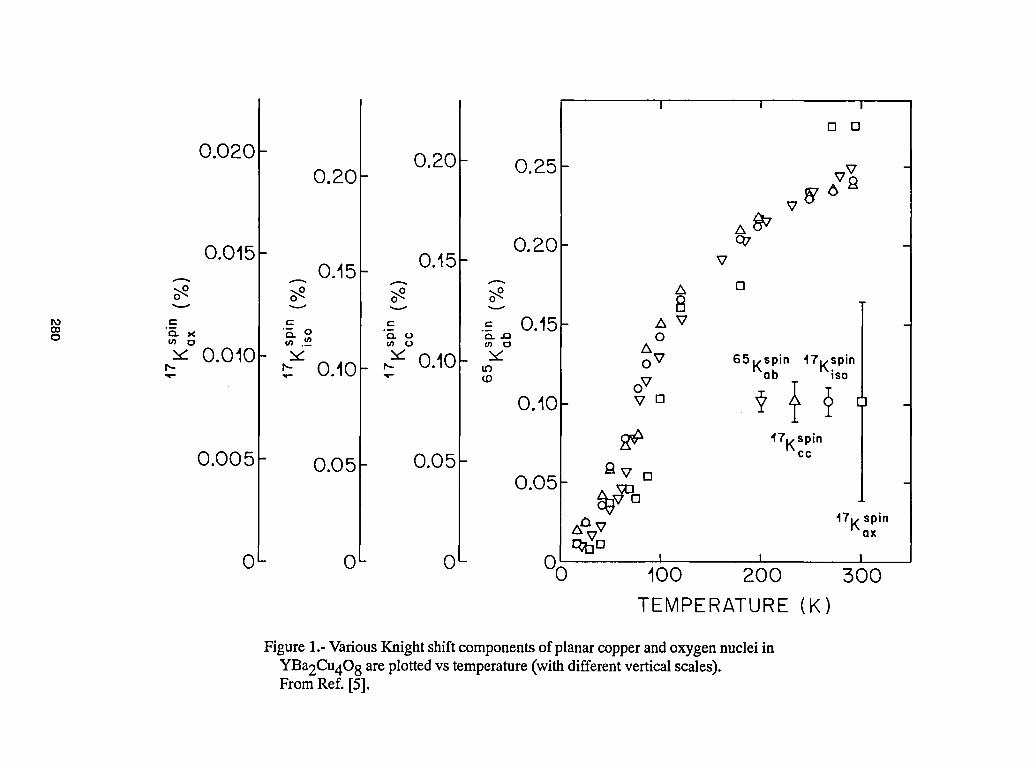
TEMPERATURE ( K )
Figure 1.- Various Knight shift components of planar copper and oxygen nuclei in YBa2Cu4O8 are plotted vs temperature (with different vertical scales). From Ref. [5] .
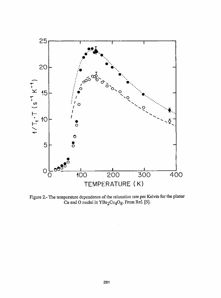
_,J I I I
°° • 0Oooo
20- .-. -:O ..
: _o(_.. "-.• ..
"-" - 00 0",, O,.I - l 0", ""
: 0 O\ ".."" 15- .o o .. _
: / \"0 O....I _ ".°
:1 0 _, ...or)I _0 "'. i
F- I " "'-..
"_10- I "_.,.I- • ""_@ --.
o
5- •0 -
_oeeO0 n n ,'100 200 :.500 400
TEMPERATURE (K)
Figure 2.- The temperature dependenceof the relaxationrate per Kelvinfor the planarCu and O nuclei in YBa2Cu408. From Ref. [5].
281
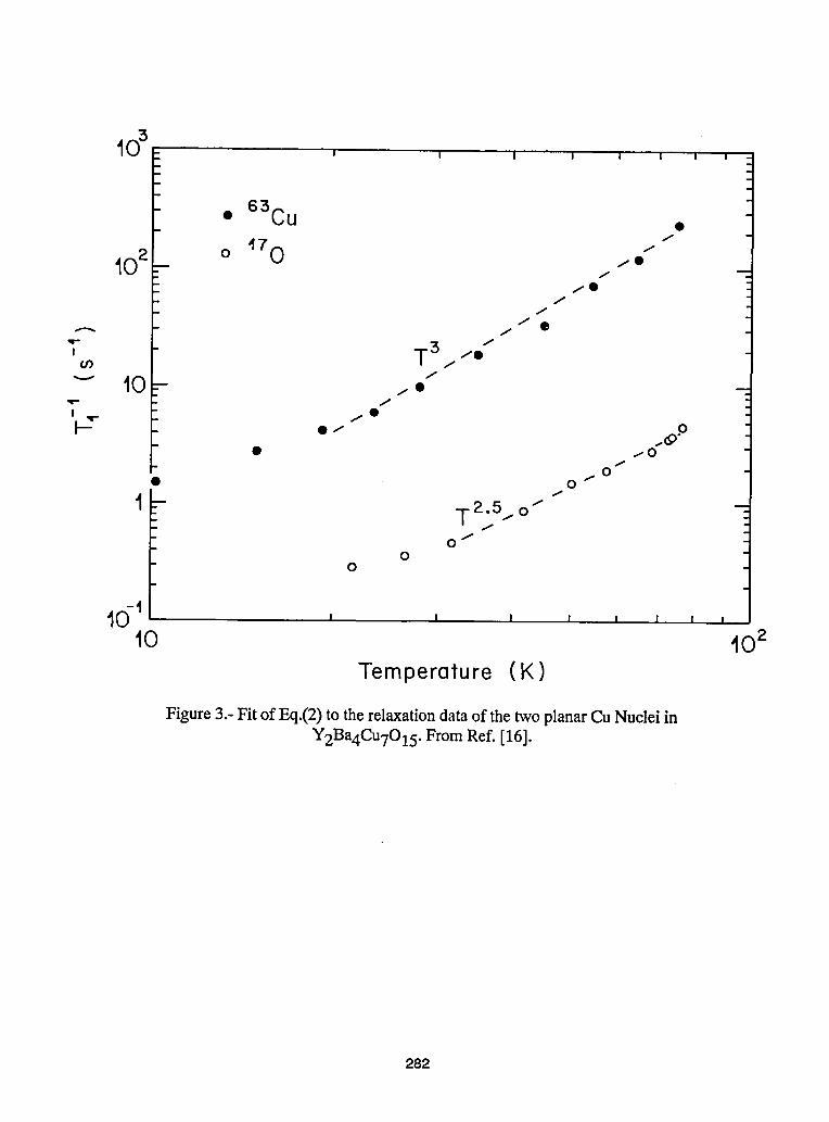
0 _ - I I I I I l I I -
• 63Cu •/
10a_ o 470 _o_0
f
o
-- T3 -"
10 - ..o _
• /0
0• 0 _
1 - T2.51 o_ -o
oo
10 -t I I I I I I I I
10 102Temperature (K)
Figure 3.- Fit of Eq.(2) to the relaxation data of the two planar Cu Nuclei inY2Ba4Cu7015. From Ref. [16].
282
Quaternary Borocarbides - New Class of Intermetallic Superconductors
R. Nagarajan I , L.C. Gupta 1, S.K. Dhar1, Chandan Mazumdar 2, Zakir Hossain 1,C. Godart 3, C. Levy-Clement 4, B.D. Padalia 2 and R. Vijayaraghavan 1
1Tara Institute of Fundanlental Research, Bombay - 400 005, India.2Department of Physics, Indian Institute of Technology, Bombay 400 076, India.
3UPR-209, C.N.R.S., Meuaon Cedex, 92195, France.4Laboratoire Physique Solides, C.N.R.S., Meudon Cedex, 92195 France.
Abstract
Our recent discoveryof superconductivity(SC) in the four-elementmultiphaseY-Ni-B-C system at
an elevated temperature (Tc-12K) has opened up great possibilities of identifying new superconductingmaterials and generating new physics. SuperconductivitywithTc (> 20 K) higher than that known so far inbulk intermetallics has been observed in multiphase Y-Pd-B-C and Th-Pd-B-C systems and a family of
single phase materials RENi2B2C (RE= Y, rare earth) havebeen found. Our investigations show YNi2B2Cto be a strongcoupling hard type-IISC. Hc2(T) exhibitsanunconventionaltemperaturedependence. Specificheat and magnetization studies revealcoexistence of SC and magnetismin RNi2B2C (R = Ho, Er, Tm) withmagneticorderingtemperatures(Tc-8 K, 10.5K, 11K andTm-5 K, -7 K, -4 K respectively)that areremarka-bly higherthan those in known magnetic superconductors. I.t-SRstudies suggest the possibility of Ni atomscarryinga moment inTmNi2B2C. Resistivityresultssuggestsa doublere-entrant transition (SC-normal-SC)in HoNi2B2C. RENi2B2C (RE = Ce, Nd, Gd) do not showSC down to 4.2K. The Nd- and Gd- compoundsorder magneticallyat -4.5 K and -19.5 K, respectively.Two SC transitions are observed in Y-Pd-B-C (Tc-22 K, -10 K) and in Th-Pd-B-C(Tc -20 K, -14 K) systems,whichindicatethat there are atleast two struc-lures which support SC in theseborocarbides.In our multiphaseThNi2B2C we observe SC at -6 K. No SCwas seen in multiphase UNi2B2C, UPd2B2C, UOs2Ge2C and UPd5B3C0.35 down to 4.2K. Tc inYNi2B2C is depressed by substitutions(Gd,Th and U at Y- sites and Fe, Co at Ni-sites).
1. Introduction.
Our recent discovery of superconductivity in Y-Ni-B-C [1-4], with T e -12 K to 15 K, which isrelatively high superconducting critical temperature for intermetallics, has triggered an intense activity in theareas of superconductivity and magnetism. This discovery came about as a result of our on going investiga-tions in Ni-based systems [5, 6]. An extension of Y-Ni-B-C system - going froma 3d- to 4d- element- led to theobservation of record Tc (-23K [7], 22K [8]) in multiphase Y-Pd-B-C system. It may not be out of place toremark that a similar situation occurreddufing the initial phase of the discove_ryof high-T c superconductivi-ty. Super'conductivity was observed in_amultip.hase material La-Ba-Cu-O with a relatively low T c (-30K) [9]and later, superconductivity was reported in a multiphase material Y-Ba-Cu-O with a much higher Tc(-93 K) [10].
We have been investigating Ni-based intermetallics for more than a decade in search of new valencefluctuation (VF) systems, besides our being interested in their magnetic and transport properties. We suc-ceeded in identifying a number of new Ni-based VF systems such as EuNi2P 2 [11], EuNiSi 2 [12],
Eu2Ni3Si 5 [13], Ce2Ni3Si 5 [14]. Discovery of the above Eu-based VF compounds is particularly significant,as not many stoichiometric Eu-compounds exhibiting VF are known even today. After the discovery of high-
Tc superconductors, Ni-based materials acquired additional significance. All high-T c oxide superconductors,except Bal.xKxBiO 3 [15], contain C'uas an essential component. As is well known, Ni-based oxides such asNiO and La2NiO 4 are Mott-Hubbard insulators (just as CuO and La2CuO 4 are), and attempts to induce SOin the nickel oxides failed. Moreover, partial Ni-substitution in cuprate superconductors suppressed T c. Thus,nickel did not seem to favour superconductivily in oxides. On the other hand, in most Ni-based intermetal-
283
lics,Ni-momentis quenchedand,therefore,theyarepotentialcandidatesforsuperconductivity.
Ni-containingborideseriesRNi4B(R=rareearth)wastakenupby us forinvestigation,as manyternaryrareearth-transitionmetalborideswere knowntosupportSC. Someof themareevenmagneticsuperconductors,exhibitingcoexistenceofSC andmagnetism.RNi4Bseriesturnedouttobe remarkableasweobservedvariousphenomenain thesameseries,viz.,VFin CeNi4B116],anomalouslyhighferromagnet-icorderingtemperature(=39K)in SmNi4B[5,6, 17] ascomparedto thatofGdNi4B(=36K)[5,6, 17]andweaksignalsof superconductivityin oursamplesofYNi4B[1].Ourfurtherworkshowedthat superconduc-tivityin YNi4Boriginateddueto thepresenceof carbonwhichstabilizesa SCphase in the material.Wepresentbelowfurtherdetailsof ourdiscoveryof superconductivityin Y-Ni-B-Csystemand someof ourrecentresultsontheborocarbidesuperconductors.
2.Discoveryof Superconductivityin Y-Ni-B-CSystem.
YNi4BcrystallizesinthehexagonalCeCo4Btypestructure(spacegroupP6/mmm)[18]andis alsoreportedto havea superstructure(a'= 3a0;c =Co)in itslattice[19].WesynthesizedYNi4Bbystandardarcmeltingtechnique.Powderx-raydiffraction(XRD)patternof thematerialconfirmedthe formationof thematerialin singlephasebelongingtotheabovementionedstructure.The latticeconstantsobtainedfromRietveldanalysis,includingasuperstructure,ofourXRDpatternyieldedlatticeparametersas:a = 14.96(5)c= 6.95(2)._ [1],whichagreewellwiththe publishedvalues[19].
MagneticsusceptibilityofoursampleofYNi4B,measuredasa functionoftemperaturein a fieldof4000G,showeda sharpdropnear12K [1,6] (Fig.1).Thisdropis notthatof atypicalantiferromagnetbe-cause,thedropis rathersharpandsusceptibilityincreasesonfurthercoolingofthesample.Resistivityof oursampleasa functionof temperature(Fig.1)alsoshowsasharpdrop(butdoesnotgotozero)around12K,thesame temperaturewherethe dropin susceptibilityis seen [1].Thetwo observationstogetherindicatedthepossibilityofoccurrenceofsuperconductivityin thissample.MVsHmeasurementsclearlyshoweddiamag-netismat low field,confirmingoccurrenceof superconductivity.Reproducibilityof dropin resistivitywasconfirmedbystudyingmanyindependentbatches(foroneofthem,thestartingmaterialswereobtainedfroma differentsource)of YNi4B[1].
M Vs.T measurements(Fig.3) at 65Gon asinglepieceof YNi4BC0.2 showedshieldingandtheMeissnerfractionstobe4%and1%respectively.PowderedmaterialalsoshoweddiamagneticresponseandMeissnereffect.Annealingof thesample,thoughdecreasedtheshieldingfraction,improvedMeissnerfrac-tionandTc (-15 K)(Fig.2).AstheSC fractionwassmall,thesamplewasexaminedforimpurityphasesbyenergydispersiveanalysisof x-rays(EDAX)andelectronmicroprobeanalysis.Thesamplewasessentiallyhomogeneousexceptforsomesmallinclusionswhichappearedto be Y203 andYNi5 (bothare non super-conducting).Nobinaryorternaryalloysof Y,Ni,B areknowntobesuperconductingwith sucha high Tc.Thus,observationof superconductivityat 12Kwasa newandsurprisingresult.
Lowvolumefractionof superconductivityimpliedthatthe entiresamplewas not superconductinganditwasnecessarytounderstandtheoriginof observedsuperconductivity.Weconsideredthepossibilityofcrystallographicsuperstructure[1]being responsibleforthisbehaviour.However,we alsoconsideredthepossibilityof theoriginof SC beingdueto a minorityphasestabilizedby thepresenceof a fourthelement.Carbonwasconsideredtobeonepossiblefourthelementwhichgotintroducedin thesystemunintentionally.In orderto checkthis,0.2atomfractionof carbonwasdeliberatelyaddedtoYNi4B,remeltedandthemateri-alwasstudied.Onadditionofcarbon,resistancedroppedtozeroaround12K(Fig.3)andthesuperconduct-ingshieldingfractiondramaticallyenhancedto nearly80%of perfectSC [4].Theseresultswereconfirmedon manyindependentlypreparedbatches.It becameclearthatcarbonplaysthecrucialrolein theobservedsuperconductivity.Presenceof carbonintroducesstructuralchangesas well;XRDpatternof YNi4BC0.2indicatedthatsuperstructureof YNi4Bgets suppressedascarbonisintroducedinthematerial[4].ThuS,onecouldarguethatcarbondoesnotplayanychemicalrole,itbringsin structuralchangesthatin turnarere-sponsiblefortheobservedsuperconductivity.TheobservedSCbeingdueto possibleformationof Y2C3,whichis a knownsuperconductor[20],wasruledouton thebasisof EDAXanalysisof thematerialandonotherconsiderations[4].
284
Encouragedby this observation,carbonwas also addedto many othercompositionsYxNiyBz. Ofall these materials, the materialwith the nominal composition YNi2B3C0.2 (multiphase) exhibited super-conductivity at ~13.5 K with largespecific heat anomaly acrossTc (Fig. 4) [4]. The material showed largeMeissnerfraction(-15%) even in thepowderedcondition(Fig. 5).Fromthese resultswe concludedthat Y-Ni-B-C systemhas a bulk superconductingphase with an elevatedtransition temperature (~12 K) [4]. We pre-sented these resultsatthe two InternationalConferences,LT20,Eugene,U.S.A.,Aug. 1993[2] and SCES'93,San Diego, U.S.A., Aug. 1993 [3] andalso communicatedforpublication[4].
3. Superconductivity and magnetism in RENi2B2C (RE -- Y, Er, Ho, Tin).
3.1 YNi2B2C
EDAX analysis of multiphaseYNi2B3C0.2 indicatedthat majority phase in the material has Y:Niratioas 1:2 [4]. It was difficultto ascertainboronand carboncontentsby EDAXanalysis as these arelow Zelements. While ourefforts to isolate the SC phase by varying concentrationof B and C were in progress,Cava et al. [21] reported SC in single phase materials, RENi2B2C (RE = Y, Ho, Er, Tm and Lu, Tc =15.6K, 8 K, 10.5 K, 11K, 16.6K respectively),andSiegristetal. [22] reportedcrystal structureof LuNi2B2C.Thus, the concentrationof B:C in the SC phase turnedout to be 2:1. We have preparedRENi2B2C(RE = Y,Ho, Er, Tm) and studied in detail their superconductingand magneticbehaviohr. Our preliminary resultswere reportedearlier[23]. Some of theresultsaregiven below.
We carded outdetailed structuralstudiesof YNi2B2C,using electrondiffractionandx-ray diffrac-tion on Singlecrystals pickedup fromthe arc-meltedbuttonof one of oursamples [24]. Resultsof the analy-sis of thedata were in agreementwith those reportedby Siegristet ai. [22]. Figure6 shows a unit cell of thestructure of YNi2B2C. The tetragonalstructurebelongs to the centro-symmetric space group 14/mmm and isa 'filled-in' version of the well known ThCr2Si2-typestructure.We shall refer to this structure as 1221-struc-ture in the rest of this paper. Carbon atoms arelocated in the Y(Th)-planes. Remarkablefeatures of this struc-ture are: rather short B-C distance, nearly ideal Ni-B4tetrahedra and Ni-Nibond length shorter than that inNi-metal, implying that Ni-Ni bonds are strong. The c/a ratio (a = 3.524(1) ,_ and c = 10.545(5) ,_,)is 2.99,suggesting that the structure is highly anisotropic.The results further showed that (i) there is no superstruc-
ture in YNi2B2C (ii) free parameterz of boron atoms is 0.358 (iii) C-atomshave a rather large amplitude ofthermal vibration, especially in the Y-C plane [24]. Our XRD studies did not show any crystallographicphase transition down to 50 K. Further, lattice constants at 50 K are almost unchanged (a= 3.521 A andc = 10.549 A).
Magnitude of the room temperature resistivity, R(T), of our sample of YNi2B2C is large (> 100laohmcm) [24] for a metallic system. This implies that the electron-phononinteraction may be large. Super-conductivity occurs at 15.3 Kwith a width 6Tc (90% - 10%) of the resistivetransitionof about 0.5 K. R_I')islinear in temperaturedown to 40 K. High-Tc cuprates also exhibit R(T) proportional to T behaviour in thenormal state. Scatteringof thecarders from 2D-antiferromagneticfluctuations of Cu-spinshasbeen suggest-ed to be one possible mechanism of this behaviour [25].In this context, it maybe mentioned that evidence ofantiferromagnetic spin fluctuationsin YNi2B2C has been foundin the anomalousnuclear spin relaxation rateof boron (1/T1increases with decrease of temperature)[26,27]. Consideringthe highly anisotropic structureof YNi2B2C, it is conceivable that these fluctuationscould also be anisotropic.Also possibility of Ni-atomscarrying a moment has been indicated in Ix-SRmeasurements in, e.g.,TmNi2B2C [28]. To what extent thesefluctuations influencethe R(T) of the material is worth investigating,preferably on single crystals.
In the normal state, susceptibility of our sample of YNi2B2C exhibits paramagneticbehaviour overthe temperature range 15-300K. From a Curie-Weissfit to the data and assuming that paramagnetic beha-viour arises due to moments on Ni ions only (as there are no other magnetic ions), we get a value of 0.18p.B/Niion. However, caution is to be exercised in this conclusion as susceptibility from minority impurityphases may influence this value.
Diamagnetic response of our sample (bulk, as well as powder) below Tc, both in field cooled (FC)and zero field cooled (ZFC) conditions, is shown in Fig. 7. Both bulk (annealed and as-cast) and powdersamples exhibit nearly 100%shielding signal (ZFC). The Meissner fraction (FC) of the as-cast material is
285
about10%.Intheannealedbulksample,theMeissnerfractionis evensmaller(5%).However,inthepow-deredsampleof the annealedmaterial(afterpowdering,thissamplewasnotannealed),we observea Meis-snerfractionof 50%.
WemeasuredmolarheatcapacityCpof annealedandunannealedsamplesof YNi2B2Cin thetemperaturerange5K<T<22K.Intheannealeasample,anomalyin Cp,observedingoingthroughthesuper-conductingtransition,is narrower,andoccursat a highertemperature,suggestingthat thequalityof thesampleimproveson annealing.Thisis reflectedin the x-raydiffractionpatternof the materialas wellandalsoin itsdiamagneticresponse.Fromtheanalysisof thedataweobtainF = 8.9mJ/moleK2 and13= 0.163mJ/moleK4, whereF and[_arethetemperaturecoefficientsof theelectronicandthe latticespecificheatcapacitiesrespectively.Theratio0Cp/(FTc)is calculatedtobe3.6whichis muchhigherthan1.43,theBCSvalue fortheweak-couplinglimit.It _s,however,tobeemphasizedthatconsideringthattheobservedtransi-tion is broad,thisfiguremaybe takento suggestthetrend.In fact,recentspecificheatmeasurementson asingle crystalsample[29] yieldthisnumberto be ~1.8whichstill impliesstrong-couplingin YNi2B2C.Fromthevalueof 15,Debyetemperature(TD)is estimatedto be415K.LargevalueoftheratioTc/TDalso isconsistentwiththisconclusion.
Cp/TVs. T2 in YNi2B2C,belowthe SC transitiondownto 5 K,followsa linearrelationship.Itshouldbe interestingto extendthesemeasurements,below5 K, to checkand confirmthistemperaturede-pendenceof Cp.It maybe pointedoutthatthepower-lawbehaviouroftheheatcapacityin theSC stateofheavy fermionsystemshasbeentakenas anindicationof unconventionalsuperconductivitywherethesymmetryofthesuperconductingenergygapis lowerthanthesymmetryoftheFermisurface.Moredetailedstudiesare neededto investigatesuchpossibilitiesin borocarbidequaternarysuperconductingmaterials.
MagnetizationM(H)measurementsof YNi2B2Cat 5K, as functionof appliedfield,H,showthematerialto be a hardtype-IIsuperconductor.Thetemperatureofdependenceof Hc2(T),determinedfromthestudiesof R(H,T)underappliedfield[30],isunconventional[24].Theslope,dHc2(T)/dTis closetozeroatTcandincreaseswithdecreaseoftemperaturebelowTc [24]whereas,ina conventionaltype-IIsuperconduc-tor,dHc2(T)/dT is non zeroat Tc andis nearlyconstantfora considerablerangeof temperaturebelowTc [31]. It wouldbeof interesttoinvestigatethisunconventionalbehaviourof He(T) in YNi2B2C.FromHc2(T)measurementsweestimatethecoherencelengthin thismaterialto be~ 80 Aat 5 K.
Magnetichistoryeffectsin YNi2B2C[32]alsoconfirmthe materialtobe a hardtype-IIsupercon-ductor[32].Temperaturedependenceof Mrem,Mzfc andMfc(symbolshavetheirusualmeaning[32])at50 G weremeasuredoverthe temperature5K < T < Tc. Thesemagnetizationsdo not satisfythe relationMrem(H,T)=Mfc(H,T) - Mzfc(H,T) evenat5 Kand50G.WehaveMrem(H,T) < {Mfc(H,T)-Mzfc(H,T)}.ThisimpliesthatHe1at5 K is lessthan50G [32].
Thevalueof lowercriticalfieldHe1of YNi2B2Cestimatedfrommagnetic-field-modulatedlow-fieldmicrowaveabsorptionmeasurementsis ~20Gat 10K[33].An interestingaspectof ourpreliminaryresultsofdirectmicrowaveabsorption(withnofieldmodulation)measuredas a functionof temperatureat9.3GHzis that it exhibitsa dropat ~23K in additionto theexpecteddropdtieto SC at ~15K[33].Thoughonemayassociatethedropnear23K to onsetofSC,theexactoriginofthisis notclearatpresent.
11BNuclearmagneticresonance(NMR)experimentsonYNi2B2C[26,27]showthattherelaxationrate(1/T1)increaseswithdecreaseoftemperature,unlikeina metalwhere1/T1is proportionalto T.Antifer-romagneticfluctuationson Ni-atomsmayberesponsibleforthisbehaviourastherearenoothermagneticatoms. An interestingfeatureof the NMRresultsis thatbelowTc, insteadof one line (thereis onlyonecrystallographicB-site in the unitcell),twolinesareobserved[26].Observationof the secondline impliesthat therearenormalregionsin thematerial,evenbelowTc. Webelievethatvariationof stoichiometryatmicroscopiclevel,couldbethecauseof the normalstateregionsbelowTc. Suchaspectsarebeinglookedintoin ourNMRinvestigations.
3.2 ErNi2B2C
OursampleofErNi2B2Cshowsasharpsuperconductingresistivetransition(6Tof transition(90%
286
- 10%resistivity)is0.5K)atTc = 10.3K[24].ResistivityofErNi2B2C ishigherthanthatinYNi2B2Cwhichwe attributeto magneticscatteringofthecarriersfromEr-spins.In thenormalstate,magneticsusceptibilityof ErNi2B2CfollowsaCurie-WeissbehaviourwithP'eff= 9.32P'Bl_erformulaunitandparamagneticCurietemperature(®p)--2 K[24];Thevalueof_effis lessthanthat ofEr"_+free-ion(9.59_B)"Onepossibilityofthereducedmagneticmomentis thatEr-andNi-momentsarcantiferromagneticanycorrelatedeven in theparamagneticstate.Itshouldbe of interestto investigatethese and otherrelatedaspectsby neutrondif-fractionmeasurements.
In theZFC-configuration,bulkandpowdersamplesof ErNi2B2Cexhibitshieldingsignalsthatarenearly100%and50%,respectively,of the perfectdiamagnetism.However,noteworthyis thefact thatinbothcases,in the FC-configuration,the materialexhibitsparamagneticresponsedownto the lowesttem-perature.Thisis anindicationofsufficientfieldpenetrationandfieldtrapping,evenata fieldas lowas30G.ParamagneticcontributionfromEr-spinsintheflux-linesin theinteriorof thematerialmasksthesupercon-ductingdiamagneticresponse.
Specificheatof ErNi2B2Cshowsa largeanomalyaround5.8K(Fig.8)whichwe interpretasdueto themagneticorderingof Er-spins.Sincetheresistivitydoesnotshow any re-entrantbehaviourbelowthistemperature,andthematerialcontinuesto exhibitdiamagneticresponsedownto-5 K, we concludethatSC and magneticorderingcoexistin thissystem.
CoexistenceofSCandmagneticorderingoccurs,forexample,in ternaryrareearthrhodiumborideandmolybdenumchalcogenidesuperconductors.In theternarysystemErRh4B4 (Tc = 8.2K),a reentranttransitiontothenormalstateis observedbelowthemagneticorderingtemperature(-1.2 K).Thisis becausein ErRh4B4, Er-spinsundergoa ferromagneticorderingandsuperconductivityis destroyedbelowthemagneticorderingtemperature.Ontheotherhand,in caseslike TmRh4B4, whereTm ions areknowntoorderantiferromagnetically,superconductivityis notdestroyeddueto magneticordering.Theseresultssuggestthatit is very likelythatEr-spinsin ErNi2B2Corderantiferromagnetically.Preliminaryresultsofneutroninvestigations[34]confirmmagneticorderingbelow7 K.Toinvestigatethemagneticinteractionsatthemicroscopiclevel,weplantocarryoutEr-Mossbauermeasurementsin ErNi2B2C.
3.2 HoNi2B2Cand TmNi2B2C
Inthe caseof HoNi2B2CandTmNi2B2Calso,coexistenceof superconductivityandmagnetismhasbeenobserved[23].Resistivityanddiamagneticresponseshowthatsuperconductivityoccursinboththematerials(Tc ~ 8 Kand11Krespectively).Heatcapacitymeasurementsshowa largeanomalyaround4.5Kand4 K in HoNi2B2C(Fig.8) andTmNi2B2C, respectively,originatingfromthe magneticorderingof HoandTmions.I_-SRmeasurementssuggestmagneticorderingofTin-momentstakingplaceat-2.5 K [28].Inoursampleof HoNi2B2C,weseetwoSCtransitions(Fig.9)[30].Theresistivitystartsdroppingaround9 K(Tcl), andcontinuesto droptill7 K butdoesnotgo to zero.On furthercoolingit startsrising.Thisissimilarto reentrantbehaviourseen,forexamplein ErRh4B4. Theuniquefeatureof this materialis thatresistivitystartsdroppingagainbelow5.5 K (Tc2)signalinga secondSC transition.Thisis thefirstmaterialwhichexhibitssuchadoublereentrant,superconducting-normal-superconducting,behaviour.Theobservedfeatureis seenevenatappliedfieldsupto 1KG(Fig.9) [30].Themagneticresponseofthematerialmeasuredat20Gis primarilyparamagnetic.Itdoesshowareductionnear8 K,whichisdue totheonsetof superconductivity.TheMeissnerfractionhoweveris poor.It is possiblethatHcl forthismaterialis very small.Therefore,itmaybe necessarytostudythemagneticresponsein ratherlowappliedmagneticfields.Evenafterannealing,thematerialdidnotshowzeroresistance,though,theXRDpatternshowedsomeimprovement.Coexistenceof SC andmagnetismin thesematerialshavealsobeenreportedby Eisakietal. [35].
4. Non-superconductingmaterials- RENi2B2C(RE= Ce,Nd,Gd).
Cavaetal.[21]havereportedtheformationofotherRENi2B2Cmaterials(RE=La,Ce,Sm,Tb,Dy)alsowhichdonotshowSC downto 4.2K.Fromthe latticeparameters,itwasconcludedthatCeNi2B2Cis amixedvalencematerial[22].Wehavesynthesizedandinvestigatedthemagneticpropertiesof RENi2B2C(RE= Ce,NdandGd).We findthatNdNi2B2CandGdNi2B2Calsocrystallizein the 1221-typestructure.ThelatticeparametersofCe-,Nd-andGd-compounds,respectively,are:a:=3.634,_.,3.686A,3.583._.;c:=
287
10.232 _ 10.103 ,_,and 10.381 ,_. Lattice parameters of CeNi2B2C are in agreement with those reported bySiegrist et al. [22]. Our magnetic studies show that none of these compounds is superconducting down to
4.2 K. The NdNi2B2C orders antiferromagnetically at -4.5 K. Susceptibility of GdNi2B2C exhibits a peak at-19.5 K, but on further cooling the susceptibility drops slightly and saturates. At present we flo not know ifthe magnetic order in this material is ferromagnetic or antiferromagnetic. No magnetic ordering is observed
in CeNi2B2C down to 4.2 K. Low value of room temperature susceptibility (-7x10 "4emu/mol.) suggests lossof magnetic moment of Ce- atoms. LII I edge measurements are planned to investigate the valence of Ce inthis material. Details of results on these materials will be published elsewhere.
5. Superconductivity in Y-Pal-B-C, Lu-Pd-B-C and Sc-Pd-B-C.
An extension of our work on YNi4BC0.2, namely, replacing 3d- element by 4d- element, we syn-thesized and studied the materials of nominal composition YPd4BC0. 2 and YPd4BC0. 5. Both of themturned out to be multiphase samples but exhibited SC [8].
Resistance R(r) of both the samples is only weakly temperature dependent over the temperatureinterval 25K < T < 300K. This is a typical behaviour of the materials having considerable chemical/structural
disorder. Sample of the composition YPd4BC0. 2 prepared from pieces of the constituents (sample of batch1) exhibits a drop in resistance at 21 K. Within a width of-4K, resistance drops by about 50%. The materialalso exhibits a diamagnetic transition at -22 K, measured both in the field cooled and zero field cooled condi-tions in an applied field of 20 G. We should, however, point out that the shielding signal is -2% of that ex-pected for perfect diamagnetism. The strength of the Meissncr signal is nearly half of that of the shielding
signal. These results indicate that the material has a superconducting phase with T c -22 K. Another sample ofYPd4BC0. 2 (batch 2) prepared by melting a pellet of powders of the elements shows a superconducting tran-sition at -10 K only. Magnitude of magnetic response of this sample is about one,third of that of the sampleof batch 1. Thus, it appears that physical properties of the end-products depend on whether the startingcomponents were taken as powders or pieces.
Sample of the composition YPd4BC0. 5 exhibits two superconducting transitions, one near 22 K andthe other near 9 K (Fig. 10) [8]. It is clear from these measurements that the Y-Pd-B-C system has at least twosuperconducting phases. Relative proportions of the two phases depend upon not only whether the elementsare taken as powders or small pieces but also on the amount of carbon in the system. Cava et al., reported
superconductivity at T c - 23 K, in a multiphase material YPd5B3C x (0.3 < x < 0.4) [7].
To study the effect of rare earth substitution on the superconducting properties of YPd4BC0.2, wehave studied superconducting behaviour of LuPd4BC0. 2 and ScPd4BC0. 2 [8]. Both the materials exhibitsuperconductivity at -9 K although the strength of the superconducting signals is much weaker than in
YPd4BC0. 2.
We also synthesizedthe materials YT2B2C(T= Ir,Rh,Os, Co).All of them were multiphase.However, in the XRD pattern of YCo2B2C , a set of lines could be indexed on the basis of 1221-type phase(a = 3.513,_, c = 10.58L_,). None of these was found to be SC down to 4.2 K. It is interesting to point out that
YCo2B 2 forms in ThCr2Si 2 structure [36] and carbon can be incorporated in the lattice to form YCo2B2Cbut does not exhibit SC down to 4.2 K. On the other hand, YNi2B 2 does not form [24], but YNi2B2C formsand superconducts. Crystal chemistry aspects of this are being looked into.
6. A-M-B-C (A = Th and U; M = transition elements).
We also investigated the existence of SC in various Th- and U-, the 5f- element based borocarbidematerials. We observe SC in Th-Pd-B-C and Th-Ni-B-C systems [37]. Sarrao et al. have also reported SC inthese materials [38].
We observe two superconducting transitions (Tc -17 K and 12 K) in our resistance and magneticmeasurements of multiphase ThPd4BC. Resistance of the sample does not go to zero even below the lowertransition temperature -12 K. Shielding signal, measured at 20 G, is low (-10%); however, one does see aMeissner signal (-1%). The superconducting phases are minority phases in this multiphase material. A
288
number of samples of the composition ThPd2B2C were synthesized and studied. These samples were alsomultiphase. Our results show that there are two superconducting transitions in this composition as well
(Tc -20 K, 14 K) (Fig. 11). Zero resistnce is acheived below 14 K (Fig. 11). The strength of the shielding signaland the Meissner signal are sample dependent. These results show that the system Th-Pd-B-C also has atleast two superconducting phases just as the system Y-Pd-B-C has.
Our samples of ThNi2B2 C are multiphase but do contain the 1221-type phase (a = 3.699A,c = 10.192_). Resistance of this sample goes to zero below 6 K. Diamagnetic shielding signal at 4.2 K is closeto what one expects for perfect diamagnetism. Thus there is a superconducting phase in the sample with Tc ~6 K. Magnetic response in the field cooled condition, however, is positive below ~6 K.
If in our multiphase ThNi2B2 C, 1221-type phase is the SC phase, then it is interesting to comparethe reduced T c in ThNi2B2C (in relation to YNi2B2C ) with that in ThRh4B 4 (in relation to YRh4B4).ThRh4B 4 has Tc -4.5 K which is much lower than Tc of YRh4B 4 (-10.5 K) [39]. In the case of ThRh4B 4,this drop in T c has been explained as a consequence of change of the electron!atom ratio on replacing triva-lent Y by tetravalent Th. Subtle changes in the density of states at the Fermi level, which can occur due to theconcomitant variation in the cell constants, also may be responsible, at least partly, for this large change of
Tc [39,401.
We synthesized ThM2B2C (M = Co, It, Os) and also several compositions of U-based materials,such as, UNi2B2C, UPd2B2C, UOs2Ge2C and UPd5B3C0.35. All these samples were multiphase, a.c.susceptibility investigations of these materials did not show SC down to 4.2K.
7. Dilute substitution studies: Yl.xAxNi2.yMyC (A = U, Th, Gd; M = Co, Fe; x = 0 and y = 0.1; x = 0.1and y = 0).
In order to get an insight into the mechanism of SC in these borocarbides, we investigated the effectof partial substitution at the Y-site and the Ni-site on superconducting properties of YNi2B2C.
In Y0.9Th0.1Ni2B2C, Y0.9Gd0.1Ni2B2C and Y0.9Ce0.1Ni2B2 C which are essentially singlephase, resistance and susceptibility results show that T c is depressed by about ~5 K in all the cases (Fig. 12),even though Th-ions are non-magnetic, Gd-ions are magnetic and Ce-ions are mixed valent and are weaklymagnetic. This is an interesting result, if effects such as variation in cell constants or difference in valencestate (Th is tetravalent and Gd is trivalent) do not play an important role in the depression of T c. It impliesthat pair-breaking is not influenced much by the magnetic state of the impurity ions. Similar effects havebeen observed in heavy fermion superconductors [41]. This has certain implications with respect to the natureof pairing (s- vs non-s). Further work on this aspect is desirable. We have also observed that substitution of
0.05 atomic fraction of Y by U depresses Tc (onset) by 3 K, but major drop in resistance occurs at -5 K andTc(zero ) is depressed by ~10 K. It would be interesting to ascertain if U-atoms have magnetic moment in thisdilute limit.
In single phase YNil.9Fe0.1B2C and YNi0.9Co0.1B2C, resistance and a.c. susceptibility resultsshow that Tc is depressed by about ~5 K in Co- and -7 K in Fe- cases, respctively. It would be interesting toexamine the magnetic state of Fe and Co in dilute limits in borocarbides.
8. Conclusions.
Weak signal of superconductivity at an elevated temperature,Tc -12 K - 15K, that we observed inYNi4B led us to the discovery of bulk superconductivity in multiphasefour-element borocarbide system Y-Ni-B-C. This discovery laid the foundationof new field of superconductivity and magnetism in quaternary
borocarbides. Y-Pd-B-C andTh-Pd-B-C systemshave a phasewith Tc's (> 20 K) higher than that observed inbulk intermetallics known so far. Further, in these two systems there are at least two phases that supportsuperconductivity. The borocarbide RENi2B2C series, besides having superconducting members, also hasmembers which are not superconducting.They exhibit a varietyof magnetic behaviour.
289
OurstructuralinvestigationsonsinglephasesuperconductorYNi2B2Csuggestthatcarbonatomshavelargeandhighlyanisotropicthermalvibrationsandthatthereis no structuralchangedownto50 K.Fromourspecificheatandmagnetizationstudies,weconcludethatthismaterialis a strong-couplingsuper-conductorandthetemperaturedependenceof Hc2(T)is ratherunusual.Our11Bnuclearrelaxationmeas-urementssuggestshortlivedmomentson Ni-ionsin thenormalstateof YNi2B2C.Microwaveabsorptionmeasurementsin YNi2B2C indicateHe1tobe~20Gat 10Kandexhibitachangein slopeat ~23K,originofwhich is notclearatpresent•
Singlephasematerials,RENi2B2C(RE= Ho,Er,Tm),exhibitcoexistenceofsuperconductivityandmagnetism•doublereentranttransitionHoNi2B2C, anomalouslyhigh magneticorderingtemperatures,possibilityof momenton transitionmetalionsaresomeofthephenomenonthatdistinguishthesemagneticsuperconductorsfromallotherknownmagneticsuperconductors,includinghigh-Tc cuprates.
Thus,borocarbidesare notonlynewsuperconductors,buttheyhavealsoprovidedhopesfornewphysicsandhigherTc's inintermetallics.It is evidentthatthisdiscoverywill motivateeffortsnotonlytoidentifyquaternarysystemswithotherelementssuchas AI,N, Si andGe etc.butalso multicomponentintermetallicsuperconductorswithstillhighernumberof elements.Ourowneffortsin thisdirectionareinprogress.
Acknowledgment:Partof thisworkwascarriedunderProject509-1of Indo-FrenchCentreforPromotionof AdvancedResearch,NewDelhi.Wewishto expressourthanksto K.V.Gopalakrislmanforassistancein SQUIDmeasurements,S.V.Purandareforassistancein EDAXanalysisandS.K. Paghdarforassistancein otherexperiments.
References.
1. Chandan Mazumdar,R. Nagarajan,C. Godart,L.C. Gupta,M.Latroche,S.K. Dhar,C. Levy-Clement,B.D. Padalia,and R. Vijayaraghavan,Solid State Comm.87, 413 (1993).
2. Chandan Mazumdar,R. Nagarajan,C. Godart, L.C. Gupta, M. Latroche, S. K. Dhar, C. Levy-Clement,B.D. Padalia,and R. Vijayaraghavan,Oralpresentationof results of Y-Ni-B-C system along with thoseof YNi4B at the20th InternationalConference on LowTemperaturePhysics(LT 20), Eugene, Oregon,U.S.A., Aug. 4-11, 1993.
3. Chandan Mazumdar,R. Nagarajan,C. Godart, L.C. Gupta, M. Latroche,S. K. Dhar,C. Levy-Clement,B.D. Padalia, andR. Vijayaraghavan,PosterNo. KE56,Posterpresentationof resultsof Y-Ni-B-Csystemalong withthoseof YNi4B at the InternationalConference on StronglyCorrelatedElectronSystems (CSCES 93), San Diego, U.S.A.,Aug. 16-19,1993.
4. R. Nagarajan,Chandan Mazumdar,ZakirHossain, S.K. Dhar,K.V. Gopalakrishnan, L.C. Gupta,C. Godart, B.D. Padalia,and R. Vijayaraghavan,Phys.Rev.Lea., 72, 274 (1994).
5. Chandan Mazumdar,R. Nagarajan,L.C. Gupta, B.D.Padalia,andR. Vijayaraghavan, Proc. Solid StatePhysics Symposium of Dept. AtomicEnergy,India, 33C, 265 (1991).
6. R. Vijayaraghavan, ChandanMazumdar,R. Nagarajan,L.C. GuptaandB.D. Padalia, AbstractNo. PE3.23, International Conferenceon Magnetism (ICM'91), Edinburgh,U.K., 2-6 Sept. 1991.
7. R.J. Cava, H. Takagi,B. Batlogg, H.W. Zandbergen, J.J.Krajewski, W.F. Peck, R.B. van Dover,R.J. Felder, T. Siegrist, K. Mizuhashi, J.O. Lee, H. Eisaki, S.A. Carter, and S. Uchida, Nature 367, 146(1994).
8. Zakir Hossain, L.C. Gupta, Chandan Mazumdar,R. Nagarajan, S.K. Dhar, C. Godart, C. Levy-Clement,• B.D. Padalia, and R. Vijayaraghavan,Solid State Comm. 92, 341 (1994).
9. J.G. Bednorz and K.A. Muller:Z. Phys. B64, 189 (1986).10. M.K. Wu, J.R. Ashburn, C.J. Torng, P.H.Hor, R.L.Meng, L. Gao, ZJ. Huang, Y.Q. Wang and
C.W. Chu, Phys. Rev. Lett., 58, 908 (1987).11. R. Nagarajan, G.K. Shenoy, L.C. Gupta and E.V. Sampathkumaran,Phys. Rev B32, 2846 (1985).12. Sujata Patil, R. Nagarajan, L.C. Gupta and R. Vijayaraghavan,J. Magn. Magn. Mater. 54-57, 349 (1986).13. Sujata Patil, R. Nagarajan, L.C. Gupta C. Godart, R. Vijayaraghavan and B.D. Padalia, Phys. Rev. B37,
7708 (1988).
290
14. ChandanMazumdar,R. Nagarajan,S.K. Dhar,L.C.Gupta,R. VijayaraghavanandB.D. Padalia,Phys.Rev. B46, 9009 (1992).
15. L.F.Matheisset al.,Phys. Rev.B37, 3745 (1988); R.J. Cavaet al.,Nature332, 814 (1988).16. ChandanMazumdar,R. Nagarajan,S.K. Dhar,L.C. Gupta,B.D. Padalia,andR. Vijayaraghavan,
Proc.Solid StatePhysics Symposiumof Dept.AtomicEnergy,India, 34C, 241 (1991).17. ChandanMazumdar,R. Nagarajan,L.C.Gupta,B.D.Padalia,andR. Vijayaraghavan,37th Annual
Conferenceon Magnetism and MagneticMaterials,AbstractNo. BP14, Houston,Texas,U.S.A.,Dec. 1-4, 1992.
18. K. Nihara, Y. Katayama andS. Yajima, Chem.Lett. (Chem. Soc. Japan),613 (1973).19.Y.B. Kuz'maand M.P.Khaburskaya,Izv. Akd.Nauk, SSSR,Neorg. Mater.11, 1893(1975).20. M.C. Krupka,A.L. Giorgi,N.H. KrikorianandE.G. Szklarz,J. Less-CommonMet. 17, 91 (1969).21. R.J. Cava, H. Takagi, H.W. Zandbergen,JJ. Krajewski,W.F. Peck,T. Siegrist,B. Batlogg,
R.B.van Dover, RJ. Felder,K. Mizuhashi,J.O. Lee, H. EisakiandS. Uchida,Nature,367, 252 (1994).22. T. Siegrist, H.W. 7_,andbergen,R.J. Cava,J.J.Krajewski, and W.F. Peck, Nature 367, 254 (1994).23. L.C. Gupta, R. Nagarajan, S.K. Dhar, Chandan Mazumdar,Zakir Hossain, C. Godart, C. Levy-Clement,
B.D. Padalia and R. Vijayaraghavan,InternationalConferenceon Advances in Physical Metallurgy,Bombay, March 9-11, 1994.
24. C. Godart, L.C. Gupta, R. Nagarajan, S.K.Dhar, H. Noel,M. Potel, Zakir Hossian, Chandan Mazumdar,C. Levy-Clement, G. Schifflnacher,B.D.Padalia and R. Vijayaraghavan,Phys. Rev B (1994) (in press).
25. Y. Iye, J. Phys. Chem.Solids, 53, 1561(1992) and references therein.See also, T. Moriya, Y. Takahashi,and K. Ueda. J. Phys. Soc. Japan, 59, 2905 (1990); H. Kohno and Y. Yamada, Prog. Theor. Phys.85, 13 (1991).
26. F. Borsa,Q. Hu,K.H. Kim, BJ. Suh, D.R. Torgeson,P. Canefield,M. Xu and B. Zhong (pre-print).27. K. Elankumaran and A.V. Mahajan et ai., (to be published).28. D.W. Cooke, J.L. Smith, S.F.J. Cox, A. Morrobel-Sosa,R.L. Lichti, T.L. Estle, B. Hitti, L.C. Gupta,
R. Nagarajan, Z. Hossain, C. Mazumdar, and C. Godart, (to be published).29. R. Movshovich, M.F. Hundley,J.D. Thompson,P.C. Canfield,B.K. Cho, and A.V. Chubukov (preprint).30. ChandanMazumdar and A.K. Nigam et al., (to be published).31. See for example, Gerald Burns, in High-Temperaturesuperconductivity:An Introduction, (Academic
Press, Inc., Boston, San Diego, New York, London, Sydney,Tokoyo, Toronto, 1992) and referencestherein.
32. S.B. Roy, Zakir Hossain, A.K. Pradhan,ChandanMazumdar,P. Chaddah, R. Nagarajan, L.C. Gupta andC. Godart,Physica C 228, 319 (1994).
33. R.M. Kadam,M.D. Sastry,ZakirHossain,ChandanMazumdar,R. Nagarajan,L.C.Gupta,C. GodartandR. Vijayaraghavan,PhysicaC (1994) (in press).
34. S.K. Sinha,L.W. Lynn,T.E. Grigereit, Z.Hossain,L.C.Gupta,R. NagarajanandC. Godart,Phys.Rev. B RapidCommun.,(1994) in press.
35. H. Eisaki,H. Takagi,RJ. Cava, K. Mizuhashi,J.O.Lee, B. Batlogg,J.J.Krajewski,W.F. Peck.jr. andS. Uchida(pre-print).
36. K. Nihara,T. ShishidoandS. Yajima,Bull. Chem.Soc. Japan,46, 1137(1973).37. ZakirHossain,L.C. Gupta,R. Nagarajan,P. Raj,S.K. Dhar,C. Godart,P. Suryanarayana,S.N. Bagchi,
V.G. Date, D.S.C. PurushothamandR. Vijayaraghavan,Europhys.Lett., 1994(in press).38.J.L. Sarrao, M.C.de Andrade,J. Hermann,S.H.Han,Z. Fisk,M.B. MapleandRJ. Cava,HighTc Update,
1June, 1994.39. C.B. ViningandR.N. Sheltonin TernarySuperconductors,Proc. Int. Conf.on TernarySuperconductors,
Sept. 24-26, 1980, LakeGeneva,Wisconsin,U.S.A., Eds.G.K. Shenoy,B.D. Dunlop,F.Y. Fradin,NorthHollandInc.,New, York, p189.
40. K. Yvon in Ref. 39, p15.41. Z. Fisk,D.W. Hess, CJ. Pethick,D. Pines,J.LSmith,J.D.ThompsonandJ.O.Willis, Science 239, 33
(1988).
291
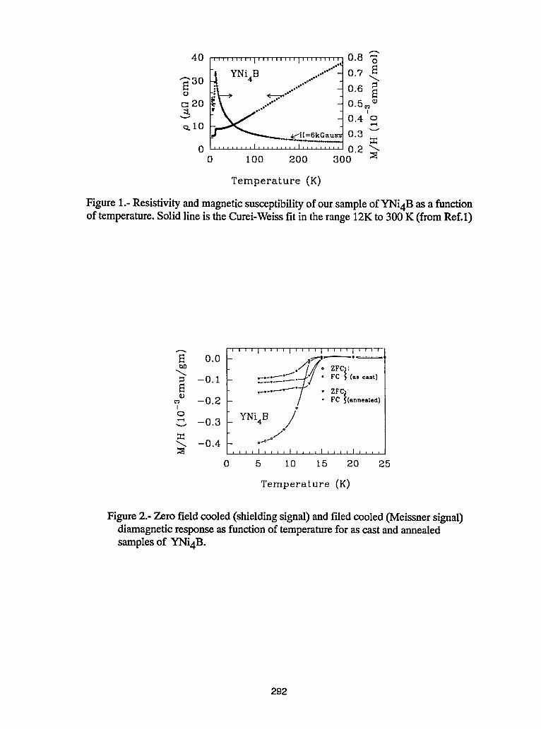
40 0 8 "II1111111 " 0
"-_-30 YNi4B 0.7E 0.6 _
20 ......" 0.5_ _::L ,"-" 0.4 o
Q.I0 _ 0.30 ......... _......... _......... 0.2
0 100 200 300 :_
Temperature (K)
Figure 1.- Resistivity and magnetic susceptibilityof our sample of YNi4B as a functionof temperature. Solid line is the Curei-Weissfit in the range 12K to 300 K (from Ref.1)
,,,,I ,,,,I,,,,i,,,,I,,,,
o.o - --,_'2 ....- .////. zr'c,;
....._'7 " zrg:(D / • FC _(annealed)-0.2
I .
o YNi4 B /"-' -0.3v
_ -o.4_:_ , , , , I , , , , I , , , , I , , , , I , z , ,
0 5 IO 15 20 25
Temperature (K)
Figure2.- Zero field cooled (shielding signal)and filed cooled 0Vleissnersignal)diamagnetic response as function of temperaturefor as cast and annealedsamples of YNi4B.
292
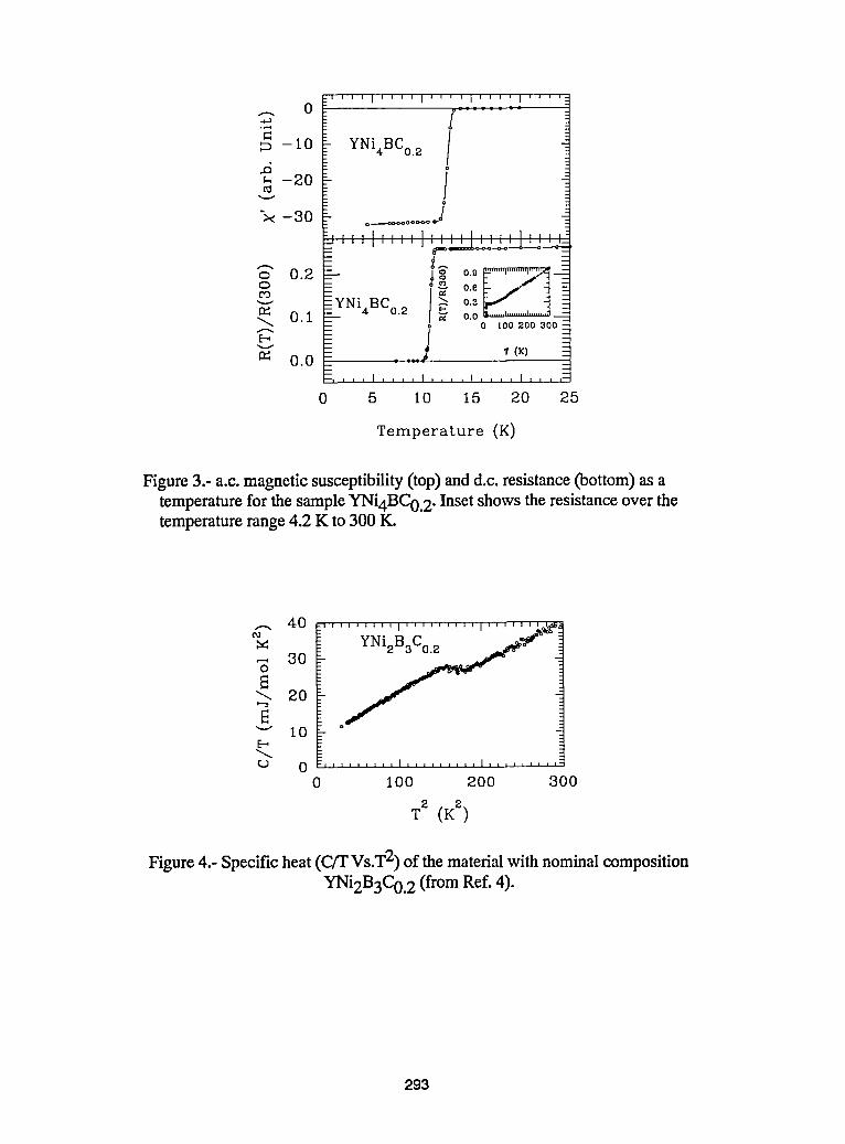
:''''1 .... I .... I .... I ....O o" : : : :" 7" ::
°,...i
° /- 10 YNi4BCo. 2.5 o
_ -20 ]
-_ -30 ....... ]_t',',',',: ',',',',.... ' .... ' .... ;_ ,8_.._.._,_;.,-_--. '__.'__-"- _ --
"o" 0.2 -- _oo 0.g.........J.........,......--_ 0.6
.-_ YNi4BCo. 2 _. o._0.1 - _ 0.0 - '"'"'
o 0 lO0 200 300 --
0.0 .... # T (x)-, , , , I .... I .... I .... I .... "-
0 5 lO 15 20 25
Temperature (K)
Figure 3.- a.c. magnetic susceptibility (top) and d.c.resistance (bottom) as atemperature for the sampleYNi4BC0.2. Inset shows the resistance over thetemperature range 4.2 K to 300 K.
40 -i i I I I I I I I I I II I I II II I I I I II II II_
_ 30 "o
20
o_'_ 10
0 ,,I, ..... I ......... I .........
0 100 200 100
2T (K2)
Figure 4.- Specific heat (C/TVs.T2) of the material with nominal compositionYNi2B3C0.2 (from Ref. 4).
293
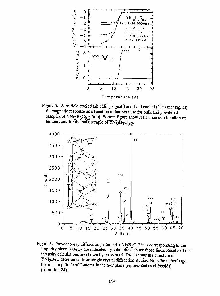
0 .......... I ......... I ....
_ -i YNizBa o2
_ --2 _ Ext. Field 65Gausso_ --3 _' ° ZFC-bulk' -'J • re-bulk
--4 --_"_¢--- 2/ • ZFC-powder
_;_ --5 _ FC powder
-.o _ o =
_ 2°,.,,q
YNi B C2 3 0.2
_ o
E-,{] : : :; •
.... I,,,,I,,,,I,,,,I,,,,
0 5 IO 15 20 25
Temperature (K)
Figure 5.- Zero field cooled (shieldingsignal ) and field cooled (Meissner signal)diamagnetic response as a function of temperature for bulk and powderedsamples of YNi2B3C0.2 (top). Bottom figureshow resistance as a function oftemperature for the bulk sample of YNi2B3C0.2.
4.000 ×
00025OO _ _!Q
2000 lol
1500 ._
200 116 11000 ×105 i 204215
500 002 .- o, • - _211111111111 IIIIll lllilllllll I"T_I I I I_1_1 II llll Illil I I I
0 5 10 15 20 25 30 35 40 45 50 55 60 65 702 theta
Figure 6.- Powder x-ray diffractionpattem of YNi2B2C.Lines correspondingto theimpurityphase "YB2C2 are indicatedby solid circleabove those lines. Results of ourintensitycalculations are shown by crossmark. Inset shows the structureof
YNi2B2C determinedfrom single crystaldiffractionstudies. Note therather largethermal amplitudeof C-atomsin theY-Cplane (representedas ellipsoids)(from Ref. 24).
294
ii iiiIiiiiiiiiii i_1111111 iitl,'- 0.00 .... = = •
-o , ,FC- n
Bulk /I"- • ZFC, FC-Ann /I
---:1- O.01 ..... "'/ Ym2B=C --
_!o--o_--o
-0.02 ,,, ;--,,, ! ......... _........0 10 20 30
Temperature (K)
Figure 7.- Zero field cooled (shielding signal)and field cooled (Meissner signal)diamagnetic response as a function of temperaturefor bulk and powdered samplesof annealed YNi2B2C.The solid lines are guide to the eye.
_11111111111111111111111111111111111-20 -
15 . _ • HoNizB2Co
i0 "
j._ . ErNisBzC
q,%
z ! ,o
/0 .... I .... I .... I , ,
0 5 i0 15
Temperature (K)
Figure 8.- Specific heat ((2)of ErNi2B2C and HoNi2B2C as a function of temperature.The large peaks are due to magnetic ordering in thesematerials In ErNi2B2C, theanomaly due to SC is seen just below 10 K. In the case of HoZNi2B2C2 it is belowthe limit of our observations.
295
' ' ' ' I ' ' ' ' I ' ' ' ' ' ' ' -
.-.looo _.;_ .oNi_B_c-:I\ 711 o 5kGauss
i°°'-''"
ia_i! • 2kGauss500 _ • IkGauss
- 500Gauss-. 200Gauss• OGauss
0 .... I .... I .... I ....0 .5 i0 15 20
Temperature (K)
Figure 9.- Resistance as a function of temperature at various externally applied fields ofHoNi2B2C. Note the doublereentrantbehavior for fields upto 1 KG.
''''1''''I .... I''''I''''I''''I''''
YPd4/3C0.0 /;,_
_0H 0.0 o ZFCl_ _--"/._--to.
o '/g I I 1? /
-_.o / _.°o......._'o;o_'o""Ext. Field 20G T (K)
r i f ii , , , , t . , . . I . . ,. I , , , , I i i i i I .., .
0 5 I0 15 20 25 30 35
Temperature (K)
Figure 10.-Zero field cooled (shieldingsignal) and field cooled (Meissner signal)diamagnetic response as a function of temperature for material of nominalcomposition YPd4BC0.5. Solid lines areguide to the eye. Inset shows resistance (r)of the sample as a function of temperature (from Ref. 8). Note two superconductingtransitions.
296
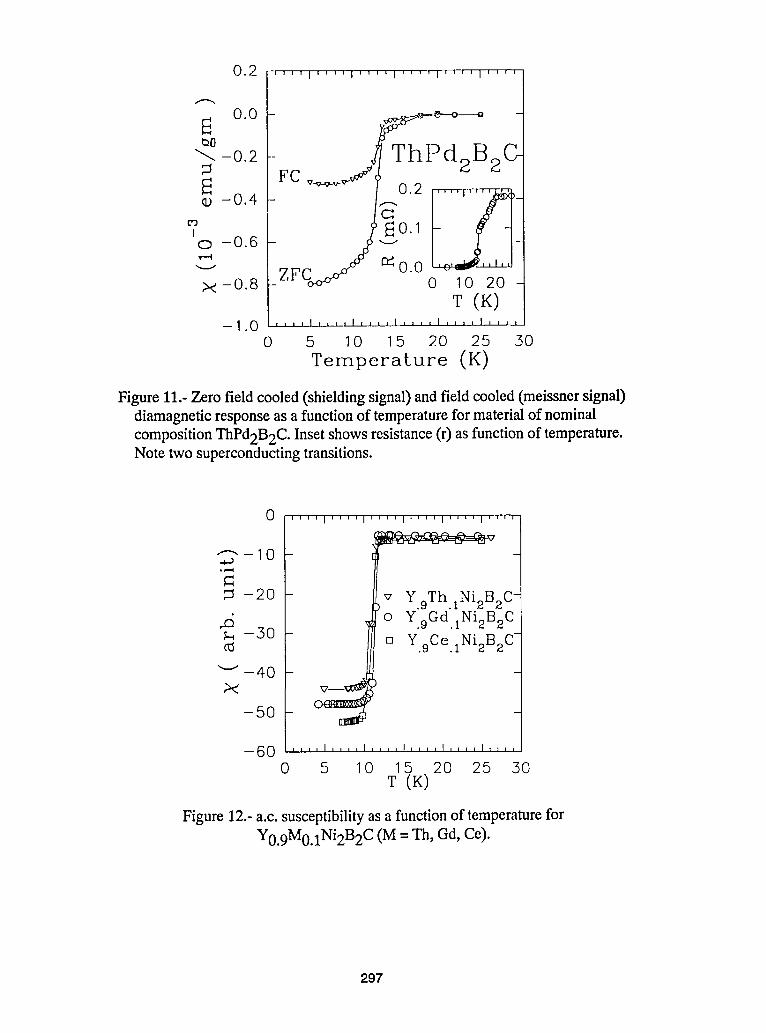
0.2 ' ' ' ' I ' ' ' ' I ' ' ' ' I ' ' ' ' I ' ' ' ' I ' ' ' '
o.o-
ThPd2B CFC __, 20.2
o -0.4 -
,,,_,_ _ i+1+ rll ii
' _0.1O -0.6 _"
I_o. 0;:_-0.8 ZF 0 10 20 -
T (K)--1 . 0 .... I .... I .... I .... I .... + .....
0 5 10 15 20 25 30TemperaLure (K)
Figure 11.- Zero field cooled (shieldingsignal) and field cooled (meissnersignal)diamagnetic response as a function of temperaturefor material of nominalcomposition ThPd2B2C. Inset shows resistance (r) as functionof temperature.Note two superconducting transitions.
0 ''''1 .... ''''1''''1''''1''''
_-10 -.,-=1
• I
-20- v Y.9Th.lN12B2C-,£_ o Y 9Gd INi2BzC
_-50 - [] Y'9Ce" NizB2C-. .
-40 -X v
-50 - _
--60 .... I .... I , i , , I .... I .... I , , , ,
0 5 10 15 20 25 50T (K)
Figure 12.-a.c. susceptibility as a function of temperature forY0.9M0.1Ni2B2C (M = Th, Gd, Ce).
297
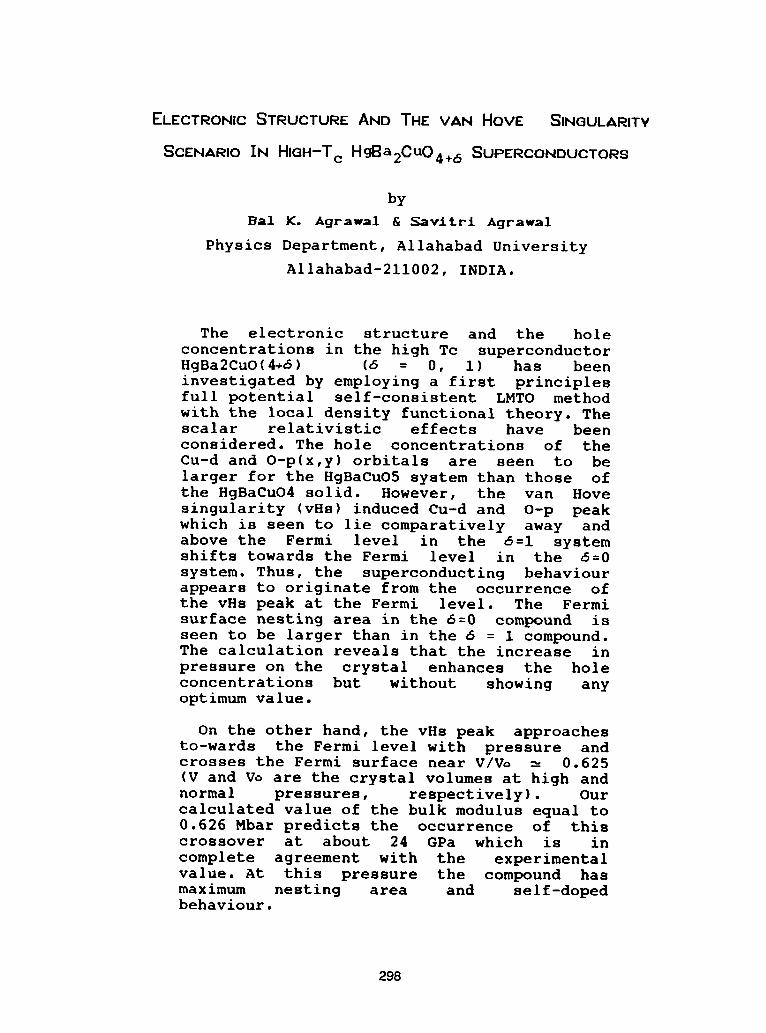
ELECTRONIC STRUCTURE AND THE VAN HOVE SINGULARITY
SCENARIO IN HIGH-T c HgBa2Cu04+ 6 SUPERCONDUCTORS
by
Bal K. Agrawal & savltri Agrawal
Physics Department, Allahabad University
Allahabad-211002, INDIA.
The electronic structure and the holeconcentrations in the high Tc superconductorHgBa2CuO(4+6) (6 = 0, i) has beeninvestigated by employing a first principlesfull potential self-consistent LMTO methodwith the local density functional theory. Thescalar relativistic effects have beenconsidered. The hole concentrations of theCu-d and O-p(x,y) orbitals are seen to belarger for the HgBaCuO5 system than those ofthe HgBaCuO4 solid. However, the van Hovesingularity (vHs) induced Cu-d and O-p peakwhich is seen to lie comparatively away andabove the Fermi level in the 6=1 systemshifts towards the Fermi level in the 6=0system. Thus, the superconducting behaviourappears to originate from the occurrence ofthe vHs peak at the Fermi level. The Fermisurface nesting area in the 6=0 compound isseen to be larger than in the 6 = 1 compound.The calculation reveals that the increase inpressure on the crystal enhances the holeconcentrations but without showing anyoptimum value.
On the other hand, the vHs peak approachesto-wards the Fermi level with pressure andcrosses the Fermi surface near V/Vo _ 0.625(V and Vo are the crystal volumes at high andnormal pressures, respectively). Ourcalculated value of the bulk modulus equal to0.626 Mbar predicts the occurrence of thiscrossover at about 24 GPa which is incomplete agreement with the experimentalvalue. At this pressure the compound hasmaximum nesting area and self-dopedbehaviour.
298
I.INTRODUCTION :
The compound HgBa2CuO(4+6) ( 6 = 0, i) has beenseen [i] to be superconducting with Tc=94°K.Schilling et al [2] have observed a Tc=I33°K in amaterial containing HgBa2Ca2Cu30(8+6) andHgBa2CaCu20(6+6). Quite recently, values of Tc% ashigh as 164°K at high pressure have been reported inHgBa2Ca2Cu30(8+6) samples [3,4].
In understanding the cause of the occurrence ofsuperconductivity in high Tc superconductors, one cannot ignore the crucial role played by the CuO2planes. In two-dimensions, one come across with thesaddle points at symmetric points of the Brillouinzone which lead to logarthimic vHs in the electrondensity of states obtained even after assuming onlynearest-neighbour hopping. It has been seen [5] thata simple reformulation of BCS theory in the weakcoupling limit considering the occurrence of a vHsnear the Fermi energy may lead to quantitativelydifferent results. The value of Tc may be much higherachieving its maximum value when the van Hovesingularity coincides with the Fermi energy.
In the present communication, we investigatethe occurrence of the van Hove singularity in theHg-based single CuO2 layer compounds HgBa2CuO(4+6)(6=0,1). Novikov and Freeman [6] and Rodriguez et al[7] have also performed a LMTO calculation for the6=0 compound but have not investigated the pressureeffects. Our similar results for HgBa2CaCu20(6+6)(6=0,1) have been reported elsewhere [8]. The presentLMTO method goes beyound the usually employed LMTOmethod in the atomic sphere approximation which hasseveral limitations. The method is seen to predictthe electronic structure, lattice constants, elasticconstants, and phonon frequencies, for the simplesystems III-V and II-VI semiconducting compounds likeAIAs, CdTe, GaSh, ZnSe, ZnTe, ZnS etc [9]. Also, theparent compound CaCuO2 of the recently discoveredhigh Tc oxide superconductors has been successfullystudied [10].
II.CALCULATION AND RESULTS
The crystal structures of HgBa2CuO(4+6) (6=0,1)possess the space group P4/mmm. The latticeparameters of the tetragonal cell are theexperimentally measured values i.e., a=3.8797 A° andc=9.509 A°. In HgBa2CuO5, the atomic positions in theunit cell are Cu:(0,0,0); O(i) :(0.5a,0,0);O(2):(0,0.5a,0); Ba:(0.Sa,0.5a,+0.294c);
299
O(3):(0,0,_0.294c); Hg:(0,0,0.5c) and
O(4):(.5a,.5a,.5c). For HgBa2CuO4, the atom 0(4) ofthe HgO plane has been removed.
The basis functions with IS 4 and of energies-0.01, -I.0 and -2.3 Ry were chosen for making theexpansions of the products of the LMTO envelops. _hedecays of these functions were taken as _2=-I and -3Ry. Each atomic sphere has thus 50 functions. Thelocal density potential of Hedin and Lundquist [ii]has been utilized. A spd basis each for the two highenergies -1.0 and -0.01 Ry and a sp basis for theenergy -2.3 Ry were employed for every real atom. Itleads to a number 22 of LMTO's per atom.
The muffin-tin (MT) spheres chosen to fill thespace were slightly non-overlapping. The radii ofthese atomic spheres in atomic units were Cu(2.0),O(1.655), Ba(3.35) and Hg(2.05).
The valence states considered for the variousatoms are Cu(3d,4s,4p); O(2s,2p,3d); Ba(6s,6p,5d) andHg(6s,6p,6d). The core electrons are treated not in afrozen-core approximation but are allowed to relax.A number of 72 k-points obtained by the samplingmethod in the irreducible part of the Brillouin zonewere employed in all the calculations. The 6=0compound shows minimum in the crystal energy at avolume ratio (V/Vo)=l.05, where Vo is theexperimental crystal volume for the 6 = 0.1 sample.Novikov and Freeman [6] and Rodriguez et al [7] havereported results for a different set of valencestates.
(i) ELECTRONIC STRUCTURE :
The dispersion curves for a number ofsymmetry points lying in the two different k(x,y)planes have been depicted in Fig.l. They are F =(0,0,0); X = (H/a)(l,0,0); M = (n/a)(l,l,0); Z =(H/a)(0,0,a/c); R = H(I/a,0,1/c) and A =H(i/a,i/a,i/c). The origin of the energy is taken atFermi level (Ew).
The electronic structure is very muchtwo-dimensional. The dispersion of the valence bandsalong the c-axis i.e., along the symmetry directionF-Z is quite small. The band structure in the twodifferent planes along k= are very much similar.
In Figs. ib, ic and id, we have alsodepicted those parts of the dispersion curves forwhich the probability of any wave function on an atom
300
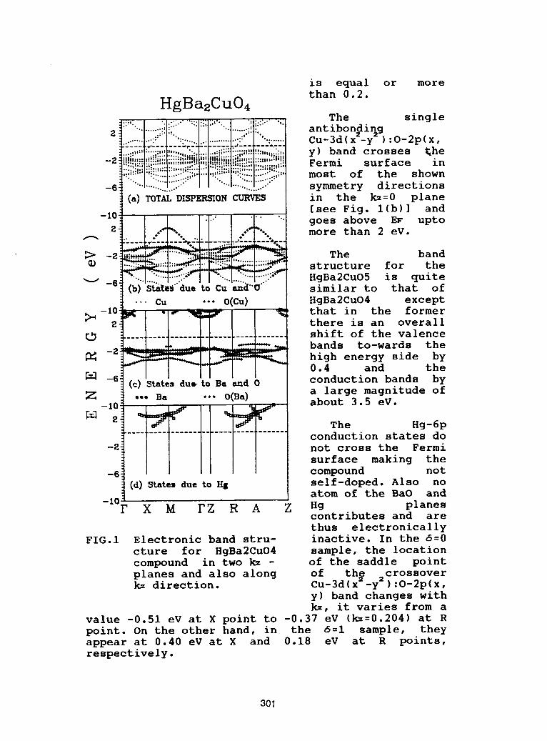
is equal or morethan 0.2.
HgBa2Cu04The single
_,.. ".i[_.'"'::: :::""';;2 ......:_!I _. antibonding.. .. • x2_y=).......::- ,::................._-......'..:.__.......Cu-3d( :O-2p(x,.............-- _he
..,......._....... .:...[.--.:......,,...::y) band crosses. _ ..... Fermi surface in•. ,":......; :::_F"";:"::_!::'_::::'"'_......;_I':'"':- most of the shown......"....• .. symmetry directions(a)TOTALDISPER_ONCURVES in the kz=0 plane
[see Fig. l(b)] and
2 N _: % more than 2 eV._ -2 _ _ _ " The band
""-.I.///_"'[3::__ ............._ structure for the....[[.._.3[:..-HgBa2CuO5 is quite-6 (b)StA_"due Cu ariZ"O" similar to that of
•.. Cu .-.O(Cu) HgBa2CuO4 except
_-I0 _ --* _ _ II-- _ that in the former
2 _ _ _-I__ii i __ there is an overall
[._ .............. shift of the valencebands to-wards the
-2 _ _ ___ high energy side by0.4 and the
_/ -6 (c)_tate,du_to|||Ba,nd0 conduction bands bya large magnitude ofZ ,..Ha ...O(Ba) about 3.5 eV.
2 ' The Hg-6p.................................conduction states do
-z not cross the Fermisurface making the
-6 compound not(d)Sta%esdue%oHIK self-doped. Also noatom of the BaO and
-IOF X I_ FZ R A Z Hg planescontributes and arethus electronically
FIG.I Electronic band stru- inactive. In the 6=0cture for HgBa2CuO4 sample, the locationcompound in two kz - of the saddle pointplanes and also along of the 2crossoverk= direction. Cu-3d(x2-y ):O-2p(x,
y) band changes withk_, it varies from a
value -0.51 eV at X point to -0.37 eV (k==0.204) at Rpoint. On the other hand, in the 6=1 sample, theyappear at 0.40 eV at X and 0.18 eV at R points,respectively.
301
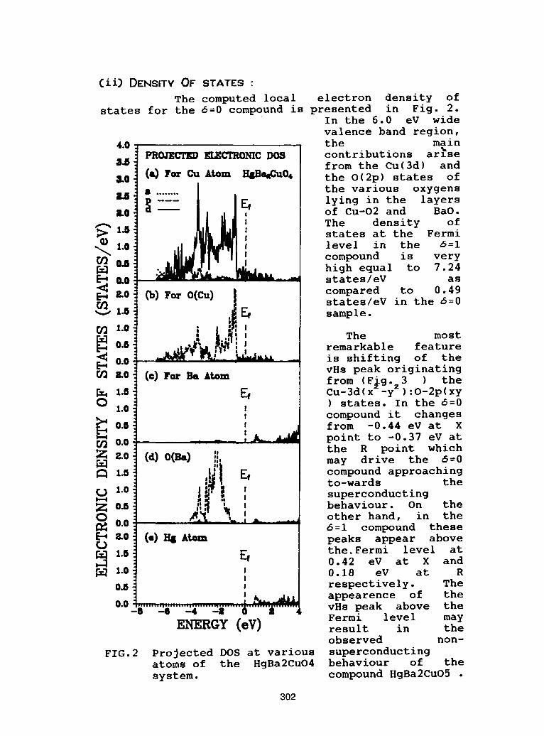
(ii) DENSITY OF STATES :
The computed local electron density ofstates for the 6=0 compound is presented in Fig. 2.
In the 6.0 eV widevalence band region,
4.0 the mainPRO/ECTEDELECTRO_CD08 contributions arlse
from the Cu(3d) and_0 (4 For _ A_m HIBa_u_ the O(2p) state• of
U • ........ the various oxygens
&0 _ --- Ef lying in the layers, of Cu-O2 and BaO.l The density of
_ 1_ ! states at the Fermi
_ 1.0 ! level in the 6=1! compound is very
high equal to 7.24
•0 states/eV as_0 _) For O(Cu) compared to 0.49states/eV in the 6=0_1_ _ •ample.
0'] 1.0 |• l The mostO_ I remarkable feature
0.0 is shifting of theC/_LO (©)For Ba A_m vHs peak originating
from (F&g.23 ) the1.5 _ Cu-3d(x -y ):O-2p(xy
O ) states. In the 6=01.0! compound it changes
0.5 !_ from -0.44 eV at X0.0 _ point to -0.37 eV at
_0 (d)O(Ba) " the R point which_ may drive the 6=0' compound approaching
_:_I_ _ to-ward• the
1.0 _ _ superconductingO_ O_ behaviour. On the0.0 .! ___ other hand, in the6=1 compound these•0 (o)HIAtmn peak• appear above
_ 1.5 _ the_Fermi level at0.42 eV at X and
1.0 0.18 eV at RlO_ l respectively. The
I _,L....,ILl appearence of the0.0__....../_....../_.....Ti......i_.._...._.......i vHs peak above the
ENERGY(eV) Fermi level mayresult in theobserved non-
FIG.2 Projected DOS at various superconductingatoms of the HgBa2CuO4 behaviour of thesystem, compound HgBa2CuO5 •
302
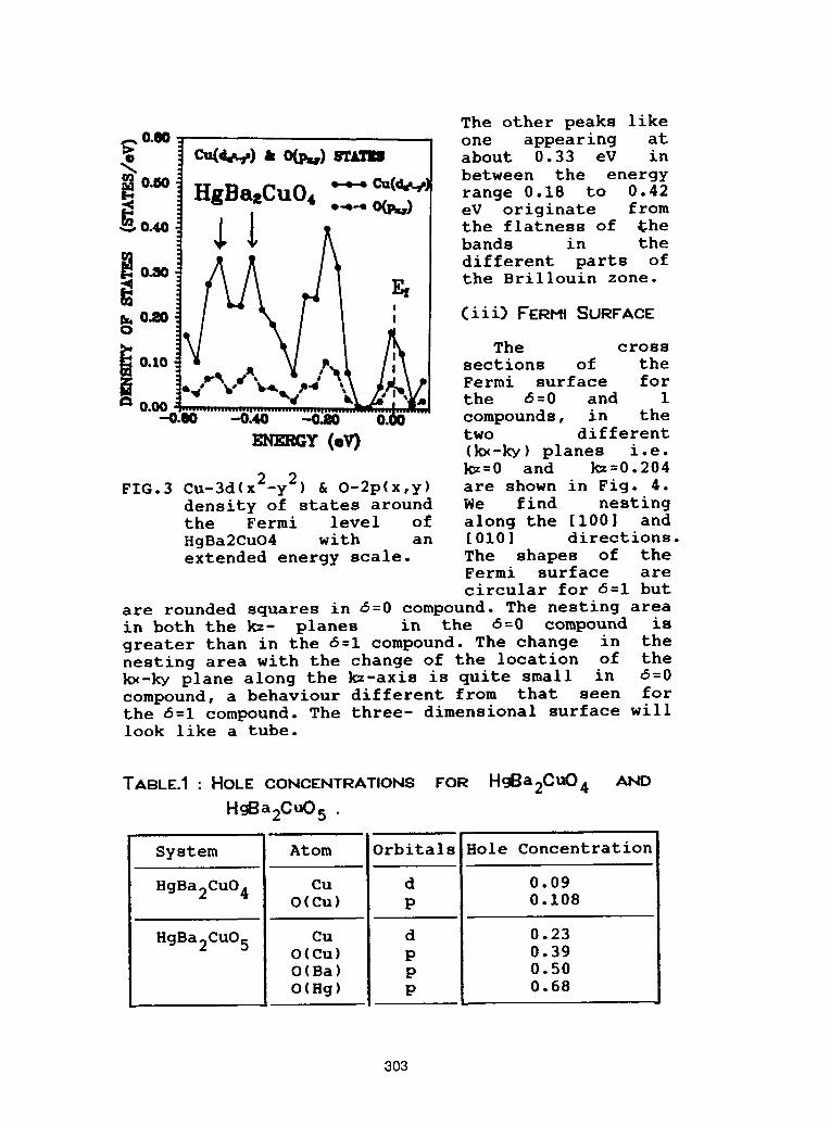
The other peaks like
0.e0 one appearing atC_) &O_w) STATES about 0.33 eV in
between the energyO5O HgBa,Cu04_ Cu(d_) range 0.18 to 0.42
• _ ._-.O_) eV originate from_0.40 _ the flatness of _he
bands in the
different parts of
0..50 the Brillouin zone.
!0.20 , (iii) FERMI SURFACE
O
The cross
sections of the0.10 T% w_ Fermi surface for
O.00 the 6=0 and 1-0.40 compounds, in the
ENERGY (e_ two different(kx-ky)planes i.e.k_=0 and kz=0.204
FIG.3 Cu-3d(x2-y2) & O-2p(x,y) are shown in Fig. 4.density of states around We find nestingthe Fermi level of along the [i00] andHgBa2CuO4 with an [010] directions.extended energy scale. The shapes of the
Fermi surface arecircular for 6=1 but
are rounded squares in 6=0 compound. The nesting areain both the k=- planes in the 6=0 compound isgreater than in the 6=1 compound. The change in thenesting area with the change of the location of thekx-ky plane along the kz-axis is quite small in 6=0compound, a behaviour different from that seen forthe 6=1 compound. The three- dimensional surface willlook like a tube.
TABLE.l: HOLE CONCENTRATIONS FOR HgBa2CuO 4 AND
HgSa2CuO5 .
System Atom Orbitals Bole Concentration
HgBa2CuO4 Cu d 0.09O(Cu) p 0.108
HgBa2CuO5 Cu d 0.23O(Cu) p 0.39O(Ba) p 0.50O(Hg) p 0.68
303
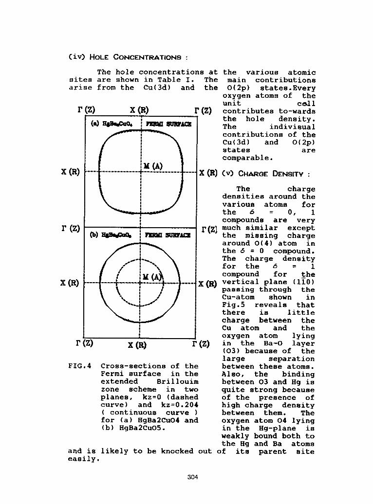
(iv) HOLE CONCENTRATIONS :
The hole concentrations at the various atomicsites are shown in Table I. The main contributionsarise from the Cu(3d) and the O(2p) states.Every
oxygen atoms of theunit cecil
F (Z) X (R) F (Z) contributes to-wards
(___ ; the hole density.:FER_I_ The indivisualcontributions of theCu(3d) and O(2p)states arecomparable.
=M(A)X (R) X (R)(v) CHARGE DENSITY :
The chargedensities around thevarious atoms forthe 6 = 0, 1compounds are very
F (Z) _) _ FERMISURF_ F(Z] much similar exceptthe missing chargearound 0(4) atom inthe 6 = 0 compound.The charge densityfor the 6 = 1
]M compound for theX (R) X (R) vertical plane (II0)
passing through theCu-atom shown inFig.5 reveals thatthere is littlecharge between the
!, Cu atom and the!
I oxygen atom lying
F (Z) X (R) F (Z) in the Ba-O layer(03) because of thelarge separation
FIG.4 Cross-sections of the between these atoms.Fermi surface in the Also, the bindingextended Brillouim between 03 and Hg iszone scheme in two quite strong becauseplanes, kz=0 (dashed of the presence ofcurve) and kz=0.204 high charge density( continuous curve ) between them. Thefor (a) HgBa2CuO4 and oxygen atom 04 lying(b) HgBa2CuOb. in the Hg-plane is
weakly bound both tothe Hg and Ba atoms
and is likely to be knocked out of its parent siteeasily.
304
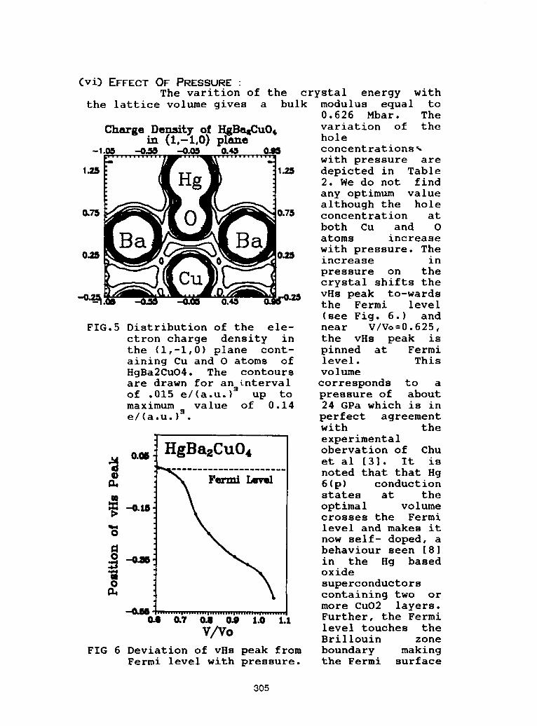
(vi) EFFECT OF PRESSURE :The varition of the crystal energy with
the lattice volume gives a bulk modulus equal to0.626 Mbar. Thevariation of the6"_arse Density of __ BaaCu04
in(I,-1,0)plexe hole-I. -O_ -0.06 _45 _ concentrations%
with pressure are1.2.5 1.26 depicted in Table
2. We do not findany optimum valuealthough the hole
•_ 0._ concentration atboth Cu and Oatoms increasewith pressure. The
0_ 025 increase inpressure on thecrystal shifts thevHs peak to-wards
"_-- 0.46 the Fermi level(see Fig. 6.) and
FIG.5 Distribution of the ele- near V/Vo=0.625,ctron charge density in the vHs peak isthe (i,-I,0) plane cont- pinned at Fermiaining Cu and O atoms of level. ThisHgBa2CuO4. The contours volumeare drawn for an Lnterval corresponds to aof .015 e/(a.u.)s up to pressure of aboutmaximum value of 0.14 24 GPa which is ine/(a.u.)s. perfect agreement
with theexperimental
H_Ba2CuO4_ obervation of ChuO.O8
et al [3]. It isnoted that that Hg6(p) conductionstates at the
_ optimalvolume
crosses the Fermi
level and makes itnow self- doped, a
behaviour seen [8]_ in the Hg based
oxidesuperconductorscontaining two or
................................................more CuO2 layers.•7 _8 U I_ 1.1 Further, the Fermi
_/VO level touches theBrillouin zoneFIG 6 Deviation of vHs peak from boundary making
Fermi level with pressure, the Fermi surface
3O5
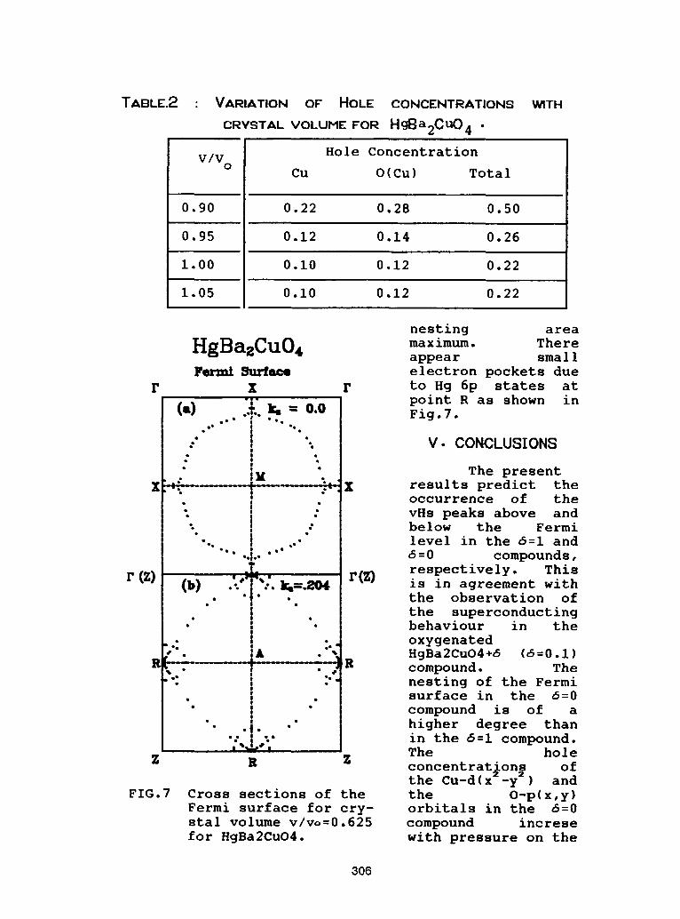
TABLE.2 : VARIATION OF HOLE CONCENTRATIONS WITH
CRYgTAL VOLUME FOR HgBa2CuO 4 •
Hole ConcentrationV/V
oCu O(Cu) Total
0.90 0.22 0.28 0.50
0.95 0.12 0.14 0.26
1.00 0.i0 0.12 0.22
1.05 0.i0 0.12 0.22
nesting area
HgB maximum. Therea2Cu04 appear smaI1FenI_ Surface electron pockets due
r x r to Hg 6p states at_._ point R as shown in
(,) "..:..= 0.0 Fig.7••le o •
.• | Qe
" _ "" " V CONCLUSIONS: t :
• I • The present!MX _::[ | .:_X results predict the" occurrence of the
" ' : vHs peaks above and• i • below the Fermie | •
"-.. _ ..'" level in the 6:1 and-o. _ Q.e•.,.. 6=0 compounds,
respectively. This.'..oT,;.r(z)r (Z) (b) k,=._)4 is in agreement with
•• "_" --_ the observation ofthe superconducting
• • behaviour in the• oxygenated"'. 8A •:'_ HgBa2Cu04+6 (6=0.i)
R - R compound The• • .d "e• •• • nesting of the Fermi. surface in the 6=0• " compound is of a". •" higher degree than• •
.0 O .O
:,JL*; in the 6=i compound.The holeZ R Z concentrations of
the Cu-d (x2-y2) andFIG.7 Cross sections of the the O-p(x,y)
Fermi surface for cry- orbitals in the 6=0stal volume v/vo=0.625 compound incresefor HgBa2CuO4. with pressure on the
306
crystal. The deviation of the vHs peak from theFermi level also decreases with the pressure on thecrystal and the vHs is pinned at Fermi level at apressure of about 24 GPa in perfect agreement withexperimental data. The nesting area of the Fermisurface is also maximum at this optimum value.
VI ACKNOWLEDGEMENTS
The present work is financially supported byUniversity Grants Commission, New Delhi andDepartment of Science and Technology, New Delhi.
REFERENCES
I. S. N. Putilin, E.V. Antipov, O. Chmaissem and M.Marezio, Nature, 362, 226(1993).
2. A. Schilling, M. Cantoni, J D Guo and H. R. Ott,Nature, B363, 56(1993).
3. C.W. Chu et al Nature, 365, 323 (1993).
4. H. Takahasi et al Physica C 218 , 1 ( 1993 ).
5. J. Labbe, and J. Bok ,Europhys, Lett., 5,1225(1987), D. M. Newns, C.C. Tsuei, P. C.Pattnaik and C.L. Kane, Comments Condens., MatterPhys. 15, 273(1992); H. R. Krishnaswamy et alPhys. Rev., B49, 3520 (1994).
6. D.L. Novikov and A.J. Freeman Physica C 212, 233(1993).
7. C.O. Rodriguez et al, Physica 2!6,12, (1993).
8. Bal K. Agrawal & Savitri Agrawal, High Tc-updateMay i, 1994.
9. Bal K. Agrawal & Savitri Agrawal, Phys. Rev B45,8321(1992); and also preprint.
i0. Bal K Agrawal & Savitri Agrawal, Phys. Rev. BI,in press.
ii. L. Hedin and B.I. Lundquist, J.Phys., C4, 2063(1971).
307
BOSON LOCALIZATION AND UNIVERSALITYIN YBa_Cu3-xMxO_-5
A. Kallio,V. Apaja and S.PSykkiiUniversity of Oulu, Department of Theoretical Physics, Linnanmaa, 5F-90570 Oulu, Finland
(June 22, 1994)
Abstract
Weconsidera twocomponentmixtureof chargedfermionson neutralizingback-groundwith all sign combinationsand arbitrarilysmall mass ratios. In the twoimpurity limit for the heavier componentwe show that the pair forms a boundstate forall charge combinations. In the lowest orderapproximationwe derivea dosed formexpressionVeyl(r) for the bindingpotential which has short-rangerepulsionfollowedby attraction. In the classicallimit, when the mass of embed-ded particles is large ms >> m, we can calculate fromVel](r) also the cohesiveenergyE and the bondlength R of a metalliccrystalsuch as lithium. The lowestorderresult is R = 3.1It,, E -- -.9 eV, not entirelydifferentfrom the experimen-tal result forlithium metal. The same interaction for two holes on a parabolicband with ms > m gives the quantum mechanicalbound state which one mayinterpreteas a bosonor local pairin thecase ofhigh-Toand heavyfermionsuper-conductors.We also show that forcompoundsof the type YBa2Cu3-zMzOT-6one can understandmostof the experimentalresults for the superconductingandnormalstates with a single temperaturedependentboson breakingfunction f(T)for each impuritycontent z governingthe decayof bosonsinto pairing fermions.In the normal state f(T) turnsout to be a linear, universalfunction, independentof the impurity content z and the oxygencontent & Wepredictwith universalitya depressionin T¢(z) with slightdownbendingin agreementwith experiment. Asa natural consequenceof the modelthe bosonsbecomelocalizedslightly aboveT_due to the Wignercryst_ll;,ation, enhancedwith lattice local fieldminima. Theholes remaindelocalizedwith a linearlyincreasingconcentration in the normals-tate, thus explainingthe risingHalldensity.The bosonlocalizationtemperatureTBL shows up as a minimumin the Hall density Ra-_. We also give explana-tion forvery recently observedscaling of temperaturedependent Halleffect inLa2-xSrxCuO4.
I. INTRODUCTION
Despite great efforts, high-To superconductivity HTS is still lacking a convincing theoreticalexplanation that everybody can accept. There is ample experimental evidence for high-To,heavy fermions HF and Chevrel compounds that the properties of these systems cannot beunderstood with the most simple BCS model alone. More than anything the normal stateproperties in all these compounds deviate from BCS, which above the transition temperatureTc would predict a normal metal. The anomalies appear in the three main experiments: theNMR, the Raman and Hall experiments and to some extent in the thermal conductivity andsurface resistivity.
The Hall-density (nil = 1/Rec) in the ab-plane is diminishing just above Tc and showsa minimum at TBL _> Tc and beyond the minimum it rises linearly. In the case of 123 theHall coefficients in different direction have opposite signs Rab _> O, Rc <_ 0 [1]. This, morethan anything, requires existence of charge carriers of more than one type in these compounds.Furthermore the NMR relaxation rate W(T) below Tc does not show a shoulder predicted by
308
BCS. At very low temperatures the relaxation rate W(T) exhibits power laws with very smallexponent like 1.5 as compared with exponential BCS-behaviour or linear Korringa-behaviour[2]. The Korringa law is not obeyed in the normal states. The Raman scattering shows nocoherence peak at w -- 2A hut continuum background [3], unexplainable within the BCS.
Inthecaseof123-compoundsalltheanomaliesmentionedabovecan beunderstoodintermsofdoublychargedboson model wherethebosonsexistup totemperatureTB _ 300- 500 K,
much higherthan To. Below thistemperaturethe bosonsare inchemicalequilibriumwithrespecttoreactionB ++ _ h+ + h+,where theholesaresupposedtobe tiedtoa band withparabolicdispersionrelation.The chemicalequilibriumcan quitegenerallybe representedbya bosonbreakingfunctionf(T)suchthatthenumber densityofbosonsand fermionsare
nB(T)----no/(T)nh(T) = 2no [1 -/(T)], (1)
which simply contains the charge conservation. Just like dissociation in chemistry takes placein a solvent, here the equilibrium reaction takes place in the sea of electrons.
From the Hall-experiments we have deduced that f(T) is nearly linear function above Tc[4]. If the bosons and holes are tied to the ab-plane they both contribute to Hall-density andRab > 0. The minimum in the Hall-density is explained by the Wigner crystallization (andhence by localization) of bosons above a temperature TBL > To, since their density gets smallerthan the critical density for Wigner crystallization. Similarly near T = 0 the density of the holesgets small since l-f (T) --* O. The model therefore predicts antiferromagnetic transitions in thesuperconducting states. Such transitions are also often observed. Although we cannot claimthat they all are connected with the proposed Wigner crystallization of the pairing fermions,it is di_cult to understand why they occur near T -- 0. In c-direction the Hall density isdominated by the background electrons, called spectators.
The plan of the paper is as follows: First we show that the existence of bosons is feasible.In fact we will calculate the relative wave function of such boson and its binding energy in thecase of two charged particles with heavy mass embedded in the electron gas with neutralizingbackground. We do this by applying the hypernetted chain (HNC) method of classical statisticalmechanics which has previously been shown to be very accurate for electron gas. In chapter IIIwe consider boson localization and in chapter IV two types of universal behaviour in high-Tosuperconductors.
II.SPECTATOR FERMION BINDING OF BOSONS
To introduce the method we repeat the steps needed to calculate energy/particle of theelectron gas. Here the relevant density parameter is the rs-value defined by the volume takenby one electron n -1 = 47r(rsa0) 3, where a0 is Bohr radius = li2/me 2. Another relevant quantityis the radial distribution function g(r12) which gives the relative probability of finding an otherelectron at the position r2, if there is one at the point rl. For uniform electron liquid g(rl_)is independent of the angles r12. The corresponding probability amplitude _b(r12) is ,vi_r12).With Coulomb interaction vc(r) the potential energy can be calculated exactly form
V 1-- - -n ig(r)-1lYe(r), (2)N 2
providedthatfunctiong(r)iscalculatedfromtheexactgroundstatewavefunction€ by
.,f 1912dr_n2g(r12) = N(N - i) f i¢l_dr, (3)
where N is number of particles and dv = d3rld3r2dT"2 . For interactions other than Coulombforce one has g(r)V(r) inside of the integrand in Eq. (2). The reason for (g - 1)vc is thescreening. Since g(r) --* 1 at large distances, this also makes the integral in Eq. (2) to converge.
Another function which, in the case of quantum liquids, is intimately connected with neutronscattering experiments, is the liquid structure factor S(k) which is obtained by Fourier transformofg(r)- I
309
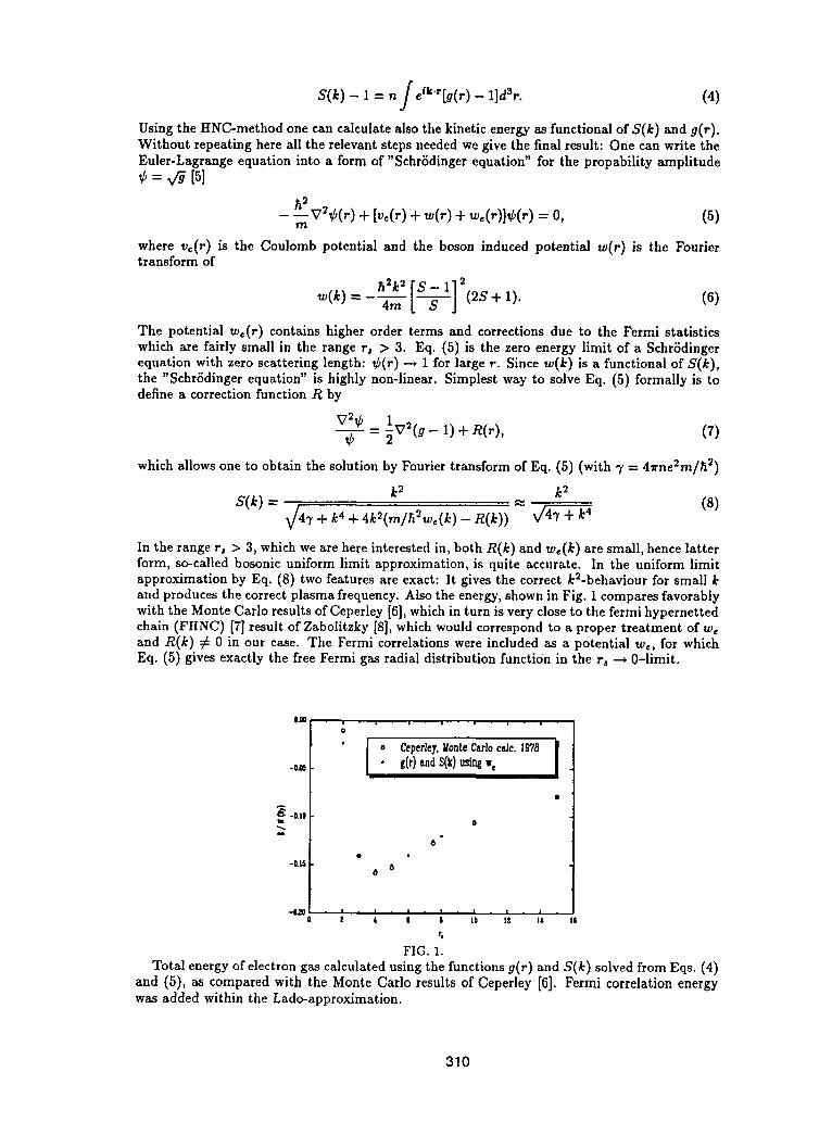
t
S(k) - 1 = n J eik'r[g(r) -- lldZr. (4)
Using the HNC,-method one can calculate also the kinetic energy as functional of S(k) and g(r).Without repeating here all the relevant steps needed we give the final result: One can write theEuler-Lagrange equation into a form of "SchrSdinger equation" for the propability amplitude¢ =v_ [s]
h2- --v2¢cr)+ [v°(r)+ w(r)+ w+Cr)]¢Cr)=0, (5)m
where v¢(r) is the Coulomb potential and the boson induced potential w(r) is the Fouriertransform of
_(k)= - 4--_ (2s+ 1). (6)
The potential we(r) contains higher order terms and corrections due to the Fermi statisticswhich are fairly small in the range r, > 3. Eq. (5) is the zero energy limit of a SchrSdingerequation with zero scattering length: ¢(r) ---*1 for large r. Since w(k) is a functional of S(k),the "Schrgdinger equation" is highly non-linear. Simplest way to solve Eq. (5) formally is todefine a correction function R by
Vs____¢¢=lv2(g- 1)+ n(r), (7)¢
which allows one to obtain the solution by Fourier transform of Eq. (5) (with 7 = 4_rne2m/lis)
ks ksS(k) (8)
_47 + k4 + 4k2(m/liSw,(k) - R(k)) V_ + k"
In the range r, > 3, which we are here interested in, both R(k) and we(k) are small, hence latterform, so-called bosonic uniform limit approximation, is quite accurate. In the uniform limitapproximation by Eq. (8) two features are exact: It gives the correct k2-behaviour for small kand produces the correct plasma frequency. Also the energy, shown in Fig. 1 compares favorablywith the Monte Carlo results of Ceperley [6], which in turn is very close to the fermi hypernettedchain (FHNC) [7] result of Zabolitzky [8], which would correspond to a proper treatment of weand R(k) _ 0 in our case. The Fermi correlations were included as a potential we, for whichEq. (5) gives exactly the free Fermi gas radial distribution function in the r° _ 0-limit.
0_ - i - + - + - | - . - | - i -o
* Ceperley,MonteCarlotale. 197t1 I__ • g(r)andS(k)_ w,
@
_ -ILIO ,..
6@
-0,15 6
• ' - ' " ' + ' - ' , I , f ,-020 l 1 I I tO I! II II
r,
FIG.I.
Totalenergyofelectrongascalculatedusingthefunctionsg(r)and S(k)solvedfromEqs.(4)and (5),as compared withtheMonte CarloresultsofCeperley[6].Fermi correlationenergywas added withintheLado-approximation.
310
The effect of screening comes out in a vivid way from Eq. (5): The free space Coulombinteraction is changed into an effective interaction V_/I = vc + w due to the other electronsaround. In fact for large r, vc is completely cancelled by w(r) and hence Ve!l(r) has finiterange.
With these preliminaries we are ready to examine what happens if we embed charged particlesinto the electron gas. The same treatment with radial distribution functions can be generalizedfor a mixture: One obtains a system of three coupled equations of the type Eq. (5). Calling thesecondcomponentmass m2, densityn2 and chargeQ2 = Ze one would now needthreeradialdistributionfunctionsg11(r)= g(r)(= theelectrongas)g12(r)and g22(r)andthecorresponding
probabilityamplitudesCq = _/_',whichsatisfythefollowingthreecoupledEuler-Lagrangeequations
- --'_72¢_j + + wq eli=O, i,j =1,2 (9)Plj
with I/1 -- m, I/2 = m2 and P12 -- mm2/(m + m2) = m/(1 + M). The detailed expressions forwq are to be found in Ref. [9]. It turns out that the set (9) has again a solution if the massratio M _ 1, but for M < .1 there seems to be no solution numerically [10]. For these reasonit was thought that this approach cannot be applied to a problem like the metallic hydrogen.However, since the method works so well in the single component case, the reason for thisinadequacywas not fullyunderstoodearlier.Our purposehereistoshow thatthereasonfor
instabilityisappearanceofbound stateinchannels¢22or ¢12 whichone simplyhas totreatmore properly.In whatfollowswe willshow thatthepropertreatmentistogofirsttoone andtwo impuritylimitsn2/n ....+0. Inthislimitone obtainsa decouplingofthe threeequations:Firstequationreducestothebackgroundelectrongasdescribedbefore.For theimpurity,one
obtainstheliquidstructurefactorSl2(k)from S(k)oftheelectrongasby
4S2(k) [Z7 1 _] 4Z-yS2(k) (10)S12 - 1 + MS(k) _ + (1 + M) = k4(1 -I-MS(k))
The small correction function R12(r) has analogous meaning as the one in Eq. (7) with thedefinition
V_¢12- 1V2(g,2- I)+ R12(r) (11)
¢12 2
and inallFouriertransformsthebackgroundelectrondensityn isused.For smallmass ratioM _ 0 we obtainintheuniformlimitforbothR -- RI2 --0 verysimpleform
4Z7 (12)$12(k) -- 47 + k4'
showing that the sign of S12 is opposite to charge Q2 = Ze. The third component in this limitdecouples also and we obtain a SchrSdinger equation for the pair
-- --V2_)22 "_ + W22 ,_22 ---- E¢22 (13)rn2
with induced potential w22(k) in k-space
w22(k) = - 4"---_ (1 + 2MS). (14)
With Eq. (13) we can also treat the two impurity scattering with E >_0 and the bound states,if any, with E < 0. In the case of finite density n_ one would have E = 0 and hence g12(r) ---*1,for large r. Here, however, we have used the formalism simply to calculate the induced potentialw2_(r) since there is no reason why w_2(r) would have different expression for E _ 0 than forE = 0. Eq. (13) has earlier been used by Owen [11] to calculate the Landau parameters for4He+3He mixture and the expression is the same with different notation. Hence eq. (13) is
311
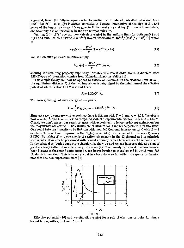
a normal,linearSchriJdingerequation in the mediumwithinducedpotentialcalculatedfromHNC. ForM _ 0, w22(k) is always attractive in k-space,irrespectiveof the sign of Sm andhenceof the impuritycharge.If one goes to finite densityn2 and Eq. (13) has a boundstate,one naturallyhas an instabilityin the two fermionmixture.
WritingQ_ = Z2e2 one can now calculatew_2(r)in the uniformlimit forboth Sl2(k) andS(k) and small M to be (with b = .),1/4)inversetransformof 4h_7_/[mk_(47 + k4)-1] whichis
g2e2=---(1 - e b,) (15)r
and the effectivepotential becomessimply
Z_e2Fell (r) = --e -br cos br, (16)r
showingthe screeningpropertyexplicitely. Notably this lowest orderresult is differentfromRKKY-typeof interactioncomingfrom Kohn-Luttingerinstability[12].
This simple theorycan nowbe appliedto varietyof instances. In the classicallimit M = 0,the equilibriumdistanceR ofthe two impuritiesis determinedby the minimumof the effectivepotential which is closeto bR - _rand hence
R = 1.26r,as4/t. (17)
The correspondingcohesiveenergyof the pair is
E = 1VeII(R ) ,_, -.246Z2r'_ 314 eV. (18)
Simplest case to compare with experiment here is lithium with Z = 3 and r, = 3.25. We obtainnowR = 3.1/t and E = -.9 eV as comparedwith the experimentalvalues3.4/_ and -1.6 eV.Clearly we don't expect ourresultto agreewith experiment in lowestorderapproximation butthe magnitudesarecorrect.The calculationforlithiumcouldinfact be performedin two ways:Onecouldtake the impurityto be He+-ionwith modifiedCoulombinteractionv¢(r) with Z = 1or else take Z = 3 and improveon the $12(k), since S(k) can be calculated accurately usingFHNC. By taking Z = 1 one avoidsthe exiton singularityin the 12-channeland in principlesuch a calculationcan beperformedwith desiredaccuracy,whichhoweveris not the point here.In the originalset both boundstate singularitiesshowup and wecan interpret this as a sign ofgood accuracyrather than a deficiencyof the set (9). The remedyis to treat the two fermionbound states as the secondcomponenti.e. usebosonfermionmixtureinsteadbut with modifiedCoulombinteraction. This is exactly what has been doneso far within the spectator fermionmodelof the new superconductors[4]
0.08 . .
0.06 _._0.04 )
0.00 I - "
-0.02
2 4 6 8 10
• ('.'o)FIG.2.
Effectivepotential (16) and wavefunction_b_2(r)for a pair of electronsor holes formingabound boson, with r, = 4 and M = .1.
312
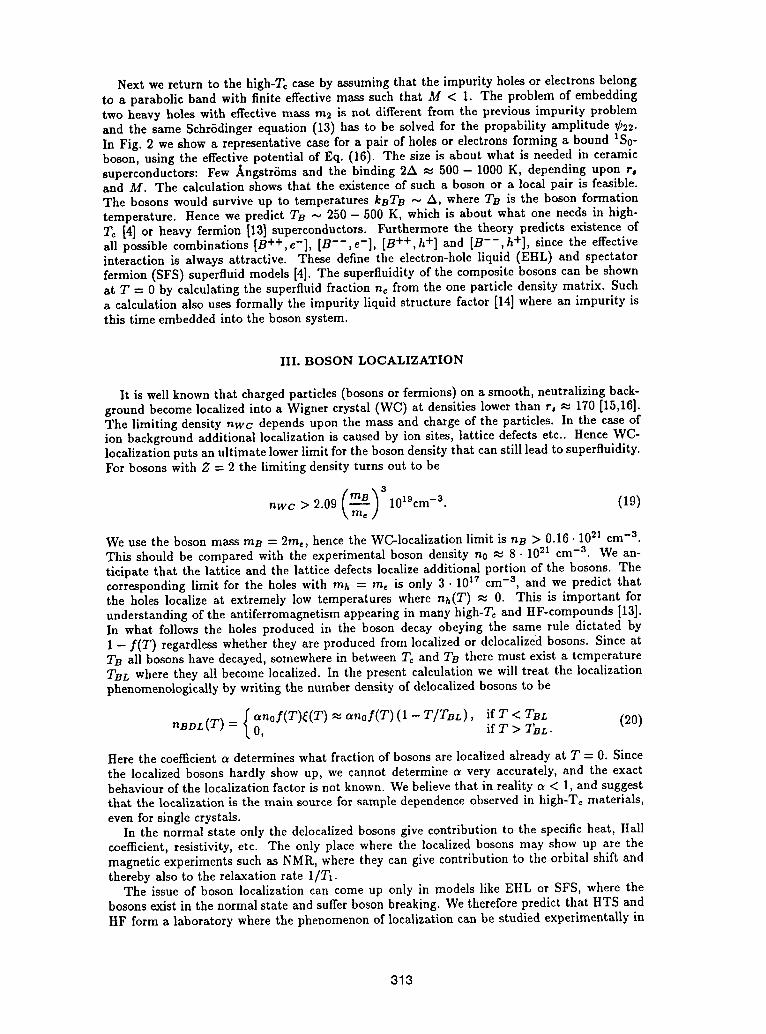
Next we return to the high-To case by assuming that the impurity holes or electrons belongto a parabolic band with finite effective mass such that M < 1. The problem of embeddingtwo heavy holes with effective mass m2 is not different from the previous impurity problemand the same Schrbdinger equation (13) has to be solved for the propability amplitude ¢22.In Fig. 2 we show a representative ease for a pair of holes or electrons forming a bound 1S0-boson, using the effective potential of Eq. (16). The size is about what is needed in ceramicsuperconductors: Few Angstrbms and the binding 2A _ 500- 1000 K, depending upon r,and M. The calculation shows that the existence of such a boson or a local pair is feasible.The bosons would survive up to temperatures kBTB "_ A, where TB is the boson formationtemperature. Hence we predict TB "_ 250 - 500 K, which is about what one needs in high-Tc [4] or heavy fermion [13] superconductors. Furthermore the theory predicts existence ofall possible combinations [B ++, e-l, [B--, e-l, [B ++, h+] and [B--, h+], since the effectiveinteraction is always attractive. These define the electron-hole liquid (EHL) and spectatorfermion (SFS) superfluid models [4]. The superfiuidity of the composite bosons can be shownat T = 0 by calculating the superfluid fraction nc from the one particle density matrix. Sucha calculation also uses formally the impurity liquid structure factor [14] where an impurity isthis time embedded into the boson system.
III. BOSON LOCALIZATION
It is well known that charged particles (bosons or fermions) on a smooth, neutralizing back-ground become localized into a Wigner crystal (WC) at densities lower than r, _ 170 [15,16].The limiting density nwc depends upon the mass and charge of the particles. In the case ofion background additional localization is caused by ion sites, lattice defects etc.. Hence WC-localization puts an ultimate lower limit for the boson density that can still lead to superfluidity.For bosons with Z -- 2 the limiting density turns out to be
>509(m 3101°cm-3. (19)\me /
We use the boson mass mB= 2m_, hence the WC-localization limit is nB> 0.16.1021 cm -3.This should be compared with the experimental boson density no _ 8 • 1021 cm -3. We an-ticipate that the lattice and the lattice defects localize additional portion of the bosons. Thecorresponding limit for the holes with mh = me is only 3 • 1017 cm -3, and we predict thatthe holes localize at extremely low temperatures where nh(T) _ O. This is important forunderstanding of the antiferromagnetism appearing in many high-To and HF-compounds [13].In what follows the holes produced in the boson decay obeying the same rule dictated by
1 - f(T) regardless whether they are produced from localized or delocalized bosons. Since atTB all bosons have decayed, somewhere in between Tc and TB there must exist a temperatureTBL where they all become localized. In the present calculation we will treat the localizationphenomenologically by writing the number density of delocalized bosons to be
(anof(T)_(T) ._ anof(T) (1 - T/TBL), if T < TBL (20)nBDL (T) = O, if T > TBL.
Here the coefficient a determines what fraction of bosons are localized already at T = O. Sincethe localized bosons hardly show up, we cannot determine a very accurately, and the exactbehaviour of the localization factor is not known. We believe that in reality cr < 1, and suggestthat the localization is the main source for sample dependence observed in high-T€ materials,even for single crystals.
In the normal state only the delocalized bosons give contribution to the specific heat, Hallcoefficient, resistivity, etc. The only place where the localized bosons may show up are themagnetic experiments such as NMR, where they can give contribution to the orbital shift andthereby also to the relaxation rate 1/7'1.
The issue of boson localization can come up only in models like EHL or SFS, where thebosons exist in the normal state and suffer boson breaking. We therefore predict that HTS andHF form a laboratory where the phenomenon of localization can be studied experimentally in
313
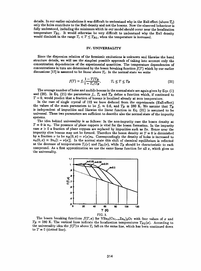
details. In our earliercalculations it was difficult to understandwhy in the Hall effect (above To)only the holes contribute to the Hall-densityand not the bosons. Now the observed behaviourisfully understood, includingthe minimum which in ourmodel should occur near the localizationtemperature TBL. It would otherwise be very difficult to understand why the Hall densitywould diminish in the range Tc < T _<TBL, when the temperature is increased.
IV. UNIVERSALITY
Sincethe dispersionrelationof the fermionicexcitationsis unknownand likewisethe bandstructure details, we will use the simplest possibleapproachof taking into account only theconcentrationdependenciesof the experimentalquantities. The temperaturedependenciesofconcentrationsin turn aredeterminedby the bosonbreakingfunction .f(T) whichby ourearlierdiscussions[17]is assumedto be linearaboveTo. In the normalstate wewrite
1- T/TBf(T) = fc i -- Tc--_B' T¢ < T < TB (21)
The average number of holes and mobile hosons in the normal state are again given by Eqs. (1)and (20). In Eq. (21) the parameters fc, Tc and TB define a function which, if continued toT = 0, would predict that a fraction of bosons is localized already at zero temperature.
In the case of single crystal of 123 we have deduced from the experiments (Hall-effect)the values of the main parameters to be fc _ 0.6, and TB = 280 K. We assume that TBis independent of impurities and likewise the linear function in Eq. (21) is assumed to beuniversal. These two parameters are sufficient to describe also the normal state of the impuritysystems.
The idea behind universality is as follows: In the non-impurity case the boson density atT = 0 is no. The presence of plane coppers is vital for the boson formation. In the impuritycase z > 0 a fraction of plane coppers are replaced by impurities such as Zn. Hence near theimpurity sites bosons may not be formed. Therefore the boson density at T = 0 is diminishedby a fraction v to be nB(0, x) - v(x)no. Correspondingly the density of holes is increased tonh(0, x) = 2n011 -- v(x)]. In the normal state this shift of chemical equilibrium is reflectedas the decrease of temperatures To(v) and TBL(V), while TB should be characteristic to each
compound• As a first approximation we use the same linear function for all z, which gives usthe universality.
1.1
.0.g
•S '
.4 •
.,10 20 4o 60 Io 100 120
FIG. 3.The boson breakingfunctions f(T,z) for YBa_(Cul-xZnx)30_ with four values of z and
TB = 280 K. The verticallines indicate the localization temperaturesTBL(Z). Accordingtothe universalityidea the f(T):s aboveTcfall on the same line, whichhas been continueddownto T = 0 (dotted line).
314
The idea of universallinear.f(T) aboveTc is illustratedin Fig. 3. In fact wehave gone onestep furtherby assumingthat the universalityis truealsofordifferentoxygencontents6, whichcontrols the densityno in YBazCuaO¢__. In Fig. 4 we comparethe Hall density calculatedusing a universalf(T) with the one reportedby Jones et aL [18].Theresult supports the ideaof universalf(T) aboveTo: In the range0 < 8 < 0.5 the data is quite wellreproducedwith no
the only freeparameter.
2.0
1.5.f"
1.0
0.5
0.00 100 200 300
Temperature(K)FIG. 4.
The Hall densitywith severaloxygencontents in YBCO thin films. The short thick curvesrepresentthe experimentaldata of Ref. [18]. The theoreticallines were calculatedusing therelation(eRH)-1 = 2n011-- .f(T)] with the same linearf(T) for all oxygencontents.The onlychangingparameter is no. The f(T) is given by Eq. (21) with the fixedparametersT_ = 92 K,TB = 300 K, and f_ = 0.6. This resultdemonstratesthat .f(T) aboveTc is fairly independentof the oxygen content.
The universality allows us to calculate To, the localization temperature TB£, and fc as afunction of impurity content z from Eqs.
vf(TBL(V))""f(TBL(1))
vf(Tc(,)) = f(Tc(1)) , (22)
where v is related to the impurity concentration z by 1 - v _ 7x (determined from the NMRexperiment of Ref. [2]). Eqs. (22) are based on the fact that localization or the supetfluidtransitions take place at a fixed boson density for the same crystalline background. UsingEqs. (21) and (22) one obtains the following formula for the T_ depression:
T¢0/) = _,-l[Tc(1) - (1 - _')TB], (23)
or
T_(=)= T_(0)- 5=TB1- 5= ' (24)
where TB ,_ 300 K and factor 5 comes from the valence counting for 123 discussed by Harashinaet al. [20]: The Zn impurity atoms replace only coppers in the ab plane, and _7 _ 5. This givesquantitative agreement with experiment [20]. The pole appearing in Eq. (24) for unphysicalnegative values of To(=) causes down bending of the curve which is observable in the case ofLa_-ySryCul-xZnxO4 in the data of the same group. Also the T_ depression of Pr and Cesubstituted Bi2122 seems to bend down in a similar fashion [21]. Harashina et al. give anextensive discussion of the "spin gap", which they conclude to be connected with localization ofholes. Here we associate the minimum in the Hall coefficient Rab with boson localization, whichexplains in a simple way the existence of the minimum in Rab near TBL _ 100 K in 123 [20].From the universality idea we obtain for the localization temperature TBL(V) the relation
TBL(v) -- To(z,) = z/-1 [TBL(1) -- To(l)]. (25)
315
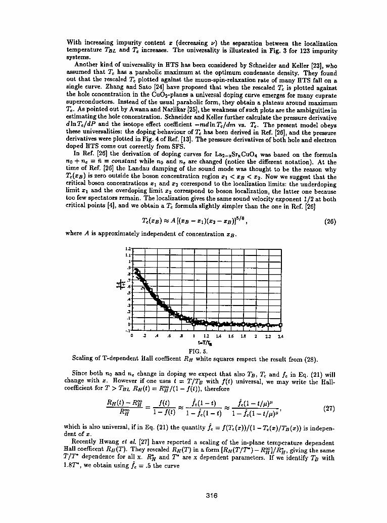
With increasing impurity content z (decreasing v) the separation between the localizationtemperature TB/: and Tc increases. The universality is illustrated in Fig. 3 for 123 impuritysystems.
Another kind of universality in HTS has been considered by Schneider and Keller [23], whoassumed that Tc has a parabolic maximum at the optimum condensate density. They foundout that the rescaled Tc plotted against the muon-spin-relaxation rate of many HTS fall on asingle curve. Zhang and Sato [24] have proposed that when the rescaled Tc is plotted againstthe hole concentration in the CuO2-planesa universal doping curve emerges for many cupratesuperconductors. Instead of the usual parabolic form, they obtain a plateau around maximumTo. As pointed out by Awana and Narlikar[25],the weaknessof such plots are the ambiguities inestimating the hole concentration. Schneiderand Keller furthercalculate the pressurederivativedlnT¢/dP and the isotope effect coefficient -mdlnT¢/dm vs. To. The present model obeysthese universalities: the doping behaviour of Tc has been derived in Ref. [26], and the pressurederivatives were plotted in Fig. 4 of Ref. [13]. The pressurederivatives of both hole and electrondoped HTS come out correctly from SFS.
In Ref. [26] the derivation of doping curves for La2-xSrxCuO4 was based on the formulano -t-ne = fi -- constant while no and ne are changed (notice the different notation). At thetime of Ref. [26] the Landau damping of the sound mode was thought to be the reason whyTc(zB) is zero outside the boson concentrationregion zl < zB < z2. Now we suggest that thecritical boson concentrationsxl and z2 correspond to the localization limits: the underdopinglimit zl and the overdoping limit z2 correspond to boson localization, the latter one becausetoo few spectators remain. The localization gives the same sound velocity exponent 1/2 at bothcritical points [4], and we obtain a Tc formula slightly simpler than the one in Ref. [26]
T(xB) A[(xB- xl)(x2- =B)]5/8, (28)where A is approximately independent of concentration zB.
1.1
I
.9
" lla
4 "h:ta "_k
°..| i , t
0 .2 .4 .6 .8 1 1.2 1.4 1.6 1.8 2 2.2 2.4
t-T/rBFIG.5.
Scaling of T-dependent Hall coefficent RH white squares respect the result from (28).
Since both no and ne change in doping we expect that also TB, T¢ and fc in Eq. (21) willchange with z. However if one uses t - T/TB with f(t) universal, we may write the Hall-coefficientforT > TB, RH(t)= R/(1 -/(t)), therefore
RH(t) -- R°_ _ f(t) /¢(1 - t) re(1--tip)"R_ 1 - f(t) 1 - re(1 - t) 1 - f¢(1 - t/p)"'
which is also universal, if in Eq. (21) the quantity L = f(T,(z))/(1 -T,(z)/Tn(z)) is indepen-dent of z.
Recently Hwang el aL [27] have reported a scaling of the in-plane temperature dependentHall coefficent RH(7").They rescaled Rtt(T) in a form [a.(T/T')- giving the sameT/T* dependence for all x. R_t and T ° are x dependent parameters. If we identify TB with1.8T*, we obtain using f_ = .5 the curve
316
1--t
- = T U' (28)which is shown in Fig. 5 to be in rather good agreement with experiment. The last, non-linearform in Eq (27) with critical exponent # > 1 would give good agreement without rescaling of t.
V. CONCLUSIONS
Weconcludethat simplemicroscopictheorypredictsthepossibilityof bosonformationin thesituation wherethe backgroundelectronor hole liquid(the spectators) have smallereffectivemass than the pairing fermionswhichbelow temperatureTs combinepairwiseinto bosons.Sincethe approximatecloseformeffectivepotentialV_II(r) by Eq. (16)givesa reasonablevaluefor the unit cell of Li-metal and also the cohesiveenergywe believethat it is fairly accuratealsoin the quantummechanicalbosonproblemforone to add theeffectsof unisotropiespresentin ceramicsuperconductors.The knowledgeof boson wavefunction enables one to calculatethe densityof states and hence f(T) from the boson decay at finite temperatureby simplycalculatingthe scatteringstates fromEq. (13) with E > 0.
The present theoryof bosonbindingis differentfrom BCS phonon couplingand also fromthe bipolaronmodel.
[1]N. P. Ong, in: PhysicalPropertiesof High-TemperatureSuperconductorsII, ed. D. M.Ginsberg(WorldScientific,Singapore,1990)p. 459.
[2]K. Ishida, Y. Kitaoka,T. Yoshitomi,N. Ogata, T. Kaminoand K. Asayama, Physiea C179(1991)29.
[3] C. Thomsen and M. Cardona, in: Physical Properties of High-Temperature Superconduc-tors I, ed. D. M. Ginsberg (World Scientific, Singapore, 1989) p. 409.
[4] A. Kallio, V. Apaja, X. Xiong and S. PSykkS, Physica C 219 (1994) 340-362.[5] A. Kallio and R. A. Smith, Phys. Left. 68B (1977) 315; R. Abe, Progr. Theor. Phys. 19
(1958)407.[6] D. Ceperley, Phys. Rev. B 18 (1978) 3126.[7] S. Fantoni and S. Rosati, Nuovo Cim. 25 (1975) 593; Nuovo Cim. Left. 16 (1976) 531.[8] J. G. Zabolitzky, Phys. Rev. B 22 (1980) 2353.[9] P. Pietiliiinen and A. Kallio, Phys. Rev. B 27 (1983) 224.
[10] T. Chakraborty, A. Kallio, L.J. Lantto and P. Pietiliiinen, Phys. Rev. B27 (1983) 3061.[II] J. C. Owen, Phys. Rev. Left. 47 (1981) 311.[12] W. Kohn and J.H. Luttinger, Phys. Rev. Left. 15 (1965) 524.[13] A. Kallio and X. Xiong, Physica C 199 (1992) 340; A. Kallio, S. PSykk5 and V. Apaja,
submitted to Physica C.[14] M. Puoskari and A. Kallio, Phys. Rev. B 30 (1984) 152.[15] E. P. Wigner, Phys. Rev. 46 (1934) 1002.[16] K. Moulopoulos, and N. W. Ashcroft, Phys. Rev. Lett. 69 (1992) 2555.[17] A. Kallio, V. Apaja, and X. Xiong, Physica C191 (1992) 23.[18] E. C. Jones, D. K. Christen, J. R. Thompson, R. Feenstra, S. Zhu, D. H. Lowndes,
J. M. Phillips, M. P. Siegal and J. D. Budai, Phys. Rev. B47 (1993) 8986.[19] T. R. Chien, D. A. Brawner, Z. Z. Wang, and N. P. Ong, Phys. Rev. B43 (1991) 6242;
N. P. Ong, in Physical Properties of High Temperature Superconductors II, Ed. D. M. Gins-berg (World Scientific, Singapore, 1990) p. 459.
[20] H. Harashina, T. Nishikawa, T. Kiyokura, S. Shamoto, M. Sato, and K. Kakurai, PhysieaC212 (1993) 142.
[21] V. P. S. Awana, S. K. Agarwal, A. V. Narlikar, and M. P. Das, Phys. Rev. B48 (1993)1211.
[22] V. Apaja, and A. Kallio, Physica C 209 (1993) 519.[23] T. Schneider, and H. Keller, Phys. Rev. Lett. 69 (1992) 3374.[24] H. Zhang, and H. Sato, Phys. Rev. Left. 70 (1993) 1697.[25] V. P. S. Awana, and A. V. Narlikar, Phys. Rev. Left. 71 (1993) 303.[26] A. KaIIio, X. Xiong, Phys. Rev. B43 (1991) 5564.[27] H.Y. Hwang, B. Batlogg, H. Takagi, H.L. Kao, J. Kwo, R.J. Cawa, J.J. Krajewski and
W.F. Peck Jr., Phys. Rev. Left. 72 (1994) 2636.
317
THERMOMAGNETIC PHENOMENA IN THE MIXED STATE
OF HIGH TEMPERATURE SUPERCONDUCTORS
E.Z.Meilikhov, RSC '°Kurchatov Institute", 123182 Moscow, Russia
i. Introduction
Galvano- and thermomagnetic phenomena in conductors areusually described with the help of kinetic coefficients which aredetermined with the following expressions for electric field Eand the electron fraction of the heat flow q [I]:
E=PxxJ+Pxy[k×j]+_VT+QB[k×VT ], (1)
q =nj+E_B[ kxj]-_VT+LB[kxVT ]. (2)
Here P×x and Pxy are components of the resistivity tensor; j is acurrent density; k=B/B is a unit vector parallel to magneticfield B; _, Q, H, E, _, and L are Seebeck, Nernst, Peltier,Ettingshausen, heat conductivity and Righi-Leduc coefficients,respectively. In accordance with the Onsager principle, some ofthese coefficients are interconnected:
H:aT, E_:QT. (3)
On the other hand, there is also a connection between theelectric field and the heat flow in the superconductor mixedstate. If one assumes that both the electric field and the heatflow arise only under the fluxoid motion then we have Josephsonformula for the electric field:
E=-_[ vfxB ] (4)
and Huebener relationship for the heat flow [2]:
q=S_Tnfvf , (5)
where vf, nf=B/¢0 are an average motion velocity and a fluxoids
density _@0=hc/2e is a magnetic flux quantum), and S_ is anentropy of a unit section of a fluxoid. It follows from Eqs.(4)and (5):
q=T (cS4/¢0)[Exk]. (6)
318
For given values of the magnetic field and temperature thevelocity of the fluxoid motion vf depends only on the current
density j and the temperature gradient VT. For a general case the
dependence of vf on j and VT has the form:
vf=alJ + a2[jxk ] . a3VT + a4[VT×k ] (7)
(a specific form of coefficients al, a2, a3, and a4 depends onthe choice of the fluxoid motion model, see below). SubstitutingEq.(7) into (4) and (5), we obtain
E=(a2B/c) j + (alB/C)[kxj] + a4BVT - a3B[kxVT], (8)
q=(nfTS4al) j - (nfTS4a2)[kxj] + a3VT- a4[k×VT ]. (9)
The comparison of these relations with general expressions (i)and (2) for E and q and the use of the Onsager equation (3) leadus to
s s
as=(CS_/¢0)P×y , QsB=-(cS_/¢0)P×x , (I0)
where index s marks kinetic coefficients relating to asuperconductor in the mixed state. Eqs.(10) which are aconsequence of the connection (6) between q and E in the mixedstate of a superconductor forecast a certain correlation between
s s
"heat" and "current" coefficients (es' Qs and Px×' Pxy) and givea possibility of checking the correctness of the conceptioninvolved.
The most detailed experimental researches of kineticcoefficients in the superconductor mixed state have been carriedout for high temperature superconductors [3,4] where their valueis essentially higher and the temperature range accessible formeasurements is noticeably wider than those for traditionalsuperconductors. The researches revealed the real connectionsbetween kinetic coefficients to be strongly different from thosepredicted by relations (i0). Thus, for instance, Hall resistance
Pxy in the mixed state is often a nonmonotonic and evensign-reversing function of temperature and magnetic field.Meanwhile Seebeck coefficient (thermal power) usually risesmonotonically with the T or B increase and its behavior, as arule, resembles that of the longitudinal resistance'e a Pxx"
Besides, according to Eq.(10), the Seebeck coefficient goes to azero on the normal state transition (since in this case entropy
S_ goes to a zero), although this coefficient obviously shouldtake the value peculiar for the normal state. All this testifiesto the fact that Eq.(10) is based on incorrect premises. It isclear that these are only Eqs. (4) and (5) (ensuing from anassumption that the electric field generation and the heat
319
transfer and, consequently, all the kinetic phenomena in thesuperconductor mixed state are related solely to the fluxoidmotion) may be erroneous.
This approach is applicable in full measure only far from thesuperconducting transition, where fraction N =n /N of normaln n
quasiparticles is small (N and nn are normal quasiparticles
concentrations at T>Tc and T<Tc, accordingly). In conformity with
the weak coupling BCS theory such particles originate only due totheir excitation via energy gap _, and hence in low temperaturesuperconductors (with a weak electron-phonon interaction) normalquasiparticles appear in a noticeable quantity only in a directproximity to T when the width of superconducting gap _ becomesc
close to (or smaller than) thermal energy kT. Thus, this approachis valid almost everywhere but for a narrow temperature rangenear the transition.
A different situation occurs in high-temperature super-conductors with a marked tendency towards a strongelectron-phonon interaction resulting in the finite density ofstates within the energy gap [5]. In this case normalquasiparticles arise mainly owing to filling these states andtheir concentration is determined by a power-law dependence
(e.g , by law Nn_(T/Tc)4• , known for a Gorter-Casimir two- liquid
model [6]) rather than by temperature exponential dependenceN (T) a exp(-A/kT). The temperature range where fraction ofN w
normal quasiparticles is large, grows much broader and there isno groun_ to neglect their contribution into different kineticphenomena In Ref.[5] numerous references are made to the workswhich point out that the temperature dependences of thermalproperties of high temperature superconductors near T are much
c
better described by the Gorter-Casimir phenomenological modelthan by weak coupling BCS theory. In this connection thedescription of kinetic properties of the mixed state of hightemperature superconductors requires a simultaneous andself-consisted account for the motion of fluxoids and normalquasiparticles.
The most straightforward way here is to proceed from anassumption that corresponding contributions into kineticcoefficients are independent and additive. And it exactly thisway which is usually taken (see, e.g., Refs.[7 and 8]). Thisapproach presupposes, in particular, that the presence of normalquasiparticles effects in no way the fluxoid motion (and,consequently, the electric field in a superconductor). This key
1Here by the term "normal quasiparticles" we understand not the
particles which are "bound" in the fluxoid cores (with theconcentration of N) but those which are outside the fluxoid coresand are "free" (their concentration is n <N).
n
320
assumption is corroborated with no due arguments and is simplypostulated although it does not look absolutely obvious• So oneneeds to get rid of this limitation and to construct aself-consisted theory of galvano- and thermomagnetic phenomena inthe superconductor mixed state within a frame work of a singlemodel. Since at present the fluxoid motion is describedapproximately even in neglect for normal quasiparticles [9] aphenomenological approach analogous to that used in the classicalwork by Gorter-Casimir [6] might be used.
2. Seebeck and Nernst Effects
Average density Jn of the normal quasiparticle current is
determined by the standard relationship:
N E+aN [Exk]__NIVT__N2[VTxk ] (Ii)Jn=Oxx xy
N and oNwhich takes into account that conductivity (axx xY) of a
system of normal quasiparticles (metal) is proportional to theirconcentration Nn while Seebeck (aN) and Nernst (QN) coefficients
• N Nare independent on it2 Here _N]=aNaxx+QNBaxy and
N N
_N2=_Naxy-Q_Baxx. The electric field in a conductor with finiteconductance is determined by well-known relations, namely, theOhm's law
N . N
E=Pxx]n+Pxy[kxJn]+aNVT+QNB[kxVT ] (12)
for a normal metal and Josephson's formula (4) for asuperconductor in the mixed state without normal quasiparticles.
N Nare components of resistivity tensor of a normalHere Pxx and Pxy
metal. How could one generalize Eqs.(4), (12) corresponding totwo limiting situations (N =0 and N =I) for a common case whenn n
0<N <i? In the absence of an exact answer to this question onen
may try the interpolation formula
S:-f {_[ vfxS ]}+fn{p: " N }3n+Pxy[kxj ]+eNVT+QNB[kxVT ] (13)s x n
where weight factors fs and fn have to satisfy conditions
2In normal metal _, Q _ kT/EF [i] where Fermi energy aF is determ
the total concentration of charge carriers and is independent on Nn.
321
fs(Nn=0) =i, fs(Nn=0)=0, f (Nn=l) =I which ensure the transfer ofn
Eq.(13) into "correct" expressions (4) and (12) in the abovecited limiting cases. The expression for an electric field whichis obtained after substitution of Eq.(ll) into (13) contains noterms proportional to VT (it is required for obvious equality E=0to take place at vf=0) and has the form
f
E s
As it can be seen from Eq.(14), in order to determine an electricfield it is necessary to find the velocity of fluxoid motion vf
for which purpose let us use the equation of motion suggested inRef [I0] (when N =0, VT=0) :• n
_m[VsXk] - Dm[Vfxk] - _±vs - _,vf = 0, (15)
where um=nse_0/c, ns is a concentration of superconducting
carriers; vs is their (average) current velocity; and _i and _llare viscosity coefficients. The existence of normal current Jn
(for N /0) should have brought about the appearance of an
v -dependent function A(vn) in Eq (17) Since at N _ 1 all the• " nn
terms occurring in Eq.(17) go to a zero, the equation of fluxoidmotion in this case come to relation A(Vn)=0 coinciding with the
equation of normal quasiparticles motion, i.e., to the Ohm's law<I variables v and v in the mo-
(12). We may assume that at Nn s n
tion equation are also "divided", in other words, the equation is"split" into two expressions: A(Vn)=0 (coincides with Eq.(ll) )
and Eq.(15).Now let us discuss the way of modification of the fluxoid
motion equation (15) with the presence of the temperaturegradient. Firstly, "thermodynamic" force FT! = -S_VT must
manifest itself in it. Here S_=S_(T) is a temperature dependent
entropy of a fluxoid section of a unit length. This force is ananalogy [2] for Lorenz force _m[Vs×k] and can be derive from the
latter by substituting Vs4 v*=(S_/_m)[VTxk]. Simultaneously force
FT2 .analogous to "viscosity" force -U±v s from Eq.(15) should beintroduced; it is derived from the latter by means of the same
v*: = -S_(_/_m) [VTxk]-substitution vs FT2Another reason for appearance of "thermal" forces in the
fluxoid motion equation is the origination of counterflowsupercurrent in-between their normal cores Ill]. If there is atemperature gradient inside the fluxoid core (that is in the
322
region where Nn=l) there appears additional normal current with
the density, according to Eq. (ii), equal to JT = -_NIVT-
-_N2[VTxk]. This current is balanced with externally flowing
counterf low current with an average density jb=Jbs+Jbn= -JT'
which is a sum of supercurrent Jbs and normal current Jbn" The
superconducting component of this current equals Jbs = NsJb =V it is a
-NsJT. Similarly to the transport supercurrent Js=ens ssource of forces effecting fluxoids [12]. Hence two more forces
FT3=- (_m/Ne)(_NI[VTxk]-_N2VT) '(16)
FT4=(n±/Ne) (_NIVT+_N2[VTxk]
should be introduced into fluxoid motion equation (15) related tothe case when VT=0. These forces are derived from Lorenz force
_m[VsXk] and viscous force -_±vs by means of substitution v3 s
-v**, where v**= Jbs/ens = - (I/eN)JT
Thus, in the presence of VT the fluxoid motion equationacquires the form:
_m [VsXk]- __Vs - [S_ [_] + [_] (_Tm/_NI-_7_L_N2)] [VTxk] -
Using expression Js=ensVs=j-jn (where the normal current follows
Eq. (Ii) ) and substituting relationship Vs=C[ExB][ (l-Nnfn)/fsI/B2
ensuing from Eq.(14) into Eq.(17) we obtain the equation for theelectric field. The solution of that equation in respect to Egives the relationship determining the transport coefficients ofsuperconductors in the mixed state : a Seebeck coefficient(thermal power)
3The negative sign appeared in the v _ -v** substitution is as
result of the reverse (in respect to the normal current )direction of supercurrent Jbs" The nondiscrepancy of the fluxoidmotion equation (17) thus obtained is confirmed by thefulfillment of the Onsager relationship for calculated kineticcoefficients (see below).
323
N N +Q.B( a - o ) + (cS_/_0)pxy (18)a=N n aN(Pxx°xx+Pxy°xy ) Pxx xy Pxy xx
and Nernst coefficient
N _ (aN/B) (PxxoN_ _ ]Q=Nn °xx+Pxy°xy)- xy Pxy°xx) -(cS_/B_0)Pxx" (19)
It is easy to see that for normal metal (Nn=I, S_ =0) Eqs. (18)
and (19) give _=aN and Q=QN' and in the superconducting state (no
fluxoid motion, P<Pc and Pxx = Pxy = 0), as it might be expected,
a=Q=0. Thus, Eqs. (18) and (19) are true for a whole transitionregion of the resistive mixed state of a superconductor.
3. Heat conductivity.
Peltier, Ettingshausen and Righi-Leduc Effects
Heat flow qs' related to the entropy transfer with moving
fluxoids, equals qs=S_TnefVf, where nef is effective density ofmoving fluxoids which is different from their real density
nf=B/_0. Nevertheless, rewriting Eq. (14) in the form E=-(1/c) [vf
x B](nef/nf) we come to the relation
qs=T (cS_/_0)[E×k],
which is an analogy to Eq.(6). As to the heat flow due to thenormal quasiparticle motion, it is defined by the relationship
qn=nNJn+EN_NB[kxj,]+Nn [-_N_T+LNB[kxVT ]], (20)
which accounts for _N and LN being proportional to current
carrier concentration Nn while HN and the product EN_N are
independent on it.Thus, the electron component of the heat flow in a
superconductor equals
.cs .q:qs+qn:T [ ¢0][E×k ]+HNJn+E_B[ kxjn]+Nn[-_NVT+LNB[kxVT ]]. (21)
To deduce corresponding kinetic coefficients is possible by meansof expressing q in terms of total transport current j. First letus find the connection between normal and total currentssubstituting Eq.(1) into Eq.(ll) :
[Jn=Nn J(Pxx°_x+Pxy°_y)+[kxj](Pxy°xx-Pxxax
324
-(_NI-Nn_I)vT - (_N2-Nn_2)[VTxk] (22)
where _I=(°N _+°_yQB)xx , _2=(o_ya-O_xQB) . Next, substitutingEqs.(1) and (22) into (21) we come to expression (2) wherePeltier coefficient
[ N N N N ]_=N _N (Pxxon xx+Pxyaxy)+EN_NB(Pxx°xy-Pxy°xx) + T(cS_/_0) Pxy (23)
Ettingshausen coefficient
(E_B)=Nn N_NB(PxxOxx+PxyOxy)-gN(OxxOxy-PxyOxx ) -T(cS¢/¢0)Pxx, (24)
heat conductivity coefficient
_=Nn_N+nN (_NI-Nn_I)+EN_NB(_N2-Nn_2)-T(cS_/@o) QB, (25)
and Righi-Leduc coefficient
LB=NnLNB+HN (_N2-Nn_2)-EN_NB (_NI-Nn_])-T (cS_/¢0)a. (26)
Proceeding from the Onsager equation for a normal metal
(HN=aNT, EN_N=QNT) we make sure that Onsager equations (3) arealso valid for above given Seebeck and Peltier coefficients(compare Eqs.(18) and (23)) as well as for Nernst andEttingshausen coefficients (compare Eqs.(19) and (24)) for asuperconductor in the mixed state. This is an evidence ofinherent nondiscrepancy of the model suggested and, inparticular, of a correct form of the fluxoid motion equation(17). The latter might be obtained without defining concretelyexpressions for "thermal" forces FTI-FT4. It would be sufficientfirst to obtain relations (18) and (19) for a and Q, proceedingfrom Onsager relations and Eqs. (23) and (24) for H and Ecoefficients, and then to "restore" the fluxoid motion equation(17).
The Hall conductivity (resistance) is known to besufficiently lower than the longitudinal conductivity(resistance) at any temperature [3,4]. It gives a possibility tosimplify noticeably the expression obtained for kineticcoefficients:
a=HIT _ NnaN(pxx/pn)+(cS_/¢O)Pxy _ Nn(_N(Pxx/PN), (27)
Q:(E/gT) _ NnQN(Pxx/PN)-(cS_/B_o)Pxx :_- (cS#/B¢0)Pxx, (28)
325
_ Nn_N , (29)
LB_NnLNB-T(cS_/¢O)_-NnaNT(CS_/_O)(Pxx/PN). (30)
The first two of them were derived in earlier works in a notquite correct way [i, 2, ii, 13].
Let us emphasize that the expressions derived forcoefficients a, Q, H, E, _ and L are universal, i.e., independenton the choice of coefficients f and f . The latter determine
s n
only the connection between total conductivity of asuperconductor in the mixed state and "partial conductivities",related to normal quasiparticles and fluxoids [14].
From the expressions obtained for kinetic coefficients e, Q,H, E, _, and L of a superconductor in the mixed state it is seenthat each of them consists of two terms, one of which isproportional to concentration N of normal quasiparticles and then
other is to the S_ entropy of fluxoids. These two parts may be4
conditionally called "normal" and "fluxoid" contributions Theirrole in different kinetic coefficients is not identical.Longitudinal effects (described with coefficients e, H, and _)are defined basically with the "normal" contribution, whiletransverse effects (coefficients Q, E, and L) are governed by the"fluxoid" one. It is due to the following:
I) Seebeck and Peltier coefficients e, and H : a relatively
minute value of the fluxoid entropy (cS_PN/aN_ 0 _ R << Pxx/Pxy)
and a absolutely small Hall angle (p×x/Pxy >> i); the vortices arealmost immovable along the temperature gradient and transfersmall (in comparison with normal electrons) energy;
2) Nernst and Ettingshausen coefficient: a relatively large
value of the fluxoid entropy (cS_PN/_N_0 _ R >> I) and a
relatively small Nernst coefficient QN in the normal state
(QNB/eN _ 7b << i); fluxoid transfer high (as compared to normal
electrons) energy in the direction perpendicular to thetemperature gradient;
3) Heat conductance and Righi-Leduc coefficients _ and L: allthe above-said conditions and a relatively high electron heat
conductance in the normal state (_NPN/Tc_N >>i) ; the vortices are
4The conventionality of this division can be seen if only fromthe fact that the "normal" contribution into kinetic coefficients
is related to the longitudinal resistivity Pxx' which, at least
to a certain extent, is determined by the fluxoid motion.
326
almost immovable along the temperature gradient ant transfersmall (in comparison with normal electrons) energy.
A good agreement with experimental data for HTSC of differentcompositions has been achieved for a different selection of
=N_ f =Nu [14]. The valuesinterpolation factors of the form fs s' n n
= u =I for YBa2Cu307_6 and _ = u =3/2 for Bi-2223 were shown to
provide the best fit.. A possible reason for these differentvalues is the different degree of anisotropy of the two compoundsin question. This problem, however, is to be further analyzed.
REFERENCES
I. A.A.Abrikosov, Fundamentals of the Theory of Metals, Elsevier,New York, 19882. Huebner R.P., Magnetic Flux Structures in Superconductors,Springer Verlag, Berlin, 19793. Dascoulidou A. et al., Physica C, 1992, v.201, p.2024. Freimuth A., Transport Properties in the Mixed State of HighTemperature Superconductors, Preprint, 19925. V.L.Ginsburg, E.G.Maksimov, SPCT, 1992, vol.5, p.1543 (inRussian)6. C.J.Gorter, H.B.G.Casimir, Zs.Phys., 1934 voi.35, p.963;Zs.Techn. Phys., 1934 vol.15, p.5397. Z.D.Wang, C.S.Ting, Phys.Rev. Lett., 1992 voi.69, p.14358. H.-C.Ri et al., Phys.Rev. B, 1991, v.43, p.137399. Z.D.Wang, C.S.Ting, Phys.Rev. B., 1992 voi.46, p.28410.S.J.Hagen et al., Phys.Rev. B, 1990 vol.41, p.I1630ll.A.V.Samoilov, A.A.Yurgens, N.V.Zavaritskii, Phys.Rev., 1992,v.46, p.664312.R.Huebener et al., Thermoelectric and Thermomagnetic Effectsin High Temperature Superconductors, Preprint, 199213.R.P.Huebener, Physica C, 1990, v.168, p.60514.Meilikhov E.Z. and Farzetdinova R.M., 1994, Physica C, v.221,p.27
327
SPECTROSCOPY OF INFRARED-ACTIVE PHONONSIN HIGH-TEMPERATURE SUPERCONDUCTORS
A.P. Litvinchuk
Department of Physics, Chalmers University of Technology,S-41296 GSteborg, Sweden
C. Thomsen
Institut fiir FestkSrperphysik, Technische Universith't Berlin,Hardenbergstrafle 36, D-10623 Berlin, Federal Republic of Germany
M. Cardona
Max-Planck-Institut fiir FestkSrperforschung,Heisenbergstrafle 1, D-70569 Stuttgart, Federal Republic of Germany
L. B6rjesson
Department of Physics, The Royal Institute of Technology,S-10044 Stockholm, Sweden
For a large variety of superconducting materials both experimental and theo-retical lattice dynamical studies have been performed to date. The assignment ofthe observed infrared- and Raman-active phonon modes to the particular latticeeigenmodes is generally accepted (for a reviews see Ref. [1-5]). We will concen-trate here upon the analysis of the changes of the infrared-phonon parameters(frequency and linewidth) upon entering the superconducting state which, as willbe shown, may provide information on the magnitude of the superconductivity-related gap and its dependence on the superconducting transition temperatureTc.
Effects of the superconductivity-induced infrared-phonon renormalizationwere studied experimentally most intensively for Y2Ba4Cu6+nO14+,_s(n = 0,1, and 2) superconductors with a double CuO2-1ayerin each primitive cell. Aninteresting feature of the materials with single-CuO chains as structural element(n -- 0 and 1) is the possibility to gradually modify their superconducting pro-perties by varying the oxygen content; this allows to study the effectsof a reducedTc in detail even for materials of the same crystallographic structure. For n = 2,however, the presence of the double-CuO chains fixes the oxygen content and, cor-respondingly, To. Another possible way to investigate the effects of phonon renor-malization and their connection to superconductivity is to study ion-substitutedsuperconductors knowing the effectsof the ions on the superconducting propertiesof materials from independent measurements.
Superconductivity-induced phonon self-energy effects or so called phononanomalies were found rather soon after discoveryof YBCO superconductors [6, 7].For a number of reasons they were studied most intensively by means of Ra-man spectroscopy mainly because the sample requirements are easier to fulfill forRaman then for infrared spectroscopy or neutron-scattering experiments. Pro-nounced changes (up to 10 cm-1) of the frequencies and the linewidths of theoxygen-related mode at about 340 cm-I were found upon cooling below the su-perconducting transition temperature (note that even larger effects have beenreported for the T12Ba2Ca2Cu3010superconductor [8]). It is clear qualitatively
328
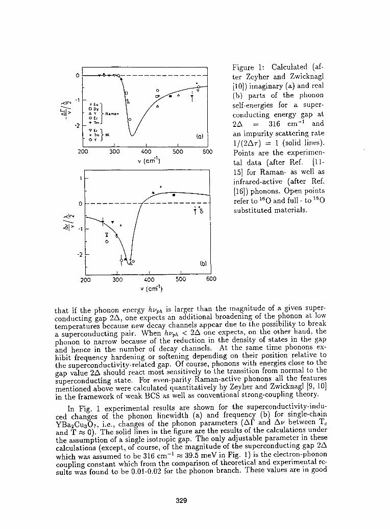
Figure 1: Calculated (af-0 _o_ ter Zeyher and Zwicknagl
o_----_/'_'_ f [10]) imaginary (a) and real._-1 (b) parts of the phonon
/_l > - _' R.m.° self-energies for a super-
, e, conducting energy gap at0 TmJ-2 + 2A = 316 cm -1 and
°,:}E*
- ,a (ol an impurity scattering rate- 0
, , , 1/(2At) = 1 (solid lines).200 300 _oo 500 6oo Points are the experimen-
v (cmq) tal data (after Ref. [11-
1- 15] for Raman- as well asinfrared-active (after Ref.
[16])phonons. Open points0 refer to 160 and full - to 1so
-_1_ T6 substituted materials./+% iN
f t I
200 300 400 500 600
v (era-1)
that if the phonon energy huph is larger than the magnitude of a given super-conducting gap 2A, one expects an additional broadening of the phonon at lowtemperatures because new decay channels appear due to the possibility to breaka superconducting pair. When ht,ph < 2A one expects, on the other hand, thephonon to narrow because of the reduction in the density of states in the gapand hence in the number of decay channels. At the same time phonons ex-hibit frequency hardening or softening depending on their position relative tothe superconductivity-related gap. Of course, phonons with energies close to thegap value 2A should react most sensitively to the transition from normal to thesuperconducting state. For even-parity Raman-active phonons all the featuresmentioned above were calculated quantitatively by Zeyher and Zwicknagl [9, 10]in the framework of weak BCS as well as conventional strong-coupling theory.
In Fig. 1 experimental results are shown for the superconductivity-indu-ced changes of the phonon linewidth (a) and frequency (b) for single-chainYBa2CuaOv, i.e., changes of the phonon parameters (zXFand At, between Tcand T _ 0). The solid lines in the figure are the results of the calculations underthe assumption of a single isotropic gap. The only adjustable parameter in thesecalculations (except, of course, of the magnitude of the superconducting gap 2Awhich was assumed to be 316 cm-1 _ 39.5 meV in Fig. 1) is the electron-phononcoupling constant which from the comparison of theoretical and experimental re-sults was found to be 0.01-0.02 for the phonon branch. These values are in good
329
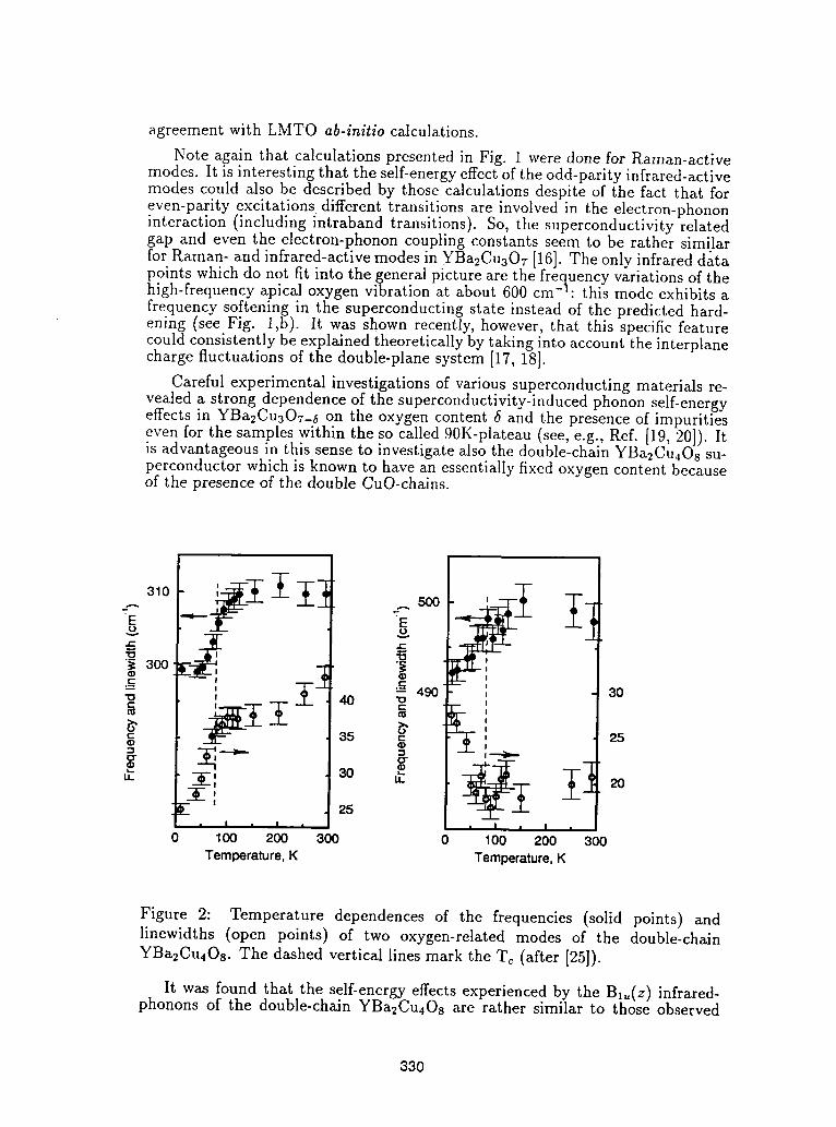
agreement with LMTO ab-initio calculations.
Note again that calculations presented in Fig. 1 were done for Raman-activemodes. It is interesting that the self-energy effect of the odd-parity infrared-activemodes could also be described by those calculations despite of the fact that foreven-parity excitations different transitions are involved in the electron-phononinteraction (including intraband transitions). So, the superconductivity relatedgap and even the electron-phonon coupling constants seem to be rather similarfor Raman- and infrared-active modes in YBa2Cu307 [16]. The only infrared datapoints which do not fit into the general picture are the frequency variations of thehigh-frequency apical oxygen vibration at about 600 cm-l: this mode exhibits afrequency softening in the superconducting state instead of the predicted hard-ening (see Fig. 1,b). It was shown recently, however, that this specific featurecould consistently be explained theoretically by taking into account the interplanecharge fluctuations of the double-plane system [17, 18].
Careful experimental investigations of various superconducting materials re-vealed a strong dependence of the superconductivity-induced phonon self-energyeffects in YBa_Cu3OT-8 on the oxygen content 6 and the presence of impuritieseven for the samples within the so called 90K-plateau (see, e.g., Ref. [19, 20]). Itis advantageous in this sense to investigate also the double-chain YBa2Cu40s su-perconductor which is known to have an essentially fixed oxygen content becauseof the presence of the double CuO-chains.
r-
= 300
_" 30 20
25
0 100 200 300 0 100 200 30_
Temperature,K Temperature,K
Figure 2: Temperature dependences of the frequencies (solid points) andlinewidths (open points) of two oxygen-related modes of the double-chainYBa2Cu4Os. The dashed vertical lines mark the Tc (after [25]).
It was found that the self-energy effects experienced by the Bl,,(z) infrared-phonons of the double-chain YBa2CuaOs are rather similar to those observed
330
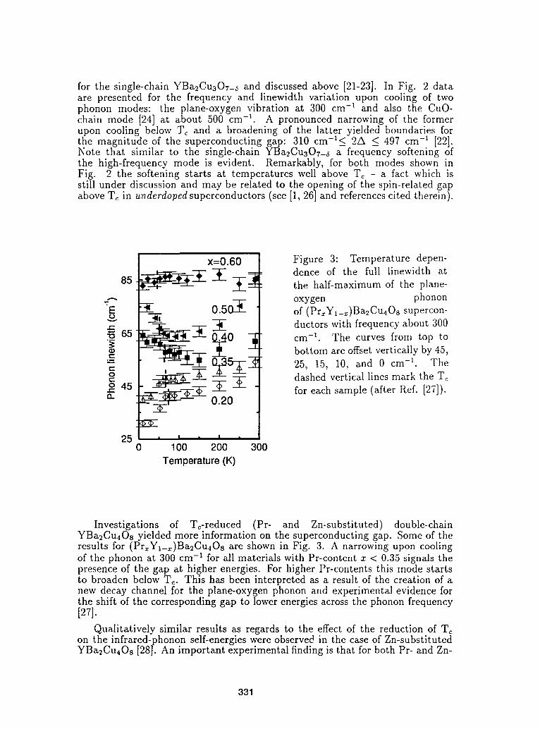
for the single-chain YBa2Cu3Or-s and discussed above [21-23]. In Fig. 2 dataare presented for the frequency and linewidth variation upon cooling of twophonon modes: the plane-oxygen vibration at 300 cm -_ and also the CuO-chain mode [24] at about 500 cm -l. A pronounced narrowing of the formerupon cooling below Tc and a broadening of the latter yielded boundaries forthe magnitude of the superconducting gap: 310 cm-l<_ 2A <_ 497 cm -1 [22].Note that similar to the single-chain YBa2Cu307_6 a frequency softening ofthe high-frequency mode is evident. Remarkably, for both modes shown inFig. 2 the softening starts at temperatures well above Tc - a fact which isstill under discussion and may be related to the opening of the spin-related gapabove Tc in underdoped superconductors (see [1, 26] and references cited therein).
x=0.60 Figure 3: Temperature depen-
85 "_--_--_-'-_-- _ X ff_ dence of the full linewidth atthe half-maximum of the plane-
oxygen phonon'E "-_ 0.50-._ of (Pr=Y___)Ba2Cu408 supercon-
_ -'_ ductors with frequency about 30065 _0 _ cm -1. The curves from top to
X - bottom are offset vertically by 45,._=
o 0__5-_2 25, 15, 10, and 0 cm -1. The,-- _-5[- T dashed vertical lines mark the T_--+-o 45 ._T_.
" '---,-_--_---_- for each sample (after Ref. [27])."_ _,'_'_ 0.20
25 , ' " ' "0 1O0 200 300
Temperature(K)
Investigations of T¢-reduced (Pr- and Zn-substituted) double-chainYBa2Cu40s yielded more information on the superconducting gap. Some of theresults for (Pr=Yl_=)Ba2Cu4Os are shown in Fig. 3. A narrowing upon coolingof the phonon at 300 cm -1 for all materials with Pr-content x < 0.35 signals thepresence of the gap at higher energies. For higher Pr-contents this mode startsto broaden below T_. This has been interpreted as a result of the creation of anew decay channel for the plane-oxygen phonon and experimental evidence forthe shift of the corresponding gap to lower energies across the phonon frequency[27].
Qualitatively similar results as regards to the effect of the reduction of T_on the infrared-phonon self-energies were observed in the case of Zn-substitutedYBa2Cu4Os [28]. An important experimental finding is that for both Pr- and Zn-
331
substitute different ions within the crystallographic structure) differs by factorof ten. As a comparison, there is no effect on the self-energies in the case ofSr substitution for Ba within a rather wide range of concentrations, which alsodoes not influence the superconducting temperature To. All these facts provideconvincing evidence that the discussed effects of the infrared-active phonon ofY2Ba4Cus+,_Oa4+n-_ are indeed superconductivity related.
Acknowledgments This work was supported by the Swedish ResearchBoard for Natural Sciences, the Bundesminister fiir Forschung und Technologicunder contract No. 13N5840 5 (Federal Republic of Germany) and the EuropeanCommunity. Part of this work was performed by one of us (A.P.L.) under the sup-port from the Swedish Superconductivity Consortium, Max-Planck Gesselschaft(Miinchen, Federal Republic Germany) and Alexander von Humboldt Founda-tion (Bonn, Federal Republic Germany). He also acknowledges the hospitality ofthe Max-Planck-Institut fiir FestkSrperforschung (Stuttgart, Federal Republic ofGermany) where part of this work was performed.
References
[1] A.P. Litvinchuk, C. Thomsen, and M. Cardona, in Physical Properties ofHigh Temperature Superconductors IV, ed. by D.M. Ginsberg (World Scien-tific, Singapore, 1994), p.375.
[2] D.B. Tanner and T. Timusk in Physical properties of High Temperature Su-perconductors III, ed. by D.M. Ginsberg (World Scientific, Singapore, 1992),p.363.
[3] K.F. Renk, in: Tl-based High Temperature Superconductors, ed. by A.H.Hermann and J.V. Yakhmi (Marcel Dekker, Inc., Publishers, New York,1992), p.477.
[4] C. Thomsen, in Light Scattering in Solids VI, ed. by M. Cardona and G.Gfintherodt (Springer, Berlin, Heidelberg, New York, 1991), p.285.
[5] R. Feile, Physica C 159, 1 (1989).
[6] R.M. Macfarlane, H.J. Rosen, and H. Seki, Solid State Commun. 63, 831(1987).
[7] A. Wittlin, R. Liu, M. Cardona, L. Genzel, W. KSnig, W. Bauhofer, Hj.Mattausch, A. Simon, and F. Garcia-Alvarado, Solid State Commun. 64,477 (1987).
[8] T. Zetterer, M. Franz, J. Schfitzmann, W. Ose, H.H. Otto, and K.F. Renk,Solid State Commun. 75, 325 (1990).
[9] R. Zeyher and G. Zwicknagl, Solid State Commun. 66, 617 (1988).
[10] R. Zeyher and G. Zwicknagl, Z. Phys. B: Condensed Matter 78, 175 (1990).
[11] B. Friedl, C. Thomsen, and M. Cardona. Phys. Rev. Lett. 65,915 (1990).
[12] C. Thomsen, M. Cardona, B. Friedl, C.O. Rodriguez, I.I. Mazin, andO.K. Andersen, Solid State Commun. 75, 219 (1990).
332
[13] B. Friedl, C. Thomsen, H.-U. Habermeier, and M. Cardona, Solid StateCommun. 78,291 (1991).
[14] B. Friedl, C. Thomsen, E. SchSnherr, and M. Cardona, Solid State Commun.76, 1107 (1990).
[15] B. Friedl, PhD. Thesis, Universit£t Stuttgart, 1992.
[16] A.P. Litvinchuk, C. Thomsen, and M. Cardona, Solid State Commun. 80,257 (1991).
[17] G. Hastreiter and J. Keller, Solid State Commun. 85,967 (1993).
[18] G. Hastreiter, F. Forsthofer, and J. Keller, Solid State Commun. 88, 769(1993).
[19] C. Thomsen, B. Friedl, M. Cieplak, and M. Cardona, Solid State Commun.78, 727 (1991).
[20] E. Altendorf, J.C. Irwin, R. Liang, and W.N. Hardy, Phys. Rev. B 45, 7551(1992).
[21] A.P. Litvinchuk, C. Thomsen, and M. Cardona, in Sixteenth Intern. Conf.on Infrared and Millimeter Waves, ed. by Siegrist, M.R., Tran M.Q., andTran T.M.: Proc. SPIE 1576, 22 (1991).
[22] A.P. Litvinchuk, C. Thomsen, P. Murugaraj, and M. Cardona, Z. Phys. B:Condensed Matter 86, 329 (1992).
[23] A.P. Litvinchuk, C. Thomsen, M. Cardona, J. Karpinski, E. Kaldis, andS. Rusiecki, Z. Phys. B: Condensed Matter 92, 9 (1993).
[24] C. Thomsen, A.P. Litvinchuk, E. SchSnherr, and M. Cardona, Phys. Rev.B 45, 8154 (1992).
[25] A.P. Litvinchuk, C. Thomsen, and M. Cardona, unpublished.
[26] A.P. Litvinchuk, C. Thomsen, and M. Cardona, Solid State Commun. 83,343 (1992).
[27] A.P. Litvinchuk, C. Thomsen, M. Cardona, L. BSrjesson, M. K£11, P. Be-rastegui, and L.-G. Johansson, Solid State Commun. 87, 907 (1993).
[28] A.P. Litvinchuk, C. Thomsen, M. Cardona, L. BSrjesson, P. Berastegui, andL.-G. Johansson, Phys. Rev. B 50, July, 1 (1994).
333


Physical Properties
Session PP-2 Chair: Prof. Valeri OzhoginCo-Chair. D. Brinkman

FLUX PINNING CHARACTERISTICS AND
IRREVERSIBILITY LINE IN HIGH TEMPERATURE
SUPERCONDUCTORS
T. Matsushita, N. Ihara and M. Kiuchi
Department of Computer Science and Electronics, Kyushu Institute of Technology,
680-4 Kawazu, Iizuka 820, Japan
ABSTRACT
The flux pinning properties in high temperature superconductors are strongly influenced by ther-mally activated flux motion. The scaling relation of the pinning force density and the irreversibilityline in various high temperature superconductors are numerically analyzed in terms of the flux creepmodel. The effect of two factors, i.e., the flux pinning strength and the dimensionality of the ma-terial, on these properties are investigated. It is speculated that the irreversibility line in Bi-2212superconductors is one order of magnitude smaller than that in Y-123, even if the flux pinningstrength in Bi-2212 is improved up to the level of Y-123. It is concluded that these two factors areequally important in determination of the flux pinning characteristics at high temperatures.
INTRODUCTION
The critical current density Jc is one of the most important parameters of high temperaturesuperconductors in their application to various fields. However, the critical current density inthese materials is empirically known to be significantly degraded with increasing magnetic fieldat high temperatures. Such a poor critical current property is ascribed to weak pinning strengthin these materials and large thermal activation of fluxoids at high temperatures. The boundarybetween the magnetically irreversible region with nonzero Jc and the reversible region with zeroJ¢ in the field(B)-temperature(T) plane is called the irreversibility line. The poor critical currentproperty in high temperature superconductors is directly concerned with their low irreversibilityline.
In order to quantitatively understand the critical current property at high temperatures, it isnecessary to take into account the effect of the thermally activated fluxoid motion correctly. Forthis purpose the collective flux creep theory [1] seems to be useful. One of the important features ofthis theory is that the pinning potential Uo can be estimated in terms of the virtual critical currentdensity Jco in the creep-free case. The theoretical result of the summation of elementary pinningforces is applicable to this quntity for a superconductor with known pinning centers. On the otherhand, in the case of unknown pinning centers as in most high temperature superconductors, thecritical current density observed at sufficiently low temperatures where the thermal activation is notsignificant can be approximately used as J¢0. The irreversibility lines in various superconductorscan be explained satisfactorily with respect to the dependences on temperature, flux pinningstrength and superconducting materials [2]. Therefore, the flux pinning characteristics in thevicinity of the irreversibility line can also be expected to be analysed correctly in terms of the fluxcreep theory. In this paper theoretical results on various superconductors are discussed and thescaling laws of the pinning force density are compared with experimental results.
THEORY
According to the flux creep nmdel [3], the induced electric field due to the thermally activated
337
fluxoid motion is given by
where a is the hopping distance of the flux bundle, g is the oscillation frequency of the flux bundlein the pinning potential, U is the activation energy caused by flux pinning and kB is the Boltzmannconstant. The factor of the exponential term gives the probability for flux bundle to jump overthe energy barrier due to the thermal activation. From the fact that the situation changes almostperiodically with respect to the displacement of fluxoids by their mean spacing af, it is expectedthat a can be approximately replaced by af. According to the theoretical analysis using theFokker-Planck equation [4], the oscillation frequency is given by
_PfJcOu = 2_raf-----B' (2)
where ff is a constant dependent on the pinning center and takes 21r for point defects [5] and pf isthe flow resistivity.
The activation energy U varies when the current density J varies and its variation depends on theshape of the pinning potential. If we assume a sinusoidally varying washboard pinning potential,U is written as
U(j) = U0[(1 - j2)1/2 _ jcos-lj], (3)
where j = J/Jco is the reduced current density.
According to the flux creep theory [1] the pinning potential Uo in bulk superconductors is expressedas
Uo = 0"83592kBJ1/°2_3/2B1/4 , (4)
where g2 is the number of fluxoids in the flux bundle. In the original flux creep theory [1], thenumber g2 was expected to be determined by the elastic correlation length as
g2 -- C66af 2J-ZoB--g°' (5)
where C66 is the shear modulus of the fluxoid lattice. However, it has been clarified [61 that thepractical g2 values estimated from the observed irreversibility field are smaller than g[ given byEq. (5). This tendency is more remarkable for the larger g2 value and for the case of the magneticfield parallel to the c-axis [7, 8]. This behavior can be understood as the result of the irreversiblethermodynamics so as to minimize the energy dissipation. That is, if the flux bundle size becomessmaller, the flexibility of fluxoids to be pinned by distributed pinning centers increases, resultingin the stronger pinning, while it leads to the smaller pinning potential due to smaller volume,resulting in the larger effect of thermal activation. Thus, the optimal condition exists and g2 isexpected to be given by [7]
rskT.= g2 \ Ec ]J ' (6)
where Ue is the virtual pinning potential when g2 is equal to g2 and Ec is the electric field criterionfor the definition of the critical current density.
In the case of magnetic field normal to the c-axis, g2 is proportional to the coherence length alongthe c-axis. Hence, the flux bundle tends to have small sizes in two-dimensional superconductors.For the magnetic field parallel to the c-axis, the corresponding coherence length is that in the a-bplane, and the obtained Ue is very large. However, this results in quite small g2 value from Eq.(6) [8]. It is concluded, therefore, that the two-dimensional superconductors are more stronglyinfluenced by the thermal activation in the both field directions.
338
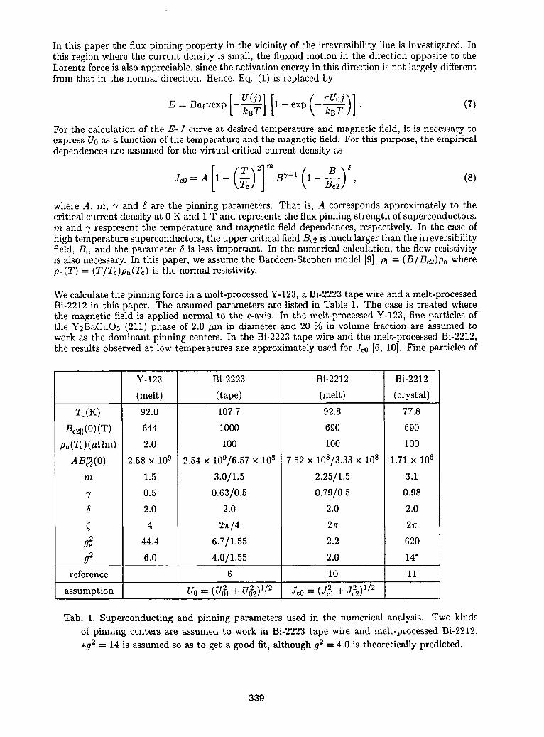
In this paper the flux pinning property in the vicinity of the irreversibility line is investigated. Inthis region where the current density is small, the fluxoid motion in the direction opposite to theLorentz force is also appreciable, since the activation energy in this direction is not largely differentfrom that in the normal direction. Hence, Eq. (1) is replaced by
[ (J)l[E = Bafuexp L- k----B'--BTI1 -- exp \ ksT ]J " (7)
For the calculation of the E-J curve at desired temperature and magnetic field, it is necessary toexpress Uo as a function of the temperature and the magnetic field. For this purpose, the empiricaldependences are assumed for the virtual critical current density as
Jco=A 1- _ B "r-1 1-_ , (8)
where A, m, 7 and 5 are the pinning parameters. That is, A corresponds approximately to thecritical current density at 0 K and 1 T and represents the flux pinning strength of superconductors.m and 7 respresent the temperature and magnetic field dependences, respectively. In the case ofhigh temperature superconductors, the upper critical field B¢2 is much larger than the irreversibilityfield, Bi, and the parameter 5 is less important. In the numerical calculation, the flow resistivityis also necessary. In this paper, we assume the Bardeen-Stephen model [9], pf = (B/B_2)p, wherepn(T) = (T/Tc)p,(Tc) is the normal resistivity.
We calculate the pinning force in a melt-processed Y-123, a Bi-2223 tape wire and a melt-processedBi-2212 in this paper. The assumed parameters are listed in Table 1. The case is treated wherethe magnetic field is applied normal to the c-axis. In the melt-processed Y-123, fine particles ofthe Y2BaCuO5 (211) phase of 2.0 /zm in diameter and 20 % in volume fraction are assumed towork as the dominant pinning centers. In the Bi-2223 tape wire and the melt-processed Bi-2212,the results observed at low temperatures are approximately used for J¢0 [6, 10]. Fine particles of
Y-123 Bi-2223 Bi-2212 Bi-2212
(melt) (tape) (melt) (crystal)
To(K) 92.0 107.7 92.8 77.8
B¢211(0)(T) 644 i000 690 690
pn(T¢) (/zf2m) 2.0 I00 I00 i00
ABe(O) 2.58x 10⁹ 2.54x 10⁹/6.57x 108 7.52x 10⁸/3.33x 108 1.71X 10⁶
m 1.5 3.0/1.5 2.25/1.5 3.1
7 0.5 0.63/0.5 0.79/0.5 0.98
6 2.0 2.0 2.0 2.0
4 2_/4 27r 2_
92 44.4 6.7/1.55 2.2 620
92 6.0 4.0/1.55 2.0 14"
reference 6 10 11
assumption Uo = (U21 nt" U22) 1/2 J¢o -- (J21 + J22)1/2
Tab. 1. Superconducting and pinning parameters used in the numerical analysis. Two kinds
of pinning centers are assumed to work in Bi-2223 tape wire and melt-processed Bi-2212.
.g2 __ 14 is assumed so as to get a good fit, although g2 = 4.0 is theoretically predicted.
339
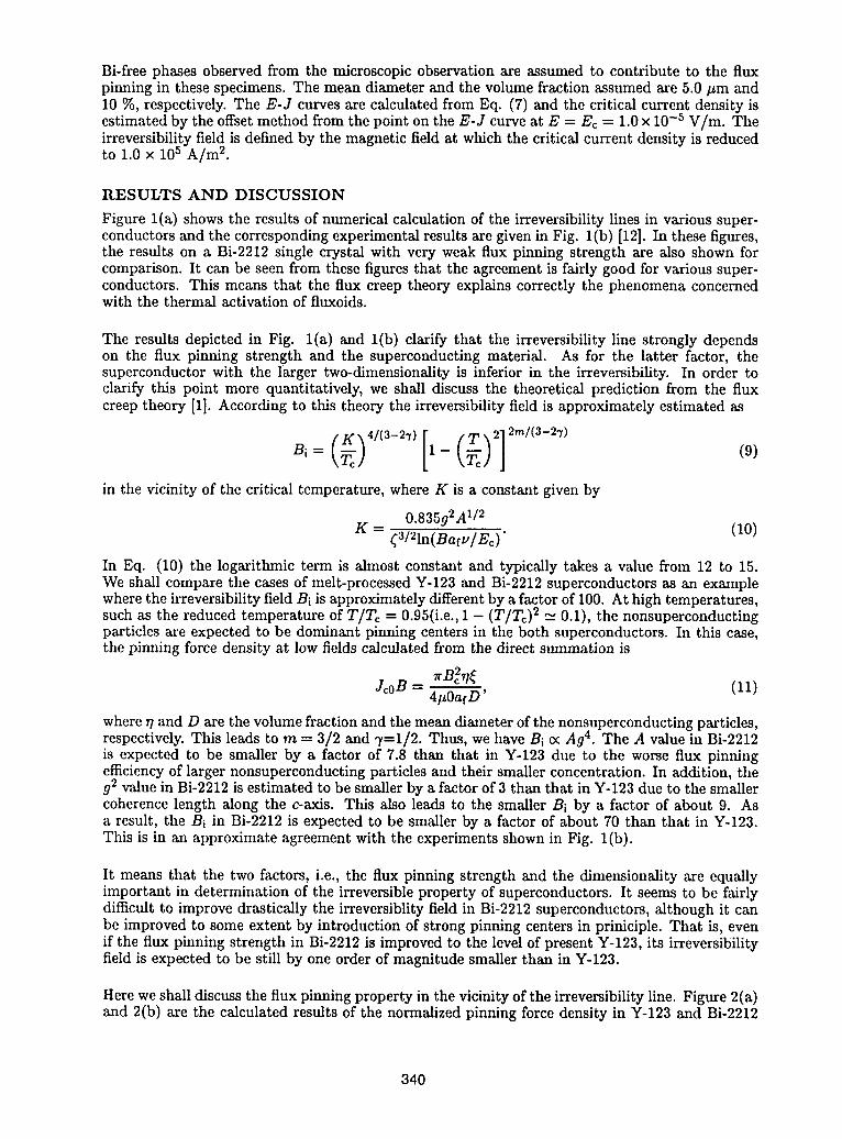
Bi-free phases observed from the microscopic observation are assumed to contribute to the fluxpinning in these specimens. The mean diameter and the volume fraction assumed are 5.0 pm and10 %, respectively. The E-J curves are calculated from Eq. (7) and the critical current density isestimated by the offset method from the point on the E-J curve at E -- E¢ = 1.0 × 10⁻⁵ V/m. Theirreversibility field is defined by the magnetic field at which the critical current density is reducedto 1.0 x 10⁵ A/m 2.
RESULTS AND DISCUSSION
Figure l(a) shows the results of numerical calculation of the irreversibility lines in various super-conductors and the corresponding experimental results are given in Fig. l(b) [12]. In these figures,the results on a Bi-2212 single crystal with very weak flux pinning strength are also shown forcomparison. It can be seen from these figures that the agreement is fairly good for various super-conductors. This means that the flux creep theory explains correctly the phenomena concernedwith the thermal activation of fluxoids.
The results depicted in Fig. l(a) and l(b) clarify that the irreversibility line strongly dependson the flux pinning strength and the superconducting material. As for the latter factor, thesuperconductor with the larger two-dimensionality is inferior in the irreversibility. In order toclarify this point more quantitatively, we shall discuss the theoretical prediction from the fluxcreep theory [1]. According to this theory the irreversibility field is approximately estimated as
in the vicinity of the critical temperature, where K is a constant given by
K =. 0"835g2AU2_3/21n(Bafu / E¢) . (10)
In Eq. (10) the logarithmic term is almost constant and typically takes a value from 12 to 15.We shall compare the cases of melt-processed Y-123 and Bi-2212 superconductors as an examplewhere the irreversibility field Bi is approximately different by a factor of 100. At high temperatures,such as the reduced temperature of T/Tc = 0.95(i.e., 1 - (T/Tc) 2 _ 0.1), the nonsuperconductingparticles are expected to be dominant pinning centers in the both superconductors. In this case,the pinning force density at low fields calculated from the direct summation is
rB2T/_
JcoB = 41_0afD' (11)
where 77and D are the volume fraction and the mean diameter of the nonsuperconducting particles,respectively. This leads to m ---3/2 and 7--1/2. Thus, we have Bi ¢xAg 4. The A value in Bi-2212is expected to be smaller by a factor of 7.8 than that in Y-123 due to the worse flux pinningefficiency of larger nonsuperconducting particles and their smaller concentration. In addition, theg2 value in Bi-2212 is estimated to be smaller by a factor of 3 than that in Y-123 due to the smallercoherence length along the c-axis. This also leads to the smaller Bi by a factor of about 9. Asa result, the Bi in Bi-2212 is expected to be smaller by a factor of about 70 than that in Y-123.This is in an approximate agreement with the experiments shown in Fig. 1(b).
It means that the two factors, i.e., the flux pinning strength and the dimensionality are equallyimportant in determination of the irreversible property of superconductors. It seems to be fairlydifficult to improve drastically the irreversiblity field in Bi-2212 superconductors, although it canbe improved to some extent by introduction of strong pinning centers in priniciple. That is, evenif the flux pinning strength in Bi-2212 is improved to the level of present Y-123, its irreversibilityfield is expected to be still by one order of magnitude smaller than in Y-123.
Here we shall discuss the flux pinning property in the vicinity of the irreversibility line. Figure 2(a)and 2(b) are the calculated results of the normalized pinning force density in Y-123 and Bi-2212
340
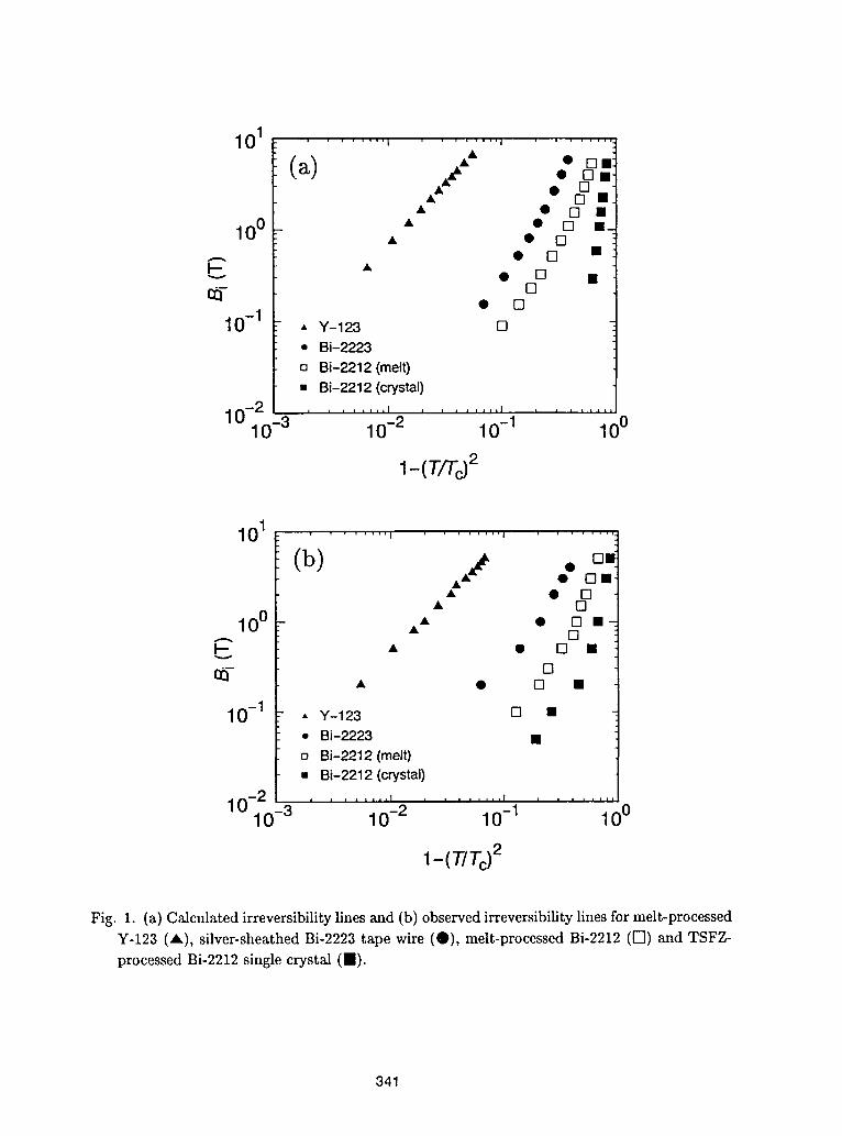
-,-UU1 ....... ...... , ........ :
(b) / • o.• • Om• • 0
• []-gn0 • • [] •IU
• []F-- • • [] •
_- []• • [] •
10-1 ,, Y-123 [] •
• Bi-2223 •o Bi-2212 (melt)• Bi-2212 (crystal)
120 ........ ' ........ ' ....... 0010
-3 1Au-2 1nu-1 1
1-(T/Tc)2
Fig. 1. (a) Calculated irreversibility lines and (b) observed irreversibility lines for melt-processed
Y-123 (A), silver-sheathed Bi-2223 tape wire (O), melt-processed Bi-2212 ([[]) and TSFZ-
processed Bi-2212 single crystal (m).
341
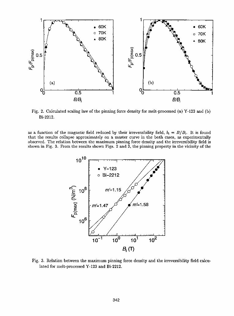
% o7oK
B/_ B/B i
Fig. 2. Calculated scaling law ofthe pinmngforce density formelt-processed (a) Y-123and (b)Bi-2212.
as a function of the magnetic field reduced by their irreversibility field, bi = B/Bi. It is foundthat the results collapse approximately on a master curve in the both cases, as experimentallyobserved. The relation between the maximum pinning force density and the irreversibility field isshown in Fig. 3. From the results shown Figs. 2 and 3, the pinning property in the vicinity of the
10lo
_'_"108Z
Ev
u?-106
10 -1 10° 101 10 2
a,(m)
Fig. 3. Relation between the maximum pinning force density and the irreversibility field calcu-lated for melt-processed Y-123 and Bi-2212.
342
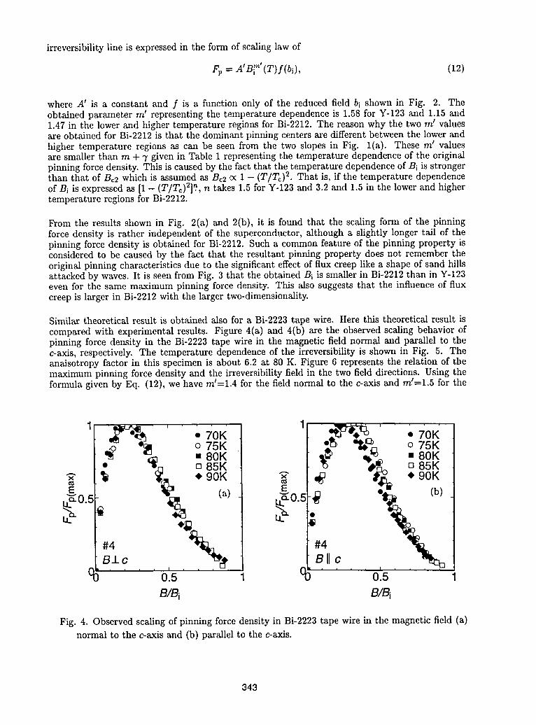
irreversibility line is expressed in the form of scaling law of
Fp = A'B_' (T)f(bi), (12)
where A_ is a constant and f is a function only of the reduced field bi shown in Fig. 2. Theobtained parameter m _ representing the temperature dependence is 1.58 for Y-123 and 1.15 and1.47 in the lower and higher temperature regions for Bi-2212. The reason why the two m _ valuesare obtained for Bi-2212 is that the dominant pinning centers are different between the lower andhigher temperature regions as can be seen from the two slopes in Fig. l(a). These m _ valuesare smaller than m + 7 given in Table 1 representing the temperature dependence of the originalpinning force density. This is caused by the fact that the temperature dependence of Bi is strongerthan that of Be2 which is assumed as Be2 (x 1 - (T/To) 2. That is, if the temperature dependenceof Bi is expressed as [1 - (T/Tc)2]n., n takes 1.5 for Y-123 and 3.2 and 1.5 in the lower and highertemperature regions for Bi-2212.
From the results shown in Fig. 2(a) and 2(b), it is found that the scaling form of the pinningforce density is rather independent of the superconductor, although a slightly longer tail of thepinning force density is obtained for Bi-2212. Such a common feature of the pinning property isconsidered to be caused by the fact that the resultant pinning property does not remember theoriginal pinning characteristics due to the significant effect of flux creep like a shape of sand hillsattacked by waves. It is seen from Fig. 3 that the obtained Bi is smaller in Bi-2212 than in Y-123even for the same maximum pinning force density. This also suggests that the influence of fluxcreep is larger in Bi-2212 with the larger two-dimensionality.
Similar theoretical result is obtained also for a Bi-2223 tape wire. Here this theoretical result iscompared with experimental results. Figure 4(a) and 4(b) are the observed scaling behavior ofpinning force density in the Bi-2223 tape wire in the magnetic field normal and parallel to thec-axis, respectively. The temperature dependence of the irreversibility is shown in Fig. 5. Theanaisotropy factor in this specimen is about 6.2 at 80 K. Figure 6 represents the relation of themaximum pinning force density and the irreversibility field in the two field directions. Using theformula given by Eq. (12), we have m_=l.4 for the field normal to the c-axis and m_=1.5 for the
1 '.-_' ' " 70K 1l '__' " " 70K,o'= _m, o 75K I _'15 '_o.L_ o 75K'_ _ • 80K I al# _,_ • 80K• -'l_ u 85K t _' _ u 85K
-'' -o% #4#4 fBII c '_s,±c, , , , , ,0.5 °5 '0'.s....
B/B_ B/_
Fig. 4. Observed scaling of pinning force density in Bi-2223 tape wire in the magnetic field (a)
normal to the c-axis and (b) parallel to the c-axis.
343
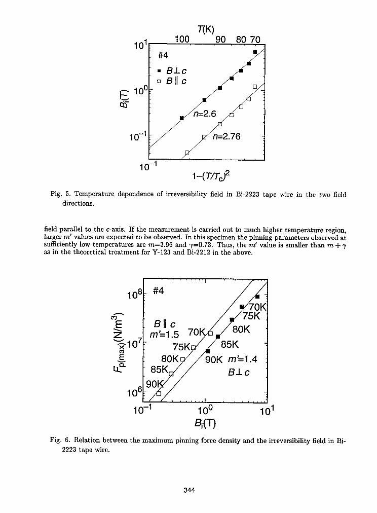
T(K)•,1 100 90 80 701U
/m• B.Lc[] e llc _"
1°°n=2 76
i i
10-1I-(T/Tc)2
Fig. 5. Temperature dependence of irreversibility field in Bi-2223 tape wire in the two fielddirections.
field parallel to the c-axis. If the measurement is carried out to much higher temperature region,larger rn_values are expected to be observed. In this specimen the pinning parameters observed atsufficiently low temperatures are m=3.96 and 7=0.73. Thus, the m _value is smaller than rn + 7as in the theoretical treatment for Y-123 and Bi-2212 in the above.
108
106
10-1 10° 101_(T)
Fig. 6. Relation between the maximum pinning force density and the irreversibility field in Bi-2223 tape wire.
344
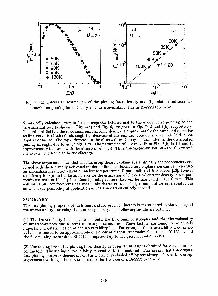
1..... tlo9............#4 (b)
Ic B.Lc
z 90K/r/• '-'0 =
_107 m'--1.20
, 61 / ........ i , • .....°6 ' o.s 1 1to-1 lo0 o'
B/Bi
Fig. 7. (a) Calculated scaling law of the pinning force density and (b) relation between the
maximum pinning force density and the irreversibility line in Bi-2223 tape wire.
Numerically calculated results for the magnetic field normal to the c-axis, corresponding to theexperimental results shown in Fig. 4(a) and Fig. 6, are given in Fig. 7(a) and 7(b), respectively.The reduced field at the maximum pinning force density is approximately the same and a similarscaling curve is obtained, although the decrease of the pinning force density at high field is notlarge as observed. The rapid decrease in the observed result may be attributed to the distributedpinning strength due to inhomogeneity. The parameter m' obtained from Fig. 7(b) is 1.2 and isapproximately the same with the observed m' = 1.4. Thus, the agreement between the theory andthe experiment seems to be satisfactory.
The above argument shows that the flux creep theory explains systematically the phenomena con-cerned with the thermally activated motion of fluxoids. Satisfactory explanation can be given alsoon anomalous magnetic relaxation at low temperatures [7] and scaling of E-J curves [13]. Hence,this theory is expected to be applicable for the estimation of the critical current density in a super-conductor with artificially introduced pinning centers that will be fabricated in the future. Thiswill be helpful for foreseeing the attainable characteristics of high temperature superconductorson which the possibility of application of these materials entirely depend.
SUMMARY
The flux pinning property of high temperature superconductors is investigated in the vicinity ofthe irreversibility line using the flux creep theory. The following results are obtained:
(1) The irreversibility line depends on both the flux pinning strength and the dimensionalityof superconductors due to their anisotropic structures. These factors are found to be equallyimportant in determination of the irreversibility line. For example, the irreversibility field in Bi-2212 is estimated to be approximately one order of magnitude smaller than that in Y-123, even ifthe flux pinning strength in Bi-2212 is improved up to the present level of Y-123.
(2) The scaling law of the pinning force density as observed usually is obtained for various super-conductors. The scaling curve is fairly insensitive to the material. This means that the originalflux pinning property dependent on the material is shaded off by the strong effect of flux creep.Agreements with experiments are obtained for the case of a Bi-2223 tape wire.
345
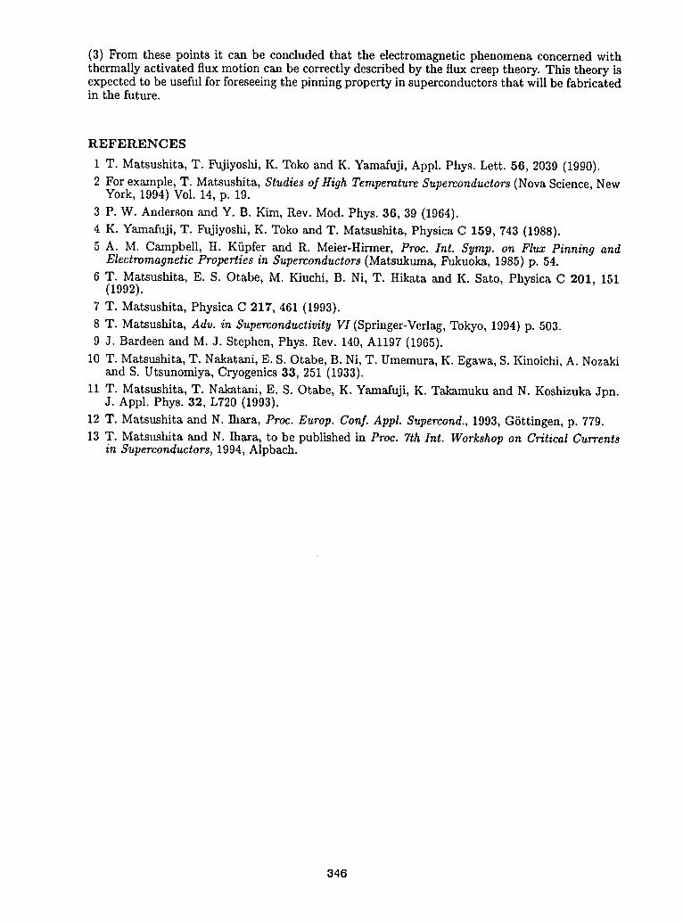
(3) From these points it can be concluded that the electromagnetic phenomena concerned withthermally activated flux motion can be correctly described by the flux creep theory. This theory isexpected to be useful for foreseeing the pinning property in superconductors that will be fabricatedin the future.
REFERENCES
1 T. Matsushita, T. Fujiyoshi, K. Toko and K. Yamafuji, Appl. Phys. Lett. 56, 2039 (1990).
2 For example, T. Matsushita, Studies o/High Temperature Superconductors (Nova Science, NewYork, 1994) Vol. 14, p. 19.
3 P. W. Anderson and Y. B. Kim, Rev. Mod. Phys. 36, 39 (1964).
4 K. Yamafuji, T. Fujiyoshi, K. Toko and T. Matsushita, Physica C 159, 743 (1988).
5 A. M. Campbell, H. Kfipfer and R. Meier-Hirmer, Proc. Int. Syrup. on Flux Pinning andElectromagnetic Properties in Superconductors (Matsukuma, Fukuoka, 1985) p. 54.
6 T. Matsushita, E. S. Otabe, M. Kiuchi, B. Ni, T. Hikata and K. Sato, Physica C 201, 151(1992).
7 T. Matsushita, Physica C 217, 461 (1993).
8 T. Matsushita, Adv. in Superconductivity VI (Springer-Verlag, Tokyo, 1994) p. 503.
9 J. Bardeen and M. J. Stephen, Phys. Rev. 140, Al197 (1965).
10 T. Matsushita, T. Nakatani, E. S. Otabe, B. Ni, T. Umemura, K. Egawa, S. Kinoichi, A. Nozakiand S. Utsunomiya, Cryogenics 33, 251 (1933).
11 T. Matsushita, T. Nakatani, E. S. Otabe, K. Yamafuji, K. Takamuku and N. Koshizuka Jpn.J. Appl. Phys. 32, L720 (1993).
12 T. Matsushita and N. Ihara, Proc. Europ. Conf. Appl. Supercond., 1993, GSttingen, p. 779.
13 T. Matsushita and N. Ihara, to be published in Proc. 7th Int. Workshop on Critical Currentsin Superconductors, 1994, Alpbach.
346
EFFECTS OF NEUTRON IRRADIATION ON THE LONDONPENETRATION DEPTH FOR POLYCRYSTALLINE
Bil.sPbo.3Sr2Ca2Cu3010 SUPERCONDUCTOR.
J. G. Ossandon,a J. R. Thompson, b'e Yang Ren Sun,b D. K. Christen, eand B. C. Chakoumakos.e
aFacultad de Recursos Naturales, Universidad de Talca, Talca, Chile,bDepartment of Physics, Univ. of Tennessee, Knoxville, TN 3 7996-1200, U.S.A.eOak Ridge National Laboratory, P. O. Box 2008, Oak Ridge, TN 37831-6061
ABSTRACT
Magnetization studies of polycrystalline Bil.sPbo.3Sr2Ca2Cu3010superconductor, prior to and after neutron irradiation, showed an increase inJe due to irradiation damage. Analysis of the equilibrium magnetizationrevealed significant increases in other more fundamental properties. Inparticular, the London penetration depth increased by -15 % followingirradiation with 8x10¹⁶neutrons/cm 2. Corresponding changes were observedin the upper critical magnetic field He2. However, the most fundamentalthermodynamic property, the superconductive condensation energy Fe, wasunaffected by the moderate level of neutron-induced damage.
INTRODUCTION
Magnetometricstudieshavebeenwidelyusedto determinethephysicalpropertiesof high temperature superconductors(HTSC).1 For example, the intragrainpersistentcurrent density Jp(T,H) in the mixed state can be found from measurementsof theirreversiblemagnetizationby meansof the Bean model,provided the grain morphologyis known. The Londonpenetrationdepth k can often be obtainedfrom the logarithmicslope of the equilibrium(reversible)magnetizationM(H,T) using the standardLondon-limit formalism of Kogan et al.2 More recent theoretical developments, however(Bulaevskiiet al.3, Kogan et al.4), have shown that vortexfluctuations are importantin regionsof magneticfieldand temperatureabovethe irreversibilityline, wherevorticesare free to moveto theirequilibriumlocations. In particular, theentropyassociatedwithfluctuationsintroduces a correctionto the equilibriumfree energy, which modifiesthe
347
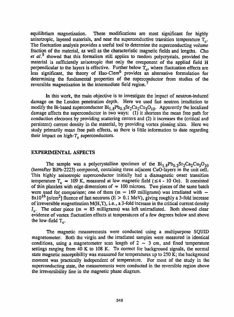
equilibrium magnetization. These modifications are most significant for highlyanisotropic, layered materials, and near the superconductivetransitiontemperature Tc.The fluctuationanalysisprovidesa useful tool to determinethe superconductingvolumefraction of the material, as well as the characteristicmagneticfields and lengths. Choet al.5 showed that this formalism still applies to random polycrystals, provided thematerial is sufficientlyanisotropic that only the component of the applied field Hperpendicularto the layersis effective. Further belowTe, where fluctuationeffects areless significant, the theory of Hao-Clem6 provides an alternative formulation fordetermining the fundamental properties of the superconductor from studies of thereversible magnetizationin the intermediatefield region.7
In this work, the main objective is to investigatethe impactof neutron-induceddamage on the London penetration depth. Here we used fast neutron irradiation tomodify the Bi-basedsuperconductorBil.sPbo.3Sr2Ca2Cu3010.Apparentlythe localizeddamageaffects the superconductorin two ways: (1) it shortensthe mean free path forconductionelectronsby providingscatteringcentersand (2) it increasesthe (criticalandpersistent) current density in the material,by providingvortexpinning sites. Here westudy primarily mean free path effects, as there is little informationto date regardingtheir impacton high-Te superconductors.
EXPERIMENTAL ASPECTS
The sample was a polycrystalline specimen of the Bil.sPb0.3Sr2Ca2Cu3010(hereafterBiPb-2223)compound,containingthree adjacentCuO-layersin the unit cell.This highly anisotropic superconductor initially had a diamagnetic onset transitiontemperatureTe = 109 K, measuredat low magneticfield (_<4 - 10 Oe). It consistedof thin plateletswith edgedimensionsof = 100microns. Two piecesof the samebatchwere used for comparison;one of them (m = 169 milligrams)was irradiated with -8x10¹⁶[n/cm2]fluenceof fastneutrons(E > 0.1 MeV), givingroughlya 3-foldincreaseof irreversiblemagnetizationM(I-I,T),i.e., a 3-foldincreasein the criticalcurrentdensityJc" The other piece (m = 85 milligrams)was left unirradiated. Both showed clearevidence of vortexfluctuationeffects at temperaturesof a few degreesbelowand abovethe low-fieldTe.
The magnetic measurements were conducted using a multipurpose SQUIDmagnetometer: Both the virgin and the irradiated sampleswere measuredin identicalconditions, using a magnetometer scan length of 2 - 3 cm, and fixed temperaturesettings ranging from 40 K to 108 K. To correct for background signals, the normalstatemagneticsusceptibilitywas measuredfor temperaturesup to 250K; the backgroundmoment was practically independent of temperature. For most of the study in thesuperconductingstate, the measurementswere conductedin the reversible region abovethe irreversibilityline in the magneticphase diagram.
348
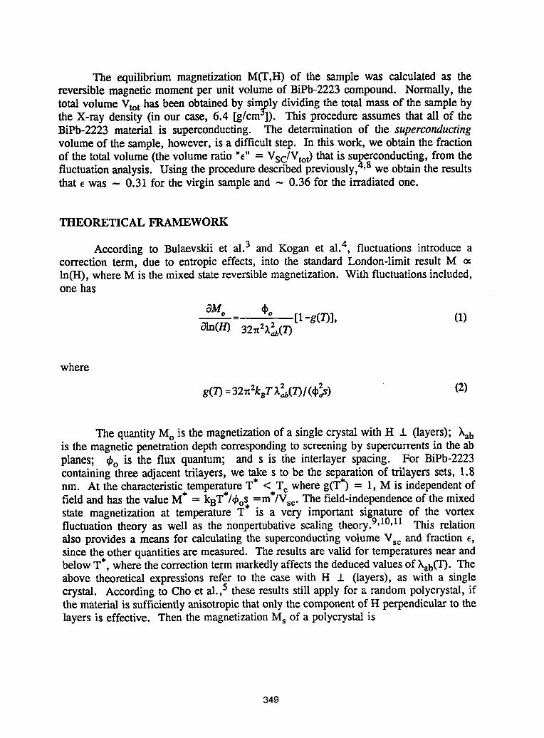
The equilibrium magnetizationM(T,H) of the sample was calculated as thereversible magneticmomentper unit volume of BiPb-2223compound. Normally, thetotal volume Vtot has been obtainedby sim,ply dividingthe total mass of the samplebythe X-ray density (in our case, 6.4 [g/cm°]). This procedure assumes that all of theBiPb-2223 material is superconducting. The determination of the superconductingvolume of the sample, however, is a difficultstep• In this work, we obtain the fractionof the total volume (the volumeratio "E" = Vsc/Vtot)that is superconducting,from thefluctuationanalysis. Using the proceduredescribedpreviously,4'8 we obtain the resultsthat Ewas - 0.31 for the virgin sampleand - 0.36 for the irradiated one.
THEORETICALFRAMEWORK
According to Bulaevskiiet al.3 and Kogan et al.4, fluctuations introduceacorrection term, due to entropiceffects, into the standardLondon-limitresult M ocin(H), where M is the mixed state reversible magnetization. With fluctuations included,one has
aMo dPo- [1-gCT)], (1)
ain(H)32 2x(73
where
g(T)=32_2knT)._(T)/ (_s) (2)
The quantityMo is the magnetizationof a singlecrystal with H .1.(layers); Xabis the magneticpenetrationdepthcorrespondingto screeningby supercurrentsin the abplanes; _o is the flux quantum; and s is the interlayer spacing. For BiPb-2223containingthree adjacent trilayers, we take s to be the separationof trilayers sets, 1.8
• • • • •
nm. At the characteristictemperatureT < Te where g(T*) = 1, M is independentoffield and has the value M* = kBT*/_bos=m*/Vsc.The field-independenceof the mixedstate magnettzaUonat temperature T is a very important s_gnatureof the vortexfluctuation theory as well as the nonpertubativescaling theory. 9'10'11 This relationalso provides a means for calculatingthe superconductingvolume Vse and fraction e,since the other quantitiesare measured. The resultsare valid for temperaturesnear andbelowT*, wherethe correctionterm markedlyaffects the deducedvalues of )_ab(T). Theabove theoretical expressions refer to the case with H .1. (layers), as with a singlecrystal. Accordingto Cho et al.,5 theseresults still apply for a random polycrystal,ifthe material is sufficientlyanisotropicthatonly the componentof H perpendicularto thelayers is effective. Then the magnetizationMs of a polycrystal is
349
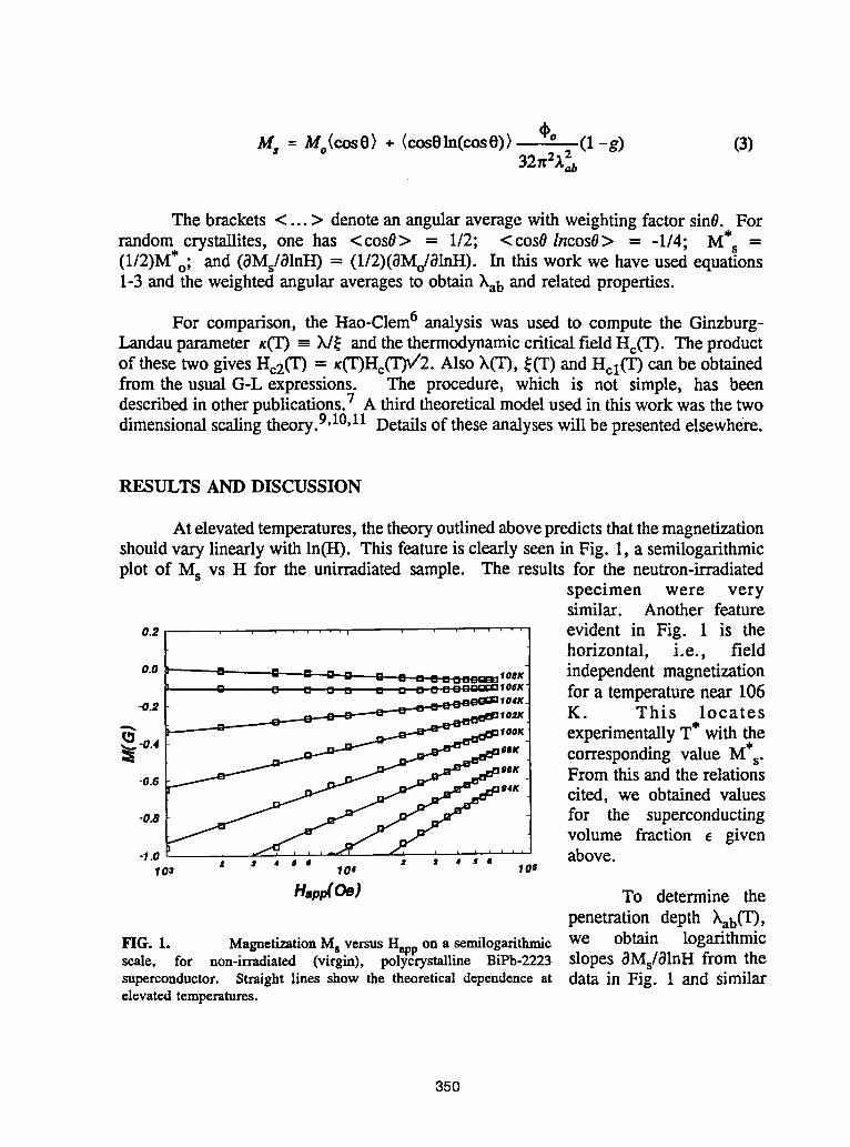
M, = uo(cose).(cose]n(cose))€o (1-g) (3)32n2_._
The brackets <... > denote an angular average with weighting factor sin0. Forrandom crystaUites, one has <cos0> = 1/2; <cos0 lncosO> = -1/4; M*s =(1/2)M*o; and (0Ms/01nH) = (1/2)(OMo/01nH). In this work we have used equations1-3 and the weighted angular averages to obtain )taband related properties.
For comparison, the Hao-Clem6 analysis was used to compute the Ginzburg-Landau parameter K(T) = k/_ and the thermodynamic critical field He(T). The productof these two gives Hc2(T) = K(T)He(T)v/2.Also X(T), _(T) and HcI(T) can be obtainedfrom the usual G-L expressions. The procedure, which is not simple, has beendescribed in other publications. 7 A third theoretical model used in this work was the twodimensional scaling theory. 9,10,11 Details of these analyses will be presented elsewhere.
RESULTS AND DISCUSSION
At elevatedtemperatures,thetheoryoutlinedabovepredictsthatthemagnetizationshouldvary linearlywith In(H). This featureis clearly seenin Fig. 1, a semilogarithmicplot of Ms vs H for the unirradiated sample. The results for the neutron-irradiated
specimen were verysimilar. Another feature
o._ ..... . evident in Fig. 1 is thehorizontal, ioe., field
o.o " -- -- :3 _............. ,,s,, independent magnetization" " 7."" ..--,,sK fo 106, o _ = z. _. r. . u ==---_-'_ r a temperaturenear
-o._ K. This locates
experimentallyT* wi_lVl_e-o.4 corresponding value s.-o.6 From this and the relations
cited, we obtained values-o.s for the superconducting
volume fraction e given-1.0 , , , ,, , , , ,, above.
lOS 10_ lOS
Hspp(Oe) To determine thepenetration depth Xab(T),
FIG. 1. Magnetization Ms versus Happ on a semilogarithmie we obtain logarithmicscale, for non-irradiated (virgin), polyerystalline BiPb-2223 slopes 0Ms/01nH from thesuperconductor. Straight lines show the theoretical dependence at data in Fig. 1 and similarelevated temperatures.
35O
0.4 plots. Analysis using Eq.1 and 2 with appropriateangular and volumetricfactors "_" leads directly to
•"_0.3 Xab for each isotherm.The results for the BiPb-::L 2223 virgin and irradiated
materials are summarizedin Fig. 2. The solid and_0.2dashed lines are BCStemperature dependenciesin the clean and dirty
o.1 limits, respectively, which45 55 65 75 85 95 105 were fitted to the data.
T (K) Points for T > T* (outsideof the range of validity ofthe theory) were not fitted.
FIG. 2. Xab(T)as a function of T from fluctuation analysis, From the BCS fits, thefor virgin and neutron irradiated BiPb-2223 materials. Dashed and extrapolated)_ab(0) and thesolid lines are BCS fits to the data in the clean and dirty limits, mean field transitionrespectively, temperature Tco,h(where X
diverges) are derived inboth limiting cases. In the more appropriate clean limit, the respective values are 139nm and 113.8 K for the unirradiated sample, compared with 152 nm and 112.9 K for theirradiated material. Observe that in each case, Tco,k lies several Kelvins above the lowfield diamagnetic onset T e values, 109 and 108 K, respectively. This is anothercharacteristic feature of the vortex fluctuation theory.
A central result of this study is the increase in London penetration depth k uponirradiation. Qualitatively, we attribute this feature to increased "dirtiness," i.e., disorderin the material, which scatters the conduction electrons. Another feature commonlyassociated with electron scattering and the associated reduction on electronic mean freepath is an increase in the slope of the upper critical magnetic field He2(T). Furtheranalysis using the Bulaevskii-Kogan formalism indeed revealed a substantial steepeningof the slope, by approximately 25-40 %. This increase was corroborated bycomplementary analyses using the Hao-Clem and scaling methods. An importantconsistency check is provided by the thermodynamic critical field He(0). This wascalculated both from the Hao-Clem formalism and from kab(0) and the coherence length_ab(0). We obtain nearly the same value, He(0) _- 1.3 T, for both the virgin and theirradiatedsamples. This result is consistent with the expectation that the superconductivecondensation energy Fe = He2/8z should not be affected by moderate densities ofneutron generated defects. Details will be presented elsewhere in a comprehensivediscussion.
351
CONCLUSION
Thisworkshowsthatneutron-generateddamageincreasedthe Londonpenetrationdepth of BiPb-2223superconductorby approximately10 - 15 %. Further analysisusingthree independenttheoreticalmodelshas shownthatHe2(0 ) concurrentlyincreasedby 25% - 40%. However, neither the thermodynamiccritical field He nor thetransitiontemperatureTe were appreciablyaffected. The observedbehavior is similarin magnitudeand directions to observations12in A-15 superconductors. For instance,Nb3Snand V3Si thin films with differingresidual resistivitiesjust above Te showedasignificantincrease in He2(0) (about _- 35 %) as the materialgoes from the clean (lowresistivity)limit to the dirty (highresistivity)limitat the expenseof a small decreaseinTc. The similarityof behavior suggeststhat the observedchanges for the BiPb-2223originate from mean free path effects. Further investigationsare under way to test thishypothesis.
We thank Carlos Becerra Labra and Walter Bussenius Cortada for theircollaboration.The work of J.G.O. was supportedby the ChileanNational ScienceandTechnologyFund (FONDECYTGrant N° 1930210)in cooperationwith the Universityof Talca. A portion of the work of J.R.T. and Y.R.S. was supportedby the ScienceAllianceof the Universityof Tennessee.The researchwas sponsoredby the DivisionofMaterialsSciences,U. S. DepartmentofEnergyand technologydevelopmentwas fundedby the U.S. Department of Energy, Office of Advanced Utilities Concepts-SuperconductorTechnologyProgram, both under ContractN° DE-AC-05-84OR21400with MartinMarietta EnergySystems, Inc.
REFERENCES
1. J.R. Thompson, D. K. Christen, H. R. Kerchner, L. A. Boatner, B. C. Sales,B. C. Chakoumakos, H. Hsu, J. Brynestad, D. M. Kroeger, J. W. Williams,Yang Ren Sun, Y. C. Kim, J. G. Ossandon, A. P. Malozemoff, L. Civale, A.D. Marwick, T. K. Worthington, L. Krusin-Elbaum, and F. Holtzberg, "Studiesof 'Non-Ideal' Superconductors using de Magnetic Methods," in MagneticSusceptibility of Superconductors and Other Spin Systems, ed. by R. A. Hein, T.Francavilla, and D. Liebenburg (Plenum, New York 1992), pp. 157-176.
2. V.G. Kogan, M. M. Fang, and Sreeparna Mitra, Phys. Rev. B 38, 11958(1988).
3. L.N. Bulaevskii, M. Ledvij, and V. G. Kogan, Phys. Rev. Lett. 68, 3773,(1992).
4. V.G. Kogan, M. Ledvij, A. Yu. Simonov, J. H. Cho, and D. C. Johnston,Phys. Rev. Lett. 70, 1870 (1993).
352
5. J.H. Cho, D. C. Johnston, M. Ledvij, and V. G. Kogan, Physica C 212, 419(1993).
6. Z. Hao, J. Clem, M. McElfresh, L. Civale, A. Malozemoff, and F. Holtzberg,Phys. Rev. B 43, 2844 (1991).
7. J.G. Ossandon, J. R. Thompson, D. K. Christen, B. C. Sales, H. R. Kerchner,J. O. Thomson, Y. R. Sun, K. W. Lay and J. E. Tkaczyk, Phys. Rev. B 45,12534 (1992).
8. J.R. Thompson, J. G. Ossandon, D. K. Christen, B. C. Chakoumakos, YangRen Sun, M. Paranthaman, and J. Brynestad, Phys. Rev. B (RC) 48, 14031(1993).
9. S. Ullah and A. T. Dorsey, Phys. Rev. B 44, 262 (1991).10. Z. Tesanovic, L. Xing, L. Bulaevskii, Qiang Li and M. Suenaga, Phys. Rev.
Lett. 69 3563 (1992). Also: Z. Tesanovic and A. V. Andreev, Phys. Rev. B,(accepted).
11. Qiang Li, K. Shibutani, M. Suenaga, I. Shigaki, and R. Ogawa, Phys. Rev. B 48,9877 (1993); Qiang Li, M. Suenaga, L. N. Bulaevskii, T. Hikata, and K. Sato,Phys. Rev. B 48, 13865 (1993).
12. T.P. Orlando, E. J. McNiff (Jr), S. Foner, and M. R. Beasley, Phys. Rev. B 19,4545 (1979).
353
THE THERMOPOWERIN THE TEMPERATURERANGETc-1000KANDTHE BANDSPECTRUMOF Bi-BASEDSUPERCONDUCTORS.
V.E.Gasumyants,E.V.Vladimirskaya,V.I.Smirnov,andS.V.Kazanskiy
State Technical University,St.Petersburg195257,Russia
The temperature dependenciesof thermopower,S, in the rangeT=Tc-1000Kas well as of resistivityand Hall coefficientin the range T=Tc-300K for thesingle-phaseceramicsamplesBi2Sr2Ca1xNdxCU2O, have been measured. Itwas foundthattheS(T) dependenciesinn_rmalphasYehavethreecharactedsticregions.Despite the fact that the S(T) dependenciesin Bi-based high-Tcsuperconductors(HTSC)differessentiallyfromonesinY-basedHTSC at T=Tc-300K, the main feature of theirs(S(T)=constat hightemperatures)retainsinsamplesinvestigatedat T>620K. The resultsobtainedhave been analyzedonthe basis of the narrow-bandmodel with the use of assumptionof slightasymmetryof the conductive band.The band spectrum parametersof thesamplesstudiedhave beencalculated.An analysisof the tendenciesin theseparameterschangeswith samplescompositionvarying enablesto make theconclusionaboutthe similarityof the main featuresof the conductive bandstructureinY- andBi-basedHTSC.
1. INTRODUCTION
it is hardto tell nowsomethingdefinitelyaboutthe bandstructurein Fermilevelvicinityof the Bi-basedHTSC. The complexexperimentalinvestigationof thetransportphenomenais oneof the mostavailablemethodforthe bandspectrumstudyand is reasonablyeffectiveoneat thesametime. Thisis confirmedconvincinglybythe expedenceonthe investigationsof semiconductorsand semimetalswith a complicatedelectronspectrum.The informationextractedfrom such an investigationbecomesmore detailedand unambiguousif we canvary the Fermi level positionovera widerangeof energy.Thisis usuallyachievedbydopingmaterialstudiedwith donororacceptorimpurities.
Earlierwe haveproposedthe phenomenologicalmodelof electrontransportinthe caseof narrowconduciveband[1].This so-callednarrowbandmodel has enabledus notonly toexplainall the specificfeaturesof transportcoefficientstemperaturedependencies,butalsoto determinethe bandspectrumparametersin the sampleswith differentcomposition.Onthe basis of analysisof tendenciesin these parameterschange we have made someconclusionsabout conductive band transformation character, influence of differentcomponentsof unit cell and have revealed the correlation between band spectrumparametersand criticaltemperature(Tc) value in the Y-basedHTSC [1-3]. To realize thisapproach,as appliedto the Bi-system,we havechosenthe 2212-phaseas a mainobject ofthe investigation.Comparedto the 2223-phasethis one is more stablethat enablesus topreparehighlydopedsamplesbeingsingle-phase.
It is knownthattemperaturedependenciesof resistivity(p)andHallcoefficient(R) in Bi-system are like the ones in Y-system (see, for example, [4]). However the S(T)dependenciesdifferessentiallyfromtheonesinY-basedHTSC [5,6]. It generatesa needforsomeadditionsto our modelfor explainingthesedependencies.On the otherhand dataabout Seebeck coefficient behaviorat T>300K are practicallyabsent in the literaturealthoughtheycan bequiteinformativeintheviewof bandspectrumstudying.
In this connection in this paper we carded out the experimentalinvestigationofthermopowerin Bi2Sr2Cal.xNdxCU2Oy(x=0-0.5) in the wide temperaturerange as well asanalysisof thenarrowbandmodelaplblicabilityto Bi-basedHTSC.
2. RESULTSAND DISCUSSION
354
The ceramicsamplesBi2Sr2Cal.xNdxCU2Oyhave been preparedby standardsolid-statesynthesismethodfrom high-purityoxidesandcarbonates.The absenceof heterogeneousphasesin the appreciableamountwas controlledby usingthe X-ray analysisas wellas bycomparative analysis of magneticsusceptibilityand transport coefficientstemperaturedependencies.
Table 1Thevaluesof transportcoefficientsin normalphaseandcriticaltemperaturein Bi2Sr2Cal.xNdxCU2Oy
x p(300K), p(100K), S(300K), R(30OK), Tcrn,K Tc°,Km_.cm m_.cm I_V/K x10-3cm3/C
0.0 1.2 0.6 -3.70 1.9 76.6 64.20.1 2.7 1.4 -2.08 2.9 83.9 66.00.2 3.0 2.0 2.17 4.2 82.6 56.90.3 3.5 2.9 6.30 6.8 75.9 53.90.4 3.8 3.7 15.82 9.6 56.0 34.20.5 11.1 9.4 31.10 12.5 36.0 23.5
The results of electro-physical measurementsare shown in Table 1. The Nd contentincrease leads to increasing of the absolutevalues of p, S, and R as well as Tc depressionand broadeningof superconductingtransition. The temperaturedependenciesof p and R aresimilar to the typical ones for all the HTSCmaterials.Dependenciesof p(T) are linear in allthe temperature range measured, the Hall coefficient decreases with the temperatureincrease,although the relative Iowedngof R for Bi-systemis not so great as for Y-system.
The S(T) dependencies are shown in Fig.l. These curves are stationary, i.e., they don'tchange after several temperaturecyclings. It can be seen from this figure that the absolutevalue of S increases with x and the S(T) dependencies in normal phase have threecharacteristic regions. At T=Tc-(120-200)Kthe thermopower have the smooth maximumwhich is charactedstic also to Y-system. At T=(120-200)K-620K one decreases almost
S, JxV/K8
1 • x-O.O
30 2 • =-0.1
"". S- zOl-.4. xOl
20 "• 5 • x-o.+I I
• IS • x-O.llI I
10 -,II I
o
-lO
0 200 400 600 800 1000T,K
Fig.1. The temperaturedependenciesof thermopowerin Bi2Sr2Cal.xNdxCU2Oy.
lineady which is charactedsticto Bi-based HTSC as comparedwith Y-based ones.Neverthelessthe mainfeatureof S(T) dependenciesinY-basedHTSC (S(T)=constat hightemperatures)retainsin Bi-basedHTSC at T>620K.The greatlengthof S lineardecreaseregion (300K) and very insignificantdeviationfrom S=constat high temperaturehaveengagedourattention.The lastfact is forcibleargumentin favor of the narrowbandmodelusing because its main consequenceis just independenceof S in the limit of high
355
temperature.Furthermore,yet anotherfact can be noted,This is the quitedrastictransitionfromsecondregionof S(T) dependenciesto thirdonewithindependenceof the temperatureof thistransition(T=620K)fromdopantcontent.It is necessaryto emphasizethat analogouspointof drastictransitionfrom onedependencetype to anotherwas beendetected byus inY-basedHTSC [7],althoughat anothertemperature(T=350K).It is possiblethat existingofthispointisa commonfeatureof differenttypesof HTSC.
For explanationand quantitativedescribingallthe experimentaldata obtainedwe mustbear in view the concrete model of band spectrumwith the lowest number of fittingparameters.For thispurposewe are using(as in the case of Y-basedHTSC) the narrow-bandmodelwhichsuggeststhe bandwidthto becomparablewiththe Fermismearing.Theanalysisof the main electrontransportpeculiaritiesin case of narrowbandis performedinRef.[1]. Certainof the conceptsandresultsof thisanalysisare asfollows.
The modelincludesthree phenomenologicalparameters.The firstoneis the degreeofbandfillingwith electronsthat isthe ratioof the free electronsnumberto the whole numberof bandstates.Two other parametersare the "statedensity"and "conductivity"effectivebandwidths (VVD and W_). These effective widths may differ from one anotheras well as
from the whole band width W. The distinctionsbetweenW, W D, W_ are relatedto thepeculiaritiesand differencesin energydependenciesof electronstate densityD(E) anddifferentialconductivity_(E). The comparisonof WD and W_ values may be used to getsome informationonthe electronkinetics,dynamicsandscatteringpeculiarities.As showninRef.[1], in the case of narrowband(i.e., when the W value is not much greaterthan koTvalue)thespectrumdetails,likethe D(E) and_(E) peculiarities,are notof greatsignificanceas longasthe WD andW_ values.This makespossibleto usethe simplestapproximationsfor these functionsas rectangleswith differentwidths. In this case we can derive theanalyticalexpressionsfor chemical potentialand all the transportcoefficients.It is to benoted that our formulas enabledus to compute the absolutevalue and the sign of theSeebeckcoefficientat the differenttemperatures,whereasthe p and R could be computedonlywithan accuracyof a constantcofactor.Thereforewe have usedS(T) dependenciestodetermine the model parametersvalues and then we have verified their validity bycomparisonbetweenthe calculatedandexperimentaldependenciesof the p(T)/p(30OK)andR(T)/R(300K). In the limitof hightemperature(whenWD<koT) Seebeckcoefficientdoesn'tdependontemperatureandis determinedfromformula:
S= k_.o.in Fe 1-F
It should be mentionedthat the fitting parametersare believed to be temperature-independent.That means thatthe parametersnumberis lessthan the numberof equationswhich we can use for their determinationbecause we compare the calculated andexperimentaltemperaturedependenciesina widetemperaturerange.
When analyzedthe transportcoefficientsinY-basedHTSC we have proposedthat theconductivebandis symmetric.For explanationof S(T) dependenciesin Bi-basedHTSC weuse narrowbandmodel too butwe add assumptionof slightasymmetryof the conductiveband. This fact is taken into account by introducingsome distance (b.WD, where b isasymmetryparameter)betweencentersof rectanglesD(E) and _(E). In this case all theformulas from Ref.[1] retain their previousform but in formulasfor transportcoefficientsinsteadof thechemicalpotentiali_we mustusenow(I_-b.WD).
In the frameworkof ourmodelwe were ableto describethetemperaturedependenciesof thermopowerin the wholetemperaturerangeadequately.The regionof drastictransitionS(T) from linear decrease to constant value is of particular complexity.The calculateddependenciesdemonstrateonly smooth transitionwhich may be due to roughnessofapproximationused.It is necessaryto take intoaccountthe featuresof the bandstructureinmore detail for the best agreement of experimentaland calculated dependencies.Inparticularit wouldappearreasonablethat the bandspectrumparametersare temperaturedependent.Nevertheless,analyzingthe resultsobtainedwe can considerwith reasonable
356
confidencethat our data lend supportto the validityof narrowband usingfor Bi-basedHTSC. It is necessaryto emphasizethat calculateddependenciesof p(T)and R(T) retainallitsfeaturesinthe frame of asymmetricmodel.
The dependenciesof the mainbandparameterscalculatedfromS(T) on Nd contentareshownin Fig.2. It can be seen that the deviationfrom stoichiometry(increaseof x inBi2Sr2Cal.xNdxCU2Ov)leadsto increaseof F value (the holedensitydecrease)as well as tothe appreciabletransformationof conductiveband. The effective band width graduallyincreaseswith x, in so doingthis broadeningof band is accompaniedby simultaneousreductionof W_/D ratio as shown by ourcalculations.Therefore,we couldassumethat
WD, meV F
400 0.49
300 0.48
200 0.47
100 0.46
0 0.460.0 0.1 0.2 0.@ 0.4 0.8
x
Fig.2. The bandeffectivewidthand the bandfillingdegreewithelectronsvs. Cacontent.
increase of dopant contentleads to the growth of the differencebetweenthe energydependenciesof D(E) and _(E) functionsand as consequencethe W_NV0 ratiochanges.One of possibleexplanationof the bandtransformationrevealedbaseson assumptionofdeterminant effect of lattice disordering.The rise of disordercauses the Anderson'slocalizationof statesat the bandedgesand increasingof total bandwidth.Thus,the valuesandthe changescharacterof bandstructureparameterswith deviationfrom stoichiometry,aswell as thepossiblereasonof thesechangesinY- andBi-basedHTSC are analogous.Asfor the bandasymmetry,our calculationsshowthisoneto bevery little (the energyshift ofD(E) and _(E) rectanglesrelativeto each otheris about3-5% fromthe total effective bandwidth).
The resultsobtainedenableusto reveal(as in thecaseof Y-basedHTSC) a correlationbetweenthe bandspectrumparametersandthe criticaltemperaturevalue.With the provisothat the numberof statesin the band remainsconstant,the bandbroadeningcausesthedecreaseof the densityof statesvalue at Fermi level. It maybe oneof the factor (perhaps,the mainfactor) leadingto suppressionof theTc valuewithdeviationfromstoichiometry.
3. CONCLUSION
In summary,we havecardedoutthe investigationof thermopowerbehaviorin ceramicsamplesBi2Sr2Cal.xNdxCU20vinthewide temperaturerange.The resultsobtainedandtheiranalysisallowto makethe folrowingconclusions.1. There are two lengthy regionsin the S(T) curves for Bi-2212 HTSC with differentcharacterof S behavior.The thermopowervalue decreaseslinearlywithtemperatureup toT=620Kandremainsconstantabovethistemperature.2. The transitionfromone typeof dependenceto anotherisvery drastic.Asthistakesplace,the temperatureof this transition(T=620K) is unchangedfor the sampleswith differentdegreeof thedeviationfromstoichiometriccomposition.
357
3. The narrowbandmodelcan be used successfullyfor explanationof the unusualbehaviorof thetransportcoefficientsnotonlyinY-system,but alsoin2212-phaseof Bi-basedHTSC.Someliteraturedata providereasonto believethat bandnarrownessis the commonfeatureof all knownhigh-Tc materials.4. The valuesand the changescharacterof bandstructureparameterswithdeviationfromstoichiometryaswellasthe correlationbetweentheseparametersandcriticaltemperatureinBi-basedHTSC are analogousto the onesin the Y-system.This clearlydemonstratesthesimilarityof mainpropertiesof chargecarderssysteminthesetypesof HTSC-materials.
REFERENCES
1. V.E.Gasumyants,S.A.Kazmin,V.I.Kaidanov,V.I.Smimov,Yu.M.Baikov,Yu.P.Stepanov,Sov.Superconductivity,4 (1991) 1184.
2. V.E.Gasumyants, S.A.Kazmin, V.l.Kaidanov, E.V.Vladimirskaya, Sov.Superconductivity,5 (1992) 673.
3. V.E.Gasumyants,V.l.Kaidanov, E.V.Vladimirskaya,ChineseJ. of Phys.,31 (1993)999.4. L.Forro, J.R.Cooper, Europhys.Lett.,11(1990)55.5. C.N.R.Rao,T.V.Ramakrishnan,N.Kumar, PhysicaC, 165 (1990) 183.6. M.F.Crommie, A.Liu, M.Cohen,A.Zettl, Phys.Rev.B,41 (1990)2526.7. V.E.Gasumyants, S.A.Kazmin, V.I.Kaidanov, A.Z.Kublanovsldi, V.l.Smimov, Soy.Super-
conductivity, 6 (1993) 77.
358
NONEQUILIBRIUM TRANSPORT IN SUPERCONDUCTING FILAMENTS
K.Yu.Arutyunov*, N.P.Danilova*, A.A.Nikolaeva+
*Low Temp. Dpt., Phys. FacuLty, Nosco_ State Univ., Noacou 119899, Russia.
+Appl.. Phys. Inst. of Notdovian Acad. of Sciences, Kish|nev 277028, Sotdovis
Abstract
The step-ttke current-voLtage characteristics of highly homogeneous singte-crystatttne tin and
indium thin f| Laments has been measured. The tength of the samples L'lcm was much greater than the
nonequitibriul quasipartcte relaxation Length A. It was found that the activation of successive
|-th voltage step occurs at current sign|f|cantty greater than the one, derived with the assumption
that the phase stip canters are weakly interacting on a scale L>>A. The observation of
"subharmonic" fine structure on the vottage-current characteristics of tin f|taments confirms the
hypothesis of the tong-pange phase st|p centers interaction.
INTRODUCTION
One of the most fundamental properties ofsuperconductors is the vanishing of the electricalresistivity for direct current I if its value does notexceed some critical threshold Ic. It was found that thedestruction of superconductivity by the transport currentin homogeneous bulk superconductor had a sudden feature.The phase transition could be described by the model of aspreading "hot spot". The normal phase nucleates within thefield penetration layer -A(T) on the surface of the sample.
The above model does not hold for sufficiently thinsuperconducting wires with the transverse dimensions,comparable with the coherence length _(T). In the lattercase, only one supercurrent channel exist and thereforeonly an S-N-S boundary along the length of the filamentcould be formed. Due to strong temperature dependences of_(T) and _(T) the requirement of quasi-one-dimensionalityfor clean I-type superconductors, as tin and indium, holdswithin few mK below Tc for the samples of several mkm indiameter.
The first candidates for testing were tin whiskers ofabout 1 mkm_ in cross section and with a distance betweenpotential probes less or equal to 0.5 mm. In the earlyexperiments [i] it was found that close enough to thecritical temperature .Tc the V(I) curves show a widetransition with a serles of regular voltage steps. Later,the same results were obtained for whiskers andmicrobridges of various clean superconductors (an, In, Pb,Zn, AI) and alloys [2].
Irrespectively of the material and its purity severalbasic features were outlined. At least for the first few
359
voltage steps the differential resistance (dV/dI)i is amultiple of differential resistance (dV/dI)l after thefirst step. The back extrapolation of the V(I) curve foreach voltage step gives a non-zero excess current Io(i),corresponding to V=O. Thus the V(I) curve could beapproximated by a set of i voltage steps:
V(I)=(dV/dI)i[I-Io(i)] (i)
It was found that the increments of the differentialresistance _(dV/dI)i and the excess currents Io(i) for eachi-th voltage step are approximately constants equal to thecorresponding values for the first step.
The above experimental results indicate that theformation of the steps is a repetition of the same event.The differential resistance of each i-th voltage step couldbe associated with the destruction of superconductivity ona normal-like length L(i)_const. The non-zero value of theexcess current Io(i) indicates that the naive model ofnormal domains nucleation is not legal.
At present moment it may be stated that the step-likepeculiarities of the voltage-current characteristics inquasi-one-dimensional superconductors could bequalitatively described by the essentially nonequilibriumprocess of the phase slip centers (PSC) activation. Stillthere are some questions which are not clear enough. One ofthem is the problem of the interaction of the neighboringPSC.
The early experiments with whiskers and microbridgeswere performed for relatively short samples, where thelength of the wire L was comparable with the normal-likelength L(i)_100 mkm for clean superconductor (tin andindium). However, the predictions of some widely usedtheoretical models are valid only for the well-separatedPSC. The assumption of the PSC isolation leads to thedefinite positions of the voltage steps activation Ic(i).
The precise experimental test of the theories needsfor long highly homogeneous filaments, where the PSC arewell-separated and are not pinned to the sampleimperfections.
In this article we present the results of experimentalstudy of transport properties of thin and long tin andindium filaments in glass cover. The objects studied havesome remarkable features. All the filaments are single-crystalline with mean free path comparable with thediameter of the wire. The process of filament drawingpermits to produce a homogeneous wire of hundred meters inlength with highly uniform parameters. The last featuregives a possibility to study samples of various types(electrical probes, length, etc..) made of a singlefilament with almost the same parameters: diameter, mean
360
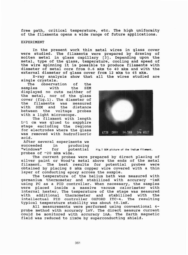
free path, critical temperature, etc. The high uniformity of the filaments opens a wide range of future applications.
EXPERIMENT
In the present work thin metal wires in glass cover were studied. The filaments were prepared by drawing of molten metal in glass capillary [ 3 ] . Depending upon the metal, type of the glass, temperature, cooling and speed of the wire spinning it is possible to produce filaments with diameter of metal core from 0.6 m)an to 40 mkm and with the external diameter of glass cover from 12 mkm to 45 mkm.
X-ray analysis show that all the wires studied are single crystals.
The observation of the samples with the SEM displayed no cuts neither of the metal, nor of the glass cover (fig.1). The diameter of the filaments was measured with SEM and the distance between the voltage probes with a light microscope.
The filament with length l2-1 cm was glued to sapphire stage excluding the regions for electrodes where the glass was removed with hudrofluoric acid. After several experiments we succeeded in producing "windowsn for potential ~ i g . 1 sEn picture of the i n d i u filament. probes of -20 mkm wide.
The current probes were prepared by direct placing of silver paint or Wood's metal above the ends of the metal filament. The best results for potential probes were obtained by placing 8 mkm copper wire covered with a thin layer of conducting epoxy across the sample.
The temperature of the helium bath was measured with germanium thermometer and stabilized with accuracy -1mK using PC as a PID controller. When necessary, the samples were placed inside a massive vacuum calorimeter with internal heater. The temperature of the stage was measured with additional thermometer and stabilized with the intellectual PID controller OXFORD ITC-4. The resulting typical temperature stability was about +O.lmK.
All measurements were performed using conventional 4- probe method with accuracy InV. The direct measure current could be monitored with accuracy 1nA. The Earth magnetic field was reduced to SlmOe by superconducting shield.
THEORY
Soon after the experimentalobservationof a step-likeV(I) structure of tin whiskers [1] several theoreticalmodels were derived to describethe observedphenomena.Oneline of development [4-6] introducedthe phenomenologicalconception of the PSC activation.Another line of work,culminatingin the work [7], has been to explore the timedependent Ginzburg-Landau (TDGL) equations, andnonequilibriumextensions thereof. And the third line oftheoretical investigations was summarized in [8],emphasizingthe static solutionsof equations taking fullaccount of nonlinear effects of large supercurrentdensities.
The phenomenological models [4-6] associates thevoltage steps with activation of PSC along the one-dimensionalsuperconductor.The PSC is a region of weakenedsuperconductivity(the S-S'-S boundary)with the region S'of the weak core _(T). If the voltage V across the PSC isnon-zero the phase 2_,(t_,_,ofthe superconductingorderparameter T(r,t)= T _----_I increases as a function oftime: d_/dt=2eV/h This leads to an increaseof v_0(r,t)andthus increaseof "thesupercurrentjs~ITlZv_.However, withincreasing Js the absolute value of the order parameter
z will decrease,wTh_ critical value Jc will be reachedas soon as IT12=2/31--oi, correspondingto v_(T)=i/_3, andthe superconductorwill enter the normalconductingstate.
The idea of PSC is related with the assumption thatthe phase _(r,t) is periodically reduced by 2E tocompensate the monotonic growth of the time-dependentphase. In order to explain the co-existence ofsuperconductivityand non-zero voltage along the one-dimensionalsample in a wide range of transport currentsI>Ic within the phenomenologicalmodels [4-6], one shouldinvolve the model of a two-fluid superconductivity.Thesuperconducting and the normal current components areassociated with non-stationary concentrations of Cooperpairs and quasiparticles.A few moments after the phase-slip event the normal current componentIn will carry themost part of a total current I=_+Is: vi0=0in the PSC coreand thus the supercurrentjs~l_Jz_ is close to zero. Whilejust before the phase-slipevent the supercurrentwill beclose to its criticalvalue Ic. In order the above processcould be stationaryin time the periodic variation of thephase _(r,t) by 2= should compensatethe monotonic growthof the phase duringone period_slip:
362
_lip
2_--_(O)-_(_slip) = 2e/hlV(t)dt=2e/h<V>_sli p (2),
0
where <V> is the time-averaged voltage across the PSC. Thisleads to the well known Josephson relation:_sliD=2_/_sliD=2e<V>/h.
_Skocpol,_Beasley and Tinkham (SBT) [5] postulated thatthe phase-slip event occurs within the range N_(T) of thePSC core, while the non-equilibrium quasipart_%es chargeimbalance relax on a length scale A=(I/31VF_in) /_, where 1is the mean free path, VF- the Fermi velocity and _in isthe inelastic relaxation time for normal particles. Thedifferential resistance (dV/dI)i is associated with theresistance of the normal-like section of length L(i)=2A.
Later Kadin, Smith and Scocpol (KSS) developed adetailed model of a charge imbalance wave equation for aPSC connected to a transmission line [6]. The KSS modelincludes the SBT [5] as a limit of a diffusive decay of acharge imbalance. However, KSS showed that under someconditions the relaxation of charge imbalance may resultsin propagating of charge-imbalance waves on the scales muchgreater than the A of SBT model. Therefore, the KSS modelpredicts the long-distance interaction of the PSC.
The above simplified review of the phenomenologicalmodels [4-6] outlines the main features of the PSCconception. Theoretically more strict developments [7,8]includes the phase-slip solutions as a limit.
Introducing the TDGL equations Kramer and Baratoff [9]obtained the following results:
I) When the current I is less than some value I1 thesuperconductor enters a uniform current-carrying state.
2) When the current I is larger than the threshold value12 the superconducting current-carrying state transformsinto an expanding domain of normal phase. The thresholdcurrent 12 coincides with the stability limit of thenormal-superconducting interface studied by Likharev [I0].
3) In the interval between I1 and 12 there exist asolution which corresponds to phase slippage. The one-dimensional sample remains superconducting over the itslength, but a_ some point local oscillations of the orderparameter I_Iz take place. When I_Iz turns to zero thephase _ experiences a jump of 2_.
The numerical solutions of the TDGL equat_ [Ii, 12lgive for a PSC region size of the order N_(T)F / , whereofis the pair-breaking term: F=(8F5.79_inTc)(I-T/Tc)-_i_'Thus the TDGL equations predict the long-range interaction.The distance of this interaction diverges rapidly at Tc.
363
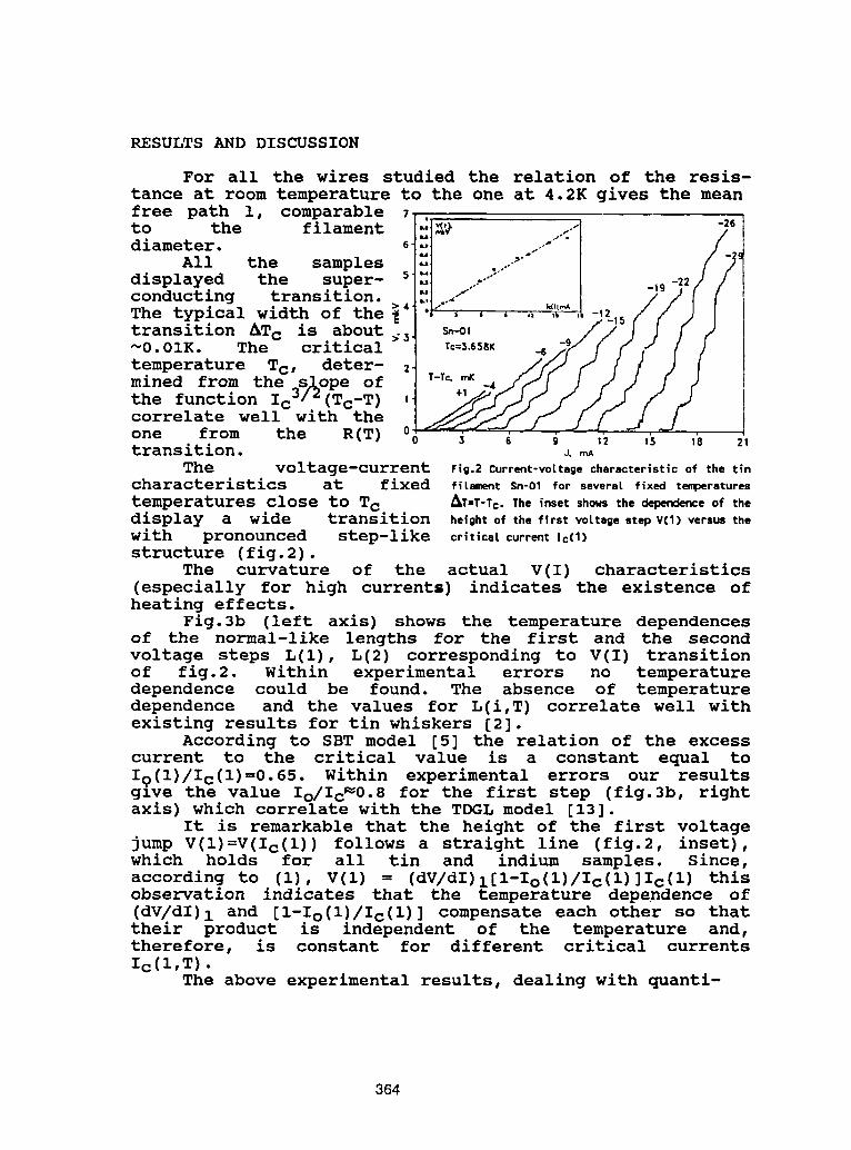
RESULTS AND DISCUSSION
For all the wires studied the relation of the resis-tance at room temperature to the one at 4.2K gives the meanfree path I, comparable 7to the filament _'_ -2,diameter. 6
All the samples _o...displayed the super- 5 ..ooconducting transition. .._/°° -,9The typical width of the _4 -,2transition _Tc is about _--0.OIK. The criticaltemperature Tc, deter- 2mined from the slope ofthe function Ic3/2(Tc-T) , +'correlate well with theone from the R(T) 0transition. 0 _ 8 9 12 ,s 18 zlJ,mA
The voltage-current Fig.2 Curr_t-vottage char_teristic of the tincharacteristics at fixed first sn-01forseveratfix_ temperaturestemperatures close to Tc _T"T-Tc.Thei_etsho_thed_e ofthedisplay a wide transition heightofthefirstvottagest_ V(1)vers_thewith pronounced step-like criticatcurr_tIc(1)structure (fig.2).
The curvature of the actual V(I) characteristics(especially for high currents) indicates the existence ofheating effects.
Fig.3b (left axis) shows the temperature dependencesof the normal-like lengths for the first and the secondvoltage steps L(1), L(2) corresponding to V(I) transitionof fig.2. Within experimental errors no temperaturedependence could be found. The absence of temperaturedependence and the values for L(i,T) correlate well withexisting results for tin whiskers [2].
According to SBT model [5] the relation of the excesscurrent to the critical value is a constant equal toI9(I)/Ic(I)=0.65. Within experimental errors our resultsglve the value Io/Ic_0.8 for the first step (fig.3b, rightaxis) which correlate with the TDGL model [13].
It is remarkable that the height of the first voltagejump V(1)=V(Ic(1)) follows a straight line (fig.2, inset),which holds for all tin and indium samples. Since,according to (i), V(1) = (dV/dI)l[l-Io(1)/Ic(1)]Ic(l)thisobservation indicates that the temperature dependence of(dV/dI)l and [1-Io(1)/Ic(1)] compensate each other so thattheir product is independent of the temperature and,therefore, is constant for different critical currentsIc(l,T).
The above experimental results, dealing with quanti-
364
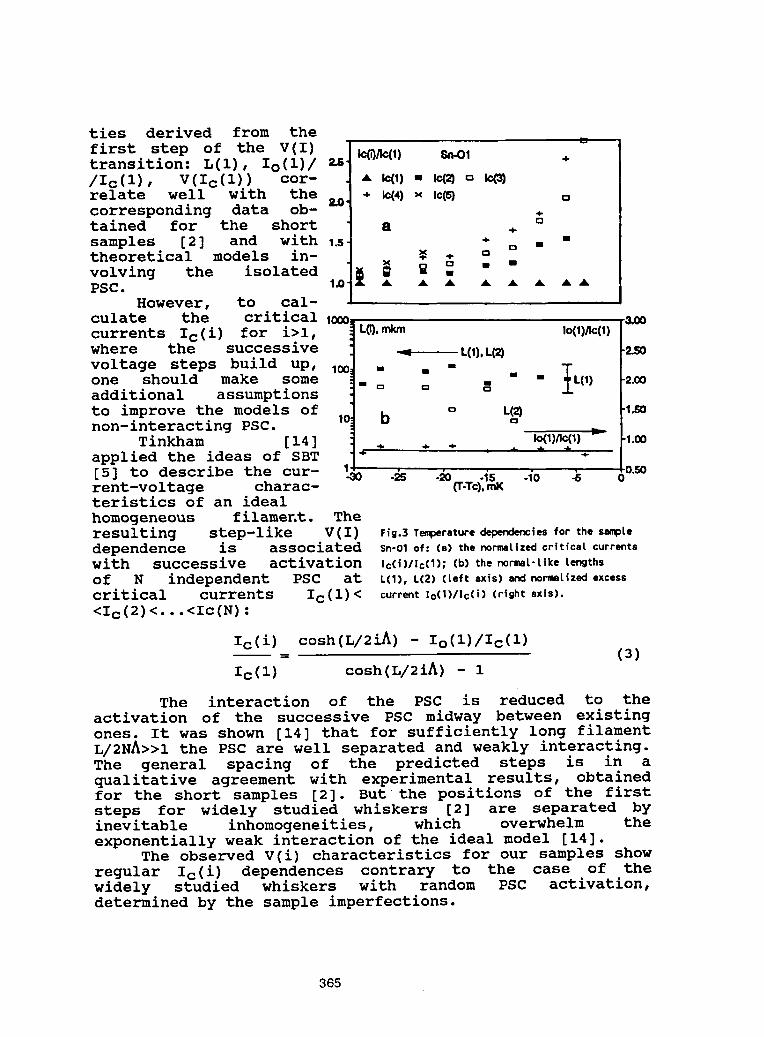
ties derived from the
first step of the V(I) I_4i)/Ic(I) 8n-01transition: L(1), io(1)/ 2.5, ./Ic(1), V(Ic(1)) cor- A _I) - _ o _4relate well with the 2.0, . _4) × I¢_ ocorresponding data ob- .otained for the short 8 .samples [2] and with . "o mtheoretical models in- _ . o
o m wvolving the isolated _ _ .PSC. I_ A A A A A A AHowever, to cal-
culate the critical I000 -&_currents Ic(i) for i>l, L_.mkm I_I)_(I)where the successive _ L(1),L_ -Z_voltage steps build up, I_ - . " Tone should make some " " _L(D 2._additional assumptions " _ o
to improve the models of 10 b o L(_o -I._non-interacting PSC.
Tinkham [14] . . . _I)_(I) -I._applied the ideas of SBT . : .
[5] to describe the cur- _ ._ "_.Tc-_s_mK-10 • 00"_rent-voltage charac-teristics of an idealhomogeneous filament. Theresulting step-like V(I) Fig.3T_ratured_x_i_ forthesampLedependence is associated sn-01of:(a)the_LJz_ ¢r|ticaLcurr_tswith successive activation [c(i)l]c(1);(b)the_m_L-LJkeLengthsof N independent PSC at L(1),L(2)(Leftaxis)a__Liz_ excesscritical currents Ic(i)< curr_t[0(1)llc(i)(rishtaxis).<Ic(2)<...<IC(N):
Ic(i) cosh(L/2iA) - Io(1)/Ic(1)-- = (3)IC(I) cosh(L/2iA) - 1
The interaction of the PSC is reduced to theactivation of the successive PSC midway between existingones. It was shown [14] that for sufficiently long filamentL/2NA>>I the PSC are well separated and weakly interacting.The general spacing of the predicted steps is in aqualitative agreement with experimental results, obtainedfor the short samples [2]. But the positions of the firststeps for widely studied whiskers [2] are separated byinevitable inhomogeneities, which overwhelm theexponentially weak interaction of the ideal model [14].
The observed V(i) characteristics for our samples showregular Ic(i) dependences contrary to the case of thewidely studied whiskers with random PSC activation,determined by the sample imperfections.
365
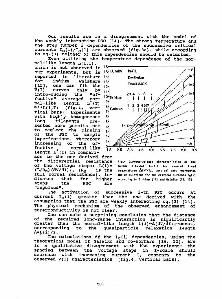
Our results are in a disagreement with the model ofthe weakly interacting PSC [14]. The strong temperature andthe step number i dependencies of the successive criticalcurrents Ic(i)/Ic(1) are observed (fig.3a). While accordingto eq.(3) neither of this dependencies should be detected.
Even utilizing the temperature dependence of the nor-mal-like length L(1,T),which is not observed in 16- i=9our experiments, but is 15-U,mkV In-FIh /"./
reported in literature 14- D=6mkm i_i.,...._e
for indium whiskers 13- Tc=3.340K i I°'.'"i=7[15], one can fit the 12- //°/
o- ..o f .V (I) curves only by 1I- 234 5 6 7 .,"_ ,.'/"I.....i=6
intro-ducing the "ef- 10_nkh_nIIJJ l J ] "°9"/_"./'/"/""":"/ l /_/fective" averaged nor-mal-like length L*(T) 9- ..,;Y!'_o"_,./°......i=5_8*L(I,T) (fig.4, ver- 8- . I 2 3 4567/_./o,.,.,/_/_""'°Ii0-.°.°fGala,ko I I I I l,l'f2".._" .......1 _,_,,tical bars). Experiments 7" ."."I..'"l".('-"./'" _I'''='_/°/ 2" t._"./" _.--f
with highly homogeneous 6- /.,..,.:.,.o//:o.:_":j...11"/I/'/'::5-/-./_//°_/.-i=3"long filaments pre- 5- T-To=__.__- :sented here permits one 4- i":::_";-_'._...--'"f /i=2
to neglect the pinning 3- .._>::5;..--._,--_ -_!_ _5_/__of the PSC to sample 2- _."!_i_.-___ _i=l-:-imperfections. Thereforeincreasing of the ef- I- .,,'_i_.-':_ _ J__L-_--_ ,--̂
I_..-::....._._._ .-----_ I,mAfective normal-like .5 2.5 3.5 4.5 5.5 6.5 7.5 8.5 9.5length L*(T) in compari-son to the one derived fromthe differential resistance Fi..4 Current-voltagecharacteristicsof theof the voltage steps: L(i)= indiumfitment In-Fitfor severerfixed(L/Rn)(dV/dI)i, (Rn - is the t_peraturesAT=T-To.Vertica[barsrepresentsfull normal resistance), in- thecatcutati_f0rthe¢ritlcatturretsIt(1)dicates that for higher _cordingtoTinkham[14]andGa[siko[16,IZ].steps the PSC are"repulsed".
The activation of successive i-th PSC occurs atcurrent Ic(i) greater than the one derived with theassumption that the PSC are weakly interacting eq. (3) [14].The physical mechanism of the observed enhancement ofsuperconductivity is not clear.
One can make a surprising conclusion that the distanceof the required long-range interaction is significantlygreater than the normal-like length L(i)--A(dV/dI)i--const,corresponding to the quasiparticle relaxation lengthA=L(i)/2.
The calculations of the Ic(i) dependencies, using thetheoretical model of Galaiko and co-workers [16, 12], arein a qualitative disagreement with the experiment: thespacing between the voltage steps in I-scale shoulddecrease with increasing current I, contrary to theobserved V(I) characteristics (fig.4, vertical bars).
366
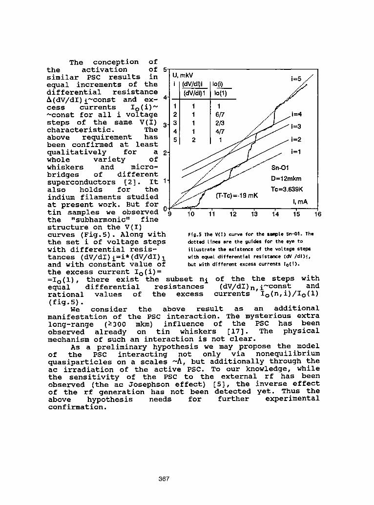
The conception ofthe activation of 5
similar PSC results in U,mkV i=5.o../equal increments of the i (d_dl)i Io(i)differential resistance (dV/dl)1Io(I)_(dV/dI)i-const and ex- 4cess currents Io(i)_ I I I_const for all i voltage 2 I 6_ i=4
steps of the same V(I) 3 3 I 2_ i=3characteristic. The 4 I 4_ "°"above requirement has 5 2 I i=2been confirmed at leastqualitatively for a 2 i=Iwhole variety ofwhiskers and micro- /0" Sn4D1bridges of differentsuperconductors [2]. It I D=12mkmalso holds for the Tc=3.639Kindium filaments studied _-Tc)=-19mKat present work. But for l,mAtin samples we observed 09 10 11 12 13 14 15 16the "subharmonic" finestructure on the V(I)curves (Fig.5) . Along with Fig.5TheV(1)curveforthesampteSn-01.Thethe set i of voltage steps _tt_ ti_s,retheSuitsfortheeyetowith differential resis- itt_tratetheexistenceof thevottagestepstances (dV/dI)i=i*(dV/dI)1 with_t differ_tla|resist,_e(_ /dl)i,and with constant value of _twithdiffer_t excesscurr_tsIo(1).the excess current Io(i)==Io(1), there exist the subset ni of the the steps withequal differential resistances (dV/dI)n,iNconst andrational values of the excess currents Io(n,i)/Io(1)(fig.5).
We consider the above result as an additionalmanifestation of the PSC interaction. The mysterious extralong-range (a300 mkm) influence of the PSC has beenobserved already on tin whiskers [17]. The physicalmechanism of such an interaction is not clear.
As a preliminary hypothesis we may propose the modelof the PSC interacting not only via nonequilibriumquasiparticles on a scales -A, but additionally through theac irradiation of the active PSC. To our knowledge, whilethe sensitivity of the PSC to the external rf has beenobserved (the ac Josephson effect) [5], the inverse effectof the rf generation has not been detected yet. Thus theabove hypothesis needs for further experimentalconfirmation.
367
SUMMARY
The step-like current-voltage characteristics ofhighly homogeneous single-crystalline tin and indium thinfilaments has been measured. The length of the samplesL_icm was much greater than the nonequilibrium quasipartclerelaxation length A.
The quality of the filaments gives the possibility toneglect the pinning of the PSC to the sample imperfec-tions. This assumption is confirmed by the reproducibilityof the results for the samples cut from different parts ofthe same wire and by the observation of definite dependenceof the critical currents Ic(i) versus the step number i.
Quantitative values, obtained from the first voltagesteps of the V(I) curves (the activation of the solitaryPSC) agree with the experiments reported previously forwhiskers and microbridges [2] and correlate withcorresponding calculations [5, 12, 15].
The observed enhancement of superconductivity forhigher voltage steps and the "subharmonic" fine structurecould not be understood within the existing theories ofweakly interacting PSC.
ACKNOWLEDGEMENTS
The authorsacknowledgeProf. Yu.P.Gaidukov,Dr.Ya.G.Ponomarevand Dr. M.Yu.Kupriyanovfor valuablediscussions.
REFERENCES
[1] J.D.Meyer, App[.Phys. _, 303, (1973)[2] R.Tideck$, "Current Induced NoneclUitibrium Pher_nene |n Quasi-One-Dimenstorust
Superconductors., (Springer, 1990)
[3] H.B.Brandt, O.B.Gitzu, A.H.Josher, B.P. Kotrubenko and A.A.Hikotaeva, Soy.: "Pribory 1Technika Experiments" n.3, 256, (1976)
[4] T.J.Riger, D.J.Scatapino and J.E.Hercerau, Phys.Rev.B, 6, 1734, (1972)
[5] W.J.Scocpo|, M.R.Beastey and H.Tinkham, J.Low Tesnp.Phys.16,145, (1974)[6] A.H.Kedin, L.lt.Smith and W.J.Scocpot, J.Low Temp.Phys.38, 497, (1980)
[7] L.Krmer and R.Watts-Tobin, Phys.Rev.Lett., 60, 1041, (1978)[8] V.P.Gatiliko, J.Lo_ Temp.Phys., 26, 683, (1977)
[9] L.Kramer and A.Saratoff, Phys.Rev.Lett, 38, 518, (1977)[10] K.K.L|kharev, Sov: Pis,ima v Zh.Eksp.i Teor. Fiz, 20, 730 (1974)
[11] B.%.Iviev, N.B.Kopnin and L.A.Hastova, Zh.Eksp.i Teor. Ffz, 78, 1963, (1980)[12] V.P.Ga|aiko and N.a.Kopnin, .Nonequitibrium Superconductivity", Etsevier Sc|. Pub|., 1986
[13] L.Krmer and R.Range|, J.Lo_ Temp.Phys.57, 391, (1984)[l&] N.Tinkham, J.Low Temp.Phys., 35, 147, (1979).
[15] R.Tidecks, G.Stama, Z. Physik B, 37, 103, (1980)[16] E.V.Bez_ty, E.tl.Brstus and V.P.Gataiko, Soy: Fizikl Wizkih Teqoeatur, _, 1010, (1977)
[1TJ R.Tidecks, J. Low Temp. Phys, 58, 183, (1985)
368

THIS PAGE INTENTIONALLY LEFT BLANK


Fabrication Methodology
Chair: Dr. U. Balachandran
HIGH Tc SUPERCONDUCTORS FABRICATED BY PLASMA AEROSOL MISTDEPOSITION TECHNIQUE
X. W. Wang, K. D. Vuong, A. Leone, C. Q. Shen, J. Williams, and M. CoyAlfred University, Alfred NY
ABSTRACTWe report new results on high % superconductors fabricatedby a plasma aerosol
mist deposition technique, in atmospheric environment.Materials fabricated are YBaCuO,BiPbSrCaCuO, BaCaCuO precursor films for TIBaCaCuO, and other buffers such asYSZ. Depending on processing conditions, sizes of crystallites and/or particles arebetween dozens of nano-meters and several micrometers. Superconductive properties andother materialcharacteristics can also be tailored.
I. INTRODUCTIONSince the discoveriesof highTosuperconductorsbetween 1986 and 1993, different
film fabrication techniques have been developed [1-3]. These techniques can be classifiedas thin film and thick film processes. The thin film processes include electron-beamevaporation, sputtering, and laser ablation [2,4-5]. The thick film processes include inkprinting,tape casting, and plasma powder spray [6-8]. In the thin film processes, materialsdeposited onto the substrates can have atomic, ionic, or molecular sizes. Resulting thinfilms usually have high qualities and high densities. However, film growth rates in thinfilm processes are relatively slow, which could not be applied in large scale productions.As far as thick film processes are concerned, materials' sizes are 1-10 micrometers, filmgrowth rates are relatively fast, but resulting filmsare usually inhomogeneous and porous.To find compromises between thin and thick film processes, other fabrication techniqueshave been developed such as pyrolysis chemical vapor deposition, mist deposition inmicrowave chambers [9], RF plasma mist deposition in enclosed chambers [10], and RFplasma mist deposition in atmosphericenvironment [11]. In this paper, we shall reportnew results obtained via the last process. Operational principlesare briefly explained insection II, materialsdeposited are presented in section III, plasma-experimentalconditionsare given in section IV, results are summarized in section V, and future work is discussedin section VI.
H. OPERATIONALPRINCIPLEIn this RF plasmaaerosoldepositionprocess, an aerosolmist containingdesired
cationsis injectedinto a plasmaregionwherethe maximumtemperatureis 10,000K andthe gas pressureis slightlyhigherthan one atmosphere. Attervaporizationand collision,ions or groups of ions with sufficientmomentatravel towards a collectoroutside theplasmaregion. Dependingon temperatureprofilesof the collector,nano-sizedparticles,particleclusters,or micro-sizeddepositscan be formed. In Figure 1, an experimentalsetup is illustrated,where the collector is a substratewith its heater block. Besides thesubstrateassembly,there aretwo otherassemblies:startingmaterialassemblyandplasma
372
reactor assembly. The starting material assembly consists of an ultrasonic nebulizer, asolution container, a carrier gas inlet, and a mist outlet. The plasma reactor assemblyconsists of an RF coil with two copper leads (power suppliedby an RF generator, 4 MHz,35 kW), a plasma gas nozzle device with three plasma gas inlets, a quartz tube, a mistinlet, and a flame outlet. To prepare a solution, nitrates and/or chlorides with desiredcations are dissolved in distilledwater. The aqueous solution is poured into the solutioncontainer. When the ultrasonic nebulizer vibrates at a frequency of 1.63 MHz, thesolution is excited into aerosol mist with droplet sizes of 5 - 10 micrometers. Under thepressure of a carrier gas (Ar), the mist is fed into the plasma reactor. After vaporizationand deposition, films and/or materials are formed on the substrate (collector).
Around the middle section of the quartz tube, ion sizes are estimated to be 1 - 3angstroms. Near the exit end of the tube (flame outlet), sizes of travelling particles areestimated to be 5 - 10 nanometers [12]. Particle clustering is expected to take place in theflame region, and nucleation is expected on the substrate. Besides substrate temperature,filmmorphology and grain sizes maybe affectedby the distance between the substrate andthe flame outlet, plasma power coupled to the RF coil, plasma gas feeding rates, mistingrates, and solution concentration. Oxidation process may be initiated in the quartz tube,enhanced by auxiliary oxygen supply near the flame outlet (not shown), and near thesubstrate.
HI. MATERIALS DEPOSITEDA. BiSrCaCuO systems
In an earlier experiment, films with 2212 composition were fabricated with theplasma technique [13]. Recently, a group at SUNY Buffalo found that the 2223fabrication window was approximately 5°C [10]. To ease fabrication conditions for largescale productions of 2223 film coatings, a bulk processing technique called two-powderprocess provided an alternate route [14]. In this bulk process, 2212 was first formed,0011 was then added to form 2223.
In this work, we attemp to fabricate Bi2.2.xPbxSr2.yCal+yCu208(2212) films; withx=0.20, 0.25, 0.30; and y = 0.25, 0.50, 0.75; as illustrated in Table I. Once 2212 film isformed, 0011 can then be added.
B. YBaCuO systemsFilms of superconductive 123 phase were deposited at a substrate temperature of
approximately 600°C, without post-annealing [11]. For a film deposited on MgO singlecrystal, superconductive transition temperature was 100 K, zero resistance temperaturewas 93 K, with transition width (10-90%) of 3 K [15]. It was observed that sizes ofdeposited oxides could be as smallas 20 nanometers [16].
In this work, we attempt to fabricate nano-sized 211 powder. It is known that 211affects the superconductivity of 123 phase. For example, the critical current (Jc) of 123superconductor can be altered by the presence of211 phase [17-18]. When Jcis enhanced,211 particles are assumed to be flux pinningcenters. WhenJc is reduced, 211 particles are
373
assumed to be a micro-sized impurities blocking supercurrent flow. To clearlyunderstand the roles played by the 211 phase, nano-sized particles are needed. Once theseparticles are produced with uniform particle size distributions, we can carry out wellcontrolled doping experiments to systematically study pinning effects, kinetics, andmechanicalproperties.
C. BaCaCuO precursor films for TIBaCaCuO systemsIn an earlier experiment, 0223 precursor films were deposited by the plasma
technique. The precursor filmswere annealed at different substrate temperatures in a one-zone furnace to form 2212 and 2223 phases [19]. Recently, it was observed that 1223phase has better critical current properties under high magneticfield than that of 2212 and2223 phases. To fabricate a 1223 film,DeLuca developed a two-zone furnace technique[20].
In this work, we attempt to fabricate 0223 precursor filmswith different porositiesand different dopants. When the porosity of a film can be tailored, we shall be able tocontrol Tl diffusion processes in a two-zone furnace. When a metallicoxide such as silveroxide can be doped, we shallbe able to align 1223grains to enhance Jc.
D. Other buffer or hybrid materialsIt has been a great challenge to coat YBaCuO on nickel containing substrates. If a
buffer layer can be inserted between the substrate material and the superconductivematerial, this buffer layer can stop interdiffusion, can match lattice parameters, and canmatch thermal expansion coefficients. In this work, we attempt to deposit yttria stabilizedzirconia, tin oxide, and silicon oxide. With superconductors, the last two coating layerscan also be utilized as optical couplers and other hybrid optoelectronic films.
IV. PLASMA EXPERIMENTAL CONDITIONSDuring plasma experiments,all parameters were optimized, as listed in Table II. In
BiPbSrCaCuO experiments, nine batches of solutions were prepared according to thestoichiometric ratios listedin Table I. Each batch of films was deposited at two different
substrate temperatures ranges. The low temperature range was from 400-600°C, whilethe high temperature range was 600-750°C. The films deposited at low substrate
temperatures were heat treated in a furnace at 800°C for one hour to enhance 2212 phaseformation. For comparative purposes, bulk powders were used to fabricate thesuperconducting phases represented by equations 1-9 [21]. These samples were preparedby a solid state reaction method. That is, powders of CaCO3, CuO, SrCO3, Bi203, andPbO were mixed in the ratios listed in Table I. These mixtures were then calcined andannealed in an atmosphericallycontrolledfurnace several times to form 2212 phases.
To prepare solutions for Y2BaCuOs,the stoichiometric ratios of Y:Ba:Cu rangedfrom (0.161):(0.158):(0.158)to (0.194): (0.171) : (0.172). During fabrication of 211materials, the collector (substrate) temperature was maintained at a temperature of 400 to660oc.
374
To prepare solutions for BaCaCuO (0223), the mole ratio of Ba:Ca:Cu was0.16:0.13:0.18 mole, with additional 0.01-0.02 mole of Ag in some experiments. Thesubstrate temperatures ranged from 500 to 750°C.
To prepare yttria stabilized zirconia, zirconyl nitrate and yttrium nitrate powders(10 mol%yttrium) were mixed in the appropriate ratio and dissolved in distilled water.
The substrate temperatures ranged from 600-950°C.
To prepare solution for tin oxide, SnCI4"5H20,HCI, and distilled water weremixed to produce solution with a concentration of 100 g/l. To prepare silica solution, astarting suspension containing silicon oxide powder (7 nm) and water was mixed toproduce solution with a concentrations of 10 to 40 g/l.
V. RESULTS AND DISCUSSIONAll films and materials were characterized by x-ray diffraction (XRD), energy
dispersive spectroscopy (EDS), and scanningelectron microscopy (SEM). Resistances ofsome filmswere measured by a four-point lead method, as a function of temperature.
1. BiPbSrCaCuO FilmsFrom EDS measurements,all cations (metals) were observed in the BiPbSrCaCuO
films. From SEM analysis, filmthickness, morphology, and microstructures were studied.Filmthicknesses were between 3 and 12 micrometers. As-deposited filmscontained plate-like crystals, with crystal sizes of 1-5 micrometers. However, crystal shapes weredependent on the cation ratios. Referring to Table I, crystals of equations 2-4, and 7-8had more edges, indicatinga more dendrite growth.
As verified by XRD measurements, when films were deposited at low substrate
temperatures (<600°C), 2201 phase was the dominant phase along with 2212 and otherbinary and ternary phases as minor phases. After post-annealing at 800°C for one hour,2212 phase was enhanced. However, when films were deposited at high substrate
temperatures (>600°C), 2212 phase was the dominant phase in each as-deposited film asillustrated in Table I and Figure 2 (corresponding to Eqn. 7) [22]. There was also anindication of preferred 001orientation, which indicated a possibilityof liquid phase growthfrom small deposits in the ranges of 50 to 150 nanometers as determined from the FullWidth Half Maximum(FWHM) of an XRD pattern by a program called SHADOW.
In comparison, a series of bulk processing experiments were conducted with nineidentical equations listed in Table I. It took several thermal cycles to fabricate 2212 bulkmaterials. However, with this plasma technique, 2212 materials were synthesized withinone deposition process.
2. Y2BaCuO_(211)Y2BaCuO5powders were scrapped off a flat MgO collector (5cm x 5cm). XR
measurements revealed that powders were phase pure 211 when the starting materialratios were from (0.190):(0.158):(0.158)to (0.194):(0.158):(0.157)for Y:Ba:Cu, as
375
illustrated in Figure 3. As the ratios were outside of the range, other non-211 phases werepresented as minor phases, as illustrated in Table III. The crystallite size increased from53 to 116 nm when collector temperature increased from 500°C to 660°C. Initial SEManalysis of as-deposited powders revealed that these powders were agglomerated.Powders were then dispersed in acetone (containing Darvan 821 deflocculant), andvibrated in an ultrasonic oscillator. Particle sizes of those powders were approximately100-300 nm, as estimated by SEM measurements.
3. BaCaCuO Precursor (0223)For a precursor film, XRD reveals that barium copper oxide and calcium copper
oxide phases were present. With silver dopant, silver metal was present from XRDpattern. The crystallite sizes ranged from 70-150 nm (from SHADOW). EDS results
verified the existence of all desired cations. For the film deposited at 450°C, the particlesizes were relatively uniform (0.5-1.5 micrometers) and the film was porous. The filmdeposited at 650°C had particle sizes ranged from 0.5 to 10 micrometers and the film wasdense. After thallination in a two-zone furnace, XRD revealed that the films were 1223phase pure, and four-point-probe measurements revealed that zero resistance temperaturewas 108 K [23].
4. YSZ
Thin films of YSZ were deposited on Ni containing substrates. All as-depositedfilmswere yttria stabilizedcubic zirconia as determined by XRD. The deposition rate wasdependent on the feed flow rate, reactor-substrate distance, nebulizer setting, and solutionconcentration. The film thicknesses ranged from 5 to 30 micrometers depending on theduration of deposition and other experimentalconditions as those listed in Table I. Thedensity and morphology of the film were dependent on the substrate temperature anddeposition rate. It was observed that films deposited below 900°C have "snowflakes"appearance with low density and poor adhesion. When the substrate temperature washigher than 900°C, the film density and adhesion strength were increased. Post heattreatment slightly enhanced the density and adhesive strength of these films. Surfacemorphologies of the as-deposited and post heat-treated filmswere different. In general,the post-annealed filmswere more crystallized than the as-deposited films.
6. Tin Oxideand SilicaIntin oxidefilms,XRDrevealedthat the predominantphasewas SnO2(Cassiterite
- JCPDScard # 41-1445). Mossbauerspectrometrydeterminedthat the tin was in its +4oxidationstate. The crystallitesize was determinedto be -25 nm via XP,D SHADOWprogram. SEM analysisof the films showed a particle size ranged from 0.4 to 4micrometers. In addition,siliconoxide filmswere depositedon SLS glass substrates.When the solutionconcentrationincreasedfrom 10-20g/lto 40g/l, films changedfromamorphousto crystallinestructuresas verifiedbyXRDand SEM.
376
VI. DISCUSSIONPlasma aerosol deposition techniquehas potentialfor large scale coatings such as
underground superconductorcables and magnetic shieldings. To fully develop thetechniqueinto a matureprocess,we arecurrentlyconductingthe followingexperiments:1. to add(BiSrCaCuO)0011 into2212 to form2223;2. to dope nano-sized211 powder into 123 superconductorand to comparethe resultswith that obtained from the micro-size powder;3. to hybridize123with others magneticmaterials;4. to improve the 0223 precursor film's properties by changing the experimentalparameters,andto studythe rolesplayedby silver.
Acknowledgment
We wouldliketo thankDr. R.L. Snyder,Dr. S.Dorris,Dr.K. Gorreta,Mr.RobertKampwirth,Mr. T. Hardy,Dr. C. Oberly,Dr. R.M.Spriggs,andDr. L.D.Pyefortheirhelp. Part ofthe workwas initiatedatArgonneNationalLaboratorywhenDr. X.W.Wangwas a summerfacultyofDOEEducationDepartment.Thisworkwas partiallysupportedbyArgonneNationalLaboratory,U.S. AirForce,Centerfor AdvancedCeramicTechnology,andNSFIndustryCenterfor GlassResearch.
ILF,EF,gP22C,F,S
1. J. Talvacchio et al, "YBCO and LSCO Films Grown by Off-Axis Sputtering," inScience and Technology of Thin Film Superconductors 2; Ed. by R.D. McConnell and R.Noufi, Plenum Press, New York, 1990.2. M. G. Krishna et al, "Single Source Electron Beam Evaporation of Bi-Sr-Ca-Cu-OThin Films," in Science and Technology of Thin Film Superconductors 2, Ed. by R.D.McConnell and R. Noufi, PlenumPress, New York, 1990.3. D. H. Kuo et al, "Preparation of Superconducting TI-Ba-Ca-Cu-OFilms by Diffusion
Method," in Science and Technology of Thin Film Superconductors 2_ Ed. by R.D.McConnell and R. Noufi, PlenumPress, New York, 1990.4. N. G. Dhere et al, "Control of Thickness and Composition Uniformity in SputteredSuperconducting Thin Films," in Science and Teehnolo_, of Thin Film Superconductors2, Ed. by R.D. McConnell and R. Noufi, PlenumPress, New York, 1990.5. T. Frey et al, "In-Situ Deposited Superconducting Laser Ablated Thin Films of
YiBa.zCu307.x and Bi0.sPb0.2Sr0.gCalCul.6Ox,"in Science and Technology of Thin FilmSuperconductors2, Ed. by R.D. McConnell and R. Noufi, Plenum Press, New York,1990.
6. U. Balachandran et al, "Sintering Bi2Sr2CaCu2OyPellets and Thick Films," inSuperconductivity and Ceramic Superconductors, Vol. 13, Ceramic Transaction, Ed. byK.M. Nair and E.A. Giess.
377
7. D. W. Johnson et al, "Processing and Jc Considerations in High-TemperatureSuperconductors," in Superconductivity and Ceramic Superconductors; Vol. 13, CeramicTransaction, Ed. by K.M. Nair and E.A. Giess.
8. T. Okada, H. Hamatani, and T. Yoshida, "Radio-Frequency Plasma Spraying ofCeramics," J. Am. Ceram. Sot., 72 [11] 2111-16 (1989).9. A. Koukitu et al, Jpn. J. of Appl. Phys. 28, L1212 (1989).10. A. Shah, S. Patel, E. Narumi, and D. T. Shaw, "In situ, rf plasma deposition ofBi2Sr2Ca.2Cu30x thin films at atmospheric pressure," Appl. Phys. Lett. 62 (19) 2422-24,1993.
11. X.W. Wang, H.H. Zhong, and R.L. Snyder,Appl. Phys. Lett. 57 (15) 1581 (1990).12. T. Yoshida, "The Future of Thermal Plasma Processing," in Materials Transactions,JIM, Vol. 31, No. 1 (1990), pp. 1-11.13. R.L. Snyder, X.W. Wang, and H.H. Zhong, U.S. Patent No. 5,120,703, June 1992.14. Process developed by S. Dorris and B.C. Prorok at Argonne. For detailedinformation, see, for example, B.C. Prorok, "Formation of the Bi2Sr2CazCu30xSuperconductor by a Two Powder Process," U. of Illinoisat Chicago, 1993.15. H.H. Zhong, X.W. Wang, J. Hao, and R.L. Snyder, "Deposition of SuperconductiveYBaCuO Films at Atmospheric Pressure by RF Plasma Aerosol Technique," inSuperconductivity and Its Applications_ Ed. by Y.H. Kao, A.I. Kaloyeros, and H.S.Kwok, AIP Conference Proceedings 251, Buffalo,NY 1991.16. J. Hao, X. W. Wang, and R. L. Snyder, "RF Plasma Aerosol Deposition ofSuperconductive YiBa.zCu3OT.x Films at Atmospheric Pressure," in Proceeding of theFourth National Thermal Spray Conference_Pittsburg, PA, 4-10 May 1991.17. Donglu Shi, S. Sengupta, and J.S. Luo, "Extremelyfine precipitates and flux pinningin melt-processed YBa2Cu3Ox," Physica C213 (1993) 179-184.18. S. Jin, T.H. Tiefel, and G.W. Kammlott, "Effect of Y2BaCuO5inclusions on fluxpinningin YBa2Cu307.x," Appl. Phys. Lett. 59 (5), 1991.
19. H.M. Duan, B. Dlugosch, A.M. Hermann, X.W. Wang, J. Hao, and R.L. Snyder,"Superconducting TIBaCaCuO Thin Films From BaCaCuO Precursors," inSuperconductivity and Its Applications, Ed. by Y.H. Kao, A.I. Kaloyeros, and H.S.Kwok, AIP Conference Proceedings 251, Buffalo, NY 1991.20. J.A. DeLuca, P.L. Karas, J.E. Tkaczyk, P.J. Bednarczyk, M.F. Garbauskas, C.L.Briant, and D.B. Sorensen, Physica C 205, 21 (1993).21. Unpublished results from X.W. Wang's experiments performed at Argonne NationalLab between May and June 1993.22. The crystallite size for 2212 film (eqn. 7) was -128 nm as determined fromSHADOW. Also the electrical resistance was measured by a four-point lead method. Foras-deposited films, superconductive transition temperature was 100 K for Equation 5 and90 K for Equation 2. The zero resistance temperature was 58 K and 60 K for Equation 5and Equation 2, respectively.23. Work performed by Mr. Robert Kampwirthat Argonne National Laboratory.
378
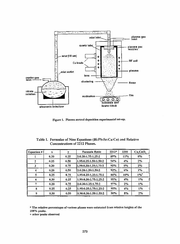
I
plasma gas
H '°'°'
mist (10 :lie
mistoutlet .... plasm
clustering_!,,_i_.........::...._ --flamenitrate_ -- _ -_.-..'/ [ ' ,",_--. 'solution I '_ _'-- • -A I ;"'"'" film
ultrasonicnebulizer heaterblock
Figure 1. Plasma aerosol deposition experimental set-up.
Table I. Formulae of Nine Equations (Bi:Pb:Sr:Ca:Cu) and RelativeConcentrations of 2212 Phases.
Equation # x y Formula Ratio 2212 _ 2201 C_CuO 3
1 0.20 0.25 2:0.20:1.75:1.25:2 89% 11% 0%
2 0.25 0.50 1.95:0.25:1.50:1.50:2 94% 4% 2%
3 0.30 0.75 1.90:0.30:1.25:1.75:2 93% 5% 2%
4 0.20 0.50 2:0.20:1.50:1.50:2 93% 6% 1%
5 0.25 0.75 1.95:0.25:1.25:1.75:2 86% 10% 1%+
6 0.30 0.25 1.90:0.30:1.75:1.25:2 95% 4% I%
7 0.20 0.75 2:0.20:1.25:1.75:2 97% 2% 1%
8 0.25 0.25 1.95:0.25:1.75:1.25:2 95% 4% 1%
9 0.30 0.50 1.90:0.30:1.50:1.50:2 90% 8% 2%
^ The relative percentages of various phases were estimated from relative heights of the100% peaks.+ other peaks observed
379
Table H. Film Deposition Conditions for Superconductingand Nonsuperconducting Materials.
Parameter Bi-2212 Y,BaCuOs Ba:Ca:Cu30, YSZ SnO: / Silica
PowerSetting 35 35 30 30 40%
Axial ArgonFlow 5 7 7 - 9 7 5Rate (L/min)
SwirlArgon Flow 10 7 - 10 8 - 10 10 7.5Rate(L/min)
Swirl/Tangential02Flow Rate 15 10- 15 15- 20 10 12.5
(L/min)
FeedArgon Flow 4 2.5- 4 3.5- 5 2.5 2.5Rate (L/min)
NebulizerSetting 80 80 75 80 50 / 100(%)
Substrate 13 12 13 12 11Distance(cm)
SubstrateTemp. 400- 750 400- 660 500 - 750 600 - 950 400 - 500('c)
SolutionCone. 100 120 100 75- 100 100/ 10-50(g/l)
Table HI. Solution Ratios and Substrate Temperatures Effectof Impurity and Crystallite Size.
Experimental Solution Mole Ratio Substrate Impurity Crystailite# (Y:Ba:Cu) Temp (°C) Size (nm)1 0.190 : 0.158 : 0.158 660 0 105
2 0.190 : 0.158 : 0.158 500 10% Y203 116
3 0.190 : 0.158 : 0.158 500 10% Y203 102
4 0.161 : 0.158 : 0.158 400 30% 123 66
5 0.190 : 0.171 : 0.172 530 15% 123 56
6 0.190 : 0.164 : 0.163 600 15% 123 80
7 0.190 : 0.159 : 0.157 550 10% 123 72
8 0.194 : 0.158 : 0.157 570 0 70
9 0.192 : 0.158 : 0.157 500 0 53
380
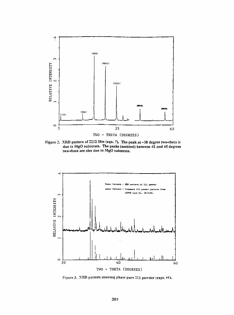
{008)
(oolo)
zr..T..1
_-4 _ (0012)r..T,.1;::::..I,-I
r=.l
(oo16)(oezl)
(006) ._
5 35 65
TWO - THETA (DEGREES)
Figure2. XRD pattern of 2212 film(eqn. 7).The peak at-38 degree two-theta isdue to MBO substrate. The peaks (omitted) between 42 and 45 degreestwo-theta are also due to NIgO suhstrate.
I, I, ,! I ,,_ _l I,,, ,,, ,1 L,1,11, !20 40 60
TWO - THETA (DEGREES)
Figure 3. XRD pattern showing phase pure 211 powder (expt. #1L
381
Partial Melting of Bulk Bi-2212
B. Heeb and L.J. Gauckler
Nichtmetallische Werkstoffe, ETH Ziirich, Sonneggstr. 5, CH-8092 Ziirich,Switzerland
Abstract
Dense and textured Bi-2212 bulksampleshave been producedby the partial meltingprocess. The appropriate amount of liquid phase necessary for complete densificationhas been adjustedby controlling the maximumprocessing temperature. The maximumtemperture itself has to be adaptedto several parametersas powderstoichiometry,silveraddition and oxygen partial pressure. Prolonged annealing at 850 and 820 °C andcooling in N2 atmosphere led to nearly single phase material with Tc=92 K. Criticalcurrent densitiesJc of 2'200 AJcm 2 at 77 K/0 T have been achievedin samples of morethan 1 mm thickness.Reducing the thicknessbelow 0.4 mm enhancesJc considerably tovalues > 4'000 A/cm2. The addition of 2 wt% Ag decreases the solidus temperature ofthe Bi-2212 powder by 21 °C. Therefore, the maximumheat treatment temperature ofAg containing samplescan be markedly loweredleading to a reductionof the amount ofsecondary phases. In addition, Ag enhances slightly the texture over the entire cross-section and as a result Jcat 77 K/0 T.
Introduction
Melt processingof Bi-2212 (Bi2Sr2CaCu20x) is a commonfabricationtechnologytoproducesuperconductingdeviceswith a dense,weak-linkfree microstructure.Variousgeometries have been producedby this technique:(a) Thick films on Ag-substratesarefabricatedby the so-called partial melting route [1,2] leading to an excellent grainalignment and high critical currentdensitiesat 77 and4.2 K even in long tapes. (b) Agsheathed wires are produced by a very similar process [3-5]. So far, good super-conductingpropertiesin long lenghts have been achievedat temperaturesbetween 4.2and 25 K. (c) Massivedevices,e.g. tubesandringsfor currentleadsand limiters, havebeen fabricated by complete melting at temperaturesabove 1000 °C. For thesegeometries, the high temperaturesare requiredto achieve the appropriateviscosity toform the desired shape [6], but they promoteoxygen loss during melting and thedevelopmentof an unfavorablemicrostructurewith coarse secondaryphaseseven afterprolongedannealingat temperaturesabove 800 °C [7-9]. As a consequence,the criticalcurrentdensity at 77 Kremains limited. Nevertheless, technical devices are feasiblewithbulk materialsdue tocomponentswith large cross-sectioncarryinghigh currents.
The purposeof this studyis to apply the partialmeltingprocess to producebulk Bi-2212 materialin orderto avoid the disadvantagesof the complete melting.The heattreatmentwas optimized in order to enhance the critical current density of massive
382
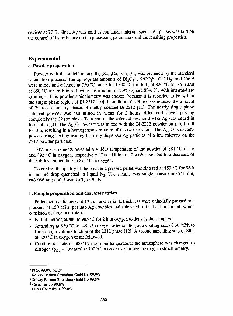
devicesat77 K.SinceAg wasusedas containermaterial,specialemphasiswas laidonthecontrolof its influenceonthe processingparametersandtheresultingproperties.
Experimentala. Powder preparation
Powder with the stoichiometry Biz2SrzoCal.0CuzoOx was prepared by the standardcalcination process. The appropriate amounts of Bi203a , SrCO3b , CaCO3c and CuOawere mixed and calcined at 750 °C for 18h, at 800 °C for 36 h, at 820 °C for 85 h andat 850 °C for 96 h in a flowing gas mixture of 20% 02 and 80% N2 with intermediategrindings. This powder stoichiometrywas chosen, because it is reported to be withinthe single phase region of Bi-2212 [10]. In addition, the Bi-excess reduces the amountof Bi-free secondary phases of melt processed Bi-2212 [11]. The nearly single phasecalcined powder was ball milled in hexan for 2 hours, dried and sieved passingcompletely the 32 l.tmsieve. To a part of the calcined powder 2 wt% Ag was added inform of Ag20. The Ag20 powder_ was mixed with the Bi-2212 powder on a roll millfor 3 h, resulting in a homogeneousmixture of the two powders. The Ag20 is decom-posed during heating leading to finely dispersed Ag particlesof a few microns on the2212 powder particles.
DTA measurements revealed a solidus temperatureof the powder of 881 °C in airand 892 °C in oxygen, respectively.The addition of 2 wt% silver led to a decrease ofthe solidus temperature to 871 °C in oxygen.
To control the quality of the powder a pressed pelletwas sintered at 850 °C for 96 hin air and drop quenched in liquid N2. The sample was single phase (a=0.541 nm,c=3.086 rim)and showed a T c of 95 K.
b. Sample preparation and characterization
Pellets with a diameterof 13 mm and variablethicknesswere uniaxiallypressed at apressure of 150 MPa, put into Ag crucibles and subjected to the heat treatment, whichconsistedof three main steps:
• Partial meltingat 880 to 905 °C for 2 h in oxygento densify the samples.• Annealing at 850 °C for 48 h in oxygen after cooling at a cooling rate of 30 °CPato
form a high volume fraction of the 2212 phase [12]. A second annealingstep of 80 hat 820 °C in oxygen or air followed.
• Cooling at a rate of 300 °C/h to room temperature;the atmosphere was changed to
nitrogen (po2= 10-3atm) at 700 °Cin order to optimizethe oxygen stoichiometry.
a PCF, 99.9% puritybSolvay Barium StrontiumGmbH, > 99.9%c Solvay Barium Strontium GmbH, > 99.9%aCerac Inc., > 99.8%e Fluka Chemika, > 99.0%
383
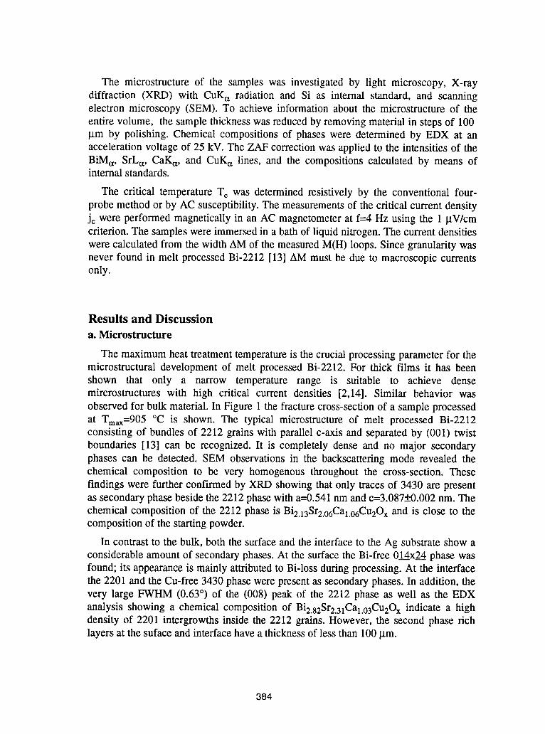
The microstructure of the samples was investigated by light microscopy, X-raydiffraction (XRD) with CuKct radiation and Si as internal standard, and scanningelectron microscopy (SEM). To achieve information about the microstructure of theentire volume, the sample thicknesswas reducedby removingmaterial in steps of 100I.tm by polishing. Chemical compositions of phases were determined by EDX at anacceleration voltage of 25 kV. The ZAF correctionwas applied to the intensities of theBiM_, SrLa, CaKa, and CuK_ lines, and the compositions calculated by means ofinternal standards.
The critical temperature Tc was determined resistively by the conventional four-probe method or by AC susceptibility.The measurementsof the critical current densityJc were performed magnetically in an AC magnetometerat f---4Hz using the 1 _tV/cmcriterion. The samples were immersedin a bath of liquid nitrogen. The current densitieswere calculated from the width AM of the measuredM(H) loops. Since granularity wasnever found in melt processed Bi-2212 [13] AM must be due to macroscopic currentsonly.
Results and Discussiona. Microstructure
The maximum heat treatmenttemperatureis thecrucial processing parameter for themicrostructural development of melt processed Bi-2212. For thick films it has beenshown that only a narrow temperature range is suitable to achieve densemircrostructures with high critical current densities [2,14]. Similar behavior wasobserved for bulk material. In Figure 1 the fracture cross-sectionof a sample processedat Tmax=905°C is shown. The typical microstructure of melt processed Bi-2212consisting of bundles of 2212 grains with parallel c-axis and separated by (001) twistboundaries [13] can be recognized. It is completely dense and no major secondaryphases can be detected. SEM observations in the backscatteringmode revealed thechemical composition to be very homogenous throughout the cross-section. Thesefindings were further conf'trrnedby XRD showingthat only traces of 3430 are presentas secondary phase beside the 2212 phase with a=0.541nm and c=3.087_+0.002nm. Thechemical composition of the 2212 phase is Bi2.13Sra.o6Cal.o6Cu20x and is close to thecomposition of the starting powder.
In contrast to the bulk, both the surfaceand the interfaceto the Ag substrateshow aconsiderable amount of secondaryphases.At the surface the Bi-free 014x24 phase wasfound; its appearance is mainly attributedto Bi-loss during processing. At the interfacethe 2201 and the Cu-free 3430 phase were presentas secondaryphases. In addition, thevery large FWHM (0.63°) of the (008) peak of the 2212 phase as well as the EDXanalysis showing a chemical composition of Bi2.82Sra.31Cal.o3Cu20x indicate a highdensity of 2201 intergrowths inside the 2212 grains. However, the second phase richlayers at the suface and interface havea thicknessof less than 100lam.
384
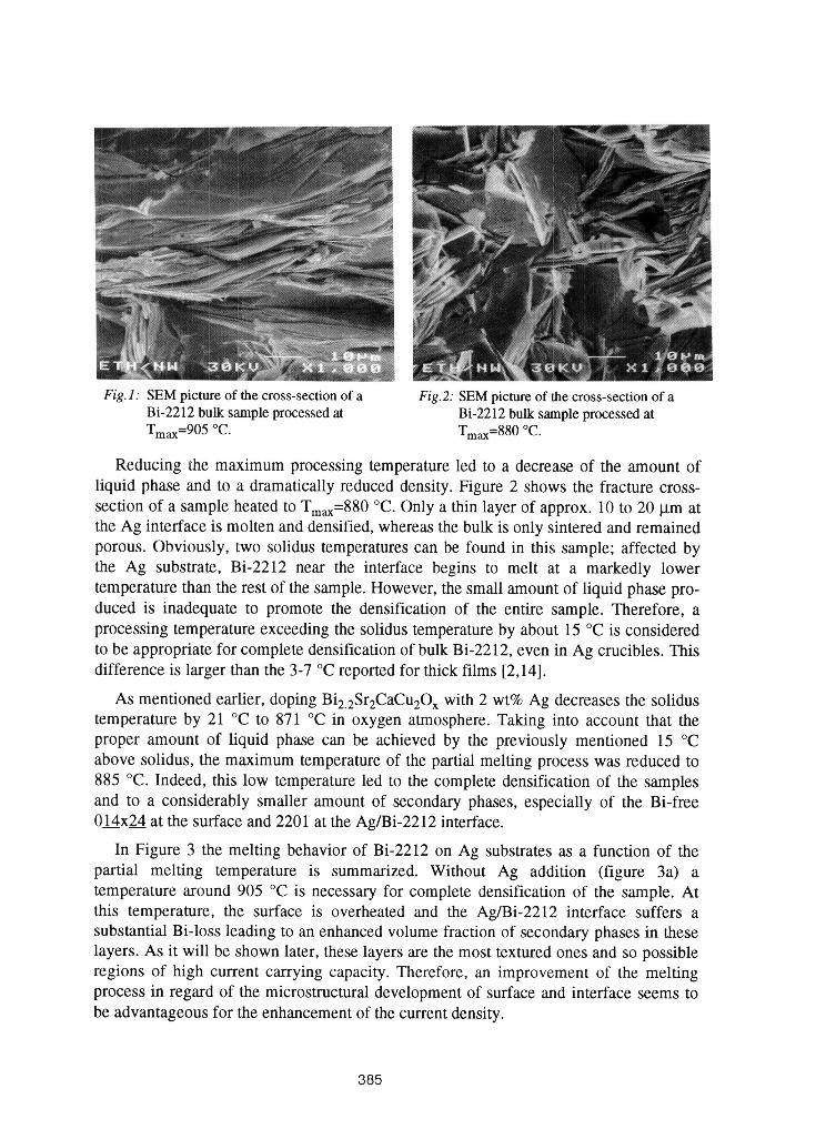
Fig.I: SEM picture of the cross-section of a Fig.2: SEM pictureof the cross-section of aBi-2212 bulk sample processed at Bi-2212 bulksample processed atTmax=905 °C. Tmax=880 °C.
Reducing the maximum processing temperature led to a decrease of the amount ofliquid phase and to a dramaticallyreduced density. Figure 2 shows the fracture cross-section of a sample heated to Tmax=880 °C. Only a thin layer of approx. 10 to 20 l.tmatthe Ag interface is molten and densified,whereas the bulk is only sintered and remainedporous. Obviously, two solidus temperaturescan be found in this sample; affected bythe Ag substrate, Bi-2212 near the interface begins to melt at a markedly lowertemperature than the rest of the sample.However,the small amountof liquid phase pro-duced is inadequate to promote the densification of the entire sample. Therefore, aprocessing temperature exceeding the solidustemperature by about 15 °C is consideredto be appropriate for complete densificationof bulk Bi-2212,even in Ag crucibles. Thisdifference is larger than the 3-7 °Creported for thick films [2,14].
As mentionedearlier, doping Bi2.2Sr2CaCu20x with 2 wt% Ag decreasesthe solidustemperature by 21 °C to 871 °C in oxygen atmosphere. Taking into account that theproper amount of liquid phase can be achieved by the previously mentioned 15 °Cabove solidus, the maximum temperatureof the partial melting process was reduced to885 °C. Indeed, this low temperature led to the complete densification of the samplesand to a considerably smaller amount of secondary phases, especially of the Bi-free014x24 at the surface and 2201 at the Ag/Bi-2212interface.
In Figure 3 the melting behavior of Bi-2212 on Ag substrates as a function of thepartial melting temperature is summarized. Without Ag addition (figure 3a) atemperature around 905 °C is necessary for complete densification of the sample. Atthis temperature, the surface is overheated and the Ag/Bi-2212 interface suffers asubstantial Bi-loss leading to an enhancedvolume fraction of secondary phases in theselayers. As it will be shown later, these layersare the most textured ones and so possibleregions of high current carrying capacity. Therefore, an improvement of the meltingprocess in regard of the microstructuraldevelopmentof surface and interface seems tobe advantageous for the enhancementof thecurrent density.
385
Lowering the maximum processing temperature Tmax to 880 °C does not solve theproblem. The microstructureof the interfacelayer is certainlyimproved, but the amountof liquid phase is insufficient to densify the whole sample. Therefore, such lowtemperatures can only be used for the fabrication of thick films which consist entirelyof Ag/Bi-2212 interface. The second, more promising way to improve the micro-structure of bulk material is the addition of 2 wt% Ag to the powder (figure 3b). Itlowers the solidus temperature of the entire sample and eliminates the inhomogenousmelting. At the same time, the processing temperatureis comparable to the one used forthe partial melting of thick films. Therefore, the volume fraction of secondaryphases atthe interface due to overheating and at the surface due to Bi evaporation can bemarkedly reduced.
(a) withoutAg addition (b) with 2 wt% Ag addition
T=905 °C T=885 °C
Ag substrate
T=880 °C_ g-/zzz_ dense Bi-2212Bi-2212 with
secondary phases
V-----q porous Bi-2212
Fig.3: Schematic drawing of the melting behaviorof Bi-2212bulk samples on Ag substrates(a) without and (b) with 2 wt% Ag addition.
b. Texture
Figure 4 shows the dependence of the degree of texturea on the distance from theAg/Bi-2212 interface. The high value of f=0.99 at the interface expresses an almostperfect alignment of the (ab)-plane parallel to the Ag substrate. However, the highlytextured layer has only a thickness of less than 100 I.tm. Comparable good grainalignment is found at the samplesurface.
a Quantification of the texture from XRD measurement:f = ]_Intensities(001)2212/Elntensities(hkl)z212
386
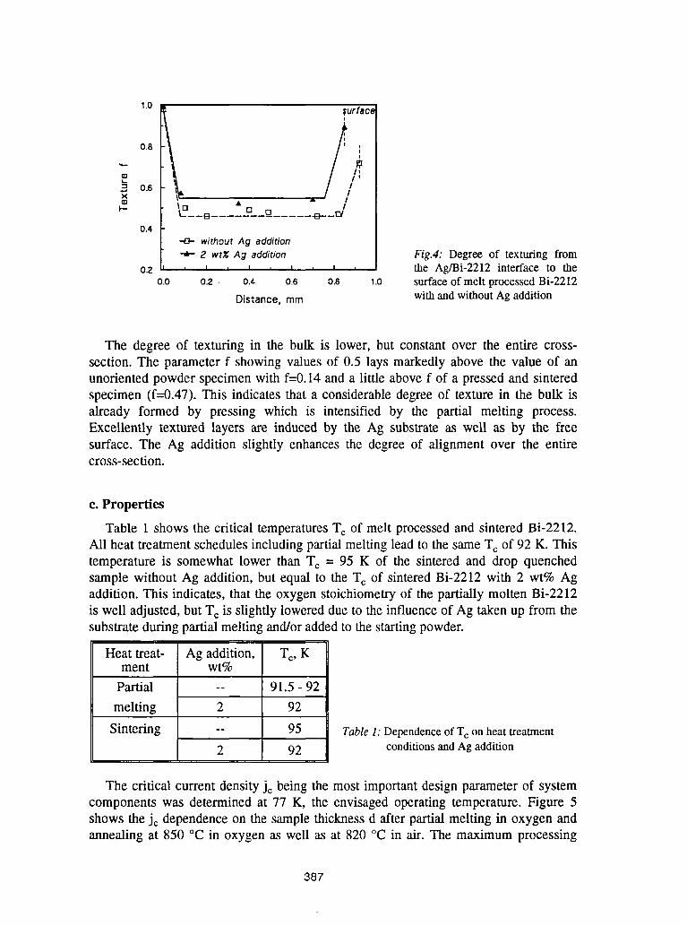
1.0 _urfacei
_--_ 0.8 t2 o.6x I
_ • I----B O O ___
0.4
without Ag addition
2 wt_ Ag addition Fig.4: Degree of texturing from0.2 , _ , _ , _ , _ , the Ag/Bi-2212 interface to the
o.o 0.2 . 0.4 o6 0.8 1.o surface of melt processed Bi-2212with and without Ag additionDistance, mm
The degree of texturing in the bulk is lower, but constant over the entire cross-section. The parameter f showing values of 0.5 lays markedly above the value of anunoriented powder specimen with f=0.14 and a little above f of a pressed and sinteredspecimen (f=0.47). This indicates that a considerable degree of texture in the bulk isalready formed by pressing which is intensified by the partial melting process.Excellently textured layers are induced by the Ag substrate as well as by the freesurface. The Ag addition slightly enhances the degree of alignment over the entirecross-section.
c. Properties
Table 1 shows the critical temperatures Tc of melt processed and sintered Bi-2212.All heat treatment schedules including partial melting lead to the same Tc of 92 K. Thistemperature is somewhat lower than Tc = 95 K of the sintered and drop quenchedsample without Ag addition, but equal to the Te of sintered Bi-2212 with 2 wt% Agaddition. This indicates, that the oxygen stoichiometry of the partially molten Bi-2212is well adjusted, but Tc is slightly lowered due to the influence of Ag taken up from thesubstrate during partial melting and/or added to the starting powder.
Heat treat- Ag addition, Tc, Kment wt%
Partial -- 91.5 - 92
melting 2 92
Sintering -- 95 Table1:DependenceofTc onheattreatment2 92 conditionsandAg addition
The critical current density Jc being the most important design parameter of systemcomponents was determined at 77 K, the envisaged operating temperature. Figure 5shows the Jc dependence on the sample thickness d after partial melting in oxygen andannealing at 850 °C in oxygen as well as at 820 °C in air. The maximum processing
387
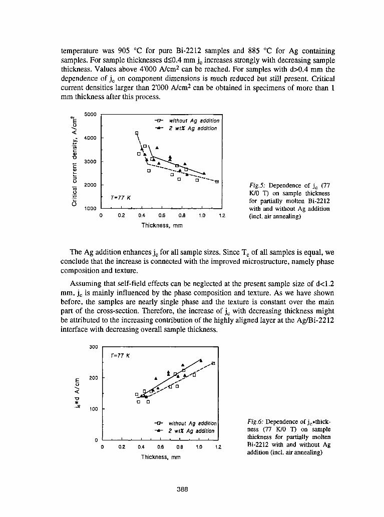
temperature was 905 °C for pure Bi-2212 samples and 885 °C for Ag containingsamples. For sample thicknessesd<0.4 mm Je increasesstrongly with decreasing samplethickness. Values above 4'000 A/cm2 can be reached. For samples with d>0.4 mm thedependence of Je on component dimensions is much reduced but still present. Criticalcurrent densities larger than 2'000 A/cm2 can be obtained in specimens of more than 1mm thicknessafter this process.
5000
_ without Ag addition(.3
-_- E wt% Ag addition< q
- 4000 \
- []E 3000L--
2000 Fig.5: Dependence of Je (77t_
.u_ K/0 T) on sample thickness"-" T=77 Kx-O for partially molten Bi-2212
looo , T , , , t , , , T , with and without Ag addition0 0.2 0.4 0.6 0.fl 1.0 1.2 (incl. air annealing)
Thickness,mm
The Ag addition enhancesJcfor all samplesizes. SinceTc of all samples is equal, weconclude that the increase is connectedwith the improvedmicrostructure,namely phasecomposition and texture.
Assuming that self-field effects can be neglectedat the present sample size of d<l.2mm, Jc is mainly influenced by the phase composition and texture. As we have shownbefore, the samples are nearly single phase and the texture is constant over the mainpart of the cross-section. Therefore, the increase of Jc with decreasing thickness mightbe attributed to the increasing contributionof thehighly alignedlayer at the Ag/Bi-2212interface with decreasingoverall sample thickness.
300
T=77 K
tE 200 •o 3
< n
, [] ou
lot
--o- without Ag addition Fig.6: Dependence ofje,thick-2 wtZ Ag addition ness (77 K/0 T) on sample
0 , , , , , , , t , , , thickness --Iorpartially molteno 02 0.4 0.B O.8 1.0 1.2 Bi-2212 with and without Ag
addition (incl. air annealing)Thickness,rnm
388
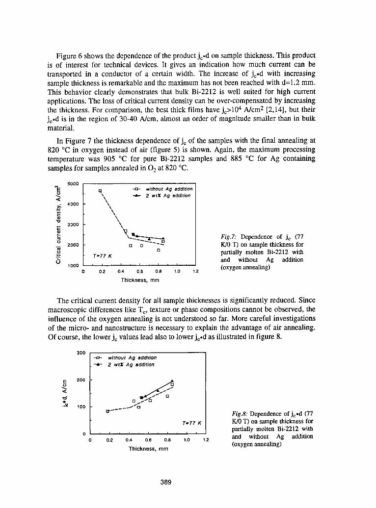
Figure 6 shows the dependenceof the productje,d on sample thickness.This productis of interest for technical devices. It gives an indication how much current can betransported in a conductor of a certain width. The increase of jc,d with increasingsample thickness is remarkableand the maximumhas not been reached with d=l.2 mm.This behavior clearly demonstrates that bulk Bi-2212 is well suited for high currentapplications. The loss of critical current densitycan be over-compensatedby increasingthe thickness. For comparison, the best thick films have jc>104A/cm2 [2,14], but theirjc,d is in the region of 30-40 AJcm, almost an order of magnitudesmaller than in bulkmaterial.
In Figure 7 the thickness dependenceof Jcof the sampleswith the final annealingat820 °C in oxygen instead of air (figure 5) is shown. Again, the maximum processingtemperature was 905 °C for pure Bi-2212 samples and 885 °C for Ag containingsamplesfor samples annealed in O2at 820 °C.
5000
_E I_ -0- without Ag additiono \ -a,- 2 wtX Ag addition< \
4000 \\-_ \r- \
"1o \3000 \
E \_t3
_v._ Fig.7: Dependence of Jc (77zooo o D..... K/0 T) on sample thickness for
to r'lt_ partially molten Bi-2212 with"_ T=77 Ko and without Ag addition
1ooo ........... ( aling)oxygen anne0 0.2 0.4 0.8 0.8 1.0 1.2
Thickness, mm
The critical current density for all sample thicknessesis significantlyreduced. Sincemacroscopic differences like To, texture or phase compositionscannot be observed, theinfluence of the oxygen annealing is not understoodso far. More careful investigationsof the micro- and nanostructureis necessary to explain the advantage of air annealing.Of course, the lowerj_ values lead also to lowerjc,d as illustratedin figure 8.
300--o- without Ag addition
-a- 2. wt_[ Ag addition
E 200
""_ 100 [_'_------_"OFig.& Dependence of je,d (77
r=z7 K K/0 T) on sample thickness forpartially molten Bi-2212 with
0 i I = [ i I i I = I iand without Ag addition0 0.2 0.4 0.6 0.B 1.0 1.2
(oxygenannealing)Thickness. mm
389
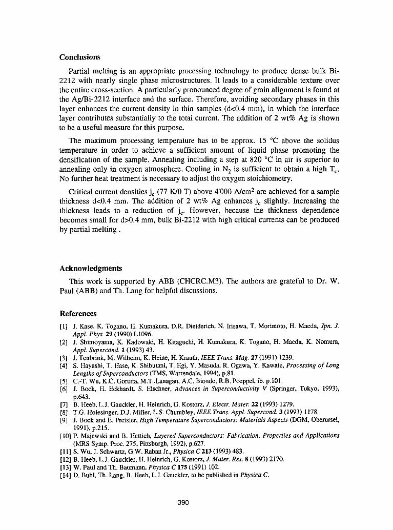
Conclusions
Partialmeltingis an appropriateprocessingtechnologyto producedense bulk Bi-2212 with nearly single phasemicrostructures.It leads to a considerabletextureoverthe entirecross-section.A particularlypronounceddegreeof grainalignmentis foundatthe Ag/Bi-2212 interfaceand the surface.Therefore,avoidingsecondaryphasesin thislayerenhances the currentdensityin thin samples(d<0.4 ram), in which the interfacelayer contributes substantially to the total current. The addition of 2 wt% Ag is shownto be a useful measure for this purpose.
The maximum processing temperature has to be approx. 15 °C above the solidustemperature in order to achieve a sufficient amount of liquid phase promoting thedensification of the sample. Annealing including a step at 820 °C in air is superior toannealing only in oxygen atmosphere.Cooling in Nz is sufficient to obtain a high Tc.No further heat treatmentis necessary to adjust the oxygen stoichiometry.
Critical current densitiesJc (77 K/0 T) above 4'000 A/cm2 are achieved for a samplethickness d<0.4 mm. The addition of 2 wt% Ag enhancesJc slightly. Increasing thethickness leads to a reduction of Jc. However, because the thickness dependencebecomes small for d>0.4 mm, bulk Bi-2212with high critical currents can be producedby partial melting.
Acknowledgments
This work is supported by ABB (CHCRC.M3). The authors are grateful to Dr. W.Paul (ABB) and Th. Lang for helpful discussions.
References
[l] J. Kase, K. Togano, H. Kumakura, D.R. Dietderich, N. Irisawa, T. Morimoto, H. Maeda, Jpn. J.Appl. Phys. 29 (1990) L1096.
[2] J. Shimoyama, K. Kadowaki, H. Kitaguchi, H. Kumakura, K. Togano, H. Maeda, K. Nomura,Appl. Supercond. 1 (1993) 43.
[3] J. Tenbrink, M. WilheLm, K. Heine, H. Krautla, IEEE Trans. #lag. 27 (1991) 1239.[4] S. Hayashi, T. Hase, K. Shibutani, T. Egi, Y. Masuda, R. Ogawa, Y. Kawate, Processing of Long
Lengths of Superconductors (TMS, Warrendale, 1994), p.81.[5] C.-T. Wu, K.C. Goretta, M.T.,Lanagan, A.C. Biondo, R.B. Poeppel, ib. p.10l.[6] J. Bock, H. Eckhardt, S. Elschner, Advances in Superconductivity V (Springer, Tokyo, 1993),
p.643.[7] B. Heeb, L.J. Gauckler, H. Heirtrich, G. Kostorz, J. Electr. Mater. 22 (1993) 1279.[8] T.G. Holesinger, D.J. Miller, L.S. Chumbley, IEEE Trans. AppL Supercond. 3 (1993) 1178.[9] J. Bock and E. Preisler, High Terapeiature Superconductors: Materials Aspects (DGM, Oberursel,
1991), p.215.[10] P. Majewski and B. Hettich, Layered Superconductors: Fabrication, Properties and Applications
(MRS Syrup. Proc. 275, Pittsburgh, 1992), p.627.[11] S. Wu, J. Schwartz, G.W. Raban Jr., Physica C 213 (1993) 483.[12] B. Heeb, L.J. Gauckler, H. Heinrich, G. Kostorz, J. Mater. Res. 8 (1993) 2170.[13] W. Paul and Th. Baumann, Physica C 175 (1991) 102.[14] D. BuM, Th. Lang, B. Heeb, L.J. Gauckler, to be published in Physica C.
390
N MAKJet al. Proceedings4th WorldCongressonSuperconductwrty,Orlando,FIolida(1994)
CORRELATIONBETWEENFABRICATIONFACTORAND SUPERCONDUCTING
PROPERTIESOF
THE TL- AND BI- BASEDHIGH-Tc SUPERCONDUCTOR
Naoki MAKI,Michiya OKADA,Toshiya J. DOI,Tsuneyuki KANAI,
Jun'ichiSATO',
and KazutoshiHIGASHIYAMA
Hitachi ResearchLaboratory,Hitachi Ltd.
Ohmika-cho7-1-1,Hitachi, Ibaraki319-12Japan
*AdvancedResearchLaboratory,Hitachi CableLtd.
Kidamari-cho3550, Tsuchiura,Ibaraki300Japan
ABSTRACT
Largecriticalcurrentdensities(Jc)were obtainedinc-axisorientedTI-1223/Agcompositetapesfabricatedby spraying
methodswithouta vacuum.Transportmeasurementsat 77Kundera zerofieldindicateda Jc of9x10' AJcm2and7x 103Ncmz at
1T forthe tapesfabricatedbyspraypyrolysis.The novelGPM methodwasalsoappliedforBi-2212/AgPiT compositewire,and
found to beveryeffectiveforimprovingthedistributionofvoids,whichcausedfromthemelt-solidifyingprocess.TheGPMshowed
a markedeffect forobtaininghomogeneouslongwire. A IT classcoilwassuccessfullyfabricatedwithmonocorewire.
1. INTRODUCTION
It is well known that the Bi-systemwires with high critical current densityJc's are much
preferable for applications in high magnetic field regionsat cryogenic temperature below 20K than
TI-systemsuperconductorsfrom the viewpointof processeasiness realizing good crystal alignment
enabling a large current flow, however, the Bi-systemsuperconductorscan not be useful in liquid
nitrogen temperature applications due to the weak pinning characteristics caused from the two
dimensional vortex structure. In the latter case, T1-1223with Tc 122K, having strong pinning
characteristics (with more three dimensional vortex structure), is thought to be the best candidate.
Since, T1-1223requires ,however, the three-dimensionalcrystal alignment for overcoming the grain
boundary weak links, the wire fabrication processesare thought to be restricted in a field of the
thin film technologies.
In thispaper, weshow the following two novel processingfor bothBi- andTI- system HTS's,
(1) GPM( gas pressurizedmelt) processfor Bi-2212/Ag solenoidcoil usingPIT
(2) Spray pyrolysis method for T1-1223on silver substratein ambient pressureconditions.
391
N. MAKJ et al.. Proceedings 4th Wodd Congress on SuperconductJvity, Orlando Flolida (1994)
2. Bi-2212 GPM Process
It is well knownthe Bi-2212/Agwire with high criticalcurrentdensityJc can easily be
obtainedthroughthe partial-meltingprocess." However,the mostseriousproblemof the processis
thoughtto be the oxygenreleasewhichcauses"swelr onthewire.So far, we havealreadyreported
that the oxygen release can be reduced using the Bi-2212 powderswith Ag,2_calcined at
temperaturesaroundmeltingpoint,undera highoxygenpartialpressure(100% 02 - 1 atrn). Inorder
to achievea goodsuperconductingpropertyina longwire, itis necessaryto improvernicrostructural
homogeneityin the longitudinaldirectionof the wire. In followings,we will discussthe effect of the
GPM (Gas PressurizedMeltProcess)for Bi-2212/Ag,onmicrostructure.3_
2.1 Experimental
Commercialpowdersof 3N pureoxidewere mixed in a nominalcompositionof Bi2Sr2 Ca1
Cu2Ago20y and calcinedtwiceat810°C for 10h. Silvertubeswithouterdiameterof 6ram,filledwith
the powder,were processedbydrawing to get 0.7mm and 1.2mmouterdiameterand25m length
wires.The roundwirewascutinto3cmlengthsfor shortsample. As-drawing25m longwires(l.2mm
o.d.) werewoundintosolenoidtype. The fabricatedsolenoidcoilis shownin Fig.l. Bothshortwires
andthe coilswere partiallymeltedfor 10 minutesfrom 865°C to 885°C. Shortwireswerecalcined
undervariousconditionsof oxygenconcentrationandtotalgas pressure.Coils were meltedunder
bothatmosphericpressureanda pressurizedatmosphere,usingGPM. The transportcriticalcurrent
wasmeasuredby a four-probemethodat 4.2K witha 1 u.V / cm criterionfor short wires,andwitha
1013Q • m criterion for coils. The voids distributioninside Ag-sheathwas observed using X-ray
radiography (Voltage : 180kV,current : 5mA, target : W ).
2.2 Results and discussion
Since the oxygen partial pressureduringmelt processaffect a releaseof oxygengas from
Bi-2212 crystals,oxygenpartial pressure,PO2,should be changedto appear the effect on void
formationand superconductingproperties.It was found that the high Jc valuesof over 105A/cm2
were obtainedusingGPM undera pO2 of 1.0 to 3.0 atm. And, we investigatedthe detailsof the
effect of totalgas pressureunderthe conditionof pO2=1.0._1.2atm. Underthe total gas pressure
over 3.0 atm witha constantpO2,relativelyhighJc valuesareobtainedina widetemperaturerange
witha littlescatterings.Accordingto the X-ray radiography,the distributionof voidsinwires melted
at Pro=, of 6.0 atrn estimatedto be smaller than those of melted at the atmosphericpressure
(Pro=,=1.0atrn) .Therefore,the GPM methodwhichmeltedunderpO2 of 1.0 to 3.0 atm and Ptotal
over 3.0 atm, are prerequisitesfor gettingwires with the high Jc values and homogeneous
distributionof voids. We also fabricated small solenoidcoilsmeltedunder both ambient and the
GPM atmosphere.Fig.2 showsthe distributionof voids in both coils. Horizontalaxis showsthe
average length of the voidsin the longitudinaldirectionof the wire, and vertical axis showsthe
numberof the voids.The propertiesof the coilmeltedundertheatmosphericpressureare markedly
dependson the cross-sectionallocations.For example,outer-mostside, the Jc was lowest,which
392
N MAIKJet al Proceedings 4th World Congress on Superconduc'bvity. Orlando. Flolida (1994)
correspondstothe void concentrationof 50 mm long in fig.2. Microstructuresand Tc of the coil were
homogeneous,however,the distribution of the voids governed the V-I properties.On the other hand,
voids of the coil processedthroughthe GPM method were 10mmlong at most. Therefore, the GPM
method seems to be very effective for improving the distribution of voids, and makes easy for
obtaining homogeneous long wire. The coil, using a 5 pieces of 25m long wire, generated a
maximum magnetic field of 1.1Tat a current of 88A.
3. TIo1223/Ag composite tape
In order to apply high-Tc superconductorsto magnets operable in liquid nitrogen, a
considerablelengthof wiremustbe fabricatedwitha transportJc of at least10' AJcm2in magnetic
fieldsof 1 T orgreater.Keyto the fabricationof practicalhigh-Tcsuperconductingwiresisto prepare
polycrystallineconductorswhich have good intergranularconnectivityand high flux pinning
characteristics.AlthoughYBCO'> and T1-12235_7>has strongpinningforce at 77K, the transport
capabilitiesof wires fabricatedby the powder-in-tubemethodare seriouslyimpairedby weak-link
behaviorresultingfrom poor intergranularconnectivity.In contrast,largetransportJc valueshave
been reportedfor YBCO thin films epitaxiallygrownon oxidesinglecrystals8_and even for those
grownon metalwith a biaxialalignedbufferlayer9_by physicalor chemicalvapordeposition.It is
importantto alignthe in-planea- andb-axesof individualgrainsbyusingthinfilm processesinorder
to inhibit weak-link behavior. Such processes,however, which must be performed under
high-vacuumconditions,may not be suitable for wire applications,where long length, high
productivityandlowcostare required.
The spray pyrolysismethodis a film fabricationtechniquewhichdo notrequirea vacuum,
andwhichthereforemake it possibleto producelonglengthsof tape shapedwires.Inthispaper,we
report a high Jc value for TI-based superconductors/Agcompositetapes preparedby spraying
methodsunderambientpressure,thusverifyingthe highpotentialof thesemethods.
3.1 Experimental
The precursorfilms containingappropriateproportionsof all the metals except TI were
depositedunderambientpressure.The depositedfilms are porous,and so they were pressedor
rolledto make themdenserandthen firedina controlledthalliumoxidevapor.
Forthespraypyrolysis,a 0.02 mol/IaqueoussolutionwaspreparedfromBa(NO3)2,Sr(NO3)2,
Ca(NO3)2.4H20andCu(NO3)2.3H20witha metalstoichiometricratioof Ba:Sr:.Ca:Cu=l.6:0.4:2:3.The
spraysolutionwas convertedintoa mistwith an ultrasonictransducer.The mistwasintroducedonto
the Ag tape whichwasheatedto 700°C.Thedepositedprecursoroxidefilmswere fired at 860°C for
30 hoursina controlledthalliumoxidevapor.Thefilmthicknesswasapproximately1 _Jm.
The transportJc of the filmswasmeasuredbyusingthestandardfourprobemethodwitha
criterionof 1LLV/cm. ThecrystalstructureandcompositionwereanalyzedbyX-raydiffraction(XRD)
and energy-dispersiveX-ray analysis(EDX). Their microstructurewas observedwith a scanning
electronmicroscope(SEM) andX-raypole-figureanalysis.
393
N MAKIetal. • Proceedings4th WorldCongressonSuperconductlvrty,Orlando,Flolida(1994)
3.2 Results and discussion
Figure 3 showsthe XRD pattern of TI-1223/Agcompositetape prepared by the spray pyrolysis
method. All the peaks can be assigned to the (001)diffraction of the T1-1223phase, except for the
(hkl) diffraction of Ag metal. The film was confirmed to consist of single phase T1-1223with c-axis
crystal orientation.The specimen for Jc measurementswas cut from the 1 m long composite tape.
The Jc variation was within 5 % for all the pieces.The highest Ic value of any samplewas 6.0 A and
its Jc was 9x10⁴ A/cm2 at 77 K without a magnetic field. Figure 4 shows the magnetic field
dependenceof the TI-1223/Ag composite tape with the field applied parallel to the c-axis. The Jc at
1T was 7x10³A/cm2which is 10 times the value of our silver sheathedT1-1223wire. To improve the
Jc for practical high-Tc superconductingwire, it is importantto achieve three dimensional alignment
of the in-plane a-axes (biaxialorientation)of individualT1-1223grains.
Recently we have found that biaxially oriented T1-1223films can be successfully formed on a
SrTiO3(100) single crystal substrate by spray pyrolysis. Figure 5 shows the magnetic field
dependenceof Jc for T1-1223film with the field applied parallel and perpendicularto the c-axis up to
8T at 77K. The curves reveal a relatively weak dependenceunder low fields. When the fields were
applied parallel to the c-axis, Jc reached5x104Ncm 2at 1T.The gentle magnetic field dependenceof
Jc below 1T for the biaxial oriented T1-1223film suggests that the weak-link problem is almosteliminated in the film.
To achieve biaxial orientation in TI-1223/Agcompositetapes, the "buffer layer" or "metal substrate"
itself have to be aligned biaxially, lijima et al.9_reportedthe successfulgrowth of a biaxially aligned
YSZ buffer layer on a hastelloy substrate by the ion-beamassisteddeposition process,and biaxially
aligned YBCO films with hightransportJc valueswere formed on it.
YBCO films grown by the laser ablation method on Ag(001), Ag(110) and Ag(111) single crystal
substrates show specific in-plane epitaxial orientationwith respect to the crystallographicaxes of the
substrate_°1.This result has important consequences in terms of in-plane alignment on metal
substrates. It is well known that a (100)[001] texture can be easily formed by rolling and annealing
with fcc metals suchas Cu where the metal surface consistsof a square arrangementof atoms. In
the case of Ag, the annealed texture is different from that of Cu, which is mainly (110)[112] and
which is described as a rectangular lattice. Yoshinoet al.TMshowedthat YBCO films grown on a (110)
textured Ag substrate by ionized-cluster-beam-deposition,were aligned with in-plane orientation.
However, this textured substrate was not suitable for use with our spraying method because of its
instability of texture and surface irregularityat higher temperature.We examinedthe optimum rolling
and annealing conditions with which to obtain the (100) texture. Figure 6 shows the XRD (8-28)
pattem and surface morphorogy of the nearly (100) textured Ag substrate. The texture and surface
flatness of the Ag substrate remainedeven at 850°C which correspondsto the heating temperature
for the precursorfilms.
The results of this study demonstrate the considerable potential of the spray pyrolysis method,
which does not require a vacuum, for the fabrication of practicalsuperconductingwires and tapes.
394
N. MAKIet al. Proceedings4th World CongressonSuperconductivity,Orlando,Flolida(1994)
4. Acknowledqments
The authorswould like to thank Dr.K.Aiharaof Hitachi ResearchLaboratoryfor usefuldiscussions.
5. References
1)J. Kase,K. Togano, H. Kumakura,D. R. Dietderich,N. Irisawa,T. Morimotoand H. Maeda : Jpn. J.
Appl.Phys.29 (990) L1096.
2)T.Kanai and T. Kamo : Supercond.Sci. Technol.6(1993)510.
3)T.Kanai and N.Inoue : J. Mat. Sci. :to be published
4) M. Murakami, M. Morita, K. Doi, K. Miyamoto andH. Hamada:Jpn. J. Appl. Phys. 28 (1989) L339.
5) D. H. Kim, K.E.Gray, R. T. Kampwirth, J. C. Smith, D. S. Richeson, T. J. Marks and M. Eddy:
Physica C 177(1991)431.
6) T. J. Doi, M. Okada, A. Soeta, T. Yuasa, K. Aihara, T. Kamo and S. Matsuda: Physica C 183
(1991)67.
7) R. S. Riu, D. N. Zheng, J. W. Loren, K. A. Mirza, A. M. Campbell and P. P. Edwards:Appl. Phys.
Lett. 54 (1989) 760.
8) B. Roas et al.: Appl. P. on Superconductivity(ISS '93), Hiroshima,October, 1992p119.
9) Y. lijima, N. Tanabe,O. KohnoandY. Ikeno:Appl. Phys. Lett. 60 (1992)769.
10) J. D. Budai, R. T. Young and B. S. Chao:Appl. Phys. Lett. 62 (1993)1836.
11) H. Yoshino, M. Yamazaki, H. Fuke, T. D. Thanh, Y. Kudo, K. Ando and S. Oshima: Abstracts of
6th Int. Symp. on Superconductivity,Hiroshima,October, 1992,p119.
395
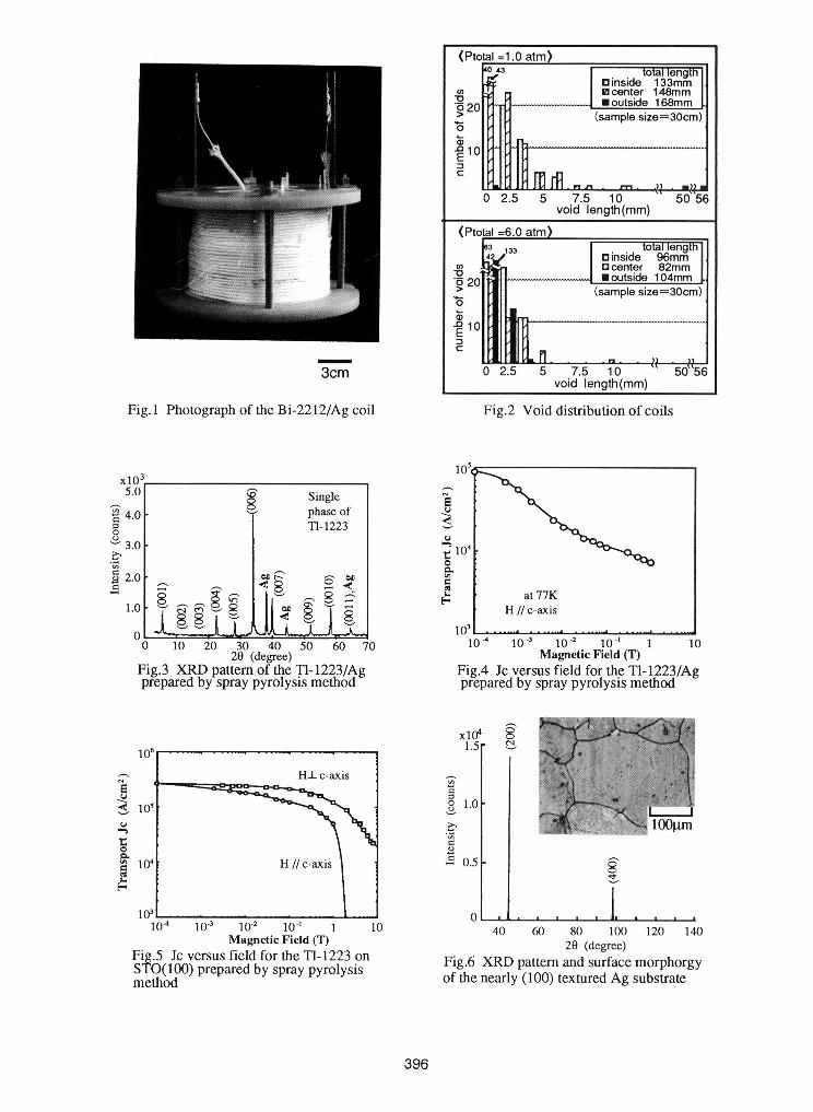
(Ptotal =1.0 atm)
o43 J totallength
[] inside 133mm
._ ! ==center 148mm. ==outside168mm
(samplesize=3Ocm)
J-i . m . 3) . ==)) ==
0 2.5 5 7.5 10 "" 50"5Evoid length(mm)
Ptotal =6.0 atm}33
m
3cm 0 2.5 5 7.5 10void length(mm)
Fig. 1 Photograph of the Bi-2212/Ag coil Fig.2 Void distribution of coils
xlO:
5.0 _" Single4.0 ,_ phase of
o _ _, T1-1223 __ 3.0 '_ 104
2.0 .-. IV _ s __ _ ,-., _ .. _ at77K
1.0 "-" _ _ .-, .,_=0 v ,. H//c-axis
lOs ......................................0 10 20 30 40 50 60 70 10 _ 10 -3 10-2 10 -t 1 10
20 (degree) Magnetic Field (T)Fig.3 XRD pattern of the Tl-1223/Ag Fig.4 Jc versus field for the Tl-1223/Agprepared by spray pyrolysis method prepared by spray pyrolysis method
xlOa1.5
106 ......
HI c-axis
10_ 8 1.0
_ 100txm
10, _ 0.5I
l(P 0 ...... l .....104 10.3 102 10 -1 1 10 40 60 80 100 120 140
Magnetic Field (T) 20 (degree)Fig.5 Jc versusfieldfor theT1-1223onSTO(100) prepared by spray pyrolysis Fig.6 XRD pattern and surface morphorgymethod of the nearly(100) texturedAg substrate
396

Index

INDEX
AAgrawal, Bal K........................................................................................................... 300, 555Agrawal, Savitri .......................................................................................................... 300, 555Aldinger, Fritz ................................................................................................... 483, 490, 677Alzayed, N......................................................................................................................... 743Angus, V................................................................................................................... 423, 470Anischenko, S. E....................................................................................................... 574, 585Apaja, V.................................................................................................................... 209, 308Apte, P. R.......................................................................................................... 241,762, 770Amdt, G. Dickey ............................................................................................................... 158Arutyunov, K. Yu .............................................................................................................. 359Atlan, D............................................................................................................................. 470Azuma, M.......................................................................................................................... 529
BBalachandran, U................................................................................................................ 639Balint, A............................................................................................................................ 730Bankuti, J ........................................................................................................................... 730Baumann, Philip D............................................................................................................. 400Baziljevich, M.................................................................................................................... 106Beales, T. P........................................................................................................................ 650Bencze, Laszlo ............................................................................................................. 56, 126Bestgen, H......................................................................................................................... 677Bhalla, A. S........................................................................................................................ 188Bhasin, K. B....................................................................................................................... 611Bhatnagar, A. K ................................................................................................. 241,762, 770Bingham, W. G.................................................................................................................. 410Bona, Maurizio .................................................................................................................... 65Borjesson, L....................................................................................................................... 328Bratsberg, H....................................................................................................................... 106Brinkmann, D...... .............................................................................................................. 273Buhl, D...................................................................................................................... 685, 753
CCardona, M ........................................................................................................................ 328Chaikovsky, V. I................................................................................................................ 574Chakoumakos, B. C........................................................................................................... 347Chen, C. M........................................................................................................................ 694Chorey, C. M..................................................................................................................... 611Christen, D. K.................................................................................................................... 347Chrzanowski, J ........................................................................................................... 423, 470Chu, Wei-Kan .................................................................................................................... 157Cluff, J. A.......................................................................................................................... 633Collings, E. W.................................................................................................................... 138Coy, M.............................................................................................................................. 372Cragg, A. R........................................................................................................................ 450Cragg, R. A................................................................................................................ 423, 470Crapo, Alan ....................................................................................................................... 158Curzon, A. E ...................................................................................................................... 423
DD'Souza, C. P..................................................................................................... 243, 762, 770Danilova, N. P.................................................................................................................... 359Denisov, A. G.................................................................................................................... 568Dhar, S. K.......................................................................................................................... 284Doi, Toshiya J .................................................................................................................... 391
EEichelberger, B. Davis, III .................................................................................................. 198Elifritz, Thomas Lee .......................................................................................................... 500Elschner, S......................................................................................................................... 677Enisz, M............................................................................................................................ 712Ewert, S............................................................................................................................. 460
FFan, Chang-Xin ................................................................................................................. 594Fei, X................................................................................................................................. 743Fife, A. A........................................................................................................... 423, 450, 470Foster, Charles ................................................................................................................... 158Frenck, H. J ....................................................................................................................... 460Fu, C. M.................................................................................................................... 694, 703Fu, C. M.
GGasumyants, V. E...................................................................................................... 356, 537Gauckler, L. J .................................................................................................... 382, 685, 753Geerkens, A....................................................................................................................... 460Giber, J .............................................................................................................................. 116Gobl, Nandor ............................................................................................................... 56, 126Godart, C........................................................................................................................... 284Goretta, K. C .............................................................................................................. 633, 661Gou, Y. S................................................................................................................... 694, 703Grant, P. D......................................................................................................................... 450Greaves, C .......................................................................................................................... 546Guo, Ruyan ....................................................................................................................... 188Guo, Y............................................................................................................................... 743Gupta, L. C........................................................................................................................ 284
I-IHabib, F............................................................... ...................................................... 423, 470Hahakura, S....................................................................................................................... 510Halasz, I............................................................................................................................. 116Haldar, Pradeep ......................................................................................................... 624, 639Han, S. G........................................................................................................................... 594Havenhill, A...................................................................................................................... 743Hawsey, Robert A.............................................................................................................. 624He, W. S............................................................................................................................. 743Heeb, B .............................................................................................................. 382, 685, 753Heinrich, B........................................................................................................ 423, 450, 470Hetland, P. O..................................................................................................................... 106Higashiyama, Kazutoshi ..................................................................................................... 391Hirabayashi, H..................................................................................................................... 75Hiroi, Z...................................................................................................................... 510, 529Hoehn, J. G., Jr.................................................................................................................. 639
Hong, Gye-won ..................................................................................................................... 3Horvath, E ........................................................................................................................... 56Hossain, Zakir .................................................................................................................... 284
IIhara, N............................................................................................................................. 337Irwin, J. C.................................................................................................................. 423, 470Ishida, K............................................................................................................................ 529Iyer, A. N.......................................................................................................................... 639
JJeng, W. J ........................................................................................................................... 703Jennings, R. A.................................................................................................................... 546Johansen, T. H................................................................................................................... 106Joo, J ................................................................................................................................. 633Juang, J. Y................................................................................................................. 694, 703
KKaesche, Stefanie ............................................................................................................... 490Kallio, A.................................................................................................................... 209, 308Kamyshin, V. V, ................................................................................................................ 574Kanai, Tsuneyuki ............................................................................................................... 391Kaufmann, H. J .................................................................................................................. 232Kawashima, T .................................................................................................................... 522Kazanskiy, S. V................................................................................................................. 356Khabayev, P. V.......................................................................................................... 574, 585Kimball, Foster .................................................................................................................. 416Kirschner, I ............................................................................................................ 48, 56, 116Kishio, K........................................................................................................................... 510Kitaoka, Y.......................................................................................................................... 529Kitazawa, K........................................................................................................................ 510Kiuchi, M.......................................................................................................................... 337Kotsis, I............................................................................................................................. 712Kudeliya, A. M.................................................................................................................. 568Kuk, I1-Hyun......................................................................................................................... 3Kumar, A. Anil .................................................................................................................. 601Kumar, D........................................................................................................................... 770Kyotani, Yoshihiro ....................................................................................................... 96, 167
LLanagan, M. T ................................................................................................................... 633Lang, Th .................................................................................................................... 685, 753Larkin, S. Y............................................................................................................... 574, 585Lemanov, V. V.................................................................................................................. 180Leone, A............................................................................................................................ 372Levy-Clement, C................................................................................................................ 284Li, Jiang ............................................................................................................................. 601Lieurance, Dennis .............................................................................................................. 416Lin, H. C............................................................................................................................ 694Lighthipe, R. W.................................................................................................................. 410Litvinchuk, A. P................................................................................................................. 328Liu, Jianxiong .................................................................................................................... 158
Liu, R. S.............................................................................................................................. 10Lu, D. F....................................................................................................................... 60, 594Lucas, M. S. P.................................................................................................................... 743
MMajewski, Peter .................................................................................................. 483, 490, 677Maki, Naoki ....................................................................................................................... 391Matheisen, Axel ................................................................................................................... 84Matsui, Y........................................................................................................................... 522Matsushita, T..................................................................................................................... 337Mazumdar, Chandan .......................................................................................................... 284McCormack, J. S................................................................................................................ 650Meilikhov, E. Z .................................................................................................................. 318Meng-Burany, S................................................................................................................ 423Meszaros,, C....................................................................................................................... 730Meven, M.......................................................................................................................... 460Miller, D. J......................................................................................................................... 661Miranda, F. A.................................................................................................................... 611Mishra, V. K........................................................................................................................ 24Moon, F. C........................................................................................................................ 148Motowidlo, Leszek R................................................................................................. 624, 639Multani, Manu ..................................................................................................................... 24
NNagarajan, R...................................................................................................................... 284Naugle, D. G...................................................................................................................... 222Nikolaeva, A. A................................................................................................................. 359
OObot, Victor ....................................................................................................................... 158Okada, Michiya ................................................................................................................. 391Oltarzhevskaya, Yelena T................................................................................................... 739Oravetz, D.......................................................................................................................... 712Orlova, T. S....................................................................................................................... 232Ossandon, J. G................................................................................................................... 347Ozhogin, V.......................................................................................................................... 37
PPadalia, B. D...................................................................................................................... 284Pai, S. P............................................................................................................. 241,762, 770Palotas, Bela ....................................................................................................................... 126Pandey, R. K...................................................................................................................... 433Park, Jong-Chul ..................................................................................................................... 3Parks, Drew........................................................................................................................ 158Patrina, I. B ........................................................................................................................ 537Perin, Romeo ....................................................................................................................... 65Pinto, R.............................................................................................................. 241,762, 770Poykko, S.................................................................................................................. 209, 308Predtechensky, M. R.......................................................................................................... 440Purandare, S. C.................................................................................................. 241,762, 770
RRadzikhovsky, V. N........................................................................................................... 568Raina, K. K........................................................................................................................ 433Rao, Appajosula S.............................................................................................................. 260Rathnayaka, K. D. D.......................................................................................................... 222Reichle, D.......................................................................................................................... 743Ren, Yanru ......................................................................................................................... 661Ren, Z. F............................................................................................................................ 158Riise, A. B.......................................................................................................................... 106Rix, Craig .......................................................................................................................... 416Ruan, J. Z .................................................................................................................. 417, 594Ruse, A. B.......................................................................................................................... 593
SSali, Robert ........................................................................................................................ 722Sasakawa, Yohei ................................................................................................................. 167Sato, Jun'ichi ...................................................................................................................... 391Sawh, Ravi ......................................................................................................................... 158Schonhuber, P................................................................................................................... 148Shen, C. Q......................................................................................................................... 372Shimoyama, J .................................................................................................................... 510Singh, J. P.......................................................................................................................... 633Smal, A. N......................................................................................................................... 440Smirnov, B. I..................................................................................................................... 232Smirnov, V. I..................................................................................................................... 356Sokolowski, Robert S......................................................................................................... 624Srinivas, S.......................................................................................................... 241,762, 770Su, H.-L ............................................................................................................................. 483Sugawara, Yoshinori .......................................................................................................... 167Sumption, M. D................................................................................................................. 138Sun, G. F........................................................................................................................... 594Sun, Yang Ren ................................................................................................................... 347Szalay, A........................................................................................................................... 712
TTakano, M................................................................................................................. 510, 529Takayama-Muromachi, E.................................................................................................. 522Takezawa, Setsuo ............................................................................................................... 167Tatarenko, Valentine A...................................................................................................... 739Thompson, J. R.................................................................................................................. 347Thomsen, C....................................................................................................................... 328Tsysman, Constantin L ....................................................................................................... 739Tukhto, O. M..................................................................................................................... 440
UUen, T. M.................................................................................................................. 694, 703
'VVajda, Istvan ................................................................................................................ 56, 126Varlamov, Yu D................................................................................................................. 440Varshney, Usha .................................................................................................................. 198Vasanthamohan, N............................................................................................................. 632Vasil'Eva, I. G.................................................................................................................... 440Vatnik, S. M...................................................................................................................... 440
Vijayaraghavan, R.............................................................................................................. 284Vladimirskaya, E. V................................................................................................... 356, 537Vlogaert, Jos ........................................................................................................................ 65Vuong, K. D...................................................................................................................... 372
WWang, C. A........................................................................................................................ 661Wang, C. M.......................................................................................................................... 10Wang, J. H......................................................................................................................... 661Wang, X. W........................................................................................................................ 372Watson, P. W., III ............................................................................................................... 222Weinstein, Roy ................................................................................................................... 158Wenning, B. D................................................................................................................... 405Williams, J .......................................................................................................................... 372Williams, S. P..................................................................................................................... 546Won, Dong-Yeon ................................................................................................................... 3Wong, K. K........................................................................................................................ 743Wong, K. W............................................................................................................... 594, 633Wu, K. H.................................................................................................................... 694, 703
XXin, Y........................................................................................................................ 633, 743Xing, W............................................................................................................................. 450Xing, W. B................................................................................................................. 423, 470
YYamaura, K........................................................................................................................ 510Ying, Z. Q.......................................................................................................................... 743
ZZhang, Ming Fang ............................................................................................................. 601Zhou, H..................................................................................................................... 423, 470Zhou, Hu ........................................................................................................................... 450Zuo, F................................................................................................................................ 250

REPORTDOCUMENTATION PAGE FormApprovedOMB No. 0704-0188
Public reporting burden for this collection of information is estimated to average 1 hour per response, including the time for reviewing instructions, searching existing data sources,gathering and maintainingthe data needed,and completing and reviewing the collectionof Information. Send comments regardingthis burdenestimate or any other aspect of this collectionof information, includingsuggestions for reducing this burden,to Washington HeadquartersServices,Directoratefor informationOperationsand Reports, 1215 Jefferson Davis Highway,Suite 1204, Arlington, VA 22202-4302, and to the Office of Management and Budget,PaperworkReductionProject(0704-O199), Washington, DC 20503.
1. AGENCY USE ONLY (Leave Blank) 2. REPORTDATE 3. REPORTTYPE AND DATES COVERED
April 1995 Conference Publication - June 27-July 1, 19944. TITLE AND SUBTITLE 5. FUNDING NUMBERS
Proceedings of the 4th International Conference and Exhibition:World Congress on Superconductivity - Volume I
6. AUTHOR(S)
Kumar Krishen and *Calvin Burnham, Editors
7. PERFORMINGORGANIZATION NAME(S) AND ADDRESS(ES) 8. PERFORMINGORGANIZATIONREPORTNUMBERS
Technology Transfer and Commercialization OfficeLyndon B. Johnson Space CenterHouston, TX 77058 S-792
9. SPONSORING/MONITORING AGENCY NAME(S) AND ADDRESS(ES) 10. SPONSORING/MONITORINGAGENCY REPORTNUMBER
National Aeronautics and Space AdministrationWashington, DC 20546-0001 CP-3290
Volume I
11. SUPPLEMENTARYNOTES
*World Congress on Superconductivity, Houston, TX 77227-7805
12a. DISTRIBUTION/AVAILABILITY STATEMENT 12b. DISTRIBUTIONCODEUnclassified/UnlimitedAvailable from the NASA Center for AeroSpace Information800 Elkridge Landing RoadLinthicum Heights, MD 21090-2934(310) 621-0390 Subject Category: 7613. ABSTRACT (Maximum 200 words)
This document contains papers presented at the 4th International Conference Exhibition: World Congress onSuperconductivity held at the Marriott Orlando World Center, Orlando, Florida, June 27-July 1, 1994. This conferenceencompassed research, technology, applications, funding, political, and social aspects of superconductivity. Specifically, theareas of research, technology, and development covered during the conference included high-temperature materials, thin films,C-60 based superconductors, persistent magnetic fields and shielding, fabrication methodology, space applications, physicalapplications, performance characterization, device applications, weak link effects and flux motion, accelerator technology,superconductivity energy, storage, future research and development directions, medical applications, granular superconductors,wire fabrication technology, computer applications, technical and commercial challenges, and power and energy applications.The key objective of this conference was to provide a forum for the world community to share technological results of recentadvances made in the field of superconductivity and to discuss translation of the research to technology which will benefithumanity. More than 150presentations were made at this conference.
14. SUBJECT TERMS 15. NUMBER OF PAGES
High-Temperature, Superconductivity, physical properties, fabrication methodology, 420devices, applications, thin films, performance characterization 16. PRICECODE
17. SECURITY CLASSIFICATION 18. SECURITY CLASSIFICATION 19. SECURITYCLASSIFICATION 20. LIMITATION OF ABSTRACT :OF REPORT OF THIS PAGE OF ABSTRACT
Unclassified Unclassified Unclassified UnlimitedNSN 7540-01-280-5500 Standard Form 298 (Rev 2-89)
Prescribedby ANSI Std. 239-18298-102

3 1176 01420 4029
1
.,.,_ ........._. . ,. ,._--'.. *'- ./, -. ,. :. ,-,, : , .