Embed Size (px)
Citation preview

SLUS491 – JULY 2001
1www.ti.com
FEATURES Multifunction High-Accuracy Coulometric
Charge and Discharge Counter
Ideal for Portable Applications WithNonremovable Rechargeable Battery Pack
Resolves Signals Less Than 12.5 µV
Internal Offset Calibration Improves Accuracy
128 Bytes of General-Purpose RAM
Internal Temperature Sensor Eliminates theNeed for an External Thermistor
High-Accuracy Internal Timebase EliminatesExternal Crystal Oscillator
Low Power Consumption:– Operating: < 80 µA– Sleep: < 10 µA
Single-Wire HDQ Serial Interface
Packaging: 8-Lead TSSOP
DESCRIPTION
The bq26231 is a low-cost charge/discharge counterperipheral in an 8-pin TSSOP. It works with an intelligenthost controller, providing state-of-charge informationfor rechargeable Li-Ion, Li-Pol, or NiMH batteries. Thebq26231 measures the voltage drop across a low-valueseries sense resistor between the negative terminal of
the battery and the battery pack ground contact. Byusing the accumulated counts in the charge, discharge,and self-discharge registers, an intelligent hostcontroller can determine battery state-of-chargeinformation. To improve accuracy, an offset countregister is available. The system host controller isresponsible for the register maintenance by resettingthe charge in/out and self-discharge registers asneeded.
The bq26231 features 13 bytes of registers, whichcontain the capacity monitoring and status information.The RBI input operates from an external power storagesource such as a capacitor or a series cell in the batterypack, providing register nonvolatility for periods whenthe battery is shorted to ground or when the batterycharge state is not sufficient to operate the bq26231.During this mode, the register backup current is lessthan 100 nA. Packaged in an 8-pin TSSOP, thebq26231 is small enough to fit in the crevice betweentwo A-size cells or within the width of a prismatic cell.
1
2
3
4
8
7
6
5
NCVCCVSSHDQ
NCSR1SR2RBI
PW PACKAGE(TOP VIEW)
AVAILABLE OPTIONS
PACKAGE
TOPR 8-Lead TSSOP (PW)
–20°C to 70°C bq26231PW
!" # $%&" !# '%($!" )!"&*)%$"# $ " #'&$$!"# '& "+& "& # &,!# #"% &"##"!)!) -!!".* )%$" '$&##/ )&# " &$&##!(. $(%)&"&#"/ !(( '!! &"&#*
Copyright 2001, Texas Instruments Incorporated
Please be aware that an important notice concerning availability, standard warranty, and use in critical applications ofTexas Instruments semiconductor products and disclaimers thereto appears at the end of this data sheet.
Not Recommended for New Designs

SLUS491 – JULY 2001
2 www.ti.com
functional block diagram
RBI
SR1Differential
DynamicallyBalanced VFC
SR2
BandgapVoltage
Reference
VCC
Temperature-Compensated
PrecisionOscillator
VSS
Calibration andPower Control
Timer
TemperatureSensor
CounterControl
Registers
SystemI/Oand
Control
HDQ
Terminal Functions
TERMINALI/O DESCRIPTION
NAME NO.I/O DESCRIPTION
NC 1 No connect. This pin must be left floating.
VCC 2 I Supply voltage
VSS 3 Ground
HDQ 4 I/O Single-wire HDQ interface
RBI 5 I Register backup input
SR1 6 I Current sense input 1
SR2 7 I Current sense input 2
NC 8 No connect. This pin must be left floating.
Not Recommended for New Designs

SLUS491 – JULY 2001
3www.ti.com
absolute maximum ratings over operating free-air temperature range (unless otherwise noted)†
Supply voltage (VCC with respect to VSS) –0.3 V to 6 V. . . . . . . . . . . . . . . . . . . . . . . . . . . . . . . . . . . . . . . . . . . . . . . . . . Input voltage: HDQ (all with respect to VSS) –0.3 V to 6 V. . . . . . . . . . . . . . . . . . . . . . . . . . . . . . . . . . . . . . . . . . . . . . .
RBI, SR1, and SR2 (with respect to VSS) VSS – 0.3 V to VCC + 3 V. . . . . . . . . . . . . . . . . . . . . . . . . Operating free-air temperature range, TA –20°C to 70°C. . . . . . . . . . . . . . . . . . . . . . . . . . . . . . . . . . . . . . . . . . . . . . . . . Storage temperature range, Tstg –65°C to 150°C. . . . . . . . . . . . . . . . . . . . . . . . . . . . . . . . . . . . . . . . . . . . . . . . . . . . . . . . Lead temperature (soldering, 10 s) 300°C. . . . . . . . . . . . . . . . . . . . . . . . . . . . . . . . . . . . . . . . . . . . . . . . . . . . . . . . . . . . . .
† Stresses beyond those listed under “absolute maximum ratings” may cause permanent damage to the device. These are stress ratings only, andfunctional operation of the device at these or any other conditions beyond those indicated under “recommended operating conditions” is notimplied. Exposure to absolute-maximum-rated conditions for extended periods may affect device reliability.
recommended operating conditions
MIN TYP MAX UNIT
Supply voltage, VCC 2.8 4.25 5.5 V
Supply current IVCC = 3.7 V, VI(HDQ) = 3.7 V 60 70
ASupply current, II(OP) VCC = 5.5 V, VI(HDQ) = 5.5 V 70 80µA
Sleep current, II(SLEEP) VCC = 5.5 V 10 µA
RBI current, II(RBI) VCC < 2.4 V 100 nA
Operating ambient temperature, TA –20 70 °C
dc electrical characteristics over recommended operating temperature and supply voltage (unlessotherwise noted)
PARAMETER TEST CONDITIONS MIN TYP MAX UNIT
VIl(HDQ) Digital input low HDQ pin 0.8 V
VIH(HDQ) Digital input high HDQ pin 2.5 V
SR1 and SR2 input impedance –200 mV < V(SR) < 200 mV 10 MΩ
timer characteristics over recommended operating temperature and supply voltage (unlessotherwise noted)
PARAMETER TEST CONDITIONS MIN TYP MAX UNIT
E(TMR) Timer accuracy error 3.5 V ≤ VCC ≤ 3.9 V, 0°C ≤ TA ≤ 70°C –3% 1.5% 3%
VFC characteristics over recommended operating temperature and supply voltage (unlessotherwise noted)
PARAMETER TEST CONDITIONS MIN TYP MAX UNIT
SR1 and SR2 input voltage –200 200 mV
Offset voltage, V(OS) 500 µV
Integrated nonlinearityAdd 0.05% per °C above or below 25°C and 0.5% per volt aboveor below 3.7 V
1% 2%
Integrated nonrepeatability error Measured repeatability given similar operating conditions 0.5% 1%
Not Recommended for New Designs

SLUS491 – JULY 2001
4 www.ti.com
standard serial communication timing specification over recommended operating temperatureand supply voltage, refer to Figure 1 (unless otherwise noted)
PARAMETER TEST CONDITIONS MIN TYP MAX UNIT
t(CYCH) Cycle time, host to bq26231 (write) 190 µs
t(CYCB) Cycle time, bq26231 to host (read) 190 205 250 µs
t(STRH) Start hold, host to bq26231 (write) 5 ns
t(STRB) Start hold, bq26231 to host (read) 32 µs
t(DSU) Data setup (write) 50 µs
t(DSUB) Data setup (read) 50 µs
t(DH) Data hold 100 µs
t(DV) Data valid 80 µs
t(SSUB) Stop setup (bq26231 to host) 145 µs
t(SSU) Stop setup (host to bq26231) 145 µs
t(B) Break 190 µs
t(BR) Break recovery 40 µs
t(RSPS) Response time, bq26231 to host 190 320 µs
t(B)
t(BR)
t(CYCH)
t(STRH)
t(DSU)
t(DH)
t(SSU)
Write 0
Write 1
t(CYCB)
t(STRB)
t(DSUB)
t(DV)
t(SSUB)
Read 0
Read 1
Figure 1. Standard Serial Communication Timing Diagram
Not Recommended for New Designs

SLUS491 – JULY 2001
5www.ti.com
detailed description
SR1–SR2 current sense inputs
The bq26231 interprets charge and discharge activity by monitoring and integrating the voltage drop V(SR)across pins SR1 and SR2. The SR1 input connects to the sense resistor and the negative terminal of the battery.The SR2 input connects to the sense resistor and the negative terminal of the pack. V(SR1) < V(SR2) indicatesdischarge, and V(SR1) > V(SR2) indicates charge. The effective voltage drop, V(SRO), as seen by the bq26231,is V(SR) +V(OS). Valid input range is ±200 mV. A 100 kΩ series resistor is recommended to protect these inputs
in case of a shorted battery.
HDQ data input/output
This bidirectional input/output communicates the register information to the host system. HDQ is open drain andrequires a pullup/pulldown resistor in the battery pack to disable/enable sleep mode if the pack is removed from
the system.
RBI register backup input
This input maintains the internal register states during periods when VCC is below the minimum operatingvoltage.
Not Recommended for New Designs

SLUS491 – JULY 2001
6 www.ti.com
APPLICATION INFORMATION
NC1
VCC2
VSS3
HDQ4
NC8
SR17
SR26
RBI5
U1
bq26231
VCC
R6100 Ω
D25.6 V
R5100 Ω
BAT+
HDQ
C20.01 µF
R3100 kΩ
C10.01 µF
R2100 kΩ
R10.02 Ω
BAT–
PACK–
RBI
C30.1 µF
C40.1 µF
R41 MΩD1
1N914
Figure 2. Typical Application
functional description
The bq26231 measures the voltage drop across a low-value series current sense resistor between the SR1 andSR2 pins using a voltage-to-frequency converter. This information is placed into various internal counter andtimer registers. Using information from the bq26231, the system host can determine the battery state-of-charge,estimate self-discharge, and calculate the average charge and discharge currents. During pack storageperiods, the use of an internal temperature sensor doubles the self-discharge count rate every 10° above 25°C.
A register is available to store the calculated offset, allowing current calibration. The offset cancellation registeris written by the bq26231 during pack assembly and is available to the host system to adjust the currentmeasurements. By adding or subtracting the offset value stored in the OFR, the true charge and discharge
counts can be calculated to a high degree of certainty.
A typical application diagram is shown in Figure 2 and operation states are shown in Table 1.
Table 1. bq26231 Operational States
HDQ PIN DCR/CCR/SCR WOE OPERATING STATE
HDQ high Yes V(SRO) > V(WOE) Normal
HDQ high Yes V(SRO) < V(WOE) Normal
HDQ low No V(SRO) < V(WOE) Sleep
NOTE: V(SRO) is the voltage difference between SR1 and SR2 plus the offset voltage,V(OS).
RBI input
The RBI input pin is used with a storage capacitor or external supply to provide backup potential to the internalregisters when VCC drops below 2.4 V. The maximum discharge current is 100 nA in this mode. The bq26231outputs VCC on RBI when the supply is above 2.4 V; therefore, a diode is required to isolate an external supply.
(See the application diagram.)
Not Recommended for New Designs

SLUS491 – JULY 2001
7www.ti.com
APPLICATION INFORMATION
functional description (continued)
charge and discharge count operation
Table 2 shows the main counters and registers of the bq26231. The bq26231 accumulates charge anddischarge counts into two main count registers the discharge count register (DCR) and the charge count register(CCR). The bq26231 produces charge and discharge counts by sensing the voltage difference across alow-value resistor between the negative terminal of the battery pack and the negative terminal of the battery.
The DCR or CCR counts depending on the signal between SR1 and SR2.
Table 2. bq26231 Counters
NAME DESCRIPTION RANGE RAM SIZE
DCR Discharge count register V(SR1) < V(SR2) (max = –200 mV) 12.5 µV increments 16 bit
CCR Charge count register V(SR1) > V(SR2) (max = +200 mV) 12.5 µV increments 16 bit
SCR Self-discharge count register 1 count/hour at 25°C 16 bit
DTC Discharge time counter1 count/0.8789 s (default)1 count/225 s if STD is set
16 bit
CTC Charge time counter1 count/0.8789 s (default)1 count/225 s if STC is set
16 bit
During discharge, the DCR and the discharge time counter (DTC) are active. If V(SR1) is less than V(SR2),indicating a discharge, the DCR counts at a rate equivalent to 12.5 µV every hour, and the DTC counts at a rateof 1 count/0.8789 seconds (4096 counts per hour). For example, a –100 mV signal produces 8000 DCR counts
and 4096 DTC counts each hour. The amount of charge removed from the battery is easily calculated.
During charge, the CCR and the charge time counter (CTC) are active. If V(SR1) is greater than V(SR2), indicatinga charge, the CCR counts at a rate equivalent to 12.5 µV every hour, and the CTC counts at a rate of 1count/0.8789 seconds. For example, a +100 mV signal produces 8000 CCR counts and 4096 CTC counts each
hour. The amount of charge added to the battery can easily be calculated.
The DTC and the CTC are 16-bit registers, and roll over beyond FFFF hex. If a rollover occurs, thecorresponding bit in the MODE/WOE register is set, and the counter will subsequently increment at 1/256 ofthe normal rate (16 counts/hr). Whenever the signal between SR1 and SR2 is above the wake-up output enable(WOE) threshold and the HDQ pin is high, the bq26231 is in its full operating state. In this state, the DCR, CCR,DTC, CTC, and SCR are fully operational, and the WAKE output is low. During this mode, the internal RAMregisters of the bq26231 may be accessed over the HDQ pin, as described in the section Communicating With
the 26230.
If the signal between SR1 and SR2 is below the WOE threshold (refer to the Mode/Wake-Up Enable Registersection for details) and HDQ remains low for greater than 10 seconds, the bq26231 enters a sleep mode where
all register counting is suspended. The bq26231 remains in this mode until HDQ returns high.
For self-discharge calculation, the self-discharge count register (SCR) counts at a rate equivalent to 1 countevery hour at a nominal 25°C. This rate and doubles approximately every 10°C up to 60°C. The SCR count rateis halved every 10°C below 25°C down to 0°C. The value in SCR is useful in determining an estimation of the
battery self-discharge based on capacity and storage temperature conditions.
At any time during pack assembly, by invoking the calibration mode, the bq26231 may be programmed tomeasure the voltage offset between SR1 and SR2. The offset register (OFR) stores the bq26231 offset. Thebit 2s complement value stored in the OFR is scaled the same units as the DCR and CCR, representing theamount of positive or negative offset in the bq26231. The maximum offset for the bq26231 is specified as ± 500µV. Care should be taken to ensure proper PCB layout. Using OFR, the system host can cancel most of the
effects of bq26231 offset for greater resolution and accuracy.
Not Recommended for New Designs

SLUS491 – JULY 2001
8 www.ti.com
APPLICATION INFORMATION
charge and discharge count operation (continued)
Figure 3 shows the bq26231 register address map. The bq26231 uses the upper 13 locations. The remainingmemory can store user-specific information such as chemistry, serial number, and manufacturing date.
7F Discharge Count High Byte7F
7E Discharge Count Low Byte
7D Charge Count High Byte
7C Charge Count Low Byte
7B Self-Discharge High Byte
7A Self-Discharge Low Byte
79 Discharge Time High Byte
78 Discharge Time Low Byte
77 Charge Time High Byte
76 Charge Time Low Byte
75 Mode / WOE
74 Temperature / Clear
73 Offset Register
73
Figure 3. bq26231 Register Map
temperature
The bq26231 has an internal temperature sensor to set the value in the temperature register (TMP/CLR) andto set the self-discharge count rate value. The register reports the temperature in 8 steps of 10°C from < 0°Cto > 60°C as Table 3 specifies. The bq26231 temperature sensor has typical accuracy of ±2°C at 25°C. See the
TMP/CLR register description for more details.
Table 3. Temperature Steps
TEMPERATURE VALUE (hex) SDR COUNT RATE
< 0°C 0h × 1/8
0–10°C 1h × 1/4
10–20°C 2h × 1/2
20–30°C 3h 1 count/hr
30–40°C 4h × 2
40–50°C 5h ×c4
50–60°C 6h × 8
>60°C 7h × 16
Not Recommended for New Designs

SLUS491 – JULY 2001
9www.ti.com
APPLICATION INFORMATION
CLEAR register
The host system is responsible for register maintenance. To facilitate this maintenance, the bq26231 has a clearregister (TMP/CLR) designed to reset the specific counter or register pair to zero. The host system clears aregister by writing the corresponding register bit to 1. When the bq26231 completes the reset, the correspondingbit in the TMP/CLR register is automatically reset to 0, which saves the host an extra write/read cycle. Clearingthe DTC register clears the STD bit and sets the DTC count rate to the default value of 1 count per 0.8789 s.Clearing the CTC register clears the STC bit and sets the CTC count rate to the default value of 1 count per
0.8789 s.
calibration mode
The system can enable bq26231 V(OS) calibration by setting the calibration bit in the MODE/WOE register (bit 6)to 1. The bq26231 then enters calibration mode when the HDQ line is low for greater than 10 seconds and when
the signal between SR1 and SR2 pins is below V(WOE).
CAUTION:Ensure that no low-level external signal is present between SR1 and SR2, because it affects the
calibration value that the bq26231 calculates.
If HDQ remains low for one hour and |V(SR)| < V(WOE) for the entire time, the measured V(OS) is latched intothe OFR register, and the calibration bit is reset to zero, indicating to the system that the calibration cycle iscomplete. Once calibration is complete, the bq26231 enters a low-power mode until HDQ goes high, indicatingthat an external system is ready to access the bq26231. If HDQ transitions high before completion of the V(OS)calculation or if |V(SR)| > V(WOE), then the calibration cycle is reset. The bq26231 then postpones the calibrationcycle until the conditions are met. The calibration bit does not reset to zero until a valid calibration cycle iscompleted. The requirement for HDQ to remain low for the calibration cycle can be disabled by setting theOVRDQ bit to 1. In this case, calibration continues as long as |V(SR)| < V(WOE). The OVRDQ bit is reset to zero
at the end of a valid calibration cycle.
communicating with the bq26231
The bq26231 includes a simple single-wire (referenced to VSS) serial data interface. A host processor uses theinterface to access various bq26231 registers.
NOTE:The HDQ pin requires an external pullup or pulldown resistor.
The interface uses a command-based protocol, where the host processor sends a command byte to thebq26231. The command directs the bq26231 either to store the next eight bits of data received to a registerspecified by the command byte or to output the eight bits of data from a register specified by the command byte.
The communication protocol is asynchronous return-to-one. Command and data bytes consist of a stream ofeight bits that have a maximum transmission rate of 5K bits/s. The least-significant bit of a command or databyte is transmitted first. The protocol is simple enough that it can be implemented by most host processors usingeither polled or interrupt processing. Data input from the bq26231 may be sampled using the pulse-widthcapture timers available on some microcontrollers. A UART may also be used to communicate through the HDQ
pin.
If a communication timeout occurs (i.e., if the host waits longer than t(CYCB) for the bq26231 to respond, or ifthis is the first access command), then a break should be sent by the host. The host may then resend thecommand. The bq26231 detects a break when the HDQ pin is driven to a logic-low state for time t(B) or greater.The HDQ pin then returns to its normal ready-high logic state for a time, t(BR). The bq26231 is then ready to
receive a command from the host processor.
Not Recommended for New Designs
SLUS491 – JULY 2001
10 www.ti.com
APPLICATION INFORMATION
communicating with the bq26231 (continued)
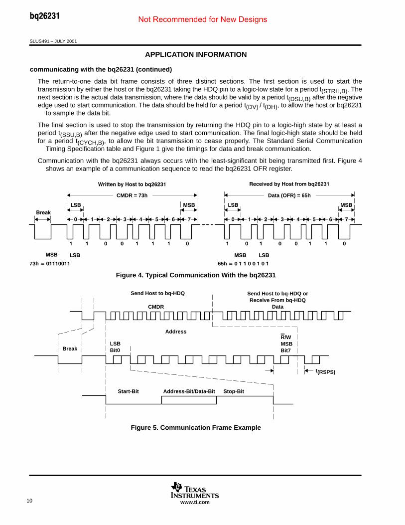
The return-to-one data bit frame consists of three distinct sections. The first section is used to start thetransmission by either the host or the bq26231 taking the HDQ pin to a logic-low state for a period t(STRH,B). Thenext section is the actual data transmission, where the data should be valid by a period t(DSU,B) after the negativeedge used to start communication. The data should be held for a period t(DV) / t(DH), to allow the host or bq26231
to sample the data bit.
The final section is used to stop the transmission by returning the HDQ pin to a logic-high state by at least aperiod t(SSU,B) after the negative edge used to start communication. The final logic-high state should be heldfor a period t(CYCH,B), to allow the bit transmission to cease properly. The Standard Serial Communication
Timing Specification table and Figure 1 give the timings for data and break communication.
Communication with the bq26231 always occurs with the least-significant bit being transmitted first. Figure 4shows an example of a communication sequence to read the bq26231 OFR register.
!
"
# "
CMDR = 73h
# "
Data (OFR) = 65h
Figure 4. Typical Communication With the bq26231
Send Host to bq-HDQ
CMDR
Break
Start-Bit Address-Bit/Data-Bit Stop-Bit
LSBBit0
R/WMSBBit7
Send Host to bq-HDQ orReceive From bq-HDQ
Data
t(RSPS)
Address
Figure 5. Communication Frame Example
Not Recommended for New Designs

SLUS491 – JULY 2001
11www.ti.com
APPLICATION INFORMATION
bq26231 command and status registers
The bq26231 command and status registers are listed and described in Table 4.
command (CMDR)
The write-only command register is accessed when the bq26231 has received eight contiguous valid commandbits. The command register contains two fields:
W/R
Command address
The W/R bit of the command register is used to select whether the received command is for a read or a writefunction. The W/R values are:
CDMR BITS
7 6 5 4 3 2 1 0
W/R – – – – – – –
where W/R is
0 The bq26231 outputs the requested register contents specified by the address portion of the CMDR.
1 The following eight bits should be written to the register specified by the address portion of the CMDR.
Table 4. bq26231 Command and Status Registers
Symbol Register NameHDQ
Address(hex)
Read/Write
Bit 7(MSB) Bit 6 Bit 5 Bit 4 Bit 3 Bit 2 Bit 1
Bit0(LSB)
CMDR Command register – Write W/R AD6 AD5 AD4 AD3 AD2 AD1 AD0
DCRHDischarge countregister high byte 7F Read DCRH7 DCRH6 DCRH5 DCRH4 DCRH3 DCRH2 DCRH1 DCRH0
DCRLDischarge countregister low byte 7E Read DCRL7 DCRL6 DCRL5 DCRL4 DCRL3 DCRL2 DCRL1 DCRL0
CCRHCharge countregister high byte 7D Read CCRH7 CCRH6 CCRH5 CCRH4 CCRH3 CCRH2 CCRH1 CCRH0
CCRLCharge countregister low byte 7C Read CCRL7 CCRL6 CCRL5 CCRL4 CCRL3 CCRL2 CCRL1 CCRL0
SCRHSelf-discharge countregister high byte 7B Read SCRH7 SCRH6 SCRH5 SCRH4 SCRH3 SCRH2 SCRH1 SCRH0
SCRLSelf-discharge countregister low byte 7A Read SCRL7 SCRL6 SCRL5 SCRL4 SCRL3 SCRL2 SCRL1 SCRL0
DTCHDischarge timecount high byte 79 Read DTCH7 DTCH6 DTCH5 DTCH4 DTCH3 DTCH2 DTCH1 DTCH0
DTCLDischarge timecount low byte 78 Read DTCL7 DTCL6 DTCL5 DTCL4 DTCL3 DTCL2 DTCL1 DTCL0
CTCHCharge time counthigh byte 77 Read CTCH7 CTCH6 CTCH5 CTCH4 CTCH3 CTCH2 CTCH1 CTCH0
CTCLCharge time countlow byte 76 Read CTCL7 CTCL6 CTCL5 CTCL4 CTCL3 CTCL2 CTCL1 CTCL0
MODE/WOE Mode/WOE register 75
Read/Write OVERDQ CAL STC STD WOE3 WOE2 WOE1 0
TMP/CLR
Temperature/clearregister 74
Read/Write TMP2 TMP1 TMP0 CTC DTC SCR CCR DCR
OFR Offset register 73Read/Write OFR7 OFR6 OFR5 OFR4 OFR3 OFR2 OFR1 OFR0
Not Recommended for New Designs

SLUS491 – JULY 2001
12 www.ti.com
APPLICATION INFORMATION
command (CMDR) (continued)
The lower seven-bit field of CMDR contains the address portion of the register to be accessed.
CDMR BITS
7 6 5 4 3 2 1 0
– AD6 AD5 AD4 AD3 AD2 AD1 AD0
discharge count registers (DCRH/DCRL)
The DCRH high-byte register (address = 7F hex) and the DCRL low-byte register (address = 7E hex) containthe count of the discharge and are incremented whenever V(SR1) < V(SR2). These registers continue to countbeyond FFFF hex, so proper register maintenance should be done by the host system. The TMP/CLR register
is used to force the reset of both the DCRH and DCRL to zero.
charge count registers (CCRH/CCRL)
The CCRH high-byte register (address = 7D hex) and the CCRL low-byte register (address = 7C hex) containthe count of the charge, and are incremented whenever V(SR1) > V(SR2). These registers continue to countbeyond FFFF hex, so proper register maintenance should be done by the host system. The TMP/CLR register
is used to force the reset of both the CCRH and CCRL to zero.
self-discharge count registers (SCRH/SCRL)
The SCRH high-byte register (address = 7B hex) and the SCRL low-byte register (address = 7A hex) containthe self-discharge count. These registers are continually updated when the bq26231 is in its normal operatingmode. The counts in these registers are incremented based on time and temperature. The SCR counts at a rateof 1 count per hour at 20–30°C and doubles every 10°C to greater than 60°C (16 counts/hour). The count willhalve every 10°C below 20–30°C to less than 0°C (1 count/8 hours). These registers continue to count beyondFFFF hex, so proper register maintenance should be done by the host system. The TMP/CLR register is used
to force the reset of both the SCRH and SCRL to zero.
discharge time count registers (DTCH/DTCL)
The DTCH high-byte register (address = 79 hex) and the DTCL low-byte register (address = 78 hex) are usedto determine the length of time the V(SR1) < V(SR2), indicating a discharge. The counts in these registers areincremented at a rate of 4096 counts per hour. If the DTCH/DTCL register continues to count beyond FFFF hex,the STD bit is set in the MODE/WOE register, indicating a rollover. Once set, DTCH and DTCL increment at arate of 16 counts per hour. The TMP/CLR register is used to force the reset of both the DTCH and DTCL to zero.
NOTE:If a second rollover occurs, STD is cleared. Access to the bq26231 should be timed to clear
DTCH/DTCL more often than every 170 days.
charge time count registers (CTCH/CTCL)
The CTCH high-byte register (address = 77 hex) and the CTCL low-byte register (address = 76 hex) are usedto determine the length of time the V(SR1) > V(SR2), indicating a charge. The counts in these registers areincremented at a rate of 4096 counts per hour. If the CTCH/CTCL registers continue to count beyond FFFF hex,the STC bit is set in the MODE/WOE register, indicating a rollover. Once set, DTCH and DTCL increment at arate of 16 counts per hour. The TMP/CLR register is used to force the reset of both the CTCH and CTCL to zero.
NOTE:If a second rollover occurs, STD is cleared. Access to the bq26231 should be timed to clear
CTCH/CTCL more often than every 170 days.
Not Recommended for New Designs

SLUS491 – JULY 2001
13www.ti.com
APPLICATION INFORMATION
mode/wake-up enable register
The Mode/WOE register (address = 75 hex) contains the calibration and wake-up enable information, and theSTC and STD bits as described below.
The override DQ (OVRDQ) bit (bit 7) is used to override the requirement for HDQ to be low before initiating V(OS)calibration. This bit is normally set to zero. If OVRDQ is written to one, the bq26231 begins offset calibration
when |V(SR)| < V(WOE) where HDQ = Don’t care.
The OVRDQ location is
MODE/WOE BITS
7 6 5 4 3 2 1 0
OVERDQ – – – – – – –
where OVRDQ is
0 HDQ = 0 and |V(SR)| < V(WOE) for V(OS) calibration to begin
1 HDQ = Don’t care and |V(SR)| < V(WOE) for V(OS) calibration to begin
NOTE:The OVRDQ bit should only be used in conjunction with a calibration cycle. Normal operation ofthe bq26231 is not ensured when this bit is set. After a valid calibration cycle, bit 7 is reset to zero.
The calibration (CAL) bit 6 is used to enable the bq26231 offset calibration test. Setting this bit to 1 enables aV(OS) calibration whenever HDQ is low (default), and |V(SR)| < V(WOE). This bit is cleared to 0 by the bq26231whenever a valid V(OS) calibration is completed, and the OFR register is updated with the new calculated offset.
The bit remains 1 if the offset calibration was not completed.
The CAL location is
MODE/WOE BITS
7 6 5 4 3 2 1 0
– CAL – – – – – –
where CAL is
0 Valid offset calibration
1 Offset calibration pending
The slow time charge (STC) and slow time discharge (STD) flags indicate if the CTC or DTC registers have rolledover beyond FFFF hex. STC set to 1 indicates a CTC rollover; STD set to 1 indicates a DTC rollover.
The STC and STD locations are
MODE/WOE BITS
7 6 5 4 3 2 1 0
– – STC STD – – – –
where STC/STD is
0 No rollover
1 Rollover occurred in the corresponding CTC/DTC register.
The WOE bits (bits 3–1) are used in conjunction with the CAL bit for the calibration process. When the CAL bitis set to 1, the bq26231 enables a V(OS) calibration whenever HDQ is low (default), and |V(SR)| < V(WOE). Onbq26231 initialization (power-on reset) the WOE bits are set to1. Setting all of these bits to zero is not valid. Refer
to Table 5 for the various WOE values.
Not Recommended for New Designs

SLUS491 – JULY 2001
14 www.ti.com
APPLICATION INFORMATION
mode/wake-up enable register (continued)
The WOE 3–1 locations are
MODE/WOE BITS
7 6 5 4 3 2 1 0
– – – – WOE3 WOE2 WOE1 –
where WOE3–1 is determined by dividing 3.84 mV by the value in WOE.
NOTE:Bit 0 of the MODE/WOE register is reserved and must remain 0.
Table 5. WOE Thresholds
WOE3–1 (hex) V(WOE) (mV)0 N/A
1 3.840
2 1.920
3 1.280
4 0.960
5 0.768
6 0.640
7 (default after POR) 0.549
temperature and clear register
The TMP/CLR register (address = 74 hex) is used to give the present temperature step between < 0°C and> 60°C and clear the various count registers. The values of the TMP0–TMP2 (bits 5–7) denote the currenttemperature step sense by the bq26231 as outlined in Table 3. The bq26231 temperature sense is trimmedto ±2°C typical (±4°C maximum).
The TMP2–0 locations are
TMP/CLR BITS
7 6 5 4 3 2 1 0
TMP2 TMP1 TMP0 – – – – –
where TMP2–0 is the temperature step sensed by this bq26231.
The Clear bits (Bits 0–4) are used to reset the various bq26231 counters and STC and STD bits to zero. Writingthe bits to 1 resets the corresponding register to 0. The clear bit resets to 0, indicating a successful register reset.Each clear bit is independent, so it is possible to clear the DCRH/DCRL registers without affecting the valuesin any other bq26231 register. The high-byte and low-byte registers are both cleared when the corresponding
bit is written to 1.
Not Recommended for New Designs

SLUS491 – JULY 2001
15www.ti.com
APPLICATION INFORMATION
temperature and clear register (continued)
The clear bit locations are
TMP/CLR BITS
7 6 5 4 3 2 1 0
– – – CTC DTC SCR CCR DCR
Where:
The CTC bit (bit 4) resets both the CTCH and CTCL registers and the STC bit to 0.The DTC bit (bit 3) resets both the DTCH and DTCL registers and the STD bit to 0.The SCR bit (bit 2) resets both the SCRH and SCRL registers to 0.The CCR bit (bit 1) resets both the CCRH and CCRL registers to 0.The DCR bit (bit 0) resets both the DCRH and DCRL registers to 0.
offset register (OFR)
The OFR register (address = 73 hex) is used to store the calculated V(OS) of the bq26231. The OFR value canbe used to cancel the voltage offset between V(SR1) and V(SR2). The up/down offset counter is centered at zero.
The actual offset is an 8-bit 2s complement value located in OFR.
The OFR locations are
TMP/CLR BITS
7 6 5 4 3 2 1 0
OFR7 OFR6 OFR5 OFR4 OFR3 OFR2 OFR1 OFR0
where OFR7 is
0 Discharge
1 Charge
Not Recommended for New Designs

PACKAGE OPTION ADDENDUM
www.ti.com 24-Aug-2018
Addendum-Page 1
PACKAGING INFORMATION
Orderable Device Status(1)
Package Type PackageDrawing
Pins PackageQty
Eco Plan(2)
Lead/Ball Finish(6)
MSL Peak Temp(3)
Op Temp (°C) Device Marking(4/5)
Samples
BQ26231PW NRND TSSOP PW 8 150 Green (RoHS& no Sb/Br)
CU NIPDAU Level-2-260C-1 YEAR -20 to 70 26231
BQ26231PWR NRND TSSOP PW 8 2000 Green (RoHS& no Sb/Br)
CU NIPDAU Level-2-260C-1 YEAR -20 to 70 26231
BQ26231PWRG4 NRND TSSOP PW 8 2000 Green (RoHS& no Sb/Br)
CU NIPDAU Level-2-260C-1 YEAR -20 to 70 26231
(1) The marketing status values are defined as follows:ACTIVE: Product device recommended for new designs.LIFEBUY: TI has announced that the device will be discontinued, and a lifetime-buy period is in effect.NRND: Not recommended for new designs. Device is in production to support existing customers, but TI does not recommend using this part in a new design.PREVIEW: Device has been announced but is not in production. Samples may or may not be available.OBSOLETE: TI has discontinued the production of the device.
(2) RoHS: TI defines "RoHS" to mean semiconductor products that are compliant with the current EU RoHS requirements for all 10 RoHS substances, including the requirement that RoHS substancedo not exceed 0.1% by weight in homogeneous materials. Where designed to be soldered at high temperatures, "RoHS" products are suitable for use in specified lead-free processes. TI mayreference these types of products as "Pb-Free".RoHS Exempt: TI defines "RoHS Exempt" to mean products that contain lead but are compliant with EU RoHS pursuant to a specific EU RoHS exemption.Green: TI defines "Green" to mean the content of Chlorine (Cl) and Bromine (Br) based flame retardants meet JS709B low halogen requirements of <=1000ppm threshold. Antimony trioxide basedflame retardants must also meet the <=1000ppm threshold requirement.
(3) MSL, Peak Temp. - The Moisture Sensitivity Level rating according to the JEDEC industry standard classifications, and peak solder temperature.
(4) There may be additional marking, which relates to the logo, the lot trace code information, or the environmental category on the device.
(5) Multiple Device Markings will be inside parentheses. Only one Device Marking contained in parentheses and separated by a "~" will appear on a device. If a line is indented then it is a continuationof the previous line and the two combined represent the entire Device Marking for that device.
(6) Lead/Ball Finish - Orderable Devices may have multiple material finish options. Finish options are separated by a vertical ruled line. Lead/Ball Finish values may wrap to two lines if the finishvalue exceeds the maximum column width.
Important Information and Disclaimer:The information provided on this page represents TI's knowledge and belief as of the date that it is provided. TI bases its knowledge and belief on informationprovided by third parties, and makes no representation or warranty as to the accuracy of such information. Efforts are underway to better integrate information from third parties. TI has taken andcontinues to take reasonable steps to provide representative and accurate information but may not have conducted destructive testing or chemical analysis on incoming materials and chemicals.TI and TI suppliers consider certain information to be proprietary, and thus CAS numbers and other limited information may not be available for release.

PACKAGE OPTION ADDENDUM
www.ti.com 24-Aug-2018
Addendum-Page 2
In no event shall TI's liability arising out of such information exceed the total purchase price of the TI part(s) at issue in this document sold by TI to Customer on an annual basis.

TAPE AND REEL INFORMATION
*All dimensions are nominal
Device PackageType
PackageDrawing
Pins SPQ ReelDiameter
(mm)
ReelWidth
W1 (mm)
A0(mm)
B0(mm)
K0(mm)
P1(mm)
W(mm)
Pin1Quadrant
BQ26231PWR TSSOP PW 8 2000 330.0 12.4 7.0 3.6 1.6 8.0 12.0 Q1
PACKAGE MATERIALS INFORMATION
www.ti.com 11-Jun-2013
Pack Materials-Page 1

*All dimensions are nominal
Device Package Type Package Drawing Pins SPQ Length (mm) Width (mm) Height (mm)
BQ26231PWR TSSOP PW 8 2000 367.0 367.0 35.0
PACKAGE MATERIALS INFORMATION
www.ti.com 11-Jun-2013
Pack Materials-Page 2

www.ti.com
PACKAGE OUTLINE
C
TYP6.66.2
1.2 MAX
6X 0.65
8X 0.300.19
2X1.95
0.150.05
(0.15) TYP
0 - 8
0.25GAGE PLANE
0.750.50
A
NOTE 3
3.12.9
BNOTE 4
4.54.3
4221848/A 02/2015
TSSOP - 1.2 mm max heightPW0008ASMALL OUTLINE PACKAGE
NOTES: 1. All linear dimensions are in millimeters. Any dimensions in parenthesis are for reference only. Dimensioning and tolerancing per ASME Y14.5M. 2. This drawing is subject to change without notice. 3. This dimension does not include mold flash, protrusions, or gate burrs. Mold flash, protrusions, or gate burrs shall not exceed 0.15 mm per side. 4. This dimension does not include interlead flash. Interlead flash shall not exceed 0.25 mm per side.5. Reference JEDEC registration MO-153, variation AA.
18
0.1 C A B
54
PIN 1 IDAREA
SEATING PLANE
0.1 C
SEE DETAIL A
DETAIL ATYPICAL
SCALE 2.800

www.ti.com
EXAMPLE BOARD LAYOUT
(5.8)
0.05 MAXALL AROUND
0.05 MINALL AROUND
8X (1.5)8X (0.45)
6X (0.65)
(R )TYP
0.05
4221848/A 02/2015
TSSOP - 1.2 mm max heightPW0008ASMALL OUTLINE PACKAGE
SYMM
SYMM
LAND PATTERN EXAMPLESCALE:10X
1
45
8
NOTES: (continued) 6. Publication IPC-7351 may have alternate designs. 7. Solder mask tolerances between and around signal pads can vary based on board fabrication site.
METALSOLDER MASKOPENING
NON SOLDER MASKDEFINED
SOLDER MASK DETAILSNOT TO SCALE
SOLDER MASKOPENING
METAL UNDERSOLDER MASK
SOLDER MASKDEFINED

www.ti.com
EXAMPLE STENCIL DESIGN
(5.8)
6X (0.65)
8X (0.45)8X (1.5)
(R ) TYP0.05
4221848/A 02/2015
TSSOP - 1.2 mm max heightPW0008ASMALL OUTLINE PACKAGE
NOTES: (continued) 8. Laser cutting apertures with trapezoidal walls and rounded corners may offer better paste release. IPC-7525 may have alternate design recommendations. 9. Board assembly site may have different recommendations for stencil design.
SYMM
SYMM
1
45
8
SOLDER PASTE EXAMPLEBASED ON 0.125 mm THICK STENCIL
SCALE:10X

IMPORTANT NOTICE
Texas Instruments Incorporated (TI) reserves the right to make corrections, enhancements, improvements and other changes to itssemiconductor products and services per JESD46, latest issue, and to discontinue any product or service per JESD48, latest issue. Buyersshould obtain the latest relevant information before placing orders and should verify that such information is current and complete.TI’s published terms of sale for semiconductor products (http://www.ti.com/sc/docs/stdterms.htm) apply to the sale of packaged integratedcircuit products that TI has qualified and released to market. Additional terms may apply to the use or sale of other types of TI products andservices.Reproduction of significant portions of TI information in TI data sheets is permissible only if reproduction is without alteration and isaccompanied by all associated warranties, conditions, limitations, and notices. TI is not responsible or liable for such reproduceddocumentation. Information of third parties may be subject to additional restrictions. Resale of TI products or services with statementsdifferent from or beyond the parameters stated by TI for that product or service voids all express and any implied warranties for theassociated TI product or service and is an unfair and deceptive business practice. TI is not responsible or liable for any such statements.Buyers and others who are developing systems that incorporate TI products (collectively, “Designers”) understand and agree that Designersremain responsible for using their independent analysis, evaluation and judgment in designing their applications and that Designers havefull and exclusive responsibility to assure the safety of Designers' applications and compliance of their applications (and of all TI productsused in or for Designers’ applications) with all applicable regulations, laws and other applicable requirements. Designer represents that, withrespect to their applications, Designer has all the necessary expertise to create and implement safeguards that (1) anticipate dangerousconsequences of failures, (2) monitor failures and their consequences, and (3) lessen the likelihood of failures that might cause harm andtake appropriate actions. Designer agrees that prior to using or distributing any applications that include TI products, Designer willthoroughly test such applications and the functionality of such TI products as used in such applications.TI’s provision of technical, application or other design advice, quality characterization, reliability data or other services or information,including, but not limited to, reference designs and materials relating to evaluation modules, (collectively, “TI Resources”) are intended toassist designers who are developing applications that incorporate TI products; by downloading, accessing or using TI Resources in anyway, Designer (individually or, if Designer is acting on behalf of a company, Designer’s company) agrees to use any particular TI Resourcesolely for this purpose and subject to the terms of this Notice.TI’s provision of TI Resources does not expand or otherwise alter TI’s applicable published warranties or warranty disclaimers for TIproducts, and no additional obligations or liabilities arise from TI providing such TI Resources. TI reserves the right to make corrections,enhancements, improvements and other changes to its TI Resources. TI has not conducted any testing other than that specificallydescribed in the published documentation for a particular TI Resource.Designer is authorized to use, copy and modify any individual TI Resource only in connection with the development of applications thatinclude the TI product(s) identified in such TI Resource. NO OTHER LICENSE, EXPRESS OR IMPLIED, BY ESTOPPEL OR OTHERWISETO ANY OTHER TI INTELLECTUAL PROPERTY RIGHT, AND NO LICENSE TO ANY TECHNOLOGY OR INTELLECTUAL PROPERTYRIGHT OF TI OR ANY THIRD PARTY IS GRANTED HEREIN, including but not limited to any patent right, copyright, mask work right, orother intellectual property right relating to any combination, machine, or process in which TI products or services are used. Informationregarding or referencing third-party products or services does not constitute a license to use such products or services, or a warranty orendorsement thereof. Use of TI Resources may require a license from a third party under the patents or other intellectual property of thethird party, or a license from TI under the patents or other intellectual property of TI.TI RESOURCES ARE PROVIDED “AS IS” AND WITH ALL FAULTS. TI DISCLAIMS ALL OTHER WARRANTIES ORREPRESENTATIONS, EXPRESS OR IMPLIED, REGARDING RESOURCES OR USE THEREOF, INCLUDING BUT NOT LIMITED TOACCURACY OR COMPLETENESS, TITLE, ANY EPIDEMIC FAILURE WARRANTY AND ANY IMPLIED WARRANTIES OFMERCHANTABILITY, FITNESS FOR A PARTICULAR PURPOSE, AND NON-INFRINGEMENT OF ANY THIRD PARTY INTELLECTUALPROPERTY RIGHTS. TI SHALL NOT BE LIABLE FOR AND SHALL NOT DEFEND OR INDEMNIFY DESIGNER AGAINST ANY CLAIM,INCLUDING BUT NOT LIMITED TO ANY INFRINGEMENT CLAIM THAT RELATES TO OR IS BASED ON ANY COMBINATION OFPRODUCTS EVEN IF DESCRIBED IN TI RESOURCES OR OTHERWISE. IN NO EVENT SHALL TI BE LIABLE FOR ANY ACTUAL,DIRECT, SPECIAL, COLLATERAL, INDIRECT, PUNITIVE, INCIDENTAL, CONSEQUENTIAL OR EXEMPLARY DAMAGES INCONNECTION WITH OR ARISING OUT OF TI RESOURCES OR USE THEREOF, AND REGARDLESS OF WHETHER TI HAS BEENADVISED OF THE POSSIBILITY OF SUCH DAMAGES.Unless TI has explicitly designated an individual product as meeting the requirements of a particular industry standard (e.g., ISO/TS 16949and ISO 26262), TI is not responsible for any failure to meet such industry standard requirements.Where TI specifically promotes products as facilitating functional safety or as compliant with industry functional safety standards, suchproducts are intended to help enable customers to design and create their own applications that meet applicable functional safety standardsand requirements. Using products in an application does not by itself establish any safety features in the application. Designers mustensure compliance with safety-related requirements and standards applicable to their applications. Designer may not use any TI products inlife-critical medical equipment unless authorized officers of the parties have executed a special contract specifically governing such use.Life-critical medical equipment is medical equipment where failure of such equipment would cause serious bodily injury or death (e.g., lifesupport, pacemakers, defibrillators, heart pumps, neurostimulators, and implantables). Such equipment includes, without limitation, allmedical devices identified by the U.S. Food and Drug Administration as Class III devices and equivalent classifications outside the U.S.TI may expressly designate certain products as completing a particular qualification (e.g., Q100, Military Grade, or Enhanced Product).Designers agree that it has the necessary expertise to select the product with the appropriate qualification designation for their applicationsand that proper product selection is at Designers’ own risk. Designers are solely responsible for compliance with all legal and regulatoryrequirements in connection with such selection.Designer will fully indemnify TI and its representatives against any damages, costs, losses, and/or liabilities arising out of Designer’s non-compliance with the terms and provisions of this Notice.
Mailing Address: Texas Instruments, Post Office Box 655303, Dallas, Texas 75265Copyright © 2018, Texas Instruments Incorporated