Embed Size (px)
Citation preview
11 AK-33
Service Manual
1. INTRODUCTION ________________________________________________4
2. SMALL SIGNAL PART WITH TDA8885 _____________________________42.1. Vision IF amplifier _________________________________________________ 4
2.2. Video Switches_____________________________________________________ 5
2.3. Sound Circuit______________________________________________________ 5
2.4. Synchronisation circuit ______________________________________________ 5
2.5. Chroma and Luminance processing ___________________________________ 6
2.6. Colour Decoder ____________________________________________________ 6
2.7. PICTURE IMPROVEMENT FEATURES______________________________ 7
2.8. RGB output circuit and black-current stabilisation_______________________ 7
2.9. EAST – WEST OUTPUT STAGE_____________________________________ 8
3. TUNER_________________________________________________________8
4. VIDEO SWITCH TEA6415C _______________________________________9
5. MULTI STANDARD SOUND PROCESSOR___________________________9
6. SOUND OUTPUT STAGE WITH TDA 7265___________________________9
7. VERTICAL OUTPUT STAGE WITH STV 9379 _______________________10
8. VIDEO OUTPUT AMPLIFIER TDA6108 ____________________________10
9. COMBFILTER TDA 9181_________________________________________10
10. POWER SUPPLY (SMPS) _______________________________________10
11. POWER FACTOR CORRECTION ________________________________10
12. MICROCONTROLLER SDA555X ________________________________1012.1. General Features ________________________________________________ 10
12.2. External Crystal and Programmable clock speed______________________ 10
12.3. Microcontroller Features _________________________________________ 10
12.4. Memory _______________________________________________________ 11
12.5. Display Features ________________________________________________ 11
12.6. ROM Characters ________________________________________________ 11
12.7. Acquisition Features _____________________________________________ 11
12.8. Ports __________________________________________________________ 11
13. SERIAL ACCESS CMOS 8K (1024*8) EEPROM ST24C08 ____________12
14. CLASS AB STEREO HEADPHONE DRIVER TDA1308 ______________12
15. SAW FILTERS ________________________________________________12
16. IC DESCRIPTIONS AND INTERNAL BLOCK DIAGRAM____________1216.1. TDA8885: ______________________________________________________ 12
16.1.1. GENERAL DESCRIPTION _____________________________________________1216.1.2. FEATURES__________________________________________________________1216.1.3. Pin Description _______________________________________________________13
16.2. UV1315, UV1316 ________________________________________________ 1516.2.1. General description of UV1315: __________________________________________1516.2.2. Features of UV1315: ___________________________________________________1516.2.3. General description of UV1316: __________________________________________1516.2.4. Features of UV1316: ___________________________________________________15
16.3. TEA6415C:_____________________________________________________ 1616.3.1. General Description: ___________________________________________________1616.3.2. Features: ____________________________________________________________16
16.4. TDA7265: ______________________________________________________ 1716.4.1. Features: ____________________________________________________________1716.4.2. Pinning: _____________________________________________________________17
16.5. TDA6108Q: ____________________________________________________ 1716.5.1. Features: ____________________________________________________________17
16.6. 74 HCT 32 _____________________________________________________ 1816.6.1. PINNING ___________________________________________________________18
16.7. MC44608 ______________________________________________________ 1816.7.1. General description:____________________________________________________1816.7.2. General Features ______________________________________________________18
16.8. SDA5555: ______________________________________________________ 1916.8.1. General description:____________________________________________________19
16.9. TDA9181: ______________________________________________________ 2016.9.1. General Features:______________________________________________________2016.9.2. Limits: ______________________________________________________________20
16.10. TCD1102: ______________________________________________________ 2116.10.1. Description ________________________________________________________2116.10.2. Applications _______________________________________________________2116.10.3. General features: ____________________________________________________21
16.11. ST24C08: ______________________________________________________ 2116.11.1. General description:__________________________________________________2116.11.2. Features: __________________________________________________________21
16.12. TDA1308: ______________________________________________________ 2216.12.1. Features: __________________________________________________________22
16.13. PCF8583: ______________________________________________________ 2216.13.1. FEATURES________________________________________________________2216.13.2. GENERAL DESCRIPTION ___________________________________________23
16.14. MC33260: ______________________________________________________ 2316.14.1. General Features:____________________________________________________2316.14.2. Safety Features: _____________________________________________________2316.14.3. LIMITS:___________________________________________________________2316.14.4. PINNING _________________________________________________________23
16.15. STV9379: ______________________________________________________ 2416.15.1. DESCRIPTION_____________________________________________________2416.15.2. PINNING _________________________________________________________24
16.16. MSP34XX :_____________________________________________________ 24
MSP3410D ________________________________________________________2416.17. LM358N: ______________________________________________________ 26
16.17.1. General Description__________________________________________________2616.17.2. Unique Characteristics________________________________________________2616.17.3. Advantages ________________________________________________________2616.17.4. Features ___________________________________________________________26
17. AK33 CHASSIS MANUAL ADJUSTMENTS PROCEDURE ___________26
1. INTRODUCTION11AK33 is a 110ø chassis capable of driving 28-29”,32”,33” tubes at appropriate currents The chassis is aFrequency Controlled Tuning (PLL) and control system for multi-standard TV receivers with on-screen-display (OSD) for all relevant control functions. The system is based on the ‘one-chip’ I2C buscontrolled video processing / deflection IC TDA8885 which also controls sound.German stereo and Nicam is detected and processed by the MSP 3410 G. Dolby sound is processed byMSP 3452 G, virtual dolby by MSP 3411G, BTSC Stereo by MSP 3430G IC’s by option. All soundprocessors also control the sound volume, balance, tone and spatial stereo effect.The user-interface is menu based control system with cursor keys. Only for some functions the colourkeys are needed: This means that some of the functions can also be operated from the local keyboard(i.e. Vol -, Vol +, P -, P+ and M).Teletext is done by the microcontroller on-chip teletext module.
2. SMALL SIGNAL PART WITH TDA8885The TDA8885 combine all small signal functions required for a colour TV receiver.
2.1. Vision IF amplifierThe IF-amplifier contains 3 ac-coupled control stages with a total gain control range, which is higherthen 66 dB. The sensitivity of the circuit is comparable. The video signal is demodulated by means ofan alignment-free PLL carrier regenerator with an internal VCO. This VCO is calibrated by means of adigital control circuit, which uses the clock frequency of the m-Controller/Teletext decoder as areference. The frequency setting for the various standards (33.4, 33.9, 38, 38.9, 45.75 and 58.75 MHz)is realised via the I 2 C-bus. To get a good performance for phase modulated carrier signals the controlspeed of the PLL can be increased by means of the FFI bit. The AFC output is generated by the digitalcontrol circuit of the IF-PLL demodulator and can be read via the I 2 C bus. For fast search tuningsystems the window of the AFC can be increased with a factor 3. The setting is realised with the AFWbit. The AGC-detector operates on top sync and top white-level. The demodulation polarity is switchedvia the I 2 C-bus. The AGC detector capacitor is integrated. The time-constant can be chosen via the I 2C-bus. The time-constant of the AGC system during positive modulation is rather long to avoid visiblevariations of the signal amplitude. To improve the speed of the AGC system a circuit has been includedwhich detects whether the AGC detector is activated every frame period. When during 3 field periodsno action is detected the speed of the system is increased. For signals without peak white information
the system switches automatically to a gated black level AGC. Because a black level clamp pulse isrequired for this way of operation the circuit will only switch to black level AGC in the internal mode.The circuit contains a video identification circuit, which is independent of the synchronisation circuit.Therefore search tuning is possible when the display section of the receiver is used as a monitor.However, this Ident circuit cannot be made as sensitive as the slower sync Ident circuit (SL) and we useboth Ident outputs to obtain a reliable search system. The Ident output is supplied to the tuning systemvia the I 2 C-bus. The input of the identification circuit is connected to pin 24, the internal CVBS input.This has the advantage that the Ident circuit can also be made operative when a scrambled signal isreceived (descrambler connected between the IF video output (pin 16) and pin 24). A second advantageis that the Ident circuit can be used when the IF amplifier is not used The video Ident circuit can also beused to identify the selected CBVS or Y/C signal. The switching between the 2 modes can be realisedwith the VIM bit. The IC contains a group delay correction circuit, which can be switched between theBG and a flat group delay response characteristic. This has the advantage that in multi-standardreceivers no compromise has to be made for the choice of the SAW filter. Also the sound trap isintegrated within the IC .The centre frequency of the trap can be switched via the I 2 C-bus. For mono-FM versions it is possible to obtain a demodulated IF video signal which has not passed the sound trapso that an external stereo decoder can be driven. This function is selected by means of the ICO bit (sub-address 28H). The signal is available on pin 27 (audio output pin when ICO = 0). The S/N ratio of theselected video signal can be read via the bits SN1/SN0 in sub-address 03H.
2.2. Video SwitchesThe circuit has an input for the internal CVBS signal and 2 inputs for external CVBS or Y signals. Thecircuit has only 1 chroma input so that it is not possible to apply 2 separate Y/C inputs. The switchconfiguration is given in Fig. A. The selection of the various sources is made via the I 2 C-bus. TheQFP-64 version has 2 independently switchable outputs. The CVBS1O output is identical to theselected signal that is supplied to the internal video processing circuit and can therefore be used assource signal for a teletext decoder. Both CVBS outputs have an amplitude of 2.0 VP-P . The CVBS2Ooutput can for instance be used as drive signal for a PIP decoder. If the Y/C-3 signal is selected for oneof the outputs the luminance and chrominance signals are added so that a CVBS signal is obtainedagain.
2.3. Sound CircuitThe sound IF amplifier is similar to the vision IF amplifier and has a gain control range of about 66 dB.The AGC circuit is related to the SIF carrier levels (average level of AM or FM carriers) and ensures aconstant signal amplitude of the AM demodulator and the QSS mixer. A multiplier realises the singlereference QSS mixer. In this multiplier the SIF signal is converted to the intercarrier frequency bymixing it with the regenerated picture carrier from the VCO. The mixer output signal is supplied to theoutput via a high-pass filter for attenuation of the residual video signals. With this system a highperformance hi-fi stereo sound processing can be achieved. To optimise the performance of thedemodulator the offset can be compensated by means of an I 2 C-bus setting. The AM sounddemodulator is realised by a multiplier. The modulated sound IF signal is multiplied in phase with thelimited SIF signal. The demodulator output signal is supplied to the output via a low-pass filter forattenuation of the carrier harmonics. The AM signal is supplied to the output (pin 27) via the volumecontrol. It is possible to get the AM output signal (not controlled on amplitude) on the QSS intercarrieroutput. The selection is made by means of the AM bit in sub-address 29H. Another possibility is thatpin 11 can be used as external audio input pin and pin 49 can be used as (non-controlled) AM outputpin. This can be realised by means of the setting the control bits CMB0 and CMB1 in sub-address 22H.
2.4. Synchronisation circuitThe sync separator is preceded by a controlled amplifier, which adjusts the sync pulse amplitude to afixed level. These pulses are fed to the slicing stage, which is operating at 50% of the amplitude. Theseparated sync pulses are fed to the first phase detector and to the coincidence detector. Thiscoincidence detector is used to detect whether the line oscillator is synchronised with the incomingsignal and can also be used for transmitter identification. This circuit can be made less sensitive bymeans of the STM bit. This mode can be used during search tuning to avoid that the tuning system willstop at very weak input signals. The first PLL has a very high statically steepness so that the phase ofthe picture is independent of the line frequency. The horizontal drive signal is generated by an internalVCO, which is running at a frequency of 25 MHz. This oscillator is stabilised to that frequency byusing the 12 MHz frequency of the crystal oscillator as a reference. The time-constant of the first loop
can be forced by the I 2 C-bus (fast or slow). If required the IC can select the time-constant dependingon the noise content of the incoming video signal. The horizontal output signal is generated by meansof a second loop, which compares the phase of the internal oscillator signal with the phase of theincoming flyback pulse. The time-constant of this loop is connected externally and can be used as inputfor a dynamic horizontal phase correction. To obtain a smooth switch-on and switch-off behaviour ofthe horizontal output stage the horizontal drive signal is switched-on and off via the soft-start/soft-stopprocedure. This function is realised by means of a variation of the TON of the horizontal drive pulse.When the soft-start procedure is completed the horizontal output is gated with the flyback pulse so thatthe horizontal output transistor cannot be switched-on during the flyback time. An additional functionof the IC is the ‘low-power start-up’ feature. For this function a supply voltage with a value between 3and 5 V must be available at the start-up pin (required current 5 mA typical). When all sub-addressbytes have been sent and the POR and XPR flags have been cleared, the horizontal output can beswitched-on via the STB-bit (sub-address 24H). In this condition the horizontal drive signal has thenominal TOFF and the TON grows gradually from zero to the nominal value as indicated in the soft-start behaviour. As soon as the 8 V supply is present the switch-on procedure (e.g. closing of thesecond loop) is continued. The presence of the 8 V supply voltage is indicated by the SUP bit in the I 2C-bus output byte 02. The circuit generates a vertical sync pulse. This pulse can be selected on pin 49via the bits CMB1 and CMB0. In the 100 Hz input processor versions the vertical sync pulse isavailable on pin 63 and the horizontal pulse on pin 56. Via the I C-bus adjustments can be made of thehorizontal and vertical geometry. The vertical sawtooth generator drives the vertical output drivecircuit, which has a differential output current. For the E-W drive a single ended current output isavailable. A special feature is the zoom function for both the horizontal and vertical deflection and thevertical scroll function. When the horizontal scan is reduced to display 4 : 3 pictures on a 16 : 9 picturetube an accurate video blanking can be switched on to obtain well-defined edges on the screen.Overvoltage conditions (X-ray protection) can be detected via the EHT tracking pin. When anovervoltage condition is detected the horizontal output drive signal will be switched-off via the slowstop procedure but it is also possible that the drive is not switched-off and that just a protectionindication is given in the I 2 C-bus output bytes. The choice is made via the input bit PRD. When PRD= 1 and an overvoltage is detected the drive is switched-off and the STB bit is set to 0. Switching on ofthe drive is only possible when the XPR flag is cleared. The IC has a second protection input on the j2filter capacitor pin. When this input is activated the drive signal is switched-off immediately andswitched-on again via the slow start procedure. For this reason this protection input can be used as‘flash protection’. The drive pulses for the vertical sawtooth generator is obtained from a verticalcountdown circuit. This countdown circuit has various windows depending on the incoming signal (50Hz or 60 Hz and standard or non-standard). The countdown circuit can be forced in various modes bymeans of the I 2 C-bus. During the insertion of RGB signals the maximum vertical frequency isincreased to 72 Hz so that the circuit can also synchronise on signals with a higher vertical frequencylike VGA. To obtain short switching times of the countdown circuit during a channel change thedivider can be forced in the search window by means of the NCIN bit. The vertical deflection can beset in the de-interlace mode via the I 2 C bus.
2.5. Chroma and Luminance processingThe circuit contains a chroma bandpass and trap circuit. The filters are realised by means of gyratorcircuits and they are automatically calibrated by comparing the tuning frequency with the referencefrequency of the decoder. The luminance delay line and the delay for the peaking circuit are alsorealised by means of gyrator circuits. The centre frequency of the chroma bandpass filter is switchablevia the I 2 C-bus so that the performance can be optimised for ‘front-end’ signals and external CVBSsignals. During SECAM reception the centre frequency of the chroma trap is reduced to get a bettersuppression of the SECAM carrier frequencies.
2.6. Colour DecoderThe colour decoder can decode PAL, NTSC and SECAM signals. The internal clock signals for thevarious colour standards are generated by means of an internal VCO, which uses the 12 MHz crystalfrequency as a reference. Under bad-signal conditions (e.g. VCR-playback in feature mode), it mayoccur that the colour killer is activated although the colour PLL is still in lock. When this killing actionis not wanted it is possible to overrule the colour killer by forcing the colour decoder to the requiredstandard and to activate the FCO-bit (Forced Colour On) in subaddress 21H. The IC contains an
Automatic Colour Limiting (ACL) circuit which is switchable via the I 2 C-bus and which preventsthat oversaturation occurs when signals with a high chroma-to-burst ratio are received. The ACL circuitis designed such that it only reduces the chroma signal and not the burst signal. This has the advantagethat the colour sensitivity is not affected by this function. The SECAM decoder contains an auto-calibrating PLL demodulator which has two references, viz: the divided 12 MHz reference frequencyof the crystal oscillator which is used to tune the PLL to the desired free-running frequency and thebandgap reference to obtain the correct absolute value of the output signal. The VCO of the PLL iscalibrated during each vertical blanking period, when the IC is in search or SECAM mode. Thereference frequency of the colour decoder is fed to the Fsc output (pin 49) and can be used to tune anexternal comb filter. The base-band delay line is integrated. The demodulated colour difference signalsare internally supplied to the delay line. The colour difference matrix switches automatically betweenPAL/SECAM and NTSC, however, it is also possible to fix the matrix in the PAL standard.
2.7. PICTURE IMPROVEMENT FEATURESIn the TDA 8885 series various picture improvement features have been integrated. These features are:-Video dependent coring in the peaking circuit. The coring can be activated only in the low-light partsof the screen. This effectively reduces noise while having maximum peaking in the bright parts of thepicture.-Colour Transient Improvement (CTI). This circuit improves the rise and fall times of the colourdifference signals. The function is realised by using delay cells with a length of 300 ns.-Black-stretch. This circuit corrects the black level for incoming video signals, which have a deviationbetween the black level and the blanking, level (back porch). The time constant for the black stretcheris realised internally-Blue-stretch. This circuit is intended to shift colour near ‘white’ with sufficient contrast valuestowards more blue to obtain a brighter impression of the picture-White-stretch. This function adapts the transfer characteristic of the luminance amplifier in a non-linear way dependent on the picture content. The system operates such that maximum stretching isobtained when signals with a low video level are received. For bright pictures the stretching is notactive.-Dynamic skin tone (flesh) control. This function is realised in the YUV domain by detecting thecolourss near to the skin tone. The correction angle can be controlled via the I2 C-bus.
2.8. RGB output circuit and black-current stabilisationThe ICs have a very flexible control circuit for RGB and YUV input signals, which has the followingfeatures:· Input which can be used for YUV or RGB input signals and as YUV interface. The selection of thevarious modes can be realised via the I2 C-bus. For the YUV input 2 different input signal conditionscan be chosen. It is also possible to connect the synchronisation circuit to the incoming Y input signal.This input signal can be controlled on saturation, contrast and brightness.· The RGB-1 input which is intended for OSD/text signals and which can be controlled on contrast andbrightness. By means of the IE1 bit the insertion blanking can be switched on or off. Via the IN1 bit itcan be read whether the insertion pin has a high level or not. It is also possible to convert the incomingRGB-1 signal to a YUV signal. The resulting signal is supplied to the YUV outputs.· The TDA 888X versions have an additional YUV or RGB input which can be controlled on contrast,saturation and brightness. The various input signal conditions are given. The insertion blanking of thisinput can be switched-off by means of the IE2 bit. Via the IN2 bit it can be read whether the insertionpin has a high level or not. The control circuit has a half tone input, which can be used to reduce thecontrast setting during mixed mode operation for teletext and OSD signals. The output signal hasamplitude of about 2 V black-to-white at nominal input signals and nominal settings of the controls. Toincrease the flexibility of the IC it is possible to insert OSD and/or teletext signals directly at the RGBoutputs. This insertion mode is controlled via the insertion input (pin 38). This blanking action at theRGB outputs has some delay, which must be compensated externally.To obtain an accurate biasing of the picture tube the ‘Continuous Cathode Calibration’ system has beenincluded in this IC. Via the I2 C-bus a black level offset can be made with respect to the level which isgenerated by the black current stabilisation system. In this way different colour temperatures can beobtained for the bright and the dark part of the picture.
The black current stabilisation system checks the output level of the 3 channels and indicates whetherthe black level of the highest output is in a certain window (WBC-bit) or below or above this window(HBC-bit). This indication can be read from the I2 C-bus and can be used for automatic adjustment ofthe Vg2 voltage during the production of the TV receiver.The control circuit contains a beam current limiting circuit and a peak white limiting circuit. The peakwhite level is adjustable via the I2 C-bus. To prevent that the peak white limiting circuit reacts on thehigh frequency content of the video signal a low-pass filter is inserted in front of the peak detector. Thecircuit also contains a soft-clipper, which prevents that the high frequency peaks in the output signalbecome too high. The difference between the peak white limiting level and the soft clipping level isadjustable via the I2 C-bus in a few steps.During switch-off of the TV receiver, the black current control circuit generates a fixed beam current.This current ensures that the picture tube capacitance is discharged. During the switch-off period thevertical deflection can be placed in an overseen position so that the discharge is not visible on thescreen.
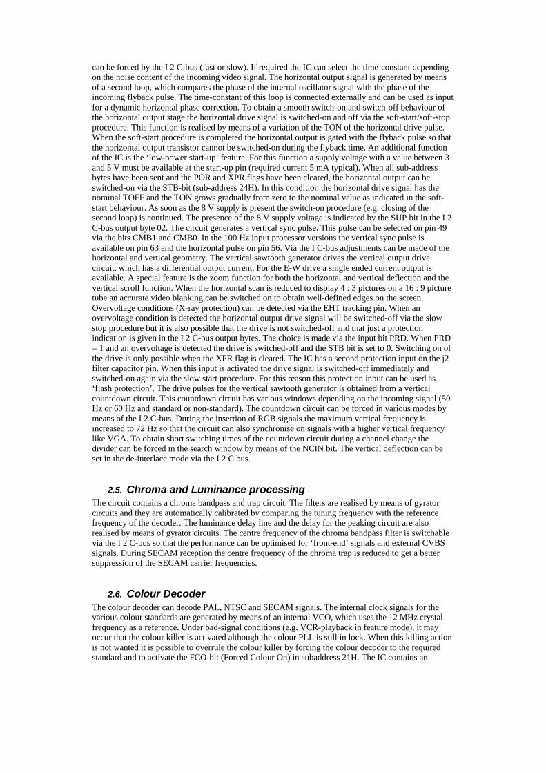
2.9. EAST – WEST OUTPUT STAGEIn order to obtain correct tracking of the vertical and horizontal EHT-correction, the EW output stageshould be dimensioned as illustrated in Figure. Resistor REW determines the gain of the EW outputstage. Resistor Rc determines the reference current for both the vertical sawtooth generator and thegeometry processor. The preferred value of Rc is 39 kW which results in a reference current of 100 mA(Vref = 3.9 V).The value of REW must be:
REW = RC * ( Vscan / (18* Vref ) )
Example: With Vref = 3.9 V; Rc =39 kohm and Vscan = 120 V then REW =68 kohm
3. TUNERPLL tuner is used as a tuner.UV1316 (VHF/UHF) is used as a PLL tuner. For only PALM/N, NTSC M applications UV 1336 are used as thePLL tuner.
Channel coverage of UV1316:
OFF-AIR CHANNELS CABLE CHANNELSBAND
CHANNELS FREQUENCY CHANNELSFREQUENCY
RANGE (MHz)RANGE (MHz)
Low Band E2 to C 48.25 to 82.25 (1) S01 to S0869.25 to 154.25
Mid Band E5 to E12 175.25 to 224.25 S09 to S38161.25 to 439.25
High Band E21 to E69 471.25 to 855.25 (2) S39 to S41447.25 to 463.25
(1). Enough margin is available to tune down to 45.25 MHz.(2). Enough margin is available to tune up to 863.25 MHz.
Noise Typical Max. Gain Min. TypicalMax.
Low band : 5dB 9dB All channels : 38dB 44dB52dB
Mid band : 5dB 9dB Gain Taper (of-air channels) : - -8dB
High band : 6dB 9dB
Channel Coverage UV1336:
BAND CHANNELS FREQUENCYRANGE (MHz)
Low Band 2 to D 55.25 to 139.25
Mid Band E to PP 145.25 to 391.25
High Band QQ to 69 397.25 to 801.25
Noise is typically 6dB for all channels. Gain is minimum 38dB and maximum 50dB for all channels.
4. VIDEO SWITCH TEA6415CIn case of three or more external sources are used, the video switch IC TEA6415C is used. The main function ofthis device is to switch 8 video-input sources on the 6 outputs.Each output can be switched on only one of each input. On each input an alignment of the lowest level of thesignal is made (bottom of sync. top for CVBS or black level for RGB signals).Each nominal gain between any input and output is 6.5dB.For D2MAC or Chroma signal the alignment isswitched off by forcing, with an external resistor bridge, 5VDC on the input. Each input can be used as a normalinput or as a MAC or Chroma input (with external Resistor Bridge). All the switching possibilities are changedthrough the BUS.Driving 75ohm load needs an external resistor.It is possible to have the same input connected to several outputs.
5. MULTI STANDARD SOUND PROCESSOR
The MSP 34x0D is designed to perform demodulation of FM or AM-Mono TV sound. Alternatively, two-carrierFM systems according to the German or Korean terrestrial specs or the satellite specs can be processed with theMSP 34x0D. Digital demodulation and decoding of NICAM-coded TV stereo sound, is done only by the MSP3410. The MSP 34x0D offers a powerful feature to calculate the carrier field strength which can be used forautomatic standard detection (terrestrial) and search algorithms (satellite).
6. SOUND OUTPUT STAGE WITH TDA 7265
TDA7265 is a class AB dual Audio power amplifier assembled in the multiwatt package.Mute stand-by function of the audio amplifier can be described as the following; the pin 5(MUTE/STAND-BY) controls the amplifier status by two different thresholds, referred to +Vs. WhenVpin (5) higher than (+Vs - 2.5V) the amplifier is in Stand-by mode and the final stage generators areoff. When Vpin (5) is between (+Vs – 2.5V) and (+Vs – 6V) the final stage current generators areswitched on and the amplifier is in mute mode. When the Vpin (5) is lower than +Vs – 6V the amplifieris play mode.
7. VERTICAL OUTPUT STAGE WITH STV 9379The IC TDA9379FA is the vertical deflection booster circuit. Two supply voltages, +12V and –12V areneeded to scan the inputs VERT+ and VERT-, respectively. And a third supply voltage, +45V for theflyback limiting are needed. The vertical deflection coil is connected in series between the output andfeedback to the input.
8. VIDEO OUTPUT AMPLIFIER TDA6108
The TDA6107/08Q includes three video output amplifiers in a SIL 9 MP (Single in Line 9 pins Medium Power)package SOT111BE, using high-voltage DMOS technology, and is intended to drive the three cathodes of a colourpicture tube.In contrast to previous types of DMOS video amplifiers, all external resistors (Rf, Ri and Ra) are integrated, so thegain is fixed.To obtain maximum performance, the amplifier should be used with black-current control and mounted on theCRT panel.
9. COMBFILTER TDA 9181The TDA 9181 is an adaptive PAL/NTSC comb filter with two internal delay lines, filters, clockcontrol, and input clamps. Video standards PAL B, G, H, I, M and N NTSC M are supported.Two CVBS input signals can be selected by means of input switch.In addition to the comb filter the circuit contains an output switch so that a selection can be made between thecombed CVBS signal and an external Y/C signal.The supply voltage is 5V.
10. POWER SUPPLY (SMPS)The DC voltages required at various parts of the chassis are provided by an SMPS transformer controlled by the ICMC44608, which is designed for driving, controlling and protecting switching transistor of SMPS. The transformerproduces 150V for FBT input, ? 14V for audio output IC, S+3.3, S+5V and 8V for TDA8885.
11. POWER FACTOR CORRECTIONThe MC33260 is a controller for Power Factor Correction pre-converters meeting internationalstandard requirements in electronic ballast and off–line power conversion applications. Designed todrive a free frequency discontinuous mode, it can also be synchronised and in any case, it features veryeffective protections that ensure a safe and reliable operation.
12. MICROCONTROLLER SDA555X
12.1. General Features• Feature selection via special function register• Simultaneous reception of TTX, VPS, PDC, and WSS (line 23)• Supply Voltage 2.5 and 3.3 V• ROM version package P-SDIP 52• ROMless version package P-LCC84
12.2. External Crystal and Programmable clock speed• Single external 6MHz crystal, all necessary clocks are generated internally• CPU clock speed selectable via special function registers.• Normal Mode 33.33 MHz CPU clock, Power Save mode 8.33 MHz
12.3. Microcontroller Features• 8bit 8051 instruction set compatible CPU.• 33.33-MHz internal clock (max.)• 0.360 ms (min.) instruction cycle• Two 16-bit timers• Watchdog timer• Capture compare timer for infrared remote control decoding• Pulse width modulation unit (2 channels 14 bit, 6 channels 8 bit)• ADC (4 channels, 8 bit)• UART
12.4. Memory• Non-multiplexed 8-bit data and 16 … 20-bit address bus (ROMless Version)• Memory banking up to 1Mbyte (ROMless version)• Up to 128 Kilobyte on Chip Program ROM• Eight 16-bit data pointer registers (DPTR)• 256-bytes on-chip Processor Internal RAM (IRAM)• 128bytes extended stack memory.• Display RAM and TXT/VPS/PDC/WSS-Acquisition-Buffer directly accessible via MOVX• UP to 16KByte on Chip Extended RAM (XRAM) consisting of;- 1 Kilobyte on-chip ACQ-buffer-RAM (access via MOVX)- 1 Kilobyte on-chip extended-RAM (XRAM, access via MOVX) for user software- 3 Kilobyte Display Memory
12.5. Display Features• ROM Character set supports all East and West European Languages in single device• Mosaic Graphic Character Set• Parallel Display Attributes• Single/Double Width/Height of Characters• Variable Flash Rate• Programmable Screen Size (25 Rows x 33...64 Columns)• Flexible Character Matrixes (HxV) 12 x 9...16• Up to 256 Dynamical Redefinable Characters in standard mode; 1024 DynamicalRedefinable Characters in Enhanced Mode• CLUT with up to 4096 colour combinations• Up to 16 Colours per DRCS Character• One out of Eight Colours for Foreground and Background Colours for 1-bit DRCS and
12.6. ROM Characters• Shadowing• Contrast Reduction• Pixel by Pixel Shiftable Cursor With up to 4 Different Colours• Support of Progressive Scan and 100 Hz.• 3 X 4Bits RGB-DACs On-Chip• Free Programmable Pixel Clock from 10 MHz to 32MHz• Pixel Clock Independent from CPU Clock• Multinorm H/V-Display Synchronisation in Master or Slave Mode
12.7. Acquisition Features• Multistandard Digital Data Slicer• Parallel Multi-norm Slicing (TTX, VPS, WSS, CC, G+)• Four Different Framing Codes Available• Data Caption only limited by available Memory• Programmable VBI-buffer• Full Channel Data Slicing Supported• Fully Digital Signal Processing• Noise Measurement and Controlled Noise Compensation• Attenuation Measurement and Compensation• Group Delay Measurement and Compensation• Exact Decoding of Echo Disturbed Signals
12.8. Ports• One 8-bit I/O-port with open drain output and optional I 2 C Bus emulation support (Port0)• Two 8-bit multifunction I/O-ports (Port1, Port3)• One 4-bit port working as digital or analogue inputs for the ADC (Port2)• One 2-bit I/O port with secondary functions (P4.2, 4.3, 4.7)• One 4-bit I/O-port with secondary function (P4.0, 4.1, 4.4) (Not available in P-SDIP 52)
13. SERIAL ACCESS CMOS 8K (1024*8) EEPROM ST24C08The ST24C08 is a 8Kbit electrically erasable programmable memory (EEPROM), organised as 4 blocks of 256*8bits.The memory is compatible with the I²C standard, two wire serial interface, which uses a bi-directional data bus andserial clock.The memory carries a built-in 4 bit, unique device identification code (1010) corresponding to the I²C busdefinition.This is used together with 1 chip enable input (E) so that up to 2*8K devices may be attached to the I²C bus andselected individually.
14. CLASS AB STEREO HEADPHONE DRIVER TDA1308The TDA1308 is an integrated class AB stereo headphone driver contained in a DIP8 plastic package.The device is fabricated in a 1 mm CMOS process and has been primarily developed for portable digital audioapplications.
15. SAW FILTERSSaw filter type : Model:K9356M : PAL-SECAM B/G/D/K/I STEREO (AUDIO IF)K9656M : PAL-SECAM B/G/D/K/I/L/L’ STEREO (AUDIO IF)K3958M : PAL-SECAM B/G/D/K/I/L/L’ STEREO (VIDEO IF)
16. IC DESCRIPTIONS AND INTERNAL BLOCK DIAGRAM? TDA8885? TUNER (UV1315, UV1316)? TEA6415C? TDA 7265? TDA6108Q? 74HCT32? MC44608? SDA5555? TDA9181? TCD1102? ST24C08? TDA1308? PCF8583? MC33260? STV9379? MSP34XXG? LM358N
16.1. TDA8885:
16.1.1. GENERAL DESCRIPTIONThe TDA 8885 is I 2 C-bus controlled singlechip TV processors, which are intended to be applied inPAL/NTSC and multi-standard television receivers. These ICs are largely compatible with the TDA884X/5X series. Also in this IC family we have versions with a mono intercarrier FM sound channel andversions with a QSS IF amplifier.The main difference between the TDA 884X/5X series and the TDA 886X/7X/8X series is that the lattercontains integrated sound band-pass (in mono FM versions) and trap circuits, a switchable group delaycorrection circuit and a multi-standard colour decoder which needs only one inexpensive (12 MHz) referencecrystal for all standards.Furthermore various picture improvement features have been included.
16.1.2. FEATURES• Multi-standard vision IF circuit with an alignment-free PLL demodulator without external components• Internal (switchable) time-constant for the IF-AGC circuit• Switchable sound trap and group delay correction circuit for the demodulated CVBS signal• Flexible source selection with CVBS switch and a Y (CVBS)/C input so that a comb filter can be
applied• Integrated chrominance trap circuit• Integrated luminance delay line with adjustable delay time• Integrated chroma band-pass filter with switchable centre frequency
• Colour decoder which needs only one 12 MHz reference crystal (or external clock signal) for allstandards
• Blanking of the ‘helper signals’ for PAL PLUS and EDTV-2• Several picture improvement features.• Internal base-band delay line• YUV interface• Linear RGB input and fast blanking• RGB control circuit with ‘Continuous Cathode Calibration’, white point and black level offset
adjustment so that the colour temperature of the dark and the light parts of the screen can be chosenindependently.
• Adjustable peak white limiting circuit• Half-tone (contrast reduction) possibility during mixed-mode of OSD and text signals• Possibility to insert a ‘blue back’ option when no video signal is available• Horizontal synchronisation with two control loops and alignment-free horizontal oscillator• Vertical count-down circuit• Vertical driver optimised for DC-coupled vertical output stages for improved geometry• Vertical geometry processing.• Low-power start-up for the horizontal drive circuit• I 2 C-bus control of various functions• QSS sound IF amplifier• AM sound demodulator• PAL decoder• SECAM decoder• NTSC decoder• Additional RGB/ YUV input• Black stretch and Blue stretch• Dynamic skin tone control and coring on complete video signal• Video dependent coring and Colour Transient Improvement• White stretch and green enhancement• Horizontal geometry (EW)• Horizontal and vertical zoom• Horizontal parallelogram and angle correction• 2 nd CVBS output• Additional YUV/ RGB input with saturation control• 2 (I 2 C- bus controlled) switch outputs, which can be used to switch external circuits
16.1.3. Pin Description1 IF input 12 IF input 23 EHT/overvoltage protection input4 vertical sawtooth capacitor5 reference current input6 ground (vision/QSS IF amplifier and sound)7 tuner AGC output8 de-emphasise (front-end sound out) or selected sound out or AM sound in (1) SIF input 19 decoupling sound demodulator SIF input 210 narrow-band PLL filter AGC sound IF11 external audio input QSS intercarrier out or AM output or external audio input (2)
12 internally connected13 half tone (contrast reduction)14 low-power start-up15 IF-PLL loop filter16 IF video output17 serial clock input18 serial data input/output19 white stretch capacitor20 chrominance input (S-VHS)21 external CVBS/Y 3 input22 output switch 1 (I 2 C)23 main supply voltage (+8V) (vision/QSS amplifier, filters, CTI and sound)
24 internal CVBS input25 ground 1 (colour decoder and synchronisation)26 CVBS-2 output27 audio out (volume controlled) / IF video out (3) AM audio output (volume controlled)28 SECAM PLL decoupling29 CVBS/Y 2 input30 black-current input31 blue output32 green output33 red output34 beam current limiter input/V-guard input35 red input for insertion36 green input for insertion37 blue input for insertion38 RGB insertion input39 luminance input40 luminance output41 2nd V/R input42 2nd Y/G input43 2nd U/B input44 2nd RGB insertion input45 U signal output or YUV-RGB insertion input (4)
46 V signal output or Y input or G input (4)47 U or B signal input (4)48 V or R signal input (4)49 Ref. signal out or AVL or V-sync out (5) Ref. signal out or AM out or V-sync out (5)
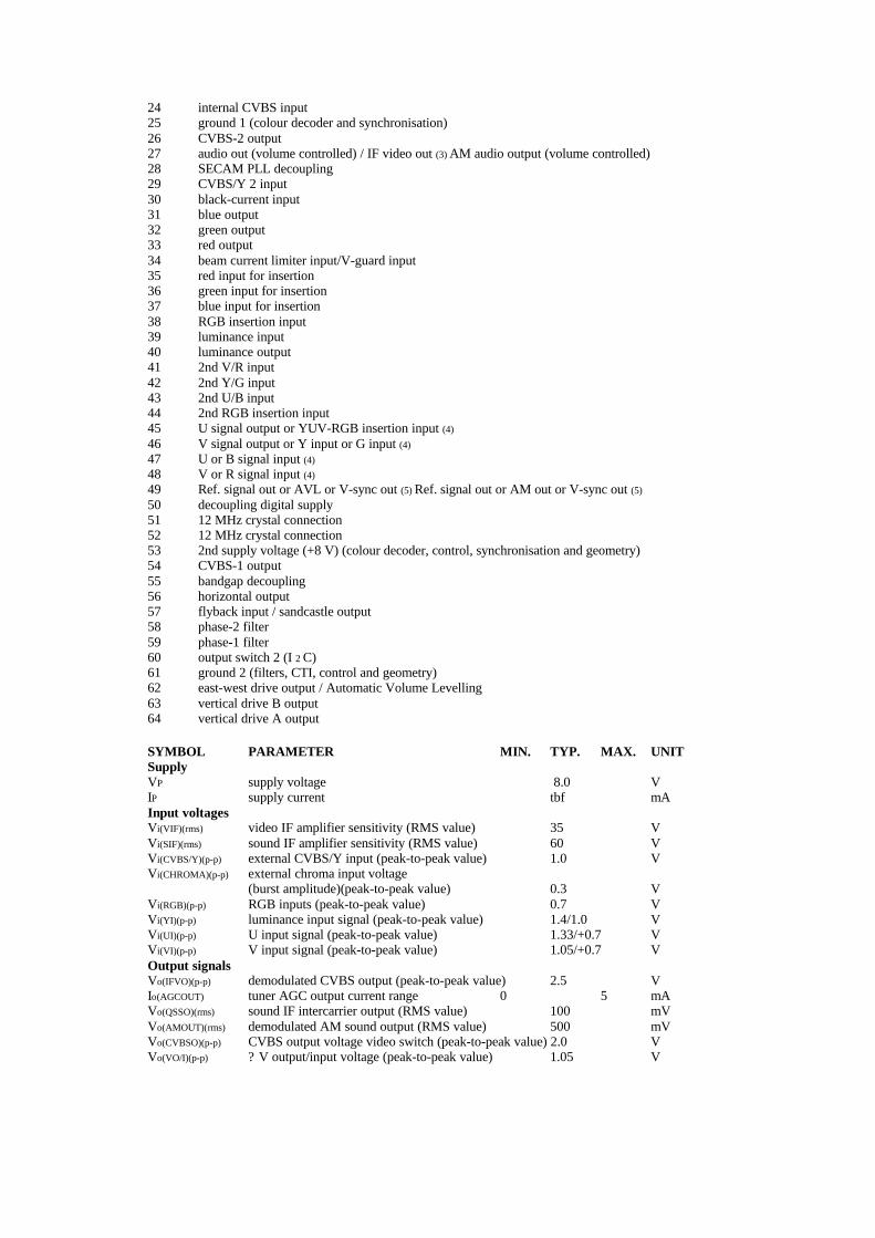
50 decoupling digital supply51 12 MHz crystal connection52 12 MHz crystal connection53 2nd supply voltage (+8 V) (colour decoder, control, synchronisation and geometry)54 CVBS-1 output55 bandgap decoupling56 horizontal output57 flyback input / sandcastle output58 phase-2 filter59 phase-1 filter60 output switch 2 (I 2 C)61 ground 2 (filters, CTI, control and geometry)62 east-west drive output / Automatic Volume Levelling63 vertical drive B output64 vertical drive A output
SYMBOL PARAMETER MIN. TYP. MAX. UNITSupplyVP supply voltage 8.0 VIP supply current tbf mAInput voltagesVi(VIF)(rms) video IF amplifier sensitivity (RMS value) 35 VVi(SIF)(rms) sound IF amplifier sensitivity (RMS value) 60 VVi(CVBS/Y)(p-p) external CVBS/Y input (peak-to-peak value) 1.0 VVi(CHROMA)(p-p) external chroma input voltage
(burst amplitude)(peak-to-peak value) 0.3 VVi(RGB)(p-p) RGB inputs (peak-to-peak value) 0.7 VVi(YI)(p-p) luminance input signal (peak-to-peak value) 1.4/1.0 VVi(UI)(p-p) U input signal (peak-to-peak value) 1.33/+0.7 VVi(VI)(p-p) V input signal (peak-to-peak value) 1.05/+0.7 VOutput signalsVo(IFVO)(p-p) demodulated CVBS output (peak-to-peak value) 2.5 VIo(AGCOUT) tuner AGC output current range 0 5 mAVo(QSSO)(rms) sound IF intercarrier output (RMS value) 100 mVVo(AMOUT)(rms) demodulated AM sound output (RMS value) 500 mVVo(CVBSO)(p-p) CVBS output voltage video switch (peak-to-peak value) 2.0 VVo(VO/I)(p-p) ? V output/input voltage (peak-to-peak value) 1.05 V
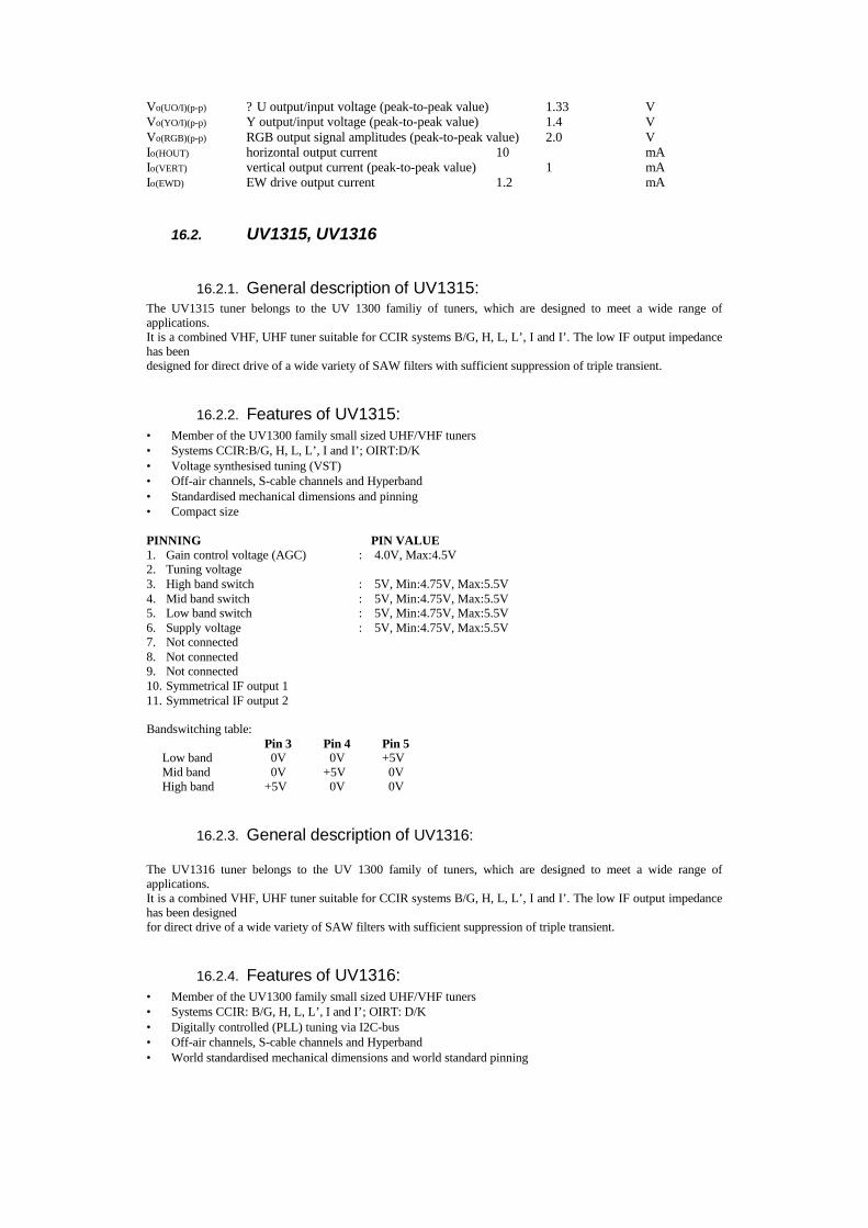
Vo(UO/I)(p-p) ? U output/input voltage (peak-to-peak value) 1.33 VVo(YO/I)(p-p) Y output/input voltage (peak-to-peak value) 1.4 VVo(RGB)(p-p) RGB output signal amplitudes (peak-to-peak value) 2.0 VIo(HOUT) horizontal output current 10 mAIo(VERT) vertical output current (peak-to-peak value) 1 mAIo(EWD) EW drive output current 1.2 mA
16.2. UV1315, UV1316
16.2.1. General description of UV1315:The UV1315 tuner belongs to the UV 1300 familiy of tuners, which are designed to meet a wide range ofapplications.It is a combined VHF, UHF tuner suitable for CCIR systems B/G, H, L, L’, I and I’. The low IF output impedancehas beendesigned for direct drive of a wide variety of SAW filters with sufficient suppression of triple transient.
16.2.2. Features of UV1315:• Member of the UV1300 family small sized UHF/VHF tuners• Systems CCIR:B/G, H, L, L’, I and I’; OIRT:D/K• Voltage synthesised tuning (VST)• Off-air channels, S-cable channels and Hyperband• Standardised mechanical dimensions and pinning• Compact size
PINNING PIN VALUE1. Gain control voltage (AGC) : 4.0V, Max:4.5V2. Tuning voltage3. High band switch : 5V, Min:4.75V, Max:5.5V4. Mid band switch : 5V, Min:4.75V, Max:5.5V5. Low band switch : 5V, Min:4.75V, Max:5.5V6. Supply voltage : 5V, Min:4.75V, Max:5.5V7. Not connected8. Not connected9. Not connected10. Symmetrical IF output 111. Symmetrical IF output 2
Bandswitching table:Pin 3 Pin 4 Pin 5
Low band 0V 0V +5VMid band 0V +5V 0VHigh band +5V 0V 0V
16.2.3. General description of UV1316:
The UV1316 tuner belongs to the UV 1300 family of tuners, which are designed to meet a wide range ofapplications.It is a combined VHF, UHF tuner suitable for CCIR systems B/G, H, L, L’, I and I’. The low IF output impedancehas been designedfor direct drive of a wide variety of SAW filters with sufficient suppression of triple transient.
16.2.4. Features of UV1316:• Member of the UV1300 family small sized UHF/VHF tuners• Systems CCIR: B/G, H, L, L’, I and I’; OIRT: D/K• Digitally controlled (PLL) tuning via I2C-bus• Off-air channels, S-cable channels and Hyperband• World standardised mechanical dimensions and world standard pinning
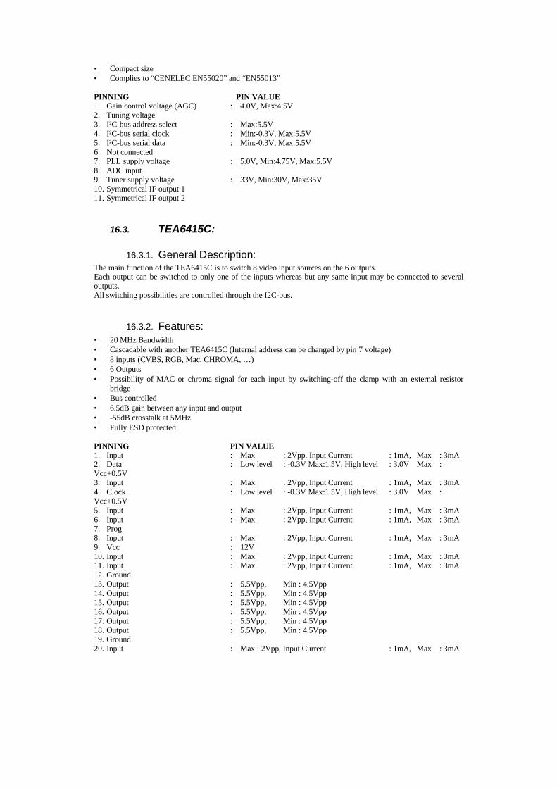
• Compact size• Complies to “CENELEC EN55020” and “EN55013”
PINNING PIN VALUE1. Gain control voltage (AGC) : 4.0V, Max:4.5V2. Tuning voltage3. I²C-bus address select : Max:5.5V4. I²C-bus serial clock : Min:-0.3V, Max:5.5V5. I²C-bus serial data : Min:-0.3V, Max:5.5V6. Not connected7. PLL supply voltage : 5.0V, Min:4.75V, Max:5.5V8. ADC input9. Tuner supply voltage : 33V, Min:30V, Max:35V10. Symmetrical IF output 111. Symmetrical IF output 2
16.3. TEA6415C:
16.3.1. General Description:The main function of the TEA6415C is to switch 8 video input sources on the 6 outputs.Each output can be switched to only one of the inputs whereas but any same input may be connected to severaloutputs.All switching possibilities are controlled through the I2C-bus.
16.3.2. Features:• 20 MHz Bandwidth• Cascadable with another TEA6415C (Internal address can be changed by pin 7 voltage)• 8 inputs (CVBS, RGB, Mac, CHROMA, … )• 6 Outputs• Possibility of MAC or chroma signal for each input by switching-off the clamp with an external resistor
bridge• Bus controlled• 6.5dB gain between any input and output• -55dB crosstalk at 5MHz• Fully ESD protected
PINNING PIN VALUE1. Input : Max : 2Vpp, Input Current : 1mA, Max : 3mA2. Data : Low level : -0.3V Max:1.5V, High level : 3.0V Max :Vcc+0.5V3. Input : Max : 2Vpp, Input Current : 1mA, Max : 3mA4. Clock : Low level : -0.3V Max:1.5V, High level : 3.0V Max :Vcc+0.5V5. Input : Max : 2Vpp, Input Current : 1mA, Max : 3mA6. Input : Max : 2Vpp, Input Current : 1mA, Max : 3mA7. Prog8. Input : Max : 2Vpp, Input Current : 1mA, Max : 3mA9. Vcc : 12V10. Input : Max : 2Vpp, Input Current : 1mA, Max : 3mA11. Input : Max : 2Vpp, Input Current : 1mA, Max : 3mA12. Ground13. Output : 5.5Vpp, Min : 4.5Vpp14. Output : 5.5Vpp, Min : 4.5Vpp15. Output : 5.5Vpp, Min : 4.5Vpp16. Output : 5.5Vpp, Min : 4.5Vpp17. Output : 5.5Vpp, Min : 4.5Vpp18. Output : 5.5Vpp, Min : 4.5Vpp19. Ground20. Input : Max : 2Vpp, Input Current : 1mA, Max : 3mA
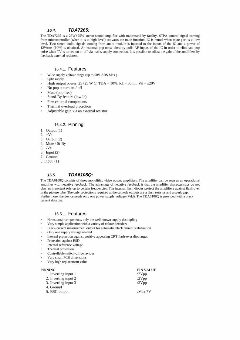
16.4. TDA7265:The TDA7265 is a 25W+25W stereo sound amplifier with mute/stand-by facility. STPA control signal comingfrom microcontroller (when it is at high level) activates the mute function. IC is muted when mute port is at lowlevel. Two stereo audio signals coming from audio module is injected to the inputs of the IC and a power of12Wrms (10%) is obtained. An external pop-noise circuitry pulls AF inputs of the IC in order to eliminate popnoise when TV is turned on or off via mains supply connection. It is possible to adjust the gain of the amplifiers byfeedback external resistors.
16.4.1. Features:• Wide supply voltage range (up to 50V ABS Max.)• Split supply• High output power: 25+25 W @ TDA = 10%, RL = 8ohm, VS = ±20V• No pop at turn-on / off• Mute (pop free)• Stand-By feature (low IQ)• Few external components• Thermal overload protection• Adjustable gain via an external resistor
16.4.2. Pinning:1. Output (1)2. +Vs3. Output (2)4. Mute / St-By5. -Vs6. Input (2)7. Ground8. Input (1)
16.5. TDA6108Q:The TDA6108Q consists of three monolithic video output amplifiers. The amplifier can be seen as an operationalamplifier with negative feedback. The advantage of negative feedback is that the amplifier characteristics do notplay an important role up to certain frequencies. The internal flash diodes protect the amplifiers against flash overin the picture tube. The only protections required at the cathode outputs are a flash resistor and a spark gap.Furthermore, the device needs only one power supply voltage (Vdd). The TDA6108Q is provided with a blackcurrent data pin.
16.5.1. Features:• No external components, only the well known supply decoupling• Very simple application with a variety of colour decoders• Black-current measurement output for automatic black current stabilisation• Only one supply voltage needed• Internal protection against positive appearing CRT flash-over discharges• Protection against ESD• Internal reference voltage• Thermal protection• Controllable switch-off behaviour• Very small PCB dimensions• Very high replacement value
PINNING PIN VALUE1. Inverting input 1 :2Vpp2. Inverting input 2 :2Vpp3. Inverting input 3 :2Vpp4. Ground5. BSC-output :Max:7V
6. Supply voltage :200VDC7. Cathode output 3 :20mA, 100Vpp8. Cathode output 2 :20mA, 100Vpp9. Cathode output 1 :20mA, 100Vpp
16.6. 74 HCT 32The 74HC/HCT32 are high-speed Si-gate CMOS devices and are pin compatible with low power SchottkyTTL (LSTTL). They are specified in compliance with JEDEC. The 74HC/HCT32 provide the 2-input ORfunction.
16.6.1. PINNING 1, 4, 9, 12 : 1A to 4A data inputs2, 5, 10, 13 : 1B to 4B data inputs3, 6, 8, 11 : 1Y to 4Y data outputs7 : GND ground (0 V)14 : VCC positive supply voltage
For HC the condition is VI = GND to VCC
For HCT the condition is VI = GND to VCC ? ? 1.5 V
16.7. MC44608
16.7.1. General description:The MC44608 is a high performance voltage mode controller designed for off–line converters. Thishigh voltage circuit that integrates the start–up current source and the oscillator capacitor, requires fewexternal components while offering a high flexibility and reliability.The device also features a very high efficiency stand–by management consisting of an effective Pulsed Modeoperation. This technique enables the reduction of the stand–by power consumption to approximately 1W whiledelivering 300mW in a 150W SMPS.
• Integrated start–up current source• Lossless off–line start–up• Direct off–line operation• Fast start–up
16.7.2. General Features• Flexibility• Duty cycle control• On chip oscillator switching frequency 40, or 75kHz• Secondary control with few external componentsProtections• Maximum duty cycle limitation• Cycle by cycle current limitation• Demagnetisation (Zero current detection) protection• “Over V CC protection” against open loop• Programmable low inertia over voltage protection against open loop• Internal thermal protectionGreenLine Controller• Pulsed mode techniques for a very high efficiency low power mode• Lossless start-up• Low dV/dT for low EMI radiation's
PINNING PIN VALUE1. Demagnetisation Zero cross detection voltage: 50 mV typ.2. I Sense Over current protection voltage 1V typ.
3. Control Input Min: 7.5V Max.: 18V4. Ground Iout 2Ap-p during scan 1.2Ap-p during flyback5. Driver Output resistor 8.5 Ohm sink 15 Ohm source typ.6. Supply voltage Max:16V (Operating range 6.6V-13V)7. No connection8. Line Voltage Min:50V Max:500V
16.8. SDA5555:
16.8.1. General description:• Feature selection via special function register• Simultaneous reception of TTX, VPS, PDC, and WSS (line 23)• Supply Voltage 2.5 and 3.3 V
PINNING1 Comb Filter Standard Selection 1 Low Level : 0V High Level : 3.3 V2 Key 2 Low Level : 0V High Level : 3.3 V3 Key 1 Low Level : 0V High Level : 3.3 V4 Loc.key.switch input Low Level : 0V High Level : 3.3 V5 Loc.key.switch input Low Level : 0V High Level : 3.3 V6 Loc.key.switch input Low Level : 0V High Level : 3.3 V7 Loc.key.switch input Low Level : 0V High Level : 3.3 V8 Mute output Low Level : 0V High Level : 3.3 V9 Digital supply voltage 2.5 V10 Ground11 Digital supply voltage 3.3 V12 CVBS input 1 Vpp13 Analogue supply voltage 2.5 V14 Analogue ground15 Wake Interrupt Low Level : 0V High Level : 3.3 V16 AV-1 status input Low Level : 0V High Level : 3.3 V17 AV-2 status input Low Level : 0V High Level : 3.3 V18 Shortcut protection Low Level : 0V High Level : 3.3 V19 SAND input Low Level : 0V High Level : 3.3 V20 ODD/EVEN output Low Level : 0V High Level : 3.3 V21 DVD 12 V Sense Low Level : 0V High Level : 3.3 V22 Not used23 Idle Off Low Level : 0V High Level : 3.3 V24 IR-input Low Level : 0V High Level : 3.3 V25 Data output Low Level : 0V High Level : 3.3 V26 Clock signal output Low Level : 0V High Level : 3.3 V27 Stand-By Mode selection Low Level : 0V High Level : 3.3 V28 Not used29 Ground30 Digital supply voltage 3.3 V31 Write Protect output Low Level : 0V High Level : 3.3 V32 Service output Low Level : 0V High Level : 3.3 V33 Reset output Low Level : 0V High Level : 3.3 V34 6 MHz cristal connection 2 Low Level : 0V High Level : 3.3 V35 6 MHz cristal connection 1 Low Level : 0V High Level : 3.3 V36 Analogue ground37 Analogue supply voltage 2.5 V38 OSD-Red output 0.7 Vpp to 1.2 Vpp
39 OSD-Green output 0.7 Vpp to 1.2 Vpp40 OSD-Blue output 0.7 Vpp to 1.2 Vpp41 OSD-Blanking output Low Level : 0V High Level : 3.3 V42 Digital supply voltage 2.5 V43 Ground44 Digital supply voltage 3.3 V45 PAL / SECAM Low Level : 0V High Level : 3.3 V46 Degauss Low Level : 0V High Level : 3.3 V47 Horizontal Trapezoid Low Level : 0V High Level : 3.3 V48 Tilt Low Level : 0V High Level : 3.3 V49 Not used50 Micro s. select Low Level : 0V High Level : 3.3 V51 Comb Filter Standard Selection 2 Low Level : 0V High Level : 3.3 V52 SVHS Sense Low Level : 0V High Level : 3.3 V
16.9. TDA9181:Pin#:Pin-1 = Cýn=Chrominance input signalPin-2 = INPSEL=input switch select inputPin-3 =Y/CVBS2=luminance or CVBS input signal 2Pin-4 = Digital GNDPin-5= VDD=digital supply voltagePin-6=VCC=analog supply voltagePin-7 =SC=sandcastle input signalPin-8 =FSCSEL=color subcarrier select inputPin-9 = FSC=color subcarrier input signalPin-10 =SYS2=standart select 2 inputPin-11 = SYS1=standart select 1 inputPin-12 =Y/CVBS1=luminance or CVBS input signalPin-13 = analogue GNDPin-14 = Y/CVBSout=luminance or CVBS output signalPin-15 =OUTSEL=output switch select inputPin-16 =Cout=chrominance output signal
16.9.1. General Features:-One chip multistandart adaptive comb filter-Cross luminance reduction-Cross colour reduction-No chroma trap, so sharper vertical luminance-Analogue discrete-time signal processing, so no quantization noise-Anti aliasing and reconstruction filters are included-Input switch selects between two Y/CVBS inputs-Output switch selects between combed CVBS and an external Y/C source-Fsc as well as 2*fsc colour subcarrier signal may be applied-Alignment free-Few external components-Low power
16.9.2. Limits:-Analogue supply voltage Vcc=5.5V(max)-Analogue supply current Icc=25mA(typ)-Digital supply voltage Vdd=5.5(V)(max)-Digital supply current Idd=10Ma(typ)-Luminance or CVBS input signal (p-p) Y/CVBS1, 2 1.4V(max)
-Chrominance input signal (p-p) Cin=1.0V(max)
16.10. TCD1102:
16.10.1. DescriptionThe TCET110./ TCET2100/ TCET4100 consists of a phototransistor optically coupled to a galliumarsenide infrared emitting diode in a 4-lead plastic dual inline package. The elements are mounted onone leadframe using acoplanar technique, providing a fixed distances between input and output for highest safetyrequirements.
16.10.2. ApplicationsCircuits for safe protective separation against electrical shock according to safety class II (reinforcedisolation): For appl. class I – IV at mains voltage ? 300 V For appl. class I – III at mains voltage ? 600 Vaccording to VDE 0884, table 2, suitable for:Switch-mode power supplies, line receiver, computerperipheral interface, microprocessor system interfaces.
VDE 0884 related features: Rated impulse voltage (transient overvoltage) V IOTM = 8 kV peak Isolation test voltage (partial discharge test voltage) V pd = 1.6 kV Rated isolation voltage (RMS includes DC) V IOWM = 600 V RMS (848 V peak) Rated recurring peak voltage (repetitive) V IORM = 600 V RMS
16.10.3. General features: CTR offered in 9 groups Isolation materials according to UL94-VO Pollution degree 2 (DIN/VDE 0110 / resp. IEC 664) Climatic classification 55/100/21 (IEC 68 part 1) Special construction: Therefore, extra low coupling capacity of typical 0.2 pF, high Common ModeRejection Low temperature coefficient of CTR G = Leadform 10.16 mm; provides creepage distance > 8 mm, for TCET2100/ TCET4100 optional;suffix letter ‘G’ is not marked on the optocoupler Coupling System U
16.11. ST24C08:
16.11.1. General description:The ST24C08 is an 8Kbit electrically erasable programmable memory (EEPROM), organised as 4 blocks of 256 *8 bits.The memory operates with a power supply value as low as 2.5V. Both Plastics Dual-in-Line and Plastic SmallOutline packagesare available.
16.11.2. Features:• Minimum 1 million ERASE/WRITE cycles with over 10 years data retention• Single supply voltage:4.5 to 5.5V• Two wire serial interface, fully I2C-bus compatible• Byte and Multibyte write (up to 8 bytes)
• Page write (up to 16 bytes)• Byte, random and sequential read modes• Self timed programming cycle
PINNING PIN VALUE1. Write protect enable (Ground) : 0V2. Not connected (Ground) : 0V3. Chip enable input (Ground) : 0V4. Ground : 0V5. Serial data address input/output : Input LOW voltage : Min : -0.3V, Max : 0.3*Vcc
Input HIGH voltage: Min : 0.7*Vcc, Max : Vcc+16. Serial clock : Input LOW voltage : Min: -0.3V, Max : 0.3*Vcc
Input HIGH voltage: Min : 0.7*Vcc, Max : Vcc+17. Multibyte/Page write mode : Input LOW voltage : Min: -0.3V, Max :0.5V
Input HIGH voltage: Min : Vcc-0.5, Max : Vcc+18. Supply voltage : Min : 2.5V, Max : 5.5V
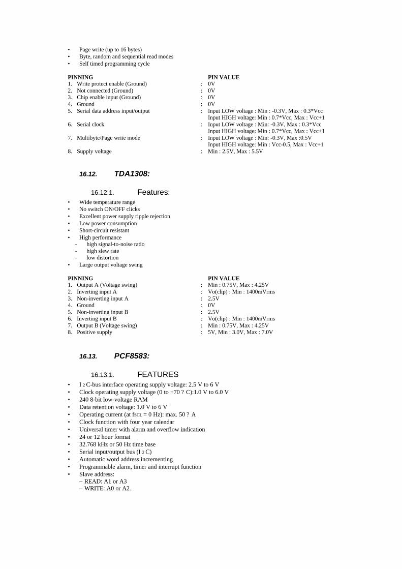
16.12. TDA1308:
16.12.1. Features:• Wide temperature range• No switch ON/OFF clicks• Excellent power supply ripple rejection• Low power consumption• Short-circuit resistant• High performance
- high signal-to-noise ratio- high slew rate- low distortion
• Large output voltage swing
PINNING PIN VALUE1. Output A (Voltage swing) : Min : 0.75V, Max : 4.25V2. Inverting input A : Vo(clip) : Min : 1400mVrms3. Non-inverting input A : 2.5V4. Ground : 0V5. Non-inverting input B : 2.5V6. Inverting input B : Vo(clip) : Min : 1400mVrms7. Output B (Voltage swing) : Min : 0.75V, Max : 4.25V8. Positive supply : 5V, Min : 3.0V, Max : 7.0V
16.13. PCF8583:
16.13.1. FEATURES• I 2 C-bus interface operating supply voltage: 2.5 V to 6 V• Clock operating supply voltage (0 to +70 ? C):1.0 V to 6.0 V• 240 8-bit low-voltage RAM• Data retention voltage: 1.0 V to 6 V• Operating current (at fSCL = 0 Hz): max. 50 ? A• Clock function with four year calendar• Universal timer with alarm and overflow indication• 24 or 12 hour format• 32.768 kHz or 50 Hz time base• Serial input/output bus (I 2 C)• Automatic word address incrementing• Programmable alarm, timer and interrupt function• Slave address:
– READ: A1 or A3– WRITE: A0 or A2.
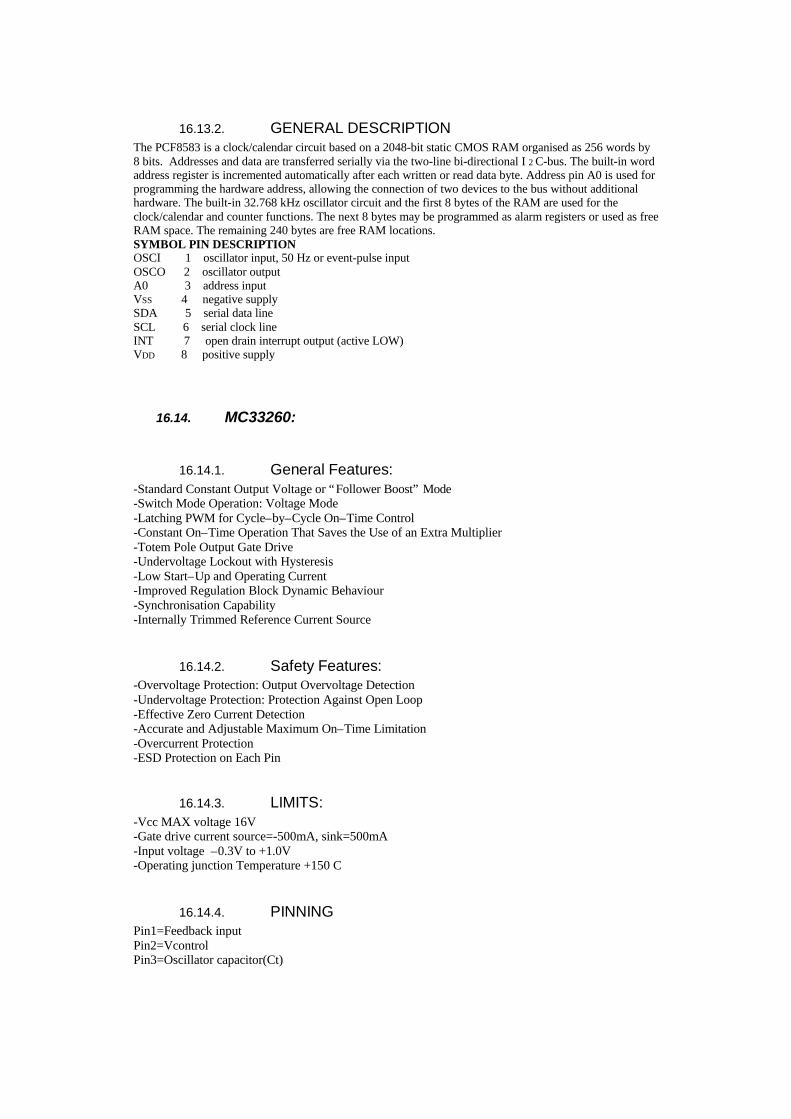
16.13.2. GENERAL DESCRIPTIONThe PCF8583 is a clock/calendar circuit based on a 2048-bit static CMOS RAM organised as 256 words by8 bits. Addresses and data are transferred serially via the two-line bi-directional I 2 C-bus. The built-in wordaddress register is incremented automatically after each written or read data byte. Address pin A0 is used forprogramming the hardware address, allowing the connection of two devices to the bus without additionalhardware. The built-in 32.768 kHz oscillator circuit and the first 8 bytes of the RAM are used for theclock/calendar and counter functions. The next 8 bytes may be programmed as alarm registers or used as freeRAM space. The remaining 240 bytes are free RAM locations.SYMBOL PIN DESCRIPTIONOSCI 1 oscillator input, 50 Hz or event-pulse inputOSCO 2 oscillator outputA0 3 address inputVSS 4 negative supplySDA 5 serial data lineSCL 6 serial clock lineINT 7 open drain interrupt output (active LOW)VDD 8 positive supply
16.14. MC33260:
16.14.1. General Features:-Standard Constant Output Voltage or “Follower Boost” Mode-Switch Mode Operation: Voltage Mode-Latching PWM for Cycle–by–Cycle On–Time Control-Constant On–Time Operation That Saves the Use of an Extra Multiplier-Totem Pole Output Gate Drive-Undervoltage Lockout with Hysteresis-Low Start–Up and Operating Current-Improved Regulation Block Dynamic Behaviour-Synchronisation Capability-Internally Trimmed Reference Current Source
16.14.2. Safety Features:-Overvoltage Protection: Output Overvoltage Detection-Undervoltage Protection: Protection Against Open Loop-Effective Zero Current Detection-Accurate and Adjustable Maximum On–Time Limitation-Overcurrent Protection-ESD Protection on Each Pin
16.14.3. LIMITS:-Vcc MAX voltage 16V-Gate drive current source=-500mA, sink=500mA-Input voltage –0.3V to +1.0V-Operating junction Temperature +150 C
16.14.4. PINNINGPin1=Feedback inputPin2=VcontrolPin3=Oscillator capacitor(Ct)
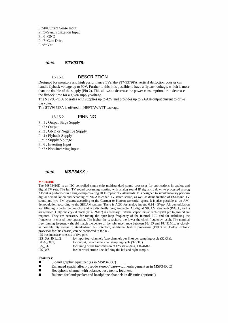
Pin4=Current Sense InputPin5=Synchronization InputPin6=GNDPin7=Gate DrivePin8=Vcc
16.15. STV9379:
16.15.1. DESCRIPTIONDesigned for monitors and high performance TVs, the STV9379FA vertical deflection booster canhandle flyback voltage up to 90V. Further to this, it is possible to have a flyback voltage, which is morethan the double of the supply (Pin 2). This allows to decrease the power consumption, or to decreasethe flyback time for a given supply voltage.The STV9379FA operates with supplies up to 42V and provides up to 2.6APP output current to drivethe yoke.The STV9379FA is offered in HEPTAWATT package.
16.15.2. PINNINGPin1 : Output Stage SupplyPin2 : OutputPin3 : GND or Negative SupplyPin4 : Flyback SupplyPin5 : Supply VoltagePin6 : Inverting InputPin7 : Non-inverting Input
16.16. MSP34XX :
MSP3410DThe MSP3410D is an I2C controlled single-chip multistandard sound processor for applications in analog anddigital TV sets. The full TV sound processing, starting with analog sound IF signal-in, down to processed analogAF-out is performed in a single-chip covering all European TV-standards. It is designed to simultaneously performdigital demodulation and decoding of NICAM-coded TV stereo sound, as well as demodulation of FM-mono TVsound and two FM systems according to the German or Korean terrestrial specs. It is also possible to do AM-demodulation according to the SECAM system. There is AGC for analog inputs: 0.14 - 3Vpp. All demodulationand filtering is performed on chip and is individually programmable. All digital NICAM standards (B/G, L, and I)are realised. Only one crystal clock (18.432Mhz) is necessary. External capacitors at each crystal pin to ground arerequired. They are necessary for tuning the open-loop frequency of the internal PLL and for stabilising thefrequency in closed-loop operation. The higher the capacitors, the lower the clock frequency result. The nominalfree running frequency should match the centre of the tolerance range between 18.433 and 18.431Mhz as closelyas possible. By means of standardised I2S interface, additional feature processors (DPL35xx, Dolby Prologicprocessor for this chassis) can be connected to the IC.I2S bus interface consists of five pins:I2S_DA_IN1… 2 for input four channels (two channels per line) per sampling cycle (32Khz).I2DA_OUT, for output, two channels per sampling cycle (32KHz).I2S_CL, for timing of the transmission of I2S serial data, 1.024Mhz.I2S_WS, for the word strobe line defining the left and right sample.
Features:n 5-band graphic equalizer (as in MSP3400C)n Enhanced spatial affect (pseudo stereo / base-width enlargement as in MSP3400C)n Headphone channel with balance, bass treble, loudnessn Balance for loudspeaker and headphone channels in dB units (optional)
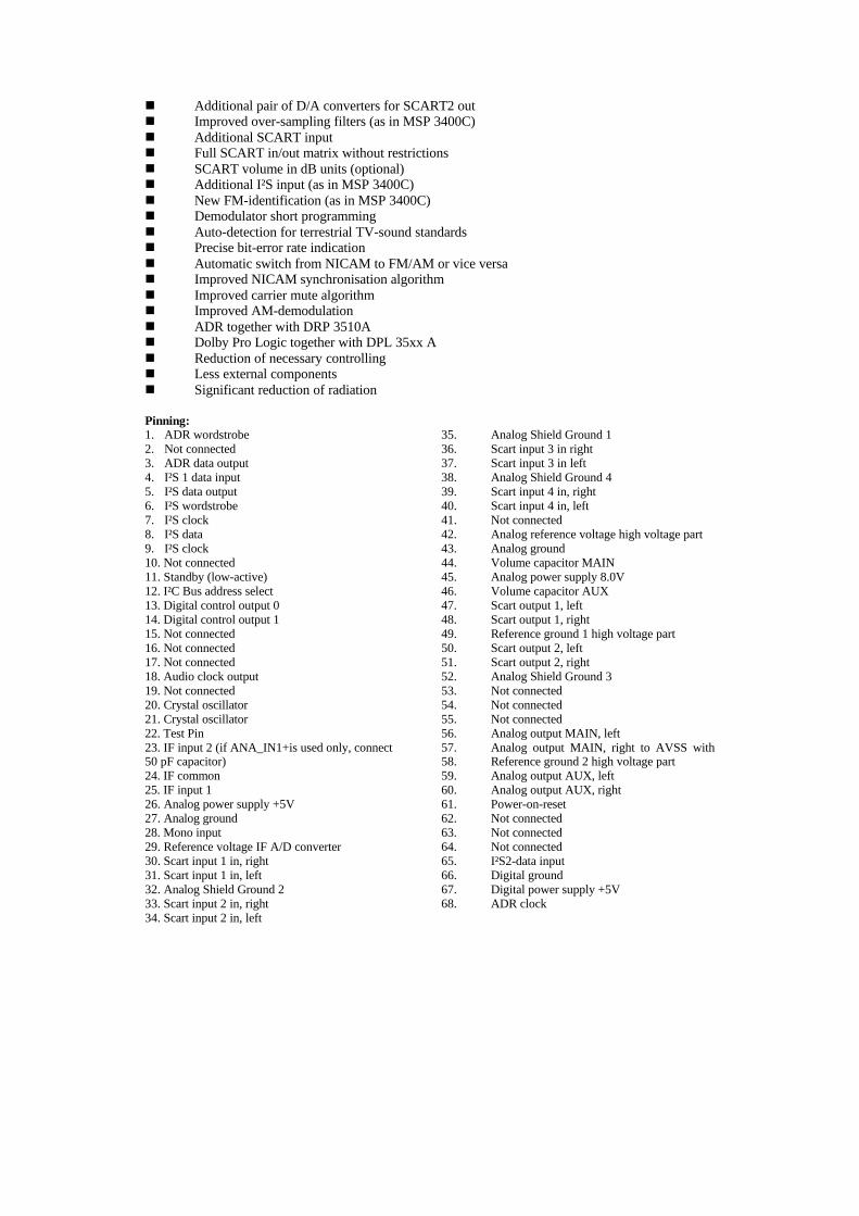
n Additional pair of D/A converters for SCART2 outn Improved over-sampling filters (as in MSP 3400C)n Additional SCART inputn Full SCART in/out matrix without restrictionsn SCART volume in dB units (optional)n Additional I²S input (as in MSP 3400C)n New FM-identification (as in MSP 3400C)n Demodulator short programmingn Auto-detection for terrestrial TV-sound standardsn Precise bit-error rate indicationn Automatic switch from NICAM to FM/AM or vice versan Improved NICAM synchronisation algorithmn Improved carrier mute algorithmn Improved AM-demodulationn ADR together with DRP 3510An Dolby Pro Logic together with DPL 35xx An Reduction of necessary controllingn Less external componentsn Significant reduction of radiation
Pinning:1. ADR wordstrobe 35. Analog Shield Ground 12. Not connected 36. Scart input 3 in right3. ADR data output 37. Scart input 3 in left4. I²S 1 data input 38. Analog Shield Ground 45. I²S data output 39. Scart input 4 in, right6. I²S wordstrobe 40. Scart input 4 in, left7. I²S clock 41. Not connected8. I²S data 42. Analog reference voltage high voltage part9. I²S clock 43. Analog ground10. Not connected 44. Volume capacitor MAIN11. Standby (low-active) 45. Analog power supply 8.0V12. I²C Bus address select 46. Volume capacitor AUX13. Digital control output 0 47. Scart output 1, left14. Digital control output 1 48. Scart output 1, right15. Not connected 49. Reference ground 1 high voltage part16. Not connected 50. Scart output 2, left17. Not connected 51. Scart output 2, right18. Audio clock output 52. Analog Shield Ground 319. Not connected 53. Not connected20. Crystal oscillator 54. Not connected21. Crystal oscillator 55. Not connected22. Test Pin 56. Analog output MAIN, left23. IF input 2 (if ANA_IN1+is used only, connect 57. Analog output MAIN, right to AVSS with50 pF capacitor) 58. Reference ground 2 high voltage part24. IF common 59. Analog output AUX, left25. IF input 1 60. Analog output AUX, right26. Analog power supply +5V 61. Power-on-reset27. Analog ground 62. Not connected28. Mono input 63. Not connected29. Reference voltage IF A/D converter 64. Not connected30. Scart input 1 in, right 65. I²S2-data input31. Scart input 1 in, left 66. Digital ground32. Analog Shield Ground 2 67. Digital power supply +5V33. Scart input 2 in, right 68. ADR clock34. Scart input 2 in, left
16.17. LM358N:
16.17.1. General DescriptionThe LM158 series consists of two independent, high gain, internally frequency compensated operational amplifierswhich were designed specifically to operate from a single power supply over a wide range of voltages. Operation fromsplit power supplies is also possible and the low power supply current drain is independent of the magnitude of the powersupply voltage. Application areas include transducer amplifiers, dc gain blocks and all the conventional op amp circuits,which now can be more easily implemented in single power supply systems. For example, the LM158 series can bedirectly operated off of the standard +5V power supply voltage, which is used in digital systems and will easily providethe required interface electronics without requiring the additional ±15V power supplies.
16.17.2. Unique Characteristics In the linear mode the input common-mode voltage range includes ground and the output voltage can also swing toground, even though operated from only a single power supply voltage. The unity gain cross frequency is temperature compensated. The input bias current is also temperature compensated.
16.17.3. Advantages Two internally compensated op amps Eliminates need for dual supplies Allows direct sensing near GND and VOUT also goes to GND Compatible with all forms of logic Power drain suitable for battery operation Pin-out same as LM1558/LM1458 dual op amp
16.17.4. Features Available in 8-Bump micro SMD chip sized package, Internally frequency compensated for unity gain n Large dcvoltage gain: 100 dB Wide bandwidth (unity gain): 1 MHz (temperature compensated) Wide power supply range:
— Single supply: 3V to 32V— or dual supplies: ±1.5V to ±16V
Very low supply current drain (500 µA) — essentially independent of supply voltage Low input offset voltage: 2 mV Input common-mode voltage range includes ground Differential input voltage range equal to the power supply voltage Large output voltage swing: 0V to V + þ 1.5V
17. AK33 CHASSIS MANUAL ADJUSTMENTS PROCEDUREIn order to enter the service menu, first enter the installation menu and then press the digits 4, 7, 2 and 5
respectively.
For ADJUST settings:Select Adjust using or button and press or button to enter it. To select different adjust parameters, use or button.To change the selected parameter, use or button.WHITE BALANCE ADJUSTMENT:The following three parameters are used to make white balance adjustment. To do this, use a Colour Analyser.Using white point RED, white point GREEN and white point BLUE parameters, insert the + sign in the squarewhich is in the middle of the screen.ADJUST 00 = White Point REDADJUST 01 = White Point GREENADJUST 02 = White Point BLUE
AGC ADJUSTMENT:In order to do AGC adjustment, enter a 60dBmV RF signal level from channel C-12.Connect a digital voltmeter to pin 1 of the tuner. Change the AGC parameter until you see 3.70VDC on voltmeterdisplay. Check that picture is normal at 90dBmV signal level.ADJUST 03 = AGC
IF-PLL NEGATIVE ADJUSTMENT (Only with PLL tuner):
Connect 38.9 MHz test pattern for PAL B/G, PAL-SECAM B/G, 39.5 MHz test pattern for PAL I or 45.75 MHztest pattern forPAL M/N, NTSC M model to Z401 SAW filter input terminals. Change the IF-PLL Negative parameter until yousee IN, DOWN below. If you cannot catch IN, DOWN position this way, using a screwdriver rotate the VIF-COILLT401 left or right until yousee IN, DOWN.ADJUST 04 = IF-PLL Negative
IF-PLL POSITIVE ADJUSTMENT (Only with PLL tuner):Connect 33.9 MHz test pattern for SECAM L’ model to Z401 SAW filter input terminals. Change the IF-PLLPositive parameteruntil you see IN, DOWN below. If you cannot catch IN, DOWN position this way, using a screwdriver rotate theVIF-COIL LT401left or right until you see IN, DOWN.ADJUST 05 = IF-PLL Positive
LUMINANCE DELAY ADJUSTMENT (with only TDA 8844 video processor):ADJUST 06 = Y-Delay PALEnter a PAL B/G colour and black-white bar test pattern via RF. Adjust Y-Delay PAL till the colour transients onthe colour bar ofthe pattern become as sharper and colours between transients do not mix with each other as possible.Note: If the SAW filter is one of the G1965M, J1951M, J3950M, K2958M, K2962M, G3957M, K6256K,K6259K or M1963M, there is constant group delay distortion, so for an equal delay of the luminance andchrominance signal the delay must be set at avalue of 160nS. This means the adjustment must be set to the maximum value.ADJUST 07 = Y-Delay SECAMEnter a SECAM B/G colour and black-white bar test pattern via RF. Adjust Y-Delay SECAM till the colourtransients on the colour bar of the pattern become as sharper and colours between transients do not mix with eachother as possible.Note: If the SAW filter is one of the G1965M, K2958M, K2962M, G3957M, K6256K or K6259K, there isconstant group delay distortion, so for an equal delay of the luminance and chrominance signal the delay must beset at a value of 160nS.This means the adjustment must be set to the maximum value.ADJUST 08 = Y-Delay NTSCEnter an NTSC colour and black-white bar test pattern via RF. Adjust Y-Delay NTSC till the colour transients onthe colour barof the pattern become as sharper and colours between transients do not mix with each other as possible.Note: If the SAW filter is M1963M, there is constant group delay distortion, so for an equal delay of theluminance and chrominance signal the delay must be set at a value of 160nS. This means the adjustment must beset to the maximum value.ADJUST 09 = Y-Delay OtherIn case of other colour systems, enter this system with colour and black-white bar test pattern via RF. Adjust Y-Delay Other till the colour transients on the colour bar of the pattern become as sharper and colours betweentransients do not mix with each otheras possible. Normally for an equal delay of the luminance and chrominance signal the delay must be set at a valueof 160nS.This means the adjustment must be set to the maximum value.
VERTICAL ZOOM ADJUSTMENT (only for 110ø picture tubes):ADJUST 10 = Vertical ZoomEnter a PAL B/G circle test pattern via RF. Change vertical zoom till you see the upper and lower limit of thecircle as close to the upper and lower limit of the picture tube as possible.
VERTICAL SCROLL ADJUSTMENT (only for 110ø picture tubes):ADJUST 11 = Vertical ScrollEnter a PAL B/G circle test pattern via RF. Change vertical scroll till you see the circle exactly in the middle of thescreen.
4:3 HORIZONTAL SHIFT ADJUSTMENT:ADJUST 12 = 4 : 3 Horizontal ShiftEnter a RED PURITY test pattern via RF. Change horizontal shift till the picture is horizontally centred. Checkwhether this adjustment is correct after completing Service Mode Adjustment.
4:3 VERTICAL SLOPE ADJUSTMENT:ADJUST 13 = 4 : 3 Vertical Slope
Enter a CROSS-HATCH B/G test pattern via RF. Change vertical slope till the size of squares on both the upperand lower partof test pattern become equal to the squares laying on the vertical centre of the test pattern. Check and readjustVERTICALSLOPE item if the adjustment becomes improper after some other geometric adjustments are done.4:3 VERTICAL AMPLITUDE ADJUSTMENT:ADJUST 14 = 4 : 3 Vertical AmplitudeEnter a PAL B/G test pattern via RF. Change vertical slope till horizontal black lines on both the upper and lowerpart of the test pattern become very close to the upper and lower horizontal sides of picture tube and nearly aboutto disappear. Check and readjust VERTICAL AMPLITUDE item if the adjustment becomes improper after someother geometric adjustments are done.
4:3 S-CORRECTION ADJUSTMENT:ADJUST 15 = 4 : 3 S-CorrectionEnter a PAL B/G circle test pattern via RF. Change S-correction till the middle part of the circle is as round aspossible.
4:3 VERTICAL SHIFT ADJUSTMENT:ADJUST 16 = 4 : 3 Vertical ShiftEnter a PAL B/G test pattern via RF. Change Vertical Shift till the test pattern is vertically centred, i.e. horizontalline at the centre pattern is in equal distance both to upper and lower side of the picture tube. Check and readjustVertical Shift item if the adjustment becomes improper after some other geometric adjustments are done.
4:3 EW WIDTH ADJUSTMENT (only for 110ø picture tubes):ADJUST 17 = 4 : 3 EW WidthEnter a PAL B/G test pattern via RF. Change EW Width till the vertical black and white bars on both left and rightside of thepattern exactly disappear.
4:3 EW PARABOLA WIDTH ADJUSTMENT (only for 110ø picture tubes):ADJUST 18 = 4 : 3 EW Parabola WidthEnter a PAL B/G test pattern via RF. Change EW Parabola Width till vertical lines close to the both sides of thepicture frame become parallel to vertical sides of picture tube. Check and readjust EW Parabola Width item if theadjustment becomes improper after some other geometric adjustments are done.
4:3 EW UPPER CORNER PARABOLA ADJUSTMENT (only for 110ø picture tubes):ADJUST 19 = 4 : 3 EW Corner ParabolaEnter a PAL B/G test pattern via RF. Change EW Upper Corner Parabola till vertical lines at the corners of bothsides of picture frame become vertical and parallel to vertical corner sides of picture tube. Check and readjust EWUpper Corner Parabola item if the adjustment becomes improper after some other geometric adjustments are done.
4:3 EW TRAPEZIUM ADJUSTMENT :ADJUST 20 = 4 : 3 EW TrapeziumEnter a PAL B/G test pattern via RF. Change EW Trapezium till vertical lines, especially lines at the sides of thepicture frame became parallel to the both sides of picture tube as close as possible. Check and readjust EWTrapezium item if the adjustment becomes improper after some other geometric adjustments are done.
HORIZONTAL PARALLELOGRAM:ADJUST 21 = Horizontal ParallelogramEnter a PAL B/G test pattern via RF. Change Horizontal Parallelogram to set vertical lines orthogonal to thehorizontal lines Check and readjust Horizontal Parallelogram item if the adjustment becomes improper after someother geometric adjustments are done.
BOW :ADJUST 22 = BowEnter a PAL B/G test pattern via RF. Change Bow to straighten the vertical lines. Check and readjust Bow item ifthe adjustment becomes improper after some other geometric adjustments are done.
4:3 EW LOWER CORNER PARABOLA ADJUSTMENT (only for 110ø picture tubes):ADJUST 23 = 4 : 3 EW Lower Corner ParabolaEnter a PAL B/G test pattern via RF. Change EW Lower Corner Parabola till vertical lines at the corners of bothsides of picture frame become vertical and parallel to vertical corner sides of picture tube. Check and readjust EWLower Corner Parabola item if the adjustment becomes improper after some other geometric adjustments are done.

**remark that some adjustments are fixed to default values in order to get correct geometry in allpicture modes(4:3,16:9,Cinema,Subtitle,Super zoom)
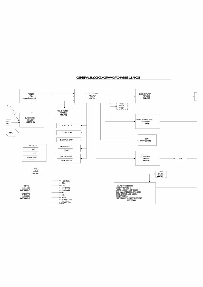
TUNERPLL
(channel/frequency)
VIDEO PROCESSORTDA 888X H
(BOCMA)(PHILIPS)
RGB AMPLIFIERTDA 6108(PHILIPS)
TV TEXT PROSDA 555X(SIEMENS)
COMB FILTERTDA 9181(PHILIPS)
IR
KEYPAD
VERTICAL AMPLIFIERSTV 9379FA
(ST)
E/WCORRECTION
HORIZONTALOUTPUTBU 2508
FBT
FRONT AV IN
BACK AV IN/OUT
SCART 1 (FULL)------------------------------
SCART 2
FRONTSVHS IN-------------------------------
BACK SVHS IN
PAUSE TV-------------------------------
PIP-------------------------------
DVD-------------------------------
INTERNET TV-------------------------------
SMPSMC 44608
(MOTOROLA)+
ACTIVE PFCMC 33260
(MOTOROLA)
SOUND PROCESSOR DOLBY (MSP 3452 G) VIRTUAL DOLBY (MSP 3411G) G/S NICAM STEREO (MSP 3410 G) BTSC STEREO (MSP 3430G) DOLBY DIGITAL (MSP 4450G,DPL 4519G,MAS 3528E) MICRONAS
VIDEOSWITCHTEA 6415
(ST)
150V/160V
+3.3V+3.3V (ST-BY)
+8V+5V
-14V(audio)+14V(audio)
GENERAL BLOCK DIAGRAM OF CHASSIS 11 AK 33
+2.5V(ST-BY)
+14V+22V
REALTIMER
PCF8583(PHILIPS)
HEADPHONE
TDA1308(PHILIPS)
OPTIC/COAX IN
EPG
+12