Embed Size (px)
Citation preview
Contents 5. On-chip Bus ............................................................. 5-1
5.1. 實驗目的 .......................................................................................5-1 5.2. 實驗原理 .......................................................................................5-1
5.2.1. Overview of the AMBA specification.................................5-1 5.2.2. Introducing the AMBA AHB ..............................................5-2 5.2.3. AMBA AHB signal list .......................................................5-3 5.2.4. The ARM-based system overview....................................5-6
5.3. 引導實驗 .......................................................................................5-8 5.3.1. 實驗步驟 .........................................................................5-11
5.4. 實驗要求 .....................................................................................5-17 5.5. 問題與討論 ..................................................................................5-17 5.6. 參考文件及網頁...........................................................................5-18

On-Chip Bus
SOC Lab Material 5-1
5. On-chip Bus
5.1. 實驗目的
To introduce the interface design conceptually. Study the communication between FPGA on logic module and ARM processor on core module. We will introduce the ARM bus in detail.
5.2. 實驗原理
5.2.1. Overview of the AMBA specification
The Advanced Microcontroller Bus Architecture (AMBA) specification defines an on-chip communications standard for designing high-performance embedded microcontrollers. Three distinct buses are defined within the AMBA specification:
The Advanced High-performance Bus (AHB) The Advanced System Bus (ASB) The Advanced Peripheral Bus (APB).
AMBA AHB implements the features required for high-performance, high clock frequency systems including:
burst transfers split transactions single-cycle bus master handover single-clock edge operation non-tristate implementation wider data bus configurations (64/128 bits).
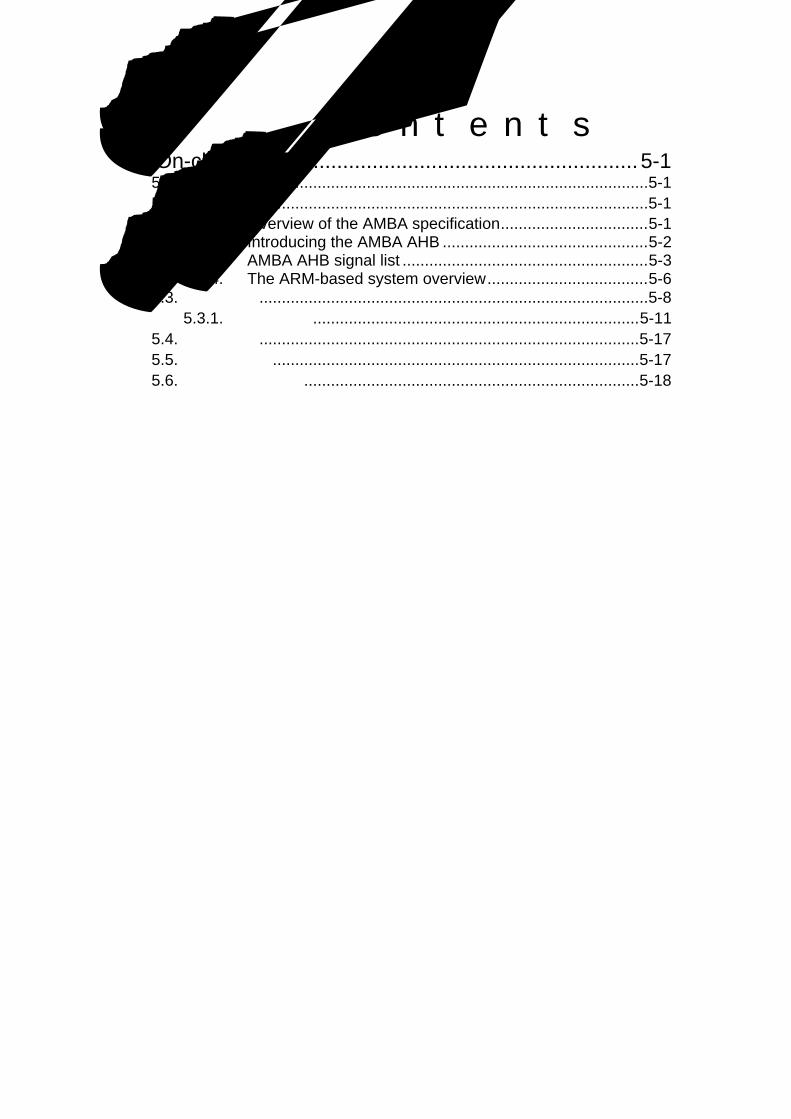
The APB is part of the AMBA hierarchy of buses and is optimized for minimal power consumption and reduced interface complexity. The AMBA APB appears as a local secondary bus that is encapsulated as a single AHB or ASB slave device. APB provides a low-power extension to the system bus which builds on AHB or ASB signals directly. We show the typical AMBA system in Figure 1
On-chip Bus
SOC Lab Material 5-2
Figure 1 A typical AMBA system
5.2.2. Introducing the AMBA AHB
A typical AMBA AHB system design contains the following components: • AHB master A bus master is able to initiate read and write operations by providing an address and control information. Only one bus master is allowed to actively use the bus at any one time. • AHB slave A bus slave responds to a read or write operation within a given address-space range. The bus slave signals back to the active master the success, failure or waiting of the data transfer. • AHB arbiter The bus arbiter ensures that only one bus master at a time is allowed to initiate data transfers. Even though the arbitration protocol is fixed, any arbitration algorithm, such as highest priority or fair access can be implemented depending on the application requirements. An AHB would include only one arbiter, although this would be trivial in single bus master systems. • AHB decoder The AHB decoder is used to decode the address of each transfer and provide a select signal for the slave that is involved in the transfer. A single centralized decoder is required in all AHB implementations. We only introduce AHB in detail here. If you have any interested in studying ASB and APB, you can refer to ARM standard.

On-Chip Bus
SOC Lab Material 5-3
5.2.3. AMBA AHB signal list
This section contains an overview of the AMBA AHB signals (see Table 1). A full description of each of the signals can be found in later sections of this document. All signals are prefixed with the letter H, ensuring that the AHB signals are differentiated from other similarly named signals in a system design.
Table 1 AMBA AHB signals Name Source Description HCLK Clock source This clock times all bus transfers. Bus clock All signal timings are related to the
rising edge of HCLK. HRESETn Reset controller Reset controller The bus reset Reset signal is active LOW and is used to
reset the system and the bus. This is the only active LOW signal.
HADDR[31:0] Master The 32-bit system address bus. Address bus HTRANS[1:0] Master Indicates the type of the current Transfer type transfer, which can be
NONSEQUENTIAL, SEQUENTIAL, IDLE or BUSY.
HWRITE Master When HIGH this signal indicates a Transfer direction write transfer and when LOW a read
transfer. HSIZE[2:0] Master Indicates the size of the transfer, Transfer size which is typically byte (8-bit),
halfword (16-bit) or word (32-bit). The protocol allows for larger transfer sizes up to a maximum of 1024 bits.
HBURST[2:0] Master Indicates if the transfer forms part a Burst type burst. Four, eight and sixteen beat
bursts are supported and the burst may be either incrementing or wrapping.
HPROT[3:0] Master The protection control signals Protection control provide additional information about
a bus access and are primarily intended for use by any module that wishes to implement some level of protection. The signals indicate if the transfer is an opcode fetch or data access, as well as if the transfer is aprivileged mode access or user mode access. For bus masters with a memory management unit thesesignals also indicate whether the current access is cacheable or bufferable.
HWDATA[31:0] Master The write data bus is used to Write data bus transfer data from the master to the
bus slaves during write operations.A minimum data bus width of 32 bits

On-chip Bus
SOC Lab Material 5-4
is recommended. However, this may easily be extended to allow forhigher bandwidth operation.
HSELx Decoder Each AHB slave has its own slave Slave select select signal and this signal indicates
that the current transfer is intended for the selected slave. This signal is
simply a combinatorial decode of the address bus.
HRDATA[31:0] Slave The read data bus is used to transferRead data bus data from bus slaves to the bus
master during read operations. A minimum data bus width of 32 bits is recommended. However, this may easily be extended to allow for higher bandwidth operation.
HREADY Slave When HIGH the HREADY signal Transfer done indicates that a transfer has finished
on the bus. This signal may bedriven LOW to extend a transfer.Note: Slaves on the bus require HREADY as both an input and an output signal.
HRESP[1:0] Slave The transfer response provides Transfer response additional information on the status of
a transfer. Four different responses are provided, OKAY, ERROR, RETRY and SPLIT.
On-Chip Bus
SOC Lab Material 5-5
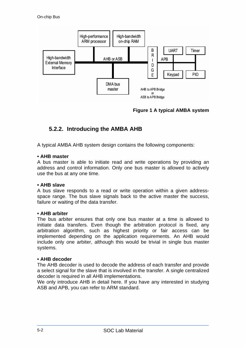
AMBA AHB also has a number of signals required to support multiple bus master operation (see Table 2). Many of these arbitration signals are dedicated point to point links and in Table 2 the suffix x indicates the signal is from module X. For example there will be a number of HBUSREQx signals in a system, such as HBUSREQarm, HBUSREQdma and HBUSREQtic.
Table 2 Arbitration signals
Name Source Description HBUSREQx Master A signal from bus master x to the Bus request bus arbiter which indicates that the
bus master requires the bus. There is an HBUSREQx signal for each bus master in the system, up to a maximum of 16 bus masters.
HLOCKx Master When HIGH this signal indicates thatLocked transfers the master requires locked access to
the bus and no other master should be granted the bus until this signal is LOW.
HGRANTx Arbiter This signal indicates that bus masterBus grant x is currently the highest priority
master. Ownership of the address/control signals changes at the end of a transfer when HREADY is HIGH, so a master gets access tothe bus when both HREADY and HGRANTx are HIGH.
HMASTER[3:0] Arbiter These signals from the arbiter Master number indicate which bus master is
currently performing a transfer and is used by the slaves which support SPLIT transfers to determine which master is attempting an access. The timing of HMASTER is aligned with the timing of the address and control signals.
HMASTLOCK Arbiter Indicates that the current master is Locked sequence performing a locked sequence of
transfers. This signal has the same timing as the HMASTER signal.
HSPLITx[15:0] Slave(SPILIT capable) This 16-bit split bus is used by a Split completion request slave to indicate to the arbiter which
bus masters should be allowed to re-attempt a split transaction. Each bit of this split bus corresponds to a single bus master.
On-chip Bus
SOC Lab Material 5-6
5.2.4. The ARM-based system overview
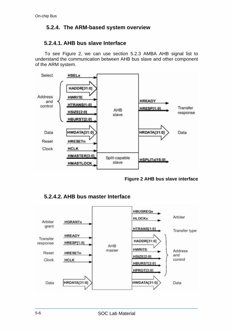
5.2.4.1. AHB bus slave Interface
To see Figure 2, we can use section 5.2.3 AMBA AHB signal list to understand the communication between AHB bus slave and other component of the ARM system.
Figure 2 AHB bus slave interface
5.2.4.2. AHB bus master Interface

On-Chip Bus
SOC Lab Material 5-7
Figure 3 AHB bus master interface
5.2.4.3. The AHB Arbiter Interface
Figure 4 AHB arbiter interface diagram
5.2.4.4. The AHB Decoder Interface
Figure 5 AHB decoder interface diagram

On-chip Bus
SOC Lab Material 5-8
Figure 6 A typical address decoding system and the slave select signals
If we want to add our design, we can download our HDL code into the FPGA. We can think that it is a ARM bus slave in the Arm-based system. In our experiment, we will explain how to add our design in detail.
5.3. 引導實驗
This program does the following tasks: 1. Determines DRAM size on the core module and sets up the system
controller. 2. Checks that the logic module is present in the AP expansion position. 3. Reports module information. 4. Sets the logic module clock frequencies. 5. Tests SSRAM for word, halfword, and byte accesses. 6. Flashe the LEDs. 7. Remains in a loop that displays the switch values on the LEDs.
We can divide our program into two parts: software and hardware 1. Software:
There are four source files in software: (1) logic.c: The main C code, Do above description. (2) logic.h: Defines, Structures, Routines used & defined in the logic
demo program. (3) platform.h: Integrator address map. (4) rw_support.s: Assembler functions for SSRAM testing.
2. Hardware:

On-Chip Bus
SOC Lab Material 5-9
Table 3 is the Hardware description
Table 3 Hardware description
File Description ASBAHBTop AHBAHBTop
These files are the top-level HDL that instantiate all of the high-speed peripherals , decoder , and all necessary support and glue logic to make a working system . The files are named so that , for example , ASBAHBTop.v is the top level for AHB peripherals connected to an ASB system bus
ASB2AHB
This is the bridge required to connect AHB peripherals to an ASB integrator system
AHBDecoder
The decoder block provides the high-speed peripherals with select lines. These are generated from the address lines and the module ID (position in stack) signals from the motherboard. The decoder blocks also contain the default slave peripheral to simplify the example structure. The integrator family of boards uses a distributed address decoding system
AHBMuxS2M
This is the AHB multiplexor that connects the read data buses from all of the slaves to the AHB masters(s)
AHBZBTRAM
High-speed peripherals require that SSRAM controller block supports Word, halfword, and byte operations to the SSRAM on the logic module
AHB2APB
This is the bridge blocks required to connect APB peripherals the high-speed AMBA AHB bus. They produce the peripheral select signals for each of the APB peripherals.
AHBAPBSys
The components required for an APB system are instantiated in this block. These include the bridge and the APB peripherals. This file also multiplexes the APB peripheral read buses and concatenates the interrupt sources to feed into the interrupt controller peripheral
APBRegs
The AOB register peripheral provides memory mapped registers that you can use to : Configure the two clock generators Write to the user LEDs Read the user switch inputs. It also latches the pressing of the push button to generate an expansion interrupt
APBlntcon
The APB interrupt controller contains all of the standard interrupt controller registers and has an input port for four APB interrupts. Four software interrupts are implemented
This program only tells us a concept how to use the ARM processor on CM to communicate with the FPGA on LM. And if we want to add our implementation, you can refer to Figure 7.

On-chip Bus
SOC Lab Material 5-10
Figure 7 The file structure
Logic module Memory map
Core SDRAM Other Modules
AHB
AHBAHBTop
AHBDecoder
AHBMuxS2M AHBZBTRAM
ZBTSRAM
MYIPAHBAHB2APB
APBlntcon APB
AHBAPBSys
APBRegs
On-Chip Bus
SOC Lab Material 5-11
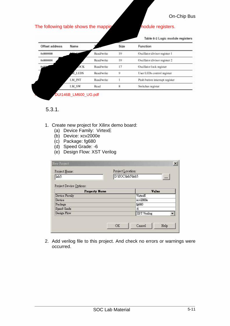
The following table shows the mapping of the logic module registers.
Reference: DUI146B_LM600_UG.pdf
5.3.1. 實驗步驟
1. Create new project for Xilinx demo board: (a) Device Family: VirtexE (b) Device: xcv2000e (c) Package: fg680 (d) Speed Grade: -6 (e) Design Flow: XST Verilog
2. Add verilog file to this project. And check no errors or warnings were occurred.
On-chip Bus
SOC Lab Material 5-12
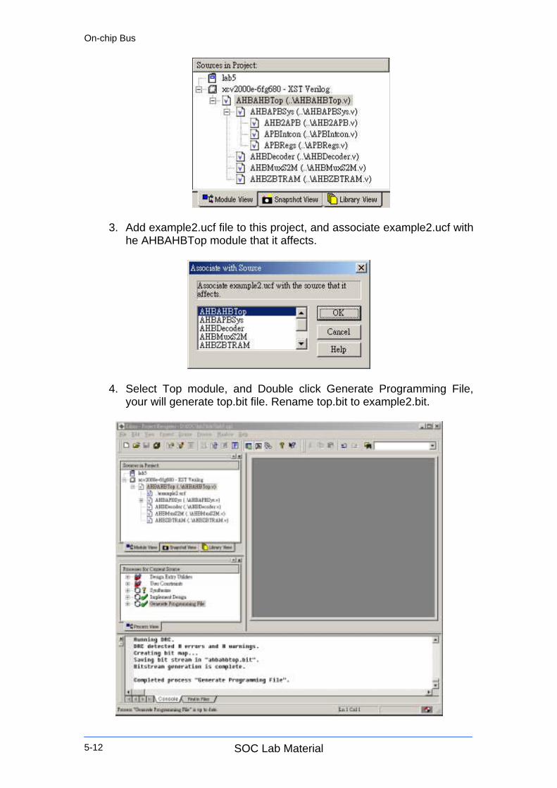
3. Add example2.ucf file to this project, and associate example2.ucf with he AHBAHBTop module that it affects.
4. Select Top module, and Double click Generate Programming File, your will generate top.bit file. Rename top.bit to example2.bit.

On-Chip Bus
SOC Lab Material 5-13
5. Copy example2.bit file to progcrd.exe directory from your project
folder. Download flow
1. Connect ARM MultiICE onto LM. (Be SURE to power down first!! …$$)
2. Set the LM in Config Mode by shorting the CFGLNK jumper on the LM board. The CFGLED on the LM is lit as an indication for configure mode. LM’s FPGA can only be detected by MultiICE Server in configure mode. Yet CM cannot be found by MultiICE Server while LM is in configure mode.
CFGLNK(J11)
3. Auto-config again in the MultiICE Server program. Remember to auto-
configure again each time the MultiICE link is modified.
4. Execute progcards.exe to download the bitstream to the FPGA. This download program only searches for the .brd files in the same directory. If only one .brd file exists, the downloading would start directly without any prompt.
5. Download the hardware binary code on FPGA. The hardware binary
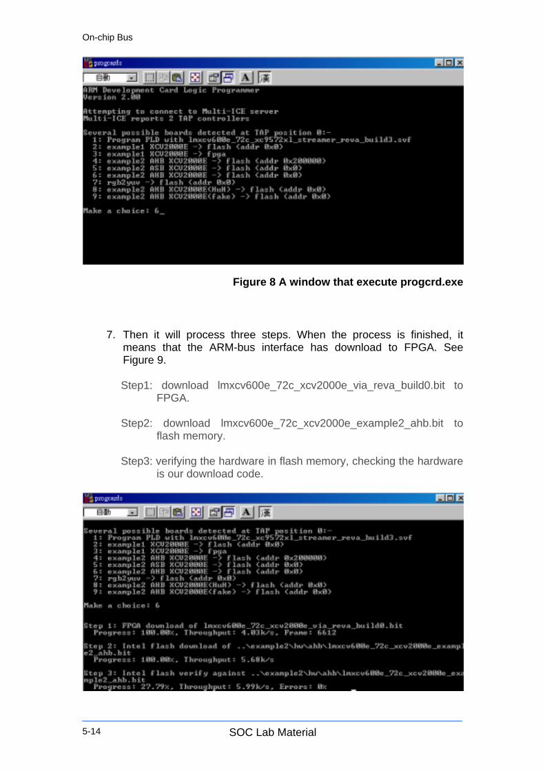
code (*.bit) can synthesize by EDA tools like Altera or Xilinx. 6. Execute the progcrd.exe, it will open a window like Figure 8. Choice 6
On-chip Bus
SOC Lab Material 5-14
Figure 8 A window that execute progcrd.exe
7. Then it will process three steps. When the process is finished, it
means that the ARM-bus interface has download to FPGA. See Figure 9. Step1: download lmxcv600e_72c_xcv2000e_via_reva_build0.bit to
FPGA.
Step2: download lmxcv600e_72c_xcv2000e_example2_ahb.bit to flash memory.
Step3: verifying the hardware in flash memory, checking the hardware is our download code.
On-Chip Bus
SOC Lab Material 5-15
Figure 9 ARM bus interface download to FPGA
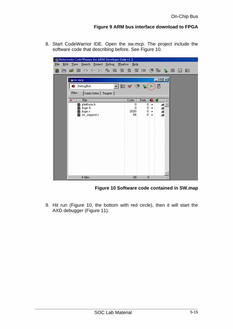
8. Start CodeWarrior IDE. Open the sw.mcp. The project include the software code that describing before. See Figure 10.
Figure 10 Software code contained in SW.map
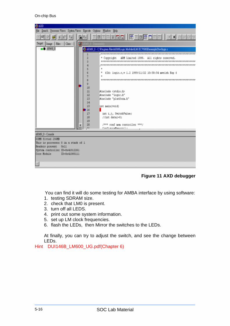
9. Hit run (Figure 10, the bottom with red circle), then it will start the AXD debugger (Figure 11).
On-chip Bus
SOC Lab Material 5-16
Figure 11 AXD debugger
You can find it will do some testing for AMBA interface by using software: 1. testing SDRAM size. 2. check that LM0 is present. 3. turn off all LEDS. 4. print out some system information. 5. set up LM clock frequencies. 6. flash the LEDs, then Mirror the switches to the LEDs. At finally, you can try to adjust the switch, and see the change between LEDs.
Hint:DUI146B_LM600_UG.pdf(Chapter 6)

On-Chip Bus
SOC Lab Material 5-17
5.4. 實驗要求
To trace the hardware code and software code, indicate that software how to communicate with hardware using the AMBA interface. Note: Clock control assignment 1. Before writing to the oscillator registers, you must unlock them by writing
the value 0x0000A05F to the LM_LOCK register. After writing the oscillator register, relock them by writing any value other than 0x0000A05F to the LM_LOCK register.
2. SRVMhzfrequence
⋅++
=)2]0:6[(
)8]0:8[(48
where
5.5. 問題與討論
1. If we want to design an accumulator (1, 2, 3…), how could you do to implement it using the scratch code?
2. If we want to design a hardware using FPGA, how could you do to add your code to the scratch code and debugger it?

On-chip Bus
SOC Lab Material 5-18
3. To study the AMBA bus standard, try to design a simple AMBA interface.
5.6. 參考文件及網頁
AMBA AHB standard 2.0. INTERGRATOR/LM-XCV600E+INTERGRATOR/LM-EP20K600E+ USER GUIDE.
INTERGRATOR/AP USER GUIDE INTERGRATOR/CM9xOT INTERGRATOR/CM7xOT USER GUIDE


![IEEE TRANSACTIONS ON VERY LARGE SCALE INTEGRATION …chengkok/papers/2007/p69... · 2009. 7. 9. · overview of SoC bus architectures is available in [4]. The main problem of shared-bus](https://img.pdfslide.net/doc/110x75/608f0bc9349a7028d905a2c8/ieee-transactions-on-very-large-scale-integration-chengkokpapers2007p69.jpg)