Embed Size (px)
Citation preview
0
iNEMI Workshop, October 22, 2013
iNEMI Workshop, October 22, 2013
Low Transmission Loss Multilayer
PWB Materials for High-Speed
and High-Frequency Applications
Kazutoshi Danjobara
Hitachi Chemical Co., Ltd.
Printed Wiring Board Materials R&D Dept.
Advanced Core Materials Business Sector
Advanced Performance Materials Operational Headquaters

1
iNEMI Workshop, October 22, 2013
Introduction
Evaluation technologies of high-frequency performance by Hitachi Chemical
Properties of new mid-loss PWB material
Innovative ultra-low loss PWB material / Target & Technical concept
/ Features & Advantages
Conclusions
Outline

2
iNEMI Workshop, October 22, 2013
Introduction
Evaluation technologies of high-frequency performance by Hitachi Chemical
Properties of new mid-loss PWB material
Innovative ultra-low loss PWB material / Target & Technical concept
/ Features & Advantages
Conclusions
Outline

3
iNEMI Workshop, October 22, 2013
Background ; Trend of transmission rate
1P
100T
10T
1T
100G
10G
1G
100M
Throughput of equipment ≒ Double / 2 years
(Predicted from telecommunication traffic)
'96 '98 '00 '02 '04 '06 '08 '10 '12 '14 '16 '18 '20
Transmission rate of PWBs / Link≒Double / 3years)
Applications
Standardization
25 Gbps /link ('14-'15)
Signal speed on PWBs is increasing year by year to meet the needs of large-volume data transmission.
■ Higher performance of communication on network platform

4
iNEMI Workshop, October 22, 2013
Transmission rate vs. trace length on PWBs
10-3 10-2 10-1 1 10 102
50
10
1
Tra
nsm
issio
n r
ate
(G
bp
s /
lin
k)
Electrical field
LSI
BGA, CSP
MCM (SiP)
-
-
-
-
-
-
- - - - - - -
Next generation transmission technology (25 Gbps / link)
⇒ Electrical ? or Optical ? or Both
Need of the lower loss PWB material is increasing for the next generation electrical transmission.
Trace length on PWBs (m)
Optical field
Optical fiber-cable
Cabinet to Cabinet
Backplane (Mid-plane)
Boundary of electrical / Optical
Daughter
Board

5
iNEMI Workshop, October 22, 2013
Requirement for High-frequency PWB material
Reduction of ad ⇒ Low Dk & Df Resin technology
Reduction of ac ⇒ High adhesion technology between resin and conductor with very low surface roughness
< Solution to lowering transmission loss >
Transmission loss (α) ≒ Dielectric loss (αd) + Conductor loss (αc)
Dk : dielectric constant, Df : Dissipation factor
f : Frequency, c : Light velocity
Rs : Surface resistance of conductor
ρ : Resistivity of conductor, b : Dielectric thickness
w : Conductor width, t : Conductor thickness
αd ∝ 27.3 × × Dk × Df f
c
αc ∝ Rs ( f , ρ,・・・) × Dk × (t, w, b,) ・・・
αd αc
t b w

6
iNEMI Workshop, October 22, 2013
Introduction
Evaluation technologies of high-frequency performance by Hitachi Chemical
Properties of new mid-loss PWB material
Innovative ultra-low loss PWB material / Target & Technical concept
/ Features & Advantages
Conclusions
Outline

7
iNEMI Workshop, October 22, 2013
Evaluation technologies of high-frequency PWBs
Parallel plate capacitance
Whispering-gallery mode(WG)
Short pulse propagation(SPP) Strip-line resonator(JPCA-TM001)
Cavity resonator perturbation
Dk & Df
10-3 10 20 30 40 50 100 1 Frequency [GHz]
(1) Dielectric properties of materials (without conductor)
(2) Practical electrical properties of PWBs (containing conductor)
Under planning
Under planning
Strip line(SL)
Micro strip-line(MSL) Transmission loss
Split post dielectric resonator(SPDR)
10-3 10 20 30 40 50 100 1 Frequency [GHz]
■ Hitachi Chemical can satisfy various evaluation requirements of high-frequency performance of materials & PWBs (e.g. Frequency bands, Form of specimen, Environmental test, etc.)
Dk & Df

8
iNEMI Workshop, October 22, 2013
Evaluation of PWB (SL & MSL)
Strip・line(SL) structure
Micro strip・line(MSL) structure
SMA connector type
(up to 20 GHz)
Probe type
(up to 40 GHz)
Test board (SL)
Various high-frequency properties of PWBs can be evaluated.
Connector available Probe
available
e.g.) High Tg material
for PKG substrate
PTFE material
Initial
After treatment
(85 ℃/85 %RH) Test board (MSL)
Measurement system V-NA & Probe station
S21
S11
Low Df material (FX-2)
9
iNEMI Workshop, October 22, 2013
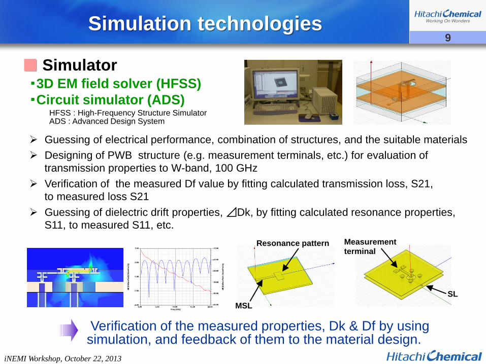
Simulation technologies
・3D EM field solver (HFSS)
・Circuit simulator (ADS)
■ Simulator
Guessing of electrical performance, combination of structures, and the suitable materials
Designing of PWB structure (e.g. measurement terminals, etc.) for evaluation of
transmission properties to W-band, 100 GHz
Verification of the measured Df value by fitting calculated transmission loss, S21,
to measured loss S21
Guessing of dielectric drift properties, ⊿Dk, by fitting calculated resonance properties,
S11, to measured S11, etc.
ADS : Advanced Design System HFSS : High-Frequency Structure Simulator
SL
Measurement terminal
MSL
Resonance pattern
Verification of the measured properties, Dk & Df by using simulation, and feedback of them to the material design.

10
iNEMI Workshop, October 22, 2013
Introduction
Evaluation technologies of high-frequency performance by Hitachi Chemical
Properties of new mid-loss PWB material
Innovative ultra-low loss PWB material / Target & Technical concept
/ Features & Advantages
Conclusions
Outline

11
iNEMI Workshop, October 22, 2013
HC's High-layer & High-frequency
materials line-up
Mid-loss material, HE-679G(S), and ultra-low loss material, LW-900G / 910G have been newly developed.
0
0.005
0.010
0.015
0.020
0.025
0.030
Dk (10 GHz) D
f (1
0 G
Hz)
4.5 4.0 3.5 3.0
HE-679G
High-Tg FR-4 (E-679)
Conventional FR-4 (E-67)
High-Tg & Low-CTE FR-4 (E-679FJ)
New mid-loss material HE-679G(S)
FX-2
Standard grade
Mid.-loss grade
Low loss grade
Ultra-low loss grade
New ultra-low loss material LW-900G/910G

12
iNEMI Workshop, October 22, 2013
Laminate properties of new mid-loss material
Item New mid-loss
HE-679G(S)
Current
HE-679G
High-Tg
FR-4
Conventional
FR-4
Glass type E E E E
Source of flame retardant Halogen free Halogen free Halogen Halogen
Dk (JPCA-TM001) 1 GHz
10 GHz
3.70-3.80
3.65-3.75
4.00
3.95
4.20
4.15
4.05
3.98
Df (JPCA-TM001) 1 GHz
10 GHz
0.0065-0.0070
0.0085-0.0090
0.0095
0.0120
0.0220
0.0250
0.0195
0.0215
Copper peel strength
(kN/m, 1/2 oz)
Standard
RTF
0.90
0.60
0.90
0.60
1.2
-
1.8
-
Tg (℃) TMA 185 185 180 125
CTE(ppm/℃)
XY
Z(α1)
Z(α2)
14
40
230
14
40
220
15
55
260
15
60
260
Solder heat resistance 288 ℃ > 300 s > 300 s > 300 s > 300 s
T-300 TMA > 60 min 30 min <10 min <5 min
Flammability UL-94 V-0 V-0 V-0 V-0
Reliability(CAF, IST, etc.) Good Good Low NG
Dk & Df of the newly developed mid-loss material, HE-679G(S), have been enhanced by maintaining the other properties as HE-679G.
13
iNEMI Workshop, October 22, 2013
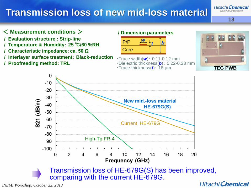
Transmission loss of new mid-loss material
< Measurement conditions >
/ Evaluation structure : Strip-line
/ Temperature & Humidity: 25 ℃/60 %RH
/ Characteristic impedance:ca. 50 Ω
/ Interlayer surface treatment: Black-reduction
/ Proofreading method: TRL
w b t
・Trace width(w): 0.11-0.12 mm ・Dielectric thickness(b): 0.22-0.23 mm ・Trace thickness(t): 18 μm
/ Dimension parameters
Core
P/P
TEG PWB
Transmission loss of HE-679G(S) has been improved, comparing with the current HE-679G.
Current HE-679G
New mid.-loss material
HE-679G(S)
High-Tg FR-4
14
iNEMI Workshop, October 22, 2013
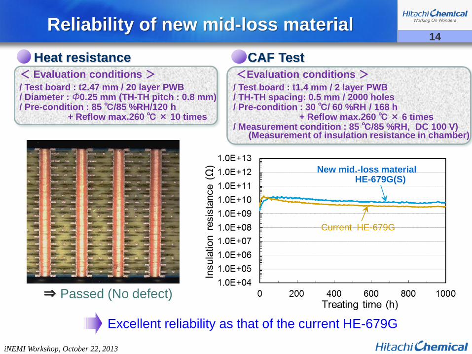
Reliability of new mid-loss material
Heat resistance
< Evaluation conditions >
/ Test board : t2.47 mm / 20 layer PWB / Diameter : Φ0.25 mm (TH-TH pitch : 0.8 mm) / Pre-condition : 85 ℃/85 %RH/120 h + Reflow max.260 ℃ × 10 times
⇒ Passed (No defect)
CAF Test
<Evaluation conditions >
/ Test board : t1.4 mm / 2 layer PWB / TH-TH spacing: 0.5 mm / 2000 holes / Pre-condition : 30 ℃/ 60 %RH / 168 h + Reflow max.260 ℃ × 6 times / Measurement condition : 85 ℃/85 %RH, DC 100 V) (Measurement of insulation resistance in chamber)
Excellent reliability as that of the current HE-679G
Current HE-679G
New mid.-loss material HE-679G(S)

15
iNEMI Workshop, October 22, 2013
Introduction
Evaluation technologies of high-frequency performance by Hitachi Chemical
Properties of new mid-loss PWB material
Innovative ultra-low loss PWB material / Target & Technical concept
/ Features & Advantages
Conclusions
Outline

16
iNEMI Workshop, October 22, 2013
E-679 LX-67Y
HE-679G
FX-2
E-67(Conventional FR-4)
E-679FJ
LZ-71G
BE-67G(H)
E-75G
New Target
PTFE laminate
Target properties of
new ultra-low loss material
High-frequency performance
HF-Performance vs. Reliability(Heat-resistance, CAF, IST, ・・・)
Grade Standard Mid-loss Low loss Ultra-low loss
(Df@10 GHz) (>0.02) (0.01-0.02) (0.005-0.01) (Df:<0.005)
Hig
h-l
ayer
relia
bilit
y
Target of new ultra low loss material is the compatibility of high-frequency performance & reliability of high-layer PWBs.

17
iNEMI Workshop, October 22, 2013
Concept & target applications of new ultra-low loss material
Target applications
& requirement
High-frequency performance
Reliability &
Process-ability
Halogen free
RF / Wireless
(Antenna, RF-modules, etc.)
・High frequency performance
・Dk & Df drift stability
(Temperature, Humidity)
High-speed PKG
(MMIC-PKG, OEIC-PKG, etc.)
Development concept
・High frequency performance
・High heat resistance
・High reliability(Low-CTE,CAF, etc)
・Halogen free
High-speed Digital / High-layer
(Servers, Routers, HPC, etc.)
・High frequency performance
・High heat resistance
・High reliability(Low-CTE,CAF, etc)

18
iNEMI Workshop, October 22, 2013
Technical composition of novel resin system designed for new ultra-low loss material
●Low CTE ●Low Df ●High heat resistance ●Low water absorption
Rigid thermosetting resin
●Low Df ●High Tg ●Low CTE ●High elastic modulus ●High heat resistance ●High flame retardancy
Reactive low polar polymer
●Low Dk & low Df ●High Tg
●Low water absorption
●High toughness
●High adhesion
Polymer-blend modification technology
with co-crosslinking reaction
Inorganic filler
Composing technology (Organic / Inorganic)
by controlling interface between resin and filler
New material has been designed by using both the resin-modification technology & filler-composition technology.

19
iNEMI Workshop, October 22, 2013
Filler / Resin - composing technology
The control of interface between resin and filler is important to enhance various properties.
Optimum
Exfoliation mode on Cu-peeling test
Optimum (FICS)
■ Example of importance of FICS
Matrix resin
Inorganic
Filler
Filler interface control system (FICS)
Optimization of interface(Filler / Resin)
⇒ Excellent adhesion & dispersion
/ Low water absorption / High peel strength / Excellent heat resistance / Excellent CAF restraining property
Conventional
Aggregation
None
→
→
Exfoliation between filler & resin
Cohesive failure of resin

20
iNEMI Workshop, October 22, 2013
Laminate properties of new ultra-low loss
material
Item New ultra-low loss Current low loss
FX-2 HE-679G
Standard
PTFE laminate LW-900G LW-910G
Resin system Thermosetting Thermosetting Thermosetting Thermoplastic
Glass type E Low Dk E E E
Source of flame retardant Halogen free Halogen Halogen free -
Dk (JPCA-TM001) 10 GHz 3.57 3.32 3.45 3.95 2.62
Df (JPCA-TM001) 10 GHz 0.0048*1) 0.0038*1)
0.0034*2) 0.0058 0.0120 0.0038
Copper peel strength
(kN/m, 1/2 oz)
RTF
HVLP
0.75
0.63
0.75
0.63
0.60
-
0.60
-
1.2(Std.-foil)
-
Tg (℃) TMA 198 198 185 185 30
CTE(ppm/℃)
XY
Z(α1)
Z(α2)
13
40
250
13
40
250
15
47
110
14
40
220
18
105
310
Solder heat resistance 288 ℃ > 300 s > 300 s > 300 s > 300 s > 300 s
T-300 TMA > 60 min > 60 min > 60 min 20 min -
Flammability UL-94 (V-0) (V-0) V-0 V-0 V-0
Reliability(CAF, IST, etc.) On internal
evaluation
On internal
evaluation
On evaluation
by PWB maker Good -
*1) Practical value calculated by the condition of strip-line structure with Cu-foil(RTF , Rz≒3 μm)
*2) Practical value calculated by the condition of strip-line structure with Cu-foil(HVLP, Rz≒1.5 μm)
21
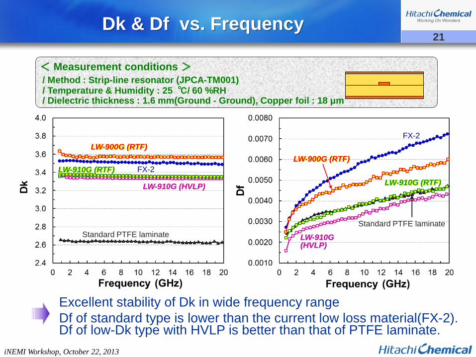
iNEMI Workshop, October 22, 2013
Dk & Df vs. Frequency
< Measurement conditions >
/ Method : Strip-line resonator (JPCA-TM001) / Temperature & Humidity : 25 ℃/ 60 %RH / Dielectric thickness : 1.6 mm(Ground - Ground), Copper foil : 18 μm
Standard PTFE laminate
FX-2
LW-900G (RTF)
LW-910G (HVLP)
LW-910G (RTF)
Excellent stability of Dk in wide frequency range
Df of standard type is lower than the current low loss material(FX-2). Df of low-Dk type with HVLP is better than that of PTFE laminate.
FX-2
Standard PTFE laminate
LW-900G (RTF)
LW-910G (HVLP)
LW-910G (RTF)

22
iNEMI Workshop, October 22, 2013
Dk & Df vs. Temperature
< Measurement conditions >
/ Method : Strip-line resonator (JPCA-TM001) / Temperature : -25~100 ℃ / Dielectric thickness : 1.6 mm(Ground - Ground), Copper foil : 18 μm
Standard PTFE laminate
FX-2
LW-900G (RTF)
LW-910G (RTF)
Standard PTFE laminate
FX-2 LW-900G (RTF)
LW-910G (RTF)
Excellent stability against temperature change

23
iNEMI Workshop, October 22, 2013
Dk & Df vs. Moisture absorption
< Measurement conditions >
/ Method : Strip-line resonator (JPCA-TM001) / Moisture absorption treatment : 85 ℃/85 %RH/-1000 h / Dielectric thickness : 1.6 mm(Ground - Ground), Copper foil : 18 μm
Better stability against moisture absorption treatment compared with high-Tg FR-4
FX-2
LW-900G (RTF)
LW-910G (RTF)
High-Tg FR-4 High-Tg FR-4
FX-2 LW-900G (RTF)
LW-910G (RTF)

24
iNEMI Workshop, October 22, 2013
Transmission loss of
new ultra-low loss material
< Measurement conditions >
/ Evaluation structure : Strip-line
/ Temperature & Humidity: 25 ℃/60 %RH
/ Characteristic impedance:ca. 50 Ω
/ Interlayer surface treatment: Black-reduction
/ Proofreading method: TRL
w b t
・Trace width(w): 0.120 mm ・Dielectric thickness(b): 0.23-0.25 mm ・Trace thickness(t): 18 μm
/ Dimension parameters
Core
P/P
TEG PWB
HVLP(Rz≒1.5 μm)
RTF(Rz≒3 μm)
-25 dB/[email protected] GHz
-33 dB/[email protected] GHz
Improved by 8 dB/m(12.5 GHz) compared with current low loss material

25
iNEMI Workshop, October 22, 2013
Eye pattern diagrams
< Measurement conditions >
/ Evaluation PWB : Former S21 evaluation PWB(Strip-line )
/ Bit rate : 12.5 Gbps (Trace length : 300 mm) , 25 Gbps (Trace length : 100 & 300 mm)
Eye-opening of LW-900G is better than the others.
12.5 Gbps
L:300mm
25 Gbps
L:100mm
25 Gbps
L:300mm
Vo
ltag
e (m
V)
Vo
ltag
e (m
V)
Vo
ltag
e (m
V)
Vo
ltag
e (m
V)
Vo
ltag
e (m
V)
Vo
ltag
e (m
V)
Vo
ltag
e (m
V)
Vo
ltag
e (m
V)
Vo
ltag
e (m
V)
Vo
ltag
e (m
V)
Vo
ltag
e (m
V)
Vo
ltag
e (V
) Time (ps) Time (ps) Time (ps) Time (ps)
Time (ps) Time (ps) Time (ps) Time (ps)
Time (ps) Time (ps) Time (ps) Time (ps)
Item HE-679G FX-2 LW-900G(RTF) LW-910G(HVLP)

26
iNEMI Workshop, October 22, 2013
Construction of PWB (20 layers)
1 Grand 0.5oz copper foil~~~~~~~~~~ GWA-900G 1080N65
2 Grand
3 Signal~~~~~~~~~~~~~~~~~~~~
4 Grand
5 Signal~~~~~~~~~~~~~~~~~~~~
6 Grand
7 Signal~~~~~~~~~~~~~~~~~~~~
8 Grand
9 Signal~~~~~~~~~~~~~~~~~~~~
10 Grand
11 Grand~~~~~~~~~~~~~~~~~~~~
12 Signal
13 Grand~~~~~~~~~~~~~~~~~~~~
14 Signal
15 Grand~~~~~~~~~~~~~~~~~~~~
16 Signal
17 Grand~~~~~~~~~~~~~~~~~~~~
18 Signal
19 Grand~~~~~~~~~~ GWA-900G 1080N65
20 Grand 0.5oz copper foil
MCL-LW-900G 0.13mm 35D
MCL-LW-900G 0.13mm 35D
MCL-LW-900G 0.13mm 35D
MCL-LW-900G 0.13mm 35D
MCL-LW-900G 0.13mm 35D
MCL-LW-900G 0.13mm 35D
MCL-LW-900G 0.13mm 35D
GWA-900G 1080N65 x 2ply
GWA-900G 1080N65 x 2ply
GWA-900G 1080N65 x 2ply
MCL-LW-900G 0.13mm 35D
MCL-LW-900G 0.13mm 35D
GWA-900G 1080N65 x 2ply
GWA-900G 1080N65 x 2ply
GWA-900G 1080N65 x 2ply
GWA-900G 1080N65 x 2ply
GWA-900G 1080N65 x 2ply
<Test Board>
Layer Count :20 layers
PCB Thickness :2.9mm
27
iNEMI Workshop, October 22, 2013
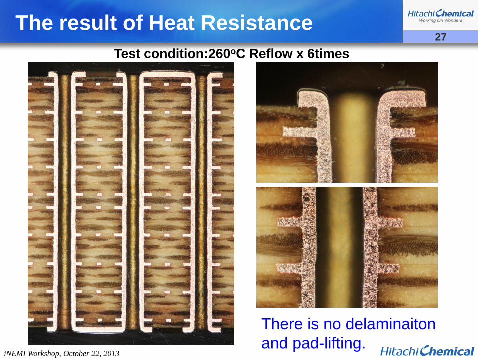
The result of Heat Resistance
Test condition:260oC Reflow x 6times
There is no delaminaiton
and pad-lifting.
28
iNEMI Workshop, October 22, 2013
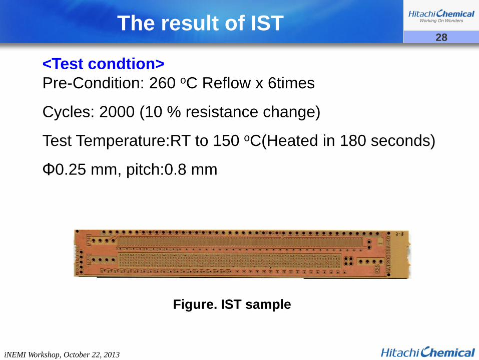
The result of IST
<Test condtion>
Pre-Condition: 260 oC Reflow x 6times
Cycles: 2000 (10 % resistance change)
Test Temperature:RT to 150 oC(Heated in 180 seconds)
Φ0.25 mm, pitch:0.8 mm
Figure. IST sample

29
iNEMI Workshop, October 22, 2013
The result of IST
<Test condtion> Pre-Condition: 260 oC Reflow x 6 times Cycles: 2000 (10 % resistance change)
Test Temperature:RT to 150 oC(Heated for 180 s), Φ0.25 mm, pitch:0.8 mm
-4
-2
0
2
4
6
8
10
121
82
163
244
325
406
487
568
649
730
811
892
973
1054
1135
1216
1297
1378
1459
1540
1621
1702
1783
1864
1945
Re
sis
nta
nce (
change in %
)
Cycles to Failure
Item pre-condition cycles result
1 - 2,000 OK
2 260oC x 6 2,000 OK
30
iNEMI Workshop, October 22, 2013
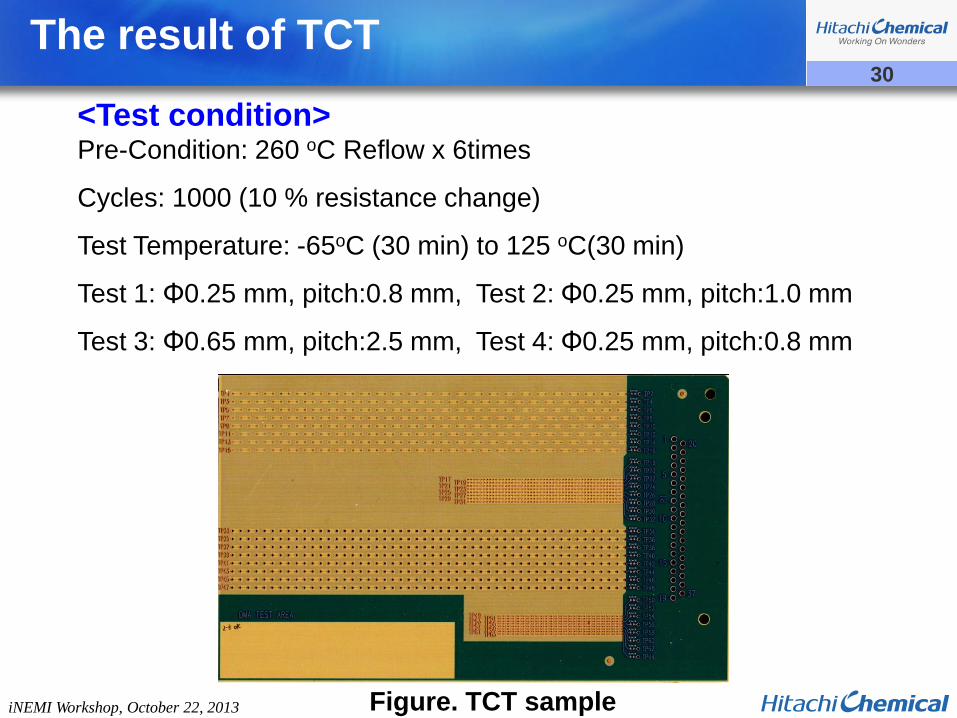
The result of TCT
<Test condition> Pre-Condition: 260 oC Reflow x 6times
Cycles: 1000 (10 % resistance change)
Test Temperature: -65oC (30 min) to 125 oC(30 min)
Test 1: Φ0.25 mm, pitch:0.8 mm, Test 2: Φ0.25 mm, pitch:1.0 mm
Test 3: Φ0.65 mm, pitch:2.5 mm, Test 4: Φ0.25 mm, pitch:0.8 mm
Figure. TCT sample

31
iNEMI Workshop, October 22, 2013
The result of TCT
-4
-2
0
2
4
6
8
10
12
0 200 400 600 800 1000
resis
tan
ce
ch
an
ge (
%)
cycles
φ0.25 mm, pitch:2.5 mm
φ0.25 mm, pitch:1.0 mm
φ0.65 mm, pitch:2.5 mm
φ0.25 mm, pitch:0.8 mm
<Test Condition>
Pre-Condition: 260 oC Reflow x 6 times
Cycles: 1000 (10 % resistance change)
Test temperature: : -65oC (30 min) to 125 oC(30 min)

32
iNEMI Workshop, October 22, 2013
Insulation reliability(CAF evaluation) (1)
Diameter:φ0.15 mm
TH - TH spacing:0.2 mm
< Evaluation conditions >
/ Evaluation board : t0.8 mm(Cu:18 μm) / 2 layer PWB / Diameter : Φ0.15 mm / TH-TH spacing : 0.2 mm / Pre-condition : 85 ℃/85 %RH/120 h + Reflow max.260 ℃ × 8 times / Measurement condition : HAST(130 ℃/85 %RH), DC 5.5 V (Continuous measurement of insulation resistance in chamber)
Excellent CAF restraining property & drilling process-ability
Crack (glass/resin) by drilling
: <10~20 μm
LW-900G
High-Tg FR-4
Conventional FR-4
HE-679G

33
iNEMI Workshop, October 22, 2013
< Board spec. >
- Board thickness: 2.0 mm
- T/H pitch: 0.8 mm, Wall-Wall distance: 0.5 mm, 2,000 holes
< Test condition >
- Precondition: 255 oC reflow x 8 times
- CAF testing: 85 oC/ 85 %RH, DC 100V
- Measurement of insulation resistance in chamber
1.0E+04
1.0E+06
1.0E+08
1.0E+10
1.0E+12
0 200 400 600 800 1000
Insu
lati
on
resis
tan
ce
(Ω)
Treating time (h)
TH-TH distance:0.5 mm
TH-TH distance:0.4 mm
Insulation reliability(CAF evaluation) (2)

34
iNEMI Workshop, October 22, 2013
■ Features of LW-900G & 910G
Features & Current status of new ultra-low loss material (LW-900G)
Df@10 GHz ⇒ E-glass type : Lower than current low loss material(FX-2)
Low-Dk type : same or better compared with PTFE material
Thermal-mechanical properties(Tg,CTE,etc) ⇒ Better than FX-2
Heat resistance ⇒ Excellent
Flame retardancy ⇒ V-0 by Halogen-free resin system
Reliability of high-layer PWB (CAF, TCT, IST, etc.) ⇒ Excellent
Drilling process-ability of high-layer PWB ⇒ On evaluation
■ Ongoing study Optimization of mass production process
Reliability test (CAF, TCT & IST) of high-layer PWB using Hybrid structure
Further improvement of dielectric properties
for the next generation material (Df Target : < 0.002@10-20 GHz)

35
iNEMI Workshop, October 22, 2013
Road Map of HC's high-frequency Materials
・Router ・Server ・Storage ・Transport ・HPC ・Measurement equipment ・IC-tester, etc.
Transmission rate/link (Backplane)
High-end digital (High-speed & High-layer)
LZ-71G Dk:3.6/Df:0.006
Middle~Std.
digital
FX-2 Dk:3.5/Df:0.003
Applications
RF/Wireless (Analog high- Freq.)
・Antenna ・Sensor ・RF-Module ・Base station ・Mobile devices
(Mobile)
HE-679G Dk:4.0/Df:0.009
3.2~6.4 Gbps ~12.5 Gbps ~25 Gbps >50Gbps
5.7 Mbps 7.2 Mbps 12 Mbps >25Mbps
Dk<3.7/Df<0.003
Dk<4.0/Df<0.01
Dk<3.5/Df<0.003
2010 2012 2014 2016 2018
Dk<3.3/Df<0.002
Dk<3.3/Df<0.002
High-speed -PKG
・PC/Server ・Mobile devices ・RF-Module ・MMIC-PKG
LZ-71G Dk:3.6/Df:0.006
E-800G Dk:4.0/Df:0.005
Dk&Df: value of 1GHz
AS-Z5 Df:0.005
HE-679G(S) Df:0.006
LW-900G Df:0.002
New Df:<0.005
Df<0.005
LW-900G Df:0.002
Df<0.01
AS-Z3(K) Df:0.013
AS-Z2 Df:0.015
Df<0.02 Df<0.015 Df<0.005 Build-up material for PKG
・PC/Server ・Mobile devices ・RF-Module ・MMIC-PKG
Dk<3.0/Df<0.001
New Df:<0.001
Dk<3.8/Df<0.007 Dk<3.6/Df<0.005
Dk<3.0/Df<0.001
FX-2/FX-3 Dk:3.2-3.5/
Df:0.0025-0.0028
LW-900G Df:0.002
New Df:<0.001
Df<0.002
New Df:<0.001
Df<0.002
New Df:<0.002

36
iNEMI Workshop, October 22, 2013
Introduction
Evaluation technologies of high-frequency performance by Hitachi Chemical
Properties of new mid-loss PWB material
Innovative ultra-low loss PWB material / Target & Technical concept
/ Features & Advantages
Conclusions
Outline

37
iNEMI Workshop, October 22, 2013
Conclusions
■ We have lined up low transmission loss PWB materials for
high-speed and high-frequency applications.
■ The new mid-loss material, HE-679G(S) has lower Dk and Df
than current material, HE-679G, and has the excellent reliability
as HE-679G.
■ Novel low loss and halogen free thermosetting resin system has
been designed for the next generation high-speed applications.
■ Innovative ultra-low loss material, LW-900G&910G with the novel
resin technology shows lower Df than standard PTFE laminate,
and is characterized by high Tg, low CTE, high heat resistance,
the excellent CAF property, and the process-ability almost similar
to FR-4.
Note: The contents of this report are based on the results of experiments
and do not represent a guarantee of the values for each property.

38
iNEMI Workshop, October 22, 2013
Thank you for your attention!