Embed Size (px)
Citation preview

8/3/2019 0TC Voltage Ref
http://slidepdf.com/reader/full/0tc-voltage-ref 1/16
1
A CMOS Voltage Reference Based on Weighted
Difference of Gate-Source Voltages between PMOS
and NMOS Transistors for Low Dropout Regulators
Ka Nang Leung and Philip K. T. Mok
Department of Electrical and Electronic Engineering
The Hong Kong University of Science and Technology

8/3/2019 0TC Voltage Ref
http://slidepdf.com/reader/full/0tc-voltage-ref 2/16
2
Outlines
• Brief Review on Conventional MOS VoltageReference Based on Threshold Voltages
• Proposed CMOS Voltage Reference
• Conclusions

8/3/2019 0TC Voltage Ref
http://slidepdf.com/reader/full/0tc-voltage-ref 3/16
3
Conventional MOS Voltage ReferenceBased on Threshold Voltages
2 th1thref V V V -
[1] B.-S. Song and P. R. Gray, “Threshold-Voltage Temperature Drift in Ion-Implanted MOS
Transistors”, IEEE Journal of Solid-State Circuits, vol. SC-17, pp. 291-298, Apr. 1982.

8/3/2019 0TC Voltage Ref
http://slidepdf.com/reader/full/0tc-voltage-ref 4/16
4
Requirements of Conventional Reference
• Good matching of TC of Vth for low-TC Vref èRequire extensive process controls
èExpensive
• Require NMOS (PMOS) transistors with different Vth
èRequire multi-threshold-voltage process or
depletion-enhancement transistor process
èNot compatible in standard CMOS process

8/3/2019 0TC Voltage Ref
http://slidepdf.com/reader/full/0tc-voltage-ref 5/16
5
General Idea of Proposed CMOS Reference
NMOS ThresholdNMOS Threshold
Voltage Generator Voltage Generator
PMOS ThresholdPMOS Threshold
Voltage Generator Voltage Generator
ScalingScaling
Factor k Factor k
S+
TempTemp
VREF VREFTempTemp
|VTHP||VTHP|
THPTHNref VkVV -
TempTemp
VTHN VTHN
Controlled by circuit
parameters

8/3/2019 0TC Voltage Ref
http://slidepdf.com/reader/full/0tc-voltage-ref 6/16
6
Core Circuit
VREF
PMOS
NMOS
R1
R2
IB
VCC
ú
úúú
û
ù
ê
êêê
ë
é
-
÷ø
ö
çè
æ
÷ø
öçè
æ
÷ø
öçè
æ+
÷ø
ö
çè
æ
ú
û
ùê
ë
é-÷
ø
öçè
æ+
-÷ø
öçè
æ+
1
L
W
L
W
R
R 1
L
W
C
I 2
V V
R
R 1
V V R
R 1V
N N
P P
2
1
P OX P
B
THP THN 2
1
)PMOS ( GS )NMOS ( GS 2
1REF
m
m
m
8/3/2019 0TC Voltage Ref
http://slidepdf.com/reader/full/0tc-voltage-ref 7/16
7
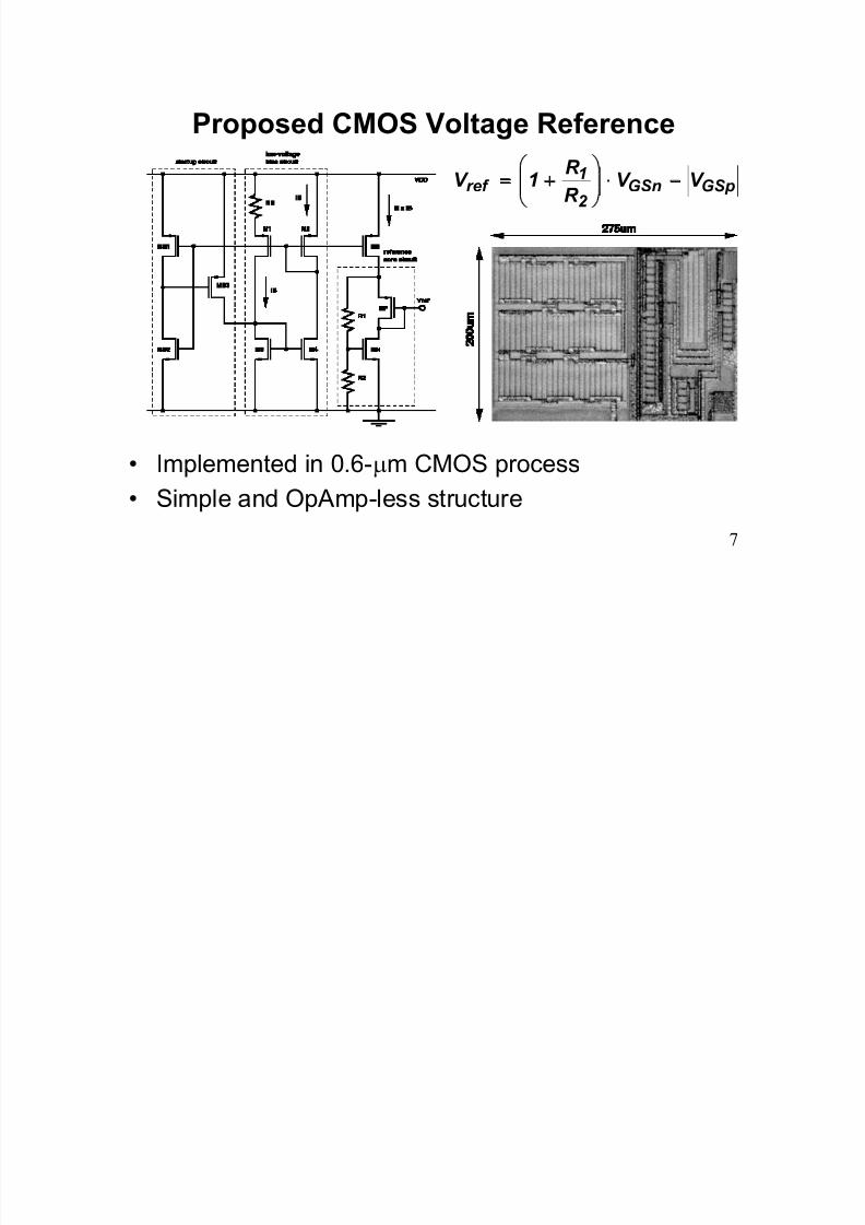
Proposed CMOS Voltage Reference
GSpGSn2
1ref V V
R
R 1V -÷
ø
öçè
æ+
• Implemented in 0.6-mm CMOS process
• Simple and OpAmp-less structure

8/3/2019 0TC Voltage Ref
http://slidepdf.com/reader/full/0tc-voltage-ref 8/16
8
Minimum Supply Voltage
)sat ( 5 DS o
GSn2
1mins V C 0 @ V
R
R 1V +÷
ø
öçè
æ+
• Vsmin = 1.4V(Vthn » |Vthp| » 0.9V@0oC)
• Sub-1-V supply
voltage is possible for
Vth < 0.6V

8/3/2019 0TC Voltage Ref
http://slidepdf.com/reader/full/0tc-voltage-ref 9/16
9
Design Considerations
)mobilitiesand current ( F )voltagethreshold ( F
T
V
T
V
R
R 1
T
V
2 1
GSpGSn
2
1ref
+
¶-
¶÷ø
öçè
æ+
linear temp dependence non-linear temp dependence
1R
R
vthn
vthp
2
1-
b
b
2
p
n2
vthn
vthp
o
r
o p
on
n
p
2 2
1
T
T
)T (
)T (
L
W
L
W n p
÷ø
ö
çè
æ+÷
ø
öçè
æ
÷ø
öçè
æ
=÷ø
öçè
æ
÷ø
öçè
æ-
m
m
b
b
b
b
b
m
mm

8/3/2019 0TC Voltage Ref
http://slidepdf.com/reader/full/0tc-voltage-ref 10/16
10
Experimental Results
With optimum resistor ratio - TC = 24 ppm/oC
312.3
312.4312.5
312.6
312.7
312.8
312.9
313.0
313.1
313.2
313.3
0 20 40 60 80 100
Temperature (degree C)
R e
f e r e n c e v o l t a g e ( m
V )
Vs = 1.40 V Vs = 2.00 V Vs = 3.00 V

8/3/2019 0TC Voltage Ref
http://slidepdf.com/reader/full/0tc-voltage-ref 11/16
11
Resistor Ratio Sensitivity
1
R
R
vthn
vthp
2
1-
b
b
Typically, 0 < R1/R2 < 1 since bvthp is close to bvthn
(~1.2 to 4 mV/K)
So, the error on the resistance ratio in the proposeddesign is better than that in bandgap reference since
2
1
2
1
2
1
2
1
R
R R
R
R
R 1
R
R
÷ø
ö
çè
æ
<<
+
÷ø
ö
çè
æ D

8/3/2019 0TC Voltage Ref
http://slidepdf.com/reader/full/0tc-voltage-ref 12/16
12
Comparison with Bandgap Reference
-100%
0%
100%
200%
300%
400%
500%
600%
1% 2% 3%
Resistor Ratio Variation
V r e
f T C
V a r
i a t i o
n
BGVEF CMOSVREF
Comparison on Resistor Ratio Variation

8/3/2019 0TC Voltage Ref
http://slidepdf.com/reader/full/0tc-voltage-ref 13/16
13
Experimental Results on Change of R Ratio
312.3
312.4
312.5
312.6
312.7
312.8
312.9
313.0
313.1
313.2
313.3
0 20 40 60 80 100
Temperature (degree C)
R e f e r e n c e v o l t a g
e ( m V )
Vs = 1.40 V Vs = 2.00 V Vs = 3.00 V
331.5
332.0
332.5
333.0
333.5
334.0
334.5
0 20 40 60 80 100
Temperature (degree C)
R e f e r e n c e v o l t a g e
( m V )
Vs = 1.40 V Vs = 2.00 V Vs = 3.00 V
With optimumresistor ratio
TC = 24 ppm/oC
Resistor ratio off by6.23%
TC = 50 ppm/oC

8/3/2019 0TC Voltage Ref
http://slidepdf.com/reader/full/0tc-voltage-ref 14/16
14
Summary of the Measurement Results
~ ±0.03%/V (typical)±0.17%/V (max)
Line regulation
~ 25 ppm/oC (typical)
62 ppm/oC (max)
TC (0 to 100 oC)302.24±12 mVReference voltage
9.7 mA (max)Supply current
1.4 to 3 VSupply voltage
Measured results of 11 samples of 2 runs

8/3/2019 0TC Voltage Ref
http://slidepdf.com/reader/full/0tc-voltage-ref 15/16
15
Applications of the Proposed Voltage Reference
• Low Supply Voltage (down to 1.5V)• True CMOS Technology
• Output Voltage is adjusted by resistor network

8/3/2019 0TC Voltage Ref
http://slidepdf.com/reader/full/0tc-voltage-ref 16/16
16
Conclusions
A CMOS Voltage Reference is proposed• Compatible and reproducible in standard CMOStechnology
• Simple and OpAmp-less structure
• Temperature dependence is controlled by circuitparameters instead of requiring extensive processcontrols
• Low sensitivity on the resistor ratio
• Small size
• Good TC performance for power converter applications