Embed Size (px)
Citation preview
8/4/2019 1-246
http://slidepdf.com/reader/full/1-246 1/11
Application Report SLAA147 - June 2002
1
Sample Code for Interfaceing the TLV320AIC1106 Codec With the TMS320C5402 DSP
Bolanle Onodipe High Precision Analog/Data Acquisition Products
ABSTRACT
The TLV320AIC1106 is one of Texas Instrument’s (TI) high-performance codecs designedfor easy use in various voice-band communication applications. This application reportprovides the user with a simple software package that facilitates the interface of this codecwith the TMS320C5402 DSP. It provides a good basis for more complex systemdevelopments. This report highlights some of the often-overlooked design issues that oneshould give consideration.
Contents
1 Introduction 2. . . . . . . . . . . . . . . . . . . . . . . . . . . . . . . . . . . . . . . . . . . . . . . . . . . . . . . . . . . . . . . . . . . . . . . . .
2 Design Concept 3. . . . . . . . . . . . . . . . . . . . . . . . . . . . . . . . . . . . . . . . . . . . . . . . . . . . . . . . . . . . . . . . . . . . .
3 Software Interface 3. . . . . . . . . . . . . . . . . . . . . . . . . . . . . . . . . . . . . . . . . . . . . . . . . . . . . . . . . . . . . . . . . . .3.1 DSP Initialization 3. . . . . . . . . . . . . . . . . . . . . . . . . . . . . . . . . . . . . . . . . . . . . . . . . . . . . . . . . . . . . . . . .3.2 DSP System Clock Frequency 3. . . . . . . . . . . . . . . . . . . . . . . . . . . . . . . . . . . . . . . . . . . . . . . . . . . . .3.3 Software Loop Control 4. . . . . . . . . . . . . . . . . . . . . . . . . . . . . . . . . . . . . . . . . . . . . . . . . . . . . . . . . . . .3.4 McBSP Initialization 5. . . . . . . . . . . . . . . . . . . . . . . . . . . . . . . . . . . . . . . . . . . . . . . . . . . . . . . . . . . . . . .3.5 Interrupts 7. . . . . . . . . . . . . . . . . . . . . . . . . . . . . . . . . . . . . . . . . . . . . . . . . . . . . . . . . . . . . . . . . . . . . . . .3.6 CPLD Register Initialization 7. . . . . . . . . . . . . . . . . . . . . . . . . . . . . . . . . . . . . . . . . . . . . . . . . . . . . . . .3.7 TLV320AIC1106 Control 9. . . . . . . . . . . . . . . . . . . . . . . . . . . . . . . . . . . . . . . . . . . . . . . . . . . . . . . . . . .3.8 Codec’s ADC/DAC Sampling Frequency 10. . . . . . . . . . . . . . . . . . . . . . . . . . . . . . . . . . . . . . . . . . . .3.9 Design Issues 10. . . . . . . . . . . . . . . . . . . . . . . . . . . . . . . . . . . . . . . . . . . . . . . . . . . . . . . . . . . . . . . . . . .
4 References 10. . . . . . . . . . . . . . . . . . . . . . . . . . . . . . . . . . . . . . . . . . . . . . . . . . . . . . . . . . . . . . . . . . . . . . . . .
List of Figures
1 TLV320AIC1106 Codec EVM 2. . . . . . . . . . . . . . . . . . . . . . . . . . . . . . . . . . . . . . . . . . . . . . . . . . . . . . . . . . . . .
2 Main Loop Control Flow Chart 5. . . . . . . . . . . . . . . . . . . . . . . . . . . . . . . . . . . . . . . . . . . . . . . . . . . . . . . . . . . .
3 CLPD Control Schematic 8. . . . . . . . . . . . . . . . . . . . . . . . . . . . . . . . . . . . . . . . . . . . . . . . . . . . . . . . . . . . . . . . .
4 13-Bit Linear Mode A/D and D/A Data Format 10. . . . . . . . . . . . . . . . . . . . . . . . . . . . . . . . . . . . . . . . . . . . .
TMC320C5402 DSP is a trademark of Texas Instruments..
Trademarks are the property of their respective owners.
8/4/2019 1-246
http://slidepdf.com/reader/full/1-246 2/11
SLAA147
2 Sample Code for Interfaceing the TLV320AIC1106 Codec With the TMS320C5402E DSP
List of Tables
1 DIP Switch Settings for CLKMD Configuration 4. . . . . . . . . . . . . . . . . . . . . . . . . . . . . . . . . . . . . . . . . . . . . .
2 McBSP Hardware Pin Description 6. . . . . . . . . . . . . . . . . . . . . . . . . . . . . . . . . . . . . . . . . . . . . . . . . . . . . . . . .
3 McBSP Registers Memory Map 6. . . . . . . . . . . . . . . . . . . . . . . . . . . . . . . . . . . . . . . . . . . . . . . . . . . . . . . . . . .
4 CLDP Control Register, CNTL2 8. . . . . . . . . . . . . . . . . . . . . . . . . . . . . . . . . . . . . . . . . . . . . . . . . . . . . . . . . . .
5 Data Conversion Format 9. . . . . . . . . . . . . . . . . . . . . . . . . . . . . . . . . . . . . . . . . . . . . . . . . . . . . . . . . . . . . . . . .
6 Functions and Default Settings of Jumpers W1 and W2 for the TLV320AIC1106EVM 9. . . . . . . . . . . .
7 Volume Control Bit Definition in Linear Mode 9. . . . . . . . . . . . . . . . . . . . . . . . . . . . . . . . . . . . . . . . . . . . . . .
1 Introduction
Texas Instruments offers a wide range of high performance codecs that can be used in variousvoice-band communication applications. The TLV320AIC1106 device is a low-power pulse codemodulation (PCM) codec designed to perform analog-to-digital (A/D) conversion (coding),digital-to-analog (D/A) conversion (decoding), and transmit and receive filtering for voice-bandsystems that meet the Consultative Committee on International Telegraphy and Telephony(CCITT) g.714 requirements. It has a pin-selectable data-formatting mode that allows operation
as a 13-bit linear device or an 8-bit companded (µ-Law) device. All internal clocks required bythe device are generated automatically from the input 2.048-MHz master clock. There is also anintegrated voice-band band pass filter whose passband ranges from 300 Hz to 3.4 kHz.
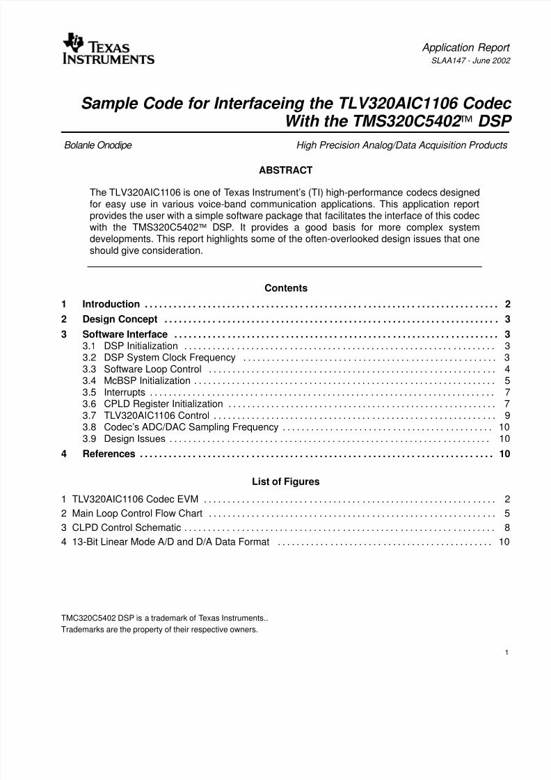
The AIC1106 is simple to interface because there are no registers to program. Only the receivevolume control can be modified. This option is only available if the 13-bit linear mode is selected.TI has introduced an inexpensive AIC1106 evaluation module (EVM), the TLV320AIC1106EVM,that is easily interfaced with a C54x DSP development platform [reference 2].
Figure 1 shows the TLV320AIC1106EVM.
2000 (mil)
2375 (mil)
1 2 5 0 ( m i l )
Figure 1. TLV320AIC1106 Codec EVM
The C5402 DSP is a fixed-point DSP with 16-K word on-chip memory and various on-chipperipherals. The C5402 DSP performs up to 100 million instructions per second (MIPS), whilethe C5402A DSP performs up to 160 MIPS. These peripherals include two multichannelbuffered serial ports (McBSP’s), an enhanced 8-bit parallel host port, two 16-bit timers, and asix-channel direct memory access (DMA) controller [reference 6]. TI also has a series of DSPstarter kits (DSK) for the various DSP families, in this case the C5402 DSK. When interfacedwith this starter kit, the DSP systems developer can design and test a complete AIC1106 codecsystem.
8/4/2019 1-246
http://slidepdf.com/reader/full/1-246 3/11
SLAA147
3Sample Code for Interfaceing the TLV320AIC1106 Codec With the TMS320C5402E DSP
This application report describes the software needed to interface the AIC1106 codec with theC54xx DSP. It also provides a tested and proven software example code.
For more information on the C5402 DSP see reference 7, and for more information on theAIC1106 codec, see references 2 and 5.
2 Design Concept
The AIC1106 codec is a voice-band communication device that interfaces easily C5402 DSKthrough the DSK’s McBSP port. See the Section 2.4 TLV320AIC1106 Control and Section 2.7 onthe McBSP initialization for detailed information on configuring both the AIC1106 codec and theMcBSP.
The codec operates as a stand-alone slave that receives all its timing and synchronizationsignals from the DSP, the master. The DSP is programmed to generate a 2.048-MHz clocksignal, and an 8-kHz frame synchronization signal. These signals are made available at theCLKX and FSX terminals of McBSP1 respectively. They both drive the MCLK and thePCMSYNC inputs of the codec. The analog-to-digital conversion output of the codec is availableat the PCMO terminal of the codec, and the digital input to the digital-to-analog converter is fedinto the codec through the PCMI terminal.
This device is a 13-bit codec with a configurable data I/O format. The data format is a 13-bit, left justified, linear data format, or an 8-bit, left justified, companded µ-law data format.
The basic concept of this example is as follows:
• Sample a given analog input signal at 8 kHz through the receive terminal of the DSP.
• Append each sampled 13-bit data with a 3-bit receiver volume gain control code, and reroutethe results to the digital-to-analog converter of the codec through the DSP’s transmitterminal.
3 Software Interface
For the interaction between the DSP and the codec, a set of software routines was developed.These include the DSP initialization routine for both the McBSP and the complex programmablelogic device (CPLD) registers and the interrupt service routines for the DSP/codec handshake.This software package is available for download, see the AIC1106.zip file in the product folder.The user can adapt this software package for whatever application they wish to implement. Inaddition, shell programs or templates for customizing application software programs are alsoavailable [see reference 4].
3.1 DSP Initialization
The DSP initialization routine sets up the DSP by programming its memory-mapped registers
(MMRs) to the top of the data-memory page. For a more comprehensive discussion of theMMRs, [see reference 6]. The MMRs are defined in the MMRegs.h file in the software packagedown load file, see the AIC1106.zip file in the product folder.
3.2 DSP System Clock Frequency
An onboard 20-MHz crystal oscillator provides the basic system clock for the C5402 DSK. Theon-chip phase locked loop (PLL) circuitry provides a series of derivative clock frequencies thatcan be selected by meeting either of the following conditions:
8/4/2019 1-246
http://slidepdf.com/reader/full/1-246 4/11
SLAA147
4 Sample Code for Interfaceing the TLV320AIC1106 Codec With the TMS320C5402E DSP
• Hardware, flipping the posts of the DIP switches DIP SW #5, DIP SW #4 and DIP SW#3 thatcorrespond to the terminals CLKMD1, CLKMD2 and CLKMD3 respectively. See the CLKMDDIP switch control chart table in Table 1. The setting programmed through this DIP switch isthe reset default frequency of the DSP.
• Software, setting the corresponding bits of MMR CLKM changes the DSP clock frequency
from the reset default value to a new operating value. Refer to Interfacing the TLV320AIC10/11 to the TMS320C5402 DSP , SLAA109 [reference 1], for more information.
Table 1. DIP Switch Settings for CLKMD Configuration
DIP SW #5
(CLKMD1)
DIP SW #4
(CLKMD2)
DIP SW #3
(CLKMD3)
CLKMD RESET
DEFAULT
DSP CPU CLOCK FREQUENCY
(DSK ONBOARD 20 – MHz CRYSTAL)
0 0 0 0xE007 x15 (not valid)
0 0 1 0x9007 1 x10 (not valid)
0 1 0 0x4007 x5 (100 MHz)
1 0 0 0x1007 x2 (40 MHz)
1 1 0 0xF007 x1 (20 MHz)
1 1 1 0x0000 x0.5 (10 MHz)
1 0 1 0xF000 x0.25 (5 MHz)
0 1 1 — Reserved
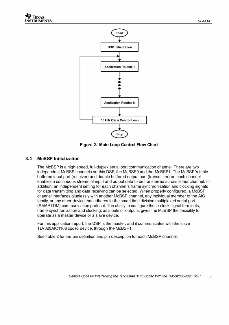
3.3 Software Loop Control
The main program for this software release has an infinite loop from within which a loop controlroutine is called continuously. It allows the loop to be repeated at a fixed frequency of 16 kHz. Itsoperation and cycling frequency are described in the subsequent paragraphs. If the user wishesto include some routines that should be repeated periodically, the routines should be placedwithin this infinite loop. These routines should be short enough to be completed within the0.0625 msec period; otherwise the 16-kHz period requirement must be relaxed.
Timer0 sets and controls an idle loop that determines the rate at which the instructions in themain loop of the main program are repeated. For this example, a cycling rate of 16 kHz is used.Assume that the DSP is configured for a 100-MHz clock rate, the required loop rate can beobtained by meeting any of the following conditions:
• Setting the Timer0 divide-down counter, MMR:TDDR to 0 and MMR:PDR to 6249, on thebasis of the LoopFrequency = 100 MHz / (MMR:TDDR + 1) / (MMR:PDR + 1) formula.
• Setting the Timer0 divide-down counter, MMR:TDDR to 4 and MMR:PDR to 1249, on thebasis of the LoopFrequency = 100 MHz / (MMR:TDDR + 1) / (MMR:PDR + 1) formula.
• Setting any combination of MMR:TDDR and MMR:PDR that would make the product of(MMR:TDDR + 1) and (MMR:PDR + 1) equal to 6250.
Upon executing the InitC5402 () routine, the Timer0 is stopped, the timer ’s MMR registers areprogrammed for the 16 kHz requirement. The Timer’s count down is subsequently kicked off,and the infinite loop of the main program is entered. After executing the body of the mainprogram, the LoopControl () routine continuously monitors the status of the Timer0’s interruptflag. Note that the timer’s interrupt does not have to be enabled since its status is being polled.Upon time-out, the interrupt flag is cleared, and control is passed back to the main loop, wherethe body of the main loop is repeated. This cycle continues indefinitely. Refer to the flow chartdepicted in Figure 2.
8/4/2019 1-246
http://slidepdf.com/reader/full/1-246 5/11
8/4/2019 1-246
http://slidepdf.com/reader/full/1-246 6/11
SLAA147
6 Sample Code for Interfaceing the TLV320AIC1106 Codec With the TMS320C5402E DSP
Table 2. McBSP Hardware Pin Description
PIN ID I/O DIRECTION DESCRIPTION
DR Input Received serial data
DX Input / Output / High – Impedance Transmitted serial data
FSR Input / Output / High – Impedance Receive frame synchronization
FSX Input / Output / High – Impedance Transmit frame synchronizat ion
CLKR Input / Output / High – Impedance Receive clock
CLKX Input / Output / High – Impedance Transmit clock
CLCKS Input External McBSP System Clock
Each McBSP channel has seven pins, through which the DSP communicates with the outsideworld. The direction and characteristics of each terminal are programmed through the McBSP’sMMR registers described in Table 3. Refer to TMS320C54x DSP Enhanced Peripherals,Reference Set Volume 5, SPRU302 [see reference 8], for more information on accessing theMcBSP control registers.
Table 3. McBSP Registers Memory Map
ADDRESS DATA MEMORY SUBADDRESS ACRONYM DESCRIPTION
McBSP0 McBSP1
0x0020 0x0040 DRR2 Data receive register 2
0x0021 0x0041 DRR1 Data receive register 1
0x0022 0x0042 DXR2 Data transmit register 2
0x0023 0x0043 DXR1 Data transmit register 1
0x0038 0x0048 SPSA Serial port subbank address register
0x0039 0x0049 SPSD Serial port subbank data register
0x0000 SPSCR1 Serial port control register 1
0x0001 SPSCR2 Serial port control register 2
0x0002 RCR1 Receive control register 1
0x0003 RCR2 Receive control register 20x0004 XCR1 Transmit control register 1
0x0005 XCR2 Transmit control register 2
0x0006 SRGR1 Sample rate generator register 1
0x0007 SRGR2 Sample rate generator register 2
0x0008 MCR1 Multichannel register 1
0x0009 MCR2 Multichannel register 2
0x000A RCERA Receive-channel enable register partition A
0x000B RCERB Receive-channel enable register partition B
0x000C XCERA Transmit-channel enable register partition A
0x000D XCERB Transmit-channel enable register partition B
0x000E PCR McBSP pin-control register
For this application report, the McBSP1 is programmed such that
• The word size is 16-bit.
• Data is left-justified.
• Frame length is 1 word per frame.
• Transmit interrupts are issued on new-frame synchs.
• The frame synch rate, i.e., sampling frequency is 8 kHz.
• CLKX or MCLK is set for 2.048 MHz.
8/4/2019 1-246
http://slidepdf.com/reader/full/1-246 7/11
SLAA147
7Sample Code for Interfaceing the TLV320AIC1106 Codec With the TMS320C5402E DSP
3.5 Interrupts
There are two types of interrupt systems on this DSP, the hardware driven interrupts which aretruly synchronous, and the software driven interrupts which are asynchronous. The C5402DSP has 30 different interrupt vectors.
• Two nonmaskable interrupts, the hardware RESET and the nonmaskable interrupt (NMI).These interrupt sources can not be disabled by software. The global interrupt enable (GIE)status has no bearing on the individual nonmaskable interrupt’s ability to interrupt anyexecution process.
• Fourteen software interrupts that can be issued at any point during the program execution. Ifcalled within a subroutine, as long as the DSP’s interrupt system is globally enabled, andthere are no interrupts of higher priority, the associated interrupt service routine (ISR) iscalled.
• Fourteen hardware peripheral interrupts that could be enabled or disable corporately byenabling or disabling the DSP’s interrupt system globally, or individually, at the designerspleasure. If all the following conditions are satisfied:
– The DSP’s interrupt system is globally enabled. – That particular interrupt is individually enabled.
– There is no other interrupt with a higher priority being serviced.
At the end of the current instruction, the CPU suspends the current routine being processed,and vectors to the associated interrupt service routine (ISR).
Upon receiving a valid interrupt request that satisfies the requirements stated above, the DSPaccesses an interrupt vector table from which it picks up the address of the corresponding ISRroutine. The application report Interfacing the TLV320AIC10/11 to the TMS320C5402 DSP ,SLAA109 [reference 1], provides a more concise description of the C5402 DSP interruptprotocol and ISR vectoring.
The McBSP1 is configured to generate a transmit interrupt (XINT) each time a framesynchronization pulse is issued. When this occurs, with no interrupts of higher priority pending,and the McBSP1’s XINT interrupt enabled, then the DSP suspends its current tasks aftercompleting the current instruction and vectors to the appropriate ISR routine, McBSP1TXISR().The ISR assumes that upon issuing a frame-sync pulse, a string of 16-bit digital data, the resultof a previous conversion, is available for reception, and that the codec is also ready to receive a16-bit string of digital data from the DSP. Within this routine, the DSP reads the result of thecodec’s left-justified analog-to-digital conversion through the McBSP1’s DRR1 register, appendsthe result with the desired receive volume gain, and sends the new data out to the codec’sdigital-to-analog converter through the McBSP1’s DXR1 register. This process simulates adigital loopback system.
The ISR used for this application example is available in the software package down load file,see the AIC1106.zip file in the product folder.
3.6 CPLD Register Initialization
The C5402 DSK has a complex programmable logic device (CPLD) through which it implementsthe various logic required for interfacing the DSP to the outside world, and at the same time,providing control and status interfaces for the DSP through software. Refer to Interfacing the TLV320AIC10/11 to the TMS320C5402 DSP , SLAA109 [see reference 1], for more details.

8/4/2019 1-246
http://slidepdf.com/reader/full/1-246 8/11
SLAA147
8 Sample Code for Interfaceing the TLV320AIC1106 Codec With the TMS320C5402E DSP
The C5402 DSK is equipped with an onboard codec unit. The onboard codec is configured to beinterfaced with the DSP through the McBSP port 0, and the onboard data access arrangement(DAA) chip is also interfaced through the McBSP port 1. However, there are only two McBSPports on this DSP. In order to accommodate a plug-in codec board, there must be a way toreroute the McBSP ports so they are alternatively connected through software to an externalunit. This is one of the functions of the CPLD. By programming various bit patterns into thecontrol register CNTL2 of the CPLD, the user chooses between routing the McBSP signals tothe various onboard peripherals, or to the plugged-in peripherals (see Figure 3). Refer to Table 4for the definition of the bits of the CLPD control register CNTL2. The appended AIC initializationassembly routine includes the set of commands required to accomplish this signal rerouting.
BSPSEL0
BSPSEL1
CPLD
McBSP0
DSP
McBSP1
Port 0
Port 1
DSP/DSKOnboard
Codec
Port 0
Port 1
Daug. Board
Plug-inCodec
Figure 3. CLDP Control Schematic
Table 4. CLDP Control Register, CNTL2
BIT POSITION ACRONYM R/W DESCRIPTION
7 DAAOH RW DAA off-hook control
6 DAACID RW DAA caller ID enable
5 FLASHENB RW External memory source selection (0 = Flash; 1 = SRAM)
4 INT1SEL RW INT1 interrupt source selection (0 = UART; 1 = daughter board)3 FC1CON RW Mic/speaker AD50 FC control
2 FC0CON RW DAA AD50 FC control
1 BSPSEL1 RW McBSP1 data source selection (0 = Mic/speaker; 1 = daughter board)
0 BSPSEL0 RW McBSP0 data source selection (0 = DAA; 1 = daughter board)

8/4/2019 1-246
http://slidepdf.com/reader/full/1-246 9/11
SLAA147
9Sample Code for Interfaceing the TLV320AIC1106 Codec With the TMS320C5402E DSP
3.7 TLV320AIC1106 Control
The AIC1106 has the capability of selecting between a linear data format and a logarithmic dataformat. If a logic 0 is applied to the LINSEL terminal of the AIC1106, the device is placed in a13-bit left-justified linear mode. If a logic 1 is applied to the LINSEL terminal of the AIC1106, thedevice is placed in a logarithmic, 8-bit left-justified µ-Law companded mode (see Table 5). In
addition, the AIC1106 codec has two mute control terminals, one for muting the microphone, andthe other for muting the earphone. Jumper settings on the TLV320AIC1106EVM required tocontrol the codec’s mute facility are given in Table 6.
Table 5. Data Conversion Format
LINSEL LOGIC STATE DATA FORMAT MODE
0 Left-justified 13-bit linear conversion
1 Left-justified 8-bit µ-Law companded conversion
Table 6. Functions and Default Settings of Jumpers W1 and W2 for the TLV320AIC1106EVM
POSITION
JUMPER DESCRIPTION 1 – 2 2 – 3 DEFAULT
W1 Microphone mute selection Mute No mute No mute
W2 Earphone mute selection Mute No mute No mute
Refer to the application report [see reference 2] on the AIC1106 hardware, for more informationon the hardware settings for this device.
In the 13-bit linear mode, the three least significant bits slot of the available 16-bit data streamthat is transmitted to the codec is used to convey the receiver volume gain code to the codecthrough the PCMI terminal. From this 16-bit string, the 13-bit digital DAC information is extractedand passed on to the DAC, and the three LSBs are passed on to the volume control circuitry,forming the receiver volume gain code (RXVOL [2:0]).
Note that if the companding option was selected, i.e., an 8-bit µ-Law format; then the ability toprogram the receiver volume gain is negated, and the default gain is fixed at 0 dB.
The desired gain is programmed into the least significant 3-bit slot of the 16-bit input PCMI datastream (see Table 7). In the companding 8-bit mode, the volume gain is fixed at 0 dB.
Table 7. Volume Control Bit Definition in Linear Mode
RXVOL [2:0] GAIN SETTING
000 3 dB
001 0 dB
010 – 3 dB
011 – 6 dB
100 – 9 dB
101 – 12 dB
110 – 15 dB
111 – 18 dB

8/4/2019 1-246
http://slidepdf.com/reader/full/1-246 10/11
SLAA147
10 Sample Code for Interfaceing the TLV320AIC1106 Codec With the TMS320C5402E DSP
3.8 Codec’s ADC/DAC Sampling Frequency
A 2.048-MHz master clock (MCLK) signal is delivered from the CLKX terminal of McBSP1 to thecodec’s MCLK terminal. In addition, the frame synchronization signal, which is also the samplingfrequency signal, assumes values up to 8 kHz. It is transmitted from the FSX terminal ofMcBSP1 to the PCMSYNC terminal of the codec. From both input signals, all the derivativeclocks required by the codec are generated internally.
3.9 Design Issues
The AIC1106 codec is easy to use because it does not have a configurable register. However,the following items must be considered:
• The LINSEL must be at the proper logic.
• The AIC1106 device has an integral PLL set at 2.048 MHz. The MCLK should be very closeto that value.
• The conversion input and output data stream are left justified and are zero-filled in eithercase, linear 13-bit or 8-bit µ-law companding. Therefore, if the user wishes to apply a gain tothe DAC codec, there is no reason to shift a previously converted data stream left by threebits before adding the 3-bit value of RXVOL [2:0]. For instance, if a – 12 dB attenuation isapplied to an A/D codec result, 101b must be added to the previous A/D result, andtransmitted to the D/A codec. This was implemented in the appended software package (seeFigure 4).
13-Bit A/D Conversion Value 3-LSB = 000b
13-Bit D/A Conversion Value RXVOL[2:0]
Figure 4. 13-Bit Linear Mode A/D and D/A Data Format
4 References
1. Interfacing the TLV320AIC10/11 to the TMS320C5402 DSP , literature number SLAA109.
2. Codec Evaluation System (SLAA141)
3. Application report TLV320AIC12/13/14/15 Codec Operating Under Stand-Alone Slave Mode literature number SLAA142
4. TMS320C54x DSP Reference Set, Volume 4: Applications Guid e, Texas Instruments Literaturenumber SPRU173
5. TLV320AIC1106 PCM CODEC data sheet, literature number SLAS357
6. TMS320C54x DSP Reference Set , Volume 1: CPU and Peripherals , Texas Instrumentsliterature number SPRU131F
7. TMS320VC5402 Fixed-Point Digital Signal Processor , data sheet, Texas Instruments literaturenumber SPRS079D
8. TMS320C54x DSP Enhanced Peripherals, Reference Set Volume 5, literature numberSPRU302
8/4/2019 1-246
http://slidepdf.com/reader/full/1-246 11/11
IMPORTANT NOTICE
Texas Instruments Incorporated and its subsidiaries (TI) reserve the right to make corrections, modifications,
enhancements, improvements, and other changes to its products and services at any time and to discontinue
any product or service without notice. Customers should obtain the latest relevant information before placing
orders and should verify that such information is current and complete. All products are sold subject to TI’s terms
and conditions of sale supplied at the time of order acknowledgment.
TI warrants performance of its hardware products to the specifications applicable at the time of sale in
accordance with TI’s standard warranty. Testing and other quality control techniques are used to the extent TI
deems necessary to support this warranty. Except where mandated by government requirements, testing of all
parameters of each product is not necessarily performed.
TI assumes no liability for applications assistance or customer product design. Customers are responsible for
their products and applications using TI components. To minimize the risks associated with customer products
and applications, customers should provide adequate design and operating safeguards.
TI does not warrant or represent that any license, either express or implied, is granted under any TI patent right,
copyright, mask work right, or other TI intellectual property right relating to any combination, machine, or process
in which TI products or services are used. Information published by TI regarding third–party products or services
does not constitute a license from TI to use such products or services or a warranty or endorsement thereof.
Use of such information may require a license from a third party under the patents or other intellectual propertyof the third party, or a license from TI under the patents or other intellectual property of TI.
Reproduction of information in TI data books or data sheets is permissible only if reproduction is without
alteration and is accompanied by all associated warranties, conditions, limitations, and notices. Reproduction
of this information with alteration is an unfair and deceptive business practice. TI is not responsible or liable for
such altered documentation.
Resale of TI products or services with statements different from or beyond the parameters stated by TI for that
product or service voids all express and any implied warranties for the associated TI product or service and
is an unfair and deceptive business practice. TI is not responsible or liable for any such statements.
Mailing Address:
Texas Instruments
Post Office Box 655303
Dallas, Texas 75265
Copyright 2002, Texas Instruments Incorporated


![Chapter 246-225 WAC RADIATION PROTECTION—X RAYS IN …leg.wa.gov/CodeReviser/WACArchive/Documents/2016/WAC 246 -225... · (6/26/08) [Ch. 246-225 WAC p. 1] Chapter 246-225 Chapter](https://img.pdfslide.net/doc/110x75/5c82589209d3f295198bd92e/chapter-246-225-wac-radiation-protectionx-rays-in-legwagovcodereviserwacarchivedocuments2016wac.jpg)


![246 ativi..[1]](https://img.pdfslide.net/doc/110x75/559fc2021a28ab0d2a8b457e/246-ativi1.jpg)


![03 AGI 246 TESIS[1]](https://img.pdfslide.net/doc/110x75/5571fac34979599169930ac5/03-agi-246-tesis1.jpg)