Embed Size (px)
Citation preview

1
4 Bit ALU
Geeping (Frank) Liu, Kasem Tantanasiriwong,
Kuo Hao Huang, Win Pratchayakun
Group 18Advisor: Dave Parent
12-1-2004

2
Abstract
• We designed a functional equivalent 74HC/HCT181 4-bit ALU that can operate at 200 MHz.
• All inputs (14) and outputs (8) of our design are connected via D flip flops.
• Total area is 390x310m2
• Power dissipation is 14.5mW, with power density of 11.9mW/cm2

3
Introduction
CMOS design has been favored by industry due to its ability to produce high-speed and high density logic circuits.
This project provides important background of CMOS design based on NMOS and PMOS characteristics. Students gain the concept of design flow as well as learning the Cadence software tools. These skills may be useful in their future careers.

4
.
4 bit ALU Features
• Full carry look-ahead for arithmetic operation• Total 16 arithmetic operations (add, subtract, plus, shift, plus 12 others)• Total 16 logic operations (XOR, AND, NAND, NOR, OR, plus 11 others)• Capable of active-high and active-low operation

5
Schematic
• Logic schematic with worst case path• Allocated different times for different logic levels. (Inverter requires much less time then a AOI)• Total time allocated to combinational logic=3.2ns• Total time allocated to each FF=.9ns

6
Design FlowProject specification
Logic function level
Transistor design level
Layout design level
Post extracted level
Functions,CLK speed, Area, Power
Final logic & timing verification Towards Schematic v.s. Layout
Timing, power verification
Timing, Sizing design for each building block
Logic verification through Verilog w/schematic
74HC/HCT181 ALU(Philips)
Design a floor plan to optimize the overall area
Layout for each block w/ DRC & LVS verification

7
Critical Path Sizing
Logic Level
Gate Cg to DriveTphl
(target)Tphl
(schematic)Tphl
(extracted)WN WP
1 Inv1 20fF 0.15ns 0.118ns 0.12ns 4.05u 7.2u
2 AOI33 321.52fF 0.9ns 0.810ns 0.732ns 8.55u 9.0u
3 AOI5432 70.2fF 0.9ns 0.518ns 0.507ns
*Decomposed AOI, uses Nand5, Nand4,
Nand3,Nand2, Inv sizing
4,5 Xor2 70.2fF 0.50ns 0.397ns 0.351ns 3.5u 5.4u
6 Nand4 39.63fF 0.6ns 0.445ns 0.407ns 4.35u 1.8u
7 Inv2 20fF 0.15ns 0.148ns 0.133ns 4.05u 7.2u
3.20ns 2.44ns 2.25ns
Methodology : 5.0 ns/(7 logic levels + 4 FF levels) =0.46 ns
*Cint=40fF
*Uses Inv1 sizing for internal inv

8
Transistor Sizing
Logic Level
GateCg to Drive
Tphl (target)
Tphl (schematic)
WN WP
Applied in AOI
Nand2 20fF 0.35ns 0.33ns 1.5u 1.5u
Nand3 50.16fF 0.35ns 0.392ns 3.75u 3.6u
Nand5 5.10fF 0.35ns 0.5ns 12.0u 4.05u
2 AOI221 186.12fF 0.9ns 0.497ns 3.15u 7.5u
3 AOI432 88.5fF 0.9ns 0.7853ns
*Decomposed AOI, uses Nand4, Nand3, Nand2, Inv
sizing
3 AOI1234 54.2fF 0.9ns 0.8367ns
*Decomposed AOI, uses Nand4, Nand3, Nand2, Inv
sizing
3 AOI32 88.5fF 0.9ns 0.55ns 5.4u 5.85u
* Non critical components were tested individually, assuming worst case scenario.

9
FF Sizing
Logic Level GateCg to Drive
Timing (target)
Timing (schematic)
Tphl (extracted)
WN WP
Master Latch
Signal TransferMux 7.89fF
0.9ns 0.67ns N/A
2.55u 4.5u
Keeper Mux 1.5u 1.5u
Nand 30.9fF 2.55u 2.1u
Slave Latch
Signal TransferMux 5fF
0.9ns .86ns
.54 ns
5.25u 9u
Keeer Mux 1.5u 1.5u
Nand 160fF 12.75u 10.95u
* Cin of DFF=12fF
10
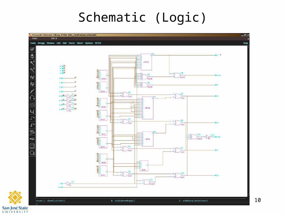
Schematic (Logic)
11
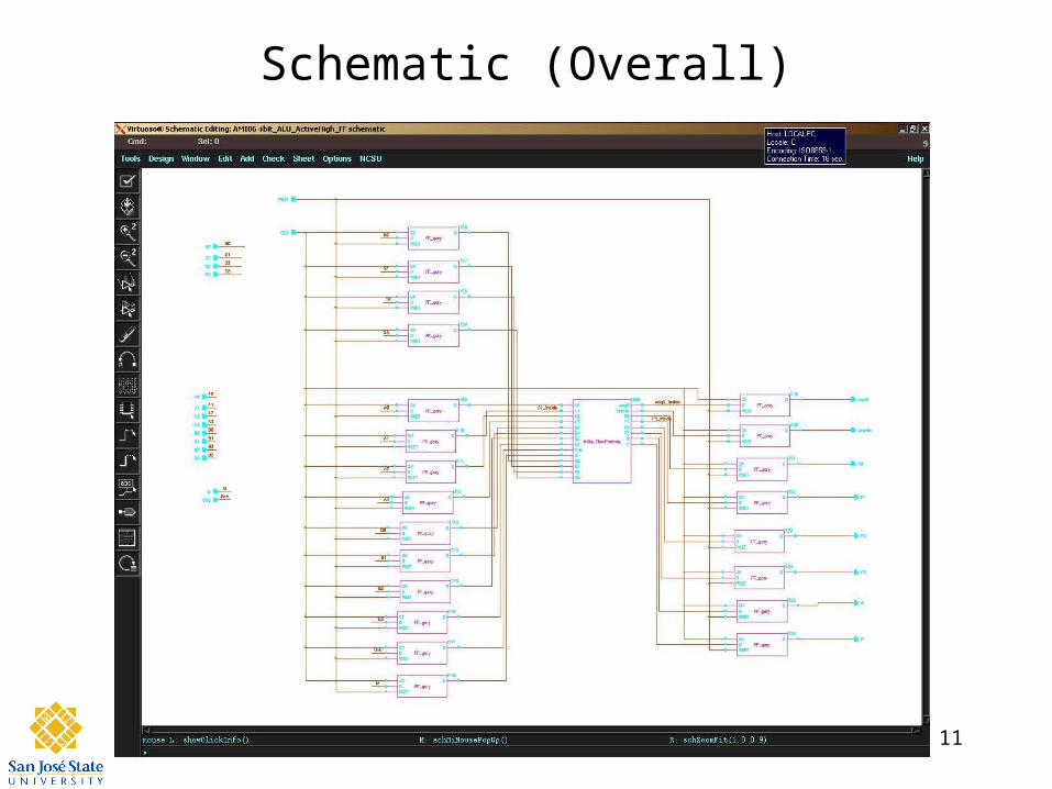
Schematic (Overall)

12
Layout (Overall)

13
Verification (Final LVS)

14
Simulations (Logic function)
A3A2A1A0 = 1010B3B2B1B0 = 1001M=1Cin=1---------------------------
S3S2S1S0 = 0000A’ = 0101
S3S2S1S0 =0110A XOR B = 0011
S3S2S1S0 =1011A AND B = 1000
S3S2S1S0 =1110A OR B = 1011

15
Simulations (Arithmetic function)
A3A2A1A0 = 1010B3B2B1B0 = 1001M=0Cin=1--------------------------------
S3S2S1S0 = 0110A minus B minus 1= 0000
S3S2S1S0 =1001A plus B = 0011
S3S2S1S0 =1100A plus A (shift left) = 0100
S3S2S1S0 =1111A minus 1 = 1001

16
Power
Power = 58 mW / 4 clocks = 14.5mw
17
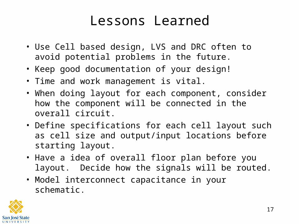
Lessons Learned
• Use Cell based design, LVS and DRC often to avoid potential problems in the future.
• Keep good documentation of your design!
• Time and work management is vital.
• When doing layout for each component, consider how the component will be connected in the overall circuit.
• Define specifications for each cell layout such as cell size and output/input locations before starting layout.
• Have a idea of overall floor plan before you layout. Decide how the signals will be routed.
• Model interconnect capacitance in your schematic.

18
Summary
• Our design met all the specifications, speed 200Mhz, area 390um*310um, power dissipation 14.5 mW, Power density 11.9 W/cm2
• This project provided some insight of the various aspects of the design process. By doing the design, we understand many of the problems design engineers face.
• As feature size decreases, factors such as interconnect and parasitic capacitance will have a bigger impact on design
19
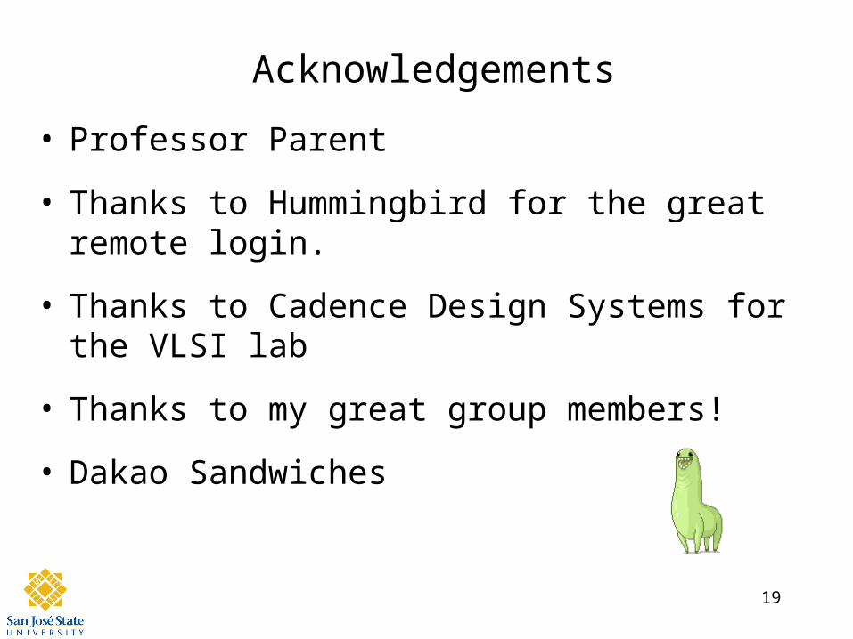
Acknowledgements
• Professor Parent
• Thanks to Hummingbird for the great remote login.
• Thanks to Cadence Design Systems for the VLSI lab
• Thanks to my great group members!
• Dakao Sandwiches

20
Misc