Embed Size (px)
Citation preview

1
Chapter 3
Logic Gates

2
Inverter

3
Inverter Truth Table

4
Inverter Timing Diagram
Figure 3--2 Inverter operation with a pulse input.
Figure 3--6 The inverter complements an input variable.

5
Inverter Timing Diagram

6
AND gate

7
Figure 3--9 All possible logic levels for a 2-input AND gate.
AND Gate Operation

8
AND Gate Truth Table
Figure 3--14 Boolean expressions for AND gates with two, three, and four inputs.

9
AND Gate Truth Table

10
AND Gate Timing Diagram
Figure 3--10 Example of pulsed AND gate operation with a timing diagram showing input and output relationships.

11
AND Gate Timing Diagram
All must be high for the output to be high

12
Figure 3--15 An AND gate performing an enable/inhibit function for a frequency counter.
AND Gate Application Example

13
OR Gate

14
Figure 3--18 All possible logic levels for a 2-input OR gate
OR Gate Operation
15
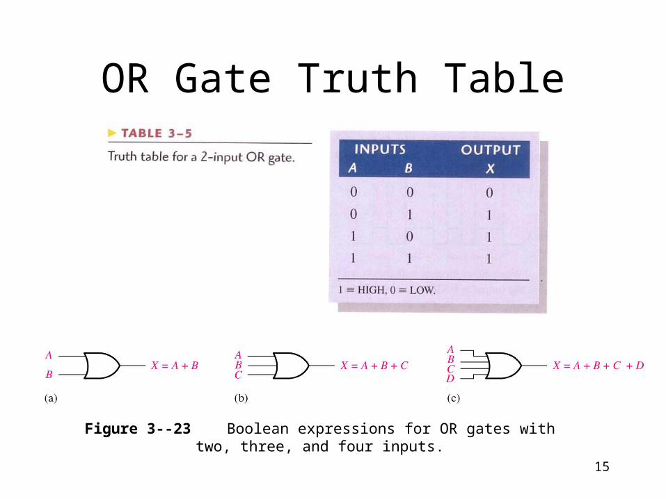
OR Gate Truth Table
Figure 3--23 Boolean expressions for OR gates with two, three, and four inputs.

16
OR Gate Timing Diagram
Figure 3--19 Example of pulsed OR gate operation with a timing diagram showing input and output time relationships.

17
OR Gate Timing Diagram
All must be low for the output to be low

18
OR Gate Application Example
Figure 3--24 A simplified intrusion detection system using an OR gate.

19
NAND Gate

20
Figure 3--26 Operation of a 2-input NAND gate.
NAND Gate Operation

21
NAND Gate Truth Table

22
NAND Gate Timing Diagram
ABX

23
Figure 3--29 Standard symbols representing the two equivalent operations of a NAND gate.

24
NOR Gate

25
NOR Gate Operation
Figure 3--34 Operation of a 2-input NOR gate.

26
NOR Gate Truth Table

27
NOR Gate Timing Diagram
BAX

28
Figure 3--37 Standard symbols representing the two equivalent operations of a NOR gate.

29
XOR Gate

30
XOR Gate Operation
Figure 3--42 All possible logic levels for an exclusive-OR gate

31
XOR Gate Truth Table
BAX

32
XOR Gate Application Example
Figure 3--48 An XOR gate used to add two bits.

33
XNOR Gate

34
XNOR Gate Operation
Figure 3--45 All possible logic levels for an exclusive-NOR gate.

35
XNOR Gate Truth Table
BAX

36
Fixed-Function Logic : IC Gates
• CMOS (Complementary Metal-Oxide Semiconductor)
• TTL (Transistor-Transistor Logic)
• CMOS – lower power dissipation

37
Figure 3--49 Typical dual in-line (DIP) and small-outline (SOIC) packages showing pin numbers and basic dimensions.

38
Figure 3--50 Pin configuration diagrams for some common fixed-function IC gate configurations.
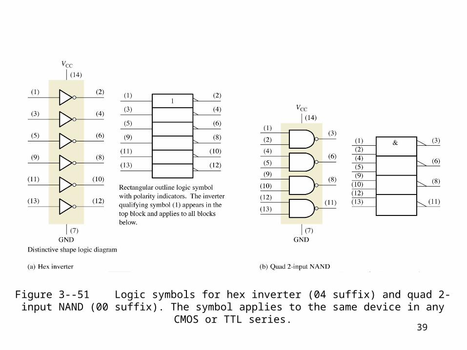
39
Figure 3--51 Logic symbols for hex inverter (04 suffix) and quad 2-input NAND (00 suffix). The symbol applies to the same device in any CMOS or TTL series.

40
Performance Characteristics and Parameters
• Propagation delay Time
• DC Supply Voltage (VCC)
• Power Dissipation
• Input and Output Logic Levels
• Speed-Power product
• Fan-Out and Loading

41
Figure 3--52 Propagation Delay

42Figure 3--53 The LS TTL NAND gate output fans out to a maximum of 20 LS TTL gate inputs.
Higher fan-out = gate can be connected to more gate inputs.

43Figure 3--57 The partial data sheet for a 74LS00.

44
Figure 3--59 The effect of an open input on a NAND gate.
Troubleshooting

45
Figure 3--60 Troubleshooting a NAND gate for an open input with a logic pulser and probe.

46
Programmable Logic• Programmable Arrays
Figure 3--65 An example of a basic programmable OR array.
47
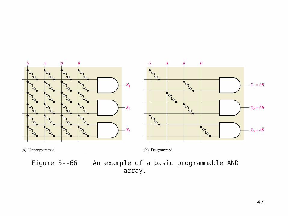
Figure 3--66 An example of a basic programmable AND array.

48
Figure 3--67 Block diagram of a PROM (programmable read-only memory).
4 Types of SPLDs

49
Figure 3--68 Block diagram of a PLA (programmable logic array).

50
Figure 3--69 Block diagram of a PAL (programmable array logic).

51
Figure 3--70 Block diagram of a GAL (generic array logic).

52
Figure 3--71 Logic Gate Summary