Embed Size (px)
Citation preview
3
1. Divergence of the three dimensional radial vector field is
A. 3
B.
C.
D.
2. If ),,( zyx is a scalar function, then
is
A. 1
B. 0
C. 3
D. -3
3. If )(sF is the Laplace transform of )(tf , then the Laplace transform of t
df0
)( is
equal to
A. )(1
sFs
s
B. )(1
sFs
C. )(ssF
D. dssF )(
4. Given a matrix
34
24, one of its eigen vectors is
A.
2
1
B.
2
3
C.
1
2
D.
3
4

4
5. If x and y satisfy the implicit function 0),( xy yxyxf , then x
y
d
dis given by
A.
xy
x
yx
y
ln
ln
B.
xx
y
yy
x
ln
ln
C. 2
2
x
y
y
x
D. xyx
yxy
ln
ln
6. The Newton Raphson method formula for finding the square root of a real number R
from the equation 02 Rx is
A. 2
1i
i
xx
B. 2
31
ii
xx
C.
iii
x
Rxx 3
2
11
D.
iii
x
Rxx
2
11
7. Determinant of a 5 × 5 orthogonal matrix can take values
A. 0
B. 1 C. 25
D. 5
8. The signal )(tx is described by otherwise 0 and ,11for 1)( x(t)ttx . The two
angular frequencies at which its Fourier transform becomes zero are
A. 5.0 , 5.1
B. 0 ,
C. , 2
D. 5.0 , 5.2
5
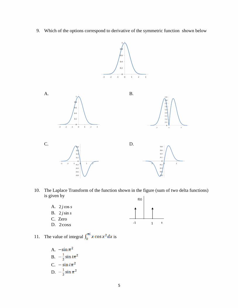
9. Which of the options correspond to derivative of the symmetric function shown below
A.
B.
C.
D.
10. The Laplace Transform of the function shown in the figure (sum of two delta functions)
is given by
A. sj cos2
B. sj sin2
C. Zero
D. scos2
11. The value of integral is
A.
B.
C.
D.
t -1
f(t)
1
6
12. If Laplace transform of is then Laplace transform of
is
A.
B.
C.
D.
13. If f(x) is a symmetric periodic function of x, then the Fourier series of the function f(x)
will be of the form
A.
B.
C.
D.
14. If ˆˆ ˆr xi yj zk
, then 2
( )rgrad e has the value
A. 2
2 rrre
B. 2
2 rre
C. 21
2
rre
D. 2rre
15. The complete solution of the differential equation 2
25 6 xd y dy
y edx dx
is:
A. 2
1 22
xx x e
y c e c e
B. 2 3
1 22
xx x e
y c e c e
C. 22
1 3
2
2
1
xxx e
ececy
D. 2
1 2( )2
xx e
y c c x e
7
16. The value of the contour integral
C z
z2
2
3, C is the unit circle (counterclockwise) is
A. 24πi
B. 0
C. 12πi
D. 6πi
17. The Laplace transform of t
tf3
)(
is
A. 3s
B. 33
C. 3
D. 3 s
18. The intensity pattern shown in the figure is the diffraction pattern for a N-slit array with
slit width b and slit seperation a . The values of N and b
aare
A. 2 and 3
B. 3 and 2
C. 4 and 3
D. 5 and 2
19. In the design of a single mode step index optical fiber close to upper cut off , the single
mode operation is NOT preserved if
A. radius as well as operating wavelength are halved
B. radius as well as operating wavelength are doubled
C. radius is doubled and operating wavelength is halved
D. radius is halved and operating wavelength is doubled
20. The work function of silver and sodium are 4.6 eV and 2.3 eV respectively. The ratio of
the slope of the stopping potential versus frequency plot for silver and sodium in a
photoelectric effect experiment is
A. 2
1
B. 2
C. 1
D. 2
8
21. The refractive index of glass is 1.5. The wavelength of light with frequency 1014
Hz in
glass is
A. m 2
B. m 3
C. m .54
D. m 1
22. The wave function of a quantum mechanical particle is given by
)(5
4)(
5
3)( 21 xxx
where )(1 x and )(2 x are eigenfunctions with eigenvalues -1 eV and -2 eV respectively.
The energy of the particle in the state )(x is
A. 5
11
B. 25
41
C. 25
36
D. 5
7
23. Unpolarized light of intensity I0 is incident on two ideal linear polarizers whose
transmission axes differ by 60 degrees. The intensity of the transmitted light is
A. 4
I0
B. 2
I0
C. 8
I0
D. 4
3I0
24. X rays are
A. Cathode rays and are made of electrons
B. Positive rays and made of positrons.
C. Neutral and made of photons.
D. Neutral and made of neutrons.

9
25. If λo is the de Broglie wavelength for a proton accelerated through a potential V, then the
de Broglie wavelength for an α particle accelerated through the same potential is
A. 22/o
B. o22
C. 2/o
D. 2/o
26. In C language, which of the following special symbols is allowed in a variable name?
A. * (asterisk)
B. _ (underscore)
C. | (pipeline)
D. – (hyphen)
27. In the C program given below, point out the error, if any, in the for loop
main()
int i=1;
for (;;)
printf(“%d”, i++);
if(i>10)
break;
A. The condition in the for loop is a must.
B. The two semicolons should be dropped.
C. The for loop should be replaced by a while loop.
D. No error.
28. In C language, which function is used to round off a value from 1.66 to 2.0?
A. floor(1.66)
B. roundup(1.66)
C. ceil(1.66)
D. rountdto(1.66)

10
29. What would be the output of the following C program, if the array begins at address
1200?
main()
int arr[ ] = 2,3,4,1,6;
printf(“%d%d”, arr, sizeof(arr));
A. 1201 5
B. 1200 1024
C. 1201 1024
D. 1200 10
30. If the sequence of operation – push (1), push (2), pop, push (1), push (2), pop, pop,
pop, push (2), pop are performed on a stack, the sequence of the popped out values are
A. 2 2 1 2 2
B. 2 1 1 2 2
C. 2 2 1 1 2
D. 2 1 2 2 2
31. Which of the following is a PNPN device and has two common gates ?
A. DIAC
B. SCR
C. BJT
D. TRIAC
32. A n-type semiconductor has Hall coefficient of 150 cm3/C and resistivity ρ = 0.05 Ω cm.
The electron mobility will be
A. 3000 cm2/V-s
B. 2560 cm2/V-s
C. 25.60 cm2/V-s
D. 2000 cm2/V-s
33. When temperature is increased from room temperature the resistivity of an intrinsic
semiconductor
A. decreases
B. increases
C. becomes zero
D. does not change
11
34. The diamond crystal structure is formed by
A. two interlaced bcc unit cells
B. three interlaced fcc unit cells
C. three interlaced bcc unit cells
D. two interlaced fcc unit cells
35. The longest wavelength that can be used to analyze the NaCl crystal planes of spacing
d = 2.82 Å in the first order is
A. 1.45 × 10⁻¹⁰
m
B. 2.82 × 10⁻¹⁰
m
C. 5.64 × 10⁻¹⁰
m
D. 4.64 × 10⁻¹⁰
m
36. If the Fermi energy is 3kT above the edge of the conduction band, then the probability of
finding an electron at the Fermi energy EF is
A. 1.0
B. 0.3
C. 0.7
D. 0.5
37. The density of impurity atoms that must be added to intrinsic silicon to convert it to
10-1
Ω m p-type silicon with hole mobility 0.05 m2/V is
A. 1.25 × 10¹⁷
/m3
B. 1.25 × 10²¹
/m3
C. 1.25 × 10²¹
/cm3
D. 1.25 × 10¹⁷
/cm3
38. In case of intrinsic semiconductors the Fermi level EF lies exactly in the center of the
forbidden energy gap Eg when
A. the effective mass of a hole is equal to the effective mass of the free electron
B. the effective mass of a hole is less than the effective mass of the free electron
C. the effective mass of a hole is greater than the effective mass of the free electron
D. the charge of a hole is equal to charge of an electron
39. In a typical Hall effect experiment, if a 1.6 mm thick sample of n-type germanium
with donor density 1021
/m3 is placed in a magnetic field of 5 weber/m
2, the Hall voltage
developed for a current density of 500 A/m2 is
A. 40 mV
B. 35 mV
C. 10 mV
D. 25 mV

12
40. When a p-n junction diode is forward biased
A. the depletion region is reduced and barrier height is increased
B. both the depletion region and barrier height are reduced
C. the depletion region is increased and barrier height is reduced
D. both the depletion region and barrier height are increased
41. In a p-n junction, the depletion layer consists of
A. immobile ions
B. protons
C. electrons
D. mobile ions
42. An ideal diode should have
A. zero resistance in forward bias as well as reverse bias
B. zero resistance in forward bias and an infinitely large resistance in reverse bias
C. infinitely large resistance in reverse bias
D. infinitely large resistance in forward as well as reverse bias
43. The minimum gate current which can turn an SCR on is called
A. holding current
B. trigger current
C. junction current
D. break over current
44. A UnijunctionTransistor (UJT) has
A. one emitter and two bases
B. two emitters and one base
C. one emitter and one base
D. two emitters and two bases
45. What are the bias conditions of the emitter-base and collector-base junctions
respectively for a BJT to operate as an amplifier?
A. Reverse; Forward
B. Reverse; Reverse
C. Forward; Reverse
D. Forward; Forward

13
46. To make a good non-rectifying contact between a metal and n-type semiconductor,
A. the semiconductor should be lightly doped
B. the work function of metal should be greater than the work function of
semiconductor
C. the work function of metal should be lower than the work function of
semiconductor
D. the metal should have a high Schottky barrier height
47. For an ideal JFET, when VDS is increased beyond the pinch off point, the drain current
A. remains constant
B. increases
C. decreases
D. first decreases and then increases
48. If the forward current–voltage characteristic of a p-n junction diode has a slope of 50
mA/V at a desired point then the approximate incremental resistance of the diode is
A. 20 Ω
B. 50 Ω
C. 10 Ω
D. 35 Ω
49. In an n-channel enhancement MOSFET, at a fixed drain voltage
A. the drain current has a finite value at zero gate voltage and it increases with
applied negative gate voltage.
B. the drain current is zero at zero gate voltage and it increases with the applied
positive gate voltage.
C. the drain current is maximum at zero gate voltage and it decreases with applied
negative gate voltage.
D. the drain current is maximum at zero gate voltage and it decreases with positive
gate voltage.
50. If a transistor has 97.0 then the value of β is
A. 32.33
B. 0
C. 1
D. 2.94
14
32V
6A 24Ω
8Ω I2 RL 14Ω
51. Consider the following statements associated with reciprocal two port networks:
1. Z12 = Z21 2. Y12 = Y21 3. h12 = h21 4. AD-BC =1
Which of the statements given above are correct ?
A. 1,2,3
B. 1,2,4
C. 1,3,4
D. 2,3,4
52. In an RLC circuit )6
5314sin(20)(
ttv and )
3
2314sin(10)(
tti . The power
factor of the circuit is
A. 0.5
B. 0.707
C. 1.0
D. 0.866
53. The value of R in the circuit when the current is zero in the branch AB is
A. 60 Ω
B. 20 Ω
C. 40 Ω
D. 30 Ω
54. If each branch of a delta circuit has an impedance Z3 , then each branch of the
equivalent Y circuit has an impedance
A. 3
Z
B. 3Z
C. 3 3Z
D. 3
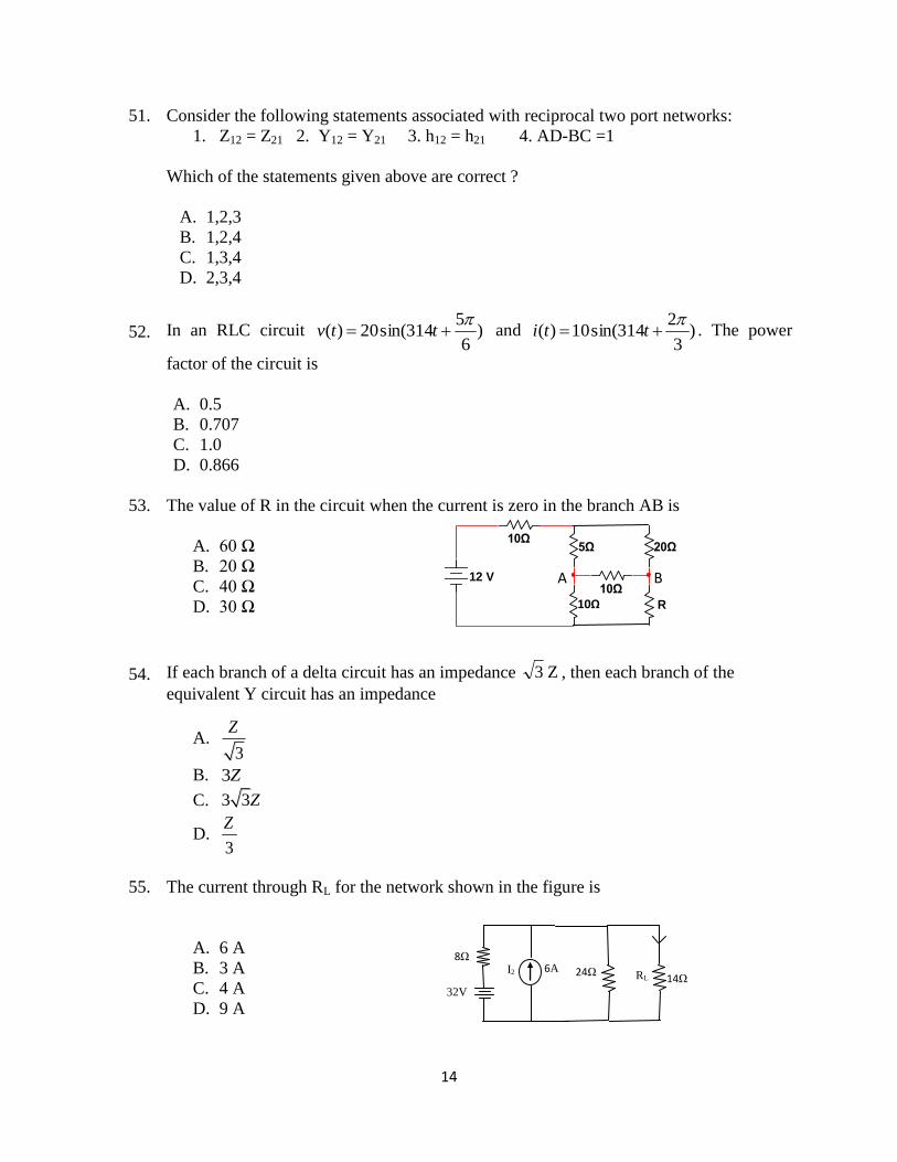
Z
55. The current through RL for the network shown in the figure is
A. 6 A
B. 3 A
C. 4 A
D. 9 A
12 V
10Ω5Ω
5Ω
10Ω
20Ω
R
A B
10Ω
15
56. The inductance of a coil in which the current increases linearly from 0 to 0.2 A in a time
interval of 0.3 sec producing a voltage of 10 V is
A. 9 H
B. 10 H
C. 15 H
D. 1.5 H
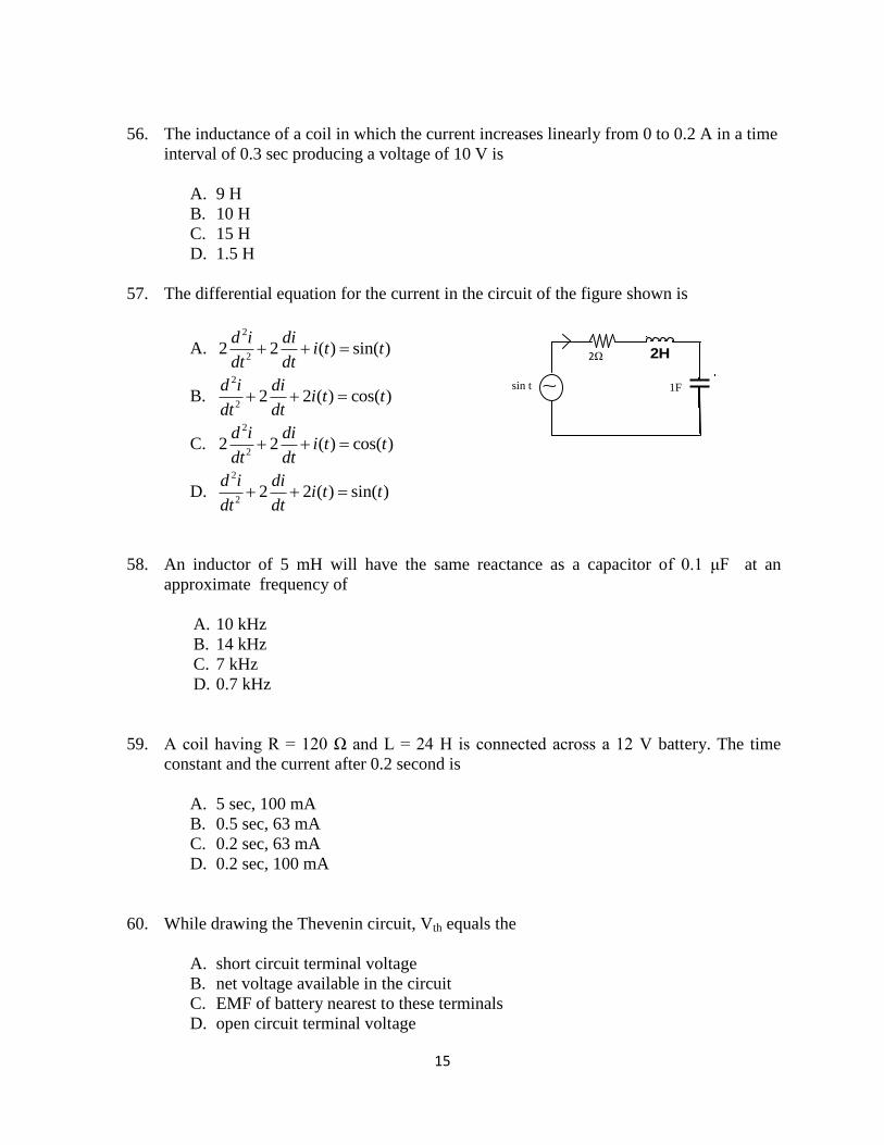
57. The differential equation for the current in the circuit of the figure shown is
A. 2
22 2 ( ) sin( )
d i dii t t
dt dt
B. 2
22 2 ( ) cos( )
d i dii t t
dt dt
C. 2
22 2 ( ) cos( )
d i dii t t
dt dt
D. 2
22 2 ( ) sin( )
d i dii t t
dt dt
58. An inductor of 5 mH will have the same reactance as a capacitor of 0.1 μF at an
approximate frequency of
A. 10 kHz
B. 14 kHz
C. 7 kHz
D. 0.7 kHz
59. A coil having R = 120 Ω and L = 24 H is connected across a 12 V battery. The time
constant and the current after 0.2 second is
A. 5 sec, 100 mA
B. 0.5 sec, 63 mA
C. 0.2 sec, 63 mA
D. 0.2 sec, 100 mA
60. While drawing the Thevenin circuit, Vth equals the
A. short circuit terminal voltage
B. net voltage available in the circuit
C. EMF of battery nearest to these terminals
D. open circuit terminal voltage
sin t
2Ω
1F
2H
16
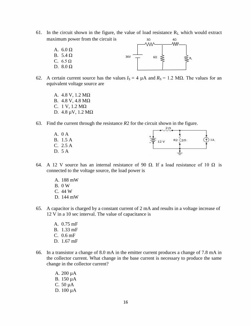
61. In the circuit shown in the figure, the value of load resistance RL which would extract
maximum power from the circuit is
A. 6.0 Ω
B. 5.4 Ω
C. 6.5 Ω D. 8.0 Ω
62. A certain current source has the values IS = 4 µA and RS = 1.2 MΩ. The values for an
equivalent voltage source are
A. 4.8 V, 1.2 MΩ
B. 4.8 V, 4.8 MΩ
C. 1 V, 1.2 MΩ
D. 4.8 µV, 1.2 MΩ
63. Find the current through the resistance R2 for the circuit shown in the figure.
A. 0 A
B. 1.5 A
C. 2.5 A
D. 5 A
64. A 12 V source has an internal resistance of 90 Ω. If a load resistance of 10 Ω is
connected to the voltage source, the load power is
A. 188 mW
B. 0 W
C. 44 W
D. 144 mW
65. A capacitor is charged by a constant current of 2 mA and results in a voltage increase of
12 V in a 10 sec interval. The value of capacitance is
A. 0.75 mF
B. 1.33 mF
C. 0.6 mF
D. 1.67 mF
66. In a transistor a change of 8.0 mA in the emitter current produces a change of 7.8 mA in
the collector current. What change in the base current is necessary to produce the same
change in the collector current?
A. 200 µA
B. 150 µA
C. 50 µA
D. 100 µA
RL
3Ω
36V 6Ω
4Ω
17
67. Resonance frequency of a parallel LC resonance circuit is
A. LC
1Hz
B. LC2
1Hz
C. LC Hz
D. LC
2Hz
68. A chopper has a supply voltage of 200 V dc, ON time of 30 ms and OFF time of 10 ms.
The duty cycle and average dc output voltage are
A. 0.50 and 100V
B. 0.50 and 150V
C. 0.75 and 150V
D. 0.75 and 100V
69. A negative feedback amplifier has an internal gain A=100 and feedback factor =0.1. Its
gain with feedback will be
A. 0.11
B. 9.09
C. 11.1
D. 109.9
70. An ideal current source is one whose internal resistance is
A. zero
B. very high
C. very low
D. Infinite
71. The figure shown below represents an op amp circuit. If R1 = infinity and R2 = 0, then
the circuit is
A. an inverting amplifier with ideal gain infinity
B. an inverting amplifier with Vo = 0
C. a non inverting amplifier with Vo = Vin
D. a non inverting amplifier with ideal gain infinity
18
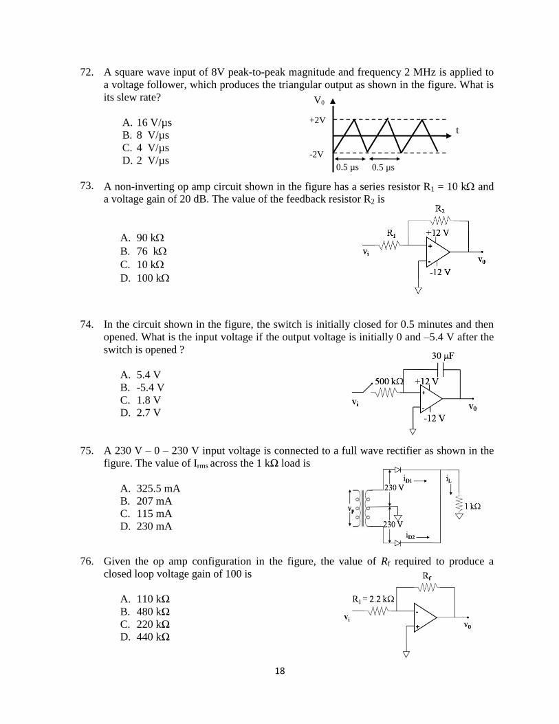
72. A square wave input of 8V peak-to-peak magnitude and frequency 2 MHz is applied to
a voltage follower, which produces the triangular output as shown in the figure. What is
its slew rate?
A. 16 V/µs
B. 8 V/µs
C. 4 V/µs
D. 2 V/µs
73. A non-inverting op amp circuit shown in the figure has a series resistor R1 = 10 k and
a voltage gain of 20 dB. The value of the feedback resistor R2 is
A. 90 k
B. 76 k
C. 10 k
D. 100 k
74. In the circuit shown in the figure, the switch is initially closed for 0.5 minutes and then
opened. What is the input voltage if the output voltage is initially 0 and –5.4 V after the
switch is opened ?
A. 5.4 V
B. -5.4 V
C. 1.8 V
D. 2.7 V
75. A 230 V – 0 – 230 V input voltage is connected to a full wave rectifier as shown in the
figure. The value of Irms across the 1 kΩ load is
A. 325.5 mA
B. 207 mA
C. 115 mA
D. 230 mA
76. Given the op amp configuration in the figure, the value of Rf required to produce a
closed loop voltage gain of 100 is
A. 110 kΩ
B. 480 kΩ
C. 220 kΩ
D. 440 kΩ
V0
+2V
-2V
t
0.5 µs 0.5 µs
19
77. The maximum peak output voltage obtainable from a741 op-amp circuit with a 100 KHz
frequency (SR = 0.5V / µs) is
A. 0.79 V
B. 0.25 V
C. 0.95 V
D. 0.40 V
78. For a JFET with IDSS = 15mA and Vgs(off) = -5 V, the drain current for Vgs = -2V is
A. 58.8 mA
B. 29.4 mA
C. 9.6 mA
D. 5.4 mA
79. If (11X1Y)8 = (12C9)16, then the values of X and Y are
A. 3 and 1
B. 5 and 7
C. 7 and 5
D. 1 and 5
80. In an 8085 microprocessor, the numbers are represented in signed 2's complement form
as P = 11101101 and Q = 11100110. If Q is subtracted from P, the value obtained in
signed 2's complement form is
A. 100000111
B. 00000111
C. 11111001
D. 011111001
81. An analog voltage of 3.4 V is converted into a 8-bit digital form by an A/D converter
with the reference voltage of 5 V. The digital output is
A. 11110001
B. 10101110
C. 10011001
D. 10110111
82. A bistable multi-vibrator that functions as a voltage comparator with hysteresis is called
A. D Flip Flop
B. Schmitt Trigger
C. T Flip Flop
D. J-K Flip Flop
20
83. The Figure of Merit of a logic family is given by
A. Gain Bandwidth Product
B. (Propagation Delay Time) x (Power Dissipation)
C. (Fan Out) x (Propagation Delay time)
D. (Noise Margin) x (Power Dissipation)
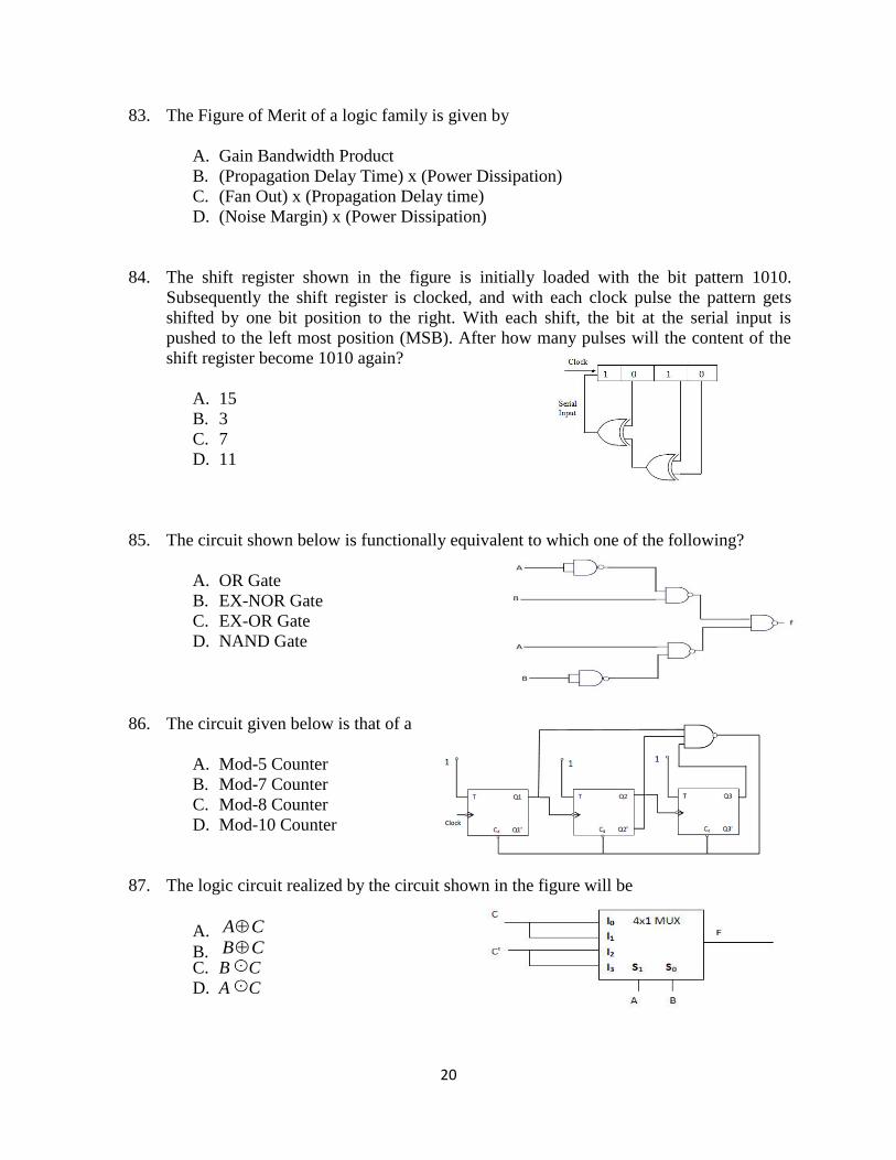
84. The shift register shown in the figure is initially loaded with the bit pattern 1010.
Subsequently the shift register is clocked, and with each clock pulse the pattern gets
shifted by one bit position to the right. With each shift, the bit at the serial input is
pushed to the left most position (MSB). After how many pulses will the content of the
shift register become 1010 again?
A. 15
B. 3
C. 7
D. 11
85. The circuit shown below is functionally equivalent to which one of the following?
A. OR Gate
B. EX-NOR Gate
C. EX-OR Gate
D. NAND Gate
86. The circuit given below is that of a
A. Mod-5 Counter
B. Mod-7 Counter
C. Mod-8 Counter
D. Mod-10 Counter
87. The logic circuit realized by the circuit shown in the figure will be
A. A C
B. B C C. B C
D. A C

21
88. The octal form of the decimal number is
A. 231.42
B. 231.41
C. 231.40
D. None of the above
89. 10’s Compliment of the number 012398 is
A. 987601
B. 087602
C. 987602
D. 087601
90. The simplified form of the Boolean function ))(( BABA is
A. B
B. 1
C.
D. A
91. A logic circuit that gives a HIGH output for both inputs HIGH or both inputs LOW is
A. an Ex-NOR gate
B. an OR gate
C. an Ex-OR gate
D. a NAND date
92. For the Karnaugh map given below, the simplified Boolean function is
A.
B.
C.
D.
93. The 8-input XOR circuit shown has an output of Y = 1. Which input combination below
(ordered A – H) is correct?
A. 10111000
B. 11100111
C. 10111100
D. 00011101

22
94. Which of the following flags in 8086 microprocessor get affected by the instruction
CMP ?
A. Trap Flag
B. Carry Flag
C. Parity Flag
D. Sign Flag
95. Consider the following instructions executed in the 8086 microprocessor
PUSH AX; AX 40 H in it
PUSH BX; BX 18 H in it
POP AX;
POP G
The value stored in G will be
A. 28 H
B. 12 H
C. 40 H
D. 68 H
96. Which of the following instructions of an 8086 microprocessor uses the content of a CX
register as a counter?
A. LOOP
B. LOCK
C. LDA
D. CALL
97. In a 8086 microprocessor, if the content of the code segment register is 1FAB and the
content of the IP register is 10A1, then the effective memory address is
A. 1FBC0
B. 30AC
C. FDB5
D. 20B51
98. Which one of the following interrupts is both level and edge sensitive?
A. RST 7.5
B. RST 6.5
C. TRAP
D. INTR
23
99. Which one of the following modes is required for 8253 to generate a square wave?
A. MODE 1
B. MODE 3
C. MODE 2
D. MODE 4
100. The interface chip used for data transmission between 8086 and a 16-bit ADC is
A. 8251
B. 8253
C. 8255
D. 8259
101. The 8086 and 8253 run at 6 MHz and 1.5 MHz respectively. The number of T-states
required to generate a square wave of period 1 ms is
A. 1500 states
B. 3000 states
C. 6000 states
D. 1000 states
102. After the following instruction is executed in a 8086 microprocessor
LOAD X
MULT Y
STORE T1
LOAD Z
ADD Y
ADD T1
STORE R
A. R = X+XY+Z
B. R = X+Y+XZ
C. R = XY+Y+Z
D. R = XY+Y+XZ
103. To have multiprocessing capabilities of the 8086 microprocessor, the pin connect to the
ground is
A. MXMN / with logic 1
B. ALE
C. INTR
D. MXMN / with logic 0

24
104. By which of the following ways can a microprocessor come out of the HALT state?
A. When HOLD line is logical 1
B. When the interrupt occurs and the interrupt system has been enabled
C. When both A and B are true
D. When either A or B are true
105. In the instruction FADD, F stands for
A. Far
B. Floppy
C. File
D. Floating
106. What will be the contents of register AL after the following has been executed ?
MOV BL,8C
MOV AL, 7E
ADD AL,BL
A. 0A and carry flag is reset
B. 0A and carry flag is set
C. 6A and carry flag is set
D. 6A and carry flag is reset
107. READY pin of a microprocessor is used
A. to introduce wait states
B. to indicate microprocessor is ready to receive inputs
C. to indicate microprocessor is ready to receive outputs
D. to provide direct memory access
108. Pseudo instructions are basically
A. false instructions
B. instructions that are ignored by the microprocessor.
C. instructions that are treated like comments
D. assembler directives
109. A rectangular waveguide of internal dimensions cm 4a , cm 3b is to be operated in
the TE11 mode. The minimum operating frequency is
A. 6.0 GHz
B. 3.75 GHz
C. 5.0 GHz
D. 6.25 GHz
25
110. For a Hertz dipole antenna, the half power beam width in the E-Plane is
A. 360ο
B. 180ο
C. 45ο
D. 90ο
111. The electric field of a time harmonic plane EM wave travelling in a non-magnetic,
lossless dielectric medium has an amplitude of 1 V/m. If the relative dielectric constant
of the medium is 4, the magnitude of the time averaged Poynting vector is
A. 240
1
B. 60
1
C. 30
1
D. 120
1
112. A transmission line has a characteristic impedance of 50Ω and resistance of 1.0 Ω/m. If
the line is distortionless, the attenuation constant (in Np/m) is
A. 0.002
B. 5.0
C. 500
D. 0.014
113. The power radiated by a Hertzian dipole antenna fed by a peak current 0I is given
by
2200
3
dlIP . The radiation resistance of the antenna is approximately
A. 2
2790
dl
B.
dl280
C. 2
280
dl
D. 2
80
dl
26
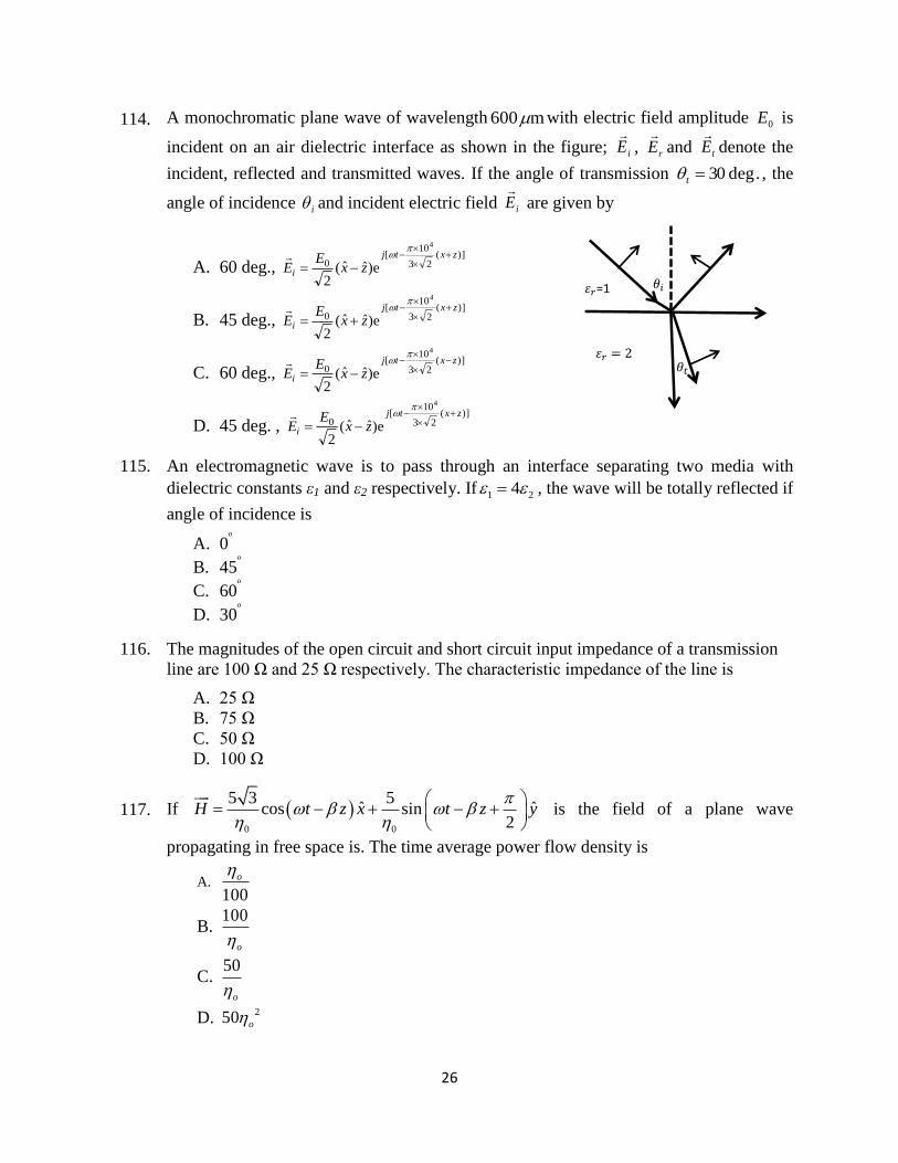
=1
114. A monochromatic plane wave of wavelength m 600 with electric field amplitude 0E is
incident on an air dielectric interface as shown in the figure; iE
, rE
and tE
denote the
incident, reflected and transmitted waves. If the angle of transmission .deg30t , the
angle of incidence i and incident electric field iE
are given by
A. 60 deg., )](
23
10[
0
4
e)ˆˆ(2
zxtj
i zxE
E
B. 45 deg., )](
23
10[
0
4
e)ˆˆ(2
zxtj
i zxE
E
C. 60 deg., )](
23
10[
0
4
e)ˆˆ(2
zxtj
i zxE
E
D. 45 deg. , )](
23
10[
0
4
e)ˆˆ(2
zxtj
i zxE
E
115. An electromagnetic wave is to pass through an interface separating two media with
dielectric constants ε1 and ε2 respectively. If 1 24 , the wave will be totally reflected if
angle of incidence is
A. 0ᵒ
B. 45ᵒ
C. 60ᵒ
D. 30ᵒ
116. The magnitudes of the open circuit and short circuit input impedance of a transmission
line are 100 Ω and 25 Ω respectively. The characteristic impedance of the line is
A. 25 Ω
B. 75 Ω
C. 50 Ω
D. 100 Ω
117. If 0 0
5 3 5ˆ ˆcos sin
2H t z x t z y
is the field of a plane wave
propagating in free space is. The time average power flow density is
A. 100
o
B. 100
o
C. 50
o
D. 250 o

27
118. The amplitude of the magnetic field of a plane wave propagating in a medium
characterized by =0, =0 and =40 is 2A/m. The magnitude of the electric field will
be
A. 80 V/m
B. 120 V/m
C. 60 V/m
D. 20 V/m
119. For a plane wave propagating in a lossless medium, the wavelength is 0.25 m and the
frequency is 600 MHz. The permittivity of the medium will be
A. 6
B. 3
C. 2
D. 4
120. When a EM wave propagates in a lossy dielectric medium, as the conductivity increases
the phase constant
A. decreases
B. remains unchanged
C. zero
D. increases
121. The medium 1 and 2 have relative permittivities 1 and 2, respectively, then Brewster's
angle B for a wave travelling from medium 2 to medium 1 is
A. 2
1tan
B
B. 1
2tan
B
C. 21tan B
D. 212tan B
122. If the Coulomb force acting on a charge of 10 C is yx aaF ˆ4ˆ3
N, the magnitude of
the electric field is
A. 0.5 V/m
B. 10 V/m
C. 7 V/m
D. 1.2 V/m
28
123. A coaxial cable with characteristic impedance 50 is insulated with a dielectric, whose
relative permittivity is 1.0. The phase velocity of the waves on this coaxial cable at 10
GHz will be
A. 2.71010
cm/s
B. 3.61010
cm/s
C. 31010
cm/s
D. 1.91010
cm/s
124. A current distribution gives rise to the vector magnetic potential
Wb/mˆ4ˆˆ 22 kxyzjxyiyxA
. B
at (-1, 2, 5) is
A. 2 Wb/mˆ3ˆ40ˆ20 kji
B. 2 Wb/mˆ3ˆ40ˆ20 kji
C. 2 Wb/mˆ3ˆ40ˆ20 kji
D. 2 Wb/mˆ3ˆ40ˆ20 kji
125. A dipole produces an electric field intensity of 1mV/m at a distance of 2 km. The field
intensity at a distance of 4 Km will be
A. 0.5 mV/m
B. 1 mV/m
C. 0.75 mV/m
D. 0.25 mV/m
126. If binary PSK modulation is used for transmission the required minimum bandwidth is
9600 Hz. To reduce the transmission bandwidth to 4800 Hz, the scheme to be adopted
should be
A. Minimum Shift Keying
B. Quadrature Phase-Shift Keying
C. Amplitude Shift Keying
D. Binary Frequency Shift Keying
127. If the baud rate is 400 for a QPSK signal, the bit rate in bits per second is
A. 400
B. 100
C. 800
D. 1600
128. Quadrature amplitude modulation (QAM) is a combination of
A. ASK and PSK
B. ASK and FSK
C. PSK and FSK
D. PCM and PSK
29
129. In a PCM system, if we increase the quantization levels from 2 to 8, how does the
relative bandwidth requirement vary?
A. Gets doubled
B. Remains the same
C. Gets tripled
D. Becomes eight times
130. In a receiver the input signal is 100 µV, while the internal noise at the input is 10 µV.
With amplification the output signal is 2 V, while the output noise is 0.4 V. The noise
figure of receiver is
A. 1
B. 0.2
C. 0.5
D. 2
131. An AM signal is represented by V )102cos()500sin420()( 5tttx . The
modulation index is
A. 20
B. 4
C. 0.2
D. 10
132. Four voice signals, each limited to 4 kHz and sampled at Nyquist rate are converted into
binary PCM signal using 256 quantization levels. The bit transmission for the time-
division multiplexed signal will be
A. 256 kbps
B. 64 kbps
C. 8 kbps
D. 512 kbps
133. An antenna has directivity of 100 and operates at 150 MHz. The maximum effective
aperture is
A. 2m 50
B. 2cm 10
C. 2m 100
D. 2cm 1
30
134. What is the unmodulated carrier power when Pout= 50 W at 100% modulation and
internal loss of the modulator is 10 W?
A. 60 W
B. 100 W
C. 150 W
D. 40 W
135. In an AM signal, the peak antenna current is 12 A and the minimum current is 4 A. The
percent modulation is
A. 30%
B. 40%
C. 50%
D. 100%
136. A signal of maximum frequency of 10 KHz is sampled at Nyquist rate. The time interval
between the two successive samples is
A. 50 µs
B. 100 µs
C. 20 µs
D. 5 µs
137. For attenuation of high frequencies we should use
A. Series Capacitance
B. Inductors
C. Resistance
D. Shunt Capacitance
138. A 400W carrier is amplitude modulated with modulation index m=0.75. The total power
of AM wave is
A. 400W
B. 588W
C. 650W
D. 512W
139. Frequency shift keying is used mostly in
A. Telephony
B. Telegraphy
C. Satellite Communication
D. Radio Transmission

31
140. An FM signal represented by )]10sin(2102sin[ 2000)( 48 tttx is applied to a
antenna. Its transmitted power is
A. 40 kW
B. 20 kW
C. 80 kW
D. 10 kW
141. The reason for using non-uniform quantization in PCM system is that it
A. decreases quantization noise for low signal levels
B. simplifies the quantization process
C. leads to reduced transmission band width
D. increases the maximum signal to quantization noise ratio
142. Which of the following is necessarily associated with flat-top sampling
A. Aliasing effect
B. Aperture effect
C. Natural sampling
D. Instantaneous sampling
143. A pre-emphasis circuit provides extra noise immunity by
A. boosting the low frequencies
B. amplifying the higher audio frequencies
C. pre-amplifying the whole audio band
D. converting the phase modulation to FM
144. For a given date rate, the BW B0, of OOK or ASK signals and BW Bp of PSK signal are
related as
A. Bp = B0
B. Bp = 0.5B0
C. Bp = 2B0
D. Bp < B0
145. Voice frequency range in a telephone system is restricted to about
A. 0 to 4000 Hz
B. 0 to 3400 Hz
C. 300 to 3400 Hz
D. 100 to 3600 Hz
32
146. A digital meter has a 3½-digit display and an accuracy of ± (0.6+1). The measurement
accuracy for a 20 volt dc voltage will be
A. ± 1.1 %
B. ± 11.1 %
C. ± 2.2%
D. ± 22.2%
147. A 10 mA current is flowing through an 10%820 resistor. This current is measured
using a 25 mA range analog meter that has %2 accuracy on the full scale. The
percentage error in the calculated power is
A. ± 12 %
B. ± 5 %
C. ± 20 %
D. ± 10 %
148. A basic Q-meter circuit has 100 mV ac supply, R=5 and XL=XC=100 at resonance.
The Q factor of the coil is
A. 100
B. 200
C. 10
D. 20
149. A pulse waveform with a 10 ns rise time is applied to an oscilloscope that has an upper
cutoff frequency of 7 MHz, the displayed rise time will be
A. 51 ns
B. 21 ns
C. 70 ns
D. 60 ns
150. A permanent magnet movement coil instrument with 100 A FSD and a 1 k coil
resistance is to be used in an ammeter. What will be the shunt resistance for a FSD of
100 mA?
A. 10.01
B. 100.1
C. 0.1001
D. 1.001

33
FOR ROUGH WORK

34
FOR ROUGH WORK

35
FOR ROUGH WORK

36


![Module 15 : Vector fields, Gradient, Divergence and Curl …nptel.ac.in/courses/122101003/downloads/Lecture-44.pdf · Lecture 44 : Gradient Divergence and Curl [Section 44.1] Objectives](https://img.pdfslide.net/doc/110x75/5aba51057f8b9ad1768b5e7f/module-15-vector-fields-gradient-divergence-and-curl-nptelacincourses122101003downloadslecture-44pdflecture.jpg)