Embed Size (px)
Citation preview
1
Substrate Integrated Waveguides Structures usingFrequency Selective Surfaces operating in
Stop-Band (SBFSS-SIW)Nuria Esparza, Pablo Alcon, Luis Fernando Herran, Member, IEEE
and Fernando Las-Heras, Senior Member, IEEE
Abstract
A novel Substrate Integrated Waveguide (SIW) is proposed using Frequency Selective Surfaces (FSS) operating in Stop-Band (SBFSS-SIW) as metal conductor plates. These structures preserve the propagation properties and the dimensions of theconventional SIW, and have periodic isolated pads that could allow the direct integration of biased active and passive devices onthe SIW surface. A set of SBFSS-SIW for X-band have been designed, simulated and experimentally measured to demonstratethat SBFSS-SIWs can behave similar to conventional SIW structures when FSS cells are optimized to work far from its resonancefrequency.
Index Terms
Substrate integrated waveguides using frequency selective surfaces operating in Stop-Band (SBFSS-SIW), substrate integratedwaveguide (SIW), frequency selective surfaces (FSS), periodic structure.
I. INTRODUCTION
FOLLOWING the common trend for circuits miniaturization, several passive devices have been implemented using SIWtechnology. Nevertheless, the need to bias active devices and the electrical connection of the SIW metal layers to ground
present a challenge to the direct integration of active devices in SIW technology. For many applications, several solutions havebeen reported [1] - [2]. For the explained designs in [1], it is proposed the use of single isolated pads allocated on the topof the SIW metal layer to the direct connection of active devices on the SIW structure. However, this procedure requires arefined tuning to avoid the modification of SIW propagation properties. In [2], a corrugated SIW (CSIW) was proposed byconsidering open circuit quarter-wavelength stubs as conducting vias to artificially create electric side-walls and isolate thetop and bottom conductors at DC. Besides the fact that the stubs substantially increase the width of the SIW, a series ofinterdigital capacitors are required to isolate the metal plates, so their parasitic effects could increase the losses of the structure.Nevertheless, up to now none of the designs prepared to integrate active/passive devices on the SIW technology preserves thepropagation properties and dimensions of the conventional SIW.
Consequently, in this letter we propose a novel topology of SIW called SBFSS-SIW as an alternative technique. It presentsperiodic isolated pads over its metallic plates, preserving the propagation properties and dimensions of its counterpart SIW andallowing travelling wave compatible topologies. So, the proposed SIW makes possible the direct integration of biased activeand passive devices, following biasing topologies and integration similar to [1].
This paper will deal with some aspects of these structures such as operating principle, design approach (sections II and III),and experimental characterization comparing them with conventional SIW propagation related measurements.
II. OPERATING PRINCIPLE
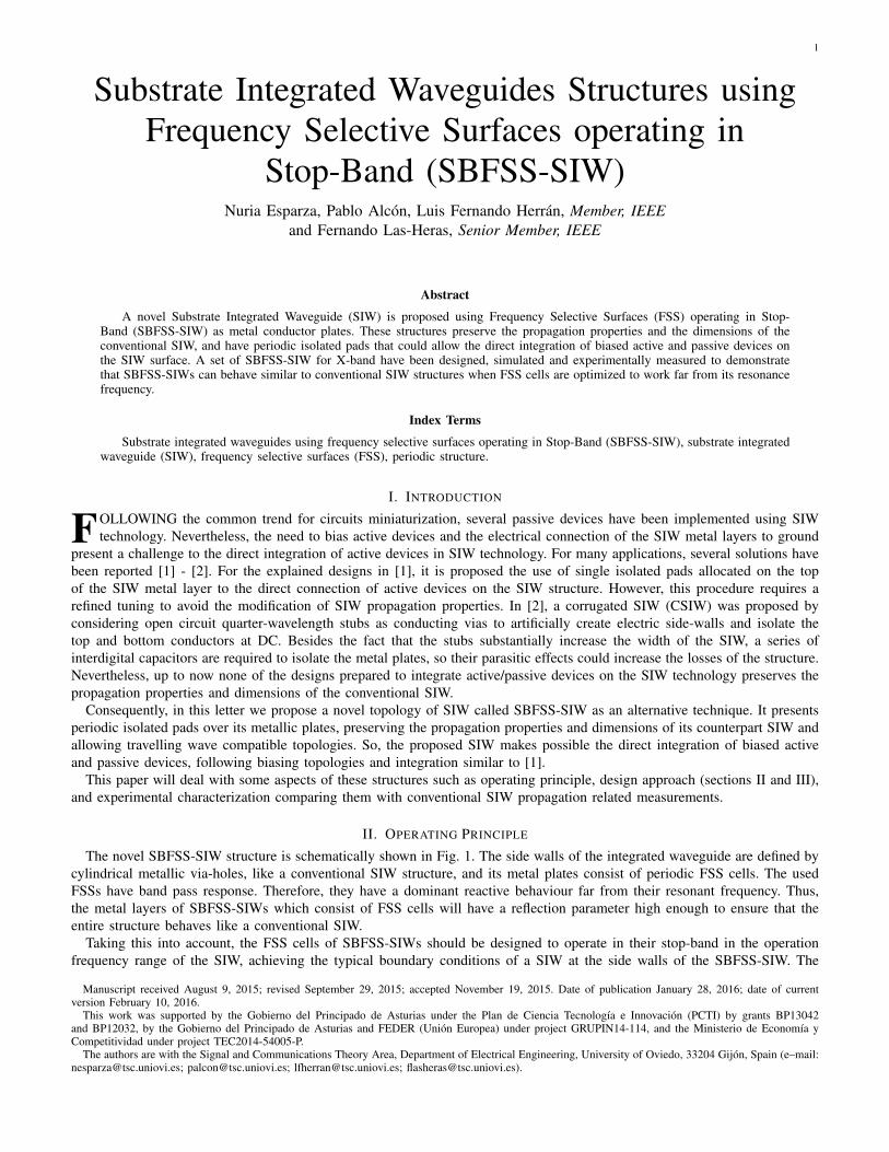
The novel SBFSS-SIW structure is schematically shown in Fig. 1. The side walls of the integrated waveguide are defined bycylindrical metallic via-holes, like a conventional SIW structure, and its metal plates consist of periodic FSS cells. The usedFSSs have band pass response. Therefore, they have a dominant reactive behaviour far from their resonant frequency. Thus,the metal layers of SBFSS-SIWs which consist of FSS cells will have a reflection parameter high enough to ensure that theentire structure behaves like a conventional SIW.
Taking this into account, the FSS cells of SBFSS-SIWs should be designed to operate in their stop-band in the operationfrequency range of the SIW, achieving the typical boundary conditions of a SIW at the side walls of the SBFSS-SIW. The
Manuscript received August 9, 2015; revised September 29, 2015; accepted November 19, 2015. Date of publication January 28, 2016; date of currentversion February 10, 2016.
This work was supported by the Gobierno del Principado de Asturias under the Plan de Ciencia Tecnologıa e Innovacion (PCTI) by grants BP13042and BP12032, by the Gobierno del Principado de Asturias and FEDER (Union Europea) under project GRUPIN14-114, and the Ministerio de Economıa yCompetitividad under project TEC2014-54005-P.
The authors are with the Signal and Communications Theory Area, Department of Electrical Engineering, University of Oviedo, 33204 Gijon, Spain (e–mail:[email protected]; [email protected]; [email protected]; [email protected]).
2
(a) (b) (c)
Fig. 1. Schematic of the proposed SBFSS-SIW structures (examples with single circle loops). (a) FSS cells allocated in top and bottom metal layers. (b) FSScells in top layer. (c) FSS cells in bottom layer. (In color)
equations presented in [3] can be used just to determine the starting value for designing FSSs, but the final element dimensionsneed to be fine-tuned to meet the desired frequency response.
This novel topology has the same propagation properties as its SIW counterpart, so the TE10 mode continues being thedominant mode of these new structures, as it is shown in section IV.
III. DESIGN
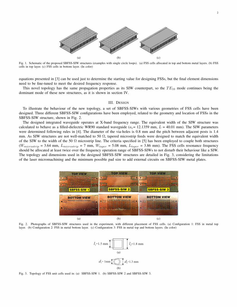
To illustrate the behaviour of the new topology, a set of SBFSS-SIWs with various geometries of FSS cells have beendesigned. Three different SBFSS-SIW configurations have been employed, related to the geometry and location of FSSs in theSBFSS-SIW structure, shown in Fig. 2.
The designed integrated waveguide operates at X-band frequency range. The equivalent width of the SIW structure wascalculated to behave as a filled-dielectric WR90 standard waveguide (ae= 12.1359 mm, L = 40.01 mm). The SIW parameterswere determined following rules in [4]. The diameter of the via-holes is 0.8 mm and the pitch between adjacent posts is 1.4mm. As SIW structures are not well-matched to 50 Ω, tapered microstrip feeds were designed to match the equivalent widthof the SIW to the width of the 50 Ω microstrip line. The criteria specified in [5] has been employed to couple both structures(Wmicrostrip = 3.64 mm, Lmicrostrip = 7 mm, Wtaper = 5.08 mm, Ltaper = 3.86 mm). The FSS cells resonance frequencyshould be allocated at least twice over the frequency operation range of SBFSS-SIWs to not disturb their behaviour like a SIW.The topology and dimensions used in the designed SBFSS-SIW structures are detailed in Fig. 3, considering the limitationsof the laser micromachining and the minimum possible pad size to add external circuits on SBFSS-SIW metal plates.
SBFSS SIW- 1
TOP VIEW
BOTTOM VIEW
(a)
SBFSS SIW- 2
TOP VIEW
BOTTOM VIEW
(b)
SBFSS SIW- 3
TOP VIEW
BOTTOM VIEW
(c)
Fig. 2. Photographs of SBFSS-SIW structures used in the experiment, with different placement of FSS cells. (a) Configuration 1: FSS in metal toplayer. (b) Configuration 2: FSS in metal bottom layer. (c) Configuration 3: FSS in metal top and bottom layers. (In color)
l1=1.5 mm l
2=1.8 mm
(a)
d1= 1mm d
2=1.3 mm
(b)
Fig. 3. Topology of FSS unit cells used in: (a) SBFSS-SIW 1. (b) SBFSS-SIW 2 and SBFSS-SIW 3.
3
IV. SIMULATED AND EXPERIMENTAL RESULTS
To show that SBFSS-SIWs have similar propagation characteristics as SIWs, a comparison of the E-field distribution andS-parameters is presented. A standard 60 mil RO4003C substrate was used in all the manufactured structures. The library-defined HFSS model for this substrate was used to carry out the simulations. A custom microstrip TRL was used to calibratethe VNA, in order to avoid parasitics effects in the connectors used. The design of this element follows common rules in thiskind of standard.
SIW
(a)
SBFSS-SIW 1 SBFSS-SIW 2 SBFSS-SIW 3
(b)
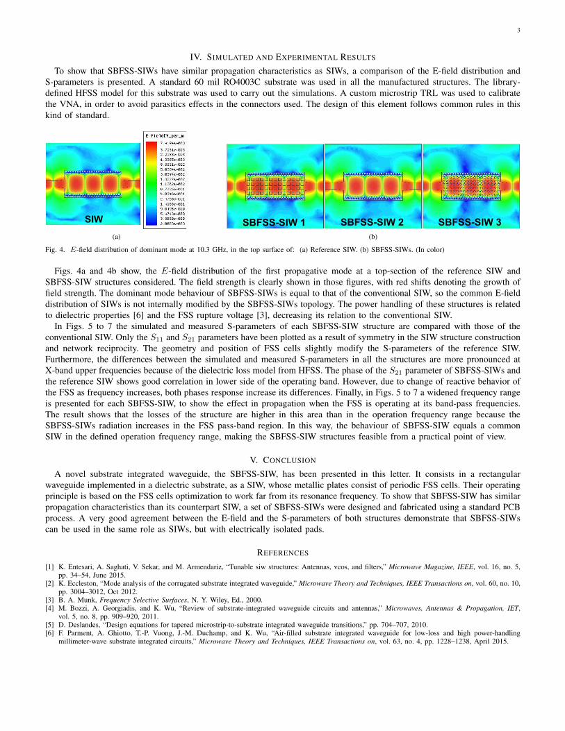
Fig. 4. E-field distribution of dominant mode at 10.3 GHz, in the top surface of: (a) Reference SIW. (b) SBFSS-SIWs. (In color)
Figs. 4a and 4b show, the E-field distribution of the first propagative mode at a top-section of the reference SIW andSBFSS-SIW structures considered. The field strength is clearly shown in those figures, with red shifts denoting the growth offield strength. The dominant mode behaviour of SBFSS-SIWs is equal to that of the conventional SIW, so the common E-fielddistribution of SIWs is not internally modified by the SBFSS-SIWs topology. The power handling of these structures is relatedto dielectric properties [6] and the FSS rupture voltage [3], decreasing its relation to the conventional SIW.
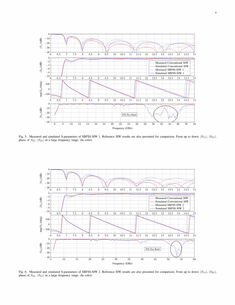
In Figs. 5 to 7 the simulated and measured S-parameters of each SBFSS-SIW structure are compared with those of theconventional SIW. Only the S11 and S21 parameters have been plotted as a result of symmetry in the SIW structure constructionand network reciprocity. The geometry and position of FSS cells slightly modify the S-parameters of the reference SIW.Furthermore, the differences between the simulated and measured S-parameters in all the structures are more pronounced atX-band upper frequencies because of the dielectric loss model from HFSS. The phase of the S21 parameter of SBFSS-SIWs andthe reference SIW shows good correlation in lower side of the operating band. However, due to change of reactive behavior ofthe FSS as frequency increases, both phases response increase its differences. Finally, in Figs. 5 to 7 a widened frequency rangeis presented for each SBFSS-SIW, to show the effect in propagation when the FSS is operating at its band-pass frequencies.The result shows that the losses of the structure are higher in this area than in the operation frequency range because theSBFSS-SIWs radiation increases in the FSS pass-band region. In this way, the behaviour of SBFSS-SIW equals a commonSIW in the defined operation frequency range, making the SBFSS-SIW structures feasible from a practical point of view.
V. CONCLUSION
A novel substrate integrated waveguide, the SBFSS-SIW, has been presented in this letter. It consists in a rectangularwaveguide implemented in a dielectric substrate, as a SIW, whose metallic plates consist of periodic FSS cells. Their operatingprinciple is based on the FSS cells optimization to work far from its resonance frequency. To show that SBFSS-SIW has similarpropagation characteristics than its counterpart SIW, a set of SBFSS-SIWs were designed and fabricated using a standard PCBprocess. A very good agreement between the E-field and the S-parameters of both structures demonstrate that SBFSS-SIWscan be used in the same role as SIWs, but with electrically isolated pads.
REFERENCES
[1] K. Entesari, A. Saghati, V. Sekar, and M. Armendariz, “Tunable siw structures: Antennas, vcos, and filters,” Microwave Magazine, IEEE, vol. 16, no. 5,pp. 34–54, June 2015.
[2] K. Eccleston, “Mode analysis of the corrugated substrate integrated waveguide,” Microwave Theory and Techniques, IEEE Transactions on, vol. 60, no. 10,pp. 3004–3012, Oct 2012.
[3] B. A. Munk, Frequency Selective Surfaces, N. Y. Wiley, Ed., 2000.[4] M. Bozzi, A. Georgiadis, and K. Wu, “Review of substrate-integrated waveguide circuits and antennas,” Microwaves, Antennas & Propagation, IET,
vol. 5, no. 8, pp. 909–920, 2011.[5] D. Deslandes, “Design equations for tapered microstrip-to-substrate integrated waveguide transitions,” pp. 704–707, 2010.[6] F. Parment, A. Ghiotto, T.-P. Vuong, J.-M. Duchamp, and K. Wu, “Air-filled substrate integrated waveguide for low-loss and high power-handling
millimeter-wave substrate integrated circuits,” Microwave Theory and Techniques, IEEE Transactions on, vol. 63, no. 4, pp. 1228–1238, April 2015.
4
6 6.5 7 7.5 8 8.5 9 9.5 10 10.5 11 11.5 12 12.5 13 13.5 14 14.5 15−10−8−6−4−20
|S21|(d
B) Measured Conventional SIW
Simulated Conventional SIWMeasured SBFSS-SIW 1Simulated SBFSS-SIW 1
6 6.5 7 7.5 8 8.5 9 9.5 10 10.5 11 11.5 12 12.5 13 13.5 14 14.5 15−40−30−20−10
0
|S11|(d
B)
6 6.5 7 7.5 8 8.5 9 9.5 10 10.5 11 11.5 12 12.5 13 13.5 14 14.5 15
−1000
100
ang(S21)(
deg)
6 8 10 12 14 16 18 20 22 24 26 28 30 32 34 36 38 40−40−30−20−10
0
FSS Pass-Band
Frequency (GHz)
|S21|(d
B)
Fig. 5. Measured and simulated S-parameters of SBFSS-SIW 1. Reference SIW results are also presented for comparison. From up to down: |S11|, |S21|,phase of S21, |S21| in a large frequency range. (In color)
6 6.5 7 7.5 8 8.5 9 9.5 10 10.5 11 11.5 12 12.5 13 13.5 14 14.5 15−10−8−6−4−20
|S21|(d
B) Measured Conventional SIW
Simulated Conventional SIWMeasured SBFSS-SIW 2Simulated SBFSS-SIW 2
6 6.5 7 7.5 8 8.5 9 9.5 10 10.5 11 11.5 12 12.5 13 13.5 14 14.5 15−40−30−20−10
0
|S11|(d
B)
6 6.5 7 7.5 8 8.5 9 9.5 10 10.5 11 11.5 12 12.5 13 13.5 14 14.5 15
−1000
100
ang(S21)(
deg)
5 10 15 20 25 30 35 40 45 50 55 60−40−30−20−10
0
FSS Pass-Band
Frequency (GHz)
|S21|(d
B)
Fig. 6. Measured and simulated S-parameters of SBFSS-SIW 2. Reference SIW results are also presented for comparison. From up to down: |S11|, |S21|,phase of S21, |S21| in a large frequency range. (In color)

5
6 6.5 7 7.5 8 8.5 9 9.5 10 10.5 11 11.5 12 12.5 13 13.5 14 14.5 15−10−8−6−4−20
|S21|(d
B) Measured Conventional SIW
Simulated Conventional SIWMeasured SBFSS-SIW 3Simulated SBFSS-SIW 3
6 6.5 7 7.5 8 8.5 9 9.5 10 10.5 11 11.5 12 12.5 13 13.5 14 14.5 15−40−30−20−10
0
|S11|(d
B)
6 6.5 7 7.5 8 8.5 9 9.5 10 10.5 11 11.5 12 12.5 13 13.5 14 14.5 15
−1000
100
ang(S21)(
deg)
6 8 10 12 14 16 18 20 22 24 26 28 30 32 34 36 38 40 42 44−30
−20
−10
0
FSS Pass-Band
Frequency (GHz)
|S21|(d
B)
Fig. 7. Measured and simulated S-parameters of SBFSS-SIW 3. Reference SIW results are also presented for comparison. From up to down: |S11|, |S21|,phase of S21, |S21| in a large frequency range. (In color)