Embed Size (px)
Citation preview

1
Thin Resist film Processing issues
Ioannis RaptisPatterning GroupInstitute of MicroelectronicsNational Center for Scientific Reasearch ‘Demokritos’15310 Ag. Paraskevi Attikis, GreeceE-mail: [email protected]://imel.demokritos.gr
ContentsGlass transition changes in thin resist filmsEtching rate of thin resist filmsDissolution properties of thin resist films
SW-OPTI methodology / Results
)4
cos(222
nd
BABAI oooos
C.D.Diakoumakos, I.Raptis Polymer 44 251(2003) D.Niakoula, I.Raptis, D.Goustouridis, P.Argitis Jpn. J. Appl. Phys. 43 (5247)2004
Interference Equation
Operation Principle
Parameters affecting Tg
film
film thicknessfilm – substrate interactionscoating methoddistribution of molecules
At glass transitionSpecific volumeRefractive indexSurface roughnesschange Exposure layout
50 m rectangular pads

Tgfilm values of AZ-EM materials
MMC2 Bulk T=400nm 10%w/w 130oC,1min
138 134
MMC4 Bulk T=640nm 10%w/w 120oC, 1min
T=152nm 2%w/w 150oC, 1min
154.9 142 138
MMC13 Bulk T=42nm 4%w/w conc. 120oC,1min
T=276nm 10%w/w conc 120oC,1min
T=285nm 10%w/w conc 90oC,1m
128.7 146 114 115
Bulk T=40nm 4%w/w conc 120oC,1min
T=258nm 10%w/w conc 120oC,1min
MMC14 132.7 146 120
Bulk T=44nm 4%w/w conc. 120oC,1min
T=335nm 10%w/w conc 120oC,1min
MMC15 131.2 142 117
MMC13: terpolymer Mw: 30000MMC14: terpolymer Mw: 14000MMC15: terpolymer Mw: 45000
0.53
0.54
0.55
0.56
0.57
0.58
0.59
0.60
0.61
60 80 100 120 140 160 180
Temperature (oC)
Inte
rfer
ence
Sig
nal (
a.u.
)
MMC13-4%-120C1min
MMC14-4%-120C1min

MW-OPTI interferometry method / Results
Specifications:Real time calculation of polymeric film thicknessControlled heating and cooling rateControlled atmosphere (humidity level)Results:Evaluation of Tg
film for films down to 50nm
60 80 100 120 140 160 180 200100.0
100.5
101.0
101.5
102.0
102.5
103.0
103.5
TH
ICK
NE
SS
(n
m)
TEMPERATURE (oC)
100nm pmma_500sec exposure
115 oC
141 oC
0 500 1000 1500 2000 2500 3000 3500 4000
96
98
100
102
104
106
108
110
112
114
116
118
120
BroadBand DUV Exposure Time (sec)
Tgfil
m (
o C)
Thin exposed PMMA resist

•Etch Rate is decreasing as the initial film thickness declines
•For initial thicknesses >150nm ER gets its bulk value
•ERbulk – ERthickn~50nm>20nm/min
•Relative decrease of about 20% depending on the polymer
Increased etch resistance of thin polymeric filmsPossible explanations for this are based on the effect of:•Sample heating (during process)•Physical properties of polymer (Free volume, Density, Diffusivity)
0 100 200 300 400 500 600 700
100
120
140
160
180
200
220
240
GKRS PHEMA PMMA
Etc
h R
ate
(nm
/min
)
Initial Polymer Thickness (nm)
Etch Rate vs. initial thickness
N.Vourdas, A.G.Boudouvis, E.Gogolides Microelec. Eng. 78, 474(2005)
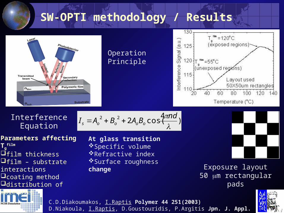
Multi Wavelength Dissolution Rate Monitor
Characteristics•Low-Moderate sampling Rate (<50samples/sec)•Need for fitting•Applicable to very thin films (>40nm)•Allows detailed study of swelling
Spectrometer
A.Kokkinis, E.S.Valamontes, I.Raptis J. Physics (2005) “Dissolution properties of ultrathin photoresist films for the fabrication of nanostructures”
Dissolution behaviour depends on film thicknessDissolution behaviour depends on film thickness Effect of Molecular Weight on dissolutionEffect of Molecular Weight on dissolution
0
0.1
0.2
0.3
0.4
0.5
0.6
0.7
0.8
0.9
1
0 50 100 150Development time (sec)
No
rma
lize
d T
hic
kn
es
sMMC13-10%
MMC14-10%
MMC15-10%
Conclusions / Future Plans
Conclusions•Non destructive Optical methodologies were developed for the in-situ monitoring of the thin film properties.•Tg
film in case of thin films are different from the bulk ones. Exposed and unexposed areas present different properties•Dissolution of thin films was studied. Results depend on the polymer/resist material.•Thin film issues are important for the sub 45nm nodes
Future Plans•Comparison of the three available optical methodologies for the Tg
film calculation.•Development processing conditions effect on the development rate of thin films•Thermal processing (PAB, PEB) effects on polymer/resist properties in the case of thin films