Embed Size (px)
DESCRIPTION
pwm inverter electronic info
Citation preview

EE362L, Power Electronics, PWM Inverter Control Circuit Version Feb. 20, 2008
Page 1 of 34
Introduction Unipolar PWM inverters (also known as Class D or switching amplifiers) efficiently amplify a small input signal Vcont . The output voltage to the load is either +Vdc, –Vdc, or zero, depending on whether Vcont and –Vcont are greater or smaller than a reference triangle wave Vtri. The output load voltage contains a replica of Vcont , and also strong harmonics centered about even multiples of mf, where mf is the ratio of the reference triangle wave frequency with
respect to the frequency of Vcont. , i.e, cont
trif f
fm = .
The amplifier operates on the principle of comparing Vcont (and –Vcont) to a reference triangle wave Vtri . This principle is illustrated in Figure 1. The illustration given has ma = 0.9, where ma is the ratio of peak control voltage to peak triangle voltage. The logic used to operate the four switches in the H-Bridge configuration of Figure 2 is as follows:
Vcont > Vtri , close switch A+, open switch A– , so voltage Va = Vdc
Vcont < Vtri , open switch A+, close switch A– , so voltage Va = 0 –Vcont > Vtri , close switch B+, open switch B– , so voltage Vb = Vdc
–Vcont < Vtri , open switch B+, close switch B– , so voltage Vb = 0
Figure 1. Vcont , –Vcont , and Vtri
Vcont –Vcont Vtri

EE362L, Power Electronics, PWM Inverter Control Circuit Version Feb. 20, 2008
Page 2 of 34
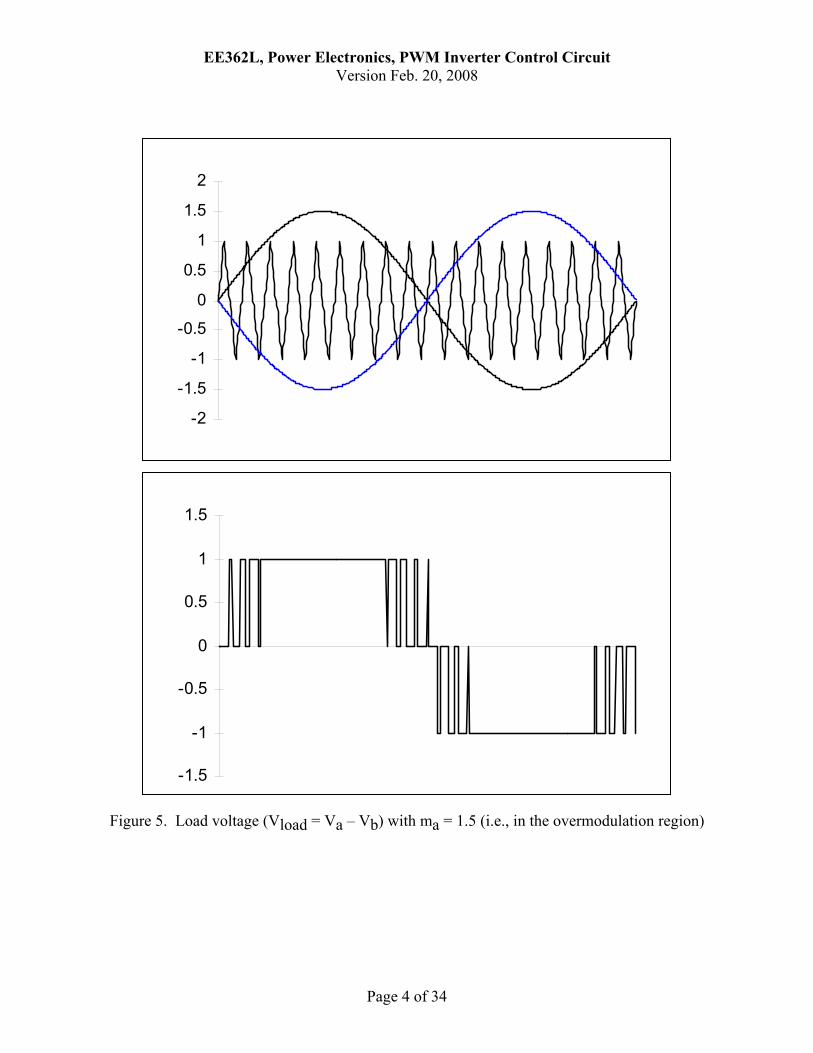
The resulting load voltage is shown in Figure 3. (Note – see the Appendix for a more complete graphical development of Figure 3). The harmonics in this waveform are high-frequency side bands 2kftri ± fcont, 2kftri ±3fcont, 2kftri ±5fcont, and so forth, for k = 1, 2, 3, …), where ftri is the frequency of the triangular wave, and fcont is the frequency of Vcont. Waveforms for ma = 0.5 and 1.5 are shown in Figures 4 and 5. The magnitudes of the load voltage frequency components, taken from [1], are shown in Table 1. For small ma, many of these values are large in relation to the fundamental. However, as long as mf is large, the undesired high frequency components are relatively easy to filter at the load, so that the output load voltage resembles Vcont reasonably well.
Figure 3. Load voltage (Vload = Va – Vb) with ma = 0.9 (i.e., in the linear region)
Figure 2. Four MOSFET switches configured as an H-Bridge (note that the MOSFET source nodes are not all at the same potential, thus requiring
isolated firing circuits for A+ and B+)
30-40Vdc
A+ B+
A– B– +Vload –
Freewheeling diodes (optional in this circuit because the MOSFETS used have adequate internal reverse diodes) High-frequency capacitor to provide ripple current from DC source
+ Va –
+ Vb –
Vload = Va – Vb
a b

EE362L, Power Electronics, PWM Inverter Control Circuit Version Feb. 20, 2008
Page 3 of 34
Figure 4. Load voltage (Vload = Va – Vb) with ma = 0.5 (i.e., in the linear region)
-1.5
-1
-0.5
0
0.5
1
1.5
-1.5
-1
-0.5
0
0.5
1
1.5
EE362L, Power Electronics, PWM Inverter Control Circuit Version Feb. 20, 2008
Page 4 of 34
Figure 5. Load voltage (Vload = Va – Vb) with ma = 1.5 (i.e., in the overmodulation region)
-2
-1.5
-1
-0.5
0
0.5
1
1.5
2
-1.5
-1
-0.5
0
0.5
1
1.5
EE362L, Power Electronics, PWM Inverter Control Circuit Version Feb. 20, 2008
Page 5 of 34
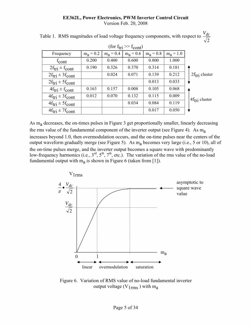
Table 1. RMS magnitudes of load voltage frequency components, with respect to 2
dcV
(for ftri >> fcont) Frequency ma = 0.2 ma = 0.4 ma = 0.6 ma = 0.8 ma = 1.0
fcont 0.200 0.400 0.600 0.800 1.000
2ftri ± fcont 0.190 0.326 0.370 0.314 0.181
2ftri ± 3fcont 0.024 0.071 0.139 0.212
2ftri ± 5fcont 0.013 0.033
4ftri ± fcont 0.163 0.157 0.008 0.105 0.068
4ftri ± 3fcont 0.012 0.070 0.132 0.115 0.009
4ftri ± 5fcont 0.034 0.084 0.119
4ftri ± 7fcont 0.017 0.050
As ma decreases, the on-times pulses in Figure 3 get proportionally smaller, linearly decreasing the rms value of the fundamental component of the inverter output (see Figure 4). As ma increases beyond 1.0, then overmodulation occurs, and the on-time pulses near the centers of the output waveform gradually merge (see Figure 5). As ma becomes very large (i.e., 5 or 10), all of the on-time pulses merge, and the inverter output becomes a square wave with predominantly low-frequency harmonics (i.e., 3rd, 5th, 7th, etc.). The variation of the rms value of the no-load fundamental output with ma is shown in Figure 6 (taken from [1]).
Figure 6. Variation of RMS value of no-load fundamental inverter output voltage (V1rms ) with ma
ma 0 1
V1rms
2dcV
24 dcV•
π
linear overmodulation saturation
asymptotic to square wave value
2ftri cluster
4ftri cluster
EE362L, Power Electronics, PWM Inverter Control Circuit Version Feb. 20, 2008
Page 6 of 34
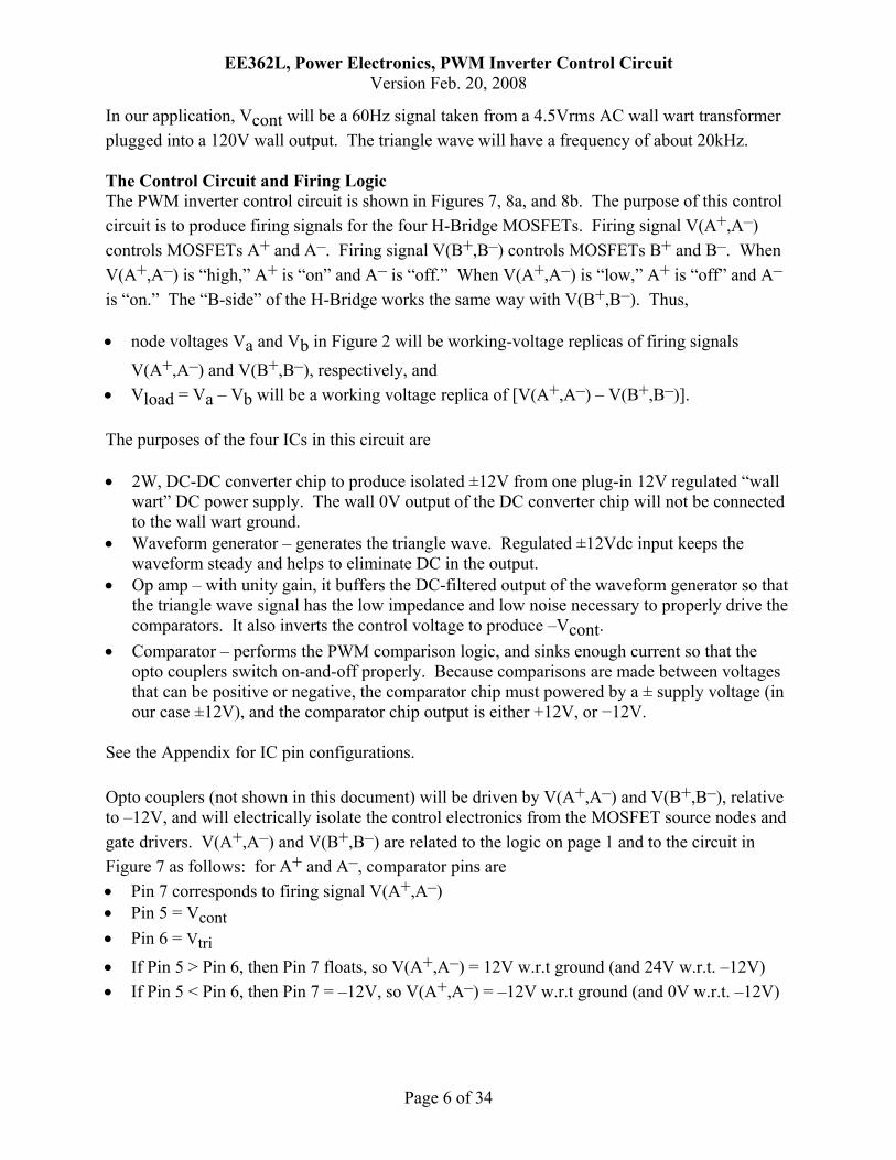
In our application, Vcont will be a 60Hz signal taken from a 4.5Vrms AC wall wart transformer plugged into a 120V wall output. The triangle wave will have a frequency of about 20kHz. The Control Circuit and Firing Logic The PWM inverter control circuit is shown in Figures 7, 8a, and 8b. The purpose of this control circuit is to produce firing signals for the four H-Bridge MOSFETs. Firing signal V(A+,A–) controls MOSFETs A+ and A–. Firing signal V(B+,B–) controls MOSFETs B+ and B–. When V(A+,A–) is “high,” A+ is “on” and A– is “off.” When V(A+,A–) is “low,” A+ is “off” and A– is “on.” The “B-side” of the H-Bridge works the same way with V(B+,B–). Thus, • node voltages Va and Vb in Figure 2 will be working-voltage replicas of firing signals
V(A+,A–) and V(B+,B–), respectively, and • Vload = Va – Vb will be a working voltage replica of [V(A+,A–) – V(B+,B–)]. The purposes of the four ICs in this circuit are • 2W, DC-DC converter chip to produce isolated ±12V from one plug-in 12V regulated “wall
wart” DC power supply. The wall 0V output of the DC converter chip will not be connected to the wall wart ground.
• Waveform generator – generates the triangle wave. Regulated ±12Vdc input keeps the waveform steady and helps to eliminate DC in the output.
• Op amp – with unity gain, it buffers the DC-filtered output of the waveform generator so that the triangle wave signal has the low impedance and low noise necessary to properly drive the comparators. It also inverts the control voltage to produce –Vcont.
• Comparator – performs the PWM comparison logic, and sinks enough current so that the opto couplers switch on-and-off properly. Because comparisons are made between voltages that can be positive or negative, the comparator chip must powered by a ± supply voltage (in our case ±12V), and the comparator chip output is either +12V, or −12V.
See the Appendix for IC pin configurations. Opto couplers (not shown in this document) will be driven by V(A+,A–) and V(B+,B–), relative to –12V, and will electrically isolate the control electronics from the MOSFET source nodes and gate drivers. V(A+,A–) and V(B+,B–) are related to the logic on page 1 and to the circuit in Figure 7 as follows: for A+ and A–, comparator pins are • Pin 7 corresponds to firing signal V(A+,A–) • Pin 5 = Vcont • Pin 6 = Vtri • If Pin 5 > Pin 6, then Pin 7 floats, so V(A+,A–) = 12V w.r.t ground (and 24V w.r.t. –12V) • If Pin 5 < Pin 6, then Pin 7 = –12V, so V(A+,A–) = –12V w.r.t ground (and 0V w.r.t. –12V)

EE362L, Power Electronics, PWM Inverter Control Circuit Version Feb. 20, 2008
Page 7 of 34
0.01µF (freq. control)
(For control electronics wiring with solid #22 wire, use green for ground, red for
+12Vdc, violet for –12Vdc, and blue for all others)
Figure 7. PWM inverter control circuit (note – be sure to use the wiring color code to
make troubleshooting easier)
8 5 Op Amp 1 4
500Ω trimmer
14 8 Waveform Gen.
1 7
1kΩ
1kΩ
0.01µF 100kΩ
Approx 22kHz triangle wave
Filtered and buffered
triangle wave
High-pass filter to block DC
8 5 Comp
1 4
1.5kΩ, ½W
270kΩ
1.5kΩ, ½W
1kΩ
1kΩ
270kΩ
+12Vdc regulated from 2W, DC converter chip
–12Vdc regulated from
2W, DC converter chip
V(A+,A–) V(B+,B–)
Vcont
Vcont
red
green
blue
blue
blue
violet
blue
violet
violet
violet
green
red
red
green
These ½W resistors can get hot - keep them off the surface of the protoboard
10kΩ 9.53kΩ
1kΩ trimmer
–Vcont blue
Vcont
60Hz AC signal from AC wall wart and 500Ω potentiometer
Protoboard common connected to 0V output pin 2W, DC converter chipSee Appendix for IC pin configurations
green

EE362L, Power Electronics, PWM Inverter Control Circuit Version Feb. 20, 2008
Page 8 of 34
Protoboard common (i.e., the green wires) (protoboard common is the 0V output pin on the DC converter chip, and is not
connected to the wall wart ground)
Figure 8a. The 16” long piece of 1” x 10” wood piece with inverter control circuit mounted in the lower 4”
Jack for AC wall wart, with 0.1µF capacitor
Jack for DC wall wart, with 0.1µF capacitor
–12Vdc isolated rail
+12Vdc isolated rail
2W, DC-DC converter
500Ω pot for adjusting
Vcont
You will build this part the following
week
4”
EE362L, Power Electronics, PWM Inverter Control Circuit Version Feb. 20, 2008
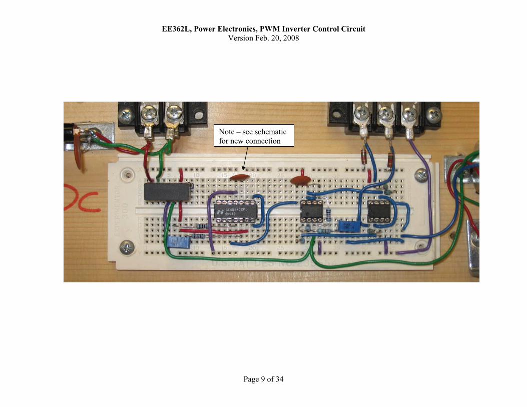
Page 9 of 34
Note – see schematic for new connection

EE362L, Power Electronics, PWM Inverter Control Circuit Version Feb. 20, 2008
Page 10 of 34
Note – see schematic for new connection

EE362L, Power Electronics, PWM Inverter Control Circuit Version Feb. 20, 2008
Page 11 of 34
For B+ and B–, the comparator pins are • Pin 1 corresponds to firing signal V(B+,B–) • Pin 3 = –Vcont • Pin 2 = Vtri • If Pin 3 > Pin 2, then Pin 1 floats, so V(B+,B–) = 12V w.r.t ground (and 24V w.r.t. –12V) • If Pin 3 < Pin 2, then Pin 1 = –12V, so V(B+,B–) = –12V w.r.t ground (and 0V w.r.t. –12V) The Experiment When checking out your circuit, make sure that each chip is receiving the proper +12V and −12V supply voltages. Do this using multimeter measurements directly at the appropriate pins on the chips.
Step 1 The Triangle Waveform Generator
1. The objective of Step 1 is to have the waveform generator portion of the circuit working
properly. Do not plug in either wall wart yet. Build your project on a 16” long piece of 1” x 10” wood, occupying only about the lower 4” inches of the wood. Carefully connect the DC wall wart jack (with 0.1µF ceramic capacitor), the 2W DC converter chip, and the waveform generator IC plus its supporting components and high-pass filter. Use the sockets provided. The 2W DC converter chip produces isolated ±12V, and its output ground (termed “protoboard common” here) is also electrically isolated from the ground terminal of the DC wall wart. To maintain isolation, the protoboard common must not be connected to the ground of the wall wart.
2. Perform the power supply wiring continuity check. With the wall wart disconnected, use a
multimeter to • Confirm that the ground terminal of the wall wart is isolated from the 0V output pin
of the DC converter chip. • Confirm that the 12V wall wart output terminal is isolated from the +12V output pin
of the DC converter chip. 3. Perform the following DC converter chip test. Connect the 12V wall wart so that the DC
converter chip is powering your circuit. Then,
• Check the +12V and −12V output voltages of the DC converter chip. If either drops more than 0.5V from nominal, then your circuit is overloading the chip. In that case, you likely have a wiring short circuit, other wiring problem, or possibly a failed component. Unplug the wall wart, debug, and fix the problem before proceeding. Overloading the DC converter chip will cause it to overheat and fail.

EE362L, Power Electronics, PWM Inverter Control Circuit Version Feb. 20, 2008
Page 12 of 34
4. Using an oscilloscope, observe the output of the triangle-wave generator with respect to the
protoboard common. The triangle wave should have a frequency of approximately 22kHz (±15%) and max/min values of approximately ±4V. Note any DC offset by observing the maximum and minimum values (see Figure 9). Adjust the 500Ω trimmer potentiometer until the triangle wave has equal rise and fall times (see Figure 10). To help make the determination, it is helpful to “single step” through oscilloscope snapshots.
Figure 9. Output of triangle-wave generator (with respect to protoboard common)
Indicates DC offset
Figure 10. Rise and fall times of the triangle wave
Equal rise and fall times
EE362L, Power Electronics, PWM Inverter Control Circuit Version Feb. 20, 2008
Page 13 of 34
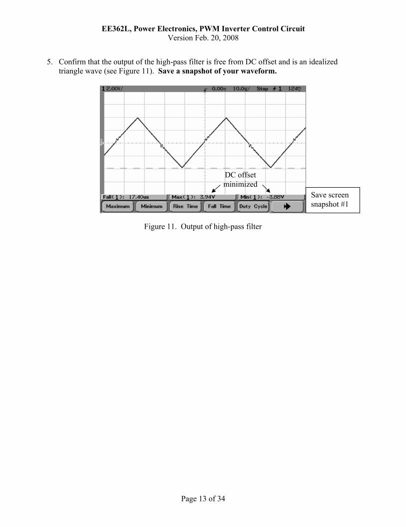
5. Confirm that the output of the high-pass filter is free from DC offset and is an idealized
triangle wave (see Figure 11). Save a snapshot of your waveform.
Figure 11. Output of high-pass filter
DC offset minimized
Save screen snapshot #1

EE362L, Power Electronics, PWM Inverter Control Circuit Version Feb. 20, 2008
Page 14 of 34
Step 2
Producing Vcont and –Vcont, and Testing the Comparators 6. Disconnect the DC wall wart, and then finish wiring the protoboard circuit. For Vcont, you
will use a 4.5Vrms AC wall wart and 500Ω potentiometer to adjust Vcont. Use a 0.1µF ceramic capacitor on the AC wall wart jack. It is important that you do not interchange the AC and DC wall warts! The AC wall warts are marked with yellow paint. But before connecting the AC wall wart, energize your circuit and confirm with an oscilloscope that both V(A+,A–) and V(B+,B–), with respect to protoboard –12V reference, are varying sharply from +24V to 0V. Both waveforms should have a 50% duty cycle. Save a simultaneous snapshot of the two waveforms. Expect to see the waveforms shown in Figure 12. Use your multimeter to confirm that your DC measurements are within a few tenths of a volt compared to those given alongside Figure 12.
7. Connect the AC wall wart, and raise the 500Ω Vcont potentiometer for maximum Vcont.
Use your oscilloscope to simultaneously view Vcont and –Vcont with respect to protoboard common. They should be 180° out of phase. Adjust the 1kΩ, –Vcont trimmer potentiometer so that –Vcont has the same rms magnitude as Vcont. With ma at the maximum, use a
multimeter to check AC voltage [V(A+,A–) – V(B+,B–)]. Expect about 21Vac. 8. Lower the 500Ω Vcont potentiometer for minimum Vcont. Move the oscilloscope probes
back to observe V(A+,A–) and V(B+,B–) with respect to protoboard –12V reference. Then, gradually raise the 500Ω Vcont potentiometer so that Vcont increases from zero to about 3Vrms. Note the variations in the two waveforms as Vcont increases. The two
Figure 12. Output control voltages V(A+,A–) and V(B+,B–), with respect to protoboard –12V reference, with Vcont = 0 (i.e., the ma = 0 case)
Save screen snapshot #2
For ma = 0, use a multimeter to check the following DC voltages with respect to –12V ref:
V(A+,A–) ≈ 11.8Vdc V(B+,B–) ≈ 11.8Vdc
EE362L, Power Electronics, PWM Inverter Control Circuit Version Feb. 20, 2008
Page 15 of 34
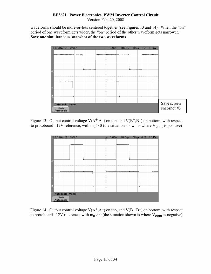
waveforms should be more-or-less centered together (see Figures 13 and 14). When the “on” period of one waveform gets wider, the “on” period of the other waveform gets narrower. Save one simultaneous snapshot of the two waveforms.
Figure 14. Output control voltage V(A+,A–) on top, and V(B+,B–) on bottom, with respect to protoboard –12V reference, with ma > 0 (the situation shown is where Vcont is negative)
Figure 13. Output control voltage V(A+,A–) on top, and V(B+,B–) on bottom, with respect to protoboard –12V reference, with ma > 0 (the situation shown is where Vcont is positive)
Save screen snapshot #3

EE362L, Power Electronics, PWM Inverter Control Circuit Version Feb. 20, 2008
Page 16 of 34
Step 3 Testing Idealized Load Voltage Vload = Va – Vb
9. Now, examine Figure 2. The firing circuit logic works as follows.
If V(A+,A–) is “high,” then
MOSFET A+ is on, MOSFET A– is off, and Va = Vdc. Else MOSFET A+ is off, MOSFET A– is on, and Va = 0.
End If If V(B+,B–) is “high,” then
MOSFET B+ is on, MOSFET B– is off, and Vb = Vdc. Else MOSFET B+ is off, MOSFET B– is on, and Vb = 0.
End If
To observe the idealized load voltage Vload = Va – Vb, do the following: • disconnect the Channel 2 probe from the oscilloscope, • connect the Channel 1 probe to V(A+,A–), and the ground clip of the Channel 1
probe to V(B+, B–), and • set the horizontal time scale to 5ms/division so you can see the 60Hz waveform.
Expect to see something similar to Figure 15, where ma is slightly greater than 1 so that the circuit is operating just into the overmodulation region. If necessary, adjust the 500Ω Vcont potentiometer until you see a waveform like that shown below. The “split” portion should be the same width in both half cycles. If not, adjust the op amp gain for –Vcont. until the splits have equal widths. Save a snapshot of your waveform.
Figure 15. Idealized Vload, with ma just into the overmodulation region
split
split Save screen snapshot #4

EE362L, Power Electronics, PWM Inverter Control Circuit Version Feb. 20, 2008
Page 17 of 34
10. Since the triangle wave frequency is more than 300 times higher than 60Hz, and furthermore
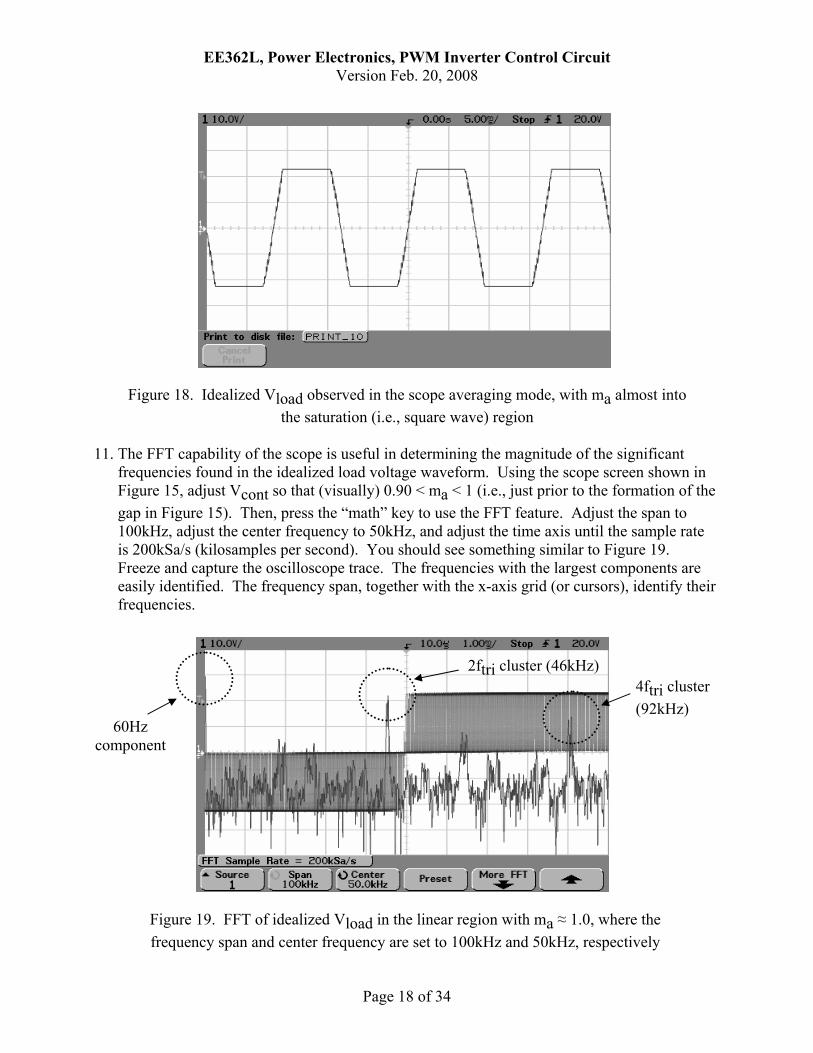
it is asynchronous with the 60Hz, the averaging feature of the oscilloscope can be used to remove most of the high frequency components and see the 60Hz component of the idealized Vload. While using the averaging feature, experiment by raising and lowering Vcont to observe the linear, overmodulation, and near-saturation regions. Expect to see waveforms similar to those in Figures 16, 17, and 18. Save a snapshot of your waveform with ma ≈ 1.
Figure 17. Idealized Vload observed in the scope averaging mode, with ma just into the overmodulation region
Figure 16. Idealized Vload observed in the scope averaging mode, with ma in the linear region
Save screen snapshot #5
EE362L, Power Electronics, PWM Inverter Control Circuit Version Feb. 20, 2008
Page 18 of 34
11. The FFT capability of the scope is useful in determining the magnitude of the significant
frequencies found in the idealized load voltage waveform. Using the scope screen shown in Figure 15, adjust Vcont so that (visually) 0.90 < ma < 1 (i.e., just prior to the formation of the gap in Figure 15). Then, press the “math” key to use the FFT feature. Adjust the span to 100kHz, adjust the center frequency to 50kHz, and adjust the time axis until the sample rate is 200kSa/s (kilosamples per second). You should see something similar to Figure 19. Freeze and capture the oscilloscope trace. The frequencies with the largest components are easily identified. The frequency span, together with the x-axis grid (or cursors), identify their frequencies.
Figure 18. Idealized Vload observed in the scope averaging mode, with ma almost into the saturation (i.e., square wave) region
Figure 19. FFT of idealized Vload in the linear region with ma ≈ 1.0, where the frequency span and center frequency are set to 100kHz and 50kHz, respectively
2ftri cluster (46kHz) 4ftri cluster (92kHz)
60Hz component

EE362L, Power Electronics, PWM Inverter Control Circuit Version Feb. 20, 2008
Page 19 of 34
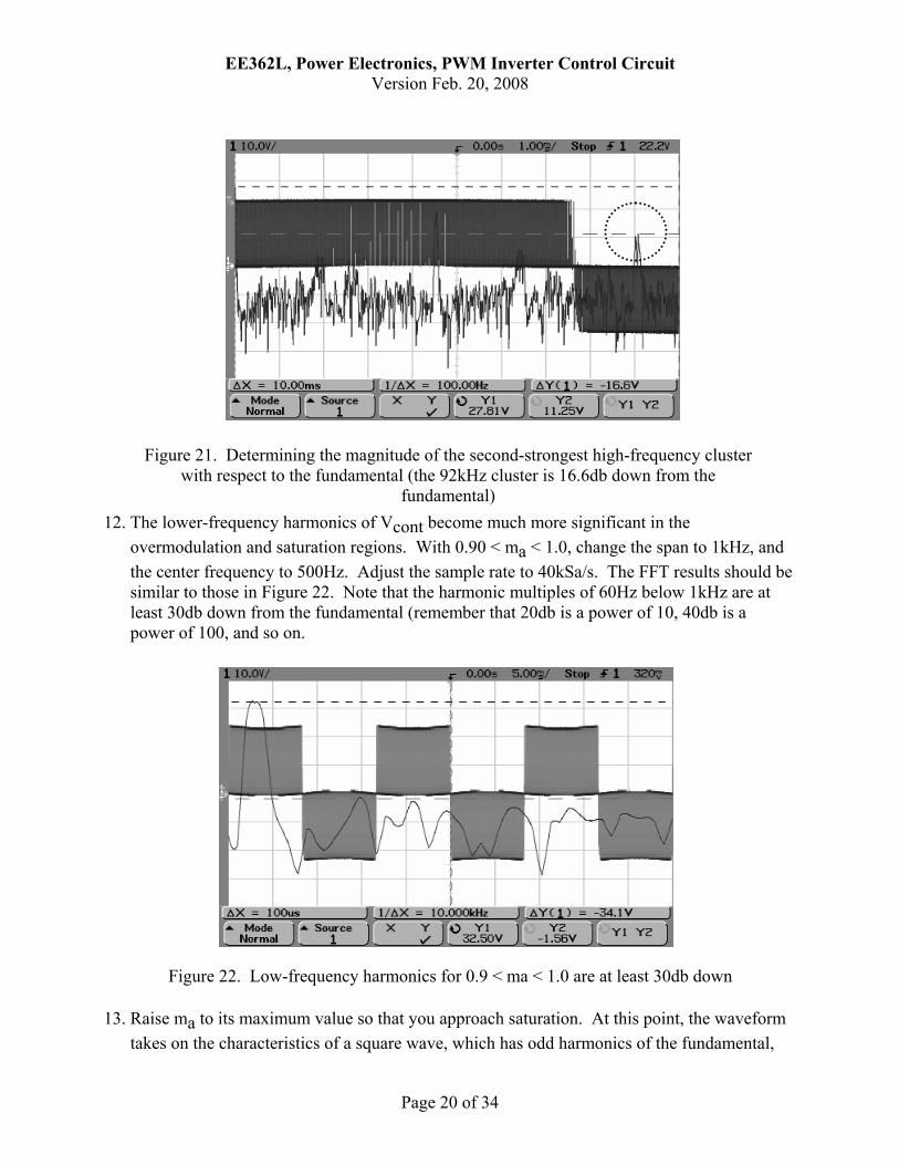
By pushing “More FFT” you can observe and adjust the db scale. If the db scale is 10db/division, while the voltage scale is 10V/division, then each scale volt corresponds to 1db. Use the cursors to measure the magnitude of the 2ftri cluster (i.e., approx. 46kHz) with respect to the 60Hz component (in scale volts). Save a snapshot of your waveform. Convert your volts to db. Then compute the ratio from the log10 relationship. For Figure 20, the computation yields
⎟⎟⎠
⎞⎜⎜⎝
⎛=−
Hz
kHzVV
db60
4610log2081.7 , so
⎟⎠⎞
⎜⎝⎛ −
= 2081.7
60
46 10Hz
kHzVV
= 0.31.
Compare your calculations to the values in Table 1.
Similarly, for the 4ftri cluster (i.e., approx. 92kHz), the values in Figure 21 yield
⎟⎟⎠
⎞⎜⎜⎝
⎛=−
Hz
kHzVV
db60
9210log206.16 , so
⎟⎠⎞
⎜⎝⎛ −
= 206.16
60
92 10Hz
kHzVV
= 0.148.
Compare your calculations to the values in Table 1.
Figure 20. Determining the magnitude of the strongest high-frequency cluster with respect to the fundamental (the 46kHz cluster is 7.81V (in dB) down from the
fundamental)
Save screen snapshot #6
EE362L, Power Electronics, PWM Inverter Control Circuit Version Feb. 20, 2008
Page 20 of 34
12. The lower-frequency harmonics of Vcont become much more significant in the
overmodulation and saturation regions. With 0.90 < ma < 1.0, change the span to 1kHz, and the center frequency to 500Hz. Adjust the sample rate to 40kSa/s. The FFT results should be similar to those in Figure 22. Note that the harmonic multiples of 60Hz below 1kHz are at least 30db down from the fundamental (remember that 20db is a power of 10, 40db is a power of 100, and so on.
13. Raise ma to its maximum value so that you approach saturation. At this point, the waveform
takes on the characteristics of a square wave, which has odd harmonics of the fundamental,
Figure 22. Low-frequency harmonics for 0.9 < ma < 1.0 are at least 30db down
Figure 21. Determining the magnitude of the second-strongest high-frequency cluster with respect to the fundamental (the 92kHz cluster is 16.6db down from the
fundamental)

EE362L, Power Electronics, PWM Inverter Control Circuit Version Feb. 20, 2008
Page 21 of 34
whose magnitudes decrease in proportion to harmonic order (i.e., the 3rd harmonic magnitude is 1/3 of the fundamental, and so on). Computations for Figures 23 and 24 show that the 3rd and 5th harmonic magnitudes are 0.30 and 0.13 of the fundamental, respectively.
Reference [1] N. Mohan, T. M. Undeland, W. P. Robbins, Power Electronics – Converters, Applications, and Design, 2nd Edition, John Wiley & Sons, Inc., 1995.
Figure 24. Near saturation, the 5th harmonic magnitude is 0.13 of the fundamental
Figure 23. Near saturation, the 3rd harmonic magnitude is 0.30 of the fundamental

EE362L, Power Electronics, PWM Inverter Control Circuit Version Feb. 20, 2008
Page 22 of 34
Parts List • Waveform Generator, Intersil ICL8038CCPD or NTE Electronics NTE864 (Mouser #570-
8038CCPD or #526-NTE864) • Dual Comparator, Fairchild LM393N (Mouser #512-LM393N) • Dual Op Amp, Texas Instruments TLE2072CP (Newark #08F9176, or Mouser #595-
TLE2072CP) • 14-pin DIP socket for the waveform generator • Two 8-pin DIP sockets (for the comparator and op amp) • 2W dual output DC-DC converter, SIP package, 12Vdc input, isolated ±12Vdc outputs, C&D
Technologies NMH1212SC (Mouser #580- NMH1212SC) • One 8-pin SIP socket for DC-DC converter, Mill-Max 310-93-108-41-001000 (Mouser
#575-193108) • Protoboard (large), Global Specialties EXP-300 (Newark #17C6898 or Mouser #510-103-
1300) • Two wall wart jacks (identical for both DC and AC) • Three 1” corner brackets (holes enlarged for wall wart jacks and 500Ω potentiometer) • One 2-terminal 20A terminal block • One 3-terminal 20A terminal block • 500Ω potentiometer, ½W, linear taper, 24mm, solder lugs, Alpha (Mouser #31VF205-F) • 500Ω, ½W, 3/8” square single-turn cermet trimmer potentiometers, Bourns 3386W-1-501
(Mouser 652-3386W-1-501-LF). These are marked 501 for 50•101 ohms. • 1kΩ, ½W, 3/8” square single-turn cermet trimmer potentiometers, Bourns 3386W-1-102
(Mouser 652-3386W-1-102-LF). These are marked 102 for 10•102 ohms. • 16” long piece of 1” by 10” wood • Two 1.5kΩ, ½W resistors (in student parts bin) • Two 270kΩ, ¼W resistors (in student parts bin) • Four 1kΩ, ¼W resistors (in student parts bin) • 10kΩ, ¼W resistor (in student parts bin) • 100kΩ, ¼W resistor (in student parts bin) • 9.53kΩ, ¼W resistor (in student parts bin) • Two 0.01µF, 100V ceramic disk capacitors (in student parts bin) Extra parts for the student parts bin and screw cabinet, at least • 5 of the dual comparators • 5 of the dual op amps • 5 of the wall wart jacks • 5 of the 500Ω square trimmer potentiometers • 5 of the 1kΩ square trimmer potentiometers • 5 of the 8-pin DIP sockets • 5 of the 14-pin DIP sockets • 5 of the 8-pin SIP sockets

EE362L, Power Electronics, PWM Inverter Control Circuit Version Feb. 20, 2008
Page 23 of 34
Extra parts (only for the TA parts bin), double those in the student parts bin, plus at least • 10 of the waveform generator chips • 10 of the 2W dual output DC-DC converter chips Plastic bags for parts • 4”x6”, 4mil antistatic for small parts • 8”x10”, 6mil for holding everything Other supplies in ENS212 • 4.5Vrms AC wall warts (marked with yellow paint), 2.1mm, Stancor STA-3545B (Newark
#84F2082)
EE362L, Power Electronics, PWM Inverter Control Circuit Version Feb. 20, 2008
Page 24 of 34
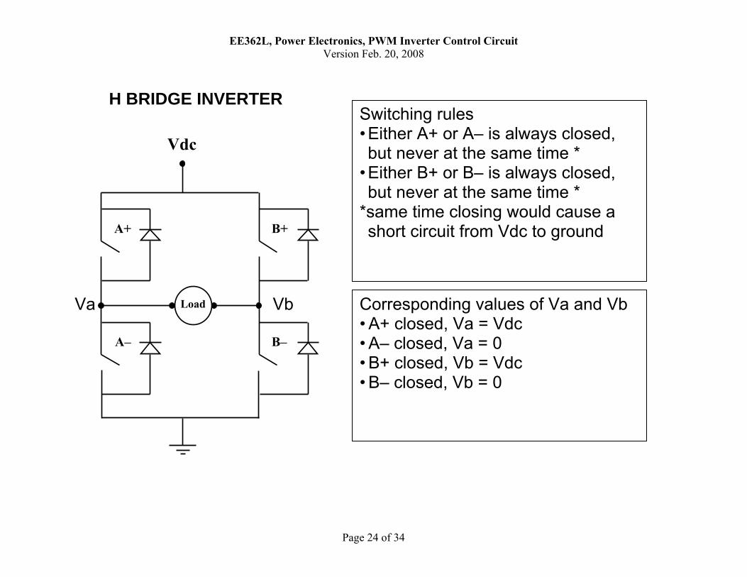
Switching rules • Either A+ or A– is always closed, but never at the same time *
• Either B+ or B– is always closed, but never at the same time *
*same time closing would cause a short circuit from Vdc to ground
Corresponding values of Va and Vb • A+ closed, Va = Vdc • A– closed, Va = 0 • B+ closed, Vb = Vdc • B– closed, Vb = 0
H BRIDGE INVERTER
Vdc
Load
A+ B+
A– B–
Va Vb

EE362L, Power Electronics, PWM Inverter Control Circuit Version Feb. 20, 2008
Page 25 of 34
Corresponding values of Vab •A+ closed and B– closed, Vab = Vdc •A+ closed and B+ closed, Vab = 0 •B+ closed and A– closed, Vab = –Vdc •B– closed and A– closed, Vab = 0
• The free wheeling diodes permit current to flow even if all switches did open
• These diodes also permit lagging currents to flow in inductive loads
Vdc
Load
A+ B+
A– B–
Va Vb
H BRIDGE INVERTER

EE362L, Power Electronics, PWM Inverter Control Circuit Version Feb. 20, 2008
Page 26 of 34
Figure 1. Vcont , –Vcont , and Vtri
Vcont –Vcont Vtri
But is a square wave output good enough? Not for us! Sinusoidal load voltage is usually the most desirable. But how do we approximate a
sinusoidal output with only three states (+Vdc, –Vdc, 0) ? The answer: Unipolar PWM modulation
Vcont > Vtri , close switch A+, open switch A– , so voltage Va = Vdc Vcont < Vtri , open switch A+, close switch A– , so voltage Va = 0 –Vcont > Vtri , close switch B+, open switch B– , so voltage Vb = Vdc –Vcont < Vtri , open switch B+, close switch B– , so voltage Vb = 0

EE362L, Power Electronics, PWM Inverter Control Circuit Version Feb. 20, 2008
Page 27 of 34
A+ closed, A– open, so Va in Figure 2 = Vdc. Else A– closed, A+ open, so Va in Figure 2 = 0.
B+ closed, B– open, so Vb in Figure 2 = Vdc. Else B– closed, B+ open, so Vb in Figure 2 = 0.
Va = Vdc
Va = 0 Vb = Vdc Vb = 0
EE362L, Power Electronics, PWM Inverter Control Circuit Version Feb. 20, 2008
Page 28 of 34
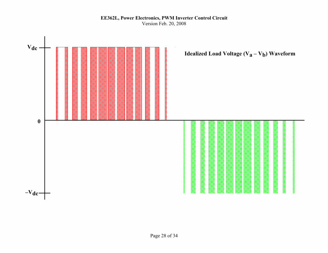
–Vdc
Idealized Load Voltage (Va – Vb) Waveform Vdc
0

EE362L, Power Electronics, PWM Inverter Control Circuit Version Feb. 20, 2008
Page 29 of 34
-1.5
-1
-0.5
0
0.5
1
1.5
-1.5
-1
-0.5
0
0.5
1
1.5
ma = 0.50 (linear region)
EE362L, Power Electronics, PWM Inverter Control Circuit Version Feb. 20, 2008
Page 30 of 34
-2
-1.5
-1
-0.5
0
0.5
1
1.5
2
-1.5
-1
-0.5
0
0.5
1
1.5
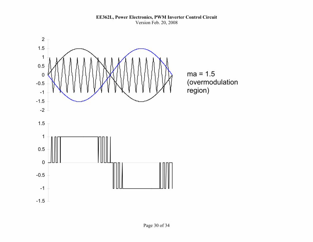
ma = 1.5 (overmodulation region)
EE362L, Power Electronics, PWM Inverter Control Circuit Version Feb. 20, 2008
Page 31 of 34
Vdc
Mot
A+ B+
A– B–
Vdc
Mot
A+ B+
A– B–
Vdc
Mot
A+ B+
A– B–
Vdc
Mot
A+ B+
A– B–
EE362L, Power Electronics, PWM Inverter Control Circuit Version Feb. 20, 2008
Page 32 of 34
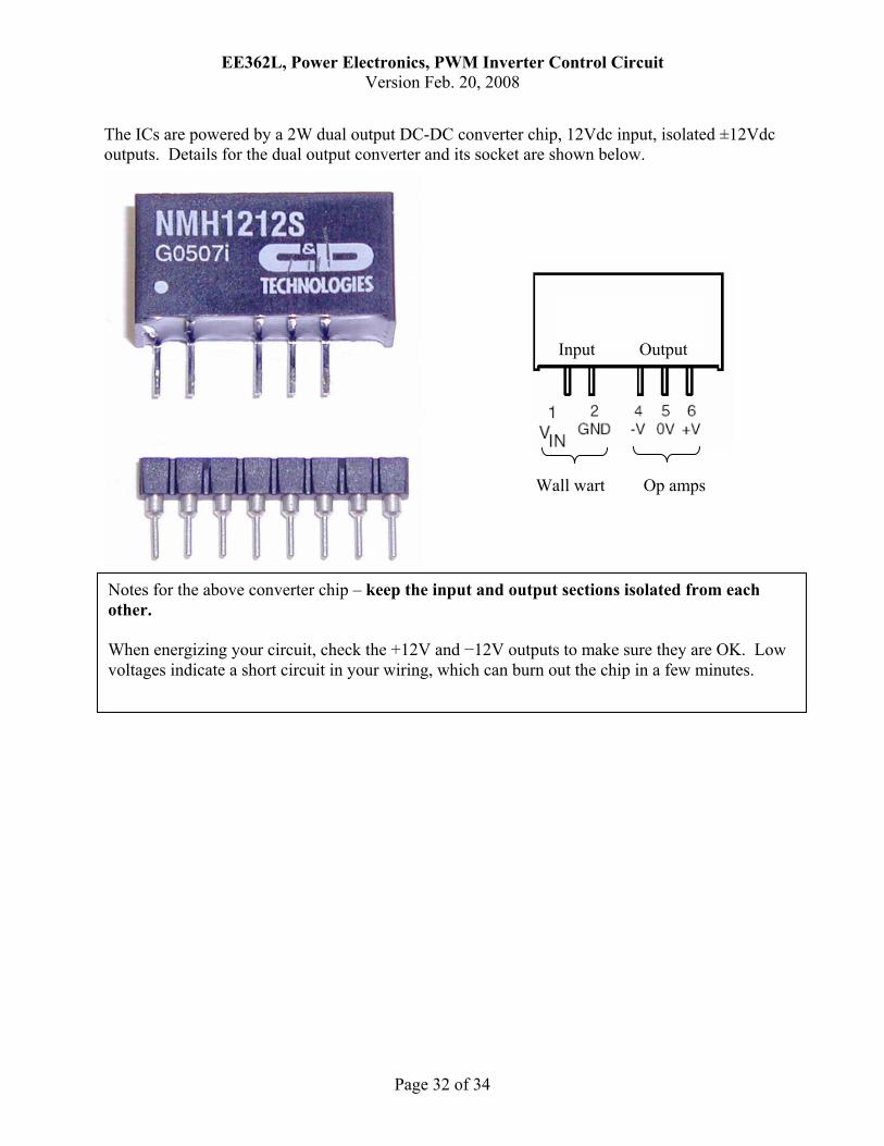
The ICs are powered by a 2W dual output DC-DC converter chip, 12Vdc input, isolated ±12Vdc outputs. Details for the dual output converter and its socket are shown below.
Wall wart Op amps
Notes for the above converter chip – keep the input and output sections isolated from each other. When energizing your circuit, check the +12V and −12V outputs to make sure they are OK. Low voltages indicate a short circuit in your wiring, which can burn out the chip in a few minutes.
Input Output

EE362L, Power Electronics, PWM Inverter Control Circuit Version Feb. 20, 2008
Page 33 of 34
Dual Op Amp
Dual Comparator
DC-DC Converter

EE362L, Power Electronics, PWM Inverter Control Circuit Version Feb. 20, 2008
Page 34 of 34
Triangle wave generator