Embed Size (px)
Citation preview
1Subject to change without noticewwwcreecomrf
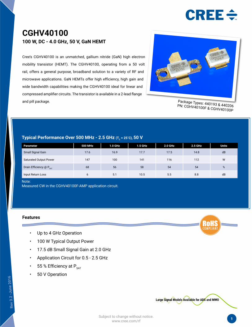
CGHV40100100 W DC - 40 GHz 50 V GaN HEMT
Creersquos CGHV40100 is an unmatched gallium nitride (GaN) high electron
mobility transistor (HEMT) The CGHV40100 operating from a 50 volt
rail offers a general purpose broadband solution to a variety of RF and
microwave applications GaN HEMTs offer high efficiency high gain and
wide bandwidth capabilities making the CGHV40100 ideal for linear and
compressed amplifier circuits The transistor is available in a 2-lead flange
and pill package
Rev
32
-Jun
e 20
16
Package Types 440193 amp 440206PN CGHV40100F amp CGHV40100P
Features
bull Up to 4 GHz Operation
bull 100 W Typical Output Power
bull 175 dB Small Signal Gain at 20 GHz
bull Application Circuit for 05 - 25 GHz
bull 55 Efficiency at PSAT
bull 50 V Operation
Typical Performance Over 500 MHz - 25 GHz (TC = 25˚C) 50 V
Parameter 500 MHz 10 GHz 15 GHz 20 GHz 25 GHz Units
Small Signal Gain 176 169 177 175 148 dB
Saturated Output Power 147 100 141 116 112 W
Drain Efficiency PSAT 68 56 58 54 54
Input Return Loss 6 51 105 55 88 dB
NoteMeasured CW in the CGHV40100F-AMP application circuit
2 CGHV40100 Rev 32
Cree Inc4600 Silicon Drive
Durham North Carolina USA 27703USA Tel +19193135300
Fax +1919869CREEFax +19198692733
wwwcreecomrf
Copyright copy 2014-2016 Cree Inc All rights reserved The information in this document is subject to change without notice Cree and the Cree logo are registered trademarks of Cree Inc
Absolute Maximum Ratings (not simultaneous) at 25˚C Case Temperature
Parameter Symbol Rating Units Conditions
Drain-Source Voltage VDSS 125 Volts 25˚C
Gate-to-Source Voltage VGS -10 +2 Volts 25˚C
Storage Temperature TSTG -65 +150 ˚C
Operating Junction Temperature TJ 225 ˚C
Maximum Forward Gate Current IGMAX 208 mA 25˚C
Maximum Drain Current1 IDMAX 87 A 25˚C
Soldering Temperature2 TS 245 ˚C
Screw Torque τ 40 in-oz
Thermal Resistance Junction to Case3 RθJC 162 ˚CW 85˚C
Thermal Resistance Junction to Case4 RθJC 172 ˚CW 85˚C
Case Operating Temperature5 TC -40 +150 ˚C
Note1 Current limit for long term reliable operation2 Refer to the Application Note on soldering at wwwcreecomRFDocument-Library3 Measured for the CGHV40100P at PDISS = 83 W4 Measured for the CGHV40100F at PDISS = 83 W5 See also Power Derating Curve on Page 5
Electrical Characteristics (TC = 25˚C)
Characteristics Symbol Min Typ Max Units Conditions
DC Characteristics1
Gate Threshold Voltage VGS(th) -38 -30 -23 VDC VDS = 10 V ID = 208 mA
Gate Quiescent Voltage VGS(Q) ndash -27 ndash VDC VDS = 50 V ID = 06 A
Saturated Drain Current2 IDS 156 187 ndash A VDS = 60 V VGS = 20 V
Drain-Source Breakdown Voltage VBR 150 ndash ndash VDC VGS = -8 V ID = 208 mA
RF Characteristics3 (TC = 25˚C F0 = 20 GHz unless otherwise noted)
Small Signal Gain GSS ndash 175 ndash dB VDD = 50 V IDQ = 06 A
Power Gain GP ndash 110 ndash dB VDD = 50 V IDQ = 06 A POUT = PSAT
Power Output at Saturation4 PSAT ndash 116 ndash W VDD = 50 V IDQ = 06 A
Drain Efficiency η ndash 54 ndash VDD = 50 V IDQ = 06 A POUT = PSAT
Output Mismatch Stress VSWR ndash ndash 10 1 YNo damage at all phase angles VDD = 50 V IDQ = 06 A POUT = 100 W CW
Dynamic Characteristics5
Input Capacitance CGS ndash 293 ndash pF VDS = 50 V Vgs = -8 V f = 1 MHz
Output Capacitance CDS ndash 73 ndash pF VDS = 50 V Vgs = -8 V f = 1 MHz
Feedback Capacitance CGD ndash 061 ndash pF VDS = 50 V Vgs = -8 V f = 1 MHz
Notes1 Measured on wafer prior to packaging2 Scaled from PCM data3 Measured in CGHV40100-AMP4 PSAT is defined as IG = 0208 mA5 Includes package
3 CGHV40100 Rev 32
Cree Inc4600 Silicon Drive
Durham North Carolina USA 27703USA Tel +19193135300
Fax +1919869CREEFax +19198692733
wwwcreecomrf
Copyright copy 2014-2016 Cree Inc All rights reserved The information in this document is subject to change without notice Cree and the Cree logo are registered trademarks of Cree Inc
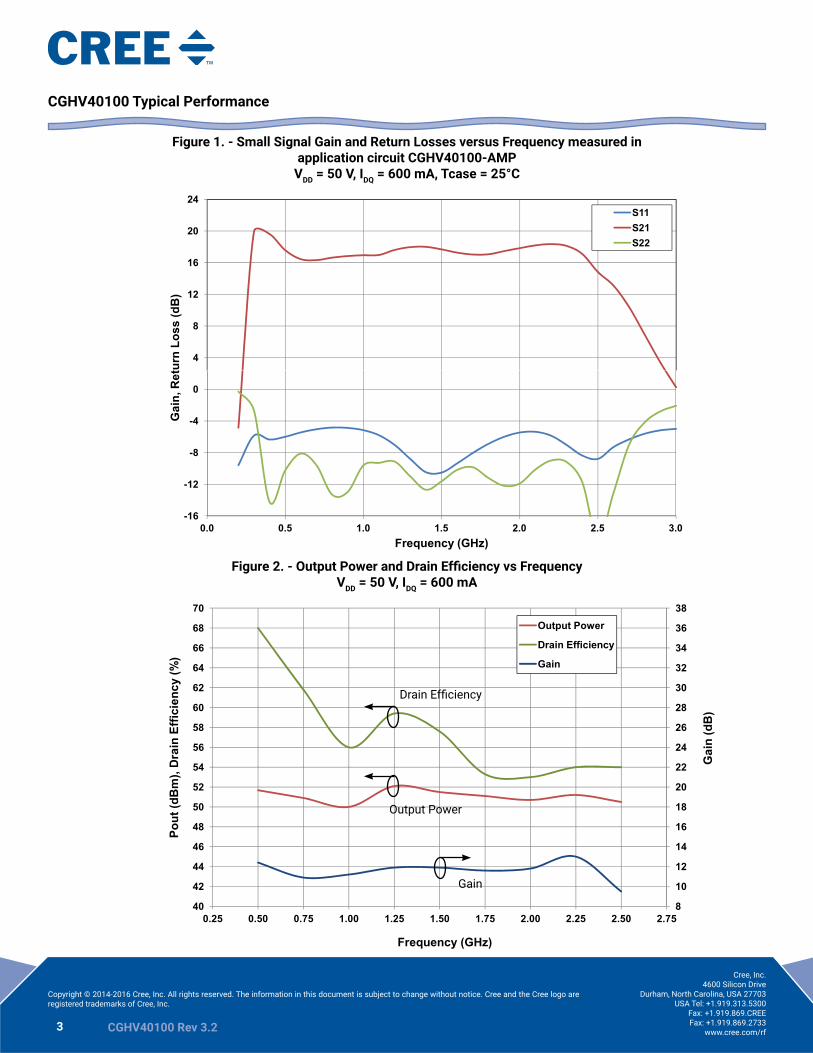
CGHV40100 Typical Performance
Figure 1 - Small Signal Gain and Return Losses versus Frequency measured in application circuit CGHV40100-AMP
VDD = 50 V IDQ = 600 mA Tcase = 25degC
Figure 2 - Output Power and Drain Efficiency vs Frequency VDD = 50 V IDQ = 600 mA
22
24
26
28
30
32
34
36
38
54
56
58
60
62
64
66
68
70
Gai
n(d
B)
Pout
(dB
m)
Dra
inEf
ficie
ncy
()
CGHV40100F in Applications CircuitVdd = 50 V Idq = 600 mA Tcase = 25degC
CW Psat
Output Power
Drain Efficiency
Gain
8
10
12
14
16
18
20
22
40
42
44
46
48
50
52
54
025 050 075 100 125 150 175 200 225 250 275
Pout
(dB
m)
Dra
inEf
ficie
ncy
()
Frequency (GHz)
Drain Efficiency
Output Power
Gain
4
8
12
16
20
24
Gai
nR
etur
nLo
ss(d
B)
Small Signal S-parametersCGHV40100F in Applications Circuit
Vdd = 50 V Idq = 600 mA Tcase = 25degC
S11S21S22
-16
-12
-8
-4
0
00 05 10 15 20 25 30
Gai
nR
etur
nLo
ss(d
B)
Frequency (GHz)
4 CGHV40100 Rev 32
Cree Inc4600 Silicon Drive
Durham North Carolina USA 27703USA Tel +19193135300
Fax +1919869CREEFax +19198692733
wwwcreecomrf
Copyright copy 2014-2016 Cree Inc All rights reserved The information in this document is subject to change without notice Cree and the Cree logo are registered trademarks of Cree Inc
CGHV40100 Typical Performance
Figure 3 - Third Order Intermodulation Distortion vs Average Output Powermeasured in Broadband Amplifier Circuit CGHV40100-AMP
Spacing = 1 MHz VDD = 50 V IDQ = 600 mA Tcase = 25degC
Figure 4 - Third Order Intermodulation Distortion vs Frequencymeasured in Broadband Amplifier Circuit CGHV40100-AMP
Spacing = 1 MHz VDD = 50 V IDQ = 600 mA Tcase = 25degC
-30
-25
-20
-15
-10
-5
0
IMD
3(d
Bc)
CGHV40100F in Applications CircuitVdd = 50 V Idq = 600 mA Tcase = 25degC
1 MHz Two Tone Spacing
05 GHz
15 GHz
25 GHz
-60
-55
-50
-45
-40
-35
-30
27 29 31 33 35 37 39 41 43 45 47Average Output Power (dBm)
-30
-25
-20
-15
-10
-5
0
IMD
3(d
Bc)
CGHV40100F in Applications CircuitVdd = 50 V Idq = 600 mA Tcase = 25degC
1 MHz Two Tone Spacing 10W Average Pout
-60
-55
-50
-45
-40
-35
-30
025 050 075 100 125 150 175 200 225 250 275Frequency (GHz)
5 CGHV40100 Rev 32
Cree Inc4600 Silicon Drive
Durham North Carolina USA 27703USA Tel +19193135300
Fax +1919869CREEFax +19198692733
wwwcreecomrf
Copyright copy 2014-2016 Cree Inc All rights reserved The information in this document is subject to change without notice Cree and the Cree logo are registered trademarks of Cree Inc
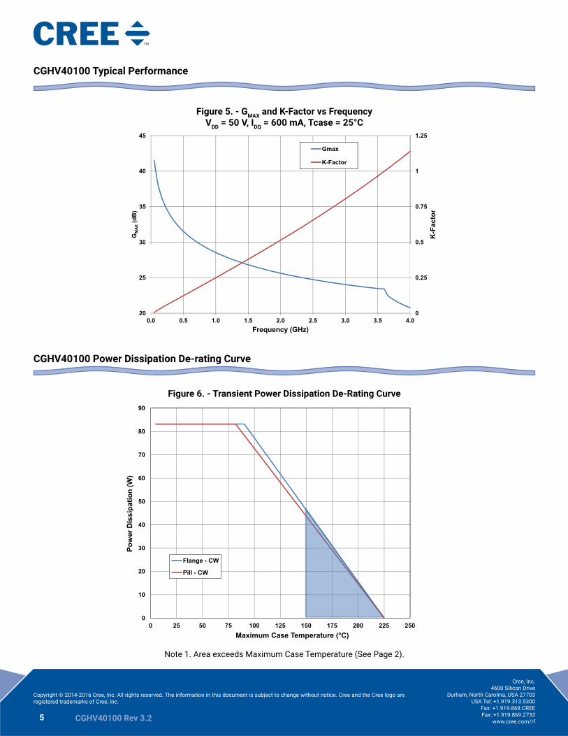
CGHV40100 Typical Performance
Figure 5 - GMAX and K-Factor vs FrequencyVDD = 50 V IDQ = 600 mA Tcase = 25degC
CGHV40100 Power Dissipation De-rating Curve
Figure 6 - Transient Power Dissipation De-Rating Curve
Note 1 Area exceeds Maximum Case Temperature (See Page 2)
05
075
1
125
30
35
40
45
K-F
acto
r
GM
AX(d
B)
Maximum Avaliable Gain amp K-FactorCGHV40100
Vdd = 50 V Idq = 600 mA Tcase = 25degC
Gmax
K-Factor
0
025
05
20
25
30
00 05 10 15 20 25 30 35 40Frequency (GHz)
40
50
60
70
80
90
Pow
erD
issi
patio
n(W
)
CGHV40100 Power Dissipation De-Rating Curve
0
10
20
30
0 25 50 75 100 125 150 175 200 225 250
Pow
erD
issi
patio
n(W
)
Maximum Case Temperature (degC)
Flange - CW
Pill - CW
6 CGHV40100 Rev 32
Cree Inc4600 Silicon Drive
Durham North Carolina USA 27703USA Tel +19193135300
Fax +1919869CREEFax +19198692733
wwwcreecomrf
Copyright copy 2014-2016 Cree Inc All rights reserved The information in this document is subject to change without notice Cree and the Cree logo are registered trademarks of Cree Inc
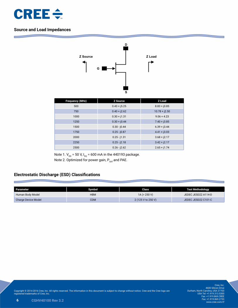
Source and Load Impedances
Frequency (MHz) Z Source Z Load
500 043 + j525 883 + j085
750 040 + j262 1078 + j250
1000 030 + j131 906 + 423
1250 030 + j044 740 + j385
1500 030 - j044 639 + j344
1750 025 - j087 441 + j303
2000 025 - j131 368 + j217
2250 025 - j218 342 + j217
2500 026 - j262 265 + j174
Note 1 VDD = 50 V IDQ = 600 mA in the 440193 packageNote 2 Optimized for power gain PSAT and PAE
Electrostatic Discharge (ESD) Classifications
Parameter Symbol Class Test Methodology
Human Body Model HBM 1A (gt 250 V) JEDEC JESD22 A114-D
Charge Device Model CDM 2 (125 V to 250 V) JEDEC JESD22 C101-C
D
Z Source Z Load
G
S
7 CGHV40100 Rev 32
Cree Inc4600 Silicon Drive
Durham North Carolina USA 27703USA Tel +19193135300
Fax +1919869CREEFax +19198692733
wwwcreecomrf
Copyright copy 2014-2016 Cree Inc All rights reserved The information in this document is subject to change without notice Cree and the Cree logo are registered trademarks of Cree Inc
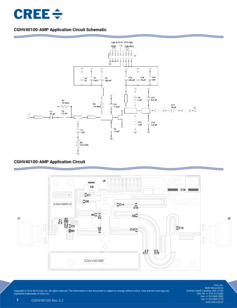
CGHV40100-AMP Application Circuit Schematic
CGHV40100-AMP Application Circuit
8 CGHV40100 Rev 32
Cree Inc4600 Silicon Drive
Durham North Carolina USA 27703USA Tel +19193135300
Fax +1919869CREEFax +19198692733
wwwcreecomrf
Copyright copy 2014-2016 Cree Inc All rights reserved The information in this document is subject to change without notice Cree and the Cree logo are registered trademarks of Cree Inc
CGHV40100-AMP Application Circuit Bill of Materials
Designator Description Qty
C1 C13 C15 CAP 39 pF plusmn 01 pF 250V 0805 ATC600F 3
C2 CAP 75 pF plusmn 01 pF 250 V 0806 ATC600F 1
C3 CAP 3 pF plusmn 01 pF 250 V 0805 ATC600F 1
C4 C5 CAP 15 pF plusmn 01 pF 250 V 0805 ATC600F 2
C7 CAP 33000 pF 0805 100V X7R 1
C6 C14 CAP 240 pF plusmn 05 pF 250 V 0805 ATC600F 2
C8 CAP 10 UF 16V TANTALUM 2312 1
C9 C10 CAP 1 pF plusmn 01 pF 250 V 0805 ATC600F 2
C11 C12 CAP 05 pF plusmn 01 pF 250 V 0805 ATC600F 2
C16 CAP 100 UF 20 160 V ELEC 1
R1 RES 24 OHMS IMS ND3-1005CS24R0G 1
R2 RED 100 OHMS IMS ND3-0805EW1000G 1
R3 RES 39 OHMS 0805 1
J1 J2 CONN SMA PANEL MOUNT JACK 2
J3 HEADER RTgtPLZ 1CEN LK 9POS 1
BASEPLATE CGH35120 1
PCB RO4350B 25rdquo X 4rdquo X 0020rdquo CGHV40100F 1
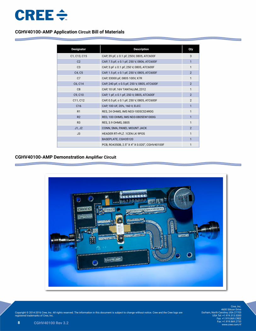
CGHV40100-AMP Demonstration Amplifier Circuit
9 CGHV40100 Rev 32
Cree Inc4600 Silicon Drive
Durham North Carolina USA 27703USA Tel +19193135300
Fax +1919869CREEFax +19198692733
wwwcreecomrf
Copyright copy 2014-2016 Cree Inc All rights reserved The information in this document is subject to change without notice Cree and the Cree logo are registered trademarks of Cree Inc
Product Dimensions CGHV40100F (Package Type mdash 440193)
Product Dimensions CGHV40100P (Package Type mdash 440206)
10 CGHV40100 Rev 32
Cree Inc4600 Silicon Drive
Durham North Carolina USA 27703USA Tel +19193135300
Fax +1919869CREEFax +19198692733
wwwcreecomrf
Copyright copy 2014-2016 Cree Inc All rights reserved The information in this document is subject to change without notice Cree and the Cree logo are registered trademarks of Cree Inc
Part Number System
Parameter Value Units
Upper Frequency1 40 GHz
Power Output 100 W
Package Flange -
Table 1Note1 Alpha characters used in frequency code indicate a value greater than 99 GHz See Table 2 for value
Character Code Code Value
A 0
B 1
C 2
D 3
E 4
F 5
G 6
H 7
J 8
K 9
Examples 1A = 100 GHz2H = 270 GHz
Table 2
PackagePower Output (W)Upper Frequency (GHz)Cree GaN High Voltage
CGHV40100F
11 CGHV40100 Rev 32
Cree Inc4600 Silicon Drive
Durham North Carolina USA 27703USA Tel +19193135300
Fax +1919869CREEFax +19198692733
wwwcreecomrf
Copyright copy 2014-2016 Cree Inc All rights reserved The information in this document is subject to change without notice Cree and the Cree logo are registered trademarks of Cree Inc
Product Ordering Information
Order Number Description Unit of Measure Image
CGHV40100F GaN HEMT Each
CGHV40100P GaN HEMT Each
CGHV40100-TB Test board without GaN HEMT Each
CGHV40100F-AMP Test board with GaN HEMT (flanged) installed Each
CGHV40100P-AMP Test board with GaN HEMT(pill) installed Each Photo TBD
12 CGHV40100 Rev 32
Cree Inc4600 Silicon Drive
Durham North Carolina USA 27703USA Tel +19193135300
Fax +1919869CREEFax +19198692733
wwwcreecomrf
Copyright copy 2014-2016 Cree Inc All rights reserved The information in this document is subject to change without notice Cree and the Cree logo are registered trademarks of Cree Inc
Disclaimer
Specifications are subject to change without notice Cree Inc believes the information contained within this data sheet to be accurate
and reliable However no responsibility is assumed by Cree for any infringement of patents or other rights of third parties which may
result from its use No license is granted by implication or otherwise under any patent or patent rights of Cree Cree makes no warranty
representation or guarantee regarding the suitability of its products for any particular purpose ldquoTypicalrdquo parameters are the average
values expected by Cree in large quantities and are provided for information purposes only These values can and do vary in different
applications and actual performance can vary over time All operating parameters should be validated by customerrsquos technical experts
for each application Cree products are not designed intended or authorized for use as components in applications intended for surgical
implant into the body or to support or sustain life in applications in which the failure of the Cree product could result in personal injury or
death or in applications for planning construction maintenance or direct operation of a nuclear facility
For more information please contact
Cree Inc4600 Silicon DriveDurham North Carolina USA 27703wwwcreecomRF
Sarah MillerMarketingCree RF Components19194075302
Ryan BakerMarketing amp SalesCree RF Components19194077816
Tom DekkerSales DirectorCree RF Components19194075639
Mouser Electronics
Authorized Distributor
Click to View Pricing Inventory Delivery amp Lifecycle Information Cree Inc
CGHV40100F CGHV40100F-TB
2 CGHV40100 Rev 32
Cree Inc4600 Silicon Drive
Durham North Carolina USA 27703USA Tel +19193135300
Fax +1919869CREEFax +19198692733
wwwcreecomrf
Copyright copy 2014-2016 Cree Inc All rights reserved The information in this document is subject to change without notice Cree and the Cree logo are registered trademarks of Cree Inc
Absolute Maximum Ratings (not simultaneous) at 25˚C Case Temperature
Parameter Symbol Rating Units Conditions
Drain-Source Voltage VDSS 125 Volts 25˚C
Gate-to-Source Voltage VGS -10 +2 Volts 25˚C
Storage Temperature TSTG -65 +150 ˚C
Operating Junction Temperature TJ 225 ˚C
Maximum Forward Gate Current IGMAX 208 mA 25˚C
Maximum Drain Current1 IDMAX 87 A 25˚C
Soldering Temperature2 TS 245 ˚C
Screw Torque τ 40 in-oz
Thermal Resistance Junction to Case3 RθJC 162 ˚CW 85˚C
Thermal Resistance Junction to Case4 RθJC 172 ˚CW 85˚C
Case Operating Temperature5 TC -40 +150 ˚C
Note1 Current limit for long term reliable operation2 Refer to the Application Note on soldering at wwwcreecomRFDocument-Library3 Measured for the CGHV40100P at PDISS = 83 W4 Measured for the CGHV40100F at PDISS = 83 W5 See also Power Derating Curve on Page 5
Electrical Characteristics (TC = 25˚C)
Characteristics Symbol Min Typ Max Units Conditions
DC Characteristics1
Gate Threshold Voltage VGS(th) -38 -30 -23 VDC VDS = 10 V ID = 208 mA
Gate Quiescent Voltage VGS(Q) ndash -27 ndash VDC VDS = 50 V ID = 06 A
Saturated Drain Current2 IDS 156 187 ndash A VDS = 60 V VGS = 20 V
Drain-Source Breakdown Voltage VBR 150 ndash ndash VDC VGS = -8 V ID = 208 mA
RF Characteristics3 (TC = 25˚C F0 = 20 GHz unless otherwise noted)
Small Signal Gain GSS ndash 175 ndash dB VDD = 50 V IDQ = 06 A
Power Gain GP ndash 110 ndash dB VDD = 50 V IDQ = 06 A POUT = PSAT
Power Output at Saturation4 PSAT ndash 116 ndash W VDD = 50 V IDQ = 06 A
Drain Efficiency η ndash 54 ndash VDD = 50 V IDQ = 06 A POUT = PSAT
Output Mismatch Stress VSWR ndash ndash 10 1 YNo damage at all phase angles VDD = 50 V IDQ = 06 A POUT = 100 W CW
Dynamic Characteristics5
Input Capacitance CGS ndash 293 ndash pF VDS = 50 V Vgs = -8 V f = 1 MHz
Output Capacitance CDS ndash 73 ndash pF VDS = 50 V Vgs = -8 V f = 1 MHz
Feedback Capacitance CGD ndash 061 ndash pF VDS = 50 V Vgs = -8 V f = 1 MHz
Notes1 Measured on wafer prior to packaging2 Scaled from PCM data3 Measured in CGHV40100-AMP4 PSAT is defined as IG = 0208 mA5 Includes package
3 CGHV40100 Rev 32
Cree Inc4600 Silicon Drive
Durham North Carolina USA 27703USA Tel +19193135300
Fax +1919869CREEFax +19198692733
wwwcreecomrf
Copyright copy 2014-2016 Cree Inc All rights reserved The information in this document is subject to change without notice Cree and the Cree logo are registered trademarks of Cree Inc
CGHV40100 Typical Performance
Figure 1 - Small Signal Gain and Return Losses versus Frequency measured in application circuit CGHV40100-AMP
VDD = 50 V IDQ = 600 mA Tcase = 25degC
Figure 2 - Output Power and Drain Efficiency vs Frequency VDD = 50 V IDQ = 600 mA
22
24
26
28
30
32
34
36
38
54
56
58
60
62
64
66
68
70
Gai
n(d
B)
Pout
(dB
m)
Dra
inEf
ficie
ncy
()
CGHV40100F in Applications CircuitVdd = 50 V Idq = 600 mA Tcase = 25degC
CW Psat
Output Power
Drain Efficiency
Gain
8
10
12
14
16
18
20
22
40
42
44
46
48
50
52
54
025 050 075 100 125 150 175 200 225 250 275
Pout
(dB
m)
Dra
inEf
ficie
ncy
()
Frequency (GHz)
Drain Efficiency
Output Power
Gain
4
8
12
16
20
24
Gai
nR
etur
nLo
ss(d
B)
Small Signal S-parametersCGHV40100F in Applications Circuit
Vdd = 50 V Idq = 600 mA Tcase = 25degC
S11S21S22
-16
-12
-8
-4
0
00 05 10 15 20 25 30
Gai
nR
etur
nLo
ss(d
B)
Frequency (GHz)
4 CGHV40100 Rev 32
Cree Inc4600 Silicon Drive
Durham North Carolina USA 27703USA Tel +19193135300
Fax +1919869CREEFax +19198692733
wwwcreecomrf
Copyright copy 2014-2016 Cree Inc All rights reserved The information in this document is subject to change without notice Cree and the Cree logo are registered trademarks of Cree Inc
CGHV40100 Typical Performance
Figure 3 - Third Order Intermodulation Distortion vs Average Output Powermeasured in Broadband Amplifier Circuit CGHV40100-AMP
Spacing = 1 MHz VDD = 50 V IDQ = 600 mA Tcase = 25degC
Figure 4 - Third Order Intermodulation Distortion vs Frequencymeasured in Broadband Amplifier Circuit CGHV40100-AMP
Spacing = 1 MHz VDD = 50 V IDQ = 600 mA Tcase = 25degC
-30
-25
-20
-15
-10
-5
0
IMD
3(d
Bc)
CGHV40100F in Applications CircuitVdd = 50 V Idq = 600 mA Tcase = 25degC
1 MHz Two Tone Spacing
05 GHz
15 GHz
25 GHz
-60
-55
-50
-45
-40
-35
-30
27 29 31 33 35 37 39 41 43 45 47Average Output Power (dBm)
-30
-25
-20
-15
-10
-5
0
IMD
3(d
Bc)
CGHV40100F in Applications CircuitVdd = 50 V Idq = 600 mA Tcase = 25degC
1 MHz Two Tone Spacing 10W Average Pout
-60
-55
-50
-45
-40
-35
-30
025 050 075 100 125 150 175 200 225 250 275Frequency (GHz)
5 CGHV40100 Rev 32
Cree Inc4600 Silicon Drive
Durham North Carolina USA 27703USA Tel +19193135300
Fax +1919869CREEFax +19198692733
wwwcreecomrf
Copyright copy 2014-2016 Cree Inc All rights reserved The information in this document is subject to change without notice Cree and the Cree logo are registered trademarks of Cree Inc
CGHV40100 Typical Performance
Figure 5 - GMAX and K-Factor vs FrequencyVDD = 50 V IDQ = 600 mA Tcase = 25degC
CGHV40100 Power Dissipation De-rating Curve
Figure 6 - Transient Power Dissipation De-Rating Curve
Note 1 Area exceeds Maximum Case Temperature (See Page 2)
05
075
1
125
30
35
40
45
K-F
acto
r
GM
AX(d
B)
Maximum Avaliable Gain amp K-FactorCGHV40100
Vdd = 50 V Idq = 600 mA Tcase = 25degC
Gmax
K-Factor
0
025
05
20
25
30
00 05 10 15 20 25 30 35 40Frequency (GHz)
40
50
60
70
80
90
Pow
erD
issi
patio
n(W
)
CGHV40100 Power Dissipation De-Rating Curve
0
10
20
30
0 25 50 75 100 125 150 175 200 225 250
Pow
erD
issi
patio
n(W
)
Maximum Case Temperature (degC)
Flange - CW
Pill - CW
6 CGHV40100 Rev 32
Cree Inc4600 Silicon Drive
Durham North Carolina USA 27703USA Tel +19193135300
Fax +1919869CREEFax +19198692733
wwwcreecomrf
Copyright copy 2014-2016 Cree Inc All rights reserved The information in this document is subject to change without notice Cree and the Cree logo are registered trademarks of Cree Inc
Source and Load Impedances
Frequency (MHz) Z Source Z Load
500 043 + j525 883 + j085
750 040 + j262 1078 + j250
1000 030 + j131 906 + 423
1250 030 + j044 740 + j385
1500 030 - j044 639 + j344
1750 025 - j087 441 + j303
2000 025 - j131 368 + j217
2250 025 - j218 342 + j217
2500 026 - j262 265 + j174
Note 1 VDD = 50 V IDQ = 600 mA in the 440193 packageNote 2 Optimized for power gain PSAT and PAE
Electrostatic Discharge (ESD) Classifications
Parameter Symbol Class Test Methodology
Human Body Model HBM 1A (gt 250 V) JEDEC JESD22 A114-D
Charge Device Model CDM 2 (125 V to 250 V) JEDEC JESD22 C101-C
D
Z Source Z Load
G
S
7 CGHV40100 Rev 32
Cree Inc4600 Silicon Drive
Durham North Carolina USA 27703USA Tel +19193135300
Fax +1919869CREEFax +19198692733
wwwcreecomrf
Copyright copy 2014-2016 Cree Inc All rights reserved The information in this document is subject to change without notice Cree and the Cree logo are registered trademarks of Cree Inc
CGHV40100-AMP Application Circuit Schematic
CGHV40100-AMP Application Circuit
8 CGHV40100 Rev 32
Cree Inc4600 Silicon Drive
Durham North Carolina USA 27703USA Tel +19193135300
Fax +1919869CREEFax +19198692733
wwwcreecomrf
Copyright copy 2014-2016 Cree Inc All rights reserved The information in this document is subject to change without notice Cree and the Cree logo are registered trademarks of Cree Inc
CGHV40100-AMP Application Circuit Bill of Materials
Designator Description Qty
C1 C13 C15 CAP 39 pF plusmn 01 pF 250V 0805 ATC600F 3
C2 CAP 75 pF plusmn 01 pF 250 V 0806 ATC600F 1
C3 CAP 3 pF plusmn 01 pF 250 V 0805 ATC600F 1
C4 C5 CAP 15 pF plusmn 01 pF 250 V 0805 ATC600F 2
C7 CAP 33000 pF 0805 100V X7R 1
C6 C14 CAP 240 pF plusmn 05 pF 250 V 0805 ATC600F 2
C8 CAP 10 UF 16V TANTALUM 2312 1
C9 C10 CAP 1 pF plusmn 01 pF 250 V 0805 ATC600F 2
C11 C12 CAP 05 pF plusmn 01 pF 250 V 0805 ATC600F 2
C16 CAP 100 UF 20 160 V ELEC 1
R1 RES 24 OHMS IMS ND3-1005CS24R0G 1
R2 RED 100 OHMS IMS ND3-0805EW1000G 1
R3 RES 39 OHMS 0805 1
J1 J2 CONN SMA PANEL MOUNT JACK 2
J3 HEADER RTgtPLZ 1CEN LK 9POS 1
BASEPLATE CGH35120 1
PCB RO4350B 25rdquo X 4rdquo X 0020rdquo CGHV40100F 1
CGHV40100-AMP Demonstration Amplifier Circuit
9 CGHV40100 Rev 32
Cree Inc4600 Silicon Drive
Durham North Carolina USA 27703USA Tel +19193135300
Fax +1919869CREEFax +19198692733
wwwcreecomrf
Copyright copy 2014-2016 Cree Inc All rights reserved The information in this document is subject to change without notice Cree and the Cree logo are registered trademarks of Cree Inc
Product Dimensions CGHV40100F (Package Type mdash 440193)
Product Dimensions CGHV40100P (Package Type mdash 440206)
10 CGHV40100 Rev 32
Cree Inc4600 Silicon Drive
Durham North Carolina USA 27703USA Tel +19193135300
Fax +1919869CREEFax +19198692733
wwwcreecomrf
Copyright copy 2014-2016 Cree Inc All rights reserved The information in this document is subject to change without notice Cree and the Cree logo are registered trademarks of Cree Inc
Part Number System
Parameter Value Units
Upper Frequency1 40 GHz
Power Output 100 W
Package Flange -
Table 1Note1 Alpha characters used in frequency code indicate a value greater than 99 GHz See Table 2 for value
Character Code Code Value
A 0
B 1
C 2
D 3
E 4
F 5
G 6
H 7
J 8
K 9
Examples 1A = 100 GHz2H = 270 GHz
Table 2
PackagePower Output (W)Upper Frequency (GHz)Cree GaN High Voltage
CGHV40100F
11 CGHV40100 Rev 32
Cree Inc4600 Silicon Drive
Durham North Carolina USA 27703USA Tel +19193135300
Fax +1919869CREEFax +19198692733
wwwcreecomrf
Copyright copy 2014-2016 Cree Inc All rights reserved The information in this document is subject to change without notice Cree and the Cree logo are registered trademarks of Cree Inc
Product Ordering Information
Order Number Description Unit of Measure Image
CGHV40100F GaN HEMT Each
CGHV40100P GaN HEMT Each
CGHV40100-TB Test board without GaN HEMT Each
CGHV40100F-AMP Test board with GaN HEMT (flanged) installed Each
CGHV40100P-AMP Test board with GaN HEMT(pill) installed Each Photo TBD
12 CGHV40100 Rev 32
Cree Inc4600 Silicon Drive
Durham North Carolina USA 27703USA Tel +19193135300
Fax +1919869CREEFax +19198692733
wwwcreecomrf
Copyright copy 2014-2016 Cree Inc All rights reserved The information in this document is subject to change without notice Cree and the Cree logo are registered trademarks of Cree Inc
Disclaimer
Specifications are subject to change without notice Cree Inc believes the information contained within this data sheet to be accurate
and reliable However no responsibility is assumed by Cree for any infringement of patents or other rights of third parties which may
result from its use No license is granted by implication or otherwise under any patent or patent rights of Cree Cree makes no warranty
representation or guarantee regarding the suitability of its products for any particular purpose ldquoTypicalrdquo parameters are the average
values expected by Cree in large quantities and are provided for information purposes only These values can and do vary in different
applications and actual performance can vary over time All operating parameters should be validated by customerrsquos technical experts
for each application Cree products are not designed intended or authorized for use as components in applications intended for surgical
implant into the body or to support or sustain life in applications in which the failure of the Cree product could result in personal injury or
death or in applications for planning construction maintenance or direct operation of a nuclear facility
For more information please contact
Cree Inc4600 Silicon DriveDurham North Carolina USA 27703wwwcreecomRF
Sarah MillerMarketingCree RF Components19194075302
Ryan BakerMarketing amp SalesCree RF Components19194077816
Tom DekkerSales DirectorCree RF Components19194075639
Mouser Electronics
Authorized Distributor
Click to View Pricing Inventory Delivery amp Lifecycle Information Cree Inc
CGHV40100F CGHV40100F-TB
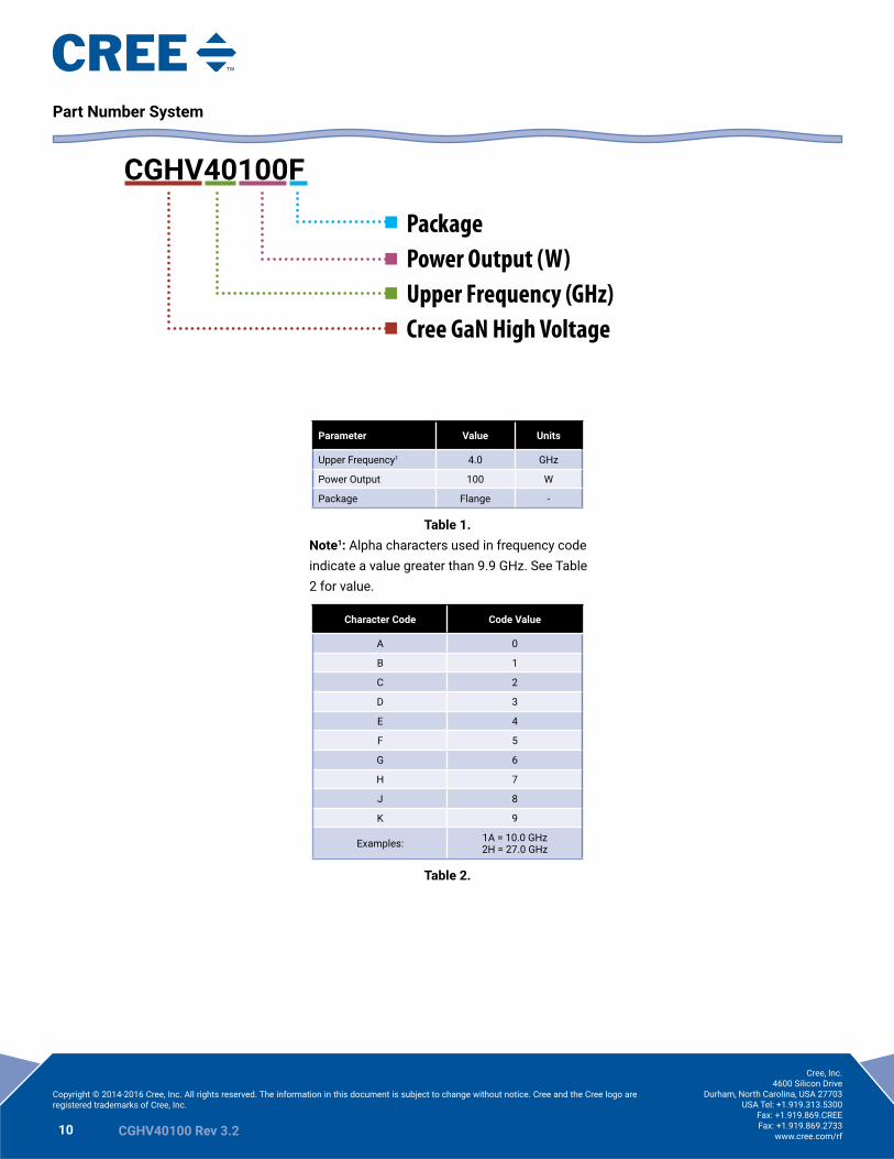
Mouser Electronics
Authorized Distributor
Click to View Pricing Inventory Delivery amp Lifecycle Information Cree Inc
CGHV40100F CGHV40100F-TB


![Cree, CGHV1J070D 70W, DC-18 GHz GaN HEMT DIE (Cree) · vikmwxivihxvehiqevowsj'vii -rg 3xlivxvehiqevow tvshygxerhgsqter] ... 2.00 ghz 0.957 -175.28 2.72 58.56 0.009 -29.21 0.725 -164.11](https://img.pdfslide.net/doc/110x75/5b5ac8947f8b9a302a8c8d43/cree-cghv1j070d-70w-dc-18-ghz-gan-hemt-die-cree-vikmwxivihxvehiqevowsjvii.jpg)