Embed Size (px)
Citation preview

12-/14-Bit High Bandwidth Multiplying DACs with Serial Interface
Data Sheet AD5444/AD5446
Rev. F Document Feedback Information furnished by Analog Devices is believed to be accurate and reliable. However, no responsibility is assumed by Analog Devices for its use, nor for any infringements of patents or other rights of third parties that may result from its use. Specifications subject to change without notice. No license is granted by implication or otherwise under any patent or patent rights of Analog Devices. Trademarks and registered trademarks are the property of their respective owners.
One Technology Way, P.O. Box 9106, Norwood, MA 02062-9106, U.S.A. Tel: 781.329.4700 ©2004–2016 Analog Devices, Inc. All rights reserved. Technical Support www.analog.com
FEATURES 12 MHz multiplying bandwidth INL of ±0.5 LSB at 12 bits Pin-compatible 12-/14-bit current output DAC 2.5 V to 5.5 V supply operation 10-lead MSOP package ±10 V reference input 50 MHz serial interface 2.7 MSPS update rate Extended temperature range: −40°C to +125°C 4-quadrant multiplication Power-on reset with brownout detection 0.4 µA typical current consumption Guaranteed monotonic
APPLICATIONS Portable, battery-powered applications Waveform generators Analog processing Instrumentation applications Programmable amplifiers and attenuators Digitally controlled calibration Programmable filters and oscillators Composite video Ultrasound Gain, offset, and voltage trimming
FUNCTIONAL BLOCK DIAGRAM
0458
8-00
1
POWER-ONRESET
GND
VREF
RFB
IOUT1
IOUT2
R
SDOCONTROL LOGIC ANDINPUT SHIFT REGISTER
DAC REGISTER
12-BITR-2R DAC
INPUT LATCH
SCLKSDIN
SYNC
VDD
AD5444/AD5446
Figure 1.
GENERAL DESCRIPTION The AD5444/AD54461 are CMOS 12-bit and 14-bit, current output, digital-to-analog converters (DACs). Operating from a single 2.5 V to 5.5 V power supply, these devices are suited for battery-powered and other applications.
As a result of the CMOS submicron manufacturing process, these parts offer excellent 4-quadrant multiplication char-acteristics of up to 12 MHz.
These DACs use a double-buffered, 3-wire serial interface that is compatible with SPI®, QSPI™, MICROWIRE™, and most DSP interface standards. On power-up, the internal shift register and latches are filled with 0s, and the DAC output is at zero scale.
The applied external reference input voltage (VREF) determines the full-scale output current. These parts can handle ±10 V inputs on the reference, despite operating from a single-supply power supply of 2.5 V to 5.5 V. An integrated feedback resistor (RFB) provides temperature tracking and full-scale voltage output when combined with an external current-to-voltage precision amplifier. The AD5444/AD5446 DACs are available in small 10-lead MSOP packages, which are pin-compatible with the AD5425/AD5426/AD5432/AD5443 family of DACs.
The EV-AD5443/46/53SDZ board is available for evaluating DAC performance. For more information, see the UG-327 evaluation board user guide.
1 US Patent Number 5,689,257.

AD5444/AD5446 Data Sheet
Rev. F | Page 2 of 28
TABLE OF CONTENTS Features .............................................................................................. 1 Applications ....................................................................................... 1 General Description ......................................................................... 1 Functional Block Diagram .............................................................. 1 Revision History ............................................................................... 2 Specifications ..................................................................................... 3
Timing Characteristics ................................................................ 5 Absolute Maximum Ratings ............................................................ 6
ESD Caution .................................................................................. 6 Pin Configuration and Function Descriptions ............................. 7 Typical Performance Characteristics ............................................. 8 Terminology .................................................................................... 14 General Description ....................................................................... 15
DAC Section................................................................................ 15 Circuit Operation ....................................................................... 15 Single-Supply Applications ....................................................... 17 Adding Gain ................................................................................ 17 Divider or Programmable Gain Element ................................ 17 Amplifier Selection .................................................................... 18 Reference Selection .................................................................... 18
Serial Interface ................................................................................ 20 Microprocessor Interfacing ....................................................... 21
PCB Layout and Power Supply Decoupling ................................ 23 Overview of Current Output Devices .......................................... 24 Outline Dimensions ....................................................................... 25
Ordering Guide .......................................................................... 25
REVISION HISTORY 2/16—Rev. E to Rev. F Changes to Applications Section .................................................... 1 Deleted Positive Output Voltage Section and Figure 41; Renumbered Sequentially .............................................................. 17 Changes to Adding Gain Section ................................................. 17 Changes to ADSP-2191M to AD5444/AD5446 Interface Section, Blackfin to AD5444/AD5446 Interface Section, Figure 46, Figure 47, and Figure 48 .............................................. 21 Changes to Overview of Current Output Devices Section Heading ............................................................................................ 24 Changes to Ordering Guide .......................................................... 25 6/13—Rev. D to Rev. E Changes to General Description Section ...................................... 1 Change to Figure 46 and Figure 47 .............................................. 21 Changes to Ordering Guide .......................................................... 25 4/12—Rev. C to Rev. D Changes to General Description Section ...................................... 1 Deleted Evaluation Board for the DAC Section ......................... 23 Deleted Power Supplies for the Evaluation Board Section ....... 23 Deleted Figure 54; Renumbered Sequentially............................. 24 Deleted Figure 55 and Figure 56 ................................................... 25 Updated Outline Dimensions ....................................................... 25 Changes to Ordering Guide .......................................................... 25 Deleted Figure 57 ............................................................................ 26 4/07—Rev. B to Rev. C Changes to Table 9 .......................................................................... 19
Changes to Ordering Guide .......................................................... 28 Changes to Features .......................................................................... 1 Changes to General Description ..................................................... 1 Changes to Table 1 ............................................................................. 3 Changes to Figure 22 ...................................................................... 10 Changes to Figure 23 ...................................................................... 10 Changes to Table 9 .......................................................................... 19 Changes to Table 12 ....................................................................... 27 Updated Outline Dimensions ....................................................... 28 Changes to Ordering Guide .......................................................... 28 4/05—Rev. 0 to Rev. A Added AD5446 ................................................................... Universal Changes to Features .......................................................................... 1 Changes to General Description ..................................................... 1 Changes to Specifications ................................................................. 3 Inserted Figure 7; Renumbered Sequentially................................. 9 Inserted Figure 9; Renumbered Sequentially................................. 9 Inserted Figure 13; Renumbered Sequentially ........................... 10 Changes to Figure 22 ...................................................................... 11 Changes to Figure 23 ...................................................................... 11 Changes to Serial Interface ............................................................ 20 Changes to Figure 44 ...................................................................... 20 Changes to Figure 45 ...................................................................... 20 Updated Outline Dimensions ....................................................... 28 Changes to Ordering Guide .......................................................... 28 10/04—Revision 0: Initial Version

Data Sheet AD5444/AD5446
Rev. F | Page 3 of 28
SPECIFICATIONS VDD = 2.5 V to 5.5 V, VREF = 10 V, IOUT2 = 0 V. Temperature range for Y version: −40°C to +125°C. All specifications TMIN to TMAX, unless otherwise noted. DC performance measured with OP177, and ac performance measured with AD8038, unless otherwise noted.
Table 1. Parameter Min Typ Max Unit Conditions STATIC PERFORMANCE
AD5444 Resolution 12 Bits Relative Accuracy ±0.5 LSB Differential Nonlinearity ±1 LSB Guaranteed monotonic Total Unadjusted Error (TUE) ±1 LSB Gain Error ±0.5 LSB
AD5446 Resolution 14 Bits Relative Accuracy ±2 LSB Differential Nonlinearity −1/+2 LSB Guaranteed monotonic Total Unadjusted Error (TUE) ±4 LSB Gain Error ±2.5 LSB
Gain Error Temperature Coefficient1 ±2 ppm FSR/°C Output Leakage Current ±1 nA Data = 0x0000, TA = 25°C, IOUT1
±10 nA Data = 0x0000, TA = −40°C to +125°C, IOUT1 REFERENCE INPUT1
Reference Input Range ±10 V VREF Input Resistance 7 9 11 kΩ Input resistance TC = −50 ppm/°C RFB Feedback Resistance 7 9 11 kΩ Input resistance TC = −50 ppm/°C Input Capacitance
Zero-Scale Code 18 22 pF Full-Scale Code 18 22 pF
DIGITAL INPUTS/OUTPUTS1 Input High Voltage, VIH 2.0 V VDD = 3.6 V to 5 V 1.7 V VDD = 2.5 V to 3.6 V Input Low Voltage, VIL 0.8 V VDD = 2.7 V to 5.5 V 0.7 V VDD = 2.5 V to 2.7 V Output High Voltage, VOH VDD − 1 V VDD = 4.5 V to 5 V, ISOURCE = 200 µA VDD − 0.5 V VDD = 2.5 V to 3.6 V, ISOURCE = 200 µA Output Low Voltage, VOL 0.4 V VDD = 4.5 V to 5 V, ISINK = 200 µA 0.4 V VDD = 2.5 V to 3.6 V, ISINK = 200 µA Input Leakage Current, IIL ±1 nA TA = 25°C ±10 nA TA = −40°C to +125°C Input Capacitance 10 pF

AD5444/AD5446 Data Sheet
Rev. F | Page 4 of 28
Parameter Min Typ Max Unit Conditions DYNAMIC PERFORMANCE1
Reference Multiplying Bandwidth 12 MHz VREF = ±3.5 V, DAC loaded with all 1s Multiplying Feedthrough Error VREF = ±3.5 V, DAC loaded with all 0s 72 dB 100 kHz 64 dB 1 MHz 44 dB 10 MHz Output Voltage Settling Time VREF = 10 V, RLOAD = 100 Ω, DAC latch alternately
loaded with 0s and 1s Measured to ±1 mV of FS 100 110 ns Measured to ±4 mV of FS 24 40 ns Measured to ±16 mV of FS 16 33 ns
Digital Delay 20 40 ns Interface delay time 10%-to-90% Settling Time 10 30 ns Rise and fall time, VREF = 10 V, RLOAD = 100 Ω Digital-to-Analog Glitch Impulse 2 nV-s 1 LSB change around major carry, VREF = 0 V Output Capacitance
IOUT1 13 pF DAC latches loaded with all 0s 28 pF DAC latches loaded with all 1s IOUT2 18 pF DAC latches loaded with all 0s
5 pF DAC latches loaded with all 1s Digital Feedthrough 0.5 nV-s Feedthrough to DAC output with CS high and
alternate loading of all 0s and all 1s Analog THD 83 dB VREF = 3.5 V p-p, all 1s loaded, f = 1 kHz Digital THD Clock = 1 MHz, VREF = 3.5 V
50 kHz fOUT 71 dB 20 kHz fOUT 77 dB Output Noise Spectral Density 25 nV/√Hz @ 1 kHz SFDR Performance (Wide Band) Clock = 10 MHz, VREF = 3.5 V
50 kHz fOUT 78 dB 20 kHz fOUT 74 dB
SFDR Performance (Narrow Band) Clock = 1 MHz, VREF = 3.5 V 50 kHz fOUT 87 dB 20 kHz fOUT 85 dB
Intermodulation Distortion 79 dB f1 = 20 kHz, f2 = 25 kHz, clock = 1 MHz, VREF = 3.5 V POWER REQUIREMENTS
Power Supply Range, VDD 2.5 5.5 V Supply Current, IDD 0.4 10 µA TA = −40°C to +125°C, logic inputs = 0 V or VDD 0.6 µA TA = 25°C, logic inputs = 0 V or VDD Power Supply Sensitivity1 0.001 %/% ∆VDD = ±5%
1 Guaranteed by design and characterization; not subject to production test.

Data Sheet AD5444/AD5446
Rev. F | Page 5 of 28
TIMING CHARACTERISTICS All input signals are specified with tr = tf = 1 ns (10% to 90% of VDD) and timed from a voltage level of (VIL + VIH)/2. VDD = 2.5 V to 5.5 V, VREF = 10 V, IOUT2 = 0 V, temperature range for Y version: −40°C to +125°C; all specifications TMIN to TMAX, unless otherwise noted.
Table 2.
Parameter1 VDD = 4.5 V to 5.5 V
VDD = 2.5 V to 5.5 V Unit Conditions/Comments
fSCLK 50 50 MHz max Maximum clock frequency. t1 20 20 ns min SCLK cycle time. t2 8 8 ns min SCLK high time. t3 8 8 ns min SCLK low time. t4 8 8 ns min SYNC falling edge to SCLK active edge setup time.
t5 5 5 ns min Data setup time. t6 4.5 4.5 ns min Data hold time. t7 5 5 ns min SYNC rising edge to SCLK active edge setup time
t8 30 30 ns min Minimum SYNC high time.
t9 23 30 ns min SCLK active edge to SDO valid. Update Rate 2.7 2.7 MSPS Consists of cycle time, SYNC high time, data setup time and output
voltage settling time. 1 Guaranteed by design and characterization; not subject to production test.
0458
8-00
2
t7
t1
t3t2
t4
t5
t6
DB15 DB0
SCLK
SYNC
SDIN
t8
Figure 2. Standalone Timing Diagram
DB15 (N) DB0 (N) DB15(N + 1)
DB0(N + 1)
SCLK
SDIN
SDO
NOTESALTERNATIVELY, DATA CAN BE CLOCKED INTO INPUT SHIFT REGISTER ON RISING EDGE OF SCLK ASDETERMINED BY CONTROL BITS. IN THIS CASE, DATA IS CLOCKED OUT OF SDO ON FALLINGEDGE OF SCLK. TIMING AS ABOVE, WITH SCLK INVERTED.
t4
t5
t6
t2
t1
t3 t7t8
t9
DB15 (N) DB0 (N)
SYNC
0458
8-00
3
Figure 3. Daisy-Chain Timing Diagram

AD5444/AD5446 Data Sheet
Rev. F | Page 6 of 28
ABSOLUTE MAXIMUM RATINGS TA = 25°C, unless otherwise noted. Transient currents of up to 100 mA do not cause SCR latch-up.
Table 3. Parameter Rating VDD to GND −0.3 V to +7 V VREF, RFB to GND −12 V to +12 V IOUT1, IOUT2 to GND −0.3 V to +7 V Logic Inputs and Outputs1 −0.3 V to VDD + 0.3 V Input Current (All Pins Except Supplies) ±10 mA Operating Temperature Range −40°C to +125°C Extended (Y Version) Storage Temperature Range −65°C to +150°C Junction Temperature 150°C 10-lead MSOP θJA Thermal Impedance 206°C/W Lead Temperature, Soldering (10 sec) 300°C IR Reflow, Peak Temperature (<20 sec) 235°C 1 Overvoltages at SCLK, SYNC, and SDIN are clamped by internal diodes.
Stresses at or above those listed under Absolute Maximum Ratings may cause permanent damage to the product. This is a stress rating only; functional operation of the product at these or any other conditions above those indicated in the operational section of this specification is not implied. Operation beyond the maximum operating conditions for extended periods may affect product reliability.
Only one absolute maximum rating can be applied at any one time.
IOL200µA
TOOUTPUT
PIN
200µA IOH
CL20pF
VOH (MIN) +VOL (MAX)2
0458
8-00
4
Figure 4. Load Circuit for SDO Timing Specifications
ESD CAUTION

Data Sheet AD5444/AD5446
Rev. F | Page 7 of 28
PIN CONFIGURATION AND FUNCTION DESCRIPTIONS
0458
8-00
5
10
9
8
7
6
1
2
3
4
5
IOUT1
IOUT2
GND
SCLK
SDIN
RFB
VREF
VDD
SDO
AD5444/AD5446TOP VIEW
(Not to Scale)
SYNC
Figure 5. Pin Configuration
Table 4. Pin Function Descriptions Pin No. Mnemonic Description 1 IOUT1 DAC Current Output. 2 IOUT2 DAC Analog Ground. This pin should normally be tied to the analog ground of the system. 3 GND Ground Pin. 4 SCLK Serial Clock Input. By default, data is clocked into the input shift register on the falling edge of the serial clock
input. Alternatively, by means of the serial control bits, the device can be configured such that data is clocked into the shift register on the rising edge of SCLK.
5 SDIN Serial Data Input. Data is clocked into the 16-bit input register on the active edge of the serial clock input. By default on power-up, data is clocked into the shift register on the falling edge of SCLK. The control bits allow the user to change the active edge to the rising edge.
6 SYNC Active Low Control Input. This is the frame synchronization signal for the input data. When SYNC is taken low, data is loaded to the shift register on the active edge of the following clocks. The output updates on the rising edge of SYNC.
7 SDO Serial Data Output. This pin allows a number of parts to be daisy-chained. By default, data is clocked into the shift register on the falling edge and out via SDO on the rising edge of SCLK. Data is always clocked out on the alternate edge to data loaded to the shift register.
8 VDD Positive Power Supply Input. This part can be operated from a supply of 2.5 V to 5.5 V. 9 VREF DAC Reference Voltage Input. 10 RFB DAC Feedback Resistor. Establishes voltage output for the DAC by connecting to an external amplifier output.

AD5444/AD5446 Data Sheet
Rev. F | Page 8 of 28
TYPICAL PERFORMANCE CHARACTERISTICS
–0.5
–0.4
–0.3
–0.2
–0.1
0
0.1
0.2
0.3
0.4
0.5
0 512 1024 1536 2048 2560 3072 3584 4096CODE
INL
(LSB
)
TA = 25°CVREF = 10VVDD = 5V
0458
8-00
6
Figure 6. INL vs. Code (12-Bit DAC)
2.0
–2.0
–1.6
–1.2
–0.8
–0.4
0
0.4
0.8
1.2
1.6
0 2048 4096 6144 8192 10240 12288 14336 16384
0458
8-07
6
CODE
INL
(LSB
)
TA = 25°CVREF = 10VVDD = 5V
Figure 7. INL vs. Code (14-Bit DAC)
–1.0
–0.8
–0.6
–0.4
–0.2
0
0.2
0.4
0.6
0.8
1.0
0 512 1024 1536 2048 2560 3072 3584 4096CODE
DN
L (L
SB)
TA = 25°CVREF = 10VVDD = 5V
0458
8-00
8
Figure 8. DNL vs. Code (12-Bit DAC)
2.0
–2.0
–1.6
–1.2
–0.8
–0.4
0
0.4
0.8
1.2
1.6
0 2048 4096 6144 8192 10240 12288 14336 16384
0458
8-07
7
CODE
DN
L (L
SB)
TA = 25°CVREF = 10VVDD = 5V
Figure 9. DNL vs. Code (14-Bit DAC)
–1.00
–0.75
–0.50
–0.25
0
0.25
0.50
0.75
1.00
2 3 4 5 6 7 8 9 10REFERENCE VOLTAGE (V)
INL
(LSB
)
TA = 25°CVDD = 5VAD5444
0458
8-04
7
MAX INL
MIN INL
Figure 10. INL vs. Reference Voltage
–2.0
–1.5
–1.0
–0.5
0
0.5
1.0
1.5
2.0
2 3 4 5 6 7 8 9 10REFERENCE VOLTAGE (V)
DN
L (L
SB)
TA = 25°CVDD = 5VAD5444
0458
8-04
8
MAX DNL
MIN DNL
Figure 11. DNL vs. Reference Voltage
Data Sheet AD5444/AD5446
Rev. F | Page 9 of 28
–1.0
–0.8
–0.6
–0.4
–0.2
0
0.2
0.4
0.6
0.8
1.0
0 512 1024 1536 2048 2560 3072 3584 4096CODE
TUE
(LSB
)
TA = 25°CVREF = 10VVDD = 5V
0458
8-01
3
Figure 12. TUE vs. Code (12-Bit DAC)
2.0
–2.0
–1.6
–1.2
–0.8
–0.4
0
0.4
0.8
1.2
1.6
0 2048 4096 6144 8192 10240 12288 14336 16384
0458
8-07
8
CODE
INL
(LSB
)
TA = 25°CVREF = 10VVDD = 5V
Figure 13. TUE vs. Code (14-Bit DAC)
–2.0
–1.5
–1.0
0
1.0
1.5
2.0
2 3 4 5 8 9 10REFERENCE VOLTAGE (V)
TUE
(LSB
)
0458
8-05
2
76
MAX TUE
–0.5
0.5
TA = 25°CVDD = 5VAD5444
MIN TUE
Figure 14. TUE vs. Reference Voltage
–0.3
–0.2
–0.1
0
0.1
0.2
0.3
–60 –40 –20 0 60 80 100 120 140TEMPERATURE (°C)
GA
IN E
RR
OR
(LSB
)
VREF = 10V
0458
8-04
9
4020
VDD = 5V
VDD = 3V
Figure 15. Gain Error vs. Temperature
–2.0
–1.5
–1.0
0
1.0
1.5
2.0
2 3 4 5 8 9 10REFERENCE VOLTAGE (V)
GA
IN E
RR
OR
(LSB
)
0458
8-05
1
76
–0.5
0.5
TA = 25°CVDD = 5VAD5444
Figure 16. Gain Error vs. Reference Voltage
IOUT1, VDD = 3V
IOUT1, VDD = 5V
–40 –20 0 20 40 60 80 100 120TEMPERATURE (°C)
2.0
1.6
1.2
0.8
0.4
0
I OU
T1 L
EAK
AG
E (n
A)
0458
8-01
7
Figure 17. IOUT1 Leakage Current vs. Temperature

AD5444/AD5446 Data Sheet
Rev. F | Page 10 of 28
0 1 2 3 4 5INPUT VOLTAGE (V)
2.5
2.0
1.5
1.0
0.5
0
SUPP
LY C
UR
REN
T (m
A)
TA = 25°C
0458
8-01
8
VDD = 5V
VDD = 3V
Figure 18. Supply Current vs. Logic Input Voltage
ALL 1sALL 0s
0.7
0.6
0.5
0.4
0.3
0.2
0.1
0
SUPP
LY C
UR
REN
T (µ
A)
–40 –20 0 20 40 60 80 100 120TEMPERATURE (°C)
VDD = 5V
VDD = 3V
0458
8-01
9
Figure 19. Supply Current vs. Temperature
0458
8-05
5
1 10 100 1k 10k 100k 1M 10M
FREQUENCY (Hz)
6
0
1
2
3
4
5
SUPP
LYC
UR
REN
T(m
A)
TA = 25°CAD5444LOADING 0101 0101 0101
VDD = 5V
VDD = 3V
Figure 20. Supply Current vs. Update Rate
2.5 5.5SUPPLY VOLTAGE (V)
1.8
1.2
1.0
0.4
0.2
0
VIH
0458
8-05
3
1.6
1.4
0.8
0.6
3.0 3.5 4.54.0 5.0
VIL
THR
ESH
OLD
VO
LTA
GE
(V)
TA = 25°C
Figure 21. Threshold Voltage vs. Supply Voltage
10
–80
–70
–60
–50
–40
–30
–20
–10
0
10k 100k 1M 10M 100M
GA
IN (d
B)
FREQUENCY (Hz)
0458
8-08
3
ALL ON
DB11DB10
DB9DB8
DB6DB5DB4DB3
DB7
DB2
DB12
DB13
VDD = 5VVREF = ±3.5VCCOMP = 1.8pFAD8038 AMPLIFIER
TA = 25°CLOADINGZS TO FS
Figure 22. Reference Multiplying Bandwidth vs. Frequency and Code
0.6
–1.2
–1.0
–0.8
–0.6
–0.4
–0.2
0
0.2
0.4
10k 100k 1M 10M 100M
GA
IN (d
B)
FREQUENCY (Hz)
0458
8-08
4
TA = 25°CVDD = 5VVREF = ±3.5VCCOMP = 1.8pFAD8038 AMPLIFIER
Figure 23. Reference Multiplying Bandwidth vs. Frequency—All 1s Loaded

Data Sheet AD5444/AD5446
Rev. F | Page 11 of 28
0458
8-05
7
10k 100k 1M 10M 100M
FREQUENCY (Hz)
3
–9
0
GA
IN(d
B)
TA = 25°CVDD = 5V
–6
–3
VREF = ±2V, AD8038 CCOMP = 1pFVREF = ±2V, AD8038 CCOMP = 1.5pFVREF = ±15V, AD8038 CCOMP = 1pFVREF = ±15V, AD8038 CCOMP = 1.5pFVREF = ±15V, AD8038 CCOMP = 1.8pF
Figure 24. Reference Multiplying Bandwidth vs. Frequency
and Compensation Capacitor
0458
8-05
8
50 200 225 250
TIME (ns)
0.08
–0.06
OU
TPU
TVO
LTA
GE
(V)
–0.02
175100 125 15075
0.06
0.04
0.02
0
–0.04
TA = 25°CVREF = 0VAD8038 AMPCCOMP = 1.8pF
VDD = 5V0x7FF TO 0x800NRG = 2.154nV-s
VDD = 3V0x7FF TO 0x800NRG = 1.794nV-s
VDD = 5V0x800 TO 0x7FFNRG = 0.694nV-s
VDD = 5V0x800 TO 0x7FFNRG = 0.694nV-s
Figure 25. Midscale Transition, VREF = 0 V
50 200 225 250
TIME (ns)
–1.66
–1.80
OU
TPU
TVO
LTA
GE
(V)
–1.76
175100 125 15075
–1.68
–1.70
–1.72
–1.74
–1.78
TA = 25°CVREF = 3.5VAD8038 AMPCCOMP = 1.8pF
VDD = 5V0x7FF TO 0x800NRG = 2.154nV-s
VDD = 3V0x7FF TO 0x800NRG = 1.794nV-s
VDD = 5V0x800 TO 0x7FFNRG = 0.694nV-s
VDD = 5V0x800 TO 0x7FFNRG = 0.694nV-s 04
588-
059
Figure 26. Midscale Transition, VREF = 3.5 V
0458
8-06
0
1 10 100 1k 10k 100k 1M 10M
FREQUENCY (Hz)
10
–100
–90
–70
–50
–30
–10
PSR
R(d
B)
TA = 25°CVDD = 3VAD8038 AMPLIFIER
–80
–60
–40
–20
0
FULL SCALE
ZERO SCALE
Figure 27. Power Supply Rejection Ratio vs. Frequency
0458
8-06
1
THD
+N
(dB
)
TA = 25°CVDD = 5VVREF = ±3.5V
100 1k 10k 100k
FREQUENCY (Hz)
–60
–90
–85
–75
–65
–80
–70
Figure 28. THD + Noise vs. Frequency
0458
8-06
2
0 50
fOUT (kHz)
100
0
SFD
R(d
B)
40
20 30 4010
80
60
20TA = 25°CVREF = 3.5VAD8038 AMP
MCLK = 500kHz
MCLK = 1MHz
MCLK = 200kHz
Figure 29. Wideband SFDR vs. fOUT Frequency

AD5444/AD5446 Data Sheet
Rev. F | Page 12 of 28
–120
–100
–80
–60
–40
–20
0
0 500k
TA = 25°CVDD = 5VVREF = 3.5VAD8038 AMP
FREQUENCY (Hz)400k300k200k100k
SFD
R(d
B)
0458
8-06
3
Figure 30. Wideband SFDR , fOUT = 20 kHz, Clock = 1 MHz
–120
–100
–80
–60
–40
–20
0
0 500k
TA = 25°CVDD = 5VVREF = 3.5VAD8038 AMP
FREQUENCY (Hz)400k300k200k100k
SFD
R(d
B)
0458
8-06
4
Figure 31. Wideband SFDR, fOUT = 50 kHz, Clock = 1 MHz
–120
–100
–80
–60
–40
–20
0
10k 30k
TA = 25°CVDD = 5VVREF = 3.5VAD8038 AMP
FREQUENCY (Hz)25k20k15k
SFD
R(d
B)
0458
8-06
5
Figure 32. Narrow-Band SFDR, fOUT = 20 kHz, Clock = 1 MHz
–120
–100
–80
–60
–40
–20
0
30k 70k
TA = 25°CVDD = 5VVREF = 3.5VAD8038 AMP
FREQUENCY (Hz)60k50k40k
SFD
R(d
B)
0458
8-06
6
Figure 33. Narrow-Band SFDR, fOUT = 50 kHz, Clock = 1 MHz
Data Sheet AD5444/AD5446
Rev. F | Page 13 of 28
–100
–90
–80
–60
–40
–20
0
10k 35k
TA = 25°CVREF = 3.5VAD8038 AMP
FREQUENCY (Hz)30k25k20k15k
IMD
(dB
)
0458
8-06
7
–70
–50
–30
–10
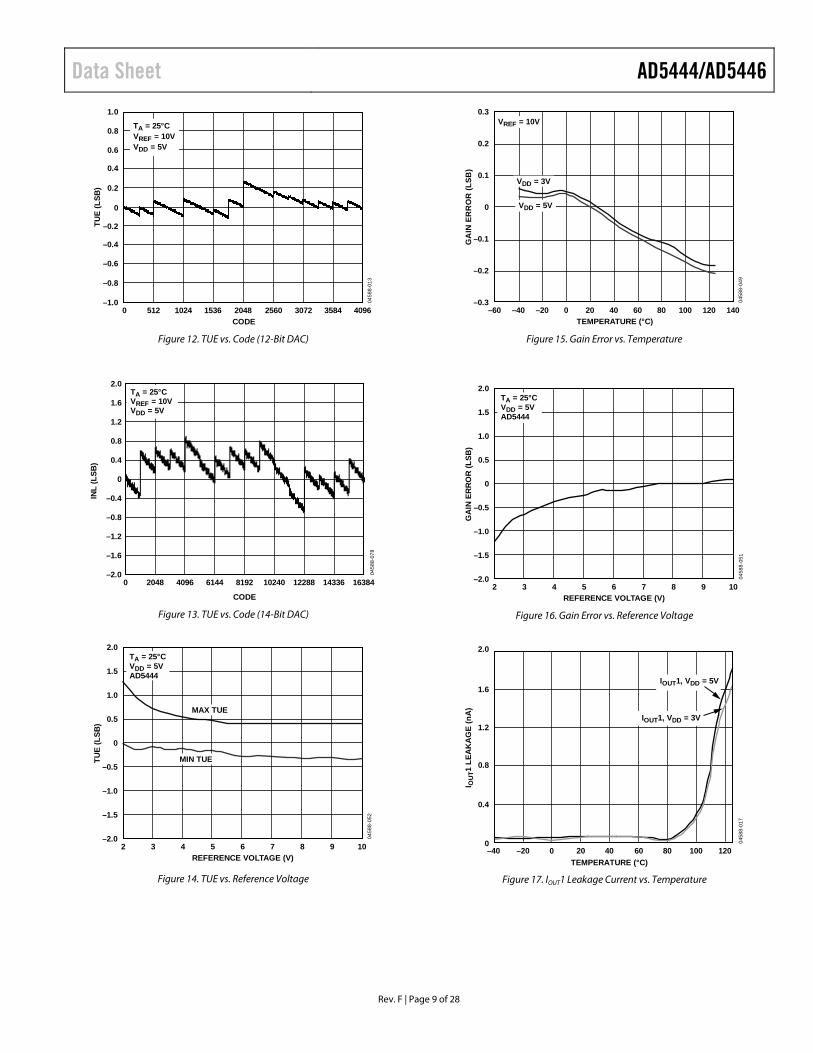
Figure 34. Narrow-Band IMD, fOUT = 20 kHz and 25 kHz, Clock = 1 MHz
–100
–90
–80
–60
–40
–20
0
0 500k
TA = 25°CVREF = 3.5VAD8038 AMP
FREQUENCY (Hz)400k300k200k100k
IMD
(dB
)
0458
8-06
8
–70
–50
–30
–10
Figure 35. Wideband IMD, fOUT = 20 kHz and 25 kHz, Clock = 1 MHz
0458
8-06
9
100 1k 10k 100k 1M
FREQUENCY (Hz)
80
0
70
OU
TPU
TN
OIS
E(n
V/H
z)
TA = 25°CAD8038 AMP
50
60
40
20
30
10
FULL SCALELOADED TO DAC
MIDSCALELOADED TO DAC
ZERO SCALELOADED TO DAC
Figure 36. Output Noise Spectral Density

AD5444/AD5446 Data Sheet
Rev. F | Page 14 of 28
TERMINOLOGY Relative Accuracy or Integral Nonlinearity Relative accuracy or integral nonlinearity is a measure of the maximum deviation from a straight line passing through the endpoints of the DAC transfer function. It is measured after adjusting for zero scale and full scale and is normally expressed in LSBs or as a percentage of full-scale reading.
Differential Nonlinearity Differential nonlinearity is the difference between the measured change and the ideal 1 LSB change between any two adjacent codes. A specified differential nonlinearity of −1 LSB maximum over the operating temperature range ensures monotonicity.
Gain Error Gain error or full-scale error is a measure of the output error between an ideal DAC and the actual device output. For this DAC, ideal maximum output is VREF − 1 LSB. Gain error of the DAC is adjustable to zero with external resistance.
Output Leakage Current Output leakage current is current that flows in the DAC ladder switches when the ladder is turned off. For the IOUT1 line, it can be measured by loading all 0s to the DAC and measuring the IOUT1 current. Minimum current flows in the IOUT2 line when the DAC is loaded with all 1s.
Output Capacitance Capacitance from IOUT1 or IOUT2 to AGND.
Output Current Settling Time The amount of time it takes for the output to settle to a speci-fied level for a full-scale input change. For this device, it is specified with a 100 Ω resistor to ground. The settling time specification includes the digital delay from the SYNC rising edge to the full-scale output change.
Digital-to-Analog Glitch Impulse The amount of charge injected from the digital inputs to the analog output when the inputs change state. This is normally specified as the area of the glitch in either picoamps per second or nanovolts per second, depending upon whether the glitch is measured as a current or voltage signal.
Digital Feedthrough When the device is not selected, high frequency logic activ-ity on the device’s digital inputs can be capacitively coupled through the device to show up as noise on the IOUT1 and IOUT2 pins and, subsequently, into the following circuitry. This noise is digital feedthrough.
Multiplying Feedthrough Error Multiplying feedthrough error is due to capacitive feedthrough from the DAC reference input to the DAC IOUT1 line, when all 0s are loaded to the DAC.
Total Harmonic Distortion (THD) The DAC is driven by an ac reference. The ratio of the rms sum of the harmonics of the DAC output to the fundamental value is the THD. Usually only the lower-order harmonics, such as second to fifth, are included.
1
5432
VVVVV
THD2222
log20+++
=
Digital Intermodulation Distortion Second-order intermodulation (IMD) measurements are the relative magnitudes of the fa and fb tones digitally generated by the DAC and the second-order products at 2fa − fb and 2fb − fa.
Compliance Voltage Range The maximum range of (output) terminal voltage for which the device provides the specified characteristics.
Spurious-Free Dynamic Range (SFDR) The usable dynamic range of a DAC before spurious noise interferes or distorts the fundamental signal. SFDR is the measure of difference in amplitude between the fundamental and the largest harmonically or nonharmonically related spur from dc to full Nyquist bandwidth (half the DAC sampling rate or fS/2). Narrow-band SFDR is a measure of SFDR over an arbitrary window size, in this case 50% of the fundamental. Digital SFDR is a measure of the usable dynamic range of the DAC when the signal is a digitally generated sine wave.

Data Sheet AD5444/AD5446
Rev. F | Page 15 of 28
GENERAL DESCRIPTION DAC SECTION The AD5444/AD5446 are 12-bit and 14-bit current output DACs consisting of segmented (4 bits), inverting R– 2R ladder configurations. A simplified diagram for the 12-bit AD5444 is shown in Figure 37.
2R
S1
2R
S2
2R
S3
2R
S12
2R
DAC DATA LATCHESAND DRIVERS
RRFB
IOUT1
IOUT2
VREF
0446
4-02
9
R R R
Figure 37. Simplified Ladder
The feedback resistor (RFB) has a value of R. The value of R is typically 9 kΩ (7 kΩ minimum, 11 kΩ maximum). If IOUT1 is kept at the same potential as GND, a constant current flows in each ladder leg, regardless of digital input code. Therefore, the input resistance presented at VREF is always constant and nomi-nally of value R. The DAC output (IOUT1) is code-dependent, producing various resistances and capacitances. The external amplifier choice should take into account the variation in impedance generated by the DAC on the amplifiers inverting input node.
Access is provided to the VREF, RFB, and both IOUT terminals of the DAC, making the device extremely versatile and allowing it to be configured in several different operating modes. For example, the device provides unipolar output mode, 4-quadrant multiplication in bipolar mode, and single-supply mode of operation. Note that a matching switch is used in series with the internal RFB. Power must be applied to VDD to achieve continuity when measuring RFB.
CIRCUIT OPERATION Unipolar Mode
Using a single op amp, the AD5444/AD5446 can easily be configured to provide 2-quadrant multiplying operation or a unipolar output voltage swing, as shown in Figure 38.
When an output amplifier is connected in unipolar mode, the output voltage is given by
REFnOUT VDV 2
where:
D is the fractional representation of the digital word loaded to the DAC:
D = 0 to 4095 (12-bit AD5444) D = 0 to 16383 (14-bit AD5446)
n is the number of bits.
Note that the output voltage polarity is opposite to the VREF polarity for dc reference voltages.
This DAC is designed to operate with either negative or positive reference voltages. The VDD power pin is used by the internal digital logic only to drive the on and off states of the DAC switches. The DAC is also designed to accommodate ac refer-ence input signals in the range of −10 V to +10 V. With a fixed +10 V reference, the circuit shown in Figure 38 provides a unipolar 0 V to −10 V output voltage swing. When VIN is an ac signal, the circuit performs 2-quadrant multiplication. Table 5 shows the relationship between digital code and expected output voltage for unipolar operation.
Table 5. Unipolar Code Digital Input Analog Output (V) 1111 1111 1111 −VREF (4095/4096) 1000 0000 0000 −VREF (2048/4096) = −VREF/2 0000 0000 0001 −VREF (1/4096) 0000 0000 0000 −VREF (0/4096) = 0
AD5444/AD5446
0458
8-03
0
NOTES1. R1 AND R2 USED ONLY IF GAIN ADJUSTMENT IS REQUIRED.2. C1 PHASE COMPENSATION (1pF TO 2pF) MAY BE REQUIRED, IF A1 IS A HIGH SPEED AMPLIFIER.
IOUT1
IOUT2VREF
VDD
C1
A1
VOUT = 0V TO –VREF
AGND
R2
VDD
VREF
SDINSCLKSYNC
MICROCONTROLLER
RFB
R1
Figure 38. Unipolar Operation

AD5444/AD5446 Data Sheet
Rev. F | Page 16 of 28
Bipolar Operation
In some applications, it may be necessary to generate a full 4-quadrant multiplying operation, or a bipolar output swing. This can easily be accomplished by using another external amplifier and some external resistors, as shown in Figure 39. In this circuit, the second amplifier (A2) provides a gain of 2. Biasing the external amplifier with an offset from the reference voltage results in a full 4-quadrant multiplying operation. The transfer function of this circuit shows that both negative and positive output voltages are created as the input data (D) is incremented from code zero (VOUT = −VREF) to midscale (VOUT − 0 V) to full scale (VOUT = +VREF)
REFnREFOUT VD
VV −
×= −12
where:
D is the fractional representation of the digital word loaded to the DAC:
D = 0 to 4095 (12-bit AD5444) D = 0 to 16383 (14-bit AD5446)
n is the resolution of the DAC.
When VIN is an ac signal, the circuit performs 4-quadrant multiplication.
Table 6 shows the relationship between digital code and the expected output voltage for bipolar operation.
Table 6. Bipolar Code Digital Input Analog Output (V) 1111 1111 1111 +VREF (2047/2048) 1000 0000 0000 0 0000 0000 0001 −VREF (2047/2048) 0000 0000 0000 −VREF (0/2048)
Stability
In the current-to-voltage (I-to-V) configuration, the IOUT1of the DAC and the inverting node of the op amp must be connected as closely as possible, and proper PCB layout techniques must be employed. Because every code change corresponds to a step function, gain peaking can occur if the op amp has limited GBP and excessive parasitic capacitance exists at the inverting node. This parasitic capacitance introduces a pole into the open-loop response that can cause ringing or instability in the closed-loop applications circuit.
An optional compensation capacitor (C1) can be added in parallel with RFB for stability, as shown in Figure 38 and Figure 39. Too small a value for C1 can produce ringing at the output, while too large a value can adversely affect the settling time. C1 should be found empirically, but 1 pF to 2 pF is generally adequate for the compensation.
0458
8-03
1
IOUT1
IOUT2
AD5444/AD5446VREF
VDD
C1
A1
VOUT = –VREF TO +VREF
AGND
R2
VDD
VREF ±10V
SDINSCLKSYNC
MICROCONTROLLER
A2
R410kΩ
R520kΩ
NOTES1. R1 AND R2 USED ONLY IF GAIN ADJUSTMENT IS REQUIRED.
ADJUST R1 FOR VOUT = 0V WITH CODE 10000000 LOADED TO DAC.2. MATCHING AND TRACKING IS ESSENTIAL FOR RESISTOR PAIRS
3. C1 PHASE COMPENSATION (1pF TO 2pF) MAY BE REQUIRED, IF A1/A2 IS A HIGH SPEED AMPLIFIER.
R3 AND R4.
R320kΩ
R1RFB
Figure 39. Bipolar Operation (4-Quadrant Multiplication)

Data Sheet AD5444/AD5446
Rev. F | Page 17 of 28
SINGLE-SUPPLY APPLICATIONS Voltage Switching Mode of Operation
Figure 40 shows the AD5444/AD5446 DACs operating in the voltage switching mode. The reference voltage (VIN) is applied to the IOUT1 pin, IOUT2 is connected to AGND, and the output voltage is available at the VREF terminal. In this configuration, a positive reference voltage results in a positive output voltage, making single-supply operation possible. The output from the DAC is voltage at a constant impedance (the DAC ladder resistance). Therefore, an op amp is necessary to buffer the output voltage. The reference input no longer sees a constant input impedance but rather one that varies with code, so the voltage input should be driven from a low impedance source.
0458
8-03
2
NOTES1. ADDITIONAL PINS OMITTED FOR CLARITY.2. C1 PHASE COMPENSATION (1pF TO 2pF) MAY BE REQUIRED, IF A1 IS A HIGH SPEED AMPLIFIER.
IOUT1
GND
VOUT
R2
VIN
RFB VDD
VREF
R1VDD
Figure 40. Single-Supply Voltage Switching Mode Operation
It is important to note that, with this configuration, VIN is lim-ited to low voltages, because the switches in the DAC ladder do not have the same source-drain drive voltage. As a result, their on resistance differs, which degrades the integral linearity of the DAC. In addition, VIN must not go negative by more than 0.3 V, or an internal diode turns on, exceeding the maximum ratings of the device. In this type of application, the full range of the multiplying capability of the DAC is lost.
ADDING GAIN In applications in which the output voltage is required to be greater than VIN, gain can be added with an additional external amplifier, or it can be achieved in a single stage. It is important to take into consideration the effect of the temperature coeffi-cients of the thin film resistors of the DAC. Simply placing a resistor in series with the RFB resistor can cause mismatches in the temperature coefficients and result in larger gain tempera-ture coefficient errors. Instead, increase the gain of the circuit by using the recommended configuration shown in Figure 41. R1, R2, and R3 must all have similar temperature coefficients, but they need not match the temperature coefficients of the DAC. This approach is recommended in circuits where gains of greater than 1 are required. Note that RFB >> R2||R3 and a gain error percentage of 100 × (R2||R3)/RFB must be taken into consideration.
NOTES1. ADDITIONAL PINS OMITTED FOR CLARITY.2. C1 PHASE COMPENSATION (1pF TO 2pF) MAY BE REQUIRED, IF A1 IS A HIGH SPEED AMPLIFIER.
VDD RFB
IOUT1
IOUT2
C1
VOUT
GND
VDD
VREF
0458
8-03
4
GAIN =
R1 =
R2 + R3R2
R2R3R2 + R3
R1VIN
R3
R2
Figure 41. Increasing Gain of Current Output DAC
DIVIDER OR PROGRAMMABLE GAIN ELEMENT Current-steering DACs are very flexible and lend themselves to many different applications. If this type of DAC is connected as the feedback element of an op amp and RFB is used as the input resistor, as shown in Figure 42, then the output voltage is inversely proportional to the digital input fraction, D.
For D = 1 − 2−n, the output voltage is
VOUT = −VIN/D = −VIN/(1 − 2−n)
0458
8-03
5
NOTES:1. ADDITIONAL PINS OMITTED FOR CLARITY.
IOUT1
GND
VOUT
VIN
RFB VDD
VREF
VDD
Figure 42. Current-Steering DAC Used as a Divider
or Programmable Gain Element
As D is reduced, the output voltage increases. For small values of the digital fraction (D), it is important to ensure that the amplifier does not saturate and the required accuracy is met. For example, an 8-bit DAC driven with the binary code 0x10 (0001 0000), that is, 16 decimal, in the circuit of Figure 42, should cause the output voltage to be 16 × VIN. However, if the DAC has a linearity specification of ±0.5 LSB, then D can, in fact, have a weight in the range of 15.5/256 to 16.5/256, so the possible output voltage is in the range 15.5 VIN to 16.5 VIN. This is an error of 3%, even though the DAC itself has a maximum error of 0.2%.

AD5444/AD5446 Data Sheet
Rev. F | Page 18 of 28
DAC leakage current is also a potential error source in divider circuits. The leakage current must be counterbalanced by an opposite current supplied from the op amp through the DAC. Because only a fraction (D) of the current into the VREF terminal is routed to the IOUT1 terminal, the output voltage has to change, as follows:
Output Error Voltage due to DAC Leakage = (Leakage × R)/D
where R is the DAC resistance at the VREF terminal.
For a DAC leakage current of 10 nA, R equal to 10 kΩ, and a gain (1/D) of 16, the error voltage is 1.6 mV.
AMPLIFIER SELECTION The primary requirement for the current-steering mode is an amplifier with low input bias currents and low input offset voltage. The input offset voltage of an op amp is multiplied by the variable gain (due to the code-dependent output resistance of the DAC) of the circuit. A change in this noise gain between two adjacent digital fractions produces a step change in the output voltage due to the amplifier’s input offset voltage. This output voltage change is superimposed upon the desired change in output between the two codes and gives rise to a differential linearity error, which, if large enough, can cause the DAC to be nonmonotonic.
The input bias current of an op amp also generates an offset at the voltage output as a result of the bias current flowing in the feedback resistor, RFB. Most op amps have input bias currents low enough to prevent any significant errors in 12-bit applications.
Common-mode rejection of the op amp is important in voltage switching circuits because it produces a code-dependent error at the voltage output of the circuit. Most op amps have adequate common-mode rejection for use at 8-bit, 10-bit, and 12-bit resolutions.
Provided that the DAC switches are driven from true wideband low impedance sources (VIN and AGND), they settle quickly. Consequently, the slew rate and settling time of a voltage switching DAC circuit is determined largely by the output op amp. To obtain minimum settling time in this configuration, it is impor-tant to minimize capacitance at the VREF node (voltage output node in this application) of the DAC. This is done by using low input, capacitance buffer amplifiers and careful board design.
Most single-supply circuits include ground as part of the analog signal range, which, in turn, requires an amplifier that can handle rail-to-rail signals. A large range of single-supply amplifiers is available from Analog Devices, Inc. (see Table 8 and Table 9 for suitable suggestions).
REFERENCE SELECTION When selecting a reference for use with the AD5444/AD5446 current output DAC, pay attention to the output voltage tem-perature coefficient specification. This parameter affects not only the full-scale error but can also affect the linearity (INL and DNL) performance. The reference temperature coefficient should be consistent with the system accuracy specifications. For example, an 8-bit system required to hold its overall speci-fication to within 1 LSB over the temperature range 0°C to 50°C dictates that the maximum system drift with temperature should be less than 78 ppm/°C.
A 12-bit system with the same temperature range to overall specification within 2 LSBs requires a maximum drift of 10 ppm/°C. By choosing a precision reference with low output temperature coefficient, this error source can be minimized. Table 7 suggests some of the dc references available from Analog Devices that are suitable for use with this range of current output DACs.

Data Sheet AD5444/AD5446
Rev. F | Page 19 of 28
Table 7. Suitable Analog Devices Precision References
Part No. Output Voltage (V) Initial Tolerance Accuracy (%)
Temperature Drift Coefficient (ppm/°C) ISS (mA) Output Noise (µV p-p) Package
ADR01 10 0.05 3 1 20 SOIC-8 ADR01 10 0.05 9 1 20 TSOT-23, SC70 ADR02 5 0.06 3 1 10 SOIC-8 ADR02 5 0.06 9 1 10 TSOT-23, SC70 ADR03 2.5 0.10 3 1 6 SOIC-8 ADR03 2.5 0.10 9 1 6 TSOT-23, SC70 ADR06 3 0.10 3 1 10 SOIC-8 ADR06 3 0.10 9 1 10 TSOT-23, SC70 ADR431 2.5 0.04 3 0.8 3.5 SOIC-8 ADR435 5 0.04 3 0.8 8 SOIC-8 ADR391 2.5 0.16 9 0.12 5 TSOT-23 ADR395 5 0.10 9 0.12 8 TSOT-23
Table 8. Suitable Analog Devices Precision Op Amps Part No. Supply Voltage (V) VOS (Max) (µV) IB (Max) (nA) 0.1 Hz to 10 Hz Noise (µV p-p) Supply Current (µA) Package OP97 ±2 to ±20 25 0.1 0.5 600 SOIC-8 OP1177 ±2.5 to ±15 60 2 0.4 500 MSOP, SOIC-8 AD8551 2.7 to 5 5 0.05 1 975 MSOP, SOIC-8 AD8603 1.8 to 6 50 0.001 2.3 50 TSOT AD8628 2.7 to 6 5 0.1 0.5 850 TSOT, SOIC-8
Table 9. Suitable Analog Devices High Speed Op Amps
Part No. Supply Voltage (V) BW @ ACL (Typ) (MHz)
Slew Rate (Typ) (V/µs) VOS (Max) (µV) IB (Max) (nA) Package
AD8065 5 to 24 145 180 1500 0.006 SOIC-8, SOT-23, MSOP AD8021 ±2.25 to ±12 490 120 1000 10500 SOIC-8, MSOP AD8038 3 to 12 350 425 3000 750 SOIC-8, SC70-5 AD9631 ±3 to ±6 320 1300 10,000 7000 SOIC-8

AD5444/AD5446 Data Sheet
Rev. F | Page 20 of 28
SERIAL INTERFACE The AD5444/AD5446 have an easy-to-use, 3-wire interface that is compatible with SPI, QSPI, MICROWIRE, and DSP inter-face standards. Data is written to the device in 16-bit words. This 16-bit word consists of two control bits, 12 data bits or 14 data bits, as shown in Figure 43 and Figure 44. The AD5446 uses all 14 bits of DAC data while AD5444 uses 12 bits and ignores the 2 LSBs.
Control Bit C1 and Control Bit C0 allow the user to load and update the new DAC code and to change the active clock edge. By default, the shift register clocks data on the falling edge, but this can be changed via the control bits. If changed, the DAC core is inoperative until the next data frame. A power cycle resets this back to the default condition. On-chip, power-on reset circuitry ensures the device powers on with zero scale loaded to the DAC register and the IOUT line.
Table 10. DAC Control Bits C1 C0 Function Implemented 0 0 Load and update (power-on default) 0 1 Disable SDO 1 0 No operation 1 1 Clock data to shift register on rising edge
SYNC Function
SYNC is an edge-triggered input that acts as a frame synchroni-zation signal. Data can be transferred into the device only while SYNC is low. To start the serial data transfer, SYNC should be taken low, observing the minimum SYNC falling to the SCLK falling edge setup time, t4. To minimize the power consumption of the device, the interface powers up fully only when the device is being written to, that is, on the falling edge of SYNC.
The SCLK and DIN input buffers are powered down on the rising edge of SYNC.
After the falling edge of the 16th SCLK pulse, bring SYNC high to transfer data from the input shift register to the DAC register.
Daisy-Chain Mode
Daisy-chain mode is the default power-on mode. To disable the daisy-chain function, write 01 to the control word. In daisy-chain mode, the internal gating on the SCLK is disabled. The SCLK is continuously applied to the input shift register when SYNC is low. If more than 16 clock pulses are applied, the data ripples out of the shift register and appears on the SDO line. This data is clocked out on the rising edge of the SCLK (this is the default; use the control word to change the active edge) and is valid for the next device on the falling edge (default). By connecting this line to the SDIN input on the next device in the chain, a multidevice interface is constructed. Sixteen clock pulses are required for each device in the system. Therefore, the total number of clock cycles must equal 16 N, where N is the number of devices in the chain.
When the serial transfer to all devices is complete, SYNC should be taken high. This prevents any further data from being clocked into the shift register. A burst clock containing the exact number of clock cycles can be used, and SYNC can be taken high some time later. After the rising edge of SYNC, data is automatically transferred from each device’s input register to the addressed DAC.
When the control bits = 10, the device is in no operation mode. This can be useful in daisy-chain applications where the user does not want to change the settings of a particular DAC in the chain. Simply write 10 to the control bits for that DAC and the following data bits are ignored.
0458
8-03
7
DB0 (LSB)DB15 (MSB)
DB7 DB6 DB5 DB4 DB3 DB2 DB0DB1C1 C0 DB11 DB10 DB8DB9 XX
CONTROL BITSDATA BITS
Figure 43. AD5444 12-Bit Input Shift Register Contents
0458
8-03
8
DB0 (LSB)DB15 (MSB)
DB9 DB8 DB7 DB6 DB5 DB4 DB2DB3C1 C0 DB13 DB12 DB10DB11 DB0DB1
CONTROL BITSDATA BITS
Figure 44. AD5446 14-Bit Input Shift Register Contents

Data Sheet AD5444/AD5446
Rev. F | Page 21 of 28
MICROPROCESSOR INTERFACING Microprocessor interfacing to the AD5444/AD5446 DAC is through a serial bus that uses standard protocol compatible with microcontrollers and DSP processors. The communica-tions channel is a 3-wire interface consisting of a clock signal, a data signal, and a synchronization signal. The AD5444/AD5446 requires a 16-bit word, with the default being data valid on the falling edge of SCLK, but this can be changed using the control bits in the data-word.
ADSP-2191M to AD5444/AD5446 Interface
The ADSP-2191M DSP is easily interfaced to the AD5444/AD5446 DAC without the need for extra glue logic. Figure 45 is an example of an SPI interface between the DAC and the ADSP-2191M. SCK of the DSP drives the serial clock line, SCLK. SYNC is driven from one of the port lines, in this case SPIxSEL.
SCLKSCK
SYNCSPIxSEL
SDINMOSI
ADSP-2191M*
*ADDITIONAL PINS OMITTED FOR CLARITY.
AD5444/AD5446*
0458
8-07
4
Figure 45. ADSP-2191M SPI to AD5444/AD5446 Interface
A serial interface between the DAC and DSP SPORT is shown in Figure 46. In this interface example, SPORT0 is used to trans-fer data to the DAC shift register. Transmission is initiated by writing a word to the Tx register after the SPORT has been enabled. In a write sequence, data is clocked out on each rising edge of the DSP serial clock and clocked into the DAC input shift register on the falling edge of its SCLK. The update of the DAC output takes place on the rising edge of the SYNC signal.
SCLKSCLK
SYNCTFS
SDINDT
ADSP-2191M*
*ADDITIONAL PINS OMITTED FOR CLARITY. 0458
8-08
2
AD5444/AD5446*
Figure 46. ADSP-2191M to AD5444/AD5446 Interface
Communication between two devices at a given clock speed is possible when the following specifications are compatible: frame sync delay and frame sync setup-and-hold, data delay and data setup-and-hold, and SCLK width. The DAC interface expects a t4 (SYNC falling edge to SCLK falling edge setup time) of 13 ns minimum. See the user manuals at www.analog.com/adsp-21xx-processor-manuals for information on clock and frame sync frequencies for the SPORT register.
Table 11 shows the setup for the SPORT control register.
Table 11. SPORT Control Register Setup Name Setting Description TFSW 1 Alternate framing INVTFS 1 Active low frame signal DTYPE 00 Right-justify data ISCLK 1 Internal serial clock TFSR 1 Frame every word ITFS 1 Internal framing signal SLEN 1111 16-bit data-word
Blackfin to AD5444/AD5446 Interface
The ADSP-BF504 to ADSP-BF592 family of processors has an SPI-compatible port that enables the processor to communicate with SPI-compatible devices. Figure 47 shows a serial interface between the ADSP-BF504 to ADSP-BF592 family (the ADSP-BF534 shown as an example) and the AD5444/AD5446 DAC. In this configuration, data is transferred through the MOSI (master output/slave input) pin. SYNC is driven by the SPI chip select pin, which is a reconfigured programmable flag pin.
SCLKSCK
SYNCSPISELx
SDINMOSI
ADSP-BF534*
*ADDITIONAL PINS OMITTED FOR CLARITY.
AD5444/AD5446*
0458
8-03
9
Figure 47. ADSP-BF534 to AD5444/AD5446 Interface
The ADSP-BF534 processor incorporates channel synchronous serial ports (SPORT). A serial interface between the DAC and the DSP SPORT is shown in Figure 48. When the SPORT is enabled, initiate transmission by writing a word to the Tx register. The data is clocked out on each rising edge of the DSPs serial clock and clocked into the DAC input shift register on the falling edge of its SCLK. The DAC output is updated by using the transmit frame synchronization (TFS) line to provide a SYNC signal.
SCLKSCLK
SYNCTFSx
SDINDTx
ADSP-BF534*
*ADDITIONAL PINS OMITTED FOR CLARITY. 0458
8-04
0AD5444/AD5446*
Figure 48. ADSP-BF534 to AD5444/AD5446 Interface

AD5444/AD5446 Data Sheet
Rev. F | Page 22 of 28
80C51/80L51 to AD5444/AD5446 Interface
A serial interface between the DAC and the 80C51/80L51 is shown in Figure 49. TxD of the 80C51/80L51 drives SCLK of the DAC serial interface, while RxD drives the serial data line, SDIN. P1.1 is a bit-programmable pin on the serial port and is used to drive SYNC. When data is to be transmitted to the switch, P1.1 is taken low. The 80C51/80L51 transmits data only in 8-bit bytes; therefore, only eight falling clock edges occur in the transmit cycle. To load data correctly to the DAC, P1.1 is left low after the first eight bits are transmitted, and a second write cycle is initiated to transmit the second byte of data.
Data on RxD is clocked out of the microcontroller on the rising edge of TxD and is valid on the falling edge. As a result, no glue logic is required between the DAC and microcontroller inter-face. P1.1 is taken high following the completion of this cycle. The 80C51/80L51 provides the LSB of its SBUF register as the first bit in the data stream. The DAC input register requires its data with the MSB as the first bit received. The transmit routine should take this into account.
SCLKTxD8051*
SYNCP1.1
SDINRxD
*ADDITIONAL PINS OMITTED FOR CLARITY 0458
8-04
1
AD5444/AD5446*
Figure 49. 80C51/80L51 to AD5444/AD5446 Interface
MC68HC11 Interface to AD5444/AD5446 Interface
Figure 50 is an example of a serial interface between the DAC and the MC68HC11 microcontroller. The serial peripheral interface (SPI) on the MC68HC11 is configured for master mode (MSTR) = 1, clock polarity bit (CPOL) = 0, and the clock phase bit (CPHA) = 1. The SPI is configured by writing to the SPI control register (SPCR); see the 68HC11 User Manual. SCK of the 68HC11 drives the SCLK of the DAC interface, the MOSI output drives the serial data line (SDIN) of the AD5444/AD5446.
The SYNC signal is derived from a port line (PC7). When data is being transmitted to the AD5444/AD5446, the SYNC line is taken low (PC7). Data appearing on the MOSI output is valid on the falling edge of SCK. Serial data from the 68HC11 is transmitted in 8-bit bytes with only eight falling clock edges occurring in the transmit cycle. Data is transmitted MSB first. To load data to the DAC, PC7 is left low after the first eight bits are transferred, and a second serial write operation is performed to the DAC. PC7 is taken high at the end of this procedure.
SCLKSCK
AD5444/AD5446*SYNCPC7
SDINMOSI
MC68HC11*
*ADDITIONAL PINS OMITTED FOR CLARITY 0458
8-04
2
Figure 50. MC68HC11 to AD5444/AD5446 Interface
If the user wants to verify the data previously written to the input shift register, the SDO line can be connected to MISO of the MC68HC11, and, with SYNC low, the shift register clocks data out on the rising edges of SCLK.
MICROWIRE to AD5444/AD5446 Interface
Figure 51 shows an interface between the DAC and any MICROWIRE-compatible device. Serial data is shifted out on the falling edge of the serial clock, SK, and is clocked into the DAC input shift register on the rising edge of SK, which corresponds to the falling edge of the DAC SCLK.
SCLKSK
MICROWIRE*
SYNCCS
SDINSO
*ADDITIONAL PINS OMITTED FOR CLARITY 0458
8-04
3
AD5444/AD5446*
Figure 51. MICROWIRE to AD5444/AD5446 Interface
PIC16C6x/7x to AD5444/AD5446 Interface
The PIC16C6x/7x synchronous serial port (SSP) is configured as an SPI master with the clock polarity bit (CKP) = 0. This is done by writing to the synchronous serial port control register (SSPCON); see the PIC16/17 Microcontroller User Manual.
In this example, I/O port RA1 is used to provide a SYNC signal and enable the serial port of the DAC. This micro-controller transfers only eight bits of data during each serial transfer operation; therefore, two consecutive write operations are required. Figure 52 shows the connection diagram.
SCLKSCK/RC3
PIC16C6x/7x*
SYNCRA1
SDINSDI/RC4
*ADDITIONAL PINS OMITTED FOR CLARITY 0458
8-04
4AD5444/AD5446*
Figure 52. PIC16C6x/7x to AD5444/AD5446 Interface

Data Sheet AD5444/AD5446
Rev. F | Page 23 of 28
PCB LAYOUT AND POWER SUPPLY DECOUPLING In any circuit where accuracy is important, careful considera-tion of the power supply and ground return layout helps to ensure the rated performance. The printed circuit boards on which the AD5444/AD5446 are mounted should be designed so the analog and digital sections are separated and confined to certain areas of the board. If the DACs are in systems in which multiple devices require a AGND-to-DGND connection, the connection should be made at one point only. The star ground point should be established as close as possible to the devices.
The DAC should have ample supply bypassing of 10 µF in parallel with 0.1 µF on the supply located as close to the pack-age as possible, ideally right up against the device. The 0.1 µF capacitor should have low effective series resistance (ESR) and effective series inductance (ESI), like the common ceramic types that provide a low impedance path to ground at high frequencies, to handle transient currents due to internal logic switching. Low ESR, 1 µF to 10 µF tantalum or electrolytic capacitors should also be applied at the supplies to minimize transient disturbance and filter out low frequency ripple.
Fast switching signals such as clocks should be shielded with digital ground to avoid radiating noise to other parts of the board, and should never be run near the reference inputs.
Avoid crossover of digital and analog signals. Traces on oppo-site sides of the board should run at right angles to each other. This reduces the effects of feedthrough throughout the board.
A microstrip technique, by far the best, is not always possible with a double-sided board. In this technique, the component side of the board is dedicated to the ground plane, while signal traces are placed on the solder side.
It is good practice to employ compact, minimum lead-length PCB layout design. Leads to the input should be as short as possible to minimize IR drops and stray inductance.
The PCB metal traces between VREF and RFB should also be matched to minimize gain error. To maximize high frequency performance, the I-to-V amplifier should be located as close to the device as possible.

AD5444/AD5446 Data Sheet
Rev. F | Page 24 of 28
OVERVIEW OF CURRENT OUTPUT DEVICES Table 12. Part Number Resolution (Bits) Number of DACs INL (LSB) Interface Package1 Features AD5424 8 1 ±0.25 Parallel RU-16, CP-20 10 MHz BW, 17 ns CS pulse width
AD5426 8 1 ±0.25 Serial RM-10 10 MHz BW, 50 MHz serial AD5428 8 2 ±0.25 Parallel RU-20 10 MHz BW, 17 ns CS pulse width
AD5429 8 2 ±0.25 Serial RU-10 10 MHz BW, 50 MHz serial AD5450 8 1 ±0.25 Serial UJ-8 12 MHz BW, 50 MHz serial AD5432 10 1 ±0.5 Serial RM-10 10 MHz BW, 50 MHz serial AD5433 10 1 ±0.5 Parallel RU-20, CP-20 10 MHz BW, 17 ns CS pulse width
AD5439 10 2 ±0.5 Serial RU-16 10 MHz BW, 50 MHz serial AD5440 10 2 ±0.5 Parallel RU-24 10 MHz BW, 17 ns CS pulse width
AD5451 10 1 ±0.25 Serial UJ-8 12 MHz BW, 50 MHz serial AD5443 12 1 ±1 Serial RM-10 10 MHz BW, 50 MHz serial AD5444 12 1 ±0.5 Serial RM-10 12 MHz BW, 50 MHz serial interface AD5415 12 2 ±1 Serial RU-24 10 MHz BW, 50 MHz serial AD5405 12 2 ±1 Parallel CP-40 10 MHz BW, 17 ns CS pulse width
AD5445 12 2 ±1 Parallel RU-20, CP-20 10 MHz BW, 17 ns CS pulse width
AD5447 12 2 ±1 Parallel RU-24 10 MHz BW, 17 ns CS pulse width
AD5449 12 2 ±1 Serial RU-16 10 MHz BW, 50 MHz serial AD5452 12 1 ±0.5 Serial UJ-8, RM-8 12 MHz BW, 50 MHz serial AD5446 14 1 ±1 Serial RM-10 12 MHz BW, 50 MHz serial AD5453 14 1 ±2 Serial UJ-8, RM-8 12 MHz BW, 50 MHz serial AD5553 14 1 ±1 Serial RM-8 4 MHz BW, 50 MHz serial clock AD5556 14 1 ±1 Parallel RU-28 4 MHz BW, 20 ns WR pulse width
AD5555 14 2 ±1 Serial RM-8 4 MHz BW, 50 MHz serial clock AD5557 14 2 ±1 Parallel RU-38 4 MHz BW, 20 ns WR pulse width
AD5543 16 1 ±2 Serial RM-8 4 MHz BW, 50 MHz serial clock AD5546 16 1 ±2 Parallel RU-28 4 MHz BW, 20 ns WR pulse width
AD5545 16 2 ±2 Serial RU-16 4 MHz BW, 50 MHz serial clock AD5547 16 2 ±2 Parallel RU-38 4 MHz BW, 20 ns WR pulse width 1 RU = TSSOP, CP = LFCSP, RM = MSOP, UJ = TSOT.

Data Sheet AD5444/AD5446
Rev. F | Page 25 of 28
OUTLINE DIMENSIONS
COMPLIANT TO JEDEC STANDARDS MO-187-BA 0917
09-A
6°0°
0.700.550.40
5
10
1
6
0.50 BSC
0.300.15
1.10 MAX
3.103.002.90
COPLANARITY0.10
0.230.13
3.103.002.90
5.154.904.65
PIN 1IDENTIFIER
15° MAX0.950.850.75
0.150.05
Figure 53. 10-Lead Mini Small Outline Package [MSOP]
(RM-10) Dimensions shown in millimeters
ORDERING GUIDE Model1 Resolution (Bits) INL (LSB) Temperature Range Package Description Package Option Branding AD5444YRM 12 ±0.5 −40°C to +125°C 10-Lead MSOP RM-10 D27 AD5444YRMZ 12 ±0.5 −40°C to +125°C 10-Lead MSOP RM-10 D6X AD5444YRMZ-REEL7 12 ±0.5 −40°C to +125°C 10-Lead MSOP RM-10 D6X AD5446YRM 14 ±2 −40°C to +125°C 10-Lead MSOP RM-10 D28 AD5446YRMZ 14 ±2 −40°C to +125°C 10-Lead MSOP RM-10 D7Z AD5446YRMZ-RL7 14 ±2 −40°C to +125°C 10-Lead MSOP RM-10 D7Z EV-AD5443/46/53SDZ Evaluation Board 1 Z = RoHS Compliant Part.

AD5444/AD5446 Data Sheet
Rev. F | Page 26 of 28
NOTES

Data Sheet AD5444/AD5446
Rev. F | Page 27 of 28
NOTES

AD5444/AD5446 Data Sheet
Rev. F | Page 28 of 28
NOTES
©2004–2016 Analog Devices, Inc. All rights reserved. Trademarks and registered trademarks are the property of their respective owners. D04588-0-2/16(F)