Embed Size (px)
Citation preview

FEATURESANALOG FEATURES
24 Bits No Missing Codes 22 Bits Effective Resolution at 10Hz
− Low Noise: 75nV PGA From 1 to 128 Precision On-Chip Voltage Reference
− Accuracy: 0.2%− Drift: 5ppm/ °C
8 Differential/Single-Ended Channels On-Chip Offset/Gain Calibration Offset Drift: 0.1ppm/ °C Gain Drift: 0.5ppm/ °C On-Chip Temperature Sensor Selectable Buffer Input Burnout Detect 16-Bit Monotonic Voltage DACS:
− Quad Voltage DACs (MSC1211, MSC1212)− Dual Voltage DACs (MSC1213, MSC1214)
DIGITAL FEATURESMicrocontroller Core 8051-Compatible High-Speed Core
− 4 Clocks per Instruction Cycle DC to 40MHz at +85 C Single Instruction 100ns Dual Data Pointer
Memory Up To 32kB Flash Memory Flash Memory Partitioning Endurance 1M Erase/Write Cycles,
100-Year Data Retention In-System Serially Programmable External Program/Data Memory (64kB) 1,280 Bytes Data SRAM Flash Memory Security 2kB Boot ROM Programmable Wait State Control
Peripheral Features 34 I/O Pins Additional 32-Bit Accumulator Three 16-Bit Timer/Counters System Timers Programmable Watchdog Timer Full-Duplex Dual USARTs Master/Slave SPI with DMA Multi-master I 2C (MSC1211 and MSC1213) 16-Bit PWM Power Management Control Internal Clock Divider Idle Mode Current < 200 µA Stop Mode Current < 100nA Programmable Brownout Reset Programmable Low-Voltage Detect 24 Interrupt Sources Two Hardware Breakpoints
GENERAL FEATURES
Pin-Compatible with MSC1210 Package: TQFP-64 Low Power: 4mW Industrial Temperature Range:
−40°C to +125°C Power Supply: 2.7V to 5.25V
APPLICATIONS Industrial Process Control Instrumentation Liquid/Gas Chromatography Blood Analysis Smart Transmitters Portable Instruments Weigh Scales Pressure Transducers Intelligent Sensors Portable Applications DAS Systems
SBAS323G − JUNE 2004 − REVISED OCTOBER 2007
!" # $%
www.ti.com
Copyright 2004−2007, Texas Instruments Incorporated
Please be aware that an important notice concerning availability, standard warranty, and use in critical applications of Texas Instrumentssemiconductor products and disclaimers thereto appears at the end of this data sheet.
I2C is a trademark of Philips corporation. SPI is a trademark of Motorola Inc. All other trademarks are the property of their respective owners.
&'()*'+ ) ,$ - , .-/ 0 -,$ . , . $ , )1 *-$ %0- . % - , .$0
SBAS323G − JUNE 2004 − REVISED OCTOBER 2007
www.ti.com
2
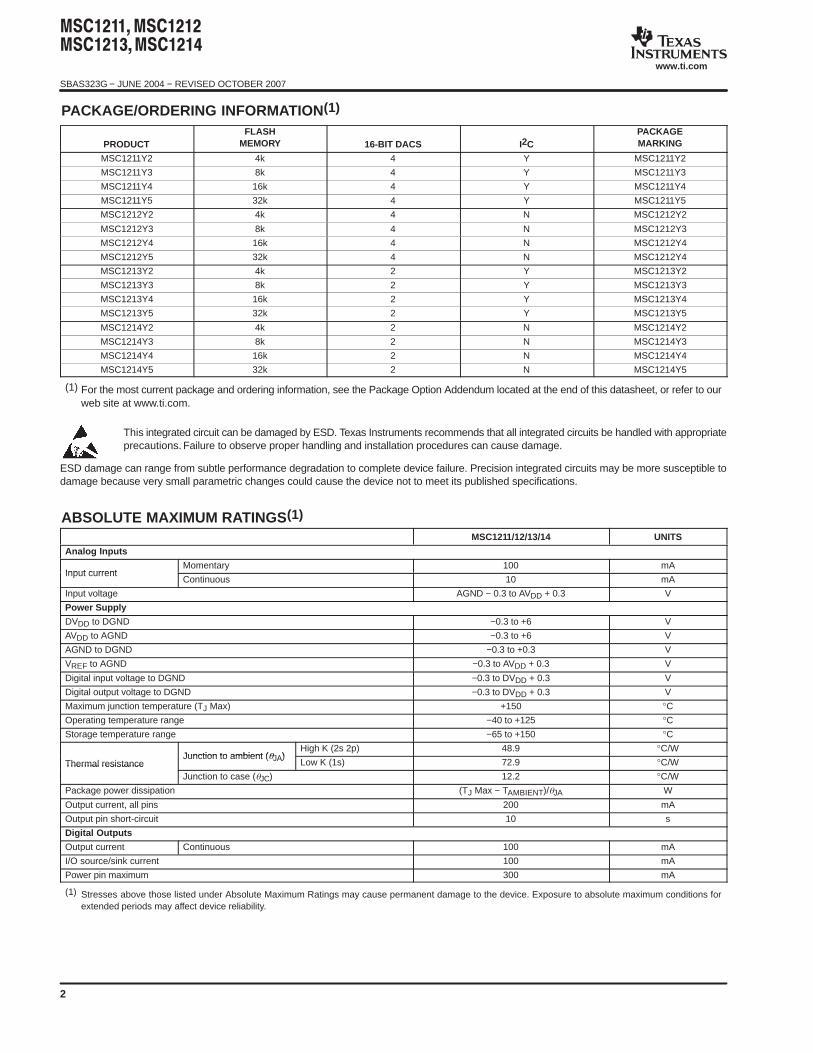
PACKAGE/ORDERING INFORMATION (1)
PRODUCTFLASH
MEMORY 16-BIT DACS I2CPACKAGEMARKING
MSC1211Y2 4k 4 Y MSC1211Y2
MSC1211Y3 8k 4 Y MSC1211Y3
MSC1211Y4 16k 4 Y MSC1211Y4
MSC1211Y5 32k 4 Y MSC1211Y5
MSC1212Y2 4k 4 N MSC1212Y2
MSC1212Y3 8k 4 N MSC1212Y3
MSC1212Y4 16k 4 N MSC1212Y4
MSC1212Y5 32k 4 N MSC1212Y4
MSC1213Y2 4k 2 Y MSC1213Y2
MSC1213Y3 8k 2 Y MSC1213Y3
MSC1213Y4 16k 2 Y MSC1213Y4
MSC1213Y5 32k 2 Y MSC1213Y5
MSC1214Y2 4k 2 N MSC1214Y2
MSC1214Y3 8k 2 N MSC1214Y3
MSC1214Y4 16k 2 N MSC1214Y4
MSC1214Y5 32k 2 N MSC1214Y5
(1) For the most current package and ordering information, see the Package Option Addendum located at the end of this datasheet, or refer to ourweb site at www.ti.com.
This integrated circuit can be damaged by ESD. Texas Instruments recommends that all integrated circuits be handled with appropriateprecautions. Failure to observe proper handling and installation procedures can cause damage.
ESD damage can range from subtle performance degradation to complete device failure. Precision integrated circuits may be more susceptible todamage because very small parametric changes could cause the device not to meet its published specifications.
ABSOLUTE MAXIMUM RATINGS (1)
MSC1211/12/13/14 UNITS
Analog Inputs
Input currentMomentary 100 mA
Input currentContinuous 10 mA
Input voltage AGND − 0.3 to AVDD + 0.3 V
Power Supply
DVDD to DGND −0.3 to +6 V
AVDD to AGND −0.3 to +6 V
AGND to DGND −0.3 to +0.3 V
VREF to AGND −0.3 to AVDD + 0.3 V
Digital input voltage to DGND −0.3 to DVDD + 0.3 V
Digital output voltage to DGND −0.3 to DVDD + 0.3 V
Maximum junction temperature (TJ Max) +150 °C
Operating temperature range −40 to +125 °C
Storage temperature range −65 to +150 °C
Junction to ambient (JA)High K (2s 2p) 48.9 °C/W
Thermal resistanceJunction to ambient (JA)
Low K (1s) 72.9 °C/WThermal resistanceJunction to case (JC) 12.2 °C/W
Package power dissipation (TJ Max − TAMBIENT)/JA W
Output current, all pins 200 mA
Output pin short-circuit 10 s
Digital Outputs
Output current Continuous 100 mA
I/O source/sink current 100 mA
Power pin maximum 300 mA
(1) Stresses above those listed under Absolute Maximum Ratings may cause permanent damage to the device. Exposure to absolute maximum conditions forextended periods may affect device reliability.
SBAS323G − JUNE 2004 − REVISED OCTOBER 2007
www.ti.com
3
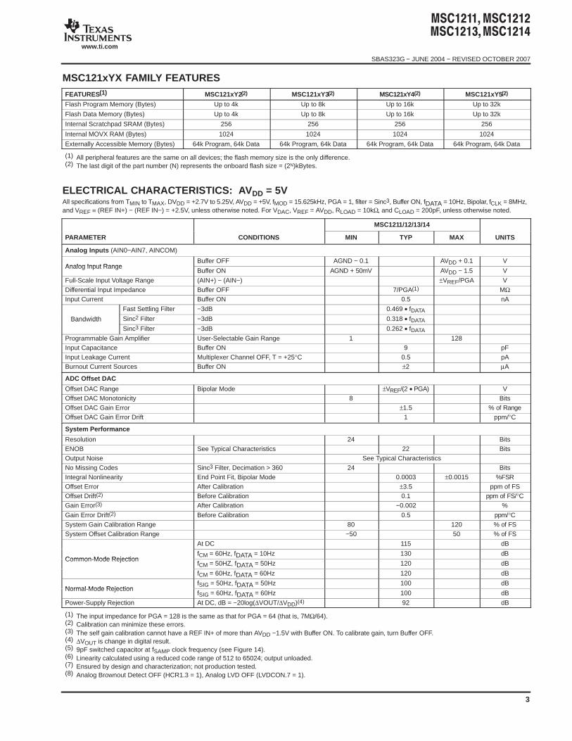
MSC121xYX FAMILY FEATURESFEATURES(1) MSC121xY2(2) MSC121xY3(2) MSC121xY4(2) MSC121xY5(2)
Flash Program Memory (Bytes) Up to 4k Up to 8k Up to 16k Up to 32k
Flash Data Memory (Bytes) Up to 4k Up to 8k Up to 16k Up to 32k
Internal Scratchpad SRAM (Bytes) 256 256 256 256
Internal MOVX RAM (Bytes) 1024 1024 1024 1024
Externally Accessible Memory (Bytes) 64k Program, 64k Data 64k Program, 64k Data 64k Program, 64k Data 64k Program, 64k Data
(1) All peripheral features are the same on all devices; the flash memory size is the only difference.(2) The last digit of the part number (N) represents the onboard flash size = (2N)kBytes.
ELECTRICAL CHARACTERISTICS: AV DD = 5V All specifications from TMIN to TMAX, DVDD = +2.7V to 5.25V, AVDD = +5V, fMOD = 15.625kHz, PGA = 1, filter = Sinc3, Buffer ON, fDATA = 10Hz, Bipolar, fCLK = 8MHz,and VREF ≡ (REF IN+) − (REF IN−) = +2.5V, unless otherwise noted. For VDAC, VREF = AVDD, RLOAD = 10kΩ, and CLOAD = 200pF, unless otherwise noted.
MSC1211/12/13/14
PARAMETER CONDITIONS MIN TYP MAX UNITS
Analog Inputs (AIN0−AIN7, AINCOM)
Analog Input RangeBuffer OFF AGND − 0.1 AVDD + 0.1 V
Analog Input RangeBuffer ON AGND + 50mV AVDD − 1.5 V
Full-Scale Input Voltage Range (AIN+) − (AIN−) ±VREF/PGA VDifferential Input Impedance Buffer OFF 7/PGA(1) MΩInput Current Buffer ON 0.5 nA
Fast Settling Filter −3dB 0.469 • fDATA
Bandwidth Sinc2 Filter −3dB 0.318 • fDATABandwidth
Sinc3 Filter −3dB 0.262 • fDATA
Programmable Gain Amplifier User-Selectable Gain Range 1 128Input Capacitance Buffer ON 9 pFInput Leakage Current Multiplexer Channel OFF, T = +25°C 0.5 pABurnout Current Sources Buffer ON ±2 µA
ADC Offset DAC
Offset DAC Range Bipolar Mode ±VREF/(2 • PGA) VOffset DAC Monotonicity 8 BitsOffset DAC Gain Error ±1.5 % of RangeOffset DAC Gain Error Drift 1 ppm/°C
System Performance
Resolution 24 BitsENOB See Typical Characteristics 22 BitsOutput Noise See Typical CharacteristicsNo Missing Codes Sinc3 Filter, Decimation > 360 24 BitsIntegral Nonlinearity End Point Fit, Bipolar Mode 0.0003 ±0.0015 %FSROffset Error After Calibration ±3.5 ppm of FSOffset Drift(2) Before Calibration 0.1 ppm of FS/°CGain Error(3) After Calibration −0.002 %
Gain Error Drift(2) Before Calibration 0.5 ppm/°CSystem Gain Calibration Range 80 120 % of FSSystem Offset Calibration Range −50 50 % of FS
At DC 115 dB
Common-Mode RejectionfCM = 60Hz, fDATA = 10Hz 130 dB
Common-Mode RejectionfCM = 50HZ, fDATA = 50Hz 120 dB
fCM = 60Hz, fDATA = 60Hz 120 dB
Normal-Mode RejectionfSIG = 50Hz, fDATA = 50Hz 100 dB
Normal-Mode RejectionfSIG = 60Hz, fDATA = 60Hz 100 dB
Power-Supply Rejection At DC, dB = −20log(∆VOUT/∆VDD)(4) 92 dB
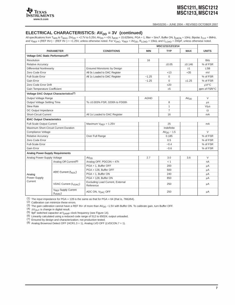
(1) The input impedance for PGA = 128 is the same as that for PGA = 64 (that is, 7MΩ/64).(2) Calibration can minimize these errors.(3) The self gain calibration cannot have a REF IN+ of more than AVDD −1.5V with Buffer ON. To calibrate gain, turn Buffer OFF.(4) ∆VOUT is change in digital result.(5) 9pF switched capacitor at fSAMP clock frequency (see Figure 14).(6) Linearity calculated using a reduced code range of 512 to 65024; output unloaded.(7) Ensured by design and characterization; not production tested.(8) Analog Brownout Detect OFF (HCR1.3 = 1), Analog LVD OFF (LVDCON.7 = 1).
SBAS323G − JUNE 2004 − REVISED OCTOBER 2007
www.ti.com
4
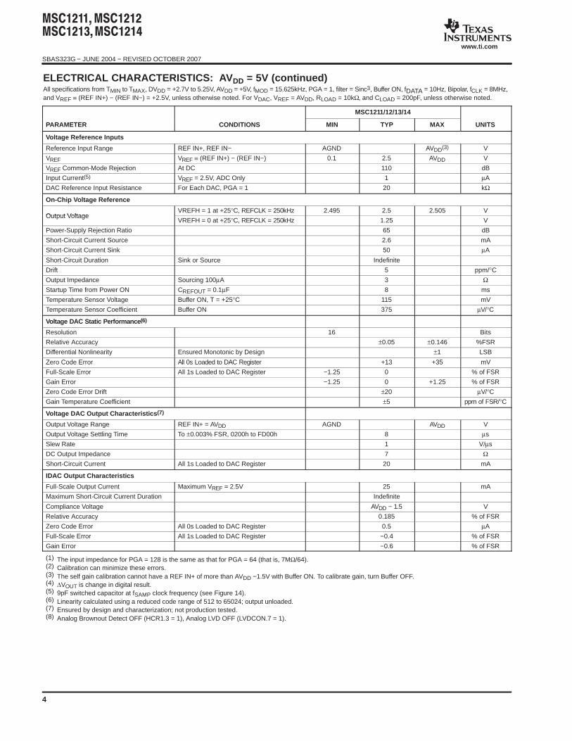
ELECTRICAL CHARACTERISTICS: AV DD = 5V (continued)All specifications from TMIN to TMAX, DVDD = +2.7V to 5.25V, AVDD = +5V, fMOD = 15.625kHz, PGA = 1, filter = Sinc3, Buffer ON, fDATA = 10Hz, Bipolar, fCLK = 8MHz,and VREF ≡ (REF IN+) − (REF IN−) = +2.5V, unless otherwise noted. For VDAC, VREF = AVDD, RLOAD = 10kΩ, and CLOAD = 200pF, unless otherwise noted.
MSC1211/12/13/14
PARAMETER UNITSMAXTYPMINCONDITIONS
Voltage Reference Inputs
Reference Input Range REF IN+, REF IN− AGND AVDD(3) V
VREF VREF ≡ (REF IN+) − (REF IN−) 0.1 2.5 AVDD V
VREF Common-Mode Rejection At DC 110 dB
Input Current(5) VREF = 2.5V, ADC Only 1 µA
DAC Reference Input Resistance For Each DAC, PGA = 1 20 kΩ
On-Chip Voltage Reference
Output VoltageVREFH = 1 at +25°C, REFCLK = 250kHz 2.495 2.5 2.505 V
Output VoltageVREFH = 0 at +25°C, REFCLK = 250kHz 1.25 V
Power-Supply Rejection Ratio 65 dB
Short-Circuit Current Source 2.6 mA
Short-Circuit Current Sink 50 µA
Short-Circuit Duration Sink or Source Indefinite
Drift 5 ppm/°C
Output Impedance Sourcing 100µA 3 ΩStartup Time from Power ON CREFOUT = 0.1µF 8 ms
Temperature Sensor Voltage Buffer ON, T = +25°C 115 mV
Temperature Sensor Coefficient Buffer ON 375 µV/°C
Voltage DAC Static Performance (6)
Resolution 16 Bits
Relative Accuracy ±0.05 ±0.146 %FSR
Differential Nonlinearity Ensured Monotonic by Design ±1 LSB
Zero Code Error All 0s Loaded to DAC Register +13 +35 mV
Full-Scale Error All 1s Loaded to DAC Register −1.25 0 % of FSR
Gain Error −1.25 0 +1.25 % of FSR
Zero Code Error Drift ±20 µV/°CGain Temperature Coefficient ±5 ppm of FSR/°C
Voltage DAC Output Characteristics (7)
Output Voltage Range REF IN+ = AVDD AGND AVDD V
Output Voltage Settling Time To ±0.003% FSR, 0200h to FD00h 8 µs
Slew Rate 1 V/µs
DC Output Impedance 7 ΩShort-Circuit Current All 1s Loaded to DAC Register 20 mA
IDAC Output Characteristics
Full-Scale Output Current Maximum VREF = 2.5V 25 mA
Maximum Short-Circuit Current Duration Indefinite
Compliance Voltage AVDD − 1.5 V
Relative Accuracy 0.185 % of FSR
Zero Code Error All 0s Loaded to DAC Register 0.5 µA
Full-Scale Error All 1s Loaded to DAC Register −0.4 % of FSR
Gain Error −0.6 % of FSR
(1) The input impedance for PGA = 128 is the same as that for PGA = 64 (that is, 7MΩ/64).(2) Calibration can minimize these errors.(3) The self gain calibration cannot have a REF IN+ of more than AVDD −1.5V with Buffer ON. To calibrate gain, turn Buffer OFF.(4) ∆VOUT is change in digital result.(5) 9pF switched capacitor at fSAMP clock frequency (see Figure 14).(6) Linearity calculated using a reduced code range of 512 to 65024; output unloaded.(7) Ensured by design and characterization; not production tested.(8) Analog Brownout Detect OFF (HCR1.3 = 1), Analog LVD OFF (LVDCON.7 = 1).
SBAS323G − JUNE 2004 − REVISED OCTOBER 2007
www.ti.com
5
ELECTRICAL CHARACTERISTICS: AV DD = 5V (continued)All specifications from TMIN to TMAX, DVDD = +2.7V to 5.25V, AVDD = +5V, fMOD = 15.625kHz, PGA = 1, filter = Sinc3, Buffer ON, fDATA = 10Hz, Bipolar, fCLK = 8MHz,and VREF ≡ (REF IN+) − (REF IN−) = +2.5V, unless otherwise noted. For VDAC, VREF = AVDD, RLOAD = 10kΩ, and CLOAD = 200pF, unless otherwise noted.
MSC1211/12/13/14
PARAMETER UNITSMAXTYPMINCONDITIONS
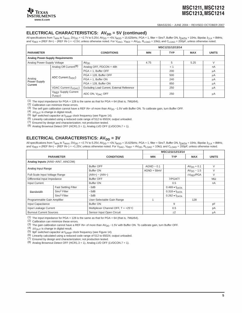
Analog Power-Supply Requirements
Analog Power-Supply Voltage AVDD 4.75 5 5.25 V
Analog Off Current(8) Analog OFF, PDCON = 48h < 1 nA
PGA = 1, Buffer OFF 200 µA
Analog ADC Current (IADC)PGA = 128, Buffer OFF 500 µA
AnalogPower-Supply
ADC Current (IADC)PGA = 1, Buffer ON 240 µA
Power-SupplyCurrent PGA = 128, Buffer ON 850 µACurrent
VDAC Current (IVDAC) Excluding Load Current, External Reference 250 µA
VREF Supply Current(IVREF)
ADC ON, VDAC OFF 250 µA
(1) The input impedance for PGA = 128 is the same as that for PGA = 64 (that is, 7MΩ/64).(2) Calibration can minimize these errors.(3) The self gain calibration cannot have a REF IN+ of more than AVDD −1.5V with Buffer ON. To calibrate gain, turn Buffer OFF.(4) ∆VOUT is change in digital result.(5) 9pF switched capacitor at fSAMP clock frequency (see Figure 14).(6) Linearity calculated using a reduced code range of 512 to 65024; output unloaded.(7) Ensured by design and characterization; not production tested.(8) Analog Brownout Detect OFF (HCR1.3 = 1), Analog LVD OFF (LVDCON.7 = 1).
ELECTRICAL CHARACTERISTICS: AV DD = 3V All specifications from TMIN to TMAX, DVDD = +2.7V to 5.25V, AVDD = +3V, fMOD = 15.625kHz, PGA = 1, filter = Sinc3, Buffer ON, fDATA = 10Hz, Bipolar, fCLK = 8MHz,and VREF ≡ (REF IN+) − (REF IN−) = +1.25V, unless otherwise noted. For VDAC, VREF = AVDD, RLOAD = 10kΩ, and CLOAD = 200pF, unless otherwise noted.
MSC1211/12/13/14
PARAMETER CONDITIONS MIN TYP MAX UNITS
Analog Inputs (AIN0−AIN7, AINCOM)
Analog Input RangeBuffer OFF AGND − 0.1 AVDD + 0.1 V
Analog Input RangeBuffer ON AGND + 50mV AVDD − 1.5 V
Full-Scale Input Voltage Range (AIN+) − (AIN−) ±VREF/PGA V
Differential Input Impedance Buffer OFF 7/PGA(1) MΩInput Current Buffer ON 0.5 nA
Fast Settling Filter −3dB 0.469 • fDATA
Bandwidth Sinc2 Filter −3dB 0.318 • fDATABandwidthSinc3 Filter −3dB 0.262 • fDATA
Programmable Gain Amplifier User-Selectable Gain Range 1 128
Input Capacitance Buffer ON 9 pF
Input Leakage Current Multiplexer Channel OFF, T = +25°C 0.5 pA
Burnout Current Sources Sensor Input Open Circuit ±2 µA
(1) The input impedance for PGA = 128 is the same as that for PGA = 64 (that is, 7MΩ/64).(2) Calibration can minimize these errors.(3) The gain calibration cannot have a REF IN+ of more than AVDD −1.5V with Buffer ON. To calibrate gain, turn Buffer OFF.(4) ∆VOUT is change in digital result.(5) 9pF switched capacitor at fSAMP clock frequency (see Figure 14).(6) Linearity calculated using a reduced code range of 512 to 65024; output unloaded.(7) Ensured by design and characterization; not production tested.(8) Analog Brownout Detect OFF (HCR1.3 = 1), Analog LVD OFF (LVDCON.7 = 1).
SBAS323G − JUNE 2004 − REVISED OCTOBER 2007
www.ti.com
6
ELECTRICAL CHARACTERISTICS: AV DD = 3V (continued)All specifications from TMIN to TMAX, DVDD = +2.7V to 5.25V, AVDD = +3V, fMOD = 15.625kHz, PGA = 1, filter = Sinc3, Buffer ON, fDATA = 10Hz, Bipolar, fCLK = 8MHz,and VREF ≡ (REF IN+) − (REF IN−) = +1.25V, unless otherwise noted. For VDAC, VREF = AVDD, RLOAD = 10kΩ, and CLOAD = 200pF, unless otherwise noted.
MSC1211/12/13/14
PARAMETER UNITSMAXTYPMINCONDITIONS
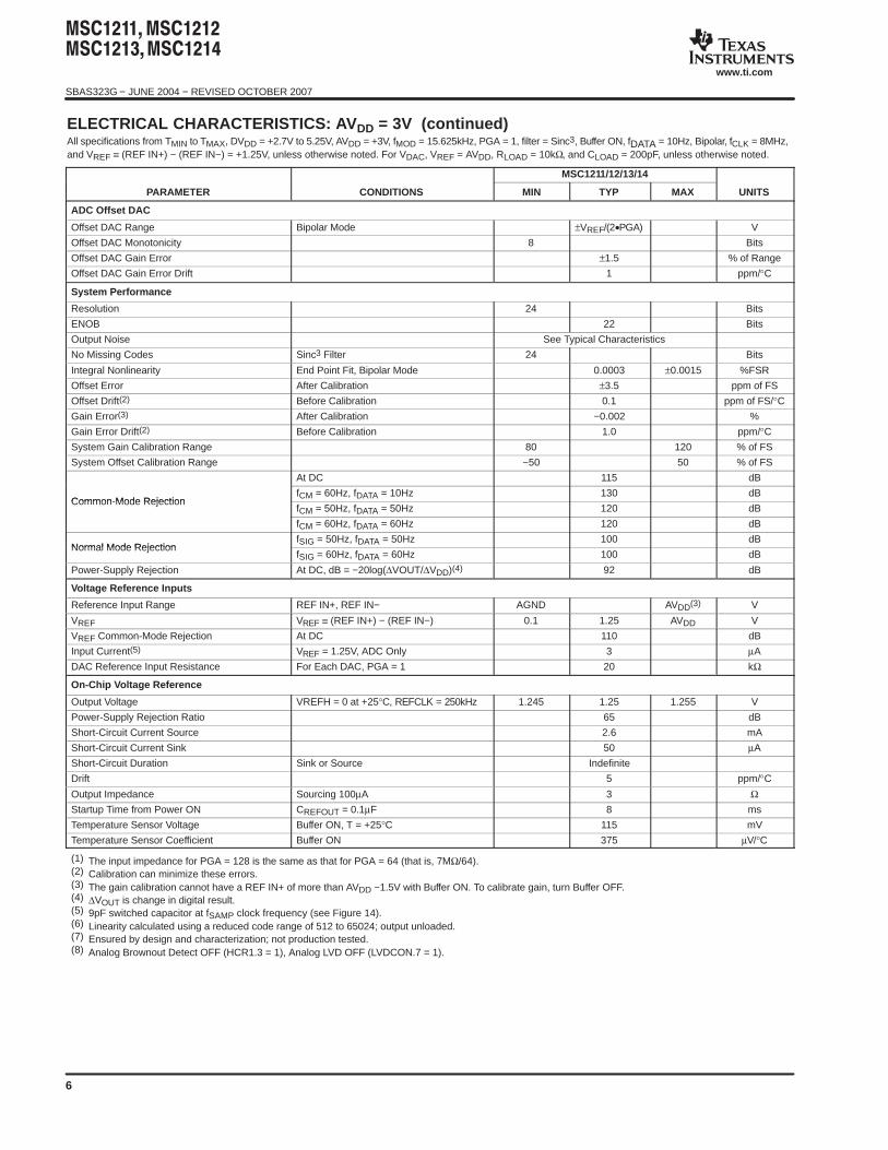
ADC Offset DAC
Offset DAC Range Bipolar Mode ±VREF/(2•PGA) V
Offset DAC Monotonicity 8 Bits
Offset DAC Gain Error ±1.5 % of Range
Offset DAC Gain Error Drift 1 ppm/°C
System Performance
Resolution 24 Bits
ENOB 22 Bits
Output Noise See Typical Characteristics
No Missing Codes Sinc3 Filter 24 Bits
Integral Nonlinearity End Point Fit, Bipolar Mode 0.0003 ±0.0015 %FSR
Offset Error After Calibration ±3.5 ppm of FS
Offset Drift(2) Before Calibration 0.1 ppm of FS/°C
Gain Error(3) After Calibration −0.002 %
Gain Error Drift(2) Before Calibration 1.0 ppm/°C
System Gain Calibration Range 80 120 % of FS
System Offset Calibration Range −50 50 % of FS
At DC 115 dB
Common-Mode RejectionfCM = 60Hz, fDATA = 10Hz 130 dB
Common-Mode RejectionfCM = 50Hz, fDATA = 50Hz 120 dB
fCM = 60Hz, fDATA = 60Hz 120 dB
Normal Mode RejectionfSIG = 50Hz, fDATA = 50Hz 100 dB
Normal Mode RejectionfSIG = 60Hz, fDATA = 60Hz 100 dB
Power-Supply Rejection At DC, dB = −20log(∆VOUT/∆VDD)(4) 92 dB
Voltage Reference Inputs
Reference Input Range REF IN+, REF IN− AGND AVDD(3) V
VREF VREF ≡ (REF IN+) − (REF IN−) 0.1 1.25 AVDD V
VREF Common-Mode Rejection At DC 110 dB
Input Current(5) VREF = 1.25V, ADC Only 3 µA
DAC Reference Input Resistance For Each DAC, PGA = 1 20 kΩ
On-Chip Voltage Reference
Output Voltage VREFH = 0 at +25°C, REFCLK = 250kHz 1.245 1.25 1.255 V
Power-Supply Rejection Ratio 65 dB
Short-Circuit Current Source 2.6 mA
Short-Circuit Current Sink 50 µA
Short-Circuit Duration Sink or Source Indefinite
Drift 5 ppm/°C
Output Impedance Sourcing 100µA 3 ΩStartup Time from Power ON CREFOUT = 0.1µF 8 ms
Temperature Sensor Voltage Buffer ON, T = +25°C 115 mV
Temperature Sensor Coefficient Buffer ON 375 µV/°C
(1) The input impedance for PGA = 128 is the same as that for PGA = 64 (that is, 7MΩ/64).(2) Calibration can minimize these errors.(3) The gain calibration cannot have a REF IN+ of more than AVDD −1.5V with Buffer ON. To calibrate gain, turn Buffer OFF.(4) ∆VOUT is change in digital result.(5) 9pF switched capacitor at fSAMP clock frequency (see Figure 14).(6) Linearity calculated using a reduced code range of 512 to 65024; output unloaded.(7) Ensured by design and characterization; not production tested.(8) Analog Brownout Detect OFF (HCR1.3 = 1), Analog LVD OFF (LVDCON.7 = 1).
SBAS323G − JUNE 2004 − REVISED OCTOBER 2007
www.ti.com
7
ELECTRICAL CHARACTERISTICS: AV DD = 3V (continued)All specifications from TMIN to TMAX, DVDD = +2.7V to 5.25V, AVDD = +3V, fMOD = 15.625kHz, PGA = 1, filter = Sinc3, Buffer ON, fDATA = 10Hz, Bipolar, fCLK = 8MHz,and VREF ≡ (REF IN+) − (REF IN−) = +1.25V, unless otherwise noted. For VDAC, VREF = AVDD, RLOAD = 10kΩ, and CLOAD = 200pF, unless otherwise noted.
MSC1211/12/13/14
PARAMETER UNITSMAXTYPMINCONDITIONS
Voltage DAC Static Performance (6)
Resolution 16 Bits
Relative Accuracy ±0.05 ±0.146 % of FSR
Differential Nonlinearity Ensured Monotonic by Design ±1 LSB
Zero Code Error All 0s Loaded to DAC Register +13 +35 mV
Full-Scale Error All 1s Loaded to DAC Register −1.25 0 % of FSR
Gain Error −1.25 0 ±1.25 % of FSR
Zero Code Error Drift ±20 µV/°CGain Temperature Coefficient ±5 ppm of FSR/°C
Voltage DAC Output Characteristics (7)
Output Voltage Range AGND AVDD V
Output Voltage Settling Time To ±0.003% FSR, 0200h to FD00h 8 µs
Slew Rate 1 V/µs
DC Output Impedance 7 ΩShort-Circuit Current All 1s Loaded to DAC Register 16 mA
IDAC Output Characteristics
Full-Scale Output Current Maximum VREF = 1.25V 25 mA
Maximum Short-Circuit Current Duration Indefinite
Compliance Voltage AVDD − 1.5 V
Relative Accuracy Over Full Range 0.185 % of FSR
Zero Code Error 0.5 % of FSR
Full-Scale Error −0.4 % of FSR
Gain Error −0.6 % of FSR
Analog Power-Supply Requirements
Analog Power-Supply Voltage AVDD 2.7 3.0 3.6 V
Analog Off Current(8) Analog OFF, PDCON = 47h < 1 nA
PGA = 1, Buffer OFF 200 µA
ADC Current (IADC)PGA = 128, Buffer OFF 500 µA
AnalogADC Current (IADC)
PGA = 1, Buffer ON 240 µAAnalogPower-SupplyCurrent
PGA = 128, Buffer ON 850 µAPower-SupplyCurrent
VDAC Current (IVDAC)Excluding Load Current, ExternalReference
250 µA
VREF Supply Current(IVDAC)
ADC ON, VDAC OFF 250 µA
(1) The input impedance for PGA = 128 is the same as that for PGA = 64 (that is, 7MΩ/64).(2) Calibration can minimize these errors.(3) The gain calibration cannot have a REF IN+ of more than AVDD −1.5V with Buffer ON. To calibrate gain, turn Buffer OFF.(4) ∆VOUT is change in digital result.(5) 9pF switched capacitor at fSAMP clock frequency (see Figure 14).(6) Linearity calculated using a reduced code range of 512 to 65024; output unloaded.(7) Ensured by design and characterization; not production tested.(8) Analog Brownout Detect OFF (HCR1.3 = 1), Analog LVD OFF (LVDCON.7 = 1).
SBAS323G − JUNE 2004 − REVISED OCTOBER 2007
www.ti.com
8
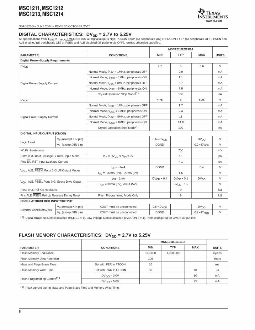
DIGITAL CHARACTERISTICS: DV DD = 2.7V to 5.25VAll specifications from TMIN to TMAX, FMCON = 10h, all digital outputs high, PDCON = 00h (all peripherals ON) or PDCON = FFh (all peripherals OFF), PSEN andALE enabled (all peripherals ON) or PSEN and ALE disabled (all peripherals OFF), unless otherwise specified.
MSC1211/12/13/14
PARAMETER CONDITIONS MIN TYP MAX UNITS
Digital Power-Supply Requirements
DVDD 2.7 3 3.6 V
Normal Mode, fOSC = 1MHz, peripherals OFF 0.9 mA
Normal Mode, fOSC = 1MHz, peripherals ON 1.1 mA
Digital Power-Supply Current Normal Mode, fOSC = 8MHz, peripherals OFF 5.7 mADigital Power-Supply Current
Normal Mode, fOSC = 8MHz, peripherals ON 7.5 mA
Crystal Operation Stop Mode(1) 100 nA
DVDD 4.75 5 5.25 V
Normal Mode, fOSC = 1MHz, peripherals OFF 1.7 mA
Normal Mode, fOSC = 1MHz, peripherals ON 2.4 mA
Digital Power-Supply Current Normal Mode, fOSC = 8MHz, peripherals OFF 11 mADigital Power-Supply Current
Normal Mode, fOSC = 8MHz, peripherals ON 14.8 mA
Crystal Operation Stop Mode(1) 100 nA
DIGITAL INPUT/OUTPUT (CMOS)
Logic LevelVIH (except XIN pin) 0.6 • DVDD DVDD V
Logic LevelVIL (except XIN pin) DGND 0.2 • DVDD V
I/O Pin Hysteresis 700 mV
Ports 0−3, Input Leakage Current, Input Mode VIH = DVDD or VIH = 0V < 1 pA
Pins EA, RST Input Leakage Current < 1 pA
VOL, ALE, PSEN, Ports 0−3, All Output ModesIOL = −1mA DGND 0.4 V
VOL, ALE, PSEN, Ports 0−3, All Output ModesIOL = −30mA (5V), −20mA (3V) 1.5 V
VOH, ALE, PSEN, Ports 0−3, Strong Drive OutputIOH = 1mA DVDD − 0.4 DVDD − 0.1 DVDD V
VOH, ALE, PSEN, Ports 0−3, Strong Drive OutputIOH = 30mA (5V), 20mA (5V) DVDD − 1.5 V
Ports 0−3, Pull-Up Resistors 9 kΩ
Pins ALE, PSEN, Pull-Up Resistors During Reset Flash Programming Mode Only 9 kΩ
OSCILLATOR/CLOCK INPUT/OUTPUT
External Oscillator/ClockVIH (except XIN pin) XOUT must be unconnected 0.6 • DVDD DVDD V
External Oscillator/ClockVIL (except XIN pin) XOUT must be unconnected DGND 0.2 • DVDD V
(1) Digital Brownout Detect disabled (HCR1.2 = 1), Low Voltage Detect disabled (LVDCON.3 = 1). Ports configured for CMOS output low.
FLASH MEMORY CHARACTERISTICS: DV DD = 2.7V to 5.25VMSC1211/12/13/14
PARAMETER CONDITIONS MIN TYP MAX UNITS
Flash Memory Endurance 100,000 1,000,000 Cycles
Flash Memory Data Retention 100 Years
Mass and Page Erase Time Set with FER in FTCON 10 ms
Flash Memory Write Time Set with FWR in FTCON 30 40 µs
Flash Programming Current(1)DVDD = 3.0V 10 mA
Flash Programming Current(1)DVDD = 5.0V 25 mA
(1) Peak current during Mass and Page Erase Time and Memory Write Time.
SBAS323G − JUNE 2004 − REVISED OCTOBER 2007
www.ti.com
9
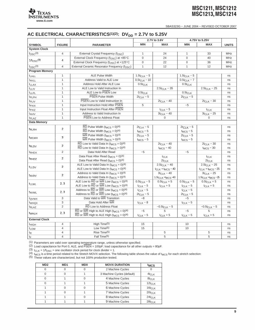
AC ELECTRICAL CHARACTERISTICS (1)(2): DVDD = 2.7V to 5.25V2.7V to 3.6V 4.75V to 5.25V
SYMBOL FIGURE PARAMETER MIN MAX MIN MAX UNITSSystem Clock
fOSC(3) 4 External Crystal Frequency (fOSC) 1 24 1 33 MHz
1/tOSC(3) 4External Clock Frequency (fOSC) at +85°C 0 24 0 40 MHz
1/tOSC(3) 4External Clock Frequency (fOSC) at +125°C 0 22 0 36 MHz
fOSC(3) 4 External Ceramic Resonator Frequency (fOSC) 1 12 1 12 MHz
Program Memory
tLHLL 1 ALE Pulse Width 1.5tCLK − 5 1.5tCLK − 5 ns
tAVLL 1 Address Valid to ALE Low 0.5tCLK − 10 0.5tCLK − 7 nstLLAX 1 Address Hold After ALE Low 0.5tCLK 0.5tCLK nstLLIV 1 ALE Low to Valid Instruction In 2.5tCLK − 35 2.5tCLK − 25 nstLLPL 1 ALE Low to PSEN Low 0.5tCLK 0.5tCLK nstPLPH 1 PSEN Pulse Width 2tCLK − 5 2tCLK − 5 nstPLIV 1 PSEN Low to Valid Instruction In 2tCLK − 40 2tCLK − 30 nstPXIX 1 Input Instruction Hold After PSEN 5 −5 nstPXIZ 1 Input Instruction Float After PSEN tCLK − 5 tCLK nstAVIV 1 Address to Valid Instruction In 3tCLK − 40 3tCLK − 25 nstPLAZ 1 PSEN Low to Address Float 0 0 ns
Data Memory
tRLRH 2RD Pulse Width (tMCS = 0)(4) 2tCLK − 5 2tCLK − 5 ns
tRLRH 2RD Pulse Width (tMCS > 0)(4) tMCS − 5 tMCS − 5 ns
tWLWH 3WR Pulse Width (tMCS = 0)(4) 2tCLK − 5 2tCLK − 5 ns
tWLWH 3WR Pulse Width (tMCS > 0)(4) tMCS − 5 tMCS − 5 ns
tRLDV 2RD Low to Valid Data In (tMCS = 0)(4) 2tCLK − 40 2tCLK − 30 ns
tRLDV 2RD Low to Valid Data In (tMCS > 0)(4) tMCS − 40 tMCS − 30 ns
tRHDX 2 Data Hold After Read −5 −5 ns
tRHDZ 2Data Float After Read (tMCS = 0)(4) tCLK tCLK ns
tRHDZ 2Data Float After Read (tMCS > 0)(4) 2tCLK 2tCLK ns
tLLDV 2ALE Low to Valid Data In (tMCS = 0)(4) 2.5tCLK − 40 2.5tCLK − 25 ns
tLLDV 2ALE Low to Valid Data In (tMCS > 0)(4) tCLK + tMCS − 40 tCLK + tMCS − 25 ns
tAVDV 2Address to Valid Data In (tMCS = 0)(4) 3tCLK − 40 3tCLK − 25 ns
tAVDV 2Address to Valid Data In (tMCS > 0)(4) 1.5tCLK + tMCS −40 1.5tCLK + tMCS − 25 ns
tLLWL 2, 3ALE Low to RD or WR Low (tMCS = 0)(4) 0.5tCLK − 5 0.5tCLK + 5 0.5tCLK − 5 0.5tCLK + 5 ns
tLLWL 2, 3ALE Low to RD or WR Low (tMCS > 0)(4) tCLK − 5 tCLK + 5 tCLK − 5 tCLK + 5 ns
tAVWL 2, 3Address to RD or WR Low (tMCS = 0)(4) tCLK − 5 tCLK − 5 ns
tAVWL 2, 3Address to RD or WR Low (tMCS > 0)(4) 2tCLK − 5 2tCLK − 5 ns
tQVWX 3 Data Valid to WR Transition −8 −5 nstWHQX 3 Data Hold After WR tCLK − 8 tCLK − 5 nstRLAZ 2 RD Low to Address Float −0.5tCLK − 5 −0.5tCLK − 5 ns
tWHLH 2, 3RD or WR High to ALE High (tMCS = 0)(4) −5 5 −5 5 ns
tWHLH 2, 3RD or WR High to ALE High (tMCS > 0)(4) tCLK − 5 tCLK + 5 tCLK − 5 tCLK + 5 ns
External Clock
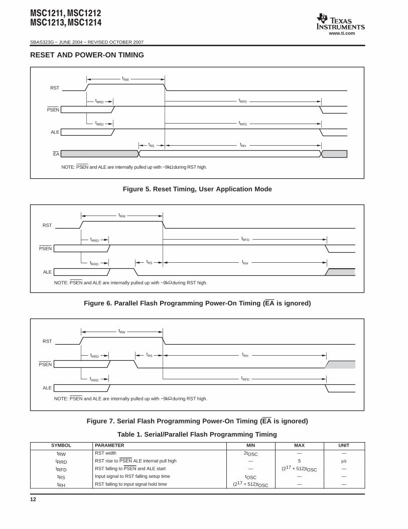
tHIGH 4 High Time(5) 15 10 nstLOW 4 Low Time(5) 15 10 nstR 4 Rise Time(5) 5 5 nstF 4 Fall Time(5) 5 5 ns
(1) Parameters are valid over operating temperature range, unless otherwise specified.(2) Load capacitance for Port 0, ALE, and PSEN = 100pF; load capacitance for all other outputs = 80pF.(3) tCLK = 1/fOSC = one oscillator clock period for clock divider = 1.(4) tMCS is a time period related to the Stretch MOVX selection. The following table shows the value of tMCS for each stretch selection:(5) These values are characterized, but not 100% production tested.
MD2 MD1 MD0 MOVX DURATION tMCS0 0 0 2 Machine Cycles 0
0 0 1 3 Machine Cycles (default) 4tCLK
0 1 0 4 Machine Cycles 8tCLK
0 1 1 5 Machine Cycles 12tCLK
1 0 0 6 Machine Cycles 16tCLK
1 0 1 7 Machine Cycles 20tCLK
1 1 0 8 Machine Cycles 24tCLK
1 1 1 9 Machine Cycles 28tCLK
SBAS323G − JUNE 2004 − REVISED OCTOBER 2007
www.ti.com
10
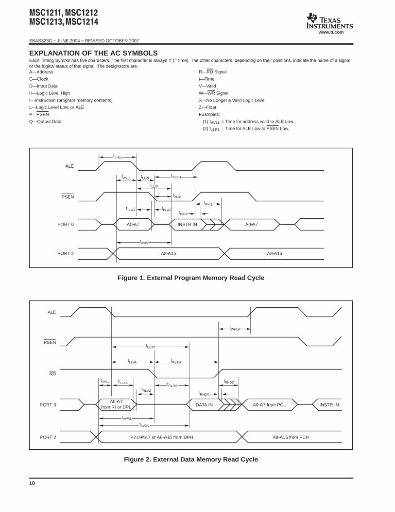
EXPLANATION OF THE AC SYMBOLSEach Timing Symbol has five characters. The first character is always ’t’ (= time). The other characters, depending on their positions, indicate the name of a signalor the logical status of that signal. The designators are:AAddress
CClock
DInput Data
HLogic Level High
IInstruction (program memory contents)
LLogic Level Low, or ALE
PPSEN
QOutput Data
RRD Signal
tTime
VValid
WWR Signal
XNo Longer a Valid Logic Level
ZFloat
Examples:
(1) tAVLL = Time for address valid to ALE Low.
(2) tLLPL = Time for ALE Low to PSEN Low.
tLHLL
tAVLL tLLPLtPLPH
tLLIV
tLLAX tPLAZ
tPXIZ
tPXIX
tAVIV
tPLIV
A0−A7 A0−A7
A8−A15A8−A15
INSTR IN
ALE
PSEN
PORT 0
PORT 2
Figure 1. External Program Memory Read Cycle
tAVLL
ALE
RD
PSEN
PORT 0
PORT 2
A0−A7from RI or DPL DATA IN A0−A7 from PCL INSTR IN
P2.0−P2.7 or A8−A15 from DPH A8−A15 from PCH
tAVDV
tLLDV
tWHLH
tRLRHtLLWL
tLLAX
tRLAZ tRHDX
tRLDV
tAVWL
tRHDZ
Figure 2. External Data Memory Read Cycle
SBAS323G − JUNE 2004 − REVISED OCTOBER 2007
www.ti.com
11
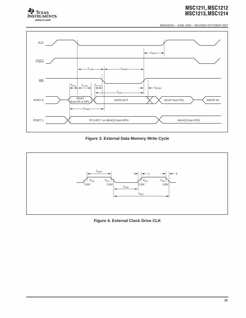
tWHLH
tAVLL
tLLWL
tWHQX
tLLAX
tAVWL
tWLWH
tDW
tQVWX
ALE
WR
PSEN
PORT 0
PORT 2
A0−A7from RI or DPL DATA OUT A0−A7 from PCL INSTR IN
P2.0−P2.7 or A8−A15 from DPH A8−A15 from PCH
Figure 3. External Data Memory Write Cycle
trtHIGH
VIH1 VIH1
0.8V 0.8V
VIH1 VIH1
0.8V 0.8VtLOW
tOSC
tf
Figure 4. External Clock Drive CLK
SBAS323G − JUNE 2004 − REVISED OCTOBER 2007
www.ti.com
12
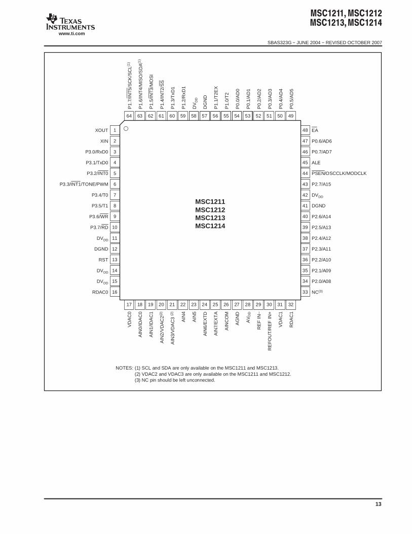
RESET AND POWER-ON TIMING
tRW
tRS tRH
tRFD
tRFD
RST
PSEN
ALE
NOTE: PSEN and ALE are internally pulled up with ~9kΩduring RST high.
EA
tRRD
tRRD
Figure 5. Reset Timing, User Application Mode
tRFD
PSEN
ALE
NOTE: PSEN and ALE are internally pulled up with ~9kΩduring RST high.
tRW
RST
tRS tRH
tRRD
tRRD
Figure 6. Parallel Flash Programming Power-On Timing (EA is ignored)
tRFD
PSEN
ALE
NOTE: PSEN and ALE are internally pulled up with ~9kΩduring RST high.
tRW
RST
tRS tRHtRRD
tRRD
Figure 7. Serial Flash Programming Power-On Timing (EA is ignored)
Table 1. Serial/Parallel Flash Programming Timing
SYMBOL PARAMETER MIN MAX UNIT
tRW RST width 2tOSC — —
tRRD RST rise to PSEN ALE internal pull high — 5 µs
tRFD RST falling to PSEN and ALE start — (217 + 512)tOSC —
tRS Input signal to RST falling setup time tOSC — —
tRH RST falling to input signal hold time (217 + 512)tOSC — —
SBAS323G − JUNE 2004 − REVISED OCTOBER 2007
www.ti.com
13
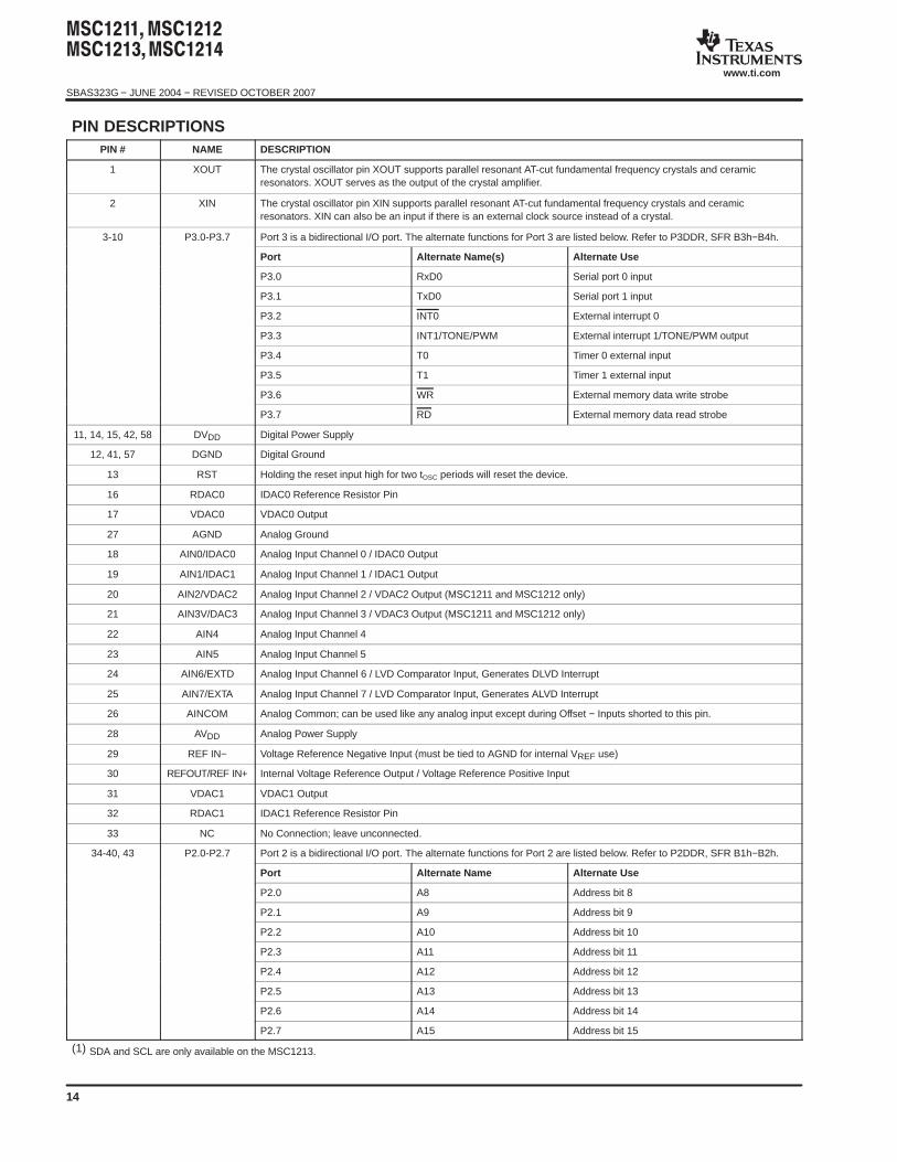
48
47
46
45
44
43
42
41
40
39
38
37
36
35
34
33
EA
P0.6/AD6
P0.7/AD7
ALE
PSEN/OSCCLK/MODCLK
P2.7/A15
DVDD
DGND
P2.6/A14
P2.5/A13
P2.4/A12
P2.3/A11
P2.2/A10
P2.1/A09
P2.0/A08
NC(3)
1
2
3
4
5
6
7
8
9
10
11
12
13
14
15
16
XOUT
XIN
P3.0/RxD0
P3.1/TxD0
P3.2/INT0
P3.3/INT1/TONE/PWM
P3.4/T0
P3.5/T1
P3.6/WR
P3.7/RD
DVDD
DGND
RST
DVDD
DVDD
RDAC0
P1.
7/IN
T5/
SC
K/S
CL(1
)
P1.
6/IN
T4/
MIS
O/S
DA
(1)
P1.
5/IN
T3/
MO
SI
P1.
4/IN
T2/
SS
P1.
3/T
xD1
P1.
2/R
xD1
DV
DD
DG
ND
P1.
1/T
2EX
P1.
0/T
2
P0.
0/A
D0
P0.
1/A
D1
P0.
2/A
D2
P0.
3/A
D3
P0.
4/A
D4
P0.
5/A
D5
VD
AC
0
AIN
0/ID
AC
0
AIN
1/ID
AC
1
AIN
2/V
DA
C2
(2)
AIN
3/V
DA
C3
(2)
AIN
4
AIN
5
AIN
6/E
XT
D
AIN
7/E
XT
A
AIN
CO
M
AG
ND
AV
DD
RE
FIN
−
RE
FO
UT
/RE
FIN
+
VD
AC
1
RD
AC
1
64 63 62 61 60 59 58 57 56 55 54
17 18 19 20 21 22 23 24 25 26 27
53 52 51 50 49
28 29 30 31 32
MSC1211MSC1212MSC1213MSC1214
(1) SCL and SDA are only available on the MSC1211 and MSC1213.(2) VDAC2 and VDAC3 are only available on the MSC1211 and MSC1212.(3) NC pin should be left unconnected.
NOTES:
SBAS323G − JUNE 2004 − REVISED OCTOBER 2007
www.ti.com
14
PIN DESCRIPTIONS PIN # NAME DESCRIPTION
1 XOUT The crystal oscillator pin XOUT supports parallel resonant AT-cut fundamental frequency crystals and ceramicresonators. XOUT serves as the output of the crystal amplifier.
2 XIN The crystal oscillator pin XIN supports parallel resonant AT-cut fundamental frequency crystals and ceramicresonators. XIN can also be an input if there is an external clock source instead of a crystal.
3-10 P3.0-P3.7 Port 3 is a bidirectional I/O port. The alternate functions for Port 3 are listed below. Refer to P3DDR, SFR B3h−B4h.3-10 P3.0-P3.7
Port Alternate Name(s) Alternate Use
P3.0 RxD0 Serial port 0 input
P3.1 TxD0 Serial port 1 input
P3.2 INT0 External interrupt 0
P3.3 INT1/TONE/PWM External interrupt 1/TONE/PWM output
P3.4 T0 Timer 0 external input
P3.5 T1 Timer 1 external input
P3.6 WR External memory data write strobe
P3.7 RD External memory data read strobe
11, 14, 15, 42, 58 DVDD Digital Power Supply
12, 41, 57 DGND Digital Ground
13 RST Holding the reset input high for two tOSC periods will reset the device.
16 RDAC0 IDAC0 Reference Resistor Pin
17 VDAC0 VDAC0 Output
27 AGND Analog Ground
18 AIN0/IDAC0 Analog Input Channel 0 / IDAC0 Output
19 AIN1/IDAC1 Analog Input Channel 1 / IDAC1 Output
20 AIN2/VDAC2 Analog Input Channel 2 / VDAC2 Output (MSC1211 and MSC1212 only)
21 AIN3V/DAC3 Analog Input Channel 3 / VDAC3 Output (MSC1211 and MSC1212 only)
22 AIN4 Analog Input Channel 4
23 AIN5 Analog Input Channel 5
24 AIN6/EXTD Analog Input Channel 6 / LVD Comparator Input, Generates DLVD Interrupt
25 AIN7/EXTA Analog Input Channel 7 / LVD Comparator Input, Generates ALVD Interrupt
26 AINCOM Analog Common; can be used like any analog input except during Offset − Inputs shorted to this pin.
28 AVDD Analog Power Supply
29 REF IN− Voltage Reference Negative Input (must be tied to AGND for internal VREF use)
30 REFOUT/REF IN+ Internal Voltage Reference Output / Voltage Reference Positive Input
31 VDAC1 VDAC1 Output
32 RDAC1 IDAC1 Reference Resistor Pin
33 NC No Connection; leave unconnected.
34-40, 43 P2.0-P2.7 Port 2 is a bidirectional I/O port. The alternate functions for Port 2 are listed below. Refer to P2DDR, SFR B1h−B2h.34-40, 43 P2.0-P2.7
Port Alternate Name Alternate Use
P2.0 A8 Address bit 8
P2.1 A9 Address bit 9
P2.2 A10 Address bit 10
P2.3 A11 Address bit 11
P2.4 A12 Address bit 12
P2.5 A13 Address bit 13
P2.6 A14 Address bit 14
P2.7 A15 Address bit 15
(1) SDA and SCL are only available on the MSC1213.
SBAS323G − JUNE 2004 − REVISED OCTOBER 2007
www.ti.com
15
PIN DESCRIPTIONS (continued)PIN # DESCRIPTIONNAME
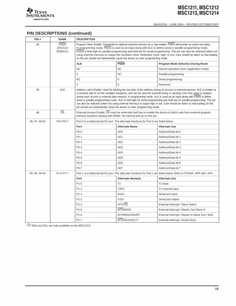
44 PSENOSCCLKMODCLK
Program Store Enable: Connected to optional external memory as a chip enable. PSEN will provide an active low pulse.In programming mode, PSEN is used as an input along with ALE to define serial or parallel programming mode.PSEN is held high for parallel programming and held low for serial programming. This pin can also be selected (when notusing external memory) to output the Oscillator clock, Modulator clock, high, or low. Care should be taken so that loadingon this pin should not inadvertently cause the device to enter programming mode.
ALE PSEN Program Mode Selection During Reset
NC NC Normal operation (User Application mode)
0 NC Parallel programming
NC 0 Serial programming
0 0 Reserved
45 ALE Address Latch Enable: Used for latching the low byte of the address during an access to external memory. ALE is emitted ata constant rate of 1/4 the oscillator frequency, and can be used for external timing or clocking. One ALE pulse is skippedduring each access to external data memory. In programming mode, ALE is used as an input along with PSEN to defineserial or parallel programming mode. ALE is held high for serial programming and held low for parallel programming. This pincan also be selected (when not using external memory) to output high or low. Care should be taken so that loading on thispin should not inadvertently cause the device to enter programming mode.
48 EA External Access Enable: EA must be externally held low to enable the device to fetch code from external programmemory locations starting with 0000h. No internal pull-up on this pin.
46, 47, 49-54 P0.0-P0.7 Port 0 is a bidirectional I/O port. The alternate functions for Port 0 are listed below.46, 47, 49-54 P0.0-P0.7
Port Alternate Name Alternate Use
P0.0 AD0 Address/Data bit 0
P0.1 AD1 Address/Data bit 1
P0.2 AD2 Address/Data bit 2
P0.3 AD3 Address/Data bit 3
P0.4 AD4 Address/Data bit 4
P0.5 AD5 Address/Data bit 5
P0.6 AD6 Address/Data bit 6
P0.7 AD7 Address/Data bit 7
55, 56, 59-64
P1.0-P1.7 Port 1 is a bidirectional I/O port. The alternate functions for Port 1 are listed below. Refer to P1DDR, SFR AEh−AFh.55, 56, 59-64
P1.0-P1.7
Port Alternate Name(s) Alternate Use
P1.0 T2 T2 input
P1.1 T2EX T2 external input
P1.2 RxD1 Serial port input
P1.3 TxD1 Serial port output
P1.4 INT2/SS External Interrupt / Slave Select
P1.5 INT3/MOSI External Interrupt / Master Out-Slave In
P1.6 INT4/MISO/SDA(1) External Interrupt / Master In-Slave Out / SDA
P1.7 INT5/SCK/SCL(1) External Interrupt / Serial Clock
(1) SDA and SCL are only available on the MSC1213.
SBAS323G − JUNE 2004 − REVISED OCTOBER 2007
www.ti.com
16
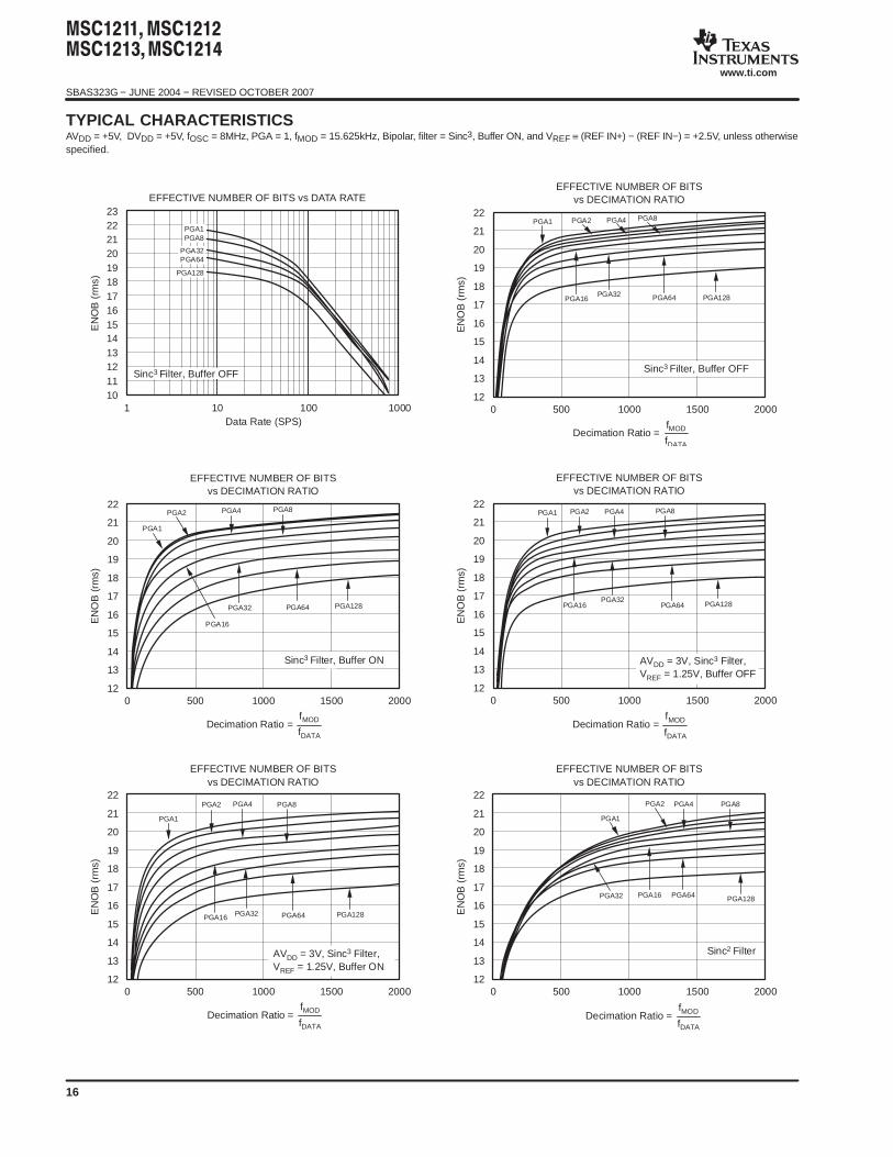
TYPICAL CHARACTERISTICSAVDD = +5V, DVDD = +5V, fOSC = 8MHz, PGA = 1, fMOD = 15.625kHz, Bipolar, filter = Sinc3, Buffer ON, and VREF ≡ (REF IN+) − (REF IN−) = +2.5V, unless otherwisespecified.
EFFECTIVE NUMBER OF BITS vs DATA RATE2322212019181716151413121110
EN
OB
(rm
s)
Data Rate (SPS)1 10 100 1000
Sinc3 Filter, Buffer OFF
PGA1PGA8
PGA32PGA64
PGA128
22
21
20
19
18
17
16
15
14
13
12
EFFECTIVE NUMBER OF BITSvs DECIMATION RATIO
Decimation Ratio =fMOD
fDATA
0 500 1000 1500 2000
PGA4
EN
OB
(rm
s)
PGA1 PGA2
PGA16
PGA8
PGA32 PGA64 PGA128
Sinc3 Filter, Buffer OFF
22
21
20
19
18
17
16
15
14
13
12
EFFECTIVE NUMBER OF BITSvs DECIMATION RATIO
0 500 1000 1500 2000
EN
OB
(rm
s)
PGA4 PGA8
PGA1
PGA2
PGA16
PGA32 PGA64 PGA128
Decimation Ratio =fMOD
fDATA
Sinc3 Filter, Buffer ON
22
21
20
19
18
17
16
15
14
13
12
EFFECTIVE NUMBER OF BITSvs DECIMATION RATIO
0 500 1000 1500 2000
EN
OB
(rm
s)
PGA4 PGA8PGA1 PGA2
PGA16PGA32
PGA64 PGA128
Decimation Ratio =fMOD
fDATA
AVDD = 3V, Sinc3 Filter,VREF = 1.25V, Buffer OFF
22
21
20
19
18
17
16
15
14
13
12
EFFECTIVE NUMBER OF BITSvs DECIMATION RATIO
0 500 1000 1500 2000
EN
OB
(rm
s)
PGA4 PGA8
PGA1
PGA2
PGA16 PGA32 PGA64 PGA128
AVDD = 3V, Sinc3 Filter,VREF = 1.25V, Buffer ON
Decimation Ratio =fMOD
fDATA
22
21
20
19
18
17
16
15
14
13
12
EFFECTIVE NUMBER OF BITSvs DECIMATION RATIO
0 500 1000 1500 2000
EN
OB
(rm
s)
PGA4 PGA8
PGA1
PGA2
PGA32 PGA128PGA16 PGA64
Decimation Ratio =fMOD
fDATA
Sinc2 Filter
SBAS323G − JUNE 2004 − REVISED OCTOBER 2007
www.ti.com
17
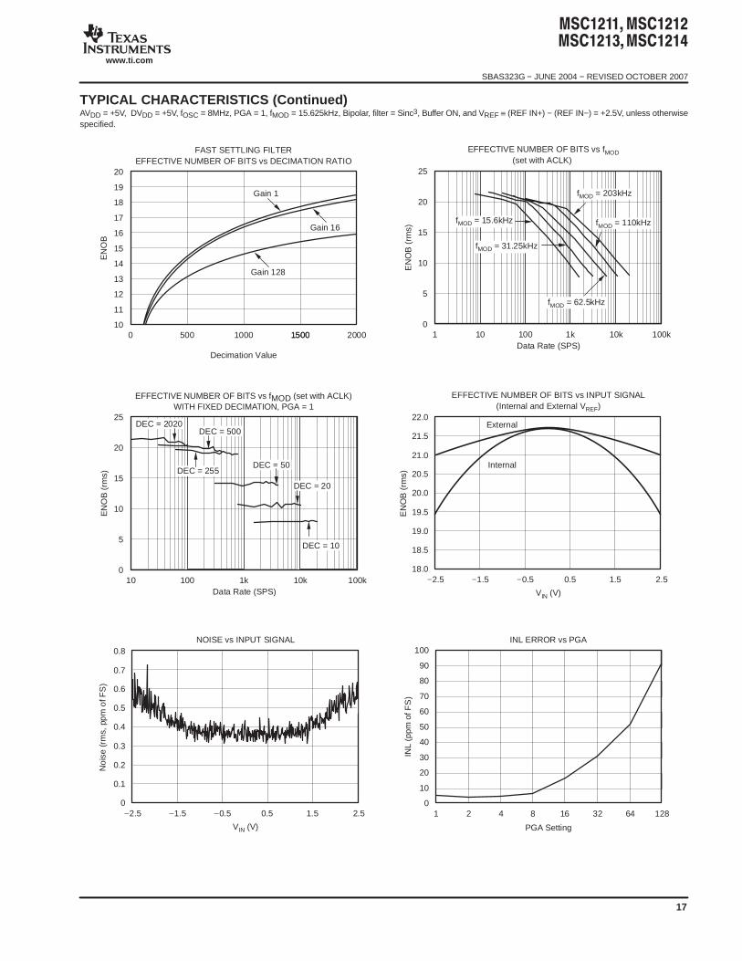
TYPICAL CHARACTERISTICS (Continued)AVDD = +5V, DVDD = +5V, fOSC = 8MHz, PGA = 1, fMOD = 15.625kHz, Bipolar, filter = Sinc3, Buffer ON, and VREF ≡ (REF IN+) − (REF IN−) = +2.5V, unless otherwisespecified.
20
19
18
17
16
15
14
13
12
11
10
FAST SETTLING FILTEREFFECTIVE NUMBER OF BITS vs DECIMATION RATIO
0 500 1000
Gain 1
Gain 16
Gain 128
1500 2000
EN
OB
1500
Decimation Value
EFFECTIVE NUMBER OF BITS vs fMOD(set with ACLK)
25
20
15
10
5
0
EN
OB
(rm
s)
Data Rate (SPS)1 10 100 1k 10k 100k
fMOD = 15.6kHz
fMOD = 62.5kHz
fMOD = 203kHz
fMOD = 110kHz
fMOD = 31.25kHz
25
20
15
10
5
0
EN
OB
(rm
s)
Data Rate (SPS)10 100 1k 10k 100k
DEC = 2020
DEC = 255
DEC = 500
DEC = 50
DEC = 20
DEC = 10
EFFECTIVE NUMBER OF BITS vs fMOD (set with ACLK)WITH FIXED DECIMATION, PGA = 1
22.0
21.5
21.0
20.5
20.0
19.5
19.0
18.5
18.0
EFFECTIVE NUMBER OF BITS vs INPUT SIGNAL(Internal and External VREF)
VIN (V)
−2.5 −1.5 0.5−0.5 1.5 2.5
EN
OB
(rm
s)
External
Internal
0.8
0.7
0.6
0.5
0.4
0.3
0.2
0.1
0
NOISE vs INPUT SIGNAL
VIN (V)
−2.5 −1.5 0.5−0.5 1.5 2.5
No
ise
(rm
s,pp
mo
fFS
)
INL ERROR vs PGA
PGA Setting
INL
(ppm
ofF
S)
1 42 168 1286432
100
90
80
70
60
50
40
30
20
10
0
SBAS323G − JUNE 2004 − REVISED OCTOBER 2007
www.ti.com
18
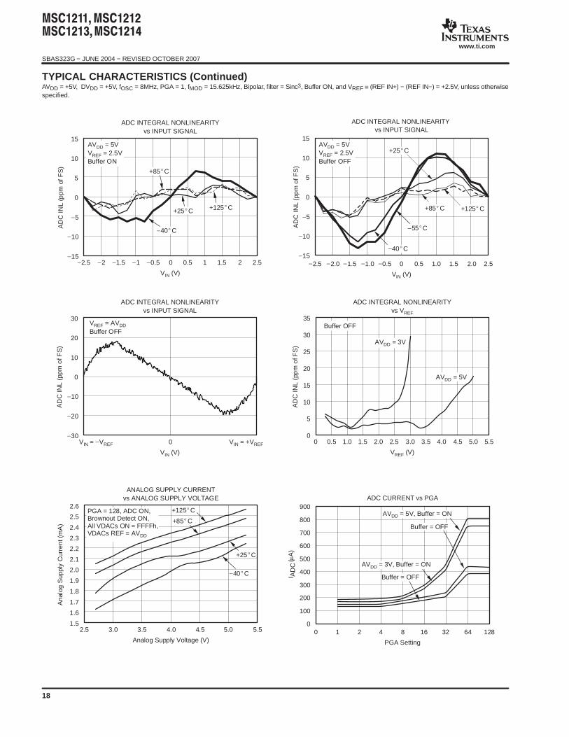
TYPICAL CHARACTERISTICS (Continued)AVDD = +5V, DVDD = +5V, fOSC = 8MHz, PGA = 1, fMOD = 15.625kHz, Bipolar, filter = Sinc3, Buffer ON, and VREF ≡ (REF IN+) − (REF IN−) = +2.5V, unless otherwisespecified.
15
10
5
0
−5
−10
−15
ADC INTEGRAL NONLINEARITYvs INPUT SIGNAL
VIN (V)
−2.5 −2 −1 −0.5−1.5 0 0.5 1 1.5 2 2.5
AD
CIN
L(p
pmof
FS
)
−40C
+25C +125C
+85C
AVDD = 5VVREF = 2.5VBuffer ON
15
10
5
0
−5
−10
−15
ADC INTEGRAL NONLINEARITYvs INPUT SIGNAL
VIN (V)
−2.5 −1.0 −0.5 1.00.5 2.0 2.5−1.5−2.0 0 1.5
AD
CIN
L(p
pm
ofF
S)
AVDD = 5VVREF = 2.5VBuffer OFF
+125C+85C
+25C
−55C
−40C
30
20
10
0
−10
−20
−30
ADC INTEGRAL NONLINEARITYvs INPUT SIGNAL
VIN (V)
VIN = −VREF 0 VIN = +VREF
VREF = AVDDBuffer OFF
AD
CIN
L(p
pmo
fFS
)
35
30
25
20
15
10
5
0
ADC INTEGRAL NONLINEARITYvs VREF
VREF (V)
0 0.5 1.0 1.5 2.0 2.5 3.0 3.5 4.0 4.5 5.0 5.5
AD
CIN
L(p
pm
ofF
S)
Buffer OFF
AVDD = 3V
AVDD = 5V
2.6
2.5
2.4
2.3
2.2
2.1
2.0
1.9
1.8
1.7
1.6
1.5
ANALOG SUPPLY CURRENTvs ANALOG SUPPLY VOLTAGE
Analog Supply Voltage (V)
2.5 3.0 3.5 4.0 4.5 5.0 5.5
Ana
log
Sup
ply
Cur
ren
t(m
A)
PGA = 128, ADC ON,Brownout Detect ON,All VDACs ON = FFFFh,VDACs REF = AVDD
−40C
+25C
+85C
+125C 900
800
700
600
500
400
300
200
100
0
ADC CURRENT vs PGA
PGA Setting
0 1 82 4 3216 12864
AVDD = 5V, Buffer = ON
AVDD = 3V, Buffer = ON
Buffer = OFF
Buffer = OFF
I AD
C (µ
A)
SBAS323G − JUNE 2004 − REVISED OCTOBER 2007
www.ti.com
19
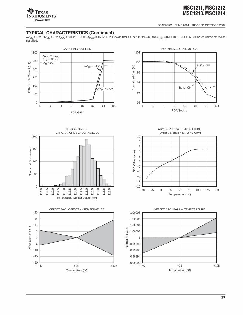
TYPICAL CHARACTERISTICS (Continued)AVDD = +5V, DVDD = +5V, fOSC = 8MHz, PGA = 1, fMOD = 15.625kHz, Bipolar, filter = Sinc3, Buffer ON, and VREF ≡ (REF IN+) − (REF IN−) = +2.5V, unless otherwisespecified.
300
250
200
150
100
50
0
PGA SUPPLY CURRENT
1 42 168 12864
PG
AS
upp
lyC
urre
nt(µ
A)
32
PGA Gain
AVDD = 5.0V
AVDD = 3.0V
AVDD = DVDDfCLK = 8MHzVIN = 0V
NORMALIZED GAIN vs PGA
PGA Setting
Nor
mal
ized
Gai
n(%
)
1 42 168 1286432
101
100
99
98
97
96
Buffer ON
Buffer OFF
200
150
100
50
0
HISTOGRAM OFTEMPERATURE SENSOR VALUES
Temperature Sensor Value (mV)
111
.0
111
.5
112
.0
112
.5
113
.0
113
.5
114
.0
114
.5
115
.0
115
.5
116
.0
116
.5
117
.0
Num
ber
ofO
ccu
rren
ces
10
8
6
4
2
0
−2
−4
−6
−8
−10
ADC OFFSET vs TEMPERATURE(Offset Calibration at +25C Only)
Temperature (C)
−50 0 25 50 75 100 125 150−25
AD
CO
ffset
(ppm
)
20
15
10
5
0
−5
−10
−15
−20
OFFSET DAC: OFFSET vs TEMPERATURE
Offs
et(
ppm
ofF
SR
)
Temperature (C)
−40 +25 +125
OFFSET DAC: GAIN vs TEMPERATURE
Nor
mal
ized
Ga
in
Temperature (C)
−40 +25
1.00008
1.00006
1.00004
1.00002
1
0.99998
0.99996
0.99994
0.99992+125
SBAS323G − JUNE 2004 − REVISED OCTOBER 2007
www.ti.com
20
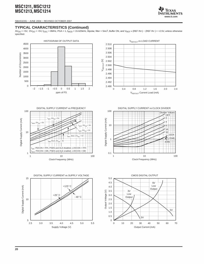
TYPICAL CHARACTERISTICS (Continued)AVDD = +5V, DVDD = +5V, fOSC = 8MHz, PGA = 1, fMOD = 15.625kHz, Bipolar, filter = Sinc3, Buffer ON, and VREF ≡ (REF IN+) − (REF IN−) = +2.5V, unless otherwisespecified.
4500
4000
3500
3000
2500
2000
1500
1000
500
0
HISTOGRAM OF OUTPUT DATA
ppm of FS
−2
Num
ber
ofO
ccur
renc
es
−1.5 −1 −0.5 0 0.5 1 1.5 2
2.510
2.508
2.506
2.504
2.502
2.500
2.498
2.496
2.494
2.492
2.490
VREFOUT vs LOAD CURRENT
VREFOUT Current Load (mA)
0 0.4 0.8 1.2 1.6 2.0 2.4
VR
EF
OU
T(V
)
DIGITAL SUPPLY CURRENT vs FREQUENCY
Clock Frequency (MHz)
Dig
italS
upp
lyC
urr
ent(
mA
)
1 10 100
100
10
1
IMAX, DVDD = 5V
IMAX, DVDD = 3V
IMIN, DVDD = 5V
IMIN, DVDD = 3V
IMIN IDLE, DVDD = 3V
IMAX IDLE, DVDD = 5V
IMIN: PDCON = FFh, PSEN and ALE disabled, LVDCON = FFh
IMAX: PDCON = 00h, PSEN and ALE enabled, LVDCON = 00h
DIGITAL SUPPLY CURRENT vs CLOCK DIVIDER
Clock Frequency (MHz)
Dig
italS
uppl
yC
urre
nt(m
A)
1 10 100
100
10
1
0.1
OFF
4
8
1632
4096
1024
Divider Values
2048
2
DIGITAL SUPPLY CURRENT vs SUPPLY VOLTAGE
Supply Voltage (V)
Dig
italS
uppl
yC
urre
nt(m
A)
2.5 3.0 3.5 4.0 4.5 5.0 5.5
15
10
5
−40C
+125C
+25C
CMOS DIGITAL OUTPUT
Output Current (mA)
Ou
tput
Vol
tage
(V)
0 2010 4030 706050
5.0
4.5
4.0
3.5
3.0
2.5
2.0
1.5
1.0
0.5
0
3VLow
Output
5VLow
Output
5V
3V
SBAS323G − JUNE 2004 − REVISED OCTOBER 2007
www.ti.com
21
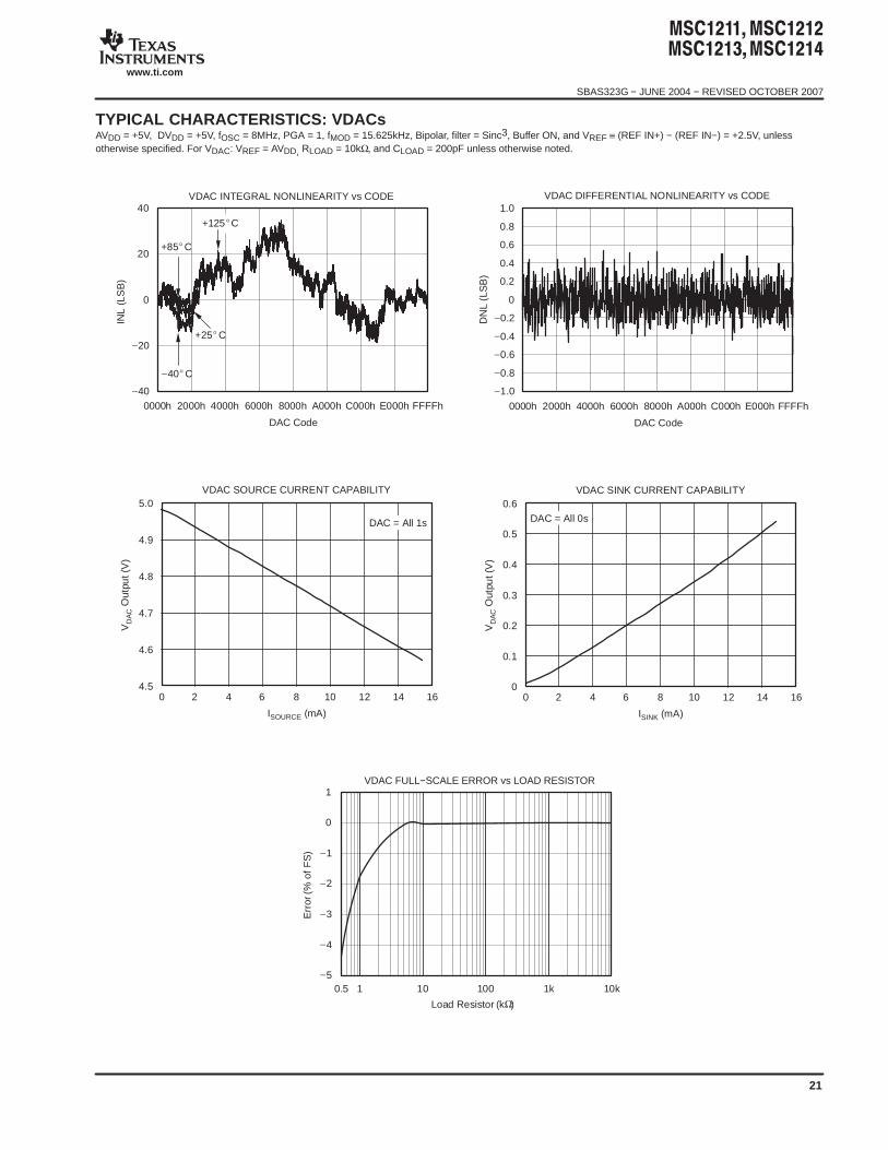
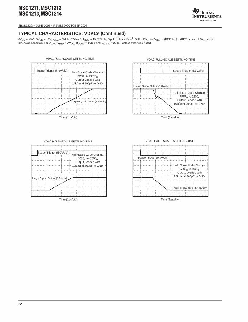
TYPICAL CHARACTERISTICS: VDACsAVDD = +5V, DVDD = +5V, fOSC = 8MHz, PGA = 1, fMOD = 15.625kHz, Bipolar, filter = Sinc3, Buffer ON, and VREF ≡ (REF IN+) − (REF IN−) = +2.5V, unlessotherwise specified. For VDAC: VREF = AVDD, RLOAD = 10kΩ, and CLOAD = 200pF unless otherwise noted.
VDAC INTEGRAL NONLINEARITY vs CODE
0000h
INL
(LS
B)
DAC Code
2000h 4000h 6000h 8000h A000h C000h E000h FFFFh
40
20
0
−20
−40
−40C
+85C
+25C
+125C
VDAC DIFFERENTIAL NONLINEARITY vs CODE
DN
L(L
SB
)
1.0
0.8
0.6
0.4
0.2
0
−0.2
−0.4
−0.6
−0.8
−1.0
0000h
DAC Code
2000h 4000h 6000h 8000h A000h C000h E000h FFFFh
5.0
4.9
4.8
4.7
4.6
4.5
VDAC SOURCE CURRENT CAPABILITY
VD
AC
Out
put(
V)
ISOURCE (mA)
0 4 6 1082 12 14 16
DAC = All 1s
0.6
0.5
0.4
0.3
0.2
0.1
0
VDAC SINK CURRENT CAPABILITYV
DA
CO
utpu
t(V
)
ISINK (mA)
0 4 6 1082 12 14 16
DAC = All 0s
0.5
Err
or(%
ofF
S)
Load Resistor (kΩ)
1 10 100 1k 10k
1
0
−1
−2
−3
−4
−5
VDAC FULL−SCALE ERROR vs LOAD RESISTOR
SBAS323G − JUNE 2004 − REVISED OCTOBER 2007
www.ti.com
22
TYPICAL CHARACTERISTICS: VDACs (Continued)AVDD = +5V, DVDD = +5V, fOSC = 8MHz, PGA = 1, fMOD = 15.625kHz, Bipolar, filter = Sinc3, Buffer ON, and VREF ≡ (REF IN+) − (REF IN−) = +2.5V, unlessotherwise specified. For VDAC: VREF = AVDD, RLOAD = 10kΩ, and CLOAD = 200pF unless otherwise noted.
Scope Trigger (5.0V/div)
Large−Signal Output (1.0V/div)
Full−Scale Code Change0200H to FFFFH
Output Loaded with10kΩand 200pF to GND
Time (1µs/div)
VDAC FULL−SCALE SETTLING TIME
Scope Trigger (5.0V/div)
Large−Signal Output (1.0V/div)
Full−Scale Code ChangeFFFFH to 0200H
Output Loaded with10kΩand 200pF to GND
Time (1µs/div)
VDAC FULL−SCALE SETTLING TIME
Scope Trigger (5.0V/div)
Large−Signal Output (1.0V/div)
Half−Scale Code Change4000H to C000H
Output Loaded with10kΩand 200pF to GND
Time (1µs/div)
VDAC HALF−SCALE SETTLING TIME
Scope Trigger (5.0V/div)
Large−Signal Output (1.0V/div)
Half−Scale Code ChangeC000H to 4000H
Output Loaded with10kΩand 200pF to GND
Time (1µs/div)
VDAC HALF−SCALE SETTLING TIME
SBAS323G − JUNE 2004 − REVISED OCTOBER 2007
www.ti.com
23
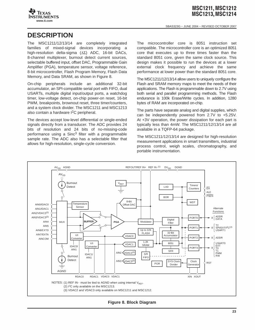
DESCRIPTIONThe MSC1211/12/13/14 are completely integratedfamilies of mixed-signal devices incorporating ahigh-resolution delta-sigma (∆Σ) ADC, 16-bit DACs,8-channel multiplexer, burnout detect current sources,selectable buffered input, offset DAC, Programmable GainAmplifier (PGA), temperature sensor, voltage reference,8-bit microcontroller, Flash Program Memory, Flash DataMemory, and Data SRAM, as shown in Figure 8.
On-chip peripherals include an additional 32-bitaccumulator, an SPI-compatible serial port with FIFO, dualUSARTs, multiple digital input/output ports, a watchdogtimer, low-voltage detect, on-chip power-on reset, 16-bitPWM, breakpoints, brownout reset, three timer/counters,and a system clock divider. The MSC1211 and MSC1213also contain a hardware I2C peripheral.
The devices accept low-level differential or single-endedsignals directly from a transducer. The ADC provides 24bits of resolution and 24 bits of no-missing-codeperformance using a Sinc3 filter with a programmablesample rate. The ADC also has a selectable filter thatallows for high-resolution, single-cycle conversion.
The microcontroller core is 8051 instruction setcompatible. The microcontroller core is an optimized 8051core that executes up to three times faster than thestandard 8051 core, given the same clock source. Thisdesign makes it possible to run the devices at a lowerexternal clock frequency and achieve the sameperformance at lower power than the standard 8051 core.
The MSC1211/12/13/14 allow users to uniquely configure theFlash and SRAM memory maps to meet the needs of theirapplications. The Flash is programmable down to 2.7V usingboth serial and parallel programming methods. The Flashendurance is 100k Erase/Write cycles. In addition, 1280bytes of RAM are incorporated on-chip.
The parts have separate analog and digital supplies, whichcan be independently powered from 2.7V to +5.25V.At +3V operation, the power dissipation for each part istypically less than 4mW. The MSC1211/12/13/14 are allavailable in a TQFP-64 package.
The MSC1211/12/13/14 are designed for high-resolutionmeasurement applications in smart transmitters, industrialprocess control, weigh scales, chromatography, andportable instrumentation.
PGA
32−BitAccumulator
MUX
AVDD
VREF
Modulator
Up to 32KFLASH
1.2KSRAM
SPIFIFO
DigitalFilter
8051
SFR
SYS ClockDivider
LVD
BOR
POR
PORT1
PORT2
WDT
Timers/Counters
ClockGenerator
PORT0
PORT3
8
8
8
EA
8
T2SPI/EXT/I2C(2)
USART1
ADDR
ADDRDATA
AlternateFunctions
USART0EXTT0T1PWMRW
8−BitOffset DACAIN0/IDAC0
AIN1/IDAC1
AIN2/VDAC2(3)
AIN3/VDAC3(3)
AIN4
AIN5
AIN6/EXTD
AIN7/EXTA
AINCOM
AGND REFOUT/REF IN+ REF IN−(1) DVDD DGND
XIN XOUT
VDAC0
VDAC1
VDAC2(3)
VDAC3(3)
AIN2
AIN3
VDAC1VDAC0
ALE
PSEN
V/IConverter
V/IConverter
TemperatureSensor
RST
RDAC1
IDAC1/AIN1
RDAC0
IDAC0/AIN1
BurnoutDetect
BurnoutDetect
AGND
AVDD
(1) REF IN− must be tied to AGND when using internal VREF.(2) I2C only available on the MSC1213.(3) VDAC2 and VDAC3 only available on MSC1211 and MSC1212.
BUFFER
NOTES:
Figure 8. Block Diagram
SBAS323G − JUNE 2004 − REVISED OCTOBER 2007
www.ti.com
24
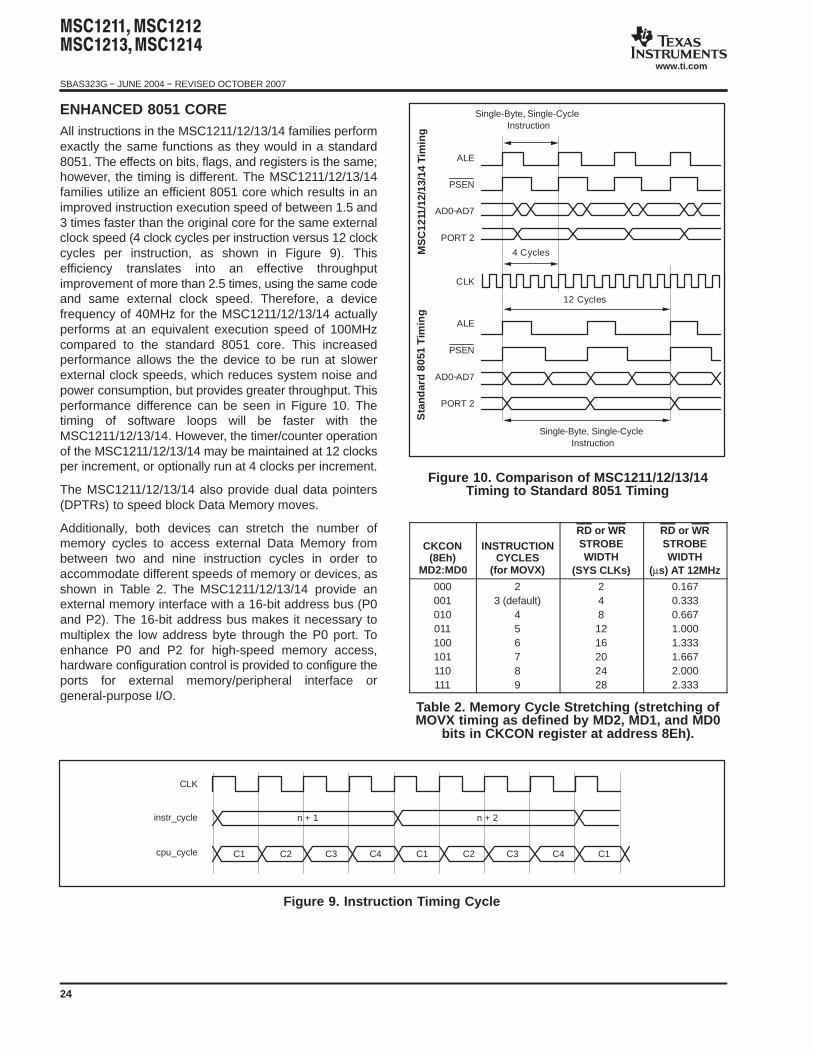
ENHANCED 8051 COREAll instructions in the MSC1211/12/13/14 families performexactly the same functions as they would in a standard8051. The effects on bits, flags, and registers is the same;however, the timing is different. The MSC1211/12/13/14families utilize an efficient 8051 core which results in animproved instruction execution speed of between 1.5 and3 times faster than the original core for the same externalclock speed (4 clock cycles per instruction versus 12 clockcycles per instruction, as shown in Figure 9). Thisefficiency translates into an effective throughputimprovement of more than 2.5 times, using the same codeand same external clock speed. Therefore, a devicefrequency of 40MHz for the MSC1211/12/13/14 actuallyperforms at an equivalent execution speed of 100MHzcompared to the standard 8051 core. This increasedperformance allows the the device to be run at slowerexternal clock speeds, which reduces system noise andpower consumption, but provides greater throughput. Thisperformance difference can be seen in Figure 10. Thetiming of software loops will be faster with theMSC1211/12/13/14. However, the timer/counter operationof the MSC1211/12/13/14 may be maintained at 12 clocksper increment, or optionally run at 4 clocks per increment.
The MSC1211/12/13/14 also provide dual data pointers(DPTRs) to speed block Data Memory moves.
Additionally, both devices can stretch the number ofmemory cycles to access external Data Memory frombetween two and nine instruction cycles in order toaccommodate different speeds of memory or devices, asshown in Table 2. The MSC1211/12/13/14 provide anexternal memory interface with a 16-bit address bus (P0and P2). The 16-bit address bus makes it necessary tomultiplex the low address byte through the P0 port. Toenhance P0 and P2 for high-speed memory access,hardware configuration control is provided to configure theports for external memory/peripheral interface orgeneral-purpose I/O.
ALE
PSEN
AD0−AD7
PORT 2
ALE
PSEN
AD0−AD7
PORT 2
CLK
Sta
ndar
d80
51T
imin
g
12 Cycles
4 Cycles
Single-Byte, Single-Cycle Instruction
Single-Byte, Single-Cycle Instruction
MS
C12
11/1
2/13
/14
Tim
ing
Figure 10. Comparison of MSC1211/12/13/14Timing to Standard 8051 Timing
CKCON(8Eh)
MD2:MD0
INSTRUCTIONCYCLES
(for MOVX)
RD or WRSTROBEWIDTH
(SYS CLKs)
RD or WRSTROBEWIDTH
(µs) AT 12MHz
000 2 2 0.167001 3 (default) 4 0.333010 4 8 0.667011 5 12 1.000100 6 16 1.333101 7 20 1.667110 8 24 2.000111 9 28 2.333
Table 2. Memory Cycle Stretching (stretching ofMOVX timing as defined by MD2, MD1, and MD0
bits in CKCON register at address 8Eh).
CLK
instr_cycle
cpu_cycle C1 C2 C3 C4 C1 C2 C3 C4 C1
n + 1 n + 2
Figure 9. Instruction Timing Cycle
SBAS323G − JUNE 2004 − REVISED OCTOBER 2007
www.ti.com
25
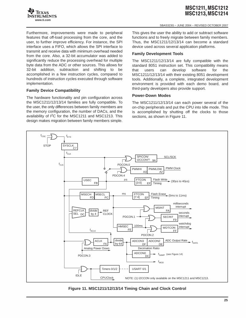
Furthermore, improvements were made to peripheralfeatures that off-load processing from the core, and theuser, to further improve efficiency. For instance, the SPIinterface uses a FIFO, which allows the SPI interface totransmit and receive data with minimum overhead neededfrom the core. Also, a 32-bit accumulator was added tosignificantly reduce the processing overhead for multiplebyte data from the ADC or other sources. This allows for32-bit addition, subtraction and shifting to beaccomplished in a few instruction cycles, compared tohundreds of instruction cycles executed through softwareimplementation.
Family Device Compatibility
The hardware functionality and pin configuration acrossthe MSC1211/12/13/14 families are fully compatible. Tothe user, the only differences between family members arethe memory configuration, the number of DACs, and theavailability of I2C for the MSC1211 and MSC1213. Thisdesign makes migration between family members simple.
This gives the user the ability to add or subtract softwarefunctions and to freely migrate between family members.Thus, the MSC1211/12/13/14 can become a standarddevice used across several application platforms.
Family Development Tools
The MSC1211/12/13/14 are fully compatible with thestandard 8051 instruction set. This compatibility meansthat users can develop software for theMSC1211/12/13/14 with their existing 8051 developmenttools. Additionally, a complete, integrated developmentenvironment is provided with each demo board, andthird-party developers also provide support.
Power-Down Modes
The MSC1211/12/13/14 can each power several of theon-chip peripherals and put the CPU into Idle mode. Thisis accomplished by shutting off the clocks to thosesections, as shown in Figure 11.
(see Figure 14)
USECFB
MSECH
HMSECFE
MSINTFA
ACLKF6
divideby 64
divideby 4
MSECLFD FC
ms
µs
100ms
Flash WriteTiming
Flash EraseTiming
WDTCON
SECINTF9
FF
FTCON[3:0]
FTCON[7:4]
EF
EF
secondsinterrupt
watchdoginterrupt
millisecondsinterrupt
ADC Output RateADCON3 ADCON2DF DE
Decimation Ratio
SPICON/I2CCON(1) 9A
SCL/SCKfCLK
fSYS
(30µs to 40µs)
(5ms to 11ms)
PDCON.0
PDCON.1
PDCON.2
PDCON.3
IDLECPUClock
Timers 0/1/2
SYSCLK
Analog Power Down
USART 0/1
REFCLOCK
REFCLKSEL
fACLK
fDATA
fSAMP
fMOD
fCLK
STOP
fOSC
C7
PDCON.4
PWMHI PWMLOWA3 A2
PWM Clock
ADCON0DC
DC
NOTE: (1) I2CCON only available on the MSC1211 and MSC1213.
Figure 11. MSC1211/12/13/14 Timing Chain and Clock Control
SBAS323G − JUNE 2004 − REVISED OCTOBER 2007
www.ti.com
26
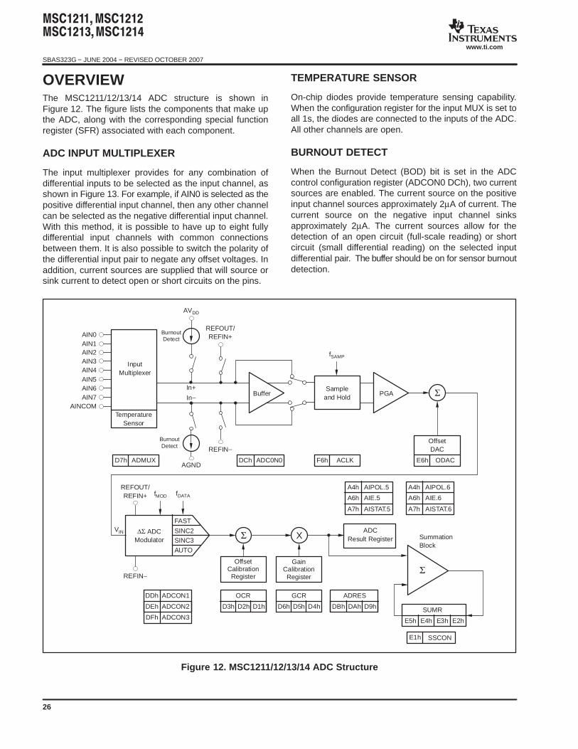
OVERVIEWThe MSC1211/12/13/14 ADC structure is shown inFigure 12. The figure lists the components that make upthe ADC, along with the corresponding special functionregister (SFR) associated with each component.
ADC INPUT MULTIPLEXER
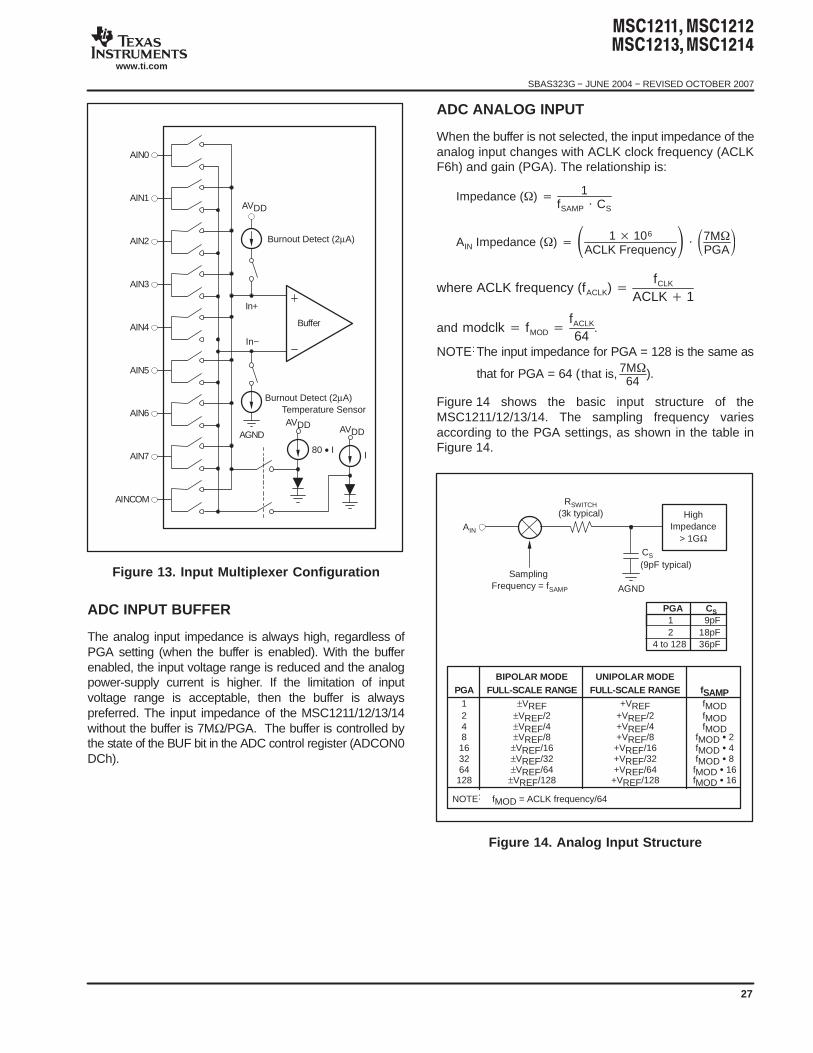
The input multiplexer provides for any combination ofdifferential inputs to be selected as the input channel, asshown in Figure 13. For example, if AIN0 is selected as thepositive differential input channel, then any other channelcan be selected as the negative differential input channel.With this method, it is possible to have up to eight fullydifferential input channels with common connectionsbetween them. It is also possible to switch the polarity ofthe differential input pair to negate any offset voltages. Inaddition, current sources are supplied that will source orsink current to detect open or short circuits on the pins.
TEMPERATURE SENSOR
On-chip diodes provide temperature sensing capability.When the configuration register for the input MUX is set toall 1s, the diodes are connected to the inputs of the ADC.All other channels are open.
BURNOUT DETECT
When the Burnout Detect (BOD) bit is set in the ADCcontrol configuration register (ADCON0 DCh), two currentsources are enabled. The current source on the positiveinput channel sources approximately 2µA of current. Thecurrent source on the negative input channel sinksapproximately 2µA. The current sources allow for thedetection of an open circuit (full-scale reading) or shortcircuit (small differential reading) on the selected inputdifferential pair. The buffer should be on for sensor burnoutdetection.
Σ
Σ X
InputMultiplexer
TemperatureSensor
Buffer PGASample
and Hold
ADMUXD7h
REFOUT/REFIN+
REFIN−
REFOUT/REFIN+ fMOD
REFIN−
AIN5AIN6AIN7
AINCOM
ADCON1DDh
ADCON2DEh
ADCON3DFh
OCR GCR ADRES
SUMRD3h D2h D1h D6h D5h D4h DBh DAh D9h
E5h E4h E3h E2h
OffsetCalibrationRegister
ADC0N0DCh ACLKF6h
SSCONE1h
ODACE6h
OffsetDAC
∆Σ ADCModulator
FAST
SINC2SINC3
AUTO
ADCResult Register
Σ
SummationBlock
VIN
AIN2AIN3AIN4
AIN0AIN1
fSAMP
fDATA
GainCalibrationRegister
BurnoutDetect
AVDD
In+
AGND
In−
BurnoutDetect
AIPOL.5A4h
AISTAT.5A7h
AIE.5A6h
AIPOL.6A4h
AISTAT.6A7h
AIE.6A6h
Figure 12. MSC1211/12/13/14 ADC Structure
SBAS323G − JUNE 2004 − REVISED OCTOBER 2007
www.ti.com
27
AIN3
AIN4
AIN5
AIN6
AIN0
AIN1
AIN2
AIN7
AINCOM
AGND
Buffer
I
In+
Burnout Detect (2µA)
Burnout Detect (2µA)Temperature Sensor
80 • I
AVDD
AVDD AVDD
In−
Figure 13. Input Multiplexer Configuration
ADC INPUT BUFFER
The analog input impedance is always high, regardless ofPGA setting (when the buffer is enabled). With the bufferenabled, the input voltage range is reduced and the analogpower-supply current is higher. If the limitation of inputvoltage range is acceptable, then the buffer is alwayspreferred. The input impedance of the MSC1211/12/13/14without the buffer is 7MΩ/PGA. The buffer is controlled bythe state of the BUF bit in the ADC control register (ADCON0DCh).
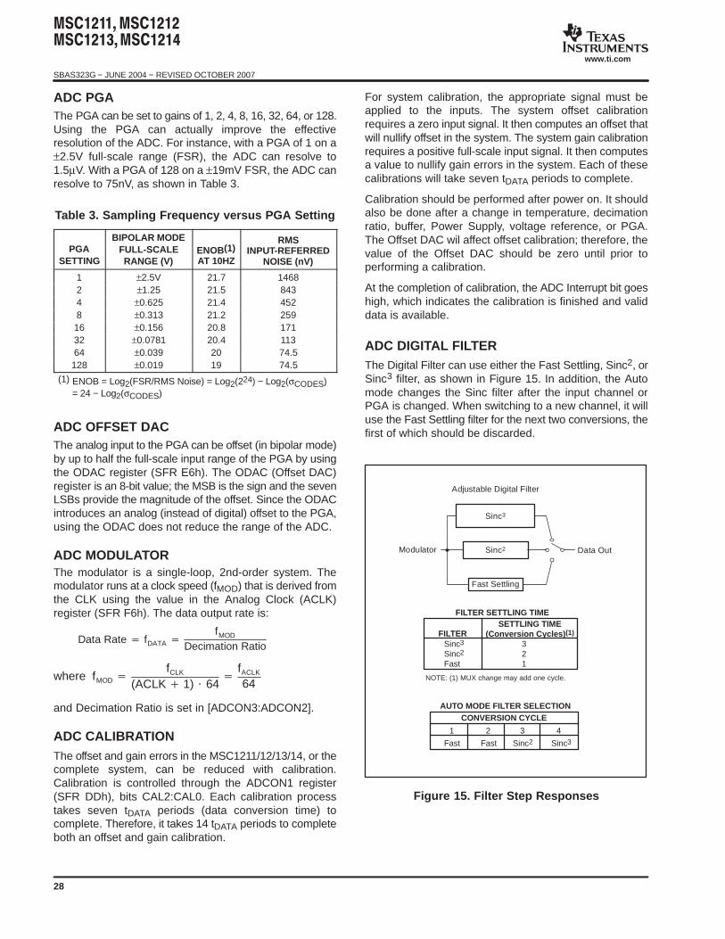
ADC ANALOG INPUT
When the buffer is not selected, the input impedance of theanalog input changes with ACLK clock frequency (ACLKF6h) and gain (PGA). The relationship is:
Impedance () 1fSAMP CS
AIN Impedance () 1 106
ACLK Frequency 7M
PGA
where ACLK frequency (fACLK) fCLK
ACLK 1
and modclk fMOD fACLK
64.
NOTE: The input impedance for PGA = 128 is the same as
that for PGA = 64 ( that is, 7M
64).
Figure 14 shows the basic input structure of theMSC1211/12/13/14. The sampling frequency variesaccording to the PGA settings, as shown in the table inFigure 14.
BIPOLAR MODE UNIPOLAR MODEPGA FULL-SCALE RANGE FULL-SCALE RANGE f SAMP
1 ±VREF +VREF fMOD2 ±VREF/2 +VREF/2 fMOD4 ±VREF/4 +VREF/4 fMOD8 ±VREF/8 +VREF/8 fMOD 216 ±VREF/16 +VREF/16 fMOD 432 ±VREF/32 +VREF/32 fMOD 864 ±VREF/64 +VREF/64 fMOD 16128 ±VREF/128 +VREF/128 fMOD 16
NOTE: fMOD = ACLK frequency/64
RSWITCH(3k typical)
SamplingFrequency = fSAMP
HighImpedance
> 1GΩCS
AGND
AIN
(9pF typical)
PGA CS1 9pF2 18pF
4 to 128 36pF
Figure 14. Analog Input Structure
SBAS323G − JUNE 2004 − REVISED OCTOBER 2007
www.ti.com
28
ADC PGAThe PGA can be set to gains of 1, 2, 4, 8, 16, 32, 64, or 128.Using the PGA can actually improve the effectiveresolution of the ADC. For instance, with a PGA of 1 on a±2.5V full-scale range (FSR), the ADC can resolve to1.5µV. With a PGA of 128 on a ±19mV FSR, the ADC canresolve to 75nV, as shown in Table 3.
Table 3. Sampling Frequency versus PGA Setting
PGASETTING
BIPOLAR MODEFULL-SCALERANGE (V)
ENOB(1)AT 10HZ
RMSINPUT-REFERRED
NOISE (nV)
1 ±2.5V 21.7 14682 ±1.25 21.5 8434 ±0.625 21.4 4528 ±0.313 21.2 25916 ±0.156 20.8 17132 ±0.0781 20.4 11364 ±0.039 20 74.5128 ±0.019 19 74.5
(1) ENOB = Log2(FSR/RMS Noise) = Log2(224) − Log2(σCODES)= 24 − Log2(σCODES)
ADC OFFSET DACThe analog input to the PGA can be offset (in bipolar mode)by up to half the full-scale input range of the PGA by usingthe ODAC register (SFR E6h). The ODAC (Offset DAC)register is an 8-bit value; the MSB is the sign and the sevenLSBs provide the magnitude of the offset. Since the ODACintroduces an analog (instead of digital) offset to the PGA,using the ODAC does not reduce the range of the ADC.
ADC MODULATORThe modulator is a single-loop, 2nd-order system. Themodulator runs at a clock speed (fMOD) that is derived fromthe CLK using the value in the Analog Clock (ACLK)register (SFR F6h). The data output rate is:
Data Rate fDATA fMOD
Decimation Ratio
where fMOD fCLK
(ACLK 1) 64
fACLK
64
and Decimation Ratio is set in [ADCON3:ADCON2].
ADC CALIBRATIONThe offset and gain errors in the MSC1211/12/13/14, or thecomplete system, can be reduced with calibration.Calibration is controlled through the ADCON1 register(SFR DDh), bits CAL2:CAL0. Each calibration processtakes seven tDATA periods (data conversion time) tocomplete. Therefore, it takes 14 tDATA periods to completeboth an offset and gain calibration.
For system calibration, the appropriate signal must beapplied to the inputs. The system offset calibrationrequires a zero input signal. It then computes an offset thatwill nullify offset in the system. The system gain calibrationrequires a positive full-scale input signal. It then computesa value to nullify gain errors in the system. Each of thesecalibrations will take seven tDATA periods to complete.
Calibration should be performed after power on. It shouldalso be done after a change in temperature, decimationratio, buffer, Power Supply, voltage reference, or PGA.The Offset DAC wil affect offset calibration; therefore, thevalue of the Offset DAC should be zero until prior toperforming a calibration.
At the completion of calibration, the ADC Interrupt bit goeshigh, which indicates the calibration is finished and validdata is available.
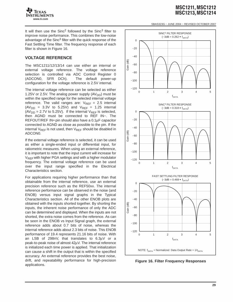
ADC DIGITAL FILTERThe Digital Filter can use either the Fast Settling, Sinc2, orSinc3 filter, as shown in Figure 15. In addition, the Automode changes the Sinc filter after the input channel orPGA is changed. When switching to a new channel, it willuse the Fast Settling filter for the next two conversions, thefirst of which should be discarded.
Adjustable Digital Filter
Data OutModulator
Fast Settling
Sinc2
Sinc3
Fast Fast Sinc2 Sinc3
1 2 3 4
FILTERSETTLING TIME
(Conversion Cycles) (1)
Sinc3 Sinc2 Fast
321
NOTE: (1) MUX change may add one cycle.
CONVERSION CYCLEAUTO MODE FILTER SELECTION
FILTER SETTLING TIME
Figure 15. Filter Step Responses
SBAS323G − JUNE 2004 − REVISED OCTOBER 2007
www.ti.com
29
It will then use the Sinc2 followed by the Sinc3 filter toimprove noise performance. This combines the low-noiseadvantage of the Sinc3 filter with the quick response of theFast Settling Time filter. The frequency response of eachfilter is shown in Figure 16.
VOLTAGE REFERENCE
The MSC1211/12/13/14 can use either an internal orexternal voltage reference. The voltage referenceselection is controlled via ADC Control Register 0(ADCON0, SFR DCh). The default power-upconfiguration for the voltage reference is 2.5V internal.
The internal voltage reference can be selected as either1.25V or 2.5V. The analog power supply (AVDD) must bewithin the specified range for the selected internal voltagereference. The valid ranges are: VREF = 2.5 internal(AVDD = 3.3V to 5.25V) and VREF = 1.25 internal(AVDD = 2.7V to 5.25V). If the internal VREF is selected,then AGND must be connected to REF IN−. TheREFOUT/REF IN+ pin should also have a 0.1µF capacitorconnected to AGND as close as possible to the pin. If theinternal VREF is not used, then VREF should be disabled inADCON0.
If the external voltage reference is selected, it can be usedas either a single-ended input or differential input, forratiometric measures. When using an external reference,it is important to note that the input current will increase forVREF with higher PGA settings and with a higher modulatorfrequency. The external voltage reference can be usedover the input range specified in the ElectricalCharacteristics section.
For applications requiring higher performance than thatobtainable from the internal reference, use an externalprecision reference such as the REF50xx. The internalreference performance can be observed in the noise (andENOB) versus input signal graphs in the TypicalCharacteristics section. All of the other ENOB plots areobtained with the inputs shorted together. By shorting theinputs, the inherent noise performance of only the ADCcan be determined and displayed. When the inputs are notshorted, the extra noise comes from the reference. As canbe seen in the ENOB vs Input Signal graph, the externalreference adds about 0.7 bits of noise, whereas theinternal reference adds about 2.3 bits of noise. This ENOBperformance of 19.4 represents 21.16 bits of noise. Withan LSB of 298nV, that translates to 6.3µV or apeak-to-peak noise of almost 42µV. The internal referenceis initialized each time power is applied. That initializationcan cause a shift in the output that is within the specifiedaccuracy. An external reference provides the best noise,drift, and repeatability performance for high-precisionapplications.
SINC3 FILTER RESPONSE(−3dB = 0.262 • fDATA)
fDATA
0
−20
−40
−60
−80
−100
−1200 1 2 3 4 5
0 1 2 3 4 5
0 1 2 3 4 5
Gai
n(d
B)
SINC2 FILTER RESPONSE(−3dB = 0.318 • fDATA)
fDATA
0
−20
−40
−60
−80
−100
−120
Gai
n(d
B)
FAST SETTLING FILTER RESPONSE(−3dB = 0.469 • fDATA)
fDATA
0
−20
−40
−60
−80
−100
−120
NOTE: fDATA = Normalized Data Output Rate = 1/tDATA
Gai
n(d
B)
Figure 16. Filter Frequency Responses
SBAS323G − JUNE 2004 − REVISED OCTOBER 2007
www.ti.com
30
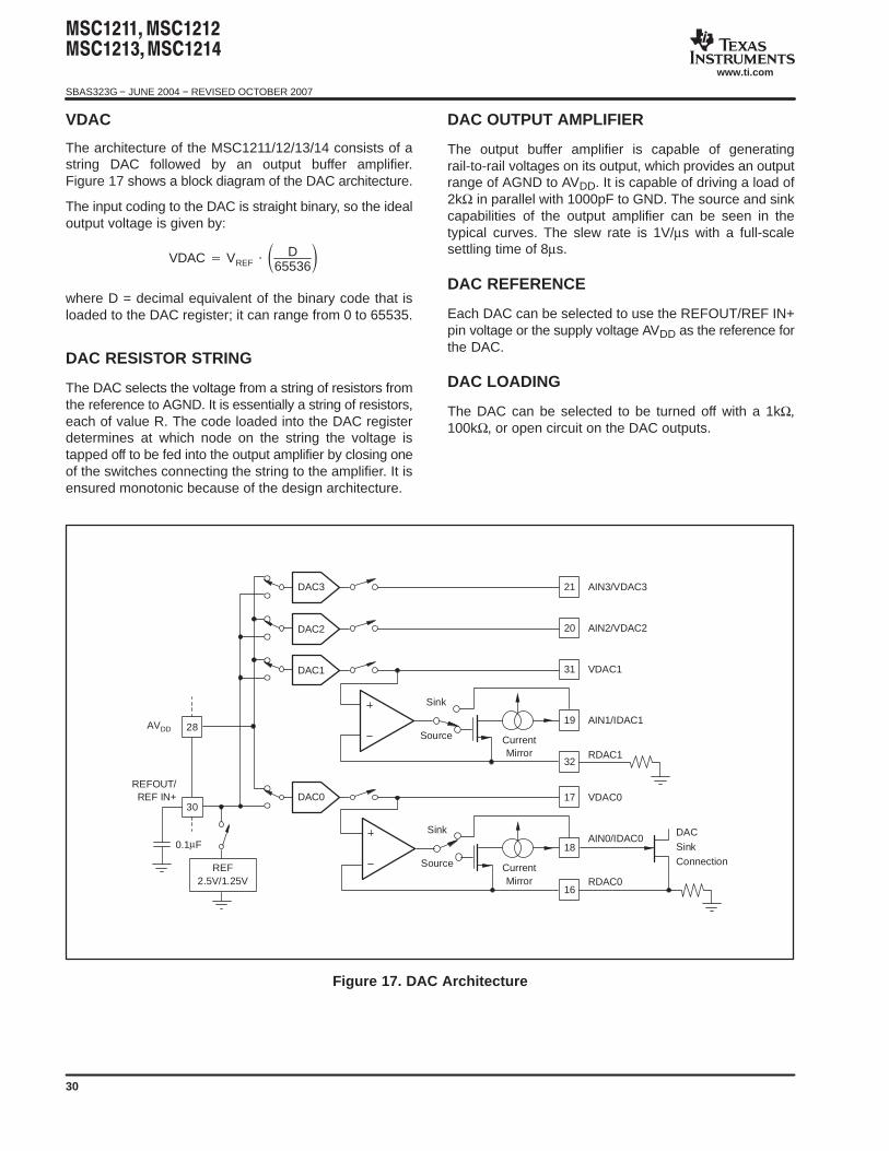
VDAC
The architecture of the MSC1211/12/13/14 consists of astring DAC followed by an output buffer amplifier.Figure 17 shows a block diagram of the DAC architecture.
The input coding to the DAC is straight binary, so the idealoutput voltage is given by:
VDAC VREF D65536
where D = decimal equivalent of the binary code that isloaded to the DAC register; it can range from 0 to 65535.
DAC RESISTOR STRING
The DAC selects the voltage from a string of resistors fromthe reference to AGND. It is essentially a string of resistors,each of value R. The code loaded into the DAC registerdetermines at which node on the string the voltage istapped off to be fed into the output amplifier by closing oneof the switches connecting the string to the amplifier. It isensured monotonic because of the design architecture.
DAC OUTPUT AMPLIFIER
The output buffer amplifier is capable of generatingrail-to-rail voltages on its output, which provides an outputrange of AGND to AVDD. It is capable of driving a load of2kΩ in parallel with 1000pF to GND. The source and sinkcapabilities of the output amplifier can be seen in thetypical curves. The slew rate is 1V/µs with a full-scalesettling time of 8µs.
DAC REFERENCE
Each DAC can be selected to use the REFOUT/REF IN+pin voltage or the supply voltage AVDD as the reference forthe DAC.
DAC LOADING
The DAC can be selected to be turned off with a 1kΩ,100kΩ, or open circuit on the DAC outputs.
DAC3
DAC2
DAC1
DAC0
21 AIN3/VDAC3
AIN2/VDAC2
VDAC1
VDAC0
DACSinkConnection
AIN0/IDAC0
RDAC0
AIN1/IDAC1
RDAC1
20
31
19
32
17
CurrentMirror
CurrentMirror
18
16
Sink
Source
Sink
Source
REFOUT/REF IN+
AVDD
30
REF2.5V/1.25V
28
0.1µF
Figure 17. DAC Architecture
SBAS323G − JUNE 2004 − REVISED OCTOBER 2007
www.ti.com
31
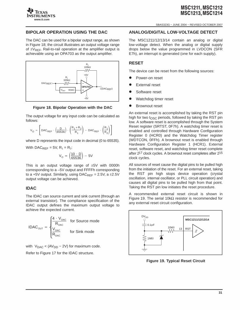
BIPOLAR OPERATION USING THE DAC
The DAC can be used for a bipolar output range, as shownin Figure 18; the circuit illustrates an output voltage rangeof ±VREF. Rail-to-rail operation at the amplifier output isachievable using an OPA703 as the output amplifier.
VREF VDAC
R1100kΩ
R2100kΩ
OPA703
DACREF
±(DACREF)
+6V
−6V
Figure 18. Bipolar Operation with the DAC
The output voltage for any input code can be calculated asfollows:
VO DACREF D65536
R1R2
R1 DACREF R1
R2
where D represents the input code in decimal (0 to 65535).
With DACREF = 5V, R1 = R2:
VO 10 D65536
5V
This is an output voltage range of ±5V with 0000hcorresponding to a –5V output and FFFFh correspondingto a +5V output. Similarly, using DACREF = 2.5V, a ±2.5Voutput voltage can be achieved.
IDAC
The IDAC can source current and sink current (through anexternal transistor). The compliance specification of theIDAC output defines the maximum output voltage toachieve the expected current.
IDACOUT
4 VDAC
RDAC
for Source mode
VDAC
RDAC
for Sink mode
with VDAC < (AVDD − 2V) for maximum code.
Refer to Figure 17 for the IDAC structure.
ANALOG/DIGITAL LOW-VOLTAGE DETECT
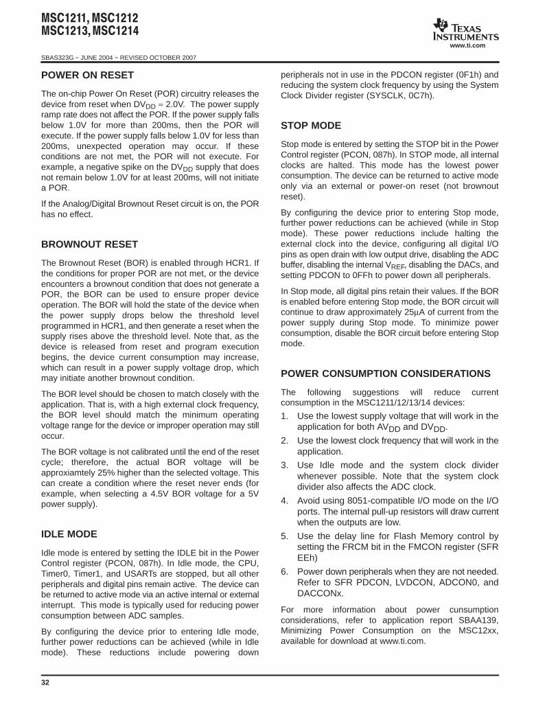
The MSC1211/12/13/14 contain an analog or digitallow-voltage detect. When the analog or digital supplydrops below the value programmed in LVDCON (SFRE7h), an interrupt is generated (one for each supply).
RESET
The device can be reset from the following sources:
Power-on reset
External reset
Software reset
Watchdog timer reset
Brownout reset
An external reset is accomplished by taking the RST pinhigh for two tOSC periods, followed by taking the RST pinlow. A software reset is accomplished through the SystemReset register (SRTST, 0F7h). A watchdog timer reset isenabled and controlled through Hardware ConfigurationRegister 0 (HCR0) and the Watchdog Timer register(WDTCON, 0FFh). A brownout reset is enabled throughHardware Configuration Register 1 (HCR1). Externalreset, software reset, and watchdog timer reset completeafter 217 clock cycles. A brownout reset completes after 215
clock cycles.
All sources of reset cause the digital pins to be pulled highfrom the initiation of the reset. For an external reset, takingthe RST pin high stops device operation (crystaloscillation, internal oscillator, or PLL circuit operation) andcauses all digital pins to be pulled high from that point.Taking the RST pin low initiates the reset procedure.
A recommended external reset circuit is shown inFigure 19. The serial 10kΩ resistor is recommended forany external reset circuit configuration.
10kΩ13 RST
MSC1211/12/13/14
0.1µF
1MΩ
DVDD
Figure 19. Typical Reset Circuit
SBAS323G − JUNE 2004 − REVISED OCTOBER 2007
www.ti.com
32
POWER ON RESET
The on-chip Power On Reset (POR) circuitry releases thedevice from reset when DVDD ≈ 2.0V. The power supplyramp rate does not affect the POR. If the power supply fallsbelow 1.0V for more than 200ms, then the POR willexecute. If the power supply falls below 1.0V for less than200ms, unexpected operation may occur. If theseconditions are not met, the POR will not execute. Forexample, a negative spike on the DVDD supply that doesnot remain below 1.0V for at least 200ms, will not initiatea POR.
If the Analog/Digital Brownout Reset circuit is on, the PORhas no effect.
BROWNOUT RESET
The Brownout Reset (BOR) is enabled through HCR1. Ifthe conditions for proper POR are not met, or the deviceencounters a brownout condition that does not generate aPOR, the BOR can be used to ensure proper deviceoperation. The BOR will hold the state of the device whenthe power supply drops below the threshold levelprogrammed in HCR1, and then generate a reset when thesupply rises above the threshold level. Note that, as thedevice is released from reset and program executionbegins, the device current consumption may increase,which can result in a power supply voltage drop, whichmay initiate another brownout condition.
The BOR level should be chosen to match closely with theapplication. That is, with a high external clock frequency,the BOR level should match the minimum operatingvoltage range for the device or improper operation may stilloccur.
The BOR voltage is not calibrated until the end of the resetcycle; therefore, the actual BOR voltage will beapproxiamtely 25% higher than the selected voltage. Thiscan create a condition where the reset never ends (forexample, when selecting a 4.5V BOR voltage for a 5Vpower supply).
IDLE MODE
Idle mode is entered by setting the IDLE bit in the PowerControl register (PCON, 087h). In Idle mode, the CPU,Timer0, Timer1, and USARTs are stopped, but all otherperipherals and digital pins remain active. The device canbe returned to active mode via an active internal or externalinterrupt. This mode is typically used for reducing powerconsumption between ADC samples.
By configuring the device prior to entering Idle mode,further power reductions can be achieved (while in Idlemode). These reductions include powering down
peripherals not in use in the PDCON register (0F1h) andreducing the system clock frequency by using the SystemClock Divider register (SYSCLK, 0C7h).
STOP MODE
Stop mode is entered by setting the STOP bit in the PowerControl register (PCON, 087h). In STOP mode, all internalclocks are halted. This mode has the lowest powerconsumption. The device can be returned to active modeonly via an external or power-on reset (not brownoutreset).
By configuring the device prior to entering Stop mode,further power reductions can be achieved (while in Stopmode). These power reductions include halting theexternal clock into the device, configuring all digital I/Opins as open drain with low output drive, disabling the ADCbuffer, disabling the internal VREF, disabling the DACs, andsetting PDCON to 0FFh to power down all peripherals.
In Stop mode, all digital pins retain their values. If the BORis enabled before entering Stop mode, the BOR circuit willcontinue to draw approximately 25µA of current from thepower supply during Stop mode. To minimize powerconsumption, disable the BOR circuit before entering Stopmode.
POWER CONSUMPTION CONSIDERATIONS
The following suggestions will reduce currentconsumption in the MSC1211/12/13/14 devices:
1. Use the lowest supply voltage that will work in theapplication for both AVDD and DVDD.
2. Use the lowest clock frequency that will work in theapplication.
3. Use Idle mode and the system clock dividerwhenever possible. Note that the system clockdivider also affects the ADC clock.
4. Avoid using 8051-compatible I/O mode on the I/Oports. The internal pull-up resistors will draw currentwhen the outputs are low.
5. Use the delay line for Flash Memory control bysetting the FRCM bit in the FMCON register (SFREEh)
6. Power down peripherals when they are not needed.Refer to SFR PDCON, LVDCON, ADCON0, andDACCONx.
For more information about power cunsumptionconsiderations, refer to application report SBAA139,Minimizing Power Consumption on the MSC12xx,available for download at www.ti.com.
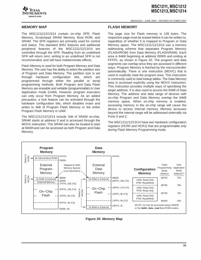
SBAS323G − JUNE 2004 − REVISED OCTOBER 2007
www.ti.com
33
MEMORY MAP
The MSC1211/12/13/14 contain on-chip SFR, FlashMemory, Scratchpad SRAM Memory, Boot ROM, andSRAM. The SFR registers are primarily used for controland status. The standard 8051 features and additionalperipheral features of the MSC1211/12/13/14 arecontrolled through the SFR. Reading from an undefinedSFR will return zero; writing to an undefined SFR is notrecommended, and will have indeterminate effects.
Flash Memory is used for both Program Memory and DataMemory. The user has the ability to select the partition sizeof Program and Data Memory. The partition size is setthrough hardware configuration bits, which areprogrammed through either the parallel or serialprogramming methods. Both Program and Data FlashMemory are erasable and writable (programmable) in UserApplication mode (UAM). However, program executioncan only occur from Program Memory. As an addedprecaution, a lock feature can be activated through thehardware configuration bits, which disables erase andwrites to 4kB of Program Flash Memory or the entireProgram Flash Memory in UAM.
The MSC1211/12/13/14 include 1kB of SRAM on-chip.SRAM starts at address 0 and is accessed through theMOVX instruction. This SRAM can also be located to startat 8400h and can be accessed as both Program and DataMemory.
FLASH MEMORY
The page size for Flash memory is 128 bytes. Therespective page must be erased before it can be written to,regardless of whether it is mapped to Program or DataMemory space. The MSC1211/12/13/14 use a memoryaddressing scheme that separates Program Memory(FLASH/ROM) from Data Memory (FLASH/RAM). Eacharea is 64kB beginning at address 0000h and ending atFFFFh, as shown in Figure 20. The program and datasegments can overlap since they are accessed in differentways. Program Memory is fetched by the microcontrollerautomatically. There is one instruction (MOVC) that isused to explicitly read the program area. This instructionis commonly used to read lookup tables. The Data Memoryarea is accessed explicitly using the MOVX instruction.This instruction provides multiple ways of specifying thetarget address. It is also used to access the 64kB of DataMemory. The address and data range of devices withon-chip Program and Data Memory overlap the 64kBmemory space. When on-chip memory is enabled,accessing memory in the on-chip range will cause thedevice to access internal memory. Memory accessesbeyond the internal range will be addressed externally viaPorts 0 and 2.
The MSC1211/12/13/14 have two hardware configurationregisters (HCR0 and HCR1) that are programmable onlyduring Flash Memory Programming mode.
1k RAM or External1k RAM or External
1k RAM or External
External MemorySel
ect
inM
CO
NS
elec
tin
HC
R0
0000h, 0k
1FFFh, 8k (Y3)
0FFFh, 4k (Y2)
3FFFh, 16k (Y4)
8400h7FFFh, 32k (Y5)
2k Internal Boot ROMF800h
FFFFh
ExternalProgramMemory
Mapped to BothMemory Spaces(von Neumann)
8800h
Se
lect
inM
CO
N
03FFh, 1k
13FFh, 5k (Y2)
23FFh, 9k (Y3)
43FFh, 17k (Y4)
83FFh, 33k (Y5)
FFFFh
ExternalData
Memory
ProgramMemory
DataMemory
8800h
On−ChipFlash
On−ChipFlash
FlashProgramming
ModeAddress
UserApplication
ModeAddress(1)
NOTE: (1) Can be accessed using CADDRor the faddr_data_read Boot ROM routine.
UAM: Read OnlyFPM: Read Only
UAM: Read OnlyFPM: Read/Write
UAM: Read OnlyFPM: Read/Write
807Fh
8000h
8070h
7Fh
8079h 79h
00h
70h
ConfigurationMemory
Figure 20. Memory Map
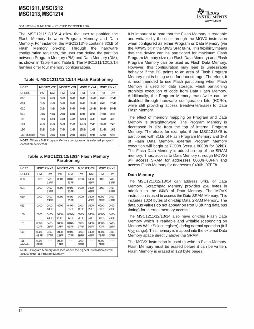
SBAS323G − JUNE 2004 − REVISED OCTOBER 2007
www.ti.com
34
The MSC1211/12/13/14 allow the user to partition theFlash Memory between Program Memory and DataMemory. For instance, the MSC1213Y5 contains 32kB ofFlash Memory on-chip. Through the hardwareconfiguration registers, the user can define the partitionbetween Program Memory (PM) and Data Memory (DM),as shown in Table 4 and Table 5. The MSC1211/12/13/14families offer four memory configurations.
Table 4. MSC1211/12/13/14 Flash Partitioning
HCR0 MSC121xY2 MSC121xY3 MSC121xY4 MSC121xY5
DFSEL PM DM PM DM PM DM PM DM
000 0kB 4kB 0kB 8kB 0kB 16kB 0kB 32kB
001 0kB 4kB 0kB 8kB 0kB 16kB 0kB 32kB
010 0kB 4kB 0kB 8kB 0kB 16kB 16kB 16kB
011 0kB 4kB 0kB 8kB 8kB 8kB 24kB 8kB
100 0kB 4kB 4kB 4kB 12kB 4kB 28kB 4kB
101 2kB 2kB 6kB 2kB 14kB 2kB 30kB 2kB
110 3kB 1kB 7kB 1kB 15kB 1kB 31kB 1kB
111 (default) 4kB 0kB 8kB 0kB 16kB 0kB 32kB 0kB
NOTE: When a 0kB Program Memory configuration is selected, programexecution is external.
Table 5. MSC1211/12/13/14 Flash MemoryPartitioning
HCR0 MSC121xY2 MSC121xY3 MSC121xY4 MSC121xY5
DFSEL PM DM PM DM PM DM PM DM
000 0000 0400-13FF
0000 0400-23FF
0000 0400-43FF
0000 0400-83FF
001 0000 0400-13FF
0000 0400-23FF
0000 0400-43FF
0000 0400-83FF
010 0000 0400-13FF
0000 0400-23FF
0000 0400-43FF
0000-3FFF
0400-43FF
011 0000 0400-13FF
0000 0400-23FF
0000-1FFF
0400-23FF
0000-5FFF
0400-23FF
100 0000 0400-13FF
0000-0FFF
0400-13FF
0000-2FFF
0400-13FF
0000-6FFF
0400-13FF
101 0000-07FF
0400-0BFF
0000-17FF
0400-0BFF
0000-37FF
0400-0BFF
0000-77FF
0400-0BFF
110 0000-0BFF
0400-07FF
0000-1BFF
0400-07FF
0000-3BFF
0400-07FF
0000-7BFF
0400-07FF
111(default)
0000-0FFF
− − 0000-1FFF
− − 0000-3FFF
− − 0000-7FFF
− −
NOTE: Program Memory accesses above the highest listed address willaccess external Program Memory.
It is important to note that the Flash Memory is readableand writable by the user through the MOVX instructionwhen configured as either Program or Data Memory (viathe MXWS bit in the MWS SFR 8Fh). This flexibility meansthat the device can be partitioned for maximum FlashProgram Memory size (no Flash Data Memory) and FlashProgram Memory can be used as Flash Data Memory.However, this configuration may lead to undesirablebehavior if the PC points to an area of Flash ProgramMemory that is being used for data storage. Therefore, itis recommended to use Flash partitioning when FlashMemory is used for data storage. Flash partitioningprohibits execution of code from Data Flash Memory.Additionally, the Program Memory erase/write can bedisabled through hardware configuration bits (HCR0),while still providing access (read/write/erase) to DataFlash Memory.
The effect of memory mapping on Program and DataMemory is straightforward. The Program Memory isdecreased in size from the top of internal ProgramMemory. Therefore, for example, if the MSC1213Y5 ispartitioned with 31kB of Flash Program Memory and 1kBof Flash Data Memory, external Program Memoryexecution will begin at 7C00h (versus 8000h for 32kB).The Flash Data Memory is added on top of the SRAMmemory. Thus, access to Data Memory (through MOVX)will access SRAM for addresses 0000h−03FFh andaccess Flash Memory for addresses 0400h−07FFh.
Data Memory
The MSC1211/12/13/14 can address 64kB of DataMemory. Scratchpad Memory provides 256 bytes inaddition to the 64kB of Data Memory. The MOVXinstruction is used to access the Data SRAM Memory. Thisincludes 1024 bytes of on-chip Data SRAM Memory. Thedata bus values do not appear on Port 0 (during data bustiming) for internal memory access.
The MSC1211/12/13/14 also have on-chip Flash DataMemory which is readable and writable (depending onMemory Write Select register) during normal operation (fullVDD range). This memory is mapped into the external DataMemory space directly above the SRAM.
The MOVX instruction is used to write to Flash Memory.Flash Memory must be erased before it can be written.Flash Memory is erased in 128 byte pages.
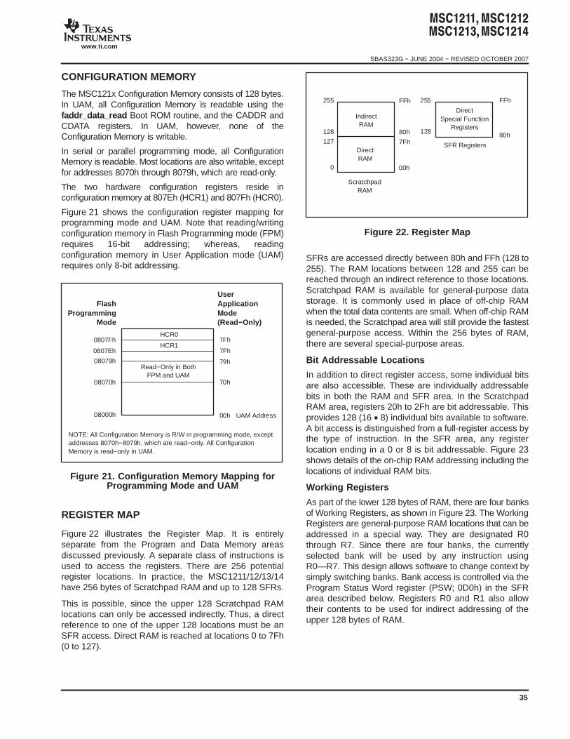
SBAS323G − JUNE 2004 − REVISED OCTOBER 2007
www.ti.com
35
CONFIGURATION MEMORY
The MSC121x Configuration Memory consists of 128 bytes.In UAM, all Configuration Memory is readable using thefaddr_data_read Boot ROM routine, and the CADDR andCDATA registers. In UAM, however, none of theConfiguration Memory is writable.
In serial or parallel programming mode, all ConfigurationMemory is readable. Most locations are also writable, exceptfor addresses 8070h through 8079h, which are read-only.
The two hardware configuration registers reside inconfiguration memory at 807Eh (HCR1) and 807Fh (HCR0).
Figure 21 shows the configuration register mapping forprogramming mode and UAM. Note that reading/writingconfiguration memory in Flash Programming mode (FPM)requires 16-bit addressing; whereas, readingconfiguration memory in User Application mode (UAM)requires only 8-bit addressing.
Read−Only in BothFPM and UAM
00h UAM Address
HCR0
HCR17Fh
79h
70h
7Fh0807Fh
0807Eh
08079h
08070h
08000h
FlashProgramming
Mode
UserApplicationMode(Read−Only)
NOTE: All Configuration Memory is R/W in programming mode, exceptaddresses 8070h−8079h, which are read−only. All ConfigurationMemory is read−only in UAM.
Figure 21. Configuration Memory Mapping forProgramming Mode and UAM
REGISTER MAP
Figure 22 illustrates the Register Map. It is entirelyseparate from the Program and Data Memory areasdiscussed previously. A separate class of instructions isused to access the registers. There are 256 potentialregister locations. In practice, the MSC1211/12/13/14have 256 bytes of Scratchpad RAM and up to 128 SFRs.
This is possible, since the upper 128 Scratchpad RAMlocations can only be accessed indirectly. Thus, a directreference to one of the upper 128 locations must be anSFR access. Direct RAM is reached at locations 0 to 7Fh(0 to 127).
FFh 255
128
FFh
80h80h
7Fh
00h
IndirectRAM
DirectRAM
ScratchpadRAM
SFR Registers
DirectSpecial Function
Registers
255
128
127
0
Figure 22. Register Map
SFRs are accessed directly between 80h and FFh (128 to255). The RAM locations between 128 and 255 can bereached through an indirect reference to those locations.Scratchpad RAM is available for general-purpose datastorage. It is commonly used in place of off-chip RAMwhen the total data contents are small. When off-chip RAMis needed, the Scratchpad area will still provide the fastestgeneral-purpose access. Within the 256 bytes of RAM,there are several special-purpose areas.
Bit Addressable Locations
In addition to direct register access, some individual bitsare also accessible. These are individually addressablebits in both the RAM and SFR area. In the ScratchpadRAM area, registers 20h to 2Fh are bit addressable. Thisprovides 128 (16 • 8) individual bits available to software.A bit access is distinguished from a full-register access bythe type of instruction. In the SFR area, any registerlocation ending in a 0 or 8 is bit addressable. Figure 23shows details of the on-chip RAM addressing including thelocations of individual RAM bits.
Working Registers
As part of the lower 128 bytes of RAM, there are four banksof Working Registers, as shown in Figure 23. The WorkingRegisters are general-purpose RAM locations that can beaddressed in a special way. They are designated R0through R7. Since there are four banks, the currentlyselected bank will be used by any instruction usingR0—R7. This design allows software to change context bysimply switching banks. Bank access is controlled via theProgram Status Word register (PSW; 0D0h) in the SFRarea described below. Registers R0 and R1 also allowtheir contents to be used for indirect addressing of theupper 128 bytes of RAM.
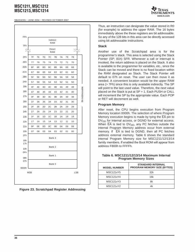
SBAS323G − JUNE 2004 − REVISED OCTOBER 2007
www.ti.com
36
FFh
7Fh
2Fh
2Dh
2Eh
2Ch
2Bh
2Ah
29h
28h
27h
26h
25h
24h
23h
22h
21h
20h
1Fh
18h17h
10h
0Fh
08h07h
7F 7E 7D 7C 7B 7A 79 78
77 76 75 74 73 72 71 70
6F 6E 6D 6C 6B 6A 69 68
67 66 65 64 63 62 61 60
5F 5E 5D 5C 5B 5A 59 58
57 56 55 54 53 52 51 50
4F 4E 4D 4C 4B 4A 49 48
47 46 45 44 43 42 41 40
3F 3E 3D 3C 3B 3A 39 38
37 36 35 34 33 32 31 30
2F 2E 2D 2C 2B 2A 29 28
27 26 25 24 23 22 21 20
1F 1E 1D 1C 1B 1A 19 18
17 16 15 14 13 12 11 10
0F 0E 0D 0C 0B 0A 09 08
07 06 05 04 03 02 01 00
0000h
DirectRAM
Bank 3
Bit-
Add
ress
able
Bank 2
Bank 1
Bank 0
MSB LSB
IndirectRAM
Figure 23. Scratchpad Register Addressing
Thus, an instruction can designate the value stored in R0(for example) to address the upper RAM. The 16 bytesimmediately above the these registers are bit addressable.So any of the 128 bits in this area can be directly accessedusing bit addressable instructions.
Stack
Another use of the Scratchpad area is for theprogrammer’s stack. This area is selected using the StackPointer (SP; 81h) SFR. Whenever a call or interrupt isinvoked, the return address is placed on the Stack. It alsois available to the programmer for variables, etc., since theStack can be moved and there is no fixed location withinthe RAM designated as Stack. The Stack Pointer willdefault to 07h on reset. The user can then move it asneeded. A convenient location would be the upper RAMarea (> 7Fh) since this is only available indirectly. The SPwill point to the last used value. Therefore, the next valueplaced on the Stack is put at SP + 1. Each PUSH or CALLwill increment the SP by the appropriate value. Each POPor RET will decrement as well.
Program Memory
After reset, the CPU begins execution from ProgramMemory location 0000h. The selection of where ProgramMemory execution begins is made by tying the EA pin toDVDD for internal access, or DGND for external access.When EA is tied to DVDD, any PC fetches outside theinternal Program Memory address occur from externalmemory. If EA is tied to DGND, then all PC fetchesaddress external memory. Table 6 shows the standardinternal Program Memory size for MSC1211/12/13/14family members. If enabled the Boot ROM will appear fromaddress F800h to FFFFh.
Table 6. MSC1211/12/13/14 Maximum InternalProgram Memory Sizes
MODEL NUMBERSTANDARD INTERNAL
PROGRAM MEMORY SIZE (BYTES)
MSC121xY5 32k
MSC121xY4 16k
MSC121xY3 8k
MSC121xY2 4k

SBAS323G − JUNE 2004 − REVISED OCTOBER 2007
www.ti.com
37
ACCESSING EXTERNAL MEMORY
If external memory is used, P0 and P2 must be configuredas address and data lines. If external memory is not used, P0and P2 can be configured as general-purpose I/O linesthrough the hardware configuration register (HCR0, HCR1).
To enable access to external memory, bits 0 and 1 of theHCR1 register must be set to ‘0’. When these bits areenabled all memory accesses for both internal andexternal memory will appear on Ports 0 and 2. During thedata portion of the cycle for internal memory, Port 0 will bezero for security purposes.
Accesses to external memory are of two types: to externalProgram Memory and to external Data Memory. Accessesto external Program Memory use signal PSEN (programstore enable) as the read strobe. Accesses to externalData Memory use RD or WR (alternate functions of P3.7and P3.6) to strobe the memory.
If desired, External Program Memory and external DataMemory may be combined by applying the RD and PSENsignals to the inputs of an AND gate and using the outputof the gate as the read strobe to the external Program/DataMemory.
A program fetch from external Program Memory uses a16-bit address. Accesses to external Data Memory canuse either a 16-bit address (MOVX @DPTR) or an 8-bitaddress (MOVX @RI).
If Port 2 is selected for external memory use (HCR1, bit 0),it cannot be used as general-purpose I/O. This bit (or Bit1 of HCR1) also forces bits P3.6 and P3.7 to be used forWR and RD instead of I/O. Port 2, P3.6, and P3.7 shouldall be written to ‘1.’
If an 8-bit address is being used (MOVX @RI), the contentsof the MPAGE (92h) SFR remain at the Port 2 pinsthroughout the external memory cycle, which facilitatespaging.
In any case, the low byte of the address is time-multiplexedwith the data byte on Port 0. The ADDR/DATA signals useCMOS drivers in the Port 0, Port 2, WR, and RD outputbuffers. Thus, in this application, the Port 0 pins are notopen-drain outputs, and do not require external pull-ups forhigh-speed access. Signal ALE (Address Latch Enable)should be used to capture the address byte into an externallatch. The address byte is valid at the negative transitionof ALE. Then, in a write cycle, the data byte to be writtenappears on Port 0 just before WR is activated, and remainsthere until after WR is deactivated. In a read cycle, theincoming byte is accepted at Port 0 just before the readstrobe is deactivated.
The functions of Port 0 and Port 2 are selected in HCR1.(Hardware configuration registers can only be changedduring Flash Programming mode.) The default state is forPort 0 and Port 2 to be used as general-purpose I/O. If anexternal memory access is attempted when they areconfigured as general-purpose I/O, the values of Port 0and Port 2 will not be affected.
External Program Memory is accessed under two conditions:
1. Whenever signal EA is low during reset, then all futurecode and data accesses are external; or
2. Whenever the Program Counter (PC) contains anumber that is outside of the internal Program Memoryaddress range, if the ports are enabled.
If Port 0 and Port 2 are selected for external memory, all 8bits of Port 0 and Port 2, as well as P3.6 and P3.7, arededicated to an output function and may not be used forgeneral-purpose I/O. During external program fetches,Port 2 outputs the high byte of the PC.
Programming Flash Memory
There are four sections of Flash Memory for programming:
1. 128 configuration bytes.
2. Reset sector (4kB) (not to be confused with the 2kBBoot ROM).
3. Program Memory.
4. Data Memory.
Boot ROM
There is a 2kB Boot ROM that controls operation duringserial or parallel programming. Additionally, the Boot ROMroutines can be accessed during the user mode if it isenabled. When enabled, the Boot ROM routines will belocated at memory addresses F800h−FFFFh during usermode. In program mode the Boot ROM is located in the first2kB of Program Memory. For additional information, referto Application Note SBAA085, available for download fromthe TI web site (www.ti.com).
The MSC1211/12/13/14 are shipped with Flash Memoryerased (all 1s). Parallel programming methods typicallyinvolve a third-party programmer. Serial programmingmethods typically involve in-system programming. UAMallows Code Program and Data Memory programming.The actual code for Flash programming cannot executefrom Flash. That code must execute from the Boot ROMor internal (von Neumann) RAM.
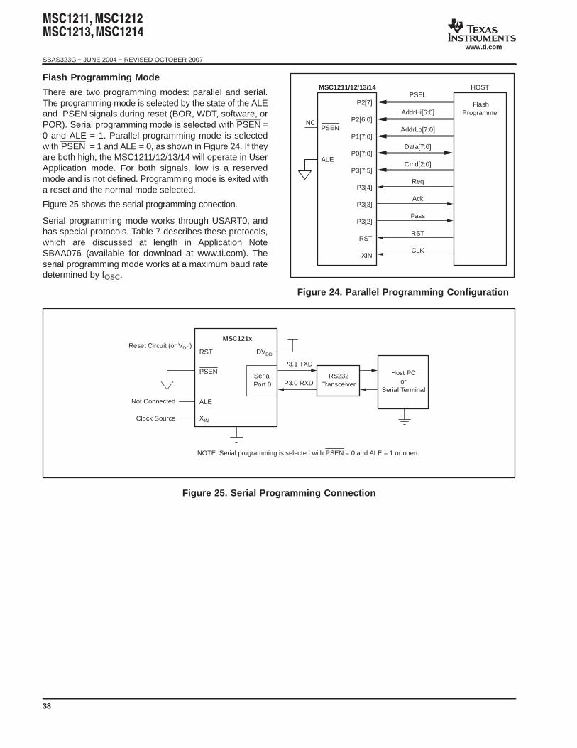
SBAS323G − JUNE 2004 − REVISED OCTOBER 2007
www.ti.com
38
Flash Programming Mode
There are two programming modes: parallel and serial.The programming mode is selected by the state of the ALEand PSEN signals during reset (BOR, WDT, software, orPOR). Serial programming mode is selected with PSEN =0 and ALE = 1. Parallel programming mode is selectedwith PSEN = 1 and ALE = 0, as shown in Figure 24. If theyare both high, the MSC1211/12/13/14 will operate in UserApplication mode. For both signals, low is a reservedmode and is not defined. Programming mode is exited witha reset and the normal mode selected.
Figure 25 shows the serial programming conection.
Serial programming mode works through USART0, andhas special protocols. Table 7 describes these protocols,which are discussed at length in Application NoteSBAA076 (available for download at www.ti.com). Theserial programming mode works at a maximum baud ratedetermined by fOSC.
PSEN
ALE
MSC1211/12/13/14 HOST
FlashProgrammer
P2[7]
P2[6:0]
P1[7:0]
P0[7:0]
P3[7:5]
P3[4]
P3[3]
P3[2]
RST
XIN
PSEL
AddrHi[6:0]
AddrLo[7:0]
Data[7:0]
Cmd[2:0]
Req
Ack
Pass
RST
CLK
NC
Figure 24. Parallel Programming Configuration
MSC121x
PSEN
P3.0 RXD
P3.1 TXD
SerialPort 0
ALE
RST DVDD
XIN
Reset Circuit (or VDD)
Clock Source
Not Connected
RS232Transceiver
Host PCor
Serial Terminal
NOTE: Serial programming is selected with PSEN = 0 and ALE = 1 or open.
Figure 25. Serial Programming Connection
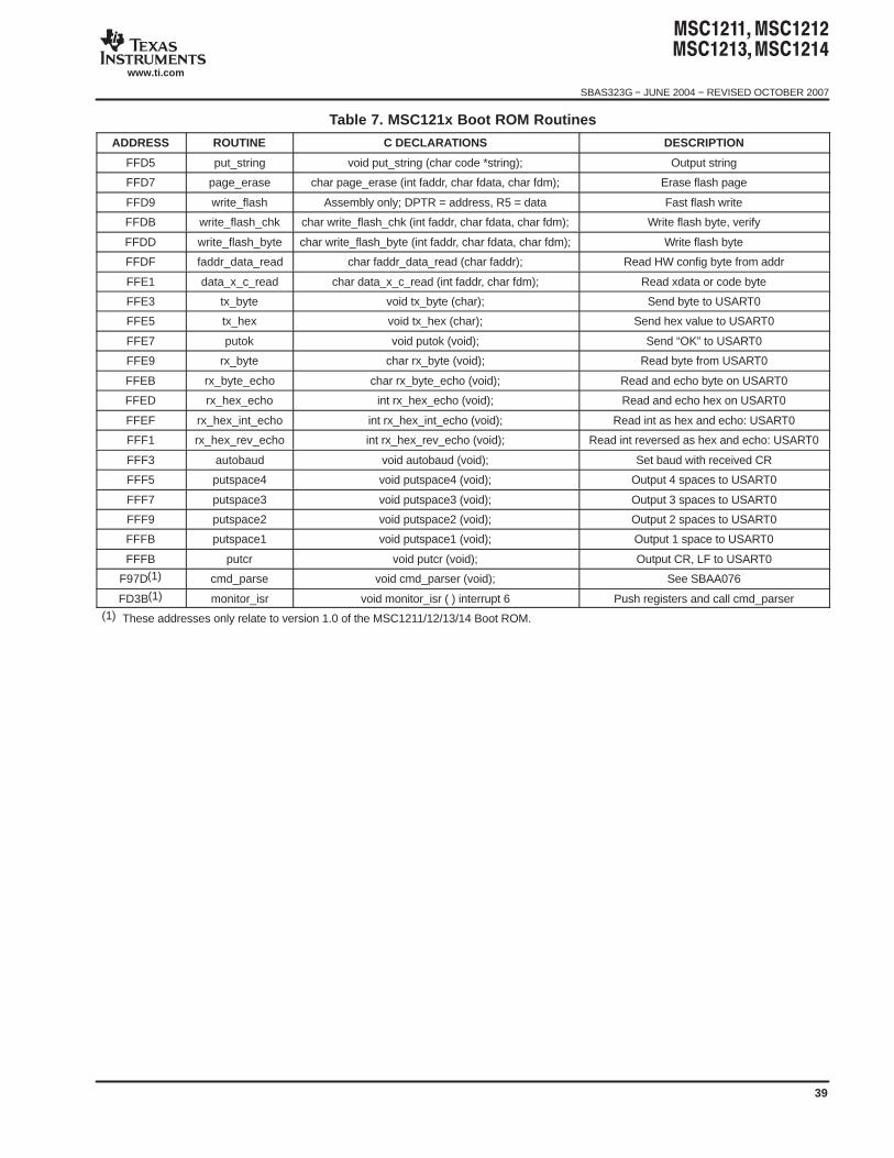
SBAS323G − JUNE 2004 − REVISED OCTOBER 2007
www.ti.com
39
Table 7. MSC121x Boot ROM Routines
ADDRESS ROUTINE C DECLARATIONS DESCRIPTION
FFD5 put_string void put_string (char code *string); Output string
FFD7 page_erase char page_erase (int faddr, char fdata, char fdm); Erase flash page
FFD9 write_flash Assembly only; DPTR = address, R5 = data Fast flash write
FFDB write_flash_chk char write_flash_chk (int faddr, char fdata, char fdm); Write flash byte, verify
FFDD write_flash_byte char write_flash_byte (int faddr, char fdata, char fdm); Write flash byte
FFDF faddr_data_read char faddr_data_read (char faddr); Read HW config byte from addr
FFE1 data_x_c_read char data_x_c_read (int faddr, char fdm); Read xdata or code byte
FFE3 tx_byte void tx_byte (char); Send byte to USART0
FFE5 tx_hex void tx_hex (char); Send hex value to USART0
FFE7 putok void putok (void); Send “OK” to USART0
FFE9 rx_byte char rx_byte (void); Read byte from USART0
FFEB rx_byte_echo char rx_byte_echo (void); Read and echo byte on USART0
FFED rx_hex_echo int rx_hex_echo (void); Read and echo hex on USART0
FFEF rx_hex_int_echo int rx_hex_int_echo (void); Read int as hex and echo: USART0
FFF1 rx_hex_rev_echo int rx_hex_rev_echo (void); Read int reversed as hex and echo: USART0
FFF3 autobaud void autobaud (void); Set baud with received CR
FFF5 putspace4 void putspace4 (void); Output 4 spaces to USART0
FFF7 putspace3 void putspace3 (void); Output 3 spaces to USART0
FFF9 putspace2 void putspace2 (void); Output 2 spaces to USART0
FFFB putspace1 void putspace1 (void); Output 1 space to USART0
FFFB putcr void putcr (void); Output CR, LF to USART0
F97D(1) cmd_parse void cmd_parser (void); See SBAA076
FD3B(1) monitor_isr void monitor_isr ( ) interrupt 6 Push registers and call cmd_parser(1) These addresses only relate to version 1.0 of the MSC1211/12/13/14 Boot ROM.
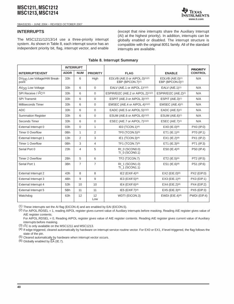
SBAS323G − JUNE 2004 − REVISED OCTOBER 2007
www.ti.com
40
INTERRUPTS
The MSC1211/12/13/14 use a three-priority interruptsystem. As shown in Table 8, each interrupt source has anindependent priority bit, flag, interrupt vector, and enable
(except that nine interrupts share the Auxiliary Interrupt(AI) at the highest priority). In addition, interrupts can beglobally enabled or disabled. The interrupt structure iscompatible with the original 8051 family. All of the standardinterrupts are available.
Table 8. Interrupt Summary
INTERRUPTPRIORITY
INTERRUPT/EVENT ADDR NUM PRIORITY FLAG ENABLEPRIORITYCONTROL
DVDD Low Voltage/HW Break-point
33h 6 High EDLVB (AIE.0 or AIPOL.0)(1)(2)
EBP (BPCON.7)(1)EDLVB (AIE.0)(1)
EBP (BPCON.0)(1)N/A
AVDD Low Voltage 33h 6 0 EALV (AIE.1 or AIPOL.1)(1)(2) EALV (AIE.1)(1) N/A
SPI Receive / I2C(3) 33h 6 0 ESPIR/EI2C (AIE.2 or AIPOL.2)(1)(2) ESPIR/EI2C (AIE.2)(1) N/A
SPI Transmit 33h 6 0 ESPIT (AIE.3 or AIPOL.3)(1)(2) ESPIT (AIE.3)(1) N/A
Milliseconds Timer 33h 6 0 EMSEC (AIE.4 or AIPOL.4)(1)(2) EMSEC (AIE.4)(1) N/A
ADC 33h 6 0 EADC (AIE.5 or AIPOL.5)(1)(2) EADC (AIE.5)(1) N/A
Summation Register 33h 6 0 ESUM (AIE.6 or AIPOL.6)(1)(2) ESUM (AIE.6)(1) N/A
Seconds Timer 33h 6 0 ESEC (AIE.7 or AIPOL.7)(1)(2) ESEC (AIE.7)(1) N/A
External Interrupt 0 03h 0 1 IE0 (TCON.1)(4) EX0 (IE.0)(6) PX0 (IP.0)
Timer 0 Overflow 0Bh 1 2 TF0 (TCON.5)(5) ET1 (IE.1)(6) PT0 (IP.1)
External Interrupt 1 13h 2 3 IE1 (TCON.3)(4) EX1 (IE.2)(6) PX1 (IP.2)
Timer 1 Overflow 0Bh 3 4 TF1 (TCON.7)(5) ET1 (IE.3)(6) PT1 (IP.3)
Serial Port 0 23h 4 5 RI_0 (SCON0.0)TI_0 (SCON0.1)
ES0 (IE.4)(6) PS0 (IP.4)
Timer 2 Overflow 2Bh 5 6 TF2 (T2CON.7) ET2 (IE.5)(6) PT2 (IP.5)
Serial Port 1 3Bh 7 7 RI_1 (SCON1.0)TI_1 (SCON1.1)
ES1 (IE.6)(6) PS1 (IP.6)
External Interrupt 2 43h 8 8 IE2 (EXIF.4)(4) EX2 (EIE.0)(6) PX2 (EIP.0)
External Interrupt 3 4Bh 9 9 IE3 (EXIF.5)(4) EX3 (EIE.1)(6) PX3 (EIP.1)
External Interrupt 4 53h 10 10 IE4 (EXIF.6)(4) EX4 (EIE.2)(6) PX4 (EIP.2)
External Interrupt 5 5Bh 11 11 IE5 (EXIF.7)(4) EX5 (EIE.3)(6) PX5 (EIP.3)
Watchdog 63h 12 12Low
WDTI (EICON.3) EWDI (EIE.4)(6) PWDI (EIP.4)
(1) These interrupts set the AI flag (EICON.4) and are enabled by EAI (EICON.5).(2) For AIPOL.RDSEL = 1, reading AIPOL register gives current value of Auxiliary interrupts before masking. Reading AIE register gives value of
AIE register contents.For AIPOL.RDSEL = 0, Reading AIPOL register gives value of AIE register contents. Reading AIE register gives current value of Auxiliaryinterrupts before masking.
(3) I2C is only available on the MSC1211 and MSC1213.(4) If edge-triggered, cleared automatically by hardware on interrupt service routine vector. For EX0 or EX1, if level-triggered, the flag follows the
state of the pin.(5) Cleared automatically by hardware when interrupt vector occurs.(6) Globally enabled by EA (IE.7).
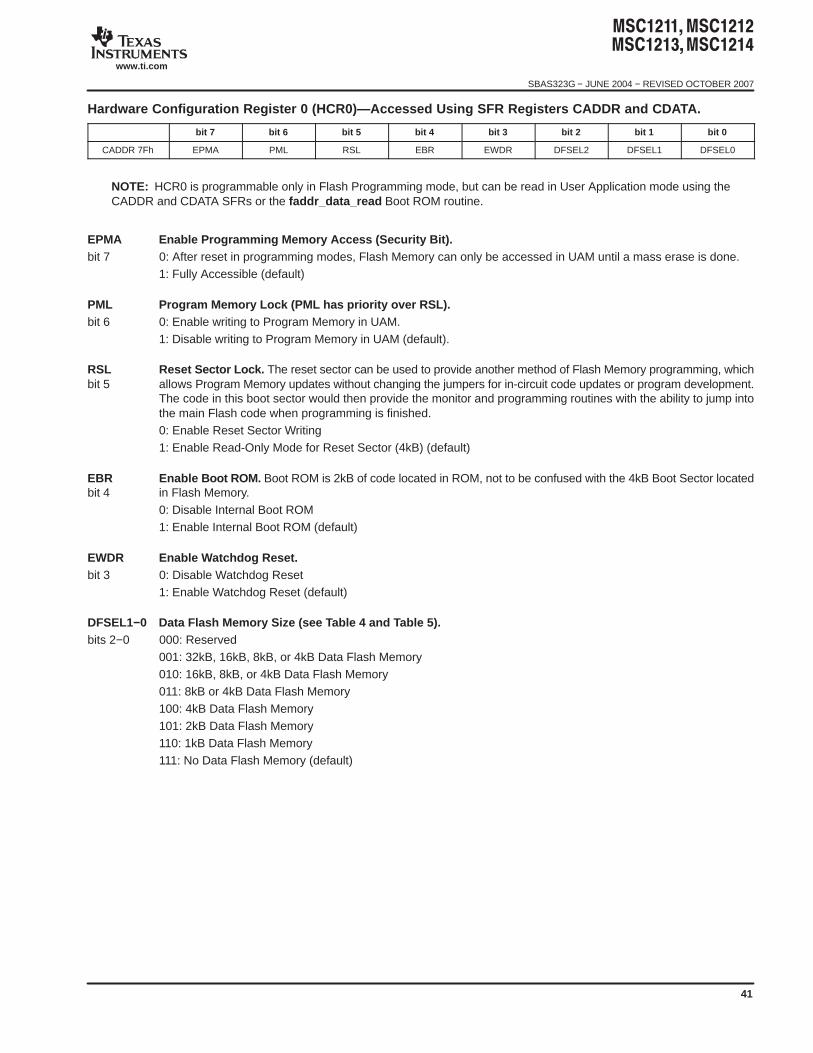
SBAS323G − JUNE 2004 − REVISED OCTOBER 2007
www.ti.com
41
Hardware Configuration Register 0 (HCR0)—Accessed Using SFR Registers CADDR and CDATA.
bit 7 bit 6 bit 5 bit 4 bit 3 bit 2 bit 1 bit 0
CADDR 7Fh EPMA PML RSL EBR EWDR DFSEL2 DFSEL1 DFSEL0
NOTE: HCR0 is programmable only in Flash Programming mode, but can be read in User Application mode using theCADDR and CDATA SFRs or the faddr_data_read Boot ROM routine.
EPMA Enable Programming Memory Access (Security Bit).bit 7 0: After reset in programming modes, Flash Memory can only be accessed in UAM until a mass erase is done.
1: Fully Accessible (default)
PML Program Memory Lock (PML has priority over RSL).bit 6 0: Enable writing to Program Memory in UAM.
1: Disable writing to Program Memory in UAM (default).
RSL Reset Sector Lock. The reset sector can be used to provide another method of Flash Memory programming, whichbit 5 allows Program Memory updates without changing the jumpers for in-circuit code updates or program development.
The code in this boot sector would then provide the monitor and programming routines with the ability to jump intothe main Flash code when programming is finished.0: Enable Reset Sector Writing1: Enable Read-Only Mode for Reset Sector (4kB) (default)
EBR Enable Boot ROM. Boot ROM is 2kB of code located in ROM, not to be confused with the 4kB Boot Sector locatedbit 4 in Flash Memory.
0: Disable Internal Boot ROM1: Enable Internal Boot ROM (default)
EWDR Enable Watchdog Reset.bit 3 0: Disable Watchdog Reset
1: Enable Watchdog Reset (default)
DFSEL1−0 Data Flash Memory Size (see Table 4 and Table 5).bits 2−0 000: Reserved
001: 32kB, 16kB, 8kB, or 4kB Data Flash Memory010: 16kB, 8kB, or 4kB Data Flash Memory011: 8kB or 4kB Data Flash Memory100: 4kB Data Flash Memory101: 2kB Data Flash Memory110: 1kB Data Flash Memory111: No Data Flash Memory (default)
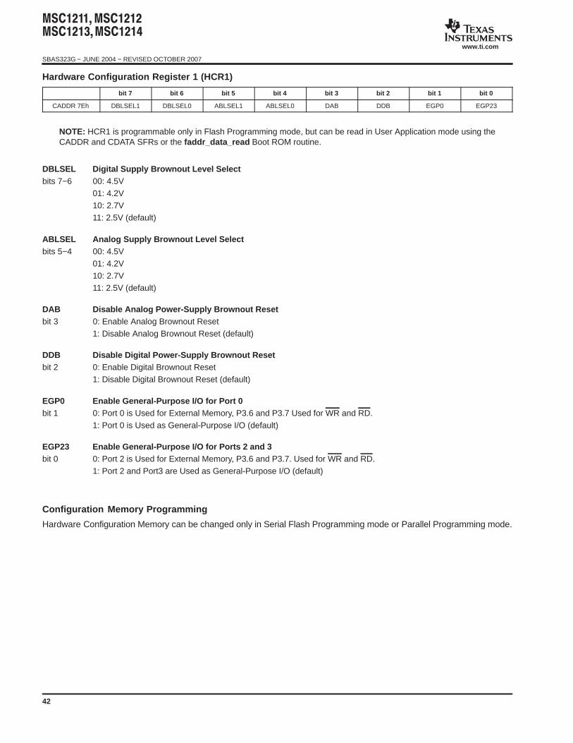
SBAS323G − JUNE 2004 − REVISED OCTOBER 2007
www.ti.com
42
Hardware Configuration Register 1 (HCR1)
bit 7 bit 6 bit 5 bit 4 bit 3 bit 2 bit 1 bit 0
CADDR 7Eh DBLSEL1 DBLSEL0 ABLSEL1 ABLSEL0 DAB DDB EGP0 EGP23
NOTE: HCR1 is programmable only in Flash Programming mode, but can be read in User Application mode using theCADDR and CDATA SFRs or the faddr_data_read Boot ROM routine.
DBLSEL Digital Supply Brownout Level Selectbits 7−6 00: 4.5V
01: 4.2V10: 2.7V11: 2.5V (default)
ABLSEL Analog Supply Brownout Level Selectbits 5−4 00: 4.5V
01: 4.2V10: 2.7V11: 2.5V (default)
DAB Disable Analog Power-Supply Brownout Resetbit 3 0: Enable Analog Brownout Reset
1: Disable Analog Brownout Reset (default)
DDB Disable Digital Power-Supply Brownout Resetbit 2 0: Enable Digital Brownout Reset
1: Disable Digital Brownout Reset (default)
EGP0 Enable General-Purpose I/O for Port 0bit 1 0: Port 0 is Used for External Memory, P3.6 and P3.7 Used for WR and RD.
1: Port 0 is Used as General-Purpose I/O (default)
EGP23 Enable General-Purpose I/O for Ports 2 and 3bit 0 0: Port 2 is Used for External Memory, P3.6 and P3.7. Used for WR and RD.
1: Port 2 and Port3 are Used as General-Purpose I/O (default)
Configuration Memory Programming
Hardware Configuration Memory can be changed only in Serial Flash Programming mode or Parallel Programming mode.
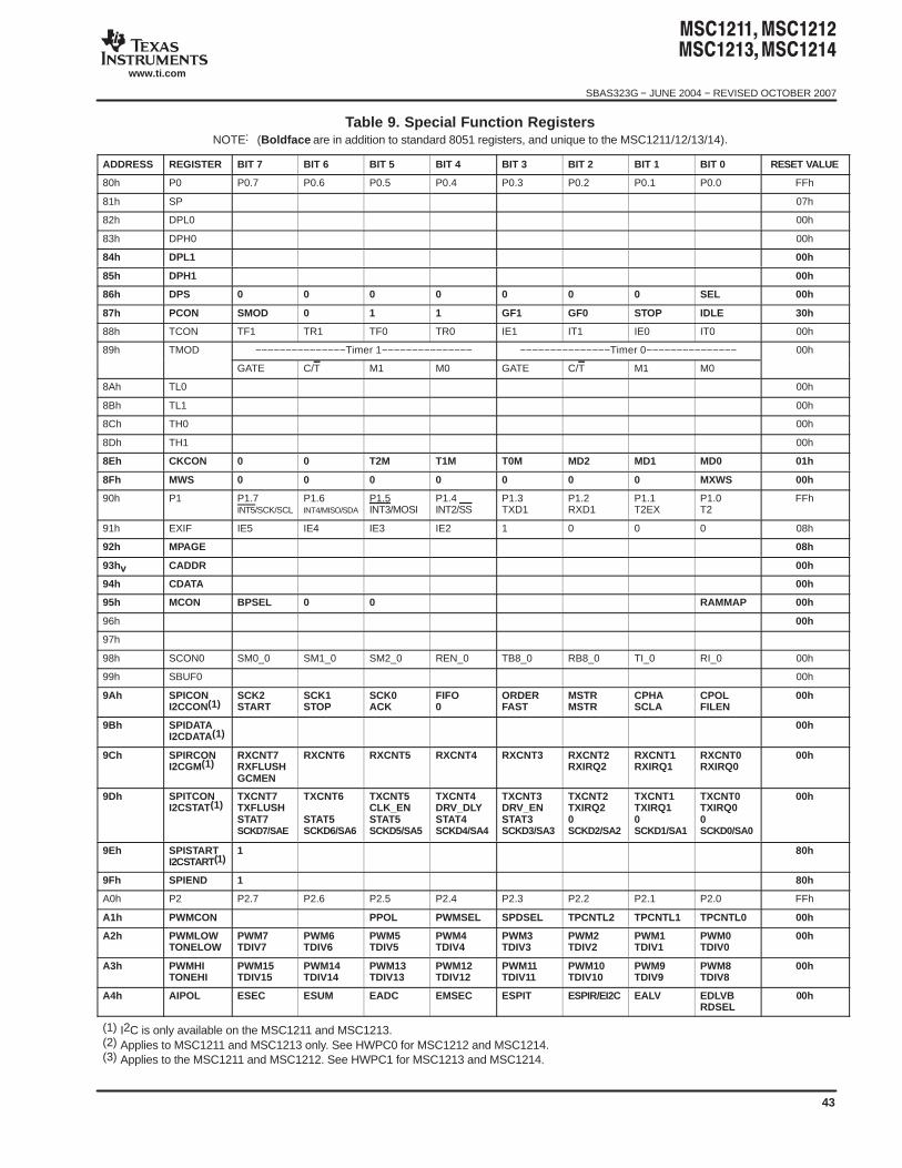
SBAS323G − JUNE 2004 − REVISED OCTOBER 2007
www.ti.com
43
Table 9. Special Function Registers NOTE: (Boldface are in addition to standard 8051 registers, and unique to the MSC1211/12/13/14).
ADDRESS REGISTER BIT 7 BIT 6 BIT 5 BIT 4 BIT 3 BIT 2 BIT 1 BIT 0 RESET VALUE
80h P0 P0.7 P0.6 P0.5 P0.4 P0.3 P0.2 P0.1 P0.0 FFh
81h SP 07h
82h DPL0 00h
83h DPH0 00h
84h DPL1 00h
85h DPH1 00h
86h DPS 0 0 0 0 0 0 0 SEL 00h
87h PCON SMOD 0 1 1 GF1 GF0 STOP IDLE 30h
88h TCON TF1 TR1 TF0 TR0 IE1 IT1 IE0 IT0 00h
89h TMOD −−−−−−−−−−−−−−−Timer 1−−−−−−−−−−−−−−− −−−−−−−−−−−−−−−Timer 0−−−−−−−−−−−−−−− 00h89h TMOD
GATE C/T M1 M0 GATE C/T M1 M0
00h
8Ah TL0 00h
8Bh TL1 00h
8Ch TH0 00h
8Dh TH1 00h
8Eh CKCON 0 0 T2M T1M T0M MD2 MD1 MD0 01h
8Fh MWS 0 0 0 0 0 0 0 MXWS 00h
90h P1 P1.7INT5/SCK/SCL
P1.6INT4/MISO/SDA
P1.5INT3/MOSI
P1.4INT2/SS
P1.3TXD1
P1.2RXD1
P1.1T2EX
P1.0T2
FFh
91h EXIF IE5 IE4 IE3 IE2 1 0 0 0 08h
92h MPAGE 08h
93hv CADDR 00h
94h CDATA 00h
95h MCON BPSEL 0 0 RAMMAP 00h
96h 00h
97h
98h SCON0 SM0_0 SM1_0 SM2_0 REN_0 TB8_0 RB8_0 TI_0 RI_0 00h
99h SBUF0 00h
9Ah SPICONI2CCON(1)
SCK2START
SCK1STOP
SCK0ACK
FIFO0
ORDERFAST
MSTRMSTR
CPHASCLA
CPOLFILEN
00h
9Bh SPIDATAI2CDATA(1)
00h
9Ch SPIRCONI2CGM(1)
RXCNT7RXFLUSHGCMEN
RXCNT6 RXCNT5 RXCNT4 RXCNT3 RXCNT2RXIRQ2
RXCNT1RXIRQ1
RXCNT0RXIRQ0
00h
9Dh SPITCONI2CSTAT(1)
TXCNT7TXFLUSHSTAT7SCKD7/SAE
TXCNT6
STAT5SCKD6/SA6
TXCNT5CLK_ENSTAT5SCKD5/SA5
TXCNT4DRV_DLYSTAT4SCKD4/SA4
TXCNT3DRV_ENSTAT3SCKD3/SA3
TXCNT2TXIRQ20SCKD2/SA2
TXCNT1TXIRQ10SCKD1/SA1
TXCNT0TXIRQ00SCKD0/SA0
00h
9Eh SPISTARTI2CSTART(1)
1 80h
9Fh SPIEND 1 80h
A0h P2 P2.7 P2.6 P2.5 P2.4 P2.3 P2.2 P2.1 P2.0 FFh
A1h PWMCON PPOL PWMSEL SPDSEL TPCNTL2 TPCNTL1 TPCNTL0 00h
A2h PWMLOWTONELOW
PWM7TDIV7
PWM6TDIV6
PWM5TDIV5
PWM4TDIV4
PWM3TDIV3
PWM2TDIV2
PWM1TDIV1
PWM0TDIV0
00h
A3h PWMHITONEHI
PWM15TDIV15
PWM14TDIV14
PWM13TDIV13
PWM12TDIV12
PWM11TDIV11
PWM10TDIV10
PWM9TDIV9
PWM8TDIV8
00h
A4h AIPOL ESEC ESUM EADC EMSEC ESPIT ESPIR/EI2C EALV EDLVBRDSEL
00h
(1) I2C is only available on the MSC1211 and MSC1213.(2) Applies to MSC1211 and MSC1213 only. See HWPC0 for MSC1212 and MSC1214.(3) Applies to the MSC1211 and MSC1212. See HWPC1 for MSC1213 and MSC1214.
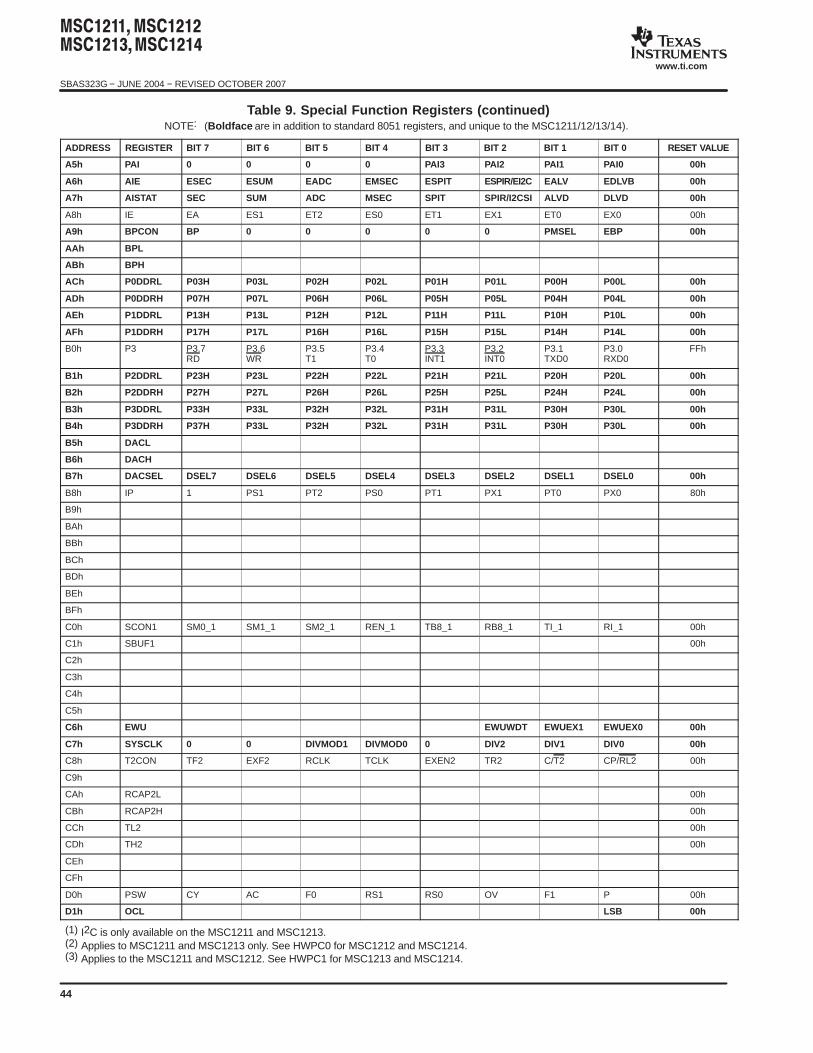
SBAS323G − JUNE 2004 − REVISED OCTOBER 2007
www.ti.com
44
Table 9. Special Function Registers (continued)NOTE: (Boldface are in addition to standard 8051 registers, and unique to the MSC1211/12/13/14).
ADDRESS RESET VALUEBIT 0BIT 1BIT 2BIT 3BIT 4BIT 5BIT 6BIT 7REGISTER
A5h PAI 0 0 0 0 PAI3 PAI2 PAI1 PAI0 00h
A6h AIE ESEC ESUM EADC EMSEC ESPIT ESPIR/EI2C EALV EDLVB 00h
A7h AISTAT SEC SUM ADC MSEC SPIT SPIR/I2CSI ALVD DLVD 00h
A8h IE EA ES1 ET2 ES0 ET1 EX1 ET0 EX0 00h
A9h BPCON BP 0 0 0 0 0 PMSEL EBP 00h
AAh BPL
ABh BPH
ACh P0DDRL P03H P03L P02H P02L P01H P01L P00H P00L 00h
ADh P0DDRH P07H P07L P06H P06L P05H P05L P04H P04L 00h
AEh P1DDRL P13H P13L P12H P12L P11H P11L P10H P10L 00h
AFh P1DDRH P17H P17L P16H P16L P15H P15L P14H P14L 00h
B0h P3 P3.7RD
P3.6WR
P3.5T1
P3.4T0
P3.3INT1
P3.2INT0
P3.1TXD0
P3.0RXD0
FFh
B1h P2DDRL P23H P23L P22H P22L P21H P21L P20H P20L 00h
B2h P2DDRH P27H P27L P26H P26L P25H P25L P24H P24L 00h
B3h P3DDRL P33H P33L P32H P32L P31H P31L P30H P30L 00h
B4h P3DDRH P37H P33L P32H P32L P31H P31L P30H P30L 00h
B5h DACL
B6h DACH
B7h DACSEL DSEL7 DSEL6 DSEL5 DSEL4 DSEL3 DSEL2 DSEL1 DSEL0 00h
B8h IP 1 PS1 PT2 PS0 PT1 PX1 PT0 PX0 80h
B9h
BAh
BBh
BCh
BDh
BEh
BFh
C0h SCON1 SM0_1 SM1_1 SM2_1 REN_1 TB8_1 RB8_1 TI_1 RI_1 00h
C1h SBUF1 00h
C2h
C3h
C4h
C5h
C6h EWU EWUWDT EWUEX1 EWUEX0 00h
C7h SYSCLK 0 0 DIVMOD1 DIVMOD0 0 DIV2 DIV1 DIV0 00h
C8h T2CON TF2 EXF2 RCLK TCLK EXEN2 TR2 C/T2 CP/RL2 00h
C9h
CAh RCAP2L 00h
CBh RCAP2H 00h
CCh TL2 00h
CDh TH2 00h
CEh
CFh
D0h PSW CY AC F0 RS1 RS0 OV F1 P 00h
D1h OCL LSB 00h
(1) I2C is only available on the MSC1211 and MSC1213.(2) Applies to MSC1211 and MSC1213 only. See HWPC0 for MSC1212 and MSC1214.(3) Applies to the MSC1211 and MSC1212. See HWPC1 for MSC1213 and MSC1214.
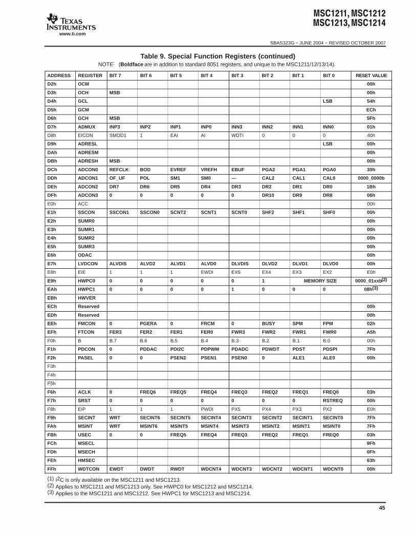
SBAS323G − JUNE 2004 − REVISED OCTOBER 2007
www.ti.com
45
Table 9. Special Function Registers (continued)NOTE: (Boldface are in addition to standard 8051 registers, and unique to the MSC1211/12/13/14).
ADDRESS RESET VALUEBIT 0BIT 1BIT 2BIT 3BIT 4BIT 5BIT 6BIT 7REGISTER
D2h OCM 00h
D3h OCH MSB 00h
D4h GCL LSB 54h
D5h GCM ECh
D6h GCH MSB 5Fh
D7h ADMUX INP3 INP2 INP1 INP0 INN3 INN2 INN1 INN0 01h
D8h EICON SMOD1 1 EAI AI WDTI 0 0 0 40h
D9h ADRESL LSB 00h
DAh ADRESM 00h
DBh ADRESH MSB 00h
DCh ADCON0 REFCLK BOD EVREF VREFH EBUF PGA2 PGA1 PGA0 30h
DDh ADCON1 OF_UF POL SM1 SM0 — CAL2 CAL1 CAL0 0000_0000b
DEh ADCON2 DR7 DR6 DR5 DR4 DR3 DR2 DR1 DR0 1Bh
DFh ADCON3 0 0 0 0 0 DR10 DR9 DR8 06h
E0h ACC 00h
E1h SSCON SSCON1 SSCON0 SCNT2 SCNT1 SCNT0 SHF2 SHF1 SHF0 00h
E2h SUMR0 00h
E3h SUMR1 00h
E4h SUMR2 00h
E5h SUMR3 00h
E6h ODAC 00h
E7h LVDCON ALVDIS ALVD2 ALVD1 ALVD0 DLVDIS DLVD2 DLVD1 DLVD0 00h
E8h EIE 1 1 1 EWDI EX5 EX4 EX3 EX2 E0h
E9h HWPC0 0 0 0 0 0 1 MEMORY SIZE 0000_01xxb(2)
EAh HWPC1 0 0 0 0 1 0 0 0 08h(3)
EBh HWVER
ECh Reserved 00h
EDh Reserved 00h
EEh FMCON 0 PGERA 0 FRCM 0 BUSY SPM FPM 02h
EFh FTCON FER3 FER2 FER1 FER0 FWR3 FWR2 FWR1 FWR0 A5h
F0h B B.7 B.6 B.5 B.4 B.3 B.2 B.1 B.0 00h
F1h PDCON 0 PDDAC PDI2C PDPWM PDADC PDWDT PDST PDSPI 7Fh
F2h PASEL 0 0 PSEN2 PSEN1 PSEN0 0 ALE1 ALE0 00h
F3h
F4h
F5h
F6h ACLK 0 FREQ6 FREQ5 FREQ4 FREQ3 FREQ2 FREQ1 FREQ0 03h
F7h SRST 0 0 0 0 0 0 0 RSTREQ 00h
F8h EIP 1 1 1 PWDI PX5 PX4 PX3 PX2 E0h
F9h SECINT WRT SECINT6 SECINT5 SECINT4 SECINT3 SECINT2 SECINT1 SECINT0 7Fh
FAh MSINT WRT MSINT6 MSINT5 MSINT4 MSINT3 MSINT2 MSINT1 MSINT0 7Fh
FBh USEC 0 0 FREQ5 FREQ4 FREQ3 FREQ2 FREQ1 FREQ0 03h
FCh MSECL 9Fh
FDh MSECH 0Fh
FEh HMSEC 63h
FFh WDTCON EWDT DWDT RWDT WDCNT4 WDCNT3 WDCNT2 WDCNT1 WDCNT0 00h
(1) I2C is only available on the MSC1211 and MSC1213.(2) Applies to MSC1211 and MSC1213 only. See HWPC0 for MSC1212 and MSC1214.(3) Applies to the MSC1211 and MSC1212. See HWPC1 for MSC1213 and MSC1214.
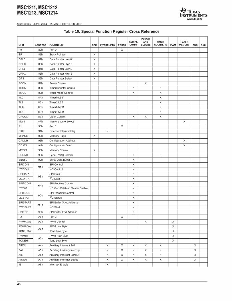
SBAS323G − JUNE 2004 − REVISED OCTOBER 2007
www.ti.com
46
Table 10. Special Function Register Cross Reference
SFR ADDRESS FUNCTIONS CPU INTERRUPTS PORTSSERIALCOMM.
POWERAND
CLOCKSTIMER
COUNTERS PWMFLASH
MEMORY ADC DAC
P0 80h Port 0 X
SP 81h Stack Pointer X
DPL0 82h Data Pointer Low 0 X
DPH0 83h Data Pointer High 0 X
DPL1 84h Data Pointer Low 1 X
DPH1 85h Data Pointer High 1 X
DPS 86h Data Pointer Select X
PCON 87h Power Control X
TCON 88h Timer/Counter Control X X
TMOD 89h Timer Mode Control X X
TL0 8Ah Timer0 LSB X
TL1 8Bh Timer1 LSB X
TH0 8Ch Timer0 MSB X
TH1 8Dh Timer1 MSB X
CKCON 8Eh Clock Control X X X
MWS 8Fh Memory Write Select X
P1 90h Port 1 X
EXIF 91h External Interrupt Flag X
MPAGE 92h Memory Page X
CADDR 93h Configuration Address X
CDATA 94h Configuration Data X
MCON 95h Memory Control X
SCON0 98h Serial Port 0 Control X X
SBUF0 99h Serial Data Buffer 0 X
SPICON9Ah
SPI Control X
I2CCON9Ah
I2C Control X
SPIDATA9Bh
SPI Data X
I2CDATA9Bh
I2C Data X
SPIRCON9Ch
SPI Receive Control X
I2CGM9Ch
I2C Gen Call/Mult Master Enable X
SPITCON9Dh
SPI Transmit Control X
I2CSTAT9Dh
I2C Status X
SPISTART9Eh
SPI Buffer Start Address X
I2CSTART9Eh
I2C Start X
SPIEND 9Fh SPI Buffer End Address X
P2 A0h Port 2 X
PWMCON A1h PWM Control X X
PWMLOWA2h
PWM Low Byte X
TONELOWA2h
Tone Low Byte X
PWMHIA3h
PWM HIgh Byte X
TONEHIA3h
Tone Low Byte X
AIPOL A4h Auxiliary Interrupt Poll X X X X X X
PAI A5h Pending Auxiliary Interrupt X X X X X X
AIE A6h Auxiliary Interrupt Enable X X X X X X
AISTAT A7h Auxiliary Interrupt Status X X X X X X
IE A8h Interrupt Enable X
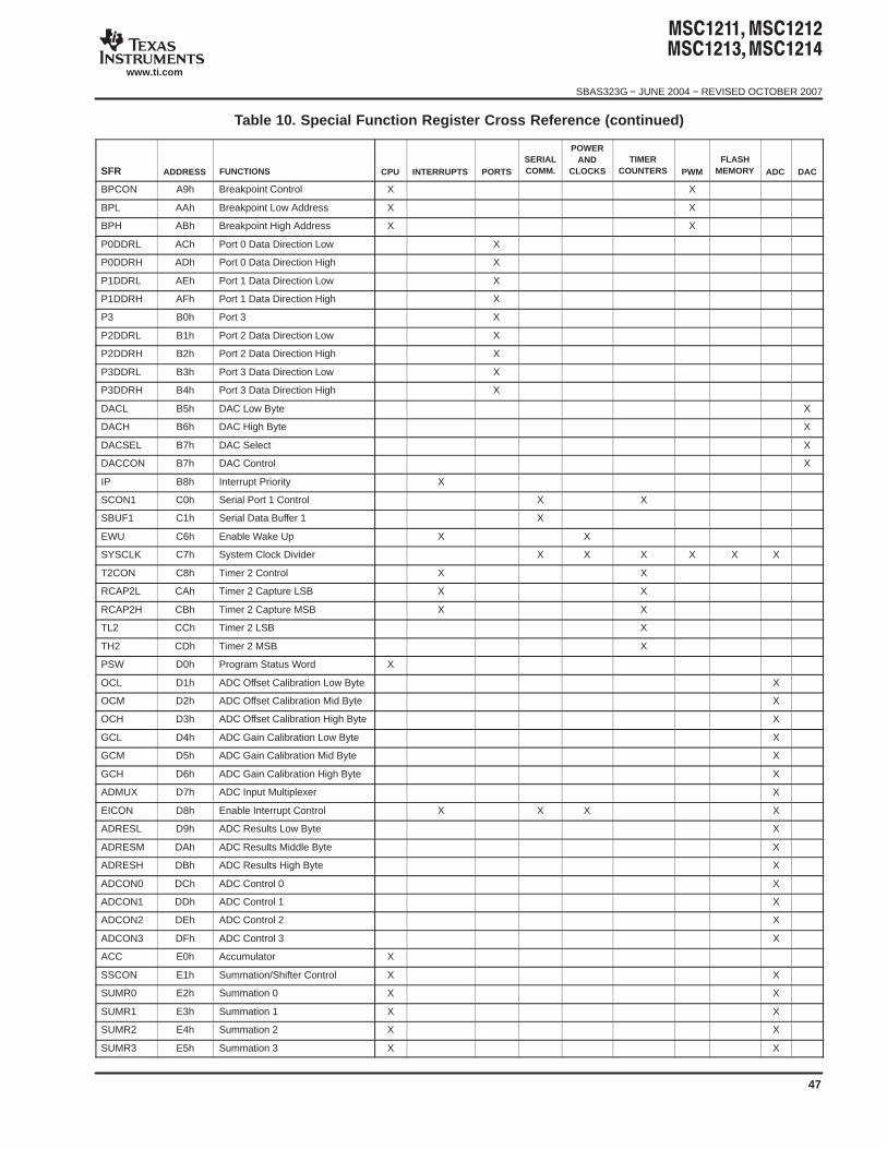
SBAS323G − JUNE 2004 − REVISED OCTOBER 2007
www.ti.com
47
Table 10. Special Function Register Cross Reference (continued)
SFR DACADCFLASH
MEMORYPWMTIMER
COUNTERS
POWERAND
CLOCKSSERIALCOMM.PORTSINTERRUPTSCPUFUNCTIONSADDRESS
BPCON A9h Breakpoint Control X X
BPL AAh Breakpoint Low Address X X
BPH ABh Breakpoint High Address X X
P0DDRL ACh Port 0 Data Direction Low X
P0DDRH ADh Port 0 Data Direction High X
P1DDRL AEh Port 1 Data Direction Low X
P1DDRH AFh Port 1 Data Direction High X
P3 B0h Port 3 X
P2DDRL B1h Port 2 Data Direction Low X
P2DDRH B2h Port 2 Data Direction High X
P3DDRL B3h Port 3 Data Direction Low X
P3DDRH B4h Port 3 Data Direction High X
DACL B5h DAC Low Byte X
DACH B6h DAC High Byte X
DACSEL B7h DAC Select X
DACCON B7h DAC Control X
IP B8h Interrupt Priority X
SCON1 C0h Serial Port 1 Control X X
SBUF1 C1h Serial Data Buffer 1 X
EWU C6h Enable Wake Up X X
SYSCLK C7h System Clock Divider X X X X X X
T2CON C8h Timer 2 Control X X
RCAP2L CAh Timer 2 Capture LSB X X
RCAP2H CBh Timer 2 Capture MSB X X
TL2 CCh Timer 2 LSB X
TH2 CDh Timer 2 MSB X
PSW D0h Program Status Word X
OCL D1h ADC Offset Calibration Low Byte X
OCM D2h ADC Offset Calibration Mid Byte X
OCH D3h ADC Offset Calibration High Byte X
GCL D4h ADC Gain Calibration Low Byte X
GCM D5h ADC Gain Calibration Mid Byte X
GCH D6h ADC Gain Calibration High Byte X
ADMUX D7h ADC Input Multiplexer X
EICON D8h Enable Interrupt Control X X X X
ADRESL D9h ADC Results Low Byte X
ADRESM DAh ADC Results Middle Byte X
ADRESH DBh ADC Results High Byte X
ADCON0 DCh ADC Control 0 X
ADCON1 DDh ADC Control 1 X
ADCON2 DEh ADC Control 2 X
ADCON3 DFh ADC Control 3 X
ACC E0h Accumulator X
SSCON E1h Summation/Shifter Control X X
SUMR0 E2h Summation 0 X X
SUMR1 E3h Summation 1 X X
SUMR2 E4h Summation 2 X X
SUMR3 E5h Summation 3 X X
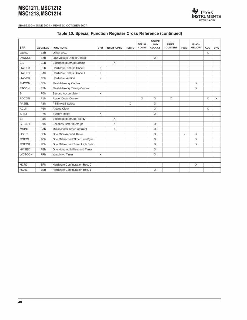
SBAS323G − JUNE 2004 − REVISED OCTOBER 2007
www.ti.com
48
Table 10. Special Function Register Cross Reference (continued)
SFR DACADCFLASH
MEMORYPWMTIMER
COUNTERS
POWERAND
CLOCKSSERIALCOMM.PORTSINTERRUPTSCPUFUNCTIONSADDRESS
ODAC E6h Offset DAC X
LVDCON E7h Low Voltage Detect Control X
EIE E8h Extended Interrupt Enable X
HWPC0 E9h Hardware Product Code 0 X
HWPC1 EAh Hardware Product Code 1 X
HWVER EBh Hardware Version X
FMCON EEh Flash Memory Control X
FTCON EFh Flash Memory Timing Control X
B F0h Second Accumulator X
PDCON F1h Power Down Control X X X X X
PASEL F2h PSEN/ALE Select X X
ACLK F6h Analog Clock X X
SRST F7h System Reset X X
EIP F8h Extended Interrupt Priority X
SECINT F9h Seconds Timer Interrupt X X
MSINT FAh Milliseconds Timer Interrupt X X
USEC FBh One Microsecond TImer X X X
MSECL FCh One Millisecond TImer Low Byte X X
MSECH FDh One Millisecond Timer High Byte X X
HMSEC FEh One Hundred Millisecond TImer X
WDTCON FFh Watchdog Timer X X
HCR0 3Fh Hardware Configuration Reg. 0 X
HCR1 3Eh Hardware Configuration Reg. 1 X
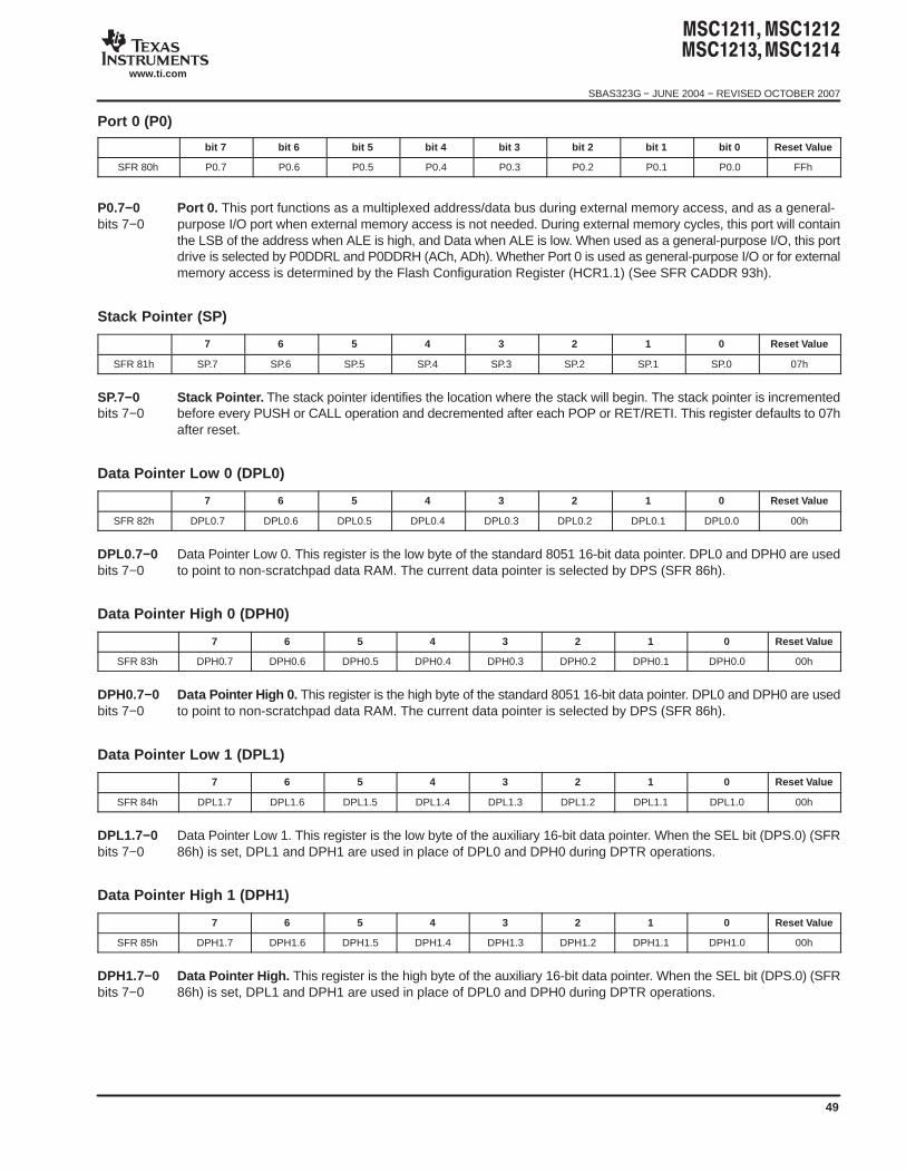
SBAS323G − JUNE 2004 − REVISED OCTOBER 2007
www.ti.com
49
Port 0 (P0)
bit 7 bit 6 bit 5 bit 4 bit 3 bit 2 bit 1 bit 0 Reset Value
SFR 80h P0.7 P0.6 P0.5 P0.4 P0.3 P0.2 P0.1 P0.0 FFh
P0.7−0 Port 0. This port functions as a multiplexed address/data bus during external memory access, and as a general-bits 7−0 purpose I/O port when external memory access is not needed. During external memory cycles, this port will contain
the LSB of the address when ALE is high, and Data when ALE is low. When used as a general-purpose I/O, this portdrive is selected by P0DDRL and P0DDRH (ACh, ADh). Whether Port 0 is used as general-purpose I/O or for externalmemory access is determined by the Flash Configuration Register (HCR1.1) (See SFR CADDR 93h).
Stack Pointer (SP)
7 6 5 4 3 2 1 0 Reset Value
SFR 81h SP.7 SP.6 SP.5 SP.4 SP.3 SP.2 SP.1 SP.0 07h
SP.7−0 Stack Pointer. The stack pointer identifies the location where the stack will begin. The stack pointer is incrementedbits 7−0 before every PUSH or CALL operation and decremented after each POP or RET/RETI. This register defaults to 07h
after reset.
Data Pointer Low 0 (DPL0)
7 6 5 4 3 2 1 0 Reset Value
SFR 82h DPL0.7 DPL0.6 DPL0.5 DPL0.4 DPL0.3 DPL0.2 DPL0.1 DPL0.0 00h
DPL0.7−0 Data Pointer Low 0. This register is the low byte of the standard 8051 16-bit data pointer. DPL0 and DPH0 are usedbits 7−0 to point to non-scratchpad data RAM. The current data pointer is selected by DPS (SFR 86h).
Data Pointer High 0 (DPH0)
7 6 5 4 3 2 1 0 Reset Value
SFR 83h DPH0.7 DPH0.6 DPH0.5 DPH0.4 DPH0.3 DPH0.2 DPH0.1 DPH0.0 00h
DPH0.7−0 Data Pointer High 0. This register is the high byte of the standard 8051 16-bit data pointer. DPL0 and DPH0 are usedbits 7−0 to point to non-scratchpad data RAM. The current data pointer is selected by DPS (SFR 86h).
Data Pointer Low 1 (DPL1)
7 6 5 4 3 2 1 0 Reset Value
SFR 84h DPL1.7 DPL1.6 DPL1.5 DPL1.4 DPL1.3 DPL1.2 DPL1.1 DPL1.0 00h
DPL1.7−0 Data Pointer Low 1. This register is the low byte of the auxiliary 16-bit data pointer. When the SEL bit (DPS.0) (SFRbits 7−0 86h) is set, DPL1 and DPH1 are used in place of DPL0 and DPH0 during DPTR operations.
Data Pointer High 1 (DPH1)
7 6 5 4 3 2 1 0 Reset Value
SFR 85h DPH1.7 DPH1.6 DPH1.5 DPH1.4 DPH1.3 DPH1.2 DPH1.1 DPH1.0 00h
DPH1.7−0 Data Pointer High. This register is the high byte of the auxiliary 16-bit data pointer. When the SEL bit (DPS.0) (SFRbits 7−0 86h) is set, DPL1 and DPH1 are used in place of DPL0 and DPH0 during DPTR operations.
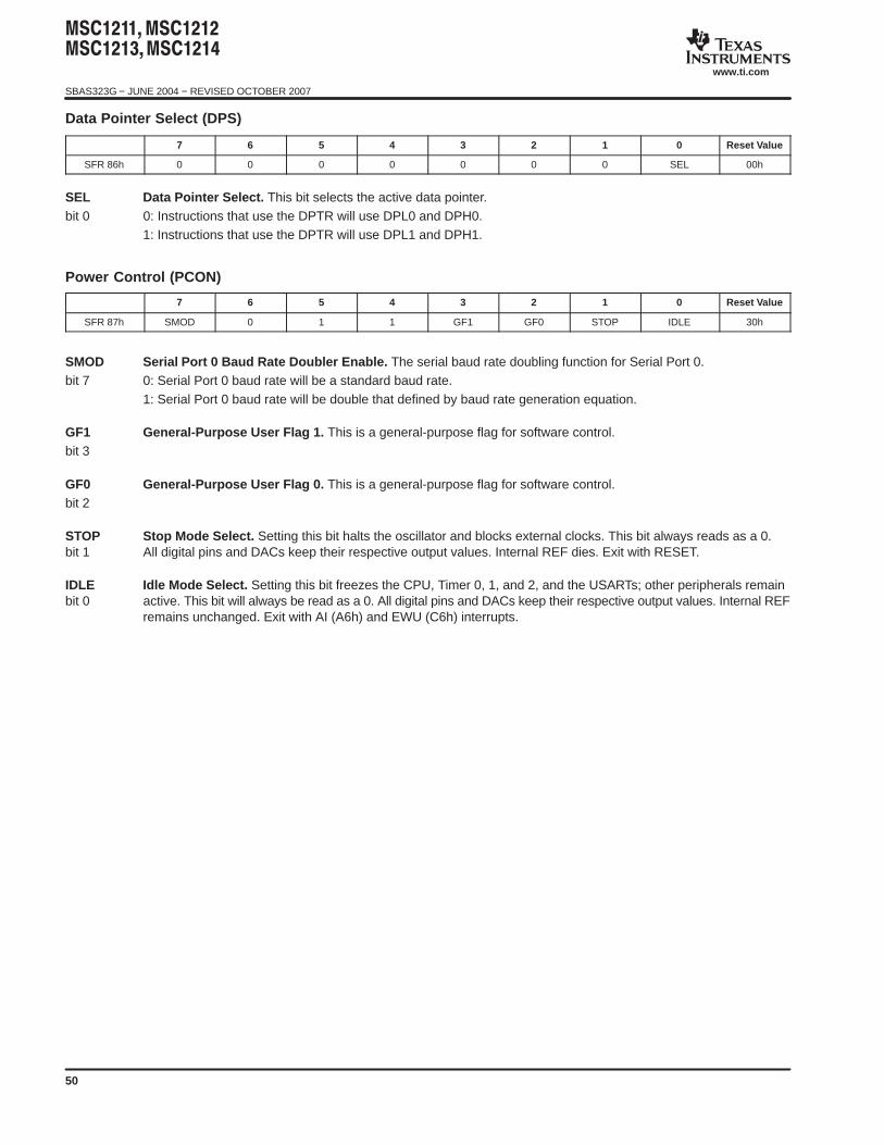
SBAS323G − JUNE 2004 − REVISED OCTOBER 2007
www.ti.com
50
Data Pointer Select (DPS)
7 6 5 4 3 2 1 0 Reset Value
SFR 86h 0 0 0 0 0 0 0 SEL 00h
SEL Data Pointer Select. This bit selects the active data pointer.bit 0 0: Instructions that use the DPTR will use DPL0 and DPH0.
1: Instructions that use the DPTR will use DPL1 and DPH1.
Power Control (PCON)
7 6 5 4 3 2 1 0 Reset Value
SFR 87h SMOD 0 1 1 GF1 GF0 STOP IDLE 30h
SMOD Serial Port 0 Baud Rate Doubler Enable. The serial baud rate doubling function for Serial Port 0.bit 7 0: Serial Port 0 baud rate will be a standard baud rate.
1: Serial Port 0 baud rate will be double that defined by baud rate generation equation.
GF1 General-Purpose User Flag 1. This is a general-purpose flag for software control.bit 3
GF0 General-Purpose User Flag 0. This is a general-purpose flag for software control.bit 2
STOP Stop Mode Select. Setting this bit halts the oscillator and blocks external clocks. This bit always reads as a 0.bit 1 All digital pins and DACs keep their respective output values. Internal REF dies. Exit with RESET.
IDLE Idle Mode Select. Setting this bit freezes the CPU, Timer 0, 1, and 2, and the USARTs; other peripherals remainbit 0 active. This bit will always be read as a 0. All digital pins and DACs keep their respective output values. Internal REF
remains unchanged. Exit with AI (A6h) and EWU (C6h) interrupts.
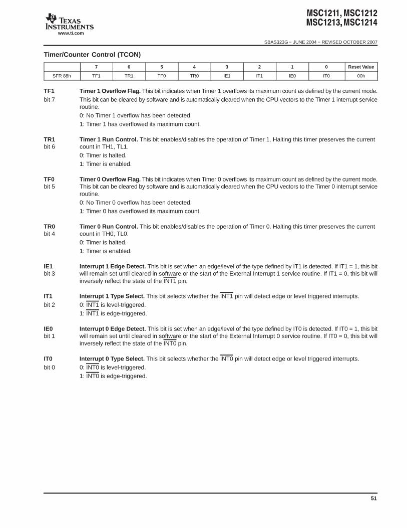
SBAS323G − JUNE 2004 − REVISED OCTOBER 2007
www.ti.com
51
Timer/Counter Control (TCON)
7 6 5 4 3 2 1 0 Reset Value
SFR 88h TF1 TR1 TF0 TR0 IE1 IT1 IE0 IT0 00h
TF1 Timer 1 Overflow Flag. This bit indicates when Timer 1 overflows its maximum count as defined by the current mode.bit 7 This bit can be cleared by software and is automatically cleared when the CPU vectors to the Timer 1 interrupt service
routine.0: No Timer 1 overflow has been detected.1: Timer 1 has overflowed its maximum count.
TR1 Timer 1 Run Control. This bit enables/disables the operation of Timer 1. Halting this timer preserves the currentbit 6 count in TH1, TL1.
0: Timer is halted.1: Timer is enabled.
TF0 Timer 0 Overflow Flag. This bit indicates when Timer 0 overflows its maximum count as defined by the current mode.bit 5 This bit can be cleared by software and is automatically cleared when the CPU vectors to the Timer 0 interrupt service
routine.0: No Timer 0 overflow has been detected.1: Timer 0 has overflowed its maximum count.
TR0 Timer 0 Run Control. This bit enables/disables the operation of Timer 0. Halting this timer preserves the currentbit 4 count in TH0, TL0.
0: Timer is halted.1: Timer is enabled.
IE1 Interrupt 1 Edge Detect. This bit is set when an edge/level of the type defined by IT1 is detected. If IT1 = 1, this bitbit 3 will remain set until cleared in software or the start of the External Interrupt 1 service routine. If IT1 = 0, this bit will
inversely reflect the state of the INT1 pin.
IT1 Interrupt 1 Type Select. This bit selects whether the INT1 pin will detect edge or level triggered interrupts.bit 2 0: INT1 is level-triggered.
1: INT1 is edge-triggered.
IE0 Interrupt 0 Edge Detect. This bit is set when an edge/level of the type defined by IT0 is detected. If IT0 = 1, this bitbit 1 will remain set until cleared in software or the start of the External Interrupt 0 service routine. If IT0 = 0, this bit will
inversely reflect the state of the INT0 pin.
IT0 Interrupt 0 Type Select. This bit selects whether the INT0 pin will detect edge or level triggered interrupts.bit 0 0: INT0 is level-triggered.
1: INT0 is edge-triggered.
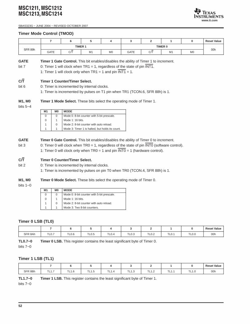
SBAS323G − JUNE 2004 − REVISED OCTOBER 2007
www.ti.com
52
Timer Mode Control (TMOD)
7 6 5 4 3 2 1 0 Reset Value
SFR 89hTIMER 1 TIMER 0
00hSFR 89hGATE C/T M1 M0 GATE C/T M1 M0
00h
GATE Timer 1 Gate Control. This bit enables/disables the ability of Timer 1 to increment.bit 7 0: Timer 1 will clock when TR1 = 1, regardless of the state of pin INT1.
1: Timer 1 will clock only when TR1 = 1 and pin INT1 = 1.
C/T Timer 1 Counter/Timer Select.bit 6 0: Timer is incremented by internal clocks.
1: Timer is incremented by pulses on T1 pin when TR1 (TCON.6, SFR 88h) is 1.
M1, M0 Timer 1 Mode Select. These bits select the operating mode of Timer 1.bits 5−4
M1 M0 MODE
0 0 Mode 0: 8-bit counter with 5-bit prescale.
0 1 Mode 1: 16 bits.
1 0 Mode 2: 8-bit counter with auto reload.
1 1 Mode 3: Timer 1 is halted, but holds its count.
GATE Timer 0 Gate Control. This bit enables/disables the ability of Timer 0 to increment.bit 3 0: Timer 0 will clock when TR0 = 1, regardless of the state of pin INT0 (software control).
1: Timer 0 will clock only when TR0 = 1 and pin INT0 = 1 (hardware control).
C/T Timer 0 Counter/Timer Select.bit 2 0: Timer is incremented by internal clocks.
1: Timer is incremented by pulses on pin T0 when TR0 (TCON.4, SFR 88h) is 1.
M1, M0 Timer 0 Mode Select. These bits select the operating mode of Timer 0.bits 1−0
M1 M0 MODE
0 0 Mode 0: 8-bit counter with 5-bit prescale.
0 1 Mode 1: 16 bits.
1 0 Mode 2: 8-bit counter with auto reload.
1 1 Mode 3: Two 8-bit counters.
Timer 0 LSB (TL0)
7 6 5 4 3 2 1 0 Reset Value
SFR 8Ah TL0.7 TL0.6 TL0.5 TL0.4 TL0.3 TL0.2 TL0.1 TL0.0 00h
TL0.7−0 Timer 0 LSB. This register contains the least significant byte of Timer 0.bits 7−0
Timer 1 LSB (TL1)
7 6 5 4 3 2 1 0 Reset Value
SFR 8Bh TL1.7 TL1.6 TL1.5 TL1.4 TL1.3 TL1.2 TL1.1 TL1.0 00h
TL1.7−0 Timer 1 LSB. This register contains the least significant byte of Timer 1.bits 7−0
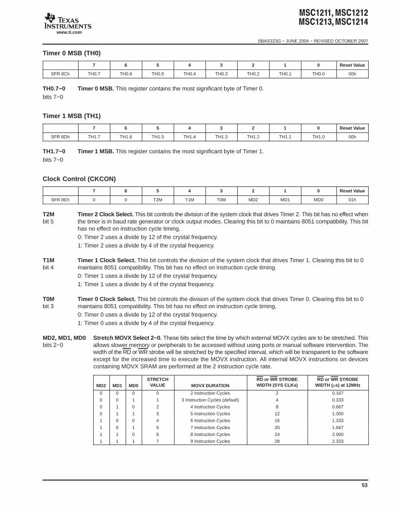
SBAS323G − JUNE 2004 − REVISED OCTOBER 2007
www.ti.com
53
Timer 0 MSB (TH0)
7 6 5 4 3 2 1 0 Reset Value
SFR 8Ch TH0.7 TH0.6 TH0.5 TH0.4 TH0.3 TH0.2 TH0.1 TH0.0 00h
TH0.7−0 Timer 0 MSB. This register contains the most significant byte of Timer 0.bits 7−0
Timer 1 MSB (TH1)
7 6 5 4 3 2 1 0 Reset Value
SFR 8Dh TH1.7 TH1.6 TH1.5 TH1.4 TH1.3 TH1.2 TH1.1 TH1.0 00h
TH1.7−0 Timer 1 MSB. This register contains the most significant byte of Timer 1.bits 7−0
Clock Control (CKCON)
7 6 5 4 3 2 1 0 Reset Value
SFR 8Eh 0 0 T2M T1M T0M MD2 MD1 MD0 01h
T2M Timer 2 Clock Select. This bit controls the division of the system clock that drives Timer 2. This bit has no effect whenbit 5 the timer is in baud rate generator or clock output modes. Clearing this bit to 0 maintains 8051 compatibility. This bit
has no effect on instruction cycle timing.0: Timer 2 uses a divide by 12 of the crystal frequency.1: Timer 2 uses a divide by 4 of the crystal frequency.
T1M Timer 1 Clock Select. This bit controls the division of the system clock that drives Timer 1. Clearing this bit to 0bit 4 maintains 8051 compatibility. This bit has no effect on instruction cycle timing.
0: Timer 1 uses a divide by 12 of the crystal frequency.1: Timer 1 uses a divide by 4 of the crystal frequency.
T0M Timer 0 Clock Select. This bit controls the division of the system clock that drives Timer 0. Clearing this bit to 0bit 3 maintains 8051 compatibility. This bit has no effect on instruction cycle timing.
0: Timer 0 uses a divide by 12 of the crystal frequency.1: Timer 0 uses a divide by 4 of the crystal frequency.
MD2, MD1, MD0 Stretch MOVX Select 2−0. These bits select the time by which external MOVX cycles are to be stretched. Thisbits 2−0 allows slower memory or peripherals to be accessed without using ports or manual software intervention. The
width of the RD or WR strobe will be stretched by the specified interval, which will be transparent to the softwareexcept for the increased time to execute the MOVX instruction. All internal MOVX instructions on devicescontaining MOVX SRAM are performed at the 2 instruction cycle rate.
MD2 MD1 MD0STRETCH
VALUE MOVX DURATIONRD or WR STROBEWIDTH (SYS CLKs)
RD or WR STROBEWIDTH (s) at 12MHz
0 0 0 0 2 Instruction Cycles 2 0.167
0 0 1 1 3 Instruction Cycles (default) 4 0.333
0 1 0 2 4 Instruction Cycles 8 0.667
0 1 1 3 5 Instruction Cycles 12 1.000
1 0 0 4 6 Instruction Cycles 16 1.333
1 0 1 5 7 Instruction Cycles 20 1.667
1 1 0 6 8 Instruction Cycles 24 2.000
1 1 1 7 9 Instruction Cycles 28 2.333
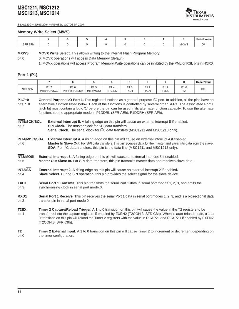
SBAS323G − JUNE 2004 − REVISED OCTOBER 2007
www.ti.com
54
Memory Write Select (MWS)
7 6 5 4 3 2 1 0 Reset Value
SFR 8Fh 0 0 0 0 0 0 0 MXWS 00h
MXWS MOVX Write Select. This allows writing to the internal Flash Program Memory.bit 0 0: MOVX operations will access Data Memory (default).
1: MOVX operations will access Program Memory. Write operations can be inhibited by the PML or RSL bits in HCR0.
Port 1 (P1)
7 6 5 4 3 2 1 0 Reset Value
SFR 90hP1.7
INT5/SCK/SCLP1.6
INT4/MISO/SDAP1.5
INT3/MOSIP1.4
INT2/SSP1.3TXD1
P1.2RXD1
P1.1T2EX
P1.0T2
FFh
P1.7−0 General-Purpose I/O Port 1. This register functions as a general-purpose I/O port. In addition, all the pins have anbits 7−0 alternative function listed below. Each of the functions is controlled by several other SFRs. The associated Port 1
latch bit must contain a logic ‘1’ before the pin can be used in its alternate function capacity. To use the alternatefunction, set the appropriate mode in P1DDRL (SFR AEh), P1DDRH (SFR AFh).
INT5/SCK/SCL External Interrupt 5. A falling edge on this pin will cause an external interrupt 5 if enabled.bit 7 SPI Clock. The master clock for SPI data transfers.
Serial Clock. The serial clock for I2C data transfers (MSC1211 and MSC1213 only).
INT4/MISO/SDA External Interrupt 4. A rising edge on this pin will cause an external interrupt 4 if enabled.bit 6 Master In Slave Out. For SPI data transfers, this pin receives data for the master and transmits data from the slave.
SDA. For I2C data transfers, this pin is the data line (MSC1211 and MSC1213 only).
NT3/MOSI External Interrupt 3. A falling edge on this pin will cause an external interrupt 3 if enabled.bit 5 Master Out Slave In. For SPI data transfers, this pin transmits master data and receives slave data.
INT2/SS External Interrupt 2. A rising edge on this pin will cause an external interrupt 2 if enabled.bit 4 Slave Select. During SPI operation, this pin provides the select signal for the slave device.
TXD1 Serial Port 1 Transmit. This pin transmits the serial Port 1 data in serial port modes 1, 2, 3, and emits thebit 3 synchronizing clock in serial port mode 0.
RXD1 Serial Port 1 Receive. This pin receives the serial Port 1 data in serial port modes 1, 2, 3, and is a bidirectional databit 2 transfer pin in serial port mode 0.
T2EX Timer 2 Capture/Reload Trigger. A 1 to 0 transition on this pin will cause the value in the T2 registers to bebit 1 transferred into the capture registers if enabled by EXEN2 (T2CON.3, SFR C8h). When in auto-reload mode, a 1 to
0 transition on this pin will reload the Timer 2 registers with the value in RCAP2L and RCAP2H if enabled by EXEN2(T2CON.3, SFR C8h).
T2 Timer 2 External Input. A 1 to 0 transition on this pin will cause Timer 2 to increment or decrement depending onbit 0 the timer configuration.
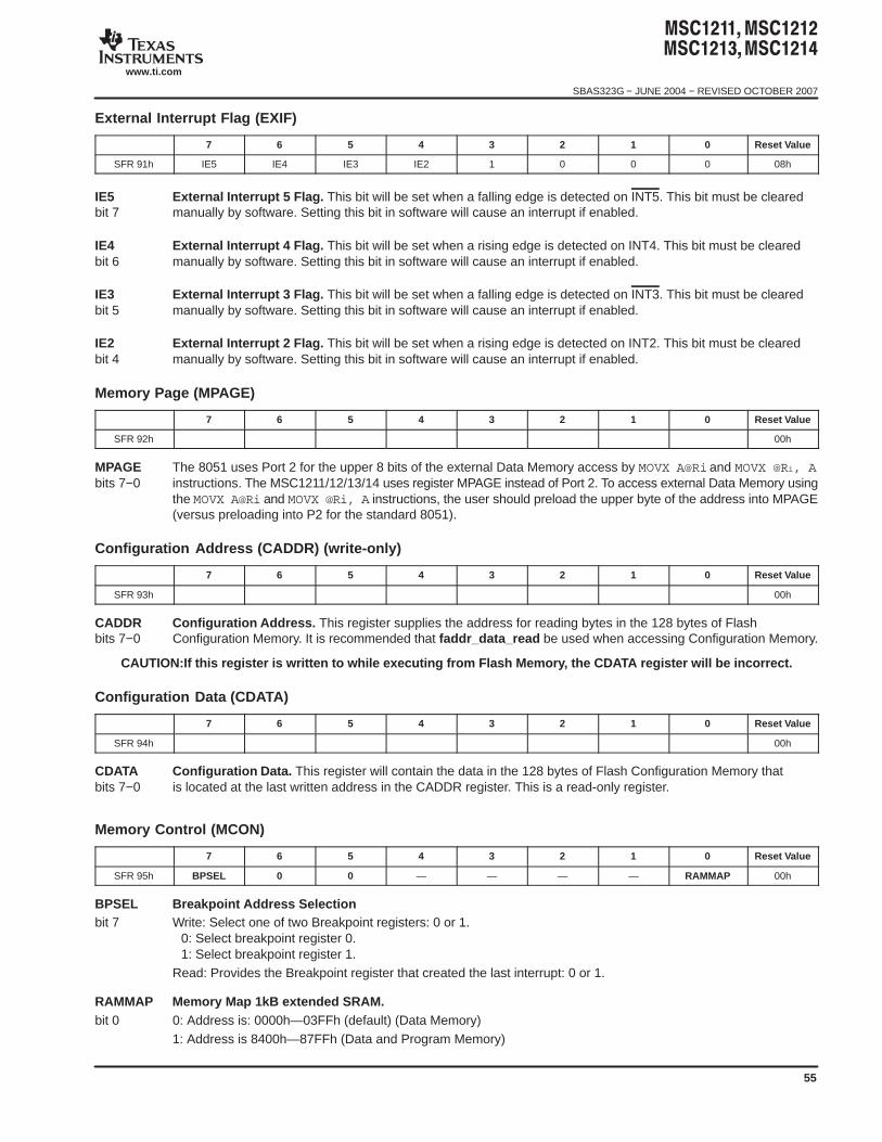
SBAS323G − JUNE 2004 − REVISED OCTOBER 2007
www.ti.com
55
External Interrupt Flag (EXIF)
7 6 5 4 3 2 1 0 Reset Value
SFR 91h IE5 IE4 IE3 IE2 1 0 0 0 08h
IE5 External Interrupt 5 Flag. This bit will be set when a falling edge is detected on INT5. This bit must be clearedbit 7 manually by software. Setting this bit in software will cause an interrupt if enabled.
IE4 External Interrupt 4 Flag. This bit will be set when a rising edge is detected on INT4. This bit must be clearedbit 6 manually by software. Setting this bit in software will cause an interrupt if enabled.
IE3 External Interrupt 3 Flag. This bit will be set when a falling edge is detected on INT3. This bit must be clearedbit 5 manually by software. Setting this bit in software will cause an interrupt if enabled.
IE2 External Interrupt 2 Flag. This bit will be set when a rising edge is detected on INT2. This bit must be clearedbit 4 manually by software. Setting this bit in software will cause an interrupt if enabled.
Memory Page (MPAGE)
7 6 5 4 3 2 1 0 Reset Value
SFR 92h 00h
MPAGE The 8051 uses Port 2 for the upper 8 bits of the external Data Memory access by MOVX A@Ri and MOVX @Ri, Abits 7−0 instructions. The MSC1211/12/13/14 uses register MPAGE instead of Port 2. To access external Data Memory using
the MOVX A@Ri and MOVX @Ri, A instructions, the user should preload the upper byte of the address into MPAGE(versus preloading into P2 for the standard 8051).
Configuration Address (CADDR) (write-only)
7 6 5 4 3 2 1 0 Reset Value
SFR 93h 00h
CADDR Configuration Address. This register supplies the address for reading bytes in the 128 bytes of Flashbits 7−0 Configuration Memory. It is recommended that faddr_data_read be used when accessing Configuration Memory.
CAUTION:If this register is written to while executing from Flash Memory, the CDATA register will be incorrect.
Configuration Data (CDATA)
7 6 5 4 3 2 1 0 Reset Value
SFR 94h 00h
CDATA Configuration Data. This register will contain the data in the 128 bytes of Flash Configuration Memory thatbits 7−0 is located at the last written address in the CADDR register. This is a read-only register.
Memory Control (MCON)
7 6 5 4 3 2 1 0 Reset Value
SFR 95h BPSEL 0 0 — — — — RAMMAP 00h
BPSEL Breakpoint Address Selectionbit 7 Write: Select one of two Breakpoint registers: 0 or 1.
0: Select breakpoint register 0.1: Select breakpoint register 1.
Read: Provides the Breakpoint register that created the last interrupt: 0 or 1.
RAMMAP Memory Map 1kB extended SRAM.bit 0 0: Address is: 0000h—03FFh (default) (Data Memory)
1: Address is 8400h—87FFh (Data and Program Memory)
SBAS323G − JUNE 2004 − REVISED OCTOBER 2007
www.ti.com
56
Serial Port 0 Control (SCON0)
7 6 5 4 3 2 1 0 Reset Value
SFR 98h SM0_0 SM1_0 SM2_0 REN_0 TB8_0 RB8_0 TI_0 RI_0 00h
SM0−2 Serial Port 0 Mode. These bits control the mode of serial Port 0. Modes 1, 2, and 3 have 1 start and 1 stop bit inbits 7−5 addition to the 8 or 9 data bits.
MODE SM0 SM1 SM2 FUNCTION LENGTH PERIOD
0 0 0 0 Synchronous 8 bits 12 pCLK(1)
0 0 0 1 Synchronous 8 bits 4 pCLK(1)
1(2) 0 1 0 Asynchronous 10 bits Timer 1 or 2 Baud Rate Equation
1(2) 0 1 1 Valid Stop Required(3) 10 bits Timer 1 Baud Rate Equation
2 1 0 0 Asynchronous 11 bits 64 pCLK(1) (SMOD = 0)32 pCLK(1) (SMOD = 1)
2 1 0 1 Asynchronous with Multiprocessor Communication(4) 11 bits 64 pCLK(1) (SMOD = 0)32 pCLK(1) (SMOD = 1)
3(2) 1 1 0 Asynchronous 11 bits Timer 1 or 2 Baud Rate Equation
3(2) 1 1 1 Asynchronous with Multiprocessor Communication(4) 11 bits Timer 1 or 2 Baud Rate Equation
(1) pCLK will be equal to tCLK, except that pCLK will stop for Idle mode.(2) For modes 1 and 3, the selection of Timer 1 or 2 for baud rate is specified via the T2CON (C8h) register.(3) RI_0 will only be activated when a valid STOP is received.(4) RI_0 will not be activated if bit 9 = 0.
REN_0 Receive Enable. This bit enables/disables the serial Port 0 received shift register.bit 4 0: Serial Port 0 reception disabled.
1: Serial Port 0 received enabled (modes 1, 2, and 3). Initiate synchronous reception (mode 0).
TB8_0 9th Transmission Bit State. This bit defines the state of the 9th transmission bit in serial Port 0 modes 2 and 3.bit 3
RB8_0 9th Received Bit State. This bit identifies the state of the 9th reception bit of received data in serial Port 0 modesbit 2 2 and 3. In serial port mode 1, when SM2_0 = 0, RB8_0 is the state of the stop bit. RB8_0 is not used in mode 0.
TI_0 Transmitter Interrupt Flag. This bit indicates that data in the serial Port 0 buffer has been completely shifted out. In serialbit 1 port mode 0, TI_0 is set at the end of the 8th data bit. In all other modes, this bit is set at the end of the last data bit.
This bit must be manually cleared by software.
RI_0 Receiver Interrupt Flag. This bit indicates that a byte of data has been received in the serial Port 0 buffer. In serialbit 0 port mode 0, RI_0 is set at the end of the 8th bit. In serial port mode 1, RI_0 is set after the last sample of the incoming
stop bit subject to the state of SM2_0. In modes 2 and 3, RI_0 is set after the last sample of RB8_0. This bit mustbe manually cleared by software.
Serial Data Buffer 0 (SBUF0)
7 6 5 4 3 2 1 0 Reset Value
SFR 99h 00h
SBUF0 Serial Data Buffer 0. Data for Serial Port 0 is read from or written to this location. The serial transmit and receivebits 7−0 buffers are separate registers, but both are addressed at this location.
SBAS323G − JUNE 2004 − REVISED OCTOBER 2007
www.ti.com
57
SPI Control (SPICON). Any change resets the SPI interface, counters, and pointers.
7 6 5 4 3 2 1 0 Reset Value
SFR 9Ah SCK2 SCK1 SCK0 FIFO ORDER MSTR CPHA CPOL 00h
SCK SCK Selection. Selection of tCLK divider for generation of SCK in Master mode.bits 7−5
SCK2 SCK1 SCK0 SCK PERIOD
0 0 0 tCLK/2
0 0 1 tCLK/4
0 1 0 tCLK/8
0 1 1 tCLK/16
1 0 0 tCLK/32
1 0 1 tCLK/64
1 1 0 tCLK/128
1 1 1 tCLK/256
FIFO Enable FIFO in On-Chip Indirect Memory.bit 4 0: Both transmit and receive are double buffers
1: Circular FIFO used for transmit and receive bytes
ORDER Set Bit Order for Transmit and Receive.bit 3 0: Most Significant Bits First
1: Least Significant Bits First
MSTR SPI Master Mode.bit 2 0: Slave Mode
1: Master Mode
CPHA Serial Clock Phase Control.bit 1 0: Valid data starting from half SCK period before the first edge of SCK
1: Valid data starting from the first edge of SCK
CPOL Serial Clock Polarity.bit 0 0: SCK idle at logic low
1: SCK idle at logic high
SBAS323G − JUNE 2004 − REVISED OCTOBER 2007
www.ti.com
58
I2C Control (I2CCON) (Available only on the MSC1211 and MSC1213)
7 6 5 4 3 2 1 0 Reset Value
SFR 9Ah START STOP ACK 0 FAST MSTR SCLS FILEN 00h
START Start Condition (Master mode).bit 7 Read: Current status of start condition or repeated start condition.
Write: When operating as a master, a start condition is transmitted when the START bit is set to 1. During a datatransfer, if the START bit is set, a repeated start is transmitted after the current data transfer is complete. If no transferis in progress when the START and STOP bits are set simultaneously, a START will be followed by a STOP.
STOP Stop Condition (Master mode).bit 6 Read: Current status of stop condition.
Write: Setting STOP to logic 1 causes a stop condition to be transmitted. When a stop condition is received, hardwareclears STOP to logic 0. If both START and STOP are set during a transfer, a stop condition is transmitted followedby a start condition.
ACK Acknowledge. Defines the ACK/NACK generation from the master/slave receiver during the acknowledge cycle.bit 5 0: A NACK (high level on SDA) is returned during the acknowledge cycle.
1: An ACK (low level on SDA) is returned during the acknowledge cycle.In slave transmit mode, 0 = Current byte is last byte, 1 = More to follow.
0 Always set this value to zero.bit 4
FAST Fast Mode Enable.bit 3 0: Standard Mode (100kHz)
1: Fast Mode (400kHz)
MSTR SPI Master Mode.bit 2 0: Slave Mode
1: Master Mode
SCLS Clock Stretch.bit 1 0: No effect
1: Release the clock line. For the slave mode, the clock is stretched for each data transfer. This bit releases the clock.
FILEN Filter Enable. 50ns glitch filter.bit 0 0: Filter disabled
1: Filter enabled
SPI Data (SPIDATA) / I 2C Data (I2CDATA)
7 6 5 4 3 2 1 0 Reset Value
SFR 9Bh 00h
SPIDATA SPI Data. Data for SPI is read from or written to this location. The SPI transmit and receive buffers arebits 7−0 separate registers, but both are addressed at this location. Read to clear the receive interrupt and write to clear the
transmit interrupt.
I2CDATA I2C Data . (MSC1211 and MSC1213 only.) Data for I2C is read from or written to this location. The I2C transmit andreceive buffers are separate registers, but both are addressed at this location. Writing to this register
bits 7−0 starts transmission. In Master mode, reading this register starts a Master read cycle.
SBAS323G − JUNE 2004 − REVISED OCTOBER 2007
www.ti.com
59
SPI Receive Control (SPIRCON)
7 6 5 4 3 2 1 0 Reset Value
SFR 9ChRXCNT7
RXFLUSHRXCNT6 RXCNT5 RXCNT4 RXCNT3
RXCNT2RXIRQ2
RXCNT1RXIRQ1
RXCNT0RXIRQ0
00h
RXCNT Receive Counter. Read-only bits which read the number of bytes in the receive buffer (0 to 128).bits 7−0
RXFLUSH Flush Receive FIFO. Write-only.bit 7 0: No Action
1: SPI Receive Buffer Set to Empty
RXIRQ Read IRQ Level. Write-only.bits 2−0
000 Generate IRQ when Receive Count = 1 or more.001 Generate IRQ when Receive Count = 2 or more.
010 Generate IRQ when Receive Count = 4 or more.011 Generate IRQ when Receive Count = 8 or more.100 Generate IRQ when Receive Count = 16 or more.101 Generate IRQ when Receive Count = 32 or more.110 Generate IRQ when Receive Count = 64 or more.111 Generate IRQ when Receive Count = 128 or more.
I2C GM (I2CGM) (Available only on the MSC1211 and MSC1213)
7 6 5 4 3 2 1 0 Reset Value
SFR 9Ch GCMEN 00h
GCMEN General Call/Multiple Master Enable. Write-only.bit 7 Slave mode: 0 = General call ignored, 1 = General call will be detected
Master mode: 0 = Single master, 1 = Multiple master mode
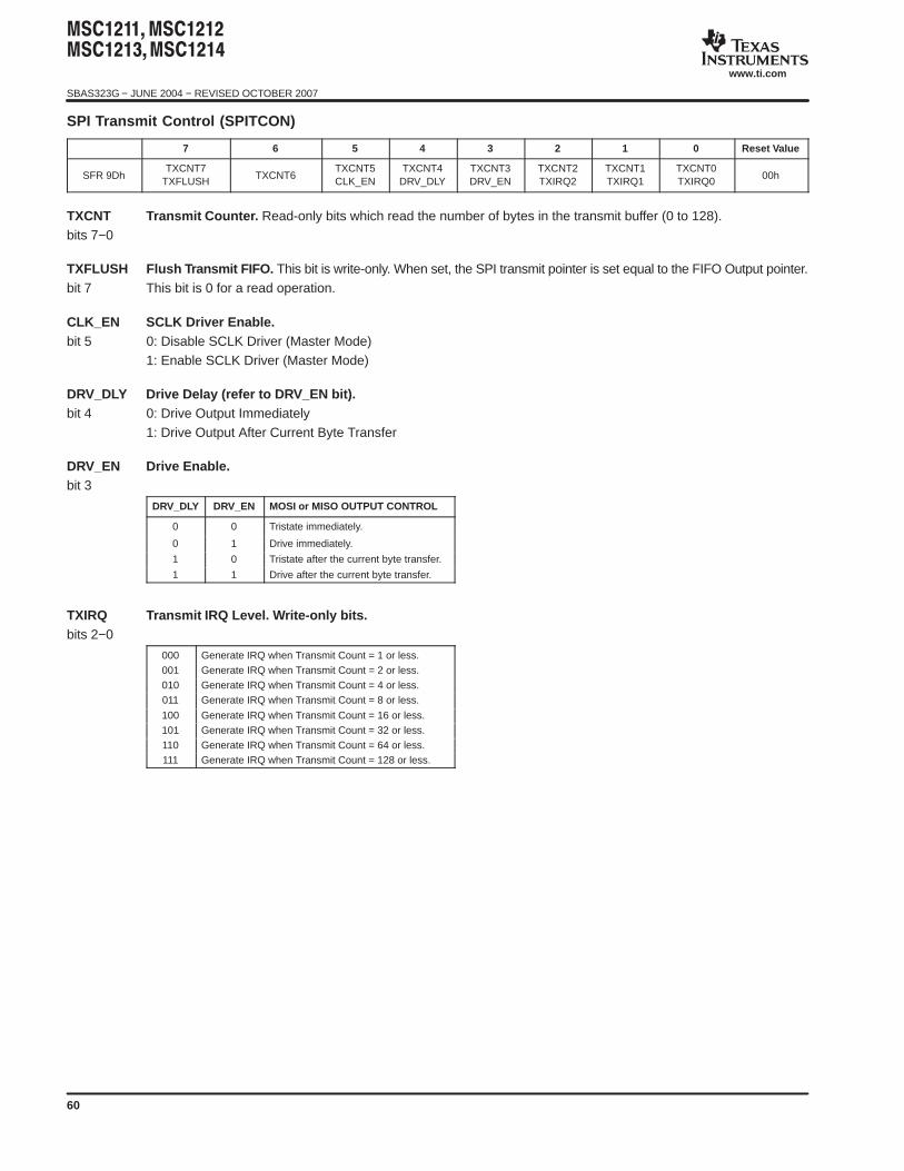
SBAS323G − JUNE 2004 − REVISED OCTOBER 2007
www.ti.com
60
SPI Transmit Control (SPITCON)
7 6 5 4 3 2 1 0 Reset Value
SFR 9DhTXCNT7
TXFLUSHTXCNT6
TXCNT5CLK_EN
TXCNT4DRV_DLY
TXCNT3DRV_EN
TXCNT2TXIRQ2
TXCNT1TXIRQ1
TXCNT0TXIRQ0
00h
TXCNT Transmit Counter. Read-only bits which read the number of bytes in the transmit buffer (0 to 128).bits 7−0
TXFLUSH Flush T ransmit FIFO. This bit is write-only. When set, the SPI transmit pointer is set equal to the FIFO Output pointer.bit 7 This bit is 0 for a read operation.
CLK_EN SCLK Driver Enable.bit 5 0: Disable SCLK Driver (Master Mode)
1: Enable SCLK Driver (Master Mode)
DRV_DLY Drive Delay (refer to DRV_EN bit).bit 4 0: Drive Output Immediately
1: Drive Output After Current Byte Transfer
DRV_EN Drive Enable.bit 3
DRV_DLY DRV_EN MOSI or MISO OUTPUT CONTROL
0 0 Tristate immediately.
0 1 Drive immediately.
1 0 Tristate after the current byte transfer.
1 1 Drive after the current byte transfer.
TXIRQ Transmit IRQ Level. Write-only bits.bits 2−0
000 Generate IRQ when Transmit Count = 1 or less.001 Generate IRQ when Transmit Count = 2 or less.010 Generate IRQ when Transmit Count = 4 or less.011 Generate IRQ when Transmit Count = 8 or less.
100 Generate IRQ when Transmit Count = 16 or less.101 Generate IRQ when Transmit Count = 32 or less.110 Generate IRQ when Transmit Count = 64 or less.111 Generate IRQ when Transmit Count = 128 or less.
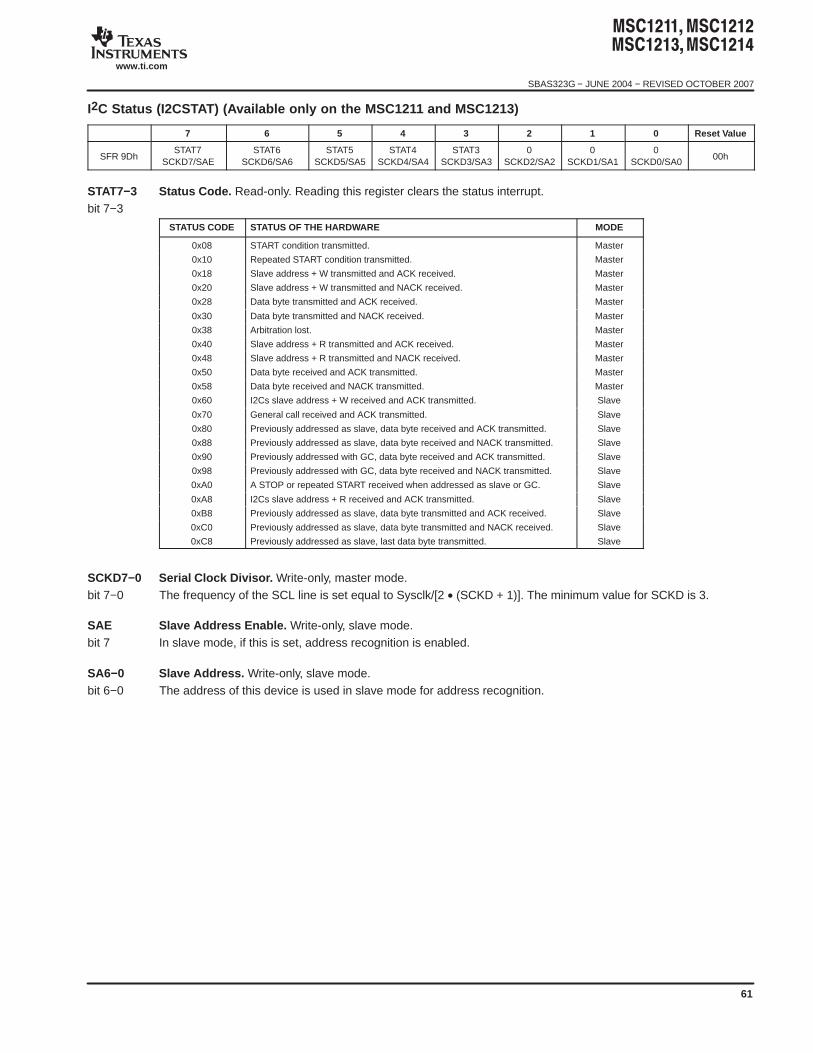
SBAS323G − JUNE 2004 − REVISED OCTOBER 2007
www.ti.com
61
I2C Status (I2CSTAT) (Available only on the MSC1211 and MSC1213)
7 6 5 4 3 2 1 0 Reset Value
SFR 9DhSTAT7
SCKD7/SAESTAT6
SCKD6/SA6STAT5
SCKD5/SA5STAT4
SCKD4/SA4STAT3
SCKD3/SA30
SCKD2/SA20
SCKD1/SA10
SCKD0/SA000h
STAT7−3 Status Code. Read-only. Reading this register clears the status interrupt.bit 7−3
STATUS CODE STATUS OF THE HARDWARE MODE
0x08 START condition transmitted. Master
0x10 Repeated START condition transmitted. Master
0x18 Slave address + W transmitted and ACK received. Master
0x20 Slave address + W transmitted and NACK received. Master
0x28 Data byte transmitted and ACK received. Master
0x30 Data byte transmitted and NACK received. Master
0x38 Arbitration lost. Master
0x40 Slave address + R transmitted and ACK received. Master
0x48 Slave address + R transmitted and NACK received. Master
0x50 Data byte received and ACK transmitted. Master
0x58 Data byte received and NACK transmitted. Master
0x60 I2Cs slave address + W received and ACK transmitted. Slave
0x70 General call received and ACK transmitted. Slave
0x80 Previously addressed as slave, data byte received and ACK transmitted. Slave
0x88 Previously addressed as slave, data byte received and NACK transmitted. Slave
0x90 Previously addressed with GC, data byte received and ACK transmitted. Slave
0x98 Previously addressed with GC, data byte received and NACK transmitted. Slave
0xA0 A STOP or repeated START received when addressed as slave or GC. Slave
0xA8 I2Cs slave address + R received and ACK transmitted. Slave
0xB8 Previously addressed as slave, data byte transmitted and ACK received. Slave
0xC0 Previously addressed as slave, data byte transmitted and NACK received. Slave
0xC8 Previously addressed as slave, last data byte transmitted. Slave
SCKD7−0 Serial Clock Divisor. Write-only, master mode.bit 7−0 The frequency of the SCL line is set equal to Sysclk/[2 • (SCKD + 1)]. The minimum value for SCKD is 3.
SAE Slave Address Enable. Write-only, slave mode.bit 7 In slave mode, if this is set, address recognition is enabled.
SA6−0 Slave Address. Write-only, slave mode.bit 6−0 The address of this device is used in slave mode for address recognition.
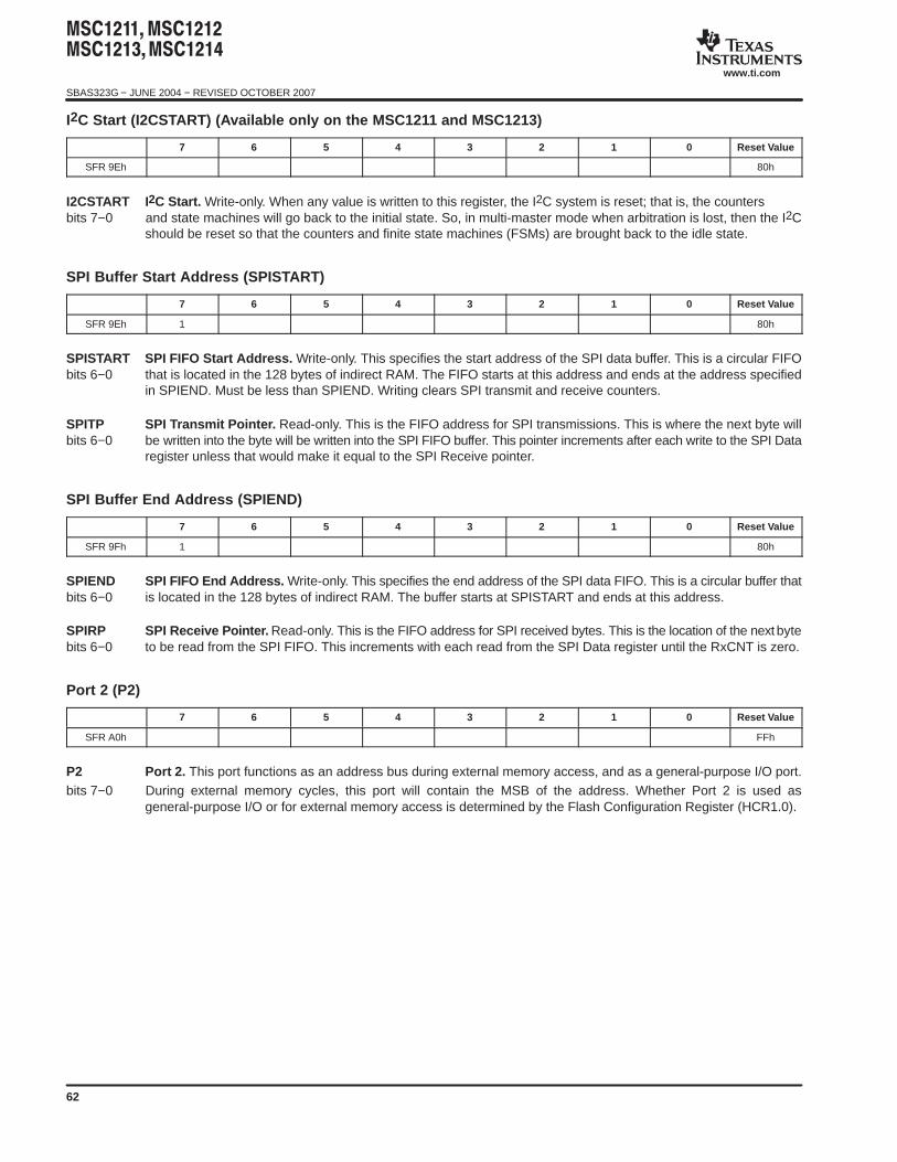
SBAS323G − JUNE 2004 − REVISED OCTOBER 2007
www.ti.com
62
I2C Start (I2CSTART) (Available only on the MSC1211 and MSC1213)
7 6 5 4 3 2 1 0 Reset Value
SFR 9Eh 80h
I2CSTART I2C Start. Write-only. When any value is written to this register, the I2C system is reset; that is, the countersbits 7−0 and state machines will go back to the initial state. So, in multi-master mode when arbitration is lost, then the I2C
should be reset so that the counters and finite state machines (FSMs) are brought back to the idle state.
SPI Buffer Start Address (SPISTART)
7 6 5 4 3 2 1 0 Reset Value
SFR 9Eh 1 80h
SPISTART SPI FIFO Start Address. Write-only. This specifies the start address of the SPI data buffer. This is a circular FIFObits 6−0 that is located in the 128 bytes of indirect RAM. The FIFO starts at this address and ends at the address specified
in SPIEND. Must be less than SPIEND. Writing clears SPI transmit and receive counters.
SPITP SPI Transmit Pointer. Read-only. This is the FIFO address for SPI transmissions. This is where the next byte willbits 6−0 be written into the byte will be written into the SPI FIFO buffer. This pointer increments after each write to the SPI Data
register unless that would make it equal to the SPI Receive pointer.
SPI Buffer End Address (SPIEND)
7 6 5 4 3 2 1 0 Reset Value
SFR 9Fh 1 80h
SPIEND SPI FIFO End Address. Write-only. This specifies the end address of the SPI data FIFO. This is a circular buffer thatbits 6−0 is located in the 128 bytes of indirect RAM. The buffer starts at SPISTART and ends at this address.
SPIRP SPI Receive Pointer. Read-only. This is the FIFO address for SPI received bytes. This is the location of the next bytebits 6−0 to be read from the SPI FIFO. This increments with each read from the SPI Data register until the RxCNT is zero.
Port 2 (P2)
7 6 5 4 3 2 1 0 Reset Value
SFR A0h FFh
P2 Port 2. This port functions as an address bus during external memory access, and as a general-purpose I/O port.bits 7−0 During external memory cycles, this port will contain the MSB of the address. Whether Port 2 is used as
general-purpose I/O or for external memory access is determined by the Flash Configuration Register (HCR1.0).
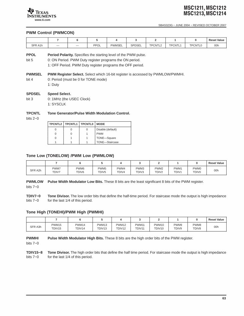
SBAS323G − JUNE 2004 − REVISED OCTOBER 2007
www.ti.com
63
PWM Control (PWMCON)
7 6 5 4 3 2 1 0 Reset Value
SFR A1h — — PPOL PWMSEL SPDSEL TPCNTL2 TPCNTL1 TPCNTL0 00h
PPOL Period Polarity. Specifies the starting level of the PWM pulse.bit 5 0: ON Period. PWM Duty register programs the ON period.
1: OFF Period. PWM Duty register programs the OFF period.
PWMSEL PWM Register Select. Select which 16-bit register is accessed by PWMLOW/PWMHI.bit 4 0: Period (must be 0 for TONE mode)
1: Duty
SPDSEL Speed Select.bit 3 0: 1MHz (the USEC Clock)
1: SYSCLK
TPCNTL Tone Generator/Pulse Width Modulation Control.bits 2−0
TPCNTL2 TPCNTL1 TPCNTL0 MODE
0 0 0 Disable (default)
0 0 1 PWM
0 1 1 TONE—Square
1 1 1 TONE—Staircase
Tone Low (TONELOW) /PWM Low (PWMLOW)
7 6 5 4 3 2 1 0 Reset Value
SFR A2hPWM7TDIV7
PWM6TDIV6
PWM5TDIV5
PWM4TDIV4
PWM3TDIV3
PWM2TDIV2
PWM1TDIV1
PWM0TDIV0
00h
PWMLOW Pulse Width Modulator Low Bits. These 8 bits are the least significant 8 bits of the PWM register.bits 7−0
TDIV7−0 Tone Divisor. The low order bits that define the half-time period. For staircase mode the output is high impedancebits 7−0 for the last 1/4 of this period.
Tone High (TONEHI)/PWM High (PWMHI)
7 6 5 4 3 2 1 0 Reset Value
SFR A3hPWM15TDIV15
PWM14TDIV14
PWM13TDIV13
PWM12TDIV12
PWM11TDIV11
PWM10TDIV10
PWM9TDIV9
PWM8TDIV8
00h
PWMHI Pulse Width Modulator High Bits. These 8 bits are the high order bits of the PWM register.bits 7−0
TDIV15−8 Tone Divisor. The high order bits that define the half time period. For staircase mode the output is high impedancebits 7−0 for the last 1/4 of this period.
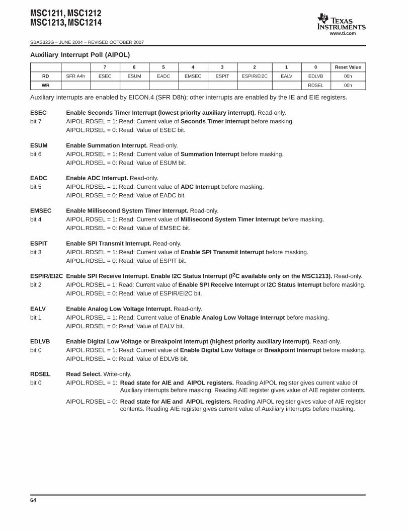
SBAS323G − JUNE 2004 − REVISED OCTOBER 2007
www.ti.com
64
Auxiliary Interrupt Poll (AIPOL)
7 6 5 4 3 2 1 0 Reset Value
RD SFR A4h ESEC ESUM EADC EMSEC ESPIT ESPIR/EI2C EALV EDLVB 00h
WR RDSEL 00h
Auxiliary interrupts are enabled by EICON.4 (SFR D8h); other interrupts are enabled by the IE and EIE registers.
ESEC Enable Seconds Timer Interrupt (lowest priority auxiliary interrupt). Read-only.bit 7 AIPOL.RDSEL = 1: Read: Current value of Seconds T imer Interrupt before masking.
AIPOL.RDSEL = 0: Read: Value of ESEC bit.
ESUM Enable Summation Interrupt. Read-only.bit 6 AIPOL.RDSEL = 1: Read: Current value of Summation Interrupt before masking.
AIPOL.RDSEL = 0: Read: Value of ESUM bit.
EADC Enable ADC Interrupt. Read-only.bit 5 AIPOL.RDSEL = 1: Read: Current value of ADC Interrupt before masking.
AIPOL.RDSEL = 0: Read: Value of EADC bit.
EMSEC Enable Millisecond System Timer Interrupt. Read-only.bit 4 AIPOL.RDSEL = 1: Read: Current value of Millisecond System T imer Interrupt before masking.
AIPOL.RDSEL = 0: Read: Value of EMSEC bit.
ESPIT Enable SPI Transmit Interrupt. Read-only.bit 3 AIPOL.RDSEL = 1: Read: Current value of Enable SPI Transmit Interrupt before masking.
AIPOL.RDSEL = 0: Read: Value of ESPIT bit.
ESPIR/EI2C Enable SPI Receive Interrupt. Enable I2C Status Interrupt (I 2C available only on the MSC1213). Read-only.bit 2 AIPOL.RDSEL = 1: Read: Current value of Enable SPI Receive Interrupt or I2C Status Interrupt before masking.
AIPOL.RDSEL = 0: Read: Value of ESPIR/EI2C bit.
EALV Enable Analog Low Voltage Interrupt. Read-only.bit 1 AIPOL.RDSEL = 1: Read: Current value of Enable Analog Low Voltage Interrupt before masking.
AIPOL.RDSEL = 0: Read: Value of EALV bit.
EDLVB Enable Digital Low Voltage or Breakpoint Interrupt (highest priority auxiliary interrupt). Read-only.bit 0 AIPOL.RDSEL = 1: Read: Current value of Enable Digital Low Voltage or Breakpoint Interrupt before masking.
AIPOL.RDSEL = 0: Read: Value of EDLVB bit.
RDSEL Read Select. Write-only.bit 0 AIPOL.RDSEL = 1: Read state for AIE and AIPOL registers. Reading AIPOL register gives current value of
Auxiliary interrupts before masking. Reading AIE register gives value of AIE register contents.
AIPOL.RDSEL = 0: Read state for AIE and AIPOL registers. Reading AIPOL register gives value of AIE registercontents. Reading AIE register gives current value of Auxiliary interrupts before masking.
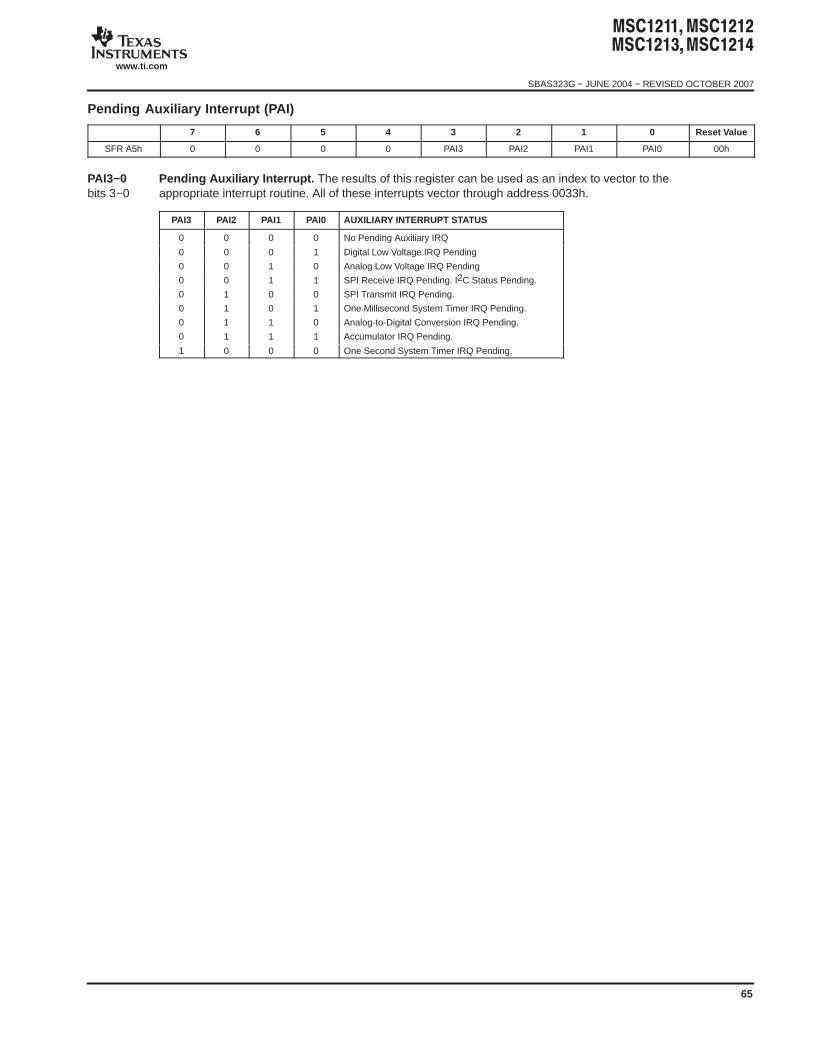
SBAS323G − JUNE 2004 − REVISED OCTOBER 2007
www.ti.com
65
Pending Auxiliary Interrupt (PAI)
7 6 5 4 3 2 1 0 Reset Value
SFR A5h 0 0 0 0 PAI3 PAI2 PAI1 PAI0 00h
PAI3−0 Pending Auxiliary Interrupt. The results of this register can be used as an index to vector to thebits 3−0 appropriate interrupt routine. All of these interrupts vector through address 0033h.
PAI3 PAI2 PAI1 PAI0 AUXILIARY INTERRUPT STATUS
0 0 0 0 No Pending Auxiliary IRQ
0 0 0 1 Digital Low Voltage IRQ Pending
0 0 1 0 Analog Low Voltage IRQ Pending
0 0 1 1 SPI Receive IRQ Pending. I2C Status Pending.
0 1 0 0 SPI Transmit IRQ Pending.
0 1 0 1 One Millisecond System Timer IRQ Pending.
0 1 1 0 Analog-to-Digital Conversion IRQ Pending.
0 1 1 1 Accumulator IRQ Pending.
1 0 0 0 One Second System Timer IRQ Pending.
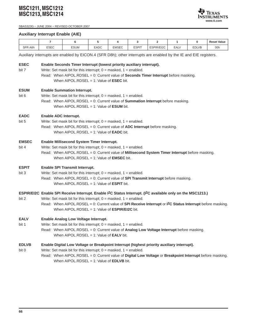
SBAS323G − JUNE 2004 − REVISED OCTOBER 2007
www.ti.com
66
Auxiliary Interrupt Enable (AIE)
7 6 5 4 3 2 1 0 Reset Value
SFR A6h ESEC ESUM EADC EMSEC ESPIT ESPIR/EI2C EALV EDLVB 00h
Auxiliary interrupts are enabled by EICON.4 (SFR D8h); other interrupts are enabled by the IE and EIE registers.
ESEC Enable Seconds Timer Interrupt (lowest priority auxiliary interrupt).bit 7 Write: Set mask bit for this interrupt; 0 = masked, 1 = enabled.
Read: When AIPOL.RDSEL = 0: Current value of Seconds T imer Interrupt before masking.When AIPOL.RDSEL = 1: Value of ESEC bit.
ESUM Enable Summation Interrupt.bit 6 Write: Set mask bit for this interrupt; 0 = masked, 1 = enabled.
Read: When AIPOL.RDSEL = 0: Current value of Summation Interrupt before masking.When AIPOL.RDSEL = 1: Value of ESUM bit.
EADC Enable ADC Interrupt.bit 5 Write: Set mask bit for this interrupt; 0 = masked, 1 = enabled.
Read: When AIPOL.RDSEL = 0: Current value of ADC Interrupt before masking.When AIPOL.RDSEL = 1: Value of EADC bit.
EMSEC Enable Millisecond System Timer Interrupt.bit 4 Write: Set mask bit for this interrupt; 0 = masked, 1 = enabled.
Read: When AIPOL.RDSEL = 0: Current value of Millisecond System T imer Interrupt before masking.When AIPOL.RDSEL = 1: Value of EMSEC bit.
ESPIT Enable SPI Transmit Interrupt.bit 3 Write: Set mask bit for this interrupt; 0 = masked, 1 = enabled.
Read: When AIPOL.RDSEL = 0: Current value of SPI Transmit Interrupt before masking.When AIPOL.RDSEL = 1: Value of ESPIT bit.
ESPIR/EI2C Enable SPI Receive Interrupt. Enable I 2C Status Interrupt. (I 2C available only on the MSC1213.)bit 2 Write: Set mask bit for this interrupt; 0 = masked, 1 = enabled.
Read: When AIPOL.RDSEL = 0: Current value of SPI Receive Interrupt or I2C Status Interrupt before masking.When AIPOL.RDSEL = 1: Value of ESPIR/EI2C bit.
EALV Enable Analog Low Voltage Interrupt.bit 1 Write: Set mask bit for this interrupt; 0 = masked, 1 = enabled.
Read: When AIPOL.RDSEL = 0: Current value of Analog Low Voltage Interrupt before masking.When AIPOL.RDSEL = 1: Value of EALV bit.
EDLVB Enable Digital Low Voltage or Breakpoint Interrupt (highest priority auxiliary interrupt).bit 0 Write: Set mask bit for this interrupt; 0 = masked, 1 = enabled.
Read: When AIPOL.RDSEL = 0: Current value of Digital Low Voltage or Breakpoint Interrupt before masking.When AIPOL.RDSEL = 1: Value of EDLVB bit.
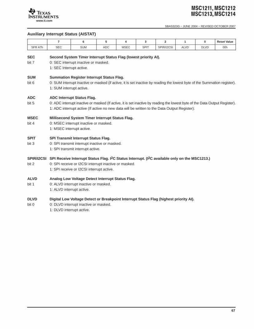
SBAS323G − JUNE 2004 − REVISED OCTOBER 2007
www.ti.com
67
Auxiliary Interrupt Status (AISTAT)
7 6 5 4 3 2 1 0 Reset Value
SFR A7h SEC SUM ADC MSEC SPIT SPIR/I2CSI ALVD DLVD 00h
SEC Second System Timer Interrupt Status Flag (lowest priority AI).bit 7 0: SEC interrupt inactive or masked.
1: SEC Interrupt active.
SUM Summation Register Interrupt Status Flag.bit 6 0: SUM interrupt inactive or masked (if active, it is set inactive by reading the lowest byte of the Summation register).
1: SUM interrupt active.
ADC ADC Interrupt Status Flag.bit 5 0: ADC interrupt inactive or masked (If active, it is set inactive by reading the lowest byte of the Data Output Register).
1: ADC interrupt active (If active no new data will be written to the Data Output Register).
MSEC Millisecond System Timer Interrupt Status Flag.bit 4 0: MSEC interrupt inactive or masked.
1: MSEC interrupt active.
SPIT SPI Transmit Interrupt Status Flag.bit 3 0: SPI transmit interrupt inactive or masked.
1: SPI transmit interrupt active.
SPIR/I2CSI SPI Receive Interrupt Status Flag. I 2C Status Interrupt. (I 2C available only on the MSC1213.)bit 2 0: SPI receive or I2CSI interrupt inactive or masked.
1: SPI receive or I2CSI interrupt active.
ALVD Analog Low Voltage Detect Interrupt Status Flag.bit 1 0: ALVD interrupt inactive or masked.
1: ALVD interrupt active.
DLVD Digital Low Voltage Detect or Breakpoint Interrupt Status Flag (highest priority AI).bit 0 0: DLVD interrupt inactive or masked.
1: DLVD interrupt active.
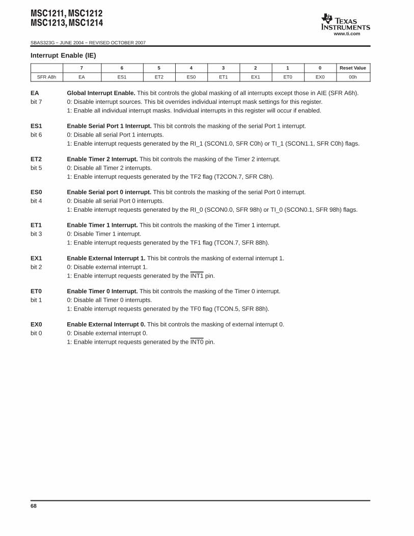
SBAS323G − JUNE 2004 − REVISED OCTOBER 2007
www.ti.com
68
Interrupt Enable (IE)
7 6 5 4 3 2 1 0 Reset Value
SFR A8h EA ES1 ET2 ES0 ET1 EX1 ET0 EX0 00h
EA Global Interrupt Enable. This bit controls the global masking of all interrupts except those in AIE (SFR A6h).bit 7 0: Disable interrupt sources. This bit overrides individual interrupt mask settings for this register.
1: Enable all individual interrupt masks. Individual interrupts in this register will occur if enabled.
ES1 Enable Serial Port 1 Interrupt. This bit controls the masking of the serial Port 1 interrupt.bit 6 0: Disable all serial Port 1 interrupts.
1: Enable interrupt requests generated by the RI_1 (SCON1.0, SFR C0h) or TI_1 (SCON1.1, SFR C0h) flags.
ET2 Enable T imer 2 Interrupt. This bit controls the masking of the Timer 2 interrupt.bit 5 0: Disable all Timer 2 interrupts.
1: Enable interrupt requests generated by the TF2 flag (T2CON.7, SFR C8h).
ES0 Enable Serial port 0 interrupt. This bit controls the masking of the serial Port 0 interrupt.bit 4 0: Disable all serial Port 0 interrupts.
1: Enable interrupt requests generated by the RI_0 (SCON0.0, SFR 98h) or TI_0 (SCON0.1, SFR 98h) flags.
ET1 Enable T imer 1 Interrupt. This bit controls the masking of the Timer 1 interrupt.bit 3 0: Disable Timer 1 interrupt.
1: Enable interrupt requests generated by the TF1 flag (TCON.7, SFR 88h).
EX1 Enable External Interrupt 1. This bit controls the masking of external interrupt 1.bit 2 0: Disable external interrupt 1.
1: Enable interrupt requests generated by the INT1 pin.
ET0 Enable T imer 0 Interrupt. This bit controls the masking of the Timer 0 interrupt.bit 1 0: Disable all Timer 0 interrupts.
1: Enable interrupt requests generated by the TF0 flag (TCON.5, SFR 88h).
EX0 Enable External Interrupt 0. This bit controls the masking of external interrupt 0.bit 0 0: Disable external interrupt 0.
1: Enable interrupt requests generated by the INT0 pin.
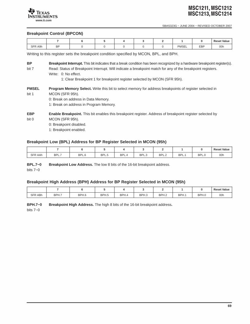
SBAS323G − JUNE 2004 − REVISED OCTOBER 2007
www.ti.com
69
Breakpoint Control (BPCON)
7 6 5 4 3 2 1 0 Reset Value
SFR A9h BP 0 0 0 0 0 PMSEL EBP 00h
Writing to this register sets the breakpoint condition specified by MCON, BPL, and BPH.
BP Breakpoint Interrupt. This bit indicates that a break condition has been recognized by a hardware breakpoint register(s).bit 7 Read: Status of Breakpoint Interrupt. Will indicate a breakpoint match for any of the breakpoint registers.
Write: 0: No effect.1: Clear Breakpoint 1 for breakpoint register selected by MCON (SFR 95h).
PMSEL Program Memory Select. Write this bit to select memory for address breakpoints of register selected inbit 1 MCON (SFR 95h).
0: Break on address in Data Memory.1: Break on address in Program Memory.
EBP Enable Breakpoint. This bit enables this breakpoint register. Address of breakpoint register selected bybit 0 MCON (SFR 95h).
0: Breakpoint disabled.1: Breakpoint enabled.
Breakpoint Low (BPL) Address for BP Register Selected in MCON (95h)
7 6 5 4 3 2 1 0 Reset Value
SFR AAh BPL.7 BPL.6 BPL.5 BPL.4 BPL.3 BPL.2 BPL.1 BPL.0 00h
BPL.7−0 Breakpoint Low Address. The low 8 bits of the 16-bit breakpoint address.bits 7−0
Breakpoint High Address (BPH) Address for BP Register Selected in MCON (95h)
7 6 5 4 3 2 1 0 Reset Value
SFR ABh BPH.7 BPH.6 BPH.5 BPH.4 BPH.3 BPH.2 BPH.1 BPH.0 00h
BPH.7−0 Breakpoint High Address. The high 8 bits of the 16-bit breakpoint address.bits 7−0
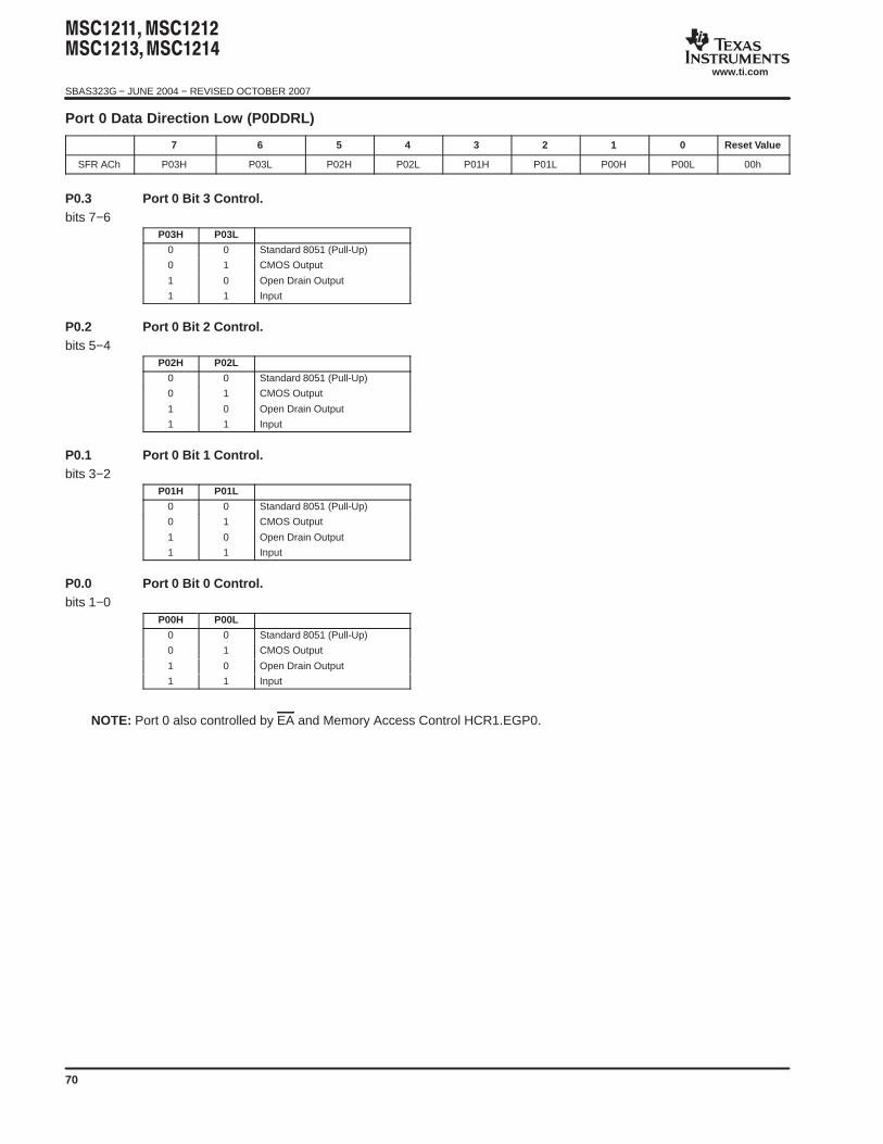
SBAS323G − JUNE 2004 − REVISED OCTOBER 2007
www.ti.com
70
Port 0 Data Direction Low (P0DDRL)
7 6 5 4 3 2 1 0 Reset Value
SFR ACh P03H P03L P02H P02L P01H P01L P00H P00L 00h
P0.3 Port 0 Bit 3 Control.bits 7−6
P03H P03L
0 0 Standard 8051 (Pull-Up)
0 1 CMOS Output
1 0 Open Drain Output
1 1 Input
P0.2 Port 0 Bit 2 Control.bits 5−4
P02H P02L
0 0 Standard 8051 (Pull-Up)
0 1 CMOS Output
1 0 Open Drain Output
1 1 Input
P0.1 Port 0 Bit 1 Control.bits 3−2
P01H P01L
0 0 Standard 8051 (Pull-Up)
0 1 CMOS Output
1 0 Open Drain Output
1 1 Input
P0.0 Port 0 Bit 0 Control.bits 1−0
P00H P00L
0 0 Standard 8051 (Pull-Up)
0 1 CMOS Output
1 0 Open Drain Output
1 1 Input
NOTE: Port 0 also controlled by EA and Memory Access Control HCR1.EGP0.

SBAS323G − JUNE 2004 − REVISED OCTOBER 2007
www.ti.com
71
Port 0 Data Direction High (P0DDRH)
7 6 5 4 3 2 1 0 Reset Value
SFR ADh P07H P07L P06H P06L P05H P05L P04H P04L 00h
P0.7 Port 0 Bit 7 Control.bits 7−6
P07H P07L
0 0 Standard 8051 (Pull-Up)
0 1 CMOS Output
1 0 Open Drain Output
1 1 Input
P0.6 Port 0 Bit 6 Control.bits 5−4
P06H P06L
0 0 Standard 8051 (Pull-Up)
0 1 CMOS Output
1 0 Open Drain Output
1 1 Input
P0.5 Port 0 Bit 5 Control.bits 3−2
P05H P05L
0 0 Standard 8051 (Pull-Up)
0 1 CMOS Output
1 0 Open Drain Output
1 1 Input
P0.4 Port 0 Bit 4 Control.bits 1−0
P04H P04L
0 0 Standard 8051 (Pull-Up)
0 1 CMOS Output
1 0 Open Drain Output
1 1 Input
NOTE: Port 0 also controlled by EA and Memory Access Control HCR1.EGP0.
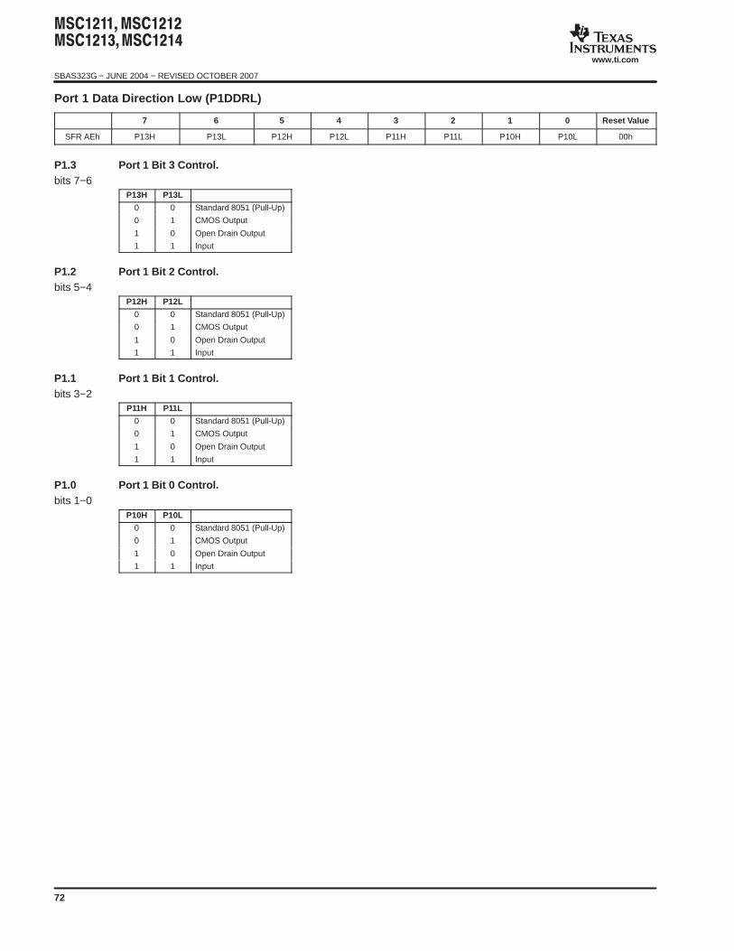
SBAS323G − JUNE 2004 − REVISED OCTOBER 2007
www.ti.com
72
Port 1 Data Direction Low (P1DDRL)
7 6 5 4 3 2 1 0 Reset Value
SFR AEh P13H P13L P12H P12L P11H P11L P10H P10L 00h
P1.3 Port 1 Bit 3 Control.bits 7−6
P13H P13L
0 0 Standard 8051 (Pull-Up)
0 1 CMOS Output
1 0 Open Drain Output
1 1 Input
P1.2 Port 1 Bit 2 Control.bits 5−4
P12H P12L
0 0 Standard 8051 (Pull-Up)
0 1 CMOS Output
1 0 Open Drain Output
1 1 Input
P1.1 Port 1 Bit 1 Control.bits 3−2
P11H P11L
0 0 Standard 8051 (Pull-Up)
0 1 CMOS Output
1 0 Open Drain Output
1 1 Input
P1.0 Port 1 Bit 0 Control.bits 1−0
P10H P10L
0 0 Standard 8051 (Pull-Up)
0 1 CMOS Output
1 0 Open Drain Output
1 1 Input
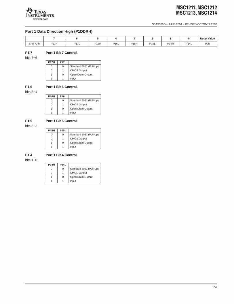
SBAS323G − JUNE 2004 − REVISED OCTOBER 2007
www.ti.com
73
Port 1 Data Direction High (P1DDRH)
7 6 5 4 3 2 1 0 Reset Value
SFR AFh P17H P17L P16H P16L P15H P15L P14H P14L 00h
P1.7 Port 1 Bit 7 Control.bits 7−6
P17H P17L
0 0 Standard 8051 (Pull-Up)
0 1 CMOS Output
1 0 Open Drain Output
1 1 Input
P1.6 Port 1 Bit 6 Control.bits 5−4
P16H P16L
0 0 Standard 8051 (Pull-Up)
0 1 CMOS Output
1 0 Open Drain Output
1 1 Input
P1.5 Port 1 Bit 5 Control.bits 3−2
P15H P15L
0 0 Standard 8051 (Pull-Up)
0 1 CMOS Output
1 0 Open Drain Output
1 1 Input
P1.4 Port 1 Bit 4 Control.bits 1−0
P14H P14L
0 0 Standard 8051 (Pull-Up)
0 1 CMOS Output
1 0 Open Drain Output
1 1 Input
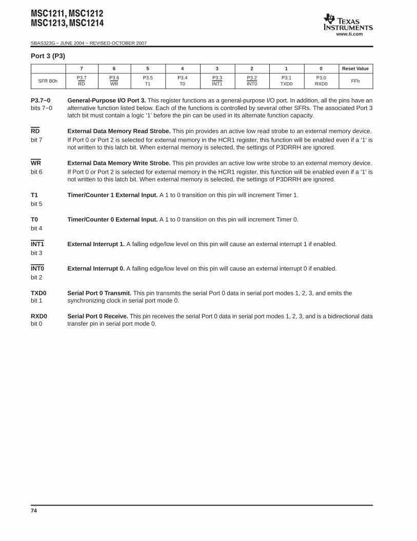
SBAS323G − JUNE 2004 − REVISED OCTOBER 2007
www.ti.com
74
Port 3 (P3)
7 6 5 4 3 2 1 0 Reset Value
SFR B0hP3.7RD
P3.6WR
P3.5T1
P3.4T0
P3.3INT1
P3.2INT0
P3.1TXD0
P3.0RXD0
FFh
P3.7−0 General-Purpose I/O Port 3. This register functions as a general-purpose I/O port. In addition, all the pins have anbits 7−0 alternative function listed below. Each of the functions is controlled by several other SFRs. The associated Port 3
latch bit must contain a logic ‘1’ before the pin can be used in its alternate function capacity.
RD External Data Memory Read Strobe. This pin provides an active low read strobe to an external memory device.bit 7 If Port 0 or Port 2 is selected for external memory in the HCR1 register, this function will be enabled even if a ‘1’ is
not written to this latch bit. When external memory is selected, the settings of P3DRRH are ignored.
WR External Data Memory Write Strobe. This pin provides an active low write strobe to an external memory device.bit 6 If Port 0 or Port 2 is selected for external memory in the HCR1 register, this function will be enabled even if a ‘1’ is
not written to this latch bit. When external memory is selected, the settings of P3DRRH are ignored.
T1 Timer/Counter 1 External Input. A 1 to 0 transition on this pin will increment Timer 1.bit 5
T0 Timer/Counter 0 External Input. A 1 to 0 transition on this pin will increment Timer 0.bit 4
INT1 External Interrupt 1. A falling edge/low level on this pin will cause an external interrupt 1 if enabled.bit 3
INT0 External Interrupt 0. A falling edge/low level on this pin will cause an external interrupt 0 if enabled.bit 2
TXD0 Serial Port 0 Transmit. This pin transmits the serial Port 0 data in serial port modes 1, 2, 3, and emits thebit 1 synchronizing clock in serial port mode 0.
RXD0 Serial Port 0 Receive. This pin receives the serial Port 0 data in serial port modes 1, 2, 3, and is a bidirectional databit 0 transfer pin in serial port mode 0.
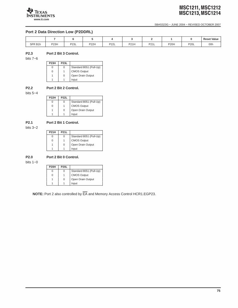
SBAS323G − JUNE 2004 − REVISED OCTOBER 2007
www.ti.com
75
Port 2 Data Direction Low (P2DDRL)
7 6 5 4 3 2 1 0 Reset Value
SFR B1h P23H P23L P22H P22L P21H P21L P20H P20L 00h
P2.3 Port 2 Bit 3 Control.bits 7−6
P23H P23L
0 0 Standard 8051 (Pull-Up)
0 1 CMOS Output
1 0 Open Drain Output
1 1 Input
P2.2 Port 2 Bit 2 Control.bits 5−4
P22H P22L
0 0 Standard 8051 (Pull-Up)
0 1 CMOS Output
1 0 Open Drain Output
1 1 Input
P2.1 Port 2 Bit 1 Control.bits 3−2
P21H P21L
0 0 Standard 8051 (Pull-Up)
0 1 CMOS Output
1 0 Open Drain Output
1 1 Input
P2.0 Port 2 Bit 0 Control.bits 1−0
P20H P20L
0 0 Standard 8051 (Pull-Up)
0 1 CMOS Output
1 0 Open Drain Output
1 1 Input
NOTE: Port 2 also controlled by EA and Memory Access Control HCR1.EGP23.
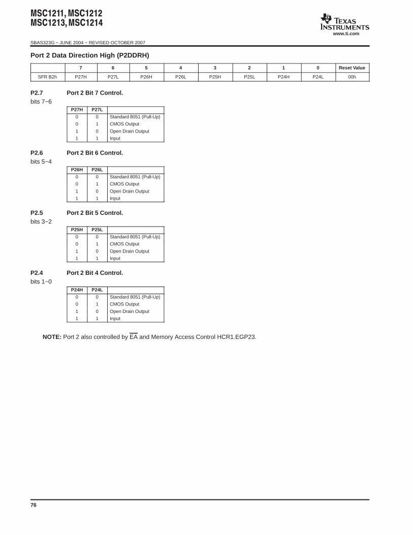
SBAS323G − JUNE 2004 − REVISED OCTOBER 2007
www.ti.com
76
Port 2 Data Direction High (P2DDRH)
7 6 5 4 3 2 1 0 Reset Value
SFR B2h P27H P27L P26H P26L P25H P25L P24H P24L 00h
P2.7 Port 2 Bit 7 Control.bits 7−6
P27H P27L
0 0 Standard 8051 (Pull-Up)
0 1 CMOS Output
1 0 Open Drain Output
1 1 Input
P2.6 Port 2 Bit 6 Control.bits 5−4
P26H P26L
0 0 Standard 8051 (Pull-Up)
0 1 CMOS Output
1 0 Open Drain Output
1 1 Input
P2.5 Port 2 Bit 5 Control.bits 3−2
P25H P25L
0 0 Standard 8051 (Pull-Up)
0 1 CMOS Output
1 0 Open Drain Output
1 1 Input
P2.4 Port 2 Bit 4 Control.bits 1−0
P24H P24L
0 0 Standard 8051 (Pull-Up)
0 1 CMOS Output
1 0 Open Drain Output
1 1 Input
NOTE: Port 2 also controlled by EA and Memory Access Control HCR1.EGP23.

SBAS323G − JUNE 2004 − REVISED OCTOBER 2007
www.ti.com
77
Port 3 Data Direction Low (P3DDRL)
7 6 5 4 3 2 1 0 Reset Value
SFR B3h P33H P33L P32H P32L P31H P31L P30H P30L 00h
P3.3 Port 3 Bit 3 Control.bits 7−6
P33H P33L
0 0 Standard 8051 (Pull-Up)
0 1 CMOS Output
1 0 Open Drain Output
1 1 Input
P3.2 Port 3 Bit 2 Control.bits 5−4
P32H P32L
0 0 Standard 8051 (Pull-Up)
0 1 CMOS Output
1 0 Open Drain Output
1 1 Input
P3.1 Port 3 Bit 1 Control.bits 3−2
P31H P31L
0 0 Standard 8051 (Pull-Up)
0 1 CMOS Output
1 0 Open Drain Output
1 1 Input
P3.0 Port 3 Bit 0 Control.bits 1−0
P30H P30L
0 0 Standard 8051 (Pull-Up)
0 1 CMOS Output
1 0 Open Drain Output
1 1 Input
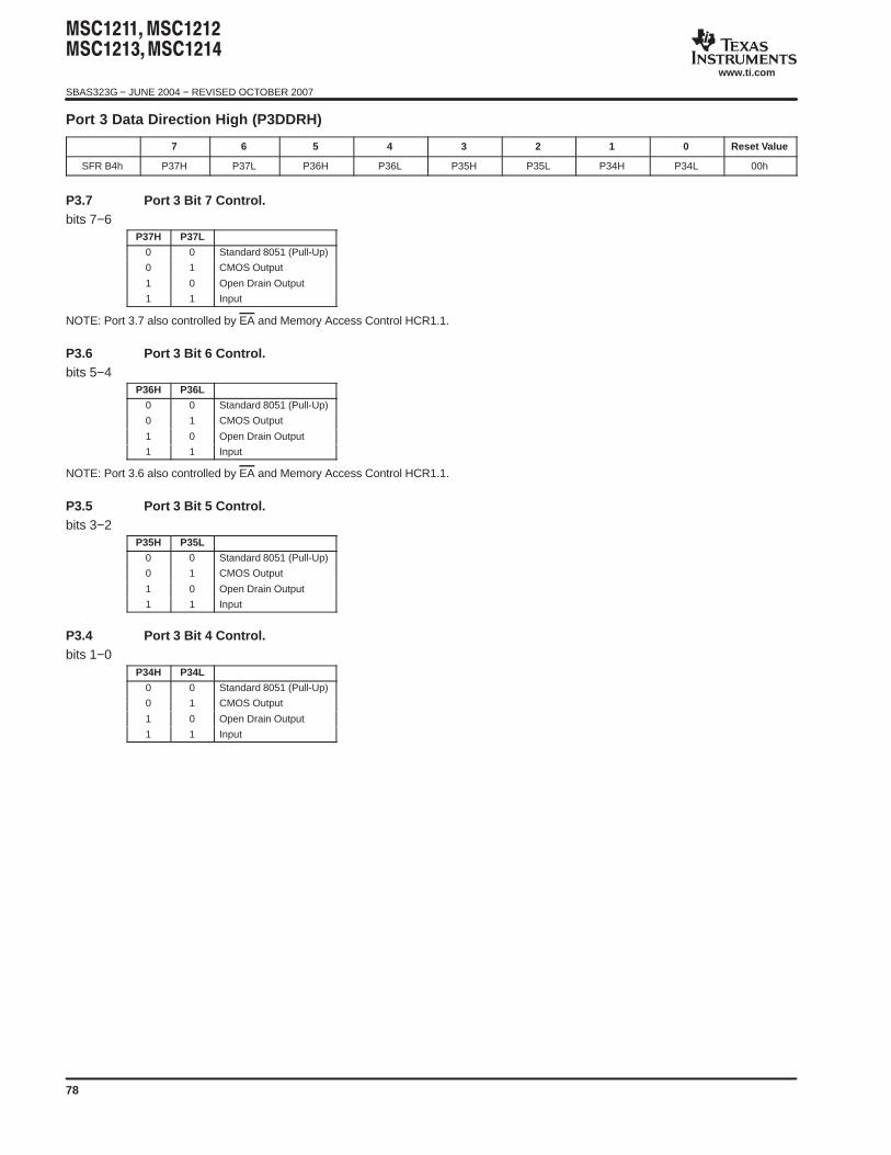
SBAS323G − JUNE 2004 − REVISED OCTOBER 2007
www.ti.com
78
Port 3 Data Direction High (P3DDRH)
7 6 5 4 3 2 1 0 Reset Value
SFR B4h P37H P37L P36H P36L P35H P35L P34H P34L 00h
P3.7 Port 3 Bit 7 Control.bits 7−6
P37H P37L
0 0 Standard 8051 (Pull-Up)
0 1 CMOS Output
1 0 Open Drain Output
1 1 Input
NOTE: Port 3.7 also controlled by EA and Memory Access Control HCR1.1.
P3.6 Port 3 Bit 6 Control.bits 5−4
P36H P36L
0 0 Standard 8051 (Pull-Up)
0 1 CMOS Output
1 0 Open Drain Output
1 1 Input
NOTE: Port 3.6 also controlled by EA and Memory Access Control HCR1.1.
P3.5 Port 3 Bit 5 Control.bits 3−2
P35H P35L
0 0 Standard 8051 (Pull-Up)
0 1 CMOS Output
1 0 Open Drain Output
1 1 Input
P3.4 Port 3 Bit 4 Control.bits 1−0
P34H P34L
0 0 Standard 8051 (Pull-Up)
0 1 CMOS Output
1 0 Open Drain Output
1 1 Input
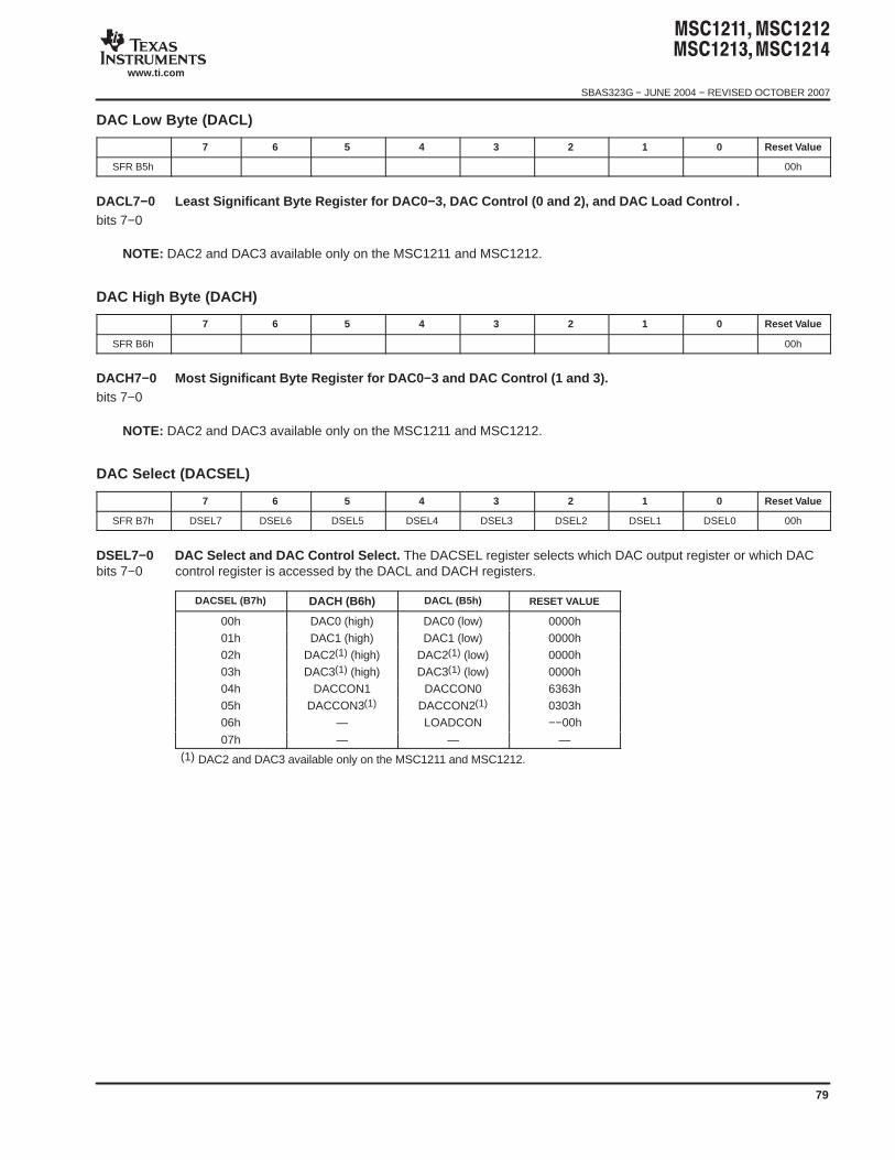
SBAS323G − JUNE 2004 − REVISED OCTOBER 2007
www.ti.com
79
DAC Low Byte (DACL)
7 6 5 4 3 2 1 0 Reset Value
SFR B5h 00h
DACL7−0 Least Significant Byte Register for DAC0−3, DAC Control (0 and 2), and DAC Load Control .bits 7−0
NOTE: DAC2 and DAC3 available only on the MSC1211 and MSC1212.
DAC High Byte (DACH)
7 6 5 4 3 2 1 0 Reset Value
SFR B6h 00h
DACH7−0 Most Significant Byte Register for DAC0−3 and DAC Control (1 and 3).bits 7−0
NOTE: DAC2 and DAC3 available only on the MSC1211 and MSC1212.
DAC Select (DACSEL)
7 6 5 4 3 2 1 0 Reset Value
SFR B7h DSEL7 DSEL6 DSEL5 DSEL4 DSEL3 DSEL2 DSEL1 DSEL0 00h
DSEL7−0 DAC Select and DAC Control Select. The DACSEL register selects which DAC output register or which DACbits 7−0 control register is accessed by the DACL and DACH registers.
DACSEL (B7h) DACH (B6h) DACL (B5h) RESET VALUE
00h DAC0 (high) DAC0 (low) 0000h01h DAC1 (high) DAC1 (low) 0000h02h DAC2(1) (high) DAC2(1) (low) 0000h03h DAC3(1) (high) DAC3(1) (low) 0000h04h DACCON1 DACCON0 6363h05h DACCON3(1) DACCON2(1) 0303h06h — LOADCON −−00h
07h — — —(1) DAC2 and DAC3 available only on the MSC1211 and MSC1212.
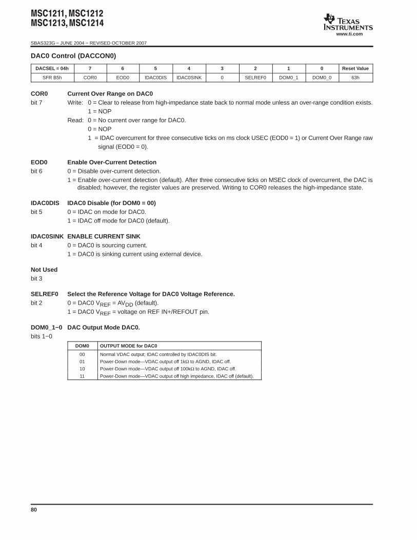
SBAS323G − JUNE 2004 − REVISED OCTOBER 2007
www.ti.com
80
DAC0 Control (DACCON0)
DACSEL = 04h 7 6 5 4 3 2 1 0 Reset Value
SFR B5h COR0 EOD0 IDAC0DIS IDAC0SINK 0 SELREF0 DOM0_1 DOM0_0 63h
COR0 Current Over Range on DAC0bit 7 Write: 0 = Clear to release from high-impedance state back to normal mode unless an over-range condition exists.
1 = NOPRead: 0 = No current over range for DAC0.
0 = NOP1 = IDAC overcurrent for three consecutive ticks on ms clock USEC (EOD0 = 1) or Current Over Range raw
signal (EOD0 = 0).
EOD0 Enable Over-Current Detectionbit 6 0 = Disable over-current detection.
1 = Enable over-current detection (default). After three consecutive ticks on MSEC clock of overcurrent, the DAC is disabled; however, the register values are preserved. Writing to COR0 releases the high-impedance state.
IDAC0DIS IDAC0 Disable (for DOM0 = 00)bit 5 0 = IDAC on mode for DAC0.
1 = IDAC off mode for DAC0 (default).
IDAC0SINK ENABLE CURRENT SINKbit 4 0 = DAC0 is sourcing current.
1 = DAC0 is sinking current using external device.
Not Usedbit 3
SELREF0 Select the Reference Voltage for DAC0 Voltage Reference.bit 2 0 = DAC0 VREF = AVDD (default).
1 = DAC0 VREF = voltage on REF IN+/REFOUT pin.
DOM0_1−0 DAC Output Mode DAC0.bits 1−0
DOM0 OUTPUT MODE for DAC0
00 Normal VDAC output; IDAC controlled by IDAC0DIS bit.
01 Power-Down mode—VDAC output off 1kΩ to AGND, IDAC off.
10 Power-Down mode—VDAC output off 100kΩ to AGND, IDAC off.
11 Power-Down mode—VDAC output off high impedance, IDAC off (default).
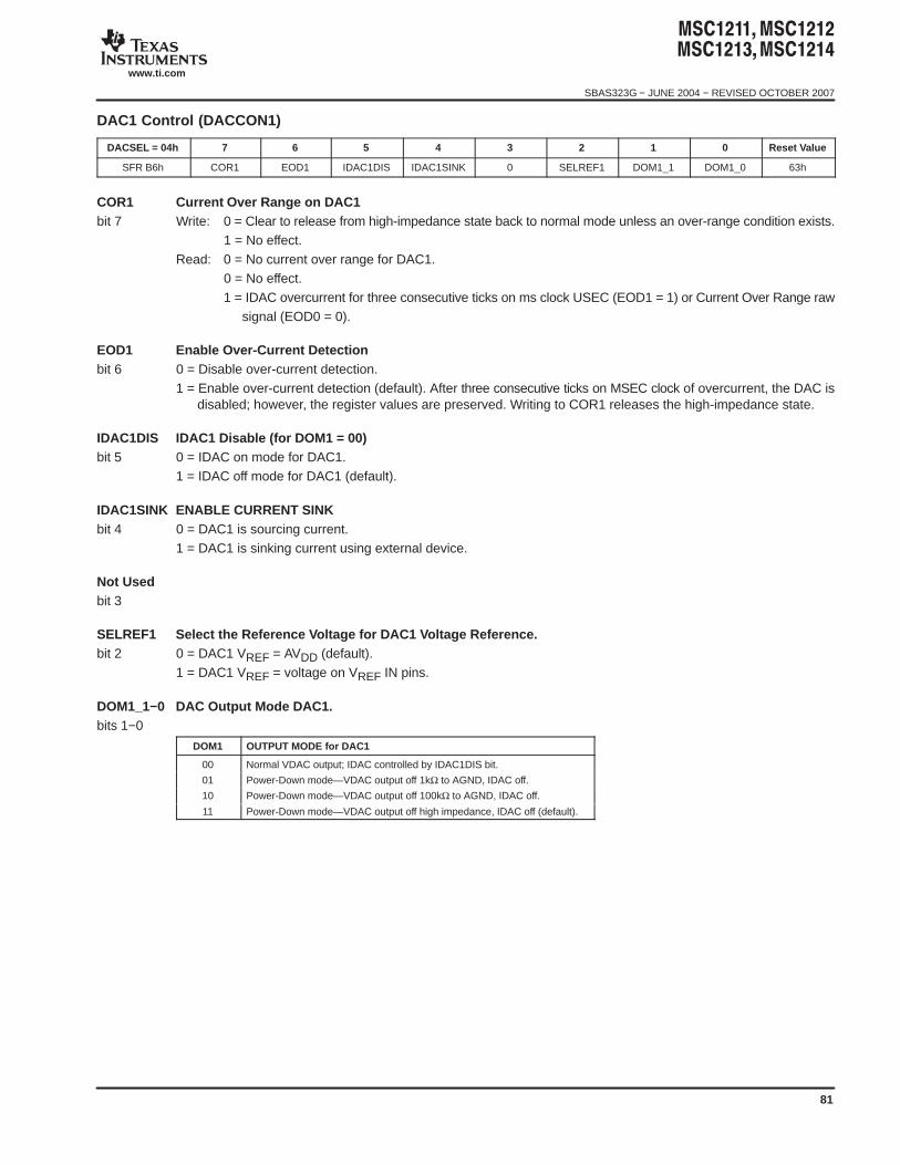
SBAS323G − JUNE 2004 − REVISED OCTOBER 2007
www.ti.com
81
DAC1 Control (DACCON1)
DACSEL = 04h 7 6 5 4 3 2 1 0 Reset Value
SFR B6h COR1 EOD1 IDAC1DIS IDAC1SINK 0 SELREF1 DOM1_1 DOM1_0 63h
COR1 Current Over Range on DAC1bit 7 Write: 0 = Clear to release from high-impedance state back to normal mode unless an over-range condition exists.
1 = No effect.Read: 0 = No current over range for DAC1.
0 = No effect. 1 = IDAC overcurrent for three consecutive ticks on ms clock USEC (EOD1 = 1) or Current Over Range raw
signal (EOD0 = 0).
EOD1 Enable Over-Current Detectionbit 6 0 = Disable over-current detection.
1 = Enable over-current detection (default). After three consecutive ticks on MSEC clock of overcurrent, the DAC is disabled; however, the register values are preserved. Writing to COR1 releases the high-impedance state.
IDAC1DIS IDAC1 Disable (for DOM1 = 00)bit 5 0 = IDAC on mode for DAC1.
1 = IDAC off mode for DAC1 (default).
IDAC1SINK ENABLE CURRENT SINKbit 4 0 = DAC1 is sourcing current.
1 = DAC1 is sinking current using external device.
Not Usedbit 3
SELREF1 Select the Reference Voltage for DAC1 Voltage Reference.bit 2 0 = DAC1 VREF = AVDD (default).
1 = DAC1 VREF = voltage on VREF IN pins.
DOM1_1−0 DAC Output Mode DAC1.bits 1−0
DOM1 OUTPUT MODE for DAC1
00 Normal VDAC output; IDAC controlled by IDAC1DIS bit.
01 Power-Down mode—VDAC output off 1kΩ to AGND, IDAC off.
10 Power-Down mode—VDAC output off 100kΩ to AGND, IDAC off.
11 Power-Down mode—VDAC output off high impedance, IDAC off (default).
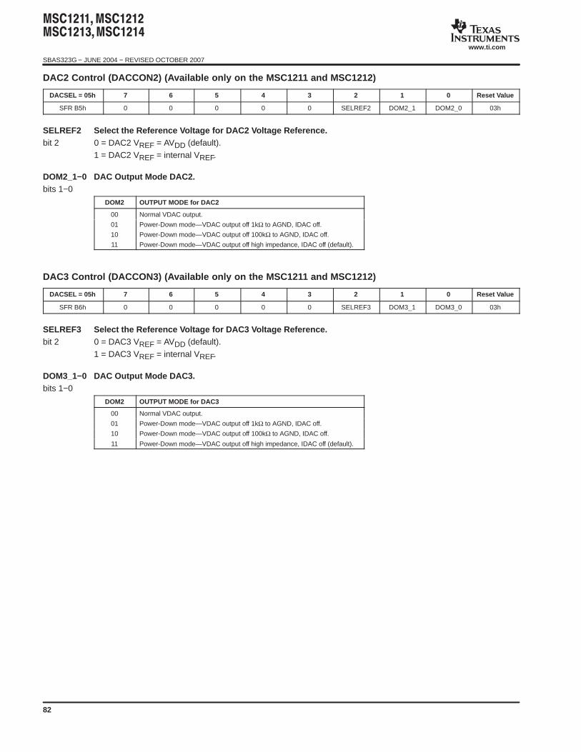
SBAS323G − JUNE 2004 − REVISED OCTOBER 2007
www.ti.com
82
DAC2 Control (DACCON2) (Available only on the MSC1211 and MSC1212)
DACSEL = 05h 7 6 5 4 3 2 1 0 Reset Value
SFR B5h 0 0 0 0 0 SELREF2 DOM2_1 DOM2_0 03h
SELREF2 Select the Reference Voltage for DAC2 Voltage Reference.bit 2 0 = DAC2 VREF = AVDD (default).
1 = DAC2 VREF = internal VREF.
DOM2_1−0 DAC Output Mode DAC2.bits 1−0
DOM2 OUTPUT MODE for DAC2
00 Normal VDAC output.
01 Power-Down mode—VDAC output off 1kΩ to AGND, IDAC off.
10 Power-Down mode—VDAC output off 100kΩ to AGND, IDAC off.
11 Power-Down mode—VDAC output off high impedance, IDAC off (default).
DAC3 Control (DACCON3) (Available only on the MSC1211 and MSC1212)
DACSEL = 05h 7 6 5 4 3 2 1 0 Reset Value
SFR B6h 0 0 0 0 0 SELREF3 DOM3_1 DOM3_0 03h
SELREF3 Select the Reference Voltage for DAC3 Voltage Reference.bit 2 0 = DAC3 VREF = AVDD (default).
1 = DAC3 VREF = internal VREF.
DOM3_1−0 DAC Output Mode DAC3.bits 1−0
DOM2 OUTPUT MODE for DAC3
00 Normal VDAC output.
01 Power-Down mode—VDAC output off 1kΩ to AGND, IDAC off.
10 Power-Down mode—VDAC output off 100kΩ to AGND, IDAC off.
11 Power-Down mode—VDAC output off high impedance, IDAC off (default).
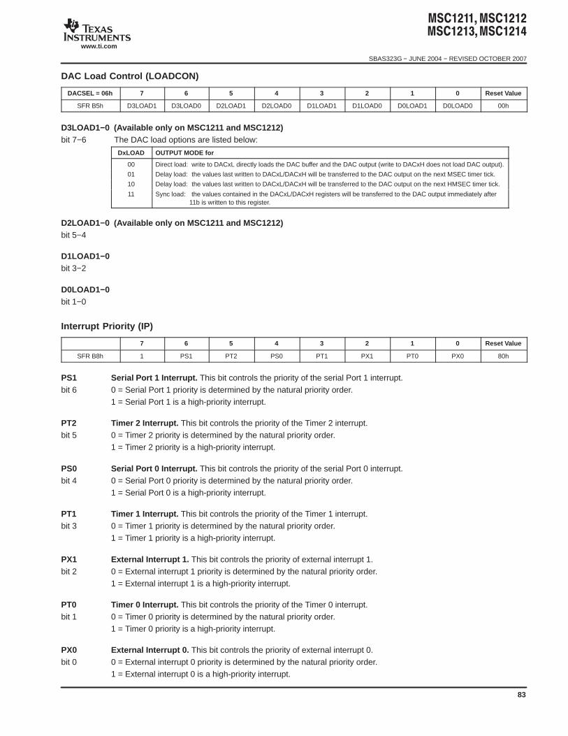
SBAS323G − JUNE 2004 − REVISED OCTOBER 2007
www.ti.com
83
DAC Load Control (LOADCON)
DACSEL = 06h 7 6 5 4 3 2 1 0 Reset Value
SFR B5h D3LOAD1 D3LOAD0 D2LOAD1 D2LOAD0 D1LOAD1 D1LOAD0 D0LOAD1 D0LOAD0 00h
D3LOAD1−0 (Available only on MSC1211 and MSC1212)bit 7−6 The DAC load options are listed below:
DxLOAD OUTPUT MODE for
00 Direct load: write to DACxL directly loads the DAC buffer and the DAC output (write to DACxH does not load DAC output).
01 Delay load: the values last written to DACxL/DACxH will be transferred to the DAC output on the next MSEC timer tick.
10 Delay load: the values last written to DACxL/DACxH will be transferred to the DAC output on the next HMSEC timer tick.
11 Sync load: the values contained in the DACxL/DACxH registers will be transferred to the DAC output immediately after 11b is written to this register.
D2LOAD1−0 (Available only on MSC1211 and MSC1212)bit 5−4
D1LOAD1−0bit 3−2
D0LOAD1−0bit 1−0
Interrupt Priority (IP)
7 6 5 4 3 2 1 0 Reset Value
SFR B8h 1 PS1 PT2 PS0 PT1 PX1 PT0 PX0 80h
PS1 Serial Port 1 Interrupt. This bit controls the priority of the serial Port 1 interrupt.bit 6 0 = Serial Port 1 priority is determined by the natural priority order.
1 = Serial Port 1 is a high-priority interrupt.
PT2 Timer 2 Interrupt. This bit controls the priority of the Timer 2 interrupt.bit 5 0 = Timer 2 priority is determined by the natural priority order.
1 = Timer 2 priority is a high-priority interrupt.
PS0 Serial Port 0 Interrupt. This bit controls the priority of the serial Port 0 interrupt.bit 4 0 = Serial Port 0 priority is determined by the natural priority order.
1 = Serial Port 0 is a high-priority interrupt.
PT1 Timer 1 Interrupt. This bit controls the priority of the Timer 1 interrupt.bit 3 0 = Timer 1 priority is determined by the natural priority order.
1 = Timer 1 priority is a high-priority interrupt.
PX1 External Interrupt 1. This bit controls the priority of external interrupt 1.bit 2 0 = External interrupt 1 priority is determined by the natural priority order.
1 = External interrupt 1 is a high-priority interrupt.
PT0 Timer 0 Interrupt. This bit controls the priority of the Timer 0 interrupt.bit 1 0 = Timer 0 priority is determined by the natural priority order.
1 = Timer 0 priority is a high-priority interrupt.
PX0 External Interrupt 0. This bit controls the priority of external interrupt 0.bit 0 0 = External interrupt 0 priority is determined by the natural priority order.
1 = External interrupt 0 is a high-priority interrupt.
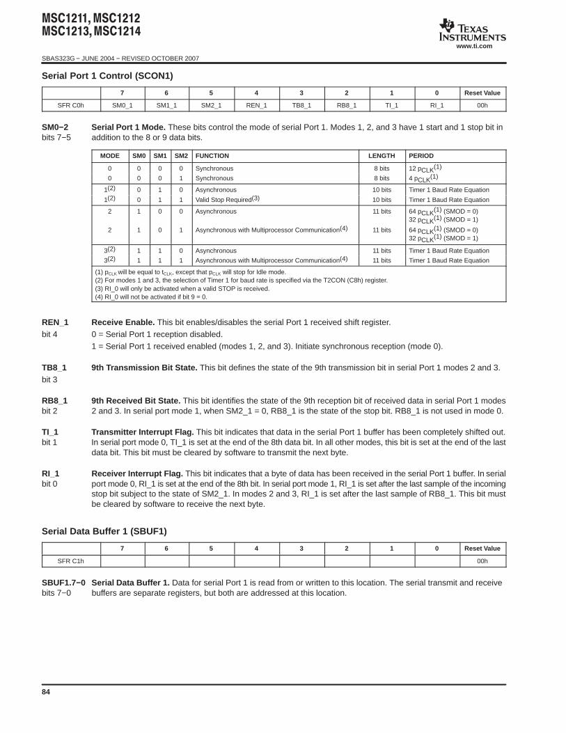
SBAS323G − JUNE 2004 − REVISED OCTOBER 2007
www.ti.com
84
Serial Port 1 Control (SCON1)
7 6 5 4 3 2 1 0 Reset Value
SFR C0h SM0_1 SM1_1 SM2_1 REN_1 TB8_1 RB8_1 TI_1 RI_1 00h
SM0−2 Serial Port 1 Mode. These bits control the mode of serial Port 1. Modes 1, 2, and 3 have 1 start and 1 stop bit inbits 7−5 addition to the 8 or 9 data bits.
MODE SM0 SM1 SM2 FUNCTION LENGTH PERIOD
0 0 0 0 Synchronous 8 bits 12 pCLK(1)
0 0 0 1 Synchronous 8 bits 4 pCLK(1)
1(2) 0 1 0 Asynchronous 10 bits Timer 1 Baud Rate Equation
1(2) 0 1 1 Valid Stop Required(3) 10 bits Timer 1 Baud Rate Equation
2 1 0 0 Asynchronous 11 bits 64 pCLK(1) (SMOD = 0)32 pCLK(1) (SMOD = 1)
2 1 0 1 Asynchronous with Multiprocessor Communication(4) 11 bits 64 pCLK(1) (SMOD = 0)32 pCLK(1) (SMOD = 1)
3(2) 1 1 0 Asynchronous 11 bits Timer 1 Baud Rate Equation
3(2) 1 1 1 Asynchronous with Multiprocessor Communication(4) 11 bits Timer 1 Baud Rate Equation
(1) pCLK will be equal to tCLK, except that pCLK will stop for Idle mode.(2) For modes 1 and 3, the selection of Timer 1 for baud rate is specified via the T2CON (C8h) register.(3) RI_0 will only be activated when a valid STOP is received.(4) RI_0 will not be activated if bit 9 = 0.
REN_1 Receive Enable. This bit enables/disables the serial Port 1 received shift register.bit 4 0 = Serial Port 1 reception disabled.
1 = Serial Port 1 received enabled (modes 1, 2, and 3). Initiate synchronous reception (mode 0).
TB8_1 9th Transmission Bit State. This bit defines the state of the 9th transmission bit in serial Port 1 modes 2 and 3.bit 3
RB8_1 9th Received Bit State. This bit identifies the state of the 9th reception bit of received data in serial Port 1 modesbit 2 2 and 3. In serial port mode 1, when SM2_1 = 0, RB8_1 is the state of the stop bit. RB8_1 is not used in mode 0.
TI_1 Transmitter Interrupt Flag. This bit indicates that data in the serial Port 1 buffer has been completely shifted out.bit 1 In serial port mode 0, TI_1 is set at the end of the 8th data bit. In all other modes, this bit is set at the end of the last
data bit. This bit must be cleared by software to transmit the next byte.
RI_1 Receiver Interrupt Flag. This bit indicates that a byte of data has been received in the serial Port 1 buffer. In serialbit 0 port mode 0, RI_1 is set at the end of the 8th bit. In serial port mode 1, RI_1 is set after the last sample of the incoming
stop bit subject to the state of SM2_1. In modes 2 and 3, RI_1 is set after the last sample of RB8_1. This bit mustbe cleared by software to receive the next byte.
Serial Data Buffer 1 (SBUF1)
7 6 5 4 3 2 1 0 Reset Value
SFR C1h 00h
SBUF1.7−0 Serial Data Buffer 1. Data for serial Port 1 is read from or written to this location. The serial transmit and receivebits 7−0 buffers are separate registers, but both are addressed at this location.
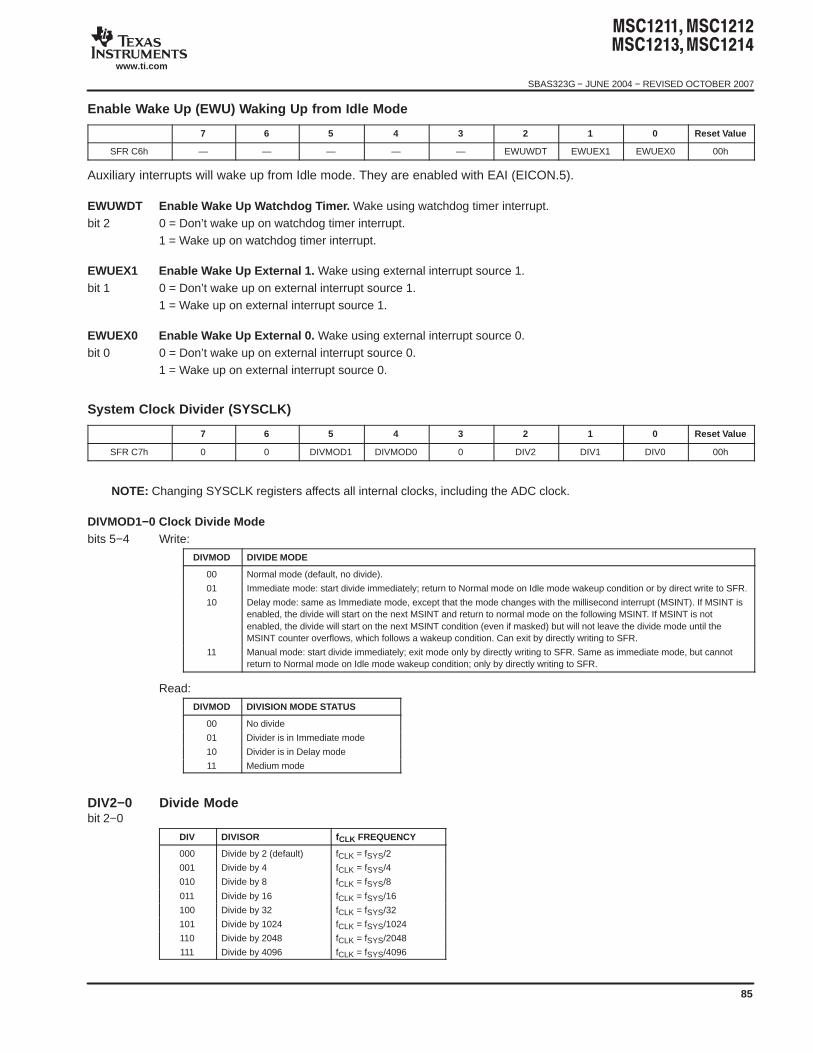
SBAS323G − JUNE 2004 − REVISED OCTOBER 2007
www.ti.com
85
Enable Wake Up (EWU) Waking Up from Idle Mode
7 6 5 4 3 2 1 0 Reset Value
SFR C6h — — — — — EWUWDT EWUEX1 EWUEX0 00h
Auxiliary interrupts will wake up from Idle mode. They are enabled with EAI (EICON.5).
EWUWDT Enable Wake Up Watchdog Timer. Wake using watchdog timer interrupt.bit 2 0 = Don’t wake up on watchdog timer interrupt.
1 = Wake up on watchdog timer interrupt.
EWUEX1 Enable Wake Up External 1. Wake using external interrupt source 1.bit 1 0 = Don’t wake up on external interrupt source 1.
1 = Wake up on external interrupt source 1.
EWUEX0 Enable Wake Up External 0. Wake using external interrupt source 0.bit 0 0 = Don’t wake up on external interrupt source 0.
1 = Wake up on external interrupt source 0.
System Clock Divider (SYSCLK)
7 6 5 4 3 2 1 0 Reset Value
SFR C7h 0 0 DIVMOD1 DIVMOD0 0 DIV2 DIV1 DIV0 00h
NOTE: Changing SYSCLK registers affects all internal clocks, including the ADC clock.
DIVMOD1−0 Clock Divide Modebits 5−4 Write:
DIVMOD DIVIDE MODE
00 Normal mode (default, no divide).
01 Immediate mode: start divide immediately; return to Normal mode on Idle mode wakeup condition or by direct write to SFR.
10 Delay mode: same as Immediate mode, except that the mode changes with the millisecond interrupt (MSINT). If MSINT isenabled, the divide will start on the next MSINT and return to normal mode on the following MSINT. If MSINT is notenabled, the divide will start on the next MSINT condition (even if masked) but will not leave the divide mode until theMSINT counter overflows, which follows a wakeup condition. Can exit by directly writing to SFR.
11 Manual mode: start divide immediately; exit mode only by directly writing to SFR. Same as immediate mode, but cannotreturn to Normal mode on Idle mode wakeup condition; only by directly writing to SFR.
Read:
DIVMOD DIVISION MODE STATUS
00 No divide
01 Divider is in Immediate mode
10 Divider is in Delay mode
11 Medium mode
DIV2−0 Divide Modebit 2−0
DIV DIVISOR fCLK FREQUENCY
000 Divide by 2 (default) fCLK = fSYS/2
001 Divide by 4 fCLK = fSYS/4
010 Divide by 8 fCLK = fSYS/8
011 Divide by 16 fCLK = fSYS/16
100 Divide by 32 fCLK = fSYS/32
101 Divide by 1024 fCLK = fSYS/1024
110 Divide by 2048 fCLK = fSYS/2048
111 Divide by 4096 fCLK = fSYS/4096
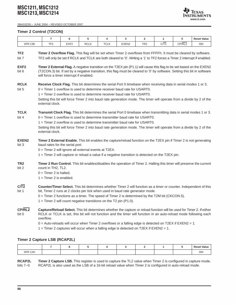
SBAS323G − JUNE 2004 − REVISED OCTOBER 2007
www.ti.com
86
Timer 2 Control (T2CON)
7 6 5 4 3 2 1 0 Reset Value
SFR C8h TF2 EXF2 RCLK TCLK EXEN2 TR2 C/T2 CP/RL2 00h
TF2 Timer 2 Overflow Flag. This flag will be set when Timer 2 overflows from FFFFh. It must be cleared by software.bit 7 TF2 will only be set if RCLK and TCLK are both cleared to ‘0’. Writing a ‘1’ to TF2 forces a Timer 2 interrupt if enabled.
EXF2 Timer 2 External Flag. A negative transition on the T2EX pin (P1.1) will cause this flag to be set based on the EXEN2bit 6 (T2CON.3) bit. If set by a negative transition, this flag must be cleared to ‘0’ by software. Setting this bit in software
will force a timer interrupt if enabled.
RCLK Receive Clock Flag. This bit determines the serial Port 0 timebase when receiving data in serial modes 1 or 3.bit 5 0 = Timer 1 overflow is used to determine receiver baud rate for USART0.
1 = Timer 2 overflow is used to determine receiver baud rate for USART0.Setting this bit will force Timer 2 into baud rate generation mode. The timer will operate from a divide by 2 of theexternal clock.
TCLK Transmit Clock Flag. This bit determines the serial Port 0 timebase when transmitting data in serial modes 1 or 3.bit 4 0 = Timer 1 overflow is used to determine transmitter baud rate for USART0.
1 = Timer 2 overflow is used to determine transmitter baud rate for USART0.Setting this bit will force Timer 2 into baud rate generation mode. The timer will operate from a divide by 2 of theexternal clock.
EXEN2 Timer 2 External Enable. This bit enables the capture/reload function on the T2EX pin if Timer 2 is not generatingbit 3 baud rates for the serial port.
0 = Timer 2 will ignore all external events at T2EX.1 = Timer 2 will capture or reload a value if a negative transition is detected on the T2EX pin.
TR2 Timer 2 Run Control. This bit enables/disables the operation of Timer 2. Halting this timer will preserve the currentbit 2 count in TH2, TL2.
0 = Timer 2 is halted.1 = Timer 2 is enabled.
C/T2 Counter/Timer Select. This bit determines whether Timer 2 will function as a timer or counter. Independent of thisbit 1 bit, Timer 2 runs at 2 clocks per tick when used in baud rate generator mode.
0 = Timer 2 functions as a timer. The speed of Timer 2 is determined by the T2M bit (CKCON.5).1 = Timer 2 will count negative transitions on the T2 pin (P1.0).
CP/RL2 Capture/Reload Select. This bit determines whether the capture or reload function will be used for Timer 2. If eitherbit 0 RCLK or TCLK is set, this bit will not function and the timer will function in an auto-reload mode following each
overflow.0 = Auto-reloads will occur when Timer 2 overflows or a falling edge is detected on T2EX if EXEN2 = 1.1 = Timer 2 captures will occur when a falling edge is detected on T2EX if EXEN2 = 1.
Timer 2 Capture LSB (RCAP2L)
7 6 5 4 3 2 1 0 Reset Value
SFR CAh 00h
RCAP2L Timer 2 Capture LSB. This register is used to capture the TL2 value when Timer 2 is configured in capture mode.bits 7−0 RCAP2L is also used as the LSB of a 16-bit reload value when Timer 2 is configured in auto-reload mode.
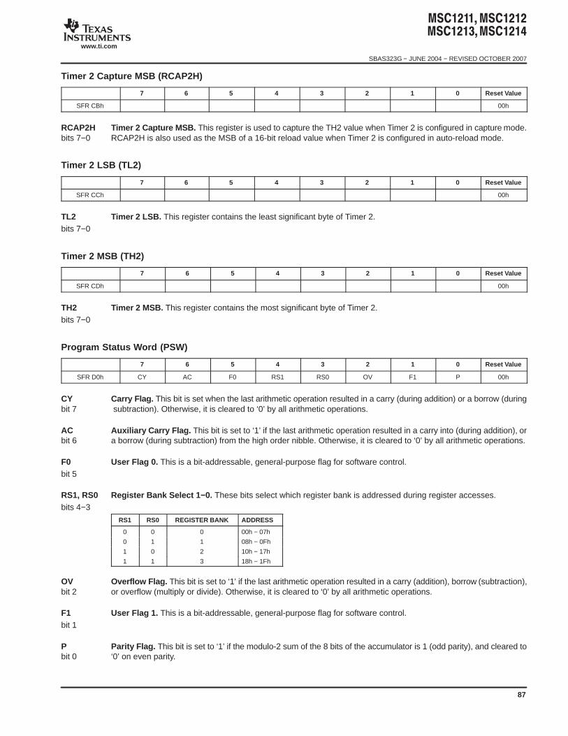
SBAS323G − JUNE 2004 − REVISED OCTOBER 2007
www.ti.com
87
Timer 2 Capture MSB (RCAP2H)
7 6 5 4 3 2 1 0 Reset Value
SFR CBh 00h
RCAP2H Timer 2 Capture MSB. This register is used to capture the TH2 value when Timer 2 is configured in capture mode.bits 7−0 RCAP2H is also used as the MSB of a 16-bit reload value when Timer 2 is configured in auto-reload mode.
Timer 2 LSB (TL2)
7 6 5 4 3 2 1 0 Reset Value
SFR CCh 00h
TL2 Timer 2 LSB. This register contains the least significant byte of Timer 2.bits 7−0
Timer 2 MSB (TH2)
7 6 5 4 3 2 1 0 Reset Value
SFR CDh 00h
TH2 Timer 2 MSB. This register contains the most significant byte of Timer 2.bits 7−0
Program Status Word (PSW)
7 6 5 4 3 2 1 0 Reset Value
SFR D0h CY AC F0 RS1 RS0 OV F1 P 00h
CY Carry Flag. This bit is set when the last arithmetic operation resulted in a carry (during addition) or a borrow (duringbit 7 subtraction). Otherwise, it is cleared to ‘0’ by all arithmetic operations.
AC Auxiliary Carry Flag. This bit is set to ‘1’ if the last arithmetic operation resulted in a carry into (during addition), orbit 6 a borrow (during subtraction) from the high order nibble. Otherwise, it is cleared to ‘0’ by all arithmetic operations.
F0 User Flag 0. This is a bit-addressable, general-purpose flag for software control.bit 5
RS1, RS0 Register Bank Select 1−0. These bits select which register bank is addressed during register accesses.bits 4−3
RS1 RS0 REGISTER BANK ADDRESS
0 0 0 00h − 07h
0 1 1 08h − 0Fh
1 0 2 10h − 17h
1 1 3 18h − 1Fh
OV Overflow Flag. This bit is set to ‘1’ if the last arithmetic operation resulted in a carry (addition), borrow (subtraction),bit 2 or overflow (multiply or divide). Otherwise, it is cleared to ‘0’ by all arithmetic operations.
F1 User Flag 1. This is a bit-addressable, general-purpose flag for software control.bit 1
P Parity Flag. This bit is set to ‘1’ if the modulo-2 sum of the 8 bits of the accumulator is 1 (odd parity), and cleared tobit 0 ‘0’ on even parity.
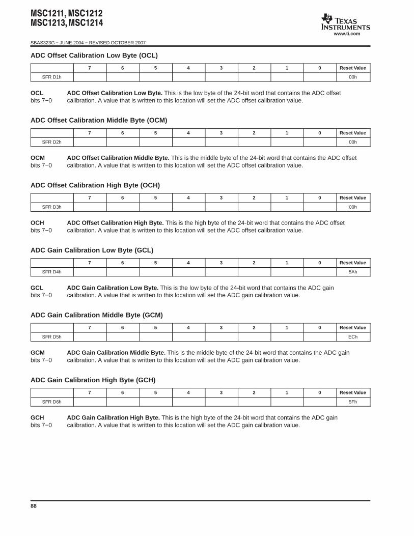
SBAS323G − JUNE 2004 − REVISED OCTOBER 2007
www.ti.com
88
ADC Offset Calibration Low Byte (OCL)
7 6 5 4 3 2 1 0 Reset Value
SFR D1h 00h
OCL ADC Offset Calibration Low Byte. This is the low byte of the 24-bit word that contains the ADC offsetbits 7−0 calibration. A value that is written to this location will set the ADC offset calibration value.
ADC Offset Calibration Middle Byte (OCM)
7 6 5 4 3 2 1 0 Reset Value
SFR D2h 00h
OCM ADC Offset Calibration Middle Byte. This is the middle byte of the 24-bit word that contains the ADC offsetbits 7−0 calibration. A value that is written to this location will set the ADC offset calibration value.
ADC Offset Calibration High Byte (OCH)
7 6 5 4 3 2 1 0 Reset Value
SFR D3h 00h
OCH ADC Offset Calibration High Byte. This is the high byte of the 24-bit word that contains the ADC offsetbits 7−0 calibration. A value that is written to this location will set the ADC offset calibration value.
ADC Gain Calibration Low Byte (GCL)
7 6 5 4 3 2 1 0 Reset Value
SFR D4h 5Ah
GCL ADC Gain Calibration Low Byte. This is the low byte of the 24-bit word that contains the ADC gainbits 7−0 calibration. A value that is written to this location will set the ADC gain calibration value.
ADC Gain Calibration Middle Byte (GCM)
7 6 5 4 3 2 1 0 Reset Value
SFR D5h ECh
GCM ADC Gain Calibration Middle Byte. This is the middle byte of the 24-bit word that contains the ADC gainbits 7−0 calibration. A value that is written to this location will set the ADC gain calibration value.
ADC Gain Calibration High Byte (GCH)
7 6 5 4 3 2 1 0 Reset Value
SFR D6h 5Fh
GCH ADC Gain Calibration High Byte. This is the high byte of the 24-bit word that contains the ADC gainbits 7−0 calibration. A value that is written to this location will set the ADC gain calibration value.
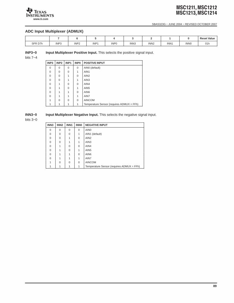
SBAS323G − JUNE 2004 − REVISED OCTOBER 2007
www.ti.com
89
ADC Input Multiplexer (ADMUX)
7 6 5 4 3 2 1 0 Reset Value
SFR D7h INP3 INP2 INP1 INP0 INN3 INN2 INN1 INN0 01h
INP3−0 Input Multiplexer Positive Input. This selects the positive signal input.bits 7−4
INP3 INP2 INP1 INP0 POSITIVE INPUT
0 0 0 0 AIN0 (default)
0 0 0 1 AIN1
0 0 1 0 AIN2
0 0 1 1 AIN3
0 1 0 0 AIN4
0 1 0 1 AIN5
0 1 1 0 AIN6
0 1 1 1 AIN7
1 0 0 0 AINCOM
1 1 1 1 Temperature Sensor (requires ADMUX = FFh)
INN3−0 Input Multiplexer Negative Input. This selects the negative signal input.bits 3−0
INN3 INN2 INN1 INN0 NEGATIVE INPUT
0 0 0 0 AIN0
0 0 0 1 AIN1 (default)
0 0 1 0 AIN2
0 0 1 1 AIN3
0 1 0 0 AIN4
0 1 0 1 AIN5
0 1 1 0 AIN6
0 1 1 1 AIN7
1 0 0 0 AINCOM
1 1 1 1 Temperature Sensor (requires ADMUX = FFh)
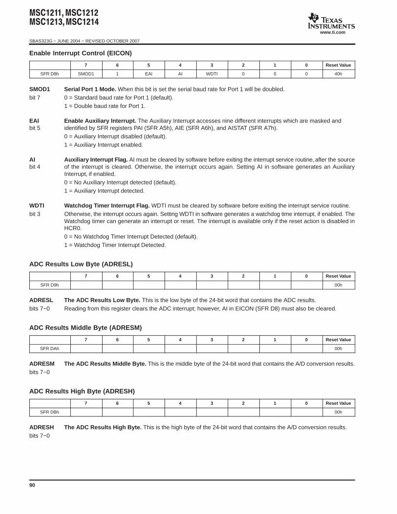
SBAS323G − JUNE 2004 − REVISED OCTOBER 2007
www.ti.com
90
Enable Interrupt Control (EICON)
7 6 5 4 3 2 1 0 Reset Value
SFR D8h SMOD1 1 EAI AI WDTI 0 0 0 40h
SMOD1 Serial Port 1 Mode. When this bit is set the serial baud rate for Port 1 will be doubled.bit 7 0 = Standard baud rate for Port 1 (default).
1 = Double baud rate for Port 1.
EAI Enable Auxiliary Interrupt. The Auxiliary Interrupt accesses nine different interrupts which are masked andbit 5 identified by SFR registers PAI (SFR A5h), AIE (SFR A6h), and AISTAT (SFR A7h).
0 = Auxiliary Interrupt disabled (default).1 = Auxiliary Interrupt enabled.
AI Auxiliary Interrupt Flag. AI must be cleared by software before exiting the interrupt service routine, after the sourcebit 4 of the interrupt is cleared. Otherwise, the interrupt occurs again. Setting AI in software generates an Auxiliary
Interrupt, if enabled.0 = No Auxiliary Interrupt detected (default).1 = Auxiliary Interrupt detected.
WDTI Watchdog T imer Interrupt Flag. WDTI must be cleared by software before exiting the interrupt service routine. bit 3 Otherwise, the interrupt occurs again. Setting WDTI in software generates a watchdog time interrupt, if enabled. The
Watchdog timer can generate an interrupt or reset. The interrupt is available only if the reset action is disabled inHCR0.0 = No Watchdog Timer Interrupt Detected (default).1 = Watchdog Timer Interrupt Detected.
ADC Results Low Byte (ADRESL)
7 6 5 4 3 2 1 0 Reset Value
SFR D9h 00h
ADRESL The ADC Results Low Byte. This is the low byte of the 24-bit word that contains the ADC results.bits 7−0 Reading from this register clears the ADC interrupt; however, AI in EICON (SFR D8) must also be cleared.
ADC Results Middle Byte (ADRESM)
7 6 5 4 3 2 1 0 Reset Value
SFR DAh 00h
ADRESM The ADC Results Middle Byte. This is the middle byte of the 24-bit word that contains the A/D conversion results.bits 7−0
ADC Results High Byte (ADRESH)
7 6 5 4 3 2 1 0 Reset Value
SFR DBh 00h
ADRESH The ADC Results High Byte. This is the high byte of the 24-bit word that contains the A/D conversion results.bits 7−0
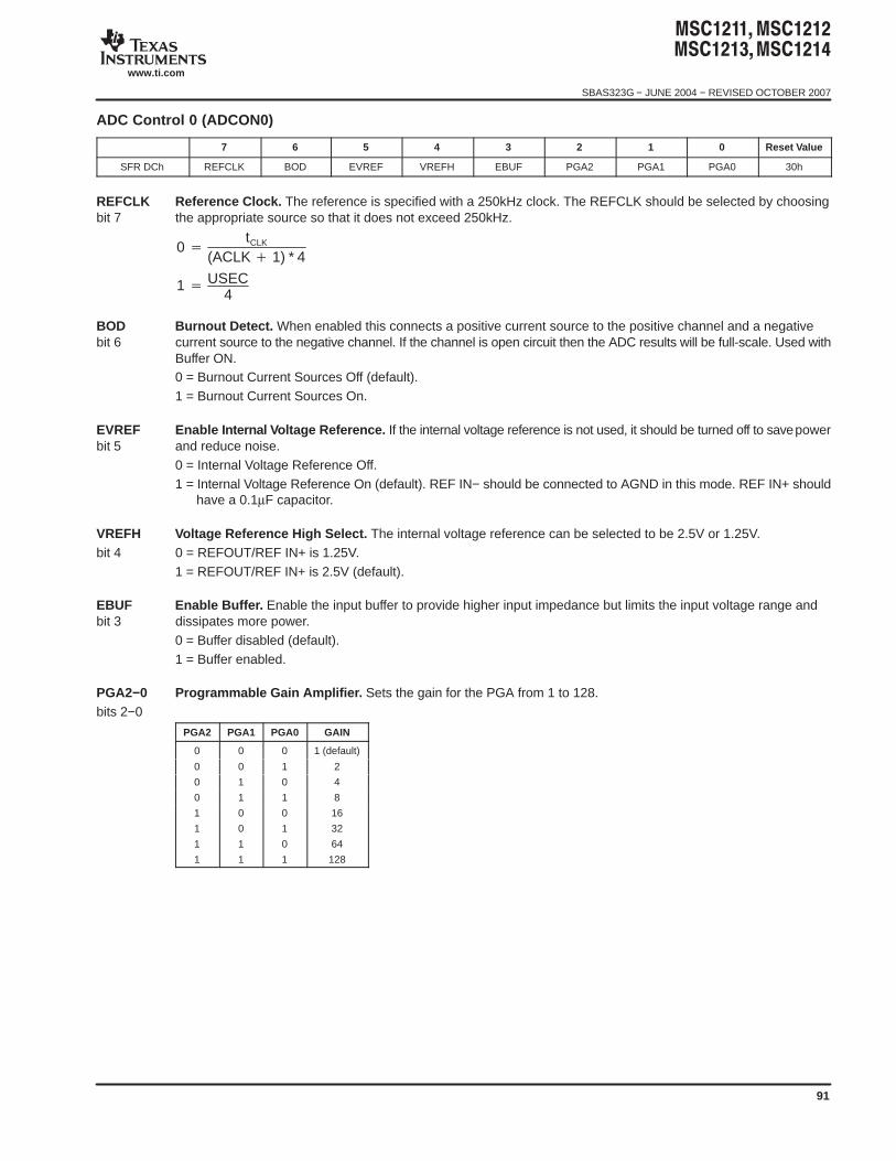
SBAS323G − JUNE 2004 − REVISED OCTOBER 2007
www.ti.com
91
ADC Control 0 (ADCON0)
7 6 5 4 3 2 1 0 Reset Value
SFR DCh REFCLK BOD EVREF VREFH EBUF PGA2 PGA1 PGA0 30h
REFCLK Reference Clock. The reference is specified with a 250kHz clock. The REFCLK should be selected by choosingbit 7 the appropriate source so that it does not exceed 250kHz.
0 tCLK
(ACLK 1) * 4
1 USEC4
BOD Burnout Detect. When enabled this connects a positive current source to the positive channel and a negativebit 6 current source to the negative channel. If the channel is open circuit then the ADC results will be full-scale. Used with
Buffer ON.0 = Burnout Current Sources Off (default).1 = Burnout Current Sources On.
EVREF Enable Internal V oltage Reference. If the internal voltage reference is not used, it should be turned off to save powerbit 5 and reduce noise.
0 = Internal Voltage Reference Off.1 = Internal Voltage Reference On (default). REF IN− should be connected to AGND in this mode. REF IN+ should
have a 0.1µF capacitor.
VREFH Voltage Reference High Select. The internal voltage reference can be selected to be 2.5V or 1.25V.bit 4 0 = REFOUT/REF IN+ is 1.25V.
1 = REFOUT/REF IN+ is 2.5V (default).
EBUF Enable Buffer. Enable the input buffer to provide higher input impedance but limits the input voltage range andbit 3 dissipates more power.
0 = Buffer disabled (default).1 = Buffer enabled.
PGA2−0 Programmable Gain Amplifier. Sets the gain for the PGA from 1 to 128.bits 2−0
PGA2 PGA1 PGA0 GAIN
0 0 0 1 (default)
0 0 1 2
0 1 0 4
0 1 1 8
1 0 0 16
1 0 1 32
1 1 0 64
1 1 1 128
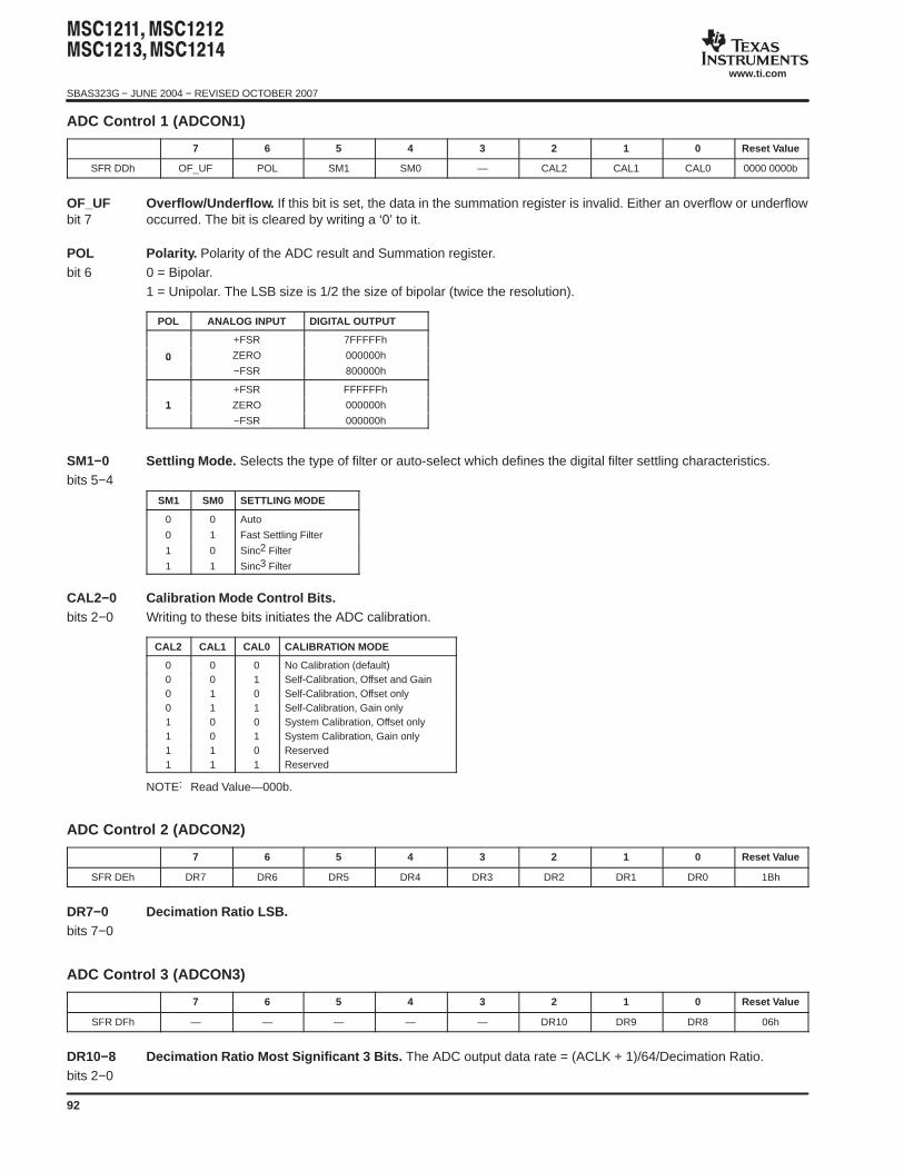
SBAS323G − JUNE 2004 − REVISED OCTOBER 2007
www.ti.com
92
ADC Control 1 (ADCON1)
7 6 5 4 3 2 1 0 Reset Value
SFR DDh OF_UF POL SM1 SM0 — CAL2 CAL1 CAL0 0000 0000b
OF_UF Overflow/Underflow. If this bit is set, the data in the summation register is invalid. Either an overflow or underflowbit 7 occurred. The bit is cleared by writing a ‘0’ to it.
POL Polarity. Polarity of the ADC result and Summation register.bit 6 0 = Bipolar.
1 = Unipolar. The LSB size is 1/2 the size of bipolar (twice the resolution).
POL ANALOG INPUT DIGITAL OUTPUT
+FSR 7FFFFFh
0 ZERO 000000h0−FSR 800000h
+FSR FFFFFFh
1 ZERO 000000h1
−FSR 000000h
SM1−0 Settling Mode. Selects the type of filter or auto-select which defines the digital filter settling characteristics.bits 5−4
SM1 SM0 SETTLING MODE
0 0 Auto
0 1 Fast Settling Filter
1 0 Sinc2 Filter
1 1 Sinc3 Filter
CAL2−0 Calibration Mode Control Bits.bits 2−0 Writing to these bits initiates the ADC calibration.
CAL2 CAL1 CAL0 CALIBRATION MODE
0 0 0 No Calibration (default)0 0 1 Self-Calibration, Offset and Gain0 1 0 Self-Calibration, Offset only0 1 1 Self-Calibration, Gain only1 0 0 System Calibration, Offset only1 0 1 System Calibration, Gain only1 1 0 Reserved1 1 1 Reserved
NOTE: Read Value—000b.
ADC Control 2 (ADCON2)
7 6 5 4 3 2 1 0 Reset Value
SFR DEh DR7 DR6 DR5 DR4 DR3 DR2 DR1 DR0 1Bh
DR7−0 Decimation Ratio LSB.bits 7−0
ADC Control 3 (ADCON3)
7 6 5 4 3 2 1 0 Reset Value
SFR DFh — — — — — DR10 DR9 DR8 06h
DR10−8 Decimation Ratio Most Significant 3 Bits. The ADC output data rate = (ACLK + 1)/64/Decimation Ratio.bits 2−0
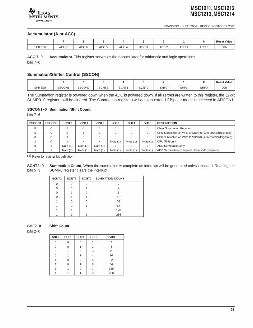
SBAS323G − JUNE 2004 − REVISED OCTOBER 2007
www.ti.com
93
Accumulator (A or ACC)
7 6 5 4 3 2 1 0 Reset Value
SFR E0h ACC.7 ACC.6 ACC.5 ACC.4 ACC.3 ACC.2 ACC.1 ACC.0 00h
ACC.7−0 Accumulator. This register serves as the accumulator for arithmetic and logic operations.bits 7−0
Summation/Shifter Control (SSCON)
7 6 5 4 3 2 1 0 Reset Value
SFR E1h SSCON1 SSCON0 SCNT2 SCNT1 SCNT0 SHF2 SHF1 SHF0 00h
The Summation register is powered down when the ADC is powered down. If all zeroes are written to this register, the 32-bitSUMR3−0 registers will be cleared. The Summation registers will do sign-extend if Bipolar mode is selected in ADCON1.
SSCON1−0 Summation/Shift Count.bits 7−6
SSCON1 SSCON0 SCNT2 SCNT1 SCNT0 SHF2 SHF1 SHF0 DESCRIPTION
0 0 0 0 0 0 0 0 Clear Summation Register
0 0 0 1 0 0 0 0 CPU Summation on Write to SUMR0 (sum count/shift ignored)
0 0 1 0 0 0 0 0 CPU Subtraction on Write to SUMR0 (sum count/shift ignored)
1 0 x x x Note (1) Note (1) Note (1) CPU Shift only
0 1 Note (1) Note (1) Note (1) x x x ADC Summation only
1 1 Note (1) Note (1) Note (1) Note (1) Note (1) Note (1) ADC Summation completes, then shift completes
(1) Refer to register bit definition.
SCNT2−0 Summation Count. When the summation is complete an interrupt will be generated unless masked. Reading thebits 5−3 SUMR0 register clears the interrupt.
SCNT2 SCNT1 SCNT0 SUMMATION COUNT
0 0 0 2
0 0 1 4
0 1 0 8
0 1 1 16
1 0 0 32
1 0 1 64
1 1 0 128
1 1 1 256
SHF2−0 Shift Count.bits 2−0
SHF2 SHF1 SHF0 SHIFT DIVIDE
0 0 0 1 2
0 0 1 2 4
0 1 0 3 8
0 1 1 4 16
1 0 0 5 32
1 0 1 6 64
1 1 0 7 128
1 1 1 8 256
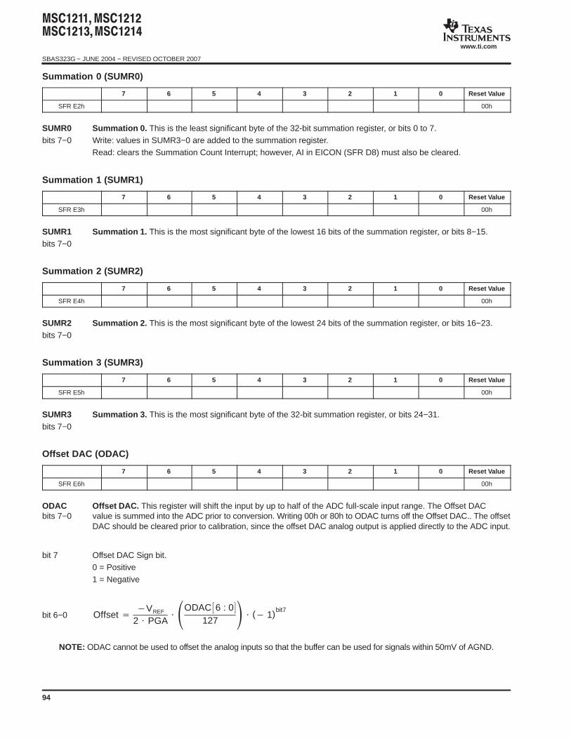
SBAS323G − JUNE 2004 − REVISED OCTOBER 2007
www.ti.com
94
Summation 0 (SUMR0)
7 6 5 4 3 2 1 0 Reset Value
SFR E2h 00h
SUMR0 Summation 0. This is the least significant byte of the 32-bit summation register, or bits 0 to 7.bits 7−0 Write: values in SUMR3−0 are added to the summation register.
Read: clears the Summation Count Interrupt; however, AI in EICON (SFR D8) must also be cleared.
Summation 1 (SUMR1)
7 6 5 4 3 2 1 0 Reset Value
SFR E3h 00h
SUMR1 Summation 1. This is the most significant byte of the lowest 16 bits of the summation register, or bits 8−15.bits 7−0
Summation 2 (SUMR2)
7 6 5 4 3 2 1 0 Reset Value
SFR E4h 00h
SUMR2 Summation 2. This is the most significant byte of the lowest 24 bits of the summation register, or bits 16−23.bits 7−0
Summation 3 (SUMR3)
7 6 5 4 3 2 1 0 Reset Value
SFR E5h 00h
SUMR3 Summation 3. This is the most significant byte of the 32-bit summation register, or bits 24−31.bits 7−0
Offset DAC (ODAC)
7 6 5 4 3 2 1 0 Reset Value
SFR E6h 00h
ODAC Offset DAC. This register will shift the input by up to half of the ADC full-scale input range. The Offset DACbits 7−0 value is summed into the ADC prior to conversion. Writing 00h or 80h to ODAC turns off the Offset DAC.. The offset
DAC should be cleared prior to calibration, since the offset DAC analog output is applied directly to the ADC input.
bit 7 Offset DAC Sign bit.0 = Positive1 = Negative
bit 6−0 Offset VREF
2 PGA ODAC 6 : 0
127 ( 1)bit7
NOTE: ODAC cannot be used to offset the analog inputs so that the buffer can be used for signals within 50mV of AGND.
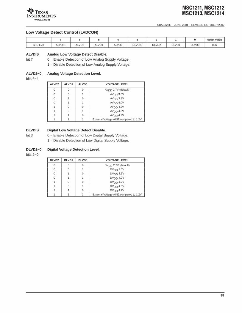
SBAS323G − JUNE 2004 − REVISED OCTOBER 2007
www.ti.com
95
Low Voltage Detect Control (LVDCON)
7 6 5 4 3 2 1 0 Reset Value
SFR E7h ALVDIS ALVD2 ALVD1 ALVD0 DLVDIS DLVD2 DLVD1 DLVD0 00h
ALVDIS Analog Low Voltage Detect Disable.bit 7 0 = Enable Detection of Low Analog Supply Voltage.
1 = Disable Detection of Low Analog Supply Voltage.
ALVD2−0 Analog Voltage Detection Level.bits 6−4
ALVD2 ALVD1 ALVD0 VOLTAGE LEVEL
0 0 0 AVDD 2.7V (default)
0 0 1 AVDD 3.0V
0 1 0 AVDD 3.3V
0 1 1 AVDD 4.0V
1 0 0 AVDD 4.2V
1 0 1 AVDD 4.5V
1 1 0 AVDD 4.7V
1 1 1 External Voltage AIN7 compared to 1.2V
DLVDIS Digital Low Voltage Detect Disable.bit 3 0 = Enable Detection of Low Digital Supply Voltage.
1 = Disable Detection of Low Digital Supply Voltage.
DLVD2−0 Digital Voltage Detection Level.bits 2−0
DLVD2 DLVD1 DLVD0 VOLTAGE LEVEL
0 0 0 DVDD 2.7V (default)
0 0 1 DVDD 3.0V
0 1 0 DVDD 3.3V
0 1 1 DVDD 4.0V
1 0 0 DVDD 4.2V
1 0 1 DVDD 4.5V
1 1 0 DVDD 4.7V
1 1 1 External Voltage AIN6 compared to 1.2V
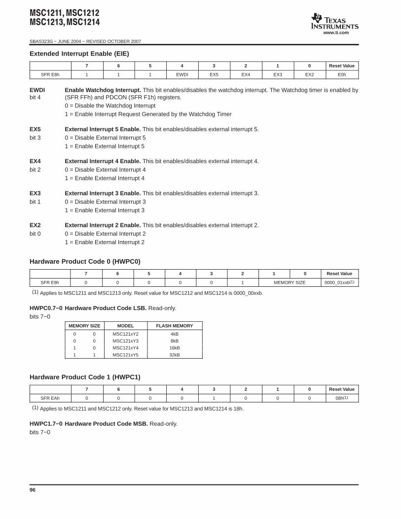
SBAS323G − JUNE 2004 − REVISED OCTOBER 2007
www.ti.com
96
Extended Interrupt Enable (EIE)
7 6 5 4 3 2 1 0 Reset Value
SFR E8h 1 1 1 EWDI EX5 EX4 EX3 EX2 E0h
EWDI Enable Watchdog Interrupt. This bit enables/disables the watchdog interrupt. The Watchdog timer is enabled bybit 4 (SFR FFh) and PDCON (SFR F1h) registers.
0 = Disable the Watchdog Interrupt1 = Enable Interrupt Request Generated by the Watchdog Timer
EX5 External Interrupt 5 Enable. This bit enables/disables external interrupt 5.bit 3 0 = Disable External Interrupt 5
1 = Enable External Interrupt 5
EX4 External Interrupt 4 Enable. This bit enables/disables external interrupt 4.bit 2 0 = Disable External Interrupt 4
1 = Enable External Interrupt 4
EX3 External Interrupt 3 Enable. This bit enables/disables external interrupt 3.bit 1 0 = Disable External Interrupt 3
1 = Enable External Interrupt 3
EX2 External Interrupt 2 Enable. This bit enables/disables external interrupt 2.bit 0 0 = Disable External Interrupt 2
1 = Enable External Interrupt 2
Hardware Product Code 0 (HWPC0)
7 6 5 4 3 2 1 0 Reset Value
SFR E9h 0 0 0 0 0 1 MEMORY SIZE 0000_01xxb(1)
(1) Applies to MSC1211 and MSC1213 only. Reset value for MSC1212 and MSC1214 is 0000_00xxb.
HWPC0.7−0 Hardware Product Code LSB. Read-only.bits 7−0
MEMORY SIZE MODEL FLASH MEMORY
0 0 MSC121xY2 4kB
0 0 MSC121xY3 8kB
1 0 MSC121xY4 16kB
1 1 MSC121xY5 32kB
Hardware Product Code 1 (HWPC1)
7 6 5 4 3 2 1 0 Reset Value
SFR EAh 0 0 0 0 1 0 0 0 08h(1)
(1) Applies to MSC1211 and MSC1212 only. Reset value for MSC1213 and MSC1214 is 18h.
HWPC1.7−0 Hardware Product Code MSB. Read-only.bits 7−0
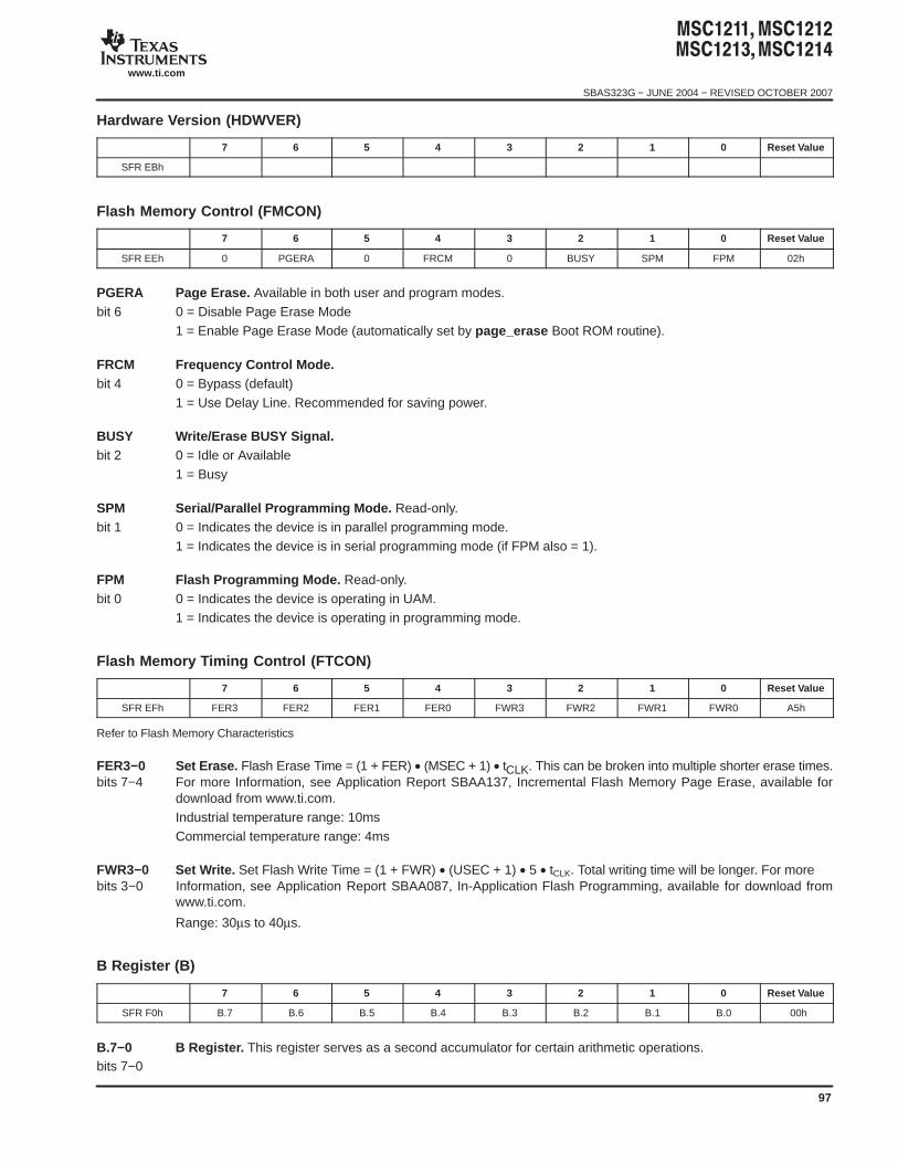
SBAS323G − JUNE 2004 − REVISED OCTOBER 2007
www.ti.com
97
Hardware Version (HDWVER)
7 6 5 4 3 2 1 0 Reset Value
SFR EBh
Flash Memory Control (FMCON)
7 6 5 4 3 2 1 0 Reset Value
SFR EEh 0 PGERA 0 FRCM 0 BUSY SPM FPM 02h
PGERA Page Erase. Available in both user and program modes.bit 6 0 = Disable Page Erase Mode
1 = Enable Page Erase Mode (automatically set by page_erase Boot ROM routine).
FRCM Frequency Control Mode.bit 4 0 = Bypass (default)
1 = Use Delay Line. Recommended for saving power.
BUSY Write/Erase BUSY Signal.bit 2 0 = Idle or Available
1 = Busy
SPM Serial/Parallel Programming Mode. Read-only.bit 1 0 = Indicates the device is in parallel programming mode.
1 = Indicates the device is in serial programming mode (if FPM also = 1).
FPM Flash Programming Mode. Read-only.bit 0 0 = Indicates the device is operating in UAM.
1 = Indicates the device is operating in programming mode.
Flash Memory Timing Control (FTCON)
7 6 5 4 3 2 1 0 Reset Value
SFR EFh FER3 FER2 FER1 FER0 FWR3 FWR2 FWR1 FWR0 A5h
Refer to Flash Memory Characteristics
FER3−0 Set Erase. Flash Erase Time = (1 + FER) • (MSEC + 1) • tCLK. This can be broken into multiple shorter erase times.bits 7−4 For more Information, see Application Report SBAA137, Incremental Flash Memory Page Erase, available for
download from www.ti.com.Industrial temperature range: 10msCommercial temperature range: 4ms
FWR3−0 Set Write. Set Flash Write Time = (1 + FWR) • (USEC + 1) • 5 • tCLK. Total writing time will be longer. For morebits 3−0 Information, see Application Report SBAA087, In-Application Flash Programming, available for download from
www.ti.com.
Range: 30µs to 40µs.
B Register (B)
7 6 5 4 3 2 1 0 Reset Value
SFR F0h B.7 B.6 B.5 B.4 B.3 B.2 B.1 B.0 00h
B.7−0 B Register. This register serves as a second accumulator for certain arithmetic operations.bits 7−0
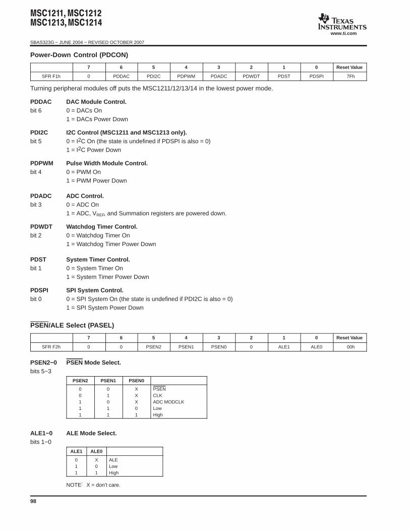
SBAS323G − JUNE 2004 − REVISED OCTOBER 2007
www.ti.com
98
Power-Down Control (PDCON)
7 6 5 4 3 2 1 0 Reset Value
SFR F1h 0 PDDAC PDI2C PDPWM PDADC PDWDT PDST PDSPI 7Fh
Turning peripheral modules off puts the MSC1211/12/13/14 in the lowest power mode.
PDDAC DAC Module Control.bit 6 0 = DACs On
1 = DACs Power Down
PDI2C I2C Control (MSC1211 and MSC1213 only).bit 5 0 = I2C On (the state is undefined if PDSPI is also = 0)
1 = I2C Power Down
PDPWM Pulse Width Module Control.bit 4 0 = PWM On
1 = PWM Power Down
PDADC ADC Control.bit 3 0 = ADC On
1 = ADC, VREF, and Summation registers are powered down.
PDWDT Watchdog Timer Control.bit 2 0 = Watchdog Timer On
1 = Watchdog Timer Power Down
PDST System Timer Control.bit 1 0 = System Timer On
1 = System Timer Power Down
PDSPI SPI System Control.bit 0 0 = SPI System On (the state is undefined if PDI2C is also = 0)
1 = SPI System Power Down
PSEN/ALE Select (PASEL)
7 6 5 4 3 2 1 0 Reset Value
SFR F2h 0 0 PSEN2 PSEN1 PSEN0 0 ALE1 ALE0 00h
PSEN2−0 PSEN Mode Select.bits 5−3
PSEN2 PSEN1 PSEN0
0 0 X PSEN0 1 X CLK1 0 X ADC MODCLK1 1 0 Low1 1 1 High
ALE1−0 ALE Mode Select.bits 1−0
ALE1 ALE0
0 X ALE1 0 Low1 1 High
NOTE: X = don’t care.
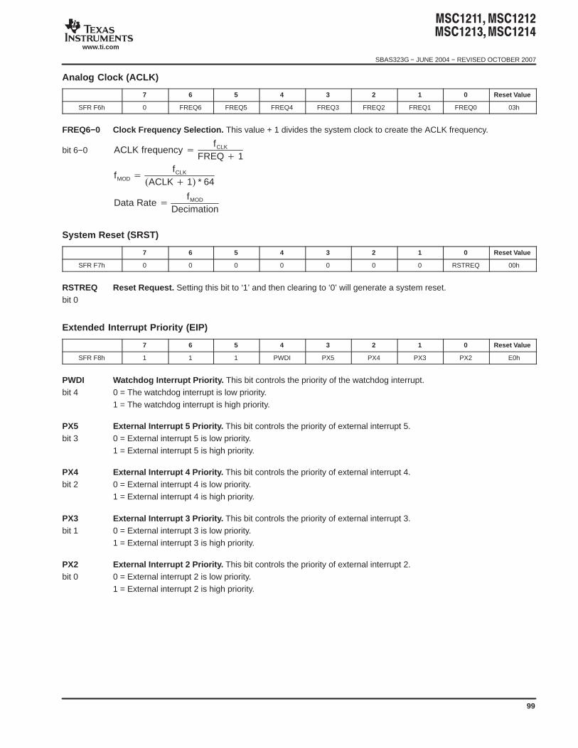
SBAS323G − JUNE 2004 − REVISED OCTOBER 2007
www.ti.com
99
Analog Clock (ACLK)
7 6 5 4 3 2 1 0 Reset Value
SFR F6h 0 FREQ6 FREQ5 FREQ4 FREQ3 FREQ2 FREQ1 FREQ0 03h
FREQ6−0 Clock Frequency Selection. This value + 1 divides the system clock to create the ACLK frequency.
bit 6−0 ACLK frequency fCLK
FREQ 1
fMOD fCLK
ACLK 1 * 64
Data Rate fMOD
Decimation
System Reset (SRST)
7 6 5 4 3 2 1 0 Reset Value
SFR F7h 0 0 0 0 0 0 0 RSTREQ 00h
RSTREQ Reset Request. Setting this bit to ‘1’ and then clearing to ‘0’ will generate a system reset.bit 0
Extended Interrupt Priority (EIP)
7 6 5 4 3 2 1 0 Reset Value
SFR F8h 1 1 1 PWDI PX5 PX4 PX3 PX2 E0h
PWDI Watchdog Interrupt Priority. This bit controls the priority of the watchdog interrupt.bit 4 0 = The watchdog interrupt is low priority.
1 = The watchdog interrupt is high priority.
PX5 External Interrupt 5 Priority. This bit controls the priority of external interrupt 5.bit 3 0 = External interrupt 5 is low priority.
1 = External interrupt 5 is high priority.
PX4 External Interrupt 4 Priority. This bit controls the priority of external interrupt 4.bit 2 0 = External interrupt 4 is low priority.
1 = External interrupt 4 is high priority.
PX3 External Interrupt 3 Priority. This bit controls the priority of external interrupt 3.bit 1 0 = External interrupt 3 is low priority.
1 = External interrupt 3 is high priority.
PX2 External Interrupt 2 Priority. This bit controls the priority of external interrupt 2.bit 0 0 = External interrupt 2 is low priority.
1 = External interrupt 2 is high priority.
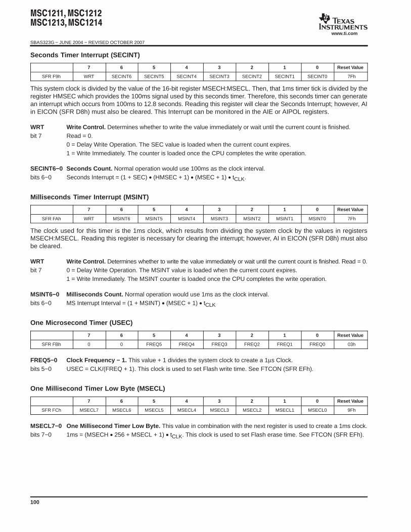
SBAS323G − JUNE 2004 − REVISED OCTOBER 2007
www.ti.com
100
Seconds Timer Interrupt (SECINT)
7 6 5 4 3 2 1 0 Reset Value
SFR F9h WRT SECINT6 SECINT5 SECINT4 SECINT3 SECINT2 SECINT1 SECINT0 7Fh
This system clock is divided by the value of the 16-bit register MSECH:MSECL. Then, that 1ms timer tick is divided by theregister HMSEC which provides the 100ms signal used by this seconds timer. Therefore, this seconds timer can generatean interrupt which occurs from 100ms to 12.8 seconds. Reading this register will clear the Seconds Interrupt; however, AIin EICON (SFR D8h) must also be cleared. This Interrupt can be monitored in the AIE or AIPOL registers.
WRT Write Control. Determines whether to write the value immediately or wait until the current count is finished.bit 7 Read = 0.
0 = Delay Write Operation. The SEC value is loaded when the current count expires.1 = Write Immediately. The counter is loaded once the CPU completes the write operation.
SECINT6−0 Seconds Count. Normal operation would use 100ms as the clock interval.bits 6−0 Seconds Interrupt = (1 + SEC) • (HMSEC + 1) • (MSEC + 1) • tCLK.
Milliseconds Timer Interrupt (MSINT)
7 6 5 4 3 2 1 0 Reset Value
SFR FAh WRT MSINT6 MSINT5 MSINT4 MSINT3 MSINT2 MSINT1 MSINT0 7Fh
The clock used for this timer is the 1ms clock, which results from dividing the system clock by the values in registersMSECH:MSECL. Reading this register is necessary for clearing the interrupt; however, AI in EICON (SFR D8h) must alsobe cleared.
WRT Write Control. Determines whether to write the value immediately or wait until the current count is finished. Read = 0.bit 7 0 = Delay Write Operation. The MSINT value is loaded when the current count expires.
1 = Write Immediately. The MSINT counter is loaded once the CPU completes the write operation.
MSINT6−0 Milliseconds Count. Normal operation would use 1ms as the clock interval.bits 6−0 MS Interrupt Interval = (1 + MSINT) • (MSEC + 1) • tCLK
One Microsecond Timer (USEC)
7 6 5 4 3 2 1 0 Reset Value
SFR FBh 0 0 FREQ5 FREQ4 FREQ3 FREQ2 FREQ1 FREQ0 03h
FREQ5−0 Clock Frequency − 1. This value + 1 divides the system clock to create a 1µs Clock.bits 5−0 USEC = CLK/(FREQ + 1). This clock is used to set Flash write time. See FTCON (SFR EFh).
One Millisecond Timer Low Byte (MSECL)
7 6 5 4 3 2 1 0 Reset Value
SFR FCh MSECL7 MSECL6 MSECL5 MSECL4 MSECL3 MSECL2 MSECL1 MSECL0 9Fh
MSECL7−0 One Millisecond Timer Low Byte. This value in combination with the next register is used to create a 1ms clock.bits 7−0 1ms = (MSECH • 256 + MSECL + 1) • tCLK. This clock is used to set Flash erase time. See FTCON (SFR EFh).
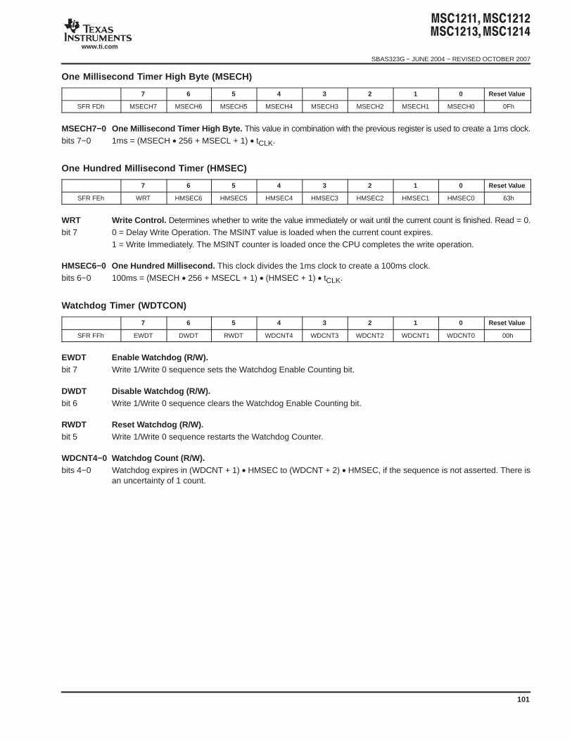
SBAS323G − JUNE 2004 − REVISED OCTOBER 2007
www.ti.com
101
One Millisecond Timer High Byte (MSECH)
7 6 5 4 3 2 1 0 Reset Value
SFR FDh MSECH7 MSECH6 MSECH5 MSECH4 MSECH3 MSECH2 MSECH1 MSECH0 0Fh
MSECH7−0 One Millisecond T imer High Byte. This value in combination with the previous register is used to create a 1ms clock.bits 7−0 1ms = (MSECH • 256 + MSECL + 1) • tCLK.
One Hundred Millisecond Timer (HMSEC)
7 6 5 4 3 2 1 0 Reset Value
SFR FEh WRT HMSEC6 HMSEC5 HMSEC4 HMSEC3 HMSEC2 HMSEC1 HMSEC0 63h
WRT Write Control. Determines whether to write the value immediately or wait until the current count is finished. Read = 0.bit 7 0 = Delay Write Operation. The MSINT value is loaded when the current count expires.
1 = Write Immediately. The MSINT counter is loaded once the CPU completes the write operation.
HMSEC6−0 One Hundred Millisecond. This clock divides the 1ms clock to create a 100ms clock.bits 6−0 100ms = (MSECH • 256 + MSECL + 1) • (HMSEC + 1) • tCLK.
Watchdog Timer (WDTCON)
7 6 5 4 3 2 1 0 Reset Value
SFR FFh EWDT DWDT RWDT WDCNT4 WDCNT3 WDCNT2 WDCNT1 WDCNT0 00h
EWDT Enable Watchdog (R/W).bit 7 Write 1/Write 0 sequence sets the Watchdog Enable Counting bit.
DWDT Disable Watchdog (R/W).bit 6 Write 1/Write 0 sequence clears the Watchdog Enable Counting bit.
RWDT Reset Watchdog (R/W).bit 5 Write 1/Write 0 sequence restarts the Watchdog Counter.
WDCNT4−0 Watchdog Count (R/W).bits 4−0 Watchdog expires in (WDCNT + 1) • HMSEC to (WDCNT + 2) • HMSEC, if the sequence is not asserted. There is
an uncertainty of 1 count.

SBAS323G − JUNE 2004 − REVISED OCTOBER 2007
www.ti.com
102
Revision History
DATE REV PAGE SECTION DESCRIPTION
10/07 G 29 Voltage Reference Added paragraph to end of section.
7/06 F 32 Brownout Reset Added paragraph on BOR voltage calibration.
NOTE: Page numbers for previous revisions may differ from page numbers in the current version.
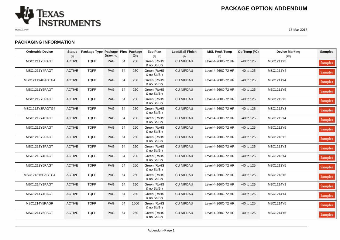
PACKAGE OPTION ADDENDUM
www.ti.com 17-Mar-2017
Addendum-Page 1
PACKAGING INFORMATION
Orderable Device Status(1)
Package Type PackageDrawing
Pins PackageQty
Eco Plan(2)
Lead/Ball Finish(6)
MSL Peak Temp(3)
Op Temp (°C) Device Marking(4/5)
Samples
MSC1211Y3PAGT ACTIVE TQFP PAG 64 250 Green (RoHS& no Sb/Br)
CU NIPDAU Level-4-260C-72 HR -40 to 125 MSC1211Y3
MSC1211Y4PAGT ACTIVE TQFP PAG 64 250 Green (RoHS& no Sb/Br)
CU NIPDAU Level-4-260C-72 HR -40 to 125 MSC1211Y4
MSC1211Y4PAGTG4 ACTIVE TQFP PAG 64 250 Green (RoHS& no Sb/Br)
CU NIPDAU Level-4-260C-72 HR -40 to 125 MSC1211Y4
MSC1211Y5PAGT ACTIVE TQFP PAG 64 250 Green (RoHS& no Sb/Br)
CU NIPDAU Level-4-260C-72 HR -40 to 125 MSC1211Y5
MSC1212Y3PAGT ACTIVE TQFP PAG 64 250 Green (RoHS& no Sb/Br)
CU NIPDAU Level-4-260C-72 HR -40 to 125 MSC1212Y3
MSC1212Y3PAGTG4 ACTIVE TQFP PAG 64 250 Green (RoHS& no Sb/Br)
CU NIPDAU Level-4-260C-72 HR -40 to 125 MSC1212Y3
MSC1212Y4PAGT ACTIVE TQFP PAG 64 250 Green (RoHS& no Sb/Br)
CU NIPDAU Level-4-260C-72 HR -40 to 125 MSC1212Y4
MSC1212Y5PAGT ACTIVE TQFP PAG 64 250 Green (RoHS& no Sb/Br)
CU NIPDAU Level-4-260C-72 HR -40 to 125 MSC1212Y5
MSC1213Y2PAGT ACTIVE TQFP PAG 64 250 Green (RoHS& no Sb/Br)
CU NIPDAU Level-4-260C-72 HR -40 to 125 MSC1213Y2
MSC1213Y3PAGT ACTIVE TQFP PAG 64 250 Green (RoHS& no Sb/Br)
CU NIPDAU Level-4-260C-72 HR -40 to 125 MSC1213Y3
MSC1213Y4PAGT ACTIVE TQFP PAG 64 250 Green (RoHS& no Sb/Br)
CU NIPDAU Level-4-260C-72 HR -40 to 125 MSC1213Y4
MSC1213Y5PAGT ACTIVE TQFP PAG 64 250 Green (RoHS& no Sb/Br)
CU NIPDAU Level-4-260C-72 HR -40 to 125 MSC1213Y5
MSC1213Y5PAGTG4 ACTIVE TQFP PAG 64 250 Green (RoHS& no Sb/Br)
CU NIPDAU Level-4-260C-72 HR -40 to 125 MSC1213Y5
MSC1214Y3PAGT ACTIVE TQFP PAG 64 250 Green (RoHS& no Sb/Br)
CU NIPDAU Level-4-260C-72 HR -40 to 125 MSC1214Y3
MSC1214Y4PAGT ACTIVE TQFP PAG 64 250 Green (RoHS& no Sb/Br)
CU NIPDAU Level-4-260C-72 HR -40 to 125 MSC1214Y4
MSC1214Y5PAGR ACTIVE TQFP PAG 64 1500 Green (RoHS& no Sb/Br)
CU NIPDAU Level-4-260C-72 HR -40 to 125 MSC1214Y5
MSC1214Y5PAGT ACTIVE TQFP PAG 64 250 Green (RoHS& no Sb/Br)
CU NIPDAU Level-4-260C-72 HR -40 to 125 MSC1214Y5

PACKAGE OPTION ADDENDUM
www.ti.com 17-Mar-2017
Addendum-Page 2
(1) The marketing status values are defined as follows:ACTIVE: Product device recommended for new designs.LIFEBUY: TI has announced that the device will be discontinued, and a lifetime-buy period is in effect.NRND: Not recommended for new designs. Device is in production to support existing customers, but TI does not recommend using this part in a new design.PREVIEW: Device has been announced but is not in production. Samples may or may not be available.OBSOLETE: TI has discontinued the production of the device.
(2) Eco Plan - The planned eco-friendly classification: Pb-Free (RoHS), Pb-Free (RoHS Exempt), or Green (RoHS & no Sb/Br) - please check http://www.ti.com/productcontent for the latest availabilityinformation and additional product content details.TBD: The Pb-Free/Green conversion plan has not been defined.Pb-Free (RoHS): TI's terms "Lead-Free" or "Pb-Free" mean semiconductor products that are compatible with the current RoHS requirements for all 6 substances, including the requirement thatlead not exceed 0.1% by weight in homogeneous materials. Where designed to be soldered at high temperatures, TI Pb-Free products are suitable for use in specified lead-free processes.Pb-Free (RoHS Exempt): This component has a RoHS exemption for either 1) lead-based flip-chip solder bumps used between the die and package, or 2) lead-based die adhesive used betweenthe die and leadframe. The component is otherwise considered Pb-Free (RoHS compatible) as defined above.Green (RoHS & no Sb/Br): TI defines "Green" to mean Pb-Free (RoHS compatible), and free of Bromine (Br) and Antimony (Sb) based flame retardants (Br or Sb do not exceed 0.1% by weightin homogeneous material)
(3) MSL, Peak Temp. - The Moisture Sensitivity Level rating according to the JEDEC industry standard classifications, and peak solder temperature.
(4) There may be additional marking, which relates to the logo, the lot trace code information, or the environmental category on the device.
(5) Multiple Device Markings will be inside parentheses. Only one Device Marking contained in parentheses and separated by a "~" will appear on a device. If a line is indented then it is a continuationof the previous line and the two combined represent the entire Device Marking for that device.
(6) Lead/Ball Finish - Orderable Devices may have multiple material finish options. Finish options are separated by a vertical ruled line. Lead/Ball Finish values may wrap to two lines if the finishvalue exceeds the maximum column width.
Important Information and Disclaimer:The information provided on this page represents TI's knowledge and belief as of the date that it is provided. TI bases its knowledge and belief on informationprovided by third parties, and makes no representation or warranty as to the accuracy of such information. Efforts are underway to better integrate information from third parties. TI has taken andcontinues to take reasonable steps to provide representative and accurate information but may not have conducted destructive testing or chemical analysis on incoming materials and chemicals.TI and TI suppliers consider certain information to be proprietary, and thus CAS numbers and other limited information may not be available for release.
In no event shall TI's liability arising out of such information exceed the total purchase price of the TI part(s) at issue in this document sold by TI to Customer on an annual basis.
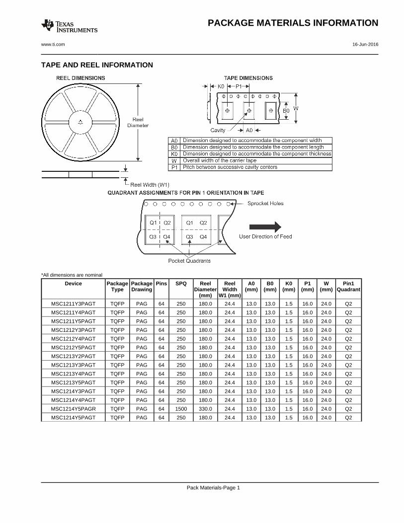
TAPE AND REEL INFORMATION
*All dimensions are nominal
Device PackageType
PackageDrawing
Pins SPQ ReelDiameter
(mm)
ReelWidth
W1 (mm)
A0(mm)
B0(mm)
K0(mm)
P1(mm)
W(mm)
Pin1Quadrant
MSC1211Y3PAGT TQFP PAG 64 250 180.0 24.4 13.0 13.0 1.5 16.0 24.0 Q2
MSC1211Y4PAGT TQFP PAG 64 250 180.0 24.4 13.0 13.0 1.5 16.0 24.0 Q2
MSC1211Y5PAGT TQFP PAG 64 250 180.0 24.4 13.0 13.0 1.5 16.0 24.0 Q2
MSC1212Y3PAGT TQFP PAG 64 250 180.0 24.4 13.0 13.0 1.5 16.0 24.0 Q2
MSC1212Y4PAGT TQFP PAG 64 250 180.0 24.4 13.0 13.0 1.5 16.0 24.0 Q2
MSC1212Y5PAGT TQFP PAG 64 250 180.0 24.4 13.0 13.0 1.5 16.0 24.0 Q2
MSC1213Y2PAGT TQFP PAG 64 250 180.0 24.4 13.0 13.0 1.5 16.0 24.0 Q2
MSC1213Y3PAGT TQFP PAG 64 250 180.0 24.4 13.0 13.0 1.5 16.0 24.0 Q2
MSC1213Y4PAGT TQFP PAG 64 250 180.0 24.4 13.0 13.0 1.5 16.0 24.0 Q2
MSC1213Y5PAGT TQFP PAG 64 250 180.0 24.4 13.0 13.0 1.5 16.0 24.0 Q2
MSC1214Y3PAGT TQFP PAG 64 250 180.0 24.4 13.0 13.0 1.5 16.0 24.0 Q2
MSC1214Y4PAGT TQFP PAG 64 250 180.0 24.4 13.0 13.0 1.5 16.0 24.0 Q2
MSC1214Y5PAGR TQFP PAG 64 1500 330.0 24.4 13.0 13.0 1.5 16.0 24.0 Q2
MSC1214Y5PAGT TQFP PAG 64 250 180.0 24.4 13.0 13.0 1.5 16.0 24.0 Q2
PACKAGE MATERIALS INFORMATION
www.ti.com 16-Jun-2016
Pack Materials-Page 1
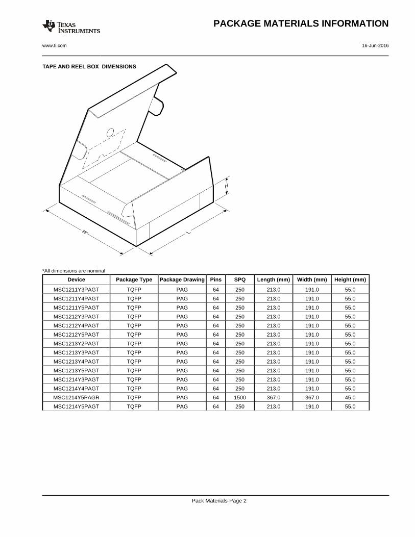
*All dimensions are nominal
Device Package Type Package Drawing Pins SPQ Length (mm) Width (mm) Height (mm)
MSC1211Y3PAGT TQFP PAG 64 250 213.0 191.0 55.0
MSC1211Y4PAGT TQFP PAG 64 250 213.0 191.0 55.0
MSC1211Y5PAGT TQFP PAG 64 250 213.0 191.0 55.0
MSC1212Y3PAGT TQFP PAG 64 250 213.0 191.0 55.0
MSC1212Y4PAGT TQFP PAG 64 250 213.0 191.0 55.0
MSC1212Y5PAGT TQFP PAG 64 250 213.0 191.0 55.0
MSC1213Y2PAGT TQFP PAG 64 250 213.0 191.0 55.0
MSC1213Y3PAGT TQFP PAG 64 250 213.0 191.0 55.0
MSC1213Y4PAGT TQFP PAG 64 250 213.0 191.0 55.0
MSC1213Y5PAGT TQFP PAG 64 250 213.0 191.0 55.0
MSC1214Y3PAGT TQFP PAG 64 250 213.0 191.0 55.0
MSC1214Y4PAGT TQFP PAG 64 250 213.0 191.0 55.0
MSC1214Y5PAGR TQFP PAG 64 1500 367.0 367.0 45.0
MSC1214Y5PAGT TQFP PAG 64 250 213.0 191.0 55.0
PACKAGE MATERIALS INFORMATION
www.ti.com 16-Jun-2016
Pack Materials-Page 2
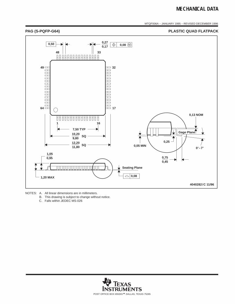
MECHANICAL DATA
MTQF006A – JANUARY 1995 – REVISED DECEMBER 1996
POST OFFICE BOX 655303 • DALLAS, TEXAS 75265
PAG (S-PQFP-G64) PLASTIC QUAD FLATPACK
0,13 NOM
0,25
0,450,75
Seating Plane
0,05 MIN
4040282/C 11/96
Gage Plane
33
0,170,27
16
48
1
7,50 TYP
49
64
SQ
9,80
1,050,95
11,8012,20
1,20 MAX
10,20SQ
17
32
0,08
0,50 M0,08
0°–7°
NOTES: A. All linear dimensions are in millimeters.B. This drawing is subject to change without notice.C. Falls within JEDEC MS-026

IMPORTANT NOTICE
Texas Instruments Incorporated (TI) reserves the right to make corrections, enhancements, improvements and other changes to itssemiconductor products and services per JESD46, latest issue, and to discontinue any product or service per JESD48, latest issue. Buyersshould obtain the latest relevant information before placing orders and should verify that such information is current and complete.TI’s published terms of sale for semiconductor products (http://www.ti.com/sc/docs/stdterms.htm) apply to the sale of packaged integratedcircuit products that TI has qualified and released to market. Additional terms may apply to the use or sale of other types of TI products andservices.Reproduction of significant portions of TI information in TI data sheets is permissible only if reproduction is without alteration and isaccompanied by all associated warranties, conditions, limitations, and notices. TI is not responsible or liable for such reproduceddocumentation. Information of third parties may be subject to additional restrictions. Resale of TI products or services with statementsdifferent from or beyond the parameters stated by TI for that product or service voids all express and any implied warranties for theassociated TI product or service and is an unfair and deceptive business practice. TI is not responsible or liable for any such statements.Buyers and others who are developing systems that incorporate TI products (collectively, “Designers”) understand and agree that Designersremain responsible for using their independent analysis, evaluation and judgment in designing their applications and that Designers havefull and exclusive responsibility to assure the safety of Designers' applications and compliance of their applications (and of all TI productsused in or for Designers’ applications) with all applicable regulations, laws and other applicable requirements. Designer represents that, withrespect to their applications, Designer has all the necessary expertise to create and implement safeguards that (1) anticipate dangerousconsequences of failures, (2) monitor failures and their consequences, and (3) lessen the likelihood of failures that might cause harm andtake appropriate actions. Designer agrees that prior to using or distributing any applications that include TI products, Designer willthoroughly test such applications and the functionality of such TI products as used in such applications.TI’s provision of technical, application or other design advice, quality characterization, reliability data or other services or information,including, but not limited to, reference designs and materials relating to evaluation modules, (collectively, “TI Resources”) are intended toassist designers who are developing applications that incorporate TI products; by downloading, accessing or using TI Resources in anyway, Designer (individually or, if Designer is acting on behalf of a company, Designer’s company) agrees to use any particular TI Resourcesolely for this purpose and subject to the terms of this Notice.TI’s provision of TI Resources does not expand or otherwise alter TI’s applicable published warranties or warranty disclaimers for TIproducts, and no additional obligations or liabilities arise from TI providing such TI Resources. TI reserves the right to make corrections,enhancements, improvements and other changes to its TI Resources. TI has not conducted any testing other than that specificallydescribed in the published documentation for a particular TI Resource.Designer is authorized to use, copy and modify any individual TI Resource only in connection with the development of applications thatinclude the TI product(s) identified in such TI Resource. NO OTHER LICENSE, EXPRESS OR IMPLIED, BY ESTOPPEL OR OTHERWISETO ANY OTHER TI INTELLECTUAL PROPERTY RIGHT, AND NO LICENSE TO ANY TECHNOLOGY OR INTELLECTUAL PROPERTYRIGHT OF TI OR ANY THIRD PARTY IS GRANTED HEREIN, including but not limited to any patent right, copyright, mask work right, orother intellectual property right relating to any combination, machine, or process in which TI products or services are used. Informationregarding or referencing third-party products or services does not constitute a license to use such products or services, or a warranty orendorsement thereof. Use of TI Resources may require a license from a third party under the patents or other intellectual property of thethird party, or a license from TI under the patents or other intellectual property of TI.TI RESOURCES ARE PROVIDED “AS IS” AND WITH ALL FAULTS. TI DISCLAIMS ALL OTHER WARRANTIES ORREPRESENTATIONS, EXPRESS OR IMPLIED, REGARDING RESOURCES OR USE THEREOF, INCLUDING BUT NOT LIMITED TOACCURACY OR COMPLETENESS, TITLE, ANY EPIDEMIC FAILURE WARRANTY AND ANY IMPLIED WARRANTIES OFMERCHANTABILITY, FITNESS FOR A PARTICULAR PURPOSE, AND NON-INFRINGEMENT OF ANY THIRD PARTY INTELLECTUALPROPERTY RIGHTS. TI SHALL NOT BE LIABLE FOR AND SHALL NOT DEFEND OR INDEMNIFY DESIGNER AGAINST ANY CLAIM,INCLUDING BUT NOT LIMITED TO ANY INFRINGEMENT CLAIM THAT RELATES TO OR IS BASED ON ANY COMBINATION OFPRODUCTS EVEN IF DESCRIBED IN TI RESOURCES OR OTHERWISE. IN NO EVENT SHALL TI BE LIABLE FOR ANY ACTUAL,DIRECT, SPECIAL, COLLATERAL, INDIRECT, PUNITIVE, INCIDENTAL, CONSEQUENTIAL OR EXEMPLARY DAMAGES INCONNECTION WITH OR ARISING OUT OF TI RESOURCES OR USE THEREOF, AND REGARDLESS OF WHETHER TI HAS BEENADVISED OF THE POSSIBILITY OF SUCH DAMAGES.Unless TI has explicitly designated an individual product as meeting the requirements of a particular industry standard (e.g., ISO/TS 16949and ISO 26262), TI is not responsible for any failure to meet such industry standard requirements.Where TI specifically promotes products as facilitating functional safety or as compliant with industry functional safety standards, suchproducts are intended to help enable customers to design and create their own applications that meet applicable functional safety standardsand requirements. Using products in an application does not by itself establish any safety features in the application. Designers mustensure compliance with safety-related requirements and standards applicable to their applications. Designer may not use any TI products inlife-critical medical equipment unless authorized officers of the parties have executed a special contract specifically governing such use.Life-critical medical equipment is medical equipment where failure of such equipment would cause serious bodily injury or death (e.g., lifesupport, pacemakers, defibrillators, heart pumps, neurostimulators, and implantables). Such equipment includes, without limitation, allmedical devices identified by the U.S. Food and Drug Administration as Class III devices and equivalent classifications outside the U.S.TI may expressly designate certain products as completing a particular qualification (e.g., Q100, Military Grade, or Enhanced Product).Designers agree that it has the necessary expertise to select the product with the appropriate qualification designation for their applicationsand that proper product selection is at Designers’ own risk. Designers are solely responsible for compliance with all legal and regulatoryrequirements in connection with such selection.Designer will fully indemnify TI and its representatives against any damages, costs, losses, and/or liabilities arising out of Designer’s non-compliance with the terms and provisions of this Notice.
Mailing Address: Texas Instruments, Post Office Box 655303, Dallas, Texas 75265Copyright © 2018, Texas Instruments Incorporated