Embed Size (px)
Citation preview
306 Principles of Electronics
12.1 Transistor Audio Power Amplifier 12.2 Small-Signal and Large-Signal
Amplifiers 12.3 Output Power of Amplifier 12.4 Difference Between Voltage and
Power Amplifiers 12.5 Performance Quantities of Power
Amplifiers 12.6 Classification of Power Amplifiers 12.7 Expression for Collector Efficiency 12.8 Maximum Collector
Efficiency of Series – Fed Class AAmplifier
12.9 Maximum CollectorEfficiency of Transformer CoupledClass A Power Amplifier
12.10 Important Points About Class APower Amplifier
12.11 Thermal Runaway12.12 Heat Sink12.13 Mathematical Analysis12.14 Stages Of A Practical Power
Amplifier12.15 Driver Stage12.16 Output Stage12.17 Push-Pull Amplifier12.18 Maximum Efficiency for Class B
Power Amplifier
12.19 Complementary-SymmetryAmplifier
INTRINTRINTRINTRINTRODUCTIONODUCTIONODUCTIONODUCTIONODUCTION
A practical amplifier always consists of a num-ber of stages that amplify a weak signal untilsufficient power is available to operate a loud-
speaker or other output device. The first few stages inthis multistage amplifier have the function of only volt-age amplification. However, the last stage is designedto provide maximum power. This final stage is knownas power stage.
The term audio means the range of frequencieswhich our ears can hear. The range of human hearingextends from 20 Hz to 20 kHz. Therefore, audio am-plifiers amplify electrical signals that have a frequencyrange corresponding to the range of human hearing i.e.20 Hz to 20 kHz. Fig. 12.1 shows the block diagram ofan audio amplifier. The early stages build up the volt-age level of the signal while the last stage builds uppower to a level sufficient to operate the loudspeaker.In this chapter, we shall talk about the final stage in amultistage amplifier—the power amplifier.
Transistor AudioPower Amplifiers
12
Transistor Audio Power Amplifiers 307
Fig. 12.1
12.1 Transistor Audio Power AmplifierA transistor amplifier which raises the power level of thesignals that have audio frequency range is known as tran-sistor audio power amplifier.
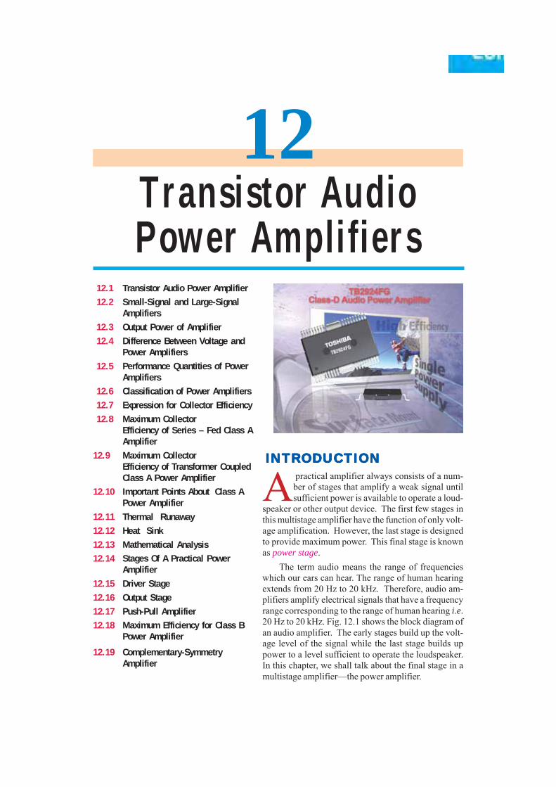
In general, the last stage of a multistage amplifier is thepower stage. The power amplifier differs from all theprevious stages in that here a concentrated effort is made toobtain maximum output power. A transistor that is suitablefor power amplification is generally called a powertransistor. It differs from other transistors mostly in size ; itis considerably larger to provide for handling the greatamount of power. Audio power amplifiers are used to delivera large amount of power to a low resistance load. Typicalload values range from 300Ω (for transmission antennas) to8Ω (for loudspeakers). Although these load values do notcover every possibility, they do illustrate the fact that audiopower amplifiers usually drive low-resistance loads. Thetypical power output rating of a power amplifier is 1W ormore.
12.2 Small-Signal and Large-Signal AmplifiersThe input signal to a multistage amplifier is generally small (a few mV from a cassette or CD or a few μVfrom an antenna). Therefore, the first few stages of a multistage amplifier handle small signals andhave the function of only voltage amplification. However, the last stage handles a large signal and itsjob is to produce a large amount of power in order to operate the output device (e.g. speaker).
(i) Small-signal amplifiers. Those amplifiers which handle small input a.c. signals (a few μVor a few mV) are called small-signal amplifiers. Voltage amplifiers generally fall in this class. Thesmall-signal amplifiers are designed to operate over the linear portion of the output characteristics.Therefore, the transistor parameters such as current gain, input impedance, output impedance etc. donot change as the amplitude of the signal changes. Such amplifiers amplify the signal with little or nodistortion.
(ii) Large-signal amplifiers. Those amplifiers which handle large input a.c. signals (a fewvolts) are called large-signal amplifiers. Power amplifiers fall in this class. The large-signal amplifi-ers are designed to provide a large amount of a.c. power output so that they can operate the outputdevice e.g. a speaker. The main features of a large-signal amplifier or power amplifier are the circuit’spower efficiency, the maximum amount of power that the circuit is capable of handling and the im-pedance matching to the output device. It may be noted that all large-signal amplifiers are not neces-
Transistor Audio Power Amplifiers
308 Principles of Electronics
sarily power amplifiers but it is safe to say that most are. In general, where amount of power involvedis 1W or more, the amplifier is termed as power amplifier.
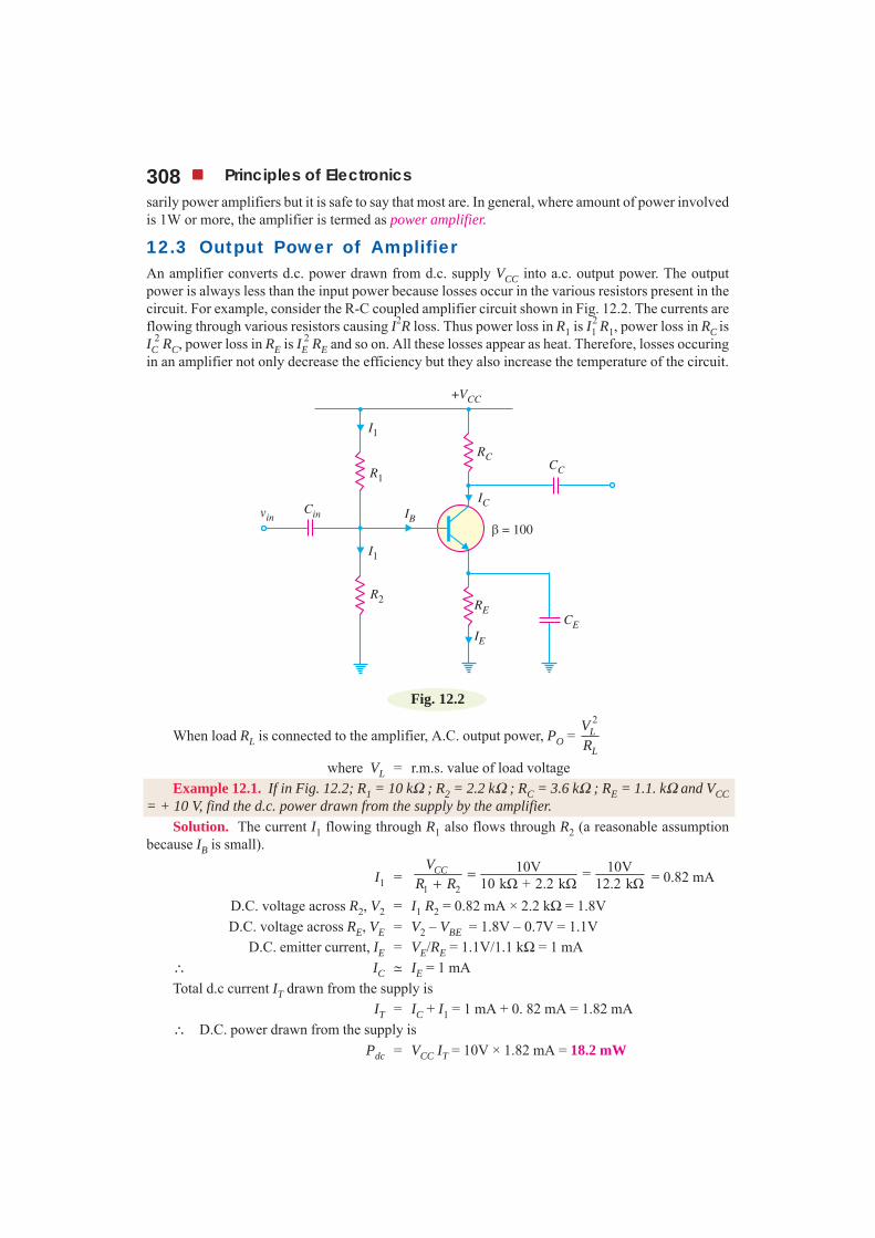
12.3 Output Power of AmplifierAn amplifier converts d.c. power drawn from d.c. supply VCC into a.c. output power. The outputpower is always less than the input power because losses occur in the various resistors present in thecircuit. For example, consider the R-C coupled amplifier circuit shown in Fig. 12.2. The currents areflowing through various resistors causing I2R loss. Thus power loss in R1 is I1
2 R1, power loss in RC isIC
2 RC, power loss in RE is IE2 RE and so on. All these losses appear as heat. Therefore, losses occuring
in an amplifier not only decrease the efficiency but they also increase the temperature of the circuit.
Fig. 12.2
When load RL is connected to the amplifier, A.C. output power, PO = 2
L
L
VR
where VL = r.m.s. value of load voltageExample 12.1. If in Fig. 12.2; R1 = 10 kΩ ; R2 = 2.2 kΩ ; RC = 3.6 kΩ ; RE = 1.1. kΩ and VCC
= + 10 V, find the d.c. power drawn from the supply by the amplifier.Solution. The current I1 flowing through R1 also flows through R2 (a reasonable assumption
because IB is small).
I1 =1 2
10V 10V=10 kΩ + 2.2 kΩ 12.2 kΩ
CCVR R
=+ = 0.82 mA
D.C. voltage across R2, V2 = I1 R2 = 0.82 mA × 2.2 kΩ = 1.8VD.C. voltage across RE, VE = V2 – VBE = 1.8V – 0.7V = 1.1V
D.C. emitter current, IE = VE/RE = 1.1V/1.1 kΩ = 1 mA∴ IC j IE = 1 mATotal d.c current IT drawn from the supply is
IT = IC + I1 = 1 mA + 0. 82 mA = 1.82 mA∴ D.C. power drawn from the supply is
Pdc = VCC IT = 10V × 1.82 mA = 18.2 mW
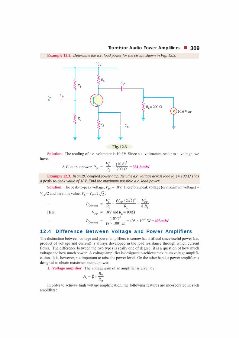
Transistor Audio Power Amplifiers 309Example 12.2. Determine the a.c. load power for the circuit shown in Fig. 12.3.
Fig. 12.3
Solution. The reading of a.c. voltmeter is 10.6V. Since a.c. voltmeters read r.m.s. voltage, wehave,
A.C. output power, PO =2 2(10.6)
200 ΩL
L
VR
= = 561.8 mW
Example 12.3. In an RC coupled power amplifier, the a.c. voltage across load RL (= 100 Ω ) hasa peak- to-peak value of 18V. Find the maximum possible a.c. load power.
Solution. The peak-to-peak voltage, VPP = 18V. Therefore, peak voltage (or maximum voltage) =VPP/2 and the r.m.s value, VL = VPP/2 2 .
∴ PO (max) =2 2 2( / 2 2)
8L PP PP
L L L
V V VR R R
= =
Here VPP = 18V and RL = 100Ω
∴ PO (max) =2(18 )
(8 × 100) ΩV = 405 × 10–3 W = 405 mW
12.4 Difference Between Voltage and Power AmplifiersThe distinction between voltage and power amplifiers is somewhat artificial since useful power (i.e.product of voltage and current) is always developed in the load resistance through which currentflows. The difference between the two types is really one of degree; it is a question of how muchvoltage and how much power. A voltage amplifier is designed to achieve maximum voltage amplifi-cation. It is, however, not important to raise the power level. On the other hand, a power amplifier isdesigned to obtain maximum output power.
1. Voltage amplifier. The voltage gain of an amplifier is given by :
Av = β × C
in
RR
In order to achieve high voltage amplification, the following features are incorporated in suchamplifiers :
310 Principles of Electronics
(i) The transistor with high β ( >100) is used in the circuit. In other words, those transistors areemployed which have thin base.
(ii) The input resistance Rin of the transistor is sought to be quite low as compared to thecollector load RC.
(iii) A relatively high load RC is used in the collector. To permit this condition, voltage amplifiersare always operated at low collector currents (j 1 mA). If the collector current is small, we can uselarge RC in the collector circuit.
2. Power amplifier. A power amplifier is required to deliver a large amount of power and as suchit has to handle large current. In order to achieve high power amplification, the following features areincorporated in such amplifiers :
(i) The size of power transistor is made considerably larger in order to dissipate the heat pro-duced in the transistor during operation.
(ii) The base is made thicker to handle large currents. In other words, transistors with compara-tively smaller β are used.
(iii) Transformer coupling is used for impedance matching.The comparison between voltage and power amplifiers is given below in the tabular form :
S. No. Particular Voltage amplifier Power amplifier1. β High (> 100) low (5 to 20)2. RC High (4 – 10 kΩ) low (5 to 20 Ω)3. Coupling usually R − C coupling Invariably transformer coupling4. Input voltage low (a few mV) High ( 2 − 4 V)5. Collector current low (j 1 mA) High ( > 100 mA)6. Power output low high7. Output impedance High (j 12 kΩ) low (200 Ω)
Example 12.4. A power amplifier operated from 12V battery gives an output of 2W. Find themaximum collector current in the circuit.
Solution.Let IC be the maximum collector current.
Power = battery voltage × collector currentor 2 = 12 × IC
∴ IC = 2 112 6
= A = 166.7 mA
This example shows that a power amplifier handles large power as well as large current.Example 12.5. A voltage amplifier operated from a 12 V battery has a collector load of 4 kΩ.
Find the maximum collector current in the circuit.Solution.The maximum collector current will flow when the whole battery voltage is dropped across RC.
∴ Max. collector current = battery voltagecollector load
= 12 V4 kΩ = 3 mA
This example shows that a voltage amplifier handles small current.Example 12.6. A power amplifier supplies 50 W to an 8-ohm speaker. Find (i) a.c. output
voltage (ii) a.c. output current.
Transistor Audio Power Amplifiers 311Solution.(i) P = V 2/R
∴ a.c. output voltage, V = 50 8PR = × = 20 V
(ii) a.c. output current, I = V/R = 20/8 = 2.5 A
12.5 Performance Quantities of Power AmplifiersAs mentioned previously, the prime objective for a power amplifier is to obtain maximum outputpower. Since a transistor, like any other electronic device has voltage, current and power dissipationlimits, therefore, the criteria for a power amplifier are : collector efficiency, distortion and powerdissipation capability.
(i) Collector efficiency. The main criterion for a power amplifier is not the power gain ratherit is the maximum a.c. power output. Now, an amplifier converts d.c. power from supplyinto a.c. power output. Therefore, the ability of a power amplifier to convert d.c. powerfrom supply into a.c. output power is a measure of its effectiveness. This is known ascollector efficiency and may be defined as under :
The ratio of a.c. output power to the zero signal power (i.e. d.c. power) supplied by the batteryof a power amplifier is known as collector efficiency.
Collector efficiency means as to how well an amplifier converts d.c. power from the battery intoa.c. output power. For instance, if the d.c. power supplied by the battery is 10W and a.c. output poweris 2W, then collector efficiency is 20%. The greater the collector efficiency, the larger is the a.c.power output. It is obvious that for power amplifiers, maximum collector efficiency is the desiredgoal.
(ii) Distortion. The change of output waveshape from the input wave shape of anamplifier is known as distortion.
A transistor like other electronic devices, isessentially a non-linear device. Therefore, when-ever a signal is applied to the input of the transis-tor, the output signal is not exactly like the inputsignal i.e. distortion occurs. Distortion is not aproblem for small signals (i.e. voltage amplifiers)since transistor is a linear device for small varia-tions about the operating point. However, a poweramplifier handles large signals and, therefore, theproblem of distortion immediately arises. For thecomparison of two power amplifiers, the one whichhas the less distortion is the better. We shall dis-cuss the method of reducing distortion in amplifi-ers in the chapter of negative feedback in amplifi-ers.
(iii) Power dissipation capability. The abil-ity of a power transistor to dissipate heatis known as power dissipation capability.
As stated before, a power transistor handles large currents and heats up during operation. As anytemperature change influences the operation of transistor, therefore, the transistor must dissipate thisheat to its surroundings. To achieve this, generally a heat sink (a metal case) is attached to a power
Power Dissipation Channels in aMicrofabricated Atomic Clock
312 Principles of Electronics
transistor case. The increased surface area allows heat to escape easily and keeps the case tempera-ture of the transistor within permissible limits.
12.6 Classification of Power AmplifiersTransistor power amplifiers handle large signals. Many of them are driven so hard by the input largesignal that collector current is either cut-off or is in the saturation region during a large portion of theinput cycle. Therefore, such amplifiers are generally classified according to their mode of operationi.e. the portion of the input cycle during which the collector current is expected to flow. On this basis,they are classified as :
(i) class A power amplifier (ii) class B power amplifier (iii) class C power amplifier(i) Class A power amplifier. If the collector current flows at all times during the full cycle of
the signal, the power amplifier is known as class A power amplifier.
Fig. 12.4
Obviously, for this to happen, the power amplifier must be biased in such a way that no part of thesignal is cut off. Fig. 12.4 (i) shows circuit of class A power amplifier. Note that collector has atransformer as the load which is most common for all classes of power amplifiers. The use of trans-former permits impedance matching, resulting in the transference of maximum power to the load e.g.loudspeaker.
Fig. 12.4 (ii) shows the class A operation in terms of a.c. load line. The operating point Q is soselected that collector current flows at all times throughout the full cycle of the applied signal. As theoutput wave shape is exactly similar to the input wave shape, therefore, such amplifiers have leastdistortion. However, they have the disadvantage of low power output and low collector efficiency(about 35%).
(ii) Class B power amplifier. If the collector current flows only during the positive half-cycleof the input signal, it is called a class B power amplifier.
In class B operation, the transistor bias is so adjusted that zero signal collector current is zero i.e.no biasing circuit is needed at all. During the positive half-cycle of the signal, the input circuit isforward biased and hence collector current flows. However, during the negative half-cycle of thesignal, the input circuit is reverse biased and no collector current flows. Fig. 12.5 shows the class B
Transistor Audio Power Amplifiers 313operation in terms of a.c. load line. Obviously, the operating point Q shall be located at collector cutoff voltage. It is easy to see that output from a class B amplifier is amplified half-wave rectification.
In a class B amplifier, the negative half-cycle of the signal is cut off and hence a severe distortionoccurs. However, class B amplifiers provide higher power output and collector efficiency (50 −60%). Such amplifiers are mostly used for power amplification in push-pull arrangement. In such anarrangement, 2 transistors are used in class B operation. One transistor amplifies the positive half-cycle of the signal while the other amplifies the negative half-cycle.
Fig. 12.5
(iii) Class C power amplifier. If the collector current flows for less than half-cycle of the inputsignal, it is called class C power amplifier.
In class C amplifier, the base is given some negative bias so that collector current does not flowjust when the positive half-cycle of the signal starts. Such amplifiers are never used for power ampli-fication. However, they are used as tuned amplifiers i.e. to amplify a narrow band of frequencies nearthe resonant frequency.
12.7 Expression for Collector EfficiencyFor comparing power amplifiers, collector efficiency is the main criterion. The greater the collectorefficiency, the better is the power amplifier.
Now, Collector efficiency, η = a.c. power outputd.c. power input
= o
dc
PP
where * dcP = VCC IC
oP = Vce Icwhere V
ce is the r.m.s. value of signal output voltage and I
c is the r.m.s. value of output signal
current. In terms of peak-to-peak values (which are often convenient values in load-line work), the a.c.power output can be expressed as :
* Note that d.c. input power to the collector circuit of power amplifier is the product of collector supply VCC(and not the collector-emitter voltage) and the average (i.e. d.c.) collector current IC.
314 Principles of Electronics
* Po = [(0.5 × 0.707) vce (p − p)] [(0.5 × 0.707) ic (p − p)]
= ( ) ( )
8ce p p c p pv i− −×
∴ Collector η = ( ) ( )
8ce p p c p p
CC C
v iV I
− −×
12.8. Maximum Collector Efficiency of Series-Fed Class AAmplifier
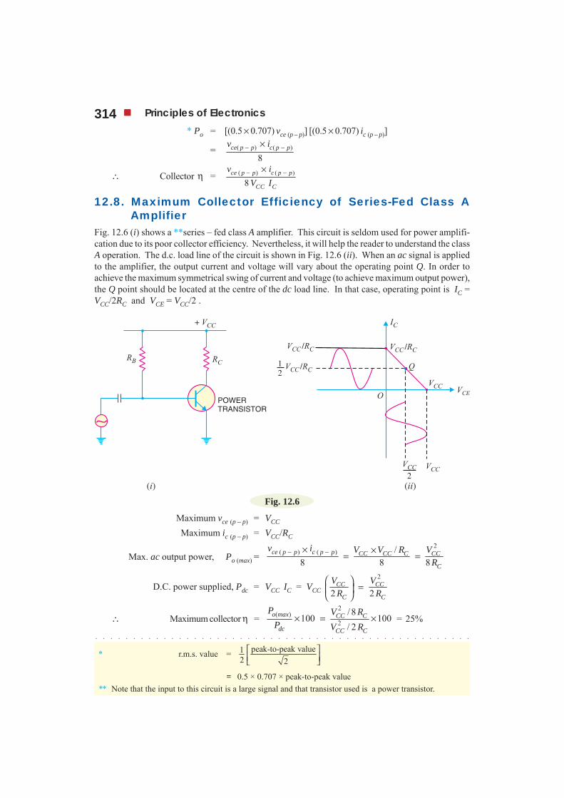
Fig. 12.6 (i) shows a **series – fed class A amplifier. This circuit is seldom used for power amplifi-cation due to its poor collector efficiency. Nevertheless, it will help the reader to understand the classA operation. The d.c. load line of the circuit is shown in Fig. 12.6 (ii). When an ac signal is appliedto the amplifier, the output current and voltage will vary about the operating point Q. In order toachieve the maximum symmetrical swing of current and voltage (to achieve maximum output power),the Q point should be located at the centre of the dc load line. In that case, operating point is IC =VCC/2RC and VCE = VCC/2 .
Fig. 12.6
Maximum vce (p − p) = VCC
Maximum ic (p − p) = VCC/RC
Max. ac output power, Po (max) =2
( ) ( ) /8 8 8
ce p p c p p CC CC C CC
C
v i V V R VR
− −× ×= =
D.C. power supplied, Pdc = VCC IC = VCC 2
2 2CC CC
C C
V VR R
⎛ ⎞=⎜ ⎟
⎝ ⎠
∴ Maximum collector η =2
( )2
/ 8100 100
/ 2o max CC C
dc CC C
P V RP V R
× = × = 25%
* r.m.s. value = peak-to-peak value12 2
⎡ ⎤⎢ ⎥⎣ ⎦
= 0.5 × 0.707 × peak-to-peak value** Note that the input to this circuit is a large signal and that transistor used is a power transistor.
Transistor Audio Power Amplifiers 315Thus the maximum collector efficiency of a class A series-fed amplifier is 25%. In actual practice,
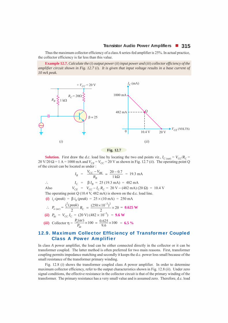
the collector efficiency is far less than this value.Example 12.7. Calculate the (i) output power (ii) input power and (iii) collector efficiency of the
amplifier circuit shown in Fig. 12.7 (i). It is given that input voltage results in a base current of10 mA peak.
Fig. 12.7
Solution. First draw the d.c. load line by locating the two end points viz., IC (sat) = VCC/RC =20 V/20 Ω = 1 A = 1000 mA and VCE = VCC = 20 V as shown in Fig. 12.7 (ii). The operating point Qof the circuit can be located as under :
IB = 20 0.71 k
CC BE
B
V VR− −=
Ω = 19.3 mA
∴ IC = β IB = 25 (19.3 mA) = 482 mAAlso VCE = VCC − IC RC = 20 V − (482 mA) (20 Ω) = 10.4 VThe operating point Q (10.4 V, 482 mA) is shown on the d.c. load line.(i) ic-(peak) = β ib (peak) = 25 × (10 mA) = 250 mA
∴ Po (ac) = 2 3 2( ) (250 10 ) 20
2 2c
Ci peak
R−×= × = 0.625 W
(ii) Pdc = VCC IC = (20 V) (482 × 10−3) = 9.6 W
(iii) Collector η = ( ) 0 625100 100
9 6× = ×o
dc
P ac .P . = 6.5 %
12.9. Maximum Collector Efficiency of Transformer CoupledClass A Power Amplifier
In class A power amplifier, the load can be either connected directly in the collector or it can betransformer coupled. The latter method is often preferred for two main reasons. First, transformercoupling permits impedance matching and secondly it keeps the d.c. power loss small because of thesmall resistance of the transformer primary winding.
Fig. 12.8 (i) shows the transformer coupled class A power amplifier. In order to determinemaximum collector efficiency, refer to the output characteristics shown in Fig. 12.8 (ii). Under zerosignal conditions, the effective resistance in the collector circuit is that of the primary winding of thetransformer. The primary resistance has a very small value and is assumed zero. Therefore, d.c. load
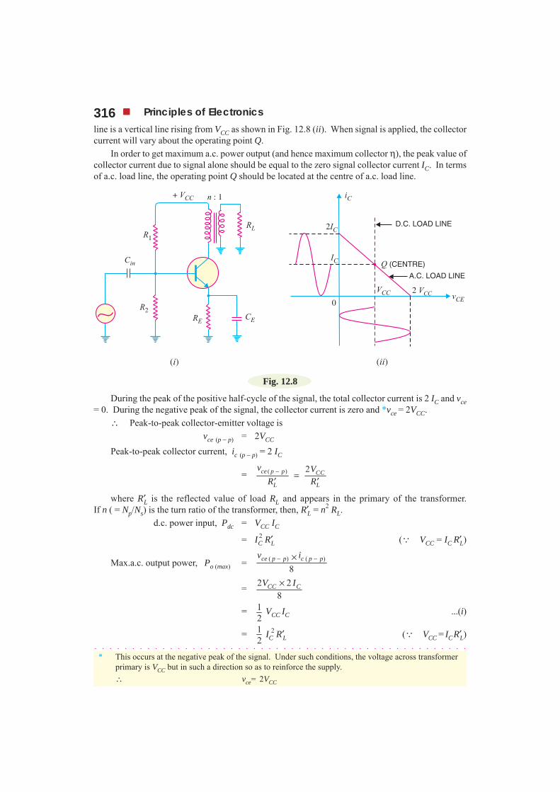
316 Principles of Electronics
line is a vertical line rising from VCC as shown in Fig. 12.8 (ii). When signal is applied, the collectorcurrent will vary about the operating point Q.
In order to get maximum a.c. power output (and hence maximum collector η), the peak value ofcollector current due to signal alone should be equal to the zero signal collector current IC. In termsof a.c. load line, the operating point Q should be located at the centre of a.c. load line.
Fig. 12.8
During the peak of the positive half-cycle of the signal, the total collector current is 2 IC and vce= 0. During the negative peak of the signal, the collector current is zero and *vce = 2VCC.
∴ Peak-to-peak collector-emitter voltage isvce (p − p) = 2VCC
Peak-to-peak collector current, ic (p − p) = 2 IC
= ( ) 2ce p p CC
L L
v VR R
− =′ ′
where R′L is the reflected value of load RL and appears in the primary of the transformer.If n ( = Np/Ns) is the turn ratio of the transformer, then, R′L = n2 RL.
d.c. power input, Pdc = VCC IC
= I 2C R′L (∵ VCC = IC R′L)
Max.a.c. output power, Po (max) = ( ) ( )
8ce p p c p pv i− −×
= 2 28×CC CV I
= 12
VCC IC ...(i)
= 12
IC2 R′L (∵ VCC = IC R′L)
* This occurs at the negative peak of the signal. Under such conditions, the voltage across transformerprimary is VCC but in such a direction so as to reinforce the supply.∴ vce= 2VCC
Transistor Audio Power Amplifiers 317
∴ Max. collector η = ( ) 100o max
dc
PP
×
=2
2(1/ 2) C L
C L
I RI R
′′
× 100 = 50%
12.10 Important Points About Class A Power Amplifier(i) A *transformer coupled class A power amplifier has a maximum collector efficiency of 50%
i.e., maximum of 50% d.c. supply power is converted into a.c. power output. In practice, theefficiency of such an amplifier is less than 50% (about 35%) due to power losses in theoutput transformer, power dissipation in the transistor etc.
(ii) The power dissipated by a transistor is given by :Pdis = Pdc − Pac
where Pdc = available d.c. powerPac = available a.c. power
Clearly, in class A operation, the transistor must dissipate less heat when signal is applied andtherefore runs cooler.
(iii) When no signal is applied to a class A power amplifier, Pac = 0.∴ Pdis = Pdc
Thus in class A operation, maximum power dissipation in the transistor occurs under zero signalconditions. Therefore, the power dissipation capability of a power transistor (for class A operation)must be atleast equal to the zero signal rating. For example, if the zero signal power dissipation of atransistor is 1 W, then transistor needs a rating of atleast 1W. If the power rating of the transistor isless than 1 W, it is likely to be damaged.
(iv) When a class A power amplifier is used in the final stage, it is called single ended class Apower amplifier.
Example 12.8. A power transistor working in class A operation has zero signal power dissipa-tion of 10 watts. If the a.c. output power is 4 watts, find :
(i) collector efficiency (ii) power rating of transistorSolution.
Zero signal power dissipation, Pdc = 10 Wa.c. power output, Po = 4 W
(i) Collector efficiency = 4100 10010
o
dc
PP
× = × = 40%
(ii) The zero signal power represents the worst case i.e. maximum power dissipation in a tran-sistor occurs under zero signal conditions.
∴ Power rating of transistor = 10 WIt means to avoid damage, the transistor must have a power rating of atleast 10 W.Example 12.9. A class A power amplifier has a transformer as the load. If the transformer has
a turn ratio of 10 and the secondary load is 100 Ω, find the maximum a.c. power output. Given thatzero signal collector current is 100 mA.
Solution.Secondary load, RL = 100 Ω
* However, resistance coupled class A power amplifier has a maximum collector efficiency of 25%.
318 Principles of Electronics
Transformer turn ratio, n = 10Zero signal collector current, IC = 100 mA
Load as seen by the primary of the transformer isR′L = n2 RL = (10)2 × 100 = 10,000 Ω
∴ Max. a.c. power output = ( )221 1 100 10,000
2 2 1000C LI R′ = ×
= 50 WExample 12.10. A class A transformer coupled power amplifier has zero signal collector cur-
rent of 50 mA. If the collector supply voltage is 5 V, find (i) the maximum a.c. power output (ii) thepower rating of transistor (iii) the maximum collector efficiency.
Solution.
(i) Max. a.c. power output, Po (max) = 2CC CV I
...See Art. 12.9
= (5 V) (50 mA)2
× = 125 mW
(ii) D.C input power, Pdc = VCC IC= (5 V) × (50 mA) = 250 mW
Since the maximum power is dissipated in the zero signal conditions,∴ Power rating of transistor = 250 mWThe reader may note that in class A operation :
Po(max) = 2disP
or Pdis = 2 Po (max)
It means that power rating of the transistor is twice as great as the maximum a.c. output power.For example, if a transistor dissipates 3 W under no signal conditions, then maximum a.c. outputpower it can deliver is 1.5 W.
(iii) Max. collector η = ( ) 125 mW100 100250 mW
o max
dc
PP
× = × = 50%
Example 12.11. In a certain transistor amplifier, ic (max) = 160 mA, ic (min) = 10mA, vce (max) = 12Vand vce (min) = 2V. Calculate the a.c. output power.
Solution.
A.C. output power, Po = ( ) ( )
8ce p p c p pv i− −×
Here vce (p – p) = 12V – 2V = 10V ; ic (p–p) = 160 mA – 10 mA = 150 mA
∴ Po = 10 V ×150 mA8 = 187.5 mW
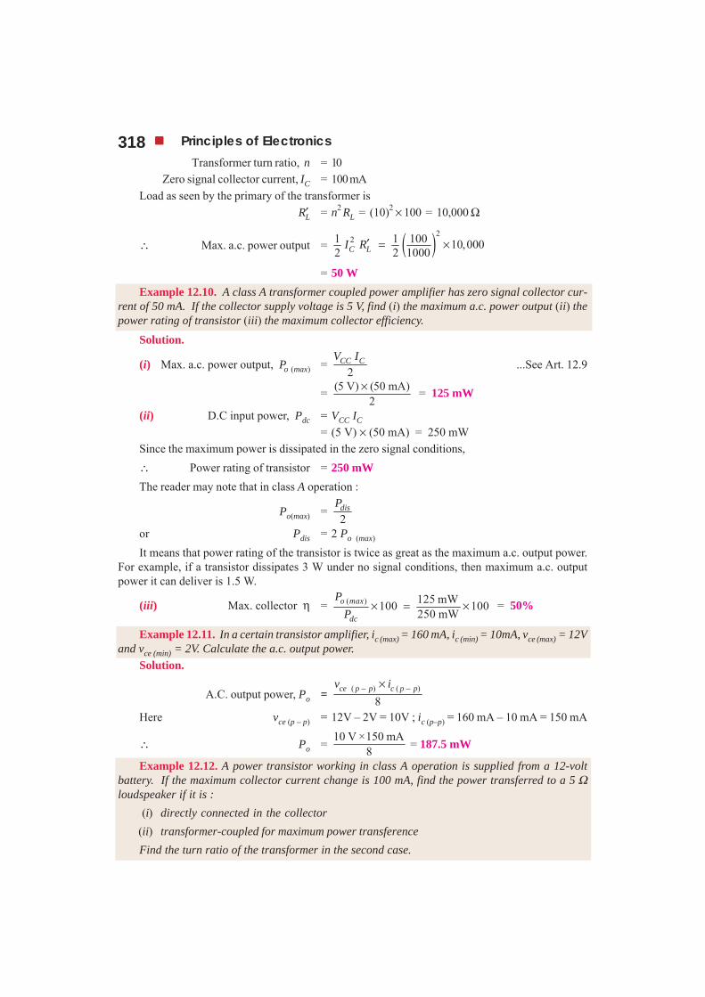
Example 12.12. A power transistor working in class A operation is supplied from a 12-voltbattery. If the maximum collector current change is 100 mA, find the power transferred to a 5 Ωloudspeaker if it is :
(i) directly connected in the collector(ii) transformer-coupled for maximum power transferenceFind the turn ratio of the transformer in the second case.
Transistor Audio Power Amplifiers 319Solution.
Max. collector current change, Δ IC = 100 mA
Max. collector-emitter voltage change is
Δ VCE = 12 V
Loudspeaker resistance, RL = 5 Ω
(i) Loudspeaker directly connected. Fig. 12.9 (i) shows the circuit of class A power amplifierwith loudspeaker directly connected in the collector.
Max. voltage across loudspeaker = Δ IC × RL = 100 mA × 5 Ω = 0.5 V
Power developed in the loudspeaker = 0.5 V × 100 mA= 0.05 W = 50 mW
Fig. 12.9
Therefore, when loudspeaker is directly connected in the collector, only 50 mW of power istransferred to the loudspeaker.
(ii) Loudspeaker transformer coupled. Fig. 12.9 (ii) shows the class A power amplifier withspeaker transformer coupled. As stated before, for impedance matching, step-down trans-former is used.
Output impedance of transistor =ΔΔ
CE
C
VI
= 12 V/100 mA = 120 Ω
In order to transfer maximum power, the primary resistance should be 120 Ω.Now, load R′L as seen by the primary is
R′L = n2 RL
or 120 = n2 RL
or n2 = 1205
∴ Turn ratio, n = 1205
= 4.9
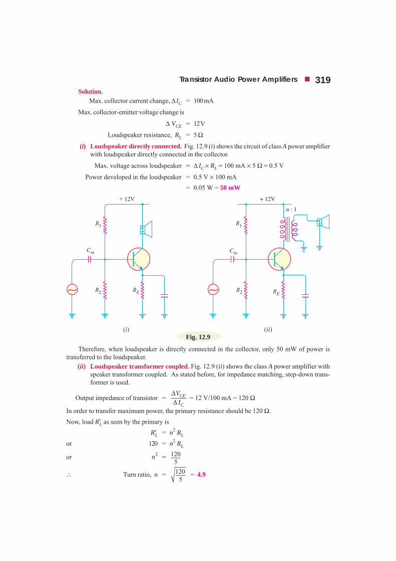
320 Principles of Electronics
Transformer secondary voltage
= Primary voltagen
= 12/4.9 = 2.47 V
Load current, IL = 2.47 V5 Ω = 0.49 A
Power transferred to the loudspeaker
= I2L RL
= (0.49)2 × 5 = 1.2 W = 1200 mWIt is clear that by employing transformer coupling, we have been able to transfer a large amount
of power (1200 mW) to the speaker. The main consideration in power amplifiers is the maximumpower output and, therefore, transformer coupling is invariably used.
Example 12.13. A common emitter class A transistor power amplifier uses a transistor with β =100. The load has a resistance of 81.6 Ω, which is transformer coupled to the collector circuit. If thepeak values of collector voltage and current are 30 V and 35 mA respectively and the correspondingminimum values are 5 V and 1 mA respectively, determine :
(i) the approximate value of zero signal collector current(ii) the zero signal base current
(iii) Pdc and Pac (iv) collector efficiency (v) turn ratio of the transformer.Solution.In an ideal case, the minimum values of vCE (min) and iC (min) are zero. However, in actual practice,
such ideal conditions cannot be realised. In the given problem, these minimum values are 5 V and1mA respectively as shown in Fig. 12.10.
Fig. 12.10
(i) The zero signal collector current is approximately half-way between the maximum and mini-mum values of collector current i.e.
Zero signal IC = 35 1 12− + = 18 mA
(ii) Zero signal IB = IC / β = 18/100 = 0.18 mA
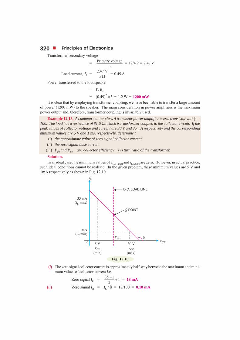
Transistor Audio Power Amplifiers 321
(iii) Zero signal VCE = 30 5 52− + = 17.5 V
Since the load is transformer coupled, VCC j 17.5 V.d.c. input power, Pdc = VCC IC = 17.5 V × 18 mA = 315 mW
a.c. output voltage, Vce = 30 52 2
− = 8.84 V
a.c. output current, Ic = 35 12 2
− = 12 mA
∴ a.c. output power, Pac = Vce × Ic= 8.84 V × 12 mA = 106 mW
(iv) Collector η = 106100 100315
× = ×ac
dc
PP = 33.7%
(v) The a.c. resistance R′L in the collector is determined from the slope of the line.
Slope =35 1 341 kilo mho5 30 25LR
− −− = =−′
∴ R ′L = 25 25k 100034 34
Ω = × = 735 Ω
∴ Turn ratio, n = 73581.6
′=L
L
RR
= 3
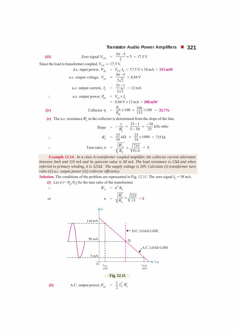
Example 12.14. In a class A transformer coupled amplifier, the collector current alternatesbetween 3mA and 110 mA and its quiscent value is 58 mA. The load resistance is 13Ω and whenreferred to primary winding, it is 325Ω. The supply voltage is 20V. Calculate (i) transformer turnratio (ii) a.c. output power (iii) collector efficiency.Solution. The conditions of the problem are represented in Fig. 12.11. The zero signal IC = 58 mA.
(i) Let n (= Np/Ns) be the turn ratio of the transformer.∴ R′L = n2 RL
or n =32513
L
L
RR
′= = 5
Fig. 12.11
(ii) A.C. output power, Pac = 212 C LI R′
322 Principles of Electronics
Heat Sink
* Almost the entire heat in a transistor is produced at the collector-base junction. If the temperature exceedsthe permissible limit, this junction is destroyed and the transistor is rendered useless.
** Most of power is dissipated at the collector-base junction. This is because collector-base voltage is muchgreater than the base-emitter voltage, although currents through the two junctions are almost the same.
= 12 (58 mA)2 × 325Ω = 546 mW
(iii) D.C. input power, Pdc = VCC IC = 20 V × 58 mA = 1160 mW
∴ Collector η = 546 1001160
× = 47%
12.11 Thermal RunawayAll semiconductor devices are very sensitive to temperature variations. If the temperature of a transis-tor exceeds the permissible limit, the transistor may be *permanently damaged. Silicon transistors canwithstand temperatures upto 250ºC while the germanium transistors can withstand temperatures upto100ºC.
There are two factors which determine the operating temperature of a transistor viz. (i) surround-ing temperature and (ii) power dissipated by the transistor.
When the transistor is in operation, almost the entire heat is produced at the collector-basejunction. This power dissipation causes the junction temperature to rise. This in turn increases thecollector current since more electron-hole pairs are generated due to the rise in temperature. Thisproduces an increased power dissipation in the transistor and consequently a further rise in tempera-ture. Unless adequate cooling is provided or the transistor has built-in temperature compensationcircuits to prevent excessive collector current rise, the junction temperature will continue to increaseuntil the maximum permissible temperature is exceeded. If this situation occurs, the transistor will bepermanently damaged.
The unstable condition where, owing to rise in temperature, the collector current rises andcontinues to increase is known as thermal runaway.
Thermal runaway must always be avoided. If it occurs, permanent damage is caused and thetransistor must be replaced.
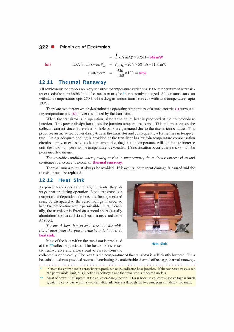
12.12 Heat SinkAs power transistors handle large currents, they al-ways heat up during operation. Since transistor is atemperature dependent device, the heat generatedmust be dissipated to the surroundings in order tokeep the temperature within permissible limits. Gener-ally, the transistor is fixed on a metal sheet (usuallyaluminium) so that additional heat is transferred to theAl sheet.
The metal sheet that serves to dissipate the addi-tional heat from the power transistor is known asheat sink.
Most of the heat within the transistor is producedat the **collector junction. The heat sink increasesthe surface area and allows heat to escape from thecollector junction easily. The result is that temperature of the transistor is sufficiently lowered. Thusheat sink is a direct practical means of combating the undesirable thermal effects e.g. thermal runaway.
Transistor Audio Power Amplifiers 323It may be noted that the ability of any heat sink to transfer heat to the surroundings depends upon itsmaterial, volume, area, shape, contact between case and sink and movement of air around the sink.Finned aluminium heat sinks yield the best heat transfer per unit cost.
It should be realised that the use of heat sink alone may not be sufficient to prevent thermalrunaway under all conditions. In designing a transistor circuit, consideration should also be given tothe choice of (i) operating point (ii) ambient temperatures which are likely to be encountered and (iii)the type of transistor e.g. metal case transistors are more readily cooled by conduction than plasticones. Circuits may also be designed to compensate automatically for temperature changes and thusstabilise the operation of the transistor components.
12.13 Mathematical AnalysisThe permissible power dissipation of the transistor is very important item for power transistors. Thepermissible power rating of a transistor is calculated from the following relation :
Ptotal =−θ
J max ambT T
where Ptotal = total power dissipated within the transistorTJ max = maximum junction temperature. It is 90ºC for germanium
transistors and 150ºC for silicon transistors.Tamb = ambient temperature i.e. temperature of surrounding air
θ = *thermal resistance i.e. resistance to heat flow from thejunction to the surrounding air
The unit of θ is ºC/ watt and its value is always given in the transistor manual. A low thermalresistance means that it is easy for heat to flow from the junction to the surrounding air. The larger thetransistor case, the lower is the thermal resistance and vice-versa. It is then clear that by using heatsink, the value of θ can be decreased considerably, resulting in increased power dissipation.
Example 12.15. A power transistor dissipates 4 W. If TJmax = 90ºC, find the maximum ambienttemperature at which it can be operated. Given θ = 10ºC/W.
Solution.Ptotal = 4 W
TJ max = 90ºCθ = 10ºC/W
Now Ptotal =−θ
J max ambT T
or 4 =90
10− ambT
∴ Ambient temperature, Tamb = 90 − 40 = 50ºCThe above example shows the effect of ambient temperature on the permissible power dissipa-
tion in a transistor. The lower the ambient temperature, the greater is the permissible power dissipa-tion. Thus, a transistor can pass a higher collector current in winter than in summer.
Example 12.16. (i) A power transistor has thermal resistance θ = 300ºC/W. If the maximumjunction temperature is 90ºC and the ambient temperature is 30ºC, find the maximum permissiblepower dissipation.
* The path of heat flow generated at the collector-base junction is from junction to case, from case to sinkand from sink to atmosphere.
324 Principles of Electronics
(ii) If a heat sink is used with the above transistor, the value of θ is reduced to 60ºC/W. Find themaximum permissible power dissipation.
Solution.(i) Without heat sink
TJ max = 90ºCTamb = 30ºC
θ = 300ºC/W
∴ Ptotal = 90 30300
J max ambT T− −=θ = 0.2 W = 200 mW
(ii) With heat sinkTJ max = 90ºC
Tamb = 30ºCθ = 60ºC/W
∴ Ptotal = 90 3060
J max ambT T− −=θ
= 1 W = 1000 mW
It is clear from the above example that permissible power dissipation with heat sink is 5 times ascompared to the case when no heat sink is used.
Example 12.17. The total thermal resistance of a power transistor and heat sink is 20°C/W.The ambient temperature is 25°C and TJ max = 200°C. If VCE = 4 V, find the maximum collectorcurrent that the transistor can carry without destruction. What will be the allowed value of collectorcurrent if ambient temperature rises to 75°C ?
Solution.
Ptotal = 200 2520
Jmax ambT T− −=θ
= 8.75 W
This means that maximum permissible power dissipation of the transistor at ambient temperatureof 25°C is 8.75 W i.e.
VCE IC = 8.75∴ IC = 8.75/4 = 2.19 A
Again Ptotal = 200 7520
J max ambT T− −=θ
= 6.25 W
∴ IC = 6.25/4 = 1.56 AThis example clearly shows the effect of ambient temperature.
12.14 Stages of A Practical Power AmplifierThe function of a practical power amplifier is to amplify a weak signal until sufficient power is availableto operate a loudspeaker or other output device. To achieve this goal, a power amplifier has generallythree stages viz. voltage amplification stage, driver stage and output stage. Fig. 12.12 shows theblock diagram of a practical power amplifier.
Fig. 12.12
Transistor Audio Power Amplifiers 325(i) Voltage amplification stage. The signals found in practice have extremely low voltage level
(< 10 mV). Therefore, the voltage level of the weak signal is raised by two or more voltageamplifiers. Generally, RC coupling is employed for this purpose.
(ii) Driver stage. The output from the last voltage amplification stage is fed to the driver stage.It supplies the necessary power to the output stage. The driver stage generally employs classA transformer coupled power amplifier. Here, concentrated effort is made to obtain maxi-mum power gain.
(iii) Output stage. The output power from the driver stage is fed to the output stage. It is thefinal stage and feeds power directly to the speaker or other output device. The output stageis invariably transformer coupled and employs class B amplifiers in push-pull arrangement.Here, concentrated effort is made to obtain maximum power output.
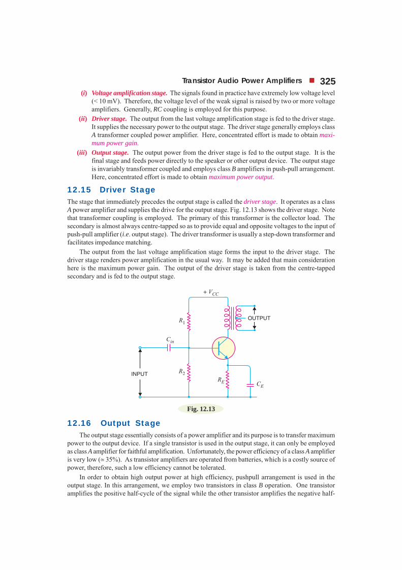
12.15 Driver StageThe stage that immediately precedes the output stage is called the driver stage. It operates as a classA power amplifier and supplies the drive for the output stage. Fig. 12.13 shows the driver stage. Notethat transformer coupling is employed. The primary of this transformer is the collector load. Thesecondary is almost always centre-tapped so as to provide equal and opposite voltages to the input ofpush-pull amplifier (i.e. output stage). The driver transformer is usually a step-down transformer andfacilitates impedance matching.
The output from the last voltage amplification stage forms the input to the driver stage. Thedriver stage renders power amplification in the usual way. It may be added that main considerationhere is the maximum power gain. The output of the driver stage is taken from the centre-tappedsecondary and is fed to the output stage.
Fig. 12.13
12.16 Output StageThe output stage essentially consists of a power amplifier and its purpose is to transfer maximum
power to the output device. If a single transistor is used in the output stage, it can only be employedas class A amplifier for faithful amplification. Unfortunately, the power efficiency of a class A amplifieris very low (j 35%). As transistor amplifiers are operated from batteries, which is a costly source ofpower, therefore, such a low efficiency cannot be tolerated.
In order to obtain high output power at high efficiency, pushpull arrangement is used in theoutput stage. In this arrangement, we employ two transistors in class B operation. One transistoramplifies the positive half-cycle of the signal while the other transistor amplifies the negative half-
326 Principles of Electronics
cycle of the signal. In this way, output voltage is a complete sine wave. At the same time, the circuitdelivers high output power to the load due to class B operation.
12.17 Push-Pull AmplifierThe push-pull amplifier is a power amplifier and is frequently employed in the output stages ofelectronic circuits. It is used whenever high output power at high efficiency is required. Fig. 12.14shows the circuit of a push-pull amplifier. Two tran-sistors Tr1 and Tr2 placed back to back are employed.Both transistors are operated in class B operation i.e.collector current is nearly zero in the absence of thesignal. The centre-tapped secondary of driver trans-former T1 supplies equal and opposite voltages to thebase circuits of two transistors.
The output transformer T2 has the centre-tappedprimary winding. The supply voltage VCC is connectedbetween the bases and this centre tap. The loud-speaker is connected across the secondary of thistransformer.
Circuit operation. The input signal appears acrossthe secondary AB of driver transformer. Suppose dur-ing the first half-cycle (marked 1) of the signal, end Abecomes positive and end B negative. This will makethe base-emitter junction of Tr1 reverse biased and that of Tr2 forward biased. The circuit will conductcurrent due to Tr2 only and is shown by solid arrows. Therefore, this half-cycle of the signal isamplified by Tr2 and appears in the lower half of the primary of output transformer. In the next half-cycle of the signal, Tr1 is forward biased whereas Tr2 is reverse biased. Therefore, Tr1 conducts and isshown by dotted arrows. Consequently, this half-cycle of the signal is amplified by Tr1 and appearsin the upper half of the output transformer primary. The centre-tapped primary of the output trans-former combines two collector currents to form a sine wave output in the secondary.
Fig. 12.14
It may be noted here that push-pull arrangement also permits a maximum transfer of power to theload through impedance matching. If RL is the resistance appearing across secondary of output trans-former, then resistance R′L of primary shall become :
Push-Pull Amplifier
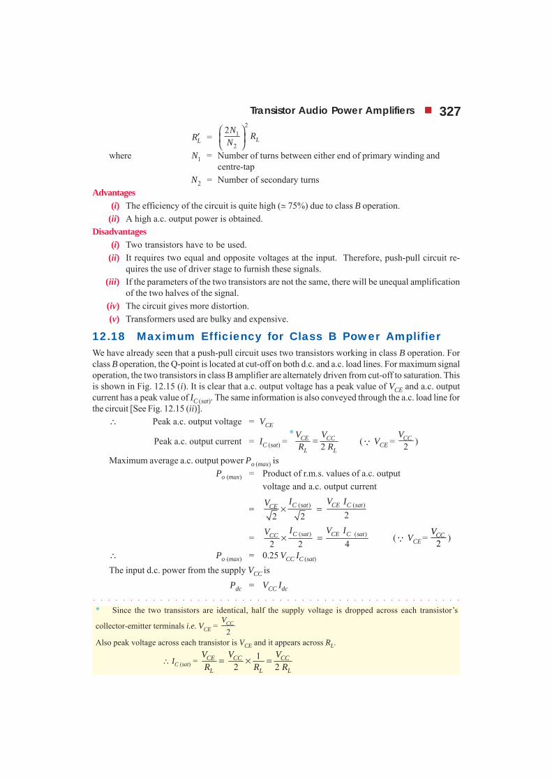
Transistor Audio Power Amplifiers 327
R′L =2
1
2
2⎛ ⎞⎜ ⎟⎝ ⎠
LN R
Nwhere N1 = Number of turns between either end of primary winding and
centre-tapN2 = Number of secondary turns
Advantages(i) The efficiency of the circuit is quite high (j 75%) due to class B operation.
(ii) A high a.c. output power is obtained.Disadvantages
(i) Two transistors have to be used.(ii) It requires two equal and opposite voltages at the input. Therefore, push-pull circuit re-
quires the use of driver stage to furnish these signals.(iii) If the parameters of the two transistors are not the same, there will be unequal amplification
of the two halves of the signal.(iv) The circuit gives more distortion.(v) Transformers used are bulky and expensive.
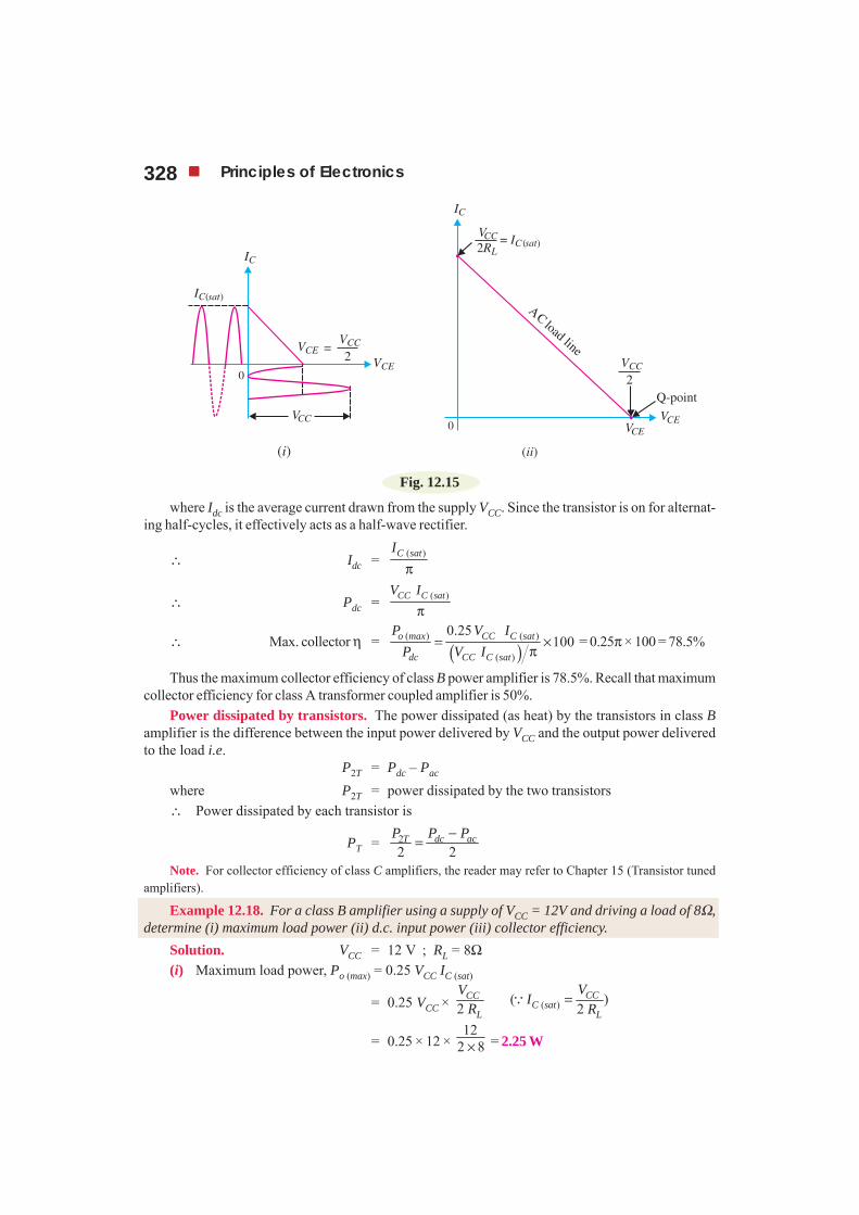
12.18 Maximum Efficiency for Class B Power AmplifierWe have already seen that a push-pull circuit uses two transistors working in class B operation. Forclass B operation, the Q-point is located at cut-off on both d.c. and a.c. load lines. For maximum signaloperation, the two transistors in class B amplifier are alternately driven from cut-off to saturation. Thisis shown in Fig. 12.15 (i). It is clear that a.c. output voltage has a peak value of VCE and a.c. outputcurrent has a peak value of IC (sat). The same information is also conveyed through the a.c. load line forthe circuit [See Fig. 12.15 (ii)].
∴ Peak a.c. output voltage = VCE
Peak a.c. output current = IC (sat) = *
2CE CC
L L
V VR R
= (∵ VCE = 2CCV
)
Maximum average a.c. output power Po (max) isPo (max) = Product of r.m.s. values of a.c. output
voltage and a.c. output current
= ( ) ( )
22 2× =C sat CE C satCE I V IV
= ( ) ( )
2 2 4× =C sat CE C satCC I V IV (∵ VCE = 2
CCV)
∴ Po (max) = 0.25 VCC IC (sat)
The input d.c. power from the supply VCC isPdc = VCC Idc
* Since the two transistors are identical, half the supply voltage is dropped across each transistor’s
collector-emitter terminals i.e. VCE = 2CCV
Also peak voltage across each transistor is VCE and it appears across RL.
∴ IC (sat) = 12 2
CE CC CC
L L L
V V VR R R
= × =
328 Principles of Electronics
Fig. 12.15
where Idc is the average current drawn from the supply VCC. Since the transistor is on for alternat-ing half-cycles, it effectively acts as a half-wave rectifier.
∴ Idc = ( )C satIπ
∴ Pdc = ( )CC C satV Iπ
∴ Max. collector η = ( )( ) ( )
( )
0.25100= ×
πo max CC C sat
dc CC C sat
P V IP V I
= 0.25π × 100 = 78.5%
Thus the maximum collector efficiency of class B power amplifier is 78.5%. Recall that maximumcollector efficiency for class A transformer coupled amplifier is 50%.
Power dissipated by transistors. The power dissipated (as heat) by the transistors in class Bamplifier is the difference between the input power delivered by VCC and the output power deliveredto the load i.e.
P2T = Pdc – Pac
where P2T = power dissipated by the two transistors∴ Power dissipated by each transistor is
PT = 22 2
−= dc acT P PP
Note. For collector efficiency of class C amplifiers, the reader may refer to Chapter 15 (Transistor tunedamplifiers).
Example 12.18. For a class B amplifier using a supply of VCC = 12V and driving a load of 8Ω,determine (i) maximum load power (ii) d.c. input power (iii) collector efficiency.
Solution. VCC = 12 V ; RL = 8Ω(i) Maximum load power, Po (max) = 0.25 VCC IC (sat)
= 0.25 VCC × 2CC
L
VR ( )( )
2CC
C satL
VI
R=∵
= 0.25 × 12 × 12
2 8× = 2.25 W
Transistor Audio Power Amplifiers 329
(ii) D.C. input power, Pdc =( )
2CC C sat CC CC
L
V I V VR
= ×π π
=12 12
2 8×
π × = 2.87 W
(iii) Collector η =( ) 2 25100 100
2 87o max
dc
P .P .
× = × = 78.4%
Example 12.19. A class B push-pull amplifier with transformer coupled load uses twotransistors rated 10 W each. What is the maximum power output one can obtain at the load from thecircuit?
Solution. The power dissipation by each transistor is PT = 10W. Therefore, power dissipated bytwo transistors is P2T = 2 × 10 = 20W.
Now Pdc = Po (max) + P2T ; Max. η = 0.785
∴ Max η =( ) ( ) ( )
( ) 2 ( ) 20o max o max o max
dc o max T o max
P P PP P P P
= =+ +
or 0.785 = ( )
( ) 20+o max
o max
PP
or 0.785 Po (max) + 15.7 = Po (max)
or Po (max) (1 – 0.785) = 15.7
∴ Po (max) =15 7 15 7
1 0 785 0 215. .. .
=− = 73.02 W
Example 12.20. A class B amplifier has an efficiency of 60% and each transistor has a ratingof 2.5W. Find the a.c. output power and d.c. input power
Solution. The power dissipated by each transistor is PT = 2.5W.Therefore, power dissipated by the two transistors is P2T = 2×2.5 = 5W.Now Pdc = Pac + P2T ; η = 0.6
∴ η =2
=+
ac ac
dc ac T
P PP P P
or 0.6 = 5+ac
ac
PP or 0.6 Pac + 3 = Pac
∴ Pac =3 3
1 0 6 0 4. .=
− = 7.5 W
and Pdc = Pac + P2T = 7.5 + 5 = 12.5 W
Example 12.21. A class B amplifier uses VCC = 10V and drives a load of 10Ω. Determine theend point values of the a.c. load line.
Solution.
IC (sat) =10V
2 2 (10 Ω)CC
L
VR
= = 500 mA
This locates one end-point of the a.c. load line on the collector current axis.
VCE (off) = 10V2 2CCV = = 5V
330 Principles of Electronics
This locates the second end-point of the a.c load line on the collector-emitter voltage axis. Byjoining these two points, the a.c. load line of the amplifier is constructed.
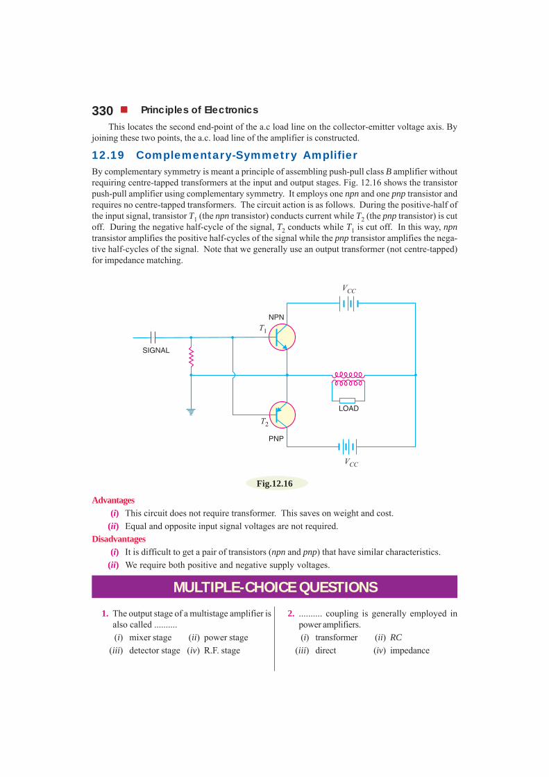
12.19 Complementary-Symmetry AmplifierBy complementary symmetry is meant a principle of assembling push-pull class B amplifier withoutrequiring centre-tapped transformers at the input and output stages. Fig. 12.16 shows the transistorpush-pull amplifier using complementary symmetry. It employs one npn and one pnp transistor andrequires no centre-tapped transformers. The circuit action is as follows. During the positive-half ofthe input signal, transistor T1 (the npn transistor) conducts current while T2 (the pnp transistor) is cutoff. During the negative half-cycle of the signal, T2 conducts while T1 is cut off. In this way, npntransistor amplifies the positive half-cycles of the signal while the pnp transistor amplifies the nega-tive half-cycles of the signal. Note that we generally use an output transformer (not centre-tapped)for impedance matching.
Fig.12.16
Advantages(i) This circuit does not require transformer. This saves on weight and cost.
(ii) Equal and opposite input signal voltages are not required.Disadvantages
(i) It is difficult to get a pair of transistors (npn and pnp) that have similar characteristics.(ii) We require both positive and negative supply voltages.
MULTIPLE-CHOICE QUESTIONS
1. The output stage of a multistage amplifier isalso called ..........(i) mixer stage (ii) power stage
(iii) detector stage (iv) R.F. stage
2. .......... coupling is generally employed inpower amplifiers.(i) transformer (ii) RC
(iii) direct (iv) impedance
Transistor Audio Power Amplifiers 3313. A class A power amplifier uses .......
(i) two transistors (ii) three transistors(iii) one transistor (iv) none of the above
4. The maximum efficiency of resistance loadedclass A power amplifier is ........(i) 78.5% (ii) 50%
(iii) 30% (iv) 25%5. The maximum efficiency of transformer
coupled class A power amplifier is .......(i) 30% (ii) 50%
(iii) 80% (iv) 45%6. Class ....... power amplifier has the highest
collector efficiency.(i) C (ii) A
(iii) B (iv) AB7. Power amplifiers handle ....... signals com-
pared to voltage amplifiers.(i) small (ii) very small
(iii) large (iv) none of the above8. In class A operation, the operating point is
generally located ........ of the d.c. load line.(i) at cut off point (ii) at the middle
(iii) at saturation point(iv) none of the above
9. Class C amplifiers are used as .........(i) AF amplifiers (ii) detectors
(iii) R.F. amplifiers (iv) none of the above10. A power amplifier has comparatively .........β.
(i) small (ii) large(iii) very large (iv) none of the above
11. The maximum collector efficiency of class Boperation is ........(i) 50% (ii) 90%
(iii) 60.5% (iv) 78.5%12. A 2-transistor class B power amplifier is com-
monly called ........ amplifier.(i) dual (ii) push-pull
(iii) symmetrical (iv) differential13. If a transistor is operated in such a way that
output current flows for 60º of the input sig-nal, then it is ...... operation.(i) class A (ii) class B
(iii) class C (iv) none of the above
14. If the zero signal power dissipation of a tran-sistor is 1 W, then power rating of the tran-sistor should be atleast ...........(i) 0.5 W (ii) 0.33 W
(iii) 0.75 W (iv) 1 W15. When a transistor is cut off, ........
(i) maximum voltage appears across tran-sistor
(ii) maximum current flows(iii) maximum voltage appears across load(iv) none of the above
16. A class A power amplifier is sometimescalled ........ amplifier.(i) symmetrical (ii) single-ended
(iii) reciprocating (iv) differential17. Class .......... operation gives the maximum
distortion.(i) A (ii) B
(iii) C (iv) AB18. The output stage of a multistage amplifier
usually employs ........(i) push-pull amplifier
(ii) preamplifier(iii) class A power amplifier(iv) none of the above
19. The size of a power transistor is made con-siderably large to ........(i) provide easy handling
(ii) dissipate heat(iii) facilitate connections(iv) none of the above
20. Low efficiency of a power amplifier resultsin .........(i) low forward bias
(ii) less battery consumption(iii) more battery consumption(iv) none of the above
21. The driver stage usually employs .......(i) class A power amplifier
(ii) push-pull amplifier(iii) class C amplifier(iv) none of the above
22. If the power rating of a transistor is 1 W andcollector current is 100 mA, then maximum
332 Principles of Electronics
allowable collector voltage is ........(i) 1 V (ii) 100 V
(iii) 20 V (iv) 10 V23. When no signal is applied, the approximate
collector efficiency of class A power ampli-fier is ...........(i) 10% (ii) 0%
(iii) 25% (iv) 50%24. What will be the collector efficiency of a
power amplifier having zero signal powerdissipation of 5 watts and a.c. power outputof 2 watts ?(i) 20% (ii) 80%
(iii) 40% (iv) 50%25. The output signal voltage and current of a
power amplifier are 5 V and 200 mA ; thevalues being r.m.s. What is the power out-put ?(i) 1 W (ii) 2 W
(iii) 4 W (iv) none of the above26. The maximum a.c. power output from a class
A power amplifier is 10 W. What should bethe minimum power rating of the transistorused ?(i) 10 W (ii) 15 W
(iii) 5 W (iv) 20 W27. For the same a.c. power output as above,
what should be the minimum power ratingof transistor for class B operation ?(i) 10 W (ii) 4 W
(iii) 8 W (iv) none of the above28. The push-pull circuit must use ..... operation.
(i) class A (ii) class C(iii) class B (iv) class AB
29. The class B push-pull circuit can deliver100 W of a.c. output power. What shouldbe the minimum power rating of eachtransistor ?(i) 20 W (ii) 40 W
(iii) 10 W (iv) 80 W30. What turn ratio (Np/Ns) of transformer is
required to match 4 Ω speaker to a transis-tor having an output impedance of 8000 Ω ?(i) 35.2 (ii) 44.7
(iii) 54.3 (iv) none of the above31. A transformer coupled class A power ampli-
fier has a load of 100 Ω on the secondary. Ifthe turn ratio is 10 : 1, what is the value ofload appearing on the primary ?(i) 5 kΩ (ii) 20 kΩ
(iii) 100 kΩ (iv) 10 kΩ32. Power amplifiers generally use transformer
coupling because transformer permits .......(i) cooling of the circuit
(ii) impedance matching(iii) distortionless output(iv) good frequency response
33. Transformer coupling can be used in ........amplifiers.(i) either power or voltage
(ii) only power(iii) only voltage (iv) none of the above
34. The output transformer used in a power am-plifier is a ...... transformer.(i) 1 : 1 ratio (ii) step-up
(iii) step-down (iv) none of the above35. The most important consideration in power
amplifiers is......(i) biasing the circuit
(ii) collector efficiency(iii) to keep the transformer cool(iv) none of the above
36. An AF amplifier is shielded to ........(i) keep the amplifier cool
(ii) protect from rusting(iii) prevent induction due to stray magnetic
fields(iv) none of the above
37. The pulsating d.c. applied to power ampli-fier causes ........(i) burning of transistor
(ii) hum in the circuit(iii) excessive forward voltage(iv) none of the above
38. The disadvantage of impedance matching isthat it ..........(i) gives distorted output
Transistor Audio Power Amplifiers 333(ii) gives low power output
(iii) requires a transformer(iv) none of the above
39. If the gain versus frequency curve of a tran-sistor amplifier is not flat, then there is .........distortion.
(i) amplitude (ii) intermodulation(iii) frequency (iv) none of the above
40. The most costly coupling is ............ coupling.(i) RC (ii) direct
(iii) impedance (iv) transformer.
Answers to Multiple-Choice Questions1. (ii) 2. (i) 3. (iii) 4. (iv) 5. (ii)6. (i) 7. (iii) 8. (ii) 9. (iii) 10. (i)
11. (iv) 12. (ii) 13. (iii) 14. (iv) 15. (i)16. (ii) 17. (iii) 18. (i) 19. (ii) 20. (iii)21. (i) 22. (iv) 23. (ii) 24. (iii) 25. (i)26. (iv) 27. (ii) 28. (iii) 29. (i) 30. (ii)31. (iv) 32. (ii) 33. (i) 34. (iii) 35. (ii)36. (iii) 37. (ii) 38. (i) 39. (iii) 40. (iv)
Chapter Review Topics1. What is an audio power amplifier ? What is its need ?2. Explain the difference between a voltage and a power amplifier.3. What do you understand by class A, class B and class C power amplifiers ?4. Define and explain the following terms as applied to power amplifiers :
(i) collector efficiency (ii) distortion (iii) power dissipation capability5. Show that maximum collector efficiency of class A transformer coupled power amplifier is 50%.6. Draw the block diagram of a practical power amplifier.7. Explain the push-pull circuit with a neat diagram.8. Write short notes on the following :
(i) Heat sink (ii) Driver stage(iii) Output stage (iv) Complementary-symmetry amplifier
Problems1. The resistance of the secondary of an output transformer is 100 Ω. If the output impedance is 10 kΩ,
find the turn ratio of the transformer for maximum power transference. [n = 10]2. A power transistor working in class A operation has zero signal power dissipation of 5 watts. If a.c.
output power is 2 watts, find (i) collector efficiency (ii) power rating of transistor.[(i) 40% (ii) 5 watts]
3. A class A power amplifier has a maximum a.c. power output of 30 W. Find the power rating of thetransistor. [60 W]
4. The a.c. power output of a class A power amplifier is 2 W. If the collector efficiency is 40%, find thepower rating of the transistor. [5 W]
5. In a class A transformer coupled amplifier, collector current alternates between 3 mA and 110 mA andits quiescent value is 58 mA. The load resistance is 15 Ω and when referred to primary winding is 325Ω. The supply voltage is 20V. Find (i) transformer turn ratio (ii) a.c. power output (iii) power ratingof transistor.
334 Principles of Electronics6. A transistor has thermal resistance θ = 80°C/W. If the maximum junction temperature is 90°C and the
ambient temperature is 30°C, find the maximum permissible power dissipation.[750 mW]
7. A power transistor dissipates 4 W. If TJ max = 90°C, find the maximum ambient temperature at whichit can be operated. Given thermal resistance θ = 8ºC/W. [58 °C]
8. A class A transformer-coupled amplifier uses a 25 : 1 transformer to drive a 4Ω load. Calculate theeffective a.c. load (seen by the transistor connected to the larger turns side of the transformer).
[2.5 kΩΩΩΩΩ]9. Calculate the transformer turns ratio required to connect 4 parallel 16Ω speakers so that they appear
as an 8 kΩ effective load. [44.7]10. For a class B amplifier with VCC = 25V driving an 8Ω load, determine :
(i) maximum input power(ii) maximum output power
(iii) maximum circuit efficiency[(i) 49.7W (ii) 39.06W (iii) 78.5 %]
Discussion Questions1. Why does collector efficiency play important part in power amplifiers ?2. Why does the problem of distortion arise in power amplifiers ?3. Why are power amplifiers classified on the basis of mode of operation ?4. Why does the output stage employ push-pull arrangement ?5. Why is driver stage necessary for push-pull circuit ?6. Why do we use transformer in the output stage ?


![[Gonzalez G.] Microwave Transistor Amplifiers Ana(BookFi.org)](https://img.pdfslide.net/doc/110x75/552df25d4a7959035a8b4838/gonzalez-g-microwave-transistor-amplifiers-anabookfiorg.jpg)