Embed Size (px)
Citation preview

SEPTEMBER 2010
DSC-5280/08 1
.
Features 128K x 36, 256K x 18 memory configurations Supports fast access times:
Commercial:– 7.5ns up to 117MHz clock frequency
LBO input selects interleaved or linear burst mode Self-timed write cycle with global write control (GW), byte write
enable (BWE), and byte writes (BWx) 3.3V core power supply Power down controlled by ZZ input 3.3V I/O Optional - Boundary Scan JTAG Interface (IEEE 1149.1
compliant) Packaged in a JEDEC Standard 100-pin plastic thin quad
flatpack (TQFP),
Pin Description Summary
NOTE:1. BW3 and BW4 are not applicable for the AS8C401825.
DescriptionTheAS8C403625/1825 are high-speed SRAMs organized as
128K x 36/256K x 18. The AS8C403625/1825 SRAMs contain write, data,address and control registers. There are no registers in the data outputpath (flow-through architecture). Internal logic allows the SRAM to gen-erate a self-timed write based upon a decision which can be left until theend of the write cycle.
The burst mode feature offers the highest level of performance to thesystem designer, as the AS8C403625/1825 can provide four cycles of datafor a single address presented to the SRAM. An internal burst addresscounter accepts the first cycle address from the processor, initiating theaccess sequence. The first cycle of output data will flow-through from thearray after a clock-to-data access time delay from the rising clock edge ofthe same cycle. If burst mode operation is selected (ADV=LOW), thesubsequent three cycles of output data will be available to the user on thenext three rising clock edges. The order of these three addresses aredefined by the internal burst counter and the LBO input pin.
The AS8C403625/1825 SRAMs utilize IDT’s latest high-performanceCMOS process and are packaged in a JEDEC standard 14mm x 20mm100-pin thin plastic quad flatpack (TQFP)
A0-A17 Address Inputs Input Synchronous
CE Chip Enable Input Synchronous
CS0, CS1 Chip Selects Input Synchronous
OE Output Enable Input Asynchronous
GW Global Write Enable Input Synchronous
BWE Byte Write Enable Input Synchronous
BW1, BW2, BW3, BW4(1) Individual Byte Write Selects Input Synchronous
CLK Clock Input N/A
ADV Burst Address Advance Input Synchronous
ADSC Address Status (Cache Controller) Input Synchronous
ADSP Address Status (Processor) Input Synchronous
LBO Linear / Interleaved Burst Order Input DC
TMS Test Mode Select Input Synchronous
TDI Test Data Input Input Synchronous
TCK Test Clock Input N/A
TDO Test Data Output Output Synchronous
TRST JTAG Reset (Optional) Input Asynchronous
ZZ Sleep Mode Input Asynchronous
I/O0-I/O31, I/OP1-I/OP4 Data Input / Output I/O Synchronous
VDD, VDDQ Core Power, I/O Power Supply N/A
VSS Ground Supply N/A
5280 tbl 01
128K X 36, 256K X 183.3V Synchronous SRAMs3.3V I/O, Flow-Through OutputsBurst Counter, Single Cycle Deselect
AS8C403625AS8C401825

6.422
AS8C403625, AS8C401825, 128K x 36, 256K x 18, 3.3V Synchronous SRAMs with3.3V I/O, Flow-Through Outputs, Burst Counter, Single Cycle Deselect Commercial Temperature Range
Pin Definitions(1)
NOTE:1. All synchronous inputs must meet specified setup and hold times with respect to CLK.
Symbol Pin Function I/O Active Description
A0-A17 Address Inputs I N/A Synchronous Address inputs. The address register is triggered by a combi-nation of the rising edge of CLKand ADSC Low or ADSP Low and CE Low.
ADSC Address Status(Cache Controller)
I LOW Synchronous Address Status from Cache Controller. ADSC is an active LOW input that is used to load theaddress registers with new addresses.
ADSP Address Status(Processor)
I LOW Synchronous Address Status from Processor. ADSP is an active LOW input that is used to load the addressregisters with new addresses. ADSP is gated by CE.
ADV Burst AddressAdvance
I LOW Synchronous Address Advance. ADV is an active LOW input that is used to advance the internal burst counter,controlling burst access after the initial address is loaded. When the input is HIGH the burst counter is notincremented; that is, there is no address advance.
BWE Byte Write Enable I LOW Synchronous byte write enable gates the byte write inputs BW1-BW4. If BWE is LOW at the rising edge of CLKthen BWx inputs are passed to the next stage in the circuit. If BWE is HIGH then the byte write inputs areblocked and only GW can initiate a write cycle.
BW1-BW4 Individual ByteWrite Enables
I LOW Synchronous byte write enables. BW1 controls I/O0-7, I/OP1, BW2 controls I/O8-15, I/OP2, etc. Any active bytewrite causes all outputs to be disabled.
CE Chip Enable I LOW Synchronous chip enable. CE is used with CS0 and CS1 to enable AS8C403625/1825. CE also gates ADSP.
CLK Clock I N/A This is the clock input. All timing references for the device are made with respect to this input.
CS0 Chip Select 0 I HIGH Synchronous active HIGH chip select. CS0 is used with CE and CS1 to enable the chip.
CS1 Chip Select 1 I LOW Synchronous active LOW chip select. CS1 is used with CE and CS0 to enable the chip.
GW Global WriteEnable
I LOW Synchronous global write enable. This input will write all four 9-bit data bytes when LOW on the rising edge ofCLK. GW supersedes individual byte write enables.
I/O0-I/O31
I/OP1-I/OP4
Data Input/Output I/O N/A Synchronous data input/output (I/O) pins. The data input path is registered, triggered by the rising edge ofCLK. The data output path is flow-through (no output register).
LBO Linear Burst Order I LOW Asynchronous burst order selection input. When LBO is HIGH, the inter-leaved burst sequence is selected.When LBO is LOW the Linear burst sequence is selected. LBO is a static input and must not change statewhile the device is operating.
OE Output Enable I LOW Asynchronous output enable. When OE is LOW the data output drivers are enabled on the I/O pins if the chipis also selected. When OE is HIGH the I/O pins are in a high-impedance state.
TMS Test ModeSelect I N/A Gives input command for TAP controller. Sampled on rising edge of TDK. This pin has an internal pullup.
TDI Test Data Input I N/ASerial input of registers placed between TDI and TDO. Sampled on rising edge of TCK. This pin has aninternal pullup.
TCK Test Clock I N/AClock input of TAP controller. Each TAP event is clocked. Test inputs are captured on rising edge of TCK,while test outputs are driven from the falling edge of TCK. This pin has an internal pullup.
TDO Test DataOutput O N/ASerial output of registers placed be tween TDI and TDO. This output is active depending on the state of theTAP controller.
TRSTJTAG Reset
(Optional)I LOW
Optional Asynchronous JTAG rese t. Can be used to reset the TAP contro ller, but not required. JTAG resetoccurs automatically at power up and also resets using TMS and TCK per IEEE 1149.1. If not used TRST canbe left floating. This pin has an internal pullup. Only available in BGA package.
ZZ Sleep Mode I HIGHAsynchronous sleep mode input. ZZ HIGH will gate the CLK internally and power down theAS8C403625/1825 to its lowest power consumption level. Data retention is guaranteed in Sleep Mode.This pin has an internal pulldown.
VDD Power Supply N/A N/A 3.3V core power supply.
VDDQ Power Supply N/A N/A 3.3V I/O Supply.
VSS Ground N/A N/A Ground.
NC No Connect N/A N/A NC pins are not electrically connected to the device.
5280 tbl 02

6.42AA
AS8C403625, AS8C401825, 128K x 36, 256K x 18, 3.3V Synchronous SRAMs with3.3V I/O, Flow-Through Outputs, Burst Counter, Single Cycle Deselect Commercial Temperature Range
3
Functional Block Diagram
A0 - A16/17 ADDRESSREGISTER
CLR A1*
A0*17/18
2
17/18
A2 - A17
128K x 36/256K x 18-
BITMEMORYARRAY
INTERNALADDRESS
A0,A1
BW4
BW3
BW2
BW1
Byte 1Write Register
36/18 36/18
ADSP
ADV
CLKADSC
CS0
CS1
Byte 1Write Driver
Byte 2Write Driver
Byte 3Write Driver
Byte 4Write Driver
Byte 2Write Register
Byte 3Write Register
Byte 4Write Register
9
9
9
9
GW
CE
BWE
LBO
I/O0 - I/O31I/OP1 - I/OP4
OE
DATA INPUTREGISTER
36/18
OUTPUTBUFFER
D QEnableRegister
OE
BurstSequenceCEN
CLK EN
CLK EN
Q1
Q0
2 BurstLogicBinary
Counter
5280 drw 01
ZZ Powerdown
,
JTAG(SA Version)
TMSTDITCKTRST
(Optional)
TDO

6.424
AS8C403625, AS8C401825 128K x 36, 256K x 18, 3.3V Synchronous SRAMs with3.3V I/O, Flow-Through Outputs, Burst Counter, Single Cycle Deselect Commercial Temperature Range
100 Pin TQFP Capacitance(TA = +25° C, f = 1.0mhz)
Recommended OperatingTemperature Supply Voltage
Absolute Maximum Ratings(1)
NOTES:1. Stresses greater than those listed under ABSOLUTE MAXIMUM RATINGS may
cause permanent damage to the device. This is a stress rating only and functionaloperation of the device at these or any other conditions above those indicatedin the operational sections of this specification is not implied. Exposure to absolutemaximum rating conditions for extended periods may affect reliability.
2. VDD terminals only.3. VDDQ terminals only.4. Input terminals only.5. I/O terminals only.6. This is a steady-state DC parameter that applies after the power supplies have
ramped up. Power supply sequencing is not necessary; however, the voltageon any input or I/O pin cannot exceed VDDQ during power supply ramp up.
7. TA is the "instant on" case temperature.
Recommended DC OperatingConditions
NOTES:1. VIH (max) = VDDQ + 1.0V for pulse width less than tCYC/2, once per cycle.2. VIL (min) = -1.0V for pulse width less than tCYC/2, once per cycle.
NOTE:1. This parameter is guaranteed by device characterization, but not production tested.
Symbol Rating Commercial &Industrial Values
Unit
VTERM(2) Terminal Voltage withRespect to GND
-0.5 to +4.6 V
VTERM(3,6) Terminal Voltage withRespect to GND
-0.5 to VDD V
VTERM(4,6) Terminal Voltage withRespect to GND
-0.5 to VDD +0.5 V
VTERM(5,6) Terminal Voltage withRespect to GND
-0.5 to VDDQ +0.5 V
TA(7)
CommercialOperating Temperature
-0 to +70 oC
IndustrialOperating Temperature
-40 to +85 oC
TBIAS TemperatureUnder Bias
-55 to +125 oC
TSTG StorageTemperature
-55 to +125 oC
PT Power Dissipation 2.0 W
IOUT DC Output Current 50 mA
5280 tbl 03
Grade Temperature(1) VSS VDD VDDQ
Commercial 0°C to +70°C 0V 3.3V±5% 3.3V±5%
Industrial -40°C to +85°C 0V 3.3V±5% 3.3V±5%
5280 tbl 04
Symbol Parameter Min. Typ. Max. Unit
VDD Core Supply Voltage 3.135 3.3 3.465 V
VDDQ I/O Supply Voltage 3.135 3.3 3.465 V
VSS Supply Voltage 0 0 0 V
VIH Input High Voltage - Inputs 2.0 ____ VDD +0.3 V
VIH Input High Voltage - I/O 2.0 ____ VDDQ +0.3(1) V
VIL Input Low Voltage -0.3(2) ____ 0.8 V
5280 tbl 06
Symbol Parameter(1) Conditions Max. Unit
CIN Input Capacitance VIN = 3dV 5 pF
CI/O I/O Capacitance VOUT = 3dV 7 pF
5280 tbl 07
NOTES:1. TA is the "instant on" case temperature.
119 BGA Capacitance(TA = +25° C, f = 1.0mhz)
Symbol Parameter(1) Conditions Max. Unit
CIN Input Capacitance VIN = 3dV 7 pF
CI/O I/O Capacitance VOUT = 3dV 7 pF
5280 tbl 07a
165 fBGA Capacitance(TA = +25° C, f = 1.0mhz)
Symbol Parameter(1) Conditions Max. Unit
CIN Input Capacitance VIN = 3dV 7 pF
CI/O I/O Capacitance VOUT = 3dV 7 pF
5280 tbl 07b

6.42
IDT71V3577, IDT71V3579, 128K x 36, 256K x 18, 3.3V Synchronous SRAMs with3.3V I/O, Flow-Through Outputs, Burst Counter, Single Cycle Deselect Commercial and Industrial Temperature Ran ges
5
Pin Configuration – 128K x 36
100 TQFPTop View
NOTES:1. Pin 14 does not have to be directly connected to VSS as long as the input voltage is < VIL.2. Pin 64 can be left unconnected and the device will always remain in active mode.
100 99 98 97 96 95 94 93 92 91 90 87 86 85 84 83 82 8189 88
123456789
10111213141516171819
2021222324252627282930
A6 A7 CE
CS0 BW4
BW3
BW2
BW1
CS1
VDD
VSS
CLK
GW
BWE
OE
ADSC
ADSP
ADV
A8 A9
NC
31 32 33 34 35 36 37 38 39 40 41 42 43 44 45 46 47 48 49 50
A16
NC
LBO
A14
A13
A12
A11
A10
VDD
VSSA0A1A2A3A4A5
I/OP4I/O31I/O30VDDQVSSI/O29I/O28I/O27I/O26VSS
VDDQI/O25I/O24
VSS(1)VDD
I/O23I/O22
VDDQVSSI/O21I/O20I/O19I/O18VSS
VDDQI/O17I/O16
I/OP3 80797877
76757473727170
696867666564
6362616059585756555453
5251
I/OP2
I/O14VDDQVSSI/O13I/O12I/O11I/O10
VSSVDDQI/O9I/O8VSSNCVDDZZ (2)
I/O7I/O6VDDQVSSI/O5
I/O4I/O3I/O2
VSSVDDQI/O1I/O0
I/OP1
VSS
I/O15
A15 5280 drw 02a
,NC
NC
NC

6.426
IDT71V3577, IDT71V3579, 128K x 36, 256K x 18, 3.3V Synchronous SRAMs with3.3V I/O, Flow-Through Outputs, Burst Counter, Single Cycle Deselect Commercial and Industrial Temperature Ra nges
Pin Configuration – 256K x 18
100 TQFPTop View
NOTES:1. Pin 14 does not have to be directly connected to VSS as long as the input voltage is < VIL.2. Pin 64 can be left unconnected and the device will always remain in active mode.
100 99 98 97 96 95 94 93 92 91 90 87 86 85 84 83 82 8189 88
12345678910111213141516171819
202122232425262728
2930
A6 A7 CE
CS0 NC
NC
BW2
BW1
CS1
VDD
VSS
CLK
GW BWE
OE
ADSC
ADSP
ADV
A8 A9
NC
31 32 33 34 35 36 37 38 39 40 41 42 43 44 45 46 47 48 49 50
A17
NCNC
LBO
A15
A14
A13
A12
A11
VDD
VSSA0A1A2A3A4A5
NCNCNC
VDDQVSSNC
I/OP2I/O15I/O14VSS
VDDQI/O13I/O12VSS
VDD
I/O11I/O10
VDDQVSSI/O9I/O8NCNCVSS
VDDQNCNCNC 80
797877
7675747372717069686766
656463626160595857565554535251
A10
NCVDDQVSSNCI/OP1I/O7I/O6VSSVDDQI/O5I/O4VSSNCVDDZZ(2)I/O3I/O2VDDQVSSI/O1
I/O0NCNCVSSVDDQNCNCNC
VSS(1)
NC
A16 5280 drw 02b
,
NC
NC

AS8C403625, AS8C401825, 128K x 36, 256K x 18, 3.3V Synchronous SRAMs with3.3V I/O, Flow-Through Outputs, Burst Counter, Single Cycle Deselect Commercial Temperature Range
7
DC Electrical Characteristics Over the OperatingTemperature and Supply Voltage Range (1)
DC Electrical Characteristics Over the OperatingTemperature and Supply Voltage Range (VDD = 3.3V ± 5%)
Figure 2. Lumped Capacitive Load, Typical Derating
Figure 1. AC Test Load
AC Test LoadAC Test Conditions(VDDQ = 3.3V)
NOTE:1. The LBO, TMS, TDI, TCK and TRST pins will be internally pulled to VDD and the ZZ in will be internally pulled to VSS if they are not actively driven in the application.
NOTES:1. All values are maximum guaranteed values.2. At f = fMAX, inputs are cycling at the maximum frequency of read cycles of 1/tCYC while ADSC = LOW; f=0 means no input lines are changing.3. For I/Os VHD = VDDQ - 0.2V, VLD = 0.2V. For other inputs VHD = VDD - 0.2V, VLD = 0.2V.
VDDQ/2
50Ω
I/O Z0 = 50Ω
5280 drw 03
,
Symbol Parameter Test Conditions Min. Max. Unit
|ILI| Input Leakage Current VDD = Max., VIN = 0V to VDD ___ 5 µA
|ILI| ZZ , LBO and JTAG Input Leakage Current(1) VDD = Max., VIN = 0V to VDD ___ 30 µA
|ILO| Output Leakage Current VOUT = 0V to VDDQ, Device Deselected ___ 5 µA
VOL Output Low Voltage IOL = +8mA, VDD = Min. ___ 0.4 V
VOH Output High Voltage IOH = -8mA, VDD = Min. 2.4 ___ V
5280 tbl 08
Symbol Parameter Test Conditions
7.5ns 8ns 8.5ns
UnitCom'l Only Com'l Ind Com'l Ind
IDD Operating Power Supply Current Device Se lected, Outputs Open, VDD = Max.,VDDQ = Max., VIN > VIH or < VIL, f = fMAX(2)
255 200 210 180 190 mA
ISB1 CMOS Standby PowerSupply Current
Device Deselected, Outputs Open, VDD = Max.,VDDQ = Max., VIN > VHD or < VLD, f = 0(2,3)
30 30 35 30 35 mA
ISB2 Clock Running PowerSupply Current
Device Deselected, Outputs Open, VDD = Max.,VDDQ = Max., VIN > VHD or < VLD, f = fMAX (2,.3)
90 85 95 80 90 mA
IZZ Full Sleep Mode Supply Current ZZ > VHD, VDD = Max. 30 30 35 30 35 mA
5280 tbl 09
Input Pulse Levels
Input Rise/Fall Times
Input Timing Reference Levels
Output Timing Reference Levels
AC Test Load
0 to 3V
2ns
1.5V
1.5V
See Figure 1
5280 tbl 10
1
2
3
4
20 30 50 100 200
∆tCD(Typical, ns)
Capacitance (pF)80
5
6
5280 drw 05
,

88
AS8C403625, AS8C401825, 128K x 36, 256K x 18, 3.3V Synchronous SRAMs with3.3V I/O, Flow-Through Outputs, Burst Counter, Single Cycle Deselect Commercial Temperature Range
Synchronous Truth Table (1,3)
NOTES:1. L = VIL, H = VIH, X = Don’t Care.2. OE is an asynchronous input.3. ZZ - low for the table.
Operation AddressUsed
CE CS0 CS1 ADSP ADSC ADV GW BWE BWx OE(2) CLK I/O
Deselected Cycle, Power Down None H X X X L X X X X X ↑ HI-Z
Deselected Cycle, Power Down None L X H L X X X X X X ↑ HI-Z
Deselected Cycle, Power Down None L L X L X X X X X X ↑ HI-Z
Deselected Cycle, Power Down None L X H X L X X X X X ↑ HI-Z
Deselected Cycle, Power Down None L L X X L X X X X X ↑ HI-Z
Read Cycle, Begin Burst External L H L L X X X X X L ↑ DOUT
Read Cycle, Begin Burst External L H L L X X X X X H ↑ HI-Z
Read Cycle, Begin Burst External L H L H L X H H X L ↑ DOUT
Read Cycle, Begin Burst External L H L H L X H L H L ↑ DOUT
Read Cycle, Begin Burst External L H L H L X H L H H ↑ HI-Z
Write Cycle, Begin Burst External L H L H L X H L L X ↑ DIN
Write Cycle, Begin Burst External L H L H L X L X X X ↑ DIN
Read Cycle, Continue Burst Next X X X H H L H H X L ↑ DOUT
Read Cycle, Continue Burst Next X X X H H L H H X H ↑ HI-Z
Read Cycle, Continue Burst Next X X X H H L H X H L ↑ DOUT
Read Cycle, Continue Burst Next X X X H H L H X H H ↑ HI-Z
Read Cycle, Continue Burst Next H X X X H L H H X L ↑ DOUT
Read Cycle, Continue Burst Next H X X X H L H H X H ↑ HI-Z
Read Cycle, Continue Burst Next H X X X H L H X H L ↑ DOUT
Read Cycle, Continue Burst Next H X X X H L H X H H ↑ HI-Z
Write Cycle, Continue Burst Next X X X H H L H L L X ↑ DIN
Write Cycle, Continue Burst Next X X X H H L L X X X ↑ DIN
Write Cycle, Continue Burst Next H X X X H L H L L X ↑ DIN
Write Cycle, Continue Burst Next H X X X H L L X X X ↑ DIN
Read Cycle, Suspend Burst Current X X X H H H H H X L ↑ DOUT
Read Cycle, Suspend Burst Current X X X H H H H H X H ↑ HI-Z
Read Cycle, Suspend Burst Current X X X H H H H X H L ↑ DOUT
Read Cycle, Suspend Burst Current X X X H H H H X H H ↑ HI-Z
Read Cycle, Suspend Burst Current H X X X H H H H X L ↑ DOUT
Read Cycle, Suspend Burst Current H X X X H H H H X H ↑ HI-Z
Read Cycle, Suspend Burst Current H X X X H H H X H L ↑ DOUT
Read Cycle, Suspend Burst Current H X X X H H H X H H ↑ HI-Z
Write Cycle, Suspend Burst Current X X X H H H H L L X ↑ DIN
Write Cycle, Suspend Burst Current X X X H H H L X X X ↑ DIN
Write Cycle, Suspend Burst Current H X X X H H H L L X ↑ DIN
Write Cycle, Suspend Burst Current H X X X H H L X X X ↑ DIN
5280 tbl 11

9
AS8C403625, AS8C401825, 128K x 36, 256K x 18, 3.3V Synchronous SRAMs with3.3V I/O, Flow-Through Outputs, Burst Counter, Single Cycle Deselect Commercial Temperature Range
9
Linear Burst Sequence Table ( LBO=VSS)
Synchronous Write Function Truth Table (1, 2)
Asynchronous Truth Table (1)
Interleaved Burst Sequence Table ( LBO=VDD)
NOTES:1. L = VIL, H = VIH, X = Don’t Care.2. BW3 and BW4 are not applicable for the AS8C401825.3. Multiple bytes may be selected during the same cycle.
NOTES:1. L = VIL, H = VIH, X = Don’t Care.2. Synchronous function pins must be biased appropriately to satisfy operation requirements.
NOTE:1. Upon completion of the Burst sequence the counter wraps around to its initial state.
NOTE:1. Upon completion of the Burst sequence the counter wraps around to its initial state.
Operation GW BWE BW1 BW2 BW3 BW4
Read H H X X X X
Read H L H H H H
Write all Bytes L X X X X X
Write all Bytes H L L L L L
Write Byte 1(3) H L L H H H
Write Byte 2(3) H L H L H H
Write Byte 3(3) H L H H L H
Write Byte 4(3) H L H H H L
5280 tbl 12
Operation(2) OE ZZ I/O Status Power
Read L L Data Out Active
Read H L High-Z Active
Write X L High-Z – Data In Active
Deselected X L High-Z Standby
Sleep Mode X H High-Z Sleep
5280 tbl 13
Sequence 1 Sequence 2 Sequence 3 Sequence 4
A1 A0 A1 A0 A1 A0 A1 A0
First Address 0 0 0 1 1 0 1 1
Second Address 0 1 0 0 1 1 1 0
Third Address 1 0 1 1 0 0 0 1
Fourth Address(1) 1 1 1 0 0 1 0 0
5280 tbl 14
Sequence 1 Sequence 2 Sequence 3 Sequence 4
A1 A0 A1 A0 A1 A0 A1 A0
First Address 0 0 0 1 1 0 1 1
Second Address 0 1 1 0 1 1 0 0
Third Address 1 0 1 1 0 0 0 1
Fourth Address(1) 1 1 0 0 0 1 1 0
5280 tbl 15

6.4210
AS8C403625,AS8C401825, 128K x 36, 256K x 18, 3.3V Synchronous SRAMs with3.3V I/O, Flow-Through Outputs, Burst Counter, Single Cycle Deselect Commercial Temperature Range
AC Electrical Characteristics(VDD = 3.3V ±5%, Commercial and Industrial Temperature Ranges)
7.5ns(5) 8ns 8.5ns
Symbol Parameter Min. Max. Min. Max. Min. Max. Unit
Clock Parameter
tCYC Clock Cycle Time 8.5 ____ 10 ____ 11.5 ____ ns
tCH(1) Clock High Pulse Width 3 ____ 4 ____ 4.5 ____ ns
tCL(1) Clock Low Pulse Width 3 ____ 4 ____ 4.5 ____ ns
Output Parameters
tCD Clock High to Valid Data ____ 7.5 ____ 8 ____ 8.5 ns
tCDC Clock High to Data Change 2 ____ 2 ____ 2 ____ ns
tCLZ(2) Clock High to Output Active 0 ____ 0 ____ 0 ____ ns
tCHZ(2) Clock High to Data High-Z 2 3.5 2 3.5 2 3.5 ns
tOE Output Enable Access Time ____ 3.5 ____ 3.5 ____ 3.5 ns
tOLZ(2) Output Enable Low to Output Active 0 ____ 0 ____ 0 ____ ns
tOHZ(2) Output Enable High to Output High-Z ____ 3.5 ____ 3.5 ____ 3.5 ns
Set Up Times
tSA Address Setup Time 1.5 ____ 2 ____ 2 ____ ns
tSS Address Status Setup Time 1.5 ____ 2 ____ 2 ____ ns
tSD Data In Setup Time 1.5 ____ 2 ____ 2 ____ ns
tSW Write Setup Time 1.5 ____ 2 ____ 2 ____ ns
tSAV Address Advance Setup Time 1.5 ____ 2 ____ 2 ____ ns
tSC Chip Enable/Select Setup Time 1.5 ____ 2 ____ 2 ____ ns
Hold Times
tHA Address Hold Time 0.5 ____ 0.5 ____ 0.5 ____ ns
tHS Address Status Hold Time 0.5 ____ 0.5 ____ 0.5 ____ ns
tHD Data In Hold Time 0.5 ____ 0.5 ____ 0.5 ____ ns
tHW Write Hold Time 0.5 ____ 0.5 ____ 0.5 ____ ns
tHAV Address Advance Hold Time 0.5 ____ 0.5 ____ 0.5 ____ ns
tHC Chip Enable/Select Hold Time 0.5 ____ 0.5 ____ 0.5 ____ ns
Sleep Mode and Configuration Parameters
tZZPW ZZ Pulse Width 100 ____ 100 ____ 100 ____ ns
tZZR(3) ZZ Recovery Time 100 ____ 100 ____ 100 ____ ns
tCFG(4) Configuration Set-up Time 34 ____ 40 ____ 50 ____ ns
5280 tbl 16NOTES:1. Measured as HIGH above VIH and LOW below VIL.2. Transition is measured ±200mV from steady-state.3. Device must be deselected when powered-up from sleep mode.4. tCFG is the minimum time required to configure the device based on the LBO input. LBO is a static input and must not change during normal operation.5. Commercial temperature range only.

6.42
IDT71V3577, IDT71V3579, 128K x 36, 256K x 18, 3.3V Synchronous SRAMs with3.3V I/O, Flow-Through Outputs, Burst Counter, Single Cycle Deselect Commercial and Industrial Temperature Ran ges
13
NOTE
S:1.
O1
(Ax)
repr
esen
ts th
e fir
st o
utpu
t fro
m th
e ex
tern
al a
ddre
ss A
x. O
1 (A
y) re
pres
ents
the
first
out
put f
rom
the
exte
rnal
add
ress
Ay;
O2
(Ay)
repr
esen
ts th
e ne
xt o
utpu
t dat
a in
the
burs
t seq
uenc
eof
the
base
add
ress
Ay,
etc
. whe
re A
0 an
d A1
are
adv
anci
ng fo
r the
four
wor
d bu
rst in
the
sequ
ence
def
ined
by t
he st
ate
of th
e LB
O in
put.
2.ZZ
inpu
t is L
OW
and
LBO
is D
on't C
are
for t
his c
ycle
.3.
CS0
timin
g tra
nsiti
ons a
re id
entic
al b
ut in
verte
d to
the
CE a
nd C
S1 si
gnal
s. F
or e
xam
ple,
whe
n CE
and
CS1
are
LO
W o
n th
is w
avef
orm
, CS0
is H
IGH
.
Timing Waveform of Flow-Through Read Cycle (1,2)
tCHZ
tSA
tSCtHS
GW,B
WE,B
Wx
tSWtCL
tSAV
tHW
tHAV
CLK
AD
SP
AD
SC
(1)
ADDRES
S
tCYC
tCH
tHA
tHC
tOE
tOHZ
OE
tCD
tOLZ
O1(Ax)
DAT
AOUT
tCDC
O1(Ay)
O2(Ay)
O2(Ay)
AD
V
CE,C
S1
(Note3)
Flow
-through
Read
BurstFlow-throughRead
Output
Disabled
AxAy
tSS
O1(Ay)
O4(Ay)
O3(Ay)
(Burstwraps
around
toits
initialstate)
5280
drw06
AD
VHIGHsuspends
burst
,

6.4214
IDT71V3577, IDT71V3579, 128K x 36, 256K x 18, 3.3V Synchronous SRAMs with3.3V I/O, Flow-Through Outputs, Burst Counter, Single Cycle Deselect Commercial and Industrial Temperature Ra nges
O1(Az)
CLK
AD
SP
ADDRESS GW
AD
V
OE
DAT
AOUT
tCYC
tCH
tCL
tHA
tSW
tHW
tCLZ
Ax
Ay
Az
tHS
I1(Ay)
tSD
tHD
tOLZ
tCD
tCDC
DAT
AIN
(2)
tOE
O1(Az)
SingleRead
Flow
-throughBu
rstR
ead
Write
tOHZ
tSS tS
A
O3(Az)
O2(Az)
O4(Az)
O1(Ax)
5280
drw07
tCD
,
NOTE
S:1.
Dev
ice
is s
elec
ted
thro
ugh
entir
e cy
cle;
CE
and
CS1
are
LOW
, C
S0 is
HIG
H.
2.ZZ
inpu
t is
LO
W a
nd L
BO is
Don
't C
are
for
this
cyc
le.
3.O
1 (Ax
) rep
rese
nts t
he fir
st ou
tput
from
the e
xter
nal a
ddre
ss A
x. I1
(Ay)
repr
esen
ts th
e firs
t inpu
t from
the e
xter
nal a
ddre
ss A
y; O
1 (Az
) rep
rese
nts t
he fir
st ou
tput
from
the e
xter
nal a
ddre
ss A
z; O
2 (Az
) rep
rese
nts
the
next
out
put d
ata
in th
e bu
rst s
eque
nce
of th
e ba
se a
ddre
ss A
z, e
tc. w
here
A0
and
A1 a
re a
dvan
cing
for
the
four
wor
d bu
rst i
n th
e se
quen
ce d
efin
ed b
y th
e st
ate
of th
e LB
O in
put.
Timing Waveform of Combined Flow-Through Read and Write Cycles (1,2,3)
6.42
IDT71V3577, IDT71V3579, 128K x 36, 256K x 18, 3.3V Synchronous SRAMs with3.3V I/O, Flow-Through Outputs, Burst Counter, Single Cycle Deselect Commercial and Industrial Temperature Ran ges
15
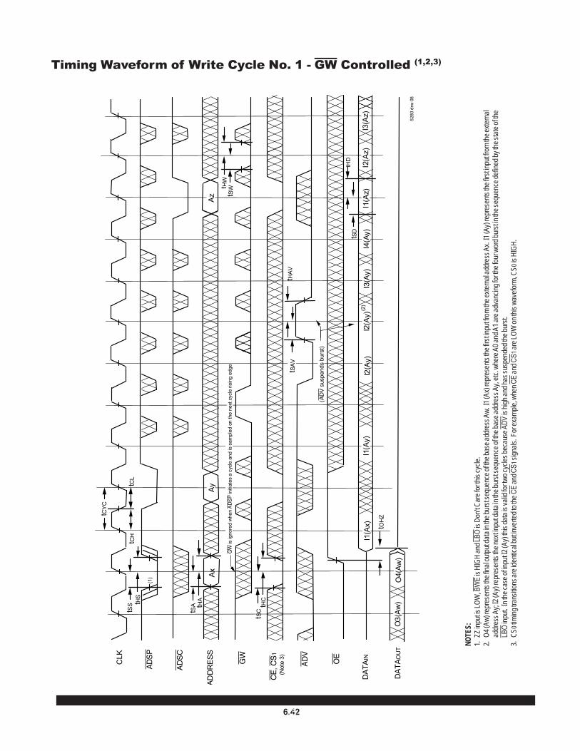
Timing Waveform of Write Cycle No. 1 - GW Controlled (1,2,3)
ADDRES
S
CLK
AD
SP
AD
SC
tCYC
tSS tH
StCH
tCL
tHA
tSA
AxAy
Az
AD
V
DAT
AOUT
OE
tHC
tSD
I1(Ax)
I1(Az)
I2(Ay)
tHD
tOHZ
DAT
AIN
tHAV
O4(Aw
)
CE,C
S1
tHW
GW
tSW
(Note3)
I2(Az)
I3(Az)
I4(Ay)
I3(Ay)
I2(Ay)
tSAV
(AD
Vsuspends
burst)
I1(Ay)
tSC
(1)
(2)
O3(Aw
)
5280
drw0 8
GWisignoredwhen
AD
SPinitiates
acycleandissampled
onthenextcyclerisingedge
,
NOTE
S:1.
ZZ in
put is
LO
W, B
WE
is H
IGH
and
LBO
is D
on't C
are
for t
his c
ycle
.2.
O4
(Aw
) rep
rese
nts t
he fin
al o
utpu
t dat
a in
the
burs
t seq
uenc
e of
the
base
add
ress
Aw
. I1
(Ax)
repr
esen
ts th
e fir
st in
put f
rom
the
exte
rnal
add
ress
Ax.
I1 (A
y) re
pres
ents
the
first
inpu
t fro
m th
e ex
tern
alad
dres
s Ay;
I2 (A
y) re
pres
ents
the
next
inpu
t dat
a in
the
burs
t seq
uenc
e of
the
base
add
ress
Ay,
etc
. whe
re A
0 an
d A1
are
adv
anci
ng fo
r the
four
wor
d bu
rst in
the
sequ
ence
def
ined
by t
he st
ate
of th
eLB
O in
put.
In th
e ca
se o
f inpu
t I2
(Ay)
this
dat
a is
valid
for t
wo
cycl
es b
ecau
se A
DV is
hig
h an
d ha
s sus
pend
ed th
e bu
rst.
3.C
S 0 tim
ing
trans
ition
s are
iden
tical
but
inve
rted
to th
e CE
and
CS1
sign
als.
For
exa
mpl
e, w
hen
CE a
nd C
S1 a
re L
OW
on
this
wav
efor
m, C
S0 is
HIG
H.

6.4216
IDT71V3577, IDT71V3579, 128K x 36, 256K x 18, 3.3V Synchronous SRAMs with3.3V I/O, Flow-Through Outputs, Burst Counter, Single Cycle Deselect Commercial and Industrial Temperature Ra nges
Timing Waveform of Write Cycle No. 2 - Byte Controlled (1,2,3)
ADDRES
S
CLK
ADSP
ADSC
tCYC
tSS tH
StCH
tCL
tHA
tSA
AxAy
tHW
BWx
ADV
DAT
AOUT
OE
tHC
tSD
Single
Write
BurstW
rite
I1(Ax)
I2(Ay)
I2(Ay)
I2(Az)
tHD
Burst
Read
Extended
BurstW
rite
tOHZ
DAT
AIN
tSAV
tSW
O4(Aw
)
CE,
CS1
tHW
BWE
tSW
(Note3)
I1(Az)
Az
I4(Ay)
I1(Ay)
I4(Ay)
I3(Ay)
tSC
BW
Eisignoredwhen
AD
SPinitiates
acycleandissampled
onthenextcyclerisingedge
BWxisignoredwhen
AD
SPinitiates
acycleandissampled
onthenextclockrisingedge
I3(Az)
O3(Aw
)
5280
drw09
(AD
VHIGHsuspends
burst)
,
NOTE
S:1.
ZZ in
put is
LO
W, G
W is
HIG
H a
nd LB
O is
Don
't Car
e fo
r thi
s cyc
le.
2.O
4 (A
w) r
epre
sent
s the
final
out
put d
ata
in th
e bu
rst s
eque
nce
of th
e ba
se a
ddre
ss A
w. I
1 (A
x) re
pres
ents
the
first
inpu
t fro
m th
e ex
tern
al a
ddre
ss A
x. I1
(Ay)
repr
esen
ts th
e fir
st in
put f
rom
the
exte
rnal
addr
ess A
y; I2
(Ay)
repr
esen
ts th
e ne
xt in
put d
ata
in th
e bu
rst s
eque
nce
of th
e ba
se a
ddre
ss A
y, e
tc. w
here
A0
and
A1 a
re a
dvan
cing
for t
he fo
ur w
ord
burs
t in th
e se
quen
ce d
efin
ed b
y the
stat
e of
the
LBO
inpu
t. In
the
case
of in
put I
2 (A
y) th
is d
ata
is va
lid fo
r tw
o cy
cles
bec
ause
ADV
is h
igh
and
has s
uspe
nded
the
burs
t.3.
CS0
timin
g tra
nsiti
ons a
re id
entic
al b
ut in
verte
d to
the
CE a
nd C
S1 si
gnal
s. F
or e
xam
ple,
whe
n CE
and
CS1
are
LO
W o
n th
is w
avef
orm
, CS0
is H
IGH
.

6.42
IDT71V3577, IDT71V3579, 128K x 36, 256K x 18, 3.3V Synchronous SRAMs with3.3V I/O, Flow-Through Outputs, Burst Counter, Single Cycle Deselect Commercial and Industrial Temperature Ran ges
17
tCYC
tSS
tCL
tCH
tHA
tSA
tSC
tHC
tOE
tOLZ
tHS
CLK
AD
SP
AD
SC
ADDRES
S
GW
CE
,CS1
AD
V
DAT
AOUT
OE ZZ
SingleRead
SnoozeMode
tZZP
W
5280
drw13
O1(Ax)
Ax
(Note4)
tZZR
Az
,
NOTE
S:1.
Dev
ice
mus
t pow
er u
p in
des
elec
ted
Mod
e.2.
LBO
is D
on't
Car
e fo
r thi
s cy
cle.
3. I
t is
not n
eces
sary
to re
tain
the
stat
e of
the
inpu
t reg
iste
rs th
roug
hout
the
Pow
er-d
own
cycl
e.4.
CS0
timin
g tra
nsiti
ons a
re id
entic
al b
ut in
verte
d to
the
CE a
nd C
S1 si
gnaa
ls. F
or e
xam
ple,
whe
n C
E an
d C
S1 a
re L
OW
on
this
wav
efor
m, C
S0 is
HIG
H.
Timing Waveform of Sleep (ZZ) and Power-Down Modes (1,2,3)

16
AS8C403625, AS8C401825, 128K x 36, 256K x 18, 3.3V Synchronous SRAMs with3.3V I/O, Flow-Through Outputs, Burst Counter, Single Cycle Deselect Commercial Temperature Range
NOTES:1. ZZ input is LOW, ADV is HIGH and LBO is Don't Care for this cycle.2. (Ax) represents the data for address Ax, etc.3. For read cycles, ADSP and ADSC function identically and are therefore interchangable.
Non-Burst Read Cycle Timing Waveform
CLK
ADSP
GW, BWE, BWx
CE, CS1
CS0
ADDRESS
ADSC
DATAOUT
OE
Av Aw Ax Ay Az
(Av) (Aw) (Ax) (Ay)
5280 drw 10 ,
Non-Burst Write Cycle Timing WaveformCLK
ADSP
GW
CE, CS1
CS0
ADDRESS
ADSC
DATAIN
Av Aw Ax AzAy
(Av) (Aw) (Ax) (Az)(Ay)
5280 drw 11
,NOTES:1. ZZ input is LOW, ADV and OE are HIGH, and LBO is Don't Care for this cycle.2. (Ax) represents the data for address Ax, etc.3. Although only GW writes are shown, the functionality of BWE and BWx together is the same as GW.4. For write cycles, ADSP and ADSC have different limitations.

17717172
AS8C403625, AS8C401825, 128K x 36, 256K x 18, 3.3V Synchronous SRAMs with3.3V I/O, Flow-Through Outputs, Burst Counter, Single Cycle Deselect Commercial Temperature Range
17
JTAG Interface Specification (SA Version only)
TCK
Device Inputs(1)/TDI/TMS
Device Outputs(2)/TDO
TRST(3)
tJCD
tJDC
tJRST
tJS tJH
tJCYC
tJRSR
tJF tJCLtJR
tJCH
M5280 drw 01x
Symbol Parameter Min. Max. Units
tJCYC JTAG Clock Input Period 100 ____ ns
tJCH JTAG Clock HIGH 40 ____ ns
tJCL JTAG Clock Low 40 ____ ns
tJR JTAG Clock Rise Time ____ 5(1) ns
tJF JTAG Clock Fall Time ____ 5(1) ns
tJRST JTAG Reset 50 ____ ns
tJRSR JTAG Reset Recovery 50 ____ ns
tJCD JTAG Data Output ____ 20 ns
tJDC JTAG Data Output Hold 0 ____ ns
tJS JTAG Setup 25 ____ ns
tJH JTAG Hold 25 ____ ns
I5280 tbl 01
Register Name Bit Size
Instruction (IR) 4
Bypass (BYR) 1
JTAG Identification (JIDR) 32
Boundary Scan (BSR) Note (1)
I5280 tbl 03
NOTES:1. Device inputs = All device inputs except TDI, TMS and TRST.2. Device outputs = All device outputs except TDO.3. During power up, TRST could be driven low or not be used since the JTAG circuit resets automatically. TRST is an optional JTAG reset.
NOTE:1. The Boundary Scan Descriptive Language (BSDL) file for this device is available
JTAG AC ElectricalCharacteristics(1,2,3,4)
Scan Register Sizes
NOTES:1. Guaranteed by design.2. AC Test Load (Fig. 1) on external output signals.3. Refer to AC Test Conditions stated earlier in this document.4. JTAG operations occur at one speed (10MHz). The base device may run at any speed specified in this datasheet.

2 18
AS8C403625, AS8C401825, 128K x 36, 256K x 18, 3.3V Synchronous SRAMs with3.3V I/O, Flow-Through Outputs, Burst Counter, Single Cycle Deselect Commercial Temperature Range
NOTES:1. Device outputs = All device outputs except TDO.2. Device inputs = All device inputs except TDI, TMS, and TRST.
Instruction Field Value Description
Revision Number (31:28) 0x2 Reserved for version number.
Device ID (27:12) 0x22C, 0x22E Defines AS8C403625/1825
JEDEC ID (11:1) 0x33 Allows unique identification of device vendor .
ID Register Indicator Bit (Bit 0) 1 Indicates the presence of an ID register.
I5280 tbl 02
JTAG Identification Register Definitions (SA Version only)
Instruction Description OPCODE
EXTESTForces contents of the boundary scan cells onto the device outputs(1).Places the boundary scan register (BSR) between TDI and TDO. 0000
SAMPLE/PRELOAD
Places the boundary scan register (BSR) between TDI and TDO.SAMPLE allows data from device inputs(2) and outputs(1) to be capturedin the boundary scan cells and shifted serially through TDO. PRELOADallows data to be input serially into the boundary scan cells via the TDI.
0001
DEVICE_IDLoads the JTAG ID register (JIDR) with the vendor ID code and placesthe register between TDI and TDO. 0010
HIGHZPlaces the bypass register (BYR) between TDI and TDO. Forces alldevice o utput drivers to a High-Z state. 0011
RESERVED
Several combinations are reserved. Do not use codes other than thoseidentified for EXTEST, SAMPLE/PRELOAD, DEVICE_ID, HIGHZ, CLAMP,VALIDATE and BYPASS instructions.
0100
RESERVED 0101
RESERVED 0110
RESERVED 0111
CLAMPUses BYR. Forces contents of the boundary scan cells onto the deviceoutputs. Places the bypass registe r (BYR) between TDI and TDO. 1000
RESERVED
Same as above.
1001
RESERVED 1010
RESERVED 1011
RESERVED 1100
VALIDATEAutomatically loaded into the instruction register whenever the TAPcontroller passes through the CAPTURE-IR state. The lower two bits '01'are mand ated by the IEEE std. 1149.1 specification.
1101
RESERVED Same as above. 1110
BYPASS The BYPASS instruction is used to truncate the boundary scan registeras a single bit in length.
1111
I5280 tbl 04
Available JTAG Instructions

192
AS8C403625, AS8C401825, 128K x 36, 256K x 18, 3.3V Synchronous SRAMs with3.3V I/O, Flow-Through Outputs, Burst Counter, Single Cycle Deselect Commercial Temperature Range
19
100-pin Plastic Thin Quad Flatpack (TQFP)119 Ball Grid Array (BGA)165 Fine Pitch Ball Grid Array (fBGA)
PF**BGBQ
DeviceType
Restricted hazardous substance deviceG
Alliance Organization VCCRange Package Operating Temp Speed
ns
AS8C403625-QC75N 256K x 36 3.1 - 3.4V 100 pin TQFP Comercial 0 - 70C 7.5 AS8C401825-QC75N 512K x 18 3.1 - 3.4V 100 pin TQFP Comercial 0 - 70C 7.5
ORDERING INFORMATION
ORDERING INFORMATION
Alliance Organization VCCRange Package Operating Temp Speedns
AS6C8016A -55ZIN 512K x 16 2.7 - 5.5V 44pin TSOP II Industrial ~ -40 C - 85 C 55
AS6C8016A -55BIN 512K x 16 2.7 - 5.5V 48ball FBGA Industrial ~ -40 C - 85 C 55
PART NUMBERING SYSTEM
ORDERING INFORMATION
ORDERING INFORMATION
Alliance Organization VCCRange Package Operating Temp Speedns
AS6C8016A -55ZIN 512K x 16 2.7 - 5.5V 44pin TSOP II Industrial ~ -40 C - 85 C 55
AS6C8016A -55BIN 512K x 16 2.7 - 5.5V 48ball FBGA Industrial ~ -40 C - 85 C 55
PART NUMBERING SYSTEM
AS6C 8016 -55 X X N
Device Number Package Option Temperature Range 80 = 8M Z - 44pin TSOP I = Industriallow power SRAM prefix 16 = x16 AccessTime B = 48ball TFBGA (-40 to + 85 C)
N = Lead Free RoHScompliant part
PART NUMBERING SYSTEM
AS8C
01= ZBT Q = 100 Pin TQFP Sync.
SRAM prefix 18= x18 36 = x36 25 = Flow- Thru
0 ~ 70C 7.5 ns N= Leadfree
40 = 4M 00 = Pipelined
Speed Device Conf. Mode Package Operating Temp N
®
Alliance Memory, Inc.551 Taylor way, suite#1, San Carlos, CA 94070Tel: 650-610-6800Fax: 650-620-9211www.alliancememory.com
Copyright © Alliance Memory
All Rights Reserved
Part Number: AS8C403625/401825
Document Version: v. 1.0
© Copyright 2003 Alliance Memory, Inc. All rights reserved. Our three-point logo, our name and Intelliwatt are trademarks or registered trademarks ofAlliance. All other brand and product names may be the trademarks of their respective companies. Alliance reserves the right to make changes to thisdocument and its products at any time without notice. Alliance assumes no responsibility for any errors that may appear in this document. The datacontained herein represents Alliance's best data and/or estimates at the time of issuance. Alliance reserves the right to change or correct this data at anytime, without notice. If the product described herein is under development, significant changes to these specifications are possible. The information inthis product data sheet is intended to be general descriptive information for potential customers and users, and is not intended to operate as, or provide,any guarantee or warrantee to any user or customer. Alliance does not assume any responsibility or liability arising out of the application or use of anyproduct described herein, and disclaims any express or implied warranties related to the sale and/or use of Alliance products including liability orwarranties related to fitness for a particular purpose, merchantability, or infringement of any intellectual property rights, except as express agreed to inAlliance's Terms and Conditions of Sale (which are available from Alliance). All sales of Alliance products are made exclusively according to Alliance'sTerms and Conditions of Sale. The purchase of products from Alliance does not convey a license under any patent rights, copyrights; mask works rights,trademarks, or any other intellectual property rights of Alliance or third parties. Alliance does not authorize its products for use as critical components inlife-supporting systems where a malfunction or failure may reasonably be expected to result in significant injury to the user, and the inclusion ofAlliance products in such life-supporting systems implies that the manufacturer assumes all risk of such use and agrees to indemnify Alliance against allclaims arising from such use.