Embed Size (px)
Citation preview
ELEGANT ALUS FROM SURFACE MOUNT SRAMS
A proposal submitted in partial fulfllment of the
requirements for the degree of
Doctor of Philosophy
by
Marc W Abel
BS California Institute of Technology 1991 γδβγ
2020
Wright State University
ABSTRACT
Marc W Abel Department of Computer Science and Engineering Wright State University 2020 Elegant ALUs from Surface Mount SRAMs
We consider the logic family comprised of separately packaged asynchronous
static RAMs for building computing systems requiring isolation from supply-chain
backdoors Static RAM is singular in its ability to operate as pure combinational logic
notwithstanding its high transistor count resulting in tremendous computational
elegance on one hand but no sequential enclaves to build a backdoor into on the
other hand Still further security beneft derives from SRAMrsquos fungibility low cost
assured absence of data when power is removed and limited input word size
Register fles control decoders and memory management units are
straightforward to produce using SRAM But a knowledge gap exists for arithmetic
logic units or ALUs It can be tempting to encode ldquotextbookrdquo ALUs into SRAM tables
but so doing throws away much computing power and speed It turns out that even
small ALUs can implement not just bitwise and additive logic but also fast rotations
and shifts with overfow detection subword transpositions and copies bit and prefx
counts foating point micro-operations short multiplication pointer realignments
minimum and maximum mixed-signedness comparisons mixed-signedness
arithmetic with overfow detection subword permutations and robust mixing
functions for hashing pseudorandom numbers and cryptography
An interesting duality emerges between the computation required of ALUs and
the structure of SRAM logic This duality tends to pull SRAM ALU designs into dense
elegant circuits with many symmetries surprising word size preferences and
unexpected speed The proposed research will specify test characterize and
disseminate a 36-bit ALU design that arises from these structures thereby
combining the robustness of computation ofered by SRAM ALUs with the ease of
manufacture and peace of mind they aford
ii
CONTENTS
1 Problem and approach 7
11 Manifesto on the security of CPUs 7
12 Practicality and economy of building CPUs 10
13 Logic family selection 11
14 SRAMs as electrical components 15
15 Proposalrsquos focus on ALUs 19
16 Questions for research 21
2 Essential logic blocks of SRAM ALUs 25
21 Hierarchy of ALU capabilities 25
22 Simple lookup elements 27
23 Arbitrary geometry adders 27
24 Carry-skip adders 28
25 Swizzlers 31
26 Logarithmic shifters 32
27 Semi-swizzlers 32
28 Substitution-permutation networks 33
29 Fast multipliers 33
3 2-layer ALU designs 38
31 An elegant 2-layer ALU for 36-bit words 38
32 A tiny ALU for 18-bit words 42
4 3-layer ALU designs 44
41 An elegant 3-layer ALU for 36-bit words 44
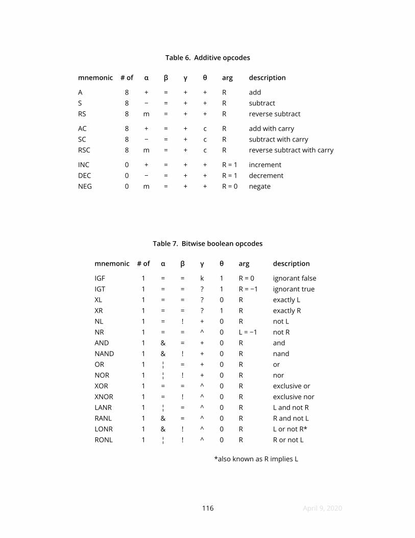
42 Additive opcodes 46
iii
43 Bitwise boolean opcodes 46
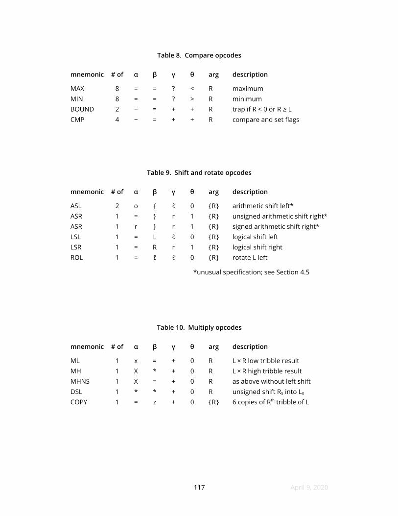
44 Compare opcodes 47
45 Shift and rotate opcodes 48
46 Multiply opcodes 49
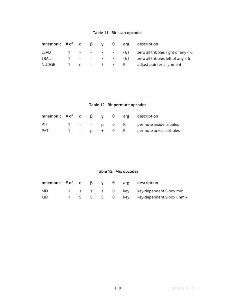
47 Bit scan opcodes 50
48 Bit permute opcodes 53
49 Mix opcodes 60
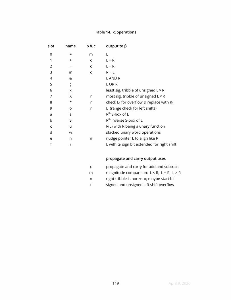
410 α layer operation 62
411 α layer operation leftmost tribble 65
412 β layer operation 65
413 γ layer operation 66
414 θ operation 68
415 Miscellaneous unary operations 69
416 Leading and trailing bit manipulation 72
5 Implications 73
51 Characteristics of surrounding CPU 73
52 Mixed signedness and practical overrange checks 81
53 Security 83
54 Anticipated performance 85
55 Suitable uses and limitations 86
56 Social and psychological beneft 88
57 Originality of research and contributions made 89
6 References 94
iv
PLATES
1 Simple lookup element
2 Arbitrary geometry addition
3 Subword carry decisions for 3-bit addition
4 2-layer carry-skip adder
5 2-layer carry-skip adder old carry via top
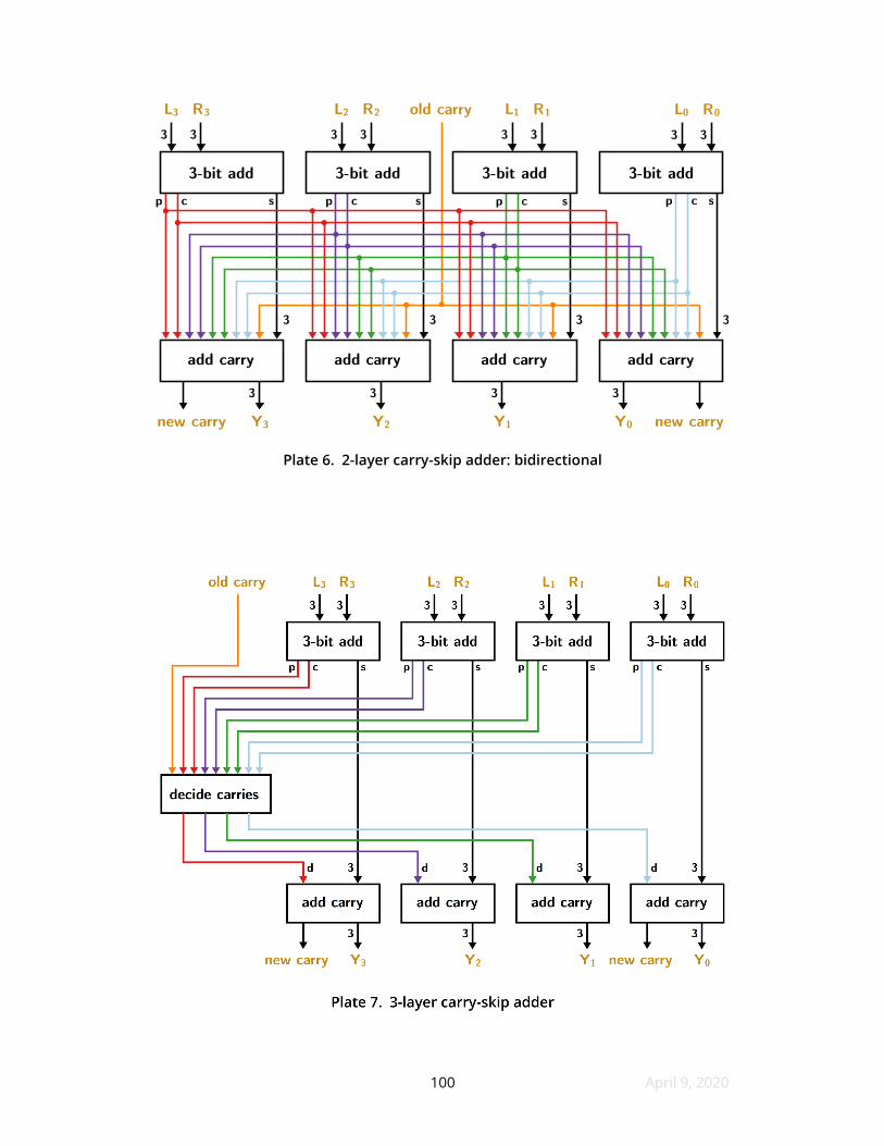
6 2-layer carry-skip adder bidirectional
7 3-layer carry-skip adder
8 4 times 4 swizzler
9 16-bit logarithmic shifter
10 4 times 4 semi-swizzler
11 4-bit S-box
12 16-bit substitution-permutation network
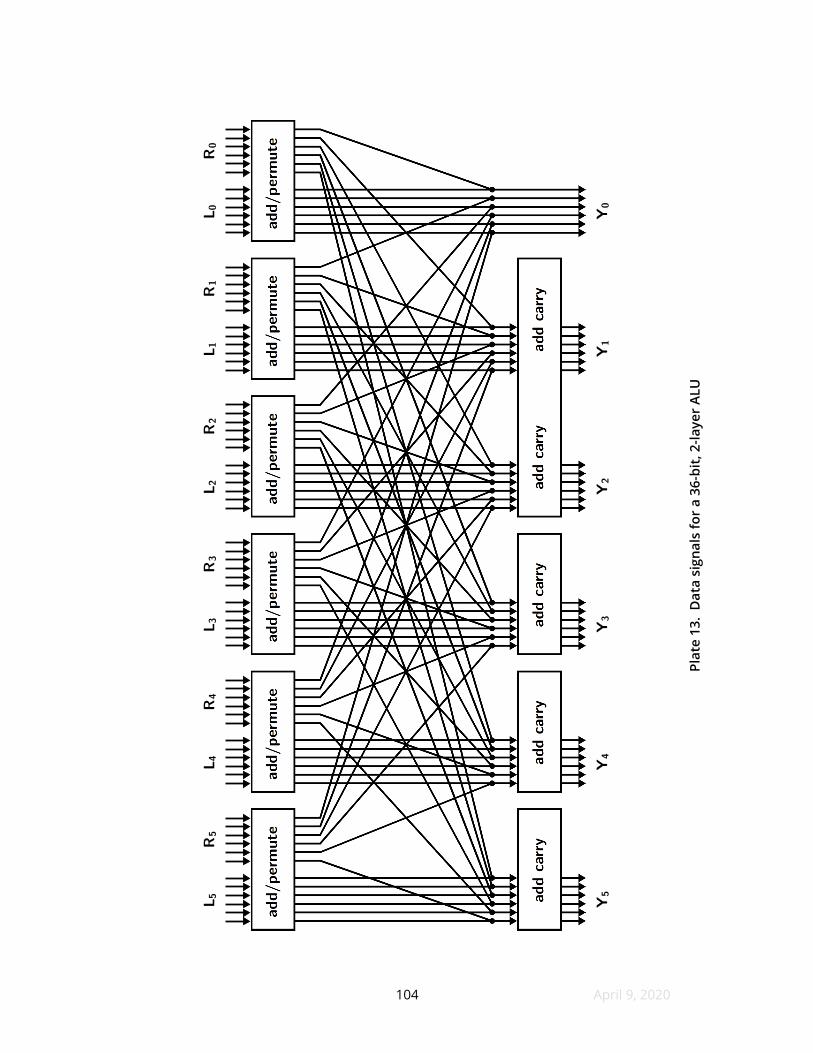
13 Data signals for a 36-bit 2-layer ALU
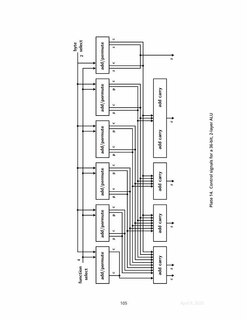
14 Control signals for a 36-bit 2-layer ALU
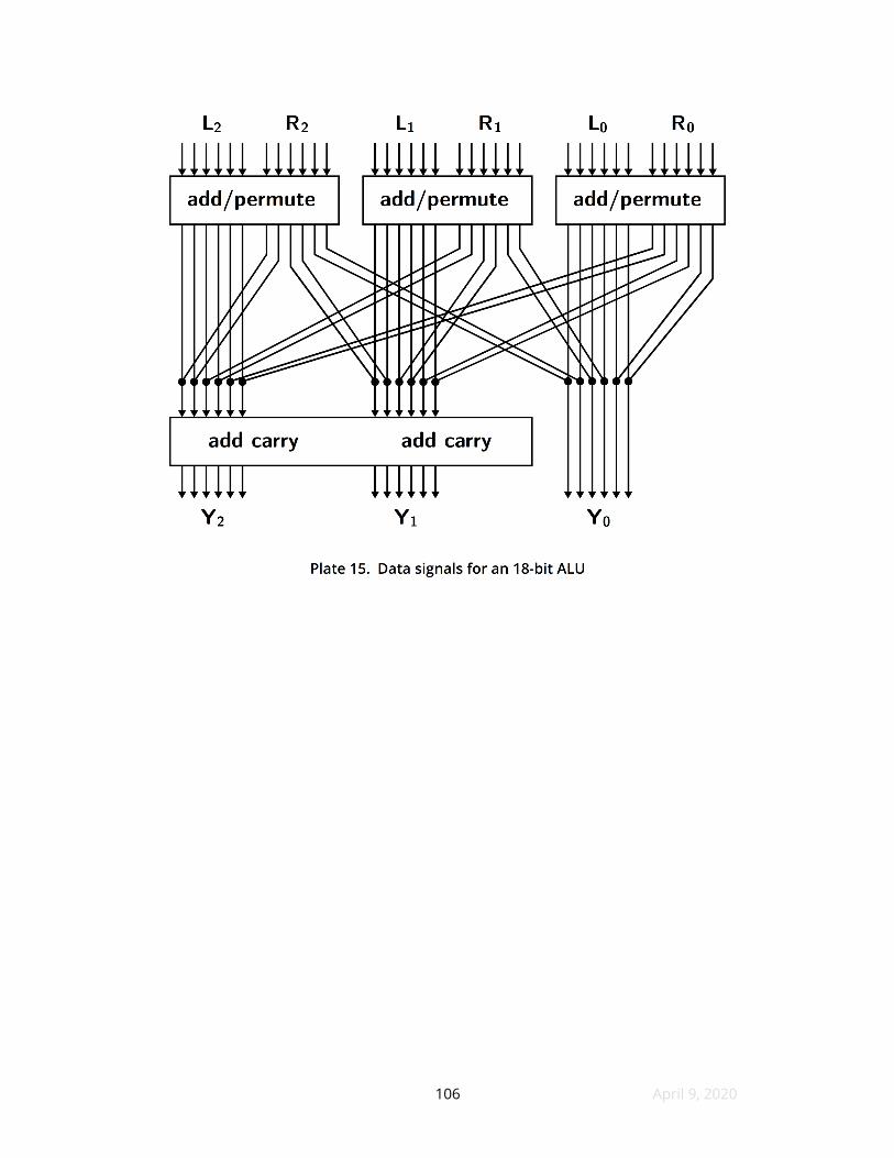
15 Data signals for an 18-bit ALU
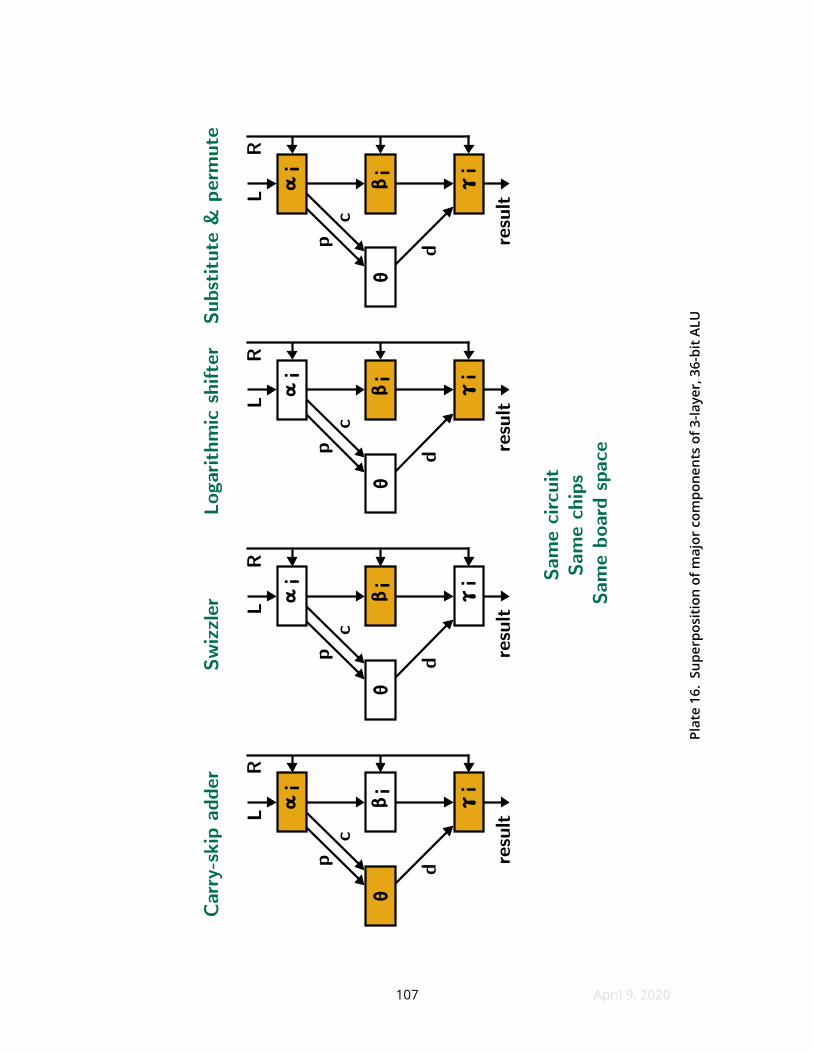
16 Superposition of major components of 3-layer 36-bit ALU
17 Block diagram of 36-bit ALU
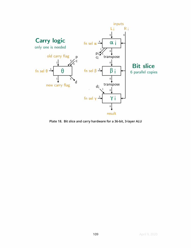
18 Bit slice and carry hardware for a 36-bit 3-layer ALU
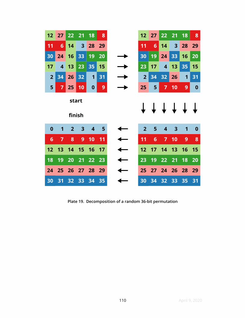
19 Decomposition of a random 36-bit permutation
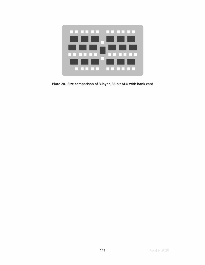
20 Size comparison of 3-layer 36-bit ALU with bank card
LISTINGS
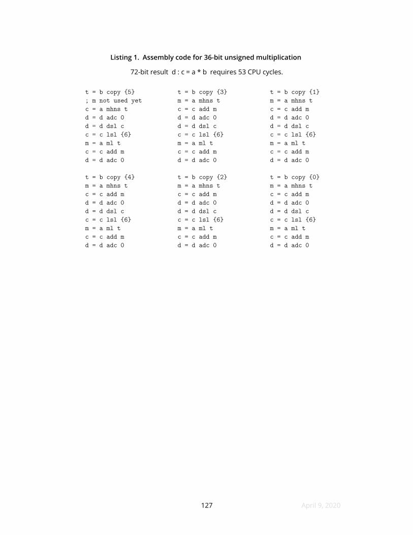
1 Assembly code for 36-bit unsigned multiplication
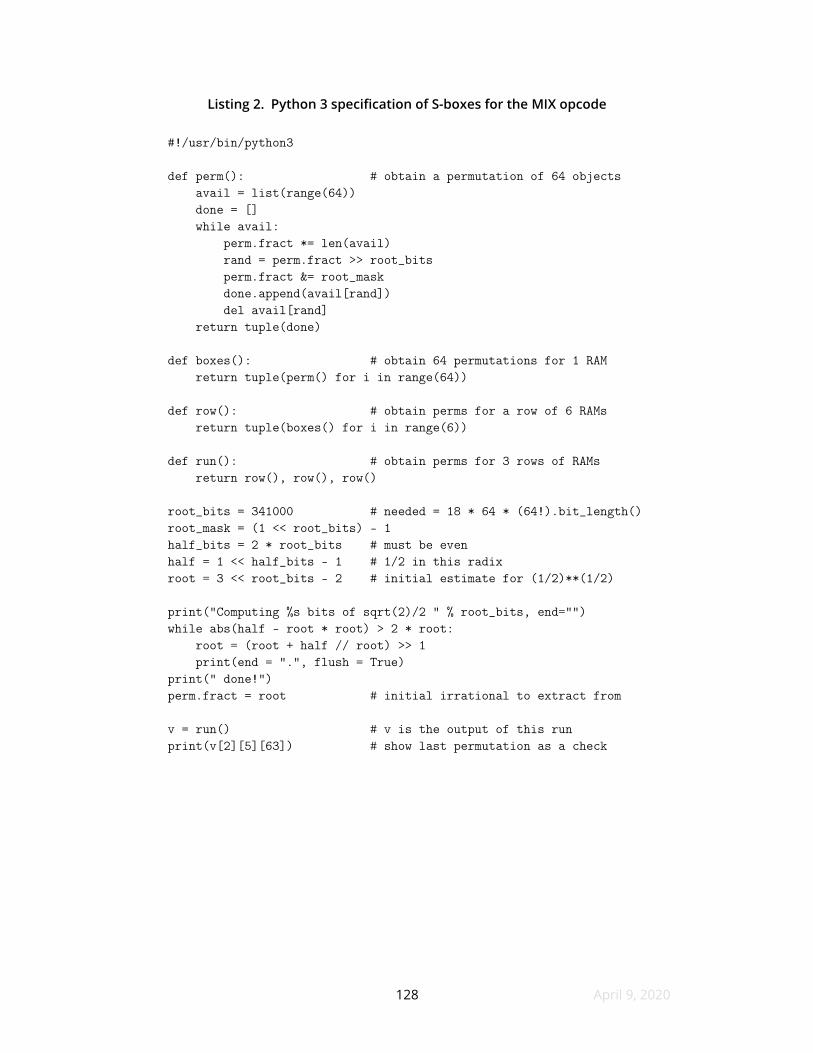
2 Python 3 specifcation of S-boxes for the MIX opcode
v
98
98
98
99
99
100
100
101
101
102
103
103
104
105
106
107
108
109
110
111
127
128
TABLES
1 Suggested operations for 36-bit 2-layer ALU
2 SRAM sizes for 36-bit 3-layer ALU
3 SRAM input bit assignments
4 SRAM output bit assignments
5 Opcode summary for 36-bit 3-layer ALU
6 Additive opcodes
7 Bitwise boolean opcodes
8 Compare opcodes
9 Shift and rotate opcodes
10 Multiply opcodes
11 Bit scan opcodes
12 Bit permute opcodes
13 Mix opcodes
14 α operations
15 α operations dealing with signedness
16 Propagate and carry encodings from α
17 β operations
18 γ operations
19 θ operations
20 Arithmetic overfow conditions
21 αu and γu unary operations
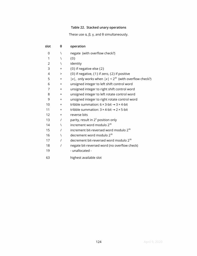
22 Stacked unary operations
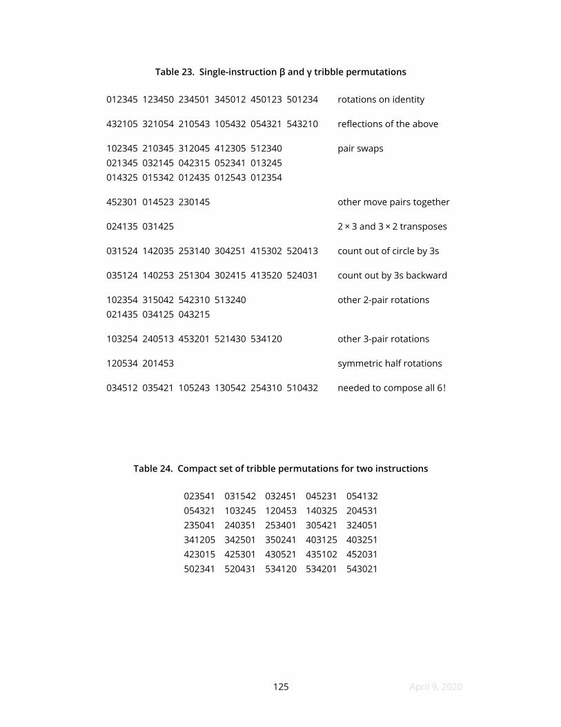
23 Single-instruction β and γ tribble permutations
24 Compact set of tribble permutations for two instructions
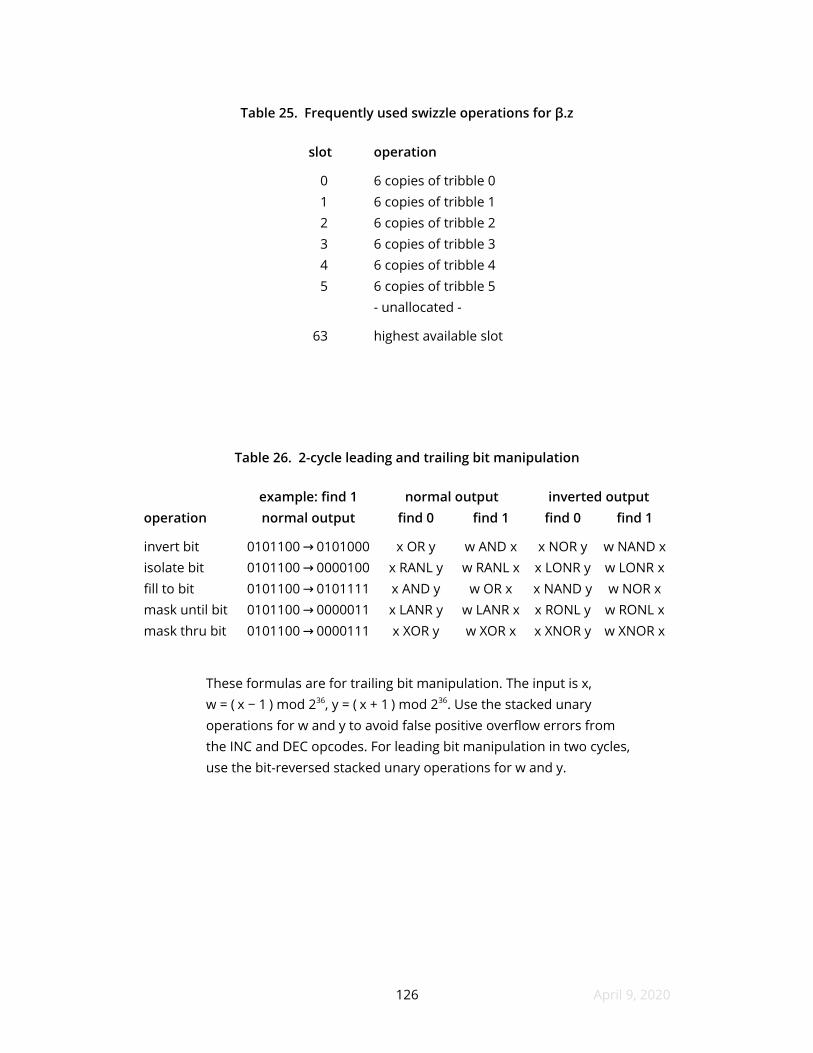
25 Frequently used swizzle operations for βz
26 2-cycle leading and trailing bit manipulation
vi
112
112
113
114
115
116
116
117
117
117
118
118
118
119
120
120
121
121
122
122
123
124
125
125
126
126
1 PROBLEM AND APPROACH
11 Manifesto on the security of CPUs
Herein is the privilege of being a computer scientist each of us has an
opportunity to identify technology that could bolster a specifc and preferably
humanitarian agenda and then seek out that technology and make it visible for
others A special interest I owe to my undergraduate faculty is demonstrable
correctness of computing implementations a property of paramount importance
thirty years later in the face of increasingly adversarial conditions
Much concern has been expressed recently about how the computing
hardware we use is designed and the immense attack surface that is now at our our
adversariesrsquo disposal as a consequence Irsquom not going to write much about this attack
surface as it is being extensively documented by others [1 2 3 4 5 6 7 8 9 10
11] Instead here is some work I can do in cooperation with my dissertation
committee to ofer a safer home for some of the worldrsquos automation computation
and communication
The security problems with todayrsquos silicon derive from root causes external to
the hardware itself We can talk about speculative execution pipelines cache misses
malformed input unstable memory schemes corrupt stacks arithmetic overfow
dopant-level trojans closed-source microcode open system buses proprietary
frmware counterfeit accessories and privilege escalation These technical
opportunities superpose with the human circumstances of globalization divergent
interests addiction to power situational ethics and economic inequality But I
believe the root problem with our CPUs is they are designed assembled and
distributed without input from the community that uses them If we hope to fnd
solutions for our security concerns a thoughtful look in a mirror might be a
promising start
A parallel malady has long existed in the software supply chain software
companies have been writing software for the purpose of selling it rather than out
7 April 9 2020
of their own need to have or use their wares The symptoms are all too familiar
needless changes and revisions made to already deployed software premature end
of support for widely used systems easily foreseen vulnerabilities cloud-based
licensing and subscription-only availability In many domains the open-source
software movement has aforded relief for some users In other domains much
remains to be accomplished I believe that on the whole community-sourced
software has brought unprecedented freedom security and stability to a world of
users I am also confdent that we can can achieve similar progress with CPUs
ofering stability security and freedom instead of obsolescence malfeasance and
monopolism
I can only speak on my own behalf but I think a consensus would exist that
CPUs for sensitive applications need to be demonstrably our own They must answer
to no one other than their owners exhibit no bad behaviors and have a feature set
that we fnd agreeable Here are some basic postulates of satisfactory CPUs
1 CPUs must not run operating systems Instead operating systems must
run CPUs
2 A CPU must not facilitate any exploit that can bypass any control of the
operating system that is running it
3 A CPU must run any and all adversary-supplied code without possibility
for privilege escalation1 never violating operating system permissions or
resource limits
4 Included and attached hardware as well as buses must not facilitate any
exploit that can bypass any control of an operating system that is
running a CPU
5 Attaching a CPU to a computer network must be no less secure than
keeping the CPU air gapped
6 A CPU must unconditionally protect all instruction pointers including
branch targets and subroutine return addresses
1 A regrettable exception is needed for social engineering attacks which by Ricersquos theorem cannot dependably be distinguished from fully mechanized attacks
8 April 9 2020
7 A CPUrsquos security must not be fragile in the presence of malformed input
8 A CPU must mitigate unanticipated modular arithmetic wrapping without
bloat inconvenience slowdown or incorrect results
9 A CPU must never give incorrect results merely due to unexpected
signedness or unsignedness of an operand
10 A CPU must support preemptive multitasking and memory protection
except for uses so simple that the application running and the operating
system are one and the same
11 A CPU must provide hashing pseudorandom number generation and
cryptography capabilities consistent with its intended use
12 A CPU must not depend in any manner on microcode updates for its
continued security or suitability for use
13 A CPU must be repairable by its owner particularly with regard to on-site
replacement of components or stored data that the owner might
foreseeably outlive
14 A CPU must be replaceable by its owner in its as-used form
15 A CPU must be delivered with objective verifable evidence of conformity
with these postulates
Simultaneously satisfying the above postulates is comfortably within human
intellect to accomplish I have two sorobans in my lab that generally meet the
parameters of this list even though they donrsquot use electricity to do arithmetic Two
TRS-80s here also run fne and although lacking conform closer to the above than
the 64-bit machine that this proposal was written on
Requirement 15 spawns two corollaries
16 All components of a CPU must be available afordable fungible and
inspectable
17 A CPU must not contain unknown undocumented unreadable or
unauditable circuitry frmware or microcode
9 April 9 2020
Fungible means if a component canrsquot be obtained from one supplier a diferent
component that will work equivalently can be obtained from a choice of suppliers
Inspectable means the manner of operation of a component can be verifed by the
owner in as much detail as desired
The requirements Irsquove laid out arenrsquot wistful parameters to secure this
committeersquos go-ahead for investigative daydreaming I have identifed specifc
constructible elegant mechanisms for such needs as memory protection arithmetic
wrap-around efcient hash functions and alternatives for electrolytic capacitors
Not all are within the scope of this proposal but I stand ready to back up all of this
documentrsquos functional demands
If our suppliers arenrsquot ready to assent to the above postulates we can build
superb CPUs independently But citizen-builders need to be prepared to trade away
two things First our CPU designs will depart from historic norms They wonrsquot run
MacOS or Microsoft Windows They wonrsquot play DRM-protected copies of Angry Birds
They might never run OpenBSD or Android and I hope they wonrsquot become
compilation targets for GCC or LLVM as neither is small enough to plausibly audit
against backdoors But if users commit to this concession suitable operating
systems toolchains and tools will appear
The second concession we need to build our own CPUs concerns their
dimensional quantities We wonrsquot get the speed energy efciency memory density
economy word size or parallelism that a semiconductor fab delivers Instead wersquoll
get security and ownership characteristics that we need more than these
dimensional quantities The dimensions are merely numbers and as long as our
CPUs are suitable and efective as used it doesnrsquot matter what their performance
metrics come to As a computer-literate undergraduate I was content to read my
email on a VAX I didnrsquot need to know that its clock speed was 3125 kilohertz
12 Practicality and economy of building CPUs
Building a CPU requires an assembly process we can manage and components
10 April 9 2020
we can live with Our selections need to be available to most technical people with
ordinary means That rules out designing our own VLSI but multilayer circuit board
manufacturing is available in small runs at nominal cost as is surface mount
assembly The change in capital scale is forceful manufacturing technology costing
less than $1 million displaces a semiconductor fabrication plant that costs over $1
billion This vastly expands the options for assembly plant ownership siting and use
The cost to use an assembly facility will not exclude many builders Some new
refow ovens cost less than $300 and yet-smaller-scale soldering methods exist eet
larger automated assembly lines with excellent controls can be hired at even less
cost than donated time using the cheapest tools The price to have a ldquoone-ofrdquo
multilayer circuit board assembled including manufacture of the board itself can be
less than $100 over the cost of the components used The whole transaction can be
a turnkey process where CAD fles are uploaded and the specifed CPU arrives via
An eighth-grader with a web browser and a debit card can build a CPU This is a
great shift from historic norms when CPUs were assembled using wire wrap on
boards plugged into backplanes in cabinets Although CPU designs shrank into fewer
and fewer discrete packages to reduce assembly costs assembly costs themselves
ultimately collapsed The least expensive time in history to build CPUs ldquothe hard
wayrdquomdashassembled from separate packages outside of a semiconductor plantmdashis
today and tomorrow
13 Logic family selection
The electronic component industry has few patrons who want parts to build
CPUs The inventory is meant for other purposes so for right now we have to be
creative and make do with what we can obtain Like MacGyver on Monday nights we
need both purposeful intent and an open mind to use whatrsquos available
Almost all CPUs made out of anything except silicon wafers lately have been
somebodyrsquos avocation however the research of this proposal was not undertaken
11 April 9 2020
for hobbyists Trustworthy CPUs are needed to control dams fy planes protect
attorney-client privilege mix chemicals leak secrets coordinate troops transfer
funds and retract the fve-million-pound roof of Lucas Oil Stadium at the option of
the Colts All components selected must be for sale at scale not scrounged from
scrap and they must remain available for the expected duration of manufacturing
and servicing
Here is a list of logic families we might be able to procure and use Neither
practicality nor seriousness was a requirement to appear on this list because every
choice here has important drawbacks It is better to start with an openly imaginative
list than to overlook a meritorious possibility
Electromagnetic relays have switching times between 01 and 20 ms are large
costly and have contacts that wear out Relays generally have the wrong scale a
practical word processor will not run on relays Relays ofer certain benefts such as
resistance to electrostatic damage and purring sounds when operated in large
numbers [12]
Solid-state relays including optical couplers can compute but more cost-
efective solid-state logic families are readily available
Vacuum tubes have faster switching times than relays but are large costly
and require much energy Like relays their scale is wrong in several dimensions
Commercial production in the volumes needed does not exist today Power supply
components might also be expensive at scale Ordinary vacuum tubes wear out
quickly but special quality tubes have proven lifespans of at least decades of
continuous use [13]
Nanoscale vacuum-channel transistors may someday work like vacuum
tubes but at present are only theoretical
Transistors in individual packages are barely within scale The VML0806
package size is the smallest available measuring 08 x 06 x 036 mm An advantage
to using discrete transistors is that no component sees more than one bit position
so slipping a hardware backdoor into the CPU unnoticed would be particularly
12 April 9 2020
difcult2 Finding transistors with desirable characteristics for CPUs might not be
possible now the MOnSter 6502 is an 8-bit CPU but it can only operate to 50 kHz
due to component constraints [15]
7400 series and other glue logic has largely been discontinued NAND gates
and inverters arenrsquot a problem to fnd but the famed 74181 4-bit ALU is gone the
74150 161 multiplexer is gone etc Most remaining chips have slow specifcations
obsolete supply voltages limited temperature ranges through-hole packages
andor single sources 4-bit adders for example are still manufactured but their
specs are so uncompetitive as to be suggestive for use as replacement parts only
Counter and shift register selection is equally dilapidated Even some leading
manufacturers are distributing datasheets that appear to be scanned from disco-era
catalogs
Current-mode logic ofers fast fast stuf with diferential inputs and premium
prices Around $10 for a confgurable ANDNANDORNORMUX or $75 for one XOR
XNOR gate Propagation delay can be under 02 ns Power consumption is high For
ordinary use parallel processing using slower logic families would be cheaper than
using todayrsquos current-mode devices for sequential processing
Mask ROM requires large runs to be afordable and fnished product must be
reverse engineered to assure against backdoors Propagation delay has typically
been on the order of 100 ns probably due to lack of market demand for faster
products If anyone still makes stand-alone mask ROM they are keeping very quiet
about it
EPROM with a parallel interface apparently comes from only one company
today 45 ns access time is available requiring a 5V supply Data retention is 10 years
in vendor advertisements but omitted from datasheets
EEPROM is available to 70 ns with a parallel interface Data retention is
typically 10 years but one manufacturer claims 100 years for some pieces
NOR flash with parallel interfaces is suitable for combinational logic ofering
2 One possible backdoor would be to install several RF retro-refectors like NSArsquos RAGEMASTER [26] in parallel or a single retro-refector in combination with a software driver
13 April 9 2020
speeds to 55 ns Storage density is not as extraordinary as NAND fash but 128M times 8
confgurations are well represented by two manufacturers as of early 2020 Although
access time is much slower than static RAM the density ofered can make NOR fash
faster than SRAM for uses like fnding transcendental functions (logs sines etc) of
single-precision foating-point numbers Data retention is typically 10 to 20 years so
these devices must be periodically refreshed by means of additional components or
temporary removal from sockets Few organizations schedule maintenance on this
time scale efectively Also because no feedback maintains the data stored in these
devices NOR fash may be comparatively susceptible to soft errors
One use for parallel NOR fash could be for tiny low-performance
microcontrollers that are free of backdoors We will need exactly such a controller
for loading microcode into SRAM-based CPUs Here again a servicing mechanism
would need to exist at the point of use on account of NOR fashrsquos limited retention
time
NAND flash is available with parallel interfaces but data and address lines are
shared These devices arenrsquot directly usable as combinational logic Serial NAND fash
with external logic could be used to feed microcode into SRAM-based ALUs Periodic
rewrites are required as with NOR fash
Dynamic RAM or DRAM does not have an interface suitable for combinational
logic This is in part because included refresh circuitry must rewrite the entire RAM
many times per second due to self-discharge Although standardized DRAM
interfaces are very complex and datasheets of several hundred pages are common
DRAM is susceptible to many security exploits from the RowHammer family [16] as
well as to cosmic ray and package decay soft errors The sole upside to DRAM is that
an oversupply resulting from strong demand makes it disproportionately
inexpensive compared to better memory
Static RAM or SRAM has the parallel interface we want for combinational
logic once it has been initialized but is not usable for computing at power-up It is
necessary to connect temporarily into all of the data lines during system initialization
to load these devices Facilitating these connections permanently increases
14 April 9 2020
component count and capacitance
As a logic family static RAMrsquos main selling point is its speed 10 ns access times
are very common with 8 and 7 ns obtainable at modest price increases Price is
roughly 600 times than of DRAM as of 2020 around $150Mibit As a sequential logic
family using standalone components SRAM ofers the best combination of cost and
computation speed available today As main memory SRAMrsquos decisive selling point is
natural immunity from RowHammer and other shenanigans
SRAMrsquos ability to provide program data and stack memory at the required
scale abundant registers and for some designs cache memory is a characteristic
not aforded by the other logic families This means that regardless of what
components we select for computation our design will include SRAM for storage
This storage will have to be trusted especially in light of the global view of data that
the SRAM would be given If our trust of SRAM for storage is not misplaced then also
using SRAM for computation might not expand the attack surface as much as adding
something else instead
Programmable logic devices or PLDs and field programmable gate arrays
or FPGAs can implement CPUs but are not inspectable are auditable not fungible
ship with undocumented microcode and potentially other state have a central view
of the entire CPU and have a very small number of suppliers controlling the market
They are amazing afordable products with myriad applications but they might also
be the ultimate delivery vehicle for supply chain backdoors They are easily
reconfgured without leaving visible evidence of tampering I would not employ these
when security is a dominant need
14 SRAMs as electrical components
Static RAM is confusingly named as here static means the RAM does not
spontaneously change state not that it uses a static charge to hold information
Dynamic RAM uses a static charge and therefore spontaneously forgets its stored
contents and requires frequent refreshes SRAM is said to be expensive but this is
15 April 9 2020
only compared to DRAM SRAM generally uses four to ten transistors to store each
bit while DRAM uses one transistor and one capacitor SRAM is about 600 times as
expensive per bit so factors beyond transistor count infuence price Even so the
price of SRAM has fallen more than 100-fold during the period Irsquove been writing
software
Asynchronous SRAM is available in 2020 in sizes to about 32 Mibit with access
times around 10 ns For more money 7 ns is ofered An organization named JEDEC
has standardized pinouts not only between manufacturers but also across SRAM
sizes With careful planning one can make boards for computers in advance then
wait for an order before deciding what size RAM to solder on Current trends favor
33 volt power operating temperatures from minus40 to +85 C and a certain but
imperfect degree of component interchangeability The JEDEC pinouts are somewhat
undermined by manufacturers ensuring they ofer non-overlappingmdashalthough
standardizedmdashpackage geometries
At least one manufacturer ofers error correction code or ECC as an optional
feature for its SRAM3 These RAMs with ECC are plug-in-replacements for ordinary
RAMs so itrsquos possible to add ECC to a system design even after circuit boards have
been made and early models have been tested There isnrsquot really a price or speed
penalty for specifying ECC but it defnitely limits supplier selection and appears to
preclude dual sourcing Also as ECC RAM packages are only visually distinguishable
by supplier markings and are not operationally distinguishable it would be prudent
to verify ECCrsquos presence (by electron microscopy or comparing error rates in the
presence of noise or radiation) in samples prior to claiming that computing hardware
was built using ECC RAM
If a path through a CPU is long enough to warrant pipelining synchronous
SRAM (that is with clocked input andor output) can be used for this purpose The
designs presented in this paper have short paths no deeper than three gates except
for long multiplication and will run fastest if not clocked Nonetheless synchronous
SRAM could be benefcial at circuit boundaries if it eliminates a need for external
3 This particular SRAM uses four ECC bits per byte stored
16 April 9 2020
latches
Because much RAM-based ALU logic will produce outputs just a few bits wide
one might be tempted to drop the 64kthinsptimesthinsp16 size that is frequently seen in this
proposal down to 64kthinsptimesthinsp8 bits There are a few reasons this isnrsquot practical but a key
one is no one bothers to make the narrower size This omission may seem foreign to
early microcomputer users who dreamed of someday upgrading their systems to 64
kilobytes Although 16-wide RAM uses double the transistors than we strictly require
there are tangible benefts to having the extra width Fan-out gets heavy at various
points and being able to double up on some outputs may spare the cost and
propagation delay of additional bufers There are also situations where information
must be duplicated between two otherwise segregated buses The redundant
outputs already included in todayrsquos SRAM make this need for isolation easier to
accommodate particularly given that 64kthinsptimesthinsp16 RAMs have separate enable lines for
their upper and lower data bytes
The chief drawback of using RAM as a building block is that what we actually
desire is ROM The contents of function-computing memory only need altered if the
architecture or features change There are a couple of problems with ROM to
include EEPROM write-once EPROM and related products Foremost ROMs are
extremely slow so much that most models are actually manufactured with serial
interfaces They arenrsquot for use when speed counts The fastest parallel EPROM Irsquove
found ofers a a 45 ns access time contrasted with 10 ns for inexpensive SRAM
The parallel interface we need to compute with SRAM is a problem at power-
up because no facility is included to load the data The forward-feed nature of SRAM
combinational logic makes it possible to progressively set many address lines to
desired locations as initialization continues but nothing connects within the layers to
access the data linesmdashnote these are separate from and work diferently than the
address linesmdashand write the memory An alternative serial interface like JTAG could
do this but JTAG is only available on large complex synchronous RAMs The smaller
simpler SRAMs we need arenrsquot available with JTAG ports What we have to do instead
is connect extra components into every isolated node and these nodes number in
17 April 9 2020
the hundreds These startup components and their connections will consume power
and board space and worst of all add capacitance to the CPU and slow it down
nominally But even with this bad news SRAM is still the best logic family we know of
to build CPUs on our own
Analog switches have been identifed which might be appropriate for feeding
lookup tables to nested SRAMs during power-up These include4 the PI3B3253 from
Diodes Inc and IDTrsquos QS3VH253 and are available with footprints down to 3thinsptimesthinsp2 mm
The capacitance of either of these devices is of similar order to that of another RAM
pin or even two so there is a penalty Each package has two copies of a 1-to-4 pass
transistor mux-demux with an all-of option so reaching the data lines of a 64kthinsptimesthinsp16
RAM would require roughly two switch ICs on an amortized basis plus additional
logic farther away from where computations are made Cost varies widely by model
but can approach $025 per switch chip for some So initialization hardware costs as
of now will add about 50 to our SRAM cost
One beneft of installing these analog switches is data can fow in either
direction when theyrsquore in the on state We can not only write to individual RAMs
within a CPU or ALU but read back their contents for diagnostic and development
purposes Of course we can build a backdoor this way but wersquore not interested Such
a backdoor would also be plainly visible Concerns that this extra path to the RAMs
may present a security concern may be mitigated by adding a non-resettable latch
that locks out reads and writes once all tables are loaded and the system is ready to
compute This same latch might also enable the CPU clock if the system can run at
all SRAM access via the initialization circuitry is locked out for as long as the power
stays on Including an LED indicator could promote further confdence
Cheap tricks can reduce the extent of what SRAMs see when used as registers
and main memory For example odd bit positions can be stored on one chip and
even positions on another The security beneft to this might be more psychological
than actual but as a general principle every componentrsquos access to information
4 Analog switch models and manufacturers mentioned are to facilitate comprehension only I have tested none and I endorse neither
18 April 9 2020
should be kept at a minimum especially when a precaution costs nothing
As SRAM fabrication processes vary considerably there exists at least a factor-
of-four variance in power consumption among chips rated for the same speed and
supply voltage Fan-out capacitances package type and other characteristics need
careful consideration Assuring continual availability will require being ready with
multiple sources As a manufacturer change often forces a package change a variety
of board layouts should be prepared in advance of supply chain surprises SRAM for
data memory can be hard to specify because availabilities lapse as one tries to
establish and maintain a range of size options from more than one manufacturer
15 Proposalrsquos focus on ALUs
Although the justifcation and consequence of our research applies to
democratizing CPUs the work proposed for my dissertation focuses on arithmetic
logic units specifcally There are three reasons First there is a distinction between
the technology an ALU comprises and the technology of the remainder of its CPU
These diferences give rise to a clear milestone stopping point or ldquodone staterdquo once
an ALU is mature Second signifcant diferences separate the methods of operation
and construction of mainstream ALUs and elegant SRAM ALUs Surprisingly the
SRAM ALU family appears to be new to the world at a minimum itrsquos unfamiliar and
obscure These ALUs are due extra attention because of their novelty complexity
and consequent rapid growth in new knowledge Third the characteristics and
design specifcs of SRAM ALUs leak outward into otherwise unexpected
requirements for the CPU surrounding it
To elaborate on the frst reason the principal architectural diference between
an ALU and the balance of its CPU is that the ALU uses combinational logic while the
balance uses sequential logic ees sequential ALUs with microsequences bit-serial
operations pipelines and other transient state exist in other domains but SRAM is
so capability-rich that their general-purpose ALUs beneft little if at all from
sequential logic Another reason we need to keep ALUs free of sequential logic is
19 April 9 2020
preemptive multitasking We seek a CPU that can switch between programs very
quickly while being easy to manufacture from scratch so we want to preclude any
need for extra circuits for saving and restoring intermediate ALU state Another
architectural distinction of ALUs is that its regular structure facilitates building the
entire unit from static RAM while the balance of the CPU will need a broader range
of components Focusing research on ALUs specifcally helps keep the magnitude of
our scope manageable
As to our second reason for focusing on ALUs atomic operations in the SRAM
logic family operate on small subwords instead of on individual bits as a NAND gate
or full adder might These atomic operations execute in the same amount of time
regardless of which operations are chosen and irrespective of the time and logic
resources that would needed to implement them using other logic families So for
comparable expenditures of intuition and components we should expect more
capabilities from ALUs built using SRAMs than ALUs built out of other families
If this research is to be contributing we need to avoid loading ALU designs for
other logic families into SRAMs and reporting See we can do this with SRAMs Fewer
parts Easy assembly Brilliant Of course we can do that with SRAM The lower part
count is an unavoidable consequence of SRAM being VLSI This approach throws
away the extraordinary capability ofered by SRAM while instead abusing it to
emulate 1960s 1970s 1980s memes Itrsquos like locking down Windows 10 to only run
Atari 2600 cartridges But if we arenrsquot to copy the past then designs are needed that
tap the power of SRAM for ALU implementations My searches for such designs in
the literature found nothing Elegant SRAM ALUs might not exist in the literature at
all in which case we have to invent them I donrsquot invent things quickly so itrsquos prudent
to limit the scope of this research to ALUs
As I mentioned in reason three itrsquos not a good idea to design a CPU with a
metaphorical socket that its matching ALU will plug into on the basis of prior
understandings as to how ALUs should work I am aware of neither literature nor
historic systems that ofer any hints as to what SRAM ALUs need from the
surrounding system It looks deceptively easy bring inputs from the register fle
20 April 9 2020
bring the control word out go the new fags and voilagrave everything is awesome But
what if it turns out an SRAM ALU shouldnrsquot generate carry or overfow fags These
fags worked fne in the 1960s but they are a giant problem today and factor
signifcantly into this proposal An insightful ALU would clean up these fag issues so
its surrounding CPU will need a new groove And that register fle whatrsquos its word
size Billions of machines with a half century of history vouch for 32 bits 16 bits will
usually be inadequate and 64 bits will usually be excessive But here again are old
assumptions It turns out that SRAMs have afnities for unexpected word sizes and
once we tabulate some benefts and drawbacks we might not select a multiple of
eight bits let alone a power of two So here are two brief examples fags and word
size that warn us not to get entangled in CPU design until the ALU design is very
mature
16 Questions for research
Here are several questions that I have framed to validate and preserve our
work as well as to establish a clear milestone as to the present state of the art for
SRAM ALUs Not only will these answers be immediately reproducible and directly
usable by future implementers and researchers but they will also help persons who
might be engineers users journalists or policymakers understand the benefts
applications and limitations of this emerging information security management
technology
1 What are some essential logic blocks of SRAM ALUs
2 How can these logic blocks be combined in an elegant design
3 What evidence can be ofered in support of a design
4 Is there a yardstick for assessing the strength of further schemes
5 Have we produced design tools that would accelerate future work
6 What are other dividends of using the static RAM logic family
Work has been done to estimate some of the answers For Question 1
21 April 9 2020
essential logic blocks are known to include simple lookup elements arbitrary
geometry adders carry-skip adders swizzlers semi-swizzlers logarithmic shifters
substitution-permutation networks and multipliers But except for simple lookup
elements and bolt-on stateful substitution-permutation networks outside of a
general purpose ALUrsquos ordinary datapath these logic blocks when implemented
using SRAM are not known tomdashor are scantly known bymdashthe literature today so far
as I have been able to ascertain These essential blocks are described more
specifcally later in this proposal in enough detail to make their construction
straightforward
Question 2 pursues a tangible testable ALU design as opposed to a
methodology This is for the beneft of our readers Someone who is new to
airplanes can learn more about them by fying actual ones than by reading
nineteenth-century fight literature This relates to Question 4 which pursues an
answer in the form of ldquohere are some benchmarks for the ALU we are sharing with
yourdquo Generalized or intangible answers to Questions 2 and 4 could leave a reader
either replicating discoveries already made or not grasping key concepts
Question 3 is to measure both correctness and suitability of the design that
follows from Question 2 Itrsquos a practical application of this work and wersquoll get to do
some real testing The correctness portion of the test involves writing test cases
separate from and independently of the earlier design work and using simulation to
evaluate these test cases I have seen enough preliminary design to know these tests
are necessary Designing an ALU with a particular use in mind is at least NP-hard5
There are many opportunities to run out of space in a table not have enough
address lines or to confuse the semantics of signals These are issues that would be
far easier for me to correct once than for later readers who unwittingly look for
truth in my mistakes to stumble over repeatedly
The suitability test for Question 3 will take our design once it has passed
checks for correct computation and evaluate whether it should nonetheless be
annotated or improved prior to publication Did we fail to incorporate valuable
5 Without an application in mind ALU design is an undecidable problem
22 April 9 2020
features Can the instruction set be more practical Will a potential user regret that I
hadnrsquot spent more time trying to use the ALU myself The suitability test I propose
entails writing an estimated 10000 lines of assembly code for a simulated CPU
extrapolated from the ALU design of Question 2 The program I write will be a self-
hosted assembler meaning itrsquos an assembler that when given its own source code as
input produces its own executable as output6 This coding task will provide our
suitability test a good range of data structures and algorithmic tasks to implement
This method of assessing suitability will be subjective and not perfectly reproducible
and is likely to fnd in favor of suitability but it will shake out bugs identify wish list
items test for sufcient stability to allow a surrounding CPU to be designed and
vouch that the research is of high quality and advances the state of the art
Question 5 asks what I can leave behind for others who might be interested in
SRAM ALUs First of all the working models from Questions 2 3 and 4 will be placed
in a public open-source repository People will be able to try modify and assemble
code for this ALU But there are a couple more tools people will discover that they
want and I need them for my own investigative work as things stand All SRAM ALUs
are hard to design optimally with chosen constraints on memory sizes but carry-skip
adders are particularly tedious I think I can build a 55-bit adder in two layers using
64k times 16 RAMs but at the time I tested a simulation I only thought I could reach 45
bits I had made a miscalculation but at least the 45-bit test was successful It would
be useful to be able to have fast answers to what-if questions concerning adders that
minimize the risk of such mistakes I also think that still using 64k times 16 RAMs we can
build 256-bit adders in three layers but probably not 512-bit adders and I have no
tools right now other than pen-and-paper binary search to determine where that
size boundary is Question 5 seeks a software tool that answer such inquiries
expediently and confdently verifying any answers given with confrming
simulations and providing netlists for potential fabrication SRAM multipliers are
even more complex the reason Section 29 illustrates how 32-bit multipliers can be
built is that when I crunched the fgures I had a 32-bit CPU i mind Today I prefer a
6 All software that Irsquove specifed to be written is comfortably within my ability
23 April 9 2020
diferent word size so the previous work needs repeated Irsquom not certain yet whether
the new word size will change the multiplierrsquos speed until I have the updated design
This time I know to automate the process Also multipliers for real CPUs will need to
accommodate both signed and unsigned numbers meaning some place values are
going to have negative weights Those of us who donrsquot reckon like Gauss will require
software to keep our arithmetic and wiring straight
Question 6 asks for us to look beyond the logic elements that come out of
Question 1 to see if we can add more value to our ALU by tapping the extra
computational heft that SRAM afords us Itrsquos an easy observation that an ALU can be
dual-purposed to provide ofset calculations during loads and stores in RISC
architectures although this is not unique to SRAM But we can add yet more freebies
to our instruction set without adding any more integrated circuits I expect these to
include counting operations such as Hamming weight leading and trailing zeros and
ones permutations within subwords permutations within transposed subwords
ldquoshortrdquo multiplication of words by subwords and an opcode I designed for
manipulating pointers that replaces the rightmost portion of a word in one cycle I
also anticipate one-cycle minimum and maximum instructions These last donrsquot
sound very innovative until we consider that x86 CPUs donrsquot ofer minimum or
maximum at all for scalars Our instructions will not only compute minimum and
maximum but do so even for inputs of arbitrary signedness I further expect wersquoll be
able to test for equality in one cycle correctly even if one of the words is signed and
the other is unsigned This is not a common feature of instruction sets and might be
original to this work I also anticipate being able to do power-of-two multiplications
by means of left arithmetic shiftmdashthis is perhaps universally implemented wrong
because most wrap-around cases are not tested for But I believe our SRAM ALU will
do left and right arithmetic shifts perfectly always identifying overrange results
without false negatives or false positives The same will be true for addition and
subtraction even if operands are not of the same sign Thus for Question 6 I plan to
keep looking for these opportunities to set new standards for ALUs by leveraging
what SRAM can ofer
24 April 9 2020
2 ESSENTIAL LOGIC BLOCKS OF SRAM ALUS
21 Hierarchy of ALU capabilities
Very simple ALUs provide addition and a functionally complete set of bitwise
boolean operations The ldquocomplete setrdquo may be as small as one function meaning it
is possible to build an ALU with for example NOR and addition as its only
operations For practicality reasons more than one boolean operation is usually
included and subtraction is often also included But in order to use time and
program memory efciently more complex ALUs are preferred
Rotate and shift operations ofer the frst progression of ALU upgrades This
progression starts with shifts of one bit position then multiple positions using a
counter and ultimately any number of bit positions in constant time Doublewords
rotations and shifts appear early on as ALUs mature especially when a particular
register is designated as ldquotherdquo accumulator Although convenient doubleword
rotations and shifts donrsquot enhance performance much for most programs Itrsquos more
that they are very easy to build when itrsquos always the same two registers that rotate
The next step up for ALUs is hardware multiplication Typically two words are
accepted and a doubleword product is produced At this step signed and unsigned
genders of operation are ofered but combinations of signedness are not ofered
The foremost need for multiplication is to locate array elements that arenrsquot a power
of two size Serious numeric computing also needs multiplication but arrays will
appear in a much broader range of applications The distinction between multiplying
for arrays and multiplying for numeric processing becomes important because
fnding array element locations can usually be done using short multiplication
implying that many machines will do fne with only a short multiplier
A lot of software doesnrsquot require hardware multiplication at all CPM
WordStar and Pac-Man are historic examples that appeared between 1974 and
1980 when the 8-bit CPUs they targeted ofered no multiplication opcodes On the
25 April 9 2020
other hand multiplication and division instructions had long been standard on
computers with bigger footprints the IBM 1130 and DEC PDP-10 are examples of
mid-1960s systems with instructions to divide doublewords by words The hold-up
with early 8-bit microprocessors was they were critically short on die space Zilogrsquos
Z80 only contained a 4-bit ALU which was applied twice in succession to do 8-bit
work As dies came to support more gates 16-bit processing multiplication and
division simultaneously became practical As a rule these three capabilities came as
a set
The next stage of ALU robustness adds word rearrangement The ability to
whip subwords around outside the linear order of shifts and rotations is
combinatorially difcult to implement because the number of potential
rearrangements is larger than the word size can represent Even rearranging an 8-bit
word requires a 24-bit argument if we are to have full selection including bit
duplication If only 8-bit permutations are supported and no bits are duplicated a
16-bit argument is still needed and fancy logic or a big table has to be added to
decode it eet rearrangement within words comes up periodically often with
foreseeable gyrations and ALUs that provide the common ones in constant time are
desirable In the x86 family the 80386 introduced some sign extend instructions the
80486 added a byte swap for fast endianness modifcation and BMI2 recently
brought parallel bit deposit and extract7 Word rearrangement is useful for
serialization foating-point routines on integer-only CPUs swizzling for graphics
evaluating chess positions hash functions pseudorandom number generators and
cryptography Where practical ALUs should aid these operations rather than stand
in their way
Another family of ALU operations to consider is cryptography Todayrsquos
computers connect to networks most of which are shared and many of which are
wiretapped To be suitable for use a computer must encrypt and decrypt fast
enough to keep up with its own network trafc Even if a computer will never be
attached to a network itrsquos still likely to need unbiased pseudorandom number
7 Bit Manipulation Instruction Set 2 arrived with Haswell in 2013
26 April 9 2020
generation efective hash functions and protection (by encryption information
splitting using a random variable or otherwise) from storage devices manufactured
overseas
With the above wish list for ALU features here are some SRAM building blocks
to deliver the goods All exist in the literature using conventional logic families but I
have not found any literature to suggest implementation using RAM ROM or any
kind of lookup table Perhaps no one wants credit for giving away three orders of
magnitude for execution speed let alone an even larger spike in transistor count
But there are applications for which I would be willing to wait nanoseconds rather
than picoseconds to assure a CPUrsquos conformance with the postulates of Section 11
22 Simple lookup elements
Simple lookup elements are the fundamental building block of all SRAM logic
Remember that our decision to use RAM has nothing to do with its mutability we
actually want ROM but RAM is much faster and does not require custom masks The
overall constraining parameter is the number of input bits which is the base two
logarithm of the number of rows We need enough inputs bits to select among all
operations the RAM supports plus these operationsrsquo inputs which are generally one
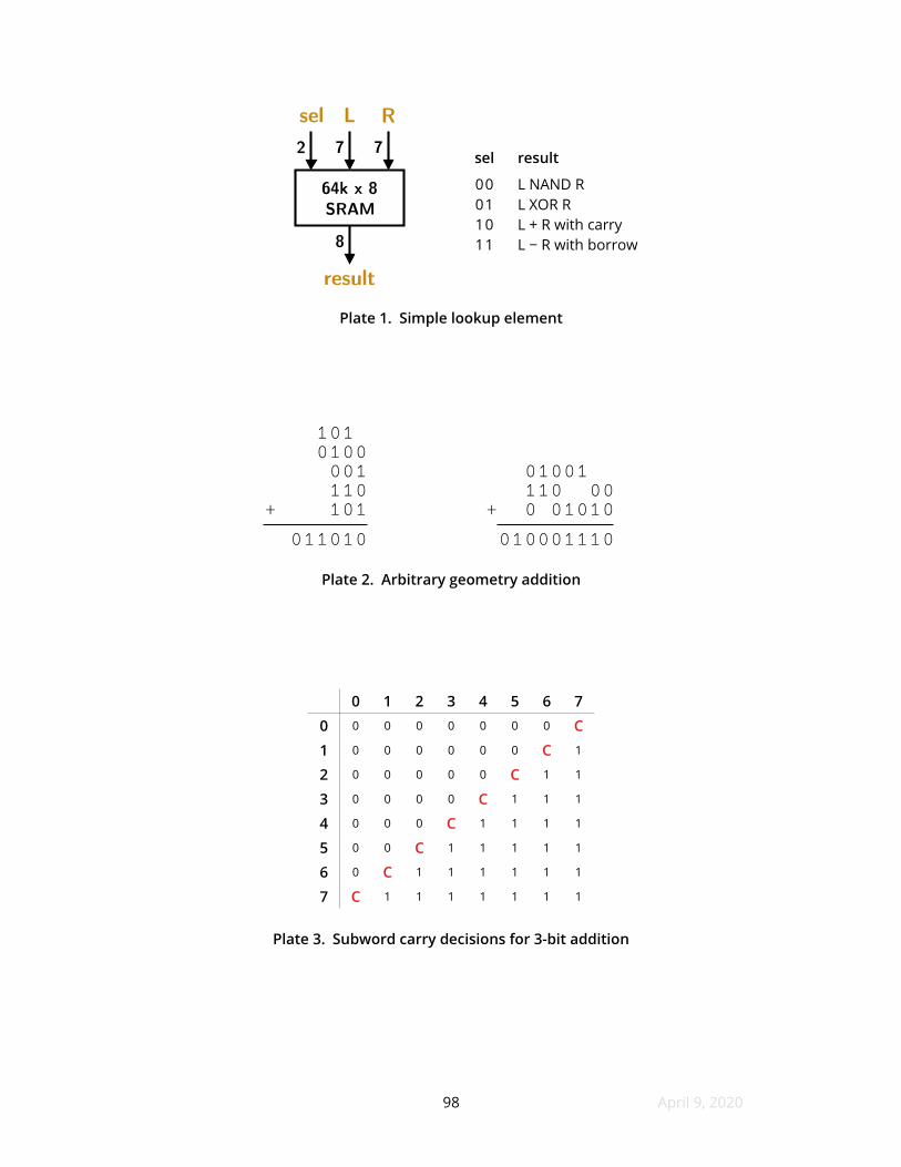
or two subwords and sometimes a carry bit Plate 1 shows an example with two
logical and two arithmetic functions Plate 2 show a another problem type that can
be solved using simple lookups
Two frequent design tradeofs arise when using simple lookup elements First
unary operations can ofer input widths of twice what binary operations can Second
the presence of a carry input tends to halve the number of operations a RAM can
provide for a specifc operand confguration
23 Arbitrary geometry adders
Arbitrary geometry adders are a special case of simple lookup elements Plate
2 shows two addition problems with more than two addends and irregular column
27 April 9 2020
spacing In the right example therersquos either a bit missing within an addend or a line
with more than one addend depending on interpretation Both examples share a
non-obvious feature of exactly 16 input bits because each is a one-RAM subtask
from the binary multiplication demonstration in Section 29 There is nothing tricky
just tedious about how these two RAMs are programmed some kind person
computes all 216 possibilities using the place values shown
Simple RAM lookup elements are all over the computing literature and
especially prevalent in PLDs and FPGAs The case of arbitrary geometry adders using
SRAM isnrsquot in widespread use or discussion known to me but relates to and
conceptually derives from the full- and half-adders used in Wallace [17] and Dadda
[18] multiplier circuits since the mid-1960s
24 Carry-skip adders
Carry-skip adders combine subwords by augmenting not-always-certain carry
outputs with a propagate output that is set whenever the correct carry output is
indicated by the carry output from the immediate right subword Plate 3 shows the
carry outputs that will occur when two 3-bit subwords are added with a possible
carry input In practice we add wider subwords but this size keeps the illustration
legible The key concept is that at times the carry output cannot be computed until
the carry input is known and when this occurs the carry output is always exactly the
carry input So if two machine words are added by means of parallel subword
additions subword place value results must be determined later than subword carry
results The circuit responsible for this is called a carry-skip adder and a 12-bit
example combining 3-bit subword additions appears as Plate 4
As Plate 4 shows the number of stages to consider increases as we move
leftward this is like a spatial transposition of the time sequence of ripple-carry
adders Traditional carry-skip adders have a time-sequential propagation of carry
information from right to left but they move by subwords and therefore ofer a
speed beneft over ripple-carry adders SRAM carry-skip adders go a step further
28 April 9 2020
they donrsquot exhibit any right-to-left time behavior at all but instead use their table
lookup power to simultaneously make all carry decisions This is unique to table-
based carry-skip adders about which I have found no reports in the literature
SRAM carry-skip adders can be categorized into designs that use either two or
three gate delays A distinguishing characteristic of 2-layer adders as pictured in
Plates 4ndash6 is that their carry deciding and fnal subword incrementing happen
simultaneously They donrsquot determine the carry decision and then apply it nor even
compute the needed carry decision at all They merely apply the correct carry
decision as if it had been computed Here the magic of table-driven computation
removes a stage
Although SRAM carry-skip adders are always ripple-free and sometimes skip
intermediate carry decisions as well this doesnrsquot make them universally faster than
familiar carry-skip adders Their zillion transistors of RAM are far slower than
directly-constructed single-purpose logic like a word adder So SRAM isnrsquot going to
revolutionize microprocessor8 addition circuits What SRAM can do is build
reasonably fast adders for supremely secured and assured systems
Numerous tradeofs and alternatives appear in SRAM carry-skip adder designs
Plate 5 moves the old carry input to the frst layer saving much address space and a
RAM in layer two but crowding the least-signifcant layer one RAM more This change
also reduces potential to reuse this circuit for purposes other than additionmdashrecall
that these devices are merely RAMs and they only become adders because of their
contents In fact potential uses other than addition sometimes require that carry
information propagate not from right to left as for addition but from left to right9
Plate 6 shows a ldquobidirectionalrdquo carry-skip adder that can propagate information
in either direction Note the choice to introduce the old carry at the second layer
and which SRAM the new carry is deemed to appear at depends on the direction of
operation Although bidirectional operation consumes more inputs at layer 2 their
use fattens out among the RAMs and is in one respect a simplifcation Although this
8 A microprocessor is a die that contains at least one complete CPU9 Left-to-right examples include NUDGE (see Section 47) and count leading ones
29 April 9 2020
circuit appears to be useful due to its directional fexibility an ALU that supports the
bit reversal permutation can mirror bits with a preliminary instruction do the
intended operation with ordinary right-to-left carries and if need be mirror back the
resulting bits Considering the scarcity of occasions that a left-to-right carry is
needed using bit reversals insteadmdashprovided they are fastmdashmight be a better
design for some ALUs
Plate 7 ofers a remedy for the crowded propagate and carry wiring associated
with 2-layer carry-skip adders It isnrsquot the wiring of course but the address space
memory and transistor count for the high-place-value subwords which need
conservation Two ends of a candle are burning First the available subword size for
computation soon reaches zero in the bottom layer which the top layer must also
mirror This sets an upper limit on the total word size that can be added Second the
adders in Plates 4ndash6 only add due to the absence of input bits to select other
operations We need to fnd more address bits
Plate 7 adds a middle layer to our carry-skip adder Only one SRAM is needed
for this layer because it doesnrsquot touch any of the tentative sums It simply reckons
the propagate and carry subword outputs into carry decisions that are passed to
layer 3 The last layer of SRAM is much cleaner with each RAM requiring only its own
carry decision alongside its tentative sum The conserved address bits can be used
for other purposes notably function selection and perhaps another operand if a use
for one emerges
Switching to a 3-layer adder adds 50 to its propagation delay a cost that
requires justifcation This extra delay isnrsquot as harsh as it might sound because
additional delay exists in the datapath The CPUrsquos clock will lose at most 20 due to
adding this third layer subject to a few assumptions As for justifcation here are
three items First a lot of address space opens up in the third layer enabling other
computation by these RAMs for non-additive instructions Second a lot of time
opens up in the second layer because Plate 7 has nothing happening to the tentative
sums as the carries are being decided The second layer can be flled in with more
RAMs to do more computation with no further performance penalty Third the high
30 April 9 2020
fan-out in 2-layer adders for propagate and carry signals incurs a speed penalty
One of the limitations of the adder circuits wersquove considered is their bandwidth
limitation when computing across subwords At best the frst layer can broadcast at
most two bits per subword to the other subwords and the three-layer adder can
receive at most one bit from other subwords in the third layer It would be helpful if
we can route a lot of wires between subwords instead of within them particularly if
we can fgure out a good system for using the extra connectivity
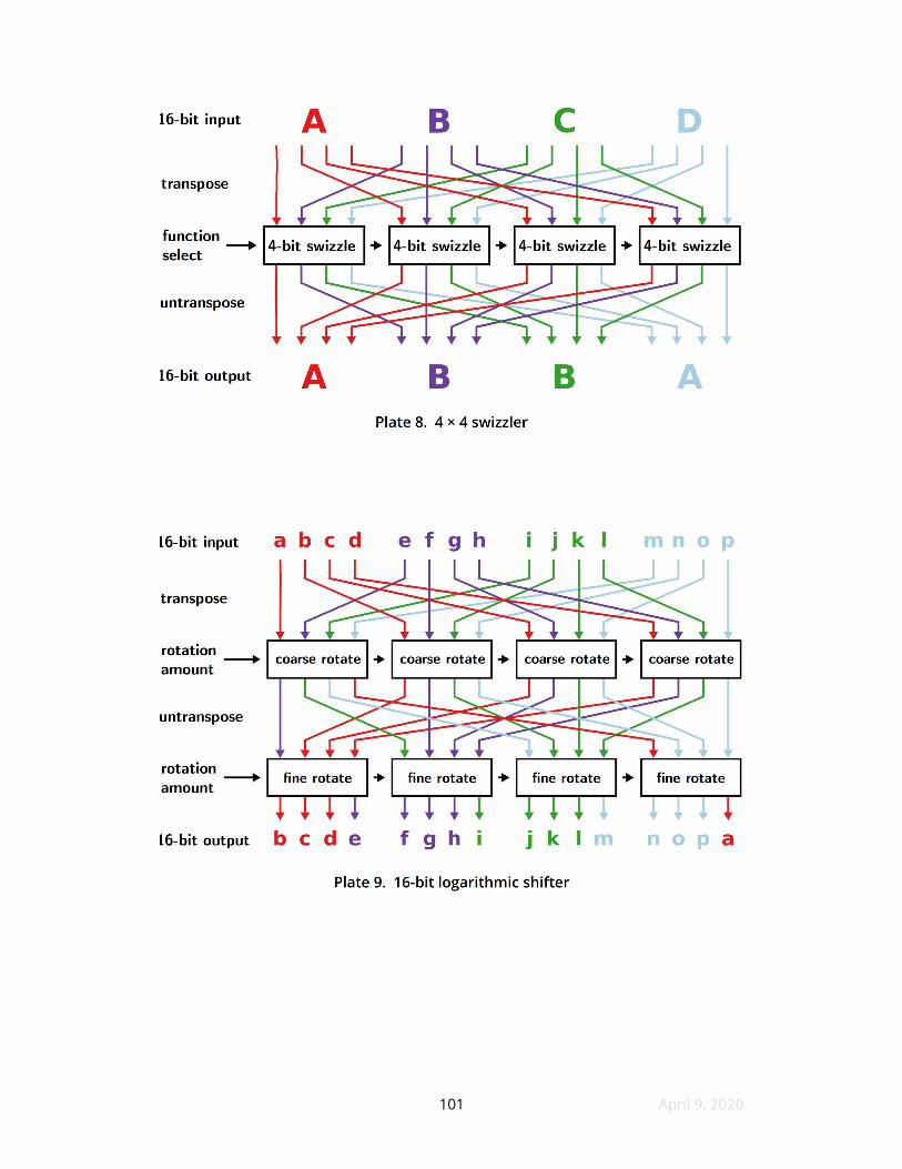
25 Swizzlers
A swizzler is a layer of RAMs that operate on transposed subwords meaning
that each RAM gets one address bit from each subword looks something up and
returns one bit to each subword Plate 8 shows how this transposition is wired for a
16-bit word with 4-bit subwords From right to left each of the four RAMs operates
solely on place value 1 2 4 or 8 If the four RAMs have the same contents and same
function chosen subwords will be treated as atomic entities This is the case in the
illustration the operation here is copying the leftmost subword to the rightmost and
copying the inner left subword to the inner right The four letters may be interpreted
as either literal hexadecimal digits or 4-bit variables
Some magic needs to happen in terms of advance planning because the
number of functions these RAMs can hold (and therefore execute) is a tiny sliver of
the number of functions possible Additionally we need to consider that the RAMs
might require unequal contents to achieve certain objectives Itrsquos also possible that
the function select bits applied might not be the same across all of the RAMs Itrsquos
even possible that there isnrsquot an input bit that corresponds directly to each output
bit some outputs might be fxed ones zeros or some function of multiple inputs It
turns out that all three of these ldquomightsrdquo turn out to be very advantageous although
none are suggested by Plate 8
31 April 9 2020
26 Logarithmic shifters
A logarithmic shifter overcomes a key limitation of swizzlers which are perfect
for fast rotation of subwords but not of bits If we assign one bit each to letters andashp
we can swizzle mnop abcd efgh ijkl to become abcd efgh ijkl mnop But when
we try to rotate just one bit position from here instead of four the result will be
ebcd ifgh mjkl anop because place values remain fxed In fact only the leftmost
RAM would move anything because the remaining transposed subwords are already
correct To fnish our one-bit rotation we have to clean up the subwords individually
to yield bcde fghi jklm nopa which is what we want This requires a second layer
of RAM that can operate within subwords rather than across them Plate 9 shows
this combination which permits rotation of any number of bits in a single pass
Masking is easily added to the values in the RAMs to supply left and right shifts of
any number of bits
Three important properties pertain to logarithmic shifters First sign extension
works out to support right arithmetic shifts every RAM that needs a copy of the
leftmost bit will receive it in time Second the RAMs within a layer need to all process
the same number of bits Third the bits leaving the RAMs of layer one must be
evenly distributed to the RAMs of layer two Thus when the two layers do use the
same number of RAMs the subword size will be a multiple of the number of
subwords Equivalently the word size will be a multiple of the square of the number
of subwords
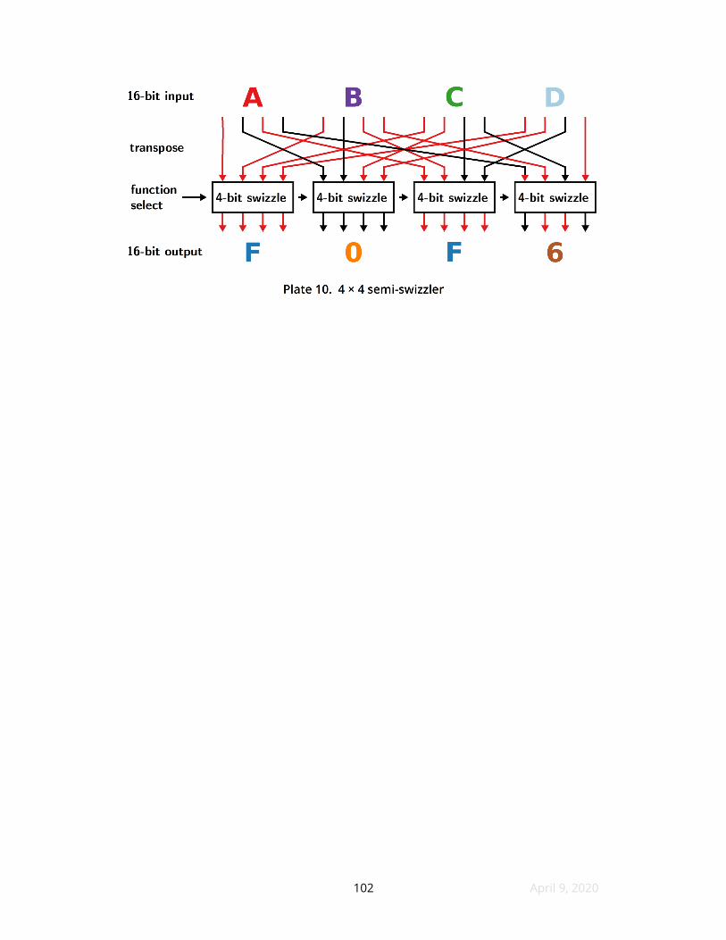
27 Semi-swizzlers
A semi-swizzler or half-shifter is a contiguous half of a logarithmic shifter that
is a transposition preceding or following a layer of swizzle RAMs but no
transposition going the other direction An example appears at Plate 10 using the
same input data and SRAM contents as Plate 8 The computed output looks like
gibberish because it is still transposed A semi-swizzler can be applied twice by a
program using two consecutive instructions to achieve ordinary shifts and
32 April 9 2020
rotations Section 3 discusses the mechanism and tradeofs of superposing a 2-layer
adder with a semi-swizzler to build a compact ALU
Because the RAMs of a semi-swizzler comprise both the frst and second layer
of a logarithmic shifter the CPU word size must be a multiple of the square of the
number of RAMs in the semi-swizzler
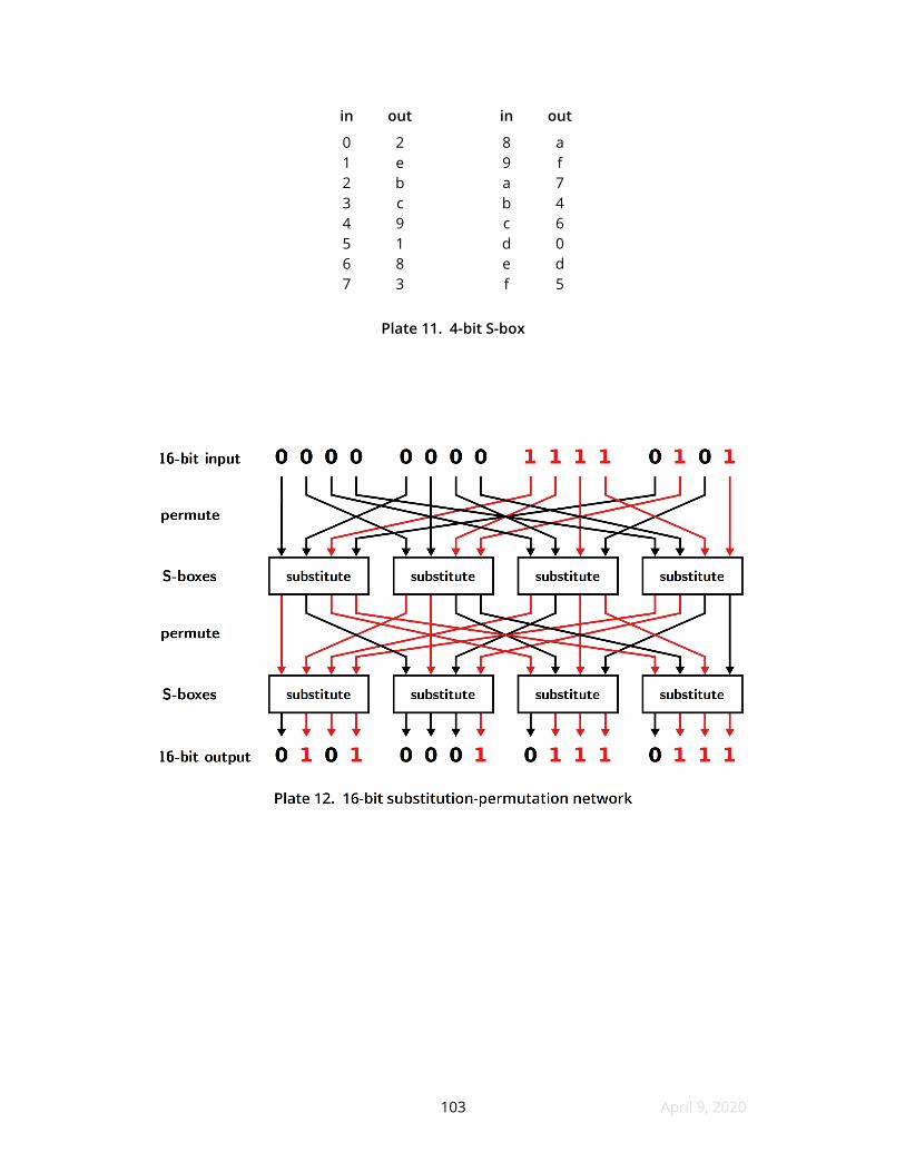
28 Substitution-permutation networks
An S-box is an invertible substitution that can operate on subwords Its
purpose is to help progressively alter words in a key-dependent manner until the
alteration sequence is impractical to reverse without knowledge of the key that was
used Plate 11 shows a simple 4-bit S-box expressed in hex Due to our requirement
for invertibility no value appears more than once in an S-box or its inverse
A logarithmic shifter with its SRAM contents replaced by S-boxes is an instance
of a substitution-permutation network or SPN Its intent is to scramble and
unscramble bits by mixing data as it passes through layers of cross-connected
S-boxes SPNs are used for constructing hash functions pseudorandom number
generators and ciphers Desirable topologies for SPNs as well as properties of
cryptographically ldquostrongrdquo S-boxes have been topics of secret research for half a
century Plate 12 shows a small SPN built using the S-box of Plate 11
There is nothing novel about SRAM SPNs but their mixing capability is very
useful for ALUs to incorporate They are best used under non-adversarial
circumstances eg to implement hash functions and PRNGs Suitability for
cryptography is considered in Section 49
29 Fast multipliers
Fast SRAM multipliers are nearly as fast as adders in practice however the
number of RAMs needed grows a little faster than the square of the word size The
process itself is primarily one of summing partial products quickly As schematics of
multipliers are tedious to draw and not particularly legible here is a walkthrough of
33 April 9 2020
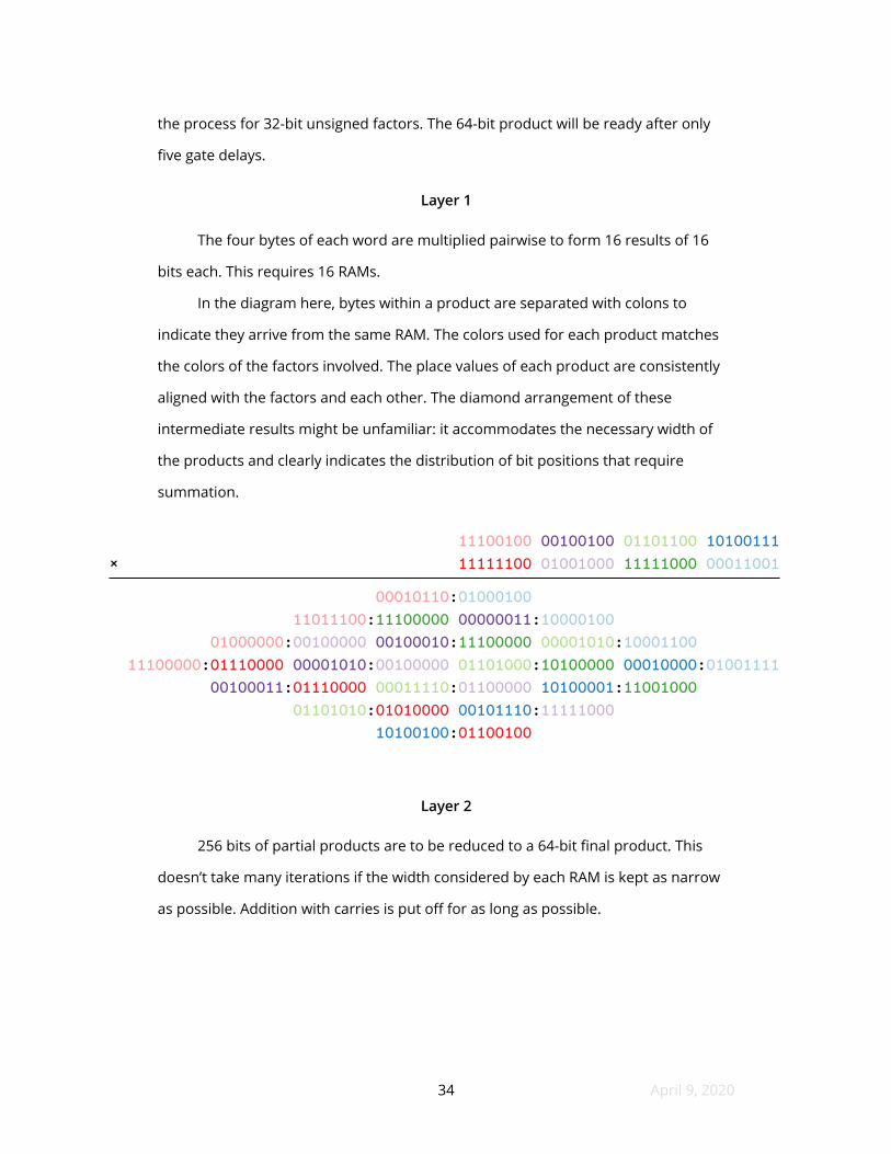
the process for 32-bit unsigned factors The 64-bit product will be ready after only
fve gate delays
Layer 1
The four bytes of each word are multiplied pairwise to form 16 results of 16
bits each This requires 16 RAMs
In the diagram here bytes within a product are separated with colons to
indicate they arrive from the same RAM The colors used for each product matches
the colors of the factors involved The place values of each product are consistently
aligned with the factors and each other The diamond arrangement of these
intermediate results might be unfamiliar it accommodates the necessary width of
the products and clearly indicates the distribution of bit positions that require
summation
Layer 2
256 bits of partial products are to be reduced to a 64-bit fnal product This
doesnrsquot take many iterations if the width considered by each RAM is kept as narrow
as possible Addition with carries is put of for as long as possible
34 April 9 2020
11100100 00100100 01101100 10100111times 11111100 01001000 11111000 00011001
0001011001000100 1101110011100000 0000001110000100 0100000000100000 0010001011100000 0000101010001100 1110000001110000 0000101000100000 0110100010100000 0001000001001111 0010001101110000 0001111001100000 1010000111001000 0110101001010000 0010111011111000 1010010001100100
In this picture the bits above the line are an exact repetition of the previous
layerrsquos output but their colors now indicate which RAMs they are grouped into for
addition The rightmost place value of each color group can be observed to be the
same before and after this operation Each band can group as many as 16 input bits
The process used is the arbitrary geometry addition from Section 23 and is a simple
table lookup The black digits on the left and right are not being added but are
passed forward for later addition (left) or for direct use in the fnal product (right)
The reduction in bits is considerably faster than one fnds in Wallace [17] or Dadda
[18] multipliers because the SRAMs ofer fuller capability than full- and half-adders
As this step starts 8 bits are fnished and 248 remain to add Afterward 13 bits are
fnished and only 99 remain to add 15 RAMs are used
Layer 3
The process of layer 2 repeats with 6 RAMs and further gains
35 April 9 2020
00010110 01000100 11011100 11100000 00000011 10000100 01000000 00100000 00100010 11100000 00001010 10001100 11100000 01110000 00001010 00100000 01101000 10100000 00010000 01001111 00100011 01110000 00011110 01100000 10100001 11001000 01101010 01010000 00101110 11111000 + 10100100 01100100
00100 00 001 101 0010 11 01001 0100 010 11100000 010000 001000 000110 0001010 0100100 01001111 00 110100 0 11010 0 10011 01 1010 010 1011
00100 00 001 101 0010 11 01001 0100 010 11100000 010000 001000 000110 0001010 0100100 01001111 + 00 110100 0 11010 0 10011 01 1010 010 1011
1110 00 1110000 00100 011 1001000 01100100 01001111 00000 1101010 010 01001 0100011 10
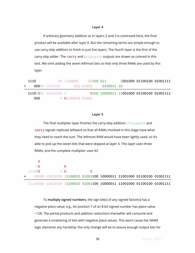
Layer 4
If arbitrary geometry addition as in layers 2 and 3 is continued here the fnal
product will be available after layer 6 But the remaining terms are simple enough to
use carry-skip addition to fnish in just fve layers The fourth layer is the frst of the
carry-skip adder The carry and propagate outputs are drawn as colored in this
text We omit adding the seven leftmost bits so that only three RAMs are used by this
layer
Layer 5
The fnal multiplier layer fnishes the carry-skip addition Propagate and
carry signals replicate leftward so that all RAMs involved in this stage have what
they need to reach the sum The leftmost RAM would have been lightly used so itrsquos
able to pick up the seven bits that were skipped at layer 4 This layer uses three
RAMs and the complete multiplier uses 43
To multiply signed numbers the sign bit(s) of any signed factor(s) has a
negative place value eg bit position 7 of an 8-bit signed number has place value
minus128 The partial products and addition reductions thereafter will consume and
generate a smattering of bits with negative place values This wonrsquot cause the SRAM
logic elements any hardship the only change will be to assure enough output bits for
36 April 9 2020
1110 00 1110000 00100 011 1001000 01100100 01001111 + 00000 1101010 010 01001 0100011 10
11100000 11010100 1 0100 10000011 11001000 01100100 01001111 000 0 01100010 01001
0 00 0 111000 0 0 0+ 00000 11010100 11100010 01001100 10000011 11001000 01100100 01001111
11100000 11010100 11100010 01001100 10000011 11001000 01100100 01001111
each RAM group inputs in the correct address widths and precompute its addition
table correctly
To multiply numbers with any signedness build a signed multiplier with an
extra bit position eg build a 33-bit multiplier for 32-bit words using the extra bits
in layer 1 as a signedness bit instead of as a sign bit This approach is better than
applying the grade-school ldquoa negative times a positiverdquo rule to the entire problem
Although conceptually simple the school method would either add many RAMs and
almost double the gate delay or use additional instructions for testing and
branching
The division of the original factors into subwords does not need to be
symmetric as long as all product and sum place values are grouped correctly For
example an any-signedness multiplier for 32 bits using 64kthinsptimesthinsp16 SRAMs does not
need to spill from 16 partial products into 25 in order to ft the signedness bits One
factor can have four subwords of [7 bits + signedness 8 bits 8 bits 9 bits] and the
other fve subwords of [5 bits + signedness 6 bits 7 bits 7 bits 7 bits] for 20 partial
products calculated by 20 SRAMs10 I have not counted the number of subsequent
layers needed or the number of RAMs in each layer as the work proposed will
provide a tool to do so quickly Another confguration would be to maintain 16
devices in layer 1 by enlarging some of the RAMs This confguration adds 9 Mibit to
layer 1 with unknown changes to the memory used by the other layers Automating
the design process will make it easy to identify multiplier confgurations with the
fewest gate delays and least cost
10 This confguration could use mainly 32kthinsptimesthinsp16 and 16kthinsptimesthinsp16 RAMs but the former sell for more money than 64kthinsptimesthinsp16 and the latter arenrsquot ofered for sale There is at least a slight reliability beneft in leaving much of a 64kthinsptimesthinsp16 RAM unused as the opportunity for soft errors is proportionately reduced There may also be some energy saved depending on the cell design of the chips selected
37 April 9 2020
3 2-LAeER ALU DESIGNS
31 An elegant 2-layer ALU for 36-bit words
A standard 64kthinsptimesthinsp16 RAM is functionally a dual byte-wide device with shared
address inputs The two output bytes have separate enable lines and can be
independently put into a high-impedance state We can leverage this to build ALUs
with very few components by superposing a semi-swizzler onto the frst layer of a
carry-skip adder
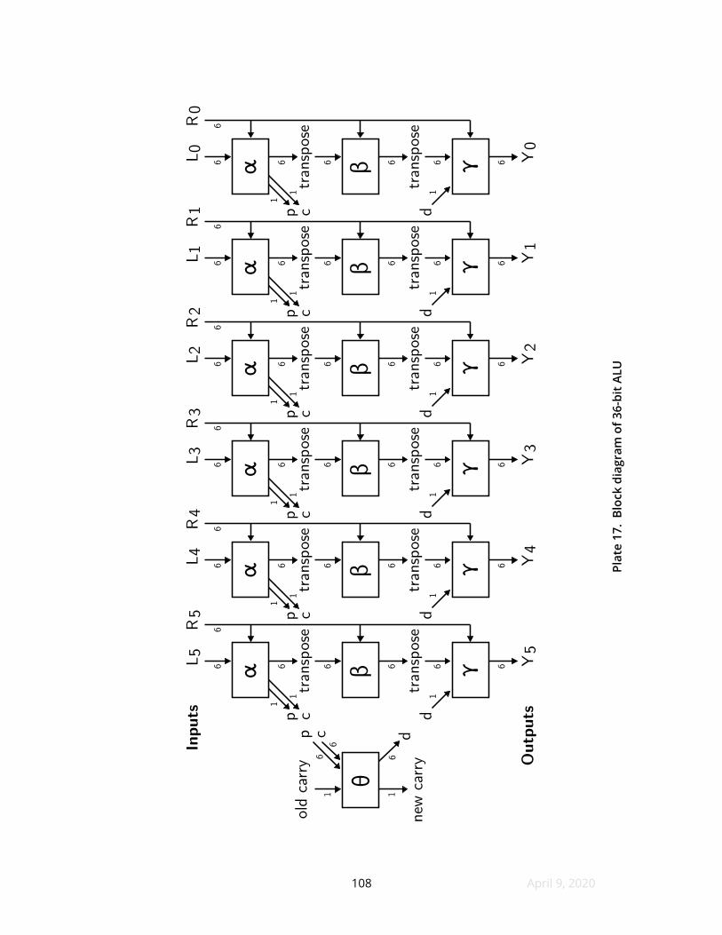
Plate 13 shows a 36-bit ALU made from just ten RAMs in two layers These
RAMs operate on 6-bit subwords to do all the work and this illustration only shows
the wiring for the subwords themselves The various control signals are drawn
separately for legibility as Plate 14 but note that the ten boxes refer to the same ten
RAMs in both fgures
The top layer of the ALU does almost all the work 16 functions accepting two
inputs of six bits are stored in the upper bytes of the top-layer RAMs The functions
are selected via a 4-bit control input (Plate 14) and the byte select lines (not shown)
enable the upper bytes while forcing the lower bytes to high impedance This mode
provides a traditional mix of additive and logical functions as well as subword
multiplications There is no hardware support for 36-bit times 36-bit multiplication
By enabling the lower bytes of the top-layer RAMs and forcing the upper bytes
to high impedance the outputs are transposed in the manner of a semi-swizzler
These lower bytes provide 16 functions for swizzling rotations shifts permutations
S-boxes and other operations that beneft from transposition The performance
penalty is that the transposition only goes in one direction per instruction executed
so in nearly all cases it takes two CPU instructions to do anything with these lower
bytes
A second factor derates the speed of this ALU the fan-out for propagate and
carry signals peaks at seven including startup hardware and a yet-unmentioned
overrange output This speed penalty is small enough that bufering would make the
38 April 9 2020
delay worse yet large enough to increase the appeal of a three-layer design
The bottom layer does nothing other than add whatever carries are required
during addition and subtraction All other functions including the lower byte
functions with transposed outputs must force their propagate and carry outputs low
so that the bottom layer does not spuriously change results Also although the
bottom layer conceptually has fve RAMs the carry decision task for subwords e1 and
e2 takes so few inputs that one RAM can settle both subwords
This ALU does not quite fnish all calculations in two layers Because the
subword outputs are not known until the bottom layer has fnished processing a
zero fag is not yet computed for the whole 36-bit result For this reason fve
subword zero signals are shown emerging from the ALU An external fve-input
NAND gate combines these signals into an aggregate zero fag There will be enough
surrounding delay in the datapath to absorb the NAND gatersquos delay
The RAM on the bottom left has one more address line than the others to
accommodate a carry output This is a 2 Mibit 128kthinsptimesthinsp16 device The remaining RAMs
are 64kthinsptimesthinsp16 This ALU has no carry input because all address lines on the top right
RAM are tasked for other uses As the word size is already 36 bits an occasional
branch on the carry fagrsquos value is typically enough support for adding and
subtracting wider integers
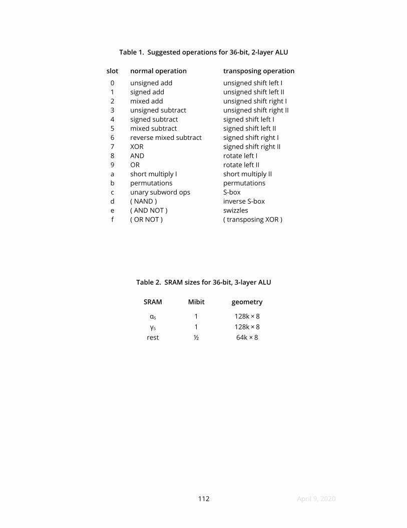
Table 1 maps out space in the frst RAM layer for suggested operations of this
ALU This tablersquos purpose is to show (i) an appropriate set of operations to
implement and (ii) that the complete set can be implemented within the address
space available Several provisions made in this table arenrsquot immediately obvious so
here is some explanation
This ALU always produces a 37-bit signed result when adding or subtracting
irrespective of operand signedness but the 2minus36 bit inaccurately termed the ldquosign
bitrdquo does not ft within a word and is not retained after the result is inspected for
overfow The inspection is fairly simple If the 2minus36 bit does not match the 235 bit and
the result is signed overfow will occur upon truncation If the result is unsigned and
the 2minus36 bit is set overfow has already occurred Overfow will not occur If neither
39 April 9 2020
situation applies For signed results the 235 bit then becomes known as the 2minus35 bit
All this would work out fne with 37-bit signed inputs but what come from the
registers are the customary 36-bit overloaded-signedness inputs Our workaround is
to have separate ALU operations for the several operand type combinations this is
why Table 1 requires three add and four subtract operations The surrounding CPU
will test for wrap-around and latch a Range fag when needed
There arenrsquot obvious identity clear or bitwise NOT operations for this ALU but
all three can by synthesized from XOR and constants Short multiplication works
across matching subwords and is always unsigned Two cycles are needed because
six 12-bit results are produced The low-order subwords are produced by the normal
operation The high-order subwords appear in the same place values as their
operands because thatrsquos where the RAMs are This means that prior to adding
subwords of a product together the high subwords must be shifted six bits left In
anticipation of this the high subword multiplication operation supplies the initial
transposition for the shift reducing by one the number of cycles needed
The reader might wonder how overfow is avoided for short multiplication as
the result is potentially 42 bits Usually nothing needs to happen because the main
use for short multiplication is to compute memory addresses of array elements Itrsquos
reasonable to expect the main memory to be SRAM not DRAM For a multiplication
result to exceed 36 bits at 2020 prices more than $400000 in SRAM needs to be in
the system
Permutations swizzles and S-box operations usually require word
transposition and are specifed accordingly Plain permutations within subwords also
are supported A set of 64 unary operations selectable at the subword level are
included One of these operations computes the fxed-point reciprocal
lfloorthinsp(236 minus 1) divide max(n 1)thinsprfloor the largest unsigned word one can multiply by n without
overfow Most of the remaining 63 are simpler a starting list of candidate
operations appears as Table 21
Shifts are rotations are implemented in two CPU cycles because these require
two permutation stages and two transpositions The number of positions to move by
40 April 9 2020
must be replicated beforehand into each subword Thus a rotation may take four
cycles if the number of positions cannot be expressed as a constant two to
transpose replicate and transpose back the rotation amount and two to accomplish
the rotation itself Negative shifts and rotations are unavailable because the range
minus35 hellip +35 cannot be expressed within a 6-bit subword As right rotations are
expressible as left rotations separate functions for right rotation are not helpful
When rotating right by a variable amount no subtraction from 36 is required prior to
replication into subwords because one of the 64 available swizzle operations can
combine the needed subtraction and permutation No speed is lost by leaving out
right rotation
Plate 14 purposely omits some control logic that would easily confuse readers
who are trying to understand this ALU for the frst time In addition to what is drawn
the propagate signals from the fve RAMs which ofer them are combined in a fve-
input NAND gate The output of that gate is used only for left shifts and indicates
that signed or unsigned overfow resulted from a multiplication by a power of two
There are more subtleties The rightmost RAM doesnrsquot have an output bit left for
overfow detection it got used for zero detection Here we are helped by a kludge
Cycle two of a left shift operates on transposed words meaning that fve of the six
bits not checked during cycle one can be tested by other RAMs on cycle two This
leaves only the 20 bit not tested a bit which can only overfow during shifts of more
than 34 or 35 bit positions depending on signedness Smaller fxed shifts neednrsquot
check the 20 bit at all Of the remaining cases the only shift amounts that can
overfow always do when shifting a nonzero word11 The few programs that canrsquot be
written to preclude all possibility of such unorthodox shifts must assume
responsibility for checking the 20 bit But for most software this ALU detects left shift
overfow as perfectly as it detects additive wrap-around Masking for left shift canrsquot
happen until cycle two or overfow from the rightmost subword will go undetected
The overrange conditions for addition subtraction and left shift are not
11 The surrounding instruction set implements logical left shifts as unsigned left shifts with the overfow signal suppressed This is the ordinary case when the rightmost bit might shift more than 35 positions
41 April 9 2020
routine events comparable with the carry fag that other ALUs set These conditions
almost always involve processing errors meaning that the indicating fag must only
be cleared by an opcode exclusive to that purpose A latching fag precludes the
need to check after every arithmetic operation whether or not something bad
happened Instead a long sequence of perhaps thousands of instructions can be
run followed by a single fag check prior to committing the result to a database or
other observable outcome
The parenthesized operations in Table 1 are useful but non-essential and
subject to displacement for good cause
This ALU is not the most capable one a user can build on her own for high-
confdence applications but it already towers over the prior art For uses where its
speed and operations are suitable anyone with the motivation can build or have
built a practical robust inspectable and tamper-evident ALU for 36 bits using ten
small fungible RAMs I believe that on for the total component count as well as the
limited availability of parts that might be regarded as trustworthy it would be
difcult to improve on the overall design of this ALU This device is conceptually
mature and the design frontier has moved to the CPU which surrounds it
32 A tiny ALU for 18-bit words
The ALU of Plates 13 and 14 canrsquot be cut down to build a 24-bit or 30-bit
version because 24 and 30 are not multiples of 16 and 25 (the squares of the
number of subwords in the semi-swizzler) respectively This means we cannot meet
the requirement to have a self-inverse transposition and a single subword size at the
same time But we can build 12- and 18-bit versions and these ALUs require only
three or four RAMs respectively The transpose wiring shown for 18 bits on Plate 15
is rearranged to minimize loss of left shift overfow detection Only the 20 and 21 bits
are unchecked so arithmetic shifts of up to 15 bit signed and 16 bits unsigned come
with range checking The right half of Plate 14 shows the control signals where the
worst fan-out (including two sinks not shown) is fve The instruction set can be as
42 April 9 2020
stated in Table 1 although the S-box outcomes will not agree with the results of their
36-bit counterparts
43 April 9 2020
4 3-LAeER ALU DESIGNS
41 An elegant 3-layer ALU for 36-bit words
A three-layer carry-skip adderrsquos middle layer is substantially empty because
the only thing happening is tabulation of carry decisions By placing a swizzler in the
middle layerrsquos datapath and overlaying a logarithmic shifter with the adderrsquos frst
and third layers we can build a robust ALU using 19 RAMs Plate 16 shows this
superposition Several improvements over the two-layer design arise at the cost of
some additional hardware and approximately 15 added to the cycle time12
Plates 17 and 18 show the general arrangement of a 3-layer 36-bit ALU with
the latter plate showing how the bit slices are assembled For clarity of reading the
transposition wiring across subwords is not drawn but is identical to the lower-byte
transposition on Plate 13 As the transposition is self-inverse and happens both
before and after the middle layer the outer layers see no transposition when the
middle RAMs act transparently The layers implement so many functions that they
defy naming so they are named α β and γ after their order of appearance Their
RAMs are numbered 0ndash5 from the right so the notation α5 designates the most-
signifcant RAM of the frst layer The carry decision RAM one in number is
denoted θ
17 bits from the instruction decoder tell the ALUrsquos RAMs what function to
implement of which 14 are visible on Plate 1813 These separate layer controls plus
additional control for θrsquos carry decision method can get a lot of work accomplished
in one pass The right operand is fed to all three layers unmodifed allowing any
layer to either compute a function of two inputs or select any of 64 single-input
functions on a per-subword basis
This ALU has 105 Mibit of SRAM in 19 packages Table 2 lists their individual
sizes As these byte-wide RAMs are not sold today actual device widths will be 16
12 The cycle time penalty is estimated using fve total datapath layers for the 2-layer ALU 10 ns SRAM access time 2 ns per layer delay for board capacitance and a 3 ns fan-out penalty for the 2-layer circuit The 3-layer ALU adds a net 9 ns to the datapath
13 Section 411 accounts for the three control bits not shown
44 April 9 2020
bits and total physical storage will be 21 Mibit Itrsquos possible to ldquofoldrdquo the 64kthinsptimesthinsp16 size
into 128kthinsptimesthinsp8 units at the cost of some capacitive load and added inverters thereby
removing dependency on having the 128k size available for two of the RAMs There
is no advantage folding 32kthinsptimesthinsp16 into 64kthinsptimesthinsp8 as 32k is scarce and more expensive
The total cost for all the RAM is around US $30 in 2020
Our term for a 6-bit subword is tribble as itrsquos a multiple of three bits This is
analogous to a byte in power-of-two word size architectures Unfortunately tribbles
are not wide enough to encode even US ASCII which requires only seven bits
however Unicode has greatly eroded the usefulness of bytes for symbol
representation anyway
Tables 3 and 4 show input and output bit assignments for all of the RAMs and
appear mainly as assurance that enough wires exist on the packages They donrsquot
require study for one to understand the ALU in general terms
Table 5 summarizes opcodes this ALU implements by category Many opcodes
donrsquot appear in this list because their naming semantics for the assembler have yet
to be decided14 Tables 6ndash13 show the mechanisms that implement the named
opcodes The general format frst lists the assembler mnemonic on the left A given
mnemonic can generate several diferent opcodes depending on the signedness of
its arguments and results For example the mnemonic A (add) in Table 6 includes
overfow checking that requires awareness of the signedness of both arguments and
the result and this awareness is supplied by using eight diferent opcodes for A This
multiplicity is indicated in the second column The next four columns indicate the
function select inputs for the three ALU layers and carry decision RAM To keep the
tables compact and legible these SRAM operations have single-character names
and are described in further detail in Tables 14ndash19 The next column shows what
must be supplied as the right operand by default this column simply reads ldquoRrdquo
meaning the natural right argument of the intended operation is supplied
14 For example there is no mnemonic yet for reversing the bits of a word although the capability is present via a stacked unary operation
45 April 9 2020
42 Additive opcodes
Table 6 shows the basic addition and subtraction opcodes The α and γ layers
provide carry-skip addition with β not participating An extra subtract operation is
ofered with the arguments reversed a special provision for CPUs with fast hardware
multipliers15 Subject to whether or not rdquowith carryldquo is specifed in the opcode θ
distributes correct carry decisions to γ The INC DEC and NEG assembler
mnemonics donrsquot correspond to actual opcodes but conveniently provide right
arguments for add subtract and reverse subtract This is why these mnemonics
show zero for their number of opcodes
Addition and subtraction are stratifed by signedness causing six mnemonics
to assemble to 48 distinct opcodes depending on the signedness of the arguments
and result This permits not only mixed-sign arithmetic eg add a signed register to
an unsigned register but also alerts the CPU as to the signedness of the destination
register so that overfow is detected correctly Section 411 ofers more specifcs as
to how these checks work
43 Bitwise boolean opcodes
There exist sixteen bitwise boolean functions with two inputs and as Table 7
shows this ALU implements all of them Interestingly the individual layers only
implement a handful of these α supplies the common AND and OR operations β is
very limited in its fexibility to assist because itrsquos operating on a transposed word
The only change it can safely make is to invert all bits thereby extending what α can
do to include NL NAND and NOR γ doesnrsquot have enough space to ofer many
operations because its carry input cuts in half the available space for their
implementation But by XORing what arrives from β with the original right operand γ
adds another fve operations γrsquos multiplex and kill operations manage to fll out the
remaining constants and identities
15 The ALUrsquos arguments come from two copies of the register fle which ordinarily have the same contents The 72-bit result from multiplication gets split between these copies causing that registerrsquos value to depend on whether it is the left or right operand of a subsequent subtraction
46 April 9 2020
Although the opcodes of Table 7 technically implement the boolean functions
listed not all do so semantically For instance the boolean function NR (ldquonot Rrdquo or
bitwise invert) function theoretically ignores its left input but this ALU cannot both
ignore its left input and invert its right input due to SRAM space limits Instead the
assembler has to substitute all ones in place of the left input register specifed in the
source code This doesnrsquot present a problem for users compilers or assembly
language programmers but it compromises style a tiny bit
44 Compare opcodes
In Table 8 we fnd opcodes for compare and shift tasks The maximum and
minimum operations are unusual in CPUs traditionally a compare and branch is
used but we accomplish these in one cycle Not only this but the two operands and
results can be of any signedness MAX and MIN are implemented by having α and β
pass the left argument unchanged and γ select between the output of β and the
right operand depending on whether the carry decision bits are all ones or all zeros
θ is able to compute which argument is larger on the basis of tribble comparisons
made by the α RAMs and delivered via the propagate and carry wires
The BOUND operation is intended for array subscripts Although BOUNDrsquos
implementation is the same as for ordinary subtraction separate opcodes are
counted for BOUND so that the link editor can locate and optionally remove array
boundary checking Additionally BOUND does not write any result to a register The
index tested is supplied in the right operand which may be unsigned or signed but is
evaluated as if unsigned The left operand is the bound Hypothetically the bound is
always at least zero but signed bounds are permitted to be passed (thus two
opcodes) in order to accept whatever data type the register is declared to be The
operation performed is simply subtraction the 2minus36 bit will be set if the index is less
than zero or at least as large as the bound The logic that monitors this bit and
interrupts the CPU is external to the ALU BOUND will not work correctly for bounds
of 235 or higher because indices that high will be interpreted as less than zero and
47 April 9 2020
therefore not within bounds But there wonrsquot be enough memory for this problem to
appear16 BOUND will never set the overrange fag instead the CPU is interrupted
The CMP instruction does a simple comparison and is identical to subtraction
except the control unit skips the step where the result is written to a register It
likewise does not check to see if the diference fts in any particular format and will
never set the overrange fag
45 Shift and rotate opcodes
The shift operations in Table 9 have unconventional defnitions Arithmetic shift
means multiplication or division by a power of two rounding towards negative
infnity in the case of division In traditional forums arithmetic shift means that a
signed number is being shifted But itrsquos moot whether the number is unsigned or
unsigned what is important is whether the intent is to perform arithmetic and if this
is the intent the result must be tested for overrange irrespective of signedness A
shift in the absence of any intent to multiply or divide is called in this proposal a
logical shift Logical shifts are not tested for overfow because the bits involved do
not represent quantities
The logarithmic shifter is implemented by the β and γ layers The shift and
rotate operations require the number of bit positions to be encoded into every
tribble of the right argument The notation R means to suggest a vector with all
subwords having the same value These identical copies can be provided by the
compiler or assembler if the shift amount is fxed otherwise a stacked unary
operation (Table 22) is used to replicate the correct value into each tribble
The γ layerrsquos participation in the logarithmic shifter is expressed in terms of
leftward rotation only because RAM in that layer is very scarce This means that all
shift and rotation operations are normalized to a left perspective so to shift right
one position the argument supplied must indicate a left rotation of 35 positions The
stacked unary operations that prepare shift and rotate arguments account for this
16 Someone who can aford a 236-word SRAM data memory wonrsquot have a problem upgrading to a 64-bit 3-layer ALU using 221thinsptimesthinsp16 SRAMs whereupon BOUND will give correct results up to 263 minus 1
48 April 9 2020
There are four sub-cases (shift vs rotate 0minus35 bits vs 36+ bits) not elaborated on
here Rotations in excess of 63 bits require extra instructions for the modulo-36
division needed
Negative shift amounts arenrsquot directly supported by this ALU because a signed
tribble can only represent numbers in the range minus32 hellip +31 while the range of
shifting is at least minus35 hellip +35 If a variable shift amount might have either sign a
branch is required to straighten out matters
Range checking for left arithmetic shifts is done in the α layer which encodes
the signed and unsigned overfow result for each tribble onto the propagate and
carry wires Two of θrsquos output bits are the logical OR of its propagate and carry
inputs these outputs return to the control unit so that overrange can be fagged
46 Multiply opcodes
Although this ALU isnrsquot specifed with a hardware multiplier it has several
opcodes that signifcantly accelerate unsigned multiplication in software Table 10
shows the implementation for these For short multiplication the right operand
must be a factor in the range of 0 to 63 and replicated across all six tribbles ML and
MH multiply across the tribbles of the left and right operands MH throws in a left
shift to align with ML so the results can be directly added for the fnal product So if
a b c and t are unsigned registers 0 le b le 63 and a times b lt 236 we compute c = a times b
in four instructions
t = b copy 0 replicate tribble 0 of b across tc = a mh t short multiply high tribblet = a ml t short multiply low tribble replaces tc = c add t final product
Short multiplication when b is constant only needs three instructions because
the compiler or assembler will provide the initial replication
Short multiplication correctly detects the overrange condition in which case
the result is of little value and might best be considered undefned Section 410
49 April 9 2020
gives more particulars
Long multiplication can be emulated in software For 36-bit unsigned integers
with 72-bit results 53 cycles are needed Except that we might not have CPU
microcode that dispatches these instructions transparently this performance is not
far out of line from the Intel 80486 which required 18 cycles even to multiply by
zero and up to 42 cycles for larger numbers
Assembly code showing long multiplication appears in Listing 1 Two opcodes
not used for short multiplication include MHNS (ldquomultiply high no shiftrdquo) which
multiplies tribbles pairwise but without shifting the result 6 bits to the left and DSL
(ldquodouble shift leftrdquo) a which shifts the high tribble of the right operand into the low
tribble of the left operand We also see COPe which selects a tribble from the left
operand and replicates it six times
The COPe opcode is actually a general call to any of the swizzles of Table 25
where the frst six operations happen to copy the six tribbles by position So COPe
with a right operand outside the range of 0ndash5 probably isnrsquot a copy at all This opcode
may later be known by some other name but is presently named for clarity as to
how it is used in this proposal
47 Bit scan opcodes
Table 11 shows implementations for some scan and mix opcodes LEAD and
TRAIL can be used for operations such as count leading ones Herersquos how they work
Suppose we wish to count the leading ones on the word
111111 111111 111100 011100 111111 111111
and a unary function is available for α or γ that counts leading ones on a per-tribble
basis That function returns the tribbles [ 6 6 4 0 6 6 ] The LEAD operation scans
tribbles from left to right and clears every tribble after the frst that is less than 6
The expectation is that αrsquos count of leading ones starts from the left and continues to
be valid for as long as no zeros are encountered Once α sees a zero it can fnish that
tribblersquos count but further results to the right from α do not count So LEAD replaces
50 April 9 2020
[ 6 6 4 0 6 6 ] with [ 6 6 4 0 0 0 ] These six tribbles are then added together using the
most efcient operations on hand to yield the full count which is 16 leading ones
LEAD and TRAIL work because α has an operation that tests the tribbles of L
and R pairwise to see if the left tribble is lesser θ receives those results via the carry
wires and has left and right scan functions to turn on the carry decision bits for
tribbles left or right of the point where the bit count fell short After that γ has a
function that zeros any tribbles where the carry decision input is high
Efciently adding the tribbles of a word together is a challenge and involves
simultaneously applying various unary functions to diferent layers This need occurs
not just for leading and trailing counts but also determining the Hamming weight of
a word sometimes called population count or simply popcount which is a count of
the number of set bits in a word For example we might begin with
100000 011000 001110 110011 111110 111111
and use one of αrsquos unary operations to count ones returning [ 1 2 3 4 5 6 ]
But now we have to add the tribbles For this purpose α β and γ ofer 64 sets
of ldquostacked unaryrdquo functions listed in Table 22 that are selected by the right
argument One such set implements ldquoadd six sets of three bits to yield three sets of
four bitsrdquo meaning a bit count of [ 1 2 3 4 5 6 ] can be reduced in one cycle to the sum
[ 0 0 0 5 7 9 ] How might this work Two three-bit addends can ft in a single tribble
So αrsquos lookup table could shift the three leftmost tribbles three bits left β could
move the three most signifcant bits of the three leftmost tribbles into the same
positions in the three tribbles on the right γ could then look up the 4-bit sum for the
packed 3-bit addends on the three rightmost tribbles By a similar process the next
CPU instruction can reduce [ 0 0 0 5 7 9 ] to [ 0 0 0 0 11 10 ] by splitting the four bits of
the frst addend into the two unused bits of the two other tribbles But as things
stand right now the last addition will require two CPU instructions to shift the 11
addend right and complete the addition
Thus we can obtain Hamming weight with no loops in fve cycles count ones
reduce to three addends reduce to two addends shift and fnally add Counting
trailing zeros uses six cycles count trailing zeros for each tribble TRAIL reduce to
51 April 9 2020
three addends reduce to two addends shift and add
There is a faster way to count leading or trailing bits in just four cycles by
avoiding the summation of six terms It uses θ between α and γ to convert the word
input to a word with at most one bit setmdashthe bit where the trail endsmdashin the frst
cycle Cycles two and three use β to locate that bitrsquos tribble and ofset within the
tribble and the fourth cycle adds the coarse and fne bit positions to give the fnal
result There are a few subtleties and tricks and the method doesnrsquot work for fnding
Hamming weights Whether this approach matures into assigned opcodes like the
fate of LEAD and TRAIL is subject to available space and depend on the degree to
which other unary and stacked unary functions need to be included
The NUDGE opcode adjusts the rightmost portion of a word which could be a
pointer to conform to a supplied template This template consists of a start bit
indicating the number of bits to replace and the replacement bits themselves For
example 0111010 NUDGE 0010110 replaces the rightmost four bits to give the result
0110110 in one instruction Without NUDGE this process would require two
instructions and would happen as ( 0111010 AND 0001111 ) OR 0000110
NUDGE is useful in part because many languages align memory that is
allocated to a small power of two Reportedly GNU malloc always returns a pointer
aligned to a multiple of eight or on 64-bit machines sixteen To the extent a
developer is informed of the alignment and can rule out unexpected change fast
access to various members of a structure can be available from close-enough
pointers As an example a node for a binary tree might have this form in C
struct j struct j left struct j right struct j parent
If we wish to disconnect some node n from its parent we need to dereference
the parent member then examine the left and right felds on the parent to see which
52 April 9 2020
matches n and set the appropriate one to NULL Thatrsquos a lot of work If struct j is
aligned to a multiple of four and NUDGE is available there is a faster arrangement
struct j struct j left struct j right struct j parent
With this format we can NULL the dereferenced word within the parent
without investigating which child n used to be The difculty is that the parent
member is only useful for deletions because it doesnrsquot know where within the
parent node itrsquos pointing The NUDGE opcode eliminates this problem If this C
program can access the NUDGE opcode we can in one cycle locate any member of
the parent by nudging the parent pointerrsquos alignment within its known power of two
More generally we can compute the address of a structure member in one cycle
from the address of another membermdasheven if we havenrsquot kept track of which
member the address calculation will start from
NUDGE isnrsquot new in the sense the same operation can already be done at half
the speed by using AND and OR Moreover the alignment behavior an implementer
chooses for memory allocation on an SRAM CPU may difer from conventional
processors GNU mallocrsquos alignments to multiples of 8 or 16 are in fact just multiples
of two machine words because many traditional CPUs address individual bytes But
byte addressing and need for aligned memory boundaries might not apply to an
SRAM-based CPU Similarly the cache lines we ordinarily try to consider may not be
present on SRAM machines So NUDGE might not become a big trend but it does
serve as an example of overloading a carry decision mechanism for other uses Itrsquos
also a rare example of left-to-right carry propagation
48 Bit permute opcodes
Table 12 shows how bit permutation opcodes are provided in the α and β
53 April 9 2020
layers Most software doesnrsquot need to permute bits except for ordinary shifts and
occasional endianness changes and only newer instruction sets ofer much beyond
these So when an arbitrary rearrangement of a word is needed historically a lot of
code and clock cycles are expended doing this rearrangement A swap of even two
bits requires six instructions (isolate bits mask out bits shift left shift right or or)
and an arbitrary permutation of a 32-bit word will take 32 repetitions of (shift mask
or) for 96 cycles
SRAM ALUs ofer fast permutations although how they are specifed has to
respect subword boundaries Thus Intelrsquos PDEP and PEXT instructions for parallel bit
deposit and extract available since 2013 canrsquot be mapped onto the architecture of
our research Instead we ofer one instruction for permutations inside tribble
boundaries PIT and another which permutes across these boundaries PAT
The more bits we need to move the faster our ALU is compared to not having
bit permutation support If we need to swap two randomly chosen bits the
likelihood they are in the same subword or same position within a subword is about
30 This lucky case requires just one instruction The rest of the time three
instructions are needed But if we need a random permutation of a 36-bit word the
kind that might need 108 instructions had we not planed for this need we can
ldquoalwaysrdquo do this in fve instructions This is a big leap it takes an average of 239
instructions to swap two bits but we only need fve instructions to arbitrarily arrange
36 bits
At present I ofer a hierarchy of claims about how many instructions are
needed for 36-bit permutations The operands to the instructions that produce these
permutations are tedious and ordinarily not suitable for manual computation
Instead an algorithm converts the desired permutation into the sequence of
instructions which accomplishes it I can ofer you algorithms that succeed in
bull 6 instructions with proof or
bull 5 instructions tested on 100 million random permutations or
bull 4 instructions might fail and takes quadrillions of CPU cycles to fnd out
54 April 9 2020
PIT is implemented in the γ layer PAT uses the β layer and is simply a
transposition of PIT Itrsquos helpful to regard a 36-bit word as not a row of bits but as a
6thinsptimesthinsp6 matrix Any corner may be used as the origin the point is that each row of the
matrix represents one tribble of the machine word Plate 19 shows how such a
matrix can be operated on The matrix is the left argument to PIT which operates on
the rows of the matrix or PAT which operates on the columns The operation
wanted for each row or each column is taken from the tribbles of the right argument
meaning we can invoke six diferent permutations on the six rows in one PIT or six
diferent permutations on the six columns in one PAT So the good news is that a lot
of things can happen at once simultaneously The frst part of the bad news is we can
only move within rows or within columns during one instruction
The second part of the bad news is that we arenrsquot aforded all the possible
permutations within the rows or columns in one instruction It takes two instructions
to fully manipulate the rows or columns because the tribbles in the right argument
can only distinguish between 64 operations and there are 6 = 720 permutations
possible for any tribble By composing two PITs or two PATs and selecting twice from
the 64 permutations we do ofer we can reach any of the 720 possible permutations
in all of the rows or columns
Plate 19 shows how six bit permutation instructions combine to produce
arbitrary permutations of full words The three steps are indicated by horizontal
arrows (two PITs) and vertical arrows (two PATs) with the colored matrices showing
the states before and after each step A randomly-selected permutation appears in
the upper left ldquostartrdquo matrix The numbers in each box show that boxrsquos eventual
destination as its contentmdasha zero or onemdashmoves through each step Every six
consecutive numbers is given a diferent background color allowing visual
diferentiation of the subword each bit will end within
In the frst transition drawn as four arrows each row is rearranged such that
no color appears in the same column twice or equivalently every column contains
every color This guarantees that the second transition drawn with vertical arrows
will be able to move every bit to its destination row (tribble ) without confict The
55 April 9 2020
algorithm for the frst transition works one row at a time without backtracking The
frst row never requires adjustment The second row of this example had no color
confict with the frst row The third row contained three color conficts requiring
relocation of the 16 19 and 24 bits The relocation algorithm is simply to try all 720
permutations and use the frst permutation that does not confict with any
preceding row Eventually all six rows are decided and the six permutations chosen
are encoded into two PIT instructions
A question appears as to how we know for each tribble which two
permutations selected from the 64 implemented are needed for any of the 720
possible permutations We know either by trial and error with a maximum of 4096
trials for each tribble or from a 720thinsptimesthinsp12-bit table in the compiler or assembler
The second transition is represented with six vertical arrows because every
column requires some adjustment for its bits to arrive in the correct rows The
permutations needed for each column are found by iterating through all 720 one
and only one permutation will produce the correct result for each column Two PAT
instructions cause the desired migration
The third transition drawn with six leftwards arrows uses two last PIT
instructions to fnish the word permutation Here again each tribble has one and
only one correct permutation of the 720 although there will often be more than one
composition of two PIT operands that can produce it
So therersquos how arbitrary 36-bit permutations work in six instructions What
about fve instructions The second and third transitions donrsquot ofer any budget we
can cut because we need all 720 permutations available for each subwordmdashtwo
PATs and two PITs The odds of being able to cover the second transition with a
single instruction appear to be ( 720 divide 64 ) 6 against us over two million to one The
third transition has the same prospects But the frst transition is fexible any set of
row permutations that result in no color conficts within columns is acceptable
There are many such sets so we can try the frst transition experimentally on a
whole bunch of random 36-bit permutations and see if we can succeed with just the
64 permutations the ALU has on hand Of 100 million cases I tried all 100 million
56 April 9 2020
succeeded So not only do we have a fve-instruction method but it even has a
simpler algorithm to determine the instructions needed
Now we consider the existence of a four-instruction general permutation for
36 bits Observe that two consecutive PIT instructions can only yield 7206 possible
outcomes as there are only 720 orders six objects can be arranged in But a PIT
followed by PAT or vice versa does not encounter this bound each of these has 646
possibilities and their combination is 6412 So if a four-instruction permutation
sequence contains PITs next to PITs or PATs next to PATs the total number of
outcomes is at most 3 times 7206 times 6412 2 cong times 1039 This isnrsquot enough to ofer the 36 4 timescong
1041 permutations of 36 bits so the odds of making this work with immediately
repeated PITs or PATs are 188 to 1 against
If we can fnd 4-instruction random permutations of 36 bits we must strictly
alternate PITs with PATs where we are bounded by 2 times 6424 4 cong times 1043 This is
sufciently above the number of 36-object permutations to ofer on average 120
diferent ways of fnding each But this does not guarantee that every permutation is
reachable let alone ofer a fast algorithm for producing the four instructions
We do have an algorithm to try to fnd four instructions Itrsquos applied twice for
completeness PIT PAT PIT PAT and PAT PIT PAT PIT in either order There is one
transition for each instruction so if Plate 19 were redrawn for this operation fve
matrices would be shown The frst transition is carte blanche arbitrarily select any
of the 646 = 236 PIT or PAT arguments In practice we would loop through all of them
until the algorithm succeeds The second third and fourth transitions are identical
to the three transitions on Plate 19 except we strictly limit to 64 alternatives per
tribble at each step Time complexity goes like this the frst transition always
succeeds for its 236 variants and the second transition succeeds an average of 820
times for each of the frst transitions This estimate comes from simulation with
10000 trials So this algorithm enters the third transition a total of 2 times 236 times 820
times which is good because the combined odds of success in the third and fourth
transitions are presumably ( 720 divide 64 ) 12 to one against us less than one in four
trillion So if we run the entire experiment to completion for many random
57 April 9 2020
permutations on average we would expect to fnd around 27 sequences of four
instructions that can produce each permutation17 This isnrsquot a guarantee there arenrsquot
permutations which no series of four instructions can reach but the chances of
succeeding often at least appear pretty good But the problem is CPU time if you tell
an assembler or compiler ldquoI want the permutation fgure it out and do it in
four cyclesrdquo it has to come out of the second transition successfully to try the third
and fourth about four trillion times This computation would take decades of CPU
time on average to fnd the frst working sequence of four instructions Although the
search is easily parallelized we will ordinarily settle for fve instructions
Implementing our bit permute instructions requires selecting 64 permutations
of six objects for the ALU to support out of the 720 possible There are three criteria
we want this subset of 64 to satisfy
1 All 720 permutations must be available by composing at most two from
the chosen subset
2 All permutations of 36 bits must be available in fve instructions via the
chosen subset This will be true if the frst transition always succeeds in
one instruction
3 The subsetrsquos permutations should not be too ldquoesotericrdquo to give the best
chance of accomplishing simple permutations in just one instruction For
instance the identity permutation should be among the 64 chosen
The permutations chosen for this ALU appear in Table 23 From the above list
only criteria 1 and 3 were used when these permutations were selected The middle
requirement was left to chance although there is more to say about that shortly The
order of items in the table is roughly the order I dreamed them up Bit ordering in
this table is not the conventional 543210 that would be used for arithmetic but
012345 in order to make these permutations more spatially understandable by
programmers So the identity permutation is 012345 and exactly reversing the bits is
17 This expected value of 27 which relies on multiple assumptions of uniformity is within an order of magnitude of the preceding paragraphrsquos expected value of 120 which is more dependable
58 April 9 2020
543210 Table 23 was produced iteratively I would think of permutations to add to
the set and then I would use a greedy algorithm to add as few permutations as it
could to make the set ldquo720 completerdquo The minimum size needed for this
completeness grew slowly The more permutations I added to the subset the fewer
the algorithm needed to add to reach 720 within two instructions So I might fnd I
had 20 left to choose and after choosing 10 Irsquod fnd there were still 15 left to choose
In the end I was able to choose 58 of the permutations by the seat of my pants and
the algorithm only needed to choose six But I couldnrsquot have chosen these last six
without automation
If someone had to design an unusually crowded ALU possibly using the same
function select inputs for permutations and swizzles perhaps there wouldnrsquot be
room to include 64 permutations How small a subset would still work As
26 + 262 = 702 itrsquos clear that a minimal set will have at least 27 elements I havenrsquot
succeeded at computing such a set although I spent more than 18 months of CPU
time trying But there wasnrsquot a lot of human efort expended The algorithm I wrote
had a fast implementation in C but a better-considered algorithm might have a
faster implementation
During the search I found four subsets of 30 permutations that can reach all
720 within two instructions The frst of these appeared in just hours before I was
even looking at the program output consistently before clearing the screen I was
stunned when I saw it because I knew by that time that a set that small is very
difcult to compute and the search of that time ran 275 times slower than it would
after I ported it from Python to C Table 24 shows this set of 30 permutations
Importantly the subset of 30 permutations cannot always implement whole-
word permutations in fve instructions Sometimes there isnrsquot a one-instruction
solution for the frst transition in 100 million trials nearly 180 of the cases did not
succeed When this happens the next thing to try is swapping PIT and PAT which will
usually resolve the issue So the set of 30 works in fve instructions most of the time
but needs six instructions about one time out of every 3000 permutations needed
This very high success rate with just 30 permutations in the subset gives me a lot of
59 April 9 2020
confdence that the much larger set of 64 permutations having exponentially larger
opportunities to fnd solutions will always be able to permute 36-bit words in fve
instructions Certainly in the absence of proof compilers and assemblers need a
tested fallback to generate six instructions for word permutations This fallback is
trivially implemented by ordering the 64-subset with the identity frst only writing
code for for the 720-permutation searches (not bothering to try 64 frst) and
suppressing output of identity permutations This scheme has the added beneft of
exploiting any one-instruction or identity transitions when only a few bits are being
moved
49 Mix opcodes
Opcodes for mixing are stated in Table 13 MIX maximizes the ALUrsquos capacity to
use S-boxes quickly for hashing and pseudorandom number generation This ALU
contains 64thinsptimesthinsp18 = 1152 diferent S-boxes that is 64 S-boxes for each RAM in the α
β and γ layers They are applied to the left operand by the MIX instruction and
selected by the right operand This implements a key-dependent mixing operation
for 36 bits in one machine cycle The mixing needs to be iterated for a number of
cycles with diferent key material supplied as the right argument Every bit of the
36-bit output from MIX depends on every input bit If exactly one input bit changes
the expected number of output bits that change has not been computed as this
quantity is easier to determine by simulation than by messy combinatorics and
probability theory As a simulator will be forthcoming Irsquom inclined to wait for it A
simulation also is less likely to err
Another estimate to be obtained from simulations is how many rounds are
desirable for various applications Possible measures include using Brownrsquos
Dieharder test suite for random number generators [19] as well as using self-
organizing maps to see how long visible features can be distinguished in the MIX
output
The XIM opcode reverses the MIX function Words of the key must be provided
60 April 9 2020
correctly and in reverse order to recover the original input The S-boxes for XIM
derive easily by inverting the MIX S-boxes and swapping between the α and γ layers
MIX and XIM have potential for use in cryptography provided that experts
specify and validate the ciphers This is a specialization I am not qualifed in but here
are a couple of problems with these operations First I have specifed S-blocks that
are not optimized in any manner against diferential cryptanalysis This is somewhat
on purpose optimizing for a specifc attack could break a cryptosystem with respect
to some other unanticipated attack Most eforts to design attacks against block
ciphers and S-blocks are done in secret So although the S-blocks specifed are
potentially terrible with respect to diferential cryptanalysis I canrsquot charge forward as
if diferential cryptanalysis is our only concern My approach here is not shared by
contemporary standardization processes for ciphers the safeguards I neglect are
considered mandatory for new cipher submissions to standards bodies Irsquom all right
with this and I wonrsquot be submitting a new cipher And as diferential cryptanalysis
attacks go many that show ldquobreaksrdquo in the literature are not practical against
deployed systems The scope of these and related considerations is large and
outside of our proposed research
The other problem with MIX and XIM for secrecy is the 36 bit block size is too
small and cannot be enlarged easily The key would need to be changed with just
about every packet sent or received due to the potential for birthday attacks as
collisions in real-world protocols have been demonstrated for considerably larger
block ciphers [20] Although special cipher modes have been designed to expand the
birthday bound [21] 36 bits is still too small a block for these new modes to be of
much help But implementing a cipher for larger blocks requires that we choose
between either many more instructions per word encrypted or a much bigger circuit
board
The block size threat infelicities of S-box selection and other problems to be
identifed do not preclude efcient use of MIX and XIM for secure communication
and authentication But they do put the problem above my pay grade so I have to
recuse myself with respect to cryptography
61 April 9 2020
Listing 2 shows a Python 3 specifcation for the MIX opcodersquos suggested
S-boxes The boxes are flled from a so-called ldquonothing up my sleeve numberrdquo which
presumably I havenrsquot enough control over to build a backdoor into I opted to use an
easy-to-compute irrational number rather than have to store a long number or
make people go fnd it online or compute it with some utility and then still have to
parse it
The square root of one half 07071 is possibly the easiest irrational of all to cong
write code to compute also it converges really fast using Newtonrsquos method Listing 2
does this using Pythonrsquos built-in arithmetic for large integers We compute the frst
341000 bits of our irrational in a few moments and then start multiplying by the
number of choices remaining in whichever S-box wersquore working on The bits to the
left of the implied decimal point become our ldquopseudorandomrdquo number and the bits
to the right become the remaining irrational number for subsequent extractions
For the beneft of people testing alternate implementations the fnal S-box
computed is for the leftmost γ tribble with right operand 63 and is [ 2 52 22 7 17 63
12 56 38 48 44 4 29 10 30 8 21 54 28 25 62 15 49 32 11 18 42 43 36 19 24 61 3 35 6 39
16 31 53 40 46 34 27 9 58 5 37 20 50 14 57 33 59 51 55 1 0 45 47 41 13 60 23 26 ] The
output is the same if more than 341000 bits of the irrational are computed but if
the length is reduced below 340987 bits the output destabilizes due to premature
exhaustion of numeric precision
410 α layer operation
Having described the opcodes to some extent here are some specifcs as to
the SRAM layers which do the computations Table 14 shows the overall function of
the α layer particularly the function of the four function select bits into α0ndashα4 As wersquoll
see in a moment α5 works in the essentially same manner with one alteration
Most commonly α provides bitwise AND and OR and the frst layer of a carry-
skip adder for addition subtraction and reverse subtraction These are the slots
named αamp αbrvbar α+ αminus and αm For the three additive operations appropriate
62 April 9 2020
propagate and carry signals are generated
There are two identity operations in this layer The frst is α= which also
examines the left and right operands and sets the propagate and carry outputs to
indicate which is larger for each tribble or if equality holds The other identity is αo
which also determines if a left arithmetic shift would overfow on the basis on the
bits each tribble contains For αo the propagate and carry bits are coded to indicate
whether signed andor unsigned overfow will occur during the shift
The αs and αS operations provide S-box mixing The left operand is the input
word and the right operand contains the key material (which S-box to apply) for
each tribble The forward mix is αs and has inverse γS αS is the inverse of γs
Up to 64 unary operations selected by the right operand are provided by αu
These operations can be mixed and matched across tribbles so up to six diferent
unary functions can be applied simultaneously during one instruction Table 21 lists
some anticipated operations which depending on the ALU function select lines
might or might not be used in combination with the other layers Some might be
given assembler mnemonics in the future Right now none use the propagate or
carry outputs
Because αu requires a right operand which is copied to layers β and γ we
cannot have those layers implement a diferent unary operation during the same
instruction But there are a few combinations of operations between layers that
would be frequently used although for each combination the right operand must be
held constant This is the purpose of the ldquostacked unaryrdquo operations implemented
via αw which are assigned right operands coordinated across all three layers Table
22 shows a list of currently known stacked unary operations Unlike αu αw has
control over the propagate and carry signals and can make use of them
The NUDGE operation from Section 47 begins with αn which presumes that
for every tribble the leftmost set bit of the right operand is the start bit That
tribblersquos output is adjusted according to the NUDGE specifcation and its carry
output is set θ and γ will assure that only the actual start bit is treated as such all
tribbles right of the start bit will be replaced with the right operand during γ
63 April 9 2020
Tables 14 and 15 also summarizes the propagate and carry outputs for αrsquos
operations Table 16 explains these outputs in fner detail
Signed right arithmetic shifts must replicate up to 35 copies of the 2minus35 bit
ordinarily misnamed the ldquosign bitrdquo β can handle most of these replications but the
transposition between α and β only distributes the 2minus35 bit to the β5 RAM The αr
operation solves this by handling the sign extension for the leftmost tribble prior to
transposition
α does most of the work for short multiplication By ldquoshortrdquo we mean the
product fts in one word both factors are unsigned and the right factor fts in one
tribble (is less than 64) These conditions support a fast multiplication operation with
no loops When tribbles are multiplied pairwise between the left and right
arguments the result of each multiplication is 12 bits instead of 6 so there are
separate operations αx and αX to fetch the low and high tribbles of the results The
high bits must be shifted one tribble left with overfow checking to align their place
values correctly This is done during the same instruction as the tribble high
multiplications with α providing the range check and β providing the 6-bit left
rotation So short multiplication by a variable amount is done in four instructions
COPe ML MH A(dd) Short multiplication by a tribble constant uses three
instructions ML MH A
Because β rotates instead of shifts for the MH opcode overfow wonrsquot just
wrap modulo 236 Rather the high word of the result will be added to the low word
Either scenario would be given an incorrect result but this one avoids the need to
allocate a slot in β for an express left shift In any event the overfow fag is set
correctly and can be checked at a convenient time
The α operation overwrites the most signifcant tribble of L with its
counterpart in R This is half the work required by the DSL opcode which has β
rotate the outcome six bits leftwards The efect is that L is shifted one tribble left
with its new low tribble shifted out of the high tribble of R Whatrsquos that spell
Unsigned long multiplication with a 72-bit result in 53 instructions Listing 1 shows
the full assembler code
64 April 9 2020
Layer α is now full except for unallocated unary operations Expanding α for
binary operations is costly the next operation would add 7 Mibit to the ALU Wersquove
accomplished a lot using the small RAMs this layer contains
411 α layer operation leftmost tribble
The α5 RAM is charged with extending words that are to be added or
subtracted to 37 bits so that full-time detection of wraparound and capacity to do
mixed-sign arithmetic both happen As Tables 4 and 3 indicate this output connects
directly to γ5 and bypasses the β layer To extend the sign correctly as well as to
compare magnitudes correctly α5 has to know the signedness of both operands This
requires that the = + minus and m operations of α0ndashα4 be stratifed by signedness into
16 diferent operations for α5 These additional operations appear in Table 15
The diferentiated operation of α5 is not compatible with the control inputs for
the rest of layer α so the control unit must provide additional bits The slots are
ordered in a way that lets α5 reuse the two least signifcant control lines of α0ndashα4 No
further reuse is possible so the control unit (a circuit outside the ALU) extends three
additional bits to α5 to select among its 32 operations
Final overfow determination is not done by α but by the control unit using
output from θ and γ Table 20 shows how wraparound is ultimately caught as a
result of α5rsquos sign extension
412 β layer operation
Table 17 shows the operations for β In this table α and αT refer to the output
of the α layer immediately prior to and just after transposition respectively The
identity is β= and simply keeps out of the way The fve operations βℓ βL βR β
and β form the frst layer of the logarithmic shifter providing left rotation (β ℓ)
logical and unsigned arithmetic shift (β L βR) and signed arithmetic shift (β β)
Note for the signed shifts α had to sign extend the leftmost tribble in order to get
the sign to all places needed in β The second layer of the logarithmic shifter consists
65 April 9 2020
only of γℓ
S-boxes are provided by βs and the inverses of these same S-boxes are in βS
Stacked unary operations (see also Table 22) are βw There are no ldquoregularrdquo unary
operations so-named as these turn out to be swizzle operations Theyrsquore accessible
at βz and described in Table 25 which still has a lot of space to be flled in
β and β^ do bitwise negation and exclusive OR Negation sees heavy use by
this layer as the other two layers donrsquot ofer it Negation and identity are the only
two β operations where this layerrsquos transposition is irrelevant XOR via this layer is
interesting and would probably see rare use One use might be with a zero left
argument causing the output to be the transpose of the right argument
β ofers a 6-bit left rotation in the middle layer irrespective of the right
argument This operation is β and is used by the ldquomultiply highrdquo MH opcode as well
as the ldquodouble shift leftrdquo DSL opcode for short and long multiplication respectively
This is really an ordinary swizzle we would rather use βz to implement but we have
no mechanism to simultaneously deliver diferent right operands to α and β
Lastly permutations on the transposed tribbles at the β layer are provided by
βp and used by the PAT opcode as explained in Section 48
β has unallocated space for two more operations Dissertation research may
uncover noble uses for this space
413 γ layer operation
The γ layer is the last row of the carry-skip adder and also implements other
functions listed in Table 18 In this table β refers to the output of the β layer after
transposition back to ordinary word confguration This table difers from α and β in
that only eight slot numbers are available for operations as the need for a carry
input reduces the γ RAMsrsquo address space by one bit But as only four operations
actually require a carry input the four remaining slots can use the carry wire as an
additional select bit Recall that the carry decision input does not come from the
CPUrsquos carry fag but from θ which ofers full control over the carry decision signal
66 April 9 2020
So as of this writing γ can do as many as twelve distinct operations
If there is a ldquomainrdquo operation for this layer itrsquos γ+ which increments any tribble
(with wrapping) that has its carry decision bit set This is used for addition
subtraction and cases where γ makes no changes to the word For these identity
operations θ is programmed to zero all of the carry decisions
There are two multiplex operations for this layer γ outputs the right operand
of tribbles with their carry decisions set and the left operand of the remaining Its
main use is the MAX and MIN opcodes where two operands are supplied compared
and one is selected for output γk supplies the same operation except that zeros are
output in lieu of the right argument thereby freeing the right argument for other
uses This permits LEAD and TRAIL to zero out tribbles that appear left or right of a
decision point
γw has its right argument coordinated with αw and βw to supply stacked
unary operations on words There is great fexibility with these 64 operations except
that none have a right argument available for use Table 22 lists the stacked unary
operations that have been assigned to date
γs provides the 6thinsptimesthinsp64 = 384 forward S-boxes for this layer The inverse of αrsquos
S-boxes are available in γS More detail appeared in Section 49
γu provides unary functions that can be fully contained in γ and donrsquot require
any memory from the other SRAM layers These functions are also available in α and
are listed in Table 21
Of this ALUrsquos two exclusive-OR processes γ^ is the most canonical Itrsquos used in
7 out of 16 bitwise boolean opcodes making it the most-often specifed non-identity
logical operation XOR with one input transposed is available in β from which
ordinary XOR may be composed in two cycles with a choice of transposed or non-
transposed output
γℓ provides the second stage of a logarithmic shifter Only left rotation is
provided at this layer masking and range checking for shifts are via β and α
respectively As with the other layers the shift or rotate amount must be replicated
across the tribbles of the right operand
67 April 9 2020
γp supplies the PIT opcodersquos permutations in accordance with Section 48
At this time there remain either two unallocated spaces for operations not
requiring carry decisions or one space for an operation that needs carry decisions
414 θ operation
The θ SRAM is a single 64kthinsptimesthinsp16 chip that acts partially like an extension to the
control unit It specifes the right-to-left behavior of carry for addition and
subtraction the left-to-right priority of tribbles for magnitude comparison a latch
function for bit scanning and an ability to force its output to all zeros or all ones for
overloading operation slots in γ These operations are shown in Table 19
θ+ is the ordinary carry propagation mechanism for any tribbles with the
propagate input set and the carry input clear the carry decision will be identical to
the carry decision from one tribble to the right This behavior is recursive There is no
carry input from the right of tribble zero
θc is the same as θ+ except that the CPUrsquos Temporal fag from a previous
addition or subtraction is included when carry decisions are calculated
θlt and θgt interpret each tribblersquos propagate and carry inputs as defned in
the ldquocomparerdquo column of Table 16 The overall function is to decide which if either
of the left or right operands is lesser or greater Priority is given to the decision from
the leftmost tribble The result of the overall comparison is distributed to all carry
decision outputs identically These operations are primarily for the MIN and MAX
opcodes but conceivably could have other uses
The purpose of θ is to allow underinformed decisions that are made in
isolation by the α layerrsquos SRAMs to be overruled within the γ layer The symbol is
chosen to suggest a rightward motion The premise is that the output of a bit
scanning counting or NUDGE operation in α is valid until some condition is met The
α RAMs all scan for this condition and set the carry lines true in tribbles where the
condition appears θ turns on all of the carry decision fags to the right of the
leftmost tribble where the condition appeared thereby instructing γ to apply some
68 April 9 2020
alternative calculation to the remaining tribbles The leftward counterpart to θ is
θ A corresponding operation to force the carry decision to zero uses the propagate
bits instead of the carry bits Finally an operation to invert the previous carry
decision is signalled by setting both the carry and propagate bits from the same
tribble
θ0 and θ1 force all carry decisions to 0 or 1 simultaneously These are used to
suppress carries for non-additive functions or to partially specify slots within γ for
operations that do not require carry decisions
415 Miscellaneous unary operations
Computations with only one input generally use the left argument leaving the
right argument free to specify which of 64 operations to compute This afords SRAM
ALUs a lot of freebies we wouldnrsquot otherwise enjoy The simplest cases occur when
everything is done within 6-bit subwords and the tribbles are completely
independent of each other These are merely lookup tables and can be used from
either the α or γ layer
Table 21 provides a list of the simple unary operations that are specifed to
date Note that the right operand is specifed on a per-tribble basis meaning that up
to six operations from Table 21 may be applied across a word during one instruction
Slots 0ndash8 provide constants 0 1 and all ones pass-through and bit inversion and
tests for zero and nonzero with output alternatives Slots 9ndash14 ofer counts of zeros
and ones with total leading and trailing options Slots 15ndash16 allow tribbles to be
individually incremented and decremented
Slot 17 is the sole operation where the tribble outputs are not identical when
given the same input The left input is a number between 0 and 63 and must be
provided across all six tribbles The right input is 17 (the operation to perform) in all
tribbles The result is the largest 36-bit word the left input can be multiplied by
without overfow assuming the product is unsigned Another way to view this
operation is as a fxed-point reciprocal of the input value with all ones output when
69 April 9 2020
dividing by zero
Table 22 lists more complex unary operations These require participation of
multiple layers and sometimes need θ to support operations across subwords For
this reason the slots specifed by the right operand are numerically consistent from
layer to layer The name ldquostacked unaryrdquo arises from the involvement of these lock-
stepped layers
Slots 0ndash2 are a mild instance of self-modifying code because they permit a
word to be negated zeroed or left intact on the basis of their right argument That
right argument is computed by a previous stacked unary operation either slot 3
which identifes whether a word is negative or not or slot 4 which distinguishes
between zero negative and positive slots Using these operations absolute value
can be composed in two instructions and a sign or signum can be copied from a
signed number onto a positive number in two instructions It remains to be seen
whether absolute value will detect overfow when the input is minus235 Slot 4 employs an
of-label repurposing of θgt to determine if any tribble of α is nonzero and quickly
disseminate that information to the carry decision inputs of γ The 2minus35 input bit for
slots 3 and 4 are copied across tribbles via layer β
There is a one-instruction absolute value operation in slot 5 however it only
works if the result is less than 230 This operation depends on the fact that tribble
addition and subtraction doesnrsquot ever need to set the propagate and carry outputs
simultaneously allowing simultaneous appearing of these signals to be interpreted
as a special condition This has a brief footnote in Table 16 The α layer assumes the
input is negative but does not invert the bits But it does output propagate and carry
signals as if its bit-negated input were being incremented eg α initiates a sign
reversal but does not alter the word α5 operates diferently α5 outputs all ones if
the 2ndash35 input is on and turns its propagate and carry of Otherwise α5 outputs all
zeros and turns its propagate and carry on When β receives the transposed input
word every tribble now has a copy of the 2ndash35 bit allowing β to invert the 30-bit word
if the input was negative β will also ensure that γ5rsquos inputs are all zero The carry
decision RAM θ is doing an ordinary carry decision as for add and subtract which γ
70 April 9 2020
then uses to increment the 30-bit word that β negatedmdashprovided the left argument
was negative But if θ sees the propagate and carry bits both set from α5 a condition
never occurring for other additive operations θ aborts and sets all carry decisions
zero because the left argument was not negative as presumed With no carry
decision inputs γ wonrsquot alter its input from β which didnrsquot invert its input from α
which doesnrsquot modify its input to begin with Thus via a spectrum of down-the-rabbit-
hole kludges we have absolute value in one CPU cycle But it only works up through
30-bit words and it is not known yet whether out-of-range arguments will be
detected by this operation
Slots 6ndash9 are used by shifts and rotates where the number of bit positions is a
computed value not known by the assembler or compiler The left operand is the
desired number of places in tribble 0 and is a positive value the remaining tribbles
are ignored The output is the right argument for a rotate or shift operation The
overall process is described in Section 45
Slots 10 and 11 are used to add the subwords within a word efciently This is
useful for operations such as Hamming weight where the number of ones in each
tribble are indicated and we desire the total number of ones for the entire word
Slot 10 adds six numbers between 0 and 6 and outputs three numbers between 0
and 12 To achieve this α replicates the three lowest bits of each tribble into the
three upper bits β packs the six tribbles into three and γ splits each tribble into two
three-bit halves and adds the halves together Slot 11 further eliminates one of the
addends by distributing one of the four-bit inputs into the two remaining bits of each
of the other tribbles which are replaced by sums of up to 24 and up to 15 in those
two tribbles Regrettably adding the last two tribbles requires two instructions
Slot 12 reverses all bits of the left operand in one machine cycle as conceived
The PIT and PAT instructions can do this also but they require two machine cycles
Slot 13 computes the parity of a word returning a single bit to the right of 35 zeros
Slots 14 and 16 are special increment and decrement operations on words
They are not checked for wrap-around and are intended for use when wrap-around
should not be checked such as for Section 416rsquos leading and trailing bit
71 April 9 2020
manipulation Bit-reversed increment and decrement occupy slots 15 and 17
wherein the least signifcant bit is leftmost instead of rightmost Slot 18 gives bit-
reversed negation of a signed word also without checking for wrap-around
416 Leading and trailing bit manipulation
Several CPUs including recent x86s have instructions for trailing bit
manipulation These instructions scan from the right for the frst zero or one and
upon fnding can invert that bit isolate the bit by masking out all others fll up to the
bit from the right mask with ones up to the bit and zero bits to the left or mask with
ones through the bit and zero the bits to the left Some of these instructions are
available with complemented output Not all cases are covered by these CPUs and at
least x86 doesnrsquot support leading bit manipulation that is scanning from the left
The full set of these manipulations could be implemented by our ALU as
stacked unary operations for leading and trailing use making them accessible via
one instruction But there are 40 of these search for 0 vs 1 times invert output or not times
leading vs trailing times fve ldquowhat to dordquo This would be a lot of address space to set
aside for these rarely-used operations so we havenrsquot Instead all 40 can be
accomplished in two instructions by composing already-existing operations
leftwards and rightwards increment and decrement from Table 22 and the bitwise
boolean opcodes from Table 7 These 40 formulations are tabulated compactly with
examples in Table 26
72 April 9 2020
5 IMPLICATIONS
51 Characteristics of surrounding CPU
SRAM is as useful for implementing CPUs as for ALUs although the work
proposed is for ALUs exclusively That being said we can predict some
characteristics of these CPUs They are important to note for three reasons First
they explain otherwise unexplained inclusions in the ALU Second they result in
crucial security improvements that motivate our whole undertaking Third they
encapsulate knowledge that is soon to be very useful
Static RAM is much faster more secure simpler and more costly than dynamic
RAM Irsquom fne with three out of four Unless a computer is to be airgapped DRAM
should not be used for central processing Bufer memory in an attached storage
device might use DRAM provided that device is carefully isolated Perhaps an
attached monitor has a lot of DRAM although monitor security is a whole new
dissertation topic But for network cards [22] and main memory [16] DRAM is out
The Von Neumann architecture where programs and data nest in the same
physical address space make assurances of segregation difcult and introduces
vulnerabilities It also creates bottlenecks due to simultaneous needs Complex
workarounds have been implemented in VLSI which themselves have come with
unwelcome surprises Everything will be simpler with a Harvard architecture where
program memory is on physically separate silicon and instructions that write to
program memory are privileged and identifable from their opcode alone No such
instructions are to even appear in unprivileged code and this restriction is
enforceable in code as it gets loaded
The instruction format is minimalist and works like this 9-bit opcode 9-bit left
operand register 9-bit right operand register 9-bit destination register Thatrsquos almost
our whole world For branches a 9-bit opcode and 27-bit absolute destination18
18 The instruction word format is illustrative and may be widened in which case stated limits change But this 27-bit space costs about $7500 to fll as of early 2020 and provides 576 Mibytes of program storage Itrsquos unlikely we can audit a program of that size so we probably shouldnrsquot run one
73 April 9 2020
There are no relative branches we donrsquot need them Relocatable code remains
possible by resolving addresses at load time There are no indirect branches these
ofer a rare speedup such as pointers to functions but can be exploited to dislodge
the program counter from ground truth Consequently there are no subroutine
return addresses either in data memory or registers This doesnrsquot mean there are no
subroutines but it does mean control always returns to the right home when these
routines end We will have to forego setjmp and longjmp in C-like languages There
is no recursion and no stack overfow This worked out fne in old FORTRAN and itrsquos
still a good idea today Code can be made recursive where necessary but whatever
stacks are needed are allocated from the heap and in no way relate to the program
counter
This is a multitasking CPU so care was taken to design an ALU with no retained
state We donrsquot want special hardware for context switches nor undue delay so all
registers are stratifed by user a small integer akin to a process id As the operand
registers are 9 bits therersquos enough space for a 7-bit user to index two 64kthinsptimesthinsp18 RAMs
as the register fle When control is transferred to another user (that is process) not
a single register needs saved or restored The only change is the 7-bit user identifer
The CPU at liberty to change users with every machine cycle with no penalty in fact
the CPU can be made faster by doing so More about this in a few moments
The program counter also resides in a RAM and is stratifed by user It is
neither saved nor restored during context switches As this RAM doesnrsquot need to hold
registers one might think it can be smaller than the register fle RAM Actually itrsquos
the same size because itrsquos not a program counter RAM Itrsquos a subroutine return
address RAM and the top of each userrsquos stack is the program counter for that user
The only nonprivileged instructions that manipulate this stack are calls and returns
Underfow is not permitted returning from the top level either causes an interrupt
or simply has no efect I prefer no efect because the semantics implementation
and auditing are simpler
The fags also reside in RAM At a minimum there are fags for zero negative
temporal range and range denoted Zero Negative Temporal and Range Flags Z
74 April 9 2020
and N are familiar and appear in other processors T indicates that the most recent
instruction that could cause arithmetic overfow did in fact cause overfow Itrsquos
analogous to the carry fag on familiar architectures R is set whenever T is set but is
only cleared by a fag manipulation opcode This permits tedious or lengthy
calculations to be implemented with no overhead or distraction for checking and
when it eventually must be known if overfow occurred the R fag can be inspected
just once
Design choices remain to be made around fag handling such as whether Z T
and N persist across calls and returns As the program memoryrsquos physical address
space is only 27 bits the return address SRAMs might have unused width where
fags can be stored for free In fact wherever fags are stored there might be some
extra bits available so the design may provide extra fags These could have names
like X-ray and eankee and ofer extra amenities for the programmer
The data memoryrsquos hardware protection uses a one-layer SRAM page lookup
indexed by the memory segment and user For example if 4 Mi words of RAM are
installed the physical address space is 22 bits possibly arranged as a 9-bit page and
a 13-bit ofset making the page size 8192 words The physical page comes from a
RAM that is indexed by the 9-bit logical page with the 7-bit user In contrast the
program memory doesnrsquot need any hardware protection or page relocation every
branch is absolute and stored alongside a branch opcode so the loader easily
allocates program memory and segregates users securely
Because the program memory is not protected by hardware and branches are
always to immediate values dynamic linking is very simple and calls into the
operating system and libraries are easily restricted to designated entry points But
an argument passing mechanism would need to be worked out For the most part I
am not an advocate for dynamic linking (too many dependencies) but I am not a fan
of so-called ldquocontainersrdquo either (too much bloat)
A problem crops up implementing the program counter there arenrsquot any
decent counter chips on the market and possibly never have been There arenrsquot
even particularly good shift registers although tristate latches can be found This
75 April 9 2020
doesnrsquot bode well for ripple carry or for that matter any other carry and using an
SRAM carry-skip adder seems overkill for this use My suggestion is to use a shift
register with feedback instead of a program counter either outright across the entire
address space which has drawbacks determining what memory belongs to which
user and challenges supporting multiple memory sizes or in segments of perhaps 13
bits where a branch to cross into the next segment appears every 8192 instructions
This would not be the frst CPU to use a shift register as its program counter with a
mechanism to switch pages The TMS 1000 microcontroller introduced in 1974 by
Texas Instruments worked exactly this way19 One perquisite of the paged approach
for our multitasking CPU is that code fragmentation becomes of no concern
The 512 registers available for each program running will eliminate most loads
and stores As long as the registers are not exhausted they can referenced in
programs by variable name instead of by number with fnal register allocation done
by the linker or even the program loader The number of registers needed is no
greater than the number of variables simultaneously in scope Data structures will
continue to live in normal data memory both to conserve registers and because no
indirect register access will be supported
By increasing instruction word size beyond 36 bits still more registers can be
added per user at the cost of reducing the number of programs that can run
simultaneously Alternatively a very wide instruction word can allow programs to
access any or all registers in the system 65536 at a minimum The kernel would
allocate registers to programs as they are loaded so that specialized applications
that call for a large number can be accommodated while no registers are held back
from use simply because only a few programs are running
There is no security issue letting the loader allocate registers because running
programs can only access the registers that appear in their object code and the
system controls the loading of that code But there is an ironic cost when increasing
the program word size to for example 64 bits (262144 registers and a 10-bit
19 TI did not document this 6-bit counterrsquos operation so for posterity ABCDEF (new) = BCDEFG where G = ( A XNOR B ) XOR NAND( BCDEF ) The complexity is to make the period 64 instead of 63 otherwise G = A XNOR B would have been adequate Formulas derived using assembler listings from [34]
76 April 9 2020
opcode) because the program memory grows faster than the register fle Using
early 2020 pricing giving programs up 512thinsptimesthinsp512 registers instead of fxed at 512
increases cost of manufacture by about $50 per million words of program memory
But there is no speed penalty except for initial register allocation
There are a few dual-port RAMs on the market which could allow simultaneous
retrieval of the left and right operands but they arenrsquot fungible and their prices
refect their seeming indispensability They also paint a target on our system in terms
of supply chain attacks buyers of ordinary SRAM might be doing mundane things
but buyers of dual-port SRAM are building networking equipment CPUs or
something else of interest to adversaries While Irsquom out of my area of knowledge I
conjecture that the greater complexity of dual-port RAM might makes it harder to
inspect by microscopy emissions analysis or fuzzing for irregularities
Rather than use dual-port RAM I would build two register fles that use the
same address lines and name them ldquoleftrdquo and ldquorightrdquo after the operands they supply
ALU results would be written to both copies perhaps facilitated by the otherwise-
unused extra byte outputs of the γ RAMs
Duplicate register fles are particularly helpful if the system includes a
hardware multiplier along the lines of Section 29 Most likely the multiplier would
be connected in parallel with the ALU with the tristate outputs and possibly clock
inputs of the two subsystems coordinating which one is active The multiplier will
produce a two-word result that needs stored simultaneously or there will be
penalties in complexity and performance With two register fles the left and right
registers can receive the high and low order words But this means multiplication
instructions will break an invariant that would otherwise hold the result of a
multiplication appears to change depending on whether it is the left or right operand
of a subsequent instruction and programs must account for this
Assume for simplicity of illustration that AthinsptimesthinspB is less than 235 The left copy of
the register the product is written to is zero and the right copy contains the full
product Now suppose the expression we want to compute is AthinsptimesthinspBthinspminusthinspC If we try this
using a subtract instruction the result is minus C because the ALU is given zero when it
77 April 9 2020
loads AthinsptimesthinspB as the left operand Instead we need a reverse subtract instruction that
computes minus Cthinsp+thinspAthinsptimesthinspB which will load the low word of the product as the right
argument of the subtraction This is why reverse subtraction appears throughout
Sections 42 410 and 411 as well as Tables 6 14 and 15 Product subtraction is
often needed by programs particularly in vector processing where speed matters
But we donrsquot go so far as to ofer reversed-argument versions of any opcodes other
than subtraction the architecture doesnrsquot support it and the ALU memory isnrsquot
available We can always resynchronize unbalanced registers in one cycle by adding
zero the XL or XR opcode (Table 7) or innumerable other constructions Subtraction
is treated as a special case20
This CPU doesnrsquot ofer many modes for addressing data memory but the ALU
can be tasked for address computation during load and store instructions The
virtual address can be any ALU function the control unit knows how to dispatch
When the CPU stores to memory the last nine bits of the instruction word specify
the source register instead of the usual destination register The address functions
would include at least A(dd) S(ubtract) and NUDGE and possibly many more
depending how many opcodes are available to assign These operations would each
have load and store variants Opcodes to write to program memory donrsquot have to be
as numerous or diverse as they are only used when programs are loaded
Here is a simplifed order for instruction execution
1 fetch instruction from program memory
2 decode instruction
3 fetch left and right operands from register fle
4 ALU α
5 ALU β and θ (simultaneous)
6 ALU γ
7 map logical to physical page (memory operations only)
8 write result to register or memory-register transfer
20 To improve binary compatibility across a variety of similar CPUs reverse subtraction should exist for all CPUs including ones that donrsquot support hardware multiplication
78 April 9 2020
Each of the steps uses one SRAM time slot so we begin to see the parameters
that afect how fast the CPU will run and what circuits need to be included I have not
tried to optimize anything here although there are opportunities A critical
contingency is that if we try to somehow pipeline the CPU steps 8 and 3 present a
hazard to overcome The simplest mechanism is to always wait until an instructionrsquos
result has been written to the register fle before fetching the next instructionrsquos
operands This wonrsquot catastrophically reduce the clock speed but it would be the
long pole in the tent Possible speedups include
bull Relocate instruction fetch and decode to the cycle preceding execution
This can happen in combination with other remedies
bull Never allow one program to run during consecutive cycles This method
is already popular and is the reason many CPU cores claim to run two
threads at a time Whatrsquos actually happening is that these cores canrsquot
keep up with their own operation so they alternate between running two
programs at half speed while calling this oddity a beneft
bull Eliminate one time slot by computing addresses with a 2-layer carry-skip
adder instead of with the ALU This adds 5 SRAMs for data memories of
up to 16 Mi words otherwise 7 SRAMs
bull Require addresses to be fully computed prior to loads and stores This
lets page translation to happen during the ALUrsquos time allocation and
requires no additional RAMs but adds another instruction to most store
and load operations Itrsquos unclear whether a net performance gain or net
loss would result
bull Alter cycle timings based on the type of instruction executed
bull Provide direct operand forwarding from γ to α possibly only supporting
the left operand One or more of the layers may require clocking The
redundant output bytes from γ may provide helpful isolation Forwarding
must take care to accommodate multitasking and vice versa
Of these speedups I would begin with the frst listedmdashinstruction fetch and
79 April 9 2020
decode one cycle aheadmdashand perhaps go no further on the condition that any
additional clocking or circuits the solution adds wonrsquot negate the advantage derived
A problem to work around is that as a branch is being decided the next instruction is
already being fetched into the pipeline If fetches happen late in cycles and branch
decisions happen early perhaps unwanted fetches can be prevented in advance A
second option is to pass a CPU fag (that must be retained across context switches)
that prevents the next instruction from writing results anywhere A third option my
favorite actually is to embrace the hazard and tell the programmer that all
instructions that immediately follow branches will be unconditionally executed In
many cases it wouldnrsquot matter a register would be loaded with a value that is never
used In scenarios where something might go wrong the programmer assembler or
compiler can place no-operation instructions after questionable branches In some
situations instructions can be reordered to take advantage of this behavior by
getting an early start on the code being branched to
The second speedupmdashso-called hardware multithreadingmdashisnrsquot a speedup in
the conventional sense but it does allow maximal use of the CPU on the condition
that at least two programs are in a runnable state It would be straightforward and
not much hardware added to have a small table of 7-bit users and cycle through
them between instructions The kernel could manipulate the table for a great variety
of CPU time allocations But there is one catch if there will normally only be one
program that needs to run this ldquoenhancementrdquo will slow the processor down not
speed it up
The CPU will require opcodes and hardware for loading immediate values into
registers Data for these values presumably replaces the left and right operand
register numbers in the instruction word Immediates canrsquot be loaded from data
memory because the addresses the immediates are loaded from are immediate
values themselves
One security consideration which extends beyond the CPU is that the
operating system must control all bus activity Just because a device is physically
attached or soldered to the system board does not assure that device is benign
80 April 9 2020
Direct access between devices and data memory is fast simple convenient elegant
and prone for exploitation Without a secure bus there is no secure machine
All peripherals call for careful vetting but mass storage devices are especially
concerning due to their centralized access to information and the eventuality that
wersquoll still buy them from a small number of factories Here is a principal need for the
mixing opcodes of Section 49 I suggest using a pseudorandom variable to split local
storage across two SSDs so that neither storage device has the information
connectivity or processing power to infer or divulge anything about their contents A
CPU-devouring pseudorandom function is probably not necessary as the only
computing hardware available to an adversary would be the isolated controllers for
the two SSDs Retrieving the information need not involve a key the information can
be split such that an XOR across the two volumes will recover everything Note that
this control measure has nothing to do with encrypting or authenticating data at
rest but serves only to blind the storage controllers to the data they handle
52 Mixed signedness and practical overrange checks
Most CPUs with a word size of n bits do arithmetic modulo 2n and until
recently it hasnrsquot been in fashion to pay attention to the possibility of wraparound
Now that there is wider realization of vulnerabilities that stem from discontinuities in
arithmetic unhealthy workaround have appeared For instance in the C language
code that historically read
c = a + b
now has to read
if ( b gt 0 ampamp a gt (INT_MAX - b) || b lt 0 ampamp a lt (INT_MIN - b) ) longjmp(CATCHIT SIGNED_ADD_OVERFLOW)else c = a + b
to comply with CERT rules for ldquosecure codingrdquo [23] This isnrsquot secure coding This
81 April 9 2020
is untenable This scheme not only destroys the C language but also cripples the
CPU in more ways than we have space to consider
This really isnrsquot an SRAM ALU issue but a prehistoric gene that has been
passed down too many generations of silicon But as we are here there is a moral
imperative to do rightly The correct paradigm is
c = a + b all the calculations that need done
if (something_bad_ever_happened()) deal_with_it_here()
Places where a program needs to know whether itrsquos still on or of its rocker are
called observation points in some literature [24] This reference places responsibility
for range checking on compilersmdashclearing the source code of vulgar gymnastics but
profoundly disrespecting the machine code and CPU There is a better way
Knowledge of whether or not an addition or any other arithmetic operation
has a result that fts within its destination is as critical to correctness as knowledge of
the result itself Our ALU of Part 4 ensures that along with operands for arithmetic
tasks the semanticsmdashparticularly the signed or unsigned intentionmdashfor each
operand is supplied This ALU goes still further by indicating for both result
interpretations whether the 36-bit output is valid for the operands supplied The
programmer compiler assembler or interpreter is freed from reasoning as to
whether overfow might be possible for every smackerel of arithmetic Not only is
this important on account of human engineering considerations but also because
the possibility of wraparound is undecidable according to Ricersquos theorem [25]
When unexpected wraparound occurs it is not necessary to drop everything
Calculations can continue with the stipulation that the results at the end will be
incorrect Once the calculations come to the end we can then ask the CPU if there
might be something wrong the results and deal with that possibility after any deep
call stacks or nested conditionals have been unwound But the CPU must not have
forgotten as most today do that a result did not ft This is why our CPU is proposed
82 April 9 2020
with an Range fag and a Temporal fag The T fag changes from instruction to
instruction it indicates that the most recent arithmetic result did not ft in its
destination Setting T also sets R but resetting T does not modify R which is only
cleared by an express fag manipulation Most software neednrsquot check T ever T is for
code that operates on integers larger than a word and other legitimate but
infrequent wraparound scenarios
Arithmetic semantics can cause errors needlessly as in cases where there is no
result word but fags arenrsquot set as intended Our ALU design is careful about such
things as comparing signed numbers with unsigned numbers we make this legal and
guarantee correct results for all inputs and input semantics So we can compare 235 (
0x800000000 ) with ndash235 (also 0x800000000 ) and the ALU knows these are unequal
and that ndash235 is lesser It can also negate the pole ndash(ndash235) will succeed when written to
an unsigned register but will warn using the T and R fags when written to a signed
register
There is no revolutionary technology here and it doesnrsquot matter whether we
are early or late in the line to propose a solution I believe that all network-connected
ALUs need to handle arithmetic semantics correctly as our ALU endeavors to do
53 Security
The CPUs the proposed research leads toward signifcantly contract surfaces
for attack Here are a few highlights First the suggested designs have no
components that ought to be capable of persisting any state Itrsquos technologically
possible to embed sinister microcontrollers in fake RAM but such devices would
have to be sold at scale via the right channels to the right victims and soldered into
the right locations on the right devices These counterfeits would need to match or
beat prevailing industry prices still contain the advertised RAM and evade detection
when random samples are inspected electronically or microscopically This scenario
is biased strongly in the defenderrsquos favor
No ALU component ever sees more than six bits of any operand however the
83 April 9 2020
register fle might see 18 consecutive or even all 36 bits of every register unless the
registers are striped The data memory and peripherals are even larger targets In
the CPU itself there are three places for attackers to fnd cover compromising
multiple components (difcult to coordinate) altering the circuit board (difcult to
conceal) or altering software to feed leaked information a few bits at a time through
a malicious component (difcult to evade audits) It should be noted that physical
alteration of computing machinery for the purpose of compromise is a mature
career feld [26] as is diversion of new victim systems from distribution facilities [27]
CPUs derived from the ALUs of this research are immune to all attacks that
exploit the temporality of dynamic RAM as no DRAM is present and all attacks on
cache timing as no cache exists
The CPUs we advance are also immune to malicious insertion of code segment
or stack contents via malformed input They protect the contents of their instruction
pointers to an extent not found in traditional computing machinery
The emergent CPUs ofer exceptional protection against attempts to exploit
numeric overfow provided that software performs a trivial and unintrusive check
They are simultaneously resilient with respect to signedness semantics
The CPUs that our ALUs will enable can have dazzlingly simple memory
protection and multitasking mechanisms Likewise with privilege restrictions which
do not require any additional hardware By fltering privileged opcodes at load time
the kernel can ensure that none exist in memory for nonprivileged programs to
execute in the frst place Branches and calls to privileged code are also fltered by
the loader
The proposed ALUs are not ideal in their cryptographic prowess but they are
not too bad At the very least they minimize their own prospects for building in
cryptographic backdoors They also excel at applying their full computational
capacity for encryption and decryption albeit not with ciphers that have been
standardized yet
The CPUs we are enabling can be specifed adapted built repaired and used
without restriction by their owners not by outsiders who donrsquot have skin in the
84 April 9 2020
game Except for within a very small selection of interchangeable commodity chips
there will be no unknown unreadable unauditable or unserviceable microcode
frmware or circuitry They will be inspectable after manufacture They will not
support so-called digital rights management serial numbers or other anti-consumer
measures They are incapable of becoming ldquobrickedrdquo They will allow unrestricted
reverse engineering academic study security research documentation replication
and most importantly ofine and networked use
54 Anticipated performance
For an apparatus that is assembled by soldering Part 4rsquos ALU is very fast
Except for the task of obtaining the CPUrsquos zero fag where wersquore aforded a little
more time there are exactly three gate delays The ldquogaterdquo in this instance is a small
asynchronous static RAM and delay per gate for low-cost devices is 10 ns Parts for
one ALU cost about $40 as of early 2020 Using the fastest chips available raises cost
for parts to $100 and reduces access time to 7 ns per gate The remainder of this
section will assume that the cheaper more broadly available 10 ns parts are opted
The CPU cycle steps listed at page 78 ofer hope that a CPU can reach 10 MIPS
without heroic measures Our bare ALU when allowed a full 10 ns for capacitance
and board trace setbacks tops out around 25 MIPS but no thought has been given
to inputs or outputs we might wish to clock These fgures sound lackluster
compared an iPad but neither architecture is trying to be the other As I pause to
refect that we can build a 10 MIPS CPU in our kitchen using fungible components
while under a stay-at-home order I discover we arenrsquot as powerless as once thought
with respect to our silicon
We canrsquot make apples-to-apples comparisons of CPUs or architectures Instead
we need to consider suitability for the particular uses we intend Intelrsquos 80486 was all
the rage when I was an undergraduatemdashcorrection many of us found no need to
upgrade our 286s (thatrsquos not a typo) until well after I graduated A 10 MIPS machine
based on our ALU can do short multiplication as fast as a 40 MHz 80486 and our
85 April 9 2020
ALU doesnrsquot even have a multiplier And our word size is a tad larger
There are a couple more comparisons we can draw between the capabilities of
our ALU and the 80486 The 486 was the frst CPU in the x86 line that could add
integers in one clock cycle Our ALU also adds in one cycle We also shift or rotate
any number of bit positions in one cycle The 486 required two it would be the
Pentium that introduced one-cycle shifts to Intelrsquos lineup Our ALU doesnrsquot include
foating point operations yet might not fall much behind the 486rsquos numeric speed for
single-precision tasks But this is only because Intelrsquos CPU did not ofer single-
precision instructions The 80486 also wins in another respect its clock rate would
eventually reach 100 MHz The architecture of this proposal might never see even
half of that speed Speed is one of the things VLSI does best
One other performance characteristic what is the physical size of this ALU
Plate 20 shows an actual-size mockup using the smallest readily-available
components although these are not the easiest packages to position and solder by
hand The dark rectangles are the SRAMs and the light squares are analog switches
used to initialize the RAMs during startup An ATM card silhouette is visible behind
the components for comparison
55 Suitable uses and limitations
I can testify that Itrsquos practical to write hundred-page documents on 286-class
desktop computers write and build software use spreadsheets and send and read
email For all of these there are eventually limits But the proposed ALU is a much
stronger design than the 80286 the word is 20 bits wider the memory model is fat
there are no wait states preemptive multitasking and memory protection are
specifed and fewer cycles are needed for just about everything So our ALU can be
used for practical text-oriented desktop work and basic correspondence
This ALU is fast enough to control most systems that physically move
industrial and commercial devices factory automation electric grid switching wells
and pumps heavy machinery trains dams trafc control chemical plants engines
86 April 9 2020
and turbines Its suitability for use in life support equipment broadly construed to
not just mean medical equipment but also aircraft space travel defense systems
and other uses where failure assures death is less certain It can probably be
certifed for use but efective controls against bit upset from radiation electrical
noise mechanical strain temperature moisture power supplies and damage must
be engineered
Our ALU is also fast enough for some uses not involving motion such as
peripheral and device controllers telephony even Ethernet switches to medium
speeds A key reason Ethernet can work is that routing and frewall decisions derive
from packet headers not their payloads TCP over IPv6 at 100 Mbits is only 8333
packets per second at 1500 bytes each We can keep up if fltering and NAT rules
arenrsquot too complex But when there is no payload which mercifully isnrsquot very useful
there could be 208000 packets per second each containing a 15-word header
Hardware that can sustain this faster rate would be more involved but probably can
be built
It might sound archaic to consider building 100 Mbit switches but the reality
switch manufacturers have given us is dystopian A leading US producer admitted
six times in 2018 alone to building secret backdoor passwords into its networking
and network management products Unfortunately these are not isolated cases and
confdence in scores of once-respected brands has been extinguished Open-
architecture transparent network hardware can help us rebuild even if switching
speeds will be modest as a consequence My lab with less than 20 Mbps download
and less than 1 Mbps upload to the outside world has used an improvised medium-
speed device as its frewall for two years
There are applications our ALU canrsquot accommodate without either specialized
designs and heavy parallelization or ofoading to other kinds of processors These
include image and video processing supervised and unsupervised learning self-
driving vehicles fast rasterized or vector graphics common symmetric ciphers at
high speeds frequent asymmetric cryptography Bitcoin mining large database with
fast response times ambitious parsing fast page layout and unmanned aerial
87 April 9 2020
vehicles with stringent weight budgets In lay terms we canrsquot surf the Web like we do
today Digital signal processing like Ethernet switching falls in the middle Some
audio tasks even some software-defned radio tasks at low intermediate
frequencies should be no problem But fast radar front ends will have to use a
diferent ALU
56 Social and psychological benefit
As I write in April 2020 much of the world isnrsquot thinking deeply about
surveillance or censorship instead humans are connecting online as never before
But these conversations force a choice between two perils either people will say too
much or they will say too little
On June 7 2013 Barack Obama told the country rdquoWhen it comes to telephone
calls nobody is listening to your telephone callsldquo [28] Of course nobody is listening
There arenrsquot enough personnel But most governments have the network capacity
CPUs electricity storage and perceived authority to record all calls and transcribe
them to text just in case To what extent they do or do not is uncertain varies with
jurisdiction and is subject to change
Who will tell their mothers the truth on the telephone let alone write to them
online Todayrsquos close relationships are accustomed to instantaneous connection but
most are not local Responses vary from individual to individual Many feeling they
have nothing to hide try not to be inhibited by risk of interception Many others are
more guarded about telecommunication A third set cite an ethical obligation to
supervise the use of governmentrsquos power and to curb that power where necessary
whether or not they would otherwise have nothing to hide
I would personally breathe more easily if at least one of my computers was
both usable and inspectable My TRS-80 collection is the latter but these were only
designed as executive toys The text editor inserts characters by moving everything
that follows over by one byte That doesnrsquot scale As for my usable computers a
majority of contemporary attacks owe their viability and continuity to the non-
88 April 9 2020
inspectablity of the equipment Itrsquos not enough to run software that is free of defects
Without secure hardware there is no secure software
The 1992 riots in Los Angeles left the county I lived in unexpectedly short of
fuel and cash with no more of either being delivered Today millions face not only
new concerns about availability of lifesaving machinery but also life savings not to
mention small- and large-scale commodities like elastic for sewing and tissue for
baths To frst order there is no computing hardware that works transparently
enough to be counted on when we go online This would be a terrible position to
start from when a diferent catastrophe forces the entire world to seek shelter
ofine
57 Originality of research and contributions made
The computer science and computer engineering literature is vast and
technology that can index by concepts within article text generally does not exist
Moreover paywalls of various faces whether requests for money in exchange for
access or distribution solely on paper block most of the indexing that could be done
This limits what claims I can make Where I can prove I was not the frst to discover
something I can say that confdently Otherwise the most I can say is that I believe I
found something independently and that I made reasonable eforts where
appropriate to search for prior work There is some fairness however in the
knowledge that for anything frst discovered by me failures of our search tools could
ultimately credit another researcher for its discovery
I owe a shout-out to the dozens of hobbyists students and instructors who
have built and documented their own CPUs A partial list is online at [29] and all
make interesting and worthwhile reading Of these [30] is noteworthy for running an
actual operating system and occasionally facilitating remote use by visitors This
ldquoglue logicrdquo system although operating below 1 MIPS encouraged me to move away
from using separately-packaged transistors to build CPUs
Another noteworthy CPU is Olivier Bailleuxrsquos Gray-1 [31] unique because of its
89 April 9 2020
nearly-all-memory implementation Even the registers of this 8-bit CPU are made
from EPROM The ALUrsquos operations are add subtract shift one position left or right
and NAND The EPROM tally is 164 Mibit and the CPU can execute 30000
instructions per second [32] Notwithstanding its modesty the Gray-1 is our workrsquos
nearest known predecessor
Where I mention SRAM in the following claims it is meant to encompass
anything that could work as SRAM works whether ROM EPROM any kind of table
lookup mechanism PLD FPGA fash memory print in books whatever
With respect to SRAM ALUs in particular I have found no literature suggesting
their use to implement carry-skip adders whether these are 2-layer 3-layer or
hybrids of both that can add words of a few hundred bits within three gate delays
Carry-skip adders are standard of course but their SRAM versions are novel and as
discussed in Section 24 exhibit distinct behaviors
The generalization of the propagate and carry bits to handle non-additive
functions surely someone must have thought about and probably with no
consideration given to SRAM But what this concept might even be called eludes me
and the branch of mathematics itrsquos in might not be one Irsquove heard of With this said I
have shown the usefulness of overloading the propagate and carry bits from the
stages of an adder to do many other useful operations as Section 414 shows
Fast SRAM multipliers as illustrated in Section 29 as well as the arbitrary
geometry adders of Section 23 that they depend on arenrsquot in the literature as such
But the contribution by me is as with my other contributions incremental at most
Wallace [17] Dadda [18] and others reasoned about how partial products could
added efciently years before even I was born and I defnitely read up on their work
in the process of doing mine That my multipliers reduce the subproducts in fewer
steps than Daddarsquos or Wallacersquos I canrsquot take credit for Instead itrsquos SRAMrsquos
expressivity in operation Moreover the established VLSI multipliers do work faster
and use fewer transistors than we can But our multipliers are auditable and we can
manufacture them ourselves
The short and long in-software multiplication schemes of Section 46 I have
90 April 9 2020
not encountered elsewhere for SRAM but table-driven multiplication schemes were
around before dirt was new Some ingenious speedups have found use over the
years when circumstances permitted such as the method of quarter-squares for
small factors [33] Unfortunately what it would take to implement a practical
quarter-square-like method for SRAM does not buy us much speed Building half-
word multipliers and using them four times doesnrsquot fare any better My experience
with SRAM ALU research is that without special hardware multiplication is slow With
hardware added the system costs more In-between approaches have the
drawbacks of both and the benefts of neither But there is a signifcant
accomplishment in our work for software multiplication schemes even without a
hardware multiplier as such the α layer tables out-race the 80486 for short
multiplication and they arenrsquot much slower than the 486 for long multiplication
Logarithmic shifters are standard in VLSI but I donrsquot believe that they appear in
the literature for SRAM Moreover VLSI shifters are more ldquopurelyrdquo logarithmic in that
they shift in large amounts then in small amounts or vice versa SRAM logarithmic
shifters donrsquot really shift anything they swizzle and then permute or permute and
then swizzle They are a creature of SRAMrsquos limitations and power I went through
several iterations of shifter designs before an elegant one manifested
Using SRAM to multiplex or swizzle is an abuse of silicon machinery just like
everything else in this proposal Irsquove not found this technique suggested by anyonemdash
too many transistors and way slower than called for Except that human
misbehavior has poisoned the more rational methods with prospects of deceit Thus
our SRAM approach to swizzling turns out to be useful independently discovered
and potentially novel
ALUs comprised of superposed carry-skip adders and logarithmic shifters are I
am confdent original to this work I have found neither of the two essential SRAM
components mentioned anywhere Here again I arrived in small steps By 2016 I
had been thinking about end-user-built CPUs seriously enough to make some notes
and drawings but my expectation was that I would use discrete transistors and
connect them using a pick-and-place machine and refow oven This expectation
91 April 9 2020
persisted into early 2019 when relaxing my criteria somewhat I started designing a
CPU around surface-mounted ldquoglue logicrdquo chips Before long it became evident that
the famed components of the 1970s are either no longer made or not updated to
contemporary speeds An SRAM carry-skip adder followed from necessity but
multiplexers were still to be used for shifting But then there were no decent
multiplexers so RAMs with extra input bits next to the subwords were used to nudge
a position or so in either direction This design was known to waste much RAM and
could not shift in constant time Eventually I fgured the logarithmic shifter out and
drew it into a 32-bit ALU with a 2-layer adder that wasnrsquot superposed with the shifter
It was a very good ALU and I worked out a lot of specifcs That ALU called for 80
Mibit of SRAM But then in January 2020 a night of poor rest and relentless ideas
gave me the 3-layer ALU with adder and shifter superposed as shown in Plate 17 Its
design was more symmetric and only required 21 Mibit of RAM components within
which 105 Mibit might not be used The semi-swizzler of Section 27 and 2-layer
ALUs of Part 3 were not realized by me until March 2020
S-box substitutions as our ALU does in α and γ are generally by table and
routinely implemented in RAM What I do not know is what ciphers might exist if
there are any that do their permutation steps using S boxes as we do in layer β
More commonly mixing between subwords is done using wires or by another
transformation that is faster than S-boxes
I have never seen the NUDGE pointer operation before I designed it to
address my own observations of the inefciencies of pointers within structures I am
aware of no CPU with an operation of this type
I do not know of CPUs that handle arithmetic semantics correctly in light of
contemporary needs I would expect research literature to shine some light here but
no urgency to be felt by manufacturers or software developers to depart from
decades of sunk costs and vendor lock-in There was little motivation to search for
papers about arithmetic overfow I was decided already as to what I would do and
whatever useful material may have been published by others at the hardware level
no one seems to be heeding it
92 April 9 2020
I have several features planned for the self-hosted assembler that might be
unusual or novel but they are applicable to assemblers in general as opposed to
specifcally for SRAM ALUs These features therefore are only relevant to this
proposal to the extent that our assembler implements them Considering that the
assembler has not been written as of this date it is not yet time to enumerate these
features or estimate their novelty
93 April 9 2020
6 REFERENCES
1 Jo Van Bulck et al 2020 LVI Hijacking transient execution through
microarchitectural load value injection 41st IEEE Symposium on Security and
Privacy (SampP 20) (pandemic all-digital conference)
2 Mark Ermolov 2020 Intel x86 root of trust loss of trust (March 2020)
Retrieved April 4 2020 from
httpsblogptsecuritycom202003intelx86-root-of-trust-loss-of-trusthtml
3 Paul Kocher et al 2019 Spectre attacks Exploiting speculative execution In
40th IEEE Symposium on Security and Privacy (San Francisco CA) IEEE 1ndash19
4 Moritz Lipp et al 2018 Meltdown Reading Kernel Memory from User Space In
Proceedings of the 27th USENIX Security Symposium (Baltimore MD) USENIX
Association 973ndash990
5 Christopher Domas 2018 Hardware Backdoors in x86 CPUs At Black Hat USA
2018 (Las Vegas NV) white paper
6 CTS Labs 2018 Severe Security Advisory on AMD Processors CTS Labs Tel
Aviv Israel
7 Mark Ermolov and Maxim Goryachy 2017 How to hack a turned-of computer
or running unsigned code in Intel Management Engine At Black Hat Europe
2017 (London UK) slides
8 Erica Portnoy and Peter Eckersley 2017 Intelrsquos Management Engine is a
security hazard and users need a way to disable it (May 2017) Retrieved April
4 2020 from httpswwweforgdeeplinks201705intels-management-
engine-security-hazard-and-users-need-way-disable-it
9 Joanna Rutkowska 2015 Intel x86 considered harmful (October 2015)
Retrieved April 4 2020 from
httpsbloginvisiblethingsorgpapers2015 x86_harmfulpdf
10 Georg T Becker et al 2013 Stealthy Dopant-Level Hardware Trojans In
Cryptographic Hardware and Embedded Systems ndash CHES 2013 (Santa Barbara
CA) Springer 197ndash214
94 April 9 2020
11 Sergey Bratus et al 2012 Perimeter-crossing buses A new attack surface for
embedded systems In Proceedings of the 7th Workshop on Embedded Systems
Security (WESS 2012) (Tampere Finland)
12 Pavel Dovgalyuk 2019 Relay computer computes 7 digits of pi Video retrieved
April 4 2020 from httpswwwyoutubecomwatchv=bOOCfx2EN10
13 Mischa Schwartz and Jeremiah Hayes A history of transatlantic cables IEEE
Communications Magazine 46 9 (Sep 12 2008) 42ndash48 DOI
httpsdoiorg101109MCOM20084623705
14 Jin-Woo Han et al 2019 Nanoscale vacuum channel transistors fabricated on
silicon carbide wafers Nature Electronics 2 (Aug 26 2019) 405ndash411 DOI
httpsdoiorg101038s41928-019-0289-z
15 The MOnSter 6502 Retrieved from httpsmonster6502com
16 Onur Mutlu and Jeremie S Kim 2019 RowHammer A retrospective IEEE
Transactions on Computer-Aided Design of Integrated Circuits and Systems
DOI httpsdoiorg101109TCAD20192915318
17 Christopher Stewart Wallace 1964 A suggestion for a fast multiplier IEEE
Transactions on Electronic Computers 1 (Feb 1964) 14ndash17
18 Luigi Dadda 1965 Some schemes for parallel multipliers Alta Frequenza 34 5
(May 1965) 349ndash356
19 Robert G Brown et al 2020 Dieharder A random number test suite Retrieved
from httpswebhomephydukeedu~rgbGeneraldieharderphp
20 Karthikeyan Bhargavan and Gaeumltan Leurent 2016 On the practical (in-)security
of 64-bit block ciphers Collision attacks on HTTP over TLS and OpenVPN In
Proceedings of the 2016 ACM SIGSAC Conference on Computer and
Communications Security (CCS rsquo16) Association for Computing Machinery New
eork Ne 456ndash467 DOI httpsdoiorg10114529767492978423
21 Tetsu Iwata 2006 New blockcipher modes of operation with beyond the
birthday bound security Retrieved April 4 2020 from httpswwwnuee
nagoya-uacjplabstiwatacencdocscenc-fse2006fullpdf
22 Andrei Tatar et al 2018 Throwhammer Rowhammer attacks over the network
95 April 9 2020
and defenses In 2018 USENIX Annual Technical Conference (Boston MA)
USENIX Association 213ndash225
23 Robert C Seacord 2014 The CERT C Coding Standard 98 Rules for Developing
Safe Reliable and Secure Systems (2nd ed) Addison-Wesley New eork Ne
112ndash118 126ndash135
24 David Keaton et al 2009 As-if Infnitely Ranged Integer Model (2nd ed)
Technical Note CMUSEI-2010-TN-008 Carnegie Mellon University Software
Engineering Institute Pittsburgh PA
25 Henry Gordon Rice 1953 Classes of recursively enumerable sets and their
decision problems Transactions of the American Mathematical Society 74 2
(March 1953) 358ndash366 DOI httpsdoiorg101090s0002-9947-1953-
0053041-6
26 National Security Agency Advanced Network Technology Division 2008 NSA
ANT catalog Retrieved April 4 2020 from httpswwweforgfles20140106
20131230-appelbaum-nsa_ant_catalogpdf
27 Jacob Appelbaum et al 2013 Documents reveal top NSA hacking unit Spiegel
Dec 29 2013 Retrieved April 4 2020 from httpswwwspiegelde
internationalworldthe-nsa-uses-powerful-toolbox-in-efort-to-spy-on-global-
networks-a-940969html
28 Barack Obama 2013 Statement by the President June 7 2013 (San Jose CA)
transcript Retrieved April 4 2020 from httpsobamawhitehousearchivesgov
the-press-ofce20130607statement-president
29 Warren Toomey (Ed) Homebrew computers web-ring Retrieved from
httpswwwhomebrewcpuringorg
30 Bill Buzbee 2010 Magic-1 is a completely homebuilt minicomputer Retrieved
from httpwwwhomebrewcpucom
31 Olivier Bailleux 2016 The Gray-1 a homebrew CPU exclusively composed of
memory Retrieved April 4 2020 from
httpsbailleuxnetpubob-project-gray1pdf
32 Olivier Bailleux 2016 A CPU made of ROMs Watched April 4 2020 from
96 April 9 2020
httpswwwyoutubecomwatchv=J-pyCxMg-xg
33 James Whitbread Lee Glaisher 1889 The method of quarter-squares Nature
40 (Oct 10 1889) 573ndash576 DOI httpsdoiorg101038040573c0
34 Texas Instruments Inc 1975 TMS 1000 Series MOSLSI One-Chip
Microcomputers Programmerrsquos Reference Manual Texas Instruments Inc
Dallas TX
Colors in this proposal are Wright State University branding with additional
colors from httpscolorbrewer2org by Cynthia A Brewer Geography Pennsylvania
State University
97 April 9 2020
98 April 9 2020
sel result
00 L NAND R01 L XOR R10 L + R with carry11 L minus R with borrow
Plate 1 Simple lookup element
L Rsel
result
7 72
8
64k x 8 SRAM
101 0100001 01001 110 110 00
+ 101 + 0 01010 011010 010001110
Plate 2 Arbitrary geometry addition
0 1 2 3 4 5 6 7
0 0 0 0 0 0 0 0 C1 0 0 0 0 0 0 C 1
2 0 0 0 0 0 C 1 1
3 0 0 0 0 C 1 1 1
4 0 0 0 C 1 1 1 1
5 0 0 C 1 1 1 1 1
6 0 C 1 1 1 1 1 1
7 C 1 1 1 1 1 1 1
Plate 3 Subword carry decisions for 3-bit addition
99 April 9 2020
Plate 4 2-layer carry-skip adder
L3 R3
3
p c sp c sp c ss
3 33
L2 R2 L1 R1 L0 R0
Y3 Y2 Y1 Y0
3 3
3333
3 3 3 3 3 3
old carry
new carry
add carryadd carry add carry add carry
3-bit add3-bit add 3-bit add 3-bit add
Plate 5 2-layer carry-skip adder old carry via top
L3 R3
c sp c sp c ss
3 33
L2 R2 L1 R1 L0 R0
Y3 Y2 Y1 Y0
3 3
3333
3 3 3 3 3 3
old carry
new carry
add carry add carry add carry
3-bit add3-bit add 3-bit add 3-bit add
100 April 9 2020
Plate 6 2-layer carry-skip adder bidirectional
3
p c sp c sss
3 33
L3 R3
3 3
Y0
3
Y1
3
Y2
3
Y3
3
L2 R2
3 3
L1 L0
3 3
R1 R0
3 3
old carry
new carry
add carryadd carry add carry add carry
3-bit add3-bit add 3-bit add 3-bit add
p c
new carry
p c
101 April 9 2020
102 April 9 2020
103 April 9 2020
in out in out
0 2 8 a1 e 9 f2 b a 73 c b 44 9 c 65 1 d 06 8 e d7 3 f 5
Plate 11 4-bit S-box
104 April 9 2020
L 5R
5L 4
R4
L 3R
3L 2
R2
L 1R
1L 0
R0
Y0
Y1
Y2
Y3
Y4
Y5
Plat
e 13
D
ata
sign
als
for
a 36
-bit
2-la
yer
ALU
105 April 9 2020
func
tion
se
lect
byte
se
lect
Plat
e 14
Co
ntro
l sig
nals
for
a 36
-bit
2-la
yer
ALU
106 April 9 2020
107 April 9 2020
Sam
e ci
rcui
t Sa
me
chip
s Sa
me
boar
d sp
ace
αi
βi
γi
θ
cp d
LR
resu
lt
Car
ry-s
kip
adde
r
αi
βi
γi
θ
cp d
LR
resu
lt
Loga
rithm
ic s
hift
er
αi
βi
γi
θ
cp d
LR
resu
lt
Swizzler
αi
βi
γi
θ
cp d
LR
resu
lt
Subs
titu
te amp
per
mut
e
Plat
e 16
Su
perp
osit
ion
of m
ajor
com
pone
nts
of 3
-laye
r 3
6-bi
t ALU
108 April 9 2020
θ
new
car
ry
old
carr
ycp d
66
6
1 1
L 3R
3
α β γ
tran
spos
e
tran
spos
e
cp d
66
66 6 6 61
1
1
L 2R
2
α β γ
tran
spos
e
tran
spos
e
cp d
66
66 6 6 61
1
1
L 5R
5
α β γ
tran
spos
e
tran
spos
e
cp d
66
66 6 6 61
1
1
L 4R
4
α β γ
tran
spos
e
tran
spos
e
cp d
66
66 6 6 61
1
1
L 1R
1
α β γ
tran
spos
e
tran
spos
e
cp d
66
66 6 6 61
1
1
L 0R
0
α β γ
tran
spos
e
tran
spos
e
cp d
66
66 6 6 61
1
1
Y5
Y4
Y3
Y2
Y1
Y0
Inpu
ts
Out
puts
Plat
e 17
Bl
ock
diag
ram
of 3
6-bi
t ALU
109 April 9 2020
Plate 18 Bit slice and carry hardware for a 36-bit 3-layer ALU
L i R i
α i
β i
γ i
θ
transpose
transpose
fn sel β
fn sel α
fn sel γ
fn sel θ
new carry flag
old carry flag ci
result
inputs
pi
di
cp
d
6 6
4
4
3
3
66
6
6
6
6
6
61
1
1
1
1
Bit slice6 parallel copies
Carry logiconly one is needed
110 April 9 2020
Plate 19 Decomposition of a random 36-bit permutation
1
3
2
5
6
7
4
8
9 0
11
13
12
15
16
17
14
18
19
10
21
23
22
25
26
27
24
28 29
20
31
33
32
35
30
34 1
3
2
5
6
7
4
8
9 0
11
13
12
15
16
17
14
18
19
10
21
23
22
25
26
27
24
28 29
20
31
33
32
35
30
34
1 3 2 5
6 7
4
8 9
0
11
1312 151617 14
1819
10
2123 22
25 2627 24 28 29
20
313332 3530 34
1 3 2 5
6 7
4
8 9
0
11
1312 15 16 1714
18 19
10
21 2322
25 26 2724 28 29
20
31 3332 3530 34
start
finish
111 April 9 2020
Plate 20 Size comparison of 3-layer 36-bit ALU with bank card
112 April 9 2020
Table 1 Suggested operations for 36-bit 2-layer ALU
slot normal operation transposing operation
0 unsigned add unsigned shift left I1 signed add unsigned shift left II2 mixed add unsigned shift right I3 unsigned subtract unsigned shift right II4 signed subtract signed shift left I5 mixed subtract signed shift left II6 reverse mixed subtract signed shift right I7 XOR signed shift right II8 AND rotate left I9 OR rotate left IIa short multiply I short multiply IIb permutations permutationsc unary subword ops S-boxd ( NAND ) inverse S-boxe ( AND NOT ) swizzlesf ( OR NOT ) ( transposing XOR )
Table 2 SRAM sizes for 36-bit 3-layer ALU
SRAM Mibit geometry
α5 1 128kthinsptimesthinsp8γ5 1 128kthinsptimesthinsp8
rest frac12 64k timesthinsp8
113 April 9 2020
Table 3 SRAM input bit assignments
layer tribble bit description
α all 0ndash5 L inputα all 6ndash11 R inputα all 12ndash15 function select αα 5 16 function select for widened α5
β all 0ndash5 transposed input from αβ all 6ndash11 R inputβ all 12ndash15 function select β
γ all 0ndash5 untransposed input from βγ all 6ndash11 R inputγ all 12 tribble carry decision from θγ all 13ndash15 function select γγ 5 16 extended sign into widened γ5
θ na 0ndash5 carry signals from αθ na 6ndash11 propagate signals from αθ na 12 old carry fag from control unitθ na 13ndash15 function select θ
114 April 9 2020
Table 4 SRAM output bit assignments
layer tribble bit description
α all 0ndash5 tribble to β layerα 0ndash5 6 propagate for θα 0ndash5 7 carry for θα 5 7 extended sign for γ5+ extra input
β all 0ndash5 tribble to γ layerβ all 6 - unallocated -β all 7 - unallocated -
γ all 0ndash5 ALU outputγ 5 5 bit 35 for range checkγ 5 6 bit 36 for range checkγ all 7 tribble zero detect
θ na 0ndash5 carry signals for γθ na 6 OR of all carry fags from αθ na 7 OR of all propagate fags from α
not a conflict
115 April 9 2020
Table 5 Opcode summary for 36-bit 3-layer ALU
Bitwise boolean Shift and rotate
IGF ignorant false ASL arithmetic shift leftIGT ignorant true ASR arithmetic shift rightXL exactly L LSL logical shift leftXR exactly R LSR logical shift rightNL not L ROL rotate leftNR not RAND and
Bit scanNAND nandOR or LEAD zero all tribbles right of any lt 6NOR nor TRAIL zero all tribbles left of any lt 6XOR exclusive or NUDGE adjust pointer alignmentXNOR exclusive norLANR L and not R
Bit permuteRANL R and not LLONR L or not R PIT permute inside tribblesRONL R or not L PAT permute across tribbles
Additive Compare
A add MAX maximumS subtract MIN minimumRS reverse subtract BOUND trap if R lt 0 or R ge LAC add with carry CMP compare and set fagsSC subtract with carryRSC reverse subtract with carry
MultiplyINC incrementDEC decrement ML tribble multiply low resultNEG negate MH tribble multiply high result
MHNS as above without left shift
MixDSL shift tribble across registersCOPe copy tribble to all positions
MIX key-dependent S-box mixXIM key-dependent S-box unmix
116 April 9 2020
Table 6 Additive opcodes
mnemonic of α β γ θ arg description
A 8 + = + + R addS 8 minus = + + R subtractRS 8 m = + + R reverse subtract
AC 8 + = + c R add with carrySC 8 minus = + c R subtract with carryRSC 8 m = + c R reverse subtract with carry
INC 0 + = + + R = 1 incrementDEC 0 minus = + + R = 1 decrementNEG 0 m = + + R = 0 negate
Table 7 Bitwise boolean opcodes
mnemonic of α β γ θ arg description
IGF 1 = = k 1 R = 0 ignorant falseIGT 1 = = 1 R = minus1 ignorant trueXL 1 = = 0 R exactly LXR 1 = = 1 R exactly RNL 1 = + 0 R not LNR 1 = = ^ 0 L = minus1 not RAND 1 amp = + 0 R andNAND 1 amp + 0 R nandOR 1 brvbar = + 0 R orNOR 1 brvbar + 0 R norXOR 1 = = ^ 0 R exclusive orXNOR 1 = ^ 0 R exclusive norLANR 1 brvbar = ^ 0 R L and not RRANL 1 amp = ^ 0 R R and not LLONR 1 amp ^ 0 R L or not RRONL 1 brvbar ^ 0 R R or not L
also known as R implies L
117 April 9 2020
Table 8 Compare opcodes
mnemonic of α β γ θ arg description
MAX 8 = = lt R maximumMIN 8 = = gt R minimumBOUND 2 minus = + + R trap if R lt 0 or R ge LCMP 4 minus = + + R compare and set fags
Table 9 Shift and rotate opcodes
mnemonic of α β γ θ arg description
ASL 2 o ℓ 0 R arithmetic shift leftASR 1 = r 1 R unsigned arithmetic shift rightASR 1 r r 1 R signed arithmetic shift rightLSL 1 = L ℓ 0 R logical shift leftLSR 1 = R r 1 R logical shift rightROL 1 = ℓ ℓ 0 R rotate L left
unusual specifcation see Section 45
Table 10 Multiply opcodes
mnemonic of α β γ θ arg description
ML 1 x = + 0 R LthinsptimesthinspR low tribble resultMH 1 X + 0 R LthinsptimesthinspR high tribble resultMHNS 1 X = + 0 R as above without left shiftDSL 1 + 0 R unsigned shift R5 into L0 COPe 1 = z + 0 R 6 copies of Rth tribble of L
118 April 9 2020
Table 11 Bit scan opcodes
mnemonic of α β γ θ arg description
LEAD 1 = = k 6 zero all tribbles right of any lt 6TRAIL 1 = = k 6 zero all tribbles left of any lt 6NUDGE 1 n = R adjust pointer alignment
Table 12 Bit permute opcodes
mnemonic of α β γ θ arg description
PIT 1 = = p 0 R permute inside tribblesPAT 1 = p + 0 R permute across tribbles
Table 13 Mix opcodes
mnemonic of α β γ θ arg description
MIX 1 s s s 0 key key-dependent S-box mixXIM 1 S S S 0 key key-dependent S-box unmix
119 April 9 2020
Table 14 α operations
slot name p amp c output to β
0 = m L1 + c L + R2 minus c L minus R3 m c R minus L4 amp L AND R5 brvbar L OR R6 x least sig tribble of unsigned LthinsptimesthinspR7 X r most sig tribble of unsigned LthinsptimesthinspR8 r check L5 for overfow amp replace with R5
9 o r L (range check for left shifts)a s Rth S-box of Lb S Rth inverse S-box of Lc u R(L) with R being a unary functiond w stacked unary word operationse n n nudge pointer L to align like Rf r L with α5 sign bit extended for right shift
propagate and carry output uses
c propagate and carry for add and subtractm magnitude comparison L lt R L = R L gt Rn right tribble is nonzero maybe start bitr signed and unsigned left shift overfow
120 April 9 2020
Table 11 15 α operations dealing with signedness
Only α5 uses these variants
slot name sign p amp c output to β
10 = u u m L11 + u u c L + R12 minus u u c L minus R13 m u u c R minus L14 = u s m L15 + u s c L + R16 minus u s c L minus R17 m u s c R minus L18 = s u m L19 + s u c L + R1a minus s u c L minus R1b m s u c R minus L1c = s s m L1d + s s c L + R1e minus s s c L minus R1f m s s c R minus L
propagate and carry output uses
c propagate and carry for add and subtractm magnitude comparison L lt R L = R L gt R
Table 16 Propagate and carry encodings from α
p c add amp subtract compare left shift
0 0 di = 0 L = R no overfow0 1 di = 1 L lt R overfow if result unsigned1 0 di = di-1 L gt R overfow if result signed1 1 i dforall i = 0 not used overfow regardless
only used for absolute value stacked unary
121 April 9 2020
Table 17 β operations
slot name operation implemented
0 = α1 ℓ rotate α left by R bits2 L shift α left by R bits3 R shift α right by R bits4 shift α left by R bits preserving sign5 shift α right by R bits copying sign6 s Rth S-box of αT
7 S Rth inverse S-box of αT
8 w stacked unary word operations9 NOT αa ^ αT XOR R (reminder R is not transposed)b rotate α one tribble left (for multiplication)c p permute across tribblesd z frequently used swizzle operationse - unallocated -f - unallocated -
Table 18 γ operations
slot carry name ALU output
0 mux R if carry set else β1 + β + carry decision from θ2 k kill 0 if carry set else β3 w stacked unary word operations4 0 s Rth S-box of β4 1 S Rth inverse S-box of β5 0 u R(β) with R being a unary function5 1 ^ β XOR R6 0 ℓ rotate β left by R bits6 1 p permute within tribbles7 0 - unallocated -7 1 - unallocated -
122 April 9 2020
Table 20 Arithmetic overflow conditions
operation result type overflow occurred ie
add subtract unsigned γ36 is setadd subtract signed γ35 ne γ36
left arithmetic shift unsigned θ6 is setleft arithmetic shift signed θ5 is set
Table 19 θ operations
All slots compute θ6 and θ7 as stated in Table 4
slot name carry decision output to γ
0 + carry decision for standalone addition1 c carry decision for addition including old carry2 lt 1111112 if L lt R else 0000002
3 gt 1111112 if L gt R else 0000002
4 ithinspgtthinsp0 set dforall i+1 per table below d0 = 05 ithinspltthinsp5 set dforall iminus1 per table below d5 = 06 0 0000002
7 1 1111112
pi ci adjacent carry decision for and
0 0 di
0 1 11 0 01 1 NOT di 1 1 replicate d0 (0) or d5 () to all di during output
123 April 9 2020
Table 21 αu and γu unary operations
slot operation
0 0000002
1 0000012
2 1111112
3 identity 4 bitwise NOT 5 0000012 if tribble = 0 else 0000002
6 0000012 if tribble ne 0 else 0000002
7 1111112 if tribble = 0 else 0000002
8 1111112 if tribble ne 0 else 0000002
9 count zeros in tribble10 count ones in tribble11 count leading zeros in tribble12 count trailing zeros in tribble13 count leading ones in tribble14 count trailing ones in tribble15 increment tribble with wrap16 decrement tribble with wrap17 thinsp(thinsp2lfloor 36 minus 1thinsp) divide max(thinspthinsptribblethinsp 1thinsp)thinsprfloor
- unallocated -
63 highest available slot
124 April 9 2020
Table 22 Stacked unary operations
These use α β γ and θ simultaneously
slot θ operation
0 negate (with overfow check) 1 0 2 identity 3 + 0 if negative else 2 4 gt 0 if negative 1 if zero 2 if positive 5 + |x| only works when |x| lt 230 (with overfow check) 6 + unsigned integer to left shift control word 7 + unsigned integer to right shift control word 8 + unsigned integer to left rotate control word 9 + unsigned integer to right rotate control word10 + tribble summation 6thinsptimesthinsp3-bit 3thinsptimesthinsp4-bitrarr
11 + tribble summation 3thinsptimesthinsp4-bit 2thinsptimesthinsp5-bitrarr
12 + reverse bits13 parity result in 20 position only14 increment word modulo 236
15 increment bit-reversed word modulo 236
16 decrement word modulo 236
17 decrement bit-reversed word modulo 236
18 negate bit-reversed word (no overfow check)19 - unallocated -
63 highest available slot
125 April 9 2020
Table 23 Single-instruction β and γ tribble permutations
012345 123450 234501 345012 450123 501234 rotations on identity
432105 321054 210543 105432 054321 543210 refections of the above
102345 210345 312045 412305 512340 pair swaps021345 032145 042315 052341 013245014325 015342 012435 012543 012354
452301 014523 230145 other move pairs together
024135 031425 2thinsptimesthinsp3 and 3thinsptimesthinsp2 transposes
031524 142035 253140 304251 415302 520413 count out of circle by 3s
035124 140253 251304 302415 413520 524031 count out by 3s backward
102354 315042 542310 513240 other 2-pair rotations021435 034125 043215
103254 240513 453201 521430 534120 other 3-pair rotations
120534 201453 symmetric half rotations
034512 035421 105243 130542 254310 510432 needed to compose all 6
Table 24 Compact set of tribble permutations for two instructions
023541 031542 032451 045231 054132054321 103245 120453 140325 204531235041 240351 253401 305421 324051341205 342501 350241 403125 403251423015 425301 430521 435102 452031502341 520431 534120 534201 543021
126 April 9 2020
Table 25 Frequently used swizzle operations for βz
slot operation
0 6 copies of tribble 0 1 6 copies of tribble 1 2 6 copies of tribble 2 3 6 copies of tribble 3 4 6 copies of tribble 4 5 6 copies of tribble 5
- unallocated -
63 highest available slot
Table 26 2-cycle leading and trailing bit manipulation
example find 1 normal output inverted outputoperation normal output find 0 find 1 find 0 find 1
invert bit 0101100thinsp thinsp0101000rarr x OR y w AND x x NOR y w NAND xisolate bit 0101100thinsp thinsp0000100rarr x RANL y w RANL x x LONR y w LONR xfll to bit 0101100thinsp thinsp0101111rarr x AND y w OR x x NAND y w NOR xmask until bit 0101100thinsp thinsp0000011rarr x LANR y w LANR x x RONL y w RONL xmask thru bit 0101100thinsp thinsp0000111rarr x XOR y w XOR x x XNOR y w XNOR x
These formulas are for trailing bit manipulation The input is xw = (thinspx minus 1thinsp) mod 236 y = (thinspx + 1thinsp) mod 236 Use the stacked unary operations for w and y to avoid false positive overfow errors from the INC and DEC opcodes For leading bit manipulation in two cycles use the bit-reversed stacked unary operations for w and y
127 April 9 2020
Listing 1 Assembly code for 36-bit unsigned multiplication
72-bit result d c = a b requires 53 CPU cycles
t = b copy 5 m not used yetc = a mhns td = d adc 0d = d dsl cc = c lsl 6m = a ml tc = c add md = d adc 0
t = b copy 4m = a mhns tc = c add md = d adc 0d = d dsl cc = c lsl 6m = a ml tc = c add md = d adc 0
t = b copy 3m = a mhns tc = c add md = d adc 0d = d dsl cc = c lsl 6m = a ml tc = c add md = d adc 0
t = b copy 2m = a mhns tc = c add md = d adc 0d = d dsl cc = c lsl 6m = a ml tc = c add md = d adc 0
t = b copy 1m = a mhns tc = c add md = d adc 0d = d dsl cc = c lsl 6m = a ml tc = c add md = d adc 0
t = b copy 0m = a mhns tc = c add md = d adc 0d = d dsl cc = c lsl 6m = a ml tc = c add md = d adc 0
128 April 9 2020
Listing 2 Python 3 specification of S-boxes for the MIX opcode
usrbinpython3
def perm() obtain a permutation of 64 objects avail = list(range(64)) done = [] while avail permfract = len(avail) rand = permfract gtgt root_bits permfract amp= root_mask doneappend(avail[rand]) del avail[rand] return tuple(done)
def boxes() obtain 64 permutations for 1 RAM return tuple(perm() for i in range(64))
def row() obtain perms for a row of 6 RAMs return tuple(boxes() for i in range(6))
def run() obtain perms for 3 rows of RAMs return row() row() row()
root_bits = 341000 needed = 18 64 (64)bit_length()root_mask = (1 ltlt root_bits) - 1half_bits = 2 root_bits must be evenhalf = 1 ltlt half_bits - 1 12 in this radixroot = 3 ltlt root_bits - 2 initial estimate for (12)(12)
print(Computing s bits of sqrt(2)2 root_bits end=)while abs(half - root root) gt 2 root root = (root + half root) gtgt 1 print(end = flush = True)print( done)permfract = root initial irrational to extract from
v = run() v is the output of this runprint(v[2][5][63]) show last permutation as a check
ABSTRACT
Marc W Abel Department of Computer Science and Engineering Wright State University 2020 Elegant ALUs from Surface Mount SRAMs
We consider the logic family comprised of separately packaged asynchronous
static RAMs for building computing systems requiring isolation from supply-chain
backdoors Static RAM is singular in its ability to operate as pure combinational logic
notwithstanding its high transistor count resulting in tremendous computational
elegance on one hand but no sequential enclaves to build a backdoor into on the
other hand Still further security beneft derives from SRAMrsquos fungibility low cost
assured absence of data when power is removed and limited input word size
Register fles control decoders and memory management units are
straightforward to produce using SRAM But a knowledge gap exists for arithmetic
logic units or ALUs It can be tempting to encode ldquotextbookrdquo ALUs into SRAM tables
but so doing throws away much computing power and speed It turns out that even
small ALUs can implement not just bitwise and additive logic but also fast rotations
and shifts with overfow detection subword transpositions and copies bit and prefx
counts foating point micro-operations short multiplication pointer realignments
minimum and maximum mixed-signedness comparisons mixed-signedness
arithmetic with overfow detection subword permutations and robust mixing
functions for hashing pseudorandom numbers and cryptography
An interesting duality emerges between the computation required of ALUs and
the structure of SRAM logic This duality tends to pull SRAM ALU designs into dense
elegant circuits with many symmetries surprising word size preferences and
unexpected speed The proposed research will specify test characterize and
disseminate a 36-bit ALU design that arises from these structures thereby
combining the robustness of computation ofered by SRAM ALUs with the ease of
manufacture and peace of mind they aford
ii
CONTENTS
1 Problem and approach 7
11 Manifesto on the security of CPUs 7
12 Practicality and economy of building CPUs 10
13 Logic family selection 11
14 SRAMs as electrical components 15
15 Proposalrsquos focus on ALUs 19
16 Questions for research 21
2 Essential logic blocks of SRAM ALUs 25
21 Hierarchy of ALU capabilities 25
22 Simple lookup elements 27
23 Arbitrary geometry adders 27
24 Carry-skip adders 28
25 Swizzlers 31
26 Logarithmic shifters 32
27 Semi-swizzlers 32
28 Substitution-permutation networks 33
29 Fast multipliers 33
3 2-layer ALU designs 38
31 An elegant 2-layer ALU for 36-bit words 38
32 A tiny ALU for 18-bit words 42
4 3-layer ALU designs 44
41 An elegant 3-layer ALU for 36-bit words 44
42 Additive opcodes 46
iii
43 Bitwise boolean opcodes 46
44 Compare opcodes 47
45 Shift and rotate opcodes 48
46 Multiply opcodes 49
47 Bit scan opcodes 50
48 Bit permute opcodes 53
49 Mix opcodes 60
410 α layer operation 62
411 α layer operation leftmost tribble 65
412 β layer operation 65
413 γ layer operation 66
414 θ operation 68
415 Miscellaneous unary operations 69
416 Leading and trailing bit manipulation 72
5 Implications 73
51 Characteristics of surrounding CPU 73
52 Mixed signedness and practical overrange checks 81
53 Security 83
54 Anticipated performance 85
55 Suitable uses and limitations 86
56 Social and psychological beneft 88
57 Originality of research and contributions made 89
6 References 94
iv
PLATES
1 Simple lookup element
2 Arbitrary geometry addition
3 Subword carry decisions for 3-bit addition
4 2-layer carry-skip adder
5 2-layer carry-skip adder old carry via top
6 2-layer carry-skip adder bidirectional
7 3-layer carry-skip adder
8 4 times 4 swizzler
9 16-bit logarithmic shifter
10 4 times 4 semi-swizzler
11 4-bit S-box
12 16-bit substitution-permutation network
13 Data signals for a 36-bit 2-layer ALU
14 Control signals for a 36-bit 2-layer ALU
15 Data signals for an 18-bit ALU
16 Superposition of major components of 3-layer 36-bit ALU
17 Block diagram of 36-bit ALU
18 Bit slice and carry hardware for a 36-bit 3-layer ALU
19 Decomposition of a random 36-bit permutation
20 Size comparison of 3-layer 36-bit ALU with bank card
LISTINGS
1 Assembly code for 36-bit unsigned multiplication
2 Python 3 specifcation of S-boxes for the MIX opcode
v
98
98
98
99
99
100
100
101
101
102
103
103
104
105
106
107
108
109
110
111
127
128
TABLES
1 Suggested operations for 36-bit 2-layer ALU
2 SRAM sizes for 36-bit 3-layer ALU
3 SRAM input bit assignments
4 SRAM output bit assignments
5 Opcode summary for 36-bit 3-layer ALU
6 Additive opcodes
7 Bitwise boolean opcodes
8 Compare opcodes
9 Shift and rotate opcodes
10 Multiply opcodes
11 Bit scan opcodes
12 Bit permute opcodes
13 Mix opcodes
14 α operations
15 α operations dealing with signedness
16 Propagate and carry encodings from α
17 β operations
18 γ operations
19 θ operations
20 Arithmetic overfow conditions
21 αu and γu unary operations
22 Stacked unary operations
23 Single-instruction β and γ tribble permutations
24 Compact set of tribble permutations for two instructions
25 Frequently used swizzle operations for βz
26 2-cycle leading and trailing bit manipulation
vi
112
112
113
114
115
116
116
117
117
117
118
118
118
119
120
120
121
121
122
122
123
124
125
125
126
126
1 PROBLEM AND APPROACH
11 Manifesto on the security of CPUs
Herein is the privilege of being a computer scientist each of us has an
opportunity to identify technology that could bolster a specifc and preferably
humanitarian agenda and then seek out that technology and make it visible for
others A special interest I owe to my undergraduate faculty is demonstrable
correctness of computing implementations a property of paramount importance
thirty years later in the face of increasingly adversarial conditions
Much concern has been expressed recently about how the computing
hardware we use is designed and the immense attack surface that is now at our our
adversariesrsquo disposal as a consequence Irsquom not going to write much about this attack
surface as it is being extensively documented by others [1 2 3 4 5 6 7 8 9 10
11] Instead here is some work I can do in cooperation with my dissertation
committee to ofer a safer home for some of the worldrsquos automation computation
and communication
The security problems with todayrsquos silicon derive from root causes external to
the hardware itself We can talk about speculative execution pipelines cache misses
malformed input unstable memory schemes corrupt stacks arithmetic overfow
dopant-level trojans closed-source microcode open system buses proprietary
frmware counterfeit accessories and privilege escalation These technical
opportunities superpose with the human circumstances of globalization divergent
interests addiction to power situational ethics and economic inequality But I
believe the root problem with our CPUs is they are designed assembled and
distributed without input from the community that uses them If we hope to fnd
solutions for our security concerns a thoughtful look in a mirror might be a
promising start
A parallel malady has long existed in the software supply chain software
companies have been writing software for the purpose of selling it rather than out
7 April 9 2020
of their own need to have or use their wares The symptoms are all too familiar
needless changes and revisions made to already deployed software premature end
of support for widely used systems easily foreseen vulnerabilities cloud-based
licensing and subscription-only availability In many domains the open-source
software movement has aforded relief for some users In other domains much
remains to be accomplished I believe that on the whole community-sourced
software has brought unprecedented freedom security and stability to a world of
users I am also confdent that we can can achieve similar progress with CPUs
ofering stability security and freedom instead of obsolescence malfeasance and
monopolism
I can only speak on my own behalf but I think a consensus would exist that
CPUs for sensitive applications need to be demonstrably our own They must answer
to no one other than their owners exhibit no bad behaviors and have a feature set
that we fnd agreeable Here are some basic postulates of satisfactory CPUs
1 CPUs must not run operating systems Instead operating systems must
run CPUs
2 A CPU must not facilitate any exploit that can bypass any control of the
operating system that is running it
3 A CPU must run any and all adversary-supplied code without possibility
for privilege escalation1 never violating operating system permissions or
resource limits
4 Included and attached hardware as well as buses must not facilitate any
exploit that can bypass any control of an operating system that is
running a CPU
5 Attaching a CPU to a computer network must be no less secure than
keeping the CPU air gapped
6 A CPU must unconditionally protect all instruction pointers including
branch targets and subroutine return addresses
1 A regrettable exception is needed for social engineering attacks which by Ricersquos theorem cannot dependably be distinguished from fully mechanized attacks
8 April 9 2020
7 A CPUrsquos security must not be fragile in the presence of malformed input
8 A CPU must mitigate unanticipated modular arithmetic wrapping without
bloat inconvenience slowdown or incorrect results
9 A CPU must never give incorrect results merely due to unexpected
signedness or unsignedness of an operand
10 A CPU must support preemptive multitasking and memory protection
except for uses so simple that the application running and the operating
system are one and the same
11 A CPU must provide hashing pseudorandom number generation and
cryptography capabilities consistent with its intended use
12 A CPU must not depend in any manner on microcode updates for its
continued security or suitability for use
13 A CPU must be repairable by its owner particularly with regard to on-site
replacement of components or stored data that the owner might
foreseeably outlive
14 A CPU must be replaceable by its owner in its as-used form
15 A CPU must be delivered with objective verifable evidence of conformity
with these postulates
Simultaneously satisfying the above postulates is comfortably within human
intellect to accomplish I have two sorobans in my lab that generally meet the
parameters of this list even though they donrsquot use electricity to do arithmetic Two
TRS-80s here also run fne and although lacking conform closer to the above than
the 64-bit machine that this proposal was written on
Requirement 15 spawns two corollaries
16 All components of a CPU must be available afordable fungible and
inspectable
17 A CPU must not contain unknown undocumented unreadable or
unauditable circuitry frmware or microcode
9 April 9 2020
Fungible means if a component canrsquot be obtained from one supplier a diferent
component that will work equivalently can be obtained from a choice of suppliers
Inspectable means the manner of operation of a component can be verifed by the
owner in as much detail as desired
The requirements Irsquove laid out arenrsquot wistful parameters to secure this
committeersquos go-ahead for investigative daydreaming I have identifed specifc
constructible elegant mechanisms for such needs as memory protection arithmetic
wrap-around efcient hash functions and alternatives for electrolytic capacitors
Not all are within the scope of this proposal but I stand ready to back up all of this
documentrsquos functional demands
If our suppliers arenrsquot ready to assent to the above postulates we can build
superb CPUs independently But citizen-builders need to be prepared to trade away
two things First our CPU designs will depart from historic norms They wonrsquot run
MacOS or Microsoft Windows They wonrsquot play DRM-protected copies of Angry Birds
They might never run OpenBSD or Android and I hope they wonrsquot become
compilation targets for GCC or LLVM as neither is small enough to plausibly audit
against backdoors But if users commit to this concession suitable operating
systems toolchains and tools will appear
The second concession we need to build our own CPUs concerns their
dimensional quantities We wonrsquot get the speed energy efciency memory density
economy word size or parallelism that a semiconductor fab delivers Instead wersquoll
get security and ownership characteristics that we need more than these
dimensional quantities The dimensions are merely numbers and as long as our
CPUs are suitable and efective as used it doesnrsquot matter what their performance
metrics come to As a computer-literate undergraduate I was content to read my
email on a VAX I didnrsquot need to know that its clock speed was 3125 kilohertz
12 Practicality and economy of building CPUs
Building a CPU requires an assembly process we can manage and components
10 April 9 2020
we can live with Our selections need to be available to most technical people with
ordinary means That rules out designing our own VLSI but multilayer circuit board
manufacturing is available in small runs at nominal cost as is surface mount
assembly The change in capital scale is forceful manufacturing technology costing
less than $1 million displaces a semiconductor fabrication plant that costs over $1
billion This vastly expands the options for assembly plant ownership siting and use
The cost to use an assembly facility will not exclude many builders Some new
refow ovens cost less than $300 and yet-smaller-scale soldering methods exist eet
larger automated assembly lines with excellent controls can be hired at even less
cost than donated time using the cheapest tools The price to have a ldquoone-ofrdquo
multilayer circuit board assembled including manufacture of the board itself can be
less than $100 over the cost of the components used The whole transaction can be
a turnkey process where CAD fles are uploaded and the specifed CPU arrives via
An eighth-grader with a web browser and a debit card can build a CPU This is a
great shift from historic norms when CPUs were assembled using wire wrap on
boards plugged into backplanes in cabinets Although CPU designs shrank into fewer
and fewer discrete packages to reduce assembly costs assembly costs themselves
ultimately collapsed The least expensive time in history to build CPUs ldquothe hard
wayrdquomdashassembled from separate packages outside of a semiconductor plantmdashis
today and tomorrow
13 Logic family selection
The electronic component industry has few patrons who want parts to build
CPUs The inventory is meant for other purposes so for right now we have to be
creative and make do with what we can obtain Like MacGyver on Monday nights we
need both purposeful intent and an open mind to use whatrsquos available
Almost all CPUs made out of anything except silicon wafers lately have been
somebodyrsquos avocation however the research of this proposal was not undertaken
11 April 9 2020
for hobbyists Trustworthy CPUs are needed to control dams fy planes protect
attorney-client privilege mix chemicals leak secrets coordinate troops transfer
funds and retract the fve-million-pound roof of Lucas Oil Stadium at the option of
the Colts All components selected must be for sale at scale not scrounged from
scrap and they must remain available for the expected duration of manufacturing
and servicing
Here is a list of logic families we might be able to procure and use Neither
practicality nor seriousness was a requirement to appear on this list because every
choice here has important drawbacks It is better to start with an openly imaginative
list than to overlook a meritorious possibility
Electromagnetic relays have switching times between 01 and 20 ms are large
costly and have contacts that wear out Relays generally have the wrong scale a
practical word processor will not run on relays Relays ofer certain benefts such as
resistance to electrostatic damage and purring sounds when operated in large
numbers [12]
Solid-state relays including optical couplers can compute but more cost-
efective solid-state logic families are readily available
Vacuum tubes have faster switching times than relays but are large costly
and require much energy Like relays their scale is wrong in several dimensions
Commercial production in the volumes needed does not exist today Power supply
components might also be expensive at scale Ordinary vacuum tubes wear out
quickly but special quality tubes have proven lifespans of at least decades of
continuous use [13]
Nanoscale vacuum-channel transistors may someday work like vacuum
tubes but at present are only theoretical
Transistors in individual packages are barely within scale The VML0806
package size is the smallest available measuring 08 x 06 x 036 mm An advantage
to using discrete transistors is that no component sees more than one bit position
so slipping a hardware backdoor into the CPU unnoticed would be particularly
12 April 9 2020
difcult2 Finding transistors with desirable characteristics for CPUs might not be
possible now the MOnSter 6502 is an 8-bit CPU but it can only operate to 50 kHz
due to component constraints [15]
7400 series and other glue logic has largely been discontinued NAND gates
and inverters arenrsquot a problem to fnd but the famed 74181 4-bit ALU is gone the
74150 161 multiplexer is gone etc Most remaining chips have slow specifcations
obsolete supply voltages limited temperature ranges through-hole packages
andor single sources 4-bit adders for example are still manufactured but their
specs are so uncompetitive as to be suggestive for use as replacement parts only
Counter and shift register selection is equally dilapidated Even some leading
manufacturers are distributing datasheets that appear to be scanned from disco-era
catalogs
Current-mode logic ofers fast fast stuf with diferential inputs and premium
prices Around $10 for a confgurable ANDNANDORNORMUX or $75 for one XOR
XNOR gate Propagation delay can be under 02 ns Power consumption is high For
ordinary use parallel processing using slower logic families would be cheaper than
using todayrsquos current-mode devices for sequential processing
Mask ROM requires large runs to be afordable and fnished product must be
reverse engineered to assure against backdoors Propagation delay has typically
been on the order of 100 ns probably due to lack of market demand for faster
products If anyone still makes stand-alone mask ROM they are keeping very quiet
about it
EPROM with a parallel interface apparently comes from only one company
today 45 ns access time is available requiring a 5V supply Data retention is 10 years
in vendor advertisements but omitted from datasheets
EEPROM is available to 70 ns with a parallel interface Data retention is
typically 10 years but one manufacturer claims 100 years for some pieces
NOR flash with parallel interfaces is suitable for combinational logic ofering
2 One possible backdoor would be to install several RF retro-refectors like NSArsquos RAGEMASTER [26] in parallel or a single retro-refector in combination with a software driver
13 April 9 2020
speeds to 55 ns Storage density is not as extraordinary as NAND fash but 128M times 8
confgurations are well represented by two manufacturers as of early 2020 Although
access time is much slower than static RAM the density ofered can make NOR fash
faster than SRAM for uses like fnding transcendental functions (logs sines etc) of
single-precision foating-point numbers Data retention is typically 10 to 20 years so
these devices must be periodically refreshed by means of additional components or
temporary removal from sockets Few organizations schedule maintenance on this
time scale efectively Also because no feedback maintains the data stored in these
devices NOR fash may be comparatively susceptible to soft errors
One use for parallel NOR fash could be for tiny low-performance
microcontrollers that are free of backdoors We will need exactly such a controller
for loading microcode into SRAM-based CPUs Here again a servicing mechanism
would need to exist at the point of use on account of NOR fashrsquos limited retention
time
NAND flash is available with parallel interfaces but data and address lines are
shared These devices arenrsquot directly usable as combinational logic Serial NAND fash
with external logic could be used to feed microcode into SRAM-based ALUs Periodic
rewrites are required as with NOR fash
Dynamic RAM or DRAM does not have an interface suitable for combinational
logic This is in part because included refresh circuitry must rewrite the entire RAM
many times per second due to self-discharge Although standardized DRAM
interfaces are very complex and datasheets of several hundred pages are common
DRAM is susceptible to many security exploits from the RowHammer family [16] as
well as to cosmic ray and package decay soft errors The sole upside to DRAM is that
an oversupply resulting from strong demand makes it disproportionately
inexpensive compared to better memory
Static RAM or SRAM has the parallel interface we want for combinational
logic once it has been initialized but is not usable for computing at power-up It is
necessary to connect temporarily into all of the data lines during system initialization
to load these devices Facilitating these connections permanently increases
14 April 9 2020
component count and capacitance
As a logic family static RAMrsquos main selling point is its speed 10 ns access times
are very common with 8 and 7 ns obtainable at modest price increases Price is
roughly 600 times than of DRAM as of 2020 around $150Mibit As a sequential logic
family using standalone components SRAM ofers the best combination of cost and
computation speed available today As main memory SRAMrsquos decisive selling point is
natural immunity from RowHammer and other shenanigans
SRAMrsquos ability to provide program data and stack memory at the required
scale abundant registers and for some designs cache memory is a characteristic
not aforded by the other logic families This means that regardless of what
components we select for computation our design will include SRAM for storage
This storage will have to be trusted especially in light of the global view of data that
the SRAM would be given If our trust of SRAM for storage is not misplaced then also
using SRAM for computation might not expand the attack surface as much as adding
something else instead
Programmable logic devices or PLDs and field programmable gate arrays
or FPGAs can implement CPUs but are not inspectable are auditable not fungible
ship with undocumented microcode and potentially other state have a central view
of the entire CPU and have a very small number of suppliers controlling the market
They are amazing afordable products with myriad applications but they might also
be the ultimate delivery vehicle for supply chain backdoors They are easily
reconfgured without leaving visible evidence of tampering I would not employ these
when security is a dominant need
14 SRAMs as electrical components
Static RAM is confusingly named as here static means the RAM does not
spontaneously change state not that it uses a static charge to hold information
Dynamic RAM uses a static charge and therefore spontaneously forgets its stored
contents and requires frequent refreshes SRAM is said to be expensive but this is
15 April 9 2020
only compared to DRAM SRAM generally uses four to ten transistors to store each
bit while DRAM uses one transistor and one capacitor SRAM is about 600 times as
expensive per bit so factors beyond transistor count infuence price Even so the
price of SRAM has fallen more than 100-fold during the period Irsquove been writing
software
Asynchronous SRAM is available in 2020 in sizes to about 32 Mibit with access
times around 10 ns For more money 7 ns is ofered An organization named JEDEC
has standardized pinouts not only between manufacturers but also across SRAM
sizes With careful planning one can make boards for computers in advance then
wait for an order before deciding what size RAM to solder on Current trends favor
33 volt power operating temperatures from minus40 to +85 C and a certain but
imperfect degree of component interchangeability The JEDEC pinouts are somewhat
undermined by manufacturers ensuring they ofer non-overlappingmdashalthough
standardizedmdashpackage geometries
At least one manufacturer ofers error correction code or ECC as an optional
feature for its SRAM3 These RAMs with ECC are plug-in-replacements for ordinary
RAMs so itrsquos possible to add ECC to a system design even after circuit boards have
been made and early models have been tested There isnrsquot really a price or speed
penalty for specifying ECC but it defnitely limits supplier selection and appears to
preclude dual sourcing Also as ECC RAM packages are only visually distinguishable
by supplier markings and are not operationally distinguishable it would be prudent
to verify ECCrsquos presence (by electron microscopy or comparing error rates in the
presence of noise or radiation) in samples prior to claiming that computing hardware
was built using ECC RAM
If a path through a CPU is long enough to warrant pipelining synchronous
SRAM (that is with clocked input andor output) can be used for this purpose The
designs presented in this paper have short paths no deeper than three gates except
for long multiplication and will run fastest if not clocked Nonetheless synchronous
SRAM could be benefcial at circuit boundaries if it eliminates a need for external
3 This particular SRAM uses four ECC bits per byte stored
16 April 9 2020
latches
Because much RAM-based ALU logic will produce outputs just a few bits wide
one might be tempted to drop the 64kthinsptimesthinsp16 size that is frequently seen in this
proposal down to 64kthinsptimesthinsp8 bits There are a few reasons this isnrsquot practical but a key
one is no one bothers to make the narrower size This omission may seem foreign to
early microcomputer users who dreamed of someday upgrading their systems to 64
kilobytes Although 16-wide RAM uses double the transistors than we strictly require
there are tangible benefts to having the extra width Fan-out gets heavy at various
points and being able to double up on some outputs may spare the cost and
propagation delay of additional bufers There are also situations where information
must be duplicated between two otherwise segregated buses The redundant
outputs already included in todayrsquos SRAM make this need for isolation easier to
accommodate particularly given that 64kthinsptimesthinsp16 RAMs have separate enable lines for
their upper and lower data bytes
The chief drawback of using RAM as a building block is that what we actually
desire is ROM The contents of function-computing memory only need altered if the
architecture or features change There are a couple of problems with ROM to
include EEPROM write-once EPROM and related products Foremost ROMs are
extremely slow so much that most models are actually manufactured with serial
interfaces They arenrsquot for use when speed counts The fastest parallel EPROM Irsquove
found ofers a a 45 ns access time contrasted with 10 ns for inexpensive SRAM
The parallel interface we need to compute with SRAM is a problem at power-
up because no facility is included to load the data The forward-feed nature of SRAM
combinational logic makes it possible to progressively set many address lines to
desired locations as initialization continues but nothing connects within the layers to
access the data linesmdashnote these are separate from and work diferently than the
address linesmdashand write the memory An alternative serial interface like JTAG could
do this but JTAG is only available on large complex synchronous RAMs The smaller
simpler SRAMs we need arenrsquot available with JTAG ports What we have to do instead
is connect extra components into every isolated node and these nodes number in
17 April 9 2020
the hundreds These startup components and their connections will consume power
and board space and worst of all add capacitance to the CPU and slow it down
nominally But even with this bad news SRAM is still the best logic family we know of
to build CPUs on our own
Analog switches have been identifed which might be appropriate for feeding
lookup tables to nested SRAMs during power-up These include4 the PI3B3253 from
Diodes Inc and IDTrsquos QS3VH253 and are available with footprints down to 3thinsptimesthinsp2 mm
The capacitance of either of these devices is of similar order to that of another RAM
pin or even two so there is a penalty Each package has two copies of a 1-to-4 pass
transistor mux-demux with an all-of option so reaching the data lines of a 64kthinsptimesthinsp16
RAM would require roughly two switch ICs on an amortized basis plus additional
logic farther away from where computations are made Cost varies widely by model
but can approach $025 per switch chip for some So initialization hardware costs as
of now will add about 50 to our SRAM cost
One beneft of installing these analog switches is data can fow in either
direction when theyrsquore in the on state We can not only write to individual RAMs
within a CPU or ALU but read back their contents for diagnostic and development
purposes Of course we can build a backdoor this way but wersquore not interested Such
a backdoor would also be plainly visible Concerns that this extra path to the RAMs
may present a security concern may be mitigated by adding a non-resettable latch
that locks out reads and writes once all tables are loaded and the system is ready to
compute This same latch might also enable the CPU clock if the system can run at
all SRAM access via the initialization circuitry is locked out for as long as the power
stays on Including an LED indicator could promote further confdence
Cheap tricks can reduce the extent of what SRAMs see when used as registers
and main memory For example odd bit positions can be stored on one chip and
even positions on another The security beneft to this might be more psychological
than actual but as a general principle every componentrsquos access to information
4 Analog switch models and manufacturers mentioned are to facilitate comprehension only I have tested none and I endorse neither
18 April 9 2020
should be kept at a minimum especially when a precaution costs nothing
As SRAM fabrication processes vary considerably there exists at least a factor-
of-four variance in power consumption among chips rated for the same speed and
supply voltage Fan-out capacitances package type and other characteristics need
careful consideration Assuring continual availability will require being ready with
multiple sources As a manufacturer change often forces a package change a variety
of board layouts should be prepared in advance of supply chain surprises SRAM for
data memory can be hard to specify because availabilities lapse as one tries to
establish and maintain a range of size options from more than one manufacturer
15 Proposalrsquos focus on ALUs
Although the justifcation and consequence of our research applies to
democratizing CPUs the work proposed for my dissertation focuses on arithmetic
logic units specifcally There are three reasons First there is a distinction between
the technology an ALU comprises and the technology of the remainder of its CPU
These diferences give rise to a clear milestone stopping point or ldquodone staterdquo once
an ALU is mature Second signifcant diferences separate the methods of operation
and construction of mainstream ALUs and elegant SRAM ALUs Surprisingly the
SRAM ALU family appears to be new to the world at a minimum itrsquos unfamiliar and
obscure These ALUs are due extra attention because of their novelty complexity
and consequent rapid growth in new knowledge Third the characteristics and
design specifcs of SRAM ALUs leak outward into otherwise unexpected
requirements for the CPU surrounding it
To elaborate on the frst reason the principal architectural diference between
an ALU and the balance of its CPU is that the ALU uses combinational logic while the
balance uses sequential logic ees sequential ALUs with microsequences bit-serial
operations pipelines and other transient state exist in other domains but SRAM is
so capability-rich that their general-purpose ALUs beneft little if at all from
sequential logic Another reason we need to keep ALUs free of sequential logic is
19 April 9 2020
preemptive multitasking We seek a CPU that can switch between programs very
quickly while being easy to manufacture from scratch so we want to preclude any
need for extra circuits for saving and restoring intermediate ALU state Another
architectural distinction of ALUs is that its regular structure facilitates building the
entire unit from static RAM while the balance of the CPU will need a broader range
of components Focusing research on ALUs specifcally helps keep the magnitude of
our scope manageable
As to our second reason for focusing on ALUs atomic operations in the SRAM
logic family operate on small subwords instead of on individual bits as a NAND gate
or full adder might These atomic operations execute in the same amount of time
regardless of which operations are chosen and irrespective of the time and logic
resources that would needed to implement them using other logic families So for
comparable expenditures of intuition and components we should expect more
capabilities from ALUs built using SRAMs than ALUs built out of other families
If this research is to be contributing we need to avoid loading ALU designs for
other logic families into SRAMs and reporting See we can do this with SRAMs Fewer
parts Easy assembly Brilliant Of course we can do that with SRAM The lower part
count is an unavoidable consequence of SRAM being VLSI This approach throws
away the extraordinary capability ofered by SRAM while instead abusing it to
emulate 1960s 1970s 1980s memes Itrsquos like locking down Windows 10 to only run
Atari 2600 cartridges But if we arenrsquot to copy the past then designs are needed that
tap the power of SRAM for ALU implementations My searches for such designs in
the literature found nothing Elegant SRAM ALUs might not exist in the literature at
all in which case we have to invent them I donrsquot invent things quickly so itrsquos prudent
to limit the scope of this research to ALUs
As I mentioned in reason three itrsquos not a good idea to design a CPU with a
metaphorical socket that its matching ALU will plug into on the basis of prior
understandings as to how ALUs should work I am aware of neither literature nor
historic systems that ofer any hints as to what SRAM ALUs need from the
surrounding system It looks deceptively easy bring inputs from the register fle
20 April 9 2020
bring the control word out go the new fags and voilagrave everything is awesome But
what if it turns out an SRAM ALU shouldnrsquot generate carry or overfow fags These
fags worked fne in the 1960s but they are a giant problem today and factor
signifcantly into this proposal An insightful ALU would clean up these fag issues so
its surrounding CPU will need a new groove And that register fle whatrsquos its word
size Billions of machines with a half century of history vouch for 32 bits 16 bits will
usually be inadequate and 64 bits will usually be excessive But here again are old
assumptions It turns out that SRAMs have afnities for unexpected word sizes and
once we tabulate some benefts and drawbacks we might not select a multiple of
eight bits let alone a power of two So here are two brief examples fags and word
size that warn us not to get entangled in CPU design until the ALU design is very
mature
16 Questions for research
Here are several questions that I have framed to validate and preserve our
work as well as to establish a clear milestone as to the present state of the art for
SRAM ALUs Not only will these answers be immediately reproducible and directly
usable by future implementers and researchers but they will also help persons who
might be engineers users journalists or policymakers understand the benefts
applications and limitations of this emerging information security management
technology
1 What are some essential logic blocks of SRAM ALUs
2 How can these logic blocks be combined in an elegant design
3 What evidence can be ofered in support of a design
4 Is there a yardstick for assessing the strength of further schemes
5 Have we produced design tools that would accelerate future work
6 What are other dividends of using the static RAM logic family
Work has been done to estimate some of the answers For Question 1
21 April 9 2020
essential logic blocks are known to include simple lookup elements arbitrary
geometry adders carry-skip adders swizzlers semi-swizzlers logarithmic shifters
substitution-permutation networks and multipliers But except for simple lookup
elements and bolt-on stateful substitution-permutation networks outside of a
general purpose ALUrsquos ordinary datapath these logic blocks when implemented
using SRAM are not known tomdashor are scantly known bymdashthe literature today so far
as I have been able to ascertain These essential blocks are described more
specifcally later in this proposal in enough detail to make their construction
straightforward
Question 2 pursues a tangible testable ALU design as opposed to a
methodology This is for the beneft of our readers Someone who is new to
airplanes can learn more about them by fying actual ones than by reading
nineteenth-century fight literature This relates to Question 4 which pursues an
answer in the form of ldquohere are some benchmarks for the ALU we are sharing with
yourdquo Generalized or intangible answers to Questions 2 and 4 could leave a reader
either replicating discoveries already made or not grasping key concepts
Question 3 is to measure both correctness and suitability of the design that
follows from Question 2 Itrsquos a practical application of this work and wersquoll get to do
some real testing The correctness portion of the test involves writing test cases
separate from and independently of the earlier design work and using simulation to
evaluate these test cases I have seen enough preliminary design to know these tests
are necessary Designing an ALU with a particular use in mind is at least NP-hard5
There are many opportunities to run out of space in a table not have enough
address lines or to confuse the semantics of signals These are issues that would be
far easier for me to correct once than for later readers who unwittingly look for
truth in my mistakes to stumble over repeatedly
The suitability test for Question 3 will take our design once it has passed
checks for correct computation and evaluate whether it should nonetheless be
annotated or improved prior to publication Did we fail to incorporate valuable
5 Without an application in mind ALU design is an undecidable problem
22 April 9 2020
features Can the instruction set be more practical Will a potential user regret that I
hadnrsquot spent more time trying to use the ALU myself The suitability test I propose
entails writing an estimated 10000 lines of assembly code for a simulated CPU
extrapolated from the ALU design of Question 2 The program I write will be a self-
hosted assembler meaning itrsquos an assembler that when given its own source code as
input produces its own executable as output6 This coding task will provide our
suitability test a good range of data structures and algorithmic tasks to implement
This method of assessing suitability will be subjective and not perfectly reproducible
and is likely to fnd in favor of suitability but it will shake out bugs identify wish list
items test for sufcient stability to allow a surrounding CPU to be designed and
vouch that the research is of high quality and advances the state of the art
Question 5 asks what I can leave behind for others who might be interested in
SRAM ALUs First of all the working models from Questions 2 3 and 4 will be placed
in a public open-source repository People will be able to try modify and assemble
code for this ALU But there are a couple more tools people will discover that they
want and I need them for my own investigative work as things stand All SRAM ALUs
are hard to design optimally with chosen constraints on memory sizes but carry-skip
adders are particularly tedious I think I can build a 55-bit adder in two layers using
64k times 16 RAMs but at the time I tested a simulation I only thought I could reach 45
bits I had made a miscalculation but at least the 45-bit test was successful It would
be useful to be able to have fast answers to what-if questions concerning adders that
minimize the risk of such mistakes I also think that still using 64k times 16 RAMs we can
build 256-bit adders in three layers but probably not 512-bit adders and I have no
tools right now other than pen-and-paper binary search to determine where that
size boundary is Question 5 seeks a software tool that answer such inquiries
expediently and confdently verifying any answers given with confrming
simulations and providing netlists for potential fabrication SRAM multipliers are
even more complex the reason Section 29 illustrates how 32-bit multipliers can be
built is that when I crunched the fgures I had a 32-bit CPU i mind Today I prefer a
6 All software that Irsquove specifed to be written is comfortably within my ability
23 April 9 2020
diferent word size so the previous work needs repeated Irsquom not certain yet whether
the new word size will change the multiplierrsquos speed until I have the updated design
This time I know to automate the process Also multipliers for real CPUs will need to
accommodate both signed and unsigned numbers meaning some place values are
going to have negative weights Those of us who donrsquot reckon like Gauss will require
software to keep our arithmetic and wiring straight
Question 6 asks for us to look beyond the logic elements that come out of
Question 1 to see if we can add more value to our ALU by tapping the extra
computational heft that SRAM afords us Itrsquos an easy observation that an ALU can be
dual-purposed to provide ofset calculations during loads and stores in RISC
architectures although this is not unique to SRAM But we can add yet more freebies
to our instruction set without adding any more integrated circuits I expect these to
include counting operations such as Hamming weight leading and trailing zeros and
ones permutations within subwords permutations within transposed subwords
ldquoshortrdquo multiplication of words by subwords and an opcode I designed for
manipulating pointers that replaces the rightmost portion of a word in one cycle I
also anticipate one-cycle minimum and maximum instructions These last donrsquot
sound very innovative until we consider that x86 CPUs donrsquot ofer minimum or
maximum at all for scalars Our instructions will not only compute minimum and
maximum but do so even for inputs of arbitrary signedness I further expect wersquoll be
able to test for equality in one cycle correctly even if one of the words is signed and
the other is unsigned This is not a common feature of instruction sets and might be
original to this work I also anticipate being able to do power-of-two multiplications
by means of left arithmetic shiftmdashthis is perhaps universally implemented wrong
because most wrap-around cases are not tested for But I believe our SRAM ALU will
do left and right arithmetic shifts perfectly always identifying overrange results
without false negatives or false positives The same will be true for addition and
subtraction even if operands are not of the same sign Thus for Question 6 I plan to
keep looking for these opportunities to set new standards for ALUs by leveraging
what SRAM can ofer
24 April 9 2020
2 ESSENTIAL LOGIC BLOCKS OF SRAM ALUS
21 Hierarchy of ALU capabilities
Very simple ALUs provide addition and a functionally complete set of bitwise
boolean operations The ldquocomplete setrdquo may be as small as one function meaning it
is possible to build an ALU with for example NOR and addition as its only
operations For practicality reasons more than one boolean operation is usually
included and subtraction is often also included But in order to use time and
program memory efciently more complex ALUs are preferred
Rotate and shift operations ofer the frst progression of ALU upgrades This
progression starts with shifts of one bit position then multiple positions using a
counter and ultimately any number of bit positions in constant time Doublewords
rotations and shifts appear early on as ALUs mature especially when a particular
register is designated as ldquotherdquo accumulator Although convenient doubleword
rotations and shifts donrsquot enhance performance much for most programs Itrsquos more
that they are very easy to build when itrsquos always the same two registers that rotate
The next step up for ALUs is hardware multiplication Typically two words are
accepted and a doubleword product is produced At this step signed and unsigned
genders of operation are ofered but combinations of signedness are not ofered
The foremost need for multiplication is to locate array elements that arenrsquot a power
of two size Serious numeric computing also needs multiplication but arrays will
appear in a much broader range of applications The distinction between multiplying
for arrays and multiplying for numeric processing becomes important because
fnding array element locations can usually be done using short multiplication
implying that many machines will do fne with only a short multiplier
A lot of software doesnrsquot require hardware multiplication at all CPM
WordStar and Pac-Man are historic examples that appeared between 1974 and
1980 when the 8-bit CPUs they targeted ofered no multiplication opcodes On the
25 April 9 2020
other hand multiplication and division instructions had long been standard on
computers with bigger footprints the IBM 1130 and DEC PDP-10 are examples of
mid-1960s systems with instructions to divide doublewords by words The hold-up
with early 8-bit microprocessors was they were critically short on die space Zilogrsquos
Z80 only contained a 4-bit ALU which was applied twice in succession to do 8-bit
work As dies came to support more gates 16-bit processing multiplication and
division simultaneously became practical As a rule these three capabilities came as
a set
The next stage of ALU robustness adds word rearrangement The ability to
whip subwords around outside the linear order of shifts and rotations is
combinatorially difcult to implement because the number of potential
rearrangements is larger than the word size can represent Even rearranging an 8-bit
word requires a 24-bit argument if we are to have full selection including bit
duplication If only 8-bit permutations are supported and no bits are duplicated a
16-bit argument is still needed and fancy logic or a big table has to be added to
decode it eet rearrangement within words comes up periodically often with
foreseeable gyrations and ALUs that provide the common ones in constant time are
desirable In the x86 family the 80386 introduced some sign extend instructions the
80486 added a byte swap for fast endianness modifcation and BMI2 recently
brought parallel bit deposit and extract7 Word rearrangement is useful for
serialization foating-point routines on integer-only CPUs swizzling for graphics
evaluating chess positions hash functions pseudorandom number generators and
cryptography Where practical ALUs should aid these operations rather than stand
in their way
Another family of ALU operations to consider is cryptography Todayrsquos
computers connect to networks most of which are shared and many of which are
wiretapped To be suitable for use a computer must encrypt and decrypt fast
enough to keep up with its own network trafc Even if a computer will never be
attached to a network itrsquos still likely to need unbiased pseudorandom number
7 Bit Manipulation Instruction Set 2 arrived with Haswell in 2013
26 April 9 2020
generation efective hash functions and protection (by encryption information
splitting using a random variable or otherwise) from storage devices manufactured
overseas
With the above wish list for ALU features here are some SRAM building blocks
to deliver the goods All exist in the literature using conventional logic families but I
have not found any literature to suggest implementation using RAM ROM or any
kind of lookup table Perhaps no one wants credit for giving away three orders of
magnitude for execution speed let alone an even larger spike in transistor count
But there are applications for which I would be willing to wait nanoseconds rather
than picoseconds to assure a CPUrsquos conformance with the postulates of Section 11
22 Simple lookup elements
Simple lookup elements are the fundamental building block of all SRAM logic
Remember that our decision to use RAM has nothing to do with its mutability we
actually want ROM but RAM is much faster and does not require custom masks The
overall constraining parameter is the number of input bits which is the base two
logarithm of the number of rows We need enough inputs bits to select among all
operations the RAM supports plus these operationsrsquo inputs which are generally one
or two subwords and sometimes a carry bit Plate 1 shows an example with two
logical and two arithmetic functions Plate 2 show a another problem type that can
be solved using simple lookups
Two frequent design tradeofs arise when using simple lookup elements First
unary operations can ofer input widths of twice what binary operations can Second
the presence of a carry input tends to halve the number of operations a RAM can
provide for a specifc operand confguration
23 Arbitrary geometry adders
Arbitrary geometry adders are a special case of simple lookup elements Plate
2 shows two addition problems with more than two addends and irregular column
27 April 9 2020
spacing In the right example therersquos either a bit missing within an addend or a line
with more than one addend depending on interpretation Both examples share a
non-obvious feature of exactly 16 input bits because each is a one-RAM subtask
from the binary multiplication demonstration in Section 29 There is nothing tricky
just tedious about how these two RAMs are programmed some kind person
computes all 216 possibilities using the place values shown
Simple RAM lookup elements are all over the computing literature and
especially prevalent in PLDs and FPGAs The case of arbitrary geometry adders using
SRAM isnrsquot in widespread use or discussion known to me but relates to and
conceptually derives from the full- and half-adders used in Wallace [17] and Dadda
[18] multiplier circuits since the mid-1960s
24 Carry-skip adders
Carry-skip adders combine subwords by augmenting not-always-certain carry
outputs with a propagate output that is set whenever the correct carry output is
indicated by the carry output from the immediate right subword Plate 3 shows the
carry outputs that will occur when two 3-bit subwords are added with a possible
carry input In practice we add wider subwords but this size keeps the illustration
legible The key concept is that at times the carry output cannot be computed until
the carry input is known and when this occurs the carry output is always exactly the
carry input So if two machine words are added by means of parallel subword
additions subword place value results must be determined later than subword carry
results The circuit responsible for this is called a carry-skip adder and a 12-bit
example combining 3-bit subword additions appears as Plate 4
As Plate 4 shows the number of stages to consider increases as we move
leftward this is like a spatial transposition of the time sequence of ripple-carry
adders Traditional carry-skip adders have a time-sequential propagation of carry
information from right to left but they move by subwords and therefore ofer a
speed beneft over ripple-carry adders SRAM carry-skip adders go a step further
28 April 9 2020
they donrsquot exhibit any right-to-left time behavior at all but instead use their table
lookup power to simultaneously make all carry decisions This is unique to table-
based carry-skip adders about which I have found no reports in the literature
SRAM carry-skip adders can be categorized into designs that use either two or
three gate delays A distinguishing characteristic of 2-layer adders as pictured in
Plates 4ndash6 is that their carry deciding and fnal subword incrementing happen
simultaneously They donrsquot determine the carry decision and then apply it nor even
compute the needed carry decision at all They merely apply the correct carry
decision as if it had been computed Here the magic of table-driven computation
removes a stage
Although SRAM carry-skip adders are always ripple-free and sometimes skip
intermediate carry decisions as well this doesnrsquot make them universally faster than
familiar carry-skip adders Their zillion transistors of RAM are far slower than
directly-constructed single-purpose logic like a word adder So SRAM isnrsquot going to
revolutionize microprocessor8 addition circuits What SRAM can do is build
reasonably fast adders for supremely secured and assured systems
Numerous tradeofs and alternatives appear in SRAM carry-skip adder designs
Plate 5 moves the old carry input to the frst layer saving much address space and a
RAM in layer two but crowding the least-signifcant layer one RAM more This change
also reduces potential to reuse this circuit for purposes other than additionmdashrecall
that these devices are merely RAMs and they only become adders because of their
contents In fact potential uses other than addition sometimes require that carry
information propagate not from right to left as for addition but from left to right9
Plate 6 shows a ldquobidirectionalrdquo carry-skip adder that can propagate information
in either direction Note the choice to introduce the old carry at the second layer
and which SRAM the new carry is deemed to appear at depends on the direction of
operation Although bidirectional operation consumes more inputs at layer 2 their
use fattens out among the RAMs and is in one respect a simplifcation Although this
8 A microprocessor is a die that contains at least one complete CPU9 Left-to-right examples include NUDGE (see Section 47) and count leading ones
29 April 9 2020
circuit appears to be useful due to its directional fexibility an ALU that supports the
bit reversal permutation can mirror bits with a preliminary instruction do the
intended operation with ordinary right-to-left carries and if need be mirror back the
resulting bits Considering the scarcity of occasions that a left-to-right carry is
needed using bit reversals insteadmdashprovided they are fastmdashmight be a better
design for some ALUs
Plate 7 ofers a remedy for the crowded propagate and carry wiring associated
with 2-layer carry-skip adders It isnrsquot the wiring of course but the address space
memory and transistor count for the high-place-value subwords which need
conservation Two ends of a candle are burning First the available subword size for
computation soon reaches zero in the bottom layer which the top layer must also
mirror This sets an upper limit on the total word size that can be added Second the
adders in Plates 4ndash6 only add due to the absence of input bits to select other
operations We need to fnd more address bits
Plate 7 adds a middle layer to our carry-skip adder Only one SRAM is needed
for this layer because it doesnrsquot touch any of the tentative sums It simply reckons
the propagate and carry subword outputs into carry decisions that are passed to
layer 3 The last layer of SRAM is much cleaner with each RAM requiring only its own
carry decision alongside its tentative sum The conserved address bits can be used
for other purposes notably function selection and perhaps another operand if a use
for one emerges
Switching to a 3-layer adder adds 50 to its propagation delay a cost that
requires justifcation This extra delay isnrsquot as harsh as it might sound because
additional delay exists in the datapath The CPUrsquos clock will lose at most 20 due to
adding this third layer subject to a few assumptions As for justifcation here are
three items First a lot of address space opens up in the third layer enabling other
computation by these RAMs for non-additive instructions Second a lot of time
opens up in the second layer because Plate 7 has nothing happening to the tentative
sums as the carries are being decided The second layer can be flled in with more
RAMs to do more computation with no further performance penalty Third the high
30 April 9 2020
fan-out in 2-layer adders for propagate and carry signals incurs a speed penalty
One of the limitations of the adder circuits wersquove considered is their bandwidth
limitation when computing across subwords At best the frst layer can broadcast at
most two bits per subword to the other subwords and the three-layer adder can
receive at most one bit from other subwords in the third layer It would be helpful if
we can route a lot of wires between subwords instead of within them particularly if
we can fgure out a good system for using the extra connectivity
25 Swizzlers
A swizzler is a layer of RAMs that operate on transposed subwords meaning
that each RAM gets one address bit from each subword looks something up and
returns one bit to each subword Plate 8 shows how this transposition is wired for a
16-bit word with 4-bit subwords From right to left each of the four RAMs operates
solely on place value 1 2 4 or 8 If the four RAMs have the same contents and same
function chosen subwords will be treated as atomic entities This is the case in the
illustration the operation here is copying the leftmost subword to the rightmost and
copying the inner left subword to the inner right The four letters may be interpreted
as either literal hexadecimal digits or 4-bit variables
Some magic needs to happen in terms of advance planning because the
number of functions these RAMs can hold (and therefore execute) is a tiny sliver of
the number of functions possible Additionally we need to consider that the RAMs
might require unequal contents to achieve certain objectives Itrsquos also possible that
the function select bits applied might not be the same across all of the RAMs Itrsquos
even possible that there isnrsquot an input bit that corresponds directly to each output
bit some outputs might be fxed ones zeros or some function of multiple inputs It
turns out that all three of these ldquomightsrdquo turn out to be very advantageous although
none are suggested by Plate 8
31 April 9 2020
26 Logarithmic shifters
A logarithmic shifter overcomes a key limitation of swizzlers which are perfect
for fast rotation of subwords but not of bits If we assign one bit each to letters andashp
we can swizzle mnop abcd efgh ijkl to become abcd efgh ijkl mnop But when
we try to rotate just one bit position from here instead of four the result will be
ebcd ifgh mjkl anop because place values remain fxed In fact only the leftmost
RAM would move anything because the remaining transposed subwords are already
correct To fnish our one-bit rotation we have to clean up the subwords individually
to yield bcde fghi jklm nopa which is what we want This requires a second layer
of RAM that can operate within subwords rather than across them Plate 9 shows
this combination which permits rotation of any number of bits in a single pass
Masking is easily added to the values in the RAMs to supply left and right shifts of
any number of bits
Three important properties pertain to logarithmic shifters First sign extension
works out to support right arithmetic shifts every RAM that needs a copy of the
leftmost bit will receive it in time Second the RAMs within a layer need to all process
the same number of bits Third the bits leaving the RAMs of layer one must be
evenly distributed to the RAMs of layer two Thus when the two layers do use the
same number of RAMs the subword size will be a multiple of the number of
subwords Equivalently the word size will be a multiple of the square of the number
of subwords
27 Semi-swizzlers
A semi-swizzler or half-shifter is a contiguous half of a logarithmic shifter that
is a transposition preceding or following a layer of swizzle RAMs but no
transposition going the other direction An example appears at Plate 10 using the
same input data and SRAM contents as Plate 8 The computed output looks like
gibberish because it is still transposed A semi-swizzler can be applied twice by a
program using two consecutive instructions to achieve ordinary shifts and
32 April 9 2020
rotations Section 3 discusses the mechanism and tradeofs of superposing a 2-layer
adder with a semi-swizzler to build a compact ALU
Because the RAMs of a semi-swizzler comprise both the frst and second layer
of a logarithmic shifter the CPU word size must be a multiple of the square of the
number of RAMs in the semi-swizzler
28 Substitution-permutation networks
An S-box is an invertible substitution that can operate on subwords Its
purpose is to help progressively alter words in a key-dependent manner until the
alteration sequence is impractical to reverse without knowledge of the key that was
used Plate 11 shows a simple 4-bit S-box expressed in hex Due to our requirement
for invertibility no value appears more than once in an S-box or its inverse
A logarithmic shifter with its SRAM contents replaced by S-boxes is an instance
of a substitution-permutation network or SPN Its intent is to scramble and
unscramble bits by mixing data as it passes through layers of cross-connected
S-boxes SPNs are used for constructing hash functions pseudorandom number
generators and ciphers Desirable topologies for SPNs as well as properties of
cryptographically ldquostrongrdquo S-boxes have been topics of secret research for half a
century Plate 12 shows a small SPN built using the S-box of Plate 11
There is nothing novel about SRAM SPNs but their mixing capability is very
useful for ALUs to incorporate They are best used under non-adversarial
circumstances eg to implement hash functions and PRNGs Suitability for
cryptography is considered in Section 49
29 Fast multipliers
Fast SRAM multipliers are nearly as fast as adders in practice however the
number of RAMs needed grows a little faster than the square of the word size The
process itself is primarily one of summing partial products quickly As schematics of
multipliers are tedious to draw and not particularly legible here is a walkthrough of
33 April 9 2020
the process for 32-bit unsigned factors The 64-bit product will be ready after only
fve gate delays
Layer 1
The four bytes of each word are multiplied pairwise to form 16 results of 16
bits each This requires 16 RAMs
In the diagram here bytes within a product are separated with colons to
indicate they arrive from the same RAM The colors used for each product matches
the colors of the factors involved The place values of each product are consistently
aligned with the factors and each other The diamond arrangement of these
intermediate results might be unfamiliar it accommodates the necessary width of
the products and clearly indicates the distribution of bit positions that require
summation
Layer 2
256 bits of partial products are to be reduced to a 64-bit fnal product This
doesnrsquot take many iterations if the width considered by each RAM is kept as narrow
as possible Addition with carries is put of for as long as possible
34 April 9 2020
11100100 00100100 01101100 10100111times 11111100 01001000 11111000 00011001
0001011001000100 1101110011100000 0000001110000100 0100000000100000 0010001011100000 0000101010001100 1110000001110000 0000101000100000 0110100010100000 0001000001001111 0010001101110000 0001111001100000 1010000111001000 0110101001010000 0010111011111000 1010010001100100
In this picture the bits above the line are an exact repetition of the previous
layerrsquos output but their colors now indicate which RAMs they are grouped into for
addition The rightmost place value of each color group can be observed to be the
same before and after this operation Each band can group as many as 16 input bits
The process used is the arbitrary geometry addition from Section 23 and is a simple
table lookup The black digits on the left and right are not being added but are
passed forward for later addition (left) or for direct use in the fnal product (right)
The reduction in bits is considerably faster than one fnds in Wallace [17] or Dadda
[18] multipliers because the SRAMs ofer fuller capability than full- and half-adders
As this step starts 8 bits are fnished and 248 remain to add Afterward 13 bits are
fnished and only 99 remain to add 15 RAMs are used
Layer 3
The process of layer 2 repeats with 6 RAMs and further gains
35 April 9 2020
00010110 01000100 11011100 11100000 00000011 10000100 01000000 00100000 00100010 11100000 00001010 10001100 11100000 01110000 00001010 00100000 01101000 10100000 00010000 01001111 00100011 01110000 00011110 01100000 10100001 11001000 01101010 01010000 00101110 11111000 + 10100100 01100100
00100 00 001 101 0010 11 01001 0100 010 11100000 010000 001000 000110 0001010 0100100 01001111 00 110100 0 11010 0 10011 01 1010 010 1011
00100 00 001 101 0010 11 01001 0100 010 11100000 010000 001000 000110 0001010 0100100 01001111 + 00 110100 0 11010 0 10011 01 1010 010 1011
1110 00 1110000 00100 011 1001000 01100100 01001111 00000 1101010 010 01001 0100011 10
Layer 4
If arbitrary geometry addition as in layers 2 and 3 is continued here the fnal
product will be available after layer 6 But the remaining terms are simple enough to
use carry-skip addition to fnish in just fve layers The fourth layer is the frst of the
carry-skip adder The carry and propagate outputs are drawn as colored in this
text We omit adding the seven leftmost bits so that only three RAMs are used by this
layer
Layer 5
The fnal multiplier layer fnishes the carry-skip addition Propagate and
carry signals replicate leftward so that all RAMs involved in this stage have what
they need to reach the sum The leftmost RAM would have been lightly used so itrsquos
able to pick up the seven bits that were skipped at layer 4 This layer uses three
RAMs and the complete multiplier uses 43
To multiply signed numbers the sign bit(s) of any signed factor(s) has a
negative place value eg bit position 7 of an 8-bit signed number has place value
minus128 The partial products and addition reductions thereafter will consume and
generate a smattering of bits with negative place values This wonrsquot cause the SRAM
logic elements any hardship the only change will be to assure enough output bits for
36 April 9 2020
1110 00 1110000 00100 011 1001000 01100100 01001111 + 00000 1101010 010 01001 0100011 10
11100000 11010100 1 0100 10000011 11001000 01100100 01001111 000 0 01100010 01001
0 00 0 111000 0 0 0+ 00000 11010100 11100010 01001100 10000011 11001000 01100100 01001111
11100000 11010100 11100010 01001100 10000011 11001000 01100100 01001111
each RAM group inputs in the correct address widths and precompute its addition
table correctly
To multiply numbers with any signedness build a signed multiplier with an
extra bit position eg build a 33-bit multiplier for 32-bit words using the extra bits
in layer 1 as a signedness bit instead of as a sign bit This approach is better than
applying the grade-school ldquoa negative times a positiverdquo rule to the entire problem
Although conceptually simple the school method would either add many RAMs and
almost double the gate delay or use additional instructions for testing and
branching
The division of the original factors into subwords does not need to be
symmetric as long as all product and sum place values are grouped correctly For
example an any-signedness multiplier for 32 bits using 64kthinsptimesthinsp16 SRAMs does not
need to spill from 16 partial products into 25 in order to ft the signedness bits One
factor can have four subwords of [7 bits + signedness 8 bits 8 bits 9 bits] and the
other fve subwords of [5 bits + signedness 6 bits 7 bits 7 bits 7 bits] for 20 partial
products calculated by 20 SRAMs10 I have not counted the number of subsequent
layers needed or the number of RAMs in each layer as the work proposed will
provide a tool to do so quickly Another confguration would be to maintain 16
devices in layer 1 by enlarging some of the RAMs This confguration adds 9 Mibit to
layer 1 with unknown changes to the memory used by the other layers Automating
the design process will make it easy to identify multiplier confgurations with the
fewest gate delays and least cost
10 This confguration could use mainly 32kthinsptimesthinsp16 and 16kthinsptimesthinsp16 RAMs but the former sell for more money than 64kthinsptimesthinsp16 and the latter arenrsquot ofered for sale There is at least a slight reliability beneft in leaving much of a 64kthinsptimesthinsp16 RAM unused as the opportunity for soft errors is proportionately reduced There may also be some energy saved depending on the cell design of the chips selected
37 April 9 2020
3 2-LAeER ALU DESIGNS
31 An elegant 2-layer ALU for 36-bit words
A standard 64kthinsptimesthinsp16 RAM is functionally a dual byte-wide device with shared
address inputs The two output bytes have separate enable lines and can be
independently put into a high-impedance state We can leverage this to build ALUs
with very few components by superposing a semi-swizzler onto the frst layer of a
carry-skip adder
Plate 13 shows a 36-bit ALU made from just ten RAMs in two layers These
RAMs operate on 6-bit subwords to do all the work and this illustration only shows
the wiring for the subwords themselves The various control signals are drawn
separately for legibility as Plate 14 but note that the ten boxes refer to the same ten
RAMs in both fgures
The top layer of the ALU does almost all the work 16 functions accepting two
inputs of six bits are stored in the upper bytes of the top-layer RAMs The functions
are selected via a 4-bit control input (Plate 14) and the byte select lines (not shown)
enable the upper bytes while forcing the lower bytes to high impedance This mode
provides a traditional mix of additive and logical functions as well as subword
multiplications There is no hardware support for 36-bit times 36-bit multiplication
By enabling the lower bytes of the top-layer RAMs and forcing the upper bytes
to high impedance the outputs are transposed in the manner of a semi-swizzler
These lower bytes provide 16 functions for swizzling rotations shifts permutations
S-boxes and other operations that beneft from transposition The performance
penalty is that the transposition only goes in one direction per instruction executed
so in nearly all cases it takes two CPU instructions to do anything with these lower
bytes
A second factor derates the speed of this ALU the fan-out for propagate and
carry signals peaks at seven including startup hardware and a yet-unmentioned
overrange output This speed penalty is small enough that bufering would make the
38 April 9 2020
delay worse yet large enough to increase the appeal of a three-layer design
The bottom layer does nothing other than add whatever carries are required
during addition and subtraction All other functions including the lower byte
functions with transposed outputs must force their propagate and carry outputs low
so that the bottom layer does not spuriously change results Also although the
bottom layer conceptually has fve RAMs the carry decision task for subwords e1 and
e2 takes so few inputs that one RAM can settle both subwords
This ALU does not quite fnish all calculations in two layers Because the
subword outputs are not known until the bottom layer has fnished processing a
zero fag is not yet computed for the whole 36-bit result For this reason fve
subword zero signals are shown emerging from the ALU An external fve-input
NAND gate combines these signals into an aggregate zero fag There will be enough
surrounding delay in the datapath to absorb the NAND gatersquos delay
The RAM on the bottom left has one more address line than the others to
accommodate a carry output This is a 2 Mibit 128kthinsptimesthinsp16 device The remaining RAMs
are 64kthinsptimesthinsp16 This ALU has no carry input because all address lines on the top right
RAM are tasked for other uses As the word size is already 36 bits an occasional
branch on the carry fagrsquos value is typically enough support for adding and
subtracting wider integers
Table 1 maps out space in the frst RAM layer for suggested operations of this
ALU This tablersquos purpose is to show (i) an appropriate set of operations to
implement and (ii) that the complete set can be implemented within the address
space available Several provisions made in this table arenrsquot immediately obvious so
here is some explanation
This ALU always produces a 37-bit signed result when adding or subtracting
irrespective of operand signedness but the 2minus36 bit inaccurately termed the ldquosign
bitrdquo does not ft within a word and is not retained after the result is inspected for
overfow The inspection is fairly simple If the 2minus36 bit does not match the 235 bit and
the result is signed overfow will occur upon truncation If the result is unsigned and
the 2minus36 bit is set overfow has already occurred Overfow will not occur If neither
39 April 9 2020
situation applies For signed results the 235 bit then becomes known as the 2minus35 bit
All this would work out fne with 37-bit signed inputs but what come from the
registers are the customary 36-bit overloaded-signedness inputs Our workaround is
to have separate ALU operations for the several operand type combinations this is
why Table 1 requires three add and four subtract operations The surrounding CPU
will test for wrap-around and latch a Range fag when needed
There arenrsquot obvious identity clear or bitwise NOT operations for this ALU but
all three can by synthesized from XOR and constants Short multiplication works
across matching subwords and is always unsigned Two cycles are needed because
six 12-bit results are produced The low-order subwords are produced by the normal
operation The high-order subwords appear in the same place values as their
operands because thatrsquos where the RAMs are This means that prior to adding
subwords of a product together the high subwords must be shifted six bits left In
anticipation of this the high subword multiplication operation supplies the initial
transposition for the shift reducing by one the number of cycles needed
The reader might wonder how overfow is avoided for short multiplication as
the result is potentially 42 bits Usually nothing needs to happen because the main
use for short multiplication is to compute memory addresses of array elements Itrsquos
reasonable to expect the main memory to be SRAM not DRAM For a multiplication
result to exceed 36 bits at 2020 prices more than $400000 in SRAM needs to be in
the system
Permutations swizzles and S-box operations usually require word
transposition and are specifed accordingly Plain permutations within subwords also
are supported A set of 64 unary operations selectable at the subword level are
included One of these operations computes the fxed-point reciprocal
lfloorthinsp(236 minus 1) divide max(n 1)thinsprfloor the largest unsigned word one can multiply by n without
overfow Most of the remaining 63 are simpler a starting list of candidate
operations appears as Table 21
Shifts are rotations are implemented in two CPU cycles because these require
two permutation stages and two transpositions The number of positions to move by
40 April 9 2020
must be replicated beforehand into each subword Thus a rotation may take four
cycles if the number of positions cannot be expressed as a constant two to
transpose replicate and transpose back the rotation amount and two to accomplish
the rotation itself Negative shifts and rotations are unavailable because the range
minus35 hellip +35 cannot be expressed within a 6-bit subword As right rotations are
expressible as left rotations separate functions for right rotation are not helpful
When rotating right by a variable amount no subtraction from 36 is required prior to
replication into subwords because one of the 64 available swizzle operations can
combine the needed subtraction and permutation No speed is lost by leaving out
right rotation
Plate 14 purposely omits some control logic that would easily confuse readers
who are trying to understand this ALU for the frst time In addition to what is drawn
the propagate signals from the fve RAMs which ofer them are combined in a fve-
input NAND gate The output of that gate is used only for left shifts and indicates
that signed or unsigned overfow resulted from a multiplication by a power of two
There are more subtleties The rightmost RAM doesnrsquot have an output bit left for
overfow detection it got used for zero detection Here we are helped by a kludge
Cycle two of a left shift operates on transposed words meaning that fve of the six
bits not checked during cycle one can be tested by other RAMs on cycle two This
leaves only the 20 bit not tested a bit which can only overfow during shifts of more
than 34 or 35 bit positions depending on signedness Smaller fxed shifts neednrsquot
check the 20 bit at all Of the remaining cases the only shift amounts that can
overfow always do when shifting a nonzero word11 The few programs that canrsquot be
written to preclude all possibility of such unorthodox shifts must assume
responsibility for checking the 20 bit But for most software this ALU detects left shift
overfow as perfectly as it detects additive wrap-around Masking for left shift canrsquot
happen until cycle two or overfow from the rightmost subword will go undetected
The overrange conditions for addition subtraction and left shift are not
11 The surrounding instruction set implements logical left shifts as unsigned left shifts with the overfow signal suppressed This is the ordinary case when the rightmost bit might shift more than 35 positions
41 April 9 2020
routine events comparable with the carry fag that other ALUs set These conditions
almost always involve processing errors meaning that the indicating fag must only
be cleared by an opcode exclusive to that purpose A latching fag precludes the
need to check after every arithmetic operation whether or not something bad
happened Instead a long sequence of perhaps thousands of instructions can be
run followed by a single fag check prior to committing the result to a database or
other observable outcome
The parenthesized operations in Table 1 are useful but non-essential and
subject to displacement for good cause
This ALU is not the most capable one a user can build on her own for high-
confdence applications but it already towers over the prior art For uses where its
speed and operations are suitable anyone with the motivation can build or have
built a practical robust inspectable and tamper-evident ALU for 36 bits using ten
small fungible RAMs I believe that on for the total component count as well as the
limited availability of parts that might be regarded as trustworthy it would be
difcult to improve on the overall design of this ALU This device is conceptually
mature and the design frontier has moved to the CPU which surrounds it
32 A tiny ALU for 18-bit words
The ALU of Plates 13 and 14 canrsquot be cut down to build a 24-bit or 30-bit
version because 24 and 30 are not multiples of 16 and 25 (the squares of the
number of subwords in the semi-swizzler) respectively This means we cannot meet
the requirement to have a self-inverse transposition and a single subword size at the
same time But we can build 12- and 18-bit versions and these ALUs require only
three or four RAMs respectively The transpose wiring shown for 18 bits on Plate 15
is rearranged to minimize loss of left shift overfow detection Only the 20 and 21 bits
are unchecked so arithmetic shifts of up to 15 bit signed and 16 bits unsigned come
with range checking The right half of Plate 14 shows the control signals where the
worst fan-out (including two sinks not shown) is fve The instruction set can be as
42 April 9 2020
stated in Table 1 although the S-box outcomes will not agree with the results of their
36-bit counterparts
43 April 9 2020
4 3-LAeER ALU DESIGNS
41 An elegant 3-layer ALU for 36-bit words
A three-layer carry-skip adderrsquos middle layer is substantially empty because
the only thing happening is tabulation of carry decisions By placing a swizzler in the
middle layerrsquos datapath and overlaying a logarithmic shifter with the adderrsquos frst
and third layers we can build a robust ALU using 19 RAMs Plate 16 shows this
superposition Several improvements over the two-layer design arise at the cost of
some additional hardware and approximately 15 added to the cycle time12
Plates 17 and 18 show the general arrangement of a 3-layer 36-bit ALU with
the latter plate showing how the bit slices are assembled For clarity of reading the
transposition wiring across subwords is not drawn but is identical to the lower-byte
transposition on Plate 13 As the transposition is self-inverse and happens both
before and after the middle layer the outer layers see no transposition when the
middle RAMs act transparently The layers implement so many functions that they
defy naming so they are named α β and γ after their order of appearance Their
RAMs are numbered 0ndash5 from the right so the notation α5 designates the most-
signifcant RAM of the frst layer The carry decision RAM one in number is
denoted θ
17 bits from the instruction decoder tell the ALUrsquos RAMs what function to
implement of which 14 are visible on Plate 1813 These separate layer controls plus
additional control for θrsquos carry decision method can get a lot of work accomplished
in one pass The right operand is fed to all three layers unmodifed allowing any
layer to either compute a function of two inputs or select any of 64 single-input
functions on a per-subword basis
This ALU has 105 Mibit of SRAM in 19 packages Table 2 lists their individual
sizes As these byte-wide RAMs are not sold today actual device widths will be 16
12 The cycle time penalty is estimated using fve total datapath layers for the 2-layer ALU 10 ns SRAM access time 2 ns per layer delay for board capacitance and a 3 ns fan-out penalty for the 2-layer circuit The 3-layer ALU adds a net 9 ns to the datapath
13 Section 411 accounts for the three control bits not shown
44 April 9 2020
bits and total physical storage will be 21 Mibit Itrsquos possible to ldquofoldrdquo the 64kthinsptimesthinsp16 size
into 128kthinsptimesthinsp8 units at the cost of some capacitive load and added inverters thereby
removing dependency on having the 128k size available for two of the RAMs There
is no advantage folding 32kthinsptimesthinsp16 into 64kthinsptimesthinsp8 as 32k is scarce and more expensive
The total cost for all the RAM is around US $30 in 2020
Our term for a 6-bit subword is tribble as itrsquos a multiple of three bits This is
analogous to a byte in power-of-two word size architectures Unfortunately tribbles
are not wide enough to encode even US ASCII which requires only seven bits
however Unicode has greatly eroded the usefulness of bytes for symbol
representation anyway
Tables 3 and 4 show input and output bit assignments for all of the RAMs and
appear mainly as assurance that enough wires exist on the packages They donrsquot
require study for one to understand the ALU in general terms
Table 5 summarizes opcodes this ALU implements by category Many opcodes
donrsquot appear in this list because their naming semantics for the assembler have yet
to be decided14 Tables 6ndash13 show the mechanisms that implement the named
opcodes The general format frst lists the assembler mnemonic on the left A given
mnemonic can generate several diferent opcodes depending on the signedness of
its arguments and results For example the mnemonic A (add) in Table 6 includes
overfow checking that requires awareness of the signedness of both arguments and
the result and this awareness is supplied by using eight diferent opcodes for A This
multiplicity is indicated in the second column The next four columns indicate the
function select inputs for the three ALU layers and carry decision RAM To keep the
tables compact and legible these SRAM operations have single-character names
and are described in further detail in Tables 14ndash19 The next column shows what
must be supplied as the right operand by default this column simply reads ldquoRrdquo
meaning the natural right argument of the intended operation is supplied
14 For example there is no mnemonic yet for reversing the bits of a word although the capability is present via a stacked unary operation
45 April 9 2020
42 Additive opcodes
Table 6 shows the basic addition and subtraction opcodes The α and γ layers
provide carry-skip addition with β not participating An extra subtract operation is
ofered with the arguments reversed a special provision for CPUs with fast hardware
multipliers15 Subject to whether or not rdquowith carryldquo is specifed in the opcode θ
distributes correct carry decisions to γ The INC DEC and NEG assembler
mnemonics donrsquot correspond to actual opcodes but conveniently provide right
arguments for add subtract and reverse subtract This is why these mnemonics
show zero for their number of opcodes
Addition and subtraction are stratifed by signedness causing six mnemonics
to assemble to 48 distinct opcodes depending on the signedness of the arguments
and result This permits not only mixed-sign arithmetic eg add a signed register to
an unsigned register but also alerts the CPU as to the signedness of the destination
register so that overfow is detected correctly Section 411 ofers more specifcs as
to how these checks work
43 Bitwise boolean opcodes
There exist sixteen bitwise boolean functions with two inputs and as Table 7
shows this ALU implements all of them Interestingly the individual layers only
implement a handful of these α supplies the common AND and OR operations β is
very limited in its fexibility to assist because itrsquos operating on a transposed word
The only change it can safely make is to invert all bits thereby extending what α can
do to include NL NAND and NOR γ doesnrsquot have enough space to ofer many
operations because its carry input cuts in half the available space for their
implementation But by XORing what arrives from β with the original right operand γ
adds another fve operations γrsquos multiplex and kill operations manage to fll out the
remaining constants and identities
15 The ALUrsquos arguments come from two copies of the register fle which ordinarily have the same contents The 72-bit result from multiplication gets split between these copies causing that registerrsquos value to depend on whether it is the left or right operand of a subsequent subtraction
46 April 9 2020
Although the opcodes of Table 7 technically implement the boolean functions
listed not all do so semantically For instance the boolean function NR (ldquonot Rrdquo or
bitwise invert) function theoretically ignores its left input but this ALU cannot both
ignore its left input and invert its right input due to SRAM space limits Instead the
assembler has to substitute all ones in place of the left input register specifed in the
source code This doesnrsquot present a problem for users compilers or assembly
language programmers but it compromises style a tiny bit
44 Compare opcodes
In Table 8 we fnd opcodes for compare and shift tasks The maximum and
minimum operations are unusual in CPUs traditionally a compare and branch is
used but we accomplish these in one cycle Not only this but the two operands and
results can be of any signedness MAX and MIN are implemented by having α and β
pass the left argument unchanged and γ select between the output of β and the
right operand depending on whether the carry decision bits are all ones or all zeros
θ is able to compute which argument is larger on the basis of tribble comparisons
made by the α RAMs and delivered via the propagate and carry wires
The BOUND operation is intended for array subscripts Although BOUNDrsquos
implementation is the same as for ordinary subtraction separate opcodes are
counted for BOUND so that the link editor can locate and optionally remove array
boundary checking Additionally BOUND does not write any result to a register The
index tested is supplied in the right operand which may be unsigned or signed but is
evaluated as if unsigned The left operand is the bound Hypothetically the bound is
always at least zero but signed bounds are permitted to be passed (thus two
opcodes) in order to accept whatever data type the register is declared to be The
operation performed is simply subtraction the 2minus36 bit will be set if the index is less
than zero or at least as large as the bound The logic that monitors this bit and
interrupts the CPU is external to the ALU BOUND will not work correctly for bounds
of 235 or higher because indices that high will be interpreted as less than zero and
47 April 9 2020
therefore not within bounds But there wonrsquot be enough memory for this problem to
appear16 BOUND will never set the overrange fag instead the CPU is interrupted
The CMP instruction does a simple comparison and is identical to subtraction
except the control unit skips the step where the result is written to a register It
likewise does not check to see if the diference fts in any particular format and will
never set the overrange fag
45 Shift and rotate opcodes
The shift operations in Table 9 have unconventional defnitions Arithmetic shift
means multiplication or division by a power of two rounding towards negative
infnity in the case of division In traditional forums arithmetic shift means that a
signed number is being shifted But itrsquos moot whether the number is unsigned or
unsigned what is important is whether the intent is to perform arithmetic and if this
is the intent the result must be tested for overrange irrespective of signedness A
shift in the absence of any intent to multiply or divide is called in this proposal a
logical shift Logical shifts are not tested for overfow because the bits involved do
not represent quantities
The logarithmic shifter is implemented by the β and γ layers The shift and
rotate operations require the number of bit positions to be encoded into every
tribble of the right argument The notation R means to suggest a vector with all
subwords having the same value These identical copies can be provided by the
compiler or assembler if the shift amount is fxed otherwise a stacked unary
operation (Table 22) is used to replicate the correct value into each tribble
The γ layerrsquos participation in the logarithmic shifter is expressed in terms of
leftward rotation only because RAM in that layer is very scarce This means that all
shift and rotation operations are normalized to a left perspective so to shift right
one position the argument supplied must indicate a left rotation of 35 positions The
stacked unary operations that prepare shift and rotate arguments account for this
16 Someone who can aford a 236-word SRAM data memory wonrsquot have a problem upgrading to a 64-bit 3-layer ALU using 221thinsptimesthinsp16 SRAMs whereupon BOUND will give correct results up to 263 minus 1
48 April 9 2020
There are four sub-cases (shift vs rotate 0minus35 bits vs 36+ bits) not elaborated on
here Rotations in excess of 63 bits require extra instructions for the modulo-36
division needed
Negative shift amounts arenrsquot directly supported by this ALU because a signed
tribble can only represent numbers in the range minus32 hellip +31 while the range of
shifting is at least minus35 hellip +35 If a variable shift amount might have either sign a
branch is required to straighten out matters
Range checking for left arithmetic shifts is done in the α layer which encodes
the signed and unsigned overfow result for each tribble onto the propagate and
carry wires Two of θrsquos output bits are the logical OR of its propagate and carry
inputs these outputs return to the control unit so that overrange can be fagged
46 Multiply opcodes
Although this ALU isnrsquot specifed with a hardware multiplier it has several
opcodes that signifcantly accelerate unsigned multiplication in software Table 10
shows the implementation for these For short multiplication the right operand
must be a factor in the range of 0 to 63 and replicated across all six tribbles ML and
MH multiply across the tribbles of the left and right operands MH throws in a left
shift to align with ML so the results can be directly added for the fnal product So if
a b c and t are unsigned registers 0 le b le 63 and a times b lt 236 we compute c = a times b
in four instructions
t = b copy 0 replicate tribble 0 of b across tc = a mh t short multiply high tribblet = a ml t short multiply low tribble replaces tc = c add t final product
Short multiplication when b is constant only needs three instructions because
the compiler or assembler will provide the initial replication
Short multiplication correctly detects the overrange condition in which case
the result is of little value and might best be considered undefned Section 410
49 April 9 2020
gives more particulars
Long multiplication can be emulated in software For 36-bit unsigned integers
with 72-bit results 53 cycles are needed Except that we might not have CPU
microcode that dispatches these instructions transparently this performance is not
far out of line from the Intel 80486 which required 18 cycles even to multiply by
zero and up to 42 cycles for larger numbers
Assembly code showing long multiplication appears in Listing 1 Two opcodes
not used for short multiplication include MHNS (ldquomultiply high no shiftrdquo) which
multiplies tribbles pairwise but without shifting the result 6 bits to the left and DSL
(ldquodouble shift leftrdquo) a which shifts the high tribble of the right operand into the low
tribble of the left operand We also see COPe which selects a tribble from the left
operand and replicates it six times
The COPe opcode is actually a general call to any of the swizzles of Table 25
where the frst six operations happen to copy the six tribbles by position So COPe
with a right operand outside the range of 0ndash5 probably isnrsquot a copy at all This opcode
may later be known by some other name but is presently named for clarity as to
how it is used in this proposal
47 Bit scan opcodes
Table 11 shows implementations for some scan and mix opcodes LEAD and
TRAIL can be used for operations such as count leading ones Herersquos how they work
Suppose we wish to count the leading ones on the word
111111 111111 111100 011100 111111 111111
and a unary function is available for α or γ that counts leading ones on a per-tribble
basis That function returns the tribbles [ 6 6 4 0 6 6 ] The LEAD operation scans
tribbles from left to right and clears every tribble after the frst that is less than 6
The expectation is that αrsquos count of leading ones starts from the left and continues to
be valid for as long as no zeros are encountered Once α sees a zero it can fnish that
tribblersquos count but further results to the right from α do not count So LEAD replaces
50 April 9 2020
[ 6 6 4 0 6 6 ] with [ 6 6 4 0 0 0 ] These six tribbles are then added together using the
most efcient operations on hand to yield the full count which is 16 leading ones
LEAD and TRAIL work because α has an operation that tests the tribbles of L
and R pairwise to see if the left tribble is lesser θ receives those results via the carry
wires and has left and right scan functions to turn on the carry decision bits for
tribbles left or right of the point where the bit count fell short After that γ has a
function that zeros any tribbles where the carry decision input is high
Efciently adding the tribbles of a word together is a challenge and involves
simultaneously applying various unary functions to diferent layers This need occurs
not just for leading and trailing counts but also determining the Hamming weight of
a word sometimes called population count or simply popcount which is a count of
the number of set bits in a word For example we might begin with
100000 011000 001110 110011 111110 111111
and use one of αrsquos unary operations to count ones returning [ 1 2 3 4 5 6 ]
But now we have to add the tribbles For this purpose α β and γ ofer 64 sets
of ldquostacked unaryrdquo functions listed in Table 22 that are selected by the right
argument One such set implements ldquoadd six sets of three bits to yield three sets of
four bitsrdquo meaning a bit count of [ 1 2 3 4 5 6 ] can be reduced in one cycle to the sum
[ 0 0 0 5 7 9 ] How might this work Two three-bit addends can ft in a single tribble
So αrsquos lookup table could shift the three leftmost tribbles three bits left β could
move the three most signifcant bits of the three leftmost tribbles into the same
positions in the three tribbles on the right γ could then look up the 4-bit sum for the
packed 3-bit addends on the three rightmost tribbles By a similar process the next
CPU instruction can reduce [ 0 0 0 5 7 9 ] to [ 0 0 0 0 11 10 ] by splitting the four bits of
the frst addend into the two unused bits of the two other tribbles But as things
stand right now the last addition will require two CPU instructions to shift the 11
addend right and complete the addition
Thus we can obtain Hamming weight with no loops in fve cycles count ones
reduce to three addends reduce to two addends shift and fnally add Counting
trailing zeros uses six cycles count trailing zeros for each tribble TRAIL reduce to
51 April 9 2020
three addends reduce to two addends shift and add
There is a faster way to count leading or trailing bits in just four cycles by
avoiding the summation of six terms It uses θ between α and γ to convert the word
input to a word with at most one bit setmdashthe bit where the trail endsmdashin the frst
cycle Cycles two and three use β to locate that bitrsquos tribble and ofset within the
tribble and the fourth cycle adds the coarse and fne bit positions to give the fnal
result There are a few subtleties and tricks and the method doesnrsquot work for fnding
Hamming weights Whether this approach matures into assigned opcodes like the
fate of LEAD and TRAIL is subject to available space and depend on the degree to
which other unary and stacked unary functions need to be included
The NUDGE opcode adjusts the rightmost portion of a word which could be a
pointer to conform to a supplied template This template consists of a start bit
indicating the number of bits to replace and the replacement bits themselves For
example 0111010 NUDGE 0010110 replaces the rightmost four bits to give the result
0110110 in one instruction Without NUDGE this process would require two
instructions and would happen as ( 0111010 AND 0001111 ) OR 0000110
NUDGE is useful in part because many languages align memory that is
allocated to a small power of two Reportedly GNU malloc always returns a pointer
aligned to a multiple of eight or on 64-bit machines sixteen To the extent a
developer is informed of the alignment and can rule out unexpected change fast
access to various members of a structure can be available from close-enough
pointers As an example a node for a binary tree might have this form in C
struct j struct j left struct j right struct j parent
If we wish to disconnect some node n from its parent we need to dereference
the parent member then examine the left and right felds on the parent to see which
52 April 9 2020
matches n and set the appropriate one to NULL Thatrsquos a lot of work If struct j is
aligned to a multiple of four and NUDGE is available there is a faster arrangement
struct j struct j left struct j right struct j parent
With this format we can NULL the dereferenced word within the parent
without investigating which child n used to be The difculty is that the parent
member is only useful for deletions because it doesnrsquot know where within the
parent node itrsquos pointing The NUDGE opcode eliminates this problem If this C
program can access the NUDGE opcode we can in one cycle locate any member of
the parent by nudging the parent pointerrsquos alignment within its known power of two
More generally we can compute the address of a structure member in one cycle
from the address of another membermdasheven if we havenrsquot kept track of which
member the address calculation will start from
NUDGE isnrsquot new in the sense the same operation can already be done at half
the speed by using AND and OR Moreover the alignment behavior an implementer
chooses for memory allocation on an SRAM CPU may difer from conventional
processors GNU mallocrsquos alignments to multiples of 8 or 16 are in fact just multiples
of two machine words because many traditional CPUs address individual bytes But
byte addressing and need for aligned memory boundaries might not apply to an
SRAM-based CPU Similarly the cache lines we ordinarily try to consider may not be
present on SRAM machines So NUDGE might not become a big trend but it does
serve as an example of overloading a carry decision mechanism for other uses Itrsquos
also a rare example of left-to-right carry propagation
48 Bit permute opcodes
Table 12 shows how bit permutation opcodes are provided in the α and β
53 April 9 2020
layers Most software doesnrsquot need to permute bits except for ordinary shifts and
occasional endianness changes and only newer instruction sets ofer much beyond
these So when an arbitrary rearrangement of a word is needed historically a lot of
code and clock cycles are expended doing this rearrangement A swap of even two
bits requires six instructions (isolate bits mask out bits shift left shift right or or)
and an arbitrary permutation of a 32-bit word will take 32 repetitions of (shift mask
or) for 96 cycles
SRAM ALUs ofer fast permutations although how they are specifed has to
respect subword boundaries Thus Intelrsquos PDEP and PEXT instructions for parallel bit
deposit and extract available since 2013 canrsquot be mapped onto the architecture of
our research Instead we ofer one instruction for permutations inside tribble
boundaries PIT and another which permutes across these boundaries PAT
The more bits we need to move the faster our ALU is compared to not having
bit permutation support If we need to swap two randomly chosen bits the
likelihood they are in the same subword or same position within a subword is about
30 This lucky case requires just one instruction The rest of the time three
instructions are needed But if we need a random permutation of a 36-bit word the
kind that might need 108 instructions had we not planed for this need we can
ldquoalwaysrdquo do this in fve instructions This is a big leap it takes an average of 239
instructions to swap two bits but we only need fve instructions to arbitrarily arrange
36 bits
At present I ofer a hierarchy of claims about how many instructions are
needed for 36-bit permutations The operands to the instructions that produce these
permutations are tedious and ordinarily not suitable for manual computation
Instead an algorithm converts the desired permutation into the sequence of
instructions which accomplishes it I can ofer you algorithms that succeed in
bull 6 instructions with proof or
bull 5 instructions tested on 100 million random permutations or
bull 4 instructions might fail and takes quadrillions of CPU cycles to fnd out
54 April 9 2020
PIT is implemented in the γ layer PAT uses the β layer and is simply a
transposition of PIT Itrsquos helpful to regard a 36-bit word as not a row of bits but as a
6thinsptimesthinsp6 matrix Any corner may be used as the origin the point is that each row of the
matrix represents one tribble of the machine word Plate 19 shows how such a
matrix can be operated on The matrix is the left argument to PIT which operates on
the rows of the matrix or PAT which operates on the columns The operation
wanted for each row or each column is taken from the tribbles of the right argument
meaning we can invoke six diferent permutations on the six rows in one PIT or six
diferent permutations on the six columns in one PAT So the good news is that a lot
of things can happen at once simultaneously The frst part of the bad news is we can
only move within rows or within columns during one instruction
The second part of the bad news is that we arenrsquot aforded all the possible
permutations within the rows or columns in one instruction It takes two instructions
to fully manipulate the rows or columns because the tribbles in the right argument
can only distinguish between 64 operations and there are 6 = 720 permutations
possible for any tribble By composing two PITs or two PATs and selecting twice from
the 64 permutations we do ofer we can reach any of the 720 possible permutations
in all of the rows or columns
Plate 19 shows how six bit permutation instructions combine to produce
arbitrary permutations of full words The three steps are indicated by horizontal
arrows (two PITs) and vertical arrows (two PATs) with the colored matrices showing
the states before and after each step A randomly-selected permutation appears in
the upper left ldquostartrdquo matrix The numbers in each box show that boxrsquos eventual
destination as its contentmdasha zero or onemdashmoves through each step Every six
consecutive numbers is given a diferent background color allowing visual
diferentiation of the subword each bit will end within
In the frst transition drawn as four arrows each row is rearranged such that
no color appears in the same column twice or equivalently every column contains
every color This guarantees that the second transition drawn with vertical arrows
will be able to move every bit to its destination row (tribble ) without confict The
55 April 9 2020
algorithm for the frst transition works one row at a time without backtracking The
frst row never requires adjustment The second row of this example had no color
confict with the frst row The third row contained three color conficts requiring
relocation of the 16 19 and 24 bits The relocation algorithm is simply to try all 720
permutations and use the frst permutation that does not confict with any
preceding row Eventually all six rows are decided and the six permutations chosen
are encoded into two PIT instructions
A question appears as to how we know for each tribble which two
permutations selected from the 64 implemented are needed for any of the 720
possible permutations We know either by trial and error with a maximum of 4096
trials for each tribble or from a 720thinsptimesthinsp12-bit table in the compiler or assembler
The second transition is represented with six vertical arrows because every
column requires some adjustment for its bits to arrive in the correct rows The
permutations needed for each column are found by iterating through all 720 one
and only one permutation will produce the correct result for each column Two PAT
instructions cause the desired migration
The third transition drawn with six leftwards arrows uses two last PIT
instructions to fnish the word permutation Here again each tribble has one and
only one correct permutation of the 720 although there will often be more than one
composition of two PIT operands that can produce it
So therersquos how arbitrary 36-bit permutations work in six instructions What
about fve instructions The second and third transitions donrsquot ofer any budget we
can cut because we need all 720 permutations available for each subwordmdashtwo
PATs and two PITs The odds of being able to cover the second transition with a
single instruction appear to be ( 720 divide 64 ) 6 against us over two million to one The
third transition has the same prospects But the frst transition is fexible any set of
row permutations that result in no color conficts within columns is acceptable
There are many such sets so we can try the frst transition experimentally on a
whole bunch of random 36-bit permutations and see if we can succeed with just the
64 permutations the ALU has on hand Of 100 million cases I tried all 100 million
56 April 9 2020
succeeded So not only do we have a fve-instruction method but it even has a
simpler algorithm to determine the instructions needed
Now we consider the existence of a four-instruction general permutation for
36 bits Observe that two consecutive PIT instructions can only yield 7206 possible
outcomes as there are only 720 orders six objects can be arranged in But a PIT
followed by PAT or vice versa does not encounter this bound each of these has 646
possibilities and their combination is 6412 So if a four-instruction permutation
sequence contains PITs next to PITs or PATs next to PATs the total number of
outcomes is at most 3 times 7206 times 6412 2 cong times 1039 This isnrsquot enough to ofer the 36 4 timescong
1041 permutations of 36 bits so the odds of making this work with immediately
repeated PITs or PATs are 188 to 1 against
If we can fnd 4-instruction random permutations of 36 bits we must strictly
alternate PITs with PATs where we are bounded by 2 times 6424 4 cong times 1043 This is
sufciently above the number of 36-object permutations to ofer on average 120
diferent ways of fnding each But this does not guarantee that every permutation is
reachable let alone ofer a fast algorithm for producing the four instructions
We do have an algorithm to try to fnd four instructions Itrsquos applied twice for
completeness PIT PAT PIT PAT and PAT PIT PAT PIT in either order There is one
transition for each instruction so if Plate 19 were redrawn for this operation fve
matrices would be shown The frst transition is carte blanche arbitrarily select any
of the 646 = 236 PIT or PAT arguments In practice we would loop through all of them
until the algorithm succeeds The second third and fourth transitions are identical
to the three transitions on Plate 19 except we strictly limit to 64 alternatives per
tribble at each step Time complexity goes like this the frst transition always
succeeds for its 236 variants and the second transition succeeds an average of 820
times for each of the frst transitions This estimate comes from simulation with
10000 trials So this algorithm enters the third transition a total of 2 times 236 times 820
times which is good because the combined odds of success in the third and fourth
transitions are presumably ( 720 divide 64 ) 12 to one against us less than one in four
trillion So if we run the entire experiment to completion for many random
57 April 9 2020
permutations on average we would expect to fnd around 27 sequences of four
instructions that can produce each permutation17 This isnrsquot a guarantee there arenrsquot
permutations which no series of four instructions can reach but the chances of
succeeding often at least appear pretty good But the problem is CPU time if you tell
an assembler or compiler ldquoI want the permutation fgure it out and do it in
four cyclesrdquo it has to come out of the second transition successfully to try the third
and fourth about four trillion times This computation would take decades of CPU
time on average to fnd the frst working sequence of four instructions Although the
search is easily parallelized we will ordinarily settle for fve instructions
Implementing our bit permute instructions requires selecting 64 permutations
of six objects for the ALU to support out of the 720 possible There are three criteria
we want this subset of 64 to satisfy
1 All 720 permutations must be available by composing at most two from
the chosen subset
2 All permutations of 36 bits must be available in fve instructions via the
chosen subset This will be true if the frst transition always succeeds in
one instruction
3 The subsetrsquos permutations should not be too ldquoesotericrdquo to give the best
chance of accomplishing simple permutations in just one instruction For
instance the identity permutation should be among the 64 chosen
The permutations chosen for this ALU appear in Table 23 From the above list
only criteria 1 and 3 were used when these permutations were selected The middle
requirement was left to chance although there is more to say about that shortly The
order of items in the table is roughly the order I dreamed them up Bit ordering in
this table is not the conventional 543210 that would be used for arithmetic but
012345 in order to make these permutations more spatially understandable by
programmers So the identity permutation is 012345 and exactly reversing the bits is
17 This expected value of 27 which relies on multiple assumptions of uniformity is within an order of magnitude of the preceding paragraphrsquos expected value of 120 which is more dependable
58 April 9 2020
543210 Table 23 was produced iteratively I would think of permutations to add to
the set and then I would use a greedy algorithm to add as few permutations as it
could to make the set ldquo720 completerdquo The minimum size needed for this
completeness grew slowly The more permutations I added to the subset the fewer
the algorithm needed to add to reach 720 within two instructions So I might fnd I
had 20 left to choose and after choosing 10 Irsquod fnd there were still 15 left to choose
In the end I was able to choose 58 of the permutations by the seat of my pants and
the algorithm only needed to choose six But I couldnrsquot have chosen these last six
without automation
If someone had to design an unusually crowded ALU possibly using the same
function select inputs for permutations and swizzles perhaps there wouldnrsquot be
room to include 64 permutations How small a subset would still work As
26 + 262 = 702 itrsquos clear that a minimal set will have at least 27 elements I havenrsquot
succeeded at computing such a set although I spent more than 18 months of CPU
time trying But there wasnrsquot a lot of human efort expended The algorithm I wrote
had a fast implementation in C but a better-considered algorithm might have a
faster implementation
During the search I found four subsets of 30 permutations that can reach all
720 within two instructions The frst of these appeared in just hours before I was
even looking at the program output consistently before clearing the screen I was
stunned when I saw it because I knew by that time that a set that small is very
difcult to compute and the search of that time ran 275 times slower than it would
after I ported it from Python to C Table 24 shows this set of 30 permutations
Importantly the subset of 30 permutations cannot always implement whole-
word permutations in fve instructions Sometimes there isnrsquot a one-instruction
solution for the frst transition in 100 million trials nearly 180 of the cases did not
succeed When this happens the next thing to try is swapping PIT and PAT which will
usually resolve the issue So the set of 30 works in fve instructions most of the time
but needs six instructions about one time out of every 3000 permutations needed
This very high success rate with just 30 permutations in the subset gives me a lot of
59 April 9 2020
confdence that the much larger set of 64 permutations having exponentially larger
opportunities to fnd solutions will always be able to permute 36-bit words in fve
instructions Certainly in the absence of proof compilers and assemblers need a
tested fallback to generate six instructions for word permutations This fallback is
trivially implemented by ordering the 64-subset with the identity frst only writing
code for for the 720-permutation searches (not bothering to try 64 frst) and
suppressing output of identity permutations This scheme has the added beneft of
exploiting any one-instruction or identity transitions when only a few bits are being
moved
49 Mix opcodes
Opcodes for mixing are stated in Table 13 MIX maximizes the ALUrsquos capacity to
use S-boxes quickly for hashing and pseudorandom number generation This ALU
contains 64thinsptimesthinsp18 = 1152 diferent S-boxes that is 64 S-boxes for each RAM in the α
β and γ layers They are applied to the left operand by the MIX instruction and
selected by the right operand This implements a key-dependent mixing operation
for 36 bits in one machine cycle The mixing needs to be iterated for a number of
cycles with diferent key material supplied as the right argument Every bit of the
36-bit output from MIX depends on every input bit If exactly one input bit changes
the expected number of output bits that change has not been computed as this
quantity is easier to determine by simulation than by messy combinatorics and
probability theory As a simulator will be forthcoming Irsquom inclined to wait for it A
simulation also is less likely to err
Another estimate to be obtained from simulations is how many rounds are
desirable for various applications Possible measures include using Brownrsquos
Dieharder test suite for random number generators [19] as well as using self-
organizing maps to see how long visible features can be distinguished in the MIX
output
The XIM opcode reverses the MIX function Words of the key must be provided
60 April 9 2020
correctly and in reverse order to recover the original input The S-boxes for XIM
derive easily by inverting the MIX S-boxes and swapping between the α and γ layers
MIX and XIM have potential for use in cryptography provided that experts
specify and validate the ciphers This is a specialization I am not qualifed in but here
are a couple of problems with these operations First I have specifed S-blocks that
are not optimized in any manner against diferential cryptanalysis This is somewhat
on purpose optimizing for a specifc attack could break a cryptosystem with respect
to some other unanticipated attack Most eforts to design attacks against block
ciphers and S-blocks are done in secret So although the S-blocks specifed are
potentially terrible with respect to diferential cryptanalysis I canrsquot charge forward as
if diferential cryptanalysis is our only concern My approach here is not shared by
contemporary standardization processes for ciphers the safeguards I neglect are
considered mandatory for new cipher submissions to standards bodies Irsquom all right
with this and I wonrsquot be submitting a new cipher And as diferential cryptanalysis
attacks go many that show ldquobreaksrdquo in the literature are not practical against
deployed systems The scope of these and related considerations is large and
outside of our proposed research
The other problem with MIX and XIM for secrecy is the 36 bit block size is too
small and cannot be enlarged easily The key would need to be changed with just
about every packet sent or received due to the potential for birthday attacks as
collisions in real-world protocols have been demonstrated for considerably larger
block ciphers [20] Although special cipher modes have been designed to expand the
birthday bound [21] 36 bits is still too small a block for these new modes to be of
much help But implementing a cipher for larger blocks requires that we choose
between either many more instructions per word encrypted or a much bigger circuit
board
The block size threat infelicities of S-box selection and other problems to be
identifed do not preclude efcient use of MIX and XIM for secure communication
and authentication But they do put the problem above my pay grade so I have to
recuse myself with respect to cryptography
61 April 9 2020
Listing 2 shows a Python 3 specifcation for the MIX opcodersquos suggested
S-boxes The boxes are flled from a so-called ldquonothing up my sleeve numberrdquo which
presumably I havenrsquot enough control over to build a backdoor into I opted to use an
easy-to-compute irrational number rather than have to store a long number or
make people go fnd it online or compute it with some utility and then still have to
parse it
The square root of one half 07071 is possibly the easiest irrational of all to cong
write code to compute also it converges really fast using Newtonrsquos method Listing 2
does this using Pythonrsquos built-in arithmetic for large integers We compute the frst
341000 bits of our irrational in a few moments and then start multiplying by the
number of choices remaining in whichever S-box wersquore working on The bits to the
left of the implied decimal point become our ldquopseudorandomrdquo number and the bits
to the right become the remaining irrational number for subsequent extractions
For the beneft of people testing alternate implementations the fnal S-box
computed is for the leftmost γ tribble with right operand 63 and is [ 2 52 22 7 17 63
12 56 38 48 44 4 29 10 30 8 21 54 28 25 62 15 49 32 11 18 42 43 36 19 24 61 3 35 6 39
16 31 53 40 46 34 27 9 58 5 37 20 50 14 57 33 59 51 55 1 0 45 47 41 13 60 23 26 ] The
output is the same if more than 341000 bits of the irrational are computed but if
the length is reduced below 340987 bits the output destabilizes due to premature
exhaustion of numeric precision
410 α layer operation
Having described the opcodes to some extent here are some specifcs as to
the SRAM layers which do the computations Table 14 shows the overall function of
the α layer particularly the function of the four function select bits into α0ndashα4 As wersquoll
see in a moment α5 works in the essentially same manner with one alteration
Most commonly α provides bitwise AND and OR and the frst layer of a carry-
skip adder for addition subtraction and reverse subtraction These are the slots
named αamp αbrvbar α+ αminus and αm For the three additive operations appropriate
62 April 9 2020
propagate and carry signals are generated
There are two identity operations in this layer The frst is α= which also
examines the left and right operands and sets the propagate and carry outputs to
indicate which is larger for each tribble or if equality holds The other identity is αo
which also determines if a left arithmetic shift would overfow on the basis on the
bits each tribble contains For αo the propagate and carry bits are coded to indicate
whether signed andor unsigned overfow will occur during the shift
The αs and αS operations provide S-box mixing The left operand is the input
word and the right operand contains the key material (which S-box to apply) for
each tribble The forward mix is αs and has inverse γS αS is the inverse of γs
Up to 64 unary operations selected by the right operand are provided by αu
These operations can be mixed and matched across tribbles so up to six diferent
unary functions can be applied simultaneously during one instruction Table 21 lists
some anticipated operations which depending on the ALU function select lines
might or might not be used in combination with the other layers Some might be
given assembler mnemonics in the future Right now none use the propagate or
carry outputs
Because αu requires a right operand which is copied to layers β and γ we
cannot have those layers implement a diferent unary operation during the same
instruction But there are a few combinations of operations between layers that
would be frequently used although for each combination the right operand must be
held constant This is the purpose of the ldquostacked unaryrdquo operations implemented
via αw which are assigned right operands coordinated across all three layers Table
22 shows a list of currently known stacked unary operations Unlike αu αw has
control over the propagate and carry signals and can make use of them
The NUDGE operation from Section 47 begins with αn which presumes that
for every tribble the leftmost set bit of the right operand is the start bit That
tribblersquos output is adjusted according to the NUDGE specifcation and its carry
output is set θ and γ will assure that only the actual start bit is treated as such all
tribbles right of the start bit will be replaced with the right operand during γ
63 April 9 2020
Tables 14 and 15 also summarizes the propagate and carry outputs for αrsquos
operations Table 16 explains these outputs in fner detail
Signed right arithmetic shifts must replicate up to 35 copies of the 2minus35 bit
ordinarily misnamed the ldquosign bitrdquo β can handle most of these replications but the
transposition between α and β only distributes the 2minus35 bit to the β5 RAM The αr
operation solves this by handling the sign extension for the leftmost tribble prior to
transposition
α does most of the work for short multiplication By ldquoshortrdquo we mean the
product fts in one word both factors are unsigned and the right factor fts in one
tribble (is less than 64) These conditions support a fast multiplication operation with
no loops When tribbles are multiplied pairwise between the left and right
arguments the result of each multiplication is 12 bits instead of 6 so there are
separate operations αx and αX to fetch the low and high tribbles of the results The
high bits must be shifted one tribble left with overfow checking to align their place
values correctly This is done during the same instruction as the tribble high
multiplications with α providing the range check and β providing the 6-bit left
rotation So short multiplication by a variable amount is done in four instructions
COPe ML MH A(dd) Short multiplication by a tribble constant uses three
instructions ML MH A
Because β rotates instead of shifts for the MH opcode overfow wonrsquot just
wrap modulo 236 Rather the high word of the result will be added to the low word
Either scenario would be given an incorrect result but this one avoids the need to
allocate a slot in β for an express left shift In any event the overfow fag is set
correctly and can be checked at a convenient time
The α operation overwrites the most signifcant tribble of L with its
counterpart in R This is half the work required by the DSL opcode which has β
rotate the outcome six bits leftwards The efect is that L is shifted one tribble left
with its new low tribble shifted out of the high tribble of R Whatrsquos that spell
Unsigned long multiplication with a 72-bit result in 53 instructions Listing 1 shows
the full assembler code
64 April 9 2020
Layer α is now full except for unallocated unary operations Expanding α for
binary operations is costly the next operation would add 7 Mibit to the ALU Wersquove
accomplished a lot using the small RAMs this layer contains
411 α layer operation leftmost tribble
The α5 RAM is charged with extending words that are to be added or
subtracted to 37 bits so that full-time detection of wraparound and capacity to do
mixed-sign arithmetic both happen As Tables 4 and 3 indicate this output connects
directly to γ5 and bypasses the β layer To extend the sign correctly as well as to
compare magnitudes correctly α5 has to know the signedness of both operands This
requires that the = + minus and m operations of α0ndashα4 be stratifed by signedness into
16 diferent operations for α5 These additional operations appear in Table 15
The diferentiated operation of α5 is not compatible with the control inputs for
the rest of layer α so the control unit must provide additional bits The slots are
ordered in a way that lets α5 reuse the two least signifcant control lines of α0ndashα4 No
further reuse is possible so the control unit (a circuit outside the ALU) extends three
additional bits to α5 to select among its 32 operations
Final overfow determination is not done by α but by the control unit using
output from θ and γ Table 20 shows how wraparound is ultimately caught as a
result of α5rsquos sign extension
412 β layer operation
Table 17 shows the operations for β In this table α and αT refer to the output
of the α layer immediately prior to and just after transposition respectively The
identity is β= and simply keeps out of the way The fve operations βℓ βL βR β
and β form the frst layer of the logarithmic shifter providing left rotation (β ℓ)
logical and unsigned arithmetic shift (β L βR) and signed arithmetic shift (β β)
Note for the signed shifts α had to sign extend the leftmost tribble in order to get
the sign to all places needed in β The second layer of the logarithmic shifter consists
65 April 9 2020
only of γℓ
S-boxes are provided by βs and the inverses of these same S-boxes are in βS
Stacked unary operations (see also Table 22) are βw There are no ldquoregularrdquo unary
operations so-named as these turn out to be swizzle operations Theyrsquore accessible
at βz and described in Table 25 which still has a lot of space to be flled in
β and β^ do bitwise negation and exclusive OR Negation sees heavy use by
this layer as the other two layers donrsquot ofer it Negation and identity are the only
two β operations where this layerrsquos transposition is irrelevant XOR via this layer is
interesting and would probably see rare use One use might be with a zero left
argument causing the output to be the transpose of the right argument
β ofers a 6-bit left rotation in the middle layer irrespective of the right
argument This operation is β and is used by the ldquomultiply highrdquo MH opcode as well
as the ldquodouble shift leftrdquo DSL opcode for short and long multiplication respectively
This is really an ordinary swizzle we would rather use βz to implement but we have
no mechanism to simultaneously deliver diferent right operands to α and β
Lastly permutations on the transposed tribbles at the β layer are provided by
βp and used by the PAT opcode as explained in Section 48
β has unallocated space for two more operations Dissertation research may
uncover noble uses for this space
413 γ layer operation
The γ layer is the last row of the carry-skip adder and also implements other
functions listed in Table 18 In this table β refers to the output of the β layer after
transposition back to ordinary word confguration This table difers from α and β in
that only eight slot numbers are available for operations as the need for a carry
input reduces the γ RAMsrsquo address space by one bit But as only four operations
actually require a carry input the four remaining slots can use the carry wire as an
additional select bit Recall that the carry decision input does not come from the
CPUrsquos carry fag but from θ which ofers full control over the carry decision signal
66 April 9 2020
So as of this writing γ can do as many as twelve distinct operations
If there is a ldquomainrdquo operation for this layer itrsquos γ+ which increments any tribble
(with wrapping) that has its carry decision bit set This is used for addition
subtraction and cases where γ makes no changes to the word For these identity
operations θ is programmed to zero all of the carry decisions
There are two multiplex operations for this layer γ outputs the right operand
of tribbles with their carry decisions set and the left operand of the remaining Its
main use is the MAX and MIN opcodes where two operands are supplied compared
and one is selected for output γk supplies the same operation except that zeros are
output in lieu of the right argument thereby freeing the right argument for other
uses This permits LEAD and TRAIL to zero out tribbles that appear left or right of a
decision point
γw has its right argument coordinated with αw and βw to supply stacked
unary operations on words There is great fexibility with these 64 operations except
that none have a right argument available for use Table 22 lists the stacked unary
operations that have been assigned to date
γs provides the 6thinsptimesthinsp64 = 384 forward S-boxes for this layer The inverse of αrsquos
S-boxes are available in γS More detail appeared in Section 49
γu provides unary functions that can be fully contained in γ and donrsquot require
any memory from the other SRAM layers These functions are also available in α and
are listed in Table 21
Of this ALUrsquos two exclusive-OR processes γ^ is the most canonical Itrsquos used in
7 out of 16 bitwise boolean opcodes making it the most-often specifed non-identity
logical operation XOR with one input transposed is available in β from which
ordinary XOR may be composed in two cycles with a choice of transposed or non-
transposed output
γℓ provides the second stage of a logarithmic shifter Only left rotation is
provided at this layer masking and range checking for shifts are via β and α
respectively As with the other layers the shift or rotate amount must be replicated
across the tribbles of the right operand
67 April 9 2020
γp supplies the PIT opcodersquos permutations in accordance with Section 48
At this time there remain either two unallocated spaces for operations not
requiring carry decisions or one space for an operation that needs carry decisions
414 θ operation
The θ SRAM is a single 64kthinsptimesthinsp16 chip that acts partially like an extension to the
control unit It specifes the right-to-left behavior of carry for addition and
subtraction the left-to-right priority of tribbles for magnitude comparison a latch
function for bit scanning and an ability to force its output to all zeros or all ones for
overloading operation slots in γ These operations are shown in Table 19
θ+ is the ordinary carry propagation mechanism for any tribbles with the
propagate input set and the carry input clear the carry decision will be identical to
the carry decision from one tribble to the right This behavior is recursive There is no
carry input from the right of tribble zero
θc is the same as θ+ except that the CPUrsquos Temporal fag from a previous
addition or subtraction is included when carry decisions are calculated
θlt and θgt interpret each tribblersquos propagate and carry inputs as defned in
the ldquocomparerdquo column of Table 16 The overall function is to decide which if either
of the left or right operands is lesser or greater Priority is given to the decision from
the leftmost tribble The result of the overall comparison is distributed to all carry
decision outputs identically These operations are primarily for the MIN and MAX
opcodes but conceivably could have other uses
The purpose of θ is to allow underinformed decisions that are made in
isolation by the α layerrsquos SRAMs to be overruled within the γ layer The symbol is
chosen to suggest a rightward motion The premise is that the output of a bit
scanning counting or NUDGE operation in α is valid until some condition is met The
α RAMs all scan for this condition and set the carry lines true in tribbles where the
condition appears θ turns on all of the carry decision fags to the right of the
leftmost tribble where the condition appeared thereby instructing γ to apply some
68 April 9 2020
alternative calculation to the remaining tribbles The leftward counterpart to θ is
θ A corresponding operation to force the carry decision to zero uses the propagate
bits instead of the carry bits Finally an operation to invert the previous carry
decision is signalled by setting both the carry and propagate bits from the same
tribble
θ0 and θ1 force all carry decisions to 0 or 1 simultaneously These are used to
suppress carries for non-additive functions or to partially specify slots within γ for
operations that do not require carry decisions
415 Miscellaneous unary operations
Computations with only one input generally use the left argument leaving the
right argument free to specify which of 64 operations to compute This afords SRAM
ALUs a lot of freebies we wouldnrsquot otherwise enjoy The simplest cases occur when
everything is done within 6-bit subwords and the tribbles are completely
independent of each other These are merely lookup tables and can be used from
either the α or γ layer
Table 21 provides a list of the simple unary operations that are specifed to
date Note that the right operand is specifed on a per-tribble basis meaning that up
to six operations from Table 21 may be applied across a word during one instruction
Slots 0ndash8 provide constants 0 1 and all ones pass-through and bit inversion and
tests for zero and nonzero with output alternatives Slots 9ndash14 ofer counts of zeros
and ones with total leading and trailing options Slots 15ndash16 allow tribbles to be
individually incremented and decremented
Slot 17 is the sole operation where the tribble outputs are not identical when
given the same input The left input is a number between 0 and 63 and must be
provided across all six tribbles The right input is 17 (the operation to perform) in all
tribbles The result is the largest 36-bit word the left input can be multiplied by
without overfow assuming the product is unsigned Another way to view this
operation is as a fxed-point reciprocal of the input value with all ones output when
69 April 9 2020
dividing by zero
Table 22 lists more complex unary operations These require participation of
multiple layers and sometimes need θ to support operations across subwords For
this reason the slots specifed by the right operand are numerically consistent from
layer to layer The name ldquostacked unaryrdquo arises from the involvement of these lock-
stepped layers
Slots 0ndash2 are a mild instance of self-modifying code because they permit a
word to be negated zeroed or left intact on the basis of their right argument That
right argument is computed by a previous stacked unary operation either slot 3
which identifes whether a word is negative or not or slot 4 which distinguishes
between zero negative and positive slots Using these operations absolute value
can be composed in two instructions and a sign or signum can be copied from a
signed number onto a positive number in two instructions It remains to be seen
whether absolute value will detect overfow when the input is minus235 Slot 4 employs an
of-label repurposing of θgt to determine if any tribble of α is nonzero and quickly
disseminate that information to the carry decision inputs of γ The 2minus35 input bit for
slots 3 and 4 are copied across tribbles via layer β
There is a one-instruction absolute value operation in slot 5 however it only
works if the result is less than 230 This operation depends on the fact that tribble
addition and subtraction doesnrsquot ever need to set the propagate and carry outputs
simultaneously allowing simultaneous appearing of these signals to be interpreted
as a special condition This has a brief footnote in Table 16 The α layer assumes the
input is negative but does not invert the bits But it does output propagate and carry
signals as if its bit-negated input were being incremented eg α initiates a sign
reversal but does not alter the word α5 operates diferently α5 outputs all ones if
the 2ndash35 input is on and turns its propagate and carry of Otherwise α5 outputs all
zeros and turns its propagate and carry on When β receives the transposed input
word every tribble now has a copy of the 2ndash35 bit allowing β to invert the 30-bit word
if the input was negative β will also ensure that γ5rsquos inputs are all zero The carry
decision RAM θ is doing an ordinary carry decision as for add and subtract which γ
70 April 9 2020
then uses to increment the 30-bit word that β negatedmdashprovided the left argument
was negative But if θ sees the propagate and carry bits both set from α5 a condition
never occurring for other additive operations θ aborts and sets all carry decisions
zero because the left argument was not negative as presumed With no carry
decision inputs γ wonrsquot alter its input from β which didnrsquot invert its input from α
which doesnrsquot modify its input to begin with Thus via a spectrum of down-the-rabbit-
hole kludges we have absolute value in one CPU cycle But it only works up through
30-bit words and it is not known yet whether out-of-range arguments will be
detected by this operation
Slots 6ndash9 are used by shifts and rotates where the number of bit positions is a
computed value not known by the assembler or compiler The left operand is the
desired number of places in tribble 0 and is a positive value the remaining tribbles
are ignored The output is the right argument for a rotate or shift operation The
overall process is described in Section 45
Slots 10 and 11 are used to add the subwords within a word efciently This is
useful for operations such as Hamming weight where the number of ones in each
tribble are indicated and we desire the total number of ones for the entire word
Slot 10 adds six numbers between 0 and 6 and outputs three numbers between 0
and 12 To achieve this α replicates the three lowest bits of each tribble into the
three upper bits β packs the six tribbles into three and γ splits each tribble into two
three-bit halves and adds the halves together Slot 11 further eliminates one of the
addends by distributing one of the four-bit inputs into the two remaining bits of each
of the other tribbles which are replaced by sums of up to 24 and up to 15 in those
two tribbles Regrettably adding the last two tribbles requires two instructions
Slot 12 reverses all bits of the left operand in one machine cycle as conceived
The PIT and PAT instructions can do this also but they require two machine cycles
Slot 13 computes the parity of a word returning a single bit to the right of 35 zeros
Slots 14 and 16 are special increment and decrement operations on words
They are not checked for wrap-around and are intended for use when wrap-around
should not be checked such as for Section 416rsquos leading and trailing bit
71 April 9 2020
manipulation Bit-reversed increment and decrement occupy slots 15 and 17
wherein the least signifcant bit is leftmost instead of rightmost Slot 18 gives bit-
reversed negation of a signed word also without checking for wrap-around
416 Leading and trailing bit manipulation
Several CPUs including recent x86s have instructions for trailing bit
manipulation These instructions scan from the right for the frst zero or one and
upon fnding can invert that bit isolate the bit by masking out all others fll up to the
bit from the right mask with ones up to the bit and zero bits to the left or mask with
ones through the bit and zero the bits to the left Some of these instructions are
available with complemented output Not all cases are covered by these CPUs and at
least x86 doesnrsquot support leading bit manipulation that is scanning from the left
The full set of these manipulations could be implemented by our ALU as
stacked unary operations for leading and trailing use making them accessible via
one instruction But there are 40 of these search for 0 vs 1 times invert output or not times
leading vs trailing times fve ldquowhat to dordquo This would be a lot of address space to set
aside for these rarely-used operations so we havenrsquot Instead all 40 can be
accomplished in two instructions by composing already-existing operations
leftwards and rightwards increment and decrement from Table 22 and the bitwise
boolean opcodes from Table 7 These 40 formulations are tabulated compactly with
examples in Table 26
72 April 9 2020
5 IMPLICATIONS
51 Characteristics of surrounding CPU
SRAM is as useful for implementing CPUs as for ALUs although the work
proposed is for ALUs exclusively That being said we can predict some
characteristics of these CPUs They are important to note for three reasons First
they explain otherwise unexplained inclusions in the ALU Second they result in
crucial security improvements that motivate our whole undertaking Third they
encapsulate knowledge that is soon to be very useful
Static RAM is much faster more secure simpler and more costly than dynamic
RAM Irsquom fne with three out of four Unless a computer is to be airgapped DRAM
should not be used for central processing Bufer memory in an attached storage
device might use DRAM provided that device is carefully isolated Perhaps an
attached monitor has a lot of DRAM although monitor security is a whole new
dissertation topic But for network cards [22] and main memory [16] DRAM is out
The Von Neumann architecture where programs and data nest in the same
physical address space make assurances of segregation difcult and introduces
vulnerabilities It also creates bottlenecks due to simultaneous needs Complex
workarounds have been implemented in VLSI which themselves have come with
unwelcome surprises Everything will be simpler with a Harvard architecture where
program memory is on physically separate silicon and instructions that write to
program memory are privileged and identifable from their opcode alone No such
instructions are to even appear in unprivileged code and this restriction is
enforceable in code as it gets loaded
The instruction format is minimalist and works like this 9-bit opcode 9-bit left
operand register 9-bit right operand register 9-bit destination register Thatrsquos almost
our whole world For branches a 9-bit opcode and 27-bit absolute destination18
18 The instruction word format is illustrative and may be widened in which case stated limits change But this 27-bit space costs about $7500 to fll as of early 2020 and provides 576 Mibytes of program storage Itrsquos unlikely we can audit a program of that size so we probably shouldnrsquot run one
73 April 9 2020
There are no relative branches we donrsquot need them Relocatable code remains
possible by resolving addresses at load time There are no indirect branches these
ofer a rare speedup such as pointers to functions but can be exploited to dislodge
the program counter from ground truth Consequently there are no subroutine
return addresses either in data memory or registers This doesnrsquot mean there are no
subroutines but it does mean control always returns to the right home when these
routines end We will have to forego setjmp and longjmp in C-like languages There
is no recursion and no stack overfow This worked out fne in old FORTRAN and itrsquos
still a good idea today Code can be made recursive where necessary but whatever
stacks are needed are allocated from the heap and in no way relate to the program
counter
This is a multitasking CPU so care was taken to design an ALU with no retained
state We donrsquot want special hardware for context switches nor undue delay so all
registers are stratifed by user a small integer akin to a process id As the operand
registers are 9 bits therersquos enough space for a 7-bit user to index two 64kthinsptimesthinsp18 RAMs
as the register fle When control is transferred to another user (that is process) not
a single register needs saved or restored The only change is the 7-bit user identifer
The CPU at liberty to change users with every machine cycle with no penalty in fact
the CPU can be made faster by doing so More about this in a few moments
The program counter also resides in a RAM and is stratifed by user It is
neither saved nor restored during context switches As this RAM doesnrsquot need to hold
registers one might think it can be smaller than the register fle RAM Actually itrsquos
the same size because itrsquos not a program counter RAM Itrsquos a subroutine return
address RAM and the top of each userrsquos stack is the program counter for that user
The only nonprivileged instructions that manipulate this stack are calls and returns
Underfow is not permitted returning from the top level either causes an interrupt
or simply has no efect I prefer no efect because the semantics implementation
and auditing are simpler
The fags also reside in RAM At a minimum there are fags for zero negative
temporal range and range denoted Zero Negative Temporal and Range Flags Z
74 April 9 2020
and N are familiar and appear in other processors T indicates that the most recent
instruction that could cause arithmetic overfow did in fact cause overfow Itrsquos
analogous to the carry fag on familiar architectures R is set whenever T is set but is
only cleared by a fag manipulation opcode This permits tedious or lengthy
calculations to be implemented with no overhead or distraction for checking and
when it eventually must be known if overfow occurred the R fag can be inspected
just once
Design choices remain to be made around fag handling such as whether Z T
and N persist across calls and returns As the program memoryrsquos physical address
space is only 27 bits the return address SRAMs might have unused width where
fags can be stored for free In fact wherever fags are stored there might be some
extra bits available so the design may provide extra fags These could have names
like X-ray and eankee and ofer extra amenities for the programmer
The data memoryrsquos hardware protection uses a one-layer SRAM page lookup
indexed by the memory segment and user For example if 4 Mi words of RAM are
installed the physical address space is 22 bits possibly arranged as a 9-bit page and
a 13-bit ofset making the page size 8192 words The physical page comes from a
RAM that is indexed by the 9-bit logical page with the 7-bit user In contrast the
program memory doesnrsquot need any hardware protection or page relocation every
branch is absolute and stored alongside a branch opcode so the loader easily
allocates program memory and segregates users securely
Because the program memory is not protected by hardware and branches are
always to immediate values dynamic linking is very simple and calls into the
operating system and libraries are easily restricted to designated entry points But
an argument passing mechanism would need to be worked out For the most part I
am not an advocate for dynamic linking (too many dependencies) but I am not a fan
of so-called ldquocontainersrdquo either (too much bloat)
A problem crops up implementing the program counter there arenrsquot any
decent counter chips on the market and possibly never have been There arenrsquot
even particularly good shift registers although tristate latches can be found This
75 April 9 2020
doesnrsquot bode well for ripple carry or for that matter any other carry and using an
SRAM carry-skip adder seems overkill for this use My suggestion is to use a shift
register with feedback instead of a program counter either outright across the entire
address space which has drawbacks determining what memory belongs to which
user and challenges supporting multiple memory sizes or in segments of perhaps 13
bits where a branch to cross into the next segment appears every 8192 instructions
This would not be the frst CPU to use a shift register as its program counter with a
mechanism to switch pages The TMS 1000 microcontroller introduced in 1974 by
Texas Instruments worked exactly this way19 One perquisite of the paged approach
for our multitasking CPU is that code fragmentation becomes of no concern
The 512 registers available for each program running will eliminate most loads
and stores As long as the registers are not exhausted they can referenced in
programs by variable name instead of by number with fnal register allocation done
by the linker or even the program loader The number of registers needed is no
greater than the number of variables simultaneously in scope Data structures will
continue to live in normal data memory both to conserve registers and because no
indirect register access will be supported
By increasing instruction word size beyond 36 bits still more registers can be
added per user at the cost of reducing the number of programs that can run
simultaneously Alternatively a very wide instruction word can allow programs to
access any or all registers in the system 65536 at a minimum The kernel would
allocate registers to programs as they are loaded so that specialized applications
that call for a large number can be accommodated while no registers are held back
from use simply because only a few programs are running
There is no security issue letting the loader allocate registers because running
programs can only access the registers that appear in their object code and the
system controls the loading of that code But there is an ironic cost when increasing
the program word size to for example 64 bits (262144 registers and a 10-bit
19 TI did not document this 6-bit counterrsquos operation so for posterity ABCDEF (new) = BCDEFG where G = ( A XNOR B ) XOR NAND( BCDEF ) The complexity is to make the period 64 instead of 63 otherwise G = A XNOR B would have been adequate Formulas derived using assembler listings from [34]
76 April 9 2020
opcode) because the program memory grows faster than the register fle Using
early 2020 pricing giving programs up 512thinsptimesthinsp512 registers instead of fxed at 512
increases cost of manufacture by about $50 per million words of program memory
But there is no speed penalty except for initial register allocation
There are a few dual-port RAMs on the market which could allow simultaneous
retrieval of the left and right operands but they arenrsquot fungible and their prices
refect their seeming indispensability They also paint a target on our system in terms
of supply chain attacks buyers of ordinary SRAM might be doing mundane things
but buyers of dual-port SRAM are building networking equipment CPUs or
something else of interest to adversaries While Irsquom out of my area of knowledge I
conjecture that the greater complexity of dual-port RAM might makes it harder to
inspect by microscopy emissions analysis or fuzzing for irregularities
Rather than use dual-port RAM I would build two register fles that use the
same address lines and name them ldquoleftrdquo and ldquorightrdquo after the operands they supply
ALU results would be written to both copies perhaps facilitated by the otherwise-
unused extra byte outputs of the γ RAMs
Duplicate register fles are particularly helpful if the system includes a
hardware multiplier along the lines of Section 29 Most likely the multiplier would
be connected in parallel with the ALU with the tristate outputs and possibly clock
inputs of the two subsystems coordinating which one is active The multiplier will
produce a two-word result that needs stored simultaneously or there will be
penalties in complexity and performance With two register fles the left and right
registers can receive the high and low order words But this means multiplication
instructions will break an invariant that would otherwise hold the result of a
multiplication appears to change depending on whether it is the left or right operand
of a subsequent instruction and programs must account for this
Assume for simplicity of illustration that AthinsptimesthinspB is less than 235 The left copy of
the register the product is written to is zero and the right copy contains the full
product Now suppose the expression we want to compute is AthinsptimesthinspBthinspminusthinspC If we try this
using a subtract instruction the result is minus C because the ALU is given zero when it
77 April 9 2020
loads AthinsptimesthinspB as the left operand Instead we need a reverse subtract instruction that
computes minus Cthinsp+thinspAthinsptimesthinspB which will load the low word of the product as the right
argument of the subtraction This is why reverse subtraction appears throughout
Sections 42 410 and 411 as well as Tables 6 14 and 15 Product subtraction is
often needed by programs particularly in vector processing where speed matters
But we donrsquot go so far as to ofer reversed-argument versions of any opcodes other
than subtraction the architecture doesnrsquot support it and the ALU memory isnrsquot
available We can always resynchronize unbalanced registers in one cycle by adding
zero the XL or XR opcode (Table 7) or innumerable other constructions Subtraction
is treated as a special case20
This CPU doesnrsquot ofer many modes for addressing data memory but the ALU
can be tasked for address computation during load and store instructions The
virtual address can be any ALU function the control unit knows how to dispatch
When the CPU stores to memory the last nine bits of the instruction word specify
the source register instead of the usual destination register The address functions
would include at least A(dd) S(ubtract) and NUDGE and possibly many more
depending how many opcodes are available to assign These operations would each
have load and store variants Opcodes to write to program memory donrsquot have to be
as numerous or diverse as they are only used when programs are loaded
Here is a simplifed order for instruction execution
1 fetch instruction from program memory
2 decode instruction
3 fetch left and right operands from register fle
4 ALU α
5 ALU β and θ (simultaneous)
6 ALU γ
7 map logical to physical page (memory operations only)
8 write result to register or memory-register transfer
20 To improve binary compatibility across a variety of similar CPUs reverse subtraction should exist for all CPUs including ones that donrsquot support hardware multiplication
78 April 9 2020
Each of the steps uses one SRAM time slot so we begin to see the parameters
that afect how fast the CPU will run and what circuits need to be included I have not
tried to optimize anything here although there are opportunities A critical
contingency is that if we try to somehow pipeline the CPU steps 8 and 3 present a
hazard to overcome The simplest mechanism is to always wait until an instructionrsquos
result has been written to the register fle before fetching the next instructionrsquos
operands This wonrsquot catastrophically reduce the clock speed but it would be the
long pole in the tent Possible speedups include
bull Relocate instruction fetch and decode to the cycle preceding execution
This can happen in combination with other remedies
bull Never allow one program to run during consecutive cycles This method
is already popular and is the reason many CPU cores claim to run two
threads at a time Whatrsquos actually happening is that these cores canrsquot
keep up with their own operation so they alternate between running two
programs at half speed while calling this oddity a beneft
bull Eliminate one time slot by computing addresses with a 2-layer carry-skip
adder instead of with the ALU This adds 5 SRAMs for data memories of
up to 16 Mi words otherwise 7 SRAMs
bull Require addresses to be fully computed prior to loads and stores This
lets page translation to happen during the ALUrsquos time allocation and
requires no additional RAMs but adds another instruction to most store
and load operations Itrsquos unclear whether a net performance gain or net
loss would result
bull Alter cycle timings based on the type of instruction executed
bull Provide direct operand forwarding from γ to α possibly only supporting
the left operand One or more of the layers may require clocking The
redundant output bytes from γ may provide helpful isolation Forwarding
must take care to accommodate multitasking and vice versa
Of these speedups I would begin with the frst listedmdashinstruction fetch and
79 April 9 2020
decode one cycle aheadmdashand perhaps go no further on the condition that any
additional clocking or circuits the solution adds wonrsquot negate the advantage derived
A problem to work around is that as a branch is being decided the next instruction is
already being fetched into the pipeline If fetches happen late in cycles and branch
decisions happen early perhaps unwanted fetches can be prevented in advance A
second option is to pass a CPU fag (that must be retained across context switches)
that prevents the next instruction from writing results anywhere A third option my
favorite actually is to embrace the hazard and tell the programmer that all
instructions that immediately follow branches will be unconditionally executed In
many cases it wouldnrsquot matter a register would be loaded with a value that is never
used In scenarios where something might go wrong the programmer assembler or
compiler can place no-operation instructions after questionable branches In some
situations instructions can be reordered to take advantage of this behavior by
getting an early start on the code being branched to
The second speedupmdashso-called hardware multithreadingmdashisnrsquot a speedup in
the conventional sense but it does allow maximal use of the CPU on the condition
that at least two programs are in a runnable state It would be straightforward and
not much hardware added to have a small table of 7-bit users and cycle through
them between instructions The kernel could manipulate the table for a great variety
of CPU time allocations But there is one catch if there will normally only be one
program that needs to run this ldquoenhancementrdquo will slow the processor down not
speed it up
The CPU will require opcodes and hardware for loading immediate values into
registers Data for these values presumably replaces the left and right operand
register numbers in the instruction word Immediates canrsquot be loaded from data
memory because the addresses the immediates are loaded from are immediate
values themselves
One security consideration which extends beyond the CPU is that the
operating system must control all bus activity Just because a device is physically
attached or soldered to the system board does not assure that device is benign
80 April 9 2020
Direct access between devices and data memory is fast simple convenient elegant
and prone for exploitation Without a secure bus there is no secure machine
All peripherals call for careful vetting but mass storage devices are especially
concerning due to their centralized access to information and the eventuality that
wersquoll still buy them from a small number of factories Here is a principal need for the
mixing opcodes of Section 49 I suggest using a pseudorandom variable to split local
storage across two SSDs so that neither storage device has the information
connectivity or processing power to infer or divulge anything about their contents A
CPU-devouring pseudorandom function is probably not necessary as the only
computing hardware available to an adversary would be the isolated controllers for
the two SSDs Retrieving the information need not involve a key the information can
be split such that an XOR across the two volumes will recover everything Note that
this control measure has nothing to do with encrypting or authenticating data at
rest but serves only to blind the storage controllers to the data they handle
52 Mixed signedness and practical overrange checks
Most CPUs with a word size of n bits do arithmetic modulo 2n and until
recently it hasnrsquot been in fashion to pay attention to the possibility of wraparound
Now that there is wider realization of vulnerabilities that stem from discontinuities in
arithmetic unhealthy workaround have appeared For instance in the C language
code that historically read
c = a + b
now has to read
if ( b gt 0 ampamp a gt (INT_MAX - b) || b lt 0 ampamp a lt (INT_MIN - b) ) longjmp(CATCHIT SIGNED_ADD_OVERFLOW)else c = a + b
to comply with CERT rules for ldquosecure codingrdquo [23] This isnrsquot secure coding This
81 April 9 2020
is untenable This scheme not only destroys the C language but also cripples the
CPU in more ways than we have space to consider
This really isnrsquot an SRAM ALU issue but a prehistoric gene that has been
passed down too many generations of silicon But as we are here there is a moral
imperative to do rightly The correct paradigm is
c = a + b all the calculations that need done
if (something_bad_ever_happened()) deal_with_it_here()
Places where a program needs to know whether itrsquos still on or of its rocker are
called observation points in some literature [24] This reference places responsibility
for range checking on compilersmdashclearing the source code of vulgar gymnastics but
profoundly disrespecting the machine code and CPU There is a better way
Knowledge of whether or not an addition or any other arithmetic operation
has a result that fts within its destination is as critical to correctness as knowledge of
the result itself Our ALU of Part 4 ensures that along with operands for arithmetic
tasks the semanticsmdashparticularly the signed or unsigned intentionmdashfor each
operand is supplied This ALU goes still further by indicating for both result
interpretations whether the 36-bit output is valid for the operands supplied The
programmer compiler assembler or interpreter is freed from reasoning as to
whether overfow might be possible for every smackerel of arithmetic Not only is
this important on account of human engineering considerations but also because
the possibility of wraparound is undecidable according to Ricersquos theorem [25]
When unexpected wraparound occurs it is not necessary to drop everything
Calculations can continue with the stipulation that the results at the end will be
incorrect Once the calculations come to the end we can then ask the CPU if there
might be something wrong the results and deal with that possibility after any deep
call stacks or nested conditionals have been unwound But the CPU must not have
forgotten as most today do that a result did not ft This is why our CPU is proposed
82 April 9 2020
with an Range fag and a Temporal fag The T fag changes from instruction to
instruction it indicates that the most recent arithmetic result did not ft in its
destination Setting T also sets R but resetting T does not modify R which is only
cleared by an express fag manipulation Most software neednrsquot check T ever T is for
code that operates on integers larger than a word and other legitimate but
infrequent wraparound scenarios
Arithmetic semantics can cause errors needlessly as in cases where there is no
result word but fags arenrsquot set as intended Our ALU design is careful about such
things as comparing signed numbers with unsigned numbers we make this legal and
guarantee correct results for all inputs and input semantics So we can compare 235 (
0x800000000 ) with ndash235 (also 0x800000000 ) and the ALU knows these are unequal
and that ndash235 is lesser It can also negate the pole ndash(ndash235) will succeed when written to
an unsigned register but will warn using the T and R fags when written to a signed
register
There is no revolutionary technology here and it doesnrsquot matter whether we
are early or late in the line to propose a solution I believe that all network-connected
ALUs need to handle arithmetic semantics correctly as our ALU endeavors to do
53 Security
The CPUs the proposed research leads toward signifcantly contract surfaces
for attack Here are a few highlights First the suggested designs have no
components that ought to be capable of persisting any state Itrsquos technologically
possible to embed sinister microcontrollers in fake RAM but such devices would
have to be sold at scale via the right channels to the right victims and soldered into
the right locations on the right devices These counterfeits would need to match or
beat prevailing industry prices still contain the advertised RAM and evade detection
when random samples are inspected electronically or microscopically This scenario
is biased strongly in the defenderrsquos favor
No ALU component ever sees more than six bits of any operand however the
83 April 9 2020
register fle might see 18 consecutive or even all 36 bits of every register unless the
registers are striped The data memory and peripherals are even larger targets In
the CPU itself there are three places for attackers to fnd cover compromising
multiple components (difcult to coordinate) altering the circuit board (difcult to
conceal) or altering software to feed leaked information a few bits at a time through
a malicious component (difcult to evade audits) It should be noted that physical
alteration of computing machinery for the purpose of compromise is a mature
career feld [26] as is diversion of new victim systems from distribution facilities [27]
CPUs derived from the ALUs of this research are immune to all attacks that
exploit the temporality of dynamic RAM as no DRAM is present and all attacks on
cache timing as no cache exists
The CPUs we advance are also immune to malicious insertion of code segment
or stack contents via malformed input They protect the contents of their instruction
pointers to an extent not found in traditional computing machinery
The emergent CPUs ofer exceptional protection against attempts to exploit
numeric overfow provided that software performs a trivial and unintrusive check
They are simultaneously resilient with respect to signedness semantics
The CPUs that our ALUs will enable can have dazzlingly simple memory
protection and multitasking mechanisms Likewise with privilege restrictions which
do not require any additional hardware By fltering privileged opcodes at load time
the kernel can ensure that none exist in memory for nonprivileged programs to
execute in the frst place Branches and calls to privileged code are also fltered by
the loader
The proposed ALUs are not ideal in their cryptographic prowess but they are
not too bad At the very least they minimize their own prospects for building in
cryptographic backdoors They also excel at applying their full computational
capacity for encryption and decryption albeit not with ciphers that have been
standardized yet
The CPUs we are enabling can be specifed adapted built repaired and used
without restriction by their owners not by outsiders who donrsquot have skin in the
84 April 9 2020
game Except for within a very small selection of interchangeable commodity chips
there will be no unknown unreadable unauditable or unserviceable microcode
frmware or circuitry They will be inspectable after manufacture They will not
support so-called digital rights management serial numbers or other anti-consumer
measures They are incapable of becoming ldquobrickedrdquo They will allow unrestricted
reverse engineering academic study security research documentation replication
and most importantly ofine and networked use
54 Anticipated performance
For an apparatus that is assembled by soldering Part 4rsquos ALU is very fast
Except for the task of obtaining the CPUrsquos zero fag where wersquore aforded a little
more time there are exactly three gate delays The ldquogaterdquo in this instance is a small
asynchronous static RAM and delay per gate for low-cost devices is 10 ns Parts for
one ALU cost about $40 as of early 2020 Using the fastest chips available raises cost
for parts to $100 and reduces access time to 7 ns per gate The remainder of this
section will assume that the cheaper more broadly available 10 ns parts are opted
The CPU cycle steps listed at page 78 ofer hope that a CPU can reach 10 MIPS
without heroic measures Our bare ALU when allowed a full 10 ns for capacitance
and board trace setbacks tops out around 25 MIPS but no thought has been given
to inputs or outputs we might wish to clock These fgures sound lackluster
compared an iPad but neither architecture is trying to be the other As I pause to
refect that we can build a 10 MIPS CPU in our kitchen using fungible components
while under a stay-at-home order I discover we arenrsquot as powerless as once thought
with respect to our silicon
We canrsquot make apples-to-apples comparisons of CPUs or architectures Instead
we need to consider suitability for the particular uses we intend Intelrsquos 80486 was all
the rage when I was an undergraduatemdashcorrection many of us found no need to
upgrade our 286s (thatrsquos not a typo) until well after I graduated A 10 MIPS machine
based on our ALU can do short multiplication as fast as a 40 MHz 80486 and our
85 April 9 2020
ALU doesnrsquot even have a multiplier And our word size is a tad larger
There are a couple more comparisons we can draw between the capabilities of
our ALU and the 80486 The 486 was the frst CPU in the x86 line that could add
integers in one clock cycle Our ALU also adds in one cycle We also shift or rotate
any number of bit positions in one cycle The 486 required two it would be the
Pentium that introduced one-cycle shifts to Intelrsquos lineup Our ALU doesnrsquot include
foating point operations yet might not fall much behind the 486rsquos numeric speed for
single-precision tasks But this is only because Intelrsquos CPU did not ofer single-
precision instructions The 80486 also wins in another respect its clock rate would
eventually reach 100 MHz The architecture of this proposal might never see even
half of that speed Speed is one of the things VLSI does best
One other performance characteristic what is the physical size of this ALU
Plate 20 shows an actual-size mockup using the smallest readily-available
components although these are not the easiest packages to position and solder by
hand The dark rectangles are the SRAMs and the light squares are analog switches
used to initialize the RAMs during startup An ATM card silhouette is visible behind
the components for comparison
55 Suitable uses and limitations
I can testify that Itrsquos practical to write hundred-page documents on 286-class
desktop computers write and build software use spreadsheets and send and read
email For all of these there are eventually limits But the proposed ALU is a much
stronger design than the 80286 the word is 20 bits wider the memory model is fat
there are no wait states preemptive multitasking and memory protection are
specifed and fewer cycles are needed for just about everything So our ALU can be
used for practical text-oriented desktop work and basic correspondence
This ALU is fast enough to control most systems that physically move
industrial and commercial devices factory automation electric grid switching wells
and pumps heavy machinery trains dams trafc control chemical plants engines
86 April 9 2020
and turbines Its suitability for use in life support equipment broadly construed to
not just mean medical equipment but also aircraft space travel defense systems
and other uses where failure assures death is less certain It can probably be
certifed for use but efective controls against bit upset from radiation electrical
noise mechanical strain temperature moisture power supplies and damage must
be engineered
Our ALU is also fast enough for some uses not involving motion such as
peripheral and device controllers telephony even Ethernet switches to medium
speeds A key reason Ethernet can work is that routing and frewall decisions derive
from packet headers not their payloads TCP over IPv6 at 100 Mbits is only 8333
packets per second at 1500 bytes each We can keep up if fltering and NAT rules
arenrsquot too complex But when there is no payload which mercifully isnrsquot very useful
there could be 208000 packets per second each containing a 15-word header
Hardware that can sustain this faster rate would be more involved but probably can
be built
It might sound archaic to consider building 100 Mbit switches but the reality
switch manufacturers have given us is dystopian A leading US producer admitted
six times in 2018 alone to building secret backdoor passwords into its networking
and network management products Unfortunately these are not isolated cases and
confdence in scores of once-respected brands has been extinguished Open-
architecture transparent network hardware can help us rebuild even if switching
speeds will be modest as a consequence My lab with less than 20 Mbps download
and less than 1 Mbps upload to the outside world has used an improvised medium-
speed device as its frewall for two years
There are applications our ALU canrsquot accommodate without either specialized
designs and heavy parallelization or ofoading to other kinds of processors These
include image and video processing supervised and unsupervised learning self-
driving vehicles fast rasterized or vector graphics common symmetric ciphers at
high speeds frequent asymmetric cryptography Bitcoin mining large database with
fast response times ambitious parsing fast page layout and unmanned aerial
87 April 9 2020
vehicles with stringent weight budgets In lay terms we canrsquot surf the Web like we do
today Digital signal processing like Ethernet switching falls in the middle Some
audio tasks even some software-defned radio tasks at low intermediate
frequencies should be no problem But fast radar front ends will have to use a
diferent ALU
56 Social and psychological benefit
As I write in April 2020 much of the world isnrsquot thinking deeply about
surveillance or censorship instead humans are connecting online as never before
But these conversations force a choice between two perils either people will say too
much or they will say too little
On June 7 2013 Barack Obama told the country rdquoWhen it comes to telephone
calls nobody is listening to your telephone callsldquo [28] Of course nobody is listening
There arenrsquot enough personnel But most governments have the network capacity
CPUs electricity storage and perceived authority to record all calls and transcribe
them to text just in case To what extent they do or do not is uncertain varies with
jurisdiction and is subject to change
Who will tell their mothers the truth on the telephone let alone write to them
online Todayrsquos close relationships are accustomed to instantaneous connection but
most are not local Responses vary from individual to individual Many feeling they
have nothing to hide try not to be inhibited by risk of interception Many others are
more guarded about telecommunication A third set cite an ethical obligation to
supervise the use of governmentrsquos power and to curb that power where necessary
whether or not they would otherwise have nothing to hide
I would personally breathe more easily if at least one of my computers was
both usable and inspectable My TRS-80 collection is the latter but these were only
designed as executive toys The text editor inserts characters by moving everything
that follows over by one byte That doesnrsquot scale As for my usable computers a
majority of contemporary attacks owe their viability and continuity to the non-
88 April 9 2020
inspectablity of the equipment Itrsquos not enough to run software that is free of defects
Without secure hardware there is no secure software
The 1992 riots in Los Angeles left the county I lived in unexpectedly short of
fuel and cash with no more of either being delivered Today millions face not only
new concerns about availability of lifesaving machinery but also life savings not to
mention small- and large-scale commodities like elastic for sewing and tissue for
baths To frst order there is no computing hardware that works transparently
enough to be counted on when we go online This would be a terrible position to
start from when a diferent catastrophe forces the entire world to seek shelter
ofine
57 Originality of research and contributions made
The computer science and computer engineering literature is vast and
technology that can index by concepts within article text generally does not exist
Moreover paywalls of various faces whether requests for money in exchange for
access or distribution solely on paper block most of the indexing that could be done
This limits what claims I can make Where I can prove I was not the frst to discover
something I can say that confdently Otherwise the most I can say is that I believe I
found something independently and that I made reasonable eforts where
appropriate to search for prior work There is some fairness however in the
knowledge that for anything frst discovered by me failures of our search tools could
ultimately credit another researcher for its discovery
I owe a shout-out to the dozens of hobbyists students and instructors who
have built and documented their own CPUs A partial list is online at [29] and all
make interesting and worthwhile reading Of these [30] is noteworthy for running an
actual operating system and occasionally facilitating remote use by visitors This
ldquoglue logicrdquo system although operating below 1 MIPS encouraged me to move away
from using separately-packaged transistors to build CPUs
Another noteworthy CPU is Olivier Bailleuxrsquos Gray-1 [31] unique because of its
89 April 9 2020
nearly-all-memory implementation Even the registers of this 8-bit CPU are made
from EPROM The ALUrsquos operations are add subtract shift one position left or right
and NAND The EPROM tally is 164 Mibit and the CPU can execute 30000
instructions per second [32] Notwithstanding its modesty the Gray-1 is our workrsquos
nearest known predecessor
Where I mention SRAM in the following claims it is meant to encompass
anything that could work as SRAM works whether ROM EPROM any kind of table
lookup mechanism PLD FPGA fash memory print in books whatever
With respect to SRAM ALUs in particular I have found no literature suggesting
their use to implement carry-skip adders whether these are 2-layer 3-layer or
hybrids of both that can add words of a few hundred bits within three gate delays
Carry-skip adders are standard of course but their SRAM versions are novel and as
discussed in Section 24 exhibit distinct behaviors
The generalization of the propagate and carry bits to handle non-additive
functions surely someone must have thought about and probably with no
consideration given to SRAM But what this concept might even be called eludes me
and the branch of mathematics itrsquos in might not be one Irsquove heard of With this said I
have shown the usefulness of overloading the propagate and carry bits from the
stages of an adder to do many other useful operations as Section 414 shows
Fast SRAM multipliers as illustrated in Section 29 as well as the arbitrary
geometry adders of Section 23 that they depend on arenrsquot in the literature as such
But the contribution by me is as with my other contributions incremental at most
Wallace [17] Dadda [18] and others reasoned about how partial products could
added efciently years before even I was born and I defnitely read up on their work
in the process of doing mine That my multipliers reduce the subproducts in fewer
steps than Daddarsquos or Wallacersquos I canrsquot take credit for Instead itrsquos SRAMrsquos
expressivity in operation Moreover the established VLSI multipliers do work faster
and use fewer transistors than we can But our multipliers are auditable and we can
manufacture them ourselves
The short and long in-software multiplication schemes of Section 46 I have
90 April 9 2020
not encountered elsewhere for SRAM but table-driven multiplication schemes were
around before dirt was new Some ingenious speedups have found use over the
years when circumstances permitted such as the method of quarter-squares for
small factors [33] Unfortunately what it would take to implement a practical
quarter-square-like method for SRAM does not buy us much speed Building half-
word multipliers and using them four times doesnrsquot fare any better My experience
with SRAM ALU research is that without special hardware multiplication is slow With
hardware added the system costs more In-between approaches have the
drawbacks of both and the benefts of neither But there is a signifcant
accomplishment in our work for software multiplication schemes even without a
hardware multiplier as such the α layer tables out-race the 80486 for short
multiplication and they arenrsquot much slower than the 486 for long multiplication
Logarithmic shifters are standard in VLSI but I donrsquot believe that they appear in
the literature for SRAM Moreover VLSI shifters are more ldquopurelyrdquo logarithmic in that
they shift in large amounts then in small amounts or vice versa SRAM logarithmic
shifters donrsquot really shift anything they swizzle and then permute or permute and
then swizzle They are a creature of SRAMrsquos limitations and power I went through
several iterations of shifter designs before an elegant one manifested
Using SRAM to multiplex or swizzle is an abuse of silicon machinery just like
everything else in this proposal Irsquove not found this technique suggested by anyonemdash
too many transistors and way slower than called for Except that human
misbehavior has poisoned the more rational methods with prospects of deceit Thus
our SRAM approach to swizzling turns out to be useful independently discovered
and potentially novel
ALUs comprised of superposed carry-skip adders and logarithmic shifters are I
am confdent original to this work I have found neither of the two essential SRAM
components mentioned anywhere Here again I arrived in small steps By 2016 I
had been thinking about end-user-built CPUs seriously enough to make some notes
and drawings but my expectation was that I would use discrete transistors and
connect them using a pick-and-place machine and refow oven This expectation
91 April 9 2020
persisted into early 2019 when relaxing my criteria somewhat I started designing a
CPU around surface-mounted ldquoglue logicrdquo chips Before long it became evident that
the famed components of the 1970s are either no longer made or not updated to
contemporary speeds An SRAM carry-skip adder followed from necessity but
multiplexers were still to be used for shifting But then there were no decent
multiplexers so RAMs with extra input bits next to the subwords were used to nudge
a position or so in either direction This design was known to waste much RAM and
could not shift in constant time Eventually I fgured the logarithmic shifter out and
drew it into a 32-bit ALU with a 2-layer adder that wasnrsquot superposed with the shifter
It was a very good ALU and I worked out a lot of specifcs That ALU called for 80
Mibit of SRAM But then in January 2020 a night of poor rest and relentless ideas
gave me the 3-layer ALU with adder and shifter superposed as shown in Plate 17 Its
design was more symmetric and only required 21 Mibit of RAM components within
which 105 Mibit might not be used The semi-swizzler of Section 27 and 2-layer
ALUs of Part 3 were not realized by me until March 2020
S-box substitutions as our ALU does in α and γ are generally by table and
routinely implemented in RAM What I do not know is what ciphers might exist if
there are any that do their permutation steps using S boxes as we do in layer β
More commonly mixing between subwords is done using wires or by another
transformation that is faster than S-boxes
I have never seen the NUDGE pointer operation before I designed it to
address my own observations of the inefciencies of pointers within structures I am
aware of no CPU with an operation of this type
I do not know of CPUs that handle arithmetic semantics correctly in light of
contemporary needs I would expect research literature to shine some light here but
no urgency to be felt by manufacturers or software developers to depart from
decades of sunk costs and vendor lock-in There was little motivation to search for
papers about arithmetic overfow I was decided already as to what I would do and
whatever useful material may have been published by others at the hardware level
no one seems to be heeding it
92 April 9 2020
I have several features planned for the self-hosted assembler that might be
unusual or novel but they are applicable to assemblers in general as opposed to
specifcally for SRAM ALUs These features therefore are only relevant to this
proposal to the extent that our assembler implements them Considering that the
assembler has not been written as of this date it is not yet time to enumerate these
features or estimate their novelty
93 April 9 2020
6 REFERENCES
1 Jo Van Bulck et al 2020 LVI Hijacking transient execution through
microarchitectural load value injection 41st IEEE Symposium on Security and
Privacy (SampP 20) (pandemic all-digital conference)
2 Mark Ermolov 2020 Intel x86 root of trust loss of trust (March 2020)
Retrieved April 4 2020 from
httpsblogptsecuritycom202003intelx86-root-of-trust-loss-of-trusthtml
3 Paul Kocher et al 2019 Spectre attacks Exploiting speculative execution In
40th IEEE Symposium on Security and Privacy (San Francisco CA) IEEE 1ndash19
4 Moritz Lipp et al 2018 Meltdown Reading Kernel Memory from User Space In
Proceedings of the 27th USENIX Security Symposium (Baltimore MD) USENIX
Association 973ndash990
5 Christopher Domas 2018 Hardware Backdoors in x86 CPUs At Black Hat USA
2018 (Las Vegas NV) white paper
6 CTS Labs 2018 Severe Security Advisory on AMD Processors CTS Labs Tel
Aviv Israel
7 Mark Ermolov and Maxim Goryachy 2017 How to hack a turned-of computer
or running unsigned code in Intel Management Engine At Black Hat Europe
2017 (London UK) slides
8 Erica Portnoy and Peter Eckersley 2017 Intelrsquos Management Engine is a
security hazard and users need a way to disable it (May 2017) Retrieved April
4 2020 from httpswwweforgdeeplinks201705intels-management-
engine-security-hazard-and-users-need-way-disable-it
9 Joanna Rutkowska 2015 Intel x86 considered harmful (October 2015)
Retrieved April 4 2020 from
httpsbloginvisiblethingsorgpapers2015 x86_harmfulpdf
10 Georg T Becker et al 2013 Stealthy Dopant-Level Hardware Trojans In
Cryptographic Hardware and Embedded Systems ndash CHES 2013 (Santa Barbara
CA) Springer 197ndash214
94 April 9 2020
11 Sergey Bratus et al 2012 Perimeter-crossing buses A new attack surface for
embedded systems In Proceedings of the 7th Workshop on Embedded Systems
Security (WESS 2012) (Tampere Finland)
12 Pavel Dovgalyuk 2019 Relay computer computes 7 digits of pi Video retrieved
April 4 2020 from httpswwwyoutubecomwatchv=bOOCfx2EN10
13 Mischa Schwartz and Jeremiah Hayes A history of transatlantic cables IEEE
Communications Magazine 46 9 (Sep 12 2008) 42ndash48 DOI
httpsdoiorg101109MCOM20084623705
14 Jin-Woo Han et al 2019 Nanoscale vacuum channel transistors fabricated on
silicon carbide wafers Nature Electronics 2 (Aug 26 2019) 405ndash411 DOI
httpsdoiorg101038s41928-019-0289-z
15 The MOnSter 6502 Retrieved from httpsmonster6502com
16 Onur Mutlu and Jeremie S Kim 2019 RowHammer A retrospective IEEE
Transactions on Computer-Aided Design of Integrated Circuits and Systems
DOI httpsdoiorg101109TCAD20192915318
17 Christopher Stewart Wallace 1964 A suggestion for a fast multiplier IEEE
Transactions on Electronic Computers 1 (Feb 1964) 14ndash17
18 Luigi Dadda 1965 Some schemes for parallel multipliers Alta Frequenza 34 5
(May 1965) 349ndash356
19 Robert G Brown et al 2020 Dieharder A random number test suite Retrieved
from httpswebhomephydukeedu~rgbGeneraldieharderphp
20 Karthikeyan Bhargavan and Gaeumltan Leurent 2016 On the practical (in-)security
of 64-bit block ciphers Collision attacks on HTTP over TLS and OpenVPN In
Proceedings of the 2016 ACM SIGSAC Conference on Computer and
Communications Security (CCS rsquo16) Association for Computing Machinery New
eork Ne 456ndash467 DOI httpsdoiorg10114529767492978423
21 Tetsu Iwata 2006 New blockcipher modes of operation with beyond the
birthday bound security Retrieved April 4 2020 from httpswwwnuee
nagoya-uacjplabstiwatacencdocscenc-fse2006fullpdf
22 Andrei Tatar et al 2018 Throwhammer Rowhammer attacks over the network
95 April 9 2020
and defenses In 2018 USENIX Annual Technical Conference (Boston MA)
USENIX Association 213ndash225
23 Robert C Seacord 2014 The CERT C Coding Standard 98 Rules for Developing
Safe Reliable and Secure Systems (2nd ed) Addison-Wesley New eork Ne
112ndash118 126ndash135
24 David Keaton et al 2009 As-if Infnitely Ranged Integer Model (2nd ed)
Technical Note CMUSEI-2010-TN-008 Carnegie Mellon University Software
Engineering Institute Pittsburgh PA
25 Henry Gordon Rice 1953 Classes of recursively enumerable sets and their
decision problems Transactions of the American Mathematical Society 74 2
(March 1953) 358ndash366 DOI httpsdoiorg101090s0002-9947-1953-
0053041-6
26 National Security Agency Advanced Network Technology Division 2008 NSA
ANT catalog Retrieved April 4 2020 from httpswwweforgfles20140106
20131230-appelbaum-nsa_ant_catalogpdf
27 Jacob Appelbaum et al 2013 Documents reveal top NSA hacking unit Spiegel
Dec 29 2013 Retrieved April 4 2020 from httpswwwspiegelde
internationalworldthe-nsa-uses-powerful-toolbox-in-efort-to-spy-on-global-
networks-a-940969html
28 Barack Obama 2013 Statement by the President June 7 2013 (San Jose CA)
transcript Retrieved April 4 2020 from httpsobamawhitehousearchivesgov
the-press-ofce20130607statement-president
29 Warren Toomey (Ed) Homebrew computers web-ring Retrieved from
httpswwwhomebrewcpuringorg
30 Bill Buzbee 2010 Magic-1 is a completely homebuilt minicomputer Retrieved
from httpwwwhomebrewcpucom
31 Olivier Bailleux 2016 The Gray-1 a homebrew CPU exclusively composed of
memory Retrieved April 4 2020 from
httpsbailleuxnetpubob-project-gray1pdf
32 Olivier Bailleux 2016 A CPU made of ROMs Watched April 4 2020 from
96 April 9 2020
httpswwwyoutubecomwatchv=J-pyCxMg-xg
33 James Whitbread Lee Glaisher 1889 The method of quarter-squares Nature
40 (Oct 10 1889) 573ndash576 DOI httpsdoiorg101038040573c0
34 Texas Instruments Inc 1975 TMS 1000 Series MOSLSI One-Chip
Microcomputers Programmerrsquos Reference Manual Texas Instruments Inc
Dallas TX
Colors in this proposal are Wright State University branding with additional
colors from httpscolorbrewer2org by Cynthia A Brewer Geography Pennsylvania
State University
97 April 9 2020
98 April 9 2020
sel result
00 L NAND R01 L XOR R10 L + R with carry11 L minus R with borrow
Plate 1 Simple lookup element
L Rsel
result
7 72
8
64k x 8 SRAM
101 0100001 01001 110 110 00
+ 101 + 0 01010 011010 010001110
Plate 2 Arbitrary geometry addition
0 1 2 3 4 5 6 7
0 0 0 0 0 0 0 0 C1 0 0 0 0 0 0 C 1
2 0 0 0 0 0 C 1 1
3 0 0 0 0 C 1 1 1
4 0 0 0 C 1 1 1 1
5 0 0 C 1 1 1 1 1
6 0 C 1 1 1 1 1 1
7 C 1 1 1 1 1 1 1
Plate 3 Subword carry decisions for 3-bit addition
99 April 9 2020
Plate 4 2-layer carry-skip adder
L3 R3
3
p c sp c sp c ss
3 33
L2 R2 L1 R1 L0 R0
Y3 Y2 Y1 Y0
3 3
3333
3 3 3 3 3 3
old carry
new carry
add carryadd carry add carry add carry
3-bit add3-bit add 3-bit add 3-bit add
Plate 5 2-layer carry-skip adder old carry via top
L3 R3
c sp c sp c ss
3 33
L2 R2 L1 R1 L0 R0
Y3 Y2 Y1 Y0
3 3
3333
3 3 3 3 3 3
old carry
new carry
add carry add carry add carry
3-bit add3-bit add 3-bit add 3-bit add
100 April 9 2020
Plate 6 2-layer carry-skip adder bidirectional
3
p c sp c sss
3 33
L3 R3
3 3
Y0
3
Y1
3
Y2
3
Y3
3
L2 R2
3 3
L1 L0
3 3
R1 R0
3 3
old carry
new carry
add carryadd carry add carry add carry
3-bit add3-bit add 3-bit add 3-bit add
p c
new carry
p c
101 April 9 2020
102 April 9 2020
103 April 9 2020
in out in out
0 2 8 a1 e 9 f2 b a 73 c b 44 9 c 65 1 d 06 8 e d7 3 f 5
Plate 11 4-bit S-box
104 April 9 2020
L 5R
5L 4
R4
L 3R
3L 2
R2
L 1R
1L 0
R0
Y0
Y1
Y2
Y3
Y4
Y5
Plat
e 13
D
ata
sign
als
for
a 36
-bit
2-la
yer
ALU
105 April 9 2020
func
tion
se
lect
byte
se
lect
Plat
e 14
Co
ntro
l sig
nals
for
a 36
-bit
2-la
yer
ALU
106 April 9 2020
107 April 9 2020
Sam
e ci
rcui
t Sa
me
chip
s Sa
me
boar
d sp
ace
αi
βi
γi
θ
cp d
LR
resu
lt
Car
ry-s
kip
adde
r
αi
βi
γi
θ
cp d
LR
resu
lt
Loga
rithm
ic s
hift
er
αi
βi
γi
θ
cp d
LR
resu
lt
Swizzler
αi
βi
γi
θ
cp d
LR
resu
lt
Subs
titu
te amp
per
mut
e
Plat
e 16
Su
perp
osit
ion
of m
ajor
com
pone
nts
of 3
-laye
r 3
6-bi
t ALU
108 April 9 2020
θ
new
car
ry
old
carr
ycp d
66
6
1 1
L 3R
3
α β γ
tran
spos
e
tran
spos
e
cp d
66
66 6 6 61
1
1
L 2R
2
α β γ
tran
spos
e
tran
spos
e
cp d
66
66 6 6 61
1
1
L 5R
5
α β γ
tran
spos
e
tran
spos
e
cp d
66
66 6 6 61
1
1
L 4R
4
α β γ
tran
spos
e
tran
spos
e
cp d
66
66 6 6 61
1
1
L 1R
1
α β γ
tran
spos
e
tran
spos
e
cp d
66
66 6 6 61
1
1
L 0R
0
α β γ
tran
spos
e
tran
spos
e
cp d
66
66 6 6 61
1
1
Y5
Y4
Y3
Y2
Y1
Y0
Inpu
ts
Out
puts
Plat
e 17
Bl
ock
diag
ram
of 3
6-bi
t ALU
109 April 9 2020
Plate 18 Bit slice and carry hardware for a 36-bit 3-layer ALU
L i R i
α i
β i
γ i
θ
transpose
transpose
fn sel β
fn sel α
fn sel γ
fn sel θ
new carry flag
old carry flag ci
result
inputs
pi
di
cp
d
6 6
4
4
3
3
66
6
6
6
6
6
61
1
1
1
1
Bit slice6 parallel copies
Carry logiconly one is needed
110 April 9 2020
Plate 19 Decomposition of a random 36-bit permutation
1
3
2
5
6
7
4
8
9 0
11
13
12
15
16
17
14
18
19
10
21
23
22
25
26
27
24
28 29
20
31
33
32
35
30
34 1
3
2
5
6
7
4
8
9 0
11
13
12
15
16
17
14
18
19
10
21
23
22
25
26
27
24
28 29
20
31
33
32
35
30
34
1 3 2 5
6 7
4
8 9
0
11
1312 151617 14
1819
10
2123 22
25 2627 24 28 29
20
313332 3530 34
1 3 2 5
6 7
4
8 9
0
11
1312 15 16 1714
18 19
10
21 2322
25 26 2724 28 29
20
31 3332 3530 34
start
finish
111 April 9 2020
Plate 20 Size comparison of 3-layer 36-bit ALU with bank card
112 April 9 2020
Table 1 Suggested operations for 36-bit 2-layer ALU
slot normal operation transposing operation
0 unsigned add unsigned shift left I1 signed add unsigned shift left II2 mixed add unsigned shift right I3 unsigned subtract unsigned shift right II4 signed subtract signed shift left I5 mixed subtract signed shift left II6 reverse mixed subtract signed shift right I7 XOR signed shift right II8 AND rotate left I9 OR rotate left IIa short multiply I short multiply IIb permutations permutationsc unary subword ops S-boxd ( NAND ) inverse S-boxe ( AND NOT ) swizzlesf ( OR NOT ) ( transposing XOR )
Table 2 SRAM sizes for 36-bit 3-layer ALU
SRAM Mibit geometry
α5 1 128kthinsptimesthinsp8γ5 1 128kthinsptimesthinsp8
rest frac12 64k timesthinsp8
113 April 9 2020
Table 3 SRAM input bit assignments
layer tribble bit description
α all 0ndash5 L inputα all 6ndash11 R inputα all 12ndash15 function select αα 5 16 function select for widened α5
β all 0ndash5 transposed input from αβ all 6ndash11 R inputβ all 12ndash15 function select β
γ all 0ndash5 untransposed input from βγ all 6ndash11 R inputγ all 12 tribble carry decision from θγ all 13ndash15 function select γγ 5 16 extended sign into widened γ5
θ na 0ndash5 carry signals from αθ na 6ndash11 propagate signals from αθ na 12 old carry fag from control unitθ na 13ndash15 function select θ
114 April 9 2020
Table 4 SRAM output bit assignments
layer tribble bit description
α all 0ndash5 tribble to β layerα 0ndash5 6 propagate for θα 0ndash5 7 carry for θα 5 7 extended sign for γ5+ extra input
β all 0ndash5 tribble to γ layerβ all 6 - unallocated -β all 7 - unallocated -
γ all 0ndash5 ALU outputγ 5 5 bit 35 for range checkγ 5 6 bit 36 for range checkγ all 7 tribble zero detect
θ na 0ndash5 carry signals for γθ na 6 OR of all carry fags from αθ na 7 OR of all propagate fags from α
not a conflict
115 April 9 2020
Table 5 Opcode summary for 36-bit 3-layer ALU
Bitwise boolean Shift and rotate
IGF ignorant false ASL arithmetic shift leftIGT ignorant true ASR arithmetic shift rightXL exactly L LSL logical shift leftXR exactly R LSR logical shift rightNL not L ROL rotate leftNR not RAND and
Bit scanNAND nandOR or LEAD zero all tribbles right of any lt 6NOR nor TRAIL zero all tribbles left of any lt 6XOR exclusive or NUDGE adjust pointer alignmentXNOR exclusive norLANR L and not R
Bit permuteRANL R and not LLONR L or not R PIT permute inside tribblesRONL R or not L PAT permute across tribbles
Additive Compare
A add MAX maximumS subtract MIN minimumRS reverse subtract BOUND trap if R lt 0 or R ge LAC add with carry CMP compare and set fagsSC subtract with carryRSC reverse subtract with carry
MultiplyINC incrementDEC decrement ML tribble multiply low resultNEG negate MH tribble multiply high result
MHNS as above without left shift
MixDSL shift tribble across registersCOPe copy tribble to all positions
MIX key-dependent S-box mixXIM key-dependent S-box unmix
116 April 9 2020
Table 6 Additive opcodes
mnemonic of α β γ θ arg description
A 8 + = + + R addS 8 minus = + + R subtractRS 8 m = + + R reverse subtract
AC 8 + = + c R add with carrySC 8 minus = + c R subtract with carryRSC 8 m = + c R reverse subtract with carry
INC 0 + = + + R = 1 incrementDEC 0 minus = + + R = 1 decrementNEG 0 m = + + R = 0 negate
Table 7 Bitwise boolean opcodes
mnemonic of α β γ θ arg description
IGF 1 = = k 1 R = 0 ignorant falseIGT 1 = = 1 R = minus1 ignorant trueXL 1 = = 0 R exactly LXR 1 = = 1 R exactly RNL 1 = + 0 R not LNR 1 = = ^ 0 L = minus1 not RAND 1 amp = + 0 R andNAND 1 amp + 0 R nandOR 1 brvbar = + 0 R orNOR 1 brvbar + 0 R norXOR 1 = = ^ 0 R exclusive orXNOR 1 = ^ 0 R exclusive norLANR 1 brvbar = ^ 0 R L and not RRANL 1 amp = ^ 0 R R and not LLONR 1 amp ^ 0 R L or not RRONL 1 brvbar ^ 0 R R or not L
also known as R implies L
117 April 9 2020
Table 8 Compare opcodes
mnemonic of α β γ θ arg description
MAX 8 = = lt R maximumMIN 8 = = gt R minimumBOUND 2 minus = + + R trap if R lt 0 or R ge LCMP 4 minus = + + R compare and set fags
Table 9 Shift and rotate opcodes
mnemonic of α β γ θ arg description
ASL 2 o ℓ 0 R arithmetic shift leftASR 1 = r 1 R unsigned arithmetic shift rightASR 1 r r 1 R signed arithmetic shift rightLSL 1 = L ℓ 0 R logical shift leftLSR 1 = R r 1 R logical shift rightROL 1 = ℓ ℓ 0 R rotate L left
unusual specifcation see Section 45
Table 10 Multiply opcodes
mnemonic of α β γ θ arg description
ML 1 x = + 0 R LthinsptimesthinspR low tribble resultMH 1 X + 0 R LthinsptimesthinspR high tribble resultMHNS 1 X = + 0 R as above without left shiftDSL 1 + 0 R unsigned shift R5 into L0 COPe 1 = z + 0 R 6 copies of Rth tribble of L
118 April 9 2020
Table 11 Bit scan opcodes
mnemonic of α β γ θ arg description
LEAD 1 = = k 6 zero all tribbles right of any lt 6TRAIL 1 = = k 6 zero all tribbles left of any lt 6NUDGE 1 n = R adjust pointer alignment
Table 12 Bit permute opcodes
mnemonic of α β γ θ arg description
PIT 1 = = p 0 R permute inside tribblesPAT 1 = p + 0 R permute across tribbles
Table 13 Mix opcodes
mnemonic of α β γ θ arg description
MIX 1 s s s 0 key key-dependent S-box mixXIM 1 S S S 0 key key-dependent S-box unmix
119 April 9 2020
Table 14 α operations
slot name p amp c output to β
0 = m L1 + c L + R2 minus c L minus R3 m c R minus L4 amp L AND R5 brvbar L OR R6 x least sig tribble of unsigned LthinsptimesthinspR7 X r most sig tribble of unsigned LthinsptimesthinspR8 r check L5 for overfow amp replace with R5
9 o r L (range check for left shifts)a s Rth S-box of Lb S Rth inverse S-box of Lc u R(L) with R being a unary functiond w stacked unary word operationse n n nudge pointer L to align like Rf r L with α5 sign bit extended for right shift
propagate and carry output uses
c propagate and carry for add and subtractm magnitude comparison L lt R L = R L gt Rn right tribble is nonzero maybe start bitr signed and unsigned left shift overfow
120 April 9 2020
Table 11 15 α operations dealing with signedness
Only α5 uses these variants
slot name sign p amp c output to β
10 = u u m L11 + u u c L + R12 minus u u c L minus R13 m u u c R minus L14 = u s m L15 + u s c L + R16 minus u s c L minus R17 m u s c R minus L18 = s u m L19 + s u c L + R1a minus s u c L minus R1b m s u c R minus L1c = s s m L1d + s s c L + R1e minus s s c L minus R1f m s s c R minus L
propagate and carry output uses
c propagate and carry for add and subtractm magnitude comparison L lt R L = R L gt R
Table 16 Propagate and carry encodings from α
p c add amp subtract compare left shift
0 0 di = 0 L = R no overfow0 1 di = 1 L lt R overfow if result unsigned1 0 di = di-1 L gt R overfow if result signed1 1 i dforall i = 0 not used overfow regardless
only used for absolute value stacked unary
121 April 9 2020
Table 17 β operations
slot name operation implemented
0 = α1 ℓ rotate α left by R bits2 L shift α left by R bits3 R shift α right by R bits4 shift α left by R bits preserving sign5 shift α right by R bits copying sign6 s Rth S-box of αT
7 S Rth inverse S-box of αT
8 w stacked unary word operations9 NOT αa ^ αT XOR R (reminder R is not transposed)b rotate α one tribble left (for multiplication)c p permute across tribblesd z frequently used swizzle operationse - unallocated -f - unallocated -
Table 18 γ operations
slot carry name ALU output
0 mux R if carry set else β1 + β + carry decision from θ2 k kill 0 if carry set else β3 w stacked unary word operations4 0 s Rth S-box of β4 1 S Rth inverse S-box of β5 0 u R(β) with R being a unary function5 1 ^ β XOR R6 0 ℓ rotate β left by R bits6 1 p permute within tribbles7 0 - unallocated -7 1 - unallocated -
122 April 9 2020
Table 20 Arithmetic overflow conditions
operation result type overflow occurred ie
add subtract unsigned γ36 is setadd subtract signed γ35 ne γ36
left arithmetic shift unsigned θ6 is setleft arithmetic shift signed θ5 is set
Table 19 θ operations
All slots compute θ6 and θ7 as stated in Table 4
slot name carry decision output to γ
0 + carry decision for standalone addition1 c carry decision for addition including old carry2 lt 1111112 if L lt R else 0000002
3 gt 1111112 if L gt R else 0000002
4 ithinspgtthinsp0 set dforall i+1 per table below d0 = 05 ithinspltthinsp5 set dforall iminus1 per table below d5 = 06 0 0000002
7 1 1111112
pi ci adjacent carry decision for and
0 0 di
0 1 11 0 01 1 NOT di 1 1 replicate d0 (0) or d5 () to all di during output
123 April 9 2020
Table 21 αu and γu unary operations
slot operation
0 0000002
1 0000012
2 1111112
3 identity 4 bitwise NOT 5 0000012 if tribble = 0 else 0000002
6 0000012 if tribble ne 0 else 0000002
7 1111112 if tribble = 0 else 0000002
8 1111112 if tribble ne 0 else 0000002
9 count zeros in tribble10 count ones in tribble11 count leading zeros in tribble12 count trailing zeros in tribble13 count leading ones in tribble14 count trailing ones in tribble15 increment tribble with wrap16 decrement tribble with wrap17 thinsp(thinsp2lfloor 36 minus 1thinsp) divide max(thinspthinsptribblethinsp 1thinsp)thinsprfloor
- unallocated -
63 highest available slot
124 April 9 2020
Table 22 Stacked unary operations
These use α β γ and θ simultaneously
slot θ operation
0 negate (with overfow check) 1 0 2 identity 3 + 0 if negative else 2 4 gt 0 if negative 1 if zero 2 if positive 5 + |x| only works when |x| lt 230 (with overfow check) 6 + unsigned integer to left shift control word 7 + unsigned integer to right shift control word 8 + unsigned integer to left rotate control word 9 + unsigned integer to right rotate control word10 + tribble summation 6thinsptimesthinsp3-bit 3thinsptimesthinsp4-bitrarr
11 + tribble summation 3thinsptimesthinsp4-bit 2thinsptimesthinsp5-bitrarr
12 + reverse bits13 parity result in 20 position only14 increment word modulo 236
15 increment bit-reversed word modulo 236
16 decrement word modulo 236
17 decrement bit-reversed word modulo 236
18 negate bit-reversed word (no overfow check)19 - unallocated -
63 highest available slot
125 April 9 2020
Table 23 Single-instruction β and γ tribble permutations
012345 123450 234501 345012 450123 501234 rotations on identity
432105 321054 210543 105432 054321 543210 refections of the above
102345 210345 312045 412305 512340 pair swaps021345 032145 042315 052341 013245014325 015342 012435 012543 012354
452301 014523 230145 other move pairs together
024135 031425 2thinsptimesthinsp3 and 3thinsptimesthinsp2 transposes
031524 142035 253140 304251 415302 520413 count out of circle by 3s
035124 140253 251304 302415 413520 524031 count out by 3s backward
102354 315042 542310 513240 other 2-pair rotations021435 034125 043215
103254 240513 453201 521430 534120 other 3-pair rotations
120534 201453 symmetric half rotations
034512 035421 105243 130542 254310 510432 needed to compose all 6
Table 24 Compact set of tribble permutations for two instructions
023541 031542 032451 045231 054132054321 103245 120453 140325 204531235041 240351 253401 305421 324051341205 342501 350241 403125 403251423015 425301 430521 435102 452031502341 520431 534120 534201 543021
126 April 9 2020
Table 25 Frequently used swizzle operations for βz
slot operation
0 6 copies of tribble 0 1 6 copies of tribble 1 2 6 copies of tribble 2 3 6 copies of tribble 3 4 6 copies of tribble 4 5 6 copies of tribble 5
- unallocated -
63 highest available slot
Table 26 2-cycle leading and trailing bit manipulation
example find 1 normal output inverted outputoperation normal output find 0 find 1 find 0 find 1
invert bit 0101100thinsp thinsp0101000rarr x OR y w AND x x NOR y w NAND xisolate bit 0101100thinsp thinsp0000100rarr x RANL y w RANL x x LONR y w LONR xfll to bit 0101100thinsp thinsp0101111rarr x AND y w OR x x NAND y w NOR xmask until bit 0101100thinsp thinsp0000011rarr x LANR y w LANR x x RONL y w RONL xmask thru bit 0101100thinsp thinsp0000111rarr x XOR y w XOR x x XNOR y w XNOR x
These formulas are for trailing bit manipulation The input is xw = (thinspx minus 1thinsp) mod 236 y = (thinspx + 1thinsp) mod 236 Use the stacked unary operations for w and y to avoid false positive overfow errors from the INC and DEC opcodes For leading bit manipulation in two cycles use the bit-reversed stacked unary operations for w and y
127 April 9 2020
Listing 1 Assembly code for 36-bit unsigned multiplication
72-bit result d c = a b requires 53 CPU cycles
t = b copy 5 m not used yetc = a mhns td = d adc 0d = d dsl cc = c lsl 6m = a ml tc = c add md = d adc 0
t = b copy 4m = a mhns tc = c add md = d adc 0d = d dsl cc = c lsl 6m = a ml tc = c add md = d adc 0
t = b copy 3m = a mhns tc = c add md = d adc 0d = d dsl cc = c lsl 6m = a ml tc = c add md = d adc 0
t = b copy 2m = a mhns tc = c add md = d adc 0d = d dsl cc = c lsl 6m = a ml tc = c add md = d adc 0
t = b copy 1m = a mhns tc = c add md = d adc 0d = d dsl cc = c lsl 6m = a ml tc = c add md = d adc 0
t = b copy 0m = a mhns tc = c add md = d adc 0d = d dsl cc = c lsl 6m = a ml tc = c add md = d adc 0
128 April 9 2020
Listing 2 Python 3 specification of S-boxes for the MIX opcode
usrbinpython3
def perm() obtain a permutation of 64 objects avail = list(range(64)) done = [] while avail permfract = len(avail) rand = permfract gtgt root_bits permfract amp= root_mask doneappend(avail[rand]) del avail[rand] return tuple(done)
def boxes() obtain 64 permutations for 1 RAM return tuple(perm() for i in range(64))
def row() obtain perms for a row of 6 RAMs return tuple(boxes() for i in range(6))
def run() obtain perms for 3 rows of RAMs return row() row() row()
root_bits = 341000 needed = 18 64 (64)bit_length()root_mask = (1 ltlt root_bits) - 1half_bits = 2 root_bits must be evenhalf = 1 ltlt half_bits - 1 12 in this radixroot = 3 ltlt root_bits - 2 initial estimate for (12)(12)
print(Computing s bits of sqrt(2)2 root_bits end=)while abs(half - root root) gt 2 root root = (root + half root) gtgt 1 print(end = flush = True)print( done)permfract = root initial irrational to extract from
v = run() v is the output of this runprint(v[2][5][63]) show last permutation as a check
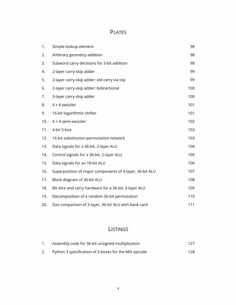
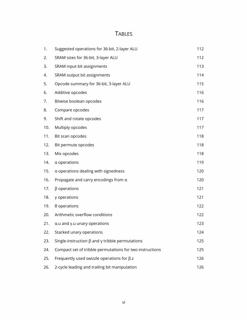