Embed Size (px)
DESCRIPTION
uuuu
Citation preview
1
Biologically inspired graphene-chlorophyll
phototransistors with high gain
Shao-Yu Chen1, Yi-Ying Lu1,2, Fu-Yu Shih1,3, Po-Hsun Ho4, Yang-Fang Chen3,
Chun-Wei Chen4, Yit-Tsong Chen1,2, and Wei-Hua Wang1*
1Institute of Atomic and Molecular Sciences, Academia Sinica, No. 1, Roosevelt Rd., Sec. 4, Taipei 106,
Taiwan
2Department of Chemistry, National Taiwan University, No. 1, Roosevelt Rd., Sec. 4, Taipei 106,
Taiwan
3Department of Physics, National Taiwan University, No. 1, Roosevelt Rd., Sec. 4, Taipei 106, Taiwan
4Department of Materials Science and Engineering, National Taiwan University, No. 1, Roosevelt Rd.,
Sec. 4, Taipei 106, Taiwan
*Corresponding Author.
Tel: +886-2-2366-8208, Fax: +886-2-2362-0200. E-mail address: [email protected] (W.-H. Wang)
2
Abstract
We present prominent photoresponse of bio-inspired graphene-based phototransistors sensitized with
chlorophyll molecules. The hybrid graphene-chlorophyll phototransistors exhibit a high gain of 610
electrons per photon and a high responsivity of 610 A/W, which can be attributed to the integration of
high-mobility graphene and the photosensitive chlorophyll molecules. The charge transfer at interface
and the photogating effect in the chlorophyll layer can account for the observed photoresponse of the
hybrid devices, which is confirmed by the back-gate-tunable photocurrent as well as the thickness and
time dependent studies of the photoresponse. The demonstration of the graphene-chlorophyll
phototransistors with high gain envisions a viable method to employ biomaterials for graphene-based
optoelectronics.
3
Manuscript text
1. Introduction
Graphene-based optoelectronic devices have been attracting great attention[1-3] and have promise for
future applications, such as solar cells, touch screens, and photodetectors.[4-6] The remarkable optical
properties of graphene, including its linear optical absorption[7, 8], tunable band-gap,[9] and intrinsic
photocurrent[10-13] have been demonstrated and can be integrated with other distinctively electronic
and mechanical properties of graphene for new functionalities. Pristine graphene suffers from weak
absorption as low as 2.3%, which fundamentally limits its applicability in photodetection. Consequently,
various approaches, including plasmonic effects,[14, 15] photothermoelectric effects,[16] and
sensitization by quantum dots[6, 17, 18] or bulk semiconductors,[19] have been employed to enhance
the interaction between graphene and photons. Here, we utilize chlorophyll as light absorbing materials
for graphene phototransistors and investigate the optoelectronic performance of the hybrid graphene-
chlorophyll devices. Chlorophyll is an organic semiconductor and is very efficient in light absorption.
Moreover, chlorophyll, as a biomaterial, is remarkably stable[20] and abundant. Given the crucial role
of chlorophyll in the photosynthesis process, studies of chlorophyll photosensitization may benefit
future applications, such as organic photovoltaics,[21, 22] optical sensors,[23] and artificial
photosynthesis.[24] Additionally, since there are many types of chlorophyll-related molecules, it is
possible to engineer the energy level alignment such that the charge separation and transfer are
optimized in the hybrid graphene-organic molecules systems.
In this paper, we present strong photoresponse observed in bio-inspired graphene-chlorophyll devices.
A pristine graphene/chlorophyll interface condition is achieved by employing resist-free fabrication
with in-situ and noncovalent functionalization. A high gain and a high responsivity of the hybrid
graphene-chlorophyll devices are demonstrated and attributed to the integration of the high-mobility
4
graphene and photosensitive chlorophyll molecules. Effective photogating effect originated from charge
separation/transfer can account for the observed large photoresponse, which is confirmed with the back-
gate-tunable photocurrent as well as the thickness and time dependent studies of the photoresponse.
2. Device Fabrication
A detailed description of the device fabrication and functionalization of chlorophyll a (Chla) can be
found in the supporting information (S1 and S2). We note that we have adapted careful procedures to
ensure a pristine graphene/Chla interface. First, monolayer graphene flakes were mechanically
exfoliated onto the octadecyltricholorosilanes (OTS)-functionalized substrates, and electrical contacts
were fabricated by resist-free approach to achieve a high mobility and a pristine graphene surface.[25]
Second, we performed laser annealing with excitation adjacent to the graphene devices, which greatly
reduced adsorbed molecules on the graphene surface (see supporting information S1). Third, we
employed controlled drop-casting[26] of Chla on-site of the cryostat with a continuous nitrogen gas
flow. Therefore, the cleanness of the graphene surface was preserved, which resulted in an optimum
contact condition between the Chla molecules and graphene. By following these careful procedures of
device fabrication, we achieved reproducible results on both sensitization and optoelectronic properties
of the phototransistors.
3. Results and Discussion
To confirm the effectiveness of surface functionalization, we performed Raman spectroscopy and
conductivity measurement on the graphene samples. Figure 1a shows the Raman spectrum of pristine
graphene (sample A) with an intensity ratio of 2D/G band of approximately 6 and a negligible D-band,
which indicates the high quality of the pristine graphene. After Chla functionalization, the Raman
spectrum reveals extra peaks in the range of 1000-1600 cm-1, which generally agrees with the resonance
spectra of the Chla film.[27] Moreover, we characterized the devices electrically by measuring the

5
conductance (G ) as a function of the gate voltage ( GV ). Figure 1b shows the G −VG curves of sample
A before and after Chla functionalization, which reveals the n-type doping characteristics as GV at the
charge neutrality point ( CNPV ) shifts from −5V to −40V. The n-type doping of graphene suggests that
the electrons transfer from Chla to graphene after the functionalization.
400 500 600 700
18.2
18.6
I sd
(μA
)
Abs
. Int
. (a.
u.)
λ (nm)
-80 -40 0 400
1
2
G (m
S)
VG (V)1000 2000 3000
2D
G
Int.
(arb
. uni
t)
Raman Shift (cm-1)
2D
Figure 1. (a) Raman spectra before (black curve) and after (red curve) Chla functionalization. A group
of Raman peaks in the range of 1000 ~ 1600 cm-1 are observed and are attributed to the Chla film. (b)
GVG − curves before (black curve) and after (red curve) Chla functionalization ( 100=SDV mV). A
reduction of mobility from 6500 to 1600 sVcm ⋅/2 for hole conduction and from 2700 to 1850
sVcm ⋅/2 for electron conduction was observed. (c) A schematic of the graphene-Chla device on an
OTS-functionalized substrate under illumination. (d) Photocurrent action spectrum of sample B (blue
curve). The two-peak structure observed at about 430 nm and 690 nm generally corresponds to the
absorption spectrum of the Chla solution (orange curve).
6
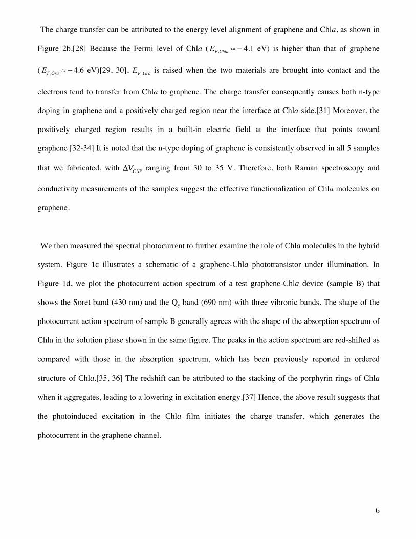
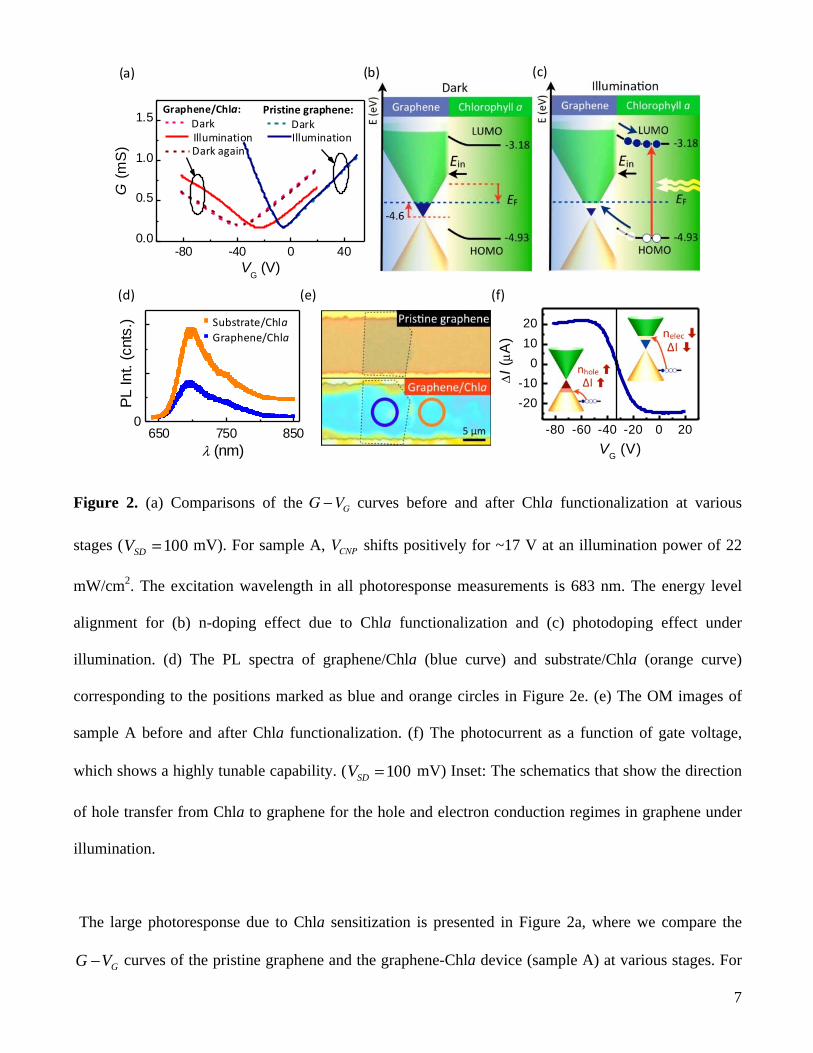
The charge transfer can be attributed to the energy level alignment of graphene and Chla, as shown in
Figure 2b.[28] Because the Fermi level of Chla (EF,Chla ≈ − 4.1 eV) is higher than that of graphene
(EF,Gra ≈ − 4.6 eV)[29, 30], GraFE , is raised when the two materials are brought into contact and the
electrons tend to transfer from Chla to graphene. The charge transfer consequently causes both n-type
doping in graphene and a positively charged region near the interface at Chla side.[31] Moreover, the
positively charged region results in a built-in electric field at the interface that points toward
graphene.[32-34] It is noted that the n-type doping of graphene is consistently observed in all 5 samples
that we fabricated, with CNPVΔ ranging from 30 to 35 V. Therefore, both Raman spectroscopy and
conductivity measurements of the samples suggest the effective functionalization of Chla molecules on
graphene.
We then measured the spectral photocurrent to further examine the role of Chla molecules in the hybrid
system. Figure 1c illustrates a schematic of a graphene-Chla phototransistor under illumination. In
Figure 1d, we plot the photocurrent action spectrum of a test graphene-Chla device (sample B) that
shows the Soret band (430 nm) and the Qy band (690 nm) with three vibronic bands. The shape of the
photocurrent action spectrum of sample B generally agrees with the shape of the absorption spectrum of
Chla in the solution phase shown in the same figure. The peaks in the action spectrum are red-shifted as
compared with those in the absorption spectrum, which has been previously reported in ordered
structure of Chla.[35, 36] The redshift can be attributed to the stacking of the porphyrin rings of Chla
when it aggregates, leading to a lowering in excitation energy.[37] Hence, the above result suggests that
the photoinduced excitation in the Chla film initiates the charge transfer, which generates the
photocurrent in the graphene channel.
7
-80 -40 0 400.0
0.5
1.0
1.5
G (m
S)
VG (V)
-80 -60 -40 -20 0 20
-20-10
01020
ΔI (
μA)
VG (V)650 750 850
PL In
t. (c
nts.
)
λ (nm)
0
Figure 2. (a) Comparisons of the G −VG curves before and after Chla functionalization at various
stages ( 100=SDV mV). For sample A, VCNP shifts positively for ~17 V at an illumination power of 22
mW/cm2. The excitation wavelength in all photoresponse measurements is 683 nm. The energy level
alignment for (b) n-doping effect due to Chla functionalization and (c) photodoping effect under
illumination. (d) The PL spectra of graphene/Chla (blue curve) and substrate/Chla (orange curve)
corresponding to the positions marked as blue and orange circles in Figure 2e. (e) The OM images of
sample A before and after Chla functionalization. (f) The photocurrent as a function of gate voltage,
which shows a highly tunable capability. ( 100=SDV mV) Inset: The schematics that show the direction
of hole transfer from Chla to graphene for the hole and electron conduction regimes in graphene under
illumination.
The large photoresponse due to Chla sensitization is presented in Figure 2a, where we compare the
GVG − curves of the pristine graphene and the graphene-Chla device (sample A) at various stages. For
8
pristine graphene, no significant photoresponse is observed with GV remaining at -5 V regardless of the
illumination power. By contrast, sample A exhibits a large photodoping effect, with VCNP shifting
substantially toward positive GV from -40 to -23 V. We note that the observed photoinduced doping in
this study is larger than that in the graphene systems sensitized with quantum dots[18] and C60,[38]
suggesting the uniqueness of the graphene-Chla system. The photoinduced carrier concentration in
sample A can be estimated by the equation 1210≈Δ= CNPVn α cm 2− , where α is the carrier density
capacitance of graphene. Furthermore, CNPV shifts back to -40 V after the laser irradiation, revealing a
reversible photoresponse process.
Here, we propose a qualitative model to account for the observed photoresponse in our samples (Figure
2c). The hole carriers in Chla are energetically favorable to transfer to graphene because the work
function of graphene is smaller than the ionization potential of Chla (-4.93 eV).[39] Moreover, this
charge transfer of the hole carriers is assisted by the built-in electric field at the interface that points
toward graphene. Accordingly, hole carriers are photoinduced in the Chla film, and those hole carriers
near the graphene/Chla interface are swept into graphene, which leads to efficient charge separation and
transfer. Conversely, the electron carriers tend to reside in the Chla layer due to the existence of the
built-in field. Therefore, the Chla film becomes more negatively charged, which induces positive charge
and p-type doping in graphene. The observed large photoinduced doping can be attributed to efficient
charge separation/transfer at the interface and the strong photogating effect due to the proximity of the
charged Chla molecules to graphene.
Next, we present photoluminescence (PL) and back-gate dependent photocurrent measurements that
further support the proposed model. We compare the PL of graphene-Chla and Chla on the substrate
(Figure 2d), which reveals an apparent quenching of PL in Chla on graphene. Because electron-hole
pairs are generated in the Chla molecules under illumination, the PL quenching suggest that charge
9
transfer occurs between the Chla film and graphene, which leads to reduction of radiative
recombination.[40] Moreover, the back-gate dependence of the photoresponse (Figure 2f) is also
consistent with the proposed model. We observed a strong carrier type and concentration dependence of
the photocurrent ( darklight III −≡Δ ), where IΔ is positive for hole conduction and negative for electron
conduction. In the hole conduction regime ( 33−<GV V), carrier concentration increases because excess
holes are induced by the photogating effect, which raises the conductance of graphene and a positive IΔ .
By contrast, the photoinduced hole carriers diminish the electron concentration, which leads to a
decreased conductance and a negative IΔ in the electron conduction regime ( 33−>GV V). Therefore,
the photocurrent of the device can be effectively tuned by back gate, and its polarity can also be
reversed.
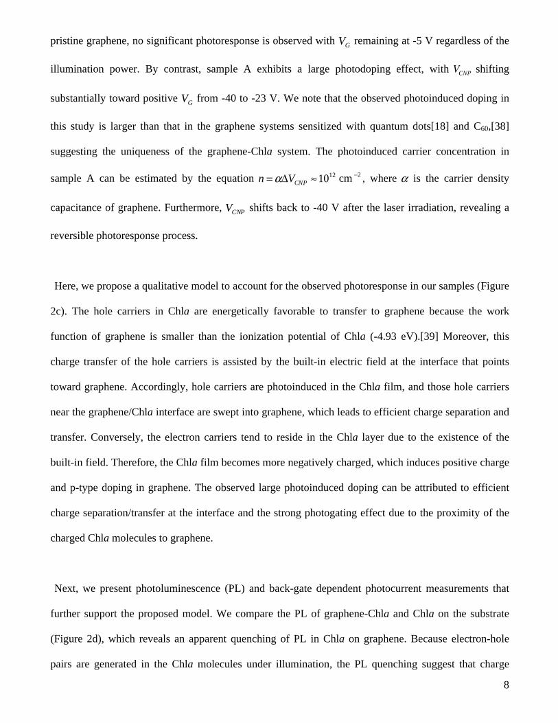
We can obtain the specifics of the devices from the power dependence of the photoresponse. Figures 3a
and 3b show the power dependent evolution of resistance ( R ) vs. GV curves for the pristine graphene
and sample A, respectively. Compared to relatively power independent CNPV of pristine graphene,
sample A exhibits a monotonic shift in CNPV toward positive GV . In Figure 3c, CNPVΔ monotonically
increases from 0 to 17 V with illumination power, which indicates an accumulative charge transfer
between Chla and graphene.[41] The photoinduced carrier concentration is 1210≈n cm 2− for 100=P
mW/cm2. CNPVΔ starts to level off at a high excitation power ( 1>P mW/cm2), suggesting that the
charge transfer begins to saturate. Regarding the transport characteristics, we observe that minimum
conductivity ( minσ ) decreased with an increasing excitation power as shown in Figure 3d. As discussed
earlier, the functionalization of graphene results in a positively charged Chla film, which causes charge
inhomogeneity in graphene.[42, 43] The charge transfer in the device under illumination reduces the
positive charging in Chla film, which leads to the reduction of charge inhomogeneity in graphene and
its minimum conductivity (supporting information S3). Therefore, the result suggests a trend toward the
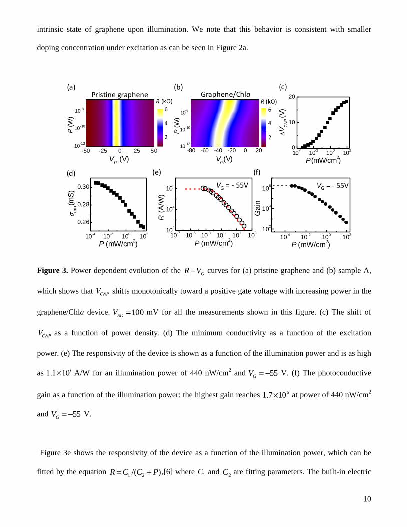
10
intrinsic state of graphene upon illumination. We note that this behavior is consistent with smaller
doping concentration under excitation as can be seen in Figure 2a.
10-4 10-2 100 102102
104
106
Gai
n
P (mW/cm2)10-4 10-2 100 102
0.26
0.28
0.30
σ min(m
S)
P (mW/cm2)
-80 -60 -40 -20 0 20
10-8
10-10
P (W
)
VG(V)
0.5000
1.875
3.250
4.625
6.000
10-12
-50 -25 0 25 50
10-8
10-10
P (W
)
VG (V)
10-120.5000
1.875
3.250
4.625
6.000
10-4 10-2 100 1020
10
20
ΔVCN
P(V
)
P (mW/cm2)
10-7 10-5 10-3 10-1 101 103102
104
106
R (A
/W)
P (mW/cm2)
Figure 3. Power dependent evolution of the GVR − curves for (a) pristine graphene and (b) sample A,
which shows that VCNP shifts monotonically toward a positive gate voltage with increasing power in the
graphene/Chla device. 100=SDV mV for all the measurements shown in this figure. (c) The shift of
VCNP as a function of power density. (d) The minimum conductivity as a function of the excitation
power. (e) The responsivity of the device is shown as a function of the illumination power and is as high
as 1.1×10⁶ A/W for an illumination power of 440 nW/cm2 and 55−=GV V. (f) The photoconductive
gain as a function of the illumination power: the highest gain reaches 6107.1 × at power of 440 nW/cm2
and 55−=GV V.
Figure 3e shows the responsivity of the device as a function of the illumination power, which can be
fitted by the equation )/( 21 PCCR += ,[6] where 1C and 2C are fitting parameters. The built-in electric
11
field, which causes the photoinduced doping in graphene, is reduced when more hole carriers are
transferred to graphene under higher power (Figure 2c). This consequently results in decreasing
responsivity at increasing illumination power. Notably, the responsivity reaches 610 A/W for an
illumination power of 440 nW/cm2, and the device can detect a laser power as low as 500 fW. The
responsivity in our device is comparable to that of graphene-based photodetectors previously
reported.[17, 18] We also calculated the photoconductive gain as a function of illumination power
(Figure 3f). The theoretical photoconductive gain thG , as defined by the ratio of the change of the
carriers in graphene to the change of the photons illuminated, can be written as
photon
SDth eA
VGφσ ⋅Δ= ,
where σΔ is the change in conductivity, SDV is the source-drain bias voltage, photonφ is the photon flux,
and A is the area of the graphene channel. For sample A, the optical gain is as high as 6107.1 × when
the power is 440 nW/cm2 and 55−=GV V. The high gain observed in our devices can be attributed to
the high mobility of graphene, which yields multiple hole circulations in the graphene channel while the
electrons remain trapped in the Chla layer by the built-in field.[6] The large photoresponse
characteristics observed in the hybrid graphene-chlorophyll devices suggests a feasible method of
utilizing highly stable biomaterials for graphene photosensitization.
A comparison of different thicknesses of the Chla film yields further insight into the photoresponse in
our devices. In Figure 4a, we compare the SDV dependence of IΔ for sample C (~50 nm) and D (~10
nm). The characterization for the thickness of Chla film is described in supporting information S2. The
photocurrent is found to be linearly increasing with bias voltage for VSD < 1 V. Based on Ohm’s law
)/( σWLIVSD = and the expression for conductivity hhen μσ = (hole conduction), we found that IΔ
varies linearly with SDV and that the slope is ΔI /VSD = Δnheμh (W / L)∝Δnh . Therefore, the slope in the

12
SDVI −Δ curves represents the magnitude of doping due to the photogating effect. We found that the
change in carrier concentration ( hnΔ ) enhances with increasing thickness, which is apparently
originated from the stronger photogating effect in the thicker Chla film. In Figure 4b, we show the
power dependence of the responsivity for samples C and D, which also manifests a clear thickness
dependence of the responsivity. Previous study on the interface between Chla and metal revealed an
exciton diffusion length of ~18 nm in the Chla film.[44] Therefore, it is possible that the carriers can
diffuse within the Chla film and subsequently transfer to graphene, causing the thickness dependent
photoresponse.
10-4 10-2 100 102
10-1
100
101 τ2
Resp
onse
Tim
e (s
)
P (mW/cm2)
τ1
0.0 0.5 1.0
38
39
40
I SD (μ
A)
t (s)
0.0 0.5 1.00
50
100
150
ΔI (μ
A)
Vsd
(V)10-4 10-2 100 102
102
104
106R
(A/W
)
P (mW/cm2)
Figure 4. (a) Photocurrent as a function of source-drain voltage for samples C (50 nm) and D (10 nm).
(b) Comparison of the responsivity for samples C and D. The saturated responsivity of samples C and D
are 6103.1 × and 3100.1 × A/W, respectively. (c) Temporal photocurrent dynamics of sample A for
55−=GV V and an excitation power of 22 mW/cm2. Both on and off periods are 200 ms. (d) The
excitation power dependence of the response time ( 21 ττ < ) for light (open squares) and dark (close
squares) periods.
13
Finally, we examined the photoresponse dynamics revealed by the time dependent measurement of the
photocurrent. Figure 4c shows the variation of the channel current of sample A for a sequence of on and
off periods of irradiation. In the hole conduction regime ( 55−=GV V), the device exhibits a positive
gain in photocurrent with photoexcitation on and a diminution after the illumination shuts off. Each time
dependence of the photocurrent can be fitted with two relaxations (supporting information S4), and the
power dependences of the response time ( 21 ττ < ) are shown in Figure 4d. We found that 2τ for on and
off follows a similar trend that remains near 10 s for all power range. On the contrary, 1τ exhibits a
stronger decaying tendency as the excitation power rises. Because IΔ is associated with the carrier
density change ( nΔ ) due to photogating, the tI −Δ curves represent the time dependence of charging
and discharging in the Chla film. Based on the time scale of the relaxation, it is possible that 1τ is
related to the photogating effect from the Chla molecules in close vicinity of graphene which leads to
the instant photocurrent change. We observe that 1τ decreases with increasing excitation power. This
behavior suggests that the transient photocurrent change is related to an instant surge in the hole carrier
concentration and resulting charge transfer, which are more intense under higher illumination power.
We note that the observed response time of the graphene-Chla device ( 11.0,1 =ONτ s and 45.0,1 =OFFτ s
for P=44 mW/cm2) is comparable to those in the graphene-PbS QDs phototransistors,[17] suggesting a
critical role of the graphene-photosensitizer interfaces with organic Chla molecules or ligand on PbS
QDs. Furthermore, the response time 2τ may be correlated with the carrier diffusion and/or trapping in
stacks of Chla molecules, which is dominated by the bulk Chla properties, such as mobility and trap
density.[17]
4. Conclusion
We have demonstrated the prominent photoresponse and the highly back-gate-tunable photocurrent in
the hybrid graphene-chlorophyll phototransistors. The devices exhibit a high gain of 106 electrons per
14
photon and a high responsivity of 106 A/W, which can be attributed to the integration of high-mobility
graphene and the light-absorbing chlorophyll molecules. The charge transfer at the interface and the
effective photogating effect in the chlorophyll layer can account for the observed large photoresponse,
which is confirmed by the thickness and time dependent studies of the photoresponse. The
demonstration of the graphene-chlorophyll phototransistors with high gain envisions a feasible method
to employ biomaterials for future graphene-based optoelectronics.
Acknowledgments
W.-H.W. thanks Juen-Kai Wang for the insightful discussions and Pin-Hao Sher for technical assistance.
This work was supported by the National Science Council of Taiwan under contract numbers NSC 101-
2112-M-001-020-MY2, NSC 101-2113-M-002-016-MY2, and NSC 100-2119-M-002-020.
Supporting Information Available. Device fabrication of graphene-chlorophyll phototransistors,
chlorophyll-a functionalization and characterization, power dependence of graphene transport
characteristics, and analysis of time-dependent photoresponse.
15
References:
[1] Bonaccorso F, Sun Z, Hasan T, Ferrari AC. Graphene photonics and optoelectronics. Nat Photonics. 2010;4(9):611-22. [2] Bao QL, Loh KP. Graphene Photonics, Plasmonics, and Broadband Optoelectronic Devices. Acs Nano. 2012;6(5):3677-94. [3] Avouris P, Xia FN. Graphene applications in electronics and photonics. MRS Bull. 2012;37(12):1225-34. [4] Miao XC, Tongay S, Petterson MK, Berke K, Rinzler AG, Appleton BR, et al. High Efficiency Graphene Solar Cells by Chemical Doping. Nano Lett. 2012;12(6):2745-50. [5] Bae S, Kim H, Lee Y, Xu XF, Park JS, Zheng Y, et al. Roll-to-roll production of 30-inch graphene films for transparent electrodes. Nat Nanotechnol. 2010;5(8):574-8. [6] Konstantatos G, Badioli M, Gaudreau L, Osmond J, Bernechea M, de Arquer FPG, et al. Hybrid graphene-quantum dot phototransistors with ultrahigh gain. Nat Nanotechnol. 2012;7(6):363-8. [7] Nair RR, Blake P, Grigorenko AN, Novoselov KS, Booth TJ, Stauber T, et al. Fine structure constant defines visual transparency of graphene. Science. 2008;320(5881):1308-. [8] Casiraghi C, Hartschuh A, Lidorikis E, Qian H, Harutyunyan H, Gokus T, et al. Rayleigh imaging of graphene and graphene layers. Nano Lett. 2007;7(9):2711-7. [9] Zhang YB, Tang TT, Girit C, Hao Z, Martin MC, Zettl A, et al. Direct observation of a widely tunable bandgap in bilayer graphene. Nature. 2009;459(7248):820-3. [10] Lee EJH, Balasubramanian K, Weitz RT, Burghard M, Kern K. Contact and edge effects in graphene devices. Nat Nanotechnol. 2008;3(8):486-90. [11] Mueller T, Xia F, Freitag M, Tsang J, Avouris P. Role of contacts in graphene transistors: A scanning photocurrent study. Phys Rev B. 2009;79(24):-. [12] Xu XD, Gabor NM, Alden JS, van der Zande AM, McEuen PL. Photo-Thermoelectric Effect at a Graphene Interface Junction. Nano Lett. 2010;10(2):562-6. [13] Freitag M, Low T, Xia FN, Avouris P. Photoconductivity of biased graphene. Nat Photonics. 2013;7(1):53-9. [14] Echtermeyer TJ, Britnell L, Jasnos PK, Lombardo A, Gorbachev RV, Grigorenko AN, et al. Strong plasmonic enhancement of photovoltage in graphene. Nat Commun. 2011;2:458. [15] Koppens FHL, Chang DE, de Abajo FJG. Graphene Plasmonics: A Platform for Strong Light-Matter Interactions. Nano Lett. 2011;11(8):3370-7. [16] Gabor NM, Song JCW, Ma Q, Nair NL, Taychatanapat T, Watanabe K, et al. Hot Carrier-Assisted Intrinsic Photoresponse in Graphene. Science. 2011;334(6056):648-52. [17] Sun ZH, Liu ZK, Li JH, Tai GA, Lau SP, Yan F. Infrared Photodetectors Based on CVD-Grown Graphene and PbS Quantum Dots with Ultrahigh Responsivity. Adv Mater. 2012;24(43):5878-83. [18] Zhang DY, Gan L, Cao Y, Wang Q, Qi LM, Guo XF. Understanding Charge Transfer at PbS-Decorated Graphene Surfaces toward a Tunable Photosensor. Adv Mater. 2012;24(20):2715-20. [19] Li XM, Zhu HW, Wang KL, Cao AY, Wei JQ, Li CY, et al. Graphene-On-Silicon Schottky Junction Solar Cells. Adv Mater. 2010;22(25):2743-8. [20] Liu ZM, Yasseri AA, Lindsey JS, Bocian DF. Molecular memories that survive silicon device processing and real-world operation. Science. 2003;302(5650):1543-5. [21] Campbell WM, Burrell AK, Officer DL, Jolley KW. Porphyrins as light harvesters in the dye-sensitised TiO2 solar cell. Coord Chem Rev. 2004;248(13-14):1363-79. [22] Spanggaard H, Krebs FC. A brief history of the development of organic and polymeric photovoltaics. Sol Energy Mater Sol Cells. 2004;83(2-3):125-46. [23] Hecht DS, Ramirez RJA, Briman M, Artukovic E, Chichak KS, Stoddart JF, et al. Bioinspired detection of light using a porphyrin-sensitized single-wall nanotube field effect transistor. Nano Lett. 2006;6(9):2031-6.
16
[24] Yamada H, Imahori H, Nishimura Y, Yamazaki I, Ahn TK, Kim SK, et al. Photovoltaic properties of self-assembled monolayers of porphyrins and porphyrin-fullerene dyads on ITO and gold surfaces. J Am Chem Soc. 2003;125(30):9129-39. [25] Chen SY, Ho PH, Shiue RJ, Chen CW, Wang WH. Transport/magnetotransport of high-performance graphene transistors on organic molecule-functionalized substrates. Nano Lett. 2012;12(2):964-9. [26] Star A, Lu Y, Bradley K, Gruner G. Nanotube optoelectronic memory devices. Nano Lett. 2004;4(9):1587-91. [27] Zhou CL, Diers JR, Bocian DF. Q(y)-excitation resonance Raman spectra of chlorophyll a and related complexes. Normal mode characteristics of the low-frequency vibrations. J Phys Chem B. 1997;101(46):9635-44. [28] Ishii H, Sugiyama K, Ito E, Seki K. Energy level alignment and interfacial electronic structures at organic/metal and organic/organic interfaces (vol 11, pg 605, 1999). Adv Mater. 1999;11(12):972-. [29] Yu YJ, Zhao Y, Ryu S, Brus LE, Kim KS, Kim P. Tuning the Graphene Work Function by Electric Field Effect. Nano Lett. 2009;9(10):3430-4. [30] Oshima C, Nagashima A. Ultra-thin epitaxial films of graphite and hexagonal boron nitride on solid surfaces. J Phys-Condens Mat. 1997;9(1):1-20. [31] Sze SM, Lee MK. Semiconductor devices, physics and technology. 3rd ed. Hoboken, N.J.: Wiley; 2012. [32] Neamen DA. Semiconductor physics and devices : basic principles. 2nd ed. Chicago: Irwin; 1997. [33] Ishii H, Seki K. Energy level alignment at organic/metal interfaces studied by UV photoemission: Breakdown of traditional assumption of a common vacuum level at the interface. Ieee T Electron Dev. 1997;44(8):1295-301. [34] Hill IG, Rajagopal A, Kahn A, Hu Y. Molecular level alignment at organic semiconductor-metal interfaces. Appl Phys Lett. 1998;73(5):662-4. [35] Tang CW, Albrecht AC. Photovoltaic Effects of Metal-Chlorophyll-a-Metal Sandwich Cells. J Chem Phys. 1975;62(6):2139-49. [36] Kassi H, Barazzouk S, Brullemans M, Leblanc RM, Hotchandani S. Photogeneration of charges in microcrystalline chlorophyll a. Thin Solid Films. 2010;518(18):5345-8. [37] Heithiert, H.; Ballschmiter, K.; Mohwald, H. Photochemistry and Photobiology 1983, 37, 201–205. [38] Jeon EK, Yang CS, Shen YF, Nakanishi T, Jeong DS, Kim JJ, et al. Photoconductivity and enhanced memory effects in hybrid C-60-graphene transistors. Nanotechnology. 2012;23(45):455202. [39] Nelson RC. Energy Levels in Chlorophyll and Electron Transfer Processes. Photochem Photobiol. 1968;8(5):441-50. [40] Wu HC, Huang YC, Ding IK, Chen CC, Yang YH, Tsai CC, et al. Photoinduced Electron Transfer in Dye-Sensitized SnO2 Nanowire Field-Effect Transistors. Adv Funct Mater. 2011;21(3):474-9. [41] Mok SM, Yan F, Chan HLW. Organic phototransistor based on poly(3-hexylthiophene)/TiO(2) nanoparticle composite. Appl Phys Lett. 2008;93(2):023310. [42] Tan YW, Zhang Y, Bolotin K, Zhao Y, Adam S, Hwang EH, et al. Measurement of scattering rate and minimum conductivity in graphene. Phys Rev Lett. 2007;99(24):246803. [43] Zhang YB, Brar VW, Girit C, Zettl A, Crommie MF. Origin of spatial charge inhomogeneity in graphene. Nat Phys. 2009;5(10):722-6. [44] Nasr C, Taleb T, Leblanc RM, Hotchandani S. Exciton diffusion length in microcrystalline chlorophyll a. Appl Phys Lett. 1996;69(13):1823-5.
Supporting Information for
Biologically inspired graphene-chlorophyll
phototransistors with high gain
Shao-Yu Chen1, Yi-Ying Lu1,2, Fu-Yu Shih1,3, Po-Hsun Ho4, Yang-Fang Chen3,
Chun-Wei Chen4, Yit-Tsong Chen1,2, and Wei-Hua Wang1*
1Institute of Atomic and Molecular Sciences, Academia Sinica, Taipei 106, Taiwan
2Department of Chemistry, National Taiwan University, Taipei 106, Taiwan
3Department of Physics, National Taiwan University, Taipei 106, Taiwan
4Department of Materials Science and Engineering, National Taiwan University, Taipei 106,
Taiwan
*Corresponding Author.
Tel: +886-2-2366-8208, Fax: +886-2-2362-0200. E-mail address: [email protected] (W.-H.
Wang)
S1. Device fabrication of graphene-chlorophyll phototransistors
Monolayer graphene sheets were mechanically exfoliated on the OTS-functionalized SiO2 (300
nm)/Si substrate. The OTS-functionalized SiO2/Si substrates can effectively reduce charged
impurity scattering due to adsorbed molecules and the phonon effect, which is coupled to the
substrates. Consequently, graphene on OTS-functionalized SiO2/Si substrates exhibits high
mobility, which is important for the demonstration of the large photoresponse. We applied both
optical contrast and Raman spectroscopy to identify the single-layer graphene (SLG) sheets. We
adopted the resist-free fabrication technique to avoid undesirable contamination through the
lithography processes. After alignment of the SLG sheets and the shadow mask (commercial
TEM grid) under the optical microscope (OM), we deposited electrodes with Ti/Au (5 nm/55
nm) by using an electron-beam evaporator at a base pressure of approximately 1.0 ×10⁻⁷ torr.
The channel length of the graphene devices is 12 μ m.
After metallization, the graphene device was subsequently transferred into a cryostat (Janis
Research Company, ST-500) for the initial characterization. The pressure in the cryostat is
2.0 ×10⁻⁷ torr. Before characterization, we performed local laser annealing by focusing the laser
(532 nm, 10 mW, spot size: 1μ m) adjacent to the device for 2 hours to remove the surface
adsorbates, such as H2O and O2 molecules in ambient conditions. The laser intensity on the
sample is estimated to be 2.4 mW/ μ m2. Local laser annealing is preferred over thermal heating,
which may introduce cross contaminations from other part of the samples.
The electrical measurements were performed by using Keithley 237 source-measurement unit
for the DC resistance measurement ( 100=SDV mV for all measurements) and Keithley 2400 for
back gate voltage. In the photoresponse measurements, we chose the semiconductor diode laser
with a wavelength of 683 nm as a coherent light source. We note that the excitation wavelength
for all photoresponse measurements is chosen to be approximately the peak value in the
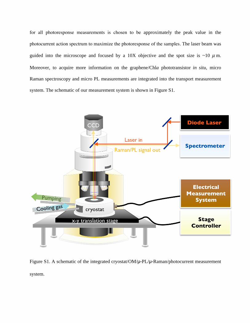
photocurrent action spectrum to maximize the photoresponse of the samples. The laser beam was
guided into the microscope and focused by a 10X objective and the spot size is ~10 μ m.
Moreover, to acquire more information on the graphene/Chla phototransistor in situ, micro
Raman spectroscopy and micro PL measurements are integrated into the transport measurement
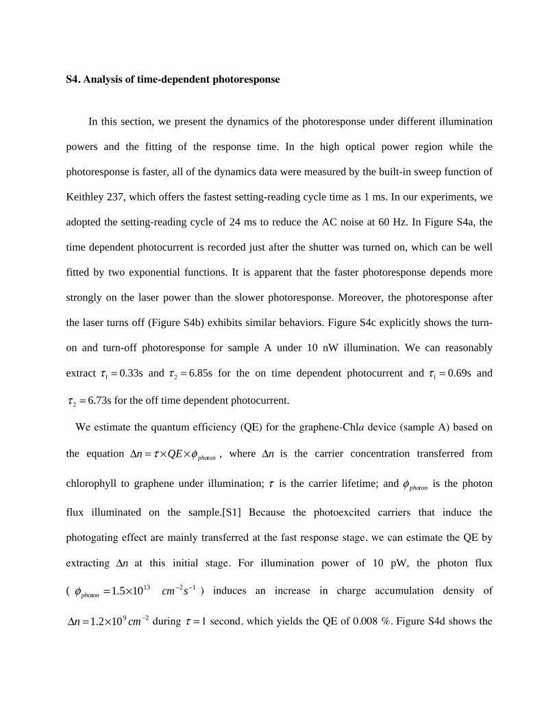
system. The schematic of our measurement system is shown in Figure S1.
Figure S1. A schematic of the integrated cryostat/OM/ PL/ Raman/photocurrent measurement
system.
S2. Chlorophyll-a modification and thickness characterization
We chose Chla because it is a light-absorbing material that exhibits good absorption in the
visible-light spectrum for the graphene-based phototransistor. We applied commercial Chla
powder (Sigma Aldrich, 99.9%) and stored it in the refrigerator at −20°C . We chose ether as a
solvent to prepare the Chla solution of 1.5 and 50 μ M following the functionalization procedure.
In this article, we used the drop-casting method to functionalize the graphene devices with Chla
molecules. The thickness of Chla layer can be determined by AFM with specific calibration
procedure.
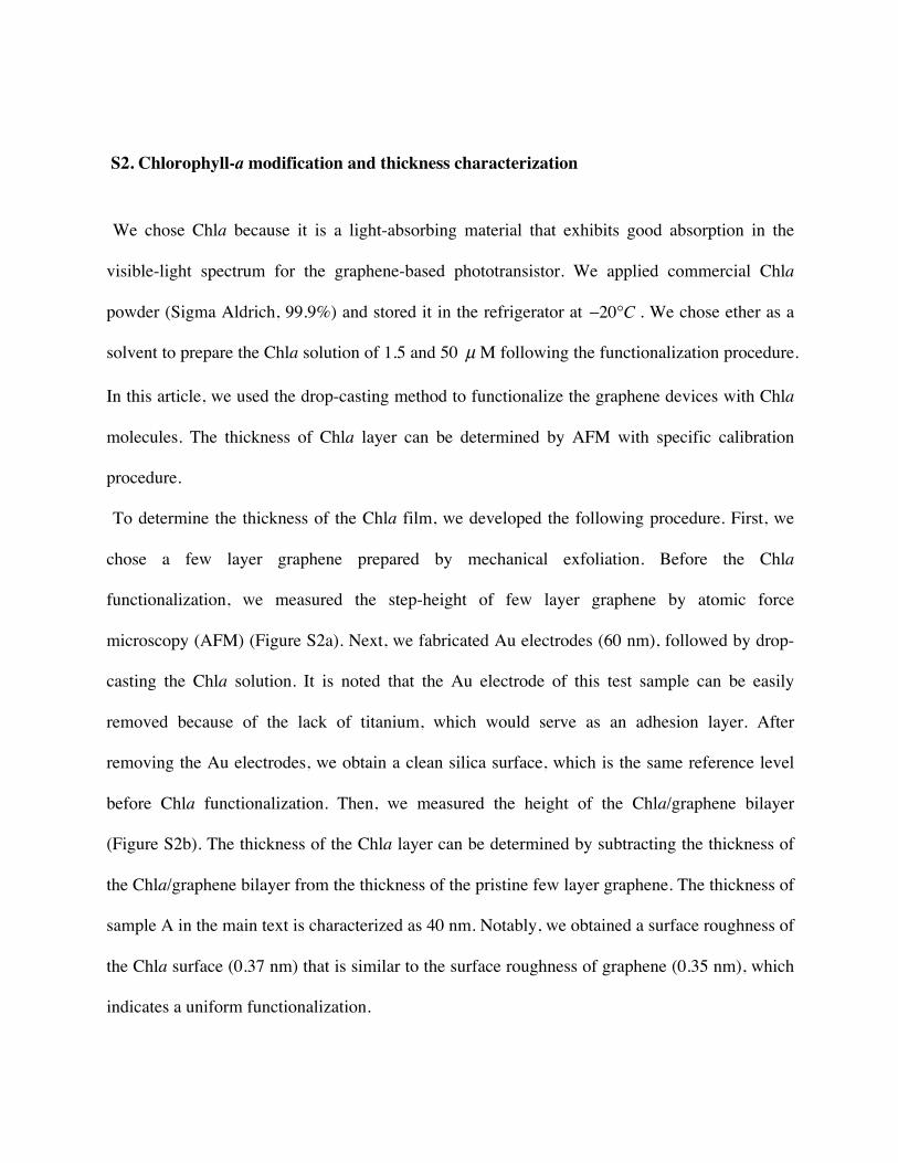
To determine the thickness of the Chla film, we developed the following procedure. First, we
chose a few layer graphene prepared by mechanical exfoliation. Before the Chla
functionalization, we measured the step-height of few layer graphene by atomic force
microscopy (AFM) (Figure S2a). Next, we fabricated Au electrodes (60 nm), followed by drop-
casting the Chla solution. It is noted that the Au electrode of this test sample can be easily
removed because of the lack of titanium, which would serve as an adhesion layer. After
removing the Au electrodes, we obtain a clean silica surface, which is the same reference level
before Chla functionalization. Then, we measured the height of the Chla/graphene bilayer
(Figure S2b). The thickness of the Chla layer can be determined by subtracting the thickness of
the Chla/graphene bilayer from the thickness of the pristine few layer graphene. The thickness of
sample A in the main text is characterized as 40 nm. Notably, we obtained a surface roughness of
the Chla surface (0.37 nm) that is similar to the surface roughness of graphene (0.35 nm), which
indicates a uniform functionalization.
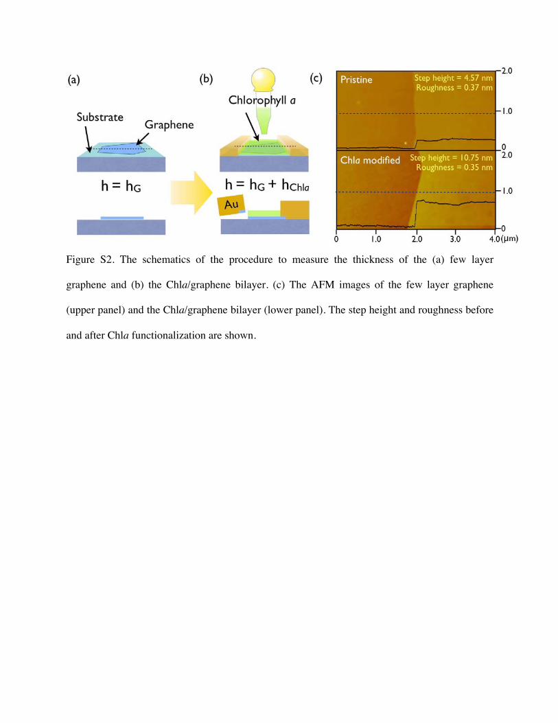
Figure S2. The schematics of the procedure to measure the thickness of the (a) few layer
graphene and (b) the Chla/graphene bilayer. (c) The AFM images of the few layer graphene
(upper panel) and the Chla/graphene bilayer (lower panel). The step height and roughness before
and after Chla functionalization are shown.
S3. Power dependence of graphene transport characteristics
We showed that the minimum conductivity decreases as the excitation power increases (Figure
3d in the main text), which indicates a trend toward the intrinsic state of graphene. This behavior
is consistently observed in our samples as shown in Figure S3 (upper panel), which may be
attributed to the decreased charge inhomogeneity in graphene caused by the decrease in number
of charged sites in the Chla film. Moreover, we observed an increasing electron and hole
mobility with increasing excitation power, as shown in Figure S3 (lower panel). The n-type
doping due to the Chla film results in a reduction in mobility due to charged impurity scattering.
The charge transfer in the device reduces the n-type doping effect, which leads to a revived
electron and hole mobility. This trend is generally valid, although sample-to-sample variation
also exists.
10-3 10-1 101
1.6
1.8
2.0
μ (1
03 cm
2/V
.s)
P (mW/cm2)
10-3 10-1 1010.28
0.30
0.32
σ min(m
S)
P (mW/cm2)10-3 10-1 101
0.260.280.300.320.34
σ min(m
S)
P (mW/cm2)10-3 10-1 101
0.35
0.40
0.45
0.50
0.55
σ min(m
S)
P (mW/cm2)10-3 10-1 101
0.260.280.300.320.34
σ min(m
S)
P (mW/cm2)
10-3 10-1 1011.5
2.0
2.5
3.0
3.5
μ (1
03 cm
2 /V.s
)
P (mW/cm2)
10-3 10-1 101
2.0
2.5
3.0
3.5
μ (1
03 c
m2/V
.s)
P (mW/cm2)10-3 10-1 101
2.4
2.8
μ (1
03 cm
2 /V.s
)
P (mW/cm2)

Figure S3. Minimum conductivity (upper panel) and electron/hole mobility (lower panel) as a
function of excitation power for samples A, C, D, and E.
S4. Analysis of time-dependent photoresponse
In this section, we present the dynamics of the photoresponse under different illumination
powers and the fitting of the response time. In the high optical power region while the
photoresponse is faster, all of the dynamics data were measured by the built-in sweep function of
Keithley 237, which offers the fastest setting-reading cycle time as 1 ms. In our experiments, we
adopted the setting-reading cycle of 24 ms to reduce the AC noise at 60 Hz. In Figure S4a, the
time dependent photocurrent is recorded just after the shutter was turned on, which can be well
fitted by two exponential functions. It is apparent that the faster photoresponse depends more
strongly on the laser power than the slower photoresponse. Moreover, the photoresponse after
the laser turns off (Figure S4b) exhibits similar behaviors. Figure S4c explicitly shows the turn-
on and turn-off photoresponse for sample A under 10 nW illumination. We can reasonably
extract τ1 = 0.33s and τ 2 = 6.85s for the on time dependent photocurrent and τ1 = 0.69s and
τ 2 = 6.73s for the off time dependent photocurrent.
We estimate the quantum efficiency (QE) for the graphene-Chla device (sample A) based on
the equation photonQEn φτ ××=Δ , where nΔ is the carrier concentration transferred from
chlorophyll to graphene under illumination; τ is the carrier lifetime; and photonφ is the photon
flux illuminated on the sample.[S1] Because the photoexcited carriers that induce the
photogating effect are mainly transferred at the fast response stage, we can estimate the QE by
extracting nΔ at this initial stage. For illumination power of 10 pW, the photon flux
( 13105.1 ×=photonφ 12 −− scm ) induces an increase in charge accumulation density of
29102.1 −×=Δ cmn during =τ 1 second, which yields the QE of 0.008 %. Figure S4d shows the
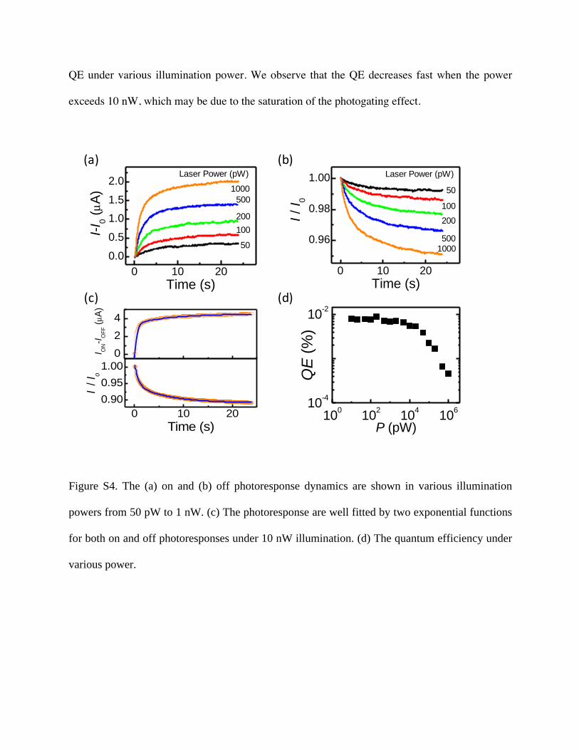
QE under various illumination power. We observe that the QE decreases fast when the power
exceeds 10 nW, which may be due to the saturation of the photogating effect.
0 10 200.0
0.5
1.01.5
2.0Laser Power (pW)
1000500
200100
50
I-I0 (μ
A)
Time (s)
0 10 200.900.951.00
I / Io
Time (s)
024
I ON-I O
FF (μ
A)
0 10 20
0.96
0.98
1.00 Laser Power (pW)
50
100
200
5001000
I / I 0
Time (s)
100 102 104 10610-4
10-2
Q
E (%
)
P (pW)
Figure S4. The (a) on and (b) off photoresponse dynamics are shown in various illumination
powers from 50 pW to 1 nW. (c) The photoresponse are well fitted by two exponential functions
for both on and off photoresponses under 10 nW illumination. (d) The quantum efficiency under
various power.

REFERENCE:
[S1] Konstantatos G, Badioli M, Gaudreau L, Osmond J, Bernechea M, de Arquer FPG, et al.
Hybrid graphene-quantum dot phototransistors with ultrahigh gain. Nat Nanotechnol.
2012;7(6):363-8


