Embed Size (px)
Citation preview
2009-12-16 1385DX_DS_Ver2.1 Inphi Proprietary Page 1 of 23
1385DX 12.5 Gbps 1:8 Demultiplexer with Latched Comparator Input Data Sheet
Applications
• Broadband test and measurement • Automatic Test Equipment (ATE) • Military/Aerospace Instrumentation • Broadband Digital Cross-Connects
Features
• 1:8 DEMUX (to 12.5 Gbps) • High-sensitivity latched comparator input
• Automatic synchronization of multiple 1385DX demultiplexers
• Front-end bandwidth: 14 GHz typical • Low power consumption: 1.5 W typical • Clock rates of DC to 12.5 GHz typical • Differential CML I/O with common mode adjust• Differential, selectable-rate output clock,
including half-rate • Single, +3.3 V power supply • Available in 8x8 mm QFN
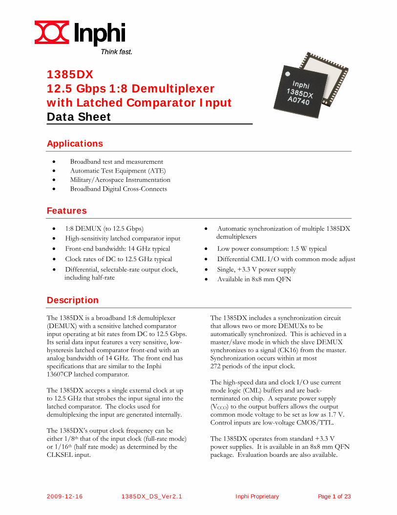
Description The 1385DX is a broadband 1:8 demultiplexer (DEMUX) with a sensitive latched comparator input operating at bit rates from DC to 12.5 Gbps. Its serial data input features a very sensitive, low-hysteresis latched comparator front-end with an analog bandwidth of 14 GHz. The front end has specifications that are similar to the Inphi 13607CP latched comparator. The 1385DX accepts a single external clock at up to 12.5 GHz that strobes the input signal into the latched comparator. The clocks used for demultiplexing the input are generated internally. The 1385DX’s output clock frequency can be either 1/8th that of the input clock (full-rate mode) or 1/16th (half rate mode) as determined by the CLKSEL input.
The 1385DX includes a synchronization circuit that allows two or more DEMUXs to be automatically synchronized. This is achieved in a master/slave mode in which the slave DEMUX synchronizes to a signal (CK16) from the master. Synchronization occurs within at most 272 periods of the input clock. The high-speed data and clock I/O use current mode logic (CML) buffers and are back-terminated on chip. A separate power supply (VCCO) to the output buffers allows the output common mode voltage to be set as low as 1.7 V. Control inputs are low-voltage CMOS/TTL. The 1385DX operates from standard +3.3 V power supplies. It is available in an 8x8 mm QFN package. Evaluation boards are also available.
2009-12-16 1385DX_DS_Ver2.1 Inphi Proprietary Page 2 of 23
Block Diagram
1:2DX
D0
CK16
CLKIN
SYN
EN
D4
D2
D6
D1
D5
D3
D7
1:4DX
C3 C4
1:4DX
C3 C4
INC2
Clock Generator
C1 C2 C4 C8 C16
SOUT
SCLK2SCLK1SE CSMR
MA
NR
ST
CLK
SEL
LCC1
SCLK
1
SCLK
2
SYNC
CKOUT2:1Sel
Figure 1. Block diagram. Not all connections are shown, and, though the block diagram does not show it, many of the I/O are differential.
2009-12-16 1385DX_DS_Ver2.1 Inphi Proprietary Page 3 of 23
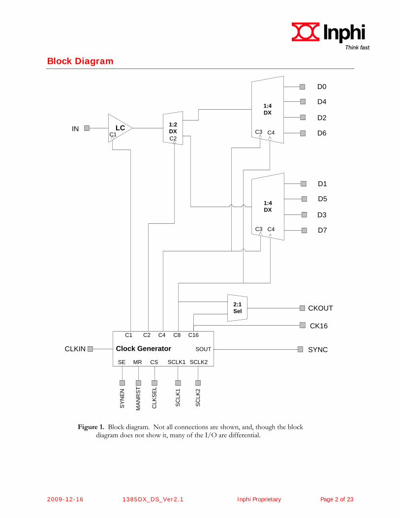
Absolute Maximum Ratings
• Stresses beyond those listed here may cause permanent damage to the device. • These are stress ratings only. Functional operation of the device at these or any other conditions beyond
those indicated in the “Operating Conditions” and “Electrical Specifications” of this datasheet is not implied. • Exposure to absolute maximum rating conditions for extended periods may affect device reliability.
Parameter Min Max Unit
Digital Power Supply Level (VCCD) 1 -0.5 3.8 V
Analog Power Supply Level (VCCA)1 -0.5 3.8 V
Output Buffer Power Supply Level (VCCO) 1 -0.5 3.8 V
Power Supply Difference (Digital to Analog) |VCCD - VCCA| 1 --- 0.6 V
Power Supply Difference (Digital to Output) VCCD - VCCO -0.6 2.0 V
Ground difference (Digital to Analog) |GND - GNDA| 2 --- 0.6 V Data Input Signals VCCA - 2 VCCA + 0.6 V Clock Input Signals VCCD - 2 VCCD + 0.6 V Control Inputs -0.5 VCCD + 0.6 V Data and CKOUT Outputs -0.5 VCCO + 1.0 V CK16 Outputs -0.5 VCCD + 1.0 V Low Frequency LVCMOS outputs -0.5 VCCD + 1.0 V Case Temperature –55 +125 °C Shipping/Storage Temperature –55 +125 °C Humidity 0 100 % ESD Protection – Data Inputs: INP, INN (Human Body Model) 350 --- V ESD Protection – All other Input and Output pins (HBM) 500 --- V ESD Protection – Power Supplies (HBM) 500 --- V Note: 1 The Analog power supply (VCCA) and Digital supply (VCCD) should be connected together on the board. 2 The Analog ground (GNDA) and Digital ground (GND) should be connected together on the board.
2009-12-16 1385DX_DS_Ver2.1 Inphi Proprietary Page 4 of 23
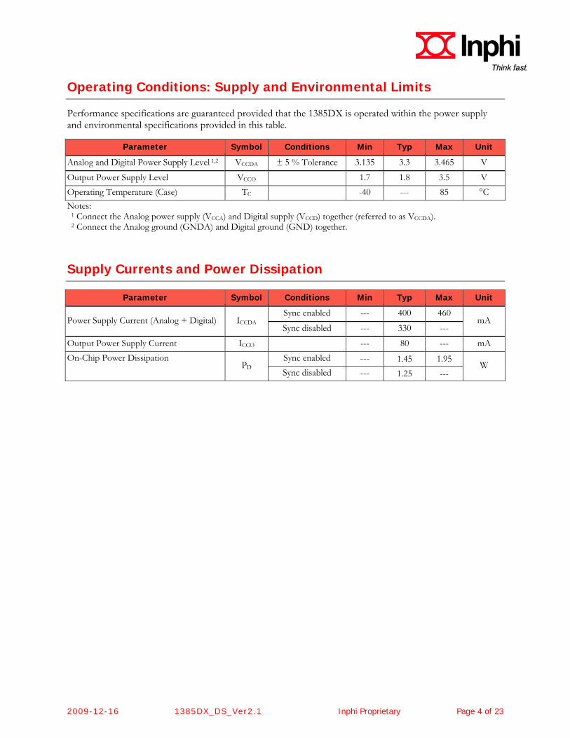
Operating Conditions: Supply and Environmental Limits Performance specifications are guaranteed provided that the 1385DX is operated within the power supply and environmental specifications provided in this table.
Parameter Symbol Conditions Min Typ Max Unit
Analog and Digital Power Supply Level 1,2 VCCDA ± 5 % Tolerance 3.135 3.3 3.465 V
Output Power Supply Level VCCO 1.7 1.8 3.5 V Operating Temperature (Case) TC -40 --- 85 °C Notes: 1 Connect the Analog power supply (VCCA) and Digital supply (VCCD) together (referred to as VCCDA). 2 Connect the Analog ground (GNDA) and Digital ground (GND) together.
Supply Currents and Power Dissipation
Parameter Symbol Conditions Min Typ Max Unit
Power Supply Current (Analog + Digital) ICCDA Sync enabled --- 400 460
mA Sync disabled --- 330 ---
Output Power Supply Current ICCO --- 80 --- mA On-Chip Power Dissipation
PD Sync enabled --- 1.45 1.95
W Sync disabled --- 1.25 ---
2009-12-16 1385DX_DS_Ver2.1 Inphi Proprietary Page 5 of 23
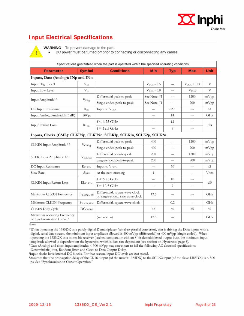
Input Electrical Specifications
WARNING – To prevent damage to the part: • DC power must be turned off prior to connecting or disconnecting any cables.
Specifications guaranteed when the part is operated within the specified operating conditions.
Parameter Symbol Conditions Min Typ Max Unit
Inputs, Data (Analog): INp and INn
Input High Level VIH VCCA - 0.5 --- VCCA + 0.3 V
Input Low Level VIL VCCA - 0.8 --- VCCA V
Input Amplitude1,2 VINpp Differential peak-to-peak See Note #1 --- 1200 mVpp
Single-ended peak-to-peak See Note #1 --- 700 mVpp
DC Input Resistance RIN Input to VCCA --- 62.5 --- Ω
Input Analog Bandwidth (3 dB) BWIN --- 14 --- GHz
Input Return Loss RLIN f < 6.25 GHz --- 12 ---
dB f = 12.5 GHz --- 8 ---
Inputs, Clocks (CML): CLKINp, CLKINn, SCLK1p, SCLK1n, SCLK2p, SCLK2n
CLKIN Input Amplitude 2,3 VCLKpp Differential peak-to-peak 400 --- 1200 mVpp
Single-ended peak-to-peak 400 --- 700 mVpp
SCLK Input Amplitude 2,3 VSCLKpp Differential peak-to-peak 200 --- 1200 mVpp
Single-ended peak-to-peak 200 --- 700 mVpp
DC Input Resistance RCLKIN Input to VCCD --- 50 --- Ω
Slew Rate SMIN At the zero crossing 1 --- --- V/ns
CLKIN Input Return Loss RLCLKIN f < 6.25 GHz --- 10 ---
dB f = 12.5 GHz --- 7 ---
Maximum CLKIN Frequency fCLKIN,MAX Differential, square wave clock or Single-ended, sine wave clock 12.5 --- --- GHz
Minimum CLKIN Frequency fCLKIN,MIN Differential, square wave clock --- 0.2 --- GHz
CLKIN Duty Cycle DCCLKIN 45 50 55 %
Maximum operating Frequency of Synchronization Circuit4 (see note 4) 12.5 --- GHz
Notes: 1 When operating the 1385DX as a purely digital Demultiplexer (serial-to-parallel converter), that is driving the Data inputs with a digital, serial data stream, the minimum input amplitude allowed is 400 mVpp (differential) or 400 mVpp (single-ended). When operating the 1385DX as a mono-bit receiver (latched comparator with an 8-bit demultiplexed output bus), the minimum input amplitude allowed is dependent on the hysteresis, which is data rate dependent (see section on Hysteresis, page 8).
2 Data (Analog) and clock input amplitudes < 300 mVpp may cause part to fail the following AC electrical specifications: Deterministic Jitter, Random Jitter, and Clock to Data Output Delay.
3Input clocks have internal DC blocks. For that reason, input DC levels are not stated. 4Assumes that the propagation delay of the CK16 output (of the master 1385DX) to the SCLK2 input (of the slave 1385DX) is < 500
ps. See “Synchronization Circuit Operation.”
!
2009-12-16 1385DX_DS_Ver2.1 Inphi Proprietary Page 6 of 23
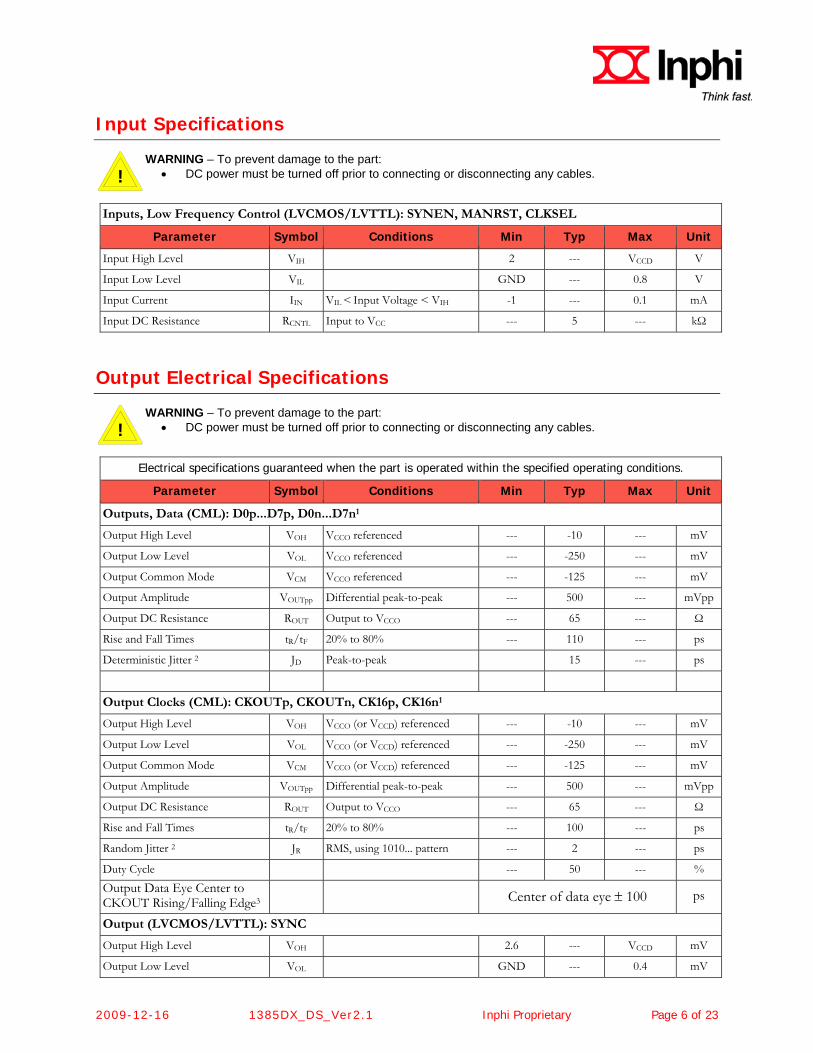
Input Specifications
WARNING – To prevent damage to the part: • DC power must be turned off prior to connecting or disconnecting any cables.
Inputs, Low Frequency Control (LVCMOS/LVTTL): SYNEN, MANRST, CLKSEL
Parameter Symbol Conditions Min Typ Max Unit
Input High Level VIH 2 --- VCCD V
Input Low Level VIL GND --- 0.8 V
Input Current IIN VIL < Input Voltage < VIH -1 --- 0.1 mA
Input DC Resistance RCNTL Input to VCC --- 5 --- kΩ
Output Electrical Specifications
WARNING – To prevent damage to the part:
• DC power must be turned off prior to connecting or disconnecting any cables.
Electrical specifications guaranteed when the part is operated within the specified operating conditions.
Parameter Symbol Conditions Min Typ Max Unit
Outputs, Data (CML): D0p...D7p, D0n...D7n1
Output High Level VOH VCCO referenced --- -10 --- mV
Output Low Level VOL VCCO referenced --- -250 --- mV
Output Common Mode VCM VCCO referenced --- -125 --- mV
Output Amplitude VOUTpp Differential peak-to-peak --- 500 --- mVpp
Output DC Resistance ROUT Output to VCCO --- 65 --- Ω
Rise and Fall Times tR/tF 20% to 80% --- 110 --- ps
Deterministic Jitter 2 JD Peak-to-peak 15 --- ps
Output Clocks (CML): CKOUTp, CKOUTn, CK16p, CK16n1
Output High Level VOH VCCO (or VCCD) referenced --- -10 --- mV
Output Low Level VOL VCCO (or VCCD) referenced --- -250 --- mV
Output Common Mode VCM VCCO (or VCCD) referenced --- -125 --- mV
Output Amplitude VOUTpp Differential peak-to-peak --- 500 --- mVpp
Output DC Resistance ROUT Output to VCCO --- 65 --- Ω
Rise and Fall Times tR/tF 20% to 80% --- 100 --- ps
Random Jitter 2 JR RMS, using 1010... pattern --- 2 --- ps
Duty Cycle --- 50 --- % Output Data Eye Center to CKOUT Rising/Falling Edge3
Center of data eye ± 100 ps
Output (LVCMOS/LVTTL): SYNC
Output High Level VOH 2.6 --- VCCD mV
Output Low Level VOL GND --- 0.4 mV
!
!
2009-12-16 1385DX_DS_Ver2.1 Inphi Proprietary Page 7 of 23
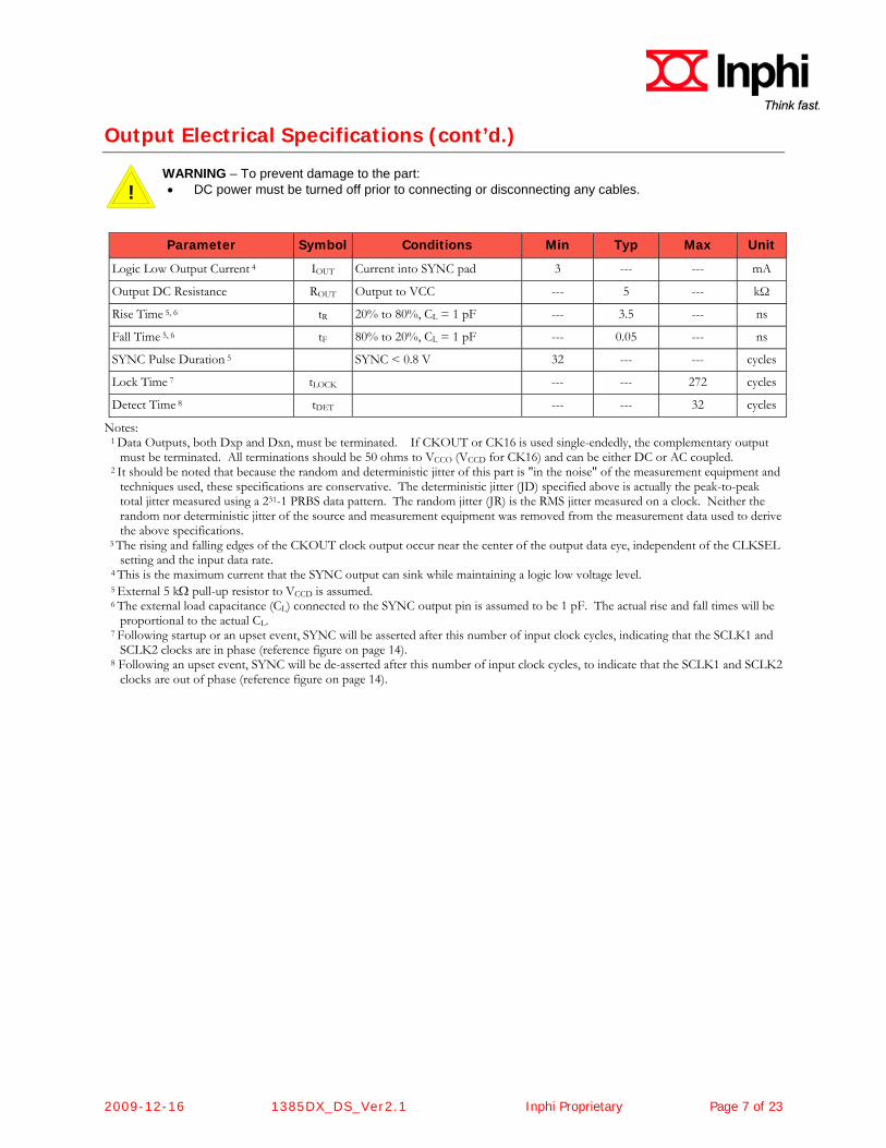
Output Electrical Specifications (cont’d.)
WARNING – To prevent damage to the part: • DC power must be turned off prior to connecting or disconnecting any cables.
Parameter Symbol Conditions Min Typ Max Unit
Logic Low Output Current 4 IOUT Current into SYNC pad 3 --- --- mA
Output DC Resistance ROUT Output to VCC --- 5 --- kΩ
Rise Time 5, 6 tR 20% to 80%, CL = 1 pF --- 3.5 --- ns
Fall Time 5, 6 tF 80% to 20%, CL = 1 pF --- 0.05 --- ns
SYNC Pulse Duration 5 SYNC < 0.8 V 32 --- --- cycles
Lock Time 7 tLOCK --- --- 272 cycles
Detect Time 8 tDET --- --- 32 cycles
Notes: 1 Data Outputs, both Dxp and Dxn, must be terminated. If CKOUT or CK16 is used single-endedly, the complementary output
must be terminated. All terminations should be 50 ohms to VCCO (VCCD for CK16) and can be either DC or AC coupled. 2 It should be noted that because the random and deterministic jitter of this part is "in the noise" of the measurement equipment and
techniques used, these specifications are conservative. The deterministic jitter (JD) specified above is actually the peak-to-peak total jitter measured using a 231-1 PRBS data pattern. The random jitter (JR) is the RMS jitter measured on a clock. Neither the random nor deterministic jitter of the source and measurement equipment was removed from the measurement data used to derive the above specifications.
3 The rising and falling edges of the CKOUT clock output occur near the center of the output data eye, independent of the CLKSEL setting and the input data rate.
4 This is the maximum current that the SYNC output can sink while maintaining a logic low voltage level. 5 External 5 kΩ pull-up resistor to VCCD is assumed. 6 The external load capacitance (CL) connected to the SYNC output pin is assumed to be 1 pF. The actual rise and fall times will be
proportional to the actual CL. 7 Following startup or an upset event, SYNC will be asserted after this number of input clock cycles, indicating that the SCLK1 and
SCLK2 clocks are in phase (reference figure on page 14). 8 Following an upset event, SYNC will be de-asserted after this number of input clock cycles, to indicate that the SCLK1 and SCLK2
clocks are out of phase (reference figure on page 14).
!
2009-12-16 1385DX_DS_Ver2.1 Inphi Proprietary Page 8 of 23
Hysteresis Characteristics
Delta VOUT versus Delta VIN
-0.8
-0.6
-0.4
-0.2
0.0
0.2
0.4
0.6
0.8
-10 -5 0 5 10
Delta Vin (mV)
Del
ta V
out (
V)
-5 C25 C55 C85 C
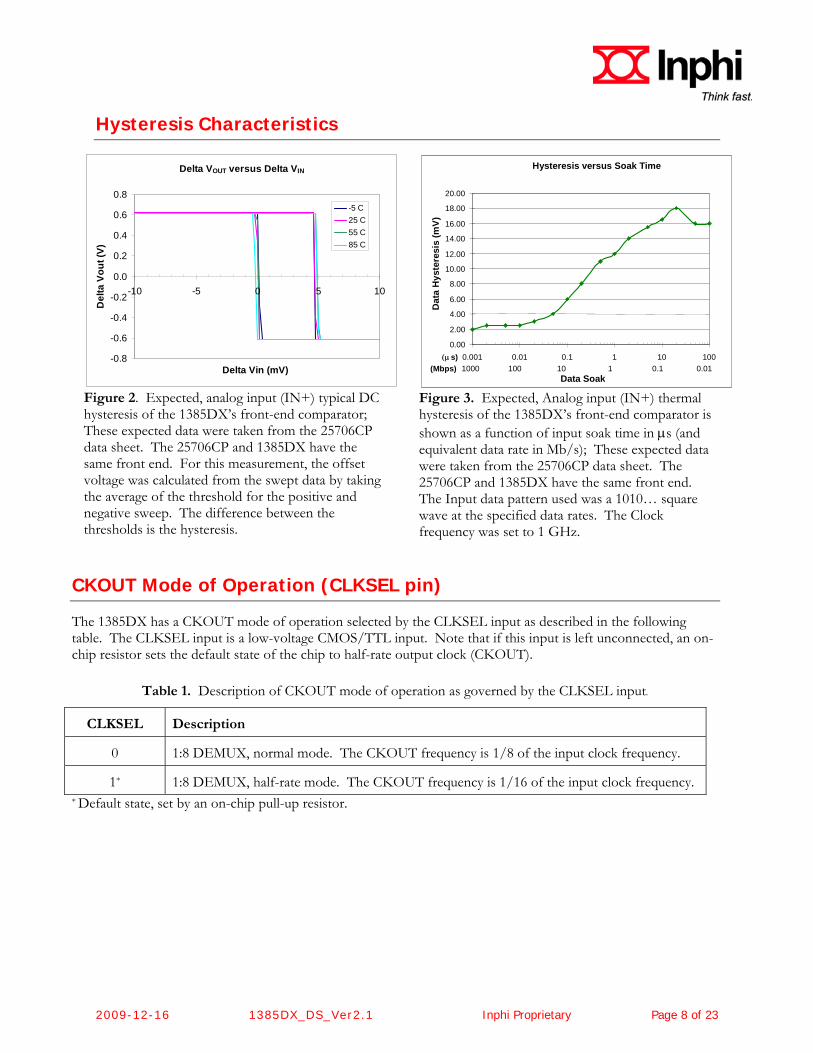
Figure 2. Expected, analog input (IN+) typical DC hysteresis of the 1385DX’s front-end comparator; These expected data were taken from the 25706CP data sheet. The 25706CP and 1385DX have the same front end. For this measurement, the offset voltage was calculated from the swept data by taking the average of the threshold for the positive and negative sweep. The difference between the thresholds is the hysteresis.
Hysteresis versus Soak Time
0.00
2.00
4.00
6.00
8.00
10.00
12.00
14.00
16.00
18.00
20.00
0.001 0.01 0.1 1 10 100
Data Soak
Dat
a H
yste
resi
s (m
V)
1000 100 10 1 0.1 0.01(μs)
(Mbps)
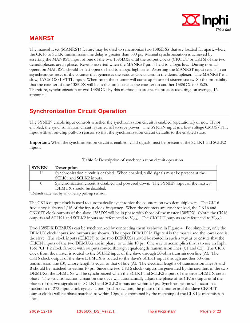
Figure 3. Expected, Analog input (IN+) thermal hysteresis of the 1385DX’s front-end comparator is shown as a function of input soak time in μs (and equivalent data rate in Mb/s); These expected data were taken from the 25706CP data sheet. The 25706CP and 1385DX have the same front end. The Input data pattern used was a 1010… square wave at the specified data rates. The Clock frequency was set to 1 GHz.
CKOUT Mode of Operation (CLKSEL pin) The 1385DX has a CKOUT mode of operation selected by the CLKSEL input as described in the following table. The CLKSEL input is a low-voltage CMOS/TTL input. Note that if this input is left unconnected, an on-chip resistor sets the default state of the chip to half-rate output clock (CKOUT).
Table 1. Description of CKOUT mode of operation as governed by the CLKSEL input.
CLKSEL Description
0 1:8 DEMUX, normal mode. The CKOUT frequency is 1/8 of the input clock frequency.
1* 1:8 DEMUX, half-rate mode. The CKOUT frequency is 1/16 of the input clock frequency. * Default state, set by an on-chip pull-up resistor.
2009-12-16 1385DX_DS_Ver2.1 Inphi Proprietary Page 9 of 23
MANRST The manual reset (MANRST) feature may be used to synchronize two 1385DXs that are located far apart, where the CK16 to SCLK transmission line delay is greater than 500 ps. Manual synchronization is achieved by asserting the MANRST input of one of the two 1385DXs until the output clocks (CKOUT or CK16) of the two demultiplexers are in phase. Reset is asserted when the MANRST pin is held to a logic low. During normal operation MANRST should be left open or held to a logic high state. Asserting the MANRST input results in an asynchronous reset of the counter that generates the various clocks used in the demultiplexer. The MANRST is a slow, LVCMOS/LVTTL input. When reset, the counter will come up in one of sixteen states. So the probability that the counter of one 1385DX will be in the same state as the counter on another 1385DX is 0.0625. Therefore, synchronization of two 1385DXs by this method is a stochastic process requiring, on average, 16 attempts. Synchronization Circuit Operation The SYNEN enable input controls whether the synchronization circuit is enabled (operational) or not. If not enabled, the synchronization circuit is turned off to save power. The SYNEN input is a low-voltage CMOS/TTL input with an on-chip pull-up resistor so that the synchronization circuit defaults to the enabled state. Important: When the synchronization circuit is enabled, valid signals must be present at the SCLK1 and SCLK2 inputs.
Table 2: Description of synchronization circuit operation
SYNEN Description 1* Synchronization circuit is enabled. When enabled, valid signals must be present at the
SCLK1 and SCLK2 inputs. 0 Synchronization circuit is disabled and powered down. The SYNEN input of the master
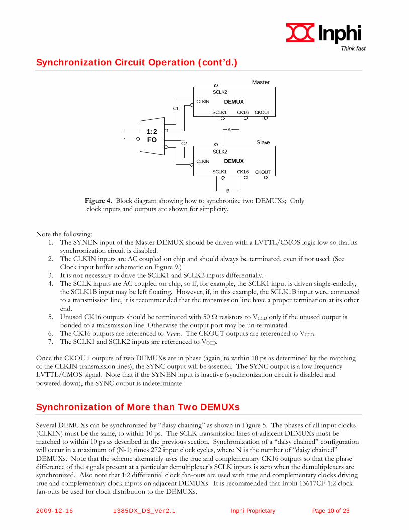
DEMUX should be disabled. * Default state, set by an on-chip pull-up resistor. The CK16 output clock is used to automatically synchronize the counters on two demultiplexers. The CK16 frequency is always 1/16 of the input clock frequency. When the counters are synchronized, the CK16 and CKOUT clock outputs of the slave 1385DX will be in phase with those of the master 1385DX. (Note: the CK16 outputs and SCLK1 and SCLK2 inputs are referenced to VCCD. The CKOUT outputs are referenced to VCCO). Two 1385DX DEMUXs can be synchronized by connecting them as shown in Figure 4. For simplicity, only the DEMUX clock inputs and outputs are shown. The upper DEMUX in Figure 4 is the master and the lower one is the slave. The clock inputs (CLKIN) to the two DEMUXs should be routed in such a way as to ensure that the CLKIN inputs of the two DEMUXs are in phase, to within 10 ps. One way to accomplish this is to use an Inphi 13617CF 1:2 clock fan-out with outputs routed through equal-length transmission lines (C1 and C2). The CK16 clock from the master is routed to the SCLK2 input of the slave through 50-ohm transmission line (A). The CK16 clock output of the slave DEMUX is routed to the slave’s SCLK1 input through another 50-ohm transmission line (B), whose length is equal to that of line (A). The electrical lengths of transmission lines A and B should be matched to within 10 ps. Since the two CK16 clock outputs are generated by the counters in the two DEMUXs, the DEMUXs will be synchronized when the SCLK1 and SCLK2 inputs of the slave DEMUX are in phase. The synchronization circuit on the slave will automatically adjust the phase of its CK16 output until the phases of the two signals at its SCLK1 and SCLK2 inputs are within 20 ps. Synchronization will occur in a maximum of 272 input clock cycles. Upon synchronization, the phase of the master and the slave CKOUT output clocks will be phase matched to within 10ps, as determined by the matching of the CLKIN transmission lines.
2009-12-16 1385DX_DS_Ver2.1 Inphi Proprietary Page 10 of 23
Synchronization Circuit Operation (cont’d.)
Master
C1
DEMUX
CLK8SCLK2
SCLK1
CLK16
CLKIN DEMUX
CK16SCLK1
SCLK2
CKOUT
CLKIN
DEMUX
CK16SCLK2
SCLK1
CLK16
CLKIN DEMUX
CK16SCLK1
SCLK2
CKOUT
CLKIN
B
A
C2
1:2FO Slave
Figure 4. Block diagram showing how to synchronize two DEMUXs; Only clock inputs and outputs are shown for simplicity.
Note the following:
1. The SYNEN input of the Master DEMUX should be driven with a LVTTL/CMOS logic low so that its synchronization circuit is disabled.
2. The CLKIN inputs are AC coupled on chip and should always be terminated, even if not used. (See Clock input buffer schematic on Figure 9.)
3. It is not necessary to drive the SCLK1 and SCLK2 inputs differentially. 4. The SCLK inputs are AC coupled on chip, so if, for example, the SCLK1 input is driven single-endedly,
the SCLK1B input may be left floating. However, if, in this example, the SCLK1B input were connected to a transmission line, it is recommended that the transmission line have a proper termination at its other end.
5. Unused CK16 outputs should be terminated with 50 Ω resistors to VCCD only if the unused output is bonded to a transmission line. Otherwise the output port may be un-terminated.
6. The CK16 outputs are referenced to VCCD. The CKOUT outputs are referenced to VCCO. 7. The SCLK1 and SCLK2 inputs are referenced to VCCD.
Once the CKOUT outputs of two DEMUXs are in phase (again, to within 10 ps as determined by the matching of the CLKIN transmission lines), the SYNC output will be asserted. The SYNC output is a low frequency LVTTL/CMOS signal. Note that if the SYNEN input is inactive (synchronization circuit is disabled and powered down), the SYNC output is indeterminate.
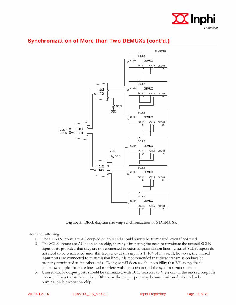
Synchronization of More than Two DEMUXs Several DEMUXs can be synchronized by “daisy chaining” as shown in Figure 5. The phases of all input clocks (CLKIN) must be the same, to within 10 ps. The SCLK transmission lines of adjacent DEMUXs must be matched to within 10 ps as described in the previous section. Synchronization of a “daisy chained” configuration will occur in a maximum of (N-1) times 272 input clock cycles, where N is the number of “daisy chained” DEMUXs. Note that the scheme alternately uses the true and complementary CK16 outputs so that the phase difference of the signals present at a particular demultiplexer’s SCLK inputs is zero when the demultiplexers are synchronized. Also note that 1:2 differential clock fan-outs are used with true and complementary clocks driving true and complementary clock inputs on adjacent DEMUXs. It is recommended that Inphi 13617CF 1:2 clock fan-outs be used for clock distribution to the DEMUXs.
2009-12-16 1385DX_DS_Ver2.1 Inphi Proprietary Page 11 of 23
Synchronization of More than Two DEMUXs (cont’d.)
MASTER
DEMUX
CLK8SCLK2
SCLK1
CLK16
CLKIN DEMUX
CK16SCLK1
SCLK2
CKOUT
CLKIN
DEMUX
CLK8SCLK2
SCLK1
CLK16
CLKIN DEMUX
CK16SCLK1
SCLK2
CKOUT
CLKIN
DEMUX
CLK8SCLK2
SCLK1
CLK16
CLKIN DEMUX
CK16SCLK1
SCLK2
CKOUT
CLKIN
1:2FO
1:2FO
1:2FO
DEMUX
CK16SCLK2
SCLK1
CLK16
CLKIN DEMUX
CK16SCLK1
SCLK2
CKOUT
CLKIN
50 Ω
VCC
50 Ω
VCC
CLKINCLKIN
DEMUX
CLK8SCLK2
SCLK1
CLK16
CLKIN DEMUX
CK16SCLK1
SCLK2
CKOUT
CLKIN
DEMUX
CLK8SCLK2
SCLK1
CLK16
CLKIN DEMUX
CK16SCLK1
SCLK2
CKOUT
CLKIN
Figure 5. Block diagram showing synchronization of 6 DEMUXs.
Note the following:
1. The CLKIN inputs are AC coupled on chip and should always be terminated, even if not used. 2. The SCLK inputs are AC coupled on chip, thereby eliminating the need to terminate the unused SCLK
input ports provided that they are not connected to external transmission lines. Unused SCLK inputs do not need to be terminated since this frequency at this input is 1/16th of fCLKIN. If, however, the unused input ports are connected to transmission lines, it is recommended that these transmission lines be properly terminated at the other ends. Doing so will decrease the possibility that RF energy that is somehow coupled to these lines will interfere with the operation of the synchronization circuit.
3. Unused CK16 output ports should be terminated with 50 Ω resistors to VCCD only if the unused output is connected to a transmission line. Otherwise the output port may be un-terminated, since a back-termination is present on-chip.
2009-12-16 1385DX_DS_Ver2.1 Inphi Proprietary Page 12 of 23
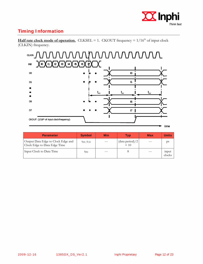
Timing Information Half rate clock mode of operation. CLKSEL = 1. CKOUT frequency = 1/16th of input clock (CLKIN) frequency.
D7
D6
D1
D0
time
CLKIN
CKOUT (1/16th of input clock frequency)
tDC
I0
I1
I6
I7
IN0 I0 I1 I2 I3 I5 I6 I7I4
tCDtPD
D7
D6
D1
D0
timetime
CLKIN
CKOUT (1/16th of input clock frequency)
tDC
I0
I1
I6
I7
IN0 I0 I1 I2 I3 I5 I6 I7I4IN0 I0 I1 I2 I3 I5 I6 I7I4
tCDtPD
Parameter Symbol Min Typ Max Units
Output Data Edge to Clock Edge and Clock Edge to Data Edge Time
tDC, tCD --- (data period)/2 + 10
--- ps
Input Clock to Data Time tPD --- 8 --- input clocks
2009-12-16 1385DX_DS_Ver2.1 Inphi Proprietary Page 13 of 23
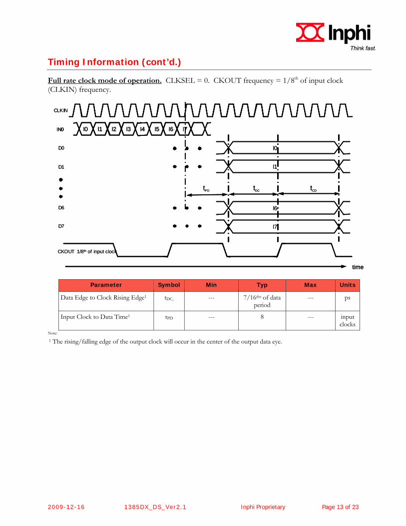
Timing Information (cont’d.) Full rate clock mode of operation. CLKSEL = 0. CKOUT frequency = 1/8th of input clock (CLKIN) frequency.
D7
D6
D1
D0
time
CLKIN
CKOUT 1/8th of input clock
tDC
I0
I1
I6
I7
IN0 I0 I1 I2 I3 I5 I6 I7I4
tCDtPD
D7
D6
D1
D0
timetime
CLKIN
CKOUT 1/8th of input clock
tDC
I0
I1
I6
I7
IN0 I0 I1 I2 I3 I5 I6 I7I4IN0 I0 I1 I2 I3 I5 I6 I7I4
tCDtPD
Parameter Symbol Min Typ Max Units
Data Edge to Clock Rising Edge1 tDC, --- 7/16ths of data period
--- ps
Input Clock to Data Time1 tPD --- 8 --- input clocks
Note:
1 The rising/falling edge of the output clock will occur in the center of the output data eye.
2009-12-16 1385DX_DS_Ver2.1 Inphi Proprietary Page 14 of 23
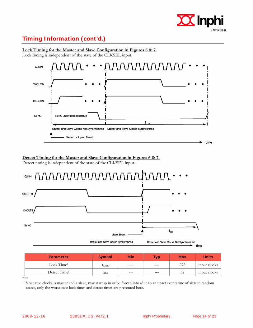
Timing Information (cont’d.) Lock Timing for the Master and Slave Configuration in Figures 6 & 7. Lock timing is independent of the state of the CLKSEL input.
time
CLKIN
CKOUTM
CKOUTS
SYNC
Master and Slave Clocks SynchronizedMaster and Slave Clocks Not Synchronized
Startup or Upset Event
tLOCK
SYNC undefined at startup
timetime
CLKIN
CKOUTM
CKOUTS
SYNC
Master and Slave Clocks SynchronizedMaster and Slave Clocks Not Synchronized
Startup or Upset Event
tLOCK
SYNC undefined at startup
Detect Timing for the Master and Slave Configuration in Figures 6 & 7. Detect timing is independent of the state of the CLKSEL input.
time
CLKIN
CKOUTM
CKOUTS
SYNC
tDET
Master and Slave Clocks Synchronized Master and Slave Clocks Not Synchronized
Upset Event
timetime
CLKIN
CKOUTM
CKOUTS
SYNC
tDET
Master and Slave Clocks Synchronized Master and Slave Clocks Not Synchronized
Upset Event
Parameter Symbol Min Typ Max Units
Lock Time1 tLock --- --- 272 input clocks
Detect Time1 tDet --- --- 32 input clocks Note:
1 Since two clocks, a master and a slave, may startup in or be forced into (due to an upset event) one of sixteen random states, only the worst-case lock times and detect times are presented here.
2009-12-16 1385DX_DS_Ver2.1 Inphi Proprietary Page 15 of 23
Typical Operating Characteristics
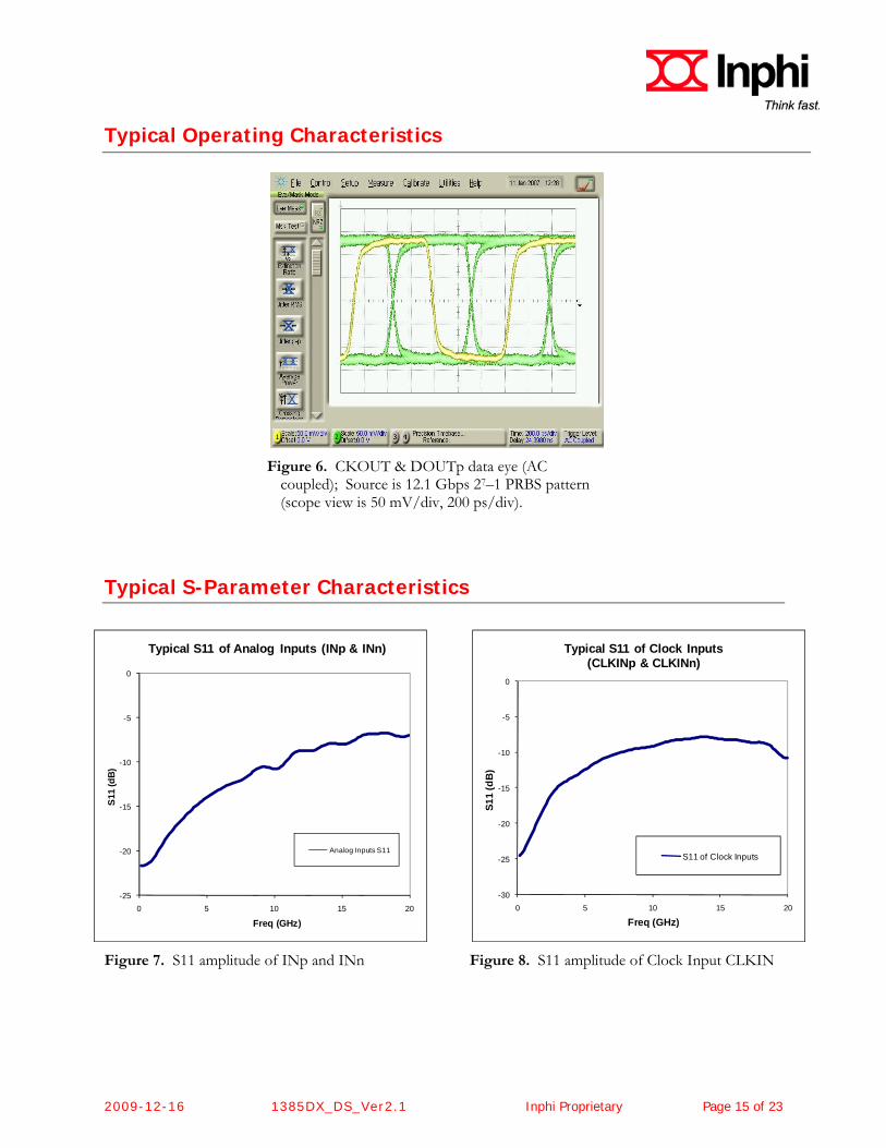
Figure 6. CKOUT & DOUTp data eye (AC
coupled); Source is 12.1 Gbps 27–1 PRBS pattern (scope view is 50 mV/div, 200 ps/div).
Typical S-Parameter Characteristics
Figure 7. S11 amplitude of INp and INn
Figure 8. S11 amplitude of Clock Input CLKIN
-25
-20
-15
-10
-5
0
0 5 10 15 20
S11
(dB)
Freq (GHz)
Typical S11 of Analog Inputs (INp & INn)
Analog Inputs S11
-30
-25
-20
-15
-10
-5
0
0 5 10 15 20
S11
(dB
)
Freq (GHz)
Typical S11 of Clock Inputs(CLKINp & CLKINn)
S11 of Clock Inputs
2009-12-16 1385DX_DS_Ver2.1 Inphi Proprietary Page 16 of 23
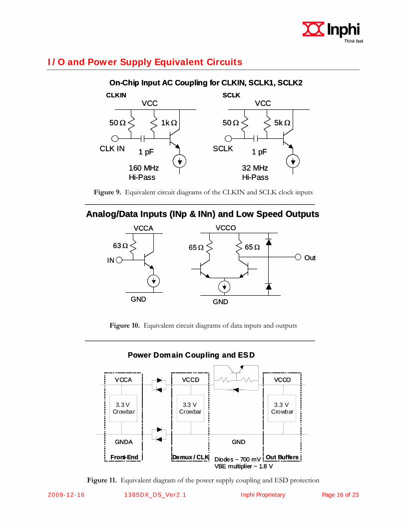
I/O and Power Supply Equivalent Circuits
50 Ω 5k Ω
1 pF
VCC
SCLK
32 MHz Hi-Pass
On-Chip Input AC Coupling for CLKIN, SCLK1, SCLK2
50 Ω 1k Ω
1 pF
VCC
CLK IN
160 MHz Hi-Pass
SCLKCLKIN
50 Ω 5k Ω
1 pF
VCC
SCLK
32 MHz Hi-Pass
On-Chip Input AC Coupling for CLKIN, SCLK1, SCLK2
50 Ω 1k Ω
1 pF
VCC
CLK IN
160 MHz Hi-Pass
SCLKCLKIN
Figure 9. Equivalent circuit diagrams of the CLKIN and SCLK clock inputs
Analog/Data Inputs (INp & INn) and Low Speed OutputsVCCA
GND
IN
VCCO
GND
Out
63 Ω 65 Ω 65 Ω
Analog/Data Inputs (INp & INn) and Low Speed OutputsVCCA
GND
IN
VCCO
GND
Out
63 Ω 65 Ω 65 Ω
Figure 10. Equivalent circuit diagrams of data inputs and outputs
3.3 V Crowbar
VCCA
GNDA
3.3 V Crowbar
VCCD
GND
VCCO
1.8 V Crowbar
Front - End Demux / CLK Out Buffers Diodes ~ 700 mVVBE multiplier ~ 1.8 V
Power Domain Coupling and ESD
3.3 V Crowbar
VCCA
GNDA
3.3 V Crowbar
VCCD
GND
VCCO
3.3 V Crowbar
Front - End Demux / CLK Out Buffers Diodes ~ 700 mVVBE multiplier ~ 1.8 V
Power Domain Coupling and ESD
Figure 11. Equivalent diagram of the power supply coupling and ESD protection
2009-12-16 1385DX_DS_Ver2.1 Inphi Proprietary Page 17 of 23
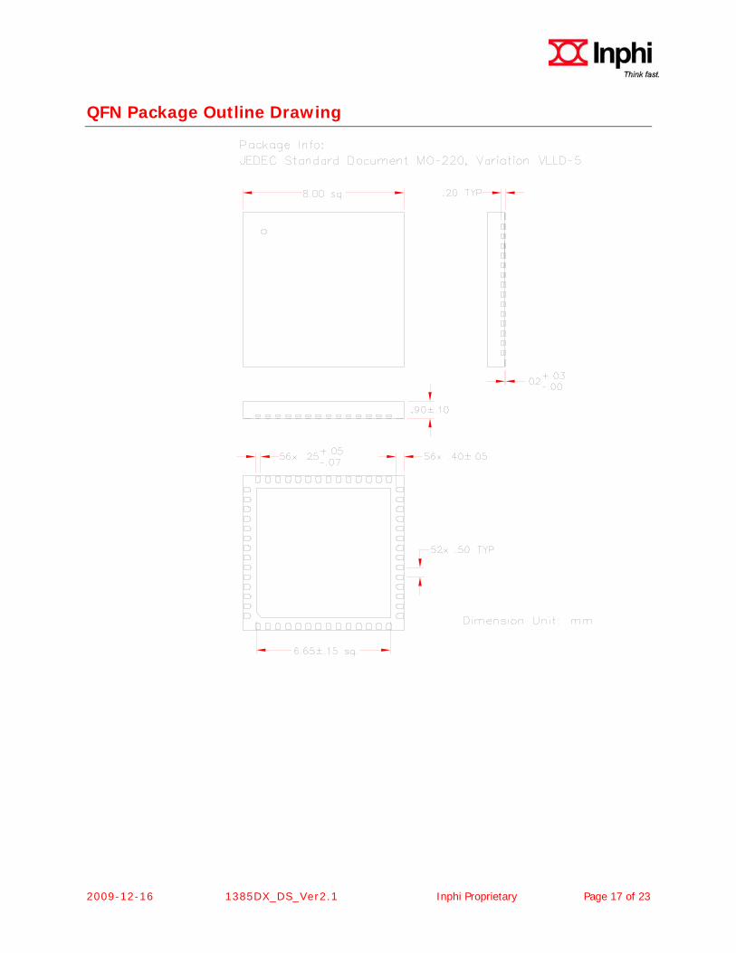
QFN Package Outline Drawing
2009-12-16 1385DX_DS_Ver2.1 Inphi Proprietary Page 18 of 23
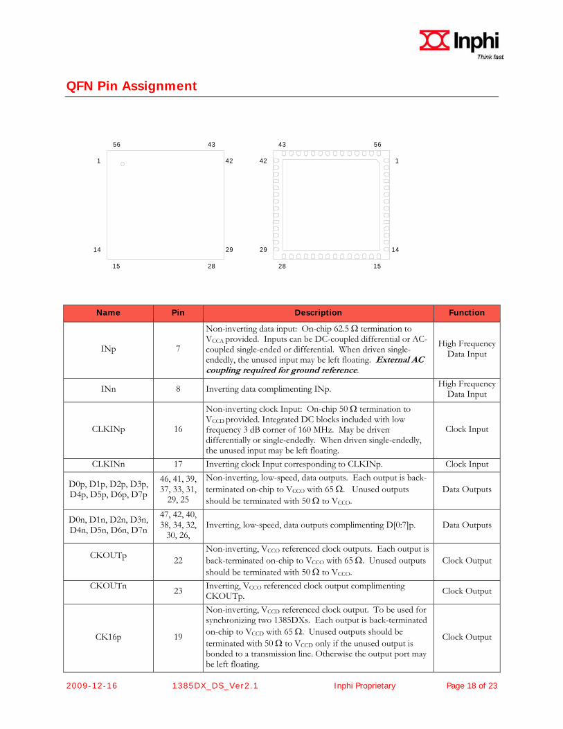
QFN Pin Assignment
1
14
42
29
56 43
15 28
1
14
42
29
43
28
56
15
Name Pin Description Function
INp 7
Non-inverting data input: On-chip 62.5 Ω termination to VCCA provided. Inputs can be DC-coupled differential or AC-coupled single-ended or differential. When driven single-endedly, the unused input may be left floating. External AC coupling required for ground reference.
High Frequency Data Input
INn 8 Inverting data complimenting INp. High Frequency Data Input
CLKINp 16
Non-inverting clock Input: On-chip 50 Ω termination to VCCD provided. Integrated DC blocks included with low frequency 3 dB corner of 160 MHz. May be driven differentially or single-endedly. When driven single-endedly, the unused input may be left floating.
Clock Input
CLKINn 17 Inverting clock Input corresponding to CLKINp. Clock Input
D0p, D1p, D2p, D3p, D4p, D5p, D6p, D7p
46, 41, 39, 37, 33, 31,
29, 25
Non-inverting, low-speed, data outputs. Each output is back-terminated on-chip to VCCO with 65 Ω. Unused outputs should be terminated with 50 Ω to VCCO.
Data Outputs
D0n, D1n, D2n, D3n, D4n, D5n, D6n, D7n
47, 42, 40, 38, 34, 32,
30, 26, Inverting, low-speed, data outputs complimenting D[0:7]p. Data Outputs
CKOUTp 22
Non-inverting, VCCO referenced clock outputs. Each output is back-terminated on-chip to VCCO with 65 Ω. Unused outputs should be terminated with 50 Ω to VCCO.
Clock Output
CKOUTn 23 Inverting, VCCO referenced clock output complimenting
CKOUTp. Clock Output
CK16p 19
Non-inverting, VCCD referenced clock output. To be used for synchronizing two 1385DXs. Each output is back-terminated on-chip to VCCD with 65 Ω. Unused outputs should be terminated with 50 Ω to VCCD only if the unused output is bonded to a transmission line. Otherwise the output port may be left floating.
Clock Output
2009-12-16 1385DX_DS_Ver2.1 Inphi Proprietary Page 19 of 23
QFN Pin Assignment (cont’d.)
Name Pin Description Function
CK16n 20 Inverting, VCCD referenced clock output complimenting CK16p. Clock Output
SCLK1p, SCLK2p 55, 52
Non-inverting synchronization clock inputs: On-chip 50 Ω termination to VCCD provided. Integrated DC blocks included with low frequency 3 dB corner of 32 MHz. May be driven differentially or single-endedly. When driven single-endedly, the unused input may be left floating.
Synchronization Clock Inputs
SCLK1n, SCLK2n 54, 51 Inverting synchronization clock inputs corresponding to
SCLK[1:2]p. Synchronization
Clock Inputs NC 13 No Connect. not internally connected to the die ---
CLKSEL 12
Clock mode select. If left unconnected or driven with a logic high, CKOUTp & CKOUTn are 1/16 the input clock frequency. If driven with a logic low, CKOUTp & CKOUTn are 1/8 the input clock frequency.
LVCMOS Input
SYNEN 2
Synchronization enable. Enables the on-chip synchronization circuit. If left unconnected or driven with a logic high, the synchronization circuit is enabled. See Synchronization circuit section in this specification for details. If driven with a logic low, the synchronization circuit is powered down.
LVCMOS Input
MANRST 3
Manual Reset. Toggling this pin performs an asynchronous reset of the counter that generates the on-chip clocks used to strobe the demultiplexers. Counter resets when MANRST is low. The state to which the counter is reset is random. MANRST is for use in synchronizing two demultiplexers that can’t be synchronized with the on-chip synchronization circuit because, for example, the two demultiplexers are located more than several inches from each other.
LVCMOS Input
SYNC 50
Synchronization Output. This pin is a valid LVTTL/LVCMOS logic high when the IC is synchronized with another 1385DX – i.e. when the SCLK1 and SCLK2 inputs, and therefore the master 1385DX and slave 1385DX CKOUT outputs, are in phase (to within several picoseconds). Connect with external 5 kΩ pull up to VCCDA. See Synchronization circuit section in this specification for details.
LVCMOS Output
VCCA 4, 11 Analog Power Supply. Provides power to the input latched comparator. Separate from VCCD and VCCO so as to improve sensitivity of the input. Connect to +3.3 V DC
Supply
VCCD 1, 14, 24, 49 Digital Power Supply: Connect to +3.3 V DC Supply
VCCO 28, 35, 43,44
Power Supply for Output Buffers. May be connected to any potential between 1.8 V and 3.3 V. Supply
GND 15, 18, 21, 27, 36, 45, 48, 53, 56
Ground Supply
GNDA 5, 6, 9, 10 Analog Ground Supply
2009-12-16 1385DX_DS_Ver2.1 Inphi Proprietary Page 20 of 23
Order Information
Part No. Description
1385DX-S02QFN 12.5 Gbps 1:8 Demultiplexer with Latched Comparator Input (+3.3 V Supply) in QFN Package
1385DX-S02QFN-EVB 12.5 Gbps 1:8 Demultiplexer with Latched Comparator Input
(+3.3 V Supply) in QFN Package on an Evaluation Board with SMA Connectors
Contact Information
Inphi Corporation 2393 Townsgate Road, Suite 101 Westlake Village, CA 91361
• Phone: (805) 446-5100 • Fax: (805) 446-5190 • E-mail: [email protected]
Visit us on the Internet at: http://www.inphi.com
For each customer application, customer’s technical experts must validate all parameters. Inphi Corporation reserves the right to change product specifications contained herein without prior notice. No liability is assumed as a result of the use or application of this product. No circuit patent licenses are implied. Contact Inphi Corporation’s marketing department for the latest information regarding this product.
Qualification Notification
The 1385DX-S02 is fully qualified. Please contact Inphi for the qualification report.
Inphi Corporation will honor the full warranty as outlined in Section 5 of Inphi’s Standard Customer Purchase Order Terms and Conditions.
Version Updates
Version 1.0 (dated 2007-12-11): Initial Release of 1385DX-S01QFN.
Version 1.0 to 2.0 (dated 2008-02-05): 1. Added Preliminary watermark to document. 2. Updated Features section (page 1):
a. Typical power dissipation changed from 1.2 W to 1.5 W. 3. Updated Description section (page 1):
a. Changed synchronization time from 152 to 272 clock periods. 4. Updated Operating Conditions: Supply and Environmental Limits
a. Combined Digital and Analog supply levels (VCCDA). b. Removed GNDA to GND levels difference parameter and its specs.
5. Updated Supply Current and Power Dissipation table (page 4): a. Combined analog and digital supply currents (ICCDA)
i. Added 2 Conditions:
!
2009-12-16 1385DX_DS_Ver2.1 Inphi Proprietary Page 21 of 23
a. Sync enabled with typ spec = 400 mA and max spec = 460 mA b. Sync disabled with typical specs = 330 mA
ii. Max spec = 460 mA b. Updated On-Chip Power dissipation parameter:
i. Added 2 Conditions: 1. Sync enabled with typ spec of 1.45 W and max spec of 1.95 W 2. Sync disabled with typ spec of 1.25 W
6. Updated Input Electrical Specifications table (page 5): a. Updated Inputs, Data (Analog): INp and INn section:
i. Clock and Data VIH and VIL: specs changed to be identical to the latched comparator:
1. New specs: VIH min = VCCA -0.5 V; VIH max – VCCA +0.3 V. VIL min = VCCA – 0.8 V; VIL max = VCCA.
2. Old specs: VIH min = VCCA -0.1 V; VIH max – VCCA +0.3 V. VIL min = VCCA – 0.7 V; VIL max = VCCA – 0.125 V.
ii. Added footnote to Input Amplitude parameter. iii. Removed min and max specs for DC Input Resistance parameter. iv. Removed min spec for Input Analog Bandwidth parameter. v. Removed Input Hysterisis (DC) parameter and its specs. (“Hysterisis
Characteristics” on page 8 demonstrates Input Hysterisis performance.) vi. Removed Absolute Input Offset Voltage parameter and its specs. vii. Updated Input Return Loss parameter:
1. Added two conditions with specifications a. f < 6.25 GHz
i. Typ spec = 12 dB b. f = 12.5 GHz
i. Typ spec = 8 dB b. Updated Inputs, Clocks (CML): CLKINp, CLKINn, SCLK1p, SCLK1n, SCLK2p,
SCLK2n section: i. Removed Input High Level and Input Low Level parameters and specs, because
input clock is AC coupled on chip. ii. Updated Input Amplitude parameter
1. Created 2 parameters: a. Parameter name = “CLKIN Input Amplitude”
i. Symbol = VCLKpp ii. Conditions
1. Differential peak-to-peal with min spec = 400 mVpp and max spec = 1200 mVpp
2. Single-ended peak-to-peak with min spec = 400 mVpp and max spec = 700 mVpp
b. Parameter name = “SCLK Input Amplitude” i. Symbol = VSCLKpp ii. Conditions
1. Differential peak-to-peal with min spec = 200 mVpp and max spec = 1200 mVpp
2. Single-ended peak-to-peak with min spec = 200 mVpp and max spec = 700 mVpp
2. Added footnote. iii. Removed min and max specs for DC Input Resistance parameter. iv. Updated Input Return Loss parameter:
1. Changed parameter name from “Input Return Loss” to “CLKIN Input Return Loss”.
2009-12-16 1385DX_DS_Ver2.1 Inphi Proprietary Page 22 of 23
2. Added two conditions with specifications a. f < 6.25 GHz
i. Typ spec = 10 dB b. f = 12.5 GHz
i. Typ spec = 7 dB v. Updated Maximum CLKIN Frequency parameter:
1. Added “..or Single-ended, sine-wave clock” to Conditions 2. Changed minimum spec from 10 GHz to 12.5 GHz 3. Removed typical spec of 12.5GHz.
vi. Updated Minimum CLKIN Frequency parameter: 1. Removed “..or Single-ended, sine-wave clock” from Conditions
vii. Removed min and max specs for CLKIN duty cycle parameter viii. Removed the Clock to Data Input Isolation parameter and specs. ix. Removed CLKIN Setup and Hold Time parameter and its specs x. Added Maximum Operating Frequency of Synchronization Circuit parameter with
min spec = 12.5 GHz. xi. Updated Footnote # 1, by changing 500 mVpp to 400 mVpp within the note.
7. Updated Input Specifications table (page 6): a. Removed min and max specs for Input DC Resistance parameter.
8. Removed the Input Return Loss Specifications section and renumbered the figures accordingly. 9. Updated Output Electrical Specifications table (page 6):
a. Removed min and max specs for the following Data and Clock parameters: i. Output High Level, ii. Output Low Level iii. Output Common Mode, iv. Output Amplitude v. Output DC Resistance
b. Updated Outputs, Data (CML): D0p..D7p, D0n..D7n section: i. Updated Rise and Fall Times parameter:
1. Changed the typical spec from 75 ps to 110 ps. 2. Removed max spec.
ii. Updated the Deterministic Jitter parameter 1. Changed the typical spec from 10 ps to 15 ps 2. Removed max spec.
iii. Moved the Random Jitter parameter to the Outputs, Clocks (CML): CKOUTp, CKOUTn, CK16p, CK16n section and removed its max specification.
c. Updated Outputs, Clocks (CML): CKOUTp, CKOUTn, CK16p, CK16n section: i. Update Rise and Fall Times parameter:
1. Changed the typical spec from 75 ps to 100 ps 2. Removed max spec.
ii. Removed min and max specs from Duty Cycle parameter. d. Updated Output (LVCMOS/LVTTL): SYNC section:
i. Removed min and max specs for Output DC Resistance parameter. ii. Updated Rise Time parameter:
1. Removed “CL = 1 pF” from Conditions 2. Changed typ spec from 50*CL to 3.5 ns
iii. Updated Fall Time parameter: 1. Removed “CL = 1 pF” from Conditions 2. Changed typ spec from 3500*CL to 0.05 ns
e. Updated SYNC Pulse Duration parameter: i. Changed minimum spec from 21 ns to 32 cycles.
f. Updated Lock Time parameter:
2009-12-16 1385DX_DS_Ver2.1 Inphi Proprietary Page 23 of 23
i. Changed maximum spec from 152 cycles to 272 cycles. g. Updated Footnotes
i. Footnote # 2: changed “…RMS jitter measured on a 1010… pattern.” to “… RMS jitter measured on a clock pattern.”
ii. Footnote # 3: changed “The rising and falling edges of the CK16 clock outputs…” to “The rising and falling edges of the CKOUT clock outputs…”
10. Updated MANRST section (page 9): a. Added sentence stating that MANRST resets the counter when input is low. b. Corrected the probability statistic within this paragraph from 0.625 to 0.0625.
11. Updated Timing Information section (page 13 – 15): a. Removed min and max specs in Half rate clock mode of operation table and Full rate clock
mode of operation table (pages 13-14): b. Changed the max spec for the Lock Time parameter from 152 input clocks to 272 input
clocks (page 15). 12. Updated QFN Pad Assignment table (page 20):
a. Changed the signal name for pad #13 from “Test” to “NC” and modified the description. b. Changed “CLKSEL” description to remove reference to DMXSEL. c. Changed “MANRST” description by adding sentence stating that MANRST is active low. d. Added “Connect with external 5 kΩ pull up to VCCDA” wording in the “SYNC” description.
13. Updated the Order Information table: changed part number version from –S01 to –S02 (page 21). 14. Updated the Qualification Notification section, giving it a Limited status and associated wording.
(page 21).
Version 2.0 to 2.1 (dated 2009-12-16): 1. Removed ”Preliminary” watermark from document. 2. Updated Qualification Notice to indicate that the 1385DX-S02 is fully qualified.
Inphi Corporation is an ISO-9001:2000 Certified Manufacturer