Embed Size (px)
Citation preview
ASIC
PHY1
PHY2
FPGA
156.25 MHz
CDCLVD1213
LVDS Buffer
with DividerDIV
Copyright © 2016, Texas Instruments Incorporated
INP
INN
DIV
/1 /2 /4
QP0
QN0
QP1
QN1
QDP
QDN
QP2
QN2
70 W
VT
70 W
200 kW
VCC
GND
200 kW
Copyright © 2016, Texas Instruments Incorporated
Product
Folder
Sample &Buy
Technical
Documents
Tools &
Software
Support &Community
An IMPORTANT NOTICE at the end of this data sheet addresses availability, warranty, changes, use in safety-critical applications,intellectual property matters and other important disclaimers. PRODUCTION DATA.
CDCLVD1213SCAS897A –JULY 2010–REVISED OCTOBER 2016
CDCLVD1213 1:4 Low Additive Jitter LVDS Buffer With Divider
1
1 Features1• 1:4 Differential Buffer• Low Additive Jitter: < 300-fs RMS in 10-kHz to 20-
MHz• Low Output Skew of 20 ps (Maximum)• Selectable Divider Ratio 1, /2, /4• Universal Input Accepts LVDS, LVPECL, and
CML• 4 LVDS Outputs, ANSI EIA/TIA-644A Standard
Compatible• Clock Frequency: Up to 800 MHz• Device Power Supply: 2.375 V to 2.625 V• Industrial Temperature Range: –40°C to 85°C• Packaged in 3 mm × 3 mm, 16-Pin VQFN (RGT)• ESD Protection Exceeds 3-kV HBM, 1-kV CDM
2 Applications• Telecommunications and Networking• Medical Imaging• Test and Measurement Equipment• Wireless Communications• General-Purpose Clocking
3 DescriptionThe CDCLVD1213 clock buffer distributes an inputclock to 4 pairs of differential LVDS clock outputs withlow additive jitter for clock distribution. The input caneither be LVDS, LVPECL, or CML.
The CDCLVD1213 contains a high performancedivider for one output (QD) which can divide the inputclock signal by a factor of 1, 2, or 4.
The CDCLVD1213 is specifically designed for driving50-Ω transmission lines. The part supports a fail-safefunction. The device incorporates an input hysteresiswhich prevents random oscillation of the outputs inthe absence of an input signal.
The device operates in 2.5-V supply environment andis characterized from –40°C to 85°C (ambienttemperature). The CDCLVD1213 is packaged insmall, 16-pin, 3-mm × 3-mm VQFN package.
Device Information(1)
PART NUMBER PACKAGE BODY SIZE (NOM)CDCLVD1213 VQFN (16) 3.00 mm × 3.00 mm
(1) For all available packages, see the orderable addendum atthe end of the data sheet.
Application Example CDCLVD1213 Block Diagram
2
CDCLVD1213SCAS897A –JULY 2010–REVISED OCTOBER 2016 www.ti.com
Product Folder Links: CDCLVD1213
Submit Documentation Feedback Copyright © 2010–2016, Texas Instruments Incorporated
Table of Contents1 Features .................................................................. 12 Applications ........................................................... 13 Description ............................................................. 14 Revision History..................................................... 25 Pin Configuration and Functions ......................... 36 Specifications......................................................... 3
6.1 Absolute Maximum Ratings ...................................... 36.2 ESD Ratings.............................................................. 46.3 Recommended Operating Conditions....................... 46.4 Thermal Information .................................................. 46.5 Electrical Characteristics........................................... 46.6 Timing Requirements ................................................ 56.7 Typical Characteristics .............................................. 6
7 Parameter Measurement Information .................. 78 Detailed Description .............................................. 9
8.1 Overview ................................................................... 98.2 Functional Block Diagram ......................................... 98.3 Feature Description................................................... 9
8.4 Device Functional Modes.......................................... 99 Application and Implementation ........................ 12
9.1 Application Information............................................ 129.2 Typical Application .................................................. 12
10 Power Supply Recommendations ..................... 1411 Layout................................................................... 15
11.1 Layout Guidelines ................................................. 1511.2 Layout Example .................................................... 1511.3 Thermal Considerations ........................................ 15
12 Device and Documentation Support ................. 1612.1 Documentation Support ........................................ 1612.2 Receiving Notification of Documentation Updates 1612.3 Community Resources.......................................... 1612.4 Trademarks ........................................................... 1612.5 Electrostatic Discharge Caution............................ 1612.6 Glossary ................................................................ 16
13 Mechanical, Packaging, and OrderableInformation ........................................................... 16
4 Revision HistoryNOTE: Page numbers for previous revisions may differ from page numbers in the current version.
Changes from Original (July 2010) to Revision A Page
• Added ESD Ratings table, Feature Description section, Device Functional Modes, Application and Implementationsection, Power Supply Recommendations section, Layout section, Device and Documentation Support section, andMechanical, Packaging, and Orderable Information section. ................................................................................................. 1

3mm x 3mm
16 pin QFN (RGT)
Thermal Pad
VCC
INN
INP
1 2 3 4
5
6
7
8
12 11 10 9
16
15
14
13QP1
QN2
QP2
QN1
DIV
QD
N
QD
P
GN
D
VT
GN
D
VC
C
QP
0
QN
0
3
CDCLVD1213www.ti.com SCAS897A –JULY 2010–REVISED OCTOBER 2016
Product Folder Links: CDCLVD1213
Submit Documentation FeedbackCopyright © 2010–2016, Texas Instruments Incorporated
5 Pin Configuration and Functions
RGT Package16-Pin VQFN
Top View
Pin FunctionsPIN
TYPE DESCRIPTIONNO. NAME1, 9 GND Ground Device ground2, 3 QDP, QDN Output Differential divided LVDS output pair
4 DIV
Input with aninternal 200-kΩ
pullup andpulldown
Divider selection – selects divider ratio for QD output (see Table 1).
5, 10 VCC Power 2.5-V supply for the device6, 7 INN, INP Input Differential input pair8 VT Input Input for threshold voltage11, 12 QP0, QN0 Output Differential LVDS output pair number 013, 14 QP1, QN1 Output Differential LVDS output pair number 115, 16 QP2, QN2 Output Differential LVDS output pair number 2— Thermal Pad — See thermal management recommendations
(1) Stresses beyond those listed under Absolute Maximum Ratings may cause permanent damage to the device. These are stress ratingsonly, which do not imply functional operation of the device at these or any other conditions beyond those indicated under RecommendedOperating Conditions. Exposure to absolute-maximum-rated conditions for extended periods may affect device reliability.
(2) The output can handle the permanent short.
6 Specifications
6.1 Absolute Maximum Ratingsover operating free-air temperature range (unless otherwise noted) (1)
MIN MAX UNITSupply voltage, VCC –0.3 2.8 VInput voltage, VI –0.2 VCC + 0.2 VOutput voltage, VO –0.2 VCC + 0.2 VDriver short-circuit current , IOSD See Note (2)
Storage temperature, Tstg –65 150 °C

4
CDCLVD1213SCAS897A –JULY 2010–REVISED OCTOBER 2016 www.ti.com
Product Folder Links: CDCLVD1213
Submit Documentation Feedback Copyright © 2010–2016, Texas Instruments Incorporated
(1) Human-body model, 1.5-kΩ, 100-pF(2) JEDEC document JEP157 states that 250-V CDM allows safe manufacturing with a standard ESD control process.
6.2 ESD RatingsVALUE UNIT
V(ESD) Electrostatic dischargeHuman-body model (HBM), per ANSI/ESDA/JEDEC JS-001 (1) >3000
VCharged-device model (CDM), per JEDEC specification JESD22-C101 (2) >1000
6.3 Recommended Operating Conditionsover operating free-air temperature range (unless otherwise noted)
MIN NOM MAX UNITVCC Device supply voltage 2.375 2.5 2.625 VTA Ambient temperature –40 85 °C
(1) For more information about traditional and new thermal metrics, see the Semiconductor and IC Package Thermal Metrics applicationreport.
6.4 Thermal Information
THERMAL METRIC (1)CDCLVD1213
UNITRGT (VQFN)16 PINS
RθJA Junction-to-ambient thermal resistance 51.3 °C/WRθJC(top) Junction-to-case (top) thermal resistance 85.4 °C/WRθJB Junction-to-board thermal resistance 20.1 °C/WψJT Junction-to-top characterization parameter 1.3 °C/WψJB Junction-to-board characterization parameter 19.4 °C/WRθJC(bot) Junction-to-case (bottom) thermal resistance 6 °C/W
6.5 Electrical CharacteristicsVCC = 2.375 V to 2.625 V and TA = –40°C to 85°C (unless otherwise noted)
PARAMETER TEST CONDITIONS MIN TYP MAX UNITDIVIDER CONTROL INPUT (DIV) CHARACTERISTICSVdI3 3-state input Open 0.5 × VCC VVdIH Input high voltage 0.7 × VCC VVdIL Input low voltage 0.2 × VCC VIdIH Input high current VCC = 2.625 V, VIH = 2.625 V 30 μAIdIL Input low current VCC = 2.625 V, VIL = 0 V –30 μARpull(DIV) Input pullup or pulldown resistor 200 kΩDIFFERENTIAL INPUTS (INP, INN) CHARACTERISTICSfIN Input frequency Clock input 800 MHz
VIN, DIFFDifferential input voltage peak-to-peak VICM = 1.25 V 0.3 1.6 VPP
VICM Input common-mode voltage range 1 VCC – 0.3 VRIN Input termination INP, INN to VT, DC 70 Ω
IIH Input high current VCC = 2.625 V, VIH = 2.625 V 10 μAIIL Input low current VCC = 2.625 V, VIL = 0 V –10 μAΔV/ΔT Input edge rate 20% to 80% 0.75 V/nsCIN Input capacitance 2.5 pF

5
CDCLVD1213www.ti.com SCAS897A –JULY 2010–REVISED OCTOBER 2016
Product Folder Links: CDCLVD1213
Submit Documentation FeedbackCopyright © 2010–2016, Texas Instruments Incorporated
Electrical Characteristics (continued)VCC = 2.375 V to 2.625 V and TA = –40°C to 85°C (unless otherwise noted)
PARAMETER TEST CONDITIONS MIN TYP MAX UNIT
(1) Undivided outputs only.
LVDS OUTPUT CHARACTERISTICS|VOD| Differential output voltage magnitude
VIN, DIFF, PP = 0.3 V,RL = 100 Ω
250 450 mV
ΔVODChange in differential output voltagemagnitude –15 15 mV
VOC(SS)Steady-state common-mode outputvoltage 1.1 1.375 V
ΔVOC(SS)Steady-state common-mode outputvoltage
VIN, DIFF, PP = 0.6 V,RL = 100 Ω –15 15 mV
IOS Short-circuit output current VOD = 0 V ±24 mAVOS Output AC common mode VIN, DIFF, PP = 0.6 V, RL = 100 Ω 25 70 mVPP
Vring Output overshoot and undershoot Percentage of output amplitudeVOD
10%
tPD Propagation delay VIN, DIFF, PP = 0.3 V 1.5 2.5 nstSK, PP Part-to-part skew 600 pstSK, O Output skew (1) 20 ps
tSK,PPulse skew (with 50% duty cycleinput)
Crossing-point-to-crossing-pointdistortion –50 50 ps
tRJITRandom additive jitter (with 50% dutycycle input)
Edge speed 0.75 V/ns10 kHz – 20 MHz 0.3 ps, RMS
tR/tF Output rise/fall time 20% to 80%,100 Ω, 5 pF 50 300 psICCSTAT Static supply current Outputs unterminated, f = 0 Hz 17 28 mA
ICC100 Supply current All outputs, RL = 100 Ω,f = 100 MHz 40 58 mA
ICC800 Supply current All outputs, RL = 100 Ω,f = 800 MHz 60 85 mA
6.6 Timing RequirementsMIN NOM MAX UNIT
ADDITIVE PHASE NOISE FOR 100-MHZ CLOCKphn100 Phase noise at 100-Hz offset –132.9 dBc/Hzphn1k Phase noise at 1-kHz offset –138.8 dBc/Hzphn10k Phase noise at 10-kHz offset –147.4 dBc/Hzphn100k Phase noise at 100-kHz offset –153.6 dBc/Hzphn1M Phase noise at 1-MHz offset –155.2 dBc/Hzphn10M Phase noise at 10-MHz offset –156.2 dBc/Hzphn20M Phase noise at 20-MHz offset –156.6 dBc/HztRJIT Random additive jitter from 10 kHz to 20 MHz 171 fs, RMSADDITIVE PHASE NOISE FOR 737.27-MHZ CLOCKphn100 Phase noise at 100-Hz offset –80.2 dBc/Hzphn1k Phase noise at 1-kHz offset –114.3 dBc/Hzphn10k Phase noise at 10-kHz offset –138 dBc/Hzphn100k Phase noise at 100-kHz offset –143.9 dBc/Hzphn1M Phase noise at 1-MHz offset –145.2 dBc/Hzphn10M Phase noise at 10-MHz offset –146.5 dBc/Hzphn20M Phase noise at 20-MHz offset –146.6 dBc/HztRJIT Random additive jitter from 10 kHz to 20 MHz 65 fs, RMS

250
260
270
280
290
300
310
320
330
340
350
0 100 200 300 400 500 600 800
VD
iffe
ren
tia
l O
utp
ut
Vo
lta
ge
−m
VO
D−
Frequency − MHz
700
T = 25 CAo
2.625V
2.5V
2.375V
6
CDCLVD1213SCAS897A –JULY 2010–REVISED OCTOBER 2016 www.ti.com
Product Folder Links: CDCLVD1213
Submit Documentation Feedback Copyright © 2010–2016, Texas Instruments Incorporated
6.7 Typical Characteristics
Input clock RMS jitter is 32 fs from 10 kHz to 20 MHz and additiveRMS jitter is 152 fs, TA = 25°C, and VCC = 2.5 V
Figure 1. 100-MHz Input and Output Phase Noise Plot Figure 2. Differential Output Voltage vs Frequency

tPLH2
tPLH0
tPHL0
tPLH1
tPHL1
tPHL2
INP
INN
QP0
QN0
QP1
QN1
QP2
QN2
80%
20%
0 V
tR tF
OUTPx
OUTNx VOH
VOL
VOUT,DIFF,PP (= 2 x V )OD
VOD
LVDS
50 W
Phase NoiseAnalyzer
LVDS 100 W Oscilloscope
7
CDCLVD1213www.ti.com SCAS897A –JULY 2010–REVISED OCTOBER 2016
Product Folder Links: CDCLVD1213
Submit Documentation FeedbackCopyright © 2010–2016, Texas Instruments Incorporated
7 Parameter Measurement Information
Figure 3. LVDS Output DC Configuration During Device Test
Figure 4. LVDS Output AC Configuration During Device Test
Figure 5. Output Voltage and Rise/Fall Time
(1) Output skew is calculated as the greater of the following: As the difference between the fastest and the slowest tPLHnor the difference between the fastest and the slowest tPHLn (n = 0, 1, 2).
(2) Part-to-part skew is calculated as the greater of the following: As the difference between the fastest and the slowesttPLHn or the difference between the fastest and the slowest tPHLn across multiple devices (n = 0, 1, 2).
Figure 6. Output and Part-to-Part Skew

VOS
GND
0V Differential
QPx
QNx
VOD
Vring
8
CDCLVD1213SCAS897A –JULY 2010–REVISED OCTOBER 2016 www.ti.com
Product Folder Links: CDCLVD1213
Submit Documentation Feedback Copyright © 2010–2016, Texas Instruments Incorporated
Parameter Measurement Information (continued)
Figure 7. Output Overshoot and Undershoot
Figure 8. Output AC Common Mode

INP
INN
DIV
/1 /2 /4
QP0
QN0
QP1
QN1
QDP
QDN
QP2
QN2
70 W
VT
70 W
200 kW
VCC
GND
200 kW
Copyright © 2016, Texas Instruments Incorporated
9
CDCLVD1213www.ti.com SCAS897A –JULY 2010–REVISED OCTOBER 2016
Product Folder Links: CDCLVD1213
Submit Documentation FeedbackCopyright © 2010–2016, Texas Instruments Incorporated
8 Detailed Description
8.1 OverviewThe CDCLVD1213 LVDS drivers use CMOS transistors to control the output current. Therefore, proper biasingand termination are required to ensure correct operation of the device and to maximize signal integrity.
The proper LVDS termination for signal integrity over two 50-Ω lines is 100 Ω between the outputs on thereceiver end. Either DC-coupled termination or AC-coupled termination can be used for LVDS outputs. TIrecommends placing a termination resistor close to the receiver. If the receiver is internally biased to a voltagedifferent than the output common-mode voltage of the CDCLVD1213, AC-coupling must be used. If the LVDSreceiver has internal 100-Ω termination, external termination must be omitted.
8.2 Functional Block Diagram
8.3 Feature DescriptionThe CDCLVD1213 is a low additive jitter LVDS fan-out buffer that can generate four copies of an LVPECL,LVDS, or CML input, one of which can be frequency divided by a factor of 1, 2, or 4. The CDCLVD1213 canaccept reference clock frequencies up to 800 MHz while providing low output skew.
8.4 Device Functional ModesThe divider on output QD can be configured to divide the input frequency by a factor 1, 2, or 4 through thecontrol pin (see Table 1). Unused outputs can be left floating to reduce overall component cost. Both AC- andDC-coupling schemes can be used with the CDCLVD1213 to provide greater system flexibility.
Table 1. Divider Selection Table
DIV DIVIDER RATIO
0 /1
open /2
1 /4
VT
= 1.25V
100 nF
CDCLVD1213
Z = 50 W
LVDS
Z = 50 W
100 nF
350 W
LVDS
Z = 50 W
CDCLVD1213
Z = 50 W
350 W
LVDS
Z = 50 W
CDCLVD1213 100 W
Z = 50 W
100 nF
100 nF
LVDS
Z = 50 W
CDCLVD1213 100 W
Z = 50 W
10
CDCLVD1213SCAS897A –JULY 2010–REVISED OCTOBER 2016 www.ti.com
Product Folder Links: CDCLVD1213
Submit Documentation Feedback Copyright © 2010–2016, Texas Instruments Incorporated
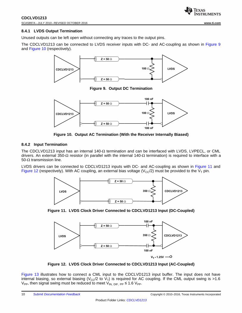
8.4.1 LVDS Output TerminationUnused outputs can be left open without connecting any traces to the output pins.
The CDCLVD1213 can be connected to LVDS receiver inputs with DC- and AC-coupling as shown in Figure 9and Figure 10 (respectively).
Figure 9. Output DC Termination
Figure 10. Output AC Termination (With the Receiver Internally Biased)
8.4.2 Input TerminationThe CDCLVD1213 input has an internal 140-Ω termination and can be interfaced with LVDS, LVPECL, or CMLdrivers. An external 350-Ω resistor (in parallel with the internal 140-Ω termination) is required to interface with a50-Ω transmission line.
LVDS drivers can be connected to CDCLVD1213 inputs with DC- and AC-coupling as shown in Figure 11 andFigure 12 (respectively). With AC coupling, an external bias voltage (VCC/2) must be provided to the VT pin.
Figure 11. LVDS Clock Driver Connected to CDCLVD1213 Input (DC-Coupled)
Figure 12. LVDS Clock Driver Connected to CDCLVD1213 Input (AC-Coupled)
Figure 13 illustrates how to connect a CML input to the CDCLVD1213 input buffer. The input does not haveinternal biasing, so external biasing (VCC/2 to VT) is required for AC coupling. If the CML output swing is >1.6VPP, then signal swing must be reduced to meet VIN, DIF, PP ≤ 1.6 VPP.

150 W VT
= 1.25V
75 W
CDCLVD1213
Z = 50 W
LVPECL
100 nF
Z = 50 W
100 nF75 W
150 W
350 W
VT
= 1.25V
100 nF
CDCLVD1213
Z = 50 W
CML
Z = 50 W
100 nF
350 W
11
CDCLVD1213www.ti.com SCAS897A –JULY 2010–REVISED OCTOBER 2016
Product Folder Links: CDCLVD1213
Submit Documentation FeedbackCopyright © 2010–2016, Texas Instruments Incorporated
Figure 13. CML Clock Driver Connected to CDCLVD1213 Input
Figure 14 illustrates how to connect an LVPECL input to the CDCLVD1213 input buffer. The input does not haveinternal biasing, so external biasing (VCC/2 to VT) is required for AC coupling. The series resistors are required toreduce the LVPECL signal swing if the signal swing is >1.6 Vpp.
Figure 14. LVPECL Clock Driver Connected to CDCLVD1213 Input

2.5 V
INP
INN
156.25 MHz LVDSFrom Backplane 350
PHY
ASIC
VT
DIV
2.5 V
1k
1k
FPGA
CPU
100
100
100
100
Copyright © 2016, Texas Instruments Incorporated
100
12
CDCLVD1213SCAS897A –JULY 2010–REVISED OCTOBER 2016 www.ti.com
Product Folder Links: CDCLVD1213
Submit Documentation Feedback Copyright © 2010–2016, Texas Instruments Incorporated
9 Application and Implementation
NOTEInformation in the following applications sections is not part of the TI componentspecification, and TI does not warrant its accuracy or completeness. TI’s customers areresponsible for determining suitability of components for their purposes. Customers shouldvalidate and test their design implementation to confirm system functionality.
9.1 Application InformationThe CDCLVD1213 is a low additive jitter universal to LVDS fan-out buffer with an integrated frequency divider onone output. The small package, low output skew, and low additive jitter make for a flexible device in demandingapplications.
9.2 Typical Application
Figure 15. Fan-Out Buffer for Line Card Application

13
CDCLVD1213www.ti.com SCAS897A –JULY 2010–REVISED OCTOBER 2016
Product Folder Links: CDCLVD1213
Submit Documentation FeedbackCopyright © 2010–2016, Texas Instruments Incorporated
Typical Application (continued)9.2.1 Design RequirementsThe CDCLVD1213 shown in Figure 15 is configured with a 156.25-MHz LVDS clock from the backplane as itsinput frequency. The LVDS clock is AC-coupled. A resistor divider (and a 0.1-µF capacitor to reduce noise) isused to set the bias voltage correctly at the VT pin. The configuration example is driving 4 LVDS receivers in aline card application with the following properties:• The PHY device is capable of DC-coupling with an LVDS driver such as the CDCLVD1213. This PHY device
features internal termination so no additional components are required for proper operation.• The ASIC LVDS receiver features internal termination and operates at the same common-mode voltage as
the CDCLVD1213. Again, no additional components are required.• The FPGA requires external AC-coupling, but has internal termination. 0.1-µF capacitors are placed to
provide AC-coupling.• The CPU on output QD is internally terminated, and requires only external AC-coupling capacitors. The DIV
pin is pulled to ground with a 100-Ω resistor to set the frequency divider to 1 so that the CPU clock frequencyis also 156.25 MHz.
9.2.2 Detailed Design ProcedureSee Input Termination for proper input terminations, dependent on single-ended or differential inputs.
See LVDS Output Termination for output termination schemes depending on the receiver application.
Unused outputs can be left floating.
In this example, the PHY, ASIC, and FPGA or CPU require different schemes. Power supply filtering andbypassing is critical for low-noise applications.
See Power Supply Recommendations for recommended filtering techniques. A reference layout is provided inLow-Additive Jitter, Four-LVDS-Outputs Clock Buffer With Divider EVM (SCAU044).
9.2.3 Application CurvesThe CDCLVD12xx's low additive noise is shown in this line card application. The low noise 156.25-MHz sourcewith 67-fs RMS jitter drives the CDCLVD12xx, resulting in 80-fs RMS when integrated from 12 kHz to 20 MHz.The resultant additive jitter is a low 44-fs RMS for this configuration.
Reference signal is low-noise Rohde and Schwarz SMA100A
Figure 16. CDCLVD12xx Reference Phase Noise,67-fs RMS (12 kHz to 20 MHz)
Figure 17. CDCLVD12xx Output Phase Noise,80-fs RMS (12 kHz to 20 MHz)
Ferrite Bead
1 µF 10 µF 0.1 µF
14
CDCLVD1213SCAS897A –JULY 2010–REVISED OCTOBER 2016 www.ti.com
Product Folder Links: CDCLVD1213
Submit Documentation Feedback Copyright © 2010–2016, Texas Instruments Incorporated
10 Power Supply RecommendationsHigh-performance clock buffers are sensitive to noise on the power supply, which can dramatically increase theadditive jitter of the buffer. Thus, it is essential to reduce noise from the system power supply, especially whenjitter or phase noise is critical to applications.
Filter capacitors are used to eliminate the low-frequency noise from the power supply, where the bypasscapacitors provide the low impedance path for high-frequency noise and guard the power-supply system againstthe induced fluctuations. These bypass capacitors also provide instantaneous current surges as required by thedevice and must have low equivalent series resistance (ESR). To properly use the bypass capacitors, they mustbe placed close to the power-supply pins and laid out with short loops to minimize inductance. TI recommendsadding as many high-frequency (for example, 0.1-µF) bypass capacitors as there are supply pins in the package.TI recommends, but does not require, inserting a ferrite bead between the board power supply and the chippower supply that isolates the high-frequency switching noises generated by the clock driver; these beadsprevent the switching noise from leaking into the board supply. Choose an appropriate ferrite bead with low DC-resistance because it is imperative to provide adequate isolation between the board supply and the chip supply,as well as to maintain a voltage at the supply pins that is greater than the minimum voltage required for properoperation.
Figure 18 shows this recommended power-supply decoupling method.
Figure 18. Power-Supply Decoupling

15
CDCLVD1213www.ti.com SCAS897A –JULY 2010–REVISED OCTOBER 2016
Product Folder Links: CDCLVD1213
Submit Documentation FeedbackCopyright © 2010–2016, Texas Instruments Incorporated
11 Layout
11.1 Layout GuidelinesFor reliability and performance reasons, the die temperature must be limited to a maximum of 125°C.
The device package has an exposed pad that provides the primary heat removal path to the printed-circuit board(PCB). To maximize the heat dissipation from the package, a thermal landing pattern including multiple vias to aground plane must be incorporated into the PCB within the footprint of the package. The thermal pad must besoldered down to ensure adequate heat conduction to of the package. Figure 19 shows a recommended landand via pattern.
11.2 Layout Example
Figure 19. Recommended PCB Layout
11.3 Thermal ConsiderationsThe CDCLVD1213 supports high temperatures on the printed-circuit board (PCB) measured at the thermal pad.The system designer must ensure that the maximum junction temperature is not exceeded. ΨJB can allow thesystem designer to measure the board temperature with a fine gauge thermocouple and back calculate thejunction temperature using Equation 1. Note that ΨJB is close to RθJB as 75% to 95% of a device's heat isdissipated by the PCB.
TJ = TPCB + ( ΨJB × Power) (1)
Example:Calculation of the junction-lead temperature with a 4-layer JEDEC test board using four thermal vias:
TPCB = 105°CΨJB = 19.4°C/WPowerinclTerm = Imax × Vmax = 85 mA × 2.625 V = 223 mW (maximum power consumption includingtermination resistors)PowerexclTerm = 215 mW (maximum power consumption excluding termination resistors, see PowerConsumption of LVPECL and LVDS (SLYT127) for further details)ΔTJ = ΨJB × PowerexclTerm = 19.4°C/W × 215 mW = 4.17°CTJ = ΔTJ + TChassis = 4.17°C + 105°C = 109.17°C (maximum junction temperature of 125°C is notviolated)
Further information can be found at Semiconductor and IC Package Thermal Metrics (SPRA953) and UsingThermal Calculation Tools for Analog Components (SLUA566).

16
CDCLVD1213SCAS897A –JULY 2010–REVISED OCTOBER 2016 www.ti.com
Product Folder Links: CDCLVD1213
Submit Documentation Feedback Copyright © 2010–2016, Texas Instruments Incorporated
12 Device and Documentation Support
12.1 Documentation Support
12.1.1 Related DocumentationFor related documentation see the following:• Low-Additive Jitter, Four-LVDS-Outputs Clock Buffer With Divider EVM (SCAU044)• Power Consumption of LVPECL and LVDS (SLYT127)• Semiconductor and IC Package Thermal Metrics (SPRA953)• Using Thermal Calculation Tools for Analog Components (SLUA566)
12.2 Receiving Notification of Documentation UpdatesTo receive notification of documentation updates, navigate to the device product folder on ti.com. In the upperright corner, click on Alert me to register and receive a weekly digest of any product information that haschanged. For change details, review the revision history included in any revised document.
12.3 Community ResourcesThe following links connect to TI community resources. Linked contents are provided "AS IS" by the respectivecontributors. They do not constitute TI specifications and do not necessarily reflect TI's views; see TI's Terms ofUse.
TI E2E™ Online Community TI's Engineer-to-Engineer (E2E) Community. Created to foster collaborationamong engineers. At e2e.ti.com, you can ask questions, share knowledge, explore ideas and helpsolve problems with fellow engineers.
Design Support TI's Design Support Quickly find helpful E2E forums along with design support tools andcontact information for technical support.
12.4 TrademarksE2E is a trademark of Texas Instruments.
12.5 Electrostatic Discharge CautionThese devices have limited built-in ESD protection. The leads should be shorted together or the device placed in conductive foamduring storage or handling to prevent electrostatic damage to the MOS gates.
12.6 GlossarySLYZ022 — TI Glossary.
This glossary lists and explains terms, acronyms, and definitions.
13 Mechanical, Packaging, and Orderable InformationThe following pages include mechanical, packaging, and orderable information. This information is the mostcurrent data available for the designated devices. This data is subject to change without notice and revision ofthis document. For browser-based versions of this data sheet, refer to the left-hand navigation.

PACKAGE OPTION ADDENDUM
www.ti.com 11-Aug-2017
Addendum-Page 1
PACKAGING INFORMATION
Orderable Device Status(1)
Package Type PackageDrawing
Pins PackageQty
Eco Plan(2)
Lead/Ball Finish(6)
MSL Peak Temp(3)
Op Temp (°C) Device Marking(4/5)
Samples
CDCLVD1213RGTR ACTIVE VQFN RGT 16 3000 Green (RoHS& no Sb/Br)
CU NIPDAU Level-2-260C-1 YEAR -40 to 85 D1213
CDCLVD1213RGTT ACTIVE VQFN RGT 16 250 Green (RoHS& no Sb/Br)
CU NIPDAU Level-2-260C-1 YEAR -40 to 85 D1213
(1) The marketing status values are defined as follows:ACTIVE: Product device recommended for new designs.LIFEBUY: TI has announced that the device will be discontinued, and a lifetime-buy period is in effect.NRND: Not recommended for new designs. Device is in production to support existing customers, but TI does not recommend using this part in a new design.PREVIEW: Device has been announced but is not in production. Samples may or may not be available.OBSOLETE: TI has discontinued the production of the device.
(2) RoHS: TI defines "RoHS" to mean semiconductor products that are compliant with the current EU RoHS requirements for all 10 RoHS substances, including the requirement that RoHS substancedo not exceed 0.1% by weight in homogeneous materials. Where designed to be soldered at high temperatures, "RoHS" products are suitable for use in specified lead-free processes. TI mayreference these types of products as "Pb-Free".RoHS Exempt: TI defines "RoHS Exempt" to mean products that contain lead but are compliant with EU RoHS pursuant to a specific EU RoHS exemption.Green: TI defines "Green" to mean the content of Chlorine (Cl) and Bromine (Br) based flame retardants meet JS709B low halogen requirements of <=1000ppm threshold. Antimony trioxide basedflame retardants must also meet the <=1000ppm threshold requirement.
(3) MSL, Peak Temp. - The Moisture Sensitivity Level rating according to the JEDEC industry standard classifications, and peak solder temperature.
(4) There may be additional marking, which relates to the logo, the lot trace code information, or the environmental category on the device.
(5) Multiple Device Markings will be inside parentheses. Only one Device Marking contained in parentheses and separated by a "~" will appear on a device. If a line is indented then it is a continuationof the previous line and the two combined represent the entire Device Marking for that device.
(6) Lead/Ball Finish - Orderable Devices may have multiple material finish options. Finish options are separated by a vertical ruled line. Lead/Ball Finish values may wrap to two lines if the finishvalue exceeds the maximum column width.
Important Information and Disclaimer:The information provided on this page represents TI's knowledge and belief as of the date that it is provided. TI bases its knowledge and belief on informationprovided by third parties, and makes no representation or warranty as to the accuracy of such information. Efforts are underway to better integrate information from third parties. TI has taken andcontinues to take reasonable steps to provide representative and accurate information but may not have conducted destructive testing or chemical analysis on incoming materials and chemicals.TI and TI suppliers consider certain information to be proprietary, and thus CAS numbers and other limited information may not be available for release.
In no event shall TI's liability arising out of such information exceed the total purchase price of the TI part(s) at issue in this document sold by TI to Customer on an annual basis.

PACKAGE OPTION ADDENDUM
www.ti.com 11-Aug-2017
Addendum-Page 2

TAPE AND REEL INFORMATION
*All dimensions are nominal
Device PackageType
PackageDrawing
Pins SPQ ReelDiameter
(mm)
ReelWidth
W1 (mm)
A0(mm)
B0(mm)
K0(mm)
P1(mm)
W(mm)
Pin1Quadrant
CDCLVD1213RGTR VQFN RGT 16 3000 330.0 12.4 3.3 3.3 1.1 8.0 12.0 Q2
CDCLVD1213RGTT VQFN RGT 16 250 180.0 12.4 3.3 3.3 1.1 8.0 12.0 Q2
PACKAGE MATERIALS INFORMATION
www.ti.com 11-Aug-2017
Pack Materials-Page 1

*All dimensions are nominal
Device Package Type Package Drawing Pins SPQ Length (mm) Width (mm) Height (mm)
CDCLVD1213RGTR VQFN RGT 16 3000 336.6 336.6 28.6
CDCLVD1213RGTT VQFN RGT 16 250 210.0 185.0 35.0
PACKAGE MATERIALS INFORMATION
www.ti.com 11-Aug-2017
Pack Materials-Page 2

www.ti.com
PACKAGE OUTLINE
C
16X 0.300.18
1.68 0.07
16X 0.50.3
1 MAX
(0.2) TYP
0.050.00
12X 0.5
4X1.5
A 3.12.9
B
3.12.9
VQFN - 1 mm max heightRGT0016CPLASTIC QUAD FLATPACK - NO LEAD
4222419/B 11/2016
PIN 1 INDEX AREA
0.08
SEATING PLANE
1
49
12
5 8
16 13
(OPTIONAL)PIN 1 ID 0.1 C A B
0.05
EXPOSEDTHERMAL PAD
SYMM
SYMM
NOTES: 1. All linear dimensions are in millimeters. Any dimensions in parenthesis are for reference only. Dimensioning and tolerancing per ASME Y14.5M. 2. This drawing is subject to change without notice. 3. The package thermal pad must be soldered to the printed circuit board for thermal and mechanical performance.
SCALE 3.600

www.ti.com
EXAMPLE BOARD LAYOUT
0.07 MINALL AROUND
0.07 MAXALL AROUND
16X (0.24)
16X (0.6)
( 0.2) TYPVIA
12X (0.5)
(2.8)
(2.8)
(0.58)TYP
( 1.68)
(R0.05)ALL PAD CORNERS
(0.58) TYP
VQFN - 1 mm max heightRGT0016CPLASTIC QUAD FLATPACK - NO LEAD
4222419/B 11/2016
SYMM
1
4
5 8
9
12
1316
SYMM
LAND PATTERN EXAMPLESCALE:20X
NOTES: (continued) 4. This package is designed to be soldered to a thermal pad on the board. For more information, see Texas Instruments literature number SLUA271 (www.ti.com/lit/slua271).5. Vias are optional depending on application, refer to device data sheet. If any vias are implemented, refer to their locations shown on this view. It is recommended that vias under paste be filled, plugged or tented.
SOLDER MASKOPENING
METAL UNDERSOLDER MASK
SOLDER MASKDEFINED
METAL
SOLDER MASKOPENING
SOLDER MASK DETAILS
NON SOLDER MASKDEFINED
(PREFERRED)

www.ti.com
EXAMPLE STENCIL DESIGN
16X (0.6)
16X (0.24)
12X (0.5)
(2.8)
(2.8)
( 1.55)
(R0.05) TYP
VQFN - 1 mm max heightRGT0016CPLASTIC QUAD FLATPACK - NO LEAD
4222419/B 11/2016
NOTES: (continued) 6. Laser cutting apertures with trapezoidal walls and rounded corners may offer better paste release. IPC-7525 may have alternate design recommendations.
SYMM
ALL AROUNDMETAL
SOLDER PASTE EXAMPLEBASED ON 0.125 mm THICK STENCIL
EXPOSED PAD 17:
85% PRINTED SOLDER COVERAGE BY AREA UNDER PACKAGESCALE:25X
SYMM
1
4
5 8
9
12
1316
17

IMPORTANT NOTICE
Texas Instruments Incorporated (TI) reserves the right to make corrections, enhancements, improvements and other changes to itssemiconductor products and services per JESD46, latest issue, and to discontinue any product or service per JESD48, latest issue. Buyersshould obtain the latest relevant information before placing orders and should verify that such information is current and complete.TI’s published terms of sale for semiconductor products (http://www.ti.com/sc/docs/stdterms.htm) apply to the sale of packaged integratedcircuit products that TI has qualified and released to market. Additional terms may apply to the use or sale of other types of TI products andservices.Reproduction of significant portions of TI information in TI data sheets is permissible only if reproduction is without alteration and isaccompanied by all associated warranties, conditions, limitations, and notices. TI is not responsible or liable for such reproduceddocumentation. Information of third parties may be subject to additional restrictions. Resale of TI products or services with statementsdifferent from or beyond the parameters stated by TI for that product or service voids all express and any implied warranties for theassociated TI product or service and is an unfair and deceptive business practice. TI is not responsible or liable for any such statements.Buyers and others who are developing systems that incorporate TI products (collectively, “Designers”) understand and agree that Designersremain responsible for using their independent analysis, evaluation and judgment in designing their applications and that Designers havefull and exclusive responsibility to assure the safety of Designers' applications and compliance of their applications (and of all TI productsused in or for Designers’ applications) with all applicable regulations, laws and other applicable requirements. Designer represents that, withrespect to their applications, Designer has all the necessary expertise to create and implement safeguards that (1) anticipate dangerousconsequences of failures, (2) monitor failures and their consequences, and (3) lessen the likelihood of failures that might cause harm andtake appropriate actions. Designer agrees that prior to using or distributing any applications that include TI products, Designer willthoroughly test such applications and the functionality of such TI products as used in such applications.TI’s provision of technical, application or other design advice, quality characterization, reliability data or other services or information,including, but not limited to, reference designs and materials relating to evaluation modules, (collectively, “TI Resources”) are intended toassist designers who are developing applications that incorporate TI products; by downloading, accessing or using TI Resources in anyway, Designer (individually or, if Designer is acting on behalf of a company, Designer’s company) agrees to use any particular TI Resourcesolely for this purpose and subject to the terms of this Notice.TI’s provision of TI Resources does not expand or otherwise alter TI’s applicable published warranties or warranty disclaimers for TIproducts, and no additional obligations or liabilities arise from TI providing such TI Resources. TI reserves the right to make corrections,enhancements, improvements and other changes to its TI Resources. TI has not conducted any testing other than that specificallydescribed in the published documentation for a particular TI Resource.Designer is authorized to use, copy and modify any individual TI Resource only in connection with the development of applications thatinclude the TI product(s) identified in such TI Resource. NO OTHER LICENSE, EXPRESS OR IMPLIED, BY ESTOPPEL OR OTHERWISETO ANY OTHER TI INTELLECTUAL PROPERTY RIGHT, AND NO LICENSE TO ANY TECHNOLOGY OR INTELLECTUAL PROPERTYRIGHT OF TI OR ANY THIRD PARTY IS GRANTED HEREIN, including but not limited to any patent right, copyright, mask work right, orother intellectual property right relating to any combination, machine, or process in which TI products or services are used. Informationregarding or referencing third-party products or services does not constitute a license to use such products or services, or a warranty orendorsement thereof. Use of TI Resources may require a license from a third party under the patents or other intellectual property of thethird party, or a license from TI under the patents or other intellectual property of TI.TI RESOURCES ARE PROVIDED “AS IS” AND WITH ALL FAULTS. TI DISCLAIMS ALL OTHER WARRANTIES ORREPRESENTATIONS, EXPRESS OR IMPLIED, REGARDING RESOURCES OR USE THEREOF, INCLUDING BUT NOT LIMITED TOACCURACY OR COMPLETENESS, TITLE, ANY EPIDEMIC FAILURE WARRANTY AND ANY IMPLIED WARRANTIES OFMERCHANTABILITY, FITNESS FOR A PARTICULAR PURPOSE, AND NON-INFRINGEMENT OF ANY THIRD PARTY INTELLECTUALPROPERTY RIGHTS. TI SHALL NOT BE LIABLE FOR AND SHALL NOT DEFEND OR INDEMNIFY DESIGNER AGAINST ANY CLAIM,INCLUDING BUT NOT LIMITED TO ANY INFRINGEMENT CLAIM THAT RELATES TO OR IS BASED ON ANY COMBINATION OFPRODUCTS EVEN IF DESCRIBED IN TI RESOURCES OR OTHERWISE. IN NO EVENT SHALL TI BE LIABLE FOR ANY ACTUAL,DIRECT, SPECIAL, COLLATERAL, INDIRECT, PUNITIVE, INCIDENTAL, CONSEQUENTIAL OR EXEMPLARY DAMAGES INCONNECTION WITH OR ARISING OUT OF TI RESOURCES OR USE THEREOF, AND REGARDLESS OF WHETHER TI HAS BEENADVISED OF THE POSSIBILITY OF SUCH DAMAGES.Unless TI has explicitly designated an individual product as meeting the requirements of a particular industry standard (e.g., ISO/TS 16949and ISO 26262), TI is not responsible for any failure to meet such industry standard requirements.Where TI specifically promotes products as facilitating functional safety or as compliant with industry functional safety standards, suchproducts are intended to help enable customers to design and create their own applications that meet applicable functional safety standardsand requirements. Using products in an application does not by itself establish any safety features in the application. Designers mustensure compliance with safety-related requirements and standards applicable to their applications. Designer may not use any TI products inlife-critical medical equipment unless authorized officers of the parties have executed a special contract specifically governing such use.Life-critical medical equipment is medical equipment where failure of such equipment would cause serious bodily injury or death (e.g., lifesupport, pacemakers, defibrillators, heart pumps, neurostimulators, and implantables). Such equipment includes, without limitation, allmedical devices identified by the U.S. Food and Drug Administration as Class III devices and equivalent classifications outside the U.S.TI may expressly designate certain products as completing a particular qualification (e.g., Q100, Military Grade, or Enhanced Product).Designers agree that it has the necessary expertise to select the product with the appropriate qualification designation for their applicationsand that proper product selection is at Designers’ own risk. Designers are solely responsible for compliance with all legal and regulatoryrequirements in connection with such selection.Designer will fully indemnify TI and its representatives against any damages, costs, losses, and/or liabilities arising out of Designer’s non-compliance with the terms and provisions of this Notice.
Mailing Address: Texas Instruments, Post Office Box 655303, Dallas, Texas 75265Copyright © 2017, Texas Instruments Incorporated

Mouser Electronics
Authorized Distributor
Click to View Pricing, Inventory, Delivery & Lifecycle Information: Texas Instruments:
CDCLVD1213RGTR CDCLVD1213RGTT