Embed Size (px)
Citation preview
PE
EQ
VCC
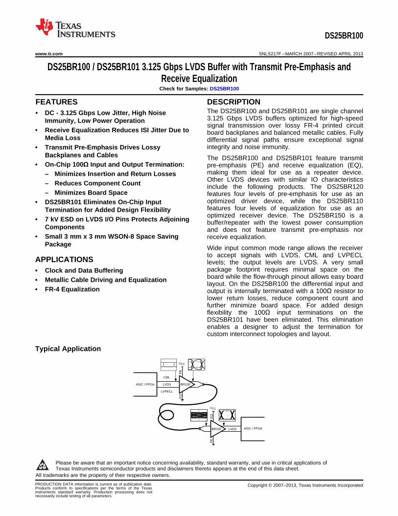
ASIC / FPGA
PE
EQ
VCC
CML
LVDS
LVPECL
ASIC / FPGALVDS
BR100
BR100
DS25BR100
www.ti.com SNLS217F –MARCH 2007–REVISED APRIL 2013
DS25BR100 / DS25BR101 3.125 Gbps LVDS Buffer with Transmit Pre-Emphasis andReceive Equalization
Check for Samples: DS25BR100
1FEATURES DESCRIPTIONThe DS25BR100 and DS25BR101 are single channel
2• DC - 3.125 Gbps Low Jitter, High Noise3.125 Gbps LVDS buffers optimized for high-speedImmunity, Low Power Operationsignal transmission over lossy FR-4 printed circuit
• Receive Equalization Reduces ISI Jitter Due to board backplanes and balanced metallic cables. FullyMedia Loss differential signal paths ensure exceptional signal
integrity and noise immunity.• Transmit Pre-Emphasis Drives LossyBackplanes and Cables The DS25BR100 and DS25BR101 feature transmit
• On-Chip 100Ω Input and Output Termination: pre-emphasis (PE) and receive equalization (EQ),making them ideal for use as a repeater device.– Minimizes Insertion and Return LossesOther LVDS devices with similar IO characteristics– Reduces Component Count include the following products. The DS25BR120
– Minimizes Board Space features four levels of pre-emphasis for use as anoptimized driver device, while the DS25BR110• DS25BR101 Eliminates On-Chip Inputfeatures four levels of equalization for use as anTermination for Added Design Flexibilityoptimized receiver device. The DS25BR150 is a
• 7 kV ESD on LVDS I/O Pins Protects Adjoining buffer/repeater with the lowest power consumptionComponents and does not feature transmit pre-emphasis nor
• Small 3 mm x 3 mm WSON-8 Space Saving receive equalization.Package Wide input common mode range allows the receiver
to accept signals with LVDS, CML and LVPECLAPPLICATIONS levels; the output levels are LVDS. A very small
package footprint requires minimal space on the• Clock and Data Bufferingboard while the flow-through pinout allows easy board• Metallic Cable Driving and Equalizationlayout. On the DS25BR100 the differential input and
• FR-4 Equalization output is internally terminated with a 100Ω resistor tolower return losses, reduce component count andfurther minimize board space. For added designflexibility the 100Ω input terminations on theDS25BR101 have been eliminated. This eliminationenables a designer to adjust the termination forcustom interconnect topologies and layout.
Typical Application
1
Please be aware that an important notice concerning availability, standard warranty, and use in critical applications ofTexas Instruments semiconductor products and disclaimers thereto appears at the end of this data sheet.
2All trademarks are the property of their respective owners.
PRODUCTION DATA information is current as of publication date. Copyright © 2007–2013, Texas Instruments IncorporatedProducts conform to specifications per the terms of the TexasInstruments standard warranty. Production processing does notnecessarily include testing of all parameters.
EQ
IN+
IN-
PE
VCC
OUT+
OUT-
NC
1
2
3
4
8
6
5
7
GND
DAP
PE
OUT+
OUT-
EQ
IN+
IN-
DS25BR100
SNLS217F –MARCH 2007–REVISED APRIL 2013 www.ti.com
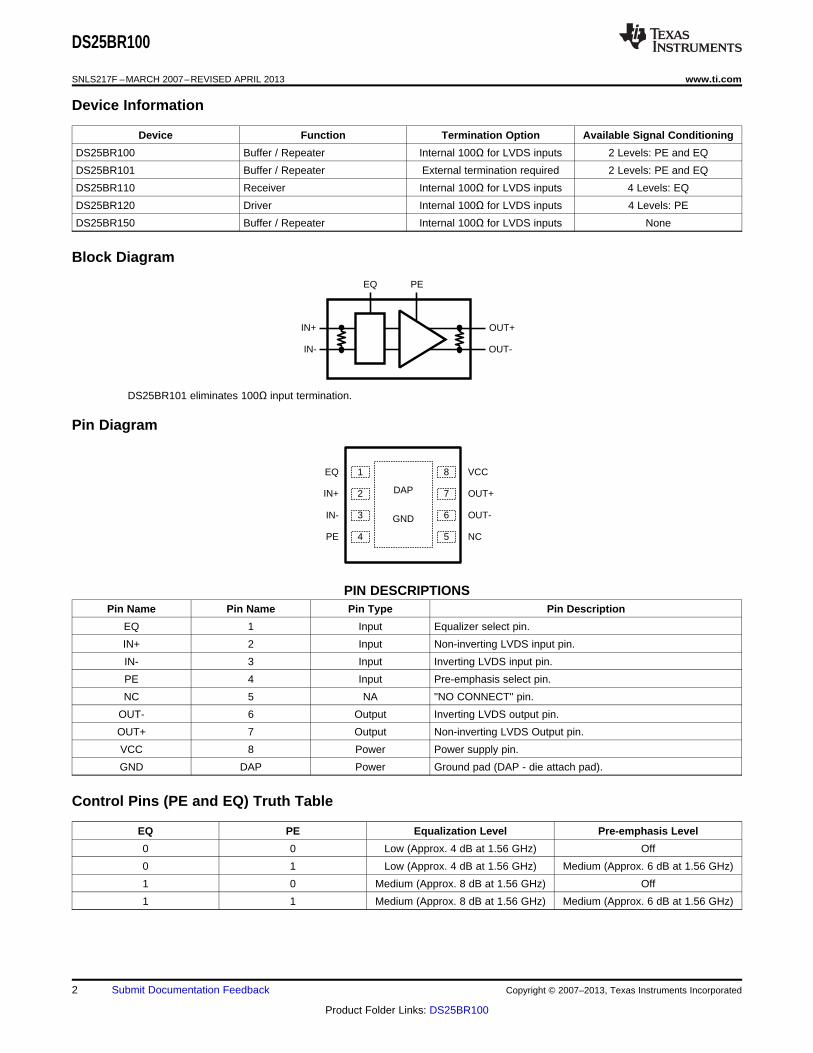
Device Information
Device Function Termination Option Available Signal Conditioning
DS25BR100 Buffer / Repeater Internal 100Ω for LVDS inputs 2 Levels: PE and EQ
DS25BR101 Buffer / Repeater External termination required 2 Levels: PE and EQ
DS25BR110 Receiver Internal 100Ω for LVDS inputs 4 Levels: EQ
DS25BR120 Driver Internal 100Ω for LVDS inputs 4 Levels: PE
DS25BR150 Buffer / Repeater Internal 100Ω for LVDS inputs None
Block Diagram
DS25BR101 eliminates 100Ω input termination.
Pin Diagram
PIN DESCRIPTIONSPin Name Pin Name Pin Type Pin Description
EQ 1 Input Equalizer select pin.
IN+ 2 Input Non-inverting LVDS input pin.
IN- 3 Input Inverting LVDS input pin.
PE 4 Input Pre-emphasis select pin.
NC 5 NA "NO CONNECT" pin.
OUT- 6 Output Inverting LVDS output pin.
OUT+ 7 Output Non-inverting LVDS Output pin.
VCC 8 Power Power supply pin.
GND DAP Power Ground pad (DAP - die attach pad).
Control Pins (PE and EQ) Truth Table
EQ PE Equalization Level Pre-emphasis Level
0 0 Low (Approx. 4 dB at 1.56 GHz) Off
0 1 Low (Approx. 4 dB at 1.56 GHz) Medium (Approx. 6 dB at 1.56 GHz)
1 0 Medium (Approx. 8 dB at 1.56 GHz) Off
1 1 Medium (Approx. 8 dB at 1.56 GHz) Medium (Approx. 6 dB at 1.56 GHz)
2 Submit Documentation Feedback Copyright © 2007–2013, Texas Instruments Incorporated
Product Folder Links: DS25BR100
DS25BR100
www.ti.com SNLS217F –MARCH 2007–REVISED APRIL 2013
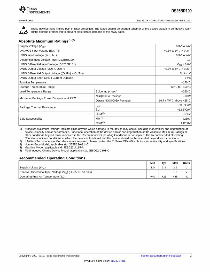
These devices have limited built-in ESD protection. The leads should be shorted together or the device placed in conductive foamduring storage or handling to prevent electrostatic damage to the MOS gates.
Absolute Maximum Ratings (1) (2)
Supply Voltage (VCC) −0.3V to +4V
LVCMOS Input Voltage (EQ, PE) −0.3V to (VCC + 0.3V)
LVDS Input Voltage (IN+, IN−) −0.3V to +4V
Differential Input Voltage |VID| (DS25BR100) 1V
LVDS Differential Input Voltage (DS25BR101) VCC + 0.6V
LVDS Output Voltage (OUT+, OUT−) −0.3V to (VCC + 0.3V)
LVDS Differential Output Voltage ((OUT+) - (OUT−)) 0V to 1V
LVDS Output Short Circuit Current Duration 5 ms
Junction Temperature +150°C
Storage Temperature Range −65°C to +150°C
Lead Temperature Range Soldering (4 sec.) +260°C
NGQ0008A Package 2.08WMaximum Package Power Dissipation at 25°C
Derate NGQ0008A Package 16.7 mW/°C above +25°C
θJA +60.0°C/WPackage Thermal Resistance
θJC +12.3°C/W
HBM (3) ≥7 kV
ESD Susceptibility MM (4) ≥250V
CDM (5) ≥1250V
(1) “Absolute Maximum Ratings” indicate limits beyond which damage to the device may occur, including inoperability and degradation ofdevice reliability and/or performance. Functional operation of the device and/or non-degradation at the Absolute Maximum Ratings orother conditions beyond those indicated in the Recommended Operating Conditions is not implied. The Recommended OperatingConditions indicate conditions at which the device is functional and the device should not be operated beyond such conditions.
(2) If Military/Aerospace specified devices are required, please contact the TI Sales Office/Distributors for availability and specifications.(3) Human Body Model, applicable std. JESD22-A114C(4) Machine Model, applicable std. JESD22-A115-A(5) Field Induced Charge Device Model, applicable std. JESD22-C101-C
Recommended Operating ConditionsMin Typ Max Units
Supply Voltage (VCC) 3.0 3.3 3.6 V
Receiver Differential Input Voltage (VID) (DS25BR100 only) 1.0 V
Operating Free Air Temperature (TA) −40 +25 +85 °C
Copyright © 2007–2013, Texas Instruments Incorporated Submit Documentation Feedback 3
Product Folder Links: DS25BR100
DS25BR100
SNLS217F –MARCH 2007–REVISED APRIL 2013 www.ti.com
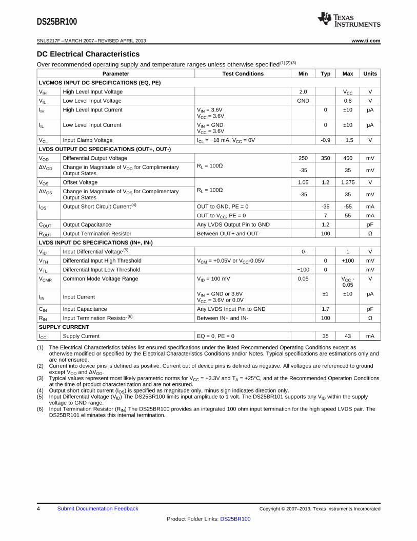
DC Electrical CharacteristicsOver recommended operating supply and temperature ranges unless otherwise specified (1) (2) (3)
Parameter Test Conditions Min Typ Max Units
LVCMOS INPUT DC SPECIFICATIONS (EQ, PE)
VIH High Level Input Voltage 2.0 VCC V
VIL Low Level Input Voltage GND 0.8 V
IIH High Level Input Current VIN = 3.6V 0 ±10 μAVCC = 3.6V
IIL Low Level Input Current VIN = GND 0 ±10 μAVCC = 3.6V
VCL Input Clamp Voltage ICL = −18 mA, VCC = 0V -0.9 −1.5 V
LVDS OUTPUT DC SPECIFICATIONS (OUT+, OUT-)
VOD Differential Output Voltage 250 350 450 mVRL = 100ΩΔVOD Change in Magnitude of VOD for Complimentary -35 35 mVOutput States
VOS Offset Voltage 1.05 1.2 1.375 VRL = 100ΩΔVOS Change in Magnitude of VOS for Complimentary -35 35 mVOutput States
IOS Output Short Circuit Current (4) OUT to GND, PE = 0 -35 -55 mA
OUT to VCC, PE = 0 7 55 mA
COUT Output Capacitance Any LVDS Output Pin to GND 1.2 pF
ROUT Output Termination Resistor Between OUT+ and OUT- 100 ΩLVDS INPUT DC SPECIFICATIONS (IN+, IN-)
VID Input Differential Voltage (5) 0 1 V
VTH Differential Input High Threshold VCM = +0.05V or VCC-0.05V 0 +100 mV
VTL Differential Input Low Threshold −100 0 mV
VCMR Common Mode Voltage Range VID = 100 mV 0.05 VCC - V0.05
VIN = GND or 3.6V ±1 ±10 μAIIN Input Current VCC = 3.6V or 0.0V
CIN Input Capacitance Any LVDS Input Pin to GND 1.7 pF
RIN Input Termination Resistor (6) Between IN+ and IN- 100 ΩSUPPLY CURRENT
ICC Supply Current EQ = 0, PE = 0 35 43 mA
(1) The Electrical Characteristics tables list ensured specifications under the listed Recommended Operating Conditions except asotherwise modified or specified by the Electrical Characteristics Conditions and/or Notes. Typical specifications are estimations only andare not ensured.
(2) Current into device pins is defined as positive. Current out of device pins is defined as negative. All voltages are referenced to groundexcept VOD and ΔVOD.
(3) Typical values represent most likely parametric norms for VCC = +3.3V and TA = +25°C, and at the Recommended Operation Conditionsat the time of product characterization and are not ensured.
(4) Output short circuit current (IOS) is specified as magnitude only, minus sign indicates direction only.(5) Input Differential Voltage (VID) The DS25BR100 limits input amplitude to 1 volt. The DS25BR101 supports any VID within the supply
voltage to GND range.(6) Input Termination Resistor (RIN) The DS25BR100 provides an integrated 100 ohm input termination for the high speed LVDS pair. The
DS25BR101 eliminates this internal termination.
4 Submit Documentation Feedback Copyright © 2007–2013, Texas Instruments Incorporated
Product Folder Links: DS25BR100
DS25BR100
www.ti.com SNLS217F –MARCH 2007–REVISED APRIL 2013
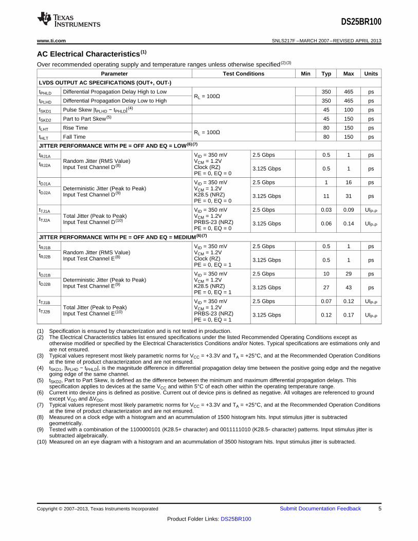
AC Electrical Characteristics (1)
Over recommended operating supply and temperature ranges unless otherwise specified (2) (3)
Parameter Test Conditions Min Typ Max Units
LVDS OUTPUT AC SPECIFICATIONS (OUT+, OUT-)
tPHLD Differential Propagation Delay High to Low 350 465 psRL = 100Ω
tPLHD Differential Propagation Delay Low to High 350 465 ps
tSKD1 Pulse Skew |tPLHD − tPHLD| (4) 45 100 ps
tSKD2 Part to Part Skew (5) 45 150 ps
tLHT Rise Time 80 150 psRL = 100Ω
tHLT Fall Time 80 150 ps
JITTER PERFORMANCE WITH PE = OFF AND EQ = LOW (6) (7)
tRJ1A VID = 350 mV 2.5 Gbps 0.5 1 psRandom Jitter (RMS Value) VCM = 1.2VtRJ2A Input Test Channel D (8) Clock (RZ) 3.125 Gbps 0.5 1 ps
PE = 0, EQ = 0
tDJ1A VID = 350 mV 2.5 Gbps 1 16 psDeterministic Jitter (Peak to Peak) VCM = 1.2VtDJ2A Input Test Channel D (9) K28.5 (NRZ) 3.125 Gbps 11 31 ps
PE = 0, EQ = 0
tTJ1A VID = 350 mV 2.5 Gbps 0.03 0.09 UIP-PTotal Jitter (Peak to Peak) VCM = 1.2VtTJ2A Input Test Channel D (10) PRBS-23 (NRZ) 3.125 Gbps 0.06 0.14 UIP-P
PE = 0, EQ = 0
JITTER PERFORMANCE WITH PE = OFF AND EQ = MEDIUM (6) (7)
tRJ1B VID = 350 mV 2.5 Gbps 0.5 1 psRandom Jitter (RMS Value) VCM = 1.2VtRJ2B Input Test Channel E (8) Clock (RZ) 3.125 Gbps 0.5 1 ps
PE = 0, EQ = 1
tDJ1B VID = 350 mV 2.5 Gbps 10 29 psDeterministic Jitter (Peak to Peak) VCM = 1.2VtDJ2B Input Test Channel E (9) K28.5 (NRZ) 3.125 Gbps 27 43 ps
PE = 0, EQ = 1
tTJ1B VID = 350 mV 2.5 Gbps 0.07 0.12 UIP-PTotal Jitter (Peak to Peak) VCM = 1.2VtTJ2B Input Test Channel E (10) PRBS-23 (NRZ) 3.125 Gbps 0.12 0.17 UIP-P
PE = 0, EQ = 1
(1) Specification is ensured by characterization and is not tested in production.(2) The Electrical Characteristics tables list ensured specifications under the listed Recommended Operating Conditions except as
otherwise modified or specified by the Electrical Characteristics Conditions and/or Notes. Typical specifications are estimations only andare not ensured.
(3) Typical values represent most likely parametric norms for VCC = +3.3V and TA = +25°C, and at the Recommended Operation Conditionsat the time of product characterization and are not ensured.
(4) tSKD1, |tPLHD − tPHLD|, is the magnitude difference in differential propagation delay time between the positive going edge and the negativegoing edge of the same channel.
(5) tSKD2, Part to Part Skew, is defined as the difference between the minimum and maximum differential propagation delays. Thisspecification applies to devices at the same VCC and within 5°C of each other within the operating temperature range.
(6) Current into device pins is defined as positive. Current out of device pins is defined as negative. All voltages are referenced to groundexcept VOD and ΔVOD.
(7) Typical values represent most likely parametric norms for VCC = +3.3V and TA = +25°C, and at the Recommended Operation Conditionsat the time of product characterization and are not ensured.
(8) Measured on a clock edge with a histogram and an acummulation of 1500 histogram hits. Input stimulus jitter is subtractedgeometrically.
(9) Tested with a combination of the 1100000101 (K28.5+ character) and 0011111010 (K28.5- character) patterns. Input stimulus jitter issubtracted algebraically.
(10) Measured on an eye diagram with a histogram and an acummulation of 3500 histogram hits. Input stimulus jitter is subtracted.
Copyright © 2007–2013, Texas Instruments Incorporated Submit Documentation Feedback 5
Product Folder Links: DS25BR100
DS25BR100
SNLS217F –MARCH 2007–REVISED APRIL 2013 www.ti.com
AC Electrical Characteristics(1) (continued)Over recommended operating supply and temperature ranges unless otherwise specified(2)(3)
Parameter Test Conditions Min Typ Max Units
JITTER PERFORMANCE WITH PE = MEDIUM AND EQ = LOW (11) (12)
tRJ1C VID = 350 mV 2.5 Gbps 0.5 1 psRandom Jitter (RMS Value) VCM = 1.2VtRJ2C Input Test Channel D Clock (RZ) 3.125 Gbps 0.5 1 psOutput Test Channel B (13)PE = 1, EQ = 0
tDJ1C VID = 350 mV 2.5 Gbps 29 57 psDeterministic Jitter (Peak to Peak) VCM = 1.2VtDJ2C Input Test Channel D K28.5 (NRZ) 3.125 Gbps 29 51 psOutput Test Channel B (14)PE = 1, EQ = 0
tTJ1C VID = 350 mV 2.5 Gbps 0.10 0.19 UIP-PTotal Jitter (Peak to Peak) VCM = 1.2VtTJ2C Input Test Channel D PRBS-23 (NRZ) 3.125 Gbps 0.13 0.22 UIP-POutput Test Channel B (15)PE = 1, EQ = 0
JITTER PERFORMANCE WITH PE = MEDIUM AND EQ = MEDIUM (11) (12)
tRJ1D VID = 350 mV 2.5 Gbps 0.5 1.1 psRandom Jitter (RMS Value) VCM = 1.2VtRJ2D Input Test Channel E Clock (RZ) 3.125 Gbps 0.5 1 psOutput Test Channel B (13)PE = 1, EQ = 1
tDJ1D VID = 350 mV 2.5 Gbps 41 77 psDeterministic Jitter (Peak to Peak) VCM = 1.2VtDJ2D Input Test Channel E K28.5 (NRZ) 3.125 Gbps 46 98 psOutput Test Channel B (14)PE = 1, EQ = 1
tTJ1D VID = 350 mV 2.5 Gbps 0.13 0.20 UIP-PTotal Jitter (Peak to Peak) VCM = 1.2VtTJ2D Input Test Channel E PRBS-23 (NRZ) 3.125 Gbps 0.19 0.30 UIP-POutput Test Channel B (15)PE = 1, EQ = 1
(11) Typical values represent most likely parametric norms for VCC = +3.3V and TA = +25°C, and at the Recommended Operation Conditionsat the time of product characterization and are not ensured.
(12) Input Differential Voltage (VID) The DS25BR100 limits input amplitude to 1 volt. The DS25BR101 supports any VID within the supplyvoltage to GND range.
(13) Measured on a clock edge with a histogram and an acummulation of 1500 histogram hits. Input stimulus jitter is subtractedgeometrically.
(14) Tested with a combination of the 1100000101 (K28.5+ character) and 0011111010 (K28.5- character) patterns. Input stimulus jitter issubtracted algebraically.
(15) Measured on an eye diagram with a histogram and an acummulation of 3500 histogram hits. Input stimulus jitter is subtracted.
6 Submit Documentation Feedback Copyright © 2007–2013, Texas Instruments Incorporated
Product Folder Links: DS25BR100
4.50
3.75
3.00
2.25
1.50
0.75
00 6 12 18 24 30
VCC = 3.3V
TA = 25°CNRZ PRBS-7TJ = 0.5 UI
MA
XIM
UM
DA
TA
RA
TE
(G
bps)
CAT5e LENGTH (m)
w/ PE and/or EQ
w/o PE and EQ
4.50
3.75
3.00
2.25
1.50
0.75
00 6 12 18 24 30
VCC = 3.3V
TA = 25°CNRZ PRBS-7TJ = 0.25 UI
MA
XIM
UM
DA
TA
RA
TE
(G
bps)
CAT5e LENGTH (m)
w/ PE and/or EQ
w/o PE and EQ
DS25BR100
www.ti.com SNLS217F –MARCH 2007–REVISED APRIL 2013
Typical Performance Characteristics
Figure 1. Maximum Data Rate as a Function of CAT5e Figure 2. A 2.5 Gbps NRZ PRBS-7 After 60"(Belden 1700A) Length Differential FR-4 Stripline
V:125 mV / DIV, H:75 ps / DIV
Figure 3. A 3.125 Gbps NRZ PRBS-7 After 60" Figure 4. Maximum Data Rate as a Function of CAT5e(Belden 1700A) LengthDifferential FR-4 Stripline
V:125 mV / DIV, H:50 ps / DIV
Figure 5. An Equalized (with PE and EQ) 2.5 Gbps NRZ Figure 6. An Equalized (with PE and EQ) 3.125 Gbps NRZPRBS-7 After The 40" Input and 20" Output PRBS-7 After The 40" Input and 20" Output
Differential Stripline (Figure 16) Differential Stripline (Figure 16)V:125 mV / DIV, H:75 ps / DIV V:125 mV / DIV, H:50 ps / DIV
Copyright © 2007–2013, Texas Instruments Incorporated Submit Documentation Feedback 7
Product Folder Links: DS25BR100
150
125
100
75
50
25
00.25 0.40 0.55 0.70 0.85 1.00
VCC = 3.3V
TA = 25°CNRZ PRBS-73.125 Gbps
PE = Off
TO
TA
L R
ES
IDU
AL
JIT
TE
R (
ps)
DIFFERENTIAL INPUT VOLTAGE (V)
15" FR4, EQ = Low
30" FR4, EQ = Medium
150
125
100
75
50
25
00 0.8 1.6 2.4 3.2 4.0
VCC = 3.3V
TA = 25°CNRZ PRBS-7EQ = Medium
PE = OffT
OT
AL
RE
SID
UA
L JI
TT
ER
(ps
)
DATA RATE (Gbps)
30" FR4 Stripline
20" FR4 Stripline
40" FR4 Stripline
50
45
40
35
30
25
200 0.4 0.8 1.2 1.6 2.0
VCC = 3.3V
TA = 25°C
SU
PP
LY C
UR
RE
NT
(m
A)
FREQUENCY (GHz)
PE = Medium, EQ = Any
PE = Off, EQ = Any
150
125
100
75
50
25
00 0.8 1.6 2.4 3.2 4.0
VCC = 3.3V
TA = 25°CNRZ PRBS-7
EQ = LowPE = Off
TO
TA
L R
ES
IDU
AL
JIT
TE
R (
ps)
DATA RATE (Gbps)
20" FR4 Stripline
10" FR4 Stripline
150
125
100
75
50
25
00.25 0.40 0.55 0.70 0.85 1.00
VCC = 3.3V
TA = 25°CNRZ PRBS-7
2.5 GbpsPE = Off
TO
TA
L R
ES
IDU
AL
JIT
TE
R (
ps)
DIFFERENTIAL INPUT VOLTAGE (V)
15" FR4, EQ = Low
30" FR4, EQ = Medium
DS25BR100
SNLS217F –MARCH 2007–REVISED APRIL 2013 www.ti.com
Typical Performance Characteristics (continued)
Figure 7. Total Jitter as a Function of Data Rate Figure 8. Total Jitter as a Function of Input Amplitude
Figure 9. Power Supply Current as a Function of Frequency Figure 10. Total Jitter as a Function of Data Rate
Figure 11. Total Jitter as a Function of Input Amplitude
8 Submit Documentation Feedback Copyright © 2007–2013, Texas Instruments Incorporated
Product Folder Links: DS25BR100
RL
OUT+
OUT-
IN+
IN-
Signal Generator R D
R D RL
VOH
VOL
OUT+
OUT-
IN+
IN-
Power Supply
Power Supply
DS25BR100
www.ti.com SNLS217F –MARCH 2007–REVISED APRIL 2013
APPLICATION INFORMATION
DC Test Circuits
Figure 12. Differential Driver DC Test Circuit
AC Test Circuits and Timing Diagrams
Figure 13. Differential Driver AC Test Circuit
NOTEDS25BR101 requires external 100Ω input termination.
Figure 14. Propagation Delay Timing Diagram
Figure 15. LVDS Output Transition Times
Copyright © 2007–2013, Texas Instruments Incorporated Submit Documentation Feedback 9
Product Folder Links: DS25BR100
50: MS
50: MS
50: MS
50: MS
L=1" L=1"
L=1"L=1"100: Diff.Stripline
50: Microstrip
L=4"
L=4"
L=4"
L=4"
TEST CHANNEL
CHARACTERIZATION BOARD
DS25BR100
PATTERN GENERATOR OSCILLOSCOPE
50: Microstrip
50: Microstrip
50: Microstrip
50: Microstrip
L=4"
L=4"
L=4"
L=4"
TEST CHANNEL
CHARACTERIZATION BOARD
DS25BR100
PATTERN GENERATOR OSCILLOSCOPE
50: Microstrip
50: Microstrip
50: Microstrip
TEST CHANNEL
DS25BR100
SNLS217F –MARCH 2007–REVISED APRIL 2013 www.ti.com
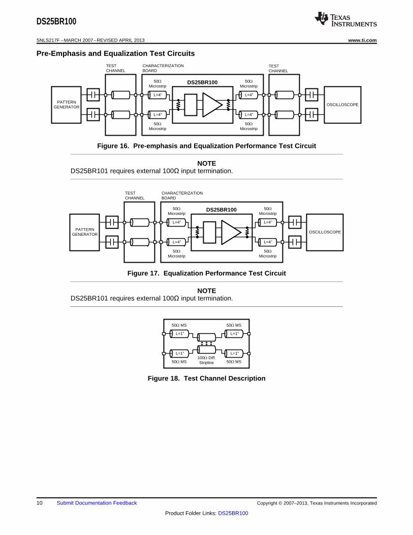
Pre-Emphasis and Equalization Test Circuits
Figure 16. Pre-emphasis and Equalization Performance Test Circuit
NOTEDS25BR101 requires external 100Ω input termination.
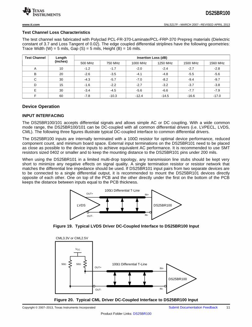
Figure 17. Equalization Performance Test Circuit
NOTEDS25BR101 requires external 100Ω input termination.
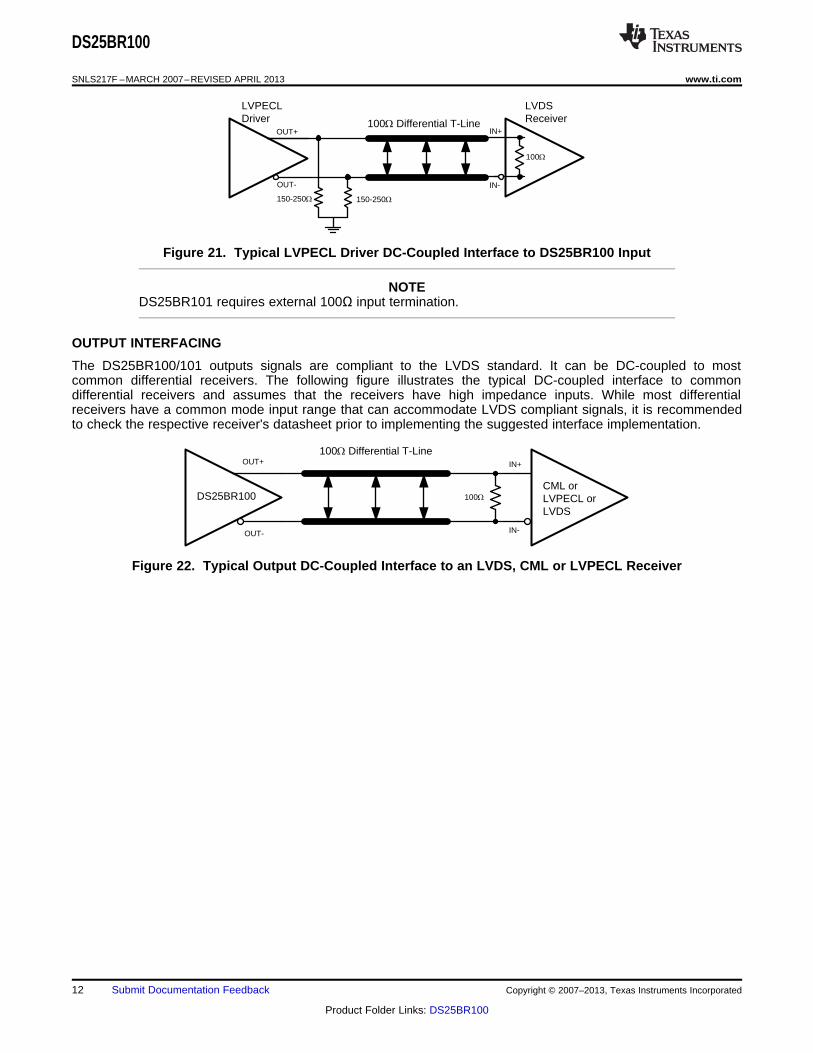
Figure 18. Test Channel Description
10 Submit Documentation Feedback Copyright © 2007–2013, Texas Instruments Incorporated
Product Folder Links: DS25BR100
OUT+
OUT-
DS25BR100
IN+
IN-
50:50:
VCC
CML3.3V or CML2.5V
100: Differential T-Line
OUT+
OUT-
DS25BR100
IN+
IN-
100: Differential T-Line
LVDS
DS25BR100
www.ti.com SNLS217F –MARCH 2007–REVISED APRIL 2013
Test Channel Loss Characteristics
The test channel was fabricated with Polyclad PCL-FR-370-Laminate/PCL-FRP-370 Prepreg materials (Dielectricconstant of 3.7 and Loss Tangent of 0.02). The edge coupled differential striplines have the following geometries:Trace Width (W) = 5 mils, Gap (S) = 5 mils, Height (B) = 16 mils.
Test Channel Length Insertion Loss (dB)(inches) 500 MHz 750 MHz 1000 MHz 1250 MHz 1500 MHz 1560 MHz
A 10 -1.2 -1.7 -2.0 -2.4 -2.7 -2.8
B 20 -2.6 -3.5 -4.1 -4.8 -5.5 -5.6
C 30 -4.3 -5.7 -7.0 -8.2 -9.4 -9.7
D 15 -1.6 -2.2 -2.7 -3.2 -3.7 -3.8
E 30 -3.4 -4.5 -5.6 -6.6 -7.7 -7.9
F 60 -7.8 -10.3 -12.4 -14.5 -16.6 -17.0
Device Operation
INPUT INTERFACING
The DS25BR100/101 accepts differential signals and allows simple AC or DC coupling. With a wide commonmode range, the DS25BR100/101 can be DC-coupled with all common differential drivers (i.e. LVPECL, LVDS,CML). The following three figures illustrate typical DC-coupled interface to common differential drivers.
The DS25BR100 inputs are internally terminated with a 100Ω resistor for optimal device performance, reducedcomponent count, and minimum board space. External input terminations on the DS25BR101 need to be placedas close as possible to the device inputs to achieve equivalent AC performance. It is recommended to use SMTresistors sized 0402 or smaller and to keep the mounting distance to the DS25BR101 pins under 200 mils.
When using the DS25BR101 in a limited multi-drop topology, any transmission line stubs should be kept veryshort to minimize any negative effects on signal quality. A single termination resistor or resistor network thatmatches the differential line impedance should be used. If DS25BR101 input pairs from two separate devices areto be connected to a single differential output, it is recommended to mount the DS25BR101 devices directlyopposite of each other. One on top of the PCB and the other directly under the first on the bottom of the PCBkeeps the distance between inputs equal to the PCB thickness.
Figure 19. Typical LVDS Driver DC-Coupled Interface to DS25BR100 Input
Figure 20. Typical CML Driver DC-Coupled Interface to DS25BR100 Input
Copyright © 2007–2013, Texas Instruments Incorporated Submit Documentation Feedback 11
Product Folder Links: DS25BR100
OUT+
OUT-
CML or LVPECL or LVDS
IN+
IN-
100:
100: Differential T-Line
DS25BR100
OUT+
OUT-
150-250:
100: Differential T-Line
LVDS Receiver
IN+
IN-
100:
LVPECL Driver
150-250:
DS25BR100
SNLS217F –MARCH 2007–REVISED APRIL 2013 www.ti.com
Figure 21. Typical LVPECL Driver DC-Coupled Interface to DS25BR100 Input
NOTEDS25BR101 requires external 100Ω input termination.
OUTPUT INTERFACING
The DS25BR100/101 outputs signals are compliant to the LVDS standard. It can be DC-coupled to mostcommon differential receivers. The following figure illustrates the typical DC-coupled interface to commondifferential receivers and assumes that the receivers have high impedance inputs. While most differentialreceivers have a common mode input range that can accommodate LVDS compliant signals, it is recommendedto check the respective receiver's datasheet prior to implementing the suggested interface implementation.
Figure 22. Typical Output DC-Coupled Interface to an LVDS, CML or LVPECL Receiver
12 Submit Documentation Feedback Copyright © 2007–2013, Texas Instruments Incorporated
Product Folder Links: DS25BR100
DS25BR100
www.ti.com SNLS217F –MARCH 2007–REVISED APRIL 2013
REVISION HISTORY
Changes from Revision E (April 2013) to Revision F Page
• Changed layout of National Data Sheet to TI format .......................................................................................................... 12
Copyright © 2007–2013, Texas Instruments Incorporated Submit Documentation Feedback 13
Product Folder Links: DS25BR100
PACKAGE OPTION ADDENDUM
www.ti.com 8-Oct-2015
Addendum-Page 1
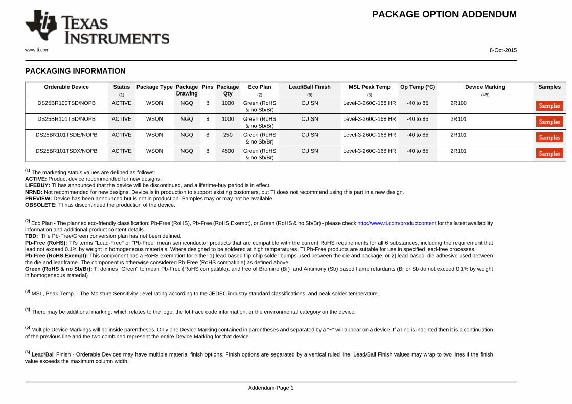
PACKAGING INFORMATION
Orderable Device Status(1)
Package Type PackageDrawing
Pins PackageQty
Eco Plan(2)
Lead/Ball Finish(6)
MSL Peak Temp(3)
Op Temp (°C) Device Marking(4/5)
Samples
DS25BR100TSD/NOPB ACTIVE WSON NGQ 8 1000 Green (RoHS& no Sb/Br)
CU SN Level-3-260C-168 HR -40 to 85 2R100
DS25BR101TSD/NOPB ACTIVE WSON NGQ 8 1000 Green (RoHS& no Sb/Br)
CU SN Level-3-260C-168 HR -40 to 85 2R101
DS25BR101TSDE/NOPB ACTIVE WSON NGQ 8 250 Green (RoHS& no Sb/Br)
CU SN Level-3-260C-168 HR -40 to 85 2R101
DS25BR101TSDX/NOPB ACTIVE WSON NGQ 8 4500 Green (RoHS& no Sb/Br)
CU SN Level-3-260C-168 HR -40 to 85 2R101
(1) The marketing status values are defined as follows:ACTIVE: Product device recommended for new designs.LIFEBUY: TI has announced that the device will be discontinued, and a lifetime-buy period is in effect.NRND: Not recommended for new designs. Device is in production to support existing customers, but TI does not recommend using this part in a new design.PREVIEW: Device has been announced but is not in production. Samples may or may not be available.OBSOLETE: TI has discontinued the production of the device.
(2) Eco Plan - The planned eco-friendly classification: Pb-Free (RoHS), Pb-Free (RoHS Exempt), or Green (RoHS & no Sb/Br) - please check http://www.ti.com/productcontent for the latest availabilityinformation and additional product content details.TBD: The Pb-Free/Green conversion plan has not been defined.Pb-Free (RoHS): TI's terms "Lead-Free" or "Pb-Free" mean semiconductor products that are compatible with the current RoHS requirements for all 6 substances, including the requirement thatlead not exceed 0.1% by weight in homogeneous materials. Where designed to be soldered at high temperatures, TI Pb-Free products are suitable for use in specified lead-free processes.Pb-Free (RoHS Exempt): This component has a RoHS exemption for either 1) lead-based flip-chip solder bumps used between the die and package, or 2) lead-based die adhesive used betweenthe die and leadframe. The component is otherwise considered Pb-Free (RoHS compatible) as defined above.Green (RoHS & no Sb/Br): TI defines "Green" to mean Pb-Free (RoHS compatible), and free of Bromine (Br) and Antimony (Sb) based flame retardants (Br or Sb do not exceed 0.1% by weightin homogeneous material)
(3) MSL, Peak Temp. - The Moisture Sensitivity Level rating according to the JEDEC industry standard classifications, and peak solder temperature.
(4) There may be additional marking, which relates to the logo, the lot trace code information, or the environmental category on the device.
(5) Multiple Device Markings will be inside parentheses. Only one Device Marking contained in parentheses and separated by a "~" will appear on a device. If a line is indented then it is a continuationof the previous line and the two combined represent the entire Device Marking for that device.
(6) Lead/Ball Finish - Orderable Devices may have multiple material finish options. Finish options are separated by a vertical ruled line. Lead/Ball Finish values may wrap to two lines if the finishvalue exceeds the maximum column width.
PACKAGE OPTION ADDENDUM
www.ti.com 8-Oct-2015
Addendum-Page 2
Important Information and Disclaimer:The information provided on this page represents TI's knowledge and belief as of the date that it is provided. TI bases its knowledge and belief on informationprovided by third parties, and makes no representation or warranty as to the accuracy of such information. Efforts are underway to better integrate information from third parties. TI has taken andcontinues to take reasonable steps to provide representative and accurate information but may not have conducted destructive testing or chemical analysis on incoming materials and chemicals.TI and TI suppliers consider certain information to be proprietary, and thus CAS numbers and other limited information may not be available for release.
In no event shall TI's liability arising out of such information exceed the total purchase price of the TI part(s) at issue in this document sold by TI to Customer on an annual basis.
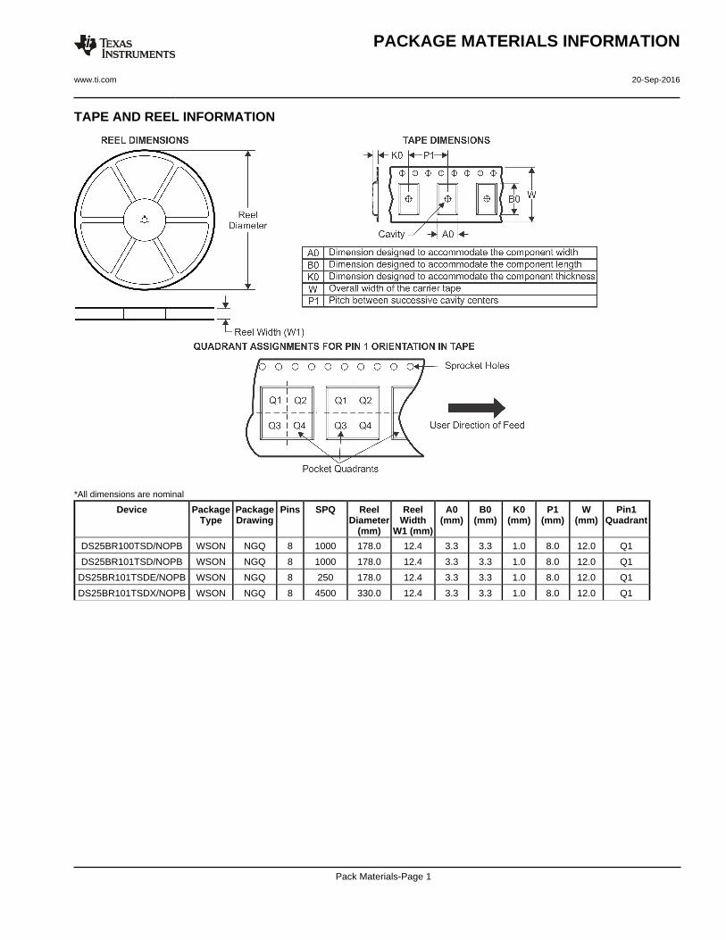
TAPE AND REEL INFORMATION
*All dimensions are nominal
Device PackageType
PackageDrawing
Pins SPQ ReelDiameter
(mm)
ReelWidth
W1 (mm)
A0(mm)
B0(mm)
K0(mm)
P1(mm)
W(mm)
Pin1Quadrant
DS25BR100TSD/NOPB WSON NGQ 8 1000 178.0 12.4 3.3 3.3 1.0 8.0 12.0 Q1
DS25BR101TSD/NOPB WSON NGQ 8 1000 178.0 12.4 3.3 3.3 1.0 8.0 12.0 Q1
DS25BR101TSDE/NOPB WSON NGQ 8 250 178.0 12.4 3.3 3.3 1.0 8.0 12.0 Q1
DS25BR101TSDX/NOPB WSON NGQ 8 4500 330.0 12.4 3.3 3.3 1.0 8.0 12.0 Q1
PACKAGE MATERIALS INFORMATION
www.ti.com 20-Sep-2016
Pack Materials-Page 1
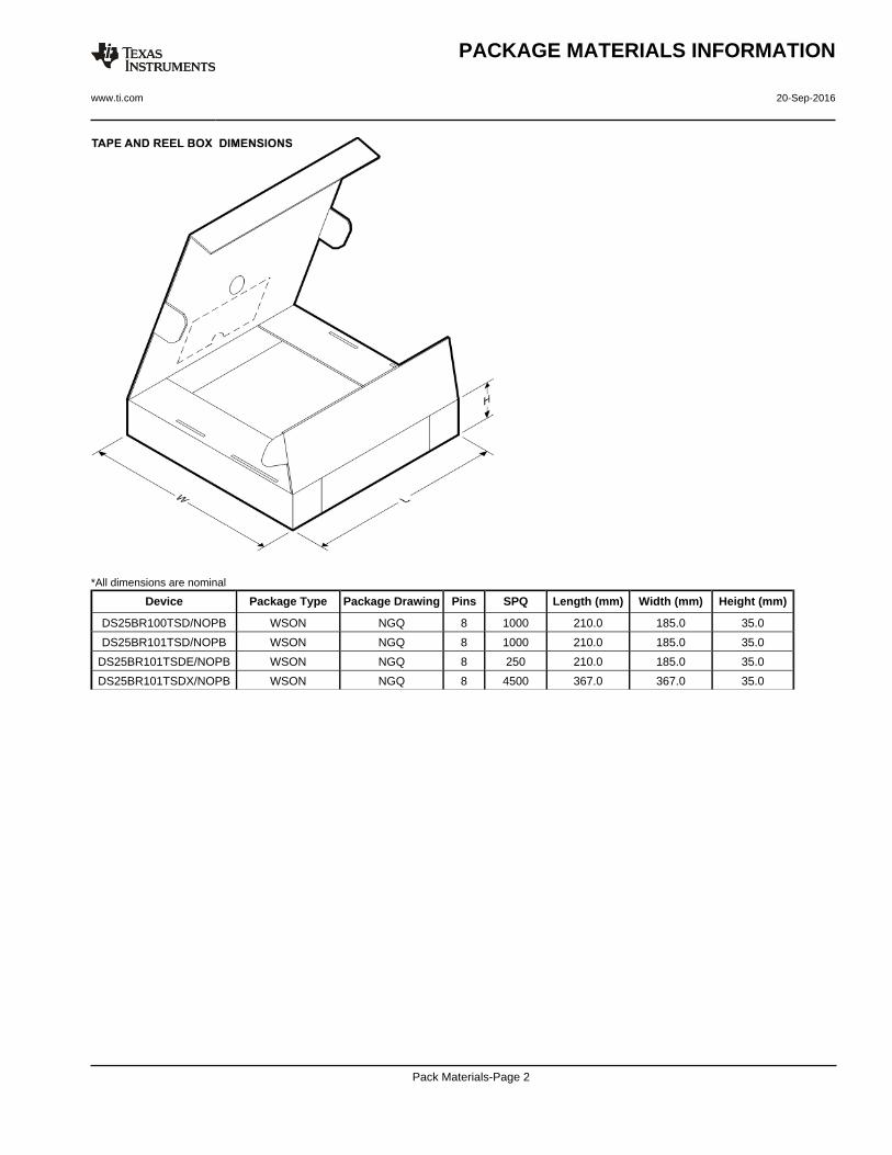
*All dimensions are nominal
Device Package Type Package Drawing Pins SPQ Length (mm) Width (mm) Height (mm)
DS25BR100TSD/NOPB WSON NGQ 8 1000 210.0 185.0 35.0
DS25BR101TSD/NOPB WSON NGQ 8 1000 210.0 185.0 35.0
DS25BR101TSDE/NOPB WSON NGQ 8 250 210.0 185.0 35.0
DS25BR101TSDX/NOPB WSON NGQ 8 4500 367.0 367.0 35.0
PACKAGE MATERIALS INFORMATION
www.ti.com 20-Sep-2016
Pack Materials-Page 2
www.ti.com
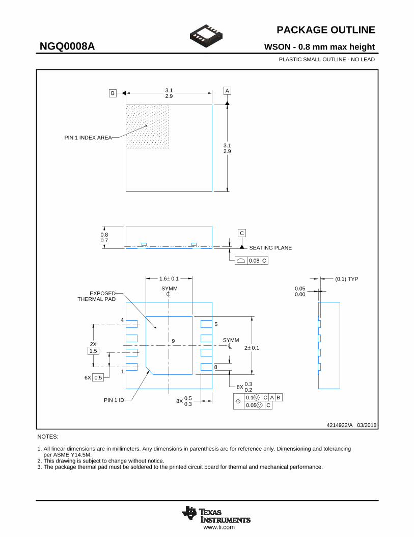
PACKAGE OUTLINE
C
8X 0.30.2
2 0.1
8X 0.50.3
2X1.5
1.6 0.1
6X 0.5
0.80.7
0.050.00
B 3.12.9
A
3.12.9
(0.1) TYP
WSON - 0.8 mm max heightNGQ0008APLASTIC SMALL OUTLINE - NO LEAD
4214922/A 03/2018
PIN 1 INDEX AREA
SEATING PLANE
0.08 C
1
45
8
PIN 1 ID 0.1 C A B0.05 C
THERMAL PADEXPOSED
9
SYMM
SYMM
NOTES: 1. All linear dimensions are in millimeters. Any dimensions in parenthesis are for reference only. Dimensioning and tolerancing per ASME Y14.5M. 2. This drawing is subject to change without notice. 3. The package thermal pad must be soldered to the printed circuit board for thermal and mechanical performance.
SCALE 4.000
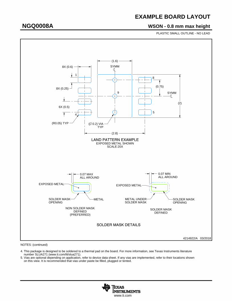
www.ti.com
EXAMPLE BOARD LAYOUT
0.07 MINALL AROUND
0.07 MAXALL AROUND
(1.6)
6X (0.5)
(2.8)
8X (0.25)
8X (0.6)
(2)
(R0.05) TYP ( 0.2) VIATYP
(0.75)
WSON - 0.8 mm max heightNGQ0008APLASTIC SMALL OUTLINE - NO LEAD
4214922/A 03/2018
SYMM
1
45
8
SYMM
LAND PATTERN EXAMPLEEXPOSED METAL SHOWN
SCALE:20X
9
NOTES: (continued) 4. This package is designed to be soldered to a thermal pad on the board. For more information, see Texas Instruments literature number SLUA271 (www.ti.com/lit/slua271).5. Vias are optional depending on application, refer to device data sheet. If any vias are implemented, refer to their locations shown on this view. It is recommended that vias under paste be filled, plugged or tented.
SOLDER MASKOPENINGSOLDER MASK
METAL UNDER
SOLDER MASKDEFINED
EXPOSED METAL
METALSOLDER MASKOPENING
SOLDER MASK DETAILS
NON SOLDER MASKDEFINED
(PREFERRED)
EXPOSED METAL
www.ti.com
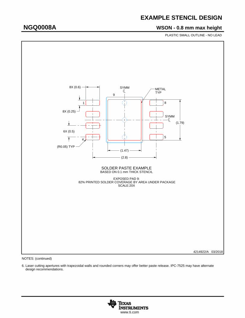
EXAMPLE STENCIL DESIGN
8X (0.25)
8X (0.6)
6X (0.5)
(1.79)
(1.47)
(2.8)
(R0.05) TYP
WSON - 0.8 mm max heightNGQ0008APLASTIC SMALL OUTLINE - NO LEAD
4214922/A 03/2018
NOTES: (continued) 6. Laser cutting apertures with trapezoidal walls and rounded corners may offer better paste release. IPC-7525 may have alternate design recommendations.
SOLDER PASTE EXAMPLEBASED ON 0.1 mm THICK STENCIL
EXPOSED PAD 9:
82% PRINTED SOLDER COVERAGE BY AREA UNDER PACKAGESCALE:20X
SYMM
1
45
8
SYMM
METALTYP
9
IMPORTANT NOTICE
Texas Instruments Incorporated (TI) reserves the right to make corrections, enhancements, improvements and other changes to itssemiconductor products and services per JESD46, latest issue, and to discontinue any product or service per JESD48, latest issue. Buyersshould obtain the latest relevant information before placing orders and should verify that such information is current and complete.TI’s published terms of sale for semiconductor products (http://www.ti.com/sc/docs/stdterms.htm) apply to the sale of packaged integratedcircuit products that TI has qualified and released to market. Additional terms may apply to the use or sale of other types of TI products andservices.Reproduction of significant portions of TI information in TI data sheets is permissible only if reproduction is without alteration and isaccompanied by all associated warranties, conditions, limitations, and notices. TI is not responsible or liable for such reproduceddocumentation. Information of third parties may be subject to additional restrictions. Resale of TI products or services with statementsdifferent from or beyond the parameters stated by TI for that product or service voids all express and any implied warranties for theassociated TI product or service and is an unfair and deceptive business practice. TI is not responsible or liable for any such statements.Buyers and others who are developing systems that incorporate TI products (collectively, “Designers”) understand and agree that Designersremain responsible for using their independent analysis, evaluation and judgment in designing their applications and that Designers havefull and exclusive responsibility to assure the safety of Designers' applications and compliance of their applications (and of all TI productsused in or for Designers’ applications) with all applicable regulations, laws and other applicable requirements. Designer represents that, withrespect to their applications, Designer has all the necessary expertise to create and implement safeguards that (1) anticipate dangerousconsequences of failures, (2) monitor failures and their consequences, and (3) lessen the likelihood of failures that might cause harm andtake appropriate actions. Designer agrees that prior to using or distributing any applications that include TI products, Designer willthoroughly test such applications and the functionality of such TI products as used in such applications.TI’s provision of technical, application or other design advice, quality characterization, reliability data or other services or information,including, but not limited to, reference designs and materials relating to evaluation modules, (collectively, “TI Resources”) are intended toassist designers who are developing applications that incorporate TI products; by downloading, accessing or using TI Resources in anyway, Designer (individually or, if Designer is acting on behalf of a company, Designer’s company) agrees to use any particular TI Resourcesolely for this purpose and subject to the terms of this Notice.TI’s provision of TI Resources does not expand or otherwise alter TI’s applicable published warranties or warranty disclaimers for TIproducts, and no additional obligations or liabilities arise from TI providing such TI Resources. TI reserves the right to make corrections,enhancements, improvements and other changes to its TI Resources. TI has not conducted any testing other than that specificallydescribed in the published documentation for a particular TI Resource.Designer is authorized to use, copy and modify any individual TI Resource only in connection with the development of applications thatinclude the TI product(s) identified in such TI Resource. NO OTHER LICENSE, EXPRESS OR IMPLIED, BY ESTOPPEL OR OTHERWISETO ANY OTHER TI INTELLECTUAL PROPERTY RIGHT, AND NO LICENSE TO ANY TECHNOLOGY OR INTELLECTUAL PROPERTYRIGHT OF TI OR ANY THIRD PARTY IS GRANTED HEREIN, including but not limited to any patent right, copyright, mask work right, orother intellectual property right relating to any combination, machine, or process in which TI products or services are used. Informationregarding or referencing third-party products or services does not constitute a license to use such products or services, or a warranty orendorsement thereof. Use of TI Resources may require a license from a third party under the patents or other intellectual property of thethird party, or a license from TI under the patents or other intellectual property of TI.TI RESOURCES ARE PROVIDED “AS IS” AND WITH ALL FAULTS. TI DISCLAIMS ALL OTHER WARRANTIES ORREPRESENTATIONS, EXPRESS OR IMPLIED, REGARDING RESOURCES OR USE THEREOF, INCLUDING BUT NOT LIMITED TOACCURACY OR COMPLETENESS, TITLE, ANY EPIDEMIC FAILURE WARRANTY AND ANY IMPLIED WARRANTIES OFMERCHANTABILITY, FITNESS FOR A PARTICULAR PURPOSE, AND NON-INFRINGEMENT OF ANY THIRD PARTY INTELLECTUALPROPERTY RIGHTS. TI SHALL NOT BE LIABLE FOR AND SHALL NOT DEFEND OR INDEMNIFY DESIGNER AGAINST ANY CLAIM,INCLUDING BUT NOT LIMITED TO ANY INFRINGEMENT CLAIM THAT RELATES TO OR IS BASED ON ANY COMBINATION OFPRODUCTS EVEN IF DESCRIBED IN TI RESOURCES OR OTHERWISE. IN NO EVENT SHALL TI BE LIABLE FOR ANY ACTUAL,DIRECT, SPECIAL, COLLATERAL, INDIRECT, PUNITIVE, INCIDENTAL, CONSEQUENTIAL OR EXEMPLARY DAMAGES INCONNECTION WITH OR ARISING OUT OF TI RESOURCES OR USE THEREOF, AND REGARDLESS OF WHETHER TI HAS BEENADVISED OF THE POSSIBILITY OF SUCH DAMAGES.Unless TI has explicitly designated an individual product as meeting the requirements of a particular industry standard (e.g., ISO/TS 16949and ISO 26262), TI is not responsible for any failure to meet such industry standard requirements.Where TI specifically promotes products as facilitating functional safety or as compliant with industry functional safety standards, suchproducts are intended to help enable customers to design and create their own applications that meet applicable functional safety standardsand requirements. Using products in an application does not by itself establish any safety features in the application. Designers mustensure compliance with safety-related requirements and standards applicable to their applications. Designer may not use any TI products inlife-critical medical equipment unless authorized officers of the parties have executed a special contract specifically governing such use.Life-critical medical equipment is medical equipment where failure of such equipment would cause serious bodily injury or death (e.g., lifesupport, pacemakers, defibrillators, heart pumps, neurostimulators, and implantables). Such equipment includes, without limitation, allmedical devices identified by the U.S. Food and Drug Administration as Class III devices and equivalent classifications outside the U.S.TI may expressly designate certain products as completing a particular qualification (e.g., Q100, Military Grade, or Enhanced Product).Designers agree that it has the necessary expertise to select the product with the appropriate qualification designation for their applicationsand that proper product selection is at Designers’ own risk. Designers are solely responsible for compliance with all legal and regulatoryrequirements in connection with such selection.Designer will fully indemnify TI and its representatives against any damages, costs, losses, and/or liabilities arising out of Designer’s non-compliance with the terms and provisions of this Notice.
Mailing Address: Texas Instruments, Post Office Box 655303, Dallas, Texas 75265Copyright © 2018, Texas Instruments Incorporated