Embed Size (px)
Citation preview

This is information on a product in full production.
December 2017 DocID6739 Rev 36 1/42
LD1086
1.5 A adjustable and fixed low drop positive voltage regulator
Datasheet - production data
Features
Typical dropout: 1.3 V at 1.5 A
Three-terminal adjustable or fixed output voltage: 1.8 V, 2.5 V, 3.3 V, 5 V, 12 V
Automotive grade (adjustable VOUT in TO-220 and DPAK packages only)
Output current guaranteed up to 1.5 A
Output tolerance: ± 1% at 25 °C and ± 2% in full temperature range
Internal power and thermal limit
Wide operating temperature range - 40 °C to 125 °C
Package available: TO-220, D²PAK, D²PAK/A, DPAK and DFN8 (4x4)
Pinout compatibility with standard adjustable voltage regulators
Description
The LD1086 is a low drop voltage regulator capable of providing up to 1.5 A of output current. Dropout is guaranteed at a maximum of 1.2 V at the maximum output current, decreasing at lower loads. The LD1086 is pin-to-pin compatible with older 3-terminal adjustable regulators, but has better performance in terms of drop and output tolerance. Unlike PNP regulators, where a part of the output current is wasted as quiescent current, the LD1086 quiescent current flows into the load, increasing efficiency. Only a 10 µF (minimum) capacitor is needed for stability. The device is available in a TO-220, D²PAK, D²PAK/A, DPAK or DFN8 (4x4) package. On-chip trimming allows the regulator to reach a very tight output voltage tolerance; within ± 1% at 25 °C. The LD1086 is available as automotive grade for adjustable output voltages in the TO-220 and DPAK packages. The PAT, SYL, SBL statistical tests have been performed, and the devices are qualified according to the AEC-Q100 specification for the automotive market in the temperature range of - 40 °C to 125 °C.
DPAK
D²PAK/A
TO-220
D²PAK DFN8 (4x4)
www.st.com

Contents LD1086
2/42 DocID6739 Rev 36
Contents
1 Diagram . . . . . . . . . . . . . . . . . . . . . . . . . . . . . . . . . . . . . . . . . . . . . . . . . . . 5
2 Pin configuration . . . . . . . . . . . . . . . . . . . . . . . . . . . . . . . . . . . . . . . . . . . . 6
3 Maximum ratings . . . . . . . . . . . . . . . . . . . . . . . . . . . . . . . . . . . . . . . . . . . . 7
4 Schematic application . . . . . . . . . . . . . . . . . . . . . . . . . . . . . . . . . . . . . . . 8
5 Electrical characteristics . . . . . . . . . . . . . . . . . . . . . . . . . . . . . . . . . . . . . 9
6 Typical application . . . . . . . . . . . . . . . . . . . . . . . . . . . . . . . . . . . . . . . . . 17
7 Package information . . . . . . . . . . . . . . . . . . . . . . . . . . . . . . . . . . . . . . . . 22
7.1 TO-220 (STD-ST dual gauge) type A package information . . . . . . . . . . . 23
7.2 DPAK package information . . . . . . . . . . . . . . . . . . . . . . . . . . . . . . . . . . . 25
7.3 D²PAK (SMD 2L STD-ST) type A package information . . . . . . . . . . . . . . 28
7.4 D²PAK (SMD 3L STD-ST) type A package information . . . . . . . . . . . . . . 30
7.5 DPAK and D²PAK packing information . . . . . . . . . . . . . . . . . . . . . . . . . . . 33
7.6 DFN8 (4x4) package information . . . . . . . . . . . . . . . . . . . . . . . . . . . . . . . 35
7.7 DFN8 (4x4) packing information . . . . . . . . . . . . . . . . . . . . . . . . . . . . . . . . 37
8 Ordering information . . . . . . . . . . . . . . . . . . . . . . . . . . . . . . . . . . . . . . . 39
9 Revision history . . . . . . . . . . . . . . . . . . . . . . . . . . . . . . . . . . . . . . . . . . . 40

DocID6739 Rev 36 3/42
LD1086 List of tables
42
List of tables
Table 1. Absolute maximum ratings . . . . . . . . . . . . . . . . . . . . . . . . . . . . . . . . . . . . . . . . . . . . . . . . . . 7Table 2. Thermal data. . . . . . . . . . . . . . . . . . . . . . . . . . . . . . . . . . . . . . . . . . . . . . . . . . . . . . . . . . . . . 7Table 3. Electrical characteristics of LD1086#18 . . . . . . . . . . . . . . . . . . . . . . . . . . . . . . . . . . . . . . . . 9Table 4. Electrical characteristics of LD1086#25 . . . . . . . . . . . . . . . . . . . . . . . . . . . . . . . . . . . . . . . 10Table 5. Electrical characteristics of LD1086#33 . . . . . . . . . . . . . . . . . . . . . . . . . . . . . . . . . . . . . . . 11Table 6. Electrical characteristics of LD1086#50 . . . . . . . . . . . . . . . . . . . . . . . . . . . . . . . . . . . . . . . 12Table 7. Electrical characteristics of LD1086#12 . . . . . . . . . . . . . . . . . . . . . . . . . . . . . . . . . . . . . . . 13Table 8. Electrical characteristics of LD1086B# . . . . . . . . . . . . . . . . . . . . . . . . . . . . . . . . . . . . . . . . 14Table 9. Electrical characteristics of LD1086# . . . . . . . . . . . . . . . . . . . . . . . . . . . . . . . . . . . . . . . . . 15Table 10. Electrical characteristics of LD1086DTTRY and LD1086VY (Automotive grade). . . . . . . . 16Table 11. TO-220 (STD-ST dual gauge) type A mechanical data . . . . . . . . . . . . . . . . . . . . . . . . . . . 24Table 12. DPAK mechanical data . . . . . . . . . . . . . . . . . . . . . . . . . . . . . . . . . . . . . . . . . . . . . . . . . . . . 26Table 13. D²PAK (SMD 2L STD-ST) type A mechanical data . . . . . . . . . . . . . . . . . . . . . . . . . . . . . . 29Table 14. D²PAK (SMD 3L STD-ST) type A mechanical data . . . . . . . . . . . . . . . . . . . . . . . . . . . . . . 31Table 15. DPAK and D²PAK tape and reel mechanical data . . . . . . . . . . . . . . . . . . . . . . . . . . . . . . . 34Table 16. DFN8 (4x4) mechanical data . . . . . . . . . . . . . . . . . . . . . . . . . . . . . . . . . . . . . . . . . . . . . . . 36Table 17. DFN8 (4x4) reel mechanical data . . . . . . . . . . . . . . . . . . . . . . . . . . . . . . . . . . . . . . . . . . . . 37Table 18. Order code . . . . . . . . . . . . . . . . . . . . . . . . . . . . . . . . . . . . . . . . . . . . . . . . . . . . . . . . . . . . . 39Table 19. Document revision history . . . . . . . . . . . . . . . . . . . . . . . . . . . . . . . . . . . . . . . . . . . . . . . . . 40

List of figures LD1086
4/42 DocID6739 Rev 36
List of figures
Figure 1. Schematic diagram . . . . . . . . . . . . . . . . . . . . . . . . . . . . . . . . . . . . . . . . . . . . . . . . . . . . . . . . 5Figure 2. Pin connections (top view) . . . . . . . . . . . . . . . . . . . . . . . . . . . . . . . . . . . . . . . . . . . . . . . . . . 6Figure 3. Application circuit . . . . . . . . . . . . . . . . . . . . . . . . . . . . . . . . . . . . . . . . . . . . . . . . . . . . . . . . . 8Figure 4. Output voltage vs. temp. (VI = 5 V). . . . . . . . . . . . . . . . . . . . . . . . . . . . . . . . . . . . . . . . . . . 17Figure 5. Output voltage vs. temp. (VI = 15 V). . . . . . . . . . . . . . . . . . . . . . . . . . . . . . . . . . . . . . . . . . 17Figure 6. Output voltage vs. temperature (VI = 4.25 V) . . . . . . . . . . . . . . . . . . . . . . . . . . . . . . . . . . . 17Figure 7. Short-circuit current vs. dropout voltage . . . . . . . . . . . . . . . . . . . . . . . . . . . . . . . . . . . . . . . 17Figure 8. Line regulation vs. temperature . . . . . . . . . . . . . . . . . . . . . . . . . . . . . . . . . . . . . . . . . . . . . 17Figure 9. Load regulation vs. temperature . . . . . . . . . . . . . . . . . . . . . . . . . . . . . . . . . . . . . . . . . . . . . 17Figure 10. Dropout voltage vs. temperature . . . . . . . . . . . . . . . . . . . . . . . . . . . . . . . . . . . . . . . . . . . . 18Figure 11. Dropout voltage vs. output current . . . . . . . . . . . . . . . . . . . . . . . . . . . . . . . . . . . . . . . . . . . 18Figure 12. Adjust pin current vs. input voltage. . . . . . . . . . . . . . . . . . . . . . . . . . . . . . . . . . . . . . . . . . . 18Figure 13. Adjust pin current vs. temperature . . . . . . . . . . . . . . . . . . . . . . . . . . . . . . . . . . . . . . . . . . . 18Figure 14. Adjust pin current vs. output current . . . . . . . . . . . . . . . . . . . . . . . . . . . . . . . . . . . . . . . . . . 18Figure 15. Quiescent current vs. output current. . . . . . . . . . . . . . . . . . . . . . . . . . . . . . . . . . . . . . . . . . 18Figure 16. Quiescent current vs. input voltage . . . . . . . . . . . . . . . . . . . . . . . . . . . . . . . . . . . . . . . . . . 19Figure 17. Supply voltage rejection vs. output current . . . . . . . . . . . . . . . . . . . . . . . . . . . . . . . . . . . . . 19Figure 18. Supply voltage rejection vs. frequency . . . . . . . . . . . . . . . . . . . . . . . . . . . . . . . . . . . . . . . . 19Figure 19. Supply voltage rejection vs. temperature . . . . . . . . . . . . . . . . . . . . . . . . . . . . . . . . . . . . . . 19Figure 20. Minimum load current vs. temperature . . . . . . . . . . . . . . . . . . . . . . . . . . . . . . . . . . . . . . . . 19Figure 21. Stability for adjustable. . . . . . . . . . . . . . . . . . . . . . . . . . . . . . . . . . . . . . . . . . . . . . . . . . . . . 19Figure 22. Stability for 2.85 V. . . . . . . . . . . . . . . . . . . . . . . . . . . . . . . . . . . . . . . . . . . . . . . . . . . . . . . . 20Figure 23. Stability for 12 V . . . . . . . . . . . . . . . . . . . . . . . . . . . . . . . . . . . . . . . . . . . . . . . . . . . . . . . . . 20Figure 24. Line transient (VI = 12 to 13 V) . . . . . . . . . . . . . . . . . . . . . . . . . . . . . . . . . . . . . . . . . . . . . . 20Figure 25. Line transient (IO = 200 mA). . . . . . . . . . . . . . . . . . . . . . . . . . . . . . . . . . . . . . . . . . . . . . . . 20Figure 26. Line transient (CADJ = 1 µF) . . . . . . . . . . . . . . . . . . . . . . . . . . . . . . . . . . . . . . . . . . . . . . . 20Figure 27. Load transient . . . . . . . . . . . . . . . . . . . . . . . . . . . . . . . . . . . . . . . . . . . . . . . . . . . . . . . . . . . 20Figure 28. Load transient (Trise = Tfall = 10 µs) . . . . . . . . . . . . . . . . . . . . . . . . . . . . . . . . . . . . . . . . . 21Figure 29. Thermal protection . . . . . . . . . . . . . . . . . . . . . . . . . . . . . . . . . . . . . . . . . . . . . . . . . . . . . . . 21Figure 30. TO-220 (STD-ST dual gauge) type A package outline . . . . . . . . . . . . . . . . . . . . . . . . . . . 23Figure 31. DPAK package outline. . . . . . . . . . . . . . . . . . . . . . . . . . . . . . . . . . . . . . . . . . . . . . . . . . . . 25Figure 32. DPAK recommended footprint (dimension are in mm) . . . . . . . . . . . . . . . . . . . . . . . . . . . 27Figure 33. D²PAK (SMD 2L STD-ST) type A package outline . . . . . . . . . . . . . . . . . . . . . . . . . . . . . . 28Figure 34. D²PAK (SMD 3L STD-ST) type A outline . . . . . . . . . . . . . . . . . . . . . . . . . . . . . . . . . . . . . . 30Figure 35. D²PAK (SMD 3L) recommended footprint . . . . . . . . . . . . . . . . . . . . . . . . . . . . . . . . . . . . . 32Figure 36. DPAK and D²PAK tape outline . . . . . . . . . . . . . . . . . . . . . . . . . . . . . . . . . . . . . . . . . . . . . . 33Figure 37. DPAK and D²PAK reel outline . . . . . . . . . . . . . . . . . . . . . . . . . . . . . . . . . . . . . . . . . . . . . . 34Figure 38. DFN8 (4x4) package outline . . . . . . . . . . . . . . . . . . . . . . . . . . . . . . . . . . . . . . . . . . . . . . . . 35Figure 39. DFN8 (4x4) recommended footprint . . . . . . . . . . . . . . . . . . . . . . . . . . . . . . . . . . . . . . . . . . 36Figure 40. DFN8 (4x4) tape outline (dimension are in mm). . . . . . . . . . . . . . . . . . . . . . . . . . . . . . . . . 37Figure 41. DFN8 (4x4) reel outline. . . . . . . . . . . . . . . . . . . . . . . . . . . . . . . . . . . . . . . . . . . . . . . . . . . . 38

DocID6739 Rev 36 5/42
LD1086 Diagram
42
1 Diagram
Figure 1. Schematic diagram

Pin configuration LD1086
6/42 DocID6739 Rev 36
2 Pin configuration
Note: The TAB is physically connected to the output (this is valid for the TO-220 package too).
Figure 2. Pin connections (top view)
D²PAK
D²PAK/A
TO-220
DFN8 (4x4)
OUTPUT
NC
NC
ADJ/GND
NC
IN
IN
NC
NC
AM11888v1
1
2
3
4 5
6
7
8
DPAK

DocID6739 Rev 36 7/42
LD1086 Maximum ratings
42
3 Maximum ratings
Note: Absolute maximum ratings are those values beyond which damage to the device may occur. Functional operation under these conditions is not implied.
Table 1. Absolute maximum ratings
Symbol Parameter Value Unit
VI DC input voltage 30 V
IO Output current Internally Limited mA
PD Power dissipation Internally Limited mW
TSTG Storage temperature range -55 to +150 °C
TJ Junction temperature range -40 to +150 °C
Table 2. Thermal data
Symbol Parameter TO-220D²PAK
D²PAK/ADPAK DFN8 (4x4) Unit
RthJC Thermal resistance junction-case 5 3 8 1.5 °C/W
RthJA Thermal resistance junction-ambient 50 62.5 100 33 °C/W

Schematic application LD1086
8/42 DocID6739 Rev 36
4 Schematic application
Figure 3. Application circuit
VO VREF 1R2
R1-------+
=

DocID6739 Rev 36 9/42
LD1086 Electrical characteristics
42
5 Electrical characteristics
VI = 4.8 V, CI = CO =10µF, TA = -40 to 125 °C, unless otherwise specified.
Table 3. Electrical characteristics of LD1086#18
Symbol Parameter Test conditions Min. Typ. Max. Unit
VO Output voltage (1)IO = 0 mA, TJ = 25 °C 1.782 1.8 1.818 V
IO = 0 to 1.5 A, VI = 3.4 to 30 V 1.764 1.8 1.836 V
VO Line regulation
IO = 0 mA, VI = 3.4 to 18 V, TJ = 25 °C
0.2 4 mV
IO = 0 mA, VI = 3.4 to 15 V 0.4 4 mV
VO Load regulationIO = 0 to 1.5 A, TJ = 25 °C 0.5 8 mV
IO = 0 to 1.5 A 1 16 mV
Vd Dropout voltage IO = 1.5 A 1.3 1.5 V
Iq Quiescent current VI 30 V 5 10 mA
Isc Short-circuit currentVI - VO = 5 V 1.5 2 A
VI - VO = 25 V 0.05 0.02 A
Thermal regulation TA = 25 °C, 30 ms pulse 0.01 0.04 %/W
SVR Supply voltage rejectionf = 120 Hz, CO = 25 µF, IO = 1.5 A
VI = 6.8 3 V60 82 dB
eNRMS output noise voltage
(% of VO)TA = 25 °C, f =10 Hz to 10 kHz 0.003 %
S Temperature stability 0.5 %
S Long term stability TA = 125 °C, 1000 Hrs 0.5 %
1. See short-circuit current curve for available output current at fixed dropout.

Electrical characteristics LD1086
10/42 DocID6739 Rev 36
VI = 5.5 V, CI = CO =10µF, TA = -40 to 125 °C, unless otherwise specified.
Table 4. Electrical characteristics of LD1086#25
Symbol Parameter Test conditions Min. Typ. Max. Unit
VO Output voltage (1)IO = 0 mA, TJ = 25 °C 2.475 2.5 2.525 V
IO = 0 to 1.5 A, VI = 4.1 to 30 V 2.45 2.5 2.55 V
VO Line regulation
IO = 0 mA, VI = 4.1 to 18 V,
TJ = 25 °C0.2 4 mV
IO = 0 mA, VI = 4.1 to 18 V 0.4 4 mV
VO Load regulationIO = 0 to 1.5 A, TJ = 25 °C 0.5 8 mV
IO = 0 to 1.5 A 1 16 mV
Vd Dropout voltage IO = 1.5 A 1.3 1.5 V
Iq Quiescent current VI 30 V 5 10 mA
Isc Short-circuit currentVI - VO = 5 V 1.5 2 A
VI - VO = 25 V 0.05 0.2 A
Thermal regulation TA = 25 °C, 30 ms pulse 0.008 0.04 %/W
SVR Supply voltage rejectionf = 120 Hz, CO = 25 µF, IO = 1.5 A
VI = 7.5 3 V60 81 dB
eNRMS output noise voltage (% of VO)
TA = 25 °C, f =10 Hz to 10 kHz 0.003 %
S Temperature stability 0.5 %
S Long term stability TA = 125 °C, 1000 Hrs 0.5 %
1. See short-circuit current curve for available output current at fixed dropout.

DocID6739 Rev 36 11/42
LD1086 Electrical characteristics
42
VI = 6.3 V, CI = CO =10µF, TA = -40 to 125 °C, unless otherwise specified.
Table 5. Electrical characteristics of LD1086#33
Symbol Parameter Test conditions Min. Typ. Max. Unit
VO Output voltage (1)IO = 0 mA, TJ = 25 °C 3.267 3.3 3.333 V
IO = 0 to 1.5 A, VI = 4.9 to 30 V 3.234 3.3 3.366 V
VO Line regulation
IO = 0 mA, VI = 4.9 to 18 V, TJ = 25 °C
0.5 6 mV
IO = 0 mA, VI = 4.9 to 18 V 1 6 mV
VO Load regulationIO = 0 to 1.5 A, TJ = 25 °C 1 10 mV
IO = 0 to 1.5 A 7 25 mV
Vd Dropout voltage IO = 1.5 A 1.3 1.5 V
Iq Quiescent current VI 30 V 5 10 mA
Isc Short-circuit currentVI - VO = 5 V 1.5 2 A
VI - VO = 25 V 0.05 0.2 A
Thermal regulation TA = 25 °C, 30 ms pulse 0.008 0.04 %/W
SVR Supply voltage rejectionf = 120 Hz, CO = 25 µF, IO = 1.5 AVI = 8.3 3 V
60 79 dB
eNRMS output noise voltage
(% of VO)TA = 25 °C, f =10 Hz to 10 kHz 0.003 %
S Temperature stability 0.5 %
S Long term stability TA = 125 °C, 1000 Hrs 0.5 %
1. See short-circuit current curve for available output current at fixed dropout.

Electrical characteristics LD1086
12/42 DocID6739 Rev 36
VI = 8 V, CI = CO =10µF, TA = -40 to 125 °C, unless otherwise specified.
Table 6. Electrical characteristics of LD1086#50
Symbol Parameter Test conditions Min. Typ. Max. Unit
VO Output voltage (1)IO = 0 mA, TJ = 25 °C 4.95 5 5.05 V
IO = 0 to 1.5 A, VI = 6.6 to 30 V 4.9 5 5.1 V
VO Line regulation
IO = 0 mA, VI = 6.6 to 20V, TJ = 25 °C
0.5 10 mV
IO = 0 mA, VI = 6.6 to 20 V 1 10 mV
VO Load regulationIO = 0 to 1.5 A, TJ = 25 °C 5 20 mV
IO = 0 to 1.5 A 10 35 mV
Vd Dropout voltage IO = 1.5 A 1.3 1.5 V
Iq Quiescent current VI 30 V 5 10 mA
Isc Short-circuit currentVI - VO = 5 V 1.5 2 A
VI - VO = 25 V 0.05 0.2 A
Thermal regulation TA = 25 °C, 30 ms pulse 0.01 0.04 %/W
SVR Supply voltage rejectionf = 120 Hz, CO = 25 µF, IO = 1.5 AVI = 10 3 V
60 75 dB
eNRMS output noise voltage (% of VO)
TA = 25 °C, f =10 Hz to 10 kHz 0.003 %
S Temperature stability 0.5 %
S Long term stability TA = 125 °C, 1000 Hrs 0.5 %
1. See short-circuit current curve for available output current at fixed dropout.

DocID6739 Rev 36 13/42
LD1086 Electrical characteristics
42
VI = 15 V, CI = CO =10µF, TA = -40 to 125 °C, unless otherwise specified.
Table 7. Electrical characteristics of LD1086#12
Symbol Parameter Test conditions Min. Typ. Max. Unit
VO Output voltage (1)IO = 0 mA, TJ = 25 °C 11.88 12 12.12 V
IO = 0 to 1.5 A, VI = 13.8 to 30 V 11.76 12 12.24 V
VO Line regulation
IO = 0 mA, VI = 13.8 to 25 V,TJ = 25 °C
1 25 mV
IO = 0 mA, VI = 13.8 to 25 V 2 25 mV
VO Load regulationIO = 0 to 1.5 A, TJ = 25 °C 12 36 mV
IO = 0 to 1.5 A 24 72 mV
Vd Dropout voltage IO = 1.5 A 1.3 1.5 V
Iq Quiescent current VI 30 V 5 10 mA
Isc Short-circuit currentVI - VO = 5 V 1.5 2 A
VI - VO = 25 V 0.05 0.2 A
Thermal regulation TA = 25 °C, 30 ms pulse 0.01 0.04 %/W
SVR Supply voltage rejectionf = 120 Hz, CO = 25 µF, IO = 1.5 A VI = 17 3 V
54 66 dB
eNRMS output noise voltage
(% of VO)TA = 25 °C, f =10 Hz to 10 kHz 0.003 %
S Temperature stability 0.5 %
S Long term stability TA = 125 °C, 1000 Hrs 0.5 %
1. See short-circuit current curve for available output current at fixed dropout.

Electrical characteristics LD1086
14/42 DocID6739 Rev 36
VI = 4.25 V, CI = CO =10µF, TA = -40 to 125 °C, unless otherwise specified.
Table 8. Electrical characteristics of LD1086B#
Symbol Parameter Test conditions Min. Typ. Max. Unit
Vref Reference voltage (1)
IO = 10 mA TJ = 25 °C 1.231 1.25 1.269 V
IO = 10 mA to 1.5 A, VI = 2.85 to 30 V
1.219 1.25 1.281 V
VO Line regulation
IO = 10 mA, VI = 2.8 to 16.5 V,TJ = 25 °C
0.015 0.2 %
IO = 10 mA, VI = 2.8 to 16.5 V 0.035 0.2 %
VO Load regulationIO = 10 mA to 1.5 A, TJ = 25 °C 0.1 0.3 %
IO = 0 to 1.5 A 0.2 0.4 %
Vd Dropout voltage IO = 1.5 A 1.3 1.5 V
IO(min) Minimum load current VI 30 V 3 10 mA
Isc Short-circuit currentVI - VO = 5 V 1.5 2.3 A
VI - VO = 25 V 0.05 0.2 A
Thermal regulation TA = 25 °C, 30 ms pulse 0.01 0.04 %/W
SVR Supply voltage rejectionf = 120 Hz, CO = 25 µF,CADJ = 25 µF,IO = 1.5 A, VI = 6.25 3 V
60 88 dB
IADJ Adjust pin current VI 4.25 V, IO = 10 mA 40 120 µA
IADJ Adjust pin current change (1) IO = 10 mA to 1.5 A, VI = 2.8 to 16.5 V
0.2 5 µA
eNRMS output noise voltage
(% of VO)TA = 25 °C, f =10 Hz to 10 kHz 0.003 %
S Temperature stability 0.5 %
S Long term stability TA = 125 °C, 1000 Hrs 0.5 %
1. See short-circuit current curve for available output current at fixed dropout.

DocID6739 Rev 36 15/42
LD1086 Electrical characteristics
42
VI = 4.25 V, CI = CO =10µF, TA = -40 to 125 °C, unless otherwise specified.
Table 9. Electrical characteristics of LD1086#
Symbol Parameter Test conditions Min. Typ. Max. Unit
Vref Reference voltage (1)
IO = 10 mA TJ = 25 °C 1.237 1.25 1.263 V
IO = 10 mA to 1.5 A, VI = 2.85 to 30 V
1.225 1.25 1.275 V
VO Line regulation
IO = 10 mA, VI = 2.8 to 16.5 V,TJ = 25 °C
0.015 0.2 %
IO = 10 mA, VI = 2.8 to 16.5 V 0.035 0.2 %
VO Load regulationIO = 10 mA to 1.5 A, TJ = 25 °C 0.1 0.3 %
IO = 0 to 1.5 A 0.2 0.4 %
Vd Dropout voltage IO = 1.5 A 1.3 1.5 V
IO(min) Minimum load current VI 30 V 3 10 mA
Isc Short-circuit currentVI - VO = 5 V 1.5 2.3 A
VI - VO = 25 V 0.05 0.2 A
Thermal regulation TA = 25 °C, 30 ms pulse 0.01 0.04 %/W
SVR Supply voltage rejectionf = 120 Hz, CO = 25 µF,CADJ = 25 µF,IO = 1.5 A, VI = 6.25 3 V
60 88 dB
IADJ Adjust pin current VI 4.25 V, IO = 10 mA 40 120 µA
IADJ Adjust pin current change (1) IO = 10 mA to 1.5 A, VI = 2.8 to 16.5 V
0.2 5 µA
eNRMS output noise voltage
(% of VO)TA = 25 °C, f =10 Hz to 10 kHz 0.003 %
S Temperature stability 0.5 %
S Long term stability TA = 125 °C, 1000 Hrs 0.5 %
1. See short-circuit current curve for available output current at fixed dropout.

Electrical characteristics LD1086
16/42 DocID6739 Rev 36
VI = 4.25 V, CI = CO =10µF, TA = -40 to 125 °C, unless otherwise specified.
Table 10. Electrical characteristics of LD1086DTTRY and LD1086VY (Automotive grade)
Symbol Parameter Test conditions Min. Typ. Max. Unit
Vref Reference voltage (1)IO = 10 mA TA = 25 °C 1.237 1.25 1.263 V
IO = 10 mA to 1.5 A, VI = 2.85 to 30 V 1.225 1.25 1.275 V
VO Line regulation IO = 10 mA, VI = 2.8 to 16.5 V 0.035 0.2 %
VO Load regulation IO = 0 to 1.5 A 0.2 0.4 %
Vd Dropout voltage IO = 1.5 A 1.3 1.5 V
IO(min) Minimum load current VI 30 V 3 10 mA
Isc Short-circuit currentVI - VO = 5 V, TA = 25 °C 1.5 2.3 A
VI - VO = 25 V, TA = 25 °C 0.05 0.2 A
Thermal regulation TA = 25 °C, 30 ms pulse 0.01 0.04 %/W
SVR Supply voltage rejectionf = 120 Hz, CO = 25 µF,CADJ = 25 µF,IO = 1.5 A, VI = 6.25 3 V, TA = 25 °C
60 88 dB
IADJ Adjust pin current VI 4.25 V, IO = 10 mA 40 120 A
IADJ Adjust pin current change (1) IO = 10 mA to 1.5 A, VI = 2.8 to 16.5 V 0.2 5 A
eNRMS output noise voltage
(% of VO)TA = 25 °C, f =10 Hz to 10 kHz 0.003 %
S Temperature stability 0.5 %
S Long term stability TA = 125 °C, 1000 Hrs 0.5 %
1. See short-circuit current curve for available output current at fixed dropout.

DocID6739 Rev 36 17/42
LD1086 Typical application
42
6 Typical application
Unless otherwise specified TJ = 25 °C, CI = CO = 10 µF.
Figure 4. Output voltage vs. temp. (VI = 5 V) Figure 5. Output voltage vs. temp. (VI = 15 V)
Figure 6. Output voltage vs. temperature (VI = 4.25 V)
Figure 7. Short-circuit current vs. dropout voltage
Figure 8. Line regulation vs. temperature Figure 9. Load regulation vs. temperature

Typical application LD1086
18/42 DocID6739 Rev 36
Figure 10. Dropout voltage vs. temperature Figure 11. Dropout voltage vs. output current
Figure 12. Adjust pin current vs. input voltage Figure 13. Adjust pin current vs. temperature
Figure 14. Adjust pin current vs. output current Figure 15. Quiescent current vs. output current
DocID6739 Rev 36 19/42
LD1086 Typical application
42
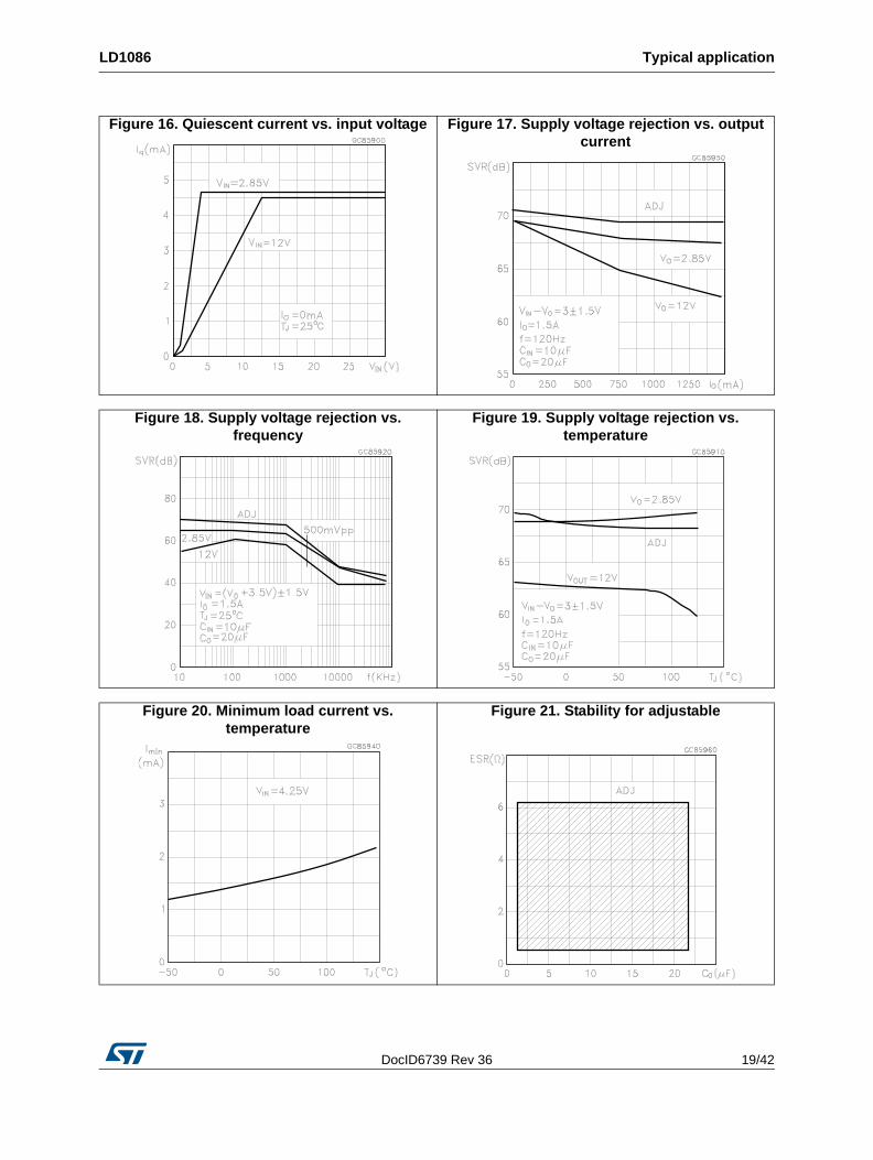
Figure 16. Quiescent current vs. input voltage Figure 17. Supply voltage rejection vs. output current
Figure 18. Supply voltage rejection vs. frequency
Figure 19. Supply voltage rejection vs. temperature
Figure 20. Minimum load current vs. temperature
Figure 21. Stability for adjustable

Typical application LD1086
20/42 DocID6739 Rev 36
Figure 22. Stability for 2.85 V Figure 23. Stability for 12 V
Figure 24. Line transient (VI = 12 to 13 V)
VI = 12 to 13 V, IO = 200 mA, CI = 1 µF (tant), CO = 10 µF (tant), No CADJ
Figure 25. Line transient (IO = 200 mA)
VI = 12 to 13 V, IO = 200 mA, CI = 1 µF (tant), CO = 10 µF (tant), No CADJ
Figure 26. Line transient (CADJ = 1 µF)
VI = 12 to 13 V, IO = 200 mA, CI = 1 µF (tant), CO = 10 µF (tant), CADJ = 1 µF
Figure 27. Load transient
VI = 13 V, IO = 0.1 to 1.5 A, CI = 1 µF (tant), CO = 10 µF (tant) CADJ = 1 µF

DocID6739 Rev 36 21/42
LD1086 Typical application
42
Figure 28. Load transient (Trise = Tfall = 10 µs)
VI = 13 V, IO = 0.1 to 1.5 A, CI = 1 µF (tant), CO = 10 µF (tant), CADJ = 1 µF
Figure 29. Thermal protection
VO = 2.85 V

Package information LD1086
22/42 DocID6739 Rev 36
7 Package information
In order to meet environmental requirements, ST offers these devices in different grades of ECOPACK® packages, depending on their level of environmental compliance. ECOPACK® specifications, grade definitions and product status are available at: www.st.com. ECOPACK® is an ST trademark.

DocID6739 Rev 36 23/42
LD1086 Package information
42
7.1 TO-220 (STD-ST dual gauge) type A package information
Figure 30. TO-220 (STD-ST dual gauge) type A package outline

Package information LD1086
24/42 DocID6739 Rev 36
Table 11. TO-220 (STD-ST dual gauge) type A mechanical data
Dim.mm
Min. Typ. Max.
A 4.40 4.60
b 0.61 0.88
b1 1.14 1.70
c 0.48 0.70
D 15.25 15.75
D1 1.27
E 10 10.40
e 2.40 2.70
e1 4.95 5.15
F 1.23 1.32
H1 6.20 6.60
J1 2.40 2.72
L 13 14
L1 3.50 3.93
L20 16.40
L30 28.90
P 3.75 3.85
Q 2.65 2.95

DocID6739 Rev 36 25/42
LD1086 Package information
42
7.2 DPAK package information
Figure 31. DPAK package outline
0068772_K

Package information LD1086
26/42 DocID6739 Rev 36
Table 12. DPAK mechanical data
Dim.mm
Min. Typ. Max.
A 2.20 2.40
A1 0.90 1.10
A2 0.03 0.23
b 0.64 0.90
b4 5.20 5.40
c 0.45 0.60
c2 0.48 0.60
D 6.00 6.20
D1 5.10
E 6.40 6.60
E1 4.70
e 2.28
e1 4.40 4.60
H 9.35 10.10
L 1.00 1.50
(L1) 2.80
L2 0.80
L4 0.60 1.00
R 0.20
V2 0° 8°

DocID6739 Rev 36 27/42
LD1086 Package information
42
Figure 32. DPAK recommended footprint (dimension are in mm)
Footprint_REV_K

Package information LD1086
28/42 DocID6739 Rev 36
7.3 D²PAK (SMD 2L STD-ST) type A package information
Figure 33. D²PAK (SMD 2L STD-ST) type A package outline
0079457_T

DocID6739 Rev 36 29/42
LD1086 Package information
42
Table 13. D²PAK (SMD 2L STD-ST) type A mechanical data
Dim.mm
Min. Typ. Max.
A 4.40 4.60
A1 0.03 0.23
b 0.70 0.93
b2 1.14 1.70
c 0.45 0.60
c2 1.23 1.36
D 8.95 9.35
D1 7.50
E 10 10.40
E1 8.50
e 2.54
e1 4.88 5.28
H 15 15.85
J1 2.49 2.69
L 2.29 2.79
L1 1.27 1.40
L2 1.30 1.75
R 0.4
V2 0° 8°

Package information LD1086
30/42 DocID6739 Rev 36
7.4 D²PAK (SMD 3L STD-ST) type A package information
Figure 34. D²PAK (SMD 3L STD-ST) type A outline
7106164_E

DocID6739 Rev 36 31/42
LD1086 Package information
42
Table 14. D²PAK (SMD 3L STD-ST) type A mechanical data
Dim.mm
Min. Typ. Max.
A 4.40 4.60
A1 0.03 0.23
b 0.70 0.93
b1 0.80 1.30
b2 1.14 1.70
c 0.45 0.60
c2 1.23 1.36
D 8.95 9.35
D1 7.50
E 10 10.40
E1 8.50
e 2.54
e1 4.88 5.28
H 15 15.85
J1 2.49 2.69
L 2.29 2.79
L1 1.27 1.40
R 0.4
V2 0° 8°

Package information LD1086
32/42 DocID6739 Rev 36
Figure 35. D²PAK (SMD 3L) recommended footprint

DocID6739 Rev 36 33/42
LD1086 Package information
42
7.5 DPAK and D²PAK packing information
Figure 36. DPAK and D²PAK tape outline
P1A0 D1
P0
F
W
E
D
B0K0
T
User direction of feed
P2
10 pitches cumulativetolerance on tape +/- 0.2 mm
User direction of feed
R
Bending radius
B1
For machine ref. onlyincluding draft andradii concentric around B0
AM08852v1
Top covertape

Package information LD1086
34/42 DocID6739 Rev 36
Figure 37. DPAK and D²PAK reel outline
Table 15. DPAK and D²PAK tape and reel mechanical data
Tape Reel
Dim.mm
Dim.mm
Min. Max. Min. Max.
A0 6.8 7 A 330
B0 10.4 10.6 B 1.5
B1 12.1 C 12.8 13.2
D 1.5 1.6 D 20.2
D1 1.5 G 16.4 18.4
E 1.65 1.85 N 50
F 7.4 7.6 T 22.4
K0 2.55 2.75
P0 3.9 4.1 Base qty. 2500
P1 7.9 8.1 Bulk qty. 2500
P2 1.9 2.1
R 40
T 0.25 0.35
W 15.7 16.3
A
D
B
Full radius G measured at hub
C
N
REEL DIMENSIONS
40mm min.
Access hole
At sl ot location
T
Tape slot in core fortape start 25 mm min.width
AM08851v2

DocID6739 Rev 36 35/42
LD1086 Package information
42
7.6 DFN8 (4x4) package information
Figure 38. DFN8 (4x4) package outline

Package information LD1086
36/42 DocID6739 Rev 36
Figure 39. DFN8 (4x4) recommended footprint
Table 16. DFN8 (4x4) mechanical data
Dim.mm.
Min. Typ. Max.
A 0.80 0.90 1
A1 0 0.02 0.05
A3 0,20
b 0.23 0.30 0.38
D 3.90 4 4.10
D2 2.82 3 3.23
E 3.90 4 4.10
E2 2.05 2.20 2.30
e 0.80
L 0.40 0.50 0.60

DocID6739 Rev 36 37/42
LD1086 Package information
42
7.7 DFN8 (4x4) packing information
Figure 40. DFN8 (4x4) tape outline (dimension are in mm)
Table 17. DFN8 (4x4) reel mechanical data
Dim.mm. inch.
Min. Typ. Max. Min. Typ. Max.
A 330 12.992
C 12.8 13.0 13.2 0.504 0.512 0.519
D 20.2 0.795
N 60 2.362
T 22.4 0.882
7279936

Package information LD1086
38/42 DocID6739 Rev 36
Figure 41. DFN8 (4x4) reel outline
DocID6739 Rev 36 39/42
LD1086 Ordering information
42
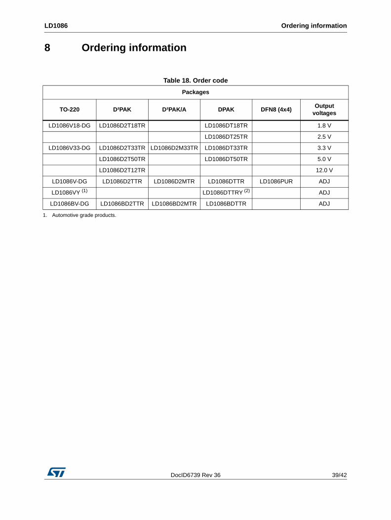
8 Ordering information
Table 18. Order code
Packages
TO-220 D²PAK D²PAK/A DPAK DFN8 (4x4)Output
voltages
LD1086V18-DG LD1086D2T18TR LD1086DT18TR 1.8 V
LD1086DT25TR 2.5 V
LD1086V33-DG LD1086D2T33TR LD1086D2M33TR LD1086DT33TR 3.3 V
LD1086D2T50TR LD1086DT50TR 5.0 V
LD1086D2T12TR 12.0 V
LD1086V-DG LD1086D2TTR LD1086D2MTR LD1086DTTR LD1086PUR ADJ
LD1086VY (1) LD1086DTTRY (2) ADJ
LD1086BV-DG LD1086BD2TTR LD1086BD2MTR LD1086BDTTR ADJ
1. Automotive grade products.

Revision history LD1086
40/42 DocID6739 Rev 36
9 Revision history
Table 19. Document revision history
Date Revision Changes
16-May-2006 14 Order codes updated and new template.
19-Jan-2007 15 D²PAK mechanical data updated and add footprint data.
05-Apr-2007 16 Order codes updated.
07-Jun-2007 17 Order codes updated.
19-Jul-2007 18 Add note on Figure 2.
03-Dec-2007 19 Modified: Table 18.
31-Jan-2008 20 Added new order codes for Automotive grade products.
18-Feb-2008 21 Modified: Table 18 on page 39.
14-Jul-2008 22 Modified: Table 1 on page 7 and Table 18 on page 39.
10-Mar-2010 23Added: Table 12 on page 26, Figure 30 on page 23, Figure 31 on page 25, Figure 31 and Figure 32 on page 27.
15-Nov-2010 24 Modified: RthJC value for TO-220 Table 2 on page 7.
11-Jul-2011 25 Modified: Figure 24, Figure 25 on page 20 and Table 18 on page 39.
10-Feb-2012 26 Added: order code LD1086V-DG Table 18 on page 39.
15-Mar-2012 27Added: new order code LD1086PUR Table 18 on page 39 and new package mechanical data DFN8 (4x4 mm) Table 16 on page 36, Figure 38 on page 35, Figure 39 on page 36, Figure 40 on page 37 and Figure 41 on page 38.
19-Oct-2012 28 Added: RthJA value for DPAK Table 2 on page 7.
13-Feb-2013 29Modified: Output voltage in Voltage reference parameter Table 8 on page 14 and Table 10 on page 16.
01-Mar-2013 30 Modified: DFN8 (4 x 4) pin configuration Figure 2 on page 6.
17-Jun-2013 31
Added Table 8: Electrical characteristics of LD1086B# and Section 7.7: DFN8 (4x4) packing information.
Updated Section 7: Package information and Table 18: Order code.
Minor text changes.
22-Oct-2013 32
RPN LD1086xx changed to LD1086.Updated the Description in cover page.Cancelled Table 1: Device summary.Updated Figure 2: Pin connections (top view), Section 5: Electrical characteristics, Section 7: Package information and Table 18: Order code.Minor text changes.
18-Dec-2014 33Updated Table 6.: Electrical characteristics of LD1086#50, Section 7: Package information and Section 7.7: DFN8 (4x4) packing information.Minor text changes.
10-Feb-2015 34 Updated Table 18: Order code.Minor text changes.

DocID6739 Rev 36 41/42
LD1086 Revision history
42
16-Nov-2015 35 Updated Section 7: Package information and Table 18: Order codeMinor text changes.
19-Dec-2017 36 Updated TJ value in Table 1: Absolute maximum ratings.
Table 19. Document revision history (continued)
Date Revision Changes

LD1086
42/42 DocID6739 Rev 36
IMPORTANT NOTICE – PLEASE READ CAREFULLY
STMicroelectronics NV and its subsidiaries (“ST”) reserve the right to make changes, corrections, enhancements, modifications, and improvements to ST products and/or to this document at any time without notice. Purchasers should obtain the latest relevant information on ST products before placing orders. ST products are sold pursuant to ST’s terms and conditions of sale in place at the time of order acknowledgement.
Purchasers are solely responsible for the choice, selection, and use of ST products and ST assumes no liability for application assistance or the design of Purchasers’ products.
No license, express or implied, to any intellectual property right is granted by ST herein.
Resale of ST products with provisions different from the information set forth herein shall void any warranty granted by ST for such product.
ST and the ST logo are trademarks of ST. All other product or service names are the property of their respective owners.
Information in this document supersedes and replaces information previously supplied in any prior versions of this document.
© 2017 STMicroelectronics – All rights reserved