Embed Size (px)
Citation preview
This is information on a product in full production.
April 2015 DocID2141 Rev 14 1/25
L4940
1.5 A very low drop voltage regulator IC
Datasheet - production data
Features• Precise 5, 8.5, 12 V outputs
• Low dropout voltage (450 mV typ. at 1 A)
• Very low quiescent current
• Thermal shutdown
• Short-circuit protection
• Reverse polarity protection
DescriptionThe L4940 series of three-terminal positive regulators is available in TO-220 and D²PAK packages and with several fixed output voltages, making it useful in a wide range of industrial and consumer applications. Thanks to their very low input/output voltage drop, these devices are particularly suitable for battery-powered equipment, reducing consumption and prolonging battery-life. Each type employs internal current limiting, anti-saturation circuit, thermal shutdown and safe area protection.
TO-220
D²PAK
Table 1. Device summary
Order code Output voltagesTO-220 D²PAK
L4940V5 L4940D2T5-TR 5 V
L4940V85 8.5 V
L4940D2T12-TR 12 V
www.st.com
Contents L4940
2/25 DocID2141 Rev 14
Contents
1 Block diagram . . . . . . . . . . . . . . . . . . . . . . . . . . . . . . . . . . . . . . . . . . . . . . 3
2 Pin configuration . . . . . . . . . . . . . . . . . . . . . . . . . . . . . . . . . . . . . . . . . . . 4
3 Maximum ratings . . . . . . . . . . . . . . . . . . . . . . . . . . . . . . . . . . . . . . . . . . . . 5
4 Test circuits . . . . . . . . . . . . . . . . . . . . . . . . . . . . . . . . . . . . . . . . . . . . . . . 6
5 Electrical characteristics . . . . . . . . . . . . . . . . . . . . . . . . . . . . . . . . . . . . . 7
6 Performance characteristics . . . . . . . . . . . . . . . . . . . . . . . . . . . . . . . . . . 9
7 Application circuits . . . . . . . . . . . . . . . . . . . . . . . . . . . . . . . . . . . . . . . . . 13
8 Package information . . . . . . . . . . . . . . . . . . . . . . . . . . . . . . . . . . . . . . . . 15
8.1 TO-220 (dual gauge) package information . . . . . . . . . . . . . . . . . . . . . . . . 16
8.2 TO-220 (dual gauge) packing information . . . . . . . . . . . . . . . . . . . . . . . . 18
8.3 D²PAK package information . . . . . . . . . . . . . . . . . . . . . . . . . . . . . . . . . . . 19
8.4 D²PAK packing information . . . . . . . . . . . . . . . . . . . . . . . . . . . . . . . . . . . 22
9 Revision history . . . . . . . . . . . . . . . . . . . . . . . . . . . . . . . . . . . . . . . . . . . 24
DocID2141 Rev 14 3/25
L4940 Block diagram
25
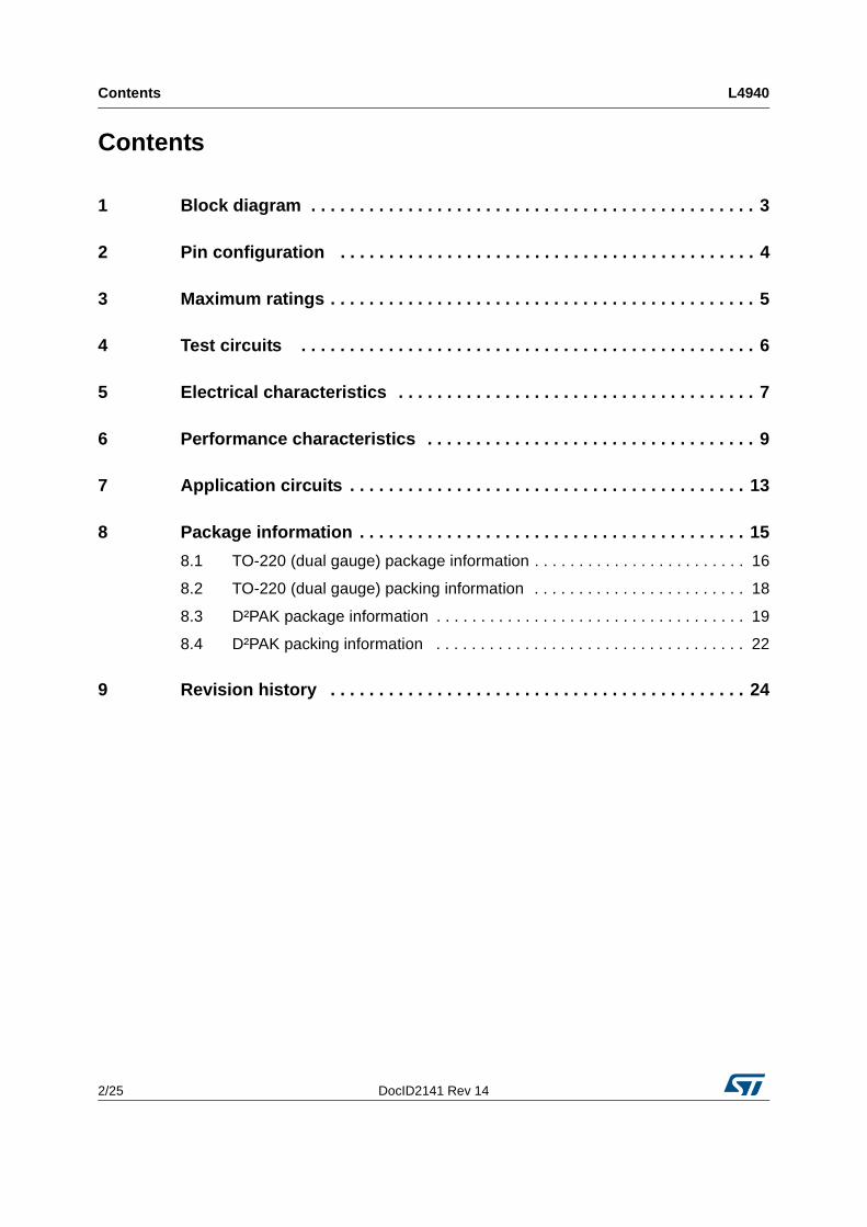
1 Block diagram
Figure 1. Block diagram
Pin configuration L4940
4/25 DocID2141 Rev 14
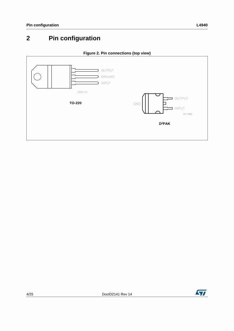
2 Pin configuration
Figure 2. Pin connections (top view)
D²PAK
TO-220
DocID2141 Rev 14 5/25
L4940 Maximum ratings
25
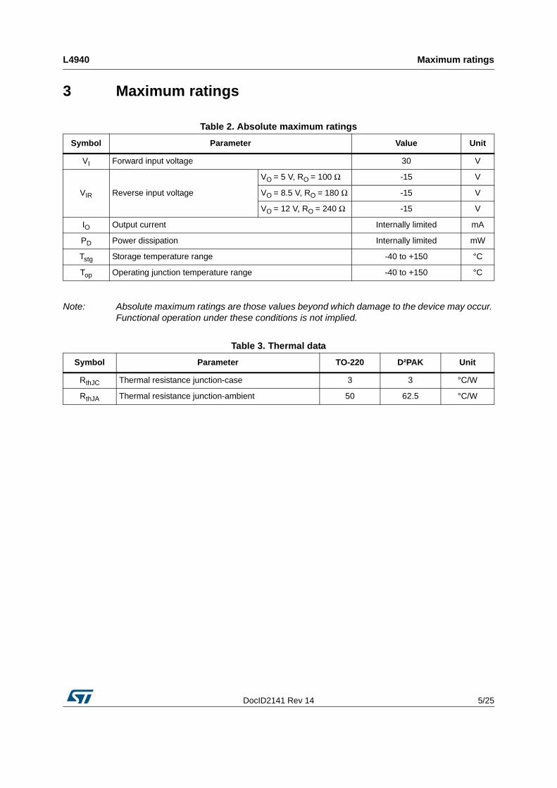
3 Maximum ratings
Note: Absolute maximum ratings are those values beyond which damage to the device may occur. Functional operation under these conditions is not implied.
Table 2. Absolute maximum ratings
Symbol Parameter Value Unit
VI Forward input voltage 30 V
VIR Reverse input voltage
VO = 5 V, RO = 100 Ω -15 V
VO = 8.5 V, RO = 180 Ω -15 V
VO = 12 V, RO = 240 Ω -15 V
IO Output current Internally limited mA
PD Power dissipation Internally limited mW
Tstg Storage temperature range -40 to +150 °C
Top Operating junction temperature range -40 to +150 °C
Table 3. Thermal data
Symbol Parameter TO-220 D²PAK Unit
RthJC Thermal resistance junction-case 3 3 °C/W
RthJA Thermal resistance junction-ambient 50 62.5 °C/W
Test circuits L4940
6/25 DocID2141 Rev 14
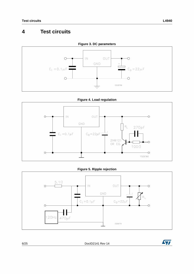
4 Test circuits
Figure 3. DC parameters
Figure 4. Load regulation
Figure 5. Ripple rejection
DocID2141 Rev 14 7/25
L4940 Electrical characteristics
25
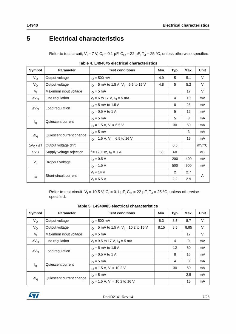
5 Electrical characteristics
Refer to test circuit, VI = 7 V, CI = 0.1 µF, CO = 22 µF, TJ = 25 °C, unless otherwise specified.
Refer to test circuit, VI = 10.5 V, CI = 0.1 µF, CO = 22 µF, TJ = 25 °C, unless otherwise specified.
Table 4. L4940#5 electrical characteristics
Symbol Parameter Test conditions Min. Typ. Max. Unit
VO Output voltage IO = 500 mA 4.9 5 5.1 V
VO Output voltage IO = 5 mA to 1.5 A, VI = 6.5 to 15 V 4.8 5 5.2 V
VI Maximum input voltage IO = 5 mA 17 V
ΔVO Line regulation VI = 6 to 17 V, IO = 5 mA 4 10 mV
ΔVO Load regulationIO = 5 mA to 1.5 A 8 25 mV
IO = 0.5 A to 1 A 5 15 mV
Iq Quiescent currentIO = 5 mA 5 8 mA
IO = 1.5 A, VI = 6.5 V 30 50 mA
ΔIq Quiescent current changeIO = 5 mA 3 mA
IO = 1.5 A, VI = 6.5 to 16 V 15 mA
ΔVO / ΔT Output voltage drift 0.5 mV/°C
SVR Supply voltage rejection f = 120 Hz, IO = 1 A 58 68 dB
Vd Dropout voltageIO = 0.5 A 200 400 mV
IO = 1.5 A 500 900 mV
Isc Short-circuit currentVI = 14 V 2 2.7
AVI = 6.5 V 2.2 2.9
Table 5. L4940#85 electrical characteristics
Symbol Parameter Test conditions Min. Typ. Max. Unit
VO Output voltage IO = 500 mA 8.3 8.5 8.7 V
VO Output voltage IO = 5 mA to 1.5 A, VI = 10.2 to 15 V 8.15 8.5 8.85 V
VI Maximum input voltage IO = 5 mA 17 V
ΔVO Line regulation VI = 9.5 to 17 V, IO = 5 mA 4 9 mV
ΔVO Load regulationIO = 5 mA to 1.5 A 12 30 mV
IO = 0.5 A to 1 A 8 16 mV
Iq Quiescent currentIO = 5 mA 4 8 mA
IO = 1.5 A, VI = 10.2 V 30 50 mA
ΔIq Quiescent current changeIO = 5 mA 2.5 mA
IO = 1.5 A, VI = 10.2 to 16 V 15 mA
Electrical characteristics L4940
8/25 DocID2141 Rev 14
Refer to test circuit, VI = 14 V, CI = 0.1 µF, CO = 22 µF, TJ = 25 °C, unless otherwise specified.
ΔVO / ΔT Output voltage drift 0.8 mV/°C
SVR Supply voltage rejection f = 120 Hz, IO = 1 A 58 66 dB
Vd Dropout voltageIO = 0.5 A 200 400 mV
IO = 1.5 A 500 900 mV
Isc Short-circuit currentVI = 14 V 2 2.7
AVI = 10.2 V 2.2 2.9
Table 5. L4940#85 electrical characteristics (continued)
Symbol Parameter Test conditions Min. Typ. Max. Unit
Table 6. L4940#12 electrical characteristics
Symbol Parameter Test conditions Min. Typ. Max. Unit
VO Output voltage IO = 500 mA 11.75 12 12.25 V
VO Output voltage IO = 5 mA to 1.5 A, VI = 13.8 to 15 V 11.5 12 12.5 V
VI Maximum input voltage IO = 5 mA 17 V
ΔVO Line regulation VI = 13 to 17 V, IO = 5 mA 3 7 mV
ΔVO Load regulationIO = 5 mA to 1.5 A 15 35 mV
IO = 0.5 A to 1 A 10 25 mV
Iq Quiescent currentIO = 5 mA 4 8 mA
IO = 1.5 A, VI = 13.8 V 30 50 mA
ΔIq Quiescent current changeIO = 5 mA 1.5 mA
IO = 1.5 A, VI = 13.8 to 16 V 10 mA
ΔVO /ΔT Output voltage drift 1.2 mV/°C
SVR Supply voltage rejection f = 120 Hz, IO = 1 A 55 61 dB
Vd Dropout voltageIO = 0.5 A 200 400 mV
IO = 1.5 A 500 900 mV
Isc Short-circuit current VI = 14 V 2 2.7 A
ZO Output impedance f = 120 Hz, IO = 0.5 A 40 mΩ
DocID2141 Rev 14 9/25
L4940 Performance characteristics
25
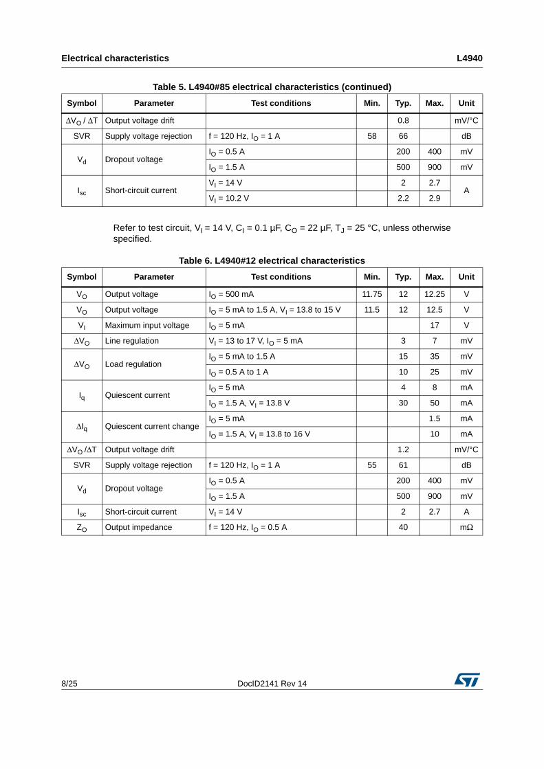
6 Performance characteristics
Figure 6. Dropout voltage vs. output current Figure 7. Dropout voltage vs. temperature
Figure 8. Output voltage vs. temperature (L4940V5)
Figure 9. Output voltage vs. temperature (L4940V85)
Figure 10. Output voltage vs. temperature (L4940V12)
Figure 11. Quiescent current vs. temperature (L4940V5)
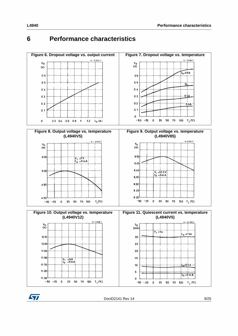
Performance characteristics L4940
10/25 DocID2141 Rev 14
Figure 12. Quiescent current vs. input voltage (L4940V5)
Figure 13. Quiescent current vs. output current (L4940V5)
Figure 14. Short-circuit current vs. temperature (L4940V5)
Figure 15. Peak output current vs. input/output differential voltage (L4940V5)
Figure 16. Low voltage behavior (L4940V5) Figure 17. Low voltage behavior (L4940V85)
DocID2141 Rev 14 11/25
L4940 Performance characteristics
25
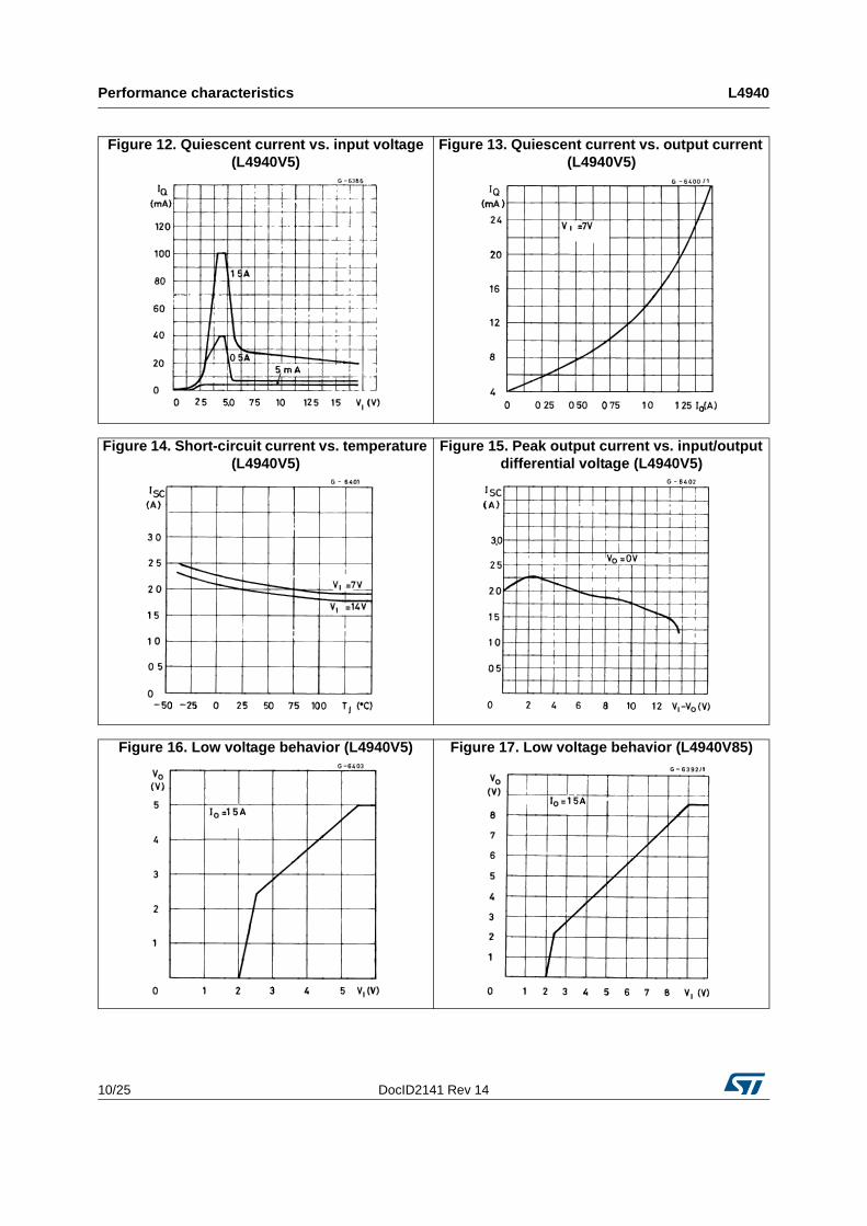
Figure 18. Low voltage behavior (L4940V12) Figure 19. Supply voltage rejection vs. frequency (L4940V5)
Figure 20. Supply voltage rejection vs. output current (L4940V5)
Figure 21. Load dump characteristics (L4940V5)
Figure 22. Line transient response (L4940V5) Figure 23. Total power dissipation
Performance characteristics L4940
12/25 DocID2141 Rev 14
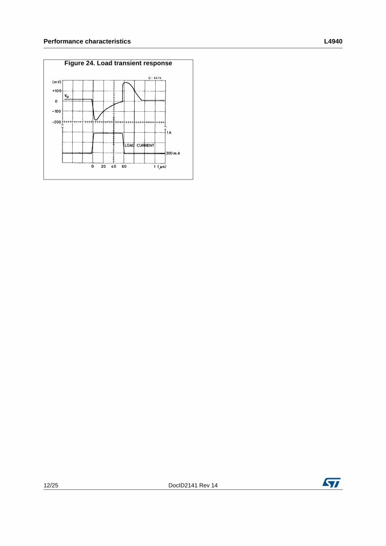
Figure 24. Load transient response
DocID2141 Rev 14 13/25
L4940 Application circuits
25
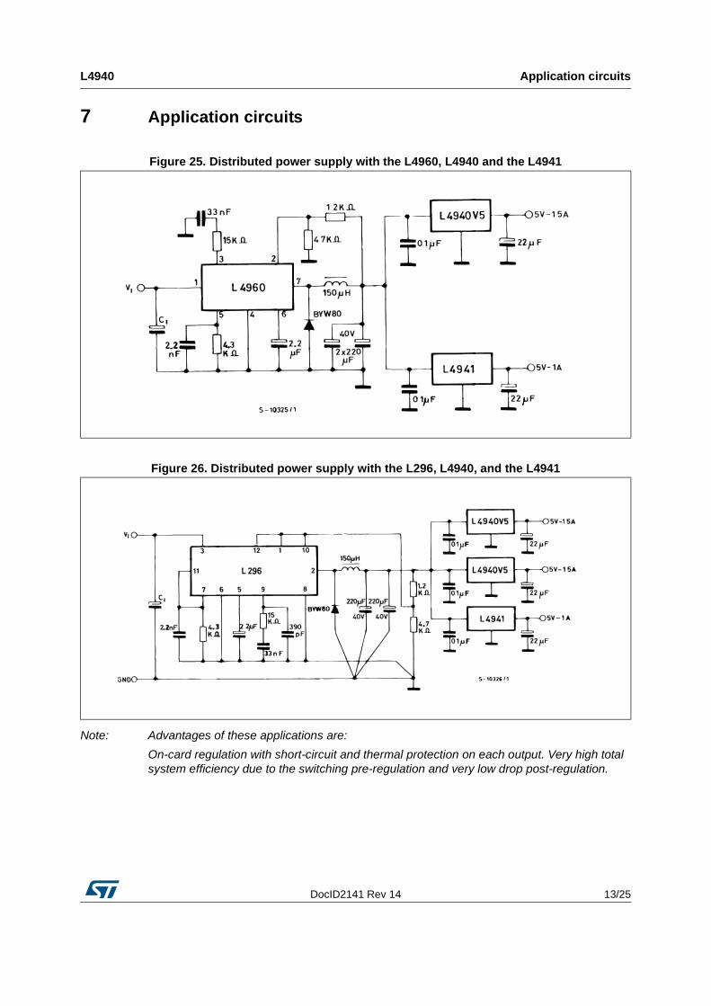
7 Application circuits
Note: Advantages of these applications are:
On-card regulation with short-circuit and thermal protection on each output. Very high total system efficiency due to the switching pre-regulation and very low drop post-regulation.
Figure 25. Distributed power supply with the L4960, L4940 and the L4941
Figure 26. Distributed power supply with the L296, L4940, and the L4941
Application circuits L4940
14/25 DocID2141 Rev 14
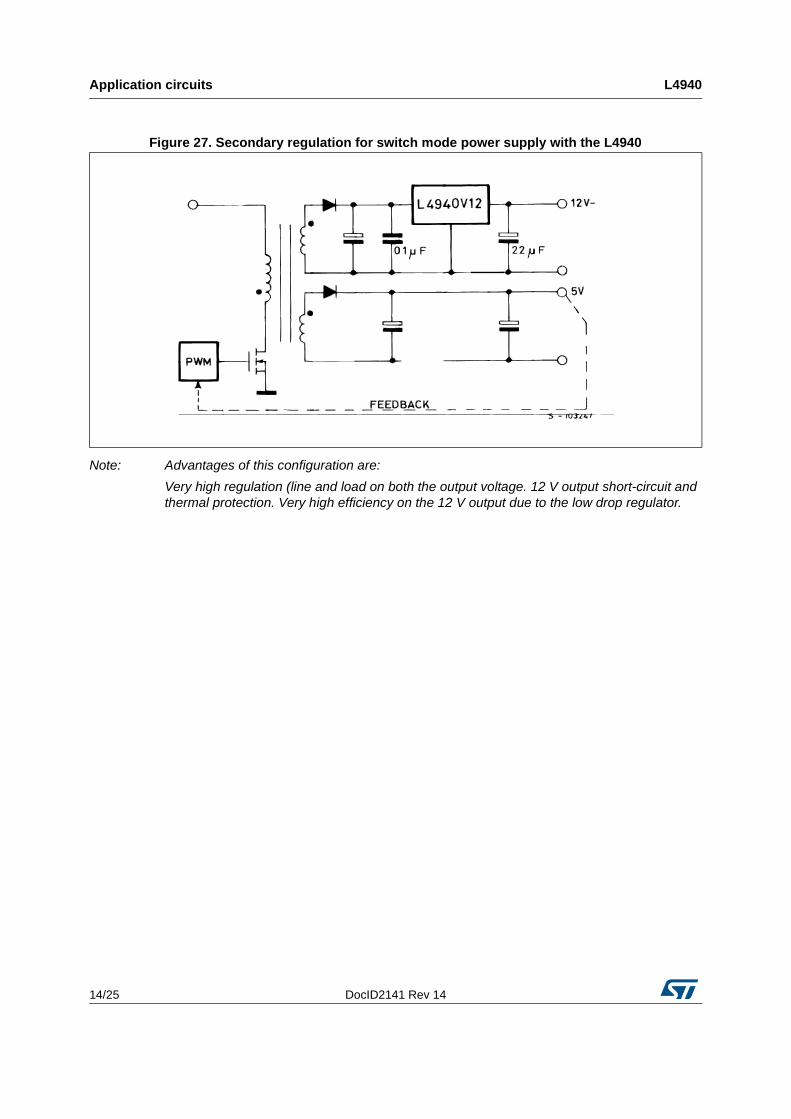
Note: Advantages of this configuration are:
Very high regulation (line and load on both the output voltage. 12 V output short-circuit and thermal protection. Very high efficiency on the 12 V output due to the low drop regulator.
Figure 27. Secondary regulation for switch mode power supply with the L4940
DocID2141 Rev 14 15/25
L4940 Package information
25
8 Package information
In order to meet environmental requirements, ST offers these devices in different grades of ECOPACK® packages, depending on their level of environmental compliance. ECOPACK® specifications, grade definitions and product status are available at: www.st.com. ECOPACK® is an ST trademark.
Package information L4940
16/25 DocID2141 Rev 14
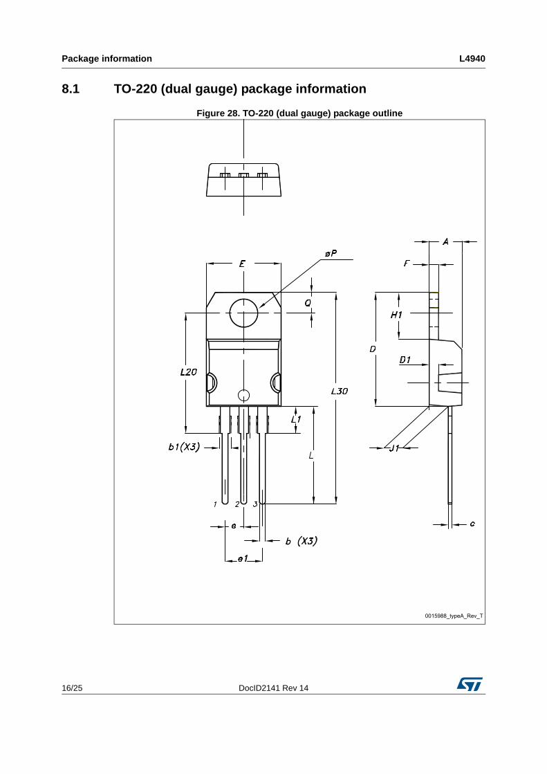
8.1 TO-220 (dual gauge) package information
Figure 28. TO-220 (dual gauge) package outline
DocID2141 Rev 14 17/25
L4940 Package information
25
Table 7. TO-220 (dual gauge) mechanical data
Dim.mm
Min. Typ. Max.
A 4.40 4.60
b 0.61 0.88
b1 1.14 1.70
c 0.48 0.70
D 15.25 15.75
D1 1.27
E 10 10.40
e 2.40 2.70
e1 4.95 5.15
F 1.23 1.32
H1 6.20 6.60
J1 2.40 2.72
L 13 14
L1 3.50 3.93
L20 16.40
L30 28.90
∅P 3.75 3.85
Q 2.65 2.95
Package information L4940
18/25 DocID2141 Rev 14
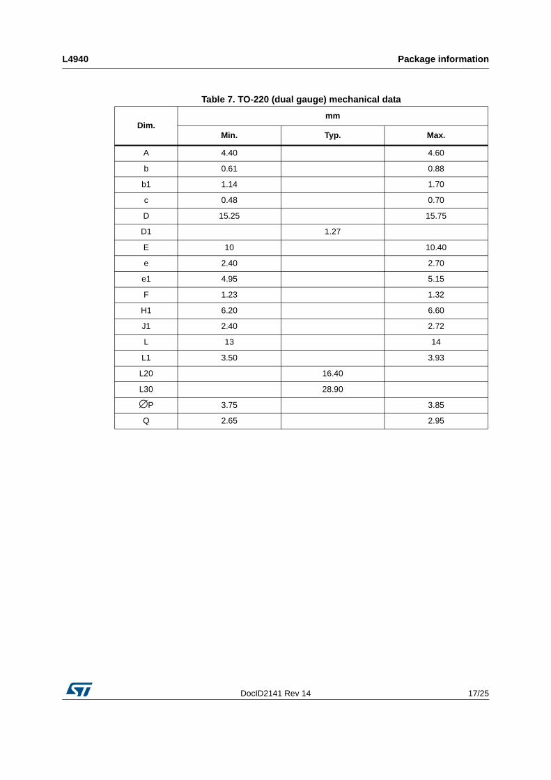
8.2 TO-220 (dual gauge) packing information
Figure 29. Tube for TO-220 (dual gauge) outline (mm.)
DocID2141 Rev 14 19/25
L4940 Package information
25
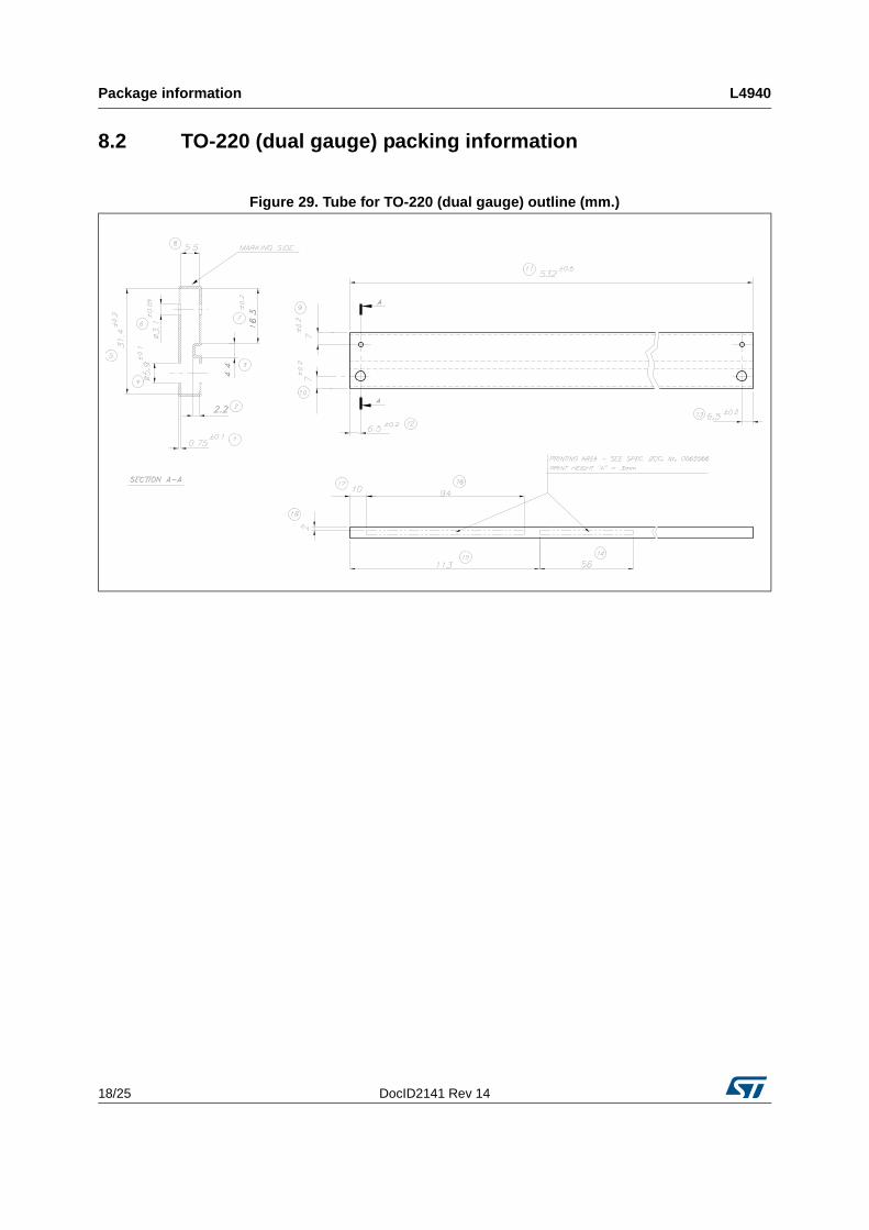
8.3 D²PAK package information
Figure 30. D²PAK package outline
0079457_T
Package information L4940
20/25 DocID2141 Rev 14
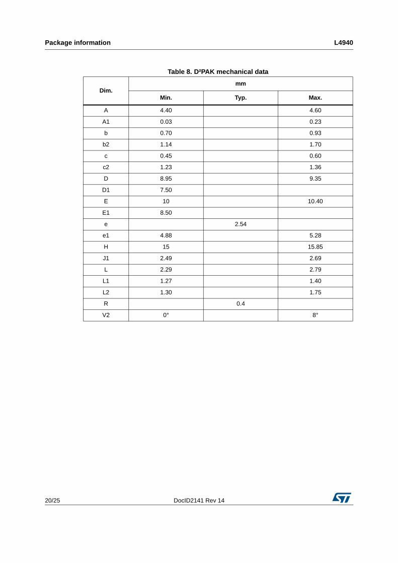
Table 8. D²PAK mechanical data
Dim.mm
Min. Typ. Max.
A 4.40 4.60
A1 0.03 0.23
b 0.70 0.93
b2 1.14 1.70
c 0.45 0.60
c2 1.23 1.36
D 8.95 9.35
D1 7.50
E 10 10.40
E1 8.50
e 2.54
e1 4.88 5.28
H 15 15.85
J1 2.49 2.69
L 2.29 2.79
L1 1.27 1.40
L2 1.30 1.75
R 0.4
V2 0° 8°
DocID2141 Rev 14 21/25
L4940 Package information
25
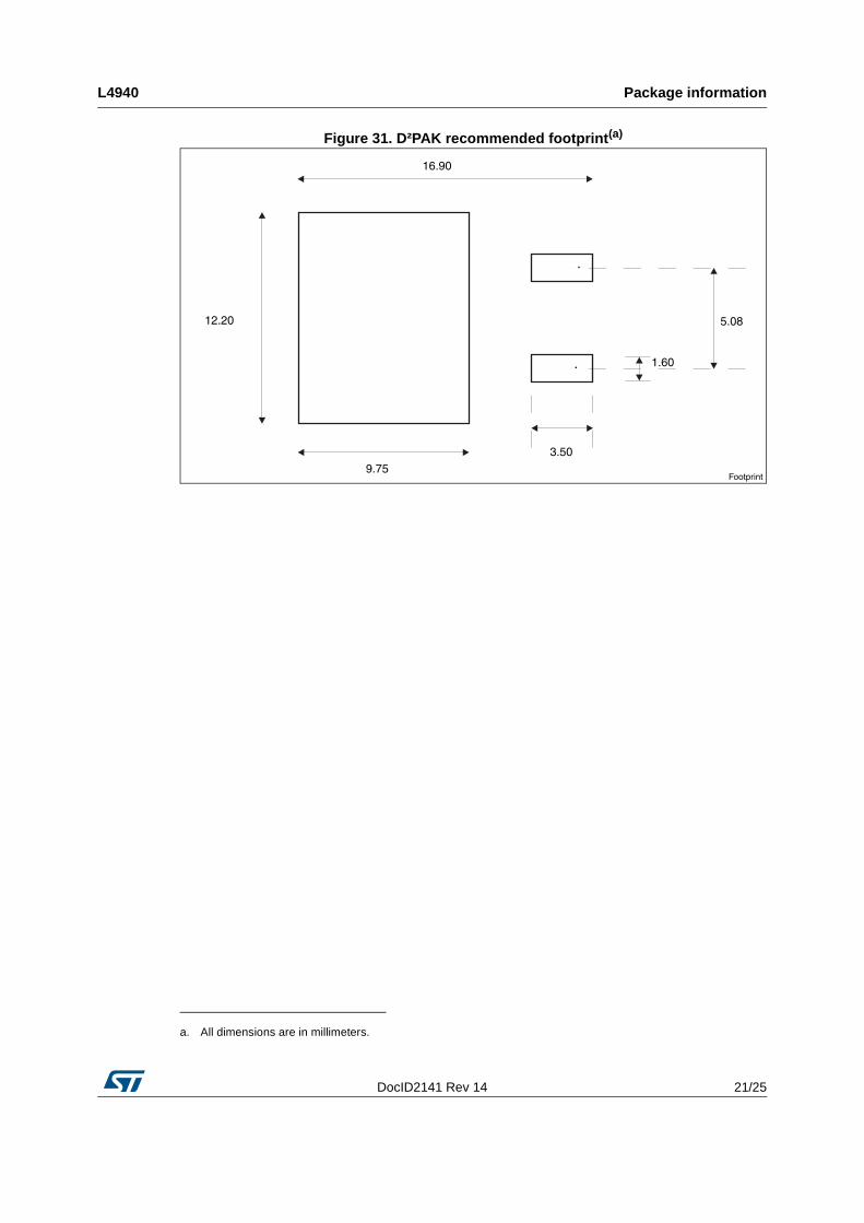
Figure 31. D²PAK recommended footprint(a)
a. All dimensions are in millimeters.
16.90
12.20
9.75
3.50
5.08
1.60
Footprint
Package information L4940
22/25 DocID2141 Rev 14
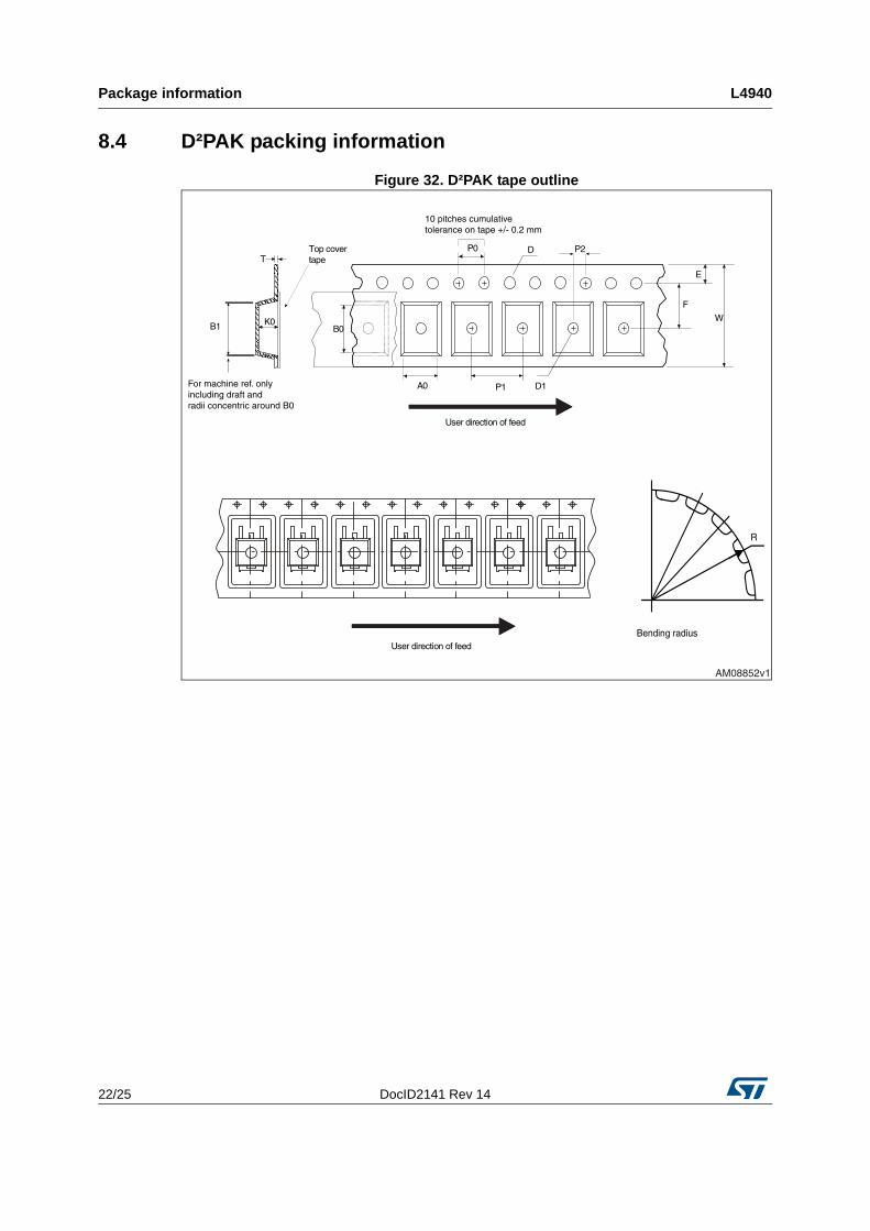
8.4 D²PAK packing information
Figure 32. D²PAK tape outline
P1A0 D1
P0
F
W
E
D
B0K0
T
User direction of feed
P2
10 pitches cumulativetolerance on tape +/- 0.2 mm
User direction of feed
R
Bending radius
B1
For machine ref. onlyincluding draft andradii concentric around B0
AM08852v1
Top covertape
DocID2141 Rev 14 23/25
L4940 Package information
25
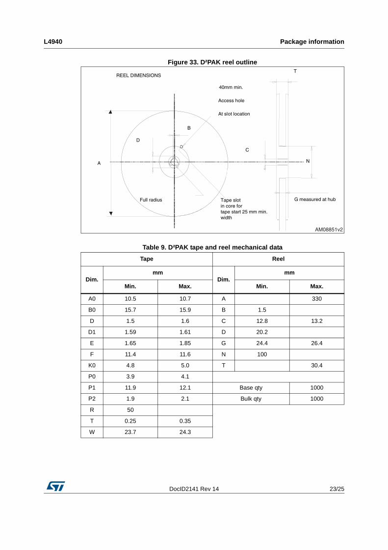
Figure 33. D²PAK reel outline
Table 9. D²PAK tape and reel mechanical data
Tape Reel
Dim.mm
Dim.mm
Min. Max. Min. Max.
A0 10.5 10.7 A 330
B0 15.7 15.9 B 1.5
D 1.5 1.6 C 12.8 13.2
D1 1.59 1.61 D 20.2
E 1.65 1.85 G 24.4 26.4
F 11.4 11.6 N 100
K0 4.8 5.0 T 30.4
P0 3.9 4.1
P1 11.9 12.1 Base qty 1000
P2 1.9 2.1 Bulk qty 1000
R 50
T 0.25 0.35
W 23.7 24.3
A
D
B
Full radius G measured at hub
C
N
REEL DIMENSIONS
40mm min.
Access hole
At slot location
T
Tape slot in core fortape start 25 mm min.width
AM08851v2
Revision history L4940
24/25 DocID2141 Rev 14
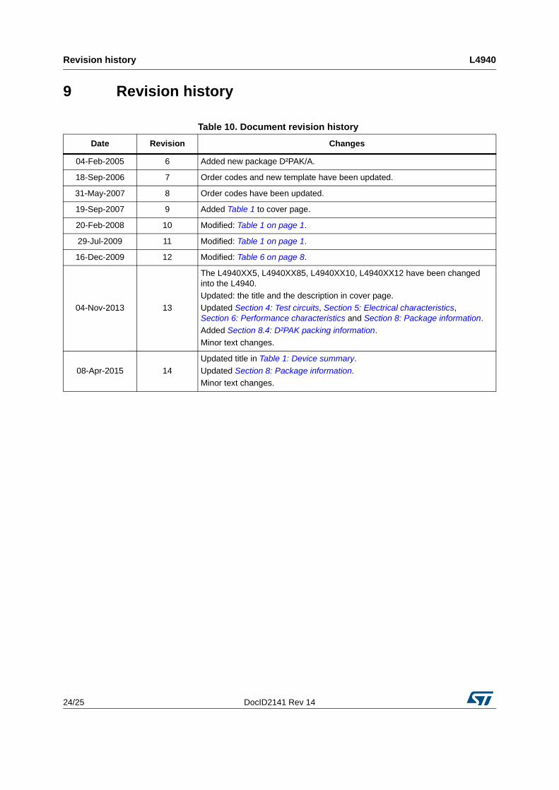
9 Revision history
Table 10. Document revision history
Date Revision Changes
04-Feb-2005 6 Added new package D²PAK/A.
18-Sep-2006 7 Order codes and new template have been updated.
31-May-2007 8 Order codes have been updated.
19-Sep-2007 9 Added Table 1 to cover page.
20-Feb-2008 10 Modified: Table 1 on page 1.
29-Jul-2009 11 Modified: Table 1 on page 1.
16-Dec-2009 12 Modified: Table 6 on page 8.
04-Nov-2013 13
The L4940XX5, L4940XX85, L4940XX10, L4940XX12 have been changed into the L4940.Updated: the title and the description in cover page.Updated Section 4: Test circuits, Section 5: Electrical characteristics, Section 6: Performance characteristics and Section 8: Package information.Added Section 8.4: D²PAK packing information.
Minor text changes.
08-Apr-2015 14
Updated title in Table 1: Device summary.
Updated Section 8: Package information.Minor text changes.
DocID2141 Rev 14 25/25
L4940
25
IMPORTANT NOTICE – PLEASE READ CAREFULLY
STMicroelectronics NV and its subsidiaries (“ST”) reserve the right to make changes, corrections, enhancements, modifications, and improvements to ST products and/or to this document at any time without notice. Purchasers should obtain the latest relevant information on ST products before placing orders. ST products are sold pursuant to ST’s terms and conditions of sale in place at the time of order acknowledgement.
Purchasers are solely responsible for the choice, selection, and use of ST products and ST assumes no liability for application assistance or the design of Purchasers’ products.
No license, express or implied, to any intellectual property right is granted by ST herein.
Resale of ST products with provisions different from the information set forth herein shall void any warranty granted by ST for such product.
ST and the ST logo are trademarks of ST. All other product or service names are the property of their respective owners.
Information in this document supersedes and replaces information previously supplied in any prior versions of this document.
© 2015 STMicroelectronics – All rights reserved