Embed Size (px)
Citation preview

1/5’’ UXGA CMOS Image Sensor GC2035
DataSheet
V1.0
2012-09-18
GalaxyCore Inc.

UXGA CMOS Image Sensor
GC2035 Datasheet 2 / 51
Content
1. SENSOR OVERVIEW ............................................................................................................ 4
1.1 GENERAL DESCRIPTION ............................................................................................................... 4
1.2 FEATURES ................................................................................................................................... 4
1.3 APPLICATION ............................................................................................................................... 5
1.4 TECHNICAL SPECIFICATIONS ........................................................................................................ 5
2. BLOCK DIAGRAM ................................................................................................................. 6
2.1 BLOCK DIAGRAM .......................................................................................................................... 6
2.2 SIGNAL DESCRIPTIONS ................................................................................................................ 7
2.3 PIN DIAGRAM .............................................................................................................................. 8
3. OPTICAL SPECIFICATIONS ............................................................................................... 9
3.1 SENSOR ARRAY CENTER ............................................................................................................... 9
3.2 PIXEL ARRAY ............................................................................................................................. 10
3.3 LENS CHIEF RAY ANGLE (CRA).................................................................................................. 11
3.4 COLOR FILTER SPECTRAL CHARACTERISTICS .............................................................................. 12
4. TWO-WIRE SERIAL BUS COMMUNICATION ................................................................ 12
4.1 PROTOCOL ................................................................................................................................ 12
4.2 SERIAL BUS TIMING ................................................................................................................... 13
5. APPLICATIONS .................................................................................................................... 14
5.1 TIMING DVP ............................................................................................................................. 14
5.2 MIPI ........................................................................................................................................ 15
5.2.1 Clock lane low‐power .......................................................................................................... 15
5.2.2 Data Burst ........................................................................................................................... 16

UXGA CMOS Image Sensor
GC2035 Datasheet 3 / 51
5.3 POWER ON/OFF SEQUENCE ....................................................................................................... 17
5.3.1 Power On Sequence ............................................................................................................ 17
5.3.2 Power Off Sequence ............................................................................................................ 17
5.4 DC PARAMETERS ....................................................................................................................... 17
6. PACKAGE SPECIFICATIONS ............................................................................................. 18
7. REGISTER LIST ................................................................................................................... 19
7.1 SYSTEM REGISTER ..................................................................................................................... 19
7.2 ANALOG & CISCTL ................................................................................................................... 21
7.3 ISP RELATED ............................................................................................................................ 25

UXGA CMOS Image Sensor
GC2035 Datasheet 4 / 51
1. Sensor Overview
1.1 General Description
GC2035 is a high quality 2Mega CMOS image sensor, for mobile phone
camera applications and digital camera products. GC2035 incorporates a 1616V x
1232H pixel array, on-chip 10-bit ADC, and image signal processor.
The on-chip ISP provides a very smooth AE (Auto Exposure) and accurate
AWB (Auto White Balance) control. It provides various data formats, such as
Bayer RGB, RGB565, YCbCr 4:2:2. It has a commonly used two-wire serial
interface for host to control the operation of the whole sensor.
Internal master clock can be generated by on-chip Phase Lock Loop(PLL)
oscillator.
1.2 Features
Standard optical format of 1/5 inch
Various output formats: YCbCr4:2:2, RGB565, Raw Bayer
PLL support
Windowing support
MIPI interface support
Horizontal /Vertical mirror
Image processing module
Package: CSP/wafer

UXGA CMOS Image Sensor
GC2035 Datasheet 5 / 51
1.3 Application
Cellular Phone Cameras
Notebook and desktop PC cameras
PDAs
Toys
Digital still cameras and camcorders
Video telephony and conferencing equipment
Security systems
Industrial and environmental systems
1.4 Technical Specifications
Parameter Typical value
Optical Format 1/5 inch
Pixel Size 1.75um x 1.75um
Active pixel array 1616 x 1232
ADC resolution 10 bit ADC
Shutter type Electronic rolling shutter
Max Frame rate 15fps@24Mhz, UXGA ~30fps@24Mhz, SVGA
Power Supply AVDD28: 2.7~3.0V DVDD18: 1.7~1.9V IOVDD: 1.7~3.0V
Power Consumption 180mW(Active) <100uA(Standby)
SNR TBD
Dark Current TBD
Sensitivity TBD
Operating temperature: -20~70℃
Stable Image temperature 0~50℃
Optimal lens chief ray angle(CRA)
25º(non-linear)
Package type CSP/wafer

UXGA CMOS Image Sensor
GC2035 Datasheet 6 / 51
Image Signal Processing
‐ Interpolation
‐ Denoise
‐ Gamma
‐ Edge enhance
Output
Mode &
Sync
Control
Pixel Array 1616H x 1232V
(1600H x 1200V)
Row Deco
der
Column CDS
Analog Processing
10bit ADC(double)
Timing
Control Configuration
Registers
AWB AEC
HSYNC VSYNC
PCLK
YUV/RGB data
RESET
SCL
MCLK
SDA
2. Block Diagram
2.1 Block Diagram
GC2035 has an active image array of 1616 x 1232 pixels. The active pixels
are read out progressively through column/row driver circuits. In order to reduce
fixed pattern noise, CDS circuits are adopted. The analog signal is transferred to
digital signal by 10 bit A/D converter. The digital signals are processed in the ISP
Block, including Bayer interpolation, de-noise, and color correction, gamma
correction, and data format conversion and so on. Users can easily control these
functions via two-wire serial interface bus.

UXGA CMOS Image Sensor
GC2035 Datasheet 7 / 51
2.2 Signal Descriptions
Name Pin type Description
A1 AVDD28 Power Power for analog circuit/sensor array
A2 PWDN Input power down (active high)
A3 SBCL Input SCCB input clock
A4 VSYNC Output Vertical reference output
A5 PCLK Output Pixel clock output
A6 IOVDD Power Power Supply for I/O circuits
B1 AGND Ground Ground for analog circuit/sensor array
B2 RESETB Input reset (active Low)
B3 SBDA I/O SCCB data
B4 HSYNC Output Horizontal sync output
B5 DVDD18 Power Power for digital core
B6 D<0> Output YUV/RGB video port bit [0]
C1 VPIX Power Internal analog power
C2 TXLOW Power internal analog reference
C3 NC
C4 DGND Ground Ground for digital circuit
C5 D<1> Output YUV/RGB video port bit [1]
C6 D<2> Output YUV/RGB video port bit [2]
D1 CGND Ground Ground for analog circuit
D2 AGND Ground Ground for analog circuit/sensor array
D3 DVDD18 Power Power for digital core
D4 DGND Ground Ground for digital circuit
D5 D<4> Output YUV/RGB video port bit [4]
D6 D<3> Output YUV/RGB video port bit [3]
E1 AVDD28 Power Power for analog circuit/sensor array

UXGA CMOS Image Sensor
GC2035 Datasheet 8 / 51
E2 MDP<0> Output MIPI Data<0> (+)
E3 MDN<1> Output MIPI Data<1> (-)
E4 MCP Output MIPI clock (+)
E5 D<6> Output YUV/RGB video port bit [6]
E6 D<5> Output YUV/RGB video port bit [5]
F1 INCLK Input Sensor master input clock
F2 MDN<0> Output MIPI Data<0> (-)
F3 MDP<1> Output MIPI Data<1> (+)
F4 MCN Output MIPI clock (-)
F5 D<7> Output YUV/RGB video port bit [7]
F6 DVDD18& MVDD
Power Power for digital core
Power for MIPI
2.3 Pin Diagram
Top View

UXGA CMOS Image Sensor
GC2035 Datasheet 9 / 51
3. Optical Specifications
3.1 Sensor Array Center
Top View

UXGA CMOS Image Sensor
GC2035 Datasheet 10 / 51
3.2 Pixel Array
Pixel array is covered by Bayer pattern color filters. The primary color BG/GR
array is arranged in line-alternating way.
If no flip in column, column is read out from 0 to 1615. If flip in column,
column is read out from 1615 to 0.
If no flip in row, row is read out from 0 to 1231. If flip in row, row is read out
from 1231to 0.

UXGA CMOS Image Sensor
GC2035 Datasheet 11 / 51
3.3 Lens Chief Ray Angle (CRA)
Image Height (mm)
Field (%) Image height(mm) CRA(degrees)
0 0 0
10 0.177 4.15
20 0.354 8.25
30 0.531 12.2
40 0.708 15.83
50 0.885 18.98
60 1.062 21.61
70 1.239 23.62
80 1.416 24.82
90 1.593 25.39
100 1.77 25.78
110 1.895 25.89

UXGA CMOS Image Sensor
GC2035 Datasheet 12 / 51
3.4 Color Filter Spectral Characteristics
The optical spectrum of color filters is shown as follows:
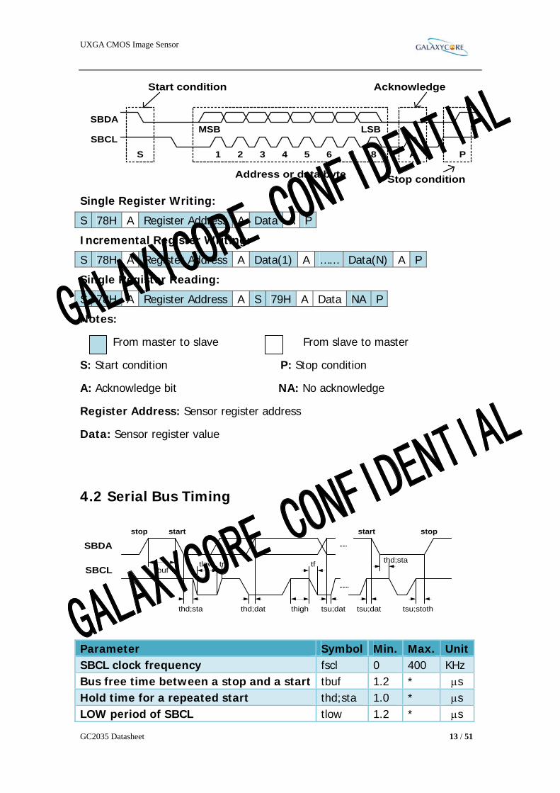
4. Two-wire Serial Bus Communication
GC2035 Device Address:
serial bus write address = 0x78, serial bus read address = 0x79
4.1 Protocol
The host must perform the role of a communications master and GC2035
acts as either a slave receiver or transmitter. The master must do:
Generate the Start(S)/Stop(P) condition
Provide the serial clock on SBCL
UXGA CMOS Image Sensor
GC2035 Datasheet 13 / 51
Single Register Writing:
S 78H A Register Address A Data A P
Incremental Register Writing:
S 78H A Register Address A Data(1) A …… Data(N) A P
Single Register Reading:
S 78H A Register Address A S 79H A Data NA P
Notes:
From master to slave From slave to master
S: Start condition P: Stop condition
A: Acknowledge bit NA: No acknowledge
Register Address: Sensor register address
Data: Sensor register value
4.2 Serial Bus Timing
Parameter Symbol Min. Max. UnitSBCL clock frequency fscl 0 400 KHz Bus free time between a stop and a start tbuf 1.2 * s Hold time for a repeated start thd;sta 1.0 * s LOW period of SBCL tlow 1.2 * s
Start condition Acknowledge
MSB LSB
1 32 4 5 6 7 8
Address or data byte
SBDA
SBCL
A PS
Stop condition
SBDA
SBCL
stop start
thigh
tftrtlow
thd;sta
tbuf
stopstart
thd;dat tsu;dat tsu;dat tsu;stoth
thd;sta

UXGA CMOS Image Sensor
GC2035 Datasheet 14 / 51
HIGH period of SBCL thigh 1.0 * s Set-up time for a repeated start tsu;sta 1.2 * ns Data hold time thd;dat 1.3 * ns Data Set-up time tsu;dat 250 * ns Rise time of SBCL, SBDA tr * 250 ns Fall time of SBCL, SBDA tf * 300 ns Set-up time for a stop tsu;sto 1.2 * s Capacitive load of bus line (SBCL, SBDA) Cb * * pf
5. Applications
5.1 Timing DVP
Supposed Vsync is low active and Hsync is high active, and output format is
YCbCr/RGB565, then the timing of Vsync and Hsync is following:
Ft =VB+ Vt +8(unit is row_time)
VB = Bt + St + Et, Vblank/Dummy line,setting by register 0x07 and 0x08.
Ft -> Frame time, one frame time.
Bt -> Blank time, Vsync no active time.
St -> Start time, setting by register 0x13
Et -> End time, setting by register 0x14
Vt -> valid line time. UXGA is 1200, Vt=win_height-8, win_height is setting
by register 0x0d and 0x0e(1232).
When exp_time <= win_height+VB, Bt=VB-St-Et. Frame rate is controlled
by window_height+VB.
When exp_time > win_height+VB, Bt=exp_time-win_height-St-Et. Frame
rate is controlled by exp_time.
UXGA CMOS Image Sensor
GC2035 Datasheet 15 / 51
The following is row_time calculate:
row_time = Hb + Sh_delay + win_width + 4.
Hb –> HBlank or dummy pixel, Setting by register 0x05 and 0x06.
Sh_delay -> Setting by register 0x11.
win_width -> Setting by register 0x0f and 0x10, win_width = 1600,
final_output_width + 8. So for UXGA, we should set win_width as 1616.
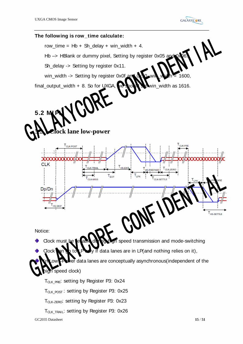
5.2 MIPI
5.2.1 Clock lane low-power
Notice:
Clock must be reliable during high speed transmission and mode-switching
Clock can go to LP only if data lanes are in LP(and nothing relies on it),
In Low –Power data lanes are conceptually asynchronous(independent of the
high speed clock)
TCLK_PRE: setting by Register P3: 0x24
TCLK_POST : setting by Register P3: 0x25
TCLK-ZERO: setting by Register P3: 0x23
TCLK_TRAIL: setting by Register P3: 0x26

UXGA CMOS Image Sensor
GC2035 Datasheet 16 / 51
5.2.2 Data Burst
Notice:
Clock Keeps running and samples data lanes(except for lanes in LPS)
Unambiguous leader and trailer sequences required to distill real ditz,
trailer is removed inside PHY(a few bytes)
Time-out to ignore line values during line state transition
TLPX : setting by Register P3:0x21
THS-PREPARE: setting by Register P3: 0x29
THS-ZERO: setting by Register P3:0x2a
THS-TRAIL: setting by Register P3:0x2b
THS-EXIT: setting by Register P3: 0x27

UXGA CMOS Image Sensor
GC2035 Datasheet 17 / 51
5.3 Power On/Off Sequence
5.3.1 Power On Sequence
5.3.2 Power Off Sequence
5.4 DC Parameters
Symbol Parameter Min Typ Max UnitSupply
VAVDD28 Power supply 2.7 2.8 3.0 V VDVDD18 Supply voltage(digital core) 1.7 1.8 1.9 V VIOVDD Supply voltage(digital I/O) 1.7 1.8 3.0 V IAVDD28
Active(operating) current
30 50 mA IDVDD18 20 100 mA
IIOVDD 1.8V 10 10 mA 2.8V 15 10 mA

UXGA CMOS Image Sensor
GC2035 Datasheet 18 / 51
IDDS_PWD Standby Current 30 60 100 uA Digital Input(Typical conditions: AVDD28 = 2.8V,DVDD = 1.8V,IOVDD = 1.8V) VIH Input voltage HIGH 1.9 V VIL Input voltage LOW 0.5 V Digital Output(AVDD28 = 2.8V,standard Loading 25PF,IOVDD = 1.8V) VOH Output voltage HIGH 2.5 V VOL Output voltage LOW 0.2 V
6. Package Specifications
Description SymbolNominal Min. Max.
Millimeters Package Body Dimension X A 4.570 4.545 4.595
Package Body Dimension Y B 3.840 3.815 3.865
Package Height C 0.780 0.720 0.840
Ball Height C1 0.160 0.130 0.190
Package Body Thickness C2 0.620 0.585 0.655
Thickness from top glass surface to wafer C3 0.445 0.425 0.465
Ball Diameter D 0.300 0.270 0.330
Total Ball Count N 35
Pins Pitch X axis J1 0.730
Pins Pitch Y axis J2 0.600

UXGA CMOS Image Sensor
GC2035 Datasheet 19 / 51
Edge to Pin Center Distance along X S1 0.460 0.430 0.490
Edge to Pin Center Distance along Y S2 0.420 0.390 0.450
7. Register List
7.1 System Register
Address Name Width Default
Value
R/W Description
0xf0 Chip_ID_high 8 0x20 RO ChipIDhighbit
0xf1 Chip_ID_low 8 0x35 RO ChipIDlowbit 0xf2 pad_auto_switch_
mode
sync_pad_io_dvp
pad_vb_hiz_mode
sync_pad_io_ebi
8 0x70 RW [7] pad auto switch mode
[6:4] sync pad io dvp
[3] pad vb hiz mode
[2:0] sync pad io ebi
0xf3 data_pad_io_dvp[
7:0]
8 0xff RW [7:0] data pad io dvp
0xf4 data_pad_io_ebi[7
:0]
8 0x00 RW [7:0] data pad io ebi
0xf5 data_pad_io_dvp[
9:8]
data_pad_io_ebi[9
:8]
6 0x30 RW [5:4] data pad io dvp[9:8]
[1:0] data pad io ebi[9:8]
0xf6 Up_down
Pwd_dn
8 0x00 RW [5:4] updn
00 not pull
01 pull down
10 pull up
11 illegal
[0] PWD dn
0 pull down
1 not pull
0xf7 PLL_mode1 6 0x07 RW [5:4] serial clk double
[3] clk double
[2] Mode 24MHz
[1] div2en
1: divider MCLK 1/2
0: not divider
[0] pll enable
1: enable

UXGA CMOS Image Sensor
GC2035 Datasheet 20 / 51
0: disable
0xf8 PLL_mode2 8 0x00 RW [7] pll dg div enable
[6] NA
[5:0] divx4
0xf9 Cm_mode 8 0xfe RW [7] super clk enable
[6] 2pclk enable
[5] pclk enable
[4] hpclk enable
[3] ISP all clock enable
[2] serial clock enable
[1] re-lock pll
[0] not use pll
0xfa clk_div_mode 8 0x00 RW [7:4] +1 represent the frequency division
number
[3:0]represent the high level in one pulse
after frequency division
Mclk by Div duty
0x11 2 1:1
0x21 3 1:2
0x22 3 2:1
0x31 4 1:3
0x32 4 2:2
0x33 4 3:1
…
0xfb i2c_device_id 7 0x78 RW [7:1] I2C device ID, can write once
[0] NA
0xfc analog_pwc 3 0x06 RW [2] vpix enable
[1] NA
[0] analog pwdn
0xfe Reset related 8 0x00 RW [7] soft reset
[6] SPI receiver reset
[5] NA
[4] restart CISCTL, effective low
[3:2]NA
[1:0] page select
00: registers in REGF0
01: registers in REGF1
10: registers in REGF2
11: registers in REGF3

UXGA CMOS Image Sensor
GC2035 Datasheet 21 / 51
7.2 Analog & CISCTL
Address Name Width Default
Value
R/W Description
P0:0x03 Exposure[12:8] 4 0x00 RO [7:5] NA
[4:0] exposure[12:8],use line processing
time as the unit.
P0:0x04 Exposure[7:0] 8 0x10 RO Exposure[7:0], controlled by AEC if AEC
is in function
P0:0x05 HB[11:8] 4 0x00 RW H Blanking
P0:0x06 HB[7:0] 8 0x94 RW
P0:0x07 VB[12:8] 5 0x00 RW Vertical blanking, if current exposure <
( Vb + window Height) , frame rate will be
( Vb + window Height); otherwise frame
rate will be determined by exposure
P0:0x08 VB[7:0] 8 0x10 RW
P0:0x09 Row_start[10:8] 3 0x00 RW Row Start
P0:0x0a Row_start[7:0] 8 0x00 RW
P0:0x0b Col_start[10:8] 3 0x00 RW Col start
P0:0x0c Col_start[7:1] 8 0x08
P0:0x0d win_height[10:8] 3 0x04 RW [7:2] NA
[2:0] Window height high bit
P0:0x0e win_height[7:0] 8 0xd0 RW Window height low 8 Bit
P0:0x0f win_width[10:8] 3 0x06 RW [7:2] NA
[2:0] Window width high bit
P0:0x10 win_width[7:1] 8 0x50 RW window width low bit
P0:0x11 sh_delay[9:8] 2 0x00 RW [7:3] NA
[2:0] sh_delay[9:8]
P0:0x12 sh_delay[7:0] 8 0x28 RW [7:0] sh_delay[7:0]
P0:0x13 Vs_st 8 0x02 RW Vs_st
P0:0x14 Vs_et 8 0x02 RW for dark row time
P0:0x15 Reserved 8 0x00 RW Reserved
P0:0x16 Reserved 8 0xc1 RW Reserved
P0:0x17 Mirror_updn 8 0X00 RW [7:3] Reserved
[1] Flip
[0] mirror
P0:0x18 Reserved 8 0x0a RW Reserved
P0:0x19 Reserved 8 0x05 RW Reserved
P0:0x1a Reserved 8 0x00 RW Reserved
P0:0x1b Reserved 8 0x44 RW Reserved
P0:0x1c Reserved 8 0x11 RW Reserved

UXGA CMOS Image Sensor
GC2035 Datasheet 22 / 51
P0:0x1d Reserved 8 0x00 RW Reserved
P0:0x1e Reserved 8 0x13 RW Reserved
P0:0x1f Reserved 8 0x00 RW Reserved
P0:0x20 Reserved 8 0x00 RW Reserved
P0:0x21 Reserved 8 0x40 RW Reserved
P0:0x22 Reserved 8 0xb2 RW Reserved
P0:0x23 Reserved 8 0x05 RW Reserved
P0:0x24 PAD_drv 8 0x15 RW [7:6] NA,
[5:4] sync drv
0 0:4mA
0 1:8mA
1 0:12mA
1 1:16mA
[3:2] data drv
0 0:2mA
0 1:4mA
1 0:8mA
1 1:10mA
[1:0] pclk drv
0 0:2mA
0 1:4mA
1 0:8mA
1 1:10mA
P0:0x25 dbrow 8 0x00 RW [7:1] NA
[0] db row
P0:0x3f RC_P
PRC_mode_enabl
e
6 0x11 RW [7:5] RCP[5:0] float 3.3
[1:0] PRC mode enable
[1] postgain RC enable
[0] pregain RC enable
CSI/PHY1.0
Address Name Width Default
Value
R/W Description
P3:0x01 DPHY_analog_mo
de1
8 0x00 RW [6] CTD lane1
[5] CTD lane0
[4] CTD clock
[2] phy lane1 enable
[1] phy lane0 enable
[0] phy clock enable
P3:0x02 DPHY_analog_mo 8 0x00 RW [6:4] lane0 driver

UXGA CMOS Image Sensor
GC2035 Datasheet 23 / 51
de2 [2:0] clock lane driver
P3:0x03 DPHY_analog_mo
de3
8 0x00 RW [6] lane1 delay
[5] lane0 delay
[4] clock delay
[2:0] lane1 driver
P3:0x04 fifo_prog_full_lev
el[7:0]
8 0xa0 RW [7:0] fifo full level[7:0]
P3:0x05 fifo_prog_full_lev
el[11:8]
4 0x00 RW [3:0] fifo full level[11:8]
P3:0x06 fifo_mode 8 0x08 RW [7] MIPI_CLK_MODULE
[6] manual CSI2_up mode
[4] FIFO reset mode
[3] USE_SRAM1_mode
[2] NA
[1] switch read
[0] switch write
P3:0x10 CSI2_mode 8 0x00 RW [7] lane enable
[6] NA
[5] ULP mode
[4] MIPI enable
[3] bit10swicth
[2] RAW8
[1] line sync mode
[0] double lane enable
P3:0x11 LDI_set 8 0x2b RW RAW10
P3:0x12 LWC_set[7:0] 8 0x20 RW [7:0] LWC set[7:0]
P3:0x13 LWC_set[15:8] 8 0x03 RW [7:0] LWC set[15:8]
P3:0x14 SYNC_set 8 0xb8 RW [7:0] SYNC set
P3:0x15 DPHY_mode 8 0x00 RW [7:4] trigger mode
[7] read ready
[6] half
[5] full
[4] programed
[3] PP mode
XOL mode
[2:1] NA
[0] clock lane mode
P3:0x16 LP_set 8 0x09 RW [7:6] hi-z
[3:2] 1
[1:0] 0
P3:0x17 MIPI_wdiv_set 4 0x01 RW default 1/2
P3:0x20 T_init_set 8 0x80 RW more than 100 us

UXGA CMOS Image Sensor
GC2035 Datasheet 24 / 51
P3:0x21 T_LPX_set 8 0x10 RW more than 50ns
P3:0x22 T_CLK_HS_PRE
PARE_set
8 0x05 RW 38ns ~95ns LP00
P3:0x23 T_CLK_zero_set 8 0x30 RW [7:0] T_CLK_PRE_set ,more than 300ns
P3:0x24 T_CLK_PRE_set 8 0x02 RW [7:0] T_CLK_PRE_set ,more than 8UI
P3:0x25 T_CLK_POST_set 8 0x10 RW [7:0] T_CLK_POST_set, 60ns +52UI
P3:0x26 T_CLK_TRAIL_s
et
8 0x08 RW [7:0] T_CLK_TRAIL_set ,60ns
P3:0x27 T_HS_exit_set 8 0x10 RW [7:0] T_HS_exit_set ,more than 100ns
P3:0x28 T_wakeup_set 8 0xa0 RW [7:0] T_wakeup_set ,1ms
P3:0x29 T_HS_PREPARE
_set
8 0x06 RW [7:0] T_HS_PREPARE_set,45+4UI
~85+5UI
P3:0x2a T_HS_Zero_set 8 0x0a RW [7:0] T_HS_Zero_se,140ns
P3:0x2b T_HS_TRAIL_set 8 0x08 RW [7:0] T_HS_TRAIL_set ,60ns
P3:0x30 external_global_m
ode
8 0x03 RW [4] rec dbrow enable flush
[3] EBI dbrow enable
[2] raw data
[1] reg mode
[0] use which edge sample
P3:0x31 external_dvp_mod
e
8 0x00 RW [7] dvp receive enable
[2] dvp decode
[1] dvp10bit
[0] dvp8bit
P3:0x32 external_spi_mode
1
8 0x00 RW [7] spi receive enable
[6] spi1lane2
[5] spi 10 bit
[4] spi 10 bit HL
[3] don’t care reset
[2] no sync
[1:0] bandwidth
P3:0x33 external_spi_mode
2
8 0x01 RW [0] spi msb first
P3:0x34 external_spi_reset
_width
8 0x80 RW External spi reset width
P3:0x35 external_row_start
[15:8]
8 0x00 RW External row start[15:0]
P3:0x36 external_row_start
[7:0]
8 0x00 RW
P3:0x37 external_col_start[
15:8]
8 0x00 RW External col start[15:0]
P3:0x38 external_col_start[ 8 0x00 RW

UXGA CMOS Image Sensor
GC2035 Datasheet 25 / 51
7:0]
P3:0x39 external_win_heig
ht[15:8]
8 0x01 RW External window height[15:0]
P3:0x3a external_win_heig
ht[7:0]
8 0xe8 RW
P3:0x3b external_win_widt
h[15:8]
8 0x02 RW External window width[15:0]
P3:0x3c external_win_widt
h[7:0]
8 0x88 RW
P3:0x3d pad_delay_cnt 8 0x20 RW interval of switch pad
P3:0x3e external_interval 8 0x3f RW External interval
P3:0x3f fifo_error log 8 0x00 RO Fifo error log
P3:0x40 output_buf_mode1 8 0x00 RW [7:4]start mode
[3]NA
[2:1]delay half clk
[0] NA
P3:0x41 output_buf_mode2 8 0x00 RW 2 clk gating
1 pclk polarity
0 hsync polarity
P3:0x42 buf_win_width[7:
0]
8 0x40 RW Buffer window width
P3:0x43 buf_win_width[11
:8]
4 0x06 RW
P3:0x44 buf_win_height[7:
0]
8 0x00 RW Buffer window height
P3:0x45 buf_win_height[10
:8]
3 0x00 RW
7.3 ISP Related
Address Name Width Default
Value
R/W Description
P0:0x80 Block_enable1 8 0x08 RW [7] BKS enable
[6] gamma enable
[5] CC enable
[4] Edge enhancement enable
[3] Interpolation enable
[2] second DN enable
[1] second DD enable
[0] Lens-shading correction enable

UXGA CMOS Image Sensor
GC2035 Datasheet 26 / 51
P0:0x81 Block_enable2 8 0x00 RW [7] NA
[6] low light Y stretch enable
[5] skin detection enable
[4] skin Y enable
[3] new skin mode
[2] autogray enable
[1] Y gamma enable
[0] NA
P0:0x82 AAAA_enable 8 0x00 RW [7] Auto SA enable
[6] auto EE enable
[5] auto DN enable
[4] auto DD enable
[3] auto LSC enable
[2] ABS enable
[1] AWB enable
[0] auto YEE
P0:0x83 Buf_special_effect 8 0x00 RW [7:4] effect select
[3] edge map2
[2] edge map1
[1] fixed CbCr enable
[0] inverse color
P0:0x84 Output_format 8 0x02 RW [7] YUV420rowswitch
[6] YUV420colswitch
[5] shake mode
[4:0] output data mode
5’h00 Cb Y Cr Y
5’h01 Cr Y Cb Y
5’h02 Y Cb Y Cr
5’h03 Y Cr Y Cb
5’h04 LSC bypass, C/Y
5’h05 LSC bypass, Y/C
5’h06 RGB 565
5’h0f bypass 10bits
5’h11 only Y
5’h12 only Cb
5’h13 only Cr
5’h14 only R
5’h15 only G
5’h16 only B
5’h17 switch odd/even column /row to
controls output bayer pattern
0 0 RGBG

UXGA CMOS Image Sensor
GC2035 Datasheet 27 / 51
0 1 RGGB
10 BGGR
11 GBRG
5’h18 DNDD out mode,
5’h19 LSC out mode,
5’h1a pregain out mode
5’h1b EEINTP out mode
P0:0x86 sync_mode 8 0x3f RW Synchronize signal output mode
[7] data delay half
[6] hsync delay half
[5] allow pclk around hsync
[4] allow pclk around vsync
[3] opclk gated in HB
0: not gated
1: gated
[2] opclk polarity
0: invert of isp_2pclk(isp_pclk)
1: same as isp_2pclk(isp_pclk)
[1] hsync polarity
0: low valid
1: high valid
[0] vsync polarity
0: low valid
1: high valid
P0:0x87 block_enable3 5 0x00 RW [7] middle gamma
[5] second DN enable
[4] second DD enable
[0] auto edge effect
P0:0x89 bypass_mode 8 0x83 RW [7] allow hsync in row tail
[6] single2doublemode
[5] first second switch
[4] YUV420mode
[3] is 8 bit bypass
[2] is10 bit bypass for 8 bit data line FPGA
[1:0] bypass which 8bits from 11bit, in is 8
bit bypass mode
11: [10:3]----default
10: [9:2]
01: [8:1]
00: [7:0]
P0:0x8a Clock gating 8 0x81 RW Reserved
P0:0x8b debug_mode1 8 0xac RW [7:6] BFF gate mode

UXGA CMOS Image Sensor
GC2035 Datasheet 28 / 51
[5:4] YUV BFF gate mode
[3:2] pipe gate mode
[1] AWB gain mode
[0] hide_2_clk_mode
P0:0x8c debug_mode2 8 0x00 RW [7] low light Y ratio
[6] skin Y Map
[5] skin show halo mode
[4] skin map
[3] test image mode
1: UXGA
0: VGA
[2] input test image
[1] LSC test image
[0] test image after EEINP
P0:0x8d Debug_mode3 8 0x01 RW [7:4] test image fix value
[3] test image fix value mode
[2] close INBF clock
[1] NA
[0] update gain mode
P0:0x8e Bayer_mode 8 0x18 RW [7] YUV420_legacy_mode
[6] odd even row switch
[5] odd even column switch
[4:0] out count limit
P0:0x90 win_mode_buf 1 0x00 RW [7:1] NA
[0] Crop out Window mode
P0:0x91 Crop_win
_y1[11:0]
High 4 0x00 RWCrop_win_y1
P0:0x92 Low 8 0x00 RW
P0:0x93 Crop_win
_x1[11:0]
High 4 0x00 RWCrop_win_x1
P0:0x94 Low 8 0x00 RW
P0:0x95 out_win_h
eight[10:0]
High 3 0x04 RW Out window height[10:8]
P0:0x96 Low 8 0Xb0 RW Out window height[7:0]
P0:0x97 out_win_
width[10:0
]
High 3 0x06 RW Out window width[10:8]
P0:0x98 Low 8 0x40 RW Out window width[7:0]
P0:0x99 subsample 8 0x11 RW [7:4]subsample row ratio
[3:0]subsample col ratio
P0:0x9a Sub_mode 6 0x06 RW [5] use or cut row
[4] use or cut col
[3] smooth Y
[2] smooth Chroma
[1] neighbor average mode
[0] subsample extend opclk

UXGA CMOS Image Sensor
GC2035 Datasheet 29 / 51
P0:0x9b Sub_row_N1 8 0x02 RW [7:4] subrownum1
[3:0] subrownum2
P0:0x9c Sub_row_N2 8 0x04 RW [7:4] subrownum3
[3:0] subrownum4
P0:0x9d Sub_row_N3 8 0x00 RW [7:4] subrownum5
[3:0] subrownum6
P0:0x9e Sub_row_N4 8 0x00 RW [7:4] subrownum7
[3:0] subrownum8
P0:0x9f Sub_col_N1 8 0x02 RW [7:4] subcolnum1
[3:0] subcolnum2
P0:0xa0 Sub_col_N2 8 0x04 RW [7:4] subcolnum3
[3:0] subcolnum4
P0:0xa1 Sub_col_N3 8 0x00 RW [7:4] subcolnum5
[3:0] subcolnum6
P0:0xa2 Sub_col_N4 8 0x00 RW [7:4] subcolnum7
[3:0] subcolnum8
P0:0xc8 output_buf_enable
able
Y_scaler_binning_
enable
Y_scaler_enable
Y_scaler_base
7 0x05 RW [6] output buffer enable
[5] Y scalar binning enable
[4] Y scalar enable
[3:0] Y scalar base
4/5/6/7/8, scalar ratio = 2/scalar base
Ratio=0.4,out=640x480
BLK
Address Name Width Default
Value
R/W Description
P0:0x40 Blk_mode1 8 0x23 RW [7] not smooth
[6:4] BLK smooth speed
[3] piece wise sdark
[2] dark current mode
[1] dark current enable
[0] offset enable
P0:0x41 BLK_mode2 8 0x09 RW Reserved
P0:0x42 BLK limit value 7 0x7f RW [7] NA
[6:0] When Dark data big than it, while get
this to replace it for protect dark data.
low align 11bits
P0:0x43 Black compress
enable
Global offset
7 0x00 RW [7] Black compress enable
[6:0] global offset
P0:0x44 current_G1_offset 7 0x74 RO [7] NA

UXGA CMOS Image Sensor
GC2035 Datasheet 30 / 51
_odd_offset1 [6:0] current G1 offset odd offset1
P0:0x45 current_G1_offset
_even_offset1
7 0x7c RO [7] NA
[6:0] current G1 offset even offset1
P0:0x46 current_R1_offset
_odd_offset1
7 0x7c RO [7] NA
[6:0] current R offset odd offset1
P0:0x47 current_R1_offset
_even_offset1
7 0x7c RO [7] NA
[6:0] current R offset even offset1
P0:0x48 current_B2_offset
_odd_offset1
7 0x7c RO [7] NA
[6:0] current B offset odd offset1
P0:0x49 current_B2_offset
_even_offset1
7 0x7c RO [7] NA
[6:0] current B offset even offset1
P0:0x4A current_G2_offset
_odd_offset1
7 0x7c RO [7] NA
[6:0] current G2 offset odd offset1
P0:0x4B current_G2_offset
_even_offset1
7 0x7c RO [7] NA
[6:0] current G2 offset even offset1
P0:0x54 current_G1_offset
_odd_dark_current
7 0x3f RO [7] NA
[6:0] current G1 offset odd dark current
P0:0x55 current_G1_offset
_even_dark_curre
nt
7 0x3b RO [7] NA
[6:0] current G1offset even dark current
P0:0x56 current_R1_offset
_odd_dark_current
7 0x44 RO [7] NA
[6:0] current R1offset odd dark current
P0:0x57 current_R1_offset
_even__dark_curr
ent
7 0x40 RO [7] NA
[6:0] current R1offset even dark current
P0:0x58 current_B2_offset
_odd_dark_current
7 0x45 RO [7] NA
[6:0] current B1offset odd offset2
P0:0x59 current_B2_offset
_even_dark_curre
nt
7 0x41 RO [7] NA
[6:0] current B1offset even dark current
P0:0x5a current_G2_offset
_odd_dark_current
7 0x3f RO [7] NA
[6:0] current G2offset odd dark current
P0:0x5b current_G2_offset
_even_dark_curre
nt
7 0x3c RO [7] NA
[6:0] current G2offset even dark current
P0:0x5c Exp_rate_darkc 8 0x04 RW Exp rate darkc
P0:0x5d Offset_sub_
mode
Darkc_submode
8 0x00 RW [7:4] Offset sub mode
[3:0] Darkc sub mode
P0:0x5e offset_ratio_G1_o
dd_temp
6 0x16 RW [7:6]NA
[5:0] 1.5bits offset_ratio_G1_odd

UXGA CMOS Image Sensor
GC2035 Datasheet 31 / 51
P0:0x5f offset_ratio_G1_e
ven_temp
6 0x16 RW [7:6]NA
[5:0] 1.5bits offset_ratio_G1_even
P0:0x60 offset_ratio_R1_o
dd_temp
6 0x16 RW [7:6]NA
[5:0] 1.5bits offset ratio R odd
P0:0x61 offset_ratio_R1_e
ven_temp
6 0x16 RW [7:6]NA
[5:0] 1.5bits offset ratio R even
P0:0x62 offset_ratio_B2_o
dd_temp
6 0x16 RW [7:6]NA
[5:0] 1.5bits offset ratio B odd
P0:0x63 offset_ratio_B2_e
ven_temp
6 0x16 RW [7:6]NA
[5:0] 1.5bits offset ratio B even
P0:0x64 offset_ratio_G2_o
dd_temp
6 0x16 RW [7:6]NA
[5:0] 1.5bits offset ratioG2odd
P0:0x65 offset_ratio_G2_e
ven_temp
6 0x16 RW [7:6]NA
[5:0] 1.5bits offset ratioG2even
P0:0x66 Dark_current_
G1_ ratio
6 0x18 RW [7:6]NA
[5:0] 1.5bits dark current ratioG1
P0:0x67 Dark_current_R1_
ratio
6 0x18 RW [7:6]NA
[5:0] 1.5bits dark current ratio R
P0:0x68 Dark_current_B2_
ratio
6 0x18 RW [7:6]NA
[5:0] 1.5bits dark current ratio B
P0:0x69 Dark_current_
G2_ ratio
6 0x18 RW [7:6]NA
[5:0] 1.5bits dark current ratio G2
P0:0x6A manual_G1_odd_o
ffset
6 0x00 RW [7:6] NA
[5:0] S5, aligned to lower 8 of 11 bits data
P0:0x6B manual_G1_
even_offset
6 0x00 RW [7:6] NA
[5:0] S5, aligned to lower 8 of 11 bits data
P0:0x6C manual_R1_odd_o
ffset
6 0x00 RW [7:6] NA
[5:0] S5, aligned to lower 8 of 11 bits data
P0:0x6D manual_R1_even_
offset
6 0x00 RW [7:6] NA
[5:0] S5, aligned to lower 8 of 11 bits data
P0:0x6E manual_B2_odd_o
ffset
6 0x00 RW [7:6] NA
[5:0] S5, aligned to lower 8 of 11 bits data
P0:0x6F manual_B2_even_
offset
6 0x00 RW [7:6] NA
[5:0] S5, aligned to lower 8 of 11 bits data
P0:0x70 manual_G2_odd_o
ffset
6 0x00 RW [7:6] NA
[5:0] S5, aligned to lower 8 of 11 bits data
P0:0x71 manual_G2_
even_offset
6 0x00 RW [7:6] NA
[5:0]S5, aligned to lower 8 of 11 bits data
P0:0x77 black_compress 8 0xf6 RW [7:4] blackcompresst2
[3:0] blackcompresst1
P0:0x78 Close frame mode 8 0x44 RW [7]NA

UXGA CMOS Image Sensor
GC2035 Datasheet 32 / 51
Close frame num [6:4] close frame mode
[3:0] close frame number
P0:0x79 Close frame num1 8 0x12 RW [7:0] close frame num1
P0:0x7a Close frame num2 8 0x00 RW [7:0] close frame num2
GLOBAL/PRE/POSTGAIN
Address Name Width Default
Value
R/W Description
P0:0xa3 channel_gain_G1_
odd
8 0x80 RW [7:0] G1 odd Channel gain, float 1.7
P0:0xa4 channel_gain_G1_
even
8 0x80 RW [7:0] G1 even Channel gain, float 1.7
P0:0xa5 channel_gain_R1_
odd
8 0x80 RW [7:0] R1 odd Channel gain, float 1.7
P0:0xa6 channel_gain_R1_
even
8 0x80 RW [7:0] R1 even Channel gain, float 1.7
P0:0xa7 channel_gain_B2_
odd
8 0x80 RW [7:0] B2 odd channel gain, float 1.7
P0:0xa8 channel_gain_B2_
even
8 0x80 RW [7:0] B2 even channel gain, float 1.7
P0:0xa9 channel_gain_G2_
odd
8 0x80 RW [7:0] G2 odd channel gain, float 1.7
P0:0xaa channel_gain_G2_
even
8 0x80 RW [7:0] G2 even channel gain, float 1.7
P0:0xad R_ratio 8 0x80 RW [7:0] R ratio 1.7bits, float 1.7
P0:0xae G_ratio 8 0x80 RW [7:0] G ratio 1.7bits, float 1.7
P0:0xaf B_ratio 8 0x80 RW [7:0] B ratio 1.7bits, float 1.7
P0:0xb0 Global_gain 8 0x40 RW Global gain, float 4.4
P0:0xb1 Auto_pregain 8 0x40 RO [7:0] Controlled by AEC , can be manually
controlled when disable AEC
P0:0xb2 Auto_postgain 8 0x40 RO [7:0] Controlled by AEC , can be manually
controlled when disable AEC
P0:0xb3 AWB_R_gain 8 0x40 RO [7:0] AWB R gain float 4.4
P0:0xb4 AWB_G_gain 8 0x40 RO [7:0] AWB G gain float 4.4
P0:0xb5 AWB_B_gain 8 0x40 RO [7:0] AWB B gain float 4.4. controlled by
AWB
DNDD/DITHER
Address Name Width Default
Value
R/W Description

UXGA CMOS Image Sensor
GC2035 Datasheet 33 / 51
P2:0x86 DN mode 8 0x87 RW [7:5] Auto DD mode
[4] zero weight mode
[3] share mode
[2] Reserved
[1] dn lsc mode
[0] Reserved
P2:0x87 DD mode 8 0x22 RW [7:6] bad ratio
[5:4] C weight adaptive ratio
[3:2] dn lsc ratio
[1:0] dn b mode ratio
P2:0x88 DN_auto_disable
DN_bilat_b_base
8 0x15 RW [7] DN auto disable
[6] NA
[5:0] Fixed bilateral b value
P2:0x89 DN_bilat_n_base
DN_C_weight
8 0x05 RW [7:4] DN bilat_n base
[3:0] base center pixel weight
P2:0x8a DD_dark_bright_
TH
8 0x05 RW [7:4] DD dark THD
[3:0] DD bright THD
P2:0x8b DD_flat_TH 8 0x86 RW [7:4] dd th subtract one
[3:0] dd th subtract two
P2:0x8c DD_limit
DN_b_in_dark_in
c_or_dec
DD_ratio
8 0xf2 RW [7:4] DD limit, threshold of a defect pixel
[3] NA
[2] DN datk mode
[1:0] DD ratio
P2:0x8d DN_b_in_dark_
enable
DD_mm_TH
8 0x8a RW [7] DN bin dark enable
[6] DD select weight
[3:0] DD mm TH
P2:0x8e DN_b_in_dark_
th
DN_b_in_dark_
slope
8 0xff RW [7:4] DN bin dark THD
[3:0] DN bin dark slope
P2:0x8f DN skin mode 5 0x00 RW Reserved
P2:0x9d Reserved 3 0x03 RW Reserved
P2:0x9e Reserved 8 0x00 RW Reserved
INTPEE (Interpolation and Edge Enhancement)
Address Name Width Default
Value
R/W Description
P2:0x90 EEINTP mode 1 8 0x6c RW [7] edge1 mode
[6] new edge mode
[5] edge2 mode
[4] interpolation select mode

UXGA CMOS Image Sensor
GC2035 Datasheet 34 / 51
[3] LP interpolation enable
[2] LP edge enable
[1:0] LP edge mode
P2:0x91 EEINTP mode 2 8 0x00 RW Reserved
P2:0x92 Direction TH1 6 0x08 RW [7:6] NA
[5:0] Lower Criteria for direction detection
P2:0x93 Direction TH2 6 0x03 RW [7:6] NA
[5:0] Upper Criteria for direction detection
P2:0x94 Edge THD 8 0x00 RW Reserved
P2:0x95 direction_diff_TH 8 0x83 RW [3:0] Direction diff TH1
[3:0] Direction diff TH2
P2:0x96 direction_mode 2 0x00 RW direction_mode
P2:0x97 Edge1 effect
Edge2 effect
8 0x48 RW [7:4] edge1 effect
[3:0] edge2 effect
P2:0x98 Edge_pos_ratio
Edge_neg_ratio
8 0x88 RW [7:4] pos edge ratio
[3:0] neg edge ratio
P2:0x99 Edge1_max
Edge1_min
8 0x81 RW [7:4] edge1 max
[3:0] edge1 min
P2:0x9a Edge2_max
Edge2_min
8 0x81 RW [7:4] edge2 max
[3:0] edge2 min
P2:0x9b Edge1_th
Edge2_th
8 0x22 RW [7:4] edge1 threshold
[3:0] edge2 threshold
P2:0x9c Edge_pos_max
Edge_neg_max
8 0xf8 RW [7:4] Positive edge max
[3:0] Negative edge max
ASDE
Address Name Width Default
Value
R/W Description
P2:0xa2 ASDE_LSC_gain_
dec_slope
8 0x80 RW [7:0] LSC gain decrease slope
P2:0xa3 ASDE_low_luma_
value_th
8 0x20 RW [7:0] ASDE Offset dark THD
P2:0xa4 ASDE_low_luma_
value_offset_slope
4 0x02 RW [3:0] ASDE low luminance value offset
slope
P2:0xa5 ASDE_low_luma_
value_LSC_th
8 0x20 RW [7:0] ASDE LSC dark THD
P2:0xa6 ASDE_low_luma_
value_DD_th
8 0x20 RW [7:0] ASDE DD dark THD
P2:0xa7 ASDE_low_luma_
value_OT_th
8 0x20 RW [7:0] ASDE OT dark THD
P2:0xa9 ASDE DN b 8 0x66 RW Reserved
UXGA CMOS Image Sensor
GC2035 Datasheet 35 / 51
P2:0xaa ASDE DN c 8 0xaa RW Reserved
P2:0xab DN&EEINTP
mode
8 0x00 RW Reserved
P2:0xac Reserved 6 0x15 RO Reserved
P2:0xad Reserved 5 0x10 RO Reserved
P2:0xae ASDE_DD_bright
_th_slope
ASDE_DD_limit_
slope
8 0x5f RW [7:4] ASDE DD bright Thd slope
[3:0] ASDE DD limit slope
P2:0xaf ASDE_DD_bright
_th
ASDE_DD_limit
8 0x5f RO [7:4] ASDE DD bright THD
[3:0] ASDE DD limit
P2:0xb0 ASDE EE low 8 0x12 RW Reserved
P2:0xb1 ASDE EE1 high 8 0x12 RW Reserved
P2:0xb2 ASDE edge effect 8 0x48 RO [7:4] ASDE_edge1_effect
[3:0] ASDE_edge2_effect
P2:0xb3 ASDE_auto_satur
ation_dec_slope
8 0x10 RW [7:4] Auto saturation decrease slope
Float 6.2bit
P2:0xb4 ASDE_auto_satur
ation_low_limitAS
DE_sub_saturation
_slope
8 Ox31 RW [7:4] ASDE auto saturation low limit
[3:0] ASDE sub saturation slope
P2:0xb5 ASDE_DD_mm_t
h_slope
4 0xaa RW [7:0] ASDE DD mm THD slope
P2:0x48 Reserved 8 0x04 RW Reserved
P2:0x49 Reserved 8 0x01 RW Reserved
P2:0x4a Reserved 8 0x79 RO Reserved
P2:0x38 auto_gray_dec_slo
pe
4 0x08 RW [3:0] autogray decrease slope
P2:0x39 auto_gray_dec_th 8 0x40 RW Autograydecth
P2:0x3a Reserved 8 0x10 RO Reserved
P1:0xec Reserved 8 0x03 RO Reserved
AUTO_CC
Address Name Width Default
Value
R/W Description
P2:0xc0 CC_mode 8 0x00 RW [7:6] NA
[5:4] CCT mode
[3:1] NA
[0] CCT enable
P2:0xc1 CC_CT1_11 8 0x40 RW D-light cc

UXGA CMOS Image Sensor
GC2035 Datasheet 36 / 51
RGB GAMMA
Address Name Width Default
Value
R/W Description
P2:0x15 Gamma_out1 8 0x0a RW Each out value of knee i. Knee0=2
P2:0x16 Gamma_out2 8 0x12 RW Knee1=4
P2:0x17 Gamma_out3 8 0x19 RW Knee2=6
P2:0x18 Gamma_out4 8 0x1f RW Knee3=8
P2:0x19 Gamma_out5 8 0x2c RW Knee4=12
P2:0x1a Gamma_out6 8 0x38 RW Knee5=16
P2:0x1b Gamma_out7 8 0x42 RW Knee6=20
P2:0x1c Gamma_out8 8 0x4e RW Knee7=24
P2:0x1d Gamma_out9 8 0x63 RW Knee8=32
P2:0x1e Gamma_out10 8 0x76 RW Knee9=40
P2:0x1f Gamma_out11 8 0x87 RW Knee10=48
P2:0x20 Gamma_out12 8 0x96 RW Knee11=56
P2:0x21 Gamma_out13 8 0xa2 RW Knee12=64
P2:0x22 Gamma_out14 8 0xb8 RW Knee13 =80
P2:0x23 Gamma_out15 8 0xca RW Knee14 = 96
P2:0x24 Gamma_out16 8 0xd8 RW Knee15 = 112
P2:0x25 Gamma_out17 8 0xe3 RW Knee16 = 128
P2:0x26 Gamma_out18 8 0xf0 RW Knee17 =160
P2:0x27 Gamma_out19 8 0xf8 RW Knee18 = 192
P2:0xc2 CC_CT1_12 8 0x00 RW
P2:0xc3 CC_CT1_13 8 0x00 RW
P2:0xc4 CC_CT1_21 8 0x00 RW
P2:0xc5 CC_CT1_22 8 0x40 RW
P2:0xc6 CC_CT1_23 8 0x00 RW
P2:0xc7 CC_CT2_11 8 0x40 RW Cwf-light,TL84-light cc
P2:0xc8 CC_CT2_12 8 0x00 RW
P2:0xc9 CC_CT2_13 8 0x00 RW
P2:0xca CC_CT2_21 8 0x00 RW
P2:0xcb CC_CT2_22 8 0x40 RW
P2:0xcc CC_CT2_23 8 0x00 RW
P2:0xcd CC_CT3_11 8 0x40 RW A-light,U30-light cc
P2:0xce CC_CT3_12 8 0x00 RW
P2:0xcf CC_CT3_13 8 0x00 RW
P2:0xe3 CC_CT3_21 8 0x00 RW
P2:0xe4 CC_CT3_22 8 0x40 RW
P2:0xe5 CC_CT3_23 8 0x00 RW

UXGA CMOS Image Sensor
GC2035 Datasheet 37 / 51
P2:0x28 Gamma_out20 8 0xfd RW Knee19 = 224
P2:0x29 Gamma_out21 8 0xff RW Knee20 = 256
Y GAMMA
Address Name Width Default
Value
R/W Description
P2:0x2b Y_Gamma_out0 8 0x00 RW Each out value of knee i. Knee0=0
P2:0x2c Y_Gamma_out1 8 0x10 RW Knee1=8
P2:0x2d Y_Gamma_out2 8 0x1c RW Knee2=16
P2:0x2e Y_Gamma_out3 8 0x30 RW Knee3=32
P2:0x2f Y_Gamma_out4 8 0x43 RW Knee4=48
P2:0x30 Y_Gamma_out5 8 0x54 RW Knee5=64
P2:0x31 Y_Gamma_out6 8 0x65 RW Knee6=80
P2:0x32 Y_Gamma_out7 8 0x75 RW Knee7=96
P2:0x33 Y_Gamma_out8 8 0x93 RW Knee8=128
P2:0x34 Y_Gamma_out9 8 0xb0 RW Knee9=160
P2:0x35 Y_Gamma_out1
0
8 0xcb RW Knee10=192
P2:0x36 Y_Gamma_out1
1
8 0xe6 RW Knee11=224
P2:0x37 Y_Gamma_out1
2
8 0xff RW Knee12=256
YCP
Address Name Width Default
Value
R/W Description
P2:0xd0 Global saturation 8 0x40 RW [7:0] Global saturation, controlled by
auto saturation
P2:0xd1 saturation_Cb 8 0x30 RW [7:0] Cb saturation
3.5bits, 0x20=1.0
P2:0xd2 saturation_Cr 8 0x30 RW [7:0] Cr saturation
3.5bits, 0x20=1.0
P2:0xd3 luma_contrast 8 0x40 RW [7:0] Luma contrast
P2:0xd4 Contrast center 8 0x80 RW [7:0] Contrast center value
P2:0xd5 Luma_offset 8 0x00 RW [7:0] Add offset on luma value. S7.
P2:0xd6 skin_Cb_center 8 0xec RW [7:0] Cb criteria for skin detection.
P2:0xd7 skin_Cr_center 4 0x12 RW [7:0] Cr criteria for skin detection.
P2:0xd8 Skin radius
square
6 0x10 RW [7:0] Defines skin range
P2:0xd9 Skin brightness 8 0xe3 RW [7:4] skin brightness high threshold

UXGA CMOS Image Sensor
GC2035 Datasheet 38 / 51
[3:0] skin brightness low threshold
P2:0xda Fixed_Cb 8 0x00 RW S7, if fixed CbCr function is enabled,
current image Cb value will be replace
by this value to achieve special effect
P2:0xdb Fixed_Cr 8 0x00 RW S7, if fixed CbCr function is enabled,
current image Cr value will be replace
by this value to achieve special effect
P2:0xdc exp_under_sun_t
h
8 0x32 RW Exp under sun THD
P2:0xdd Edge sa-mode 8 0x08 RW [7] under sun mode
[6:4] edge saturation enable
[3:0] edge saturation slope
P2:0xde Asde autogray
mode
8 0x38 RW [7] asde auto gray enable
[6] NA
[5:4] sa autogray mode
[3:0] sa autogray
P2:0xdf saturation_sub_st
rength
8 0x00 RO
P2:0xe0 skin_bright_cent
er
5 0x0f RW Skin bright center
P2:0xe1 Y_delta 5 0x18 RW Gt than 0x18
P2:0xe2 Skin_RR_halo_r
adius
6 0x20 RO Chroma offset in low light
Gt than 0x10
P2:0xe7 center_U 8 0xe8 RW Amplitude of skin correction towards Cb
P2:0xe8 center_V 8 0x1f RW Amplitude of skin correction towards Cr
P2:0xea U_bius_div_Rad
ius
8 0x2b RW U bius div Radius
P2:0xeb V_bius_div_Rad
ius
8 0x14 RW V bius div Radius
P2:0xec Skin__mode 4 0x03 RW Reserved
Measure Window
Address Name Width Default
Value
R/W Description
P0:0xec big_win_x0 8 0x04 RW
Big win use by AEC and AWB P0:0xed big_win_y0 8 0x02 RW
P0:0xee big_win_x1 8 0x60 RW
P0:0xef big_win_y1 8 0x90 RW
AEC

UXGA CMOS Image Sensor
GC2035 Datasheet 39 / 51
Address Name Width Default
Value
R/W Description
P0:0xb6 AEC_up_enable
AEC_enable
2 0x00 RW [7:2] NA
[1] AEC up enable
[0] AEC enable
P1:0x01 aec_x1 8 0x04 RW [7:0] X16 local measure window
P1:0x02 aec_x2 8 0x60 RW [7:0] X16 local measure window
P1:0x03 aec_y1 8 0x02 RW [7:0] aec_y1, X8
P1:0x04 aec_y2 8 0x90 RW [7:0] aec_y2,X8
P1:0x05 aec_center_x1 8 0x20 RW [7:0] aec_center_x1, X16
P1:0x06 aec_center_x2 8 0x40 RW [7:0] aec_center_x2,X16
P1:0x07 aec_center_y1 8 0x40 RW [7:0] aec_center_y1,X8
P1:0x08 aec_center_y2 8 0x60 RW [7:0] aec_center_y2,X8
P1:0x09 AEC_mode 8 0x40 RW [7] Reserved
P1:0x0a AEC_mode1 8 0x01 RW [7] low light mode,
[6] measure point
[5] exposure mode
[4] fix frame rate mode
[3:2] EC parameters
[1:0] skip mode
P1:0x0b AEC_mode2 8 0x21 RW [7] fix target
[6:4] AEC take action every N frame
[3:2] close frame number to eliminate
bad frame
[1] change exposure gain mode
[0] Reserved
P1:0x0c AEC_mode3 8 0x01 RW [7] map measure point
[6:4] center weight mode
[3:2] skin weight mode
[1] raw skip mode
[0] fix target high
P1:0x0d AEC_mode4 8 0x00 RW [7] new exposure mode
[6:4] new exposure mode index
[3:0] Reserved
P1:0x0e AEC_thd[7:0] 8 0x40 RW AEC parameters
P1:0x0f AEC_thd[15:8] 8 0x60 RW AEC parameters
P1:0x10 skin_exp_thd 8 0x09 RW Skin mode exposure thd
P1:0x11 AEC_slope 8 0x40 RW AEC Y target slope
P1:0x12 AEC_target_skin 8 0x60 RW AEC target skin
P1:0x13 AEC_target_Y 8 0x50 RW expected luminance value
P1:0x14 Y_average 8 0x80 RO Current frame luminance average

UXGA CMOS Image Sensor
GC2035 Datasheet 40 / 51
P1:0x15 AEC_high_low
_range
8 0xf2 RW [7:4] x16, count limit for high luminance
pixels
[3:0] x4, count limit for low luminance
pixels
P1:0x16 AEC_number_li
mit_high_range
8 0x35 RW AEC number limit high range
P1:0x17 AEC_ignore 8 0x18 RW [7] high luminance limit mode
[6] only center limit mode
[5:4] aec ignore enable
[3:0] ignore same level
P1:0x18 AEC_slow_marg
in
AEC_slow_spee
d
8 0x9
0x1
RW [7:4] AEC slow margin, X4
[2:0] AEC slow speed
P1:0x19 AEC_fast_margi
n
AEC_fast_speed
8 0x96 RW [7:4] AEC fast margin, X4
[3] NA
[2:0] AEC fast speed
P1:0x1a AEC_exp_chang
e _gain_ratio
8 0x96 RW Gain change criteria, float 1.7, default
use 1.2x
P1:0x1b AEC_step2_sunl
ight
8 0x01 RW AEC step2 sunlight
P1:0x1c AEC_I_frames
AEC_D_ratio
6 0x33 RW [7:6] NA
[5:4] mode for Y difference selection
[3:0] differential coefficient in AEC
control algorithm
P1:0x1d AEC_I_stop_L
_margin
7 0x07 RW [7] NA
[6:0] x2, Will be used as AEC
convergence margin when
P0:0xd1[0]=0
P1:0x1e AEC_I_stop_ma
rgin
AEC_I_ratio
8 0x61 RW [7:4] AEC adjust stop margin
[3:0] integration coefficient
P1:0x1f AEC_max_postg
ain
8 0xc0 RW Max postgain 2.6, 3X
P1:0x20 AEC_max_pregg
ain
8 0x60 RW Max pregain 2.6, 1.5X
P1:0x21 AEC_ASDE_sel
ect_luma_value
AEC_low_light_
exp_THD_max[
12:8]
8 0x8f RW [7:5] select div luminance value
[4:0]AEC low light exposure THD max
P1:0x22 AEC_low_light_ 8 0x00 RW dbrow enter mode

UXGA CMOS Image Sensor
GC2035 Datasheet 41 / 51
exp_THD_max[
7:0]
P1:0x23 AEC_low_light_
exp_THD_min[1
2:8]
5 0x06 RW aec low light invalid exposure thd
dbrow exit mode, exp/2
P1:0x24 AEC_low_light_
exp_THD_min[7
:0]
8 0x40 RW
P1:0x25 AEC_low_light_
gain_High
8 0x40 RW 3.5bits aec low light valid gain THD
P1:0x26 AEC_low_light_
gain_Low
8 0x30 RW 3.5bits aec low light invalid gain THD
P1:0x27 AEC_anti_flicke
r_step[12:8]
8 0x01 RW [7:5]NA
[4:0] AEC anti flicker step[12:8]
P1:0x28 AEC_anti_flicke
r_step[7:0]
8 0x68 RW AEC anti flicker step[7:0]
P1:0x29 AEC_exp_level_
1[12:8]
8 0x04 RW [7:5] NA
[4:0] AEC exposure level1[12:8]
P1:0x2a AEC_exp_level_
1[7:0]
8 0x38 RW AEC exposure level1[7:0]
P1:0x2b AEC_exp_level_
2[12:8]
8 0x05 RW [7:5] NA
[4:0] AEC exposure level2[12:8]
P1:0x2c AEC_exp_level_
2[7:0]
8 0xa0 RW AEC exposure level2[7:0]
P1:0x2d AEC_exp_level_
3[12:8]
8 0x09 RW [7:5] NA
[4:0] AEC exposure level3[12:8]
P1:0x2e AEC_exp_level_
3[7:0]
8 0xd8 RW AEC exposure level_3[7:0]
P1:0x2f AEC_exp_level_
4[12:8]
8 0x0e RW [7:5] NA
[4:0] AEC exposure level 4[12:8]
P1:0x30 AEC_exp_level_
4[7:0]
8 0x10 RW AEC exposure level 4 [7:0]
P1:0x31 AEC_exp_level_
5[12:8]
8 0x10 RW [7:5] NA
[4:0] AEC exposure level 5[12:8]
P1:0x32 AEC_exp_level_
5[7:0]
8 0xe0 RW AEC exposure level 5 [7:0]
P1:0x33 AEC_exp_level_
6[12:8]
8 0x1c RW [7:5] NA
[4:0] AEC exposure level 6[12:8]
P1:0x34 AEC_exp_level_
6[7:0]
8 0x20 RW AEC exposure level 6[7:0]
P1:0x35 AEC_exp_level_ 8 0x1c RW [7:5] NA

UXGA CMOS Image Sensor
GC2035 Datasheet 42 / 51
7[12:8] [4:0] AEC exposure level7[12:8]
P1:0x36 AEC_exp_level_
7[7:0]
8 0x20 RW AEC exposure level 7[7:0]
P1:0x37 AEC_max_dg_g
ain1
8 0x40 RW 4.4bits, AEC max dg gain1
P1:0x38 AEC_max_dg_g
ain2
8 0x40 RW 4.4bits, AEC max dg gain2
P1:0x39 AEC_max_dg_g
ain3
8 0x40 RW 4.4bits, AEC max dg gain3
P!:0x3a AEC_max_dg_g
ain4
8 0x40 RW 4.4bits, AEC max dg gain4
P1:0x3b AEC_max_dg_g
ain5
8 0x40 RW 4.4bits, AEC max dg gain5
P1:0x3c AEC_max_dg_g
ain6
8 0x40 RW 4.4bits, AEC max dg gain6
P1:0x3d AEC_max_dg_g
ain7
8 0x40 RW 4.4bits, AEC max dg gain7
P1:0x3e AEC_max_exp_l
evel
AEC_exp_min_l
[12:8]
8 0x20 RW [6:5] Max level setting
[4:0] exposure min[12:8]
P1:0x3f AEC_exp_min_l
[7:0]
8 0x04 RW exposure min[7:0]
P1:0x40 L_AEC_anti_flic
ker_step[12:8]
8 0x00 RW [7:5] NA
[4:0] Low light AEC anti flicker
step[12:8]
P1:0x41 L_AEC_anti_flic
ker_step[7:0]
8 0xb4 RW Low light AEC anti flicker step[7:0]
P1:0x42 L_AEC_exp_lev
el_1[12:8]
8 0x02 RW [7:5] NA
[4:0] Low light AEC exposure
level1[12:8]
P1:0x43 L_AEC_exp_lev
el_1[7:0]
8 0x1c RW In low light exposure level 1
P1:0x44 L_AEC_exp_lev
el_2[12:8]
8 0x02 RW [7:5] NA
[4:0] Low light AEC exposure level
2[12:8]
P1:0x45 L_AEC_exp_lev
el_2[7:0]
8 0xd0 RW In low light exposure level 2
P1:0x46 L_AEC_max_ex
p_level
2 0x01 RW Low light AEC max exposure level
P1:0x47 AEC parameters 8 0x80 RW AEC parameters

UXGA CMOS Image Sensor
GC2035 Datasheet 43 / 51
P1:0x48 AEC parameters 8 0x40 RW AEC parameters
AWB
Address Name Width Default
Value
R/W Description
P1:0x50 AWB PRE mode 8 0x00 RW [7] PRE enable
[6:0] Reserved
P1:0x51 AWB parameters 8 0x80 RW AWB parameters
P1:0x52 AWB parameters 8 0x01 RW AWB parameters
P1:0x53 AWB parameters 8 0x80 RW AWB parameters
P1:0x54 AWB parameters 8 0x0f RW AWB parameters
P1:0x55 AWB parameters 8 0x00 RW AWB parameters
P1:0x56 AWB parameters 8 0x00 RW AWB parameters
P1:0x57 AWB parameters 8 0x20 RW AWB parameters
P1:0x58 AWB parameters 8 0x00 RW AWB parameters
P1:0x59 AWB parameters 8 0x01 RW AWB parameters
P1:0x5a AWB parameters 8 0xf0 RW AWB parameters
P1:0x5b AWB parameters 8 0x0f RW AWB parameters
P1:0x5c AWB parameters 8 0xf0 RW AWB parameters
P1:0x5d AWB parameters 8 0x01 RW AWB parameters
P1:0x5e AWB parameters 8 0xa4 RW AWB parameters
P1:0x5f AWB parameters 8 0x8a RW AWB parameters
P1:0x60 AWB parameters 6 0x00 RW AWB parameters
P1:0x61 AWB parameters 8 0xdc RW AWB parameters
P1:0x62 AWB parameters 8 0xca RW AWB parameters
P1:0x63 AWB parameters 4 0x00 RW AWB parameters
P1:0x65 Reserved RO Reserved
P1:0x66 Reserved RO Reserved
P1:0x67 Reserved RO Reserved
P1:0x68 Reserved RO Reserved
P1:0x69 Reserved RO Reserved
P1:0x6a Reserved RO Reserved
P1:0x6b Reserved RO Reserved
P1:0x6c Reserved RO Reserved
P1:0x6d Reserved RO Reserved
P1:0x6e Reserved RO Reserved
P1:0x6f Reserved RO Reserved
P1:0x70 AWB parameters 8 0xff RW AWB parameters
P1:0x71 AWB parameters 8 0x10 RW AWB parameters
P1:0x72 AWB parameters 8 0x18 RW AWB parameters

UXGA CMOS Image Sensor
GC2035 Datasheet 44 / 51
P1:0x73 AWB parameters 8 0x10 RW AWB parameters
P1:0x74 AWB parameters 8 0x20 RW AWB parameters
P1:0x75 AWB parameters 8 0xf8 RW AWB parameters
P1:0x76 AWB parameters 8 0x10 RW AWB parameters
P1:0x77 AWB parameters 8 0x10 RW AWB parameters
P1:0x78 AWB parameters 8 0xf8 RW AWB parameters
P1:0x79 AWB parameters 8 0xff RW AWB parameters
P1:0x7a AWB parameters 8 0xff RW AWB parameters
P1:0x7b AWB parameters 8 0x00 RW AWB parameters
P1:0x7c AWB parameters 8 0xfe RW AWB parameters
P1:0x7d AWB parameters 8 0x00 RW AWB parameters
P1:0x7e AWB parameters 8 0x00 RW AWB parameters
P1:0x7f AWB parameters 8 0x00 RW AWB parameters
P1:0x80 AWB parameters 8 0x12 RW AWB parameters
P1:0x81 AWB parameters 8 0xa0 RW AWB parameters
P1:0x84 AWB_skip_mod
e
4 0x00
RW [7:2] Reserved
[1:0]AWB skip mode
P1:0x85 AWB parameters 8 0x60 RW AWB parameters
P1:0x86 AWB parameters 8 0x30 RW AWB parameters
P1:0x87 AWB parameters 6 0x22 RW [5:4] adjust every frame
[3:0] Reserved
P1:0x88 show_and_mode 8 0x0f RW Reserved
P1:0x89 adjust_speed
adjust_margin
8 0x42 RW [7] NA
[6:4] AWB gain adjust speed, the bigger
the quicker.
[3:0] if average of R/G/B’s difference is
smaller than margin, it means AWB is
OK, and AWB will stop.
P1:0x8a AWB_move_mo
de
8 0x00 RW [7] move mode enable
[6:0] AWB move THD
P1:0x8b AWB parameters 8 0x00 RW AWB parameters
P1:0x8c AWB parameters 8 0x00 RW AWB parameters
P1:0x8d AWB_R_gain_li
mit
8 0x70 RW Channel gain limit for R, G, B.
Float 2.6
P1:0x8e AWB_G_gain_li
mit
8 0x58 RW
P1:0x8f AWB_B_gain_li
mit
8 0x78 RW
P1:0x90 Reserved 8 0x50 RW Reserved
P1:0x91 Reserved 8 0x58 RW AWB parameters
P1:0x92 Reserved 8 0x46 RW AWB parameters

UXGA CMOS Image Sensor
GC2035 Datasheet 45 / 51
P1:0x93 Reserved 8 0x40 RW AWB parameters
P1:0x94 Reserved 8 0x40 RW AWB parameters
P1:0x95 Reserved 8 0x40 RW AWB parameters
P1:0x96 Reserved 8 0x40 RW AWB parameters
P1:0x97 Reserved 8 0x40 RW AWB parameters
P1:0x98 Reserved 8 0x40 RW AWB parameters
ABS
Address Name Width Default
Value
R/W Description
P1:0x9a ABS mode 8 0xf3 RW Reserved
P1:0x9b ABS_stop_margi
n
4 0x02 RW [7:4] NA
[3:0] margin for ABS to stop adjustment
P1:0x9c ABS_manual_K 8 0x00 RW [7:4] Reserved
[3:0] manual ABS slope adjustment,
default 0
P1:0x9d Y_stretch_limit 8 0x40 RW [7:0] Y stretch limit
P1:0x9e Reserved RO Reserved
P1:0x9f Reserved RO Reserved
LSC
Address Name Width Default
Value
R/W Description
P1:0xa0 LSC_row_x2
LSC_col_x2
auto_LSC_AWB
LSC_ADlight_p
arameter_select
LSC_pixel_array
_select
8 0x03 RW [7:6] NA
[5] LSC_row_x2
[4] LSC_col_x2
[3] Reserved
[2] LSC AD light parameter select
[1:0] LSC pixel array select
P1:0xa1 LSC_row_center 8 0x80 RW LSC row center
P1:0xa2 LSC_col_center 8 0x80 RW LSC col center
P1:0xa4 LSC_Sign1 8 0x00 RW [6] LSC_Q1_red_b1_sign
[5] LSC_Q1_green_b1_sign
[4] LSC_Q1_blue_b1_sign
[2] LSC_Q2_red_b1_sign
[1] LSC_Q2_green_b1_sign
[0] LSC_Q2_blue_b1_sign
P1:0xa5 LSC_Sign2 8 0x00 RW [6] LSC_Q3_red_b1_sign

UXGA CMOS Image Sensor
GC2035 Datasheet 46 / 51
[5] LSC_Q3_green_b1_sign
[4] LSC_Q3_blue_b1_sign
[2] LSC_Q4_red_b1_sign
[1] LSC_Q4_green_b1_sign
[0] LSC_Q4_blue_b1_sign
P1:0xa6 LSC_Sign3 8 0x00 RW [6] LSC_right_red_b4_sign
[5] LSC_right_green_b4_sign
[4] LSC_right_blue_b4_sign
[2] LSC_left_red_b4_sign
[1] LSC_left_green_b4_sign
[0] LSC_left_blue_b4_sign
P1:0xa7 LSC_Sign4 8 0x00 RW [6] LSC_up_red_b4_sign
[5] LSC_up_green_b4_sign
[4] LSC_up_blue_b4_sign
[2] LSC_down_red_b4_sign
[1] LSC_down_green_b4_sign
[0] LSC_down_blue_b4_sign
P1:0xa8 LSC_Sign5
8 0x00 RW [6] LSC_right_up_red_b22_sign
[5] LSC_right_up_green_b22_sign
[4] LSC_right_up_blue_b22_sign
[2] LSC_right_down_red_b22_sign
[1] LSC_right_down_green_b22_sign
[0] LSC_right_down_blue_b22_sign
P1:0xa9 LSC_Sign6 8 0x00 RW [6] LSC_left_up_red_b22_sign
[5] LSC_left_up_green_b22_sign
[4] LSC_left_up_blue_b22_sign
[2] LSC_left_down_red_b22_sign
[1] LSC_left_down_green_b22_sign
[0] LSC_left_down_blue_b22_sign
P1:0xaa LSC_Q1_red_b1
_0
8 0x20 RW LSC Q1 red b10
P1:0xab LSC_Q1_green_
b1
8 0x20 RW LSCQ1 green b1
P1:0xac LSC_Q1_blue_b
1
8 0x20 RW LSC Q1 blue b1
P1:0xad LSC_Q2_red_b1
_0
8 0x20 RW LSC Q2 red b10
P1:0xae LSC_Q2_green_
b1
8 0x20 RW LSC Q2 green b1
P1:0xaf LSC_Q2_blue_b
1
8 0x20 RW LSC Q2 blue b1
P1:0xb0 LSC_Q3_red_b1 8 0x20 RW LSC Q3 red b10

UXGA CMOS Image Sensor
GC2035 Datasheet 47 / 51
_0
P1:0xb1 LSC_Q3_green_
b1
8 0x20 RW LSC Q3 green b1
P1:0xb2 LSC_Q3_blue_b
1
8 0x20 RW LSC Q3 blue b1
P1:0xb3 LSC_Q4_red_b1
_0
8 0x20 RW LSC Q4 red b10
P1:0xb4 LSC_Q4_green_
b1
8 0x20 RW LSC Q4 green b1
P1:0xb5 LSC_Q4_blue_b
1
8 0x20 RW LSC Q4 blue b1
P1:0xb6 LSC_right_red_b
2_0
8 0x20 RW LSC right red b20
P1:0xb7 LSC_right_green
_b2
8 0x20 RW LSC right green b2
P1:0xb8 LSC_right_blue_
b2
8 0x20 RW LSC right blue b2
P1:0xb9 LSC_right_red_b
4_0
8 0x20 RW LSC right red b40
P1:0xba LSC_right_green
_b4
8 0x20 RW LSC right greenb4
P1:0xbb LSC_right_blue_
b4
8 0x20 RW LSC right blue b4
P1:0xbc LSC_left_red_b2
_0
8 0x20 RW LSC left red b20
P1:0xbd LSC_left_green_
b2
8 0x20 RW LSC left green b2
P1:0xbe LSC_left_blue_b
2
8 0x20 RW LSC left blue b2
P1:0xbf LSC_left_red_b4
_0
8 0x20 RW LSC left red b40
P1:0xc0 LSC_left_green_
b4
8 0x20 RW LSC left green b4
P1:0xc1 LSC_left_blue_b
4
8 0x20 RW LSC left blue b4
P1:0xc2 LSC_up_red_b2
_0
8 0x20 RW LSC up red b20
P1:0xc3 LSC_up_green_
b2
8 0x20 RW LSC up green b2
P1:0xc4 LSC_up_blue_b
2
8 0x20 RW LSC up blue b2

UXGA CMOS Image Sensor
GC2035 Datasheet 48 / 51
P1:0xc5 LSC_up_red_b4
_0
8 0x20 RW LSC up red b40
P1:0xc6 LSC_up_green_
b4
8 0x20 RW LSC up green b4
P1:0xc7 LSC_up_blue_b
4
8 0x20 RW LSC up blue b4
P1:0xc8 LSC_down_red_
b2_0
8 0x20 RW LSC down red b20
P1:0xc9 LSC_down_gree
n_b2
8 0x20 RW LSC down green b2
P1:0xca LSC_down_blue
_b2
8 0x20 RW LSC down blue b2
P1:0xcb LSC_down_red_
b4_0
8 0x20 RW LSC down red b40
P1:0xcc LSC_down_gree
n_b4
8 0x20 RW LSC down green b4
P1:0xcd LSC_down_blue
_b4
8 0x20 RW LSC down blue b4
P1:0xd0 LSC_right_up_re
d_b22_0
8 0x20 RW LSC right up red b220
P1:0xd1 LSC_right_up_re
d_b22_1
8 0x20 RW LSC right up red b221
P1:0xd2 LSC_right_up_g
reen_b22_0
8 0x20 RW LSC right up green b220
P1:0xd3 LSC_right_up_bl
ue_b22_0
8 0x20 RW LSC right up blue b220
P1:0xd4 LSC_right_down
_red_b22_0
8 0x20 RW LSC right down red b220
P1:0xd5 LSC_right_down
_red_b22_1
8 0x20 RW LSC right down red b221
P1:0xd6 LSC_right_down
_green_b22_0
8 0x20 RW LSC right down green b220
P1:0xd7 LSC_right_down
_blue_b22_0
8 0x20 RW LSC right down Blue b220
P1:0xd8 LSC_left_up_red
_b22_0
8 0x20 RW LSC left up red b220
P1:0xd9 LSC_left_up_red
_b22_1
8 0x20 RW LSC left up red b221
P1:0xda LSC_left_up_gre
en_b22_0
8 0x20 RW LSC left up green b22_0
P1:0xdb LSC_left_up_blu 8 0x20 RW LSC left up blue b220

UXGA CMOS Image Sensor
GC2035 Datasheet 49 / 51
e_b22_0
P1:0xdc LSC_left_down_
red_b22_0
8 0x20 RW LSC left down red b220
P1:0xdd LSC_left_down_
red_b22_1
8 0x20 RW LSC left down red b221
P1:0xde LSC_left_down_
green_b22_0
8 0x20 RW LSC left down green b220
P1:0xdf LSC_left_down_
blue_b22_0
8 0x20 RW LSC left down blue b220
P1:0xe0 LSC_Q1_red_b1
_1
8 0x20 RW LSC Q1 red b11
P1:0xe1 LSC_Q2_red_b1
_1
8 0x20 RW LSC Q2 red b11
P1:0xe2 LSC_Q3_red_b1
_1
8 0x20 RW LSC Q3 red b11
P1:0xe3 LSC_Q4_red_b1
_1
8 0x20 RW LSC Q4 red b11
P1:0xe4 LSC_right_red_b
2_1
8 0x20 RW LSC right red b21
P1:0xe5 LSC_right_red_b
4_1
8 0x20 RW LSC right red b41
P1:0xe6 LSC_left_red_b2
_1
8 0x20 RW LSC left red b21
P1:0xe7 LSC_left_red_b4
_1
8 0x20 RW LSC left red b41
P1:0xe8 LSC_up_red_b2
_1
8 0x20 RW LSC up red b21
P1:0xe9 LSC_up_red_b4
_1
8 0x20 RW LSC up red b41
P1:0xea LSC_down_red_
b2_1
8 0x20 RW LSC down red b21
P1:0xeb LSC_down_red_
b4_1
8 0x20 RW LSC down red b41
P1:0x4a LSC_right_green
_b4_1
8 0x20 RW A LSC right green b41
P1:0x4b LSC_left_green_
b4_1
8 0x20 RW A LSC left green b41
P1:0x4c LSC_up_green_
b4_1
8 0x20 RW A LSC up green b41
P1:0x4d LSC_down_gree
n_b4_1
8 0x20 RW A LSC down green b41

UXGA CMOS Image Sensor
GC2035 Datasheet 50 / 51
P1:0x4e LSC_right_up_g
reen_b22_1
8 0x20 RW A LSC right up green b221
P1:0x4f LSC_right_down
_green_b22_1
8 0x20 RW A LSC right down green b221
P1:0xce LSC_left_up_gre
en_b22_1
8 0x20 RW A LSC left up green b221
P1:0xcf LSC_left_down_
green_b22_1
8 0x20 RW A LSC left down green b221

UXGA CMOS Image Sensor
GC2035 Datasheet 51 / 51
Revision History
Version1.0 2012.09.07
Document Release
Version1.0 2012.09.18
AVDD28 power voltage range update


![[Tutorial] CMOS Image Sensors.pdf](https://img.pdfslide.net/doc/110x75/55cf9c66550346d033a9b510/tutorial-cmos-image-sensorspdf.jpg)