Embed Size (px)
Citation preview

I
Fundamentals
Electrocrystallization in Nanotechnology. Edited by Georgi StaikovCopyright 8 2007 WILEY-VCH Verlag GmbH & Co. KGaA, WeinheimISBN: 978-3-527-31515-4


Electrocrystallization in Nanotechnology. Edited by Georgi StaikovCopyright 8 2007 WILEY-VCH Verlag GmbH & Co. KGaA, WeinheimISBN: 978-3-527-31515-4
1
The Impact of Electrocrystallization on
Nanotechnology
Georgi Staikov and Alexander Milchev
1.1
Introduction
Electrocrystallization processes occurring at electrochemical solid/liquid interfaces
have for a long time attracted the interest of many researchers from both funda-
mental and applied viewpoints. After the pioneering works of Max Volmer at the
beginning of the last century [1, 2], the processes of electrocrystallization have
been the subject of numerous intensive studies, the results of which have been re-
viewed in several books [3–7].
Electrocrystallization not only represents an interesting case of phase formation
and crystal growth but is also a powerful method for various technological applica-
tions because the driving force of the process can be easily controlled by the cur-
rent density and the electrode potential. Additional technological advantages over
the vapor deposition techniques consist in the relatively low processing tempera-
ture and the high selectivity. The low temperature is important for systems in
which undesirable interdiffusion between adjacent layers or structures can occur,
whereas the high selectivity of electrocrystallization processes allows uniform mod-
ification of surfaces and structures with complicated profiles.
Phase formation and crystal growth phenomena are involved in many technolog-
ically important cathodic and anodic electrochemical reactions. The most fre-
quently studied electrocrystallization process is cathodic metal deposition on for-
eign and native substrates from electrolytes containing simple and/or complex
metal ions [3–25]. Typical examples are the electrocrystallization of Ag from Agþ-
containing electrolytes [5, 7, 12–15, 21], the cathodic deposition of Ag on n-Si from
electrolytes containing [Ag(CN)2]� ions [24], and the electrodeposition of Cu [3, 9,
17–20, 22, 25], which has recently become of significant technological importance
for the fabrication of Cu interconnects on integrated circuit chips [26, 27].
A process widely used for preparation of metallic alloys and semiconducting
compounds is cathodic codeposition from multicomponent electrolytes [28–39].
Typical examples are the electrochemical formation of NiaFe alloys by codeposition
from Ni2þ- and Fe2þ-containing electrolytes [31] and the electrodeposition of
n-type CdTe from electrolytes containing Cd2þ and HTeO2þ ions [33]. Other impor-
3

tant electrocrystallization processes are anodic deposition of metal oxides and ano-
dic oxidation of metals and semiconductors [23, 40–47]. The first type of processes
can be illustrated by the anodic deposition of PbO2 from an aqueous Pb2þ solution
[43]. The second type are substrate consuming processes, which occur in aqueous
solution and usually start with adsorption of OH� ions and place exchange reac-
tions with the substrate [44]. Technologically important examples are the anodic
oxidation of valve metals (Al, Nb, Ta, Ti) [45] and Si [46, 47].
The discovery of scanning tunneling microscopy and atomic force microscopy
(STM and AFM) offered new exciting possibilities for in situ studies of the electro-
crystallization phenomena down to an atomic level [48–50]. It would be not an
overstatement to say that during the past two decades the application of these tech-
niques has revolutionized the experimental work in this field and led to significant
progress in the understanding of the atomistic aspects of electrocrystallization pro-
cesses [5, 50–65]. The invention of scanning probe microscopy (SPM) also pro-
voked a rapid development of the modern nanoscience and nanotechnology deal-
ing with nanoscale structures and objects, including single atoms and molecules.
The application of electrocrystallization processes in nanotechnology requires a
scaling down of the structures to the nanometer range. Therefore, in this chapter,
we discuss some specific aspects of electrocrystallization, which are relevant for the
electrochemical preparation and properties of various nanostructures. In Section
1.2 we compare the thermodynamic properties of large and small phases and intro-
duce the concepts of supersaturation and the work for nucleus formation in elec-
trochemical systems. The theoretical and experimental aspects of electrochemical
nucleation and growth of nano-particles and ultrathin films are considered in Sec-
tions 1.3–1.5, whereas different approaches for localized electrocrystallization and
preparation of nanostructures are discussed in Section 1.6. All considerations are
illustrated with experimental results obtained in selected electrochemical systems.
1.2
Thermodynamic Properties of Large and Small Phases
1.2.1
The State of Thermodynamic Equilibrium
In order to describe the state of stable thermodynamic equilibrium we consider an
electrochemical system consisting of an electrolyte solution of metal ions (Mez)
with a valence z and an electrochemical potential ~mms;y, an infinitely large metal
crystal of the same material (Me) with an electrochemical potential ~mmc;y and an in-
ert foreign substrate, which is used as a working electrode and whose Galvani po-
tential fwe;y can be varied by means of an external source. For the purpose of this
consideration we assume that the working electrode is polarized to the Galvani po-
tential fc;y of the bulk metal crystal. The temperature T is kept constant. The
metal ions Mez of the electrolyte may adsorb on the inert foreign substrate form-
ing adatoms with an electrochemical potential ~mmad;y. The equilibrium state of such
4 1 The Impact of Electrocrystallization on Nanotechnology

an electrochemical system is expressed through the equality of the electrochemical
potentials ~mm of the species within coexisting phases [5, 7, 15, 23]:
~mms;y ¼ ~mmc;y ¼ ~mmad;y ð1:1Þ
where
~mms;y ¼ m0s þ kT ln as;y þ zefs;y ð1:2Þ
~mmc;y ¼ m0c þ zefc;y ð1:3Þ
~mmad;y ¼ m0ad þ kT ln aad;y þ zefc;y ð1:4Þ
In Eqs. (1.2)–(1.4), m0s , m
0c and m0
ad are the standard state chemical potentials of the
three species, as;y; ac;y ¼ 1 and aad;y are their activities and fs;y and fc;y are the
corresponding Galvani potentials.
Making use of the equality ~mms;y ¼ ~mmc;y one obtains the Nernst equation,
Ey ¼ E 0 þ kT
zeln as;y ð1:5Þ
which gives the equilibrium potential Ey ¼ fc;y � fs;y of a bulk metal crystal
dipped in a solution of its ions with activity as;y. The standard potential E 0 is
defined by E 0 ¼ ðm0s � m0
c Þ=ze. The potential-activity ðE � asÞ diagram in Fig. 1.1
shows schematically the equilibrium curve corresponding to Eq. (1.5) and to the
equality ~mms;y ¼ ~mmc;y.
Figure 1.1. Schematic EðasÞ diagram for the equilibrium of a bulk
metal crystal with its own ionic solution according to Eq. (1.5).
1.2 Thermodynamic Properties of Large and Small Phases 5
Another formula for the equilibrium potential Ey could be obtained also from
the equilibrium condition ~mms;y ¼ ~mmad;y. In that case for Ey it results,
Ey ¼ m0s � m0
ad
zeþ kT
zeln
as;yaad;y
� �ð1:6Þ
and equating the two expressions for Ey yields a simple formula for the equilib-
rium adatoms’ activity: aad;y ¼ exp½ðm0c � m0
adÞ=kT �. The same expression for aad;yfollows from the equality of the electrochemical potentials ~mmc;y and ~mmad;y.
1.2.2
Electrochemical Supersaturation and Undersaturation
In order to initiate either the growth of the bulk crystal or a process of nucleus for-
mation on the inert foreign substrate it is necessary to supersaturate the parent
phase, the electrolyte solution. This means to increase its electrochemical potential
to a value ~mms larger than that of the bulk new phase, the metal crystal ð~mms > ~mmc;yÞ.Then it is the difference D~mm ¼ ~mms � ~mmc;y > 0, which defines the electrochemicalsupersaturation.In Fig. 1.1 the supersaturation range is situated below the equilibrium curve
corresponding to Eq. (1.5). In the opposite case, when ~mms < ~mmc;y, the difference
~mms � ~mmc;y < 0 defines the electrochemical undersaturation, which, if applied, wouldcause the electrochemical dissolution of the bulk crystal. Thus, the solid line in
Fig. 1.1 indicates the stability limits of the infinitely large metal crystal.
As seen, the quantity D~mm is the driving force of the two opposite types of electro-
chemical first order phase transition, either on a native or on a foreign substrate
and therefore it is of fundamental and technological importance to express it by
means of physical quantities, which can be easily measured and controlled.
The general formula for D~mm that is most frequently used reads
D ~mm ¼ zeh ð1:7Þ
where h is the cathodic overpotential defined either as1
h ¼ Ey � E ð1:8Þ
or as
h ¼ kT
zeln
asas;y
ð1:9Þ
Equations (1.8) and (1.9) show that the parent phase can be supersaturated
with respect to the bulk crystal in two different ways, as illustrated schematically
1) In this chapter, the cathodic overpotential is
defined as a positive quantity.
6 1 The Impact of Electrocrystallization on Nanotechnology

in Fig. 1.1. In the first way, the solution activity as is kept constant at the value að1Þs;y
and the state of the system is changed from the equilibrium point (1) to a point (P)
located in the supersaturation range by changing the electrode potential from the
equilibrium, Eð1Þy , to a more negative value E1Eð2Þ
y . At this potential the bulk crys-
tal should stay in equilibrium with a solution with an activity að2Þs;y < að1Þs;y. In the
second way, the parent phase is supersaturated to the same state (P) but starting
from the equilibrium state (2) and increasing the solution activity to a value
as ¼ að1Þs;y larger than the equilibrium value að2Þs;y, the electrode potential E being
kept constant at Eð2Þy . As pointed out in Refs. [7, 66–68], this second possibility of
applying the supersaturation allows one to invent a modified pulse potentiostatic
technique, which has certain advantages, particularly when it is necessary to pre-
serve the energy state of the electrode surface. The increase in supersaturation by
increasing the activity of metal ions at constant electrode potential has also been
applied successfully for development of polarization routines for localized electro-
deposition of metal nanoclusters using the STM tip as a nanotool [56, 63, 69–72].
In the above considerations the electrochemical supersaturation was defined
with respect to a 3D bulk metal phase. However, in the case of foreign substrates
characterized by a strong depositing metal–substrate interaction, various expanded
(gas-like) and/or condensed (solid-like) low-dimensional metal phases can be
formed in the undersaturation range with respect to the 3D bulk metal phase, a
phenomenon known as underpotential deposition (UPD) [5, 11, 56, 63]. The equi-
librium potential of a condensed (solid-like) 2D metal phase can be expressed by
[56]
E2D ¼ Ey � kT
zeln a2D ð1:10Þ
Here a2D < 1 represents the activity of the 2D phase, which depends on the metal–
substrate interaction. In this case the electrochemical supersaturation with respect
to the condensed 2D metal phase is given by D~mm2D ¼ zeh2D where the cathodic
overpotential is defined as h2D ¼ E2D � E.As already mentioned, the supersaturation may initiate both the process of nu-
cleus formation on the foreign substrate and the growth of the bulk metal crystal,
depending on which phase is switched on as a working electrode. In what follows
we consider the two types of electrocrystallization phenomena.
1.2.3
The Thermodynamic Work for Nucleus Formation
The formation of an n-atomic nucleus of the new phase requires one to overcome a
thermodynamic barrier D ~GGðnÞ called nucleation work and expressed by the general
formula [5, 7, 12, 15]:
D ~GGðnÞ ¼ �nD~mmþ ~FFðnÞ ð1:11Þ
1.2 Thermodynamic Properties of Large and Small Phases 7

Here ~FFðnÞ takes into consideration the total energy excess due to the creation of
new interfaces when a nucleus appears on the electrode surface.
1.2.3.1 Classical Nucleation Theory
In the particular case of sufficiently large clusters the number of atoms n can
be considered as a continuous variable and the quantity ~FFðnÞ could be expressed
by means of the specific free surface, interfacial and line energies in the system
nucleus–electrolyte–working electrode. In that case D ~GGðnÞ is a differentiable function
and the condition for an extremum ½dD ~GGðnÞ=dn�n¼nc¼ 0 yields [7, 15]
D ~mm ¼ d ~FFðnÞdn
� �n¼nc
ð1:12Þ
Equation (1.12) represents a general expression for the Gibbs–Thomson equation
giving us the interrelation between the supersaturation D~mm and the size nc of the
so-called critical nucleus, which stays in unstable equilibrium with the supersatu-
rated parent phase.
The inspection of the theoretical formula for the nucleation work shows that the
D ~GGðnÞ versus n relationship displays a maximum at n ¼ nc (Fig. 1.2(a)), the values
of D ~GGðncÞ, nc and D ~mm being interrelated according to
D ~GGðnc; 3DÞ ¼1
3~FFðnc; 3DÞ ¼
1
2nc; 3DD ~mm ð1:13Þ
when 3D clusters form on a foreign substrate and according to
D ~GGðnc; 2DÞ ¼1
2~FFðnc; 2DÞ ¼ nc; 2DD~mm ð1:14Þ
Figure 1.2. Dependence of the nucleation work D ~GGðnÞ on the cluster
size n (a) and dependence of the critical nucleus size nc on the
supersaturation D ~mm (b) according to the classical nucleation theory
(a schematic representation).
8 1 The Impact of Electrocrystallization on Nanotechnology

and
D ~GGðn�c; 2DÞ ¼1
2~FFðn�c; 2DÞ ¼ n�c; 2DD~mm2D ð1:15Þ
when 2D clusters form on a native or on a foreign substrate, respectively. Figure
1.2(b) illustrates the supersaturation dependence of the critical nucleus size.
1.2.3.2 Atomistic Nucleation Theory
In the case of very small clusters the size n is a discrete variable and the macro-
scopic classical theory cannot be applied. Therefore the process of nucleus forma-
tion is described by means of atomistic considerations making use of the general
formula for the nucleation work (Eq. (1.11)) [7, 15, 73, 74, 87]. The main result of
the atomistic treatment is that the D ~GGðnÞ vs. n relationship is not a fluent curve but
displays minima and maxima, depending on the structure and energy state of the
cluster (Fig. 1.3(a)). The highest maximum at a given supersaturation corresponds
to the critical nucleus size.
The discrete change in the size of the clusters at small dimensions also affects
the ncðD ~mmÞ relationship. As seen from Fig. 1.3(b), in this case there corresponds
to each critical nucleus a supersaturation interval and not a fixed value of D~mm as
predicted by the Gibbs–Thomson equation. These special properties of small clus-
ters influence strongly the process of phase formation during electrocrystallization
and have to be taken into consideration, particularly when interpreting experimen-
tal data for electrochemical nucleation on a foreign substrate. In that case the size
of the critical nuclei does not exceed several atoms [5, 7, 12, 15, 17–25, 36–39,
75–84].
Apart from the purely thermodynamic analysis, the description of the nanoscale
electrocrystallization phenomena requires special consideration of the kinetics of
nucleus formation and the next section is devoted to this subject.
Figure 1.3. Dependence of the nucleation work D ~GGðnÞ on the cluster
size n (a) and dependence of the critical nucleus size nc on the
supersaturation D ~mm (b) according to the atomistic nucleation theory
(a schematic representation).
1.2 Thermodynamic Properties of Large and Small Phases 9
1.3
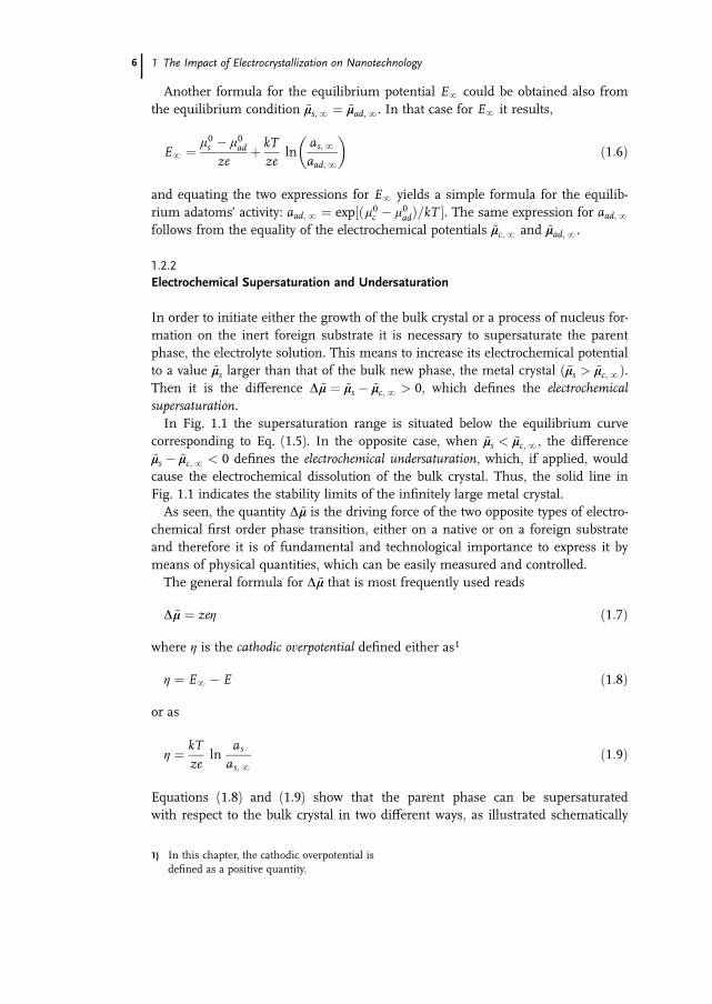
Kinetics of Nucleus Formation in Electrocrystallization
The nucleation work D ~GGðncÞ is a measure of the thermodynamic barrier, which
has to be overcome in order to transform nc ions from the electrolyte solution
into an nc-atomic nucleus of the new solid or liquid phase on the electrode surface.
The rate JðtÞ of this process is a kinetic quantity and here we will comment upon
its overpotential and concentration dependence in the case of a stationary nuclea-
tion when JðtÞ attains the constant value J0.The general theoretical formula for J0 reads [2, 85, 86]
J0 ¼ Z0Wl�1 exp �D ~GGðncÞkT
� �ð1:16Þ
where Z0/cm�2 is the number density of active sites on the substrate, W/s�1 is the
frequency of attachment of single atoms to the critical nucleus and l�1 is a non-
dimensional quantity accounting for the difference between the quasi-equilibrium
and the stationary number of critical nuclei. In the macroscopic classical nuclea-
tion theory l�1 is given as l�1 ¼ ½D ~GGðncÞ=3pn2c kT �
1=2 and is called a ‘‘Zeldovich
factor’’. It tends to unity at high supersaturations and/or very active substrates,
when the critical nuclei are very small and their size remains constant over wide
supersaturation intervals. For this typical case of electrochemical phase formation,
particularly on foreign substrates, we shall reveal the overpotential and the concen-
tration dependence of the stationary nucleation rate in terms of the atomistic
theory of electrochemical phase formation [7, 15, 73, 87]. In this case the quantity
W is given by
W ¼ kn exp � U
kT
� �exp � azeE
kT
� �ð1:17Þ
where kn is a frequency factor, c is the concentration of metal ions, a is the charge
transfer coefficient and U is the energy barrier to transfer of an ion from the elec-
trolyte to the critical nucleus at an electrode potential E ¼ 0. This formula for W is
suitable when the supersaturation D~mm (Eq. (1.7)) is varied by changing the concen-
tration of metal ions at a constant electrode potential E (Fig. 1.1), and substituting
Eqs. (1.7), (1.9), (1.11) and (1.17) into Eq. (1.16) for the J0ðcÞ relationship at
l�1 ! 1 one obtains [7, 68]:
J0 ¼ Z0WðEÞcncþ1 ð1:18Þ
Here
WðEÞ ¼ kng
gycy
� �nc
exp �U þ azeE þ ~FFðncÞkT
� �ð1:19Þ
10 1 The Impact of Electrocrystallization on Nanotechnology

where cy is the equilibrium concentration of metal ions at the temperature T and
g and gy are the corresponding activity coefficients given as g ¼ as=c and
gy ¼ as;y=cy. Thus Eq. (1.18) shows that the size nc of the critical nucleus can
be determined from an experimental J0ðcÞ relationship obtained at E ¼ const ac-cording to [7, 68]:
nc ¼d ln J0d ln c
� 1 ð1:20Þ
In the case when the supersaturation is varied by varying the electrode potential
E at a constant concentration cy ¼ gyas;y (Fig. 1.1) it turns out to be convenient
to introduce the cathodic overpotential h ¼ Ey � E in Eq. (1.17). Then accounting
for the Eyðas;yÞ relationship according to the Nernst equation (1.5) for the over-
potential dependence of the stationary nucleation rate J0 at l�1 ! 1 one obtains
[7, 68]:
J0 ¼ Z0WðcyÞ exp ðnc þ aÞzehkT
� �ð1:21Þ
where
WðcyÞ ¼ knðgycyÞ1�a exp �U þ azeE 0 þ ~FFðncÞkT
" #ð1:22Þ
As seen, in this case the size nc of the critical nucleus can be determined from an
experimental J0ðhÞ relationship obtained at c ¼ cy according to [7, 68]:
nc ¼kT
ze
d ln J0dh
� a ð1:23Þ
Equations (1.16)–(1.23) are derived under the assumption of a constant number
Z0 of active sites on the working electrode, which is a most simple example of elec-
trochemical phase formation. In reality, the number of active sites could be a time,potential and pH dependent quantity [7, 66, 67].
1.4
Energy State of the Electrode Surface and Spatial Distribution of Nanoclusters
The concept of ‘‘active sites’’ unavoidably raises the question about their physical
nature and we should point out that the active sites are probably the most obscure
characteristics of the nucleation kinetics. The reason is that, depending on the spe-
cific properties of the particular electrochemical system, the active sites may be
entirely different nano-objects appearing on or disappearing from the electrode
1.4 Energy State of the Electrode Surface and Spatial Distribution of Nanoclusters 11

surface due to various chemical and/or electrochemical reactions taking place
prior to or simultaneously with the process of nucleus formation. These could be
adsorption and desorption of organic and inorganic ions or molecules, surface
transformations within preformed UPD layers, direct oxidation or reduction of
the electrode surface etc. All this means that the assumption of an ‘‘inert’’ working
electrode is certainly a serious approximation and a theoretical model of nucleus
formation on a time-dependent number of active sites is developed in Refs. [7, 66,
67]. Without entering into detail we shall point out that if active sites appear on
and disappear from the electrode surface as a result of an electrochemical reaction,
parallel to the process of nucleus formation, the time dependence of the number
NðtÞ of nuclei may be expressed by means of the following second-order differen-
tial equation [7, 66, 67]:
d2N
dt2þ A
dN
dtþ BðN � N0Þ ¼ 0 ð1:24Þ
Here A and B depend on the nucleation frequency Kn ¼ Wl�1 exp½�D ~GGðncÞ=kT �and on the frequencies of appearance Kþ
a and disappearance K�a of active sites to
and from the electrode surface. N0 ¼ Z0a þ Z0
l is the total number of active sites at
time t ¼ 0, Z0a and Z0
l being the numbers of the available and of the latent active
sites at the time moment t ¼ 0.
Exact analytical solution of Eq. (1.24) is possible and yields theoretical expres-
sions for the nucleation rate JðtÞ ¼ dNðtÞ=dt and for the number of nuclei NðtÞin the case of a time-dependent number of active sites. Figure 1.4 illustrates the
obtained result and shows that the nucleation rate has a non-zero initial value
Figure 1.4. Non-dimensional plots JðxÞ=Jð0Þ (1) and NðxÞ=N0 (2)
versus x ¼ t=tm calculated according to the theoretical model of
nucleus formation on a time-dependent number of active sites
[7, 66, 67].
12 1 The Impact of Electrocrystallization on Nanotechnology

Jð0Þ ¼ ðdN=dtÞt¼0 ¼ KnZ0a , a zero final value, JðyÞ ¼ 0, and displays a maximum,
at time t ¼ tm. As for NðtÞ it changes from zero to the maximal value
N0 ¼ Z0a þ Z0
l at sufficiently long times when all latent active sites are developed
and occupied by the nuclei of the new phase.
The detailed theoretical analysis carried out in Refs. [7, 66, 67] shows that, in
this complex case of electrochemical phase formation, a stationary state may be es-
tablished only under special circumstances and after a certain induction period. It
turns out, also, that the quantity which we use to measure and to call a stationarynucleation rate may provide experimental information not on the nucleation kinetics
but on the kinetics of appearance of active sites on the electrode surface, if this pro-
cess is the rate determining step in the initial stage of the phase transition. This
finding must be taken into consideration when interpreting experimental data on
the kinetics of nucleus formation, both on foreign and on native substrates.
An important question closely related to the nucleation kinetics concerns the lo-
cation of nuclei on the electrode surface. In particular, it turns out to be important
for many practical purposes to know whether nanoclusters are randomly distrib-
uted on the substrate or whether there is a certain cluster–cluster correlation. Themost frequently used approach to this problem consists in the statistical analysis
of the distances between nearest neighbor clusters and comparison of the obtained
results with theoretical formulae based on the Poisson law for a purely random dis-
tribution [88, 89]. Here we present some experimental data interpreted by means
of the general theoretical expression for the probability distribution function
dPn;n of the distances between nth neighbor clusters randomly located within a
n-dimensional space, derived in Ref. [90]:
dPn;n ¼ n
ðn� 1Þ!pn=2N0; n
Gð1þ n=2Þ
" #n
r nn�1n;n exp �
pn=2N0; nr nn;nGð1þ n=2Þ
" #drn;n ð1:25Þ
In fact Eq. (1.25) gives us the probability dPn;n for a given cluster to have its nthneighbor at a distance between rn;n and rn;n þ drn;n and in it N0; n is the average
cluster density, G is the gamma function and n is the space dimension. Thus
n ¼ 1 if clusters are formed on a step, n ¼ 2 if clusters are formed on a surface
and n ¼ 3 if clusters are incorporated within a three-dimensional matrix, e.g. with-
in the bulk of an electrically conducting medium. Correspondingly, the average dis-
tance rn;n between clusters is defined as
rn;n ¼ðy0
rn;n dPn;nGðnþ 1=nÞðn� 1Þ!
ðGðnþ n=2Þpn=2N0; n
� �1=n
ð1:26Þ
Figure 1.5 illustrates the correlation between the experimental (histograms) and
theoretical (lines) distributions of the distances between first, second and third
neighbor silver crystals electrodeposited on a mechanically polished glassy carbon
electrode [91]. As seen, in all cases the experimentally measured smallest distances
appear with a probability lower than theoretically predicted for a random distribu-
1.4 Energy State of the Electrode Surface and Spatial Distribution of Nanoclusters 13

tion, the effect being less pronounced for second and for third neighbor clusters.
This should mean that zones of reduced nucleation rate arise around the growing
stable clusters, of course, if we assume that the active sites themselves are ran-
domly distributed on the electrode surface. This has been proven to be the case
for the mechanically polished glassy carbon working electrode [91]. However, it
might not necessarily be true for other amorphous or crystalline substrates.
Deviations from the random distribution were experimentally registered also in
other electrochemical systems [76, 79, 92–95] and were also confirmed by means
of computer simulations [96, 97]. In the next section we consider the electrochem-
ical growth of nanoclusters and comment upon the physical nature of the zones of
reduced nucleation rate.
1.5
Electrochemical Growth of Nanoparticles and Ultrathin Films
The growth kinetics of three- and two-dimensional (3D and 2D) clusters have been
examined by many authors and under different experimental conditions account-
Figure 1.5. Experimental (histograms) and theoretical (lines)
distribution of the distances between first (a), second (b) and third (c)
neighbor silver crystals electrochemically deposited on a flat glassy
carbon electrode, N0; 2 ¼ 2:75� 104 cm�2 [91].
14 1 The Impact of Electrocrystallization on Nanotechnology

ing for various limitation factors (see e.g. Refs. [3–8] and the literature cited there-
in). Here we present briefly only the basic theoretical and experimental findings.
1.5.1
Growth of 3D Nanoclusters
At a constant overpotential h the current I1ðtÞ of a single hemispherical cluster
growing under the conditions of combined charge transfer and diffusion limita-
tions is given by [98]:
I1ðtÞ ¼ p1þ nt
ð1þ 2ntÞ1=2� 1
" #ð1:27Þ
In Eq. (1.27)
p ¼ 4pðzFDcyÞ2
i0exp � azFh
RT
� �� exp �ð1þ aÞzFh
RT
� �� �ð1:28Þ
n ¼ VMi20ðzFÞ2Dcy
exp2azFh
RT
� �� exp �ð1� 2aÞzFh
RT
� �� �ð1:29Þ
where D is the diffusion coefficient of metal ions and i0 is the exchange current
density at the cluster–solution interface boundary.
The growth of a single cluster affects significantly both the concentration and the
overpotential distribution in the cluster vicinity [96, 99, 100]. Thus the concentra-
tion cðrÞ and the overpotential hðrÞ at a distance r from the cluster are given by:
cðrÞ ¼ cy 1� I1ðtÞ2przFDcy
� �ð1:30Þ
hðrÞ ¼ hþ RT
zFln 1� I1ðtÞ
2przFDcy
� �ð1:31Þ
and substituting these two formulae into Eq. (1.21), for the stationary nucleation
rate J0ðrÞ at a distance r one obtains
J0ðrÞ ¼ J0 1� I1ðtÞ2przFDcy
� �ncþ1
ð1:32Þ
The solid line in Fig. 1.6 illustrates the non-dimensional distribution of the station-
ary nucleation rate around a growing hemispherical cluster, if the single atom ad-
sorbed on the electrode surface is a critical nucleus ðnc ¼ 1Þ within the entire zone
of reduced concentration and overpotential. However, since the critical nucleus
size is a function of the overpotential hðrÞ it appears that, in the general case, dif-
ferent clusters may play the role of critical nuclei in the vicinity of the growing
1.5 Electrochemical Growth of Nanoparticles and Ultrathin Films 15

supercritical one and this yields much more complex distribution of the nucleation
rate [7, 101].
If multiple hemispherical clusters form and grow on the electrode surface then
the local zones of reduced nucleation rate spread out and gradually overlap, which
means that a general theoretical model describing the overall nucleation kinetics
should account for the collective interaction between a large number of growing
clusters. The problem has no exact solution and a most frequently employed
approximation is based on the idea of overlapping planar diffusion zones in which
nucleation is fully arrested [14, 102–106] (Fig. 1.6). Thus, in the case of growth of
clusters under the conditions of complete diffusion control, for the total current
one obtains:
iNðtÞ ¼ bzFcD
pt
� �1=21� exp � 1
2J0pð8pcVMÞ1=2Dt2
� �� �ð1:33Þ
if NðtÞ clusters are progressively formed on the electrode surface during the time in-
terval ð0; tÞ and
iN0ðtÞ ¼ zFc
D
pt
� �1=2f1� exp½�N0pð8pcVMÞ1=2Dt�g ð1:34Þ
if N0 clusters appear instantaneously at the initial moment t ¼ 0. In Eq. (1.33) b is a
numerical constant, which equals 1 according to Refs. [14, 102] and 4/3 according
to Refs. [105, 106].
Figure 1.6. Cross section of a non-dimensional distribution of the
stationary nucleation rate around a spherical cluster for the case nc ¼ 1
atom (——). Profile of a planar nucleation exclusion zone (----).
16 1 The Impact of Electrocrystallization on Nanotechnology

A specific feature of electrochemical nucleation is the existence of an overpoten-
tial threshold (‘‘critical overpotential’’ hcrit) below which the nucleation rate J0 is
practically zero and above which it raises exponentially (cf. Eq. (1.16)) [1–8]. Based
on this feature an efficient double-pulse polarization routine for metal electrodepo-
sition was developed, as illustrated schematically in Fig. 1.7 (see e.g. Refs. [5, 7]
and the references cited therein).
The double-pulse technique allows the formation, either progressively or instanta-neously, of a large number of metal clusters during the first short pulse at h1 g hcrit.
This pulse is followed by a second one of a much lower cathodic overpotential
h2 f hcrit during which only further growth of clusters is possible. This polarization
routine has been successfully applied both for electrodeposition of metal nanopar-
ticles with a narrow size distribution [107, 108] and for electroplating of compact
thin metal films [20, 109, 110].
1.5.2
Growth of 2D Nanoclusters and Formation of UPD Monolayers
As already mentioned in Section 1.2.2, in systems characterized by strong interac-
tion energy between the depositing metal and the foreign substrate the deposition
of the bulk metal phase can be preceded by UPD of different low-dimensional
metal or alloy phases [5, 11, 51–65, 111–121]. In such systems, at potentials close
to the equilibrium potential Ey, the foreign substrate is usually covered by con-
densed UPD monolayers, which can be either commensurate or incommensurate,
depending on the crystallographic deposit–substrate misfit.
Figures 1.8 and 1.9 illustrate the evolution of surface morphology during the
UPD of condensed Ag and Pb monolayers on stepped Au(100) and Ag(111) sub-
strates, respectively [5, 56, 63, 111, 114–117, 120]. As seen in Fig. 1.8, the con-
Figure 1.7. Schematic representation of the double-pulse polarization
routine for preparation of metal nanoparticles and compact metal
films.
1.5 Electrochemical Growth of Nanoparticles and Ultrathin Films 17

densed Ag monolayer on Au(100) is formed by multiple nucleation and growth of
2D Ag clusters occurring simultaneously at monatomic steps and on flat terraces
[116, 117]. The STM imaging with atomic resolution shows that the condensed
Ag monolayer is commensurate, as expected because of the very low AgaAu misfit.
In contrast to this, a compressed close-packed incommensurate Pb monolayer is
Figure 1.8. UPD of Ag on a stepped Au(100) substrate. Electrolyte: 5
mM Ag2SO4 þ 0.1 M H2SO4 (T ¼ 298 K). (a) in situ STM image of the
substrate surface at underpotential E � Ey ¼ 400 mV. (b) in situ STM
image showing the formation of a condensed Ag monolayer at
underpotential E � Ey ¼ 15 mV.
Figure 1.9. UPD of Pb on a stepped Ag(111) substrate. Electrolyte:
5 mM Pb(ClO4)2 þ 0:5 M Na(ClO4)2 þ 5 mM HClO4 (T ¼ 298 K).
(a) in situ AFM image showing the 1D and 2D Pb phase formation
(b) applied polarization routine.
18 1 The Impact of Electrocrystallization on Nanotechnology

formed on Ag(111) due to the significant PbaAg misfit [5, 56, 63, 111, 115, 116,
120]. Figure 1.9 shows that in this case the formation of the condensed Pb mono-
layer (2D Pb phase) starts exclusively at substrate monatomic steps. The linescan
ðx � tÞ AFM image indicates also that the monolayer growth is preceded by a dec-
oration of the monatomic steps and formation of a ‘‘1D Pb phase’’ occurring at po-
tentials more positive than the equilibrium potential E2D of the condensed 2D Pb
phase. These observations clearly show that substrate monatomic steps play an im-
portant role in the formation of condensed UPD monolayers and have to be taken
into account in the theoretical models describing the kinetics of 2D nucleation and
growth [56].
As a surface limited process, UPD offers attractive possibilities for surface mod-
ification on an atomic scale and preparation of nanomaterials with unconventional
chemical and physical properties. Some important examples are summarized sche-
matically in Fig. 1.10. Underpotential codeposition from multicomponent electro-
lytes is used successfully in the so-called ‘‘electrochemical atomic layer epitaxy’’
(EC-ALE) for a nanoscale controlled preparation of different superlattices and ultra-
thin films of metals, alloys and semiconducting compounds, as illustrated sche-
matically in Fig. 1.10(a) and (b) [5, 51, 61, 122–124]. Another interesting appli-
cation of the UPD phenomena is to use an UPD metal layer as a surfactant
influencing the kinetics and mechanism of electrochemical growth of a more
noble metal [125–128]. In this case, the UPD metal layer floats on the surface of
the growing noble metal (Fig. 1.10(c)) and the growth process involves a place-
exchange between the depositing metal atoms and the atoms of the UPD layer. It
Figure 1.10. Possible applications of UPD in nanotechnology (a
schematic representation). (a) deposition of superlattices and
multilayers, (b) deposition of ultrathin alloy and compound films,
(c) electrochemical surfactant mediated growth, (d) monolayer
modification of nanoparticles.
1.5 Electrochemical Growth of Nanoparticles and Ultrathin Films 19
was demonstrated that the use of Pb as a surfactant in the electrochemical deposi-
tion of Ag on Ag(111) and Au(111) facilitates a layer-by-layer growth mode [125,
126]. Recently Pb and Tl were used successfully as surfactants enhancing the elec-
trodeposition rate of Au in order to achieve a ‘‘superfill’’ (perfect filling) of nano-
sized trenches according to the so-called ‘‘curvature enhanced accelerator coverage’’
(CEAC) mechanism [127, 128]. As illustrated in Fig. 1.10(d), the UPD process can
be applied also for surface modification of metal nanoparticles by a monolayer of a
second metal [129–131]. The use of substrates such as graphite or glassy carbon,
which are inert with respect to metal UPD, is suitable in this case. Noble metal
nanoparticles with a controlled size can be electrodeposited on the inert substrate
and selectively modified by a subsequent UPD of a less noble metal [131]. Recently
such UPD modification was used as an intermediate step in a new technique for
preparation of novel electrocatalysts based on Pt monolayers deposited on the sur-
faces of carbon-supported non-noble metal/noble metal (core/shell) nanoparticles
(Ni/Au, Co/Pd and Co/Pt) [132]. In this technique the Pt monolayer is deposited
by galvanic displacement of a pre-deposited Cu UPD monolayer. The Pt monolayer
electrocatalysts prepared by this technique are characterized by a mass activity
higher than that of the commercial Pt-containing catalytic materials [132].
1.6
Localization of Electrocrystallization Processes and Nanostructuring
An important property of electrocrystallization is its high selectivity. This property
offers numerous possibilities for localization of electrocrystallization processes and
preparation of nanostructures for fundamental research and technological applica-
tions. A widely applied method for localized electrocrystallization is based on the
use of insulating templates such as lithographically patterned resist layers or nano-
porous membranes (see e.g. Refs. [133, 134], Chapter 3 in this book and the refer-
ences cited therein). The modification of a conducting substrate with an insulating
template results in the formation of negative (recessed) structures. A single nega-
tive structure of this type is shown schematically in Fig. 1.11. For the filling of such
a structure by electrodeposition, its aspect ratio h=d (depth/diameter) and the sur-
face state of the conducting substrate are important. As already discussed in Sec-
tion 1.4, the energy state of the substrate surface determines the density of active
nucleation sites Z0 and the nucleation rate J0. The initial stages of localized electro-
crystallization in the negative structure can be characterized by the mean nuclea-
tion time tn ¼1
J0pðd=2Þ2and the mean time tL ¼
d
VLneeded for the first cluster to
cover the bottom surface of the structure. Here pðd=2Þ2 and VL represent the bot-
tom area of the structure and the lateral growth rate of the crystalline cluster, re-
spectively. Two different growth modes can generally be distinguished, depending
on the electrocrystallization conditions, as illustrated schematically in Fig. 1.11: (i)
a mononuclear growth mode occurring at tn g tg through the formation and growth
20 1 The Impact of Electrocrystallization on Nanotechnology

of a single nucleus and (ii) a multinuclear growth mode occurring at tn f tg through
the formation and growth of a large number of crystalline nuclei. The localized
electrocrystallization by the mono- or multinuclear growth mode can be applied
successfully for the fabrication of single- or polycrystalline metal nanowires with
extremely high aspect ratios, as demonstrated recently using nanoporous polymer
membranes as templates [135, 136]. Another approach to the preparation of vari-
ous metal and compound nanowires is based on the preferred electrocrystallization
at step edges (see e.g. Refs. [108, 137–139] and Chapter 9 in this book).
The invention of scanning probe microscopy (SPM) opened a new window not
only for in situ surface studies of electrode surfaces at an atomic scale but also for
the local nanostructuring and modification of surfaces by electrochemical phase
formation using the SPM tip as a nanoelectrode (cf. Fig. 1.12(a)). In this case the
ratio between the polarization resistance Rpol (including the resistances for the
charge transfer through the new formed phase and interfaces) and the electrolyte
resistance Rel in the electrochemical in situ SPM cell [140–142] is crucial for the
localization. Electrochemical phase formation can be localized if Rpol fRel (cf.
Fig. 1.12(b)). Such localized electrocrystallization was successfully realized by
means of in situ STM in the case of metal electrodeposition from dilute electrolyte
solutions (see e.g. Refs. [56, 63, 69–72] and Chapter 6 in this book). For Rpol gRel,
however, the formation of the new phase in the electrochemical in situ SPM cell
becomes fully delocalized. Thus, no localized formation of insulating anodic oxides
could be achieved by in situ SPM, even in pure water, due to the very high resis-
tance of the oxide phases ðRpol gRelÞ. In this case the localization of the oxidation
process can be realized by ex situ SPM in a humid atmosphere. Under these con-
ditions the water vapors condense between the SPM tip and the substrate forming
a water meniscus, which acts as electrolyte and localizes the electrochemical oxida-
tion (Fig. 1.13a). This approach is widely used for preparation of various nanostruc-
Figure 1.11. Mono- and multinuclear growth modes in a negative
insulator/conductor structure (a schematic representation).
1.6 Localization of Electrocrystallization Processes and Nanostructuring 21

tures by local AFM tip-induced anodic oxidation of semiconductors and valve met-
als [23, 46, 140–148]. Figure 1.13(b) shows, as an example, a pattern composed of
linear oxide structures fabricated by scanning a conducting AFM tip on a p-Si sub-
strate in humid air [142]. The height and the width of the oxide structures depend
on the applied bias voltage DU, the scan rate of the AFM tip and the relative
humidity of the atmosphere. Figures 1.14(a) and (b) show the voltage dependence
Figure 1.12. (a) Schematic representation of localized electrodeposition
in the in situ SPM cell. (b) Schematic log Rpol � log Rel plot showing
the localization conditions.
Figure 1.13. Localized anodic oxidation induced by the AFM tip. (a)
Schematic representation of the electrochemical nanocell formed
between the AFM tip and the substrate in humid atmosphere. (b) SiO2
pattern fabricated by local AFM tip-induced oxidation of p-Si(111) (bias
voltage DU ¼ 8:5 V, tip scan rate 200 nm s�1, relative humidity 3%).
22 1 The Impact of Electrocrystallization on Nanotechnology

of Nb2O5 dots generated by localized anodic oxidation of a thin Nb film at fixed
AFM tip position (point oxidation) and constant polarization time. The anodic
oxidation of Nb is a substrate-consuming electrode reaction (2Nbþ 5H2O !Nb2O5 þ 10Hþ þ 10e�), in which two moles Nb are needed for the formation of
one mole Nb2O5. Thus, the increase in the thickness Ddox of the generated oxide
dots can be estimated from their height hox (cf. Fig. 1.14(b)) using the relation
Ddox ¼ 1:56hox where the factor 1.56 is determined by the molar volumes of Nb
and Nb2O5 [140]. The derived linear Ddox � DU dependence shown in Fig. 1.14(c)
is in good agreement with the high-field law of the oxide growth [23, 45].
The preparation of lateral metal–insulator–metal (MIM) structures by local oxi-
dation is of particular interest for nanoelectronics. Thus it is essential to find opti-
mal conditions for a complete AFM tip-induced local oxidation of a thin metal film.
Figure 1.15 shows an experimental routine, which has been used to control the
complete local oxidation of a 5 nm thick Nb film sputtered on a thermally-oxidized
silicon substrate [140]. Square structures were first fabricated with a scan rate of
the AFM tip of 200 nm s�1 and bias voltages DU ranging between 6 and 12 V
(Fig. 1.15(a)). In a second step, an attempt was made for a local oxidation of Nb
along a 500 nm line inside each square structure in order to check if there is still
an electric contact between Nb film inside and outside each square structure (Fig.
1.15(b)). The results obtained show that under the given experimental conditions a
complete oxidation of the thin Nb film can be achieved at bias voltages higher than
10 V. The generated structures are presented schematically in Fig. 1.15(c). This
approach can be applied successfully for the fabrication of different lateral MIM
structures by local AFM tip-induced nanooxidation of ultrathin films of valve
metals.
Figure 1.14. (a) Nb2O5 dots generated on a 20 nm thick Nb film by a
fixed AFM tip applying different bias voltages DU (polarization time
tp ¼ 10 s, relative humidity 40%). (b) Single line section of the AFM
image in (a). (c) Ddox � DU dependence derived from (b).
1.6 Localization of Electrocrystallization Processes and Nanostructuring 23

1.7
Conclusion
In this chapter we discuss some selected aspects of electrocrystallization, which are
relevant for a better understanding of both the nucleation and growth phenomena
at an atomic level and the preparation of various nanostructures by electrochemical
means. The presented examples demonstrate in how many respects the concepts
of electrocrystallization affect the future development of nanotechnology. In partic-
ular this applies to the preparation of nanoparticles by controlled nucleation and
growth, to the formation of atomic scale thin films and superlattices by underpo-
tential deposition, to the fabrication of single- and polycrystalline nanowires by
template electrodeposition and selective electrocrystallization at step edges and to
the nanostructuring of metal and semiconductor substrates by SPM tip-induced
electrocrystallization of metals and oxides.
Figure 1.15. Experimental routine used for checking the complete local
oxidation of a Nb thin film (Nb film thickness 5 nm, AFM tip scan rate
200 nm s�1, relative humidity 40%). (a) Nb2O5 structures prepared by
tip-induced oxidation with different bias voltages. (b) AFM image
obtained after an attempt for tip-induced oxidation with DU ¼ 10 V
inside the square structures in (a). (c) Schematic representation of the
structures in (b).
24 1 The Impact of Electrocrystallization on Nanotechnology

Acknowledgments
The authors gratefully acknowledge the financial support given by the Research
Centre Julich, the Bulgarian Academy of Sciences and the German Research Asso-
ciation (DFG).
References
1 M. Volmer, Das elektrolytischeKristallwachstum, Hermann et Cie,
Paris, 1934.
2 M. Volmer, Kinetik der Phasenbildung,Steinkopf, Dresden, 1939.
3 H. Fischer, Elektrolytische Abscheidungund Elektrokristallisation von Metallen,Springer, Berlin, 1954.
4 J. O’M. Bockris, G. A. Razumney,
Fundamental Aspects of Electrocrys-tallization, Plenum Press, New York,
1967.
5 E. Budevski, G. Staikov, W. J.
Lorenz, Electrochemical PhaseFormation and Growth – An Introduc-tion to the Initial Stages of MetalDeposition, VCH, Weinheim, 1996.
6 M. Paunovic, M. Schlesinger,
Fundamentals of ElectrochemicalDeposition, Wiley-Interscience, New
York, 1998.
7 A. Milchev, Electrocrystallization:Fundamentals of Nucleation andGrowth, Kluwer Academic Publishers,
Boston/Dordrecht/London, 2002.
8 M. Fleischmann, H. R. Thirsk, in
Advances in Electrochemistry andElectrochemical Engineering, Vol. 3,P. Delahay (Ed.), Wiley, New York,
1963.
9 H. Fischer, Angew. Chem. Int. Ed.Engl. 1969, 8, 108.
10 J. O’M. Bockris, A. R. Despic, in
Physical Chemistry – An AdvancedTreatise, Vol. IXB, H. Eyring, D.
Henderson, W. Jost (Eds.), Academic
Press, New York, 1970.
11 D. M. Kolb, in Advances inElectrochemistry and ElectrochemicalEngineering, Vol. 11, H. Gerischer,
C. W. Tobias (Eds.), Wiley, New York,
1978.
12 E. Budevski, V. Bostanov,
G. Staikov, Annu. Rev. Mater. Sci.1980, 10, 85.
13 E. Budevski, in Comprehensive Treatiseof Electrochemistry, Vol. 7, B. E.Conway, J. O’M. Bockris, E. Yeager,
S. U. M. Kahn, R. E. White (Eds.),
Plenum Press, New York, 1983.
14 B. Scharifker, G. Hills, Electrochim.Acta 1983, 28, 879.
15 A. Milchev, Contemp. Phys. 1991, 32,321.
16 P. Allongue, in Modern Aspects ofElectrochemistry, Vol. 23, B. E. Conway,J. O’M. Bockris, R. E. White (Eds.),
Plenum Press, New York, 1992.
17 E. Michailova, I. Vitanova,
D. Stoychev, A. Milchev,
Electrochim. Acta 1993, 38, 2455.18 A. I. Danilov, E. B. Molodkina,
Yu. M. Polukarov, Russ. J.Electrochem. 1994, 30, 674.
19 M. H. Holzle, V. Zwing, D. M. Kolb,
Electrochim. Acta 1995, 40, 1237.20 G. Oskam, J. G. Long, A. Natarajan,
P. C. Searson, J. Phys. D: Appl. Phys.1998, 31, 1927.
21 E. Budevski, G. Staikov, W. J. Lorenz,
Electrochim. Acta 2000, 45, 2499.22 R. Krumm, B. Guel, C. Schmitz,
G. Staikov, Electrochim. Acta 2000, 45,3255.
23 G. Staikov, in ElectrochemicalMicrosystem Technologies, J. W.
Schultze, T. Osaka, M. Datta (Eds.),
Taylor & Francis, London and New
York, 2002.
24 K. Marquez, G. Staikov, J. W.
Schultze, Electrochim. Acta 2003, 48,875.
25 A. Milchev, T. Zapryanova,
Electrochim. Acta 2006, 51, 2926.
References 25
26 P. C. Andricacos, C. Uzoh, J. O.
Dukovic, J. Horkans, H. Deligianni,
IBM J. Res. Develop. 1998, 42, 567.27 P. C. Andricacos, Interface 1999, 8,
32.
28 A. Brenner, Electrodeposition of Alloys,Academic Press, New York, 1963.
29 K. M. Gorbunova, Yu. M.
Polukarov, in Advances inElectrochemistry and ElectrochemicalEngineering, Vol. 5, P. Delahay (Ed.),Wiley, New York, 1967.
30 F. A. Kroger, J. Electrochem. Soc.1978, 125, 2028.
31 P. C. Andricacos, C. Arana, J. Tabib,
J. Dukovic, L. T. Romankiw,
J. Electrochem. Soc. 1989, 136, 1336.32 A. Milchev, R. Lacmann, J. Cryst.
Growth 1991, 110, 919, 925.33 K. Rajeshwar, Adv. Mater. 1992, 4, 23.34 D. Landolt, Electrochim. Acta 1994,
39, 1075.35 G. Hodes, in Physical Electrochemistry,
I. Rubinstein (Ed.), Marcel Dekker,
New York, 1995.
36 E. Michailova, A. Milchev, R.
Lacmann, Electrochim. Acta 1996, 41,329.
37 A. Milchev, Electrochim. Acta 1997,
42, 1533.38 A. Milchev, E. Michailova,
T. Zapryanova, Electrochem. Commun.2004, 6, 713.
39 A. Milchev, G. Staikov, Indian J.Chem. 2005, 44A, 899.
40 L. Young, Anodic Oxide Films,Academic Press, London, 1961.
41 D. A. Vermilyea, in Advances inElectrochemistry and ElectrochemicalEngineering, Vol. 3, P. Delahay (Ed.),Wiley, New York, 1963.
42 M. J. Dignam, in ComprehensiveTreatise of Electrochemistry, Vol. 4,J. O’M. Bockris, B. E. Conway,
E. Yeager, R. E. White (Eds.),
Plenum Press, New York, 1981.
43 M. Fleischmann, L. J. Li, L. M.
Peter, Electrochim. Acta 1989, 34,475.
44 B. E. Conway, B. Barnett,
H. Angerstein-Kozlowska, B. V.
Tilak, J. Chem. Phys. 1990, 93, 8361.45 J. W. Schultze, M. M. Lohrengel,
Electrochim. Acta 2000, 45, 2499.
46 H. Bloeß, G. Staikov, J. W.
Schultze, Electrochim. Acta 2001, 47,335.
47 V. Lehmann, Electrochemistry ofSilicon: Instrumentation, Science,Materials and Applications, Wiley-VCH,
Weinheim, 2002.
48 G. Binnig, H. Rohrer, Helv. Phys.Acta 1982, 55, 726.
49 P. Lustenberger, H. Rohrer,
R. Christoph, H. Siegenthaler,
J. Electroanal. Chem. 1988, 243, 225.50 H. Siegenthaler, in Scanning
Tunneling Microscopy II, Springer Ser.Surf. Sci., Vol. 28, R. Wiesendanger,
H.-J. Guntherodt (Eds.), Springer,
Berlin, 1992.
51 G. Staikov, K. Juttner, W. J.
Lorenz, E. Budevski, Electrochim.Acta 1994, 39, 1019.
52 A. A. Gewirth, H. Siegenthaler
(Eds.), Nanoscale Probes of the Solid/Liquid Interface, Kluwer Academic
Publishers, Dordrecht/Boston/London,
1995.
53 P. Allongue, in Advances inElectrochemical Science and Engineering,Vol. 4, H. Gerischer, C. W. Tobias
(Eds.), VCH, Weinheim, 1995.
54 W. Plieth, W. J. Lorenz (Eds.),
Electrochemical Nanotechnology, Wiley-
VCH, Weinheim, 1998.
55 K. Itaya, Prog. Surf. Sci. 1998, 58,121.
56 G. Staikov, W. J. Lorenz, E.
Budevski, in Imaging of Surfaces andInterfaces (Frontiers in Electrochemistry,Vol. 5), J. Lipkowski, P. N. Ross
(Eds.), Wiley-VCH, New York, 1999.
57 R. J. Nichols, in Imaging of Surfacesand Interfaces (Frontiers in Electro-chemistry, Vol. 5), P. N. Ross, J.Lipkowski (Eds.), Wiley-VCH, New
York, 1999.
58 T. P. Moffat, in ElectroanalyticalChemistry, Vol. 21, A. J. Bard,I. Rubinstein (Eds.), Marcel Dekker,
New York, 1999.
59 D. M. Kolb, Electrochim. Acta 2000,
45, 2387.60 D. M. Kolb, in Advances in Electro-
chemical Science and Engineering,Vol. 7, R. C. Alkire, D. M. Kolb
(Eds.), Wiley-VCH, Weinheim, 2001.
26 1 The Impact of Electrocrystallization on Nanotechnology

61 J. L. Stickney, in Advances inElectrochemical Science and Engineering,Vol. 7, R. C. Alkire, D. M. Kolb
(Eds.), Wiley-VCH, Weinheim, 2001.
62 D. P. Barkey, in Advances in Electro-chemical Science and Engineering, Vol.7, R. C. Alkire, D. M. Kolb (Eds.),
Wiley-VCH, Weinheim, 2001.
63 W. J. Lorenz, G. Staikov,
W. Schindler, W. Wiesbeck,
J. Electrochem. Soc. 2002, 149, K47.64 W. Polewska, R. J. Behm, O. M.
Magnussen, Electrochim. Acta 2003,
48, 2915.65 W. Freyland, C. A. Zell, S. Zein El
Abedin, F. Endres, Electrochim. Acta2003, 48, 3053.
66 A. Milchev, J. Electroanal. Chem.,1998, 457, 35.
67 A. Milchev, J. Electroanal. Chem.,1998, 457, 47.
68 A. Milchev, E. Michailova,
Electrochem. Commun., 2000, 2, 15.69 R. T. Potzschke, G. Staikov, W. J.
Lorenz, W. Wiesbeck, J. Electrochem.Soc., 1999, 146, 141.
70 W. Schindler, D. Hofmann,
J. Kirschner, J. Electrochem. Soc.,2001, 148, C124.
71 W. Schindler, P. Hugelmann,
M. Hugelmann, F. X. Kartner,
J. Electroanal. Chem., 2002, 522, 49.72 R. Widmer, H. Siegenthaler,
Electrochem. Commun., 2005, 7, 421.73 A. Milchev, S. Stoyanov,
J. Electroanal. Chem., 1976, 72, 33.74 S. Stoyanov, in Current Topics in
Materials Science, Vol. 3, E. Kaldis(Ed.), North-Holland, Amsterdam,
1978.
75 J. Mostany, J. Parra, B. R.
Scharifker, J. Appl. Electrochem.,
1986, 16, 333.76 A. Serruya, B. R. Scharifker,
I. Gonzalez, M. T. Oropeza,
M. Palomar-Pardave, J. Appl.Electrochem., 1996, 26, 451.
77 M. Palomar-Pardave, Ma. Teresa
Ramirez, I. Gonzalez, A. Serruya,
B. R. Scharifker, J. Electrochem. Soc.,1996, 143, 1551.
78 A. Kelaidopoulou, G. Kokkinidis,
A. Milchev, J. Electroanal. Chem.
1998, 444, 195.
79 A. Serruya, J. Mostany, B. R.
Scharifker, J. Electroanal. Chem.,
1999, 464, 39.80 A. Milchev, D. Stoychev, V. Lazarov,
A. Papoutsis, G. Kokkinidis, J. Cryst.Growth, 2001, 226, 138.
81 M. Arbib, B. Zhang, V. Lazarov,
D. Stoychev, A. Milchev, C. Buess-
Herman, J. Electroanal. Chem., 2001,
510, 67.82 L. H. Mendoza-Huizar, J. Robles,
M. Palomar-Pardave, J. Electroanal.Chem., 2002, 521, 95.
83 L. H. Mendoza-Huizar, J. Robles,
M. Palomar-Pardave, J. Electroanal.Chem., 2003, 545, 39.
84 L. H. Mendoza-Huizar, J. Robles,
M. Palomar-Pardave, J. Electrochem.Soc., 2005, 152, 95.
85 R. Becker, W. Doring, Ann. Phys.,1935, 24, 719.
86 Ya. B. Zeldovich, Acta Physicochim,
USSR, 1943, 18, 1.87 A. Milchev, S. Stoyanov, R.
Kaischew, Thin Solid Films, 1974, 22,255, 267.
88 P. Hertz, Math. Ann., 1909, 67, 387.89 S. Chandrasekhar, Rev. Mod. Phys.,
1943, 15, 1.90 A. Milchev, J. Chem. Phys., 1994, 100,
5160.
91 A. Milchev, E. Michailova,
I. Lesigiraska, Electrochem. Commun.,2000, 2, 407.
92 W. S. Kruijt, M. Sluyters-Rehbach,
J. H. Sluyters, A. Milchev,
J. Electroanal. Chem., 1994, 371, 13.93 J. Mostany, A. Serruya, B. R.
Scharifker, J. Electroanal. Chem.,
1995, 383, 33.94 U. Schmidt, M. Donten, J. G.
Osteryoung, J. Electrochem. Soc.,1997, 144, 2013.
95 S. Ivanov, V. Tsakova, J. Appl.Electrochem., 2002, 32, 709.
96 A. Milchev, W. S. Kruijt, M.
Sluyters-Rehbach, J. H. Sluyters,
J. Electroanal. Chem., 1993, 362, 21.97 V. Tsakova, A. Milchev, J. Electroanal.
Chem., 1998, 451, 211.98 S. Fletcher, J. Cryst. Growth, 1983,
62, 505.99 A. Milchev, J. Appl. Electrochem.,
1990, 20, 307.
References 27

100 A. Milchev, J. Electroanal. Chem.,
1991, 312, 267.101 A. Milchev, L. Heerman, Electrochim.
Acta, 2003, 48, 2903.102 G. Gunawardena, G. Hills,
I. Montenegro, B. Scharifker,
J. Electroanal. Chem., 1982, 138, 225.103 B. R. Scharifker, J. Mostany,
J. Electroanal. Chem., 1984, 177, 13.104 M. V. Mirkin, A. P. Nilov,
J. Electroanal. Chem, 1990, 283, 35.105 L. Heerman, A. Tarallo, J. Electroanal.
Chem, 1999, 470, 70.106 L. Heerman, E. Matthijs,
S. Langerock, Electrochim. Acta, 2000,47, 905.
107 H. Liu, F. Favier, K. Ng, M. P. Zach,
R. M. Penner, Electrochim. Acta, 2001,47, 671.
108 R. M. Penner, J. Phys. Chem. B, 2002,106, 3339.
109 K. Marquez, G. Staikov, J. W.
Schultze, Trans. IMF, 2002, 80, 73.110 K. Marquez, R. Ortiz, J. W.
Schultze, O. P. Marquez,
J. Marquez, G. Staikov, Electrochim.Acta, 2003, 48, 711.
111 D. Carnal, P. I. Oden, U. Muller,
E. Schmidt, H. Siegenthaler,
Electrochim. Acta, 1995, 40, 1223.112 G. Staikov, in Nanoscale Probes of the
Solid/Liquid Interface, A. A. Gewirth,H. Siegenthaler (Eds.), Kluwer
Academic Publishers, Dordrecht/
Boston/London, 1995.
113 U. Schmidt, S. Vinzelberg,
G. Staikov, Surf. Sci., 1996, 348,261.
114 G. Staikov, W. J. Lorenz, Can. J.Chem. 1997, 75, 1624.
115 J. Sackmann, A. Bunk, R. T.
Potzschke, G. Staikov, W. J.
Lorenz, Electrochim. Acta, 1998, 43,2863.
116 S. Garcia, D. Salinas, C. Mayer,
E. Schmidt, G. Staikov, W. J.
Lorenz, Electrochim. Acta, 1998, 43,3007.
117 G. Staikov, W. J. Lorenz, Z. Phys.Chem., 1999, 208, 17.
118 S.-J. Hsieh, A. A. Gewirth, Langmuir,2000, 9501.
119 R. Vidu, S. Hara, Surf. Sci., 2000,452, 229.
120 R. Widmer, H. Siegenthaler,
J. Electrochem. Soc., 2004, 151, E238.121 S. Garcia, D. R. Salinas, G. Staikov,
Surf. Sci., 2005, 576, 9.122 J. L. Stickney, in Electroanalytical
Chemistry, Vol. 21, A. J. Bard,I. Rubinstein (Eds.), Marcel Dekker,
New York, 1999.
123 H. J. Pauling, K. Juttner,
Electrochim. Acta, 1992, 37, 2237.124 H. J. Pauling, G. Staikov,
K. Juttner, J. Electroanal. Chem. 1994,376, 179.
125 K. Sieradzki, S. R. Brankovich,
N. Dimitrov, Science, 1999, 284,138.
126 S. R. Brankovich, N. Dimitrov,
K. Sieradzki, Electrochem. Solid-StateLett., 1999, 2, 443.
127 D. Josell, C. R. Beauchamp, D. R.
Kelley, C. A. Witt, T. P. Moffat,
Electrochem. Solid-State Lett., 2005, 8,C54.
128 D. Josell, D. Wheeler, T. P. Moffat,
J. Electrochem. Soc., 2006, 153, C11.129 K. Sasaki, Y. Mo, J. X. Wang,
M. Balasubramanian, F. Uribe,
J. McBreen, R. R. Adzic, Electrochim.Acta, 2003, 48, 3841.
130 J. Zhang, Y. Mo, M. B. Vukmirovic,
R. Klie, K. Sasaki, R. R. Adzic,
J. Phys. Chem. B, 2004, 108, 10995.131 L. Komsiyska, G. Staikov, unpub-
lished results.
132 J. Zhang, F. H. B. Lima, M. H. Shao,
K. Sasaki, J. X. Wang, J. Hanson,
R. R. Adzic, J. Phys. Chem. B, 2005,109, 22701.
133 J. O. Dukovic, in Advances inElectrochemical Science and Engineering,Vol. 3, H. Gerischer, C. W. Tobias
(Eds.), VCH, Weinheim, 1994.
134 C. R. Martin, Science, 1994, 266,1961.
135 G. Yi, W. Schwarzacher, Appl. Phys.Lett., 1999, 74, 1746.
136 T. W. Cornelius, J. Brotz,
N. Chtanko, D. Dobrev, G. Miehe,
R. Neumann, M. E. Toimil Molares,
Nanotechnology, 2005, 16, S246.137 E. C. Walter, B. J. Murray, F.
Favier, G. Kaltenpoth, M. Grunze,
R. M. Penner, J. Phys. Chem. B, 2002,106, 11407.
28 1 The Impact of Electrocrystallization on Nanotechnology

138 Q. Li, J. T. Newberg, E. C. Walter,
J. C. Hemminger, R. M. Penner,
Nano Lett., 2004, 4, 277.139 E. J. Menke, Q. Li, R. M. Penner,
Nano Lett., 2004, 4, 2009.140 A. Heidelberg, C. Rozenkranz, J. W.
Schultze, Th. Schapers, G. Staikov,
Surf. Sci., 2005, 597, 173.141 J. W. Schultze, A. Heidelberg,
C. Rozenkranz, Th. Schapers,
G. Staikov, Electrochim. Acta, 2005,51, 775.
142 H. Bloeß, PhD Thesis, University of
Dusseldorf, 2002.
143 J. A. Dagata, J. Schneir, H. H.
Harary, C. J. Evans, M. T. Postek,
J. Bennet, Appl. Phys. Lett., 1990, 56,2001.
144 H. Sugimura, T. Uchida,
N. Kitamura, H. Masuhara, Appl.Phys. Lett., 1993, 63, 1288.
145 J. A. Dagata, T. Inoue, J. Itoh,
K. Matsumoto, H. Yokoyama, J. Appl.Phys., 1998, 84, 6891.
146 E. Dubois, J. L. Bubendorff, J. Appl.Phys., 2000, 87, 8148.
147 E. S. Snow, G. G. Jemigan, P. M.
Campbell, Appl. Phys. Lett., 2000, 76,1782.
148 N. Farkas, G. Zhang, E. A. Evans,
R. D. Ramsier, J. A. Dagata, J. Vac.Sci. Technol. A, 2003, 21, 1188.
References 29


![Sport [broj 1590, 10.5.2011]](https://img.pdfslide.net/doc/110x75/577d2a7b1a28ab4e1ea94d04/sport-broj-1590-1052011.jpg)