Embed Size (px)
Citation preview
AC and DC Bias-Temperature Stability of Coplanar Homojunction
a-InGaZnO Thin-Film Transistors
Eric Kai-Hsiang Yu*, Katsumi Abe**, Hideya Kumomi** and Jerzy Kanicki*
*Dept. of Electrical Engineering and Computer Science, University of Michigan, Ann Arbor, MI, United States
**Materials and Structures Lab, Tokyo Institute of Technology, Midori-ku, Yokohama, Japan
Abstract We fabricated coplanar homojunction a-IGZO TFTs that are
highly stable under AC and DC bias-temperature-stress. For
TFTs of the size W/L = 60μm/10μm, the stress-induced
threshold voltage shifts are all within -0.35 V. A comprehensive
investigation of AC BTS stress polarity, pulse width, and duty
cycle dependence is presented. We find that higher frequency of
bipolar AC pulses increases the device instability, while lower
duty cycle values have the opposite effect.
Author Keywords Oxide; TFT; a-IGZO; instability; stress; AC; BTS
1. Introduction The amorphous In-Ga-Zn-O thin-film transistor (a-IGZO TFT) is
promising as the backplane technology for next-generation ultra-
high definition displays and low-power mobile displays [1][2].
Current-temperature stress (CTS) and bias-temperature stress
(BTS) stability are critical factors for flat-panel display lifetime;
having reliable TFTs will greatly reduce pixel circuit complexity.
For constant CTS conditions mimicking AM-OLED operation,
stress-induced threshold voltage shift (Vth) of a-IGZO TFT is
found to be much smaller (0.2 V) than that of a-Si:H TFT (> 1.8
V) [3]. In previous work from our group [4], we found that the
DC BTS-induced Vth instability for the a-IGZO TFT is
significantly lower than the a-Si TFT, in agreement with other
works [5][6]. For the a-IGZO TFT, positive and negative DC BTS
(dark or illuminated) are all well documented [7][8]. However,
AC BTS is required to accurately represent common flat-panel
display addressing conditions for lifetime estimation, and the
literature in this area is limited in terms of stressing conditions
investigated [9-11]. Furthermore, AC BTS Vth instability data
reported in the literature are all on the order of several volts.
Our objective is to fabricate highly reliable bottom-gate coplanar
homojunction a-IGZO TFTs and evaluate their electrical stability
under AC and DC BTS. We present a comprehensive set of data
on the AC electrical stability using various test conditions:
polarity, pulse width, and duty cycle. Our devices are all very
stable under both AC and DC BTS and we observe no Vth
greater than -0.35V.
2. Experimental
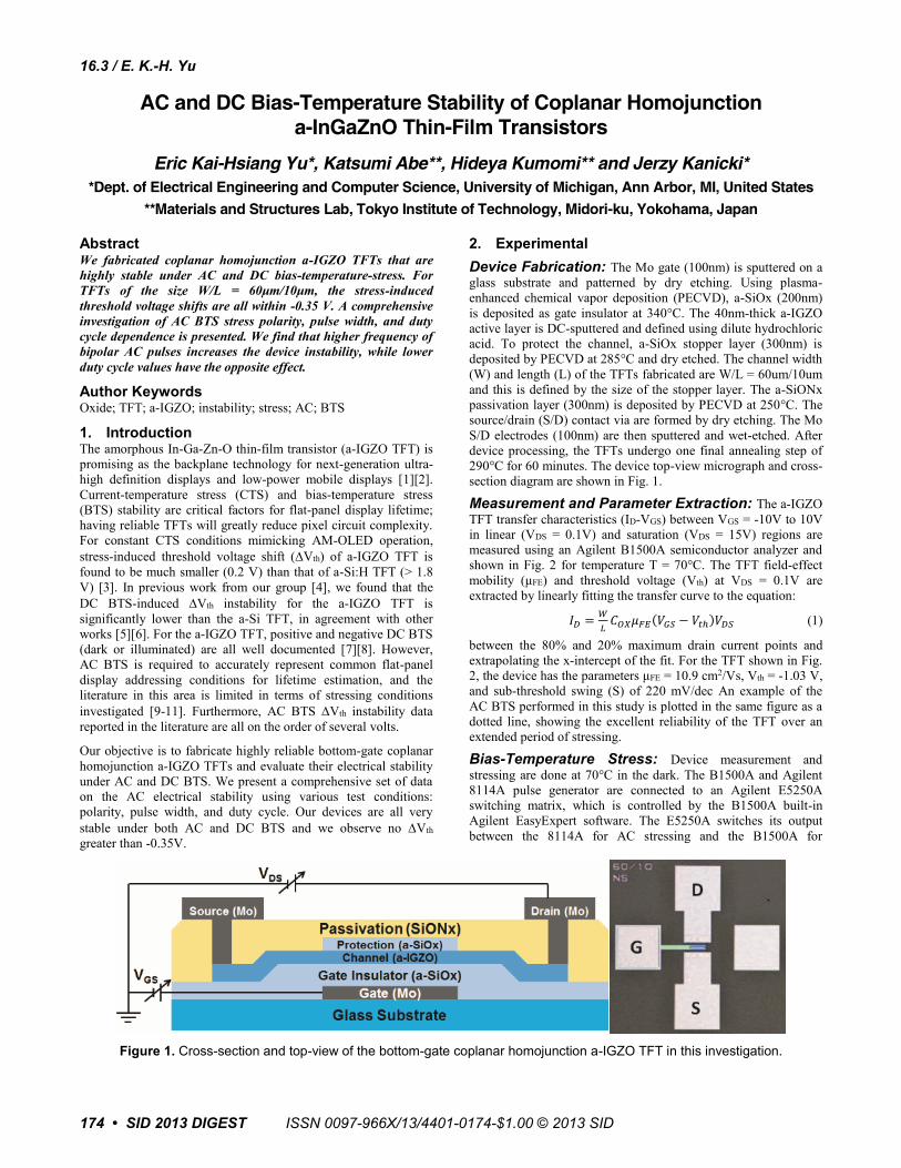
Device Fabrication: The Mo gate (100nm) is sputtered on a
glass substrate and patterned by dry etching. Using plasma-
enhanced chemical vapor deposition (PECVD), a-SiOx (200nm)
is deposited as gate insulator at 340°C. The 40nm-thick a-IGZO
active layer is DC-sputtered and defined using dilute hydrochloric
acid. To protect the channel, a-SiOx stopper layer (300nm) is
deposited by PECVD at 285°C and dry etched. The channel width
(W) and length (L) of the TFTs fabricated are W/L = 60um/10um
and this is defined by the size of the stopper layer. The a-SiONx
passivation layer (300nm) is deposited by PECVD at 250°C. The
source/drain (S/D) contact via are formed by dry etching. The Mo
S/D electrodes (100nm) are then sputtered and wet-etched. After
device processing, the TFTs undergo one final annealing step of
290°C for 60 minutes. The device top-view micrograph and cross-
section diagram are shown in Fig. 1.
Measurement and Parameter Extraction: The a-IGZO
TFT transfer characteristics (ID-VGS) between VGS = -10V to 10V
in linear (VDS = 0.1V) and saturation (VDS = 15V) regions are
measured using an Agilent B1500A semiconductor analyzer and
shown in Fig. 2 for temperature T = 70°C. The TFT field-effect
mobility (μFE) and threshold voltage (Vth) at VDS = 0.1V are
extracted by linearly fitting the transfer curve to the equation:
𝐼𝐷 =𝑊
𝐿𝐶𝑂𝑋𝜇𝐹𝐸(𝑉𝐺𝑆 − 𝑉𝑡ℎ)𝑉𝐷𝑆 (1)
between the 80% and 20% maximum drain current points and
extrapolating the x-intercept of the fit. For the TFT shown in Fig.
2, the device has the parameters μFE = 10.9 cm2/Vs, Vth = -1.03 V,
and sub-threshold swing (S) of 220 mV/dec An example of the
AC BTS performed in this study is plotted in the same figure as a
dotted line, showing the excellent reliability of the TFT over an
extended period of stressing.
Bias-Temperature Stress: Device measurement and
stressing are done at 70°C in the dark. The B1500A and Agilent
8114A pulse generator are connected to an Agilent E5250A
switching matrix, which is controlled by the B1500A built-in
Agilent EasyExpert software. The E5250A switches its output
between the 8114A for AC stressing and the B1500A for
Figure 1. Cross-section and top-view of the bottom-gate coplanar homojunction a-IGZO TFT in this investigation.
ISSN 0097-966X/13/4401-0174-$1.00 © 2013 SID
16.3 / E. K.-H. Yu
174 • SID 2013 DIGEST

Figure 2. The transfer characteristics of the coplanar
homojunction a-IGZO TFTs. Dashed lines indicate the transfer curve shift after 104s of AC BTS.
transfer characteristics measurements. The three types of AC
BTS waveforms used in this study are shown in Fig. 3: positive
unipolar (VG-Stress = 0 to +20V), negative unipolar (0 to -20V),
and bipolar (-20V to +20V). During stressing, the drain and
source are tied together and grounded (VDS = 0V) to ensure a
uniform distribution of the electric field across the channel. The
device stressing is interrupted at set time steps to measure the
transfer characteristics. This repeats until overall accumulated
stress time reaches 104 s. Accumulated stress time is defined as
the total amount of time a non-zero stress bias (positive or
negative) is applied to the gate. A different TFT on the same
wafer is used for each stress condition.
Figure 3. The unipolar and bipolar AC BTS waveforms
used in this investigation.
3. Results and Discussion In Fig. 4, we compare and examine the relationship between DC
and AC bipolar (pulse width PW = 10 ms) BTS instability. We
see that the sum of the positive and negative DC BTS Vth
exceeds that of the bipolar AC BTS, which means that DC BTS
cannot be used to help us understand AC behavior. The bipolar
AC BTS Vth actually falls between the DC BTS values. For the
a-Si TFT, it has been shown that bipolar AC BTS can be
estimated by summing the Vth of positive and negative
unipolar AC BTS segments of equal duration [12]. We confirm
that the same also applies to the a-IGZO TFT in Fig. 5, where
the sum of the unipolar positive and negative AC BTS tracks the
bipolar AC BTS curve very well.
Figure 4. Vth vs. accumulated stress time for bipolar AC
and DC BTS of the a-IGZO TFT (W/L = 60/10). Sum of positive and negative DC BTS is also shown.
Figure 5. The bipolar AC BTS Vth can be approximated
by adding the positive and negative unipolar AC BTS segments of equal accumulated stress time.
In Fig. 6, we change the pulse width for both (a) positive (+20V)
and (b) negative (-20V) unipolar AC BTS. In the case of +20V
AC BTS, the Vth is larger for shorter pulse widths. We also
observe that for all pulse widths, the Vth initially enters a phase
of positive shift for up to 1000s of stressing, and then moves
towards the negative direction for longer stressing. This
phenomenon is similar to the stress-recovery transition reported
for positive BTS of a-IGZO TFTs in the literature [11]. We do
not see any sort of transition for -20V unipolar AC BTS, the
Vth of which are entirely negative and their magnitudes
increase with increasing pulse width.
The relationship between pulse width and instability for -20V
AC BTS is further examined when we normalize Vth for
various pulse widths to the DC BTS shift, and this is shown in
Fig. 7.
16.3 / E. K.-H. Yu
SID 2013 DIGEST • 175
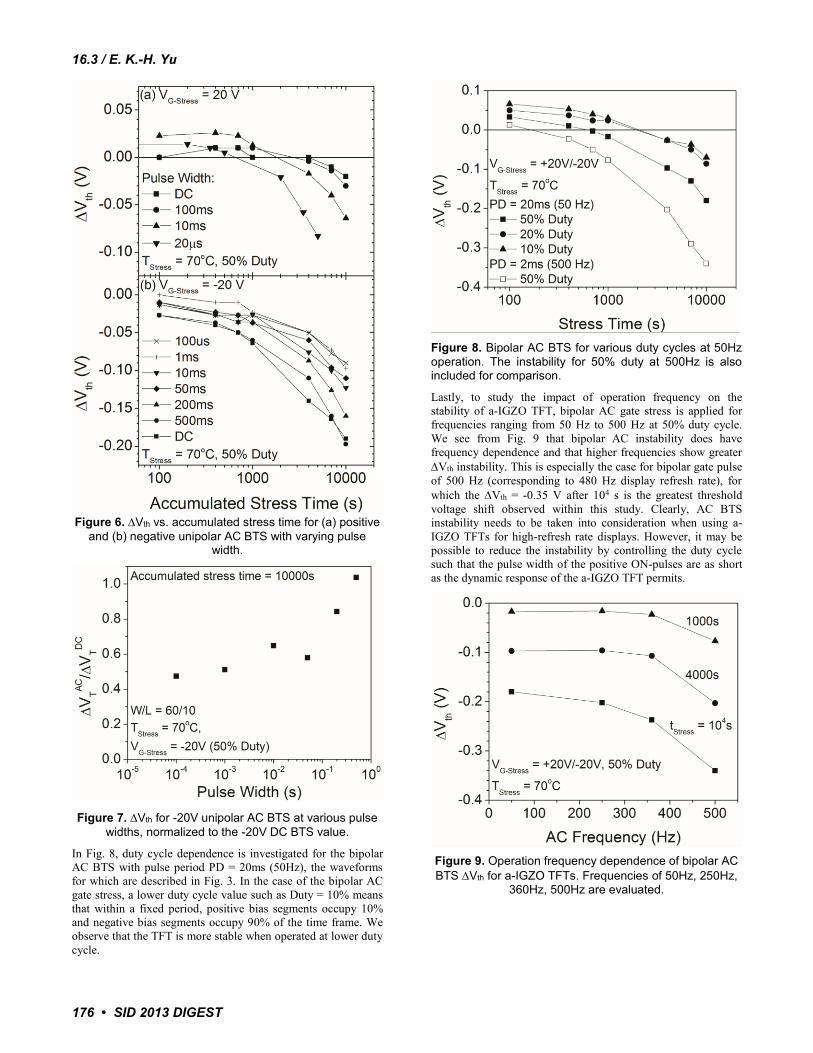
Figure 6. Vth vs. accumulated stress time for (a) positive
and (b) negative unipolar AC BTS with varying pulse width.
Figure 7. Vth for -20V unipolar AC BTS at various pulse
widths, normalized to the -20V DC BTS value.
In Fig. 8, duty cycle dependence is investigated for the bipolar
AC BTS with pulse period PD = 20ms (50Hz), the waveforms
for which are described in Fig. 3. In the case of the bipolar AC
gate stress, a lower duty cycle value such as Duty = 10% means
that within a fixed period, positive bias segments occupy 10%
and negative bias segments occupy 90% of the time frame. We
observe that the TFT is more stable when operated at lower duty
cycle.
Figure 8. Bipolar AC BTS for various duty cycles at 50Hz
operation. The instability for 50% duty at 500Hz is also included for comparison.
Lastly, to study the impact of operation frequency on the
stability of a-IGZO TFT, bipolar AC gate stress is applied for
frequencies ranging from 50 Hz to 500 Hz at 50% duty cycle.
We see from Fig. 9 that bipolar AC instability does have
frequency dependence and that higher frequencies show greater
Vth instability. This is especially the case for bipolar gate pulse
of 500 Hz (corresponding to 480 Hz display refresh rate), for
which the Vth = -0.35 V after 104 s is the greatest threshold
voltage shift observed within this study. Clearly, AC BTS
instability needs to be taken into consideration when using a-
IGZO TFTs for high-refresh rate displays. However, it may be
possible to reduce the instability by controlling the duty cycle
such that the pulse width of the positive ON-pulses are as short
as the dynamic response of the a-IGZO TFT permits.
Figure 9. Operation frequency dependence of bipolar AC
BTS Vth for a-IGZO TFTs. Frequencies of 50Hz, 250Hz, 360Hz, 500Hz are evaluated.
16.3 / E. K.-H. Yu
176 • SID 2013 DIGEST
4. Conclusion We have fabricated high-performance and highly stable bottom-
gate coplanar homojunction a-IGZO TFTs that have a-SiONx as
passivation layer. A comprehensive AC BTS study is conducted
on the TFTs, and they have been demonstrated to be very
reliable under a wide variety of stressing conditions at 70°C.
We find that for our TFTs, the bipolar AC BTS instability time-
evolution can be well-described by a simple sum of the positive
and negative unipolar AC BTS instability, but not the sum of the
DC BTS instabilities. The AC pulse width dependence of the
threshold voltage shift is thoroughly investigated. We find that
negative unipolar pulses exhibit larger (more negative) Vth
shift for longer pulse widths. For positive unipolar pulses, the
Vth are initially positive and eventually trend towards negative
for all pulse widths.
For bipolar AC BTS, we find that instability also has a
dependence on the operation frequency and that higher
frequency causes more instability. This is an important issue
which should be addressed for high-refresh rate displays. Upon
changing the duty cycle of bipolar pulses from 50% to 10%, we
can suppress the Vth for the same frequency. This shows that
different pixel addressing methods, in the form of duty cycle
control, may be viable for improving device stability.
5. Acknowledgements
We would like to thank Qualcomm Inc. for partial financial
support of this study.
6. References [1] K. Nomura, H. Ohta, A. Takagi, T. Kamiya, M. Hirano,
and H. Hosono, “Room-temperature fabrication of
transparent flexible thin-film transistors using amorphous
oxide semiconductors,” Nature 432, No. 7016, 488-492
(2004).
[2] T. Kamiya, K. Nomura, and H. Hosono, “Present Status of
amorphous In-Ga-Zn-O thin-film transistors,” Sci. Technol.
Adv. Mater. 11, 044305 (2010).
[3] C. J. Kim, D. S. Kang, I. Song, J. C. Park, H. Lim, S. Kim,
E. Lee, R. Chung, J. C. Lee, and Y. Park, “Highly stable
Ga2O3-In2O3-ZnO TFT for active-matrix organic light-
emitting diode display application,” in Proc. IEDM, 2006,
pp. 1–4.
[4] T.-C. Fung, K. Abe, H. Kumomi, and J. Kanicki,
“Electrical Instability of RF Sputter Amorphous In-Ga-Zn-
O Thin-Film Transistors,” J. Display Technol. 5, 452
(2009).
[5] J. Y. Kwon, J. S. Sung, K. S. Son, T. S. Kim, M. K. Ryu,
K. B. Park, Y. S. Park, S. Y. Lee, and J. M. Kim,
“GaInZnO TFT for active matrix display,” in AM-FPD ’08
Dig. Tech. Papers, 2008, p-. 287-290.
[6] Y. Ohto, Y. Chikama, T. Hara, Y. Mizuno, T. Aita, M.
Takei, M. Suzuki, O. Nakagawa, Y. Harumoto, H. Nishiki,
and N. Kimura, “Amorphous In-Ga-Zn-O TFT with high
reliability,” in IDW ’09 (The 16th International Display
Workshop), 1685-1688 (2009).
[7] A. Suresh and J. F. Muth, “Bias stress stability of indium
gallium zinc oxide channel based transparent thin film
transistors,” Appl. Phys. Lett. 93, 093504 (2008).
[8] K. Nomura, T. Kamiya, and H. Hosono, “Interface and
bulk effects for bias–light-illumination instability in
amorphous-In-Ga-Zn-O thin-film transistors,” J. Soc. Info.
Display 18, 789 (2010).
[9] T.-C. Fung, K. Abe, H. Kumomi, and J. Kanicki, “DC/AC
Electrical of R.F. Sputter Amorphous In-Ga-Zn-O TFTs,”
in SID Int. Symp. Dig. Tech. Papers 40, 1117 (2009).
[10] S.-J. Kim, S.-Y. Lee, Y. W. Lee, S.-H. Kuk, J.-Y. Kwon,
and M.-K. Han, “Effect of Charge Trapping/Detrapping on
Threshold Voltage Shift of IGZO TFTs under AC Bias
Stress,” Electrochem. Solid-State Lett. 15, H108-H110
(2012).
[11] S.-J. Kim, Y.-W. Lee, S.-Y. Lee, J.-S. Woo, J.- Y. Kwon,
and M.-K. Han, “The Effect of AC Bias Frequency on
Threshold Voltage Shift of the Amorphous Oxide TFTs,”
in SID Int. Symp. Dig. Tech. Papers 42, 1195 (2011).
[12] C. S. Chiang, J. Kanicki, and K. Takechi, “Electrical
Instability of Hydrogenated Amorphous Silicon Thin-Film
Transistors for Active-Matrix Liquid-Crystal Displays,”
Jpn. J. Appl. Phys. 37, 4704-4710 (1998).
16.3 / E. K.-H. Yu
SID 2013 DIGEST • 177