Embed Size (px)
Citation preview
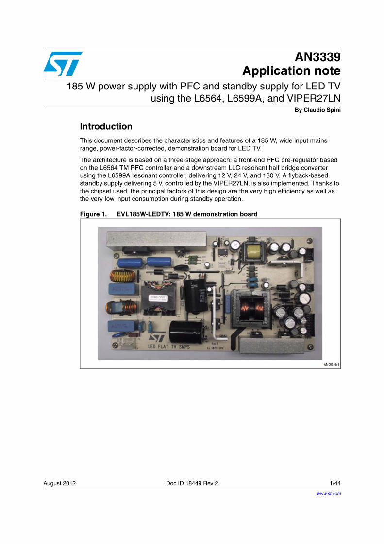
August 2012 Doc ID 18449 Rev 2 1/44
AN3339Application note
185 W power supply with PFC and standby supply for LED TV using the L6564, L6599A, and VIPER27LN
By Claudio Spini
IntroductionThis document describes the characteristics and features of a 185 W, wide input mains range, power-factor-corrected, demonstration board for LED TV.
The architecture is based on a three-stage approach: a front-end PFC pre-regulator based on the L6564 TM PFC controller and a downstream LLC resonant half bridge converter using the L6599A resonant controller, delivering 12 V, 24 V, and 130 V. A flyback-based standby supply delivering 5 V, controlled by the VIPER27LN, is also implemented. Thanks to the chipset used, the principal factors of this design are the very high efficiency as well as the very low input consumption during standby operation.
Figure 1. EVL185W-LEDTV: 185 W demonstration board
www.st.com
Contents AN3339
2/44 Doc ID 18449 Rev 2
Contents
1 Main characteristics and circuit description . . . . . . . . . . . . . . . . . . . . . 6
2 Efficiency measurement . . . . . . . . . . . . . . . . . . . . . . . . . . . . . . . . . . . . . 10
3 Harmonic content measurement . . . . . . . . . . . . . . . . . . . . . . . . . . . . . . 12
4 Functional check . . . . . . . . . . . . . . . . . . . . . . . . . . . . . . . . . . . . . . . . . . . 13
5 Thermal map . . . . . . . . . . . . . . . . . . . . . . . . . . . . . . . . . . . . . . . . . . . . . . 26
6 Conducted emission pre-compliance test . . . . . . . . . . . . . . . . . . . . . . 28
7 Bill of materials . . . . . . . . . . . . . . . . . . . . . . . . . . . . . . . . . . . . . . . . . . . . 29
8 PFC coil specification . . . . . . . . . . . . . . . . . . . . . . . . . . . . . . . . . . . . . . . 36
9 Resonant power transformer specification . . . . . . . . . . . . . . . . . . . . . 38
10 Flyback transformer specification . . . . . . . . . . . . . . . . . . . . . . . . . . . . . 41
11 Revision history . . . . . . . . . . . . . . . . . . . . . . . . . . . . . . . . . . . . . . . . . . . 43
AN3339 List of tables
Doc ID 18449 Rev 2 3/44
List of tables
Table 1. Overall efficiency measured at 230 Vac and 115 Vac mains voltage. . . . . . . . . . . . . . . . . 10Table 2. Thermal maps reference points . . . . . . . . . . . . . . . . . . . . . . . . . . . . . . . . . . . . . . . . . . . . . 27Table 3. Bill of materials . . . . . . . . . . . . . . . . . . . . . . . . . . . . . . . . . . . . . . . . . . . . . . . . . . . . . . . . . . 29Table 4. PFC coil winding data . . . . . . . . . . . . . . . . . . . . . . . . . . . . . . . . . . . . . . . . . . . . . . . . . . . . . 36Table 5. Transformer winding data . . . . . . . . . . . . . . . . . . . . . . . . . . . . . . . . . . . . . . . . . . . . . . . . . . 38Table 6. Transformer winding data . . . . . . . . . . . . . . . . . . . . . . . . . . . . . . . . . . . . . . . . . . . . . . . . . . 41Table 7. Document revision history . . . . . . . . . . . . . . . . . . . . . . . . . . . . . . . . . . . . . . . . . . . . . . . . . 43
List of figures AN3339
4/44 Doc ID 18449 Rev 2
List of figures
Figure 1. EVL185W-LEDTV: 185 W demonstration board . . . . . . . . . . . . . . . . . . . . . . . . . . . . . . . . . 1Figure 2. Electrical diagram . . . . . . . . . . . . . . . . . . . . . . . . . . . . . . . . . . . . . . . . . . . . . . . . . . . . . . . . . 8Figure 3. Standby power supply efficiency . . . . . . . . . . . . . . . . . . . . . . . . . . . . . . . . . . . . . . . . . . . . 10Figure 4. Standby consumption . . . . . . . . . . . . . . . . . . . . . . . . . . . . . . . . . . . . . . . . . . . . . . . . . . . . . 10Figure 5. EN61000-3-2 compliance at 230 Vac - 50 Hz, full load . . . . . . . . . . . . . . . . . . . . . . . . . . . 11Figure 6. JEITA-MITI compliance at 100 Vac - 50 Hz, full load . . . . . . . . . . . . . . . . . . . . . . . . . . . . . 11Figure 7. EN61000-3-2 compliance at 230 Vac - 50 Hz, 75 W . . . . . . . . . . . . . . . . . . . . . . . . . . . . . 11Figure 8. JEITA-MITI compliance at 100 Vac - 50 Hz, 75 W . . . . . . . . . . . . . . . . . . . . . . . . . . . . . . . 11Figure 9. Standby supply waveforms at 115 Vac - 60 Hz - full load . . . . . . . . . . . . . . . . . . . . . . . . . 12Figure 10. Standby supply waveforms at 230 Vac - 50 Hz - full load . . . . . . . . . . . . . . . . . . . . . . . . . 12Figure 11. Standby supply waveforms at 400 Vdc, full load . . . . . . . . . . . . . . . . . . . . . . . . . . . . . . . . 13Figure 12. Standby supply o/p rectifiers PIV at 400 Vdc, full load . . . . . . . . . . . . . . . . . . . . . . . . . . . . 13Figure 13. Standby supply 5 V ripple at 115 Vac - 60 Hz, full load . . . . . . . . . . . . . . . . . . . . . . . . . . . 13Figure 14. Standby supply startup at 115 Vac - 60 Hz, full load . . . . . . . . . . . . . . . . . . . . . . . . . . . . . 13Figure 15. Standby supply burst mode at 230 Vac - 50 Hz, 10 mA load . . . . . . . . . . . . . . . . . . . . . . . 14Figure 16. Standby supply burst mode at 230 Vac, 10 mA load - detail . . . . . . . . . . . . . . . . . . . . . . . 14Figure 17. Standby supply OVP at 115 Vac - 60 Hz, full load . . . . . . . . . . . . . . . . . . . . . . . . . . . . . . . 15Figure 18. Standby supply OVP at 230 Vac - 50 Hz, full load . . . . . . . . . . . . . . . . . . . . . . . . . . . . . . . 15Figure 19. Standby supply OVP at 115 Vac - 60 Hz, 0.5 A load . . . . . . . . . . . . . . . . . . . . . . . . . . . . . 15Figure 20. Standby supply OVP at 115 Vac, 0.5 A load - detail . . . . . . . . . . . . . . . . . . . . . . . . . . . . . 15Figure 21. Standby supply o/p short-circuit at 230 Vac - 50 Hz, full load . . . . . . . . . . . . . . . . . . . . . . 16Figure 22. Standby supply o/p short-circuit at 230 Vac, full load - detail . . . . . . . . . . . . . . . . . . . . . . . 16Figure 23. Standby supply dynamic load at 115 Vac - 60 Hz - PFC off . . . . . . . . . . . . . . . . . . . . . . . . 16Figure 24. Standby supply dynamic load at 115 Vac - 60 Hz - PFC on. . . . . . . . . . . . . . . . . . . . . . . . 16Figure 25. PFC Vds and inductor current at 115 Vac - 60 Hz, full load . . . . . . . . . . . . . . . . . . . . . . . . 17Figure 26. PFC Vds and inductor current at 115 Vac, full load - detail . . . . . . . . . . . . . . . . . . . . . . . . 17Figure 27. PFC Vds and inductor current at 230 Vac - 50 Hz, full load . . . . . . . . . . . . . . . . . . . . . . . . 18Figure 28. PFC Vds and inductor current at 230 Vac, full load - detail . . . . . . . . . . . . . . . . . . . . . . . . 18Figure 29. L6564 signals (1) at 115 Vac - 60 Hz, full load . . . . . . . . . . . . . . . . . . . . . . . . . . . . . . . . . . 18Figure 30. L6564 signals (2) at 115 Vac - 60 Hz, full load . . . . . . . . . . . . . . . . . . . . . . . . . . . . . . . . . . 18Figure 31. Resonant stage waveforms at 115 Vac - 60 Hz, full load . . . . . . . . . . . . . . . . . . . . . . . . . . 19Figure 32. Resonant stage control signals at 115 Vac - 60 Hz, full load . . . . . . . . . . . . . . . . . . . . . . . 19Figure 33. 12 V and 24 V rectifier PIV . . . . . . . . . . . . . . . . . . . . . . . . . . . . . . . . . . . . . . . . . . . . . . . . . 20Figure 34. 130 V rectifier PIV. . . . . . . . . . . . . . . . . . . . . . . . . . . . . . . . . . . . . . . . . . . . . . . . . . . . . . . . 20Figure 35. Startup at full load and 115 Vac by on/off signal . . . . . . . . . . . . . . . . . . . . . . . . . . . . . . . . 20Figure 36. Shut down at full load and 115 Vac by on/off signal . . . . . . . . . . . . . . . . . . . . . . . . . . . . . . 20Figure 37. Startup at full load and 115 Vac by on/off signal - detail. . . . . . . . . . . . . . . . . . . . . . . . . . . 21Figure 38. 12 V load transition . . . . . . . . . . . . . . . . . . . . . . . . . . . . . . . . . . . . . . . . . . . . . . . . . . . . . . . 22Figure 39. 24 V load transition . . . . . . . . . . . . . . . . . . . . . . . . . . . . . . . . . . . . . . . . . . . . . . . . . . . . . . . 22Figure 40. 130 V load transition . . . . . . . . . . . . . . . . . . . . . . . . . . . . . . . . . . . . . . . . . . . . . . . . . . . . . . 22Figure 41. 24 V current limitation at full load and 115 Vac - 60 Hz . . . . . . . . . . . . . . . . . . . . . . . . . . . 23Figure 42. 24 V short-circuit at full load and 115 Vac - 60 Hz . . . . . . . . . . . . . . . . . . . . . . . . . . . . . . . 23Figure 43. 12 V short-circuit at full load and 115 Vac - 60 Hz . . . . . . . . . . . . . . . . . . . . . . . . . . . . . . . 23Figure 44. 130 V short-circuit at full load and 115 Vac - 60 Hz . . . . . . . . . . . . . . . . . . . . . . . . . . . . . . 23Figure 45. OVP at full load and 115 Vac on 24 V output . . . . . . . . . . . . . . . . . . . . . . . . . . . . . . . . . . . 24Figure 46. OVP at full load and 115 Vac on 12 V and 130 V outputs . . . . . . . . . . . . . . . . . . . . . . . . . 24Figure 47. Half cycle mains dip at full load and 115 Vac - 60 Hz. . . . . . . . . . . . . . . . . . . . . . . . . . . . . 24Figure 48. Full cycle mains dip at full load and 115 Vac - 60 Hz . . . . . . . . . . . . . . . . . . . . . . . . . . . . . 24

AN3339 List of figures
Doc ID 18449 Rev 2 5/44
Figure 49. Thermal map at 115 Vac - 60 Hz, full load . . . . . . . . . . . . . . . . . . . . . . . . . . . . . . . . . . . . . 25Figure 50. Thermal map at 230 Vac - 50 Hz, full load . . . . . . . . . . . . . . . . . . . . . . . . . . . . . . . . . . . . . 25Figure 51. CE peak measurement at 115 Vac and full load . . . . . . . . . . . . . . . . . . . . . . . . . . . . . . . . 27Figure 52. CE peak measurement at 230 Vac and full load . . . . . . . . . . . . . . . . . . . . . . . . . . . . . . . . 27Figure 53. PFC coil electrical diagram . . . . . . . . . . . . . . . . . . . . . . . . . . . . . . . . . . . . . . . . . . . . . . . . . 35Figure 54. PFC coil mechanical aspect . . . . . . . . . . . . . . . . . . . . . . . . . . . . . . . . . . . . . . . . . . . . . . . . 36Figure 55. Transformer electrical diagram . . . . . . . . . . . . . . . . . . . . . . . . . . . . . . . . . . . . . . . . . . . . . . 37Figure 56. Transformer overall drawing . . . . . . . . . . . . . . . . . . . . . . . . . . . . . . . . . . . . . . . . . . . . . . . . 38Figure 57. Flyback transformer electrical diagram. . . . . . . . . . . . . . . . . . . . . . . . . . . . . . . . . . . . . . . . 40Figure 58. Flyback transformer overall drawing. . . . . . . . . . . . . . . . . . . . . . . . . . . . . . . . . . . . . . . . . . 41
Main characteristics and circuit description AN3339
6/44 Doc ID 18449 Rev 2
1 Main characteristics and circuit description
The main features of the SMPS are:
● Universal input mains range: 90 ÷ 264 Vac - frequency 45 ÷ 65 Hz
● Output voltage 1: 130 V ±8 % at 620 mA for backlight
● Output voltage 2: 24 V ±8 % at 2 A for audio supply
● Output voltage 3: 12 V ±1 % at 4 A for panel supply
● Output voltage 4: 5 V ±2 % at 2 A for microprocessor supply
● Mains harmonics: acc. to EN61000-3-2 Class-D or JEITA-MITI Class-D
● Standby mains consumption: <170 mW at 230 Vac with 50 mW load
● Overall efficiency at full load: >90 %
● EMI: acc. to EN55022-Class-B
● Safety: acc. to EN60065
● Dimensions: 115x204 mm, 25 mm maximum component height from PCB
● PCB: single side, 70 µm, CEM-1, mixed PTH/SMT
The circuit is made up of two sections: a 10 W standby supply delivering 5 V, dedicated to supplying the microprocessor and the logic circuitry, and a bigger section made up of a front-end PFC and an LLC resonant converter delivering three output voltages, 12 V is dedicated to supplying the TV panel, 24 V to supplying the audio power amplifiers and 130 V is dedicated to the backlight.
The PFC stage delivers 400 V constant voltage and acts as the pre-regulator for both the LLC stage and the standby supply.
An external signal, referred to secondary ground, turns the PFC and the LLC stage on and off.
Startup
At turn-on the standby supply begins startup and delivers 5 V dedicated to the TV microprocessor and other logic circuitry. It also generates the auxiliary voltage powering the PFC and LLC controllers at primary side via the linear regulator Q7. Q7 is activated by the optocoupler U5 that is driven by the logic signal on/off. At startup, the on/off signal (active high) from the microprocessor is supposed to be low, so the PFC and the LLC do not work.
Once the on/off signal is asserted high, the regulator Q7 delivers 14 V powering the PFC controller L6564 and the LLC controller L6599A; to always ensure proper operation of the LLC, the circuit is designed so that the PFC starts first, then the downstream converter. The LINE pin of L6599A allows the resonant stage to operate only if the PFC output is delivering its rated output voltage. It prevents the resonant converter from working with too low input voltage that can cause undesirable capacitive mode operation.
The L6599A LINE pin internal comparator has a hysteresis which allows to independently set the turn-on and turn-off voltage. The LLC turn-on voltage (PFC output) has been set to 380 V while the turn-off threshold has been set to 300 V. This last value avoids capacitive mode operation by the LLC stage but allows the resonant stage to operate even in the case of mains sag and consequent lowering of PFC output voltage.
AN3339 Main characteristics and circuit description
Doc ID 18449 Rev 2 7/44
Brownout protection
Brownout protection prevents the circuit from working with abnormal mains levels. It is achieved by two separate circuits, one using the brownout pin of the VIPer® and a second using an internal comparator of the L6564 dedicated to this function: this pin is internally connected to the VFF pin (#5) providing the information of the mains voltage peak value. The internal comparator allows the IC operations if the mains level is correct, within the nominal limits.
If the input voltage is below ~80 Vac (typ.), circuit startup is not allowed.
Resonant power stage
The downstream converter featuring the ST L6599A, incorporates all the functions necessary to properly drive the resonant converter with a 50 % fixed duty cycle and works with variable frequency.
The transformer, using the integrated magnetic approach and incorporating the resonant series inductance, delivers 3 output voltages without any post-regulator.
The transformer configuration chosen for the secondary winding delivering 12 V and 24 V output is center-tap and makes use of power Schottky rectifiers. For the secondary winding delivering 130 V, a full bridge configuration using four ultrafast diodes has been chosen. A small LC filter has been added on each output, to filter the high frequency ripple.
Output voltage feedback loop
The resonant stage feedback loop is implemented by means of a typical circuit using a TL431 modulating the current in the optocoupler diode. The three outputs are regulated by a weighted feedback control.
On the primary side, R37 - connecting the RFMIN pin (#4) to the optocoupler's phototransistor - closes the feedback loop and its value sets the maximum switching frequency. R36, connecting the same pin to ground, sets the minimum switching frequency. The RC series R22 and C21 sets both soft-start maximum frequency and duration.
L6599A overload and short-circuit protection
The current into the primary winding is sensed by the loss-less circuit R53, C36, D14, D12, R55, and C38, and is fed into the ISEN pin (#6). In the case of overcurrent, the voltage on the pin overpass the internal comparator threshold (0.8 V), triggering a protection sequence. The capacitor (C37) connected to the DELAY pin (#2) is charged by an internal 150 µA current generator and is slowly discharged by the resistor R54. This pin is connected to the DIS pin and as soon as the voltage achieves 1.85 V, the IC stops switching latched. On/off signal recycling is necessary to restart the resonant converter.
Overvoltage and open loop protection
Both PFC and resonant stages are equipped with their own overvoltage protection.
The PFC controller L6564 monitors its output voltage via the resistor divider connected to the PFC_OK pin (#6) protecting the circuit in case of loop failures, disconnection, or deviation from the nominal value of the feedback loop divider. When a fault condition is detected, by monitoring both PFC_OK and INV pins, the PFC_OK circuitry latches the L6564 operations. The PFC is kept latched until the mains voltage is recycled.
In the case of overvoltage by the resonant stage the Zener diodes D16, D17, and D29 detect the output voltages and conduct. This causes Q10 to turn on and, consequently, Q9

Main characteristics and circuit description AN3339
8/44 Doc ID 18449 Rev 2
also turns on. These two transistors form an SCR structure that shorts to ground the anode of the U5 optocoupler in case of an overvoltage event. In this way, Q7 cannot deliver supply voltage Vcc to the controller which remains latched until the mains voltage is recycled.
To protect the PFC and LLC controllers from being powered with an abnormal voltage, which may occur in the case of a failure of the regulator based on Q7, an overvoltage protection is provided by the Zener diode D13. In the case of the Q7 regulator providing an excessive output voltage, D13 is reverse-biased and latches the L6599A through the DIS pin (#8).
AN3339 Main characteristics and circuit description
Doc ID 18449 Rev 2 9/44
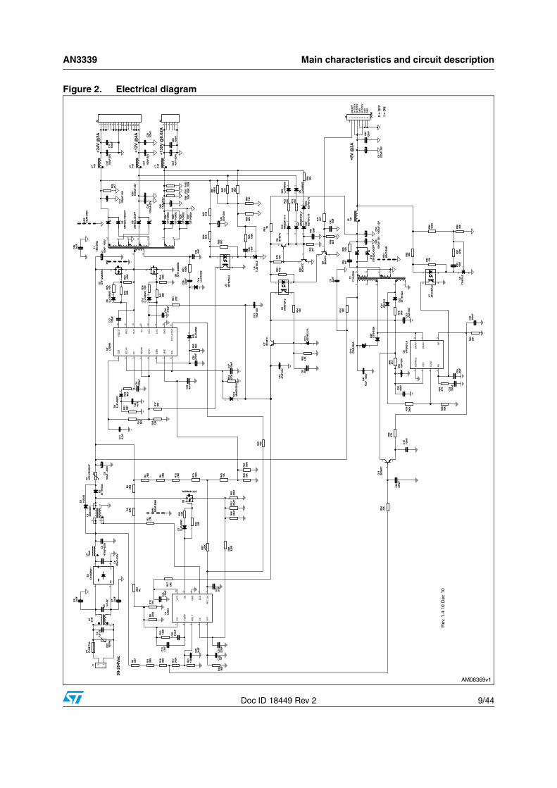
Figure 2. Electrical diagram
Efficiency measurement AN3339
10/44 Doc ID 18449 Rev 2
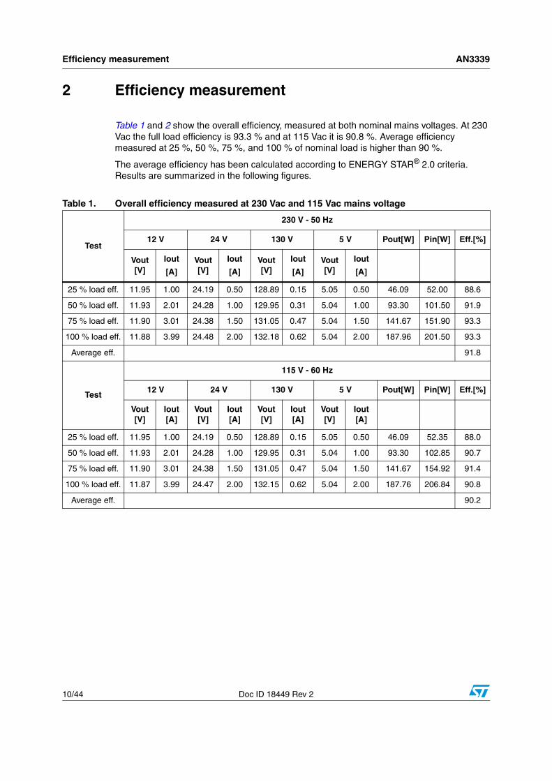
2 Efficiency measurement
Table 1 and 2 show the overall efficiency, measured at both nominal mains voltages. At 230 Vac the full load efficiency is 93.3 % and at 115 Vac it is 90.8 %. Average efficiency measured at 25 %, 50 %, 75 %, and 100 % of nominal load is higher than 90 %.
The average efficiency has been calculated according to ENERGY STAR® 2.0 criteria. Results are summarized in the following figures.
Table 1. Overall efficiency measured at 230 Vac and 115 Vac mains voltage
Test
230 V - 50 Hz
12 V 24 V 130 V 5 V Pout[W] Pin[W] Eff.[%]
Vout [V]
Iout
[A]Vout [V]
Iout
[A]Vout [V]
Iout
[A]Vout [V]
Iout
[A]
25 % load eff. 11.95 1.00 24.19 0.50 128.89 0.15 5.05 0.50 46.09 52.00 88.6
50 % load eff. 11.93 2.01 24.28 1.00 129.95 0.31 5.04 1.00 93.30 101.50 91.9
75 % load eff. 11.90 3.01 24.38 1.50 131.05 0.47 5.04 1.50 141.67 151.90 93.3
100 % load eff. 11.88 3.99 24.48 2.00 132.18 0.62 5.04 2.00 187.96 201.50 93.3
Average eff. 91.8
Test
115 V - 60 Hz
12 V 24 V 130 V 5 V Pout[W] Pin[W] Eff.[%]
Vout [V]
Iout [A]
Vout [V]
Iout [A]
Vout [V]
Iout [A]
Vout [V]
Iout [A]
25 % load eff. 11.95 1.00 24.19 0.50 128.89 0.15 5.05 0.50 46.09 52.35 88.0
50 % load eff. 11.93 2.01 24.28 1.00 129.95 0.31 5.04 1.00 93.30 102.85 90.7
75 % load eff. 11.90 3.01 24.38 1.50 131.05 0.47 5.04 1.50 141.67 154.92 91.4
100 % load eff. 11.87 3.99 24.47 2.00 132.15 0.62 5.04 2.00 187.76 206.84 90.8
Average eff. 90.2
AN3339 Efficiency measurement
Doc ID 18449 Rev 2 11/44
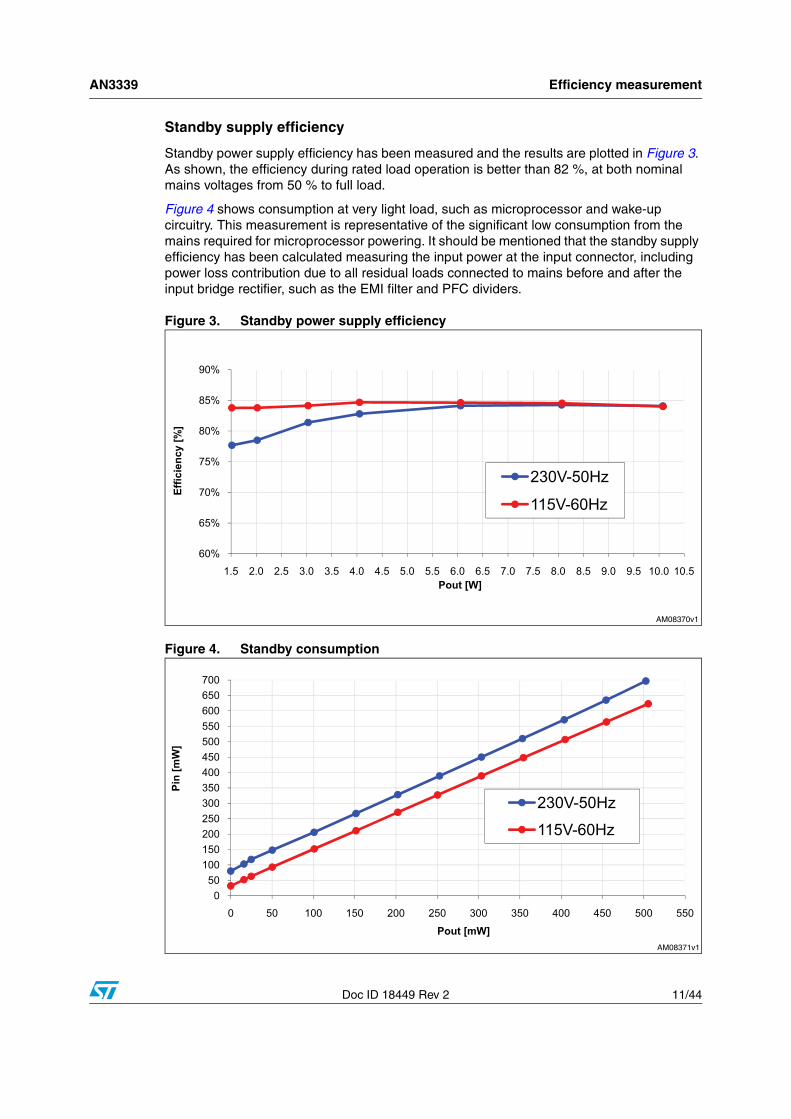
Standby supply efficiency
Standby power supply efficiency has been measured and the results are plotted in Figure 3. As shown, the efficiency during rated load operation is better than 82 %, at both nominal mains voltages from 50 % to full load.
Figure 4 shows consumption at very light load, such as microprocessor and wake-up circuitry. This measurement is representative of the significant low consumption from the mains required for microprocessor powering. It should be mentioned that the standby supply efficiency has been calculated measuring the input power at the input connector, including power loss contribution due to all residual loads connected to mains before and after the input bridge rectifier, such as the EMI filter and PFC dividers.
Figure 3. Standby power supply efficiency
Figure 4. Standby consumption
Harmonic content measurement AN3339
12/44 Doc ID 18449 Rev 2
3 Harmonic content measurement
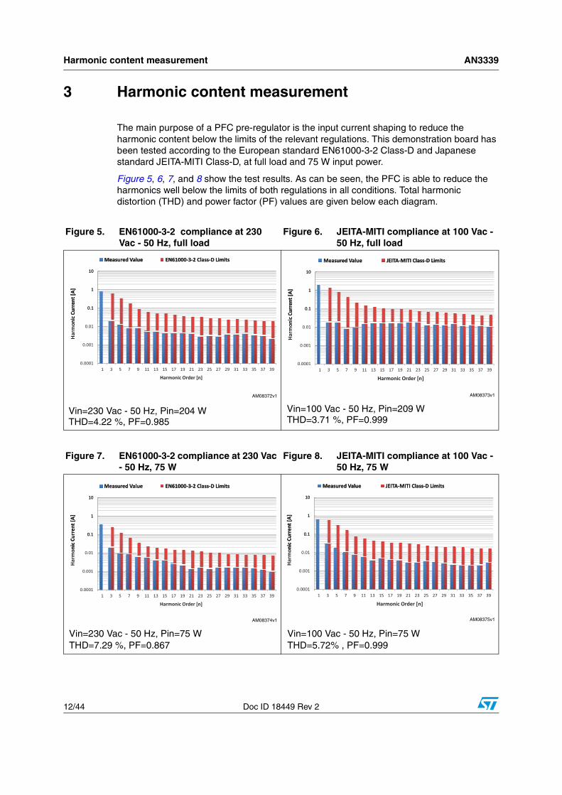
The main purpose of a PFC pre-regulator is the input current shaping to reduce the harmonic content below the limits of the relevant regulations. This demonstration board has been tested according to the European standard EN61000-3-2 Class-D and Japanese standard JEITA-MITI Class-D, at full load and 75 W input power.
Figure 5, 6, 7, and 8 show the test results. As can be seen, the PFC is able to reduce the harmonics well below the limits of both regulations in all conditions. Total harmonic distortion (THD) and power factor (PF) values are given below each diagram.
Figure 5. EN61000-3-2 compliance at 230 Vac - 50 Hz, full load
Figure 6. JEITA-MITI compliance at 100 Vac - 50 Hz, full load
Vin=230 Vac - 50 Hz, Pin=204 WTHD=4.22 %, PF=0.985
AM08372v1
0.1
1
10
onic
Cur
rent
[A]
Measured Value EN61000-3-2 Class-D Limits
0.0001
0.001
0.01
0.1
1
10
1 3 5 7 9 11 13 15 17 19 21 23 25 27 29 31 33 35 37 39
Har
mon
ic C
urre
nt [A
]
Harmonic Order [n]
Measured Value EN61000-3-2 Class-D Limits
Vin=100 Vac - 50 Hz, Pin=209 WTHD=3.71 %, PF=0.999
AM08373v1
0.1
1
10
onic
Cur
rent
[A]
Measured Value JEITA-MITI Class-D Limits
0.0001
0.001
0.01
0.1
1
10
1 3 5 7 9 11 13 15 17 19 21 23 25 27 29 31 33 35 37 39
Har
mon
ic C
urre
nt [A
]
Harmonic Order [n]
Measured Value JEITA-MITI Class-D Limits
Figure 7. EN61000-3-2 compliance at 230 Vac - 50 Hz, 75 W
Figure 8. JEITA-MITI compliance at 100 Vac - 50 Hz, 75 W
Vin=230 Vac - 50 Hz, Pin=75 WTHD=7.29 %, PF=0.867
AM08374v1
0.1
1
10
onic
Cur
rent
[A]
Measured Value EN61000-3-2 Class-D Limits
0.0001
0.001
0.01
0.1
1
10
1 3 5 7 9 11 13 15 17 19 21 23 25 27 29 31 33 35 37 39
Har
mon
ic C
urre
nt [A
]
Harmonic Order [n]
Measured Value EN61000-3-2 Class-D Limits
Vin=100 Vac - 50 Hz, Pin=75 WTHD=5.72% , PF=0.999
AM08375v1
0.1
1
10
o nic
Cur
rent
[A]
Measured Value JEITA-MITI Class-D Limits
0.0001
0.001
0.01
0.1
1
10
1 3 5 7 9 11 13 15 17 19 21 23 25 27 29 31 33 35 37 39
Har
mon
ic C
urre
nt [A
]
Harmonic Order [n]
Measured Value JEITA-MITI Class-D Limits
AN3339 Functional check
Doc ID 18449 Rev 2 13/44
4 Functional check
Standby supply
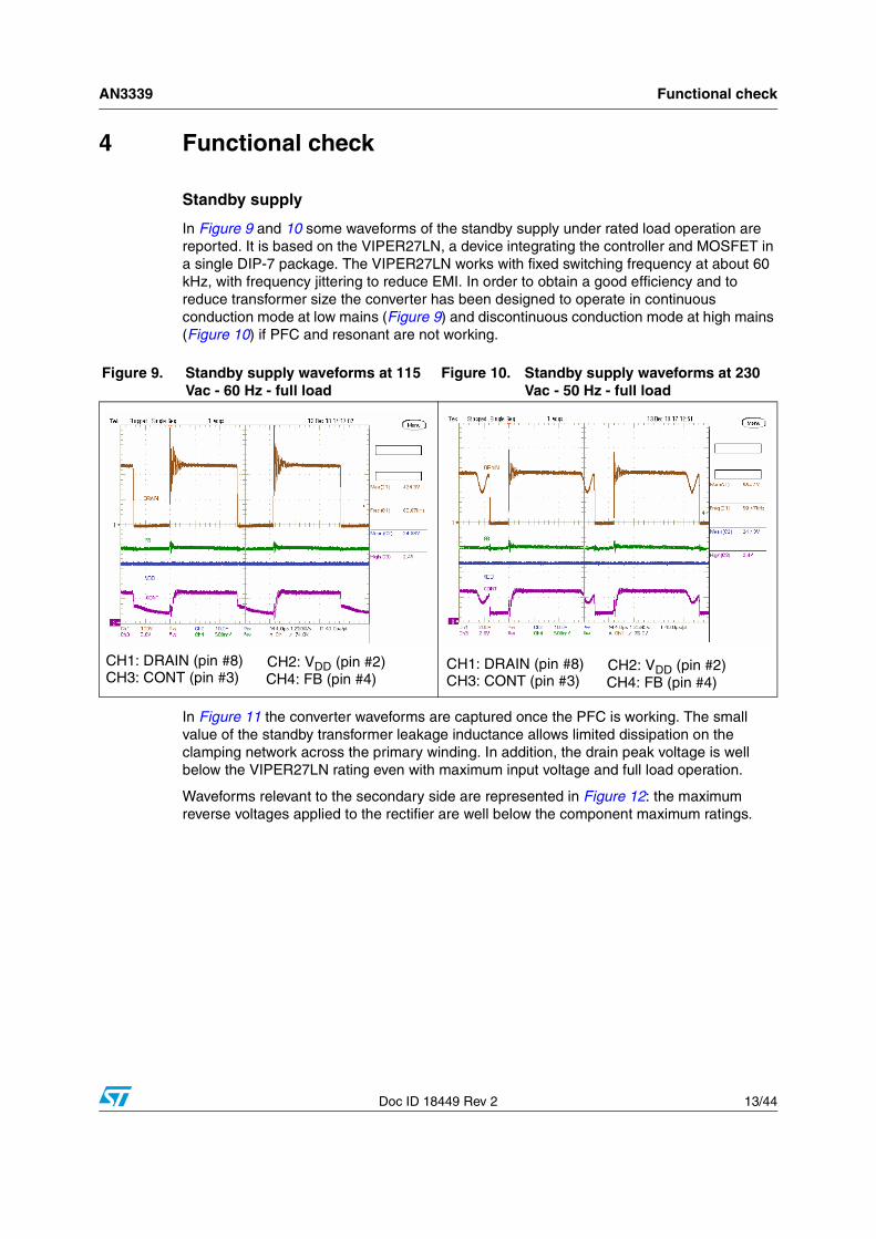
In Figure 9 and 10 some waveforms of the standby supply under rated load operation are reported. It is based on the VIPER27LN, a device integrating the controller and MOSFET in a single DIP-7 package. The VIPER27LN works with fixed switching frequency at about 60 kHz, with frequency jittering to reduce EMI. In order to obtain a good efficiency and to reduce transformer size the converter has been designed to operate in continuous conduction mode at low mains (Figure 9) and discontinuous conduction mode at high mains (Figure 10) if PFC and resonant are not working.
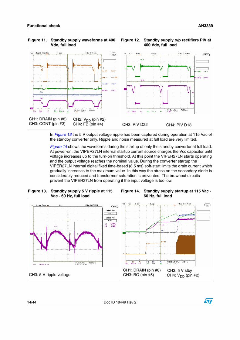
In Figure 11 the converter waveforms are captured once the PFC is working. The small value of the standby transformer leakage inductance allows limited dissipation on the clamping network across the primary winding. In addition, the drain peak voltage is well below the VIPER27LN rating even with maximum input voltage and full load operation.
Waveforms relevant to the secondary side are represented in Figure 12: the maximum reverse voltages applied to the rectifier are well below the component maximum ratings.
Figure 9. Standby supply waveforms at 115 Vac - 60 Hz - full load
Figure 10. Standby supply waveforms at 230 Vac - 50 Hz - full load
CH2: VDD (pin #2)CH1: DRAIN (pin #8)CH3: CONT (pin #3) CH4: FB (pin #4)
CH2: VDD (pin #2)CH1: DRAIN (pin #8)CH3: CONT (pin #3) CH4: FB (pin #4)
Functional check AN3339
14/44 Doc ID 18449 Rev 2
In Figure 13 the 5 V output voltage ripple has been captured during operation at 115 Vac of the standby converter only. Ripple and noise measured at full load are very limited.
Figure 14 shows the waveforms during the startup of only the standby converter at full load. At power-on, the VIPER27LN internal startup current source charges the Vcc capacitor until voltage increases up to the turn-on threshold. At this point the VIPER27LN starts operating and the output voltage reaches the nominal value. During the converter startup the VIPER27LN internal digital fixed time-based (8.5 ms) soft-start limits the drain current which gradually increases to the maximum value. In this way the stress on the secondary diode is considerably reduced and transformer saturation is prevented. The brownout circuits prevent the VIPER27LN from operating if the input voltage is too low.
Figure 11. Standby supply waveforms at 400 Vdc, full load
Figure 12. Standby supply o/p rectifiers PIV at 400 Vdc, full load
CH2: VDD (pin #2)CH1: DRAIN (pin #8)CH3: CONT (pin #3) CH4: FB (pin #4) CH3: PIV D22 CH4: PIV D18
Figure 13. Standby supply 5 V ripple at 115 Vac - 60 Hz, full load
Figure 14. Standby supply startup at 115 Vac - 60 Hz, full load
CH3: 5 V ripple voltageCH2: 5 V stbyCH1: DRAIN (pin #8)
CH3: BO (pin #5) CH4: VDD (pin #2)
AN3339 Functional check
Doc ID 18449 Rev 2 15/44
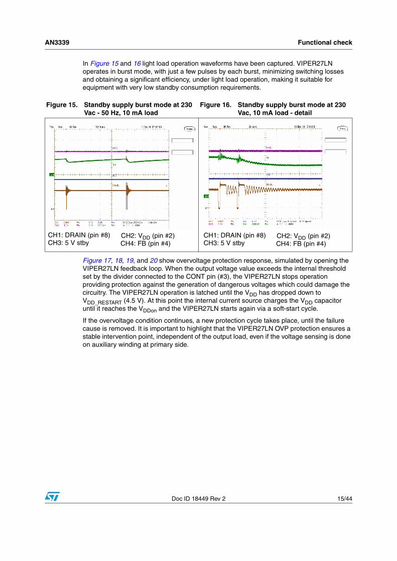
In Figure 15 and 16 light load operation waveforms have been captured. VIPER27LN operates in burst mode, with just a few pulses by each burst, minimizing switching losses and obtaining a significant efficiency, under light load operation, making it suitable for equipment with very low standby consumption requirements.
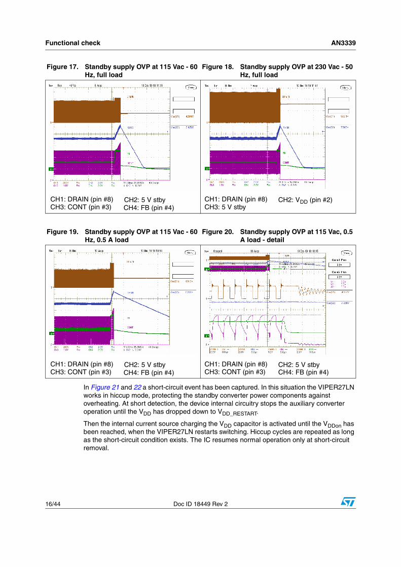
Figure 17, 18, 19, and 20 show overvoltage protection response, simulated by opening the VIPER27LN feedback loop. When the output voltage value exceeds the internal threshold set by the divider connected to the CONT pin (#3), the VIPER27LN stops operation providing protection against the generation of dangerous voltages which could damage the circuitry. The VIPER27LN operation is latched until the VDD has dropped down to VDD_RESTART (4.5 V). At this point the internal current source charges the VDD capacitor until it reaches the VDDon and the VIPER27LN starts again via a soft-start cycle.
If the overvoltage condition continues, a new protection cycle takes place, until the failure cause is removed. It is important to highlight that the VIPER27LN OVP protection ensures a stable intervention point, independent of the output load, even if the voltage sensing is done on auxiliary winding at primary side.
Figure 15. Standby supply burst mode at 230 Vac - 50 Hz, 10 mA load
Figure 16. Standby supply burst mode at 230 Vac, 10 mA load - detail
CH2: VDD (pin #2)CH1: DRAIN (pin #8)CH3: 5 V stby CH4: FB (pin #4)
CH2: VDD (pin #2)CH1: DRAIN (pin #8)CH3: 5 V stby CH4: FB (pin #4)
Functional check AN3339
16/44 Doc ID 18449 Rev 2
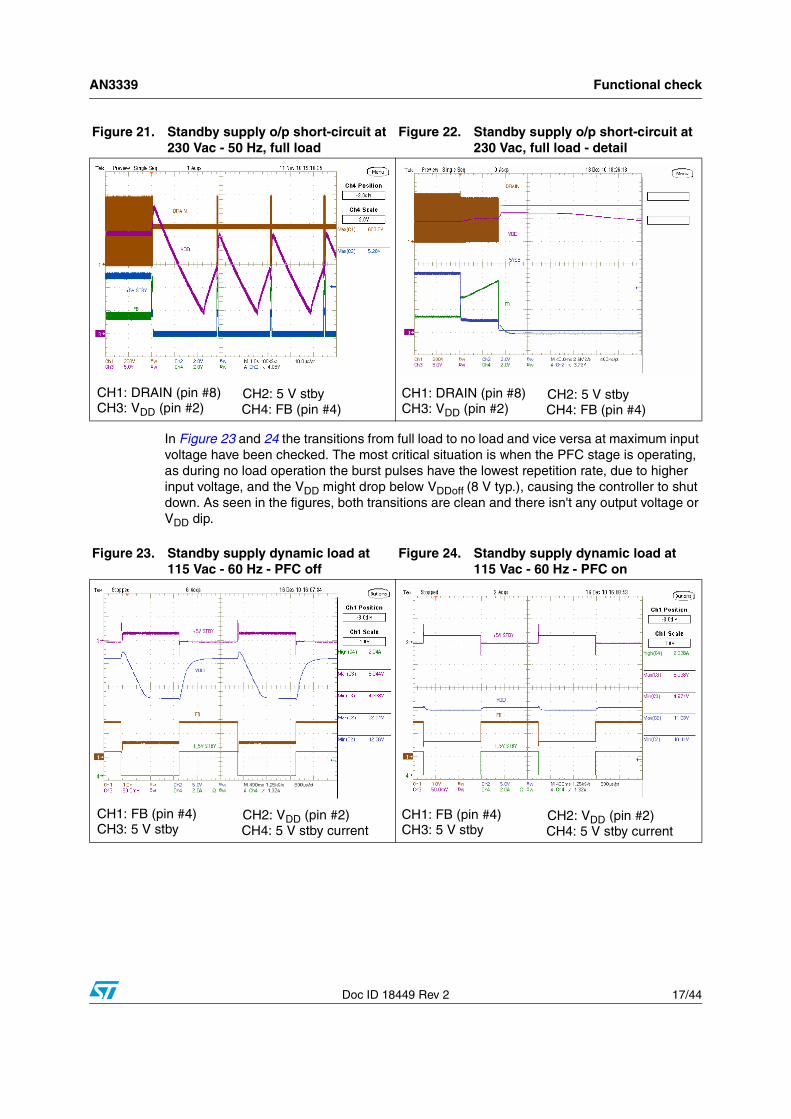
In Figure 21 and 22 a short-circuit event has been captured. In this situation the VIPER27LN works in hiccup mode, protecting the standby converter power components against overheating. At short detection, the device internal circuitry stops the auxiliary converter operation until the VDD has dropped down to VDD_RESTART.
Then the internal current source charging the VDD capacitor is activated until the VDDon has been reached, when the VIPER27LN restarts switching. Hiccup cycles are repeated as long as the short-circuit condition exists. The IC resumes normal operation only at short-circuit removal.
Figure 17. Standby supply OVP at 115 Vac - 60 Hz, full load
Figure 18. Standby supply OVP at 230 Vac - 50 Hz, full load
CH2: 5 V stbyCH1: DRAIN (pin #8)CH3: CONT (pin #3) CH4: FB (pin #4)
CH2: VDD (pin #2)CH1: DRAIN (pin #8)CH3: 5 V stby
Figure 19. Standby supply OVP at 115 Vac - 60 Hz, 0.5 A load
Figure 20. Standby supply OVP at 115 Vac, 0.5 A load - detail
CH2: 5 V stbyCH1: DRAIN (pin #8)CH3: CONT (pin #3) CH4: FB (pin #4)
CH2: 5 V stbyCH1: DRAIN (pin #8)CH3: CONT (pin #3) CH4: FB (pin #4)
AN3339 Functional check
Doc ID 18449 Rev 2 17/44
In Figure 23 and 24 the transitions from full load to no load and vice versa at maximum input voltage have been checked. The most critical situation is when the PFC stage is operating, as during no load operation the burst pulses have the lowest repetition rate, due to higher input voltage, and the VDD might drop below VDDoff (8 V typ.), causing the controller to shut down. As seen in the figures, both transitions are clean and there isn't any output voltage or VDD dip.
Figure 21. Standby supply o/p short-circuit at 230 Vac - 50 Hz, full load
Figure 22. Standby supply o/p short-circuit at 230 Vac, full load - detail
CH2: 5 V stbyCH1: DRAIN (pin #8)CH3: VDD (pin #2) CH4: FB (pin #4)
CH2: 5 V stbyCH1: DRAIN (pin #8)CH3: VDD (pin #2) CH4: FB (pin #4)
Figure 23. Standby supply dynamic load at 115 Vac - 60 Hz - PFC off
Figure 24. Standby supply dynamic load at 115 Vac - 60 Hz - PFC on
CH2: VDD (pin #2)CH1: FB (pin #4)CH3: 5 V stby CH4: 5 V stby current
CH2: VDD (pin #2)CH1: FB (pin #4)CH3: 5 V stby CH4: 5 V stby current
Functional check AN3339
18/44 Doc ID 18449 Rev 2
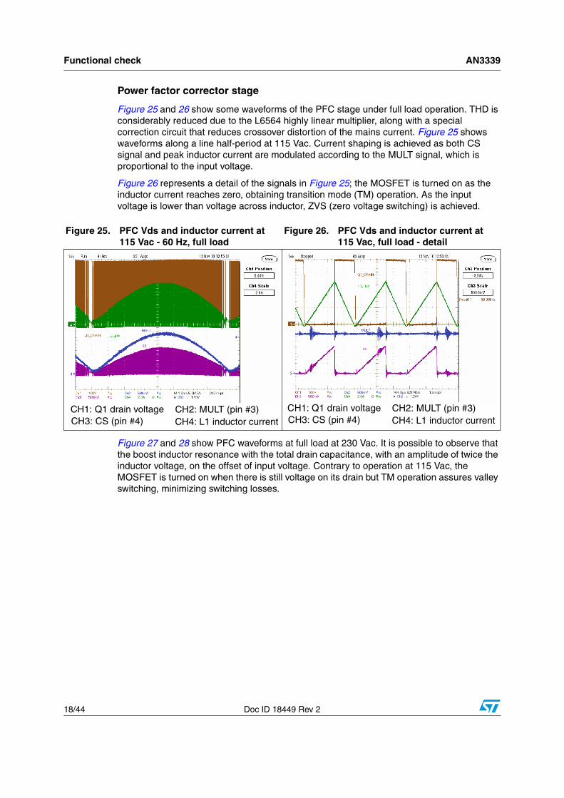
Power factor corrector stage
Figure 25 and 26 show some waveforms of the PFC stage under full load operation. THD is considerably reduced due to the L6564 highly linear multiplier, along with a special correction circuit that reduces crossover distortion of the mains current. Figure 25 shows waveforms along a line half-period at 115 Vac. Current shaping is achieved as both CS signal and peak inductor current are modulated according to the MULT signal, which is proportional to the input voltage.
Figure 26 represents a detail of the signals in Figure 25; the MOSFET is turned on as the inductor current reaches zero, obtaining transition mode (TM) operation. As the input voltage is lower than voltage across inductor, ZVS (zero voltage switching) is achieved.
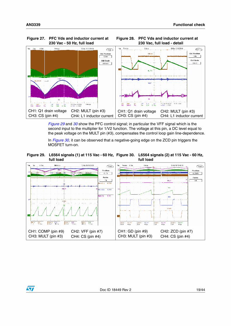
Figure 27 and 28 show PFC waveforms at full load at 230 Vac. It is possible to observe that the boost inductor resonance with the total drain capacitance, with an amplitude of twice the inductor voltage, on the offset of input voltage. Contrary to operation at 115 Vac, the MOSFET is turned on when there is still voltage on its drain but TM operation assures valley switching, minimizing switching losses.
Figure 25. PFC Vds and inductor current at 115 Vac - 60 Hz, full load
Figure 26. PFC Vds and inductor current at 115 Vac, full load - detail
CH3: CS (pin #4)CH1: Q1 drain voltage CH2: MULT (pin #3)
CH4: L1 inductor current CH3: CS (pin #4)CH1: Q1 drain voltage CH2: MULT (pin #3)
CH4: L1 inductor current
AN3339 Functional check
Doc ID 18449 Rev 2 19/44
Figure 29 and 30 show the PFC control signal; in particular the VFF signal which is the second input to the multiplier for 1/V2 function. The voltage at this pin, a DC level equal to the peak voltage on the MULT pin (#3), compensates the control loop gain line-dependence.
In Figure 30, it can be observed that a negative-going edge on the ZCD pin triggers the MOSFET turn-on.
Figure 27. PFC Vds and inductor current at 230 Vac - 50 Hz, full load
Figure 28. PFC Vds and inductor current at 230 Vac, full load - detail
CH3: CS (pin #4)CH1: Q1 drain voltage CH2: MULT (pin #3)
CH4: L1 inductor current CH3: CS (pin #4)CH1: Q1 drain voltage CH2: MULT (pin #3)
CH4: L1 inductor current
Figure 29. L6564 signals (1) at 115 Vac - 60 Hz, full load
Figure 30. L6564 signals (2) at 115 Vac - 60 Hz, full load
CH3: MULT (pin #3)CH1: COMP (pin #9) CH2: VFF (pin #7)
CH4: CS (pin #4) CH3: MULT (pin #3)CH1: GD (pin #9) CH2: ZCD (pin #7)
CH4: CS (pin #4)
Functional check AN3339
20/44 Doc ID 18449 Rev 2
Resonant stage
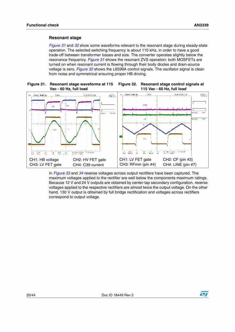
Figure 31 and 32 show some waveforms relevant to the resonant stage during steady-state operation. The selected switching frequency is about 110 kHz, in order to have a good trade-off between transformer losses and size. The converter operates slightly below the resonance frequency. Figure 31 shows the resonant ZVS operation: both MOSFETs are turned on when resonant current is flowing through their body diodes and drain-source voltage is zero. Figure 32 shows the L6599A control signals. The oscillator signal is clean from noise and symmetrical ensuring proper HB driving.
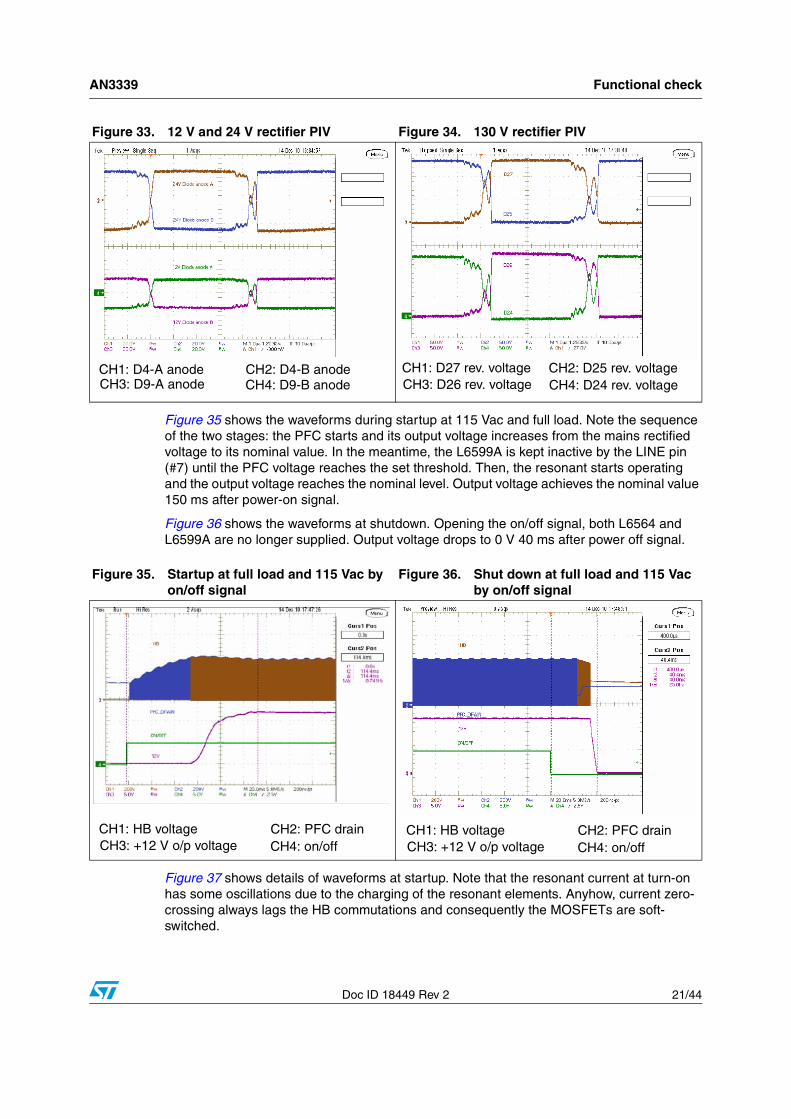
In Figure 33 and 34 reverse voltages across output rectifiers have been captured. The maximum voltages applied to the rectifier are well below the components maximum ratings. Because 12 V and 24 V outputs are obtained by center-tap secondary configuration, reverse voltages applied to the respective rectifiers are almost twice the output voltage. On the other hand, 130 V output is obtained by full bridge rectification and voltages across rectifiers correspond to output voltage.
Figure 31. Resonant stage waveforms at 115 Vac - 60 Hz, full load
Figure 32. Resonant stage control signals at 115 Vac - 60 Hz, full load
CH3: LV FET gateCH1: HB voltage CH2: HV FET gate
CH4: C39 current CH3: RFmin (pin #4)CH1: LV FET gate CH2: CF (pin #3)
CH4: LINE (pin #7)
AN3339 Functional check
Doc ID 18449 Rev 2 21/44
Figure 35 shows the waveforms during startup at 115 Vac and full load. Note the sequence of the two stages: the PFC starts and its output voltage increases from the mains rectified voltage to its nominal value. In the meantime, the L6599A is kept inactive by the LINE pin (#7) until the PFC voltage reaches the set threshold. Then, the resonant starts operating and the output voltage reaches the nominal level. Output voltage achieves the nominal value 150 ms after power-on signal.
Figure 36 shows the waveforms at shutdown. Opening the on/off signal, both L6564 and L6599A are no longer supplied. Output voltage drops to 0 V 40 ms after power off signal.
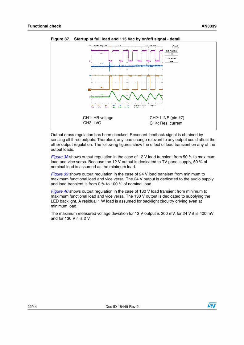
Figure 37 shows details of waveforms at startup. Note that the resonant current at turn-on has some oscillations due to the charging of the resonant elements. Anyhow, current zero-crossing always lags the HB commutations and consequently the MOSFETs are soft-switched.
Figure 33. 12 V and 24 V rectifier PIV Figure 34. 130 V rectifier PIV
CH3: D9-A anodeCH1: D4-A anode CH2: D4-B anode
CH4: D9-B anode CH3: D26 rev. voltageCH1: D27 rev. voltage CH2: D25 rev. voltage
CH4: D24 rev. voltage
Figure 35. Startup at full load and 115 Vac by on/off signal
Figure 36. Shut down at full load and 115 Vac by on/off signal
CH3: +12 V o/p voltageCH1: HB voltage CH2: PFC drain
CH4: on/off CH3: +12 V o/p voltageCH1: HB voltage CH2: PFC drain
CH4: on/off
Functional check AN3339
22/44 Doc ID 18449 Rev 2
Figure 37. Startup at full load and 115 Vac by on/off signal - detail
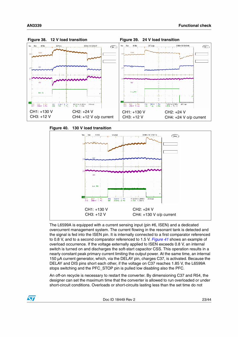
Output cross regulation has been checked. Resonant feedback signal is obtained by sensing all three outputs. Therefore, any load change relevant to any output could affect the other output regulation. The following figures show the effect of load transient on any of the output loads.
Figure 38 shows output regulation in the case of 12 V load transient from 50 % to maximum load and vice versa. Because the 12 V output is dedicated to TV panel supply, 50 % of nominal load is assumed as the minimum load.
Figure 39 shows output regulation in the case of 24 V load transient from minimum to maximum functional load and vice versa. The 24 V output is dedicated to the audio supply and load transient is from 0 % to 100 % of nominal load.
Figure 40 shows output regulation in the case of 130 V load transient from minimum to maximum functional load and vice versa. The 130 V output is dedicated to supplying the LED backlight. A residual 1 W load is assumed for backlight circuitry driving even at minimum load.
The maximum measured voltage deviation for 12 V output is 200 mV, for 24 V it is 400 mV and for 130 V it is 2 V.
CH3: LVGCH1: HB voltage CH2: LINE (pin #7)
CH4: Res. current
AN3339 Functional check
Doc ID 18449 Rev 2 23/44
Figure 40. 130 V load transition
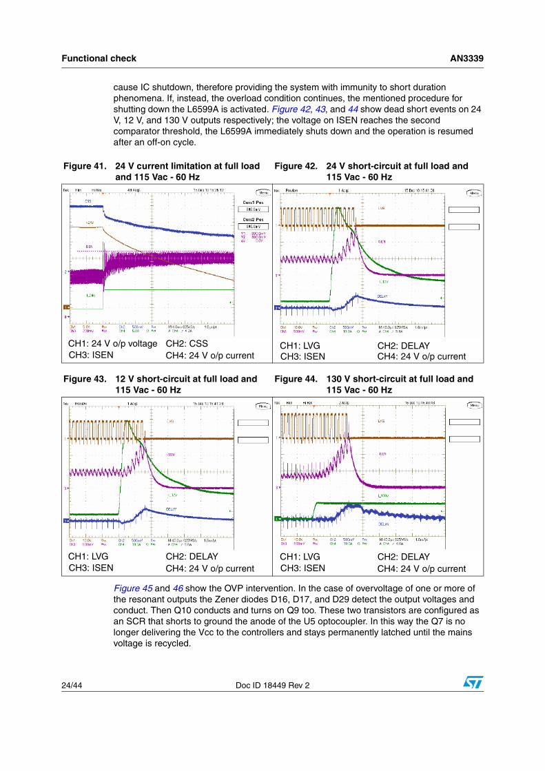
The L6599A is equipped with a current sensing input (pin #6, ISEN) and a dedicated overcurrent management system. The current flowing in the resonant tank is detected and the signal is fed into the ISEN pin. It is internally connected to a first comparator referenced to 0.8 V, and to a second comparator referenced to 1.5 V. Figure 41 shows an example of overload occurrence. If the voltage externally applied to ISEN exceeds 0.8 V, an internal switch is turned on and discharges the soft-start capacitor CSS. This operation results in a nearly constant peak primary current limiting the output power. At the same time, an internal 150 µA current generator, which, via the DELAY pin, charges C37, is activated. Because the DELAY and DIS pins short each other, if the voltage on C37 reaches 1.85 V, the L6599A stops switching and the PFC_STOP pin is pulled low disabling also the PFC.
An off-on recycle is necessary to restart the converter. By dimensioning C37 and R54, the designer can set the maximum time that the converter is allowed to run overloaded or under short-circuit conditions. Overloads or short-circuits lasting less than the set time do not
Figure 38. 12 V load transition Figure 39. 24 V load transition
CH3: +12 V CH1: +130 V CH2: +24 V
CH4: +12 V o/p current CH3: +12 VCH1: +130 V CH2: +24 V
CH4: +24 V o/p current
CH3: +12 VCH1: +130 V CH2: +24 V
CH4: +130 V o/p current
Functional check AN3339
24/44 Doc ID 18449 Rev 2
cause IC shutdown, therefore providing the system with immunity to short duration phenomena. If, instead, the overload condition continues, the mentioned procedure for shutting down the L6599A is activated. Figure 42, 43, and 44 show dead short events on 24 V, 12 V, and 130 V outputs respectively; the voltage on ISEN reaches the second comparator threshold, the L6599A immediately shuts down and the operation is resumed after an off-on cycle.
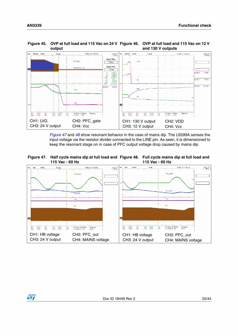
Figure 45 and 46 show the OVP intervention. In the case of overvoltage of one or more of the resonant outputs the Zener diodes D16, D17, and D29 detect the output voltages and conduct. Then Q10 conducts and turns on Q9 too. These two transistors are configured as an SCR that shorts to ground the anode of the U5 optocoupler. In this way the Q7 is no longer delivering the Vcc to the controllers and stays permanently latched until the mains voltage is recycled.
Figure 41. 24 V current limitation at full load and 115 Vac - 60 Hz
Figure 42. 24 V short-circuit at full load and 115 Vac - 60 Hz
CH3: ISEN CH1: 24 V o/p voltage CH2: CSS
CH4: 24 V o/p current CH3: ISENCH1: LVG CH2: DELAY
CH4: 24 V o/p current
Figure 43. 12 V short-circuit at full load and 115 Vac - 60 Hz
Figure 44. 130 V short-circuit at full load and 115 Vac - 60 Hz
CH3: ISEN CH1: LVG CH2: DELAY
CH4: 24 V o/p current CH3: ISENCH1: LVG CH2: DELAY
CH4: 24 V o/p current
AN3339 Functional check
Doc ID 18449 Rev 2 25/44
Figure 47 and 48 show resonant behavior in the case of mains dip. The L6599A senses the input voltage via the resistor divider connected to the LINE pin. As seen, it is dimensioned to keep the resonant stage on in case of PFC output voltage drop caused by mains dip.
Figure 45. OVP at full load and 115 Vac on 24 V output
Figure 46. OVP at full load and 115 Vac on 12 V and 130 V outputs
CH3: 24 V output CH1: LVG CH2: PFC_gate
CH4: Vcc CH3: 12 V output CH1: 130 V output CH2: VDD
CH4: Vcc
Figure 47. Half cycle mains dip at full load and 115 Vac - 60 Hz
Figure 48. Full cycle mains dip at full load and 115 Vac - 60 Hz
CH3: 24 V output CH1: HB voltage CH2: PFC_out
CH4: MAINS voltage CH3: 24 V output CH1: HB voltage CH2: PFC_out
CH4: MAINS voltage
Thermal map AN3339
26/44 Doc ID 18449 Rev 2
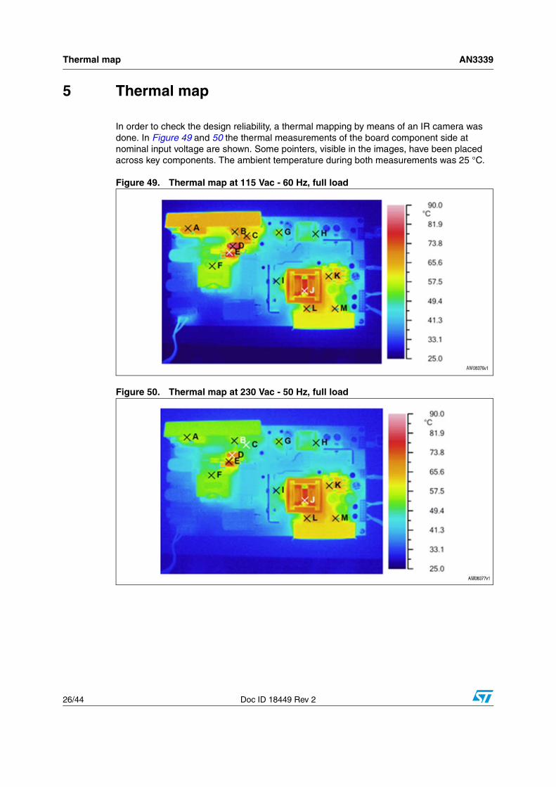
5 Thermal map
In order to check the design reliability, a thermal mapping by means of an IR camera was done. In Figure 49 and 50 the thermal measurements of the board component side at nominal input voltage are shown. Some pointers, visible in the images, have been placed across key components. The ambient temperature during both measurements was 25 °C.
Figure 49. Thermal map at 115 Vac - 60 Hz, full load
Figure 50. Thermal map at 230 Vac - 50 Hz, full load
AN3339 Thermal map
Doc ID 18449 Rev 2 27/44
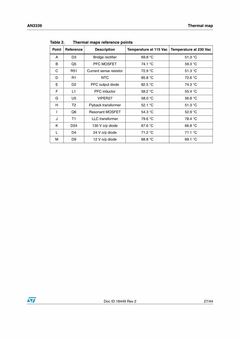
Table 2. Thermal maps reference points
Point Reference Description Temperature at 115 Vac Temperature at 230 Vac
A D3 Bridge rectifier 69.8 °C 51.3 °C
B Q5 PFC MOSFET 74.1 °C 59.3 °C
C R51 Current sense resistor 72.9 °C 51.3 °C
D R1 NTC 85.8 °C 72.6 °C
E D2 PFC output diode 82.5 °C 74.3 °C
F L1 PFC inductor 58.2 °C 55.4 °C
G U5 VIPER27 58.0 °C 56.8 °C
H T2 Flyback transformer 52.1 °C 51.3 °C
I Q6 Resonant MOSFET 54.3 °C 52.9 °C
J T1 LLC transformer 79.6 °C 78.4 °C
K D24 130 V o/p diode 67.6 °C 66.8 °C
L D4 24 V o/p diode 71.2 °C 71.1 °C
M D9 12 V o/p diode 68.8 °C 69.1 °C
Conducted emission pre-compliance test AN3339
28/44 Doc ID 18449 Rev 2
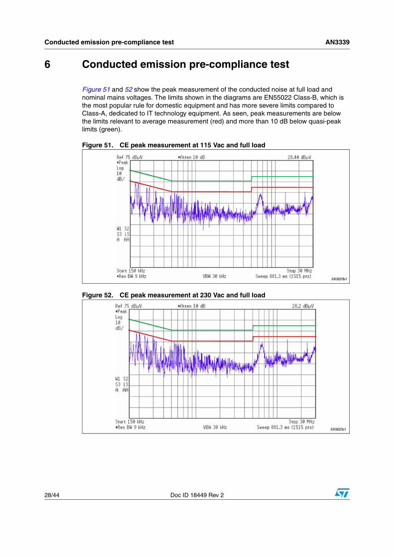
6 Conducted emission pre-compliance test
Figure 51 and 52 show the peak measurement of the conducted noise at full load and nominal mains voltages. The limits shown in the diagrams are EN55022 Class-B, which is the most popular rule for domestic equipment and has more severe limits compared to Class-A, dedicated to IT technology equipment. As seen, peak measurements are below the limits relevant to average measurement (red) and more than 10 dB below quasi-peak limits (green).
Figure 51. CE peak measurement at 115 Vac and full load
Figure 52. CE peak measurement at 230 Vac and full load
AN3339 Bill of materials
Doc ID 18449 Rev 2 29/44
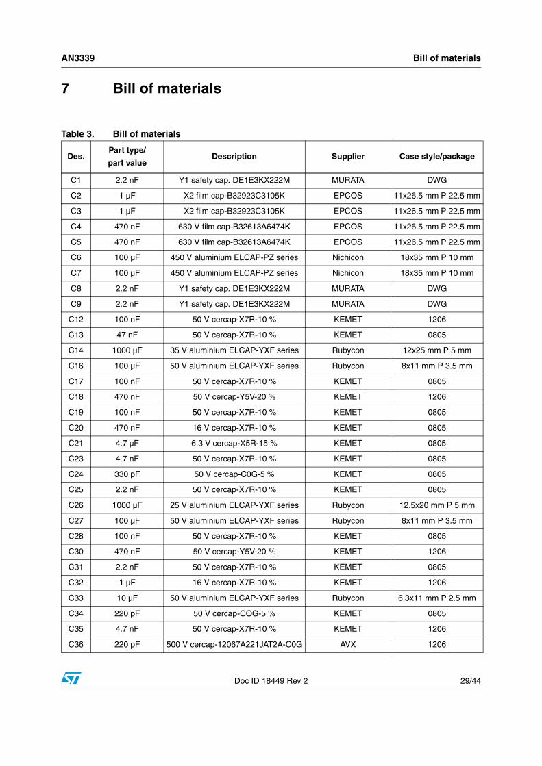
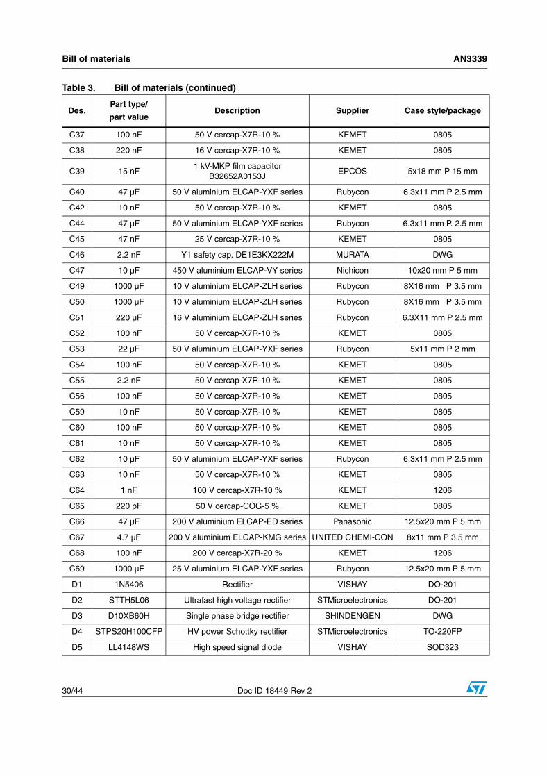
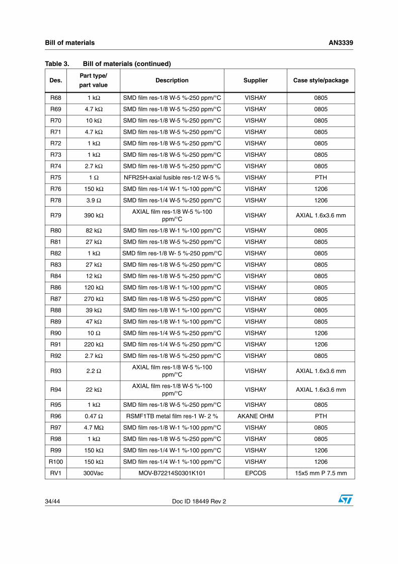
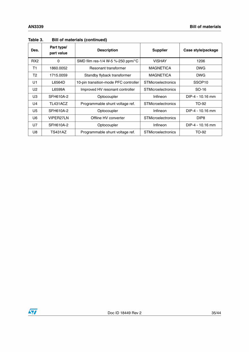
7 Bill of materials
Table 3. Bill of materials
Des.Part type/
part valueDescription Supplier Case style/package
C1 2.2 nF Y1 safety cap. DE1E3KX222M MURATA DWG
C2 1 µF X2 film cap-B32923C3105K EPCOS 11x26.5 mm P 22.5 mm
C3 1 µF X2 film cap-B32923C3105K EPCOS 11x26.5 mm P 22.5 mm
C4 470 nF 630 V film cap-B32613A6474K EPCOS 11x26.5 mm P 22.5 mm
C5 470 nF 630 V film cap-B32613A6474K EPCOS 11x26.5 mm P 22.5 mm
C6 100 µF 450 V aluminium ELCAP-PZ series Nichicon 18x35 mm P 10 mm
C7 100 µF 450 V aluminium ELCAP-PZ series Nichicon 18x35 mm P 10 mm
C8 2.2 nF Y1 safety cap. DE1E3KX222M MURATA DWG
C9 2.2 nF Y1 safety cap. DE1E3KX222M MURATA DWG
C12 100 nF 50 V cercap-X7R-10 % KEMET 1206
C13 47 nF 50 V cercap-X7R-10 % KEMET 0805
C14 1000 µF 35 V aluminium ELCAP-YXF series Rubycon 12x25 mm P 5 mm
C16 100 µF 50 V aluminium ELCAP-YXF series Rubycon 8x11 mm P 3.5 mm
C17 100 nF 50 V cercap-X7R-10 % KEMET 0805
C18 470 nF 50 V cercap-Y5V-20 % KEMET 1206
C19 100 nF 50 V cercap-X7R-10 % KEMET 0805
C20 470 nF 16 V cercap-X7R-10 % KEMET 0805
C21 4.7 µF 6.3 V cercap-X5R-15 % KEMET 0805
C23 4.7 nF 50 V cercap-X7R-10 % KEMET 0805
C24 330 pF 50 V cercap-C0G-5 % KEMET 0805
C25 2.2 nF 50 V cercap-X7R-10 % KEMET 0805
C26 1000 µF 25 V aluminium ELCAP-YXF series Rubycon 12.5x20 mm P 5 mm
C27 100 µF 50 V aluminium ELCAP-YXF series Rubycon 8x11 mm P 3.5 mm
C28 100 nF 50 V cercap-X7R-10 % KEMET 0805
C30 470 nF 50 V cercap-Y5V-20 % KEMET 1206
C31 2.2 nF 50 V cercap-X7R-10 % KEMET 0805
C32 1 µF 16 V cercap-X7R-10 % KEMET 1206
C33 10 µF 50 V aluminium ELCAP-YXF series Rubycon 6.3x11 mm P 2.5 mm
C34 220 pF 50 V cercap-COG-5 % KEMET 0805
C35 4.7 nF 50 V cercap-X7R-10 % KEMET 1206
C36 220 pF 500 V cercap-12067A221JAT2A-C0G AVX 1206
Bill of materials AN3339
30/44 Doc ID 18449 Rev 2
C37 100 nF 50 V cercap-X7R-10 % KEMET 0805
C38 220 nF 16 V cercap-X7R-10 % KEMET 0805
C39 15 nF1 kV-MKP film capacitor
B32652A0153JEPCOS 5x18 mm P 15 mm
C40 47 µF 50 V aluminium ELCAP-YXF series Rubycon 6.3x11 mm P 2.5 mm
C42 10 nF 50 V cercap-X7R-10 % KEMET 0805
C44 47 µF 50 V aluminium ELCAP-YXF series Rubycon 6.3x11 mm P. 2.5 mm
C45 47 nF 25 V cercap-X7R-10 % KEMET 0805
C46 2.2 nF Y1 safety cap. DE1E3KX222M MURATA DWG
C47 10 µF 450 V aluminium ELCAP-VY series Nichicon 10x20 mm P 5 mm
C49 1000 µF 10 V aluminium ELCAP-ZLH series Rubycon 8X16 mm P 3.5 mm
C50 1000 µF 10 V aluminium ELCAP-ZLH series Rubycon 8X16 mm P 3.5 mm
C51 220 µF 16 V aluminium ELCAP-ZLH series Rubycon 6.3X11 mm P 2.5 mm
C52 100 nF 50 V cercap-X7R-10 % KEMET 0805
C53 22 µF 50 V aluminium ELCAP-YXF series Rubycon 5x11 mm P 2 mm
C54 100 nF 50 V cercap-X7R-10 % KEMET 0805
C55 2.2 nF 50 V cercap-X7R-10 % KEMET 0805
C56 100 nF 50 V cercap-X7R-10 % KEMET 0805
C59 10 nF 50 V cercap-X7R-10 % KEMET 0805
C60 100 nF 50 V cercap-X7R-10 % KEMET 0805
C61 10 nF 50 V cercap-X7R-10 % KEMET 0805
C62 10 µF 50 V aluminium ELCAP-YXF series Rubycon 6.3x11 mm P 2.5 mm
C63 10 nF 50 V cercap-X7R-10 % KEMET 0805
C64 1 nF 100 V cercap-X7R-10 % KEMET 1206
C65 220 pF 50 V cercap-COG-5 % KEMET 0805
C66 47 µF 200 V aluminium ELCAP-ED series Panasonic 12.5x20 mm P 5 mm
C67 4.7 µF 200 V aluminium ELCAP-KMG series UNITED CHEMI-CON 8x11 mm P 3.5 mm
C68 100 nF 200 V cercap-X7R-20 % KEMET 1206
C69 1000 µF 25 V aluminium ELCAP-YXF series Rubycon 12.5x20 mm P 5 mm
D1 1N5406 Rectifier VISHAY DO-201
D2 STTH5L06 Ultrafast high voltage rectifier STMicroelectronics DO-201
D3 D10XB60H Single phase bridge rectifier SHINDENGEN DWG
D4 STPS20H100CFP HV power Schottky rectifier STMicroelectronics TO-220FP
D5 LL4148WS High speed signal diode VISHAY SOD323
Table 3. Bill of materials (continued)
Des.Part type/
part valueDescription Supplier Case style/package
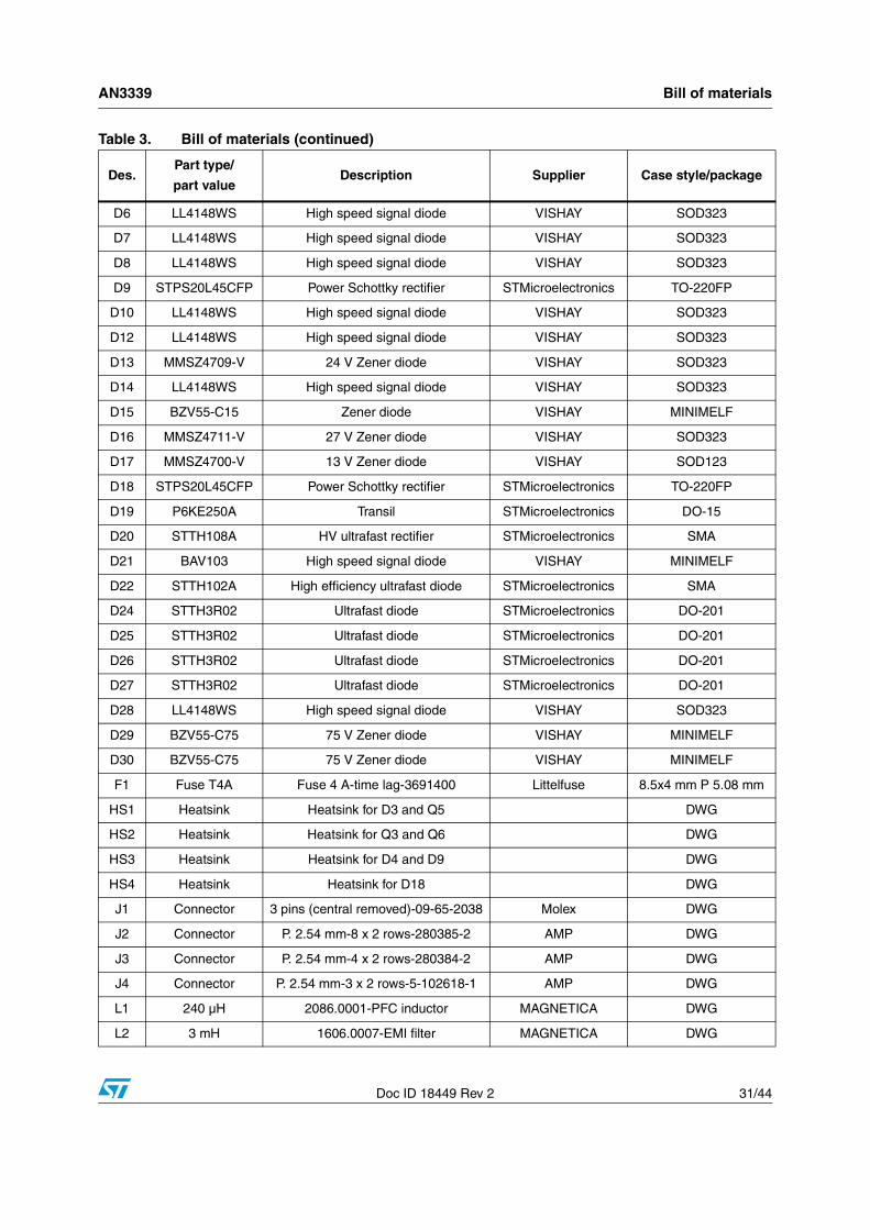
AN3339 Bill of materials
Doc ID 18449 Rev 2 31/44
D6 LL4148WS High speed signal diode VISHAY SOD323
D7 LL4148WS High speed signal diode VISHAY SOD323
D8 LL4148WS High speed signal diode VISHAY SOD323
D9 STPS20L45CFP Power Schottky rectifier STMicroelectronics TO-220FP
D10 LL4148WS High speed signal diode VISHAY SOD323
D12 LL4148WS High speed signal diode VISHAY SOD323
D13 MMSZ4709-V 24 V Zener diode VISHAY SOD323
D14 LL4148WS High speed signal diode VISHAY SOD323
D15 BZV55-C15 Zener diode VISHAY MINIMELF
D16 MMSZ4711-V 27 V Zener diode VISHAY SOD323
D17 MMSZ4700-V 13 V Zener diode VISHAY SOD123
D18 STPS20L45CFP Power Schottky rectifier STMicroelectronics TO-220FP
D19 P6KE250A Transil STMicroelectronics DO-15
D20 STTH108A HV ultrafast rectifier STMicroelectronics SMA
D21 BAV103 High speed signal diode VISHAY MINIMELF
D22 STTH102A High efficiency ultrafast diode STMicroelectronics SMA
D24 STTH3R02 Ultrafast diode STMicroelectronics DO-201
D25 STTH3R02 Ultrafast diode STMicroelectronics DO-201
D26 STTH3R02 Ultrafast diode STMicroelectronics DO-201
D27 STTH3R02 Ultrafast diode STMicroelectronics DO-201
D28 LL4148WS High speed signal diode VISHAY SOD323
D29 BZV55-C75 75 V Zener diode VISHAY MINIMELF
D30 BZV55-C75 75 V Zener diode VISHAY MINIMELF
F1 Fuse T4A Fuse 4 A-time lag-3691400 Littelfuse 8.5x4 mm P 5.08 mm
HS1 Heatsink Heatsink for D3 and Q5 DWG
HS2 Heatsink Heatsink for Q3 and Q6 DWG
HS3 Heatsink Heatsink for D4 and D9 DWG
HS4 Heatsink Heatsink for D18 DWG
J1 Connector 3 pins (central removed)-09-65-2038 Molex DWG
J2 Connector P. 2.54 mm-8 x 2 rows-280385-2 AMP DWG
J3 Connector P. 2.54 mm-4 x 2 rows-280384-2 AMP DWG
J4 Connector P. 2.54 mm-3 x 2 rows-5-102618-1 AMP DWG
L1 240 µH 2086.0001-PFC inductor MAGNETICA DWG
L2 3 mH 1606.0007-EMI filter MAGNETICA DWG
Table 3. Bill of materials (continued)
Des.Part type/
part valueDescription Supplier Case style/package
Bill of materials AN3339
32/44 Doc ID 18449 Rev 2
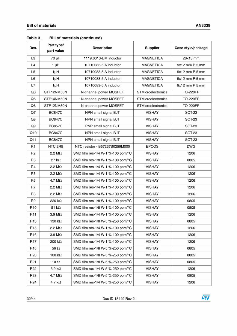
L3 70 µH 1119.0013-DM inductor MAGNETICA 26x13 mm
L4 1 µH 10710083-5 A inductor MAGNETICA 9x12 mm P 5 mm
L5 1µH 10710083-5 A inductor MAGNETICA 9x12 mm P 5 mm
L6 1µH 10710083-5 A inductor MAGNETICA 9x12 mm P 5 mm
L7 1µH 10710083-5 A inductor MAGNETICA 9x12 mm P 5 mm
Q3 STF12NM50N N-channel power MOSFET STMicroelectronics TO-220FP
Q5 STF14NM50N N-channel power MOSFET STMicroelectronics TO-220FP
Q6 STF12NM50N N-channel power MOSFET STMicroelectronics TO-220FP
Q7 BC847C NPN small signal BJT VISHAY SOT-23
Q8 BC847C NPN small signal BJT VISHAY SOT-23
Q9 BC857C PNP small signal BJT VISHAY SOT-23
Q10 BC847C NPN small signal BJT VISHAY SOT-23
Q11 BC847C NPN small signal BJT VISHAY SOT-23
R1 NTC 2R5 NTC resistor - B57237S0259M000 EPCOS DWG
R2 2.2 MΩ SMD film res-1/4 W-1 %-100 ppm/°C VISHAY 1206
R3 27 kΩ SMD film res-1/8 W-1 %-100 ppm/°C VISHAY 0805
R4 2.2 MΩ SMD film res-1/4 W-1 %-100 ppm/°C VISHAY 1206
R5 2.2 MΩ SMD film res-1/4 W-1 %-100 ppm/°C VISHAY 1206
R6 4.7 MΩ SMD film res-1/4 W-1 %-100 ppm/°C VISHAY 1206
R7 2.2 MΩ SMD film res-1/4 W-1 %-100 ppm/°C VISHAY 1206
R8 2.2 MΩ SMD film res-1/4 W-1 %-100 ppm/°C VISHAY 1206
R9 220 kΩ SMD film res-1/8 W-1 %-100 ppm/°C VISHAY 0805
R10 51 kΩ SMD film res-1/8 W-1 %-100 ppm/°C VISHAY 0805
R11 3.9 MΩ SMD film res-1/4 W-1 %-100 ppm/°C VISHAY 1206
R13 130 kΩ SMD film res-1/8 W-5 %-250 ppm/°C VISHAY 0805
R15 2.2 MΩ SMD film res-1/4 W-1 %-100 ppm/°C VISHAY 1206
R16 3.9 MΩ SMD film res-1/4 W-1 %-100 ppm/°C VISHAY 1206
R17 200 kΩ SMD film res-1/4 W-1 %-100 ppm/°C VISHAY 1206
R18 56 Ω SMD film res-1/8 W-5 %-250 ppm/°C VISHAY 0805
R20 100 kΩ SMD film res-1/8 W-5 %-250 ppm/°C VISHAY 0805
R21 10 Ω SMD film res-1/8 W-5 %-250 ppm/°C VISHAY 0805
R22 3.9 kΩ SMD film res-1/4 W-5 %-250 ppm/°C VISHAY 1206
R23 4.7 MΩ SMD film res-1/8 W-5 %-250 ppm/°C VISHAY 0805
R24 4.7 kΩ SMD film res-1/4 W-5 %-250 ppm/°C VISHAY 1206
Table 3. Bill of materials (continued)
Des.Part type/
part valueDescription Supplier Case style/package
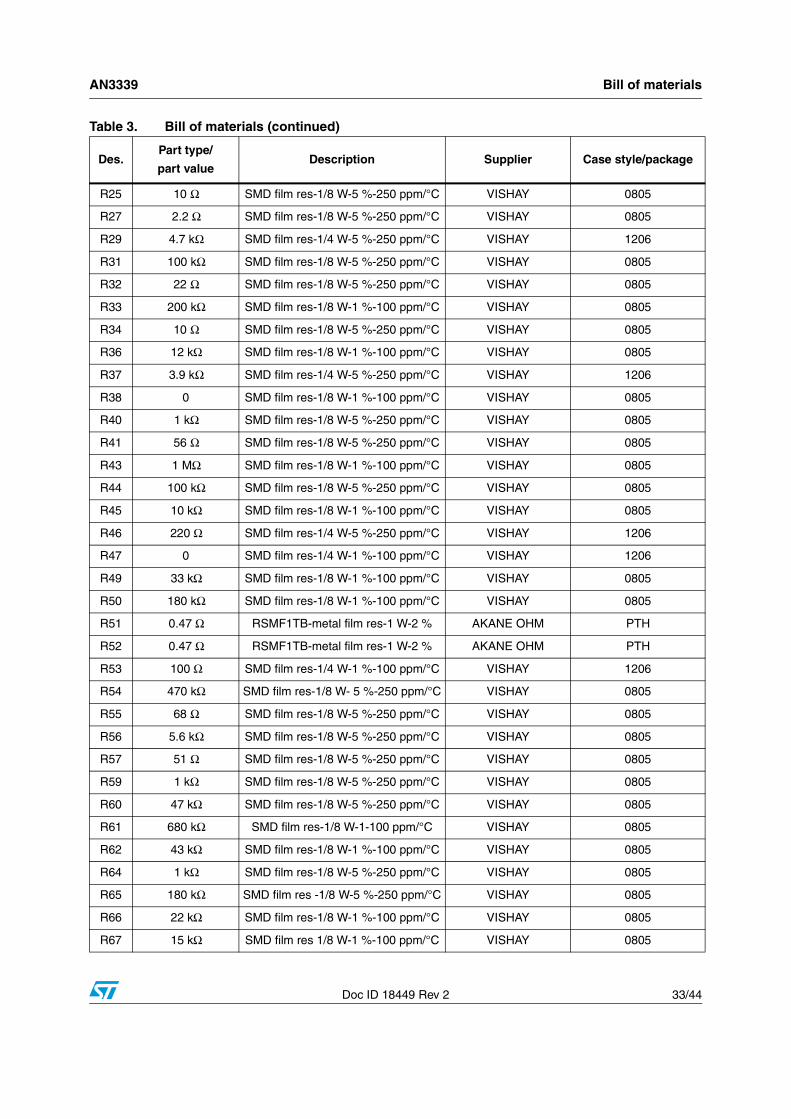
AN3339 Bill of materials
Doc ID 18449 Rev 2 33/44
R25 10 Ω SMD film res-1/8 W-5 %-250 ppm/°C VISHAY 0805
R27 2.2 Ω SMD film res-1/8 W-5 %-250 ppm/°C VISHAY 0805
R29 4.7 kΩ SMD film res-1/4 W-5 %-250 ppm/°C VISHAY 1206
R31 100 kΩ SMD film res-1/8 W-5 %-250 ppm/°C VISHAY 0805
R32 22 Ω SMD film res-1/8 W-5 %-250 ppm/°C VISHAY 0805
R33 200 kΩ SMD film res-1/8 W-1 %-100 ppm/°C VISHAY 0805
R34 10 Ω SMD film res-1/8 W-5 %-250 ppm/°C VISHAY 0805
R36 12 kΩ SMD film res-1/8 W-1 %-100 ppm/°C VISHAY 0805
R37 3.9 kΩ SMD film res-1/4 W-5 %-250 ppm/°C VISHAY 1206
R38 0 SMD film res-1/8 W-1 %-100 ppm/°C VISHAY 0805
R40 1 kΩ SMD film res-1/8 W-5 %-250 ppm/°C VISHAY 0805
R41 56 Ω SMD film res-1/8 W-5 %-250 ppm/°C VISHAY 0805
R43 1 MΩ SMD film res-1/8 W-1 %-100 ppm/°C VISHAY 0805
R44 100 kΩ SMD film res-1/8 W-5 %-250 ppm/°C VISHAY 0805
R45 10 kΩ SMD film res-1/8 W-1 %-100 ppm/°C VISHAY 0805
R46 220 Ω SMD film res-1/4 W-5 %-250 ppm/°C VISHAY 1206
R47 0 SMD film res-1/4 W-1 %-100 ppm/°C VISHAY 1206
R49 33 kΩ SMD film res-1/8 W-1 %-100 ppm/°C VISHAY 0805
R50 180 kΩ SMD film res-1/8 W-1 %-100 ppm/°C VISHAY 0805
R51 0.47 Ω RSMF1TB-metal film res-1 W-2 % AKANE OHM PTH
R52 0.47 Ω RSMF1TB-metal film res-1 W-2 % AKANE OHM PTH
R53 100 Ω SMD film res-1/4 W-1 %-100 ppm/°C VISHAY 1206
R54 470 kΩ SMD film res-1/8 W- 5 %-250 ppm/°C VISHAY 0805
R55 68 Ω SMD film res-1/8 W-5 %-250 ppm/°C VISHAY 0805
R56 5.6 kΩ SMD film res-1/8 W-5 %-250 ppm/°C VISHAY 0805
R57 51 Ω SMD film res-1/8 W-5 %-250 ppm/°C VISHAY 0805
R59 1 kΩ SMD film res-1/8 W-5 %-250 ppm/°C VISHAY 0805
R60 47 kΩ SMD film res-1/8 W-5 %-250 ppm/°C VISHAY 0805
R61 680 kΩ SMD film res-1/8 W-1-100 ppm/°C VISHAY 0805
R62 43 kΩ SMD film res-1/8 W-1 %-100 ppm/°C VISHAY 0805
R64 1 kΩ SMD film res-1/8 W-5 %-250 ppm/°C VISHAY 0805
R65 180 kΩ SMD film res -1/8 W-5 %-250 ppm/°C VISHAY 0805
R66 22 kΩ SMD film res-1/8 W-1 %-100 ppm/°C VISHAY 0805
R67 15 kΩ SMD film res 1/8 W-1 %-100 ppm/°C VISHAY 0805
Table 3. Bill of materials (continued)
Des.Part type/
part valueDescription Supplier Case style/package
Bill of materials AN3339
34/44 Doc ID 18449 Rev 2
R68 1 kΩ SMD film res-1/8 W-5 %-250 ppm/°C VISHAY 0805
R69 4.7 kΩ SMD film res-1/8 W-5 %-250 ppm/°C VISHAY 0805
R70 10 kΩ SMD film res-1/8 W-5 %-250 ppm/°C VISHAY 0805
R71 4.7 kΩ SMD film res-1/8 W-5 %-250 ppm/°C VISHAY 0805
R72 1 kΩ SMD film res-1/8 W-5 %-250 ppm/°C VISHAY 0805
R73 1 kΩ SMD film res-1/8 W-5 %-250 ppm/°C VISHAY 0805
R74 2.7 kΩ SMD film res-1/8 W-5 %-250 ppm/°C VISHAY 0805
R75 1 Ω NFR25H-axial fusible res-1/2 W-5 % VISHAY PTH
R76 150 kΩ SMD film res-1/4 W-1 %-100 ppm/°C VISHAY 1206
R78 3.9 Ω SMD film res-1/4 W-5 %-250 ppm/°C VISHAY 1206
R79 390 kΩ AXIAL film res-1/8 W-5 %-100 ppm/°C
VISHAY AXIAL 1.6x3.6 mm
R80 82 kΩ SMD film res-1/8 W-1 %-100 ppm/°C VISHAY 0805
R81 27 kΩ SMD film res-1/8 W-5 %-250 ppm/°C VISHAY 0805
R82 1 kΩ SMD film res-1/8 W- 5 %-250 ppm/°C VISHAY 0805
R83 27 kΩ SMD film res-1/8 W-5 %-250 ppm/°C VISHAY 0805
R84 12 kΩ SMD film res-1/8 W-5 %-250 ppm/°C VISHAY 0805
R86 120 kΩ SMD film res-1/8 W-1 %-100 ppm/°C VISHAY 0805
R87 270 kΩ SMD film res-1/8 W-5 %-250 ppm/°C VISHAY 0805
R88 39 kΩ SMD film res-1/8 W-1 %-100 ppm/°C VISHAY 0805
R89 47 kΩ SMD film res-1/8 W-1 %-100 ppm/°C VISHAY 0805
R90 10 Ω SMD film res-1/4 W-5 %-250 ppm/°C VISHAY 1206
R91 220 kΩ SMD film res-1/4 W-5 %-250 ppm/°C VISHAY 1206
R92 2.7 kΩ SMD film res-1/8 W-5 %-250 ppm/°C VISHAY 0805
R93 2.2 Ω AXIAL film res-1/8 W-5 %-100 ppm/°C
VISHAY AXIAL 1.6x3.6 mm
R94 22 kΩ AXIAL film res-1/8 W-5 %-100 ppm/°C
VISHAY AXIAL 1.6x3.6 mm
R95 1 kΩ SMD film res-1/8 W-5 %-250 ppm/°C VISHAY 0805
R96 0.47 Ω RSMF1TB metal film res-1 W- 2 % AKANE OHM PTH
R97 4.7 MΩ SMD film res-1/8 W-1 %-100 ppm/°C VISHAY 0805
R98 1 kΩ SMD film res-1/8 W-5 %-250 ppm/°C VISHAY 0805
R99 150 kΩ SMD film res-1/4 W-1 %-100 ppm/°C VISHAY 1206
R100 150 kΩ SMD film res-1/4 W-1 %-100 ppm/°C VISHAY 1206
RV1 300Vac MOV-B72214S0301K101 EPCOS 15x5 mm P 7.5 mm
Table 3. Bill of materials (continued)
Des.Part type/
part valueDescription Supplier Case style/package
AN3339 Bill of materials
Doc ID 18449 Rev 2 35/44
RX2 0 SMD film res-1/4 W-5 %-250 ppm/°C VISHAY 1206
T1 1860.0052 Resonant transformer MAGNETICA DWG
T2 1715.0059 Standby flyback transformer MAGNETICA DWG
U1 L6564D 10-pin transition-mode PFC controller STMicroelectronics SSOP10
U2 L6599A Improved HV resonant controller STMicroelectronics SO-16
U3 SFH610A-2 Optocoupler Infineon DIP-4 - 10.16 mm
U4 TL431ACZ Programmable shunt voltage ref. STMicroelectronics TO-92
U5 SFH610A-2 Optocoupler Infineon DIP-4 - 10.16 mm
U6 VIPER27LN Offline HV converter STMicroelectronics DIP8
U7 SFH610A-2 Optocoupler Infineon DIP-4 - 10.16 mm
U8 TS431AZ Programmable shunt voltage ref. STMicroelectronics TO-92
Table 3. Bill of materials (continued)
Des.Part type/
part valueDescription Supplier Case style/package
PFC coil specification AN3339
36/44 Doc ID 18449 Rev 2
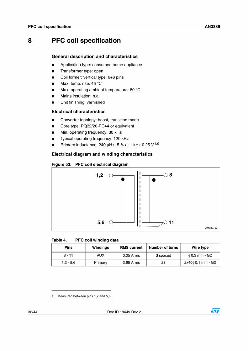
8 PFC coil specification
General description and characteristics
● Application type: consumer, home appliance
● Transformer type: open
● Coil former: vertical type, 6+6 pins
● Max. temp. rise: 45 °C
● Max. operating ambient temperature: 60 °C
● Mains insulation: n.a
● Unit finishing: varnished
Electrical characteristics
● Converter topology: boost, transition mode
● Core type: PQ32/20-PC44 or equivalent
● Min. operating frequency: 30 kHz
● Typical operating frequency: 120 kHz
● Primary inductance: 240 µH±15 % at 1 kHz-0.25 V (a)
Electrical diagram and winding characteristics
Figure 53. PFC coil electrical diagram
a. Measured between pins 1,2 and 5,6.
Table 4. PFC coil winding data
Pins Windings RMS current Number of turns Wire type
8 - 11 AUX 0.05 Arms 3 spaced φ 0.3 mm - G2
1,2 - 5,6 Primary 2.65 Arms 28 2x40φ 0.1 mm - G2
AN3339 PFC coil specification
Doc ID 18449 Rev 2 37/44
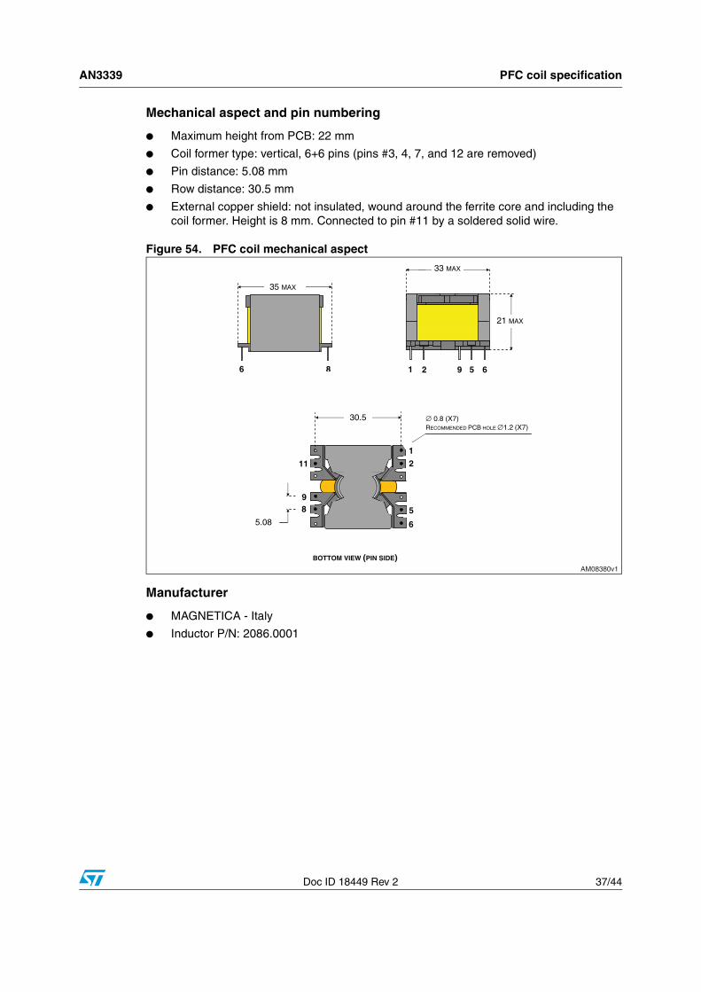
Mechanical aspect and pin numbering
● Maximum height from PCB: 22 mm
● Coil former type: vertical, 6+6 pins (pins #3, 4, 7, and 12 are removed)
● Pin distance: 5.08 mm
● Row distance: 30.5 mm
● External copper shield: not insulated, wound around the ferrite core and including the coil former. Height is 8 mm. Connected to pin #11 by a soldered solid wire.
Figure 54. PFC coil mechanical aspect
Manufacturer
● MAGNETICA - Italy
● Inductor P/N: 2086.0001
AM08380v1
BOTTOM VIEW (PIN SIDE)
∅ 0.8 (X7) RECOMMENDED PCB HOLE ∅1.2 (X7)
35 MAX
6 8 1 2 9 5 6
33 MAX
21 MAX
1
2
5
6
11
9 8
5.08
30.5
Resonant power transformer specification AN3339
38/44 Doc ID 18449 Rev 2
9 Resonant power transformer specification
General description and characteristics
● Application type: consumer, home appliance
● Transformer type: open
● Coil former: horizontal type, 7+7 pins, two slots
● Max. temp. rise: 45 °C
● Max. operating ambient temperature: 60 °C
● Mains insulation: acc. to EN60065
Electrical characteristics
● Converter topology: half bridge, resonant
● Core type: ETD34-PC44 or equivalent
● Min. operating frequency: 60 kHz
● Typical operating frequency: 110 kHz
● Primary inductance: 620 µH±10 % at 1 kHz-0.25 V(b)
● Leakage inductance: 105 µH at 100 kHz-0.25 V(c)
Electrical diagram and winding characteristics
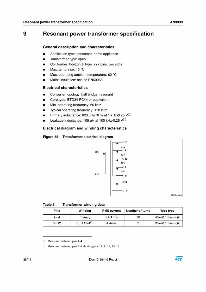
Figure 55. Transformer electrical diagram
b. Measured between pins 2-4.
c. Measured between pins 2-4 shorting pins 12, 9, 11, 13, 14.
Table 5. Transformer winding data
Pins Winding RMS current Number of turns Wire type
2 - 4 Primary 1.2 Arms 36 40xφ 0.1 mm - G2
8 - 12 SEC 12-A(1) 4 Arms 2 90xφ 0.1 mm - G2
AN3339 Resonant power transformer specification
Doc ID 18449 Rev 2 39/44
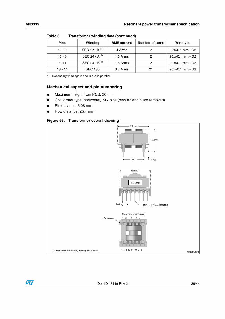
Mechanical aspect and pin numbering
● Maximum height from PCB: 30 mm
● Coil former type: horizontal, 7+7 pins (pins #3 and 5 are removed)
● Pin distance: 5.08 mm
● Row distance: 25.4 mm
Figure 56. Transformer overall drawing
12 - 9 SEC 12 - B (1) 4 Arms 2 90xφ 0.1 mm - G2
10 - 8 SEC 24 - A(1) 1.6 Arms 2 90xφ 0.1 mm - G2
9 - 11 SEC 24 - B(1) 1.6 Arms 2 90xφ 0.1 mm - G2
13 - 14 SEC 130 0.7 Arms 21 90xφ 0.1 mm - G2
1. Secondary windings A and B are in parallel.
Table 5. Transformer winding data (continued)
Pins Winding RMS current Number of turns Wire type

Resonant power transformer specification AN3339
40/44 Doc ID 18449 Rev 2
Manufacturer
● MAGNETICA - Italy
● Transformer P/N: 1860.0052
AN3339 Flyback transformer specification
Doc ID 18449 Rev 2 41/44
10 Flyback transformer specification
General description and characteristics
● Application type: consumer, home appliance
● Transformer type: open
● Coil former: horizontal type, 5+4 pins
● Max. temp. rise: 45 °C
● Max. operating ambient temperature: 60 °C
● Mains insulation: acc. to EN60065
Electrical characteristics
● Converter topology: fixed frequency flyback
● Core type: E20-PC44 or equivalent
● Typical operating frequency: 60 kHz
● Primary inductance: 2.38 mH±15 % at 1 kHz-0.25 V(d)
● Leakage inductance: <30 µH at 100 kHz-0.25 V(e)
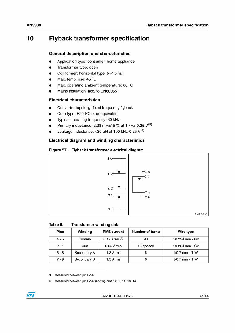
Electrical diagram and winding characteristics
Figure 57. Flyback transformer electrical diagram
d. Measured between pins 2-4.
e. Measured between pins 2-4 shorting pins 12, 9, 11, 13, 14.
Table 6. Transformer winding data
Pins Winding RMS current Number of turns Wire type
4 - 5 Primary 0.17 Arms(1) 93 φ 0.224 mm - G2
2 - 1 Aux 0.05 Arms 18 spaced φ 0.224 mm - G2
6 - 8 Secondary A 1.3 Arms 6 φ 0.7 mm - TIW
7 - 9 Secondary B 1.3 Arms 6 φ 0.7 mm - TIW
Flyback transformer specification AN3339
42/44 Doc ID 18449 Rev 2
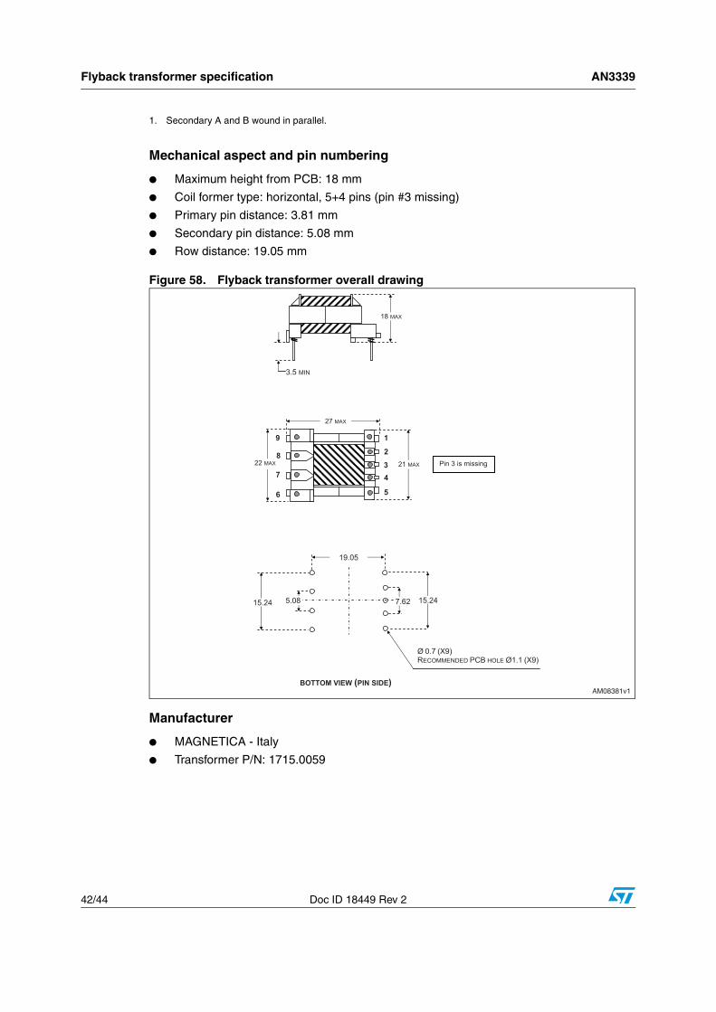
Mechanical aspect and pin numbering
● Maximum height from PCB: 18 mm
● Coil former type: horizontal, 5+4 pins (pin #3 missing)
● Primary pin distance: 3.81 mm
● Secondary pin distance: 5.08 mm
● Row distance: 19.05 mm
Figure 58. Flyback transformer overall drawing
Manufacturer
● MAGNETICA - Italy
● Transformer P/N: 1715.0059
1. Secondary A and B wound in parallel.
AM08381v1
Ø 0.7 (X9) RECOMMENDED PCB HOLE Ø1.1 (X9)
3.5 MIN
18 MAX
1
2
43
5
9
8
6
7
27 MAX
21 MAX
7.625.08 15.24
19.05
15.24
22 MAX
BOTTOM VIEW (PIN SIDE)
Pin 3 is missing

AN3339 Revision history
Doc ID 18449 Rev 2 43/44
11 Revision history
Table 7. Document revision history
Date Revision Changes
23-Feb-2011 1 Initial release.
30-Aug-2012 2 Minor text changes to improve readability, no technical changes.

AN3339
44/44 Doc ID 18449 Rev 2
Please Read Carefully:
Information in this document is provided solely in connection with ST products. STMicroelectronics NV and its subsidiaries (“ST”) reserve theright to make changes, corrections, modifications or improvements, to this document, and the products and services described herein at anytime, without notice.
All ST products are sold pursuant to ST’s terms and conditions of sale.
Purchasers are solely responsible for the choice, selection and use of the ST products and services described herein, and ST assumes noliability whatsoever relating to the choice, selection or use of the ST products and services described herein.
No license, express or implied, by estoppel or otherwise, to any intellectual property rights is granted under this document. If any part of thisdocument refers to any third party products or services it shall not be deemed a license grant by ST for the use of such third party productsor services, or any intellectual property contained therein or considered as a warranty covering the use in any manner whatsoever of suchthird party products or services or any intellectual property contained therein.
UNLESS OTHERWISE SET FORTH IN ST’S TERMS AND CONDITIONS OF SALE ST DISCLAIMS ANY EXPRESS OR IMPLIEDWARRANTY WITH RESPECT TO THE USE AND/OR SALE OF ST PRODUCTS INCLUDING WITHOUT LIMITATION IMPLIEDWARRANTIES OF MERCHANTABILITY, FITNESS FOR A PARTICULAR PURPOSE (AND THEIR EQUIVALENTS UNDER THE LAWSOF ANY JURISDICTION), OR INFRINGEMENT OF ANY PATENT, COPYRIGHT OR OTHER INTELLECTUAL PROPERTY RIGHT.
UNLESS EXPRESSLY APPROVED IN WRITING BY TWO AUTHORIZED ST REPRESENTATIVES, ST PRODUCTS ARE NOTRECOMMENDED, AUTHORIZED OR WARRANTED FOR USE IN MILITARY, AIR CRAFT, SPACE, LIFE SAVING, OR LIFE SUSTAININGAPPLICATIONS, NOR IN PRODUCTS OR SYSTEMS WHERE FAILURE OR MALFUNCTION MAY RESULT IN PERSONAL INJURY,DEATH, OR SEVERE PROPERTY OR ENVIRONMENTAL DAMAGE. ST PRODUCTS WHICH ARE NOT SPECIFIED AS "AUTOMOTIVEGRADE" MAY ONLY BE USED IN AUTOMOTIVE APPLICATIONS AT USER’S OWN RISK.
Resale of ST products with provisions different from the statements and/or technical features set forth in this document shall immediately voidany warranty granted by ST for the ST product or service described herein and shall not create or extend in any manner whatsoever, anyliability of ST.
ST and the ST logo are trademarks or registered trademarks of ST in various countries.
Information in this document supersedes and replaces all information previously supplied.
The ST logo is a registered trademark of STMicroelectronics. All other names are the property of their respective owners.
© 2012 STMicroelectronics - All rights reserved
STMicroelectronics group of companies
Australia - Belgium - Brazil - Canada - China - Czech Republic - Finland - France - Germany - Hong Kong - India - Israel - Italy - Japan - Malaysia - Malta - Morocco - Philippines - Singapore - Spain - Sweden - Switzerland - United Kingdom - United States of America
www.st.com