Embed Size (px)
Citation preview
Nano-Bio Electronic Materials and processing Lab.SPCC 2018 Boston
April 11, 2018
Jung-Hwan Lee1, Murhukrishnan Purushothaman1, Kwang-Min Han1,
Shohei Shima3, Satomi Hamada3, Hirokuni Hiyama3, and Jin-Goo Park1,2,*
Department of 1Bionanotechnology and 2Materials Science and Chemical Engineering, Hanyang University,
3EBARA Corporation *[email protected]
19th Surface Preparation and Cleaning Conference (SPCC)
2Nano-Bio Electronic Materials and Processing Lab.
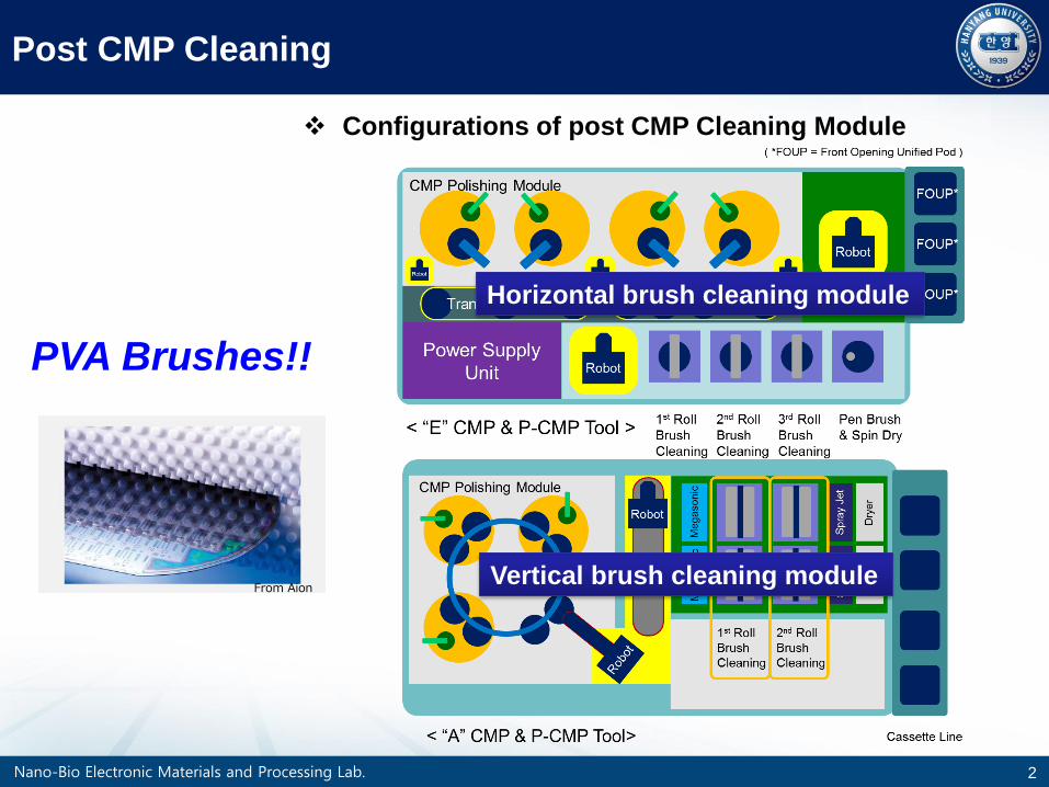
Post CMP Cleaning
PVA Brushes!!
From Aion
Horizontal brush cleaning module
Vertical brush cleaning module
Configurations of post CMP Cleaning Module
3Nano-Bio Electronic Materials and Processing Lab.
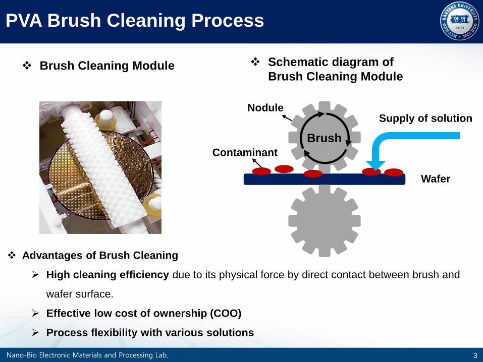
Advantages of Brush Cleaning
High cleaning efficiency due to its physical force by direct contact between brush and
wafer surface.
Effective low cost of ownership (COO)
Process flexibility with various solutions
PVA Brush Cleaning Process
Wafer
BrushContaminant
NoduleSupply of solution
Brush Cleaning Module Schematic diagram of
Brush Cleaning Module
4Nano-Bio Electronic Materials and Processing Lab.
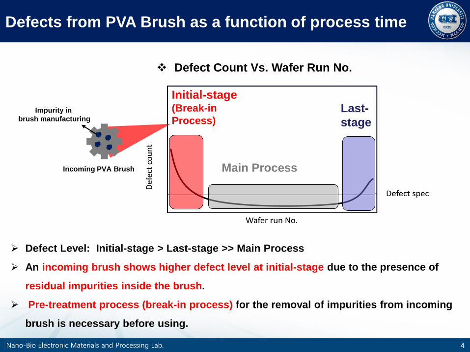
Defects from PVA Brush as a function of process time
Initial-stage(Break-in
Process)Last-
stage
Main Process
Defect Count Vs. Wafer Run No.
Defect Level: Initial-stage > Last-stage >> Main Process
An incoming brush shows higher defect level at initial-stage due to the presence of
residual impurities inside the brush.
Pre-treatment process (break-in process) for the removal of impurities from incoming
brush is necessary before using.
Impurity in
brush manufacturing
Incoming PVA Brush
5Nano-Bio Electronic Materials and Processing Lab.
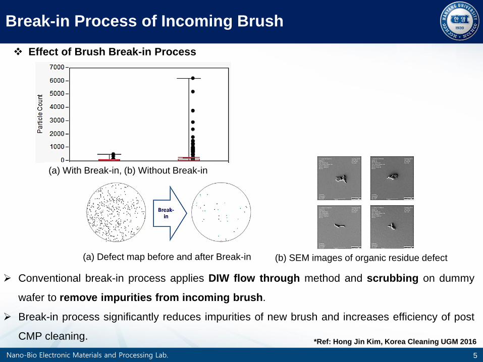
Effect of Brush Break-in Process
Conventional break-in process applies DIW flow through method and scrubbing on dummy
wafer to remove impurities from incoming brush.
Break-in process significantly reduces impurities of new brush and increases efficiency of post
CMP cleaning.
Break-in Process of Incoming Brush
*Ref: Hong Jin Kim, Korea Cleaning UGM 2016
(a) With Break-in, (b) Without Break-in
(a) Defect map before and after Break-in (b) SEM images of organic residue defect
6Nano-Bio Electronic Materials and Processing Lab.
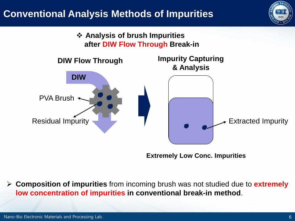
Conventional Analysis Methods of Impurities
DIW
Analysis of brush Impurities
after DIW Flow Through Break-in
Extremely Low Conc. Impurities
DIW Flow Through Impurity Capturing
& Analysis
Composition of impurities from incoming brush was not studied due to extremely
low concentration of impurities in conventional break-in method.
PVA Brush
Residual Impurity Extracted Impurity
7Nano-Bio Electronic Materials and Processing Lab.
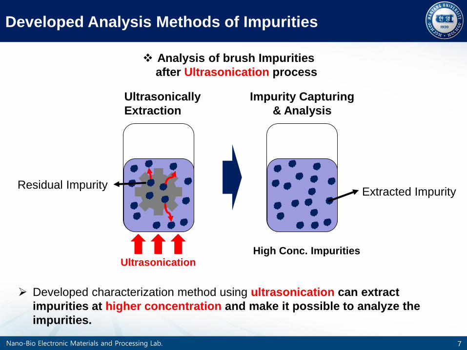
Developed Analysis Methods of Impurities
Analysis of brush Impurities
after Ultrasonication process
Ultrasonically
Extraction
Impurity Capturing
& Analysis
High Conc. Impurities
Developed characterization method using ultrasonication can extract
impurities at higher concentration and make it possible to analyze the
impurities.
Ultrasonication
Residual ImpurityExtracted Impurity
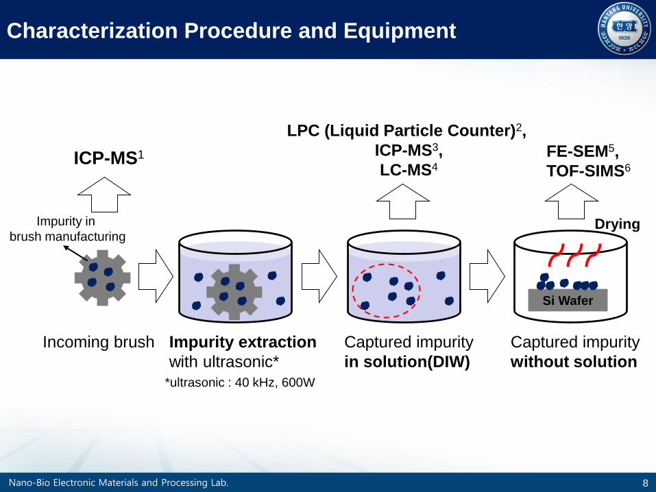
8Nano-Bio Electronic Materials and Processing Lab.
Si Wafer
Incoming brush Impurity extraction
with ultrasonic*
Captured impurity
in solution(DIW)
Captured impurity
without solution
DryingImpurity in
brush manufacturing
ICP-MS1
*ultrasonic : 40 kHz, 600W
LPC (Liquid Particle Counter)2,
ICP-MS3,
LC-MS4
FE-SEM5,
TOF-SIMS6
Characterization Procedure and Equipment
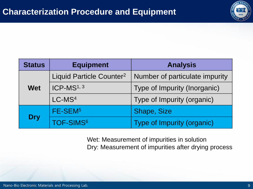
9Nano-Bio Electronic Materials and Processing Lab.
Status Equipment Analysis
Wet
Liquid Particle Counter2 Number of particulate impurity
ICP-MS1, 3 Type of Impurity (Inorganic)
LC-MS4 Type of Impurity (organic)
DryFE-SEM5 Shape, Size
TOF-SIMS6 Type of Impurity (organic)
Characterization Procedure and Equipment
Wet: Measurement of impurities in solution
Dry: Measurement of impurities after drying process
10Nano-Bio Electronic Materials and Processing Lab.
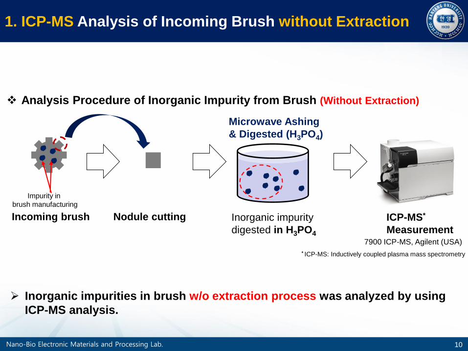
Incoming brush
Microwave Ashing
& Digested (H3PO4)
Inorganic impurity
digested in H3PO4
Nodule cutting ICP-MS*
Measurement
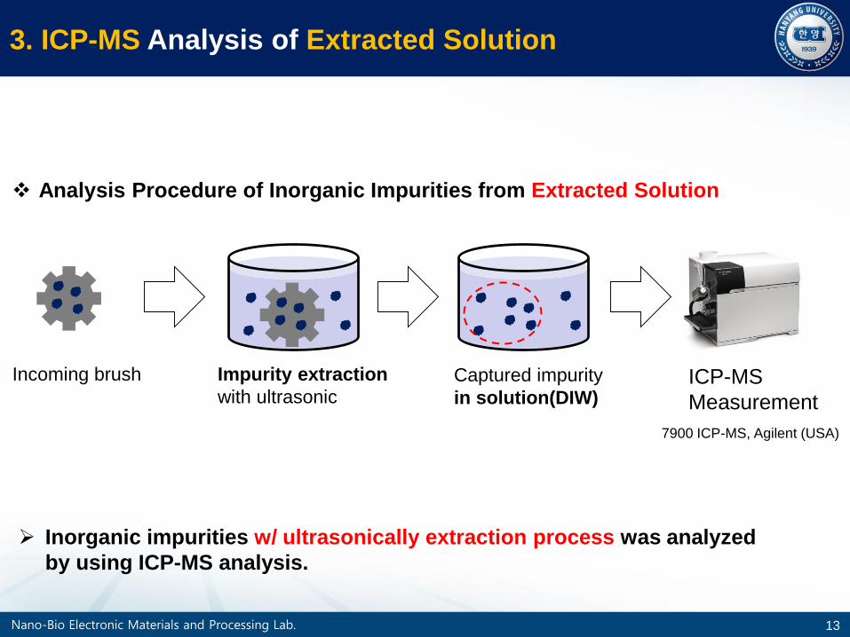
Analysis Procedure of Inorganic Impurity from Brush (Without Extraction)
7900 ICP-MS, Agilent (USA)
Inorganic impurities in brush w/o extraction process was analyzed by using
ICP-MS analysis.
1. ICP-MS Analysis of Incoming Brush without Extraction
Impurity in
brush manufacturing
* ICP-MS: Inductively coupled plasma mass spectrometry
11Nano-Bio Electronic Materials and Processing Lab.
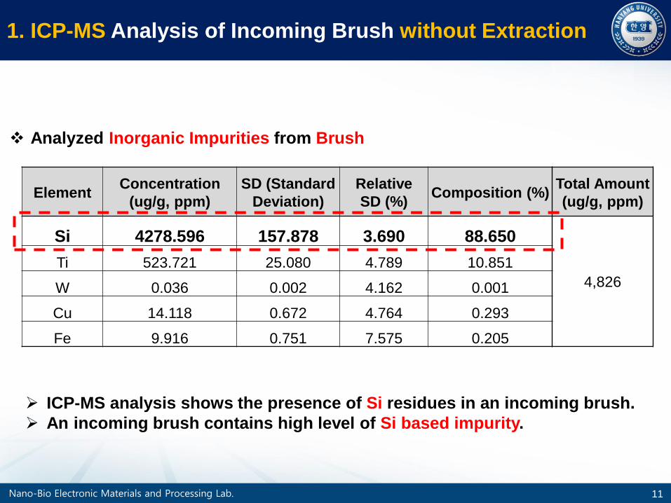
ElementConcentration
(ug/g, ppm)
SD (Standard
Deviation)
Relative
SD (%)Composition (%)
Total Amount
(ug/g, ppm)
Si 4278.596 157.878 3.690 88.650
4,826
Ti 523.721 25.080 4.789 10.851
W 0.036 0.002 4.162 0.001
Cu 14.118 0.672 4.764 0.293
Fe 9.916 0.751 7.575 0.205
Analyzed Inorganic Impurities from Brush
ICP-MS analysis shows the presence of Si residues in an incoming brush.
An incoming brush contains high level of Si based impurity.
1. ICP-MS Analysis of Incoming Brush without Extraction
12Nano-Bio Electronic Materials and Processing Lab.
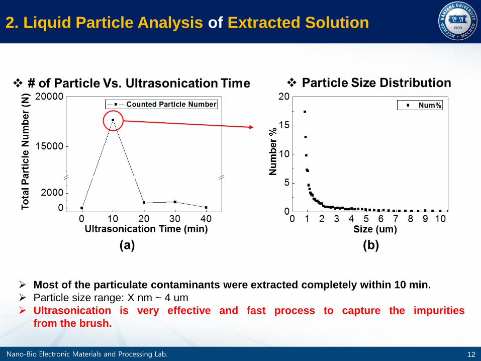
2. Liquid Particle Analysis of Extracted Solution
Most of the particulate contaminants were extracted completely within 10 min.
Particle size range: X nm ~ 4 um
Ultrasonication is very effective and fast process to capture the impurities
from the brush.
13Nano-Bio Electronic Materials and Processing Lab.
3. ICP-MS Analysis of Extracted Solution
Impurity extraction
with ultrasonicCaptured impurity
in solution(DIW)
Incoming brush ICP-MS
Measurement
7900 ICP-MS, Agilent (USA)
Analysis Procedure of Inorganic Impurities from Extracted Solution
Inorganic impurities w/ ultrasonically extraction process was analyzed
by using ICP-MS analysis.
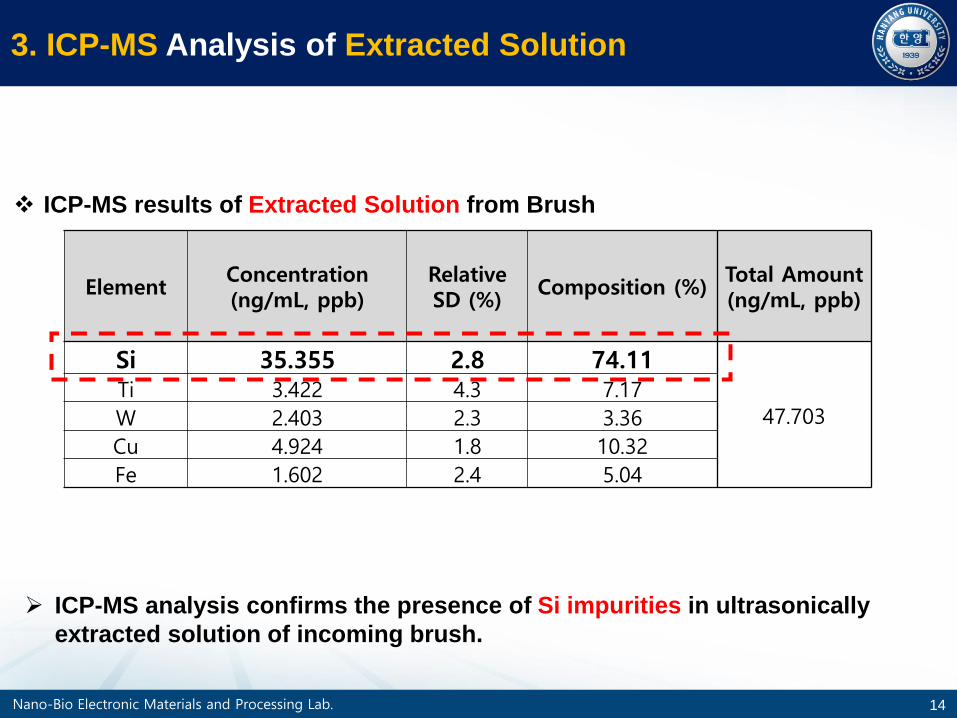
14Nano-Bio Electronic Materials and Processing Lab.
ElementConcentration(ng/mL, ppb)
Relative SD (%)
Composition (%)Total Amount(ng/mL, ppb)
Si 35.355 2.8 74.11
47.703
Ti 3.422 4.3 7.17
W 2.403 2.3 3.36
Cu 4.924 1.8 10.32
Fe 1.602 2.4 5.04
3. ICP-MS Analysis of Extracted Solution
ICP-MS results of Extracted Solution from Brush
ICP-MS analysis confirms the presence of Si impurities in ultrasonically
extracted solution of incoming brush.
15Nano-Bio Electronic Materials and Processing Lab.
4. LC-MS Analysis of Extracted Solution
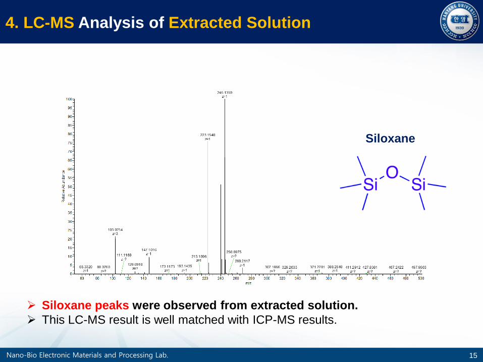
Siloxane peaks were observed from extracted solution.
This LC-MS result is well matched with ICP-MS results.
Siloxane
16Nano-Bio Electronic Materials and Processing Lab.
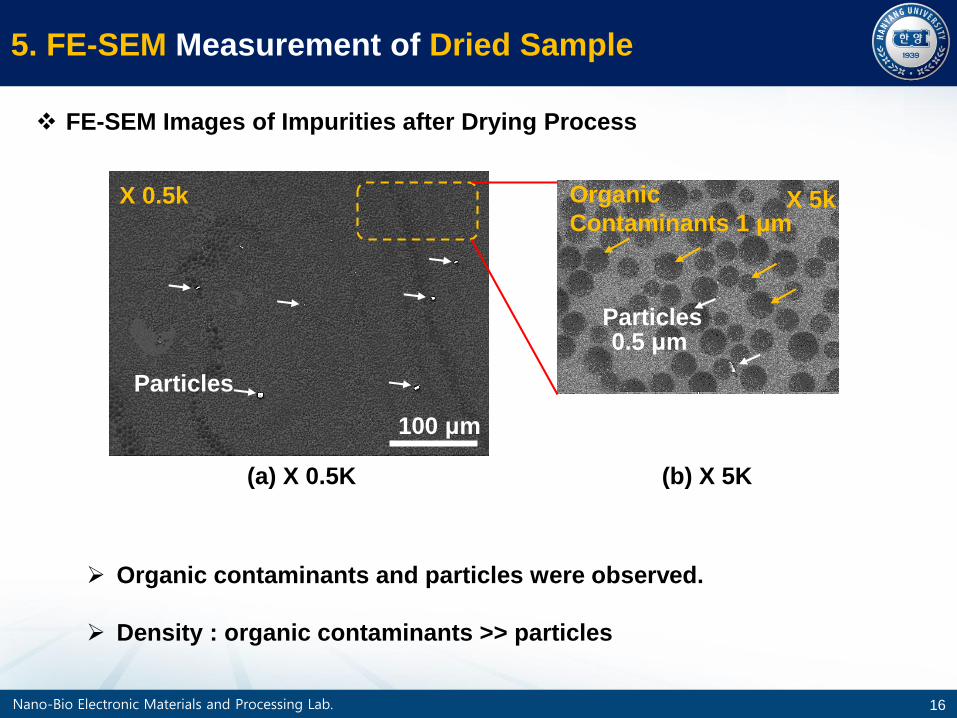
FE-SEM Images of Impurities after Drying Process
5. FE-SEM Measurement of Dried Sample
X 0.5k
Particles
100 μm
Organic
Contaminants 1 μm
0.5 μmParticles
(a) X 0.5K (b) X 5K
X 5k
Organic contaminants and particles were observed.
Density : organic contaminants >> particles
17Nano-Bio Electronic Materials and Processing Lab.
X 50k
589 nm258 nm
X 100k
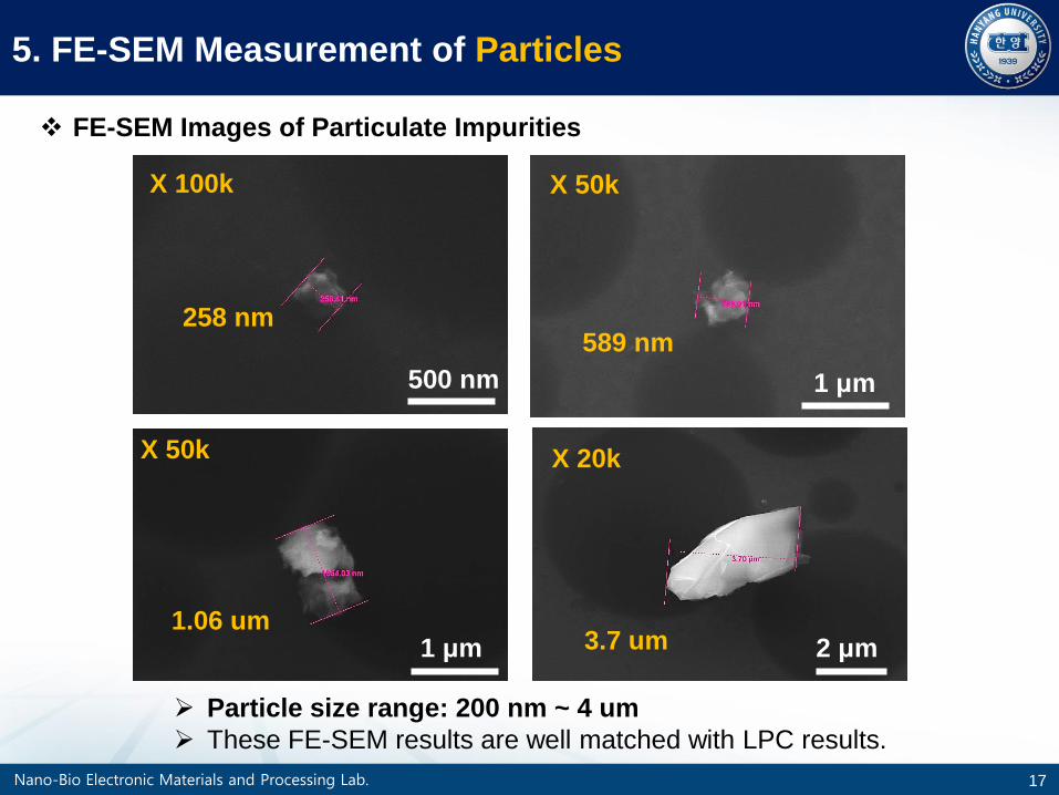
5. FE-SEM Measurement of Particles
X 50k
1.06 um
X 20k
3.7 um
500 nm 1 μm
1 μm 2 μm
Particle size range: 200 nm ~ 4 um
These FE-SEM results are well matched with LPC results.
FE-SEM Images of Particulate Impurities
18Nano-Bio Electronic Materials and Processing Lab.
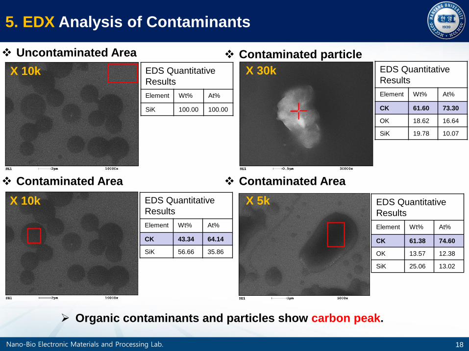
Uncontaminated Area
Contaminated Area Contaminated Area
Contaminated particle
Organic contaminants and particles show carbon peak.
EDS Quantitative
Results
Element Wt% At%
SiK 100.00 100.00
EDS Quantitative
Results
Element Wt% At%
CK 61.60 73.30
OK 18.62 16.64
SiK 19.78 10.07
EDS Quantitative
Results
Element Wt% At%
CK 61.38 74.60
OK 13.57 12.38
SiK 25.06 13.02
EDS Quantitative
Results
Element Wt% At%
CK 43.34 64.14
SiK 56.66 35.86
5. EDX Analysis of Contaminants
X 10k
X 10k X 5k
X 30k
19Nano-Bio Electronic Materials and Processing Lab.
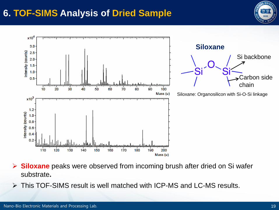
6. TOF-SIMS Analysis of Dried Sample
Siloxane peaks were observed from incoming brush after dried on Si wafer
substrate.
This TOF-SIMS result is well matched with ICP-MS and LC-MS results.
Siloxane
Siloxane: Organosilicon with Si-O-Si linkage
Si backbone
Carbon side
chain
20Nano-Bio Electronic Materials and Processing Lab.
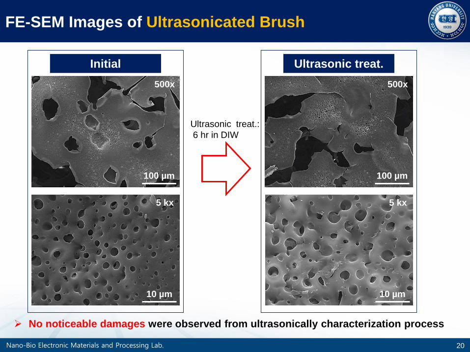
FE-SEM Images of Ultrasonicated Brush
100 µm
500x
10 µm
5 kx
Initial Ultrasonic treat.
100 µm
500x
10 µm
5 kx
Ultrasonic treat.:
6 hr in DIW
No noticeable damages were observed from ultrasonically characterization process
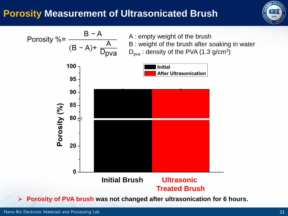
21Nano-Bio Electronic Materials and Processing Lab.
0
20
80
85
90
95
100
Po
ros
ity (
%)
Initial
After Ultrasonication
Porosity Measurement of Ultrasonicated Brush
Initial Brush Ultrasonic
Treated Brush
Porosity of PVA brush was not changed after ultrasonication for 6 hours.
A : empty weight of the brush
B : weight of the brush after soaking in water
Dpva : density of the PVA (1.3 g/cm3)
22Nano-Bio Electronic Materials and Processing Lab.
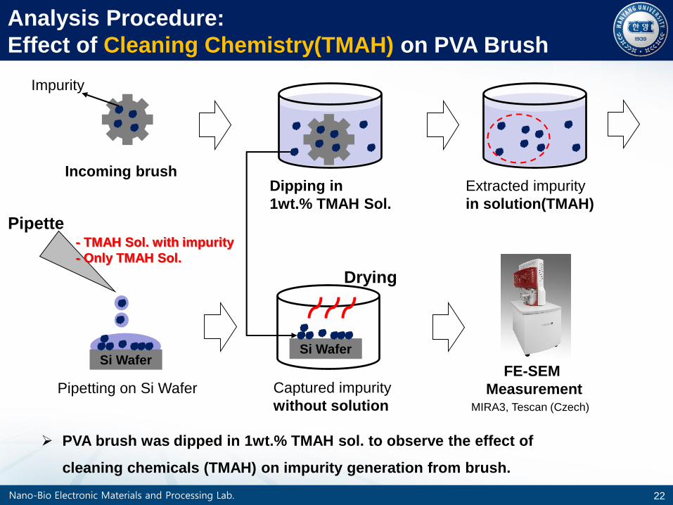
Si Wafer
Incoming brushDipping in
1wt.% TMAH Sol.
Extracted impurity
in solution(TMAH)
Captured impurity
without solution
Drying
Analysis Procedure:
Effect of Cleaning Chemistry(TMAH) on PVA Brush
FE-SEM
MeasurementMIRA3, Tescan (Czech)
Si Wafer
Pipette
Pipetting on Si Wafer
Impurity
- TMAH Sol. with impurity
- Only TMAH Sol.
PVA brush was dipped in 1wt.% TMAH sol. to observe the effect of
cleaning chemicals (TMAH) on impurity generation from brush.
23Nano-Bio Electronic Materials and Processing Lab.
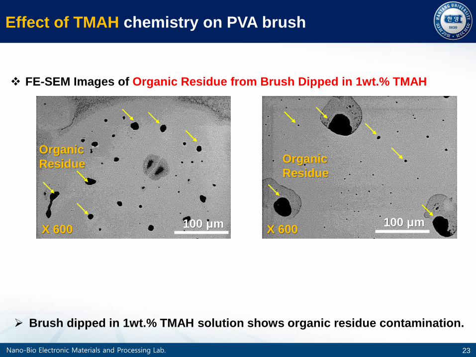
X 600 X 600
FE-SEM Images of Organic Residue from Brush Dipped in 1wt.% TMAH
Brush dipped in 1wt.% TMAH solution shows organic residue contamination.
Organic
Residue
Effect of TMAH chemistry on PVA brush
100 μm 100 μm
Organic
Residue
24Nano-Bio Electronic Materials and Processing Lab.
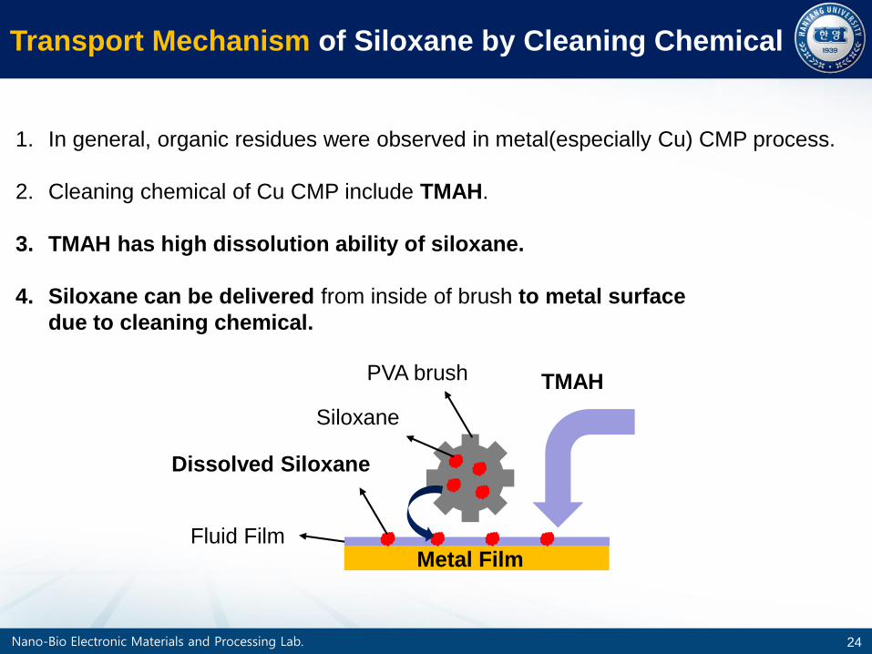
Transport Mechanism of Siloxane by Cleaning Chemical
1. In general, organic residues were observed in metal(especially Cu) CMP process.
2. Cleaning chemical of Cu CMP include TMAH.
3. TMAH has high dissolution ability of siloxane.
4. Siloxane can be delivered from inside of brush to metal surface
due to cleaning chemical.
TMAH
Metal FilmFluid Film
PVA brush
Siloxane
Dissolved Siloxane
25Nano-Bio Electronic Materials and Processing Lab.
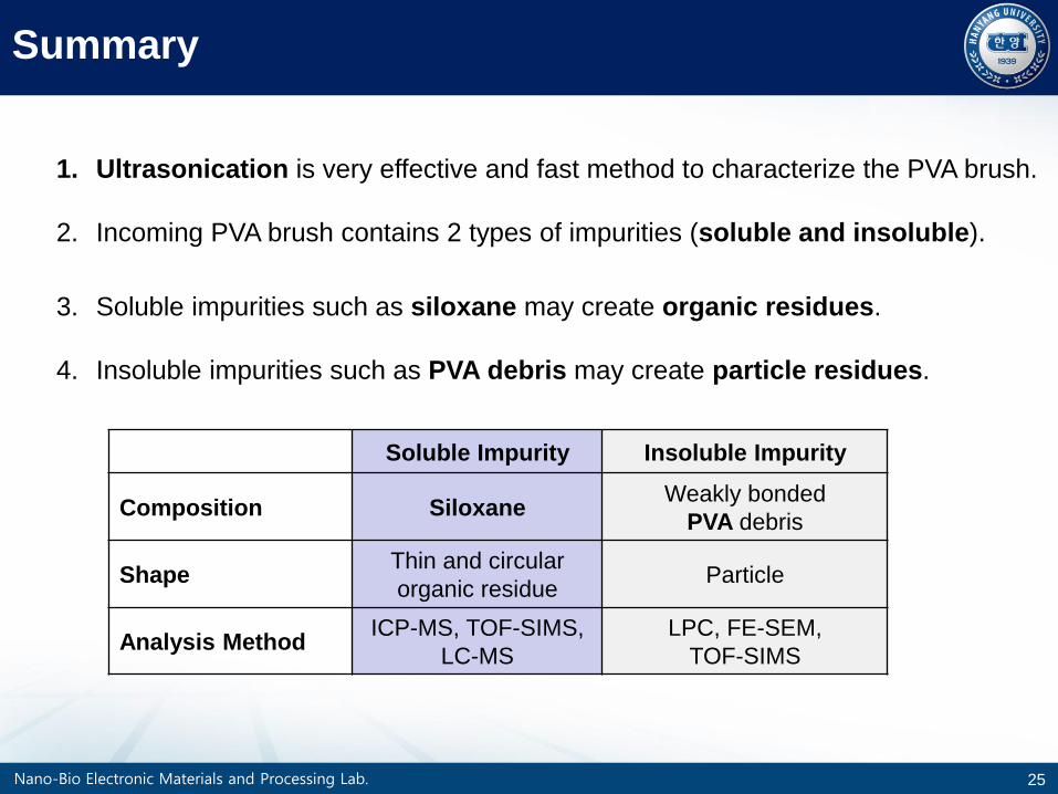
Summary
1. Ultrasonication is very effective and fast method to characterize the PVA brush.
2. Incoming PVA brush contains 2 types of impurities (soluble and insoluble).
3. Soluble impurities such as siloxane may create organic residues.
4. Insoluble impurities such as PVA debris may create particle residues.
Soluble Impurity Insoluble Impurity
Composition SiloxaneWeakly bonded
PVA debris
ShapeThin and circular
organic residueParticle
Analysis MethodICP-MS, TOF-SIMS,
LC-MS
LPC, FE-SEM,
TOF-SIMS
26Nano-Bio Electronic Materials and Processing Lab.
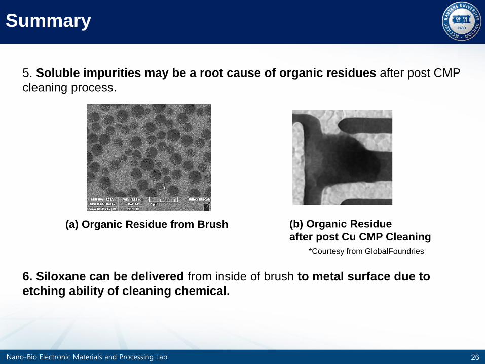
Summary
5. Soluble impurities may be a root cause of organic residues after post CMP
cleaning process.
(a) Organic Residue from Brush (b) Organic Residue
after post Cu CMP Cleaning
6. Siloxane can be delivered from inside of brush to metal surface due to
etching ability of cleaning chemical.
*Courtesy from GlobalFoundries

Nano-Bio Electronic Materials and Processing Lab.