Embed Size (px)
Citation preview
1
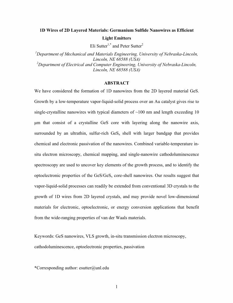
1D Wires of 2D Layered Materials: Germanium Sulfide Nanowires as Efficient
Light Emitters
Eli Sutter1,* and Peter Sutter2 1Department of Mechanical and Materials Engineering, University of Nebraska-Lincoln,
Lincoln, NE 68588 (USA) 2Department of Electrical and Computer Engineering, University of Nebraska-Lincoln,
Lincoln, NE 68588 (USA)
ABSTRACT
We have considered the formation of 1D nanowires from the 2D layered material GeS.
Growth by a low-temperature vapor-liquid-solid process over an Au catalyst gives rise to
single-crystalline nanowires with typical diameters of ~100 nm and length exceeding 10
µm that consist of a crystalline GeS core with layering along the nanowire axis,
surrounded by an ultrathin, sulfur-rich GeSx shell with larger bandgap that provides
chemical and electronic passivation of the nanowires. Combined variable-temperature in-
situ electron microscopy, chemical mapping, and single-nanowire cathodoluminescence
spectroscopy are used to uncover key elements of the growth process, and to identify the
optoelectronic properties of the GeS/GeSx core-shell nanowires. Our results suggest that
vapor-liquid-solid processes can readily be extended from conventional 3D crystals to the
growth of 1D wires from 2D layered crystals, and may provide novel low-dimensional
materials for electronic, optoelectronic, or energy conversion applications that benefit
from the wide-ranging properties of van der Waals materials.
Keywords: GeS nanowires, VLS growth, in-situ transmission electron microscopy,
cathodoluminescence, optoelectronic properties, passivation
*Corresponding author: [email protected]

2
1. INTRODUCTION
Semiconductor nanowires have attracted significant interest due to quantum size
effects and novel properties they promise to bring to a wide range of electronic and
optoelectronic devices,1-3 chemical and biological sensors,4 artificial photosynthesis,5
solar energy conversion,6-7 and photovoltaic systems.8 The majority of semiconductor
nanowires have been synthesized from three-dimensional (3D) materials such as Si, Ge,
GaAs, etc. Beyond these traditional semiconductors, interesting new electronic or
optoelectronic functionality may become accessible in nanowires consisting of van der
Waals materials. Recently, quasi-1D chalcogenides such as Ta2Pd3Se8 or TaSe3 have
been isolated by exfoliation from the bulk and first studies of their properties,
semiconducting for Ta2Pd3Se8,9 metallic or semimetallic in the case of TaSe3,10 have been
reported, so far for fibers or bundles in which larger numbers of the elementary 1D units
are joined by weak van der Waals forces. While the morphology of these fibers or
nanowires is dictated by the 1D structure of their building blocks, an alternative avenue
toward quasi 1D van der Waals materials is to shape a 2D layered crystal into a nanowire
geometry. A wire geometry may be achieved by adapting bottom-up synthesis protocols
that are well-established for nanowires from 3D materials, such as vapor-liquid-solid
(VLS) growth.11 Such an approach has the added advantages of producing large numbers
of wires grown in parallel, and of defining the wire diameter via the size of a growth
catalyst.12-13 Here we discuss the bottom-up synthesis of nanowires of the layered
semiconductor germanium sulfide (GeS) and establish the growth mechanism, structure,
stability, and optoelectronic properties of these GeS wires.

3
GeS is a layered material with structure analogous to that of black phosphorus and
a bandgap in the visible region (1.65 – 1.8 eV).14-18 The anisotropic crystal structure of
GeS gives rise to anisotropy in the optoelectronic properties, such as polarized optical
absorption,14, 18 photoconductivity,19 etc. One important property of GeS is its much
lower toxicity and environmental impact when compared with other semiconductors, e.g.,
those containing heavy metals such as cadmium or lead.20 GeS nanoparticles have
demonstrated excellent cycling performance for Li-ion batteries applications.21 GeS
nanosheets and nanoribbons have emerged as important IV/VI semiconductor materials
with potential in electronic and opto-electronics applications22 for telecommunications,
computing, as visible light photodetectors with high sensitivity and broad spectral
response,22-24 and as a photo-absorbers for use in solar energy conversion.25 Recent work
has shown unusual electronic properties, including multiferroic behavior with coupled
ferroelectricity and ferroelasticity,26-27 and potential for third generation photovoltaics
based on shift-currents.28 In nanosheets and nanoribbons thickness-dependent properties,
i.e., absorption dominated by tightly bound excitons with remarkably large binding
energy of 1 eV similar to other 2D materials are expected to give rise to new phenomena
in the ultrathin limit.29 GeS nanosheets and nanoribbons have been prepared by a variety
of methods: chemical vapor transport followed by mechanical exfoliation,22, 30 chemical
vapor deposition (CVD),23, 31 and colloidal synthesis.16, 32-33
GeS nanowires (NWs) have previously been prepared by vapor transport34 as well
as by liquid chemical synthesis,35-36 but an understanding of the growth mechanism,
stability, and of their properties at the level of individual nanowires has not been
developed. Here we discuss the synthesis of high quality GeS NWs using a low

4
temperature vapor-liquid-solid (VLS) process. We establish the structure of the as-grown
nanowires and use transmission electron microscopy (TEM) based methods such as
chemical mapping and in-situ observations of individual NWs during annealing near the
growth temperature to reconstruct key elements of the VLS process, the stability of the
GeS NWs, formation and decomposition pathways, and the role and behavior of the
catalyst drop at the NW tip. Finally, we use cathodoluminescence in scanning
transmission electron microscopy (STEM-CL) with spatial resolution below the
diffraction limit to establish the optoelectronic properties of individual GeS NWs.
2. RESULTS AND DISCUSSION
GeS nanowires were grown in a two-zone tube furnace by thermal evaporation of
GeS powder using Ar-2% H2 as a carrier gas (see Methods for details). The Si(100)
substrates were covered by a thin Au film, which dewets at the growth temperature (270-
300°C)37 to generate a polydisperse array of supported Au nanoparticles.
Figure 1 shows the typical structure and morphology of individual GeS NWs
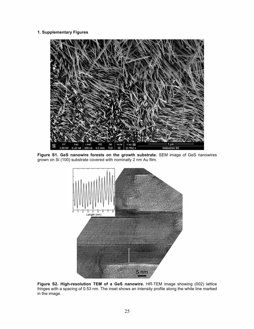
grown at a temperature of 280°C. The as-grown NW forests attached to the Si(100)
substrate are shown in the scanning electron microscopy (SEM) image of the
Supplementary Figure S1. The NWs typically have diameters in the range between 50-
120 nm and grow up to several tens of micrometers long. Figures 1 (a) – (b) show high-
angle annular dark field STEM (HAADF-STEM) images of a GeS NW segment on
amorphous carbon support illustrating the high aspect ratio and constant diameter of the
NWs over extended distances. High-resolution TEM images of the NWs (Figure S2)
show lattice fringes with a separation of 0.53 nm perpendicular to the NW axis,
consistent with the spacing of (002) planes in bulk GeS.38 Selected area electron

5
diffraction (Figure 1 (c)) shows that the wires are monocrystalline with their axes aligned
along the [001] direction, i.e., are stacks of GeS sheets with lateral dimensions limited to
the NW diameter arranged with their c-axis (the van der Waals stacking direction) along
the symmetry axis of the NWs (Figure 1 (d)).
Figure 1. Morphology of GeS nanowires. (a) HAADF-STEM overview image of GeS NWs on amorphous carbon film (Growth temperature: 280°C). (b) Higher magnification HAADF-STEM image of the section of the GeS NW marked by a rectangle in (a). (c) Electron diffraction pattern of the GeS NW along the [110] zone axis. (d) Schematic representation of the layered structure of the GeS nanowires.
Figure 2 shows a HAADF-STEM image close to the tip of a GeS NW (diameter
~110 nm). The NW shows uniform contrast along its length, suggesting a homogeneous
composition. Areas of brighter HAADF-STEM contrast, i.e., higher average atomic
number Z, are located at the NW tip and in small nanoparticles dispersed on the NW
surface. Energy dispersive x-ray spectroscopy (EDS) was used to determine the chemical
composition of the NWs and of these high-Z regions. Elemental maps and spectra
confirm the presence Ge and S along the NW (Figure 2 (b) – (g)), while the NW tip
contains Au in addition to Ge and S (Figure 3).

6
Figure 2. (a) HAADF-STEM image of a representative GeS nanowire near the Au-rich tip. (b) – HAADF-STEM image and (c) – (e) EDS chemical maps of the GeS NW showing the distribution of S (red), Ge (green), and Au (blue) (f) Overlaid S, Ge and Au maps. (g) EDS spectrum from the NW, yielding a composition of 50.2 at.% Ge and 49.8 at% S.
The chemical maps show a uniform distribution of Ge and S in the NWs (Figure 2
(c) – (f)). The quantification of spectra confirms a Ge:S atomic ratio of 1:1,
corresponding to Ge monosulfide (GeS, Figure 2 (g)). Au incorporation in the NWs is
below the EDS detection limit. Note that the weak signal detected in the Au EDS map
across the entire NW actually originates from the tail of the S K-a EDS peak (centered at
e = 2.3 keV), which is close to the Au M peak (2.1 keV) mapped in Figure 2 (e). Intense
Au signal is detected in the small nanoparticles on the NW surface, which are likely the
result of Au runoff from the catalyst at the tip during cooling to room temperature,
similar to VLS-grown Ge NWs.39-40 Chemical characterization of the nanoparticle at the
NW tip shows that its composition is inhomogeneous (Figure 3), comprising distinct
parts that are Au-rich and Ge-rich, respectively. The Au-rich section contains substantial
amounts of S as well as some Ge. The Ge-rich part of the tip, on the other hand, shows
very low S and Au content.

7
Figure 3. Representative HAADF-STEM image and EDS S (red), Ge (green), and Au (blue) and overlaid maps of a GeS NW tip.
The presence of telltale Au-rich catalyst particles at the tips of our GeS NWs
suggests that their growth proceeds either via a vapor-liquid-solid (VLS)34 or a vapor-
solid-solid (VSS) process.41 In both of these processes, Au nanoparticles play the role of
growth seeds and transport media whose interface to the semiconductor wire represents
the NW growth front. In VLS growth, the temperature is maintained above the eutectic
temperature (TE) or raised above TE and then dropped to produce a liquid alloy drop.
Surface adsorption on the drop establishes a concentration gradient of the semiconductor
component in the liquid alloy, and diffusion through the drop causes a small
supersaturation that drives the incorporation of new semiconductor material at the NW
interface. In VSS growth the temperature is kept below the eutectic temperature and the
catalyst is in the solid state, which results in much slower NW growth rates. At first
glance, the low substrate temperatures (270°C) used in our experiments – lower than any
eutectic temperature in the ternary Au-S-Ge alloy phase diagram – might indicate growth
via a VSS process. A second possibility is that the ternary Au-S-Ge alloy might have a
lower melting temperature at the nanoscale than in the bulk. Such deviations are not
uncommon. For binary Au-Ge alloys, for instance, size-dependent behavior such as a
lowered liquidus line and enhanced Ge solubility have been established previously using
in-situ annealing experiments, and this previous work established conditions for
observing melting and crystallization of the binary alloy drop.13, 37, 42-43 Here we

8
performed similar in-situ experiments to obtain information on the growth of our GeS
NWs, such as the underlying process (VLS or VSS), the temperature-dependent behavior
(e.g., melting temperature affected by the presence of sulfur) of the Au-Ge-S tip, the
elementary growth species (e.g., elemental Ge and S, or GeS molecules), and the role of
the anisotropic crystal structure of GeS in growth and decomposition. Important for
practical applications, the in-situ observations at variable temperature establish the
thermal regime where layered GeS NWs are stable and possible new morphologies that
may be accessed via controlled decomposition.
Since the catalyst particle at the NW tip holds the key to understanding the growth
mechanisms, we investigated its composition and phase behavior using variable-
temperature TEM. Figure 4 shows a section of a NW close to its tip during annealing
from room temperature to 270°C. The NW tip initially remains solid and unchanged from
its room-temperature morphology up to ~220°C. Above 230°C, parts of the tip start
rearranging and at ~250°C large parts of the tip are molten (similar to Au-Ge-Sb drops at
the tips of Ge NWs).44 A small part remains solid even at 270°C, the highest temperature
of our observations. Comparison with EDS maps (Figure 3) shows that it is the Ge-rich
(or pure Ge) section of the tip that remains solid even at 270°C, consistent with the higher
eutectic temperature for a Au-Ge alloy (361°C) or melting temperature of a Ge
nanocrystal. Investigations at higher temperatures were hindered by a rapid thermal
decomposition of the NWs (see below). Upon cooling to room temperature the molten tip
solidifies again (Figure 4 – right, 20°C).

9
Figure 4. Sequence of TEM images showing the GeS NW close to its tip during in-situ annealing up to 270°C, followed by cooling to room temperature.
The Au-rich part of the NW tip contains significant amounts of both S and Ge
even after the in-situ melting and re-crystallization. Previous work has shown that the
melting and crystallization behavior of binary Au-Ge alloy drops depends on the Ge
content: near eutectic composition all Ge is expelled upon crystallization,11, 35 whereas
this phase separation is frustrated at higher Ge content where crystallization instead
produces metastable AuGe phases.45 In the case of Au catalyzed GeS NWs, the presence
of Ge and S in the Au-rich part of the tip demonstrates that not all GeS is expelled from
the drop during cooling to room temperature. Strikingly, the melting temperature
determined in the in-situ experiments is below ~250°C. The bulk Au-Ge-S ternary phase
diagram predicts the appearance of the first liquid phase at T = 358°C, in the form of a
Au-Ge eutectic in coexistence with a solid GeS phase.46 Below 358°C the only liquid
phase involves molten S coexisting with solid Au-Ge. The in-situ TEM experiments
show that the Au-Ge-S tip melts at temperatures substantially below any predicted by the
bulk phase diagram and is molten well below our GeS NWs growth temperatures,
suggesting that the underlying growth process is VLS rather than VSS. The high growth
rates (>1-2 µm/minute, as determined from the average NW length and growth duration)
also suggest a VLS rather than a VSS process.
10
As mentioned above, the GeS NWs tend to decompose rapidly when heated above
~250°C. We designed in-situ annealing experiments in TEM to obtain additional
information about the growth and structure from this thermal decomposition of the NWs.
In principle, there are two different pathways for this process: i) Via continuous loss of S,
accompanied by defect (S vacancy) formation until pure Ge is left behind, analogous to
the transformation of other chalcogenides (e.g., SnS2 to SnS47); or ii) by simultaneous
loss of Ge and S, holding the NW composition fixed at GeS. Figure 5 follows the changes
to GeS NWs during annealing (see also Supplementary Movies M1 – M3). For
temperatures above 230°C, the contrast of the NWs changes with lighter areas
developing and growing with time. This contrast change is associated with the loss of
material from the wires. Following the thermal decomposition at temperatures between
230 and 260°C, we find that the process proceeds through identical steps and is merely
slower at lower temperatures. Starting from an initially intact GeS NW (Figure 5 (a)), the
onset of decomposition is clearly marked by the development of small areas of lighter
contrast with rectangular or square shape developing over the surface of the NW (Figures
5 (b), (c)). These areas progressively increase in size until the entire NW is nearly
completely decomposed and only a thin, empty shell is left behind. The loss of material is
clearly anisotropic. It proceeds fastest in the [100] and [010] directions (i.e., by
detachment from the basal plane edges) but our movies (M1 – M3) show that it also
extends along the [001] direction (i.e., across the van der Waals gaps between these
planes). The comparison between movies obtained at different projection of the NWs
(~[100] for movie M1; ~[010] for movie M3) along with imaging of individual wires at
different sample tilts (Figure S3) and measurements of the decomposition rates (Figure

11
S4) suggest an anisotropic decomposition with different detachment rates along the a-
and b-axes of the GeS sheets, as well as a finite removal rate along the c-axis. The
observations confirm that detachment starts at the edges (i.e., low-coordination sites) and
generally proceeds into the sheet more easily than across to the neighboring sheets, which
requires the nucleation of vacancies within the initially defect-free sheet. For anisotropic
crystals such as GeS, different edge detachment barriers from armchair and zigzag edges
may cause inhomogeneous thinning along a- and b-axes, which is indeed seen in our
images.
EDS maps and spectra of annealed GeS NWs provide further insight into the
decomposition process. A decreasing EDS signal intensity is consistent with the observed
loss of material (Figure S5). Spectra taken at different stages of decomposition show that
the NW composition is preserved, demonstrating that the thinning proceeds with a net
loss of both germanium and sulfur at equal rates. This behavior is consistent with the
reported high stability of GeS molecules,48 demonstrated by the fact that in thermal
evaporation of GeS powders or crystals the mass signal detected in the vapor stems solely
from GeS molecules that are evaporated from the NWs as an intact unit.
The observed local thinning rather than a uniform mass loss across the entire wire
surface is likely due to the presence of a thermally stable, ultrathin shell covering the
NWs, which may cause local differences in the decomposition rates. This surface shell is
not the result of oxidation. GeOx would readily be reduced already at temperatures as low
as 200°C,37, 43, 49 and our EDS data do not show a significant oxygen peak (see Figure S5).
Measurements of the composition of these empty shells show that they contain Ge and S,
but have higher S content than the GeS NWs. Thus the decomposition of the GeS NW

12
leaves behind an empty GeSx “nanotube” that remains stable during annealing. Single
NW luminescence measurements discussed below (Figure 6) show that this S-rich GeSx
shell does not form during the annealing but is present – albeit difficult to detect by
structural imaging or chemical mapping – already on the as-grown NWs and hence must
be generated during the NW synthesis. Our findings differ in two key aspects from
previously reported GeS2 NWs:50 (i) The present NWs are core-shell structures with a
GeS core surrounded by an ultrathin sulfur-rich shell; and (ii) luminescence suggests that
the shell has GeSx stoichiometry intermediate between GeS and GeS2.
Figure 5. Sequence of TEM images of a GeS NW during annealing at 260°C over a period of 9 min. (a) – (h) In-situ TEM image image sequence showing the evolution of small rectangular-shaped thin areas in the GeS NW with time. The projection is approximately along the [100] direction of the GeS lattice. (i) High resolution TEM image at an intermediate stage of the GeS NW decomposition. The NW axis runs parallel to the c-axis of the GeS lattice.
The combined data from our structural analysis and from the annealing studies on
the wires and the Au-rich catalyst particles at their tips allow us to assemble a consistent
picture of the GeS NW growth process. The NWs grow by a low-temperature VLS
process with a liquid, Au-rich drop as catalyst. Given that the catalyst contains both Ge
and S, we conclude that during NW growth from GeS vapor the tip incorporates GeS
molecules, which diffuse through the liquid drop and crystallize into a GeS NW,

13
analogous to the growth of other compound semiconductor NWs (GaAs, InP, etc.) from
pseudo-binary alloys phases.51-52 Predominant mass transport via stable GeS units is
further confirmed by in-situ TEM experiments on the thermal decomposition of the GeS
NWs. While this VLS process leads to the formation of the GeS NW core, the in-situ
annealing experiments provide clear evidence for the presence of a thin GeSx shell with
higher S content. EDS maps showing a Ge-rich phase in the catalyst provide the key to
understanding the formation mechanism of this shell. While most of the supplied GeS is
transported through the drop intact, a small fraction appears to be dissociated into Ge and
S. While the Ge accumulates in the catalyst, the S is incorporated into the NW surface
during growth. Given its fixed stoichiometry, the GeS core apparently is unable to
accommodate the excess sulfur, and it is thus dissipated by incorporation into an ultrathin
surface shell. Assuming a shell with composition close to GeS2, the amount of residual
Ge in the tip after growth yields an estimated shell thickness of ~1 nm (see Supplement,
Figure S6). Importantly, this shell provides an efficient passivation against any chemical
changes in the NWs over months (Figure S7).53
To evaluate the optoelectronic properties of the GeS-GeSx core-shell NWs, we
performed cathodoluminescence (CL) spectroscopy in STEM. The high spatial resolution
of STEM-CL enabled the acquisition of luminescence spectra and of spectrum scans
across individual wires. There have been few reports of photoluminescence of GeS. Early
absorption measurements give a bandgap of GeS between 1.6 and 1.8 eV.14-18 Similar
values were found more recently in diffuse reflectance measurements on GeS
nanosheets.32 GeS flakes exfoliated from bulk crystals showed a single PL peak at 1.66
eV, a decreasing PL intensity with decreasing flake thickness, and a distinct anisotropy in

14
the optical absorption demonstrated by rotating the polarization with respect to the crystal
axes.30 Ensembles of thick (200 nm diameter) nominally GeS NWs showed a wide PL
peak centered at high energy 2.64 eV (470 nm), close to the absorption edge of GeS2
nanoplates detected at 2.75 eV (450 nm),35 but no emission at lower photon energies was
detected. This strongly suggests that PL of these NWs was dominated by GeS2, which
was indeed detected by X-ray diffraction as well.
Figure 6. STEM-CL on individual as-grown and annealed GeS NWs. (a) STEM image of a section of an as-grown GeS NW. (b) Panchromatic CL map of the GeS NW shown in (a). The false color scale is given on the right. (c) Spectrum imaging linescan across the NW, as marked in (a). The abscissa (wavelength, l or photon energy, hn) is the same as in (c). (d) Local luminescence spectra from the center (dashed) and periphery (solid) of the NW (at positions indicated in (c)).
Figure 6 shows CL maps and spectra obtained on individual as-grown GeS NWs.
The wires show intense luminescence across the visible parts of the spectrum. In
panchromatic CL maps, a pronounced maximum in emission intensity is observed near
the surface of the NWs, which in projection is seen as two intense bands near the top and
bottom edges of the wire (Figure 6 (a), (b)). Sets of CL spectra collected along a line
across the NW (as shown in Figure 6 (c), (d)) can explain this intensity distribution. Two
main emission peaks at ~645 and 685 nm (i.e., ~1.92 and 1.80 eV) are detected in the
center of the as-grown NWs, close to peaks observed previously in unpolarized room
temperature absorption spectra on bulk GeS.54 Significant emission extends in a tail to
longer wavelengths. These data are consistent with luminescence from the GeS core of

15
the NWs. In the near-surface region, a distinctly different characteristic is found. In
addition to the two peaks also present in the NW core emission, we find an additional,
broader emission peak centered at ~515 nm (i.e., 2.40 eV), which is clearly associated
with the GeSx shell. Interestingly, the emission peaks found in the GeS core appear with
higher intensity near the surface. This finding suggests an enhanced radiative
recombination due to electronic passivation by the ultrathin wide-bandgap GeSx shell,
which effectively reflects minority carriers toward the GeS core, i.e., away from possible
non-radiative recombination centers at the NW surface. This passivation due to the wide-
bandgap shell – and possibly also a reduced effect in layered materials of impurities that
would give rise to deep level recombination centers in ordinary semiconductors – thus
explains the absence of luminescence quenching due to surface recombination or due to
trap states that might be induced by the Au particles located on the NW surface.
3. CONCLUSIONS
In summary, we have studied the formation of 1D nanowires from the 2D layered
material GeS. Growth by a low-temperature vapor-liquid-solid process over an Au
catalyst gives rise to single-crystalline nanowires with typical diameters of ~100 nm and
length exceeding 10 µm that predominantly consist of GeS that is layered along the
nanowire axis. In-situ electron microscopy of the thermal decomposition of the nanowires
suggests that individual intact GeS units are thermally stable at the growth temperature,
and are the predominant mobile species adsorbed on and transported through the Au-
based catalyst drop during the vapor-liquid-solid growth process. The involved nanoscale
pseudo-binary (Au/GeS) phase appears to have an extremely low melting point, identified
here by variable-temperature in-situ microscopy to be ~250°C, which enables growth via

16
a liquid catalyst at temperatures substantially below those used for nanowire growth in
related materials systems (e.g., Au-Ge). For nanowires consisting of layered materials,
one might raise concerns about a possible detrimental role of a large number of dangling
bonds at the edges of the layers, especially in the configuration found here, namely with
layering perpendicular to the long axis of the wires. By combining observations of the
nanowire decomposition with results from local luminescence spectroscopy, we identify
an ultrathin shell, consisting of more sulfur-rich GeSx, around the layered GeS core. This
finding implies that layered VLS nanowires may be able to self-passivate dangling bonds
at their surface during growth. In the present case, the morphology of the catalyst at the
GeS nanowire tip – comprising a part that is highly enriched in Ge – suggests that an
ultrathin passivating shell is generated during growth by incorporation of sulfur liberated
by the dissociation of a small fraction of the adsorbing GeS in the catalyst drop. Our
results suggest that vapor-liquid-solid processes lend themselves well to the growth of 1D
wires from 2D layered crystals, and that such processes may enable the generation of
novel low-dimensional materials for electronic, optoelectronic, or energy conversion
applications that benefit from the wide-ranging properties of van der Waals materials.
4. MATERIALS AND METHODS
GeS NWs were synthesized using GeS powder (99.99%, Sigma Aldrich) in an
experimental setup consisting of a pumped quartz tube furnace with two temperature
zones. The evaporation zone containing a quartz boat with the GeS powder was heated to
450°C, while the zone containing the substrate was heated to growth temperatures of
270-350°C. Si (100) covered with 2-4 nm thick Au films deposited by sputtering at room
temperature was used as substrate. Such Au films dewet at the growth temperature.37

17
During growth a H2 (2%)/Ar carrier gas flow was maintained at 50 standard cubic
centimeters per minute (sccm) at a pressure of 20 mTorr. The growth was typically
performed for 10 minutes resulting in the formation of NWs with lengths of several tens
of micrometers. The morphology of the NWs was investigated by transmission electron
microscopy (TEM) in an FEI Technai Osiris 80-200 ChemiSTEM field emission
microscope and an FEI Talos F200X equipped with a Gatan 652 high-temperature sample
holder. In-situ experiments in TEM cover the temperature range between room
temperature and 300°C at pressures below 10-7 torr. The electron irradiation intensity was
kept intentionally low (< 0.1 A/cm2) during our observations to prevent any uncontrolled
electron beam induced structural changes. Cathodoluminescence (CL) measurements
were performed in STEM mode (STEM-CL) using a Gatan Vulcan CL holder at room
temperature and 200 kV electron energy. The incident beam current for CL
measurements was typically 300-400 pA. The panchromatic CL map in figure 6 is
100´100 pixels with acquisition time of 100 ms per pixel. Spectrum line scans were
acquired by rastering the electron beam in small steps across individual NWs and
acquiring full CL spectra at each beam position.
5. ACKNOWLEDGEMENTS
This work was supported by the National Science Foundation, Division of Materials
Research, Solid State and Materials Chemistry Program under Grant No. DMR-1607795.
SUPPORTING INFORMATION AVAILABLE: Supplementary Figures S1-S7: SEM
of GeS nanowires on the growth substrate, TEM images and chemical maps of pristine
and thermally decomposed GeS nanowires, analysis of decomposition rates, EDS spectra

18
of as grown and long-term air exposed GeS nanowires. Supplementary Movies M1-M3:
In-situ microscopy of thermal decomposition of GeS nanowires.

19
REFERENCES: 1. Lu, W.; Xiang, J.; Timko, B. P.; Wu, Y.; Lieber, C. M. One-‐‑Dimensional Hole Gas in Germanium/Silicon Nanowire Heterostructures P Natl Acad Sci USA 2005, 102, 10046-‐‑10051. 2. Wang, D. W.; Wang, Q.; Javey, A.; Tu, R.; Dai, H. J.; Kim, H.; McIntyre, P. C.; Krishnamohan, T.; Saraswat, K. C. Germanium Nanowire Field-‐‑Effect Transistors with Sio2 and High-‐‑Kappa Hfo2 Gate Dielectrics Appl Phys Lett 2003, 83, 2432-‐‑2434. 3. Zhang, L.; Tu, R.; Dai, H. J. Parallel Core-‐‑Shell Metal-‐‑Dielectric-‐‑Semiconductor Germanium Nanowires for High-‐‑Current Surround-‐‑Gate Field-‐‑Effect Transistors Nano Lett 2006, 6, 2785-‐‑2789. 4. Kamins, T. I.; Sharma, S.; Yasseri, A. A.; Li, Z.; Straznicky, J. Metal-‐‑Catalysed, Bridging Nanowires as Vapour Sensors and Concept for Their Use in a Sensor System Nanotechnology 2006, 17, S291-‐‑S297. 5. Liu, C.; Dasgupta, N. P.; Yang, P. Semiconductor Nanowires for Artificial Photosynthesis Chemistry of Materials 2014, 26, 415-‐‑422. 6. Liu, S.; Tang, Z.-‐‑R.; Sun, Y.; Colmenares, J. C.; Xu, Y.-‐‑J. One-‐‑Dimension-‐‑Based Spatially Ordered Architectures for Solar Energy Conversion Chemical Society Reviews 2015, 44, 5053-‐‑5075. 7. Su, Y.; Liu, C.; Brittman, S.; Tang, J.; Fu, A.; Kornienko, N.; Kong, Q.; Yang, P. Single-‐‑Nanowire Photoelectrochemistry Nat Nano 2016, 11, 609-‐‑612. 8. Brittman, S.; Gao, H.; Garnett, E. C.; Yang, P. Absorption of Light in a Single-‐‑Nanowire Silicon Solar Cell Decorated with an Octahedral Silver Nanocrystal Nano Lett 2011, 11, 5189-‐‑5195. 9. Xue Liu; Jinyu Liu; Liubov Yu. Antipina; Jin Hu; Chunlei Yue; Ana M. Sanchez; Pavel B. Sorokin; Zhiqiang Mao; Wei, J. Direct Fabrication of Functional Ultrathin Single-‐‑Crystal Nanowires from Quasi-‐‑One-‐‑Dimensional Van Der Waals Crystals Nano Lett 2016, 16, 6188-‐‑6195. 10. Guanxiong Liu; Sergey Rumyantsev; Matthew A. Bloodgood; Tina T. Salguero; Michael Shur; Balandin, A. A. Low-‐‑Frequency Electronic Noise in Quasi-‐‑1d Tase3 Van Der Waals Nanowires Nano Lett 2017, 17, 377-‐‑383. 11. Wagner, R. S.; Ellis, W. C. Vapor‐Liquid‐Solid Mechanism of Single Crystal Growth Appl Phys Lett 1964, 4, 89-‐‑90. 12. Dayeh, S. A.; Picraux, S. T. Direct Observation of Nanoscale Size Effects in Ge Semiconductor Nanowire Growth Nano Lett 2010, 10, 4032-‐‑4039. 13. Sutter, E.; Sutter, P. Phase Diagram of Nanoscale Alloy Particles Used for Vapor−Liquid−Solid Growth of Semiconductor Nanowires Nano Lett 2008, 8, 411-‐‑414. 14. Wiley, J. D.; Breitschwerdt, A.; Schonherr, E. Optical-‐‑Absorption Band Edge in Single-‐‑Crystal Ges Solid State Commun 1975, 17, 355-‐‑359. 15. Bletskan, D. I.; Polazhinets, N. V.; Gal, M. M. Photoelectric Properties of Layered Crystals of Ges Doped with Sb Inorg Mater 1989, 25, 1375-‐‑1378.

20
16. Ramasamy, P.; Kwak, D.; Lim, D.-‐‑H.; Ra, H.-‐‑S.; Lee, J.-‐‑S. Solution Synthesis of Ges and Gese Nanosheets for High-‐‑Sensitivity Photodetectors Journal of Materials Chemistry C 2016, 4, 479-‐‑485. 17. Yabumoto, T. Electrical and Optical Properties of Ges J Phys Soc Jpn 1958, 13, 559-‐‑562. 18. Gamzaev, D. O.; Kulibekov, A. M.; Suleimanov, R. A. Light-‐‑Exciton Mixing Effects in Ges Inorg Mater 1992, 28, 1992-‐‑1994. 19. Wiley, J. D.; Pennington, S.; Schonherr, E. Anisotropy of the Intrinsic Photoconductivity of Ges Phys Status Solidi B 1979, 96, K43-‐‑K46. 20. Latiff, N.; Teo, W. Z.; Sofer, Z.; Huber, S.; Fisher, A. C.; Pumera, M. Toxicity of Layered Semiconductor Chalcogenides: Beware of Interferences Rsc Adv 2015, 5, 67485-‐‑67492. 21. Cho, Y. J.; Im, H. S.; Myung, Y.; Kim, C. H.; Kim, H. S.; Back, S. H.; Lim, Y. R.; Jung, C. S.; Jang, D. M.; Park, J.; Cha, E. H.; Choo, S. H.; Song, M. S.; Cho, W. I. Germanium Sulfide(Ii and Iv) Nanoparticles for Enhanced Performance of Lithium Ion Batteries Chemical Communications 2013, 49, 4661-‐‑4663. 22. Ulaganathan, R. K.; Lu, Y.-‐‑Y.; Kuo, C.-‐‑J.; Tamalampudi, S. R.; Sankar, R.; Boopathi, K. M.; Anand, A.; Yadav, K.; Mathew, R. J.; Liu, C.-‐‑R.; Chou, F. C.; Chen, Y.-‐‑T. High Photosensitivity and Broad Spectral Response of Multi-‐‑Layered Germanium Sulfide Transistors Nanoscale 2016, 8, 2284-‐‑2292. 23. Lan, C.; Li, C.; Yin, Y.; Guo, H.; Wang, S. Synthesis of Single-‐‑Crystalline Ges Nanoribbons for High Sensitivity Visible-‐‑Light Photodetectors Journal of Materials Chemistry C 2015, 3, 8074-‐‑8079. 24. Dhanabalan, S. C.; Ponraj, J. S.; Zhang, H.; Bao, Q. L. Present Perspectives of Broadband Photodetectors Based on Nanobelts, Nanoribbons, Nanosheets and the Emerging 2d Materials Nanoscale 2016, 8, 6410-‐‑6434. 25. Antunez, P. D.; Buckley, J. J.; Brutchey, R. L. Tin and Germanium Monochalcogenide Iv-‐‑Vi Semiconductor Nanocrystals for Use in Solar Cells Nanoscale 2011, 3, 2399-‐‑2411. 26. Fei, R.; Li, W.; Li, J.; Yang, L. Giant Piezoelectricity of Monolayer Group Iv Monochalcogenides: Snse, Sns, Gese, and Ges Appl Phys Lett 2015, 107, 173104. 27. Wu, M.; Zeng, X. C. Intrinsic Ferroelasticity and/or Multiferroicity in Two-‐‑Dimensional Phosphorene and Phosphorene Analogues Nano Lett 2016, 16, 3236−3241. 28. Kushnir, K.; Wang, M.; Fitzgerald, P. D.; Koski, K. J.; Titova, L. V. Ultrafast Zero-‐‑Bias Photocurrent in Ges Nanosheets: Promise for Photovoltaics ACS Energy Letters 2017, 2, 1429−1434. 29. Gomes, L. C.; Trevisanutto, P. E.; Carvalho, A.; Rodin, A. S.; Castro Neto, A. H. Strongly Bound Mott-‐‑Wannier Excitons in Ges and Gese Monolayers Physical Review B 2016, 94, 155428. 30. Tan, D.; Lim, H. E.; Wang, F.; Mohamed, N. B.; Mouri, S.; Zhang, W.; Miyauchi, Y.; Ohfuchi, M.; Matsuda, K. Anisotropic Optical and Electronic Properties of Two-‐‑Dimensional Layered Germanium Sulfide Nano Research 2017, 10, 546-‐‑555. 31. Li, C.; Huang, L.; Snigdha, G. P.; Yu, Y. F.; Cao, L. Y. Role of Boundary Layer Diffusion in Vapor Deposition Growth of Chalcogenide Nanosheets: The Case of Ges Acs Nano 2012, 6, 8868-‐‑8877.

21
32. Vaughn, D. D.; Patel, R. J.; Hickner, M. A.; Schaak, R. E. Single-‐‑Crystal Colloidal Nanosheets of Ges and Gese J Am Chem Soc 2010, 132, 15170-‐‑15172. 33. Vaughn, D. D.; Schaak, R. E. Synthesis, Properties and Applications of Colloidal Germanium and Germanium-‐‑Based Nanomaterials Chemical Society Reviews 2013, 42, 2861-‐‑2879. 34. Li, C.; Yu, Y. F.; Chi, M. F.; Cao, L. Y. Epitaxial Nanosheet-‐‑Nanowire Heterostructures Nano Lett 2013, 13, 948-‐‑953. 35. Lai, Z.; Guo, Y.; Yang, P. Facile Synthesis, Characterization, Nanocrystal Growth and Photoluminescence Properties of Ges Nanowires Nano 2016, 11, 1650140. 36. Shi, L.; Dai, Y. M. Synthesis, Formation Mechanism and Photoelectric Properties of Ges Nanosheets and Nanowires J Appl Crystallogr 2014, 47, 527-‐‑531. 37. Sutter, E.; Ozturk, B.; Sutter, P. Selective Growth of Ge Nanowires by Low-‐‑Temperature Thermal Evaporation Nanotechnology 2008, 19. 38. Wiedemeier, H.; Schnering, H. G. V. Refinement of the Structures of Ges, Gese, Sns and Snse Z Kristallogr 1978, 148, 295-‐‑303. 39. Sutter, E.; Sutter, P. Au-‐‑Induced Encapsulation of Ge Nanowires in Protective Carbon Shells Adv Mater 2006, 18, 2583. 40. Kamins, T. I.; Li, X.; Williams, R. S. Growth and Structure of Chemically Vapor Deposited Ge Nanowires on Si Substrates Nano Lett 2004, 4, 503. 41. Chou, Y. C.; Wen, C. Y.; Reuter, M. C.; Su, D.; Stach, E. A.; Ross, F. M. Controlling the Growth of Si/Ge Nanowires and Heterojunctions Using Silver-‐‑Gold Alloy Catalysts Acs Nano 2012, 6, 6407-‐‑6415. 42. Sutter, E. A.; Sutter, P. W. Size-‐‑Dependent Phase Diagram of Nanoscale Alloy Drops Used in Vapor-‐‑Liquid-‐‑Solid Growth of Semiconductor Nanowires Acs Nano 2010, 4, 4943-‐‑4947. 43. Sutter, P. W.; Sutter, E. A. Dispensing and Surface-‐‑Induced Crystallization of Zeptolitre Liquid Metal-‐‑Alloy Drops Nat Mater 2007, 6, 363-‐‑366. 44. Sutter, E.; Sutter, P. Vapor-‐‑Liquid-‐‑Solid Growth and Sb Doping of Ge Nanowires from a Liquid Au-‐‑Sb-‐‑Ge Ternary Alloy Appl Phys a-‐‑Mater 2010, 99, 217-‐‑221. 45. Sutter, E.; Sutter, P. Formation and Stabilization of Single-‐‑Crystalline Metastable Auge Phases in Ge Nanowires Nanotechnology 2011, 22. 46. Moh, G. H.; Kullerud, G. Gold-‐‑Germanium-‐‑Sulfur Ternary Alloy Phase Diagram Neues Jahrbuch Fur Mineralogie-‐‑Abhandlungen 1986, 153, 307-‐‑310. 47. Sutter, E.; Huang, Y.; Komsa, H. P.; Ghorbani-‐‑Asl, M.; Krasheninnikov, A. V.; Sutter, P. Electron-‐‑Beam Induced Transformations of Layered Tin Dichalcogenides Nano Lett 2016, 16, 4410-‐‑4416. 48. Mills, K. C., Thermodynamic Data for Inorganic Sulphides, Selenides and Tellurides. Butterworths: London, 1974. 49. Sutter, E.; Sutter, P. Au-‐‑Induced Encapsulation of Ge Nanowires in Protective C Shells Adv Mater 2006, 18, 2583-‐‑+. 50. Nath, M.; Choudhury, A.; Rao, C. N. R. Chemical Routes to Ges2 and Gese2 Nanowires Chemical Communications 2004, 2698-‐‑2699. 51. Panish, M. B. Ternary Condensed Phase Systems of Gallium and Arsenic with Group Ib Elements J Electrochem Soc 1967, 114, 516-‐‑&.
22
52. Duan, X.; Lieber, C. M. General Synthesis of Compound Semiconductor Nanowires Adv Mater 2000, 12, 298-‐‑302. 53. Chen, H.; Keiser, C.; Du, S.; Gao, H.-‐‑J.; Sutter, P.; Sutter, E. Termination of Ge Surfaces with Ultrathin Ges and Ges2 Layers Via Solid-‐‑State Sulfurization Physical Chemistry Chemical Physics 2017, In Press, DOI 10.1039/C7CP05990F. 54. Bletskan, D. I.; Madyar, I. I.; Mikulaninets, S. V.; Sichka, M. Y. Electrical and Photoelectric Properties of Ges Layered Crystals Grown by Different Techniques Inorg Mater 2000, 36, 544-‐‑550.

23
For Table of Contents Only TOC Graphic

24
Supporting Information
1D Wires of 2D Layered Materials: Germanium Sulfide Nanowires as Efficient Light Emitters
Eli Sutter1,* and Peter Sutter2 1Department of Mechanical and Materials Engineering, University of Nebraska-Lincoln, Lincoln,
NE 68588 (USA) 2Department of Electrical and Computer Engineering, University of Nebraska-Lincoln, Lincoln, NE
68588 (USA)
*Corresponding author: [email protected]
25
1. Supplementary Figures
Figure S1. GeS nanowire forests on the growth substrate. SEM image of GeS nanowires grown on Si (100) substrate covered with nominally 2 nm Au film.
Figure S2. High-resolution TEM of a GeS nanowire. HR-TEM image showing (002) lattice fringes with a spacing of 0.53 nm. The inset shows an intensity profile along the white line marked in the image.

26
Figure S3. TEM of a partially decomposed GeS nanowire at different tilts. Left: -30° tilt, which is close to the [010] zone axis as shown by the selected-area electron diffraction pattern shown below the real-space image. Center: 0° tilt, which brings the wire off the [110] zone axis. Right: +20° tilt. Note the different roughness of the nanowire surface and the different appearance of the trench marked by arrows under the different projections.
Figure S4. Analysis of the material removal rates within the GeS basal plane and across the van der Waals gaps. Wire shown in Fig. 5 of the manuscript. The rate of GeS removal is ~2.5 times slower along the wire axis (i.e., between layers) than perpendicular to it (i.e., within the layers).

27
Figure S5. Overview HAADF-STEM image of a representative GeS nanowire after annealing to 260°C. (a) HAADF-STEM image showing sections of moderate (red) and advanced decomposition (orange) of the wire. (b, b’) HAADF-STEM images obtained in the areas marked by rectangles in (a). (c, c’), (d, d’), (e, e’) EDS chemical maps of the GeS NW showing the distribution of S (red), Ge (green), and Au (blue). (f, f’) Overlaid S, Ge and Au map from the two parts of the NW. (g) EDS spectra from the NW before annealing (blue), and after annealing in the two selected areas (red and orange, respectively).
Figure S6. Estimate of the thickness of the GeSx shell (assuming for simplicity a composition ~ GeS2). Left: Composite EDS map of the VLS tip (see also Fig. 3 of the manuscript). Right: Numerical values used in the estimate of the thickness of the S-rich shell around the GeS nanowires.

28
Figure S7. EDS spectra from representative GeS NWs measured immediately after growth and after environmental exposure of the NWs for 95 days (black and red curves, respectively).

29
2. Supplementary Movies (Thermal decomposition of the GeS nanowires) Movie M1: GeS nanowire thermal decomposition at 260°C. Zone axis ~ [100]. Times as given in Figure 5 of the manuscript (Total duration of movie: 5 min)
Movie M2: GeS nanowire thermal decomposition at 240°C. (Total duration of movie: 42 min 8 sec)
Movie M3: GeS nanowire thermal decomposition at 240°C. Zone axis ~ [010]. Times as shown in the movie (Total duration of movie: 8 min 37 sec)