Embed Size (px)
Citation preview

International Journal of Advanced Research in Engineering and Technology (IJARET), ISSN 0976 –
6480(Print), ISSN 0976 – 6499(Online), Volume 6, Issue 2, February (2015), pp. 09-19© IAEME
9
DESIGNING PHASE FREQUENCY DETECTOR USING
DIFFERENT DESIGN TECHNOLOGIES
Anu Tonk 1, Bal Krishan
2
1,2
Department of Electronics Engineering, YMCA University, Faridabad, Haryana
ABSTRACT
This paper presents the designs of phase frequency detector. The simulation results are
focused on accounting the frequency operation, power dissipation and noise. The various PFDs are
designed using 0.35µm CMOS technology on SPICE simulator with 3.3V supply voltage. The
transfer curve of the different logic designed PFDs shows that the mentioned designs are dead zone
free. In the first section, a basic introduction about phase locked loop and the importance of PFD is
discussed. In the second section, a brief description about the different logic designs used in this
paper is given. Subsequently, in the third section, simulation results of various models optimized are
observed, explained and finally based on these observations results have been concluded at the end.
Keywords: Phase locked loops, phase frequency detectors, True Single-Phase Clock PFD
(TSPC_PFD), DCVSL Differential Cascode Voltage Switch Logic PFD (DCVSL_PFD), Current
mode logic PFD (CML_PFD).
1. INTRODUCTION
A Phase Locked Loops (PLL) has a negative feedback control system circuit. The main
objective of a PLL is to generate a signal in which the phase is same as the phase of a reference
signal. This is achieved after many iterations of comparison of the reference and feedback signals.
The most versatile application of the PLL is for clock generation and clock recovery in
microprocessor, networking, communication systems and frequency synthesizers. A PLL comprises
of several components. [1]
They are (1) phase or frequency detector, (2) charge pump, (3) loop filter,
(4) voltage-controlled oscillator, and (5) frequency divider. In this paper however, we will
concentrate on the study of the most important component of phase locked loops which is phase
INTERNATIONAL JOURNAL OF ADVANCED RESEARCH IN ENGINEERING
AND TECHNOLOGY (IJARET)
ISSN 0976 - 6480 (Print) ISSN 0976 - 6499 (Online) Volume 6, Issue 2, February (2015), pp. 09-19 © IAEME: www.iaeme.com/ IJARET.asp
Journal Impact Factor (2015): 8.5041 (Calculated by GISI) www.jifactor.com
IJARET
© I A E M E

International Journal of Advanced Research in Engineering and Technology (IJARET), ISSN 0976 –
6480(Print), ISSN 0976 – 6499(Online), Volume 6, Issue 2, February (2015), pp. 09-19© IAEME
10
frequency detector as it compares the phase and frequency difference between the reference clock
and the feedback clock which is the first and most important step towards rectification of the phase
difference as detected by PFD. Our study is focused on designing phase frequency detector design
(PFD) using different CMOS design techniques with the aim to reduce power consumption of the
overall circuit block and validating the design using S-Edit at 350 nm technology with Tanner as
simulator. There can be various methods of phase and frequency detection. One of them is XOR gate
based detection but it is less preferred compared to the PFD where two signals are generated named [2]
UP and DOWN with its pulse width proportional to the phase difference thus guide the PLL that
whether the feedback signal lags or leads the reference signal respectively. The nomenclature or we
can say the meaning along with the names of signal may vary from researcher to researcher but more
or less the function remains the same and the generated two output signals are further fed into the
second phase named charge pump for further continuation of process. The reason behind rejecting
use of XOR gate as detector was that that it can lock onto harmonics of the reference signal and most
importantly it cannot detect a difference in frequency. These disadvantages were overcome by other
type of PFD. Also it responds to only rising edges of the two inputs and it is free from false locking
to harmonics unlike XOR based detector. The methodology of low-jitter PLL design has been
developed in recent years. The jitter of PLL primarily is contributed from the reference clock, phase
frequency detector, supply noise, substrate noise, charge pump circuit and VCO internal noise.
However, power-supply noise generated by large switching digital circuits perturbs the analog
circuits used in the PLL. The output clock period may change with the power-supply noise and with
other sources of noise (for example, thermal noise in MOS devices). It is common to refer to this
change as jitter, which is the variation of the clock period from one cycle to another cycle compared
to the average clock period.[8]
The clock jitter directly affects the maximum running frequency of the
circuit because it reduces the usable cycle time. When the clock period is small, the digital circuits in
the critical path may not have enough usable time to process the data in one period, resulting in the
failure of the circuit. With the surge of wireless communication systems during the recent years,
CMOS Radio-frequency ICs have gained more and more attention and so did PFDs amenable for
CMOS manufacturing processes. There have been a large number of publications on designing of
PLLs but there have been very few focusing on the sole designing and optimization of PFDs.
However many articles in periodicals on PFD design often just present a specific type of realization.
The various realizations differ in their frequency of operation, tuning range, phase noise
characteristics, power consumption, circuit architecture, etc. We went through various journals and
papers published in between 1998-2012 on the design of Phase Frequency Detectors on how to
decrease the power of the circuit components by keeping a minimum range of frequencies, how to
obtain a better faster locking time, and how to modify the designs from one component to another.
The base of my design was Behzad Razavi’s book on VLSI design of PLL [12]
, and its control system
counterpart part was obtained from Dean Banerjee’s book on PLL performance, Simulation and
design [13]
. The basics obtained from these books were further advanced by surveying various
research papers published in various journals like [9],[10],[11]
etc. There were even papers on Mixed
Signal Analysis and Low Power Designs using technologies ranging from 600 nm to as low as 22
nm. So we safely selected our design specifications for 350 nm technology for having less higher
order effects and as well as achieving higher S/N ratio, which degrades as lower we go with the
technology because our main aim was to study the behavior of the Phase frequency detectors without
much higher order effects in prominence. Conventional PFD suffers from a major problem called
dead zone. The dead-zone problem occurs when the rising edges of the two clocks to be compared
are very close. Due to lots of reasons such as circuit mismatch and delay mismatch, the PFD has a
difficulty in detecting such a small difference. The PFD doesn’t detect the phase error when it is
within dead zone region, then PLL locks to a wrong phase. . A conventional CMOS PFD has no limit
to the error detection range. Therefore, the capture range of PLL is only limited by the Voltage

International Journal of Advanced Research in Engineering and Technology (IJARET), ISSN 0976 –
6480(Print), ISSN 0976 – 6499(Online), Volume 6, Issue 2, February (2015), pp. 09-19© IAEME
11
Controlled Oscillator (VCO) output frequency range [14]
. The capture range of PLL is determined by
the error detection range of PFD. Thus in this paper PFD is designed using three different logic
styles and compared for optimization at the end. The transfer curves have been drawn between UP
and DOWN output signals experiencing a delay and analyzed with the help of a sweep set for 0 to 10
ns in W-EDIT feature of Tanner Tool 14. A linear curve between up-down shows the PFD
experiences no dead zone.
2. DIFFERENT LOGIC STYLES CONSIDERED FOR THE DESIGN OF PFD
The circuits that have been considered are the standard CMOS (S_PFD), True Single-Phase
Clock PFD (TSPC_PFD), DCVSL Differential Cascode Voltage Switch Logic PFD (DCVSL_PFD)
and Current Mode Logic PFD (CML_PFD). The Current mode logic (CML) structure is used to
reduce the switching noise and power supply noise [1]
but the area of CML is four times larger than
that of CMOS logic as CML requires two lines for each signal. Also in high frequency operation
CML consumes less power than CMOS logic. The high speed operation of MOS transistors is
limited by their low transconductance. Therefore, dynamic and sequential circuit techniques or
clocked logic gates such as, true single phase clock must be used in designing synchronous circuits
to reduce circuit complexity, increase operating speed, and reduce power dissipation. [3]
The key
benefits of DCVSL are its low input capacitance, differential nature and low power consumption.
Figure 1: A Phase Frequency Detector circuit

International Journal of Advanced Research in Engineering and Technology (IJARET), ISSN 0976 –
6480(Print), ISSN 0976 – 6499(Online), Volume 6, Issue 2, February (2015), pp. 09-19© IAEME
12
Figure 2: Standard Phase Frequency Detector
3. SIMULATION RESULTS
3.1 Standard phase frequency detector (s_pfd)
Standard PFD is designed using the conventional approach and is thus the basic design used
here for the purpose of observation and comparison with the outputs obtained using other logic
designs. As discussed before there are two outputs from the PFD named UP and DOWN. In Fig 3 we
can see that the reference signal and feedback signal frequency are different and accordingly we get
the UP and DOWN signals depicting which of the two signals was leading or lagging and by how
much phase.
Figure 3: PFD output when both feedback and reference frequency are different. (Lead/lag at
different instants).

International Journal of Advanced Research in Engineering and Technology (IJARET), ISSN 0976 –
6480(Print), ISSN 0976 – 6499(Online), Volume 6, Issue 2, February (2015), pp. 09-19© IAEME
13
In Fig 4 the transfer characteristics of standard PFD are shown which is useful for the analysis of
dead zone and further deriving dead zone value. Here the transfer curve of the Standard PFD shows
that the design is dead zone free.
Figure 4: Transfer characteristics of Standard PFD for frequency 100MHz and supply voltage 3.3 V.
Fig 5 shows the PFD characteristics when output of VCO or feedback signal (fback) and
reference frequency (fref) are of same frequencies. In it we can observe that whenever both the
falling edges of fback and fref occur simultaneously, there will be a glitch on up and down signal
showing that the two frequencies are locked in phase as well as frequency.
Figure 5: Output of S_PFD depicting PLL in locked state when both feedback and reference
frequencies are same

International Journal of Advanced Research in Engineering and Technology (IJARET), ISSN 0976 –
6480(Print), ISSN 0976 – 6499(Online), Volume 6, Issue 2, February (2015), pp. 09-19© IAEME
14
3.2 Differential cascode voltage switch logic pfd (dcvsl_pfd) [4]
DCVS logic is responsible for the realization of faster circuits than are possible with
conventional forms of CMOS logic, but this speed advantage is often achieved at the expense of
circuit area and active power consumption.
Figure 6: NAND cell for DCVSL
Figure 7: Output of DCVSL_PFD depicting PLL in locked state when both feedback and reference
frequencies are different, (lead/lag at different instants).

International Journal of Advanced Research in Engineering and Technology (IJARET), ISSN 0976 –
6480(Print), ISSN 0976 – 6499(Online), Volume 6, Issue 2, February (2015), pp. 09-19© IAEME
15
Figure 8: Transfer characteristics of DCVSL_PFD for frequency 100Mhz and supply voltage 3.3 V
3.3 True single phase clock pfd(tspc_pfd)
In TSPC PFD, two d-latch are connected in such a way that they can work as PFD as
depicted in Fig 9. We have designed it as a negative edge triggered pfd.
Here two signals are given, one is vref and other is vback. If either of two signal have negative
edge first that one will be leading. Suppose vback fall down before vref then vdown signal at output will
become high it means vback is leading as can be seen in Fig 10.
Figure 9: Schematic for TSPC PFD
International Journal of Advanced Research in Engineering and Technology (IJARET), ISSN 0976 –
6480(Print), ISSN 0976 – 6499(Online), Volume 6, Issue 2, February (2015), pp. 09-19© IAEME
16
Figure 10: Output of TPSC_ PFD depicting PLL in locked state when both feedback and reference
frequencies are different.
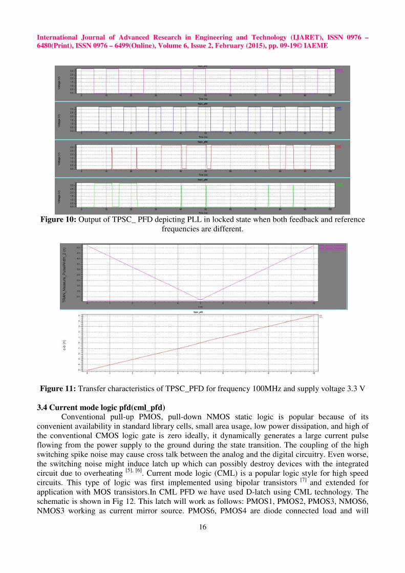
Figure 11: Transfer characteristics of TPSC_PFD for frequency 100MHz and supply voltage 3.3 V
3.4 Current mode logic pfd(cml_pfd)
Conventional pull-up PMOS, pull-down NMOS static logic is popular because of its
convenient availability in standard library cells, small area usage, low power dissipation, and high of
the conventional CMOS logic gate is zero ideally, it dynamically generates a large current pulse
flowing from the power supply to the ground during the state transition. The coupling of the high
switching spike noise may cause cross talk between the analog and the digital circuitry. Even worse,
the switching noise might induce latch up which can possibly destroy devices with the integrated
circuit due to overheating [5], [6]
. Current mode logic (CML) is a popular logic style for high speed
circuits. This type of logic was first implemented using bipolar transistors [7]
and extended for
application with MOS transistors.In CML PFD we have used D-latch using CML technology. The
schematic is shown in Fig 12. This latch will work as follows: PMOS1, PMOS2, PMOS3, NMOS6,
NMOS3 working as current mirror source. PMOS6, PMOS4 are diode connected load and will

International Journal of Advanced Research in Engineering and Technology (IJARET), ISSN 0976 –
6480(Print), ISSN 0976 – 6499(Online), Volume 6, Issue 2, February (2015), pp. 09-19© IAEME
17
remain in saturation region. D and D_BAR are given at NMOS2 and NMOS5 while CLK and
CLK_BAR at NMOS1 and NMOS7. NMOS6 and NMOS9 are used to provide ground path to
outputs when CLK_BAR signal is high. This will force the circuit to be in reset state.
Figure 12: Schematic of Current Mode Logic (CML) based DFF
Figure 13: Output of CML_PFD depicting PLL in locked state when both feedback and reference
frequencies are different, (lead/lag at different instants).

International Journal of Advanced Research in Engineering and Technology (IJARET), ISSN 0976 –
6480(Print), ISSN 0976 – 6499(Online), Volume 6, Issue 2, February (2015), pp. 09-19© IAEME
18
Figure 14: Transfer characteristics of CML_ PFD for frequency 100MHz and supply voltage 3.3
3.5 Simulations
The simulations mentioned above were done using Tanner tools 14 version. With the help of
S-EDIT, W-EDIT, L-EDIT net list was generated and SPICE commands were used to obtain various
parameters mentioned in the Table 1.
Table 1: Comparison of different schemes of PFD
4. CONCLUSIONS
Four designs of PFD successfully compared and implemented which are NAND gate based
standard phase frequency detectors, DCVSL_PFD, TSPC_PFD and CML based PFD. It was found
that the designed PFD using standard NAND gates consume 0.4mW power, PFD using DCVSL
logic consumes 1.6mW and the TSPC PFD consumes 2.9mW, the power supply of 3.3mW. The
delay in output obtained with CML logic is least i.e. 0.5ns. All the models are designed to be dead
zone free. The locking time of 10ns is obtained for the different designs with reference and input
frequencies equal and of value 100MHZ. The DCVSL design and TSPC design can be used for low
output noise with DCVSL output noise being least and equal to -118.98db. Table 1 depicts the
difference in values for various parameters of all the four design logics.
ACKNOWLEDGMENTS
I express my sincere gratitude to my mentor and advisor Mr. Bal Krishan who provided me
the opportunity to proceed the research work under his guidance. In addition to providing me with
guidance and support, I thank for his timely help figuring out the start point of the research and the
resources required for executing the same. I would like to thank Ms Garima Jain for her help and
Silicon Mentor for stimulating discussions that helped immensely in accomplishing the research
assignment.
S_PFD CML_PFD DCVSL_PFD TSPC_PFD
Power 0.4 mW 7.5 mW 1.6 mW 2.9 mW
Glitch Time 0.6 ns 0.08 ns 0.38 ns 0.16 ns
Glitch Period 10 ns 10 ns 10 ns 10 ns
Delay 1.2 ns 0.5 ns 0.64 ns 0.23 ns
Output Noise -119.29 db -142.16 db -118.98 db -120.75 db

International Journal of Advanced Research in Engineering and Technology (IJARET), ISSN 0976 –
6480(Print), ISSN 0976 – 6499(Online), Volume 6, Issue 2, February (2015), pp. 09-19© IAEME
19
REFERENCES
1. Abishek Mann, Amit Karalkar, Lili He, Morris Jones, “The Design of A Low-Power Low-Noise
Phase Lock Loop” IEEE international Synopsys, qulity electronic design”, 2010, pp.,528-531.
2. HWANG-CHERNG CHOW and NAN-LIANG YEH“A New Phase-Locked Loop with High
Speed PhaseFrequency Detector and Enhanced Lock-in”, Proceedings of the 10th WSEAS
International Conference on CIRCUITS, Vouliagmeni, Athens, Greece, July 10-12, 2006 (pp96-
101).
3. N. Kumar Babu, P. Sasibala, “Fast Low Power Frequency Synthesis Applications By Using A
Dcvsl Delay Cell”, International Journal of Electrical and Electronics Engineering (IJEEE), ISSN
(PRINT): 2231 – 5284, Volume-3, Issue-2, 2013.
4. Kan M. Chu and David L. Pulfrey, “A Comparison of CMOS Circuit Techniques: Differential
Cascode Voltage Switch Logic Versus Conventional Logic”, IEEE Journal of Solid-State
Circuits, Vol. Sc-22, No. 4, August 1987.
5. D. T. Comer, Introduction to Mixed Signal VLSI. New York: Array Publishing Co., 1994.
6. D. J. Allstot, G. Liang, and H. C. Yang, “Current-mode logic techniques for cmos mixed-mode
asics,” Proceedings of the 1991 IEEE Integrated Circuits Conference, vol. 49, no. 8, pp. 25.2/1–
25.2/4, May 1991.
7. P. Gray, P. Hurst, S. Lewis, and R. Meyer, Analysis and design of analog integrated circuits, 4th
ed. New York: John Wiley & Sons, 2000.
8. Wen-Chi Wu,C,h ih-Chien Huung, Chih-Hsiung Chang', Nui-Heng Tseng, “Low power CMOS
PLL for clock generator”, IEEE International synopsis on circuits and systems,2003,vol-1, pp.I-
633-I-636.
9. Won-Hyo Lee; Jun-dong Cho; Sung-Dae Lee, “A high speed and low power phase-frequency
detector and charge-pump,” Design Automation Conference, 1999. Proceedings of the ASP-
DAC’99. Asia and South Pacific, vol., no., pp.269,272 vol.1, 18-21 Jan 1999.
10. K. Arshak, O. Abubaker, and E. Jafer, “Design and Simulation Difference Types CMOS Phase
Frequency Detector for High Speed and Low Jitter PLL”, proceedings of 5th IEEE International
Caracas Conference on Devices, Circuits, and Systems, ominican Republic, Vol. 1, Nov.3-5,
pp.188-191, 2004.
11. Ismail, N.M.H. and Othman, M., “CMOS phase frequency detector for high speed applications,”
Microelectronics ICM), 2009 International Conference on, vol., no., pp.201,204, 19-22 Dec.
2009.
12. Behzad Razavi, ―Design of Analog CMOS Integrated Circuits, McGraw- Hall, 2010.
13. Dean Bannerjee, PLL Performance, Simulation & Design, Edition 5, Reprint 2010.
14. Behzad Razavi, Monolithic Phase-Locked Loops and Clock Recovery Circuits: Theory and
Design, IEEE PRESS.
15. Smt. Smita Singhai and Prof. Bharti Dewani, “PLL Based Shunt Active Harmonic Filter To
Compensate Multiple Non-Linear Loads” International journal of Electronics and
Communication Engineering &Technology (IJECET), Volume 4, Issue 2, 2013, pp. 198 - 205,
ISSN Print: 0976- 6464, ISSN Online: 0976 –6472.
16. J.Ravindrababu , Dr.E.V.Krishna Rao, “Performance Analysis and Comparison of Linear Multi-
User Detectors In Ds-Cdma System” International journal of Electronics and Communication
Engineering &Technology (IJECET), Volume 3, Issue 1, 2012, pp. 229 - 243, ISSN Print: 0976-
6464, ISSN Online: 0976 –6472.
17. Rajinder Tiwari, R. K. Singh, “A New Approach For Design of Cmos Based Cascode Current
Mirror For Asp Applications” International journal of Electronics and Communication
Engineering &Technology (IJECET), Volume 2, Issue 2, 2011, pp. 1 - 7, ISSN Print: 0976- 6464,
ISSN Online: 0976 –6472.