Embed Size (px)
Citation preview
[AK1541]
MS1043-E-05 1 2013/03
AK1541 20 to 600MHz Delta-Sigma Fractional-N Frequency Synthesizer
1. Overview
The AK1541 is a Delta-Sigma Fractional-N PLL (Phase Locked Loop) frequency synthesizer with a frequency switching
function, covering a wide range of frequencies from 20 to 600MHz. This product consists of an 18-bit Delta-Sigma
modulator, a low-noise phase frequency comparator, a highly accurate charge pump, a reference divider and a
dual-module prescaler (P/P+1).
An excellent PLL can be achieved by combining this synthesizer with the external loop filter and VCO (Voltage Controlled
Oscillator). The access to the registers is controlled via a three-lines serial interface. The operating supply voltage is from
2.7 to 5.5V; and the charge pump and serial interface can be driven by individual supply voltages.
2. Features
Delta-Sigma Fractional-N frequency synthesizer providing shorter lockup time, lower phase noise and low spurious
performance
Operating frequency: 20 to 600MHz
On-chip charge pump for fast lockup
Programmable charge pump current:
In a normal operating scheme, the charge pump current can
be set in 16 steps, in the range from 10.6 to 168.9uA.
In a fast lockup scheme, the charge pump current can be
set in 8 steps, in the range from 0.84 to 2.32mA.
Supply Voltage: 2.7 to 5.5 V (PVDD and CPVDD pins)
Separate power supply for the charge pump: PVDD to 5.5V (CPVDD pin)
On-chip power-saving features
On-chip PLL lock detect feature: Direct output to the PFD (Phase Frequency Detector) or digital
filtering output can be selected.
Very low consumption current: 3.4mA typ. (excluding a charge pump current)
Package: 24pin QFN (0.5mm pitch, 4mm 4mm 0.7mm)
Operating temperature: -40C° to 85C°
[AK1541]
MS1043-E-05 2 2013/03
Table of Contents
1. Overview ___________________________________________________________________________ 1
2. Features ___________________________________________________________________________ 1
3. Block Diagram ______________________________________________________________________ 3
4. Pin Functional Description ____________________________________________________________ 4
5. Absolute Maximum Ratings ___________________________________________________________ 6
6. Recommended Operating Range _______________________________________________________ 6
7. Electrical Characteristics ______________________________________________________________ 7
8. Block Functional Descriptions ________________________________________________________ 11
9. Register Map _______________________________________________________________________ 19
10. Register Functional Description _______________________________________________________ 20
11. IC Interface Schematic _______________________________________________________________ 26
12. Recommended Connection Schematic for Off-Chip Components ___________________________ 28
13. Power-up Sequence _________________________________________________________________ 30
14. Typical Evaluation Board Schematic ___________________________________________________ 32
15. Block Diagram by Power Supply _______________________________________________________ 33
16. Outer Dimensions ___________________________________________________________________ 34
17. Marking ___________________________________________________________________________ 35
In this specification (draft version), the following notations are used for specific signal and register names:
[Name]: Pin name
<Name>: Register group name (Address name)
Name: Register bit name
[AK1541]
MS1043-E-05 3 2013/03
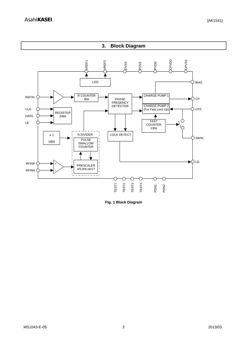
3. Block Diagram
CHARGE PUMP 2 (For Fast Lock Up)
CP
CPZ
PHASE
FREQENCY DETECTOR
REFIN
+
-
PRESCALER 4/5,8/9,16/17
PULSE SWALLOW COUNTER
LOCK DETECT
RFINP
RFINN
SWIN
CP
VD
D
CP
VS
S
PV
DD
VR
EF
2
VR
EF
1
DV
SS
PV
SS
LD
ΔΣ
18bit
CLK
DATA
LE
REGISTER
24bit
N DIVIDER
FAST COUNTER
13bit
PD
N1
TE
ST
2
TE
ST
1
LDO
TE
ST
3
PD
N2
TE
ST
4
R COUNTER 8bit
BIAS
CHARGE PUMP 1
Fig. 1 Block Diagram
[AK1541]
MS1043-E-05 4 2013/03
4. Pin Functional Description
Table 1 Pin Function
No. Name I/O Pin Functions Power down Remarks
1 CPVDD P Power supply for charge pump
2 TEST4 DI Test pin 4 Internal pull-down, Schmidt trigger input
3 TEST1 DI Test pin 1 Internal pull-down, Schmidt trigger input
4 LE DI Load enable Schmidt trigger input
5 DATA DI Serial data input Schmidt trigger input
6 CLK DI Serial clock Schmidt trigger input
7 LD DO Lock detect “Low”
8 PDN2 DI Power down pin for PLL Schmidt trigger input
9 PDN1 DI Power down signal for LDO Schmidt trigger input
10 REFIN AI Reference input
11 TEST2 DI Test pin 2 Internal pull-down, Schmidt trigger input
12 TEST3 DI Test pin 3 Internal pull-down, Schmidt trigger input
13 VREF1 AIO Connect to LDO reference voltage capacitor “Low”
14 DVSS G Digital ground pin
15 VREF2 AIO Connect to LDO reference voltage capacitor “Low”
16 RFINN AI Prescaler input
17 RFINP AI Prescaler input
18 PVDD P Power supply for peripherals
19 BIAS AIO Resistance pin for setting charge pump output current
20 PVSS G Ground pin for peripherals
21 CP AO Charge pump output “Hi-Z”
22 CPZ AIO Connect to the loop filter capacitor Notes 1) & 2)
23 SWIN AI Connect to resistance pin for fast lockup Notes 1) & 2)
24 CPVSS G Ground pin for charge pump
Note 1) For detailed functional descriptions, see the section “Charge Pump and Loop Filter” in “8. Block Functional
Description” below.
Note 2) The input voltage from the [CPZ] pin is used in the internal circuit. The [CPZ] pin must not be open even
when the fast lockup feature is unused. For the output destination from the [CPZ] pin, see “P.12 Fig.5 Loop

[AK1541]
MS1043-E-05 5 2013/03
Filter Schematic”. The [SWIN] pin could be open even when the first lockup feature is not used.
Note 3) Power down refers to the state where [PDN1]=[PDN2]=”Low” after power-on.
AI: Analog input pin AO: Analog output pin AIO: Analog I/O pin DI: Digital input pin
DO: Digital output pin P: Power supply pin G: Ground pin
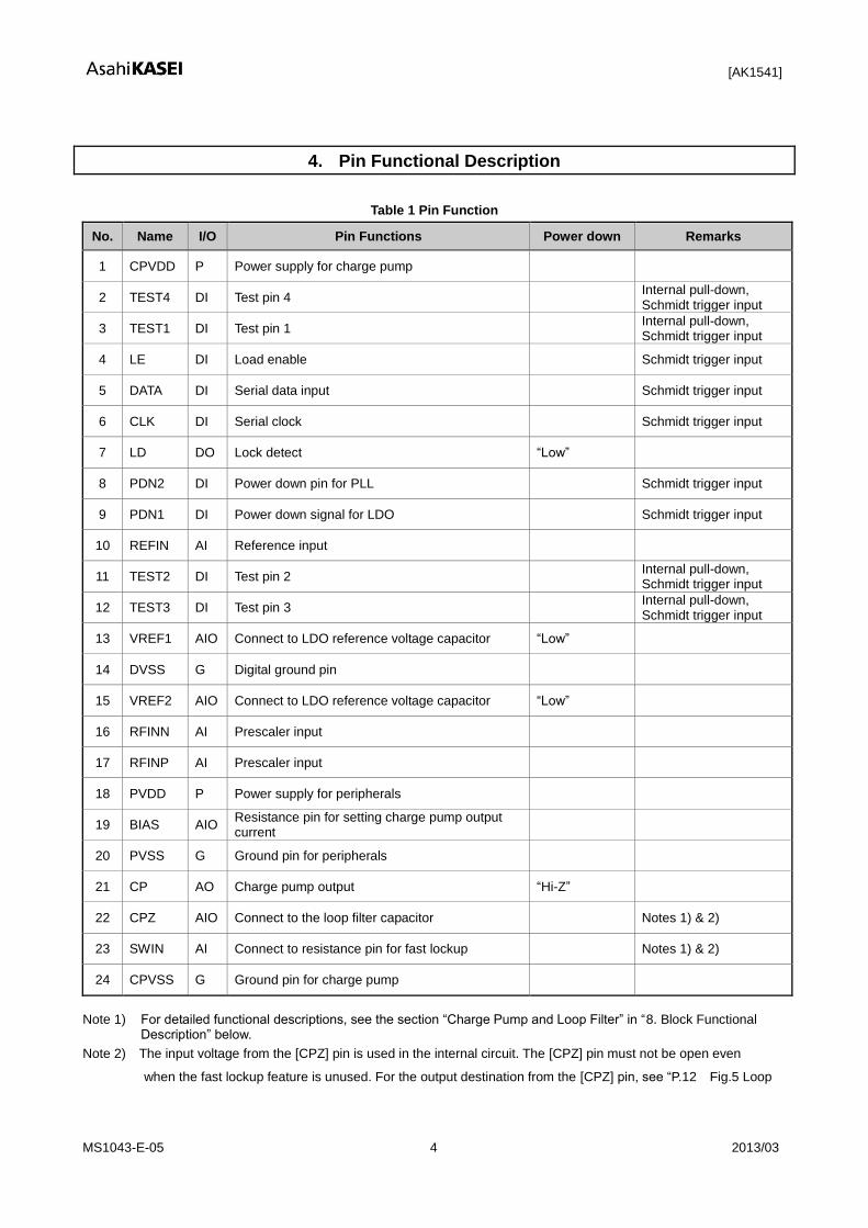
Fig. 2 Package Pin Layout
1
2
3
4
5
6
7 8 9 10
15
14
13
12 11
20 19
18
17
16 TOP
VIEW
23 24 22 21
CPVDD
TEST4
TEST1
DATA
LE
CLK
LD
PD
N2
PD
N1
RE
FIN
TE
ST
2
TE
ST
3
VREF1
DVSS
VREF2
RFINN
RFINP
PVDD
BIA
S
PV
SS
CP
CP
Z
SW
IN
CP
VS
S
[AK1541]
MS1043-E-05 6 2013/03
5. Absolute Maximum Ratings
Table 2 Absolute Maximum Ratings
Parameter Symbol Min. Max. Unit Remarks
Supply Voltage VDD1 -0.3 6.5 V Note 1) Applied to the [PVDD] pin
VDD2 -0.3 6.5 V Note 1) Applied to [CPVDD] pin
Ground Level
VSS1 0 0 V Voltage ground level applied to the [PVSS] pin
VSS2 0 0 V Voltage ground level applied to the [CPVSS] pin
VSS3 0 0 V Voltage ground level applied to the [DVSS] pin
Analog Input Voltage VAIN1 VSS1-0.3 VDD1+0.3 V Notes 1) & 2)
VAIN2 VSS2-0.3 VDD2+0.3 V Notes 1) & 3)
Digital Input Voltage VDIN VSS3-0.3 VDD1+0.3 V Notes 1) & 4)
Input Current IIN -10 10 mA
Storage Temperature Tstg -55 125 °C
Note 1) 0V reference for all voltages.
Note 2) Applied to the [ REFIN ], [ RFINN ] and [ RFINP ] pins.
Note 3) Applied to the [ CPZ ] and [ SWIN ] pins.
Note 4) Applied to the[ CLK ], [ DATA ], [ LE ], [ PDN1 ], [ PDN2 ], [ TEST1 ], [ TEST2 ], [ TEST3 ] and [ TEST4] pins.
Exceeding these maximum ratings may result in damage to the AK1541. Normal operation is not guaranteed at these
extremes.
6. Recommended Operating Range
Table 3 Recommended Operating Range
Parameter Symbol Min. Typ. Max. Unit Remarks
Operating Temperature Ta -40 85 C
Supply Voltage VDD1 2.7 3.3 5.5 V Applied to the [PVDD] pin
VDD2 VDD1 5.0 5.5 V Applied to the [CPVDD] pin
Note 1) VDD1 and VDD2 can be driven individually within the recommended operating range.
The specifications are applicable within the recommended operating range (supply voltage/operating temperature).
[AK1541]
MS1043-E-05 7 2013/03
7. Electrical Characteristics
1. Digital DC Characteristics
Table 4 Digital DC Characteristics
Parameter Symbol Conditions Min. Typ. Max. Unit Remarks
High level input voltage Vih 0.8VDD1 V Note 1)
Low level input voltage Vil 0.2VDD1 V Note 1)
High level input current 1 Iih1 Vih = VDD1=5.5V -1 1 µA Note 2)
High level input current 2 Iih2 Vih = VDD1=5.5V 27 55 110 µA Note 3)
Low level input current Iil Vil = 0V, VDD1=5.5V -1 1 µA Note 1)
High level output voltage Voh Ioh = -500A VDD1-0.4 V Note 4)
Low level output voltage Vol Iol = 500A 0.4 V Note 4)
Note 1) Applied to the [ CLK ], [ DATA ], [ LE ], [ PDN1 ], [ PDN2 ], [ TEST1 ], [ TEST2 ], [ TEST3 ] and [ TEST4 ] pins.
Note 2) Applied to the [ CLK ], [ DATA ], [ LE] , [ PDN1 ]and [ PDN2 ] pins.
Note 3) Applied to the [ TEST1 ], [ TEST2 ], [ TEST3 ] and [ TEST4 ] pins.
Note 4) Applied to the [ LD ] pin.
[AK1541]
MS1043-E-05 8 2013/03
2. Serial Interface Timing
<Write-In Timing>
Fig. 3 Serial Interface Timing
Table 5 Serial Interface Timing
Parameter Symbol Min. Typ. Max. Unit Remarks
Clock L level hold time Tcl 40 ns
Clock H level hold time Tch 40 ns
Clock setup time Tcsu 20 ns
Data setup time Tsu 20 ns
Data hold time Thd 20 ns
LE Setup Time Tlesu 20 ns
LE Pulse Width Tle 40 ns
Note 1) LE pin has to be set “Low” after register data setting completed. If LE pin keeps “High” with CLK operation, the
register may not be guaranteed proper setting.
Note 2) While LE pin is setting “Low”, 24 iteration clocks have to be set with CLK pin. If 25 or larger clocks are set, the
last 24 clocks synchronized data are valid.
LE (Input)
CLK (Input)
DATA (Input)
Tsu Thd
Tcsu
D19 D18 D0 A0 A1 A2 A3
Tch Tcl
Tlesu Tle
D19
[AK1541]
MS1043-E-05 9 2013/03
3. Analog Circuit Characteristics
The resistance of 27 kΩ is connected to the [BIAS] pin, VDD1=2.7 to 5.5V, VDD2=VDD1 to 5.5V, –40°C ≤ Ta ≤ 85°C
Parameter Min. Typ. Max. Unit Remarks
RF Characteristics
Input Sensitivity -15 +5 dBm Input frequency ≥ 100MHz
-5 +5 dBm 20MH ≤ Input frequency < 100MHz
Input Frequency 20 250 MHz Prescaler 4/5
20 600 MHz Prescaler 8/9,16/17
REFIN Characteristics
Input Sensitivity 0.4 2 Vpp
Input Frequency 5 40 MHz
Maximum Allowable Prescaler Output Frequency
75 MHz
Phase Detector
Phase Detector Frequency 3 MHz
Charge Pump
Charge Pump 1 Maximum Value 168.9 µA
Charge Pump 1 Minimum Value 10.6 µA
Charge Pump 2 Maximum Value 2.32 mA
Charge Pump 2 Minimum Value 0.84 mA
Icp TRI-STATE Leak Current 1 nA 0.5 ≤ Vcpo ≤ VDD2-0.5
Mismatch between Source and Sink Currents Note 1)
10 % Vcpo = VDD2/2, Ta = 25°C
Icp vs. Vcpo Note 2) 15 % 0.5 ≤ Vcpo ≤ VDD2-0.5, Ta = 25°C
Others
VREF1,2 Rise Time 50 µs
Current Consumption
IDD1 10 µA [PDN1]=“Low”, [PDN2]=”Low"
IDD2 3.4 5 mA
[PDN1]=”High”,[PDN2]=”High”
IDD for [PVDD]
IDD3 1.2 mA
[PDN1]=”High”,[PDN2]=”High”
IDD for [CPVDD]
Note 1) Mismatch between Source and Sink Currents: [(|Isink|-|Isource|)/(|Isink|+|Isource|)/2] × 100 [%]
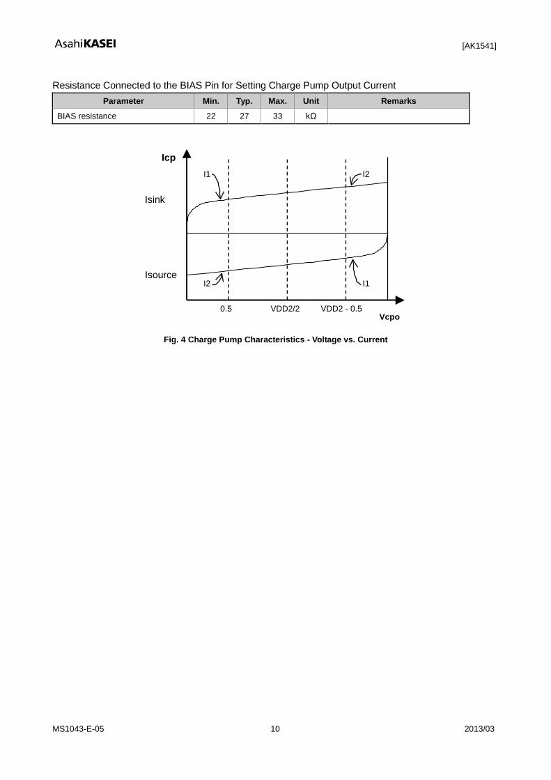
Note 2) See “Fig. 4 Charge Pump Characteristics - Voltage vs. Current”: Icp vs. Vcpo:
[1/2×(|I1|-|I2|)/1/2×(|I1|+|I2|)]×100 [%]
Note 3) [PDN1]=”High”, [PDN2]=”High” , the total current consumption = IDD2 + IDD3 + charge pump setting
Note 4) In the shipment test, the exposed pad on the center of the back of the package is connected to ground.
[AK1541]
MS1043-E-05 10 2013/03
Resistance Connected to the BIAS Pin for Setting Charge Pump Output Current
Parameter Min. Typ. Max. Unit Remarks
BIAS resistance 22 27 33 kΩ
Isink
Isource
Vcpo
Icp
VDD2 - 0.5 VDD2/2 0.5
I1
I1 I2
I2
Fig. 4 Charge Pump Characteristics - Voltage vs. Current
[AK1541]
MS1043-E-05 11 2013/03
8. Block Functional Descriptions
1. Frequency Setup
The AK1541 is a Fractional-N type synthesizer that takes 218
as the denominator, which calculates the integer and
numerator to be set using the following formulas:
Frequency setting = Ref Frequency x (Integer + Numerator / 218
)
Integer = ROUND (Target Frequency / FPFD)
Numerator = ROUND (Target Frequency – Integer x FPFD) / (FPFD / 218
)
Note) ROUND: Rounded off to the nearest value
FPFD : Phase Frequency Detector comparative Frequency([REFIN] pin input frequency/R divider ratio)
Calculation examples
Example 1) The numerator is positive when the target frequency is 465.0375MHz and the Phase Frequency Detector
comparative Frequency is 1MHz.
Integer = 465.0375MHz / 1MHz = 465.0375
It is rounded off to 465 (decimal) = 1d1 (hexadecimal) = 1 1101 0001 (binary)
Numerator = (465.0375MHz - 465 x 1MHz) / (1MHz / 218
) = 9830.4
It is rounded off to 9830 (decimal) = 2666 (hexadecimal) = 10 0110 0110 0110 (binary)
Frequency setting =1MHz x (465 + 9830 / 218
) = 465.0374985MHz
(In this case the error between the calculated frequency and the target frequency is 1.5Hz.)
Example 2) The numerator is negative when the target frequency is 468.550MHz and the Phase Frequency Detector
comparative Frequency is 1MHz.
Integer = 468.550MHz / 1MHz = 468.550
It is rounded off to 469 (decimal) = 1d5 (hexadecimal) = 1 1101 0101 (binary)
Numerator = (468.550MHz - 465 x 1MHz) / (1MHz / 218
) = -117964.8
It is rounded off to -117965 (decimal), which is deduced from 218
to be converted into binary for 2's complementary
expression.
218
- 117965 (decimal) = 144179 (decimal) = 23333 (hexadecimal) = 10 0011 0011 0011 0011 (binary)
Frequency setting =1MHz x (469 + (-117965/218
)) = 468.5499992MHz
(In this case the error between the calculated frequency and the target frequency is 0.8Hz.)
Calculation of 2’s complement representation
1) Positive number: Binary expression (Unmanipulated) exp. 100 (decimal) = 64 (hexadecimal) = 110 0100
(binary)
2) Negative number: 218
minus this number in binary expression exp. –100 (decimal)
218
- 100 = 262044 (decimal) = 3FF9C (hexadecimal) = 11 1111 1111 1001 1100 (binary)
[AK1541]
MS1043-E-05 12 2013/03
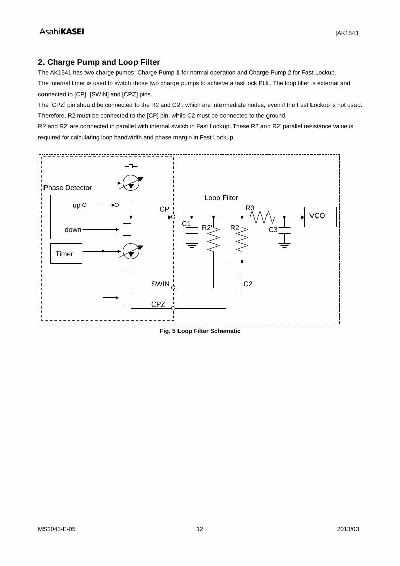
2. Charge Pump and Loop Filter
The AK1541 has two charge pumps; Charge Pump 1 for normal operation and Charge Pump 2 for Fast Lockup.
The internal timer is used to switch those two charge pumps to achieve a fast lock PLL. The loop filter is external and
connected to [CP], [SWIN] and [CPZ] pins.
The [CPZ] pin should be connected to the R2 and C2 , which are intermediate nodes, even if the Fast Lockup is not used.
Therefore, R2 must be connected to the [CP] pin, while C2 must be connected to the ground.
R2 and R2’ are connected in parallel with internal switch in Fast Lockup. These R2 and R2’ parallel resistance value is
required for calculating loop bandwidth and phase margin in Fast Lockup.
C2
Phase Detector
up
down
Timer
VCO
Loop Filter
C1 C3 R2 R2'
R3 CP
CPZ
SWIN
Fig. 5 Loop Filter Schematic
[AK1541]
MS1043-E-05 13 2013/03
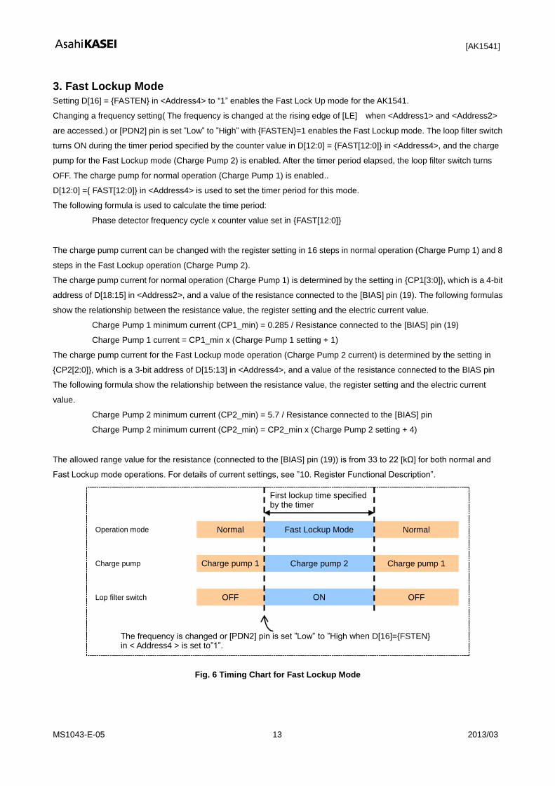
3. Fast Lockup Mode
Setting D[16] = FASTEN in <Address4> to “1” enables the Fast Lock Up mode for the AK1541.
Changing a frequency setting( The frequency is changed at the rising edge of [LE] when <Address1> and <Address2>
are accessed.) or [PDN2] pin is set ”Low” to ”High” with FASTEN=1 enables the Fast Lockup mode. The loop filter switch
turns ON during the timer period specified by the counter value in D[12:0] = FAST[12:0] in <Address4>, and the charge
pump for the Fast Lockup mode (Charge Pump 2) is enabled. After the timer period elapsed, the loop filter switch turns
OFF. The charge pump for normal operation (Charge Pump 1) is enabled..
D[12:0] = FAST[12:0] in <Address4> is used to set the timer period for this mode.
The following formula is used to calculate the time period:
Phase detector frequency cycle x counter value set in FAST[12:0]
The charge pump current can be changed with the register setting in 16 steps in normal operation (Charge Pump 1) and 8
steps in the Fast Lockup operation (Charge Pump 2).
The charge pump current for normal operation (Charge Pump 1) is determined by the setting in CP1[3:0], which is a 4-bit
address of D[18:15] in <Address2>, and a value of the resistance connected to the [BIAS] pin (19). The following formulas
show the relationship between the resistance value, the register setting and the electric current value.
Charge Pump 1 minimum current (CP1_min) = 0.285 / Resistance connected to the [BIAS] pin (19)
Charge Pump 1 current = CP1_min x (Charge Pump 1 setting + 1)
The charge pump current for the Fast Lockup mode operation (Charge Pump 2 current) is determined by the setting in
CP2[2:0], which is a 3-bit address of D[15:13] in <Address4>, and a value of the resistance connected to the BIAS pin
The following formula show the relationship between the resistance value, the register setting and the electric current
value.
Charge Pump 2 minimum current (CP2_min) = 5.7 / Resistance connected to the [BIAS] pin
Charge Pump 2 minimum current (CP2_min) = CP2_min x (Charge Pump 2 setting + 4)
The allowed range value for the resistance (connected to the [BIAS] pin (19)) is from 33 to 22 [kΩ] for both normal and
Fast Lockup mode operations. For details of current settings, see ”10. Register Functional Description”.
Fast Lockup Mode
Charge pump 2
ON
Normal Normal
Charge pump 1
OFF
Charge pump 1
OFF
First lockup time specified by the timer
Operation mode
Charge pump
Lop filter switch
The frequency is changed or [PDN2] pin is set ”Low” to ”High when D[16]=FSTEN in < Address4 > is set to”1”.
Fig. 6 Timing Chart for Fast Lockup Mode
[AK1541]
MS1043-E-05 14 2013/03
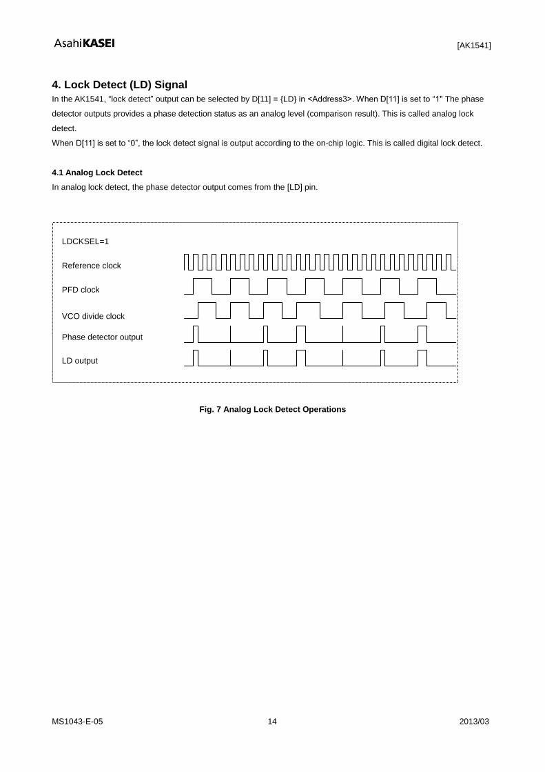
4. Lock Detect (LD) Signal
In the AK1541, “lock detect” output can be selected by D[11] = LD in <Address3>. When D[11] is set to “1" The phase
detector outputs provides a phase detection status as an analog level (comparison result). This is called analog lock
detect.
When D[11] is set to “0”, the lock detect signal is output according to the on-chip logic. This is called digital lock detect.
4.1 Analog Lock Detect
In analog lock detect, the phase detector output comes from the [LD] pin.
Fig. 7 Analog Lock Detect Operations
Reference clock
PFD clock
VCO divide clock
Phase detector output
LD output
LDCKSEL=1
[AK1541]
MS1043-E-05 15 2013/03
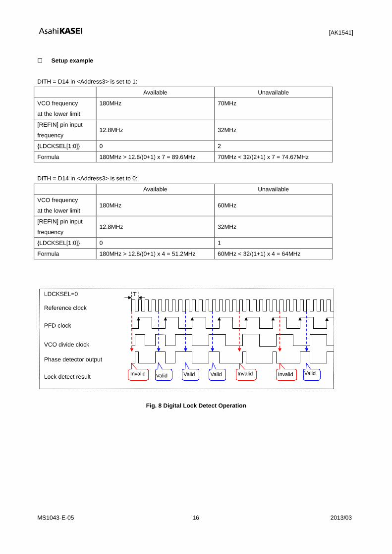
4.2 Digital Lock Detect
The accuracy of the phase detect is set by LDCKSEL[1:0].
LDCKSEL[1:0] is set to 0: T = REFIN cycle
LDCKSEL[1:0] is set to 1: T = REFIN cycle × 2 (This cannot be used for the reference dividing ratio ≤ 5.)
LDCKSEL[1:0] is set to 2: T = REFIN cycle × 3 (This cannot be used for the reference dividing ratio ≤ 6.)
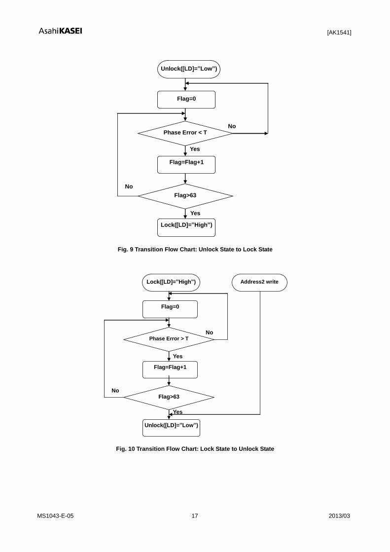
In the digital lock detect, the [LD] pin outputs is ”Low” every time when the frequency is set. And the [LD] pin outputs is
“High” (which means the locked state) when a phase error smaller than T is detected for 63 times consecutively. If the
phase error is larger than T is detected for N times consecutively then the [LD] pin outputs is “High” and then the [LD] pin
outputs is “Low”(which means the unlocked state).
Since the AK1541 is a Delta-Sigma Fractional-N type, a phase error up to 7 times larger than the VCO period frequency
may occur in the phase detector. Therefore the LDCKSEL[1:0] setting should be large enough to cover the amplitude
of the Delta-Sigma Fractional frequency. However, if the VCO frequency does not satisfy either of the following formula,
the digital lock detect cannot be used. In such case, the analog lock detect should be used.
DITH = D14 in <Address3> is set to 1: VCO frequency > [REFIN] pin input frequency / [LDCKSEL[1:0] setting + 1] x 7
DITH= D14 in <Address3> is set to 0: VCO frequency > [REFIN] pin input frequency / [LDCKSEL[1:0] setting + 1] x 4
Example 1)
If [REFIN] pin input frequency = 33.6MHz, DITH = 1, LDCKSEL[1:0] = 2,
33.6MHz / (2+1) x 7 = 78.4MHz
As a result, the digital lock detect cannot be used if the VCO frequency is equivalent to or smaller than 78.4MHz.
Example 2)
If [REFIN] pin input frequency = 33.6MHz, DITH = 0, LDCKSEL[1:0]= 1,
33.6MHz / (1+1) x 4 = 67.2MHz
As a result, the digital lock detect cannot be used if the VCO frequency is equivalent to or smaller than 67.2MHz.
[AK1541]
MS1043-E-05 16 2013/03
Setup example
DITH = D14 in <Address3> is set to 1:
Available Unavailable
VCO frequency
at the lower limit
180MHz 70MHz
[REFIN] pin input
frequency 12.8MHz 32MHz
LDCKSEL[1:0] 0 2
Formula 180MHz > 12.8/(0+1) x 7 = 89.6MHz 70MHz < 32/(2+1) x 7 = 74.67MHz
DITH = D14 in <Address3> is set to 0:
Available Unavailable
VCO frequency
at the lower limit 180MHz 60MHz
[REFIN] pin input
frequency 12.8MHz 32MHz
LDCKSEL[1:0] 0 1
Formula 180MHz > 12.8/(0+1) x 4 = 51.2MHz 60MHz < 32/(1+1) x 4 = 64MHz
Fig. 8 Digital Lock Detect Operation
Invalid
Invalid
Reference clock
PFD clock
VCO divide clock
Phase detector output
Valid
Valid Valid
Invalid
Valid
LDCKSEL=0 T
Lock detect result
[AK1541]
MS1043-E-05 17 2013/03
Phase Error < T
Flag=Flag+1
Lock([LD]=”High”)
Unlock([LD]=”Low”)
Yes
No
Flag>63
Flag=0
Yes
No
Fig. 9 Transition Flow Chart: Unlock State to Lock State
Phase Error > T
Yes
Flag=0
Flag=Flag+1
Flag>63 No
Yes
Unlock([LD]=”Low”)
No
Lock([LD]=”High”) Address2 write
Fig. 10 Transition Flow Chart: Lock State to Unlock State
[AK1541]
MS1043-E-05 18 2013/03
5. Reference Input
The reference input can be set with a dividing number in the range of 4 to 255 using R[7:0], which is a 8-bit address in
<Address3>. A dividing number from 0 to 3 cannot be set.
6. Prescaler and Swallow Counter
The dual modular prescaler (P/P + 1) and the swallow counter are used to provide a large dividing ratio.
The prescaler is set by PRE[1:0], which is a 2-bit address in <Address3>.
When PRE[1:0] =”00”, P = 4 is selected and then an integer from 89 to 8191 can be set.
When PRE[1:0] =”01”, P = 8 is selected and then an integer from 201 to 16383 can be set.
When PRE[1:0] =”10” or “11”, P = 16 is selected and then an integer from 521 to 32767 can be set.
For details of how to calculate an integer, see the section “Frequency Setup” in “8. Block Functional Description”.
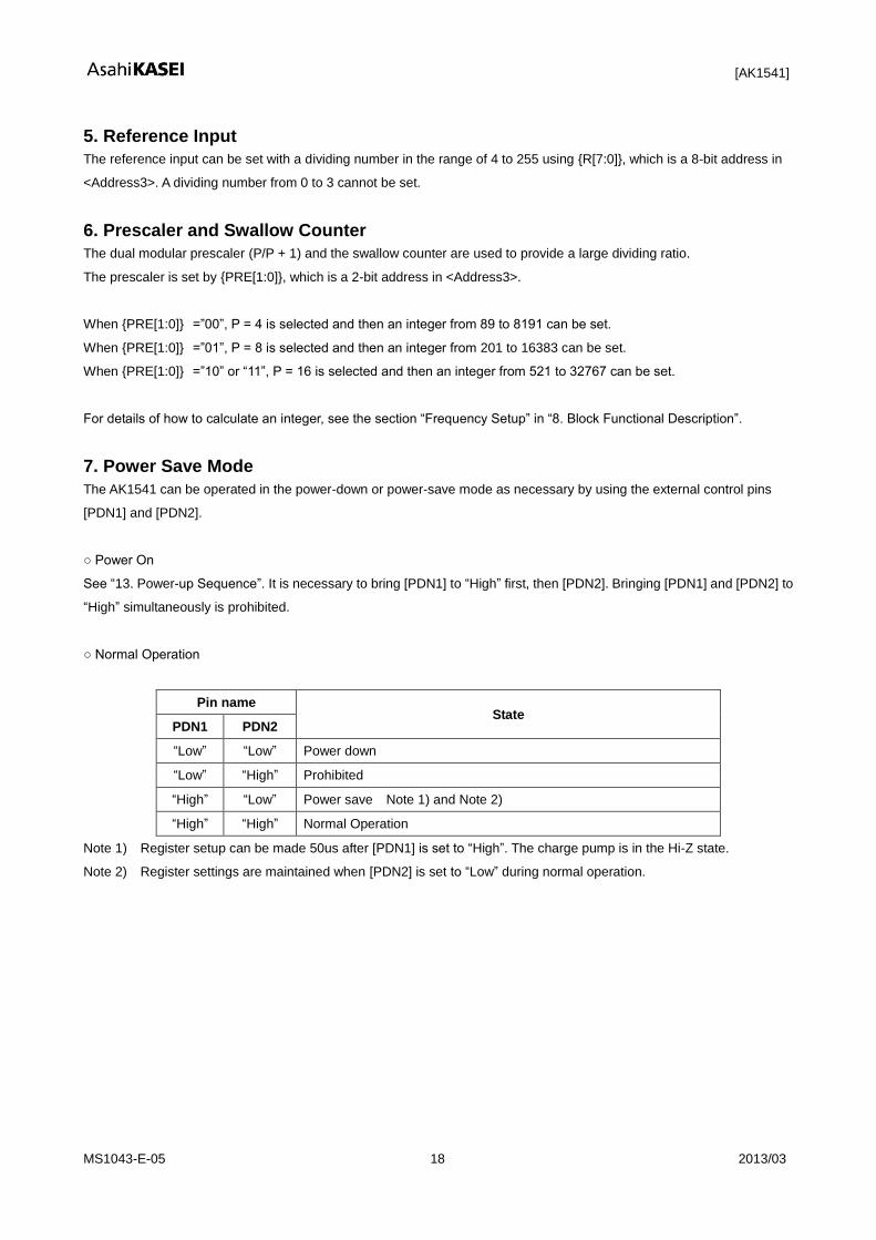
7. Power Save Mode
The AK1541 can be operated in the power-down or power-save mode as necessary by using the external control pins
[PDN1] and [PDN2].
Power On
See “13. Power-up Sequence”. It is necessary to bring [PDN1] to “High” first, then [PDN2]. Bringing [PDN1] and [PDN2] to
“High” simultaneously is prohibited.
Normal Operation
Pin name State
PDN1 PDN2
“Low” “Low” Power down
“Low” “High” Prohibited
“High” “Low” Power save Note 1) and Note 2)
“High” “High” Normal Operation
Note 1) Register setup can be made 50us after [PDN1] is set to “High”. The charge pump is in the Hi-Z state.
Note 2) Register settings are maintained when [PDN2] is set to “Low” during normal operation.
[AK1541]
MS1043-E-05 19 2013/03
9. Register Map
Name D19 D18 D17 D16 D15 D14 D13 D12 D11 D10 D9 D8 D7 D6 D5 D4 D3 D2 D1 D0 Address
Num 0 0 NUM [17]
NUM [16]
NUM [15]
NUM [14]
NUM [13]
NUM [12]
NUM [11]
NUM [10]
NUM [9]
NUM [8]
NUM [7]
NUM [6]
NUM [5]
NUM [4]
NUM [3]
NUM [2]
NUM [1]
NUM [0]
0x01
Int 0 CP1 [3]
CP1 [2]
CP1 [1]
CP1 [0]
INT [14]
INT [13]
INT [12]
INT [11]
INT [10]
INT [9]
INT [8]
INT [7]
INT [6]
INT [5]
INT [4]
INT [3]
INT [2]
INT [1]
INT [0]
0x02
Div 0 0 0 0 CP HiZ
DITH LDCK SEL[1]
LDCK SEL[0]
LD CP
POLA PRE [1]
PRE [0]
R [7]
R [6]
R [5]
R [4]
R [3]
R [2]
R [1]
R [0]
0x03
Cp_fast 0 0 0 FAST
EN CP2 [2]
CP2 [1]
CP2 [0]
FAST [12]
FAST [11]
FAST [10]
FAST [9]
FAST [8]
FAST [7]
FAST [6]
FAST [5]
FAST [4]
FAST [3]
FAST [2]
FAST [1]
FAST [0]
0x04
Note 1) Writing into address 0x01 is enabled when writing into address 0x02 is performed. Be sure to write into address
0x01 first and then address 0x02.
Note 2) The initial register values are not defined. Therefore, even after [PDN1] is set to “High”, each bit value remains
undefined. In order to set all register values, it is required to write the data in all addresses of the register.
Name Data Address
Num
D19 to D0
0 0 0 1
Int 0 0 1 0
Div 0 0 1 1
Cp_fast 0 1 0 0
[AK1541]
MS1043-E-05 20 2013/03
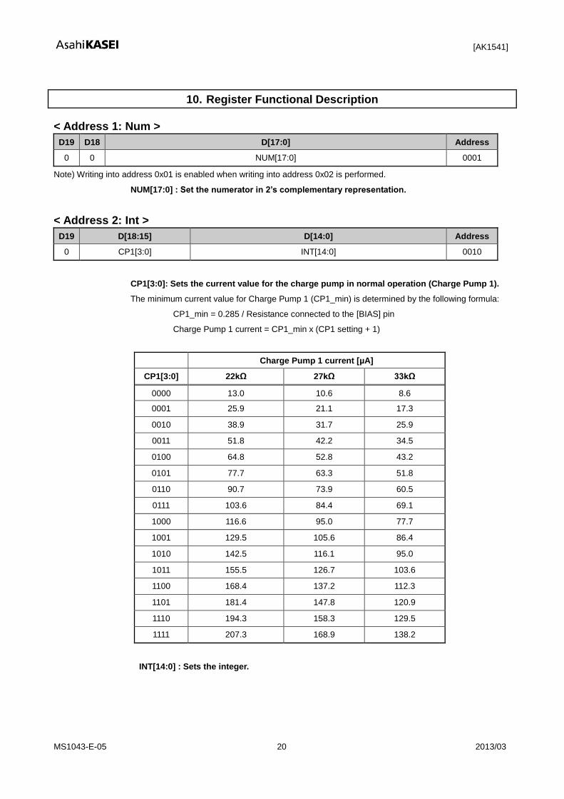
10. Register Functional Description
< Address 1: Num >
D19 D18 D[17:0] Address
0 0 NUM[17:0] 0001
Note) Writing into address 0x01 is enabled when writing into address 0x02 is performed.
NUM[17:0] : Set the numerator in 2’s complementary representation.
< Address 2: Int >
D19 D[18:15] D[14:0] Address
0 CP1[3:0] INT[14:0] 0010
CP1[3:0]: Sets the current value for the charge pump in normal operation (Charge Pump 1).
The minimum current value for Charge Pump 1 (CP1_min) is determined by the following formula:
CP1_min = 0.285 / Resistance connected to the [BIAS] pin
Charge Pump 1 current = CP1_min x (CP1 setting + 1)
Charge Pump 1 current [µA]
CP1[3:0] 22kΩ 27kΩ 33kΩ
0000 13.0 10.6 8.6
0001 25.9 21.1 17.3
0010 38.9 31.7 25.9
0011 51.8 42.2 34.5
0100 64.8 52.8 43.2
0101 77.7 63.3 51.8
0110 90.7 73.9 60.5
0111 103.6 84.4 69.1
1000 116.6 95.0 77.7
1001 129.5 105.6 86.4
1010 142.5 116.1 95.0
1011 155.5 126.7 103.6
1100 168.4 137.2 112.3
1101 181.4 147.8 120.9
1110 194.3 158.3 129.5
1111 207.3 168.9 138.2
INT[14:0] : Sets the integer.
[AK1541]
MS1043-E-05 21 2013/03
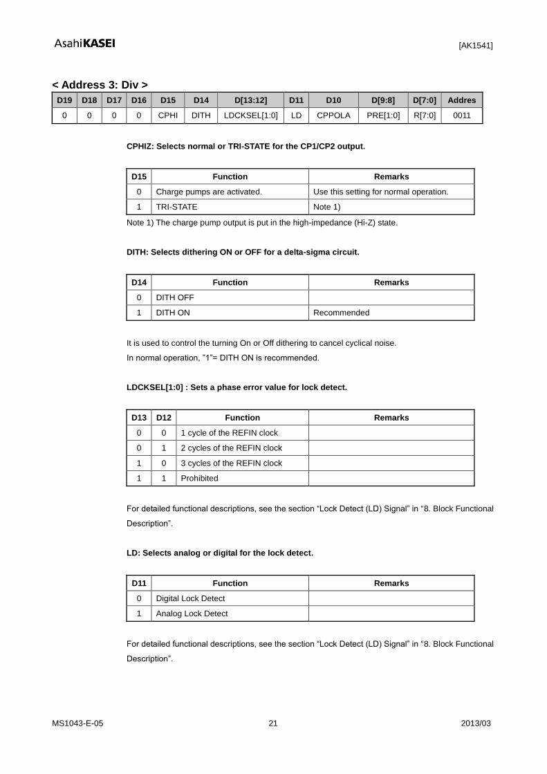
< Address 3: Div >
D19 D18 D17 D16 D15 D14 D[13:12] D11 D10 D[9:8] D[7:0] Addres
s 0 0 0 0 CPHI
Z
DITH LDCKSEL[1:0] LD CPPOLA PRE[1:0] R[7:0] 0011
CPHIZ: Selects normal or TRI-STATE for the CP1/CP2 output.
D15 Function Remarks
0 Charge pumps are activated. Use this setting for normal operation.
1 TRI-STATE Note 1)
Note 1) The charge pump output is put in the high-impedance (Hi-Z) state.
DITH: Selects dithering ON or OFF for a delta-sigma circuit.
D14 Function Remarks
0 DITH OFF
1 DITH ON Recommended
It is used to control the turning On or Off dithering to cancel cyclical noise.
In normal operation, ”1”= DITH ON is recommended.
LDCKSEL[1:0] : Sets a phase error value for lock detect.
D13 D12 Function Remarks
0 0 1 cycle of the REFIN clock
0 1 2 cycles of the REFIN clock
1 0 3 cycles of the REFIN clock
1 1 Prohibited
For detailed functional descriptions, see the section “Lock Detect (LD) Signal” in “8. Block Functional
Description”.
LD: Selects analog or digital for the lock detect.
D11 Function Remarks
0 Digital Lock Detect
1 Analog Lock Detect
For detailed functional descriptions, see the section “Lock Detect (LD) Signal” in “8. Block Functional
Description”.
[AK1541]
MS1043-E-05 22 2013/03
CPPOLA: Selects positive or negative output polarity for Charge Pump 1 and Charge Pump 2.
D10 Function Remarks
0 Positive
1 Negative
Fig. 11 Charge Pump slope Polarity
High
High
Charge pump output voltage
Negative
Positive
Low
Low
VC
O f
req
ue
nc
y

[AK1541]
MS1043-E-05 23 2013/03
PRE[1:0] : Selects a dividing ratio for the prescaler.
D9 D8 Function Remarks
0 0 P=4
0 1 P=8
1 0 P=16
1 1 P=16
R[7:0]: Sets a dividing ratio for the reference clock.
This can be set in the range from 4 (4 divisions) to 255 (255 divisions). 0, 1, 2 or 3 cannot be set.
D7 D6 D5 D4 D3 D2 D1 D0 Function Remarks
0 0 0 0 0 0 0 0 0 Prohibited
0 0 0 0 0 0 0 1 1 Prohibited
0 0 0 0 0 0 1 0 2 Prohibited
0 0 0 0 0 0 1 1 3 Prohibited
DATA
1 1 1 1 1 1 0 1 253
1 1 1 1 1 1 1 0 254
1 1 1 1 1 1 1 1 255
[AK1541]
MS1043-E-05 24 2013/03
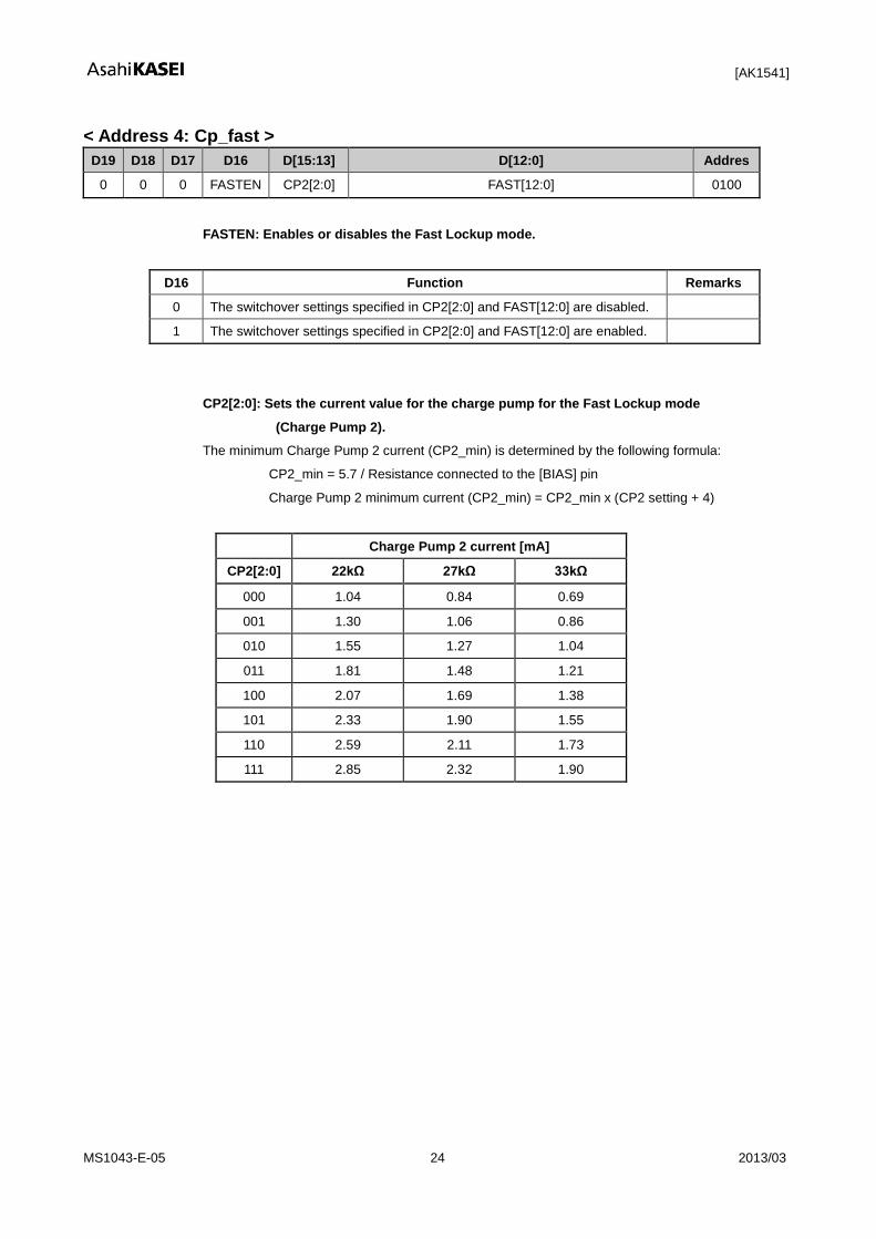
< Address 4: Cp_fast >
D19 D18 D17 D16 D[15:13] D[12:0] Addres
s 0 0 0 FASTEN CP2[2:0] FAST[12:0] 0100
FASTEN: Enables or disables the Fast Lockup mode.
D16 Function Remarks
0 The switchover settings specified in CP2[2:0] and FAST[12:0] are disabled.
1 The switchover settings specified in CP2[2:0] and FAST[12:0] are enabled.
CP2[2:0]: Sets the current value for the charge pump for the Fast Lockup mode
(Charge Pump 2).
The minimum Charge Pump 2 current (CP2_min) is determined by the following formula:
CP2_min = 5.7 / Resistance connected to the [BIAS] pin
Charge Pump 2 minimum current (CP2_min) = CP2_min x (CP2 setting + 4)
Charge Pump 2 current [mA]
CP2[2:0] 22kΩ 27kΩ 33kΩ
000 1.04 0.84 0.69
001 1.30 1.06 0.86
010 1.55 1.27 1.04
011 1.81 1.48 1.21
100 2.07 1.69 1.38
101 2.33 1.90 1.55
110 2.59 2.11 1.73
111 2.85 2.32 1.90
[AK1541]
MS1043-E-05 25 2013/03
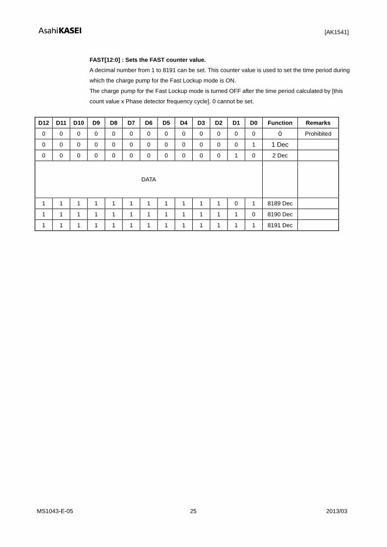
FAST[12:0] : Sets the FAST counter value.
A decimal number from 1 to 8191 can be set. This counter value is used to set the time period during
which the charge pump for the Fast Lockup mode is ON.
The charge pump for the Fast Lockup mode is turned OFF after the time period calculated by [this
count value x Phase detector frequency cycle]. 0 cannot be set.
D12 D11 D10 D9 D8 D7 D6 D5 D4 D3 D2 D1 D0 Function Remarks
0 0 0 0 0 0 0 0 0 0 0 0 0 0 Prohibited
0 0 0 0 0 0 0 0 0 0 0 0 1 1 Dec
0 0 0 0 0 0 0 0 0 0 0 1 0 2 Dec
DATA
1 1 1 1 1 1 1 1 1 1 1 0 1 8189 Dec
1 1 1 1 1 1 1 1 1 1 1 1 0 8190 Dec
1 1 1 1 1 1 1 1 1 1 1 1 1 8191 Dec
[AK1541]
MS1043-E-05 26 2013/03
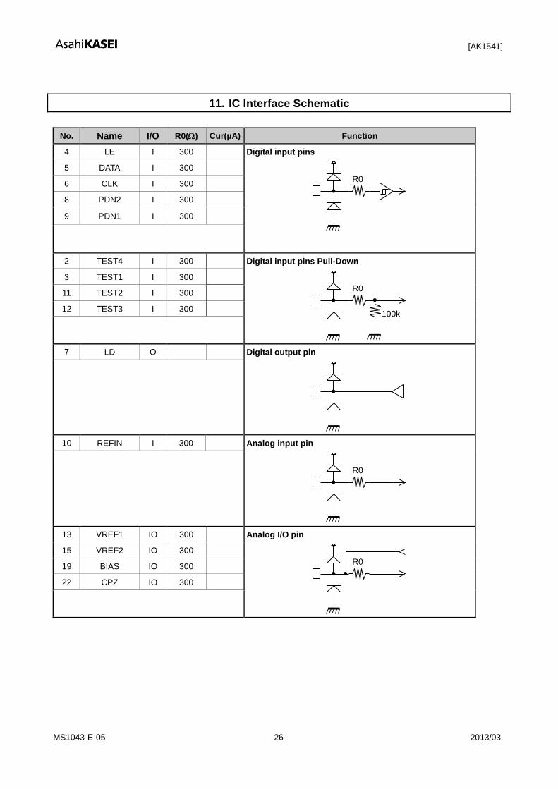
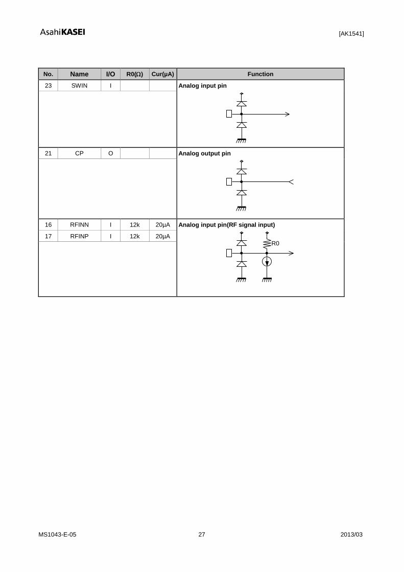
11. IC Interface Schematic
No. Name I/O R0() Cur(µA) Function
4 LE I 300 Digital input pins
R0
5 DATA I 300
6 CLK I 300
8 PDN2 I 300
9 PDN1 I 300
2 TEST4 I 300 Digital input pins Pull-Down
R0
100k
3 TEST1 I 300
11 TEST2 I 300
12 TEST3 I 300
7 LD O Digital output pin
10 REFIN I 300 Analog input pin
R0
13 VREF1 IO 300 Analog I/O pin
R0
15 VREF2 IO 300
19 BIAS IO 300
22 CPZ IO 300
[AK1541]
MS1043-E-05 27 2013/03
No. Name I/O R0() Cur(µA) Function
23 SWIN I Analog input pin
21 CP O Analog output pin
16 RFINN I 12k 20µA Analog input pin(RF signal input)
R0
17 RFINP I 12k 20µA
[AK1541]
MS1043-E-05 28 2013/03
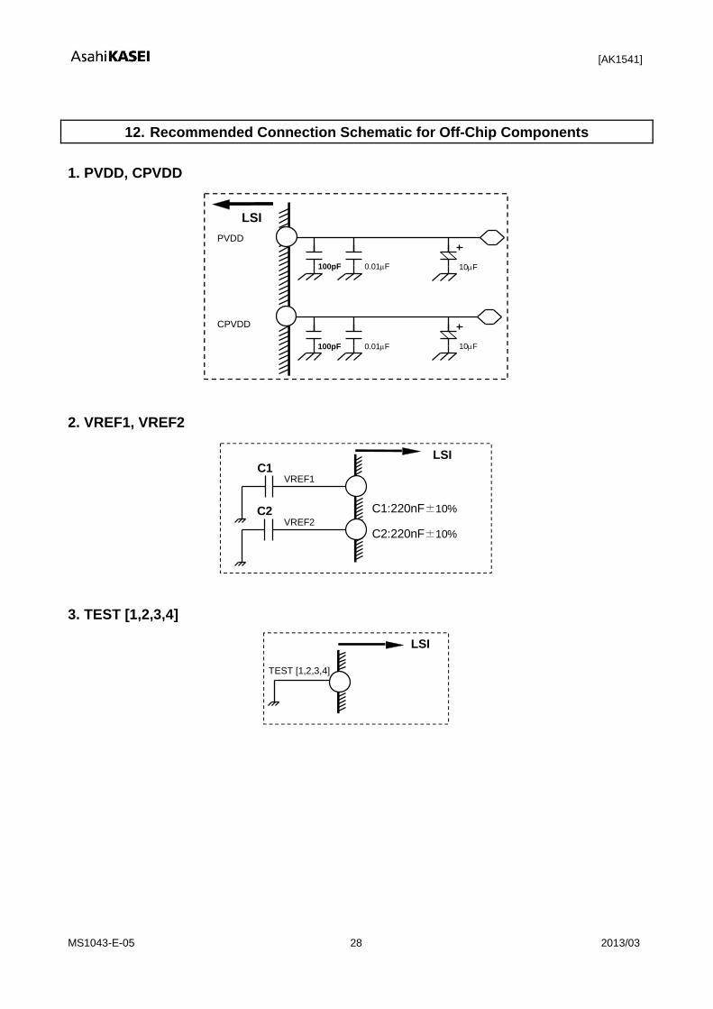
12. Recommended Connection Schematic for Off-Chip Components
1. PVDD, CPVDD
10F
PVDD
CPVDD
100pF
100pF 0.01F
10F
LSI
0.01F
2. VREF1, VREF2
C1 VREF1
VREF2
LSI
C1:220nF±10%
C2:220nF±10% VREF2
VREF2
C2
3. TEST [1,2,3,4]
TEST [1,2,3,4]
LSI
[AK1541]
MS1043-E-05 29 2013/03
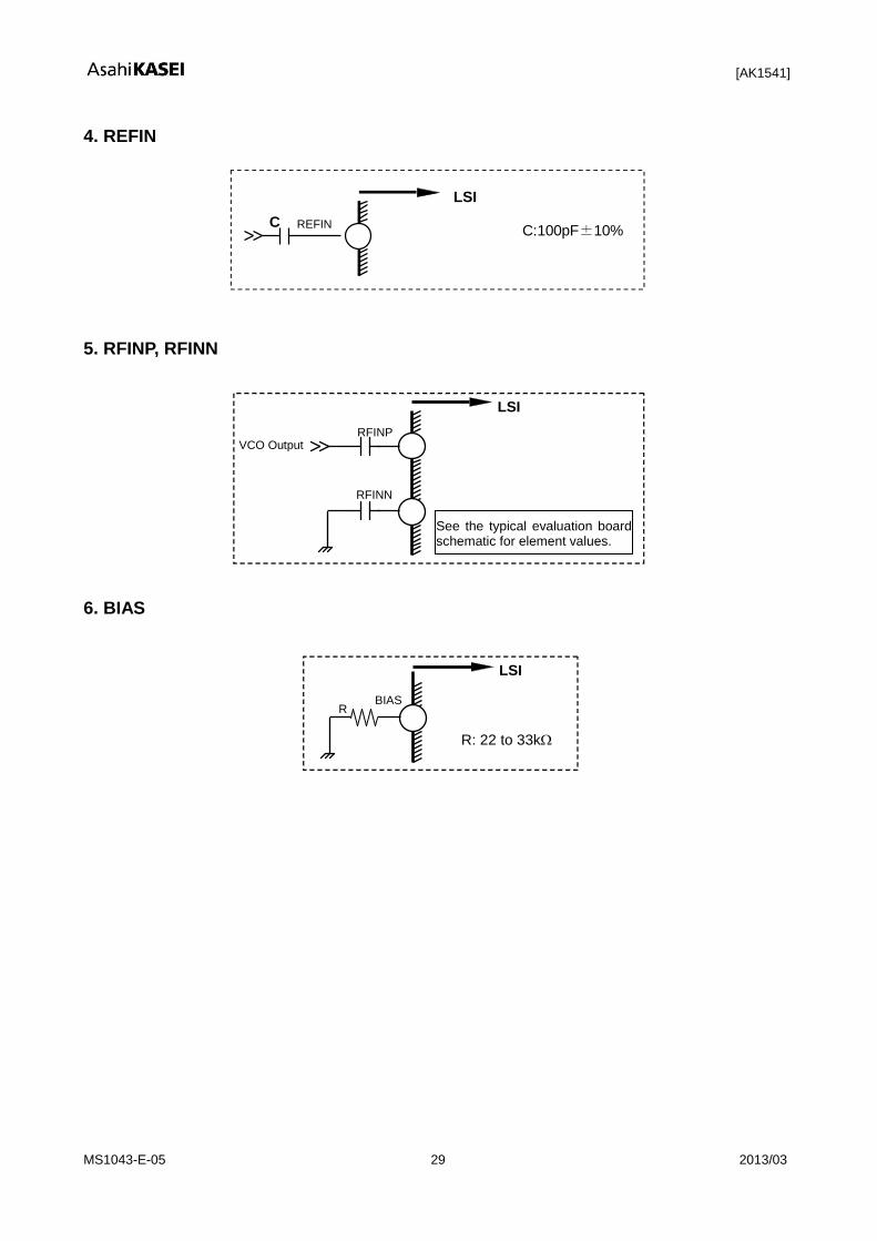
4. REFIN
REFIN C
LSI
C:100pF±10%
5. RFINP, RFINN
LSI
RFINP VCO Output
RFINN
See the typical evaluation board schematic for element values.
6. BIAS
LSI
BIAS
R: 22 to 33k
R
[AK1541]
MS1043-E-05 30 2013/03
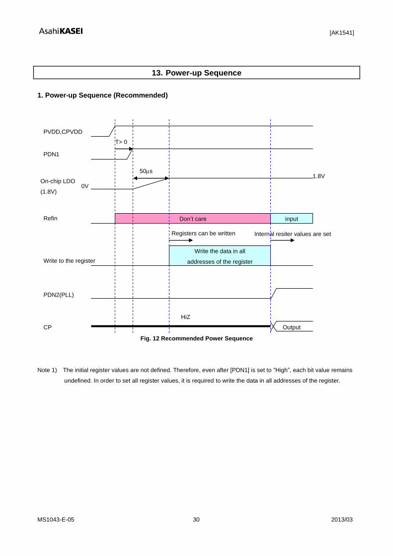
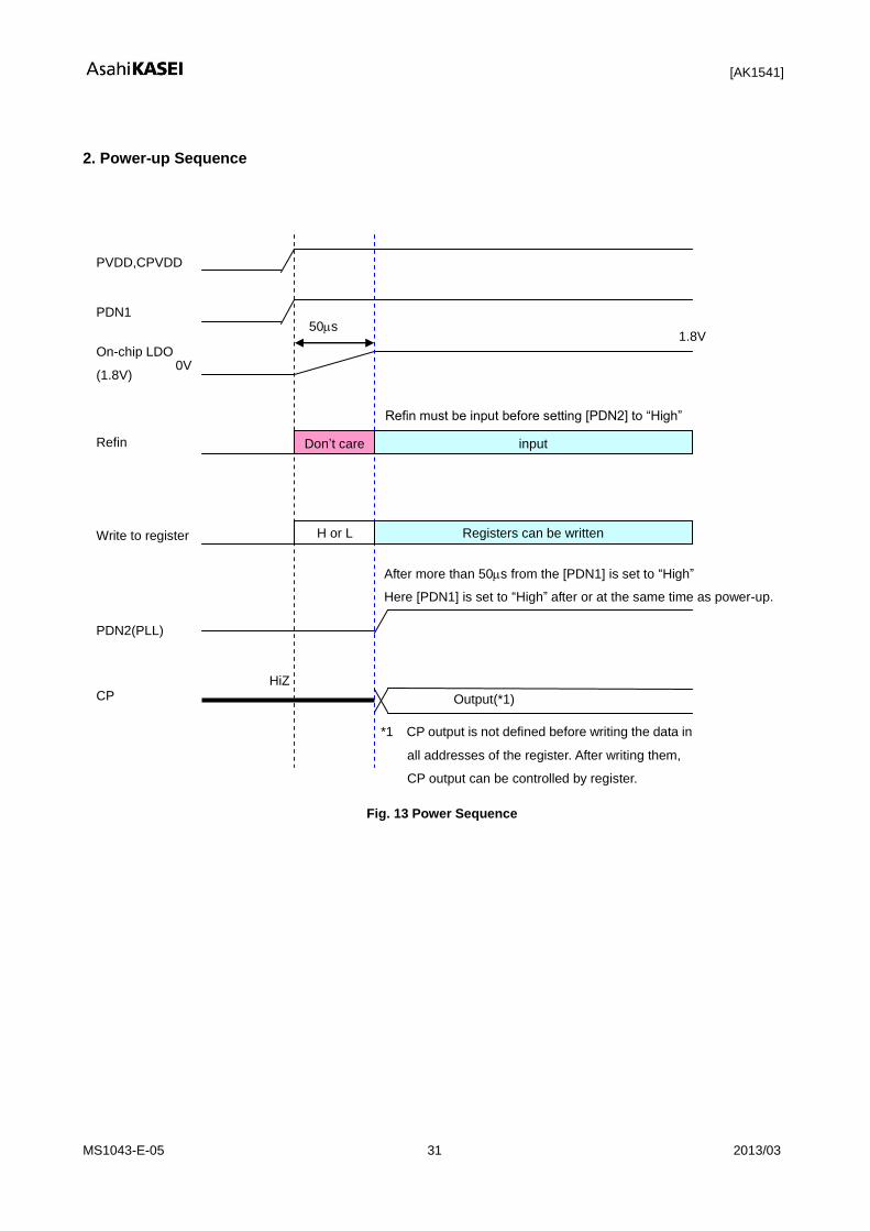
13. Power-up Sequence
1. Power-up Sequence (Recommended)
Fig. 12 Recommended Power Sequence
Note 1) The initial register values are not defined. Therefore, even after [PDN1] is set to “High”, each bit value remains
undefined. In order to set all register values, it is required to write the data in all addresses of the register.
PVDD,CPVDD
Write to the register
On-chip LDO
(1.8V)
PDN2(PLL)
Internal resiter values are set
CP Output
0V
1.8V 50s
HiZ
PDN1
T> 0
Refin Don’t care input
Registers can be written
Write the data in all
addresses of the register
[AK1541]
MS1043-E-05 31 2013/03
2. Power-up Sequence
Fig. 13 Power Sequence
PVDD,CPVDD
Write to register
On-chip LDO
(1.8V)
PDN2(PLL)
CP
0V
50s
HiZ
PDN1
Refin Don’t care input
Output(*1)
Registers can be written
After more than 50s from the [PDN1] is set to “High”
Here [PDN1] is set to “High” after or at the same time as power-up.
1.8V
Refin must be input before setting [PDN2] to “High”
*1 CP output is not defined before writing the data in
all addresses of the register. After writing them,
CP output can be controlled by register.
H or L
[AK1541]
MS1043-E-05 32 2013/03
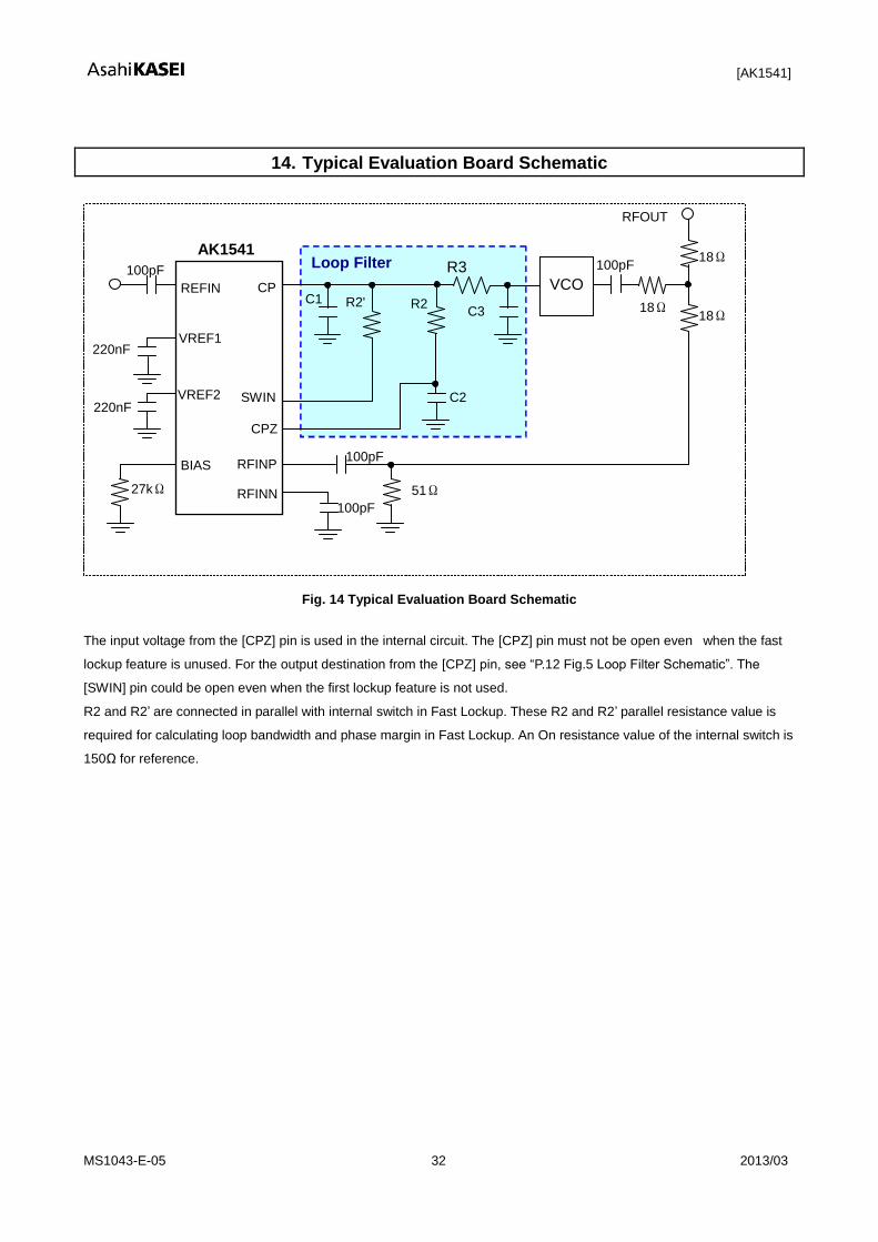
14. Typical Evaluation Board Schematic
C2
AK1541 Loop Filter
C1 C3
R2 R2'
R3
CP
CPZ
SWIN
RFOUT
51Ω
100pF
RFINN
VCO
BIAS RFINP
100pF
27kΩ
REFIN
VREF1
VREF2
220nF
220nF
100pF 100pF
18Ω
18Ω
18Ω
Fig. 14 Typical Evaluation Board Schematic
The input voltage from the [CPZ] pin is used in the internal circuit. The [CPZ] pin must not be open even when the fast
lockup feature is unused. For the output destination from the [CPZ] pin, see “P.12 Fig.5 Loop Filter Schematic”. The
[SWIN] pin could be open even when the first lockup feature is not used.
R2 and R2’ are connected in parallel with internal switch in Fast Lockup. These R2 and R2’ parallel resistance value is
required for calculating loop bandwidth and phase margin in Fast Lockup. An On resistance value of the internal switch is
150Ω for reference.

[AK1541]
MS1043-E-05 33 2013/03
15. Block Diagram by Power Supply
Fig. 15 Block Diagram by Power Supply

[AK1541]
MS1043-E-05 34 2013/03
16. Outer Dimensions
Fig. 16 Outer Dimensions
Note) It is recommended to connect the exposed pad (the center of the back of the package) to ground, although it will not
make any impact on the electrical characteristics if the pad is open.
0.05 S
2.40
2.4
0
0.4
0±0
.10
C0.30
1
13 18
19
24
12
7
4.0
0±0
.10
4.00±0.10
0.22±0.05
A
2.0
0
B
2.00
S
Part A
0.5
0.7
5M
AX
0.7
0
0.0
5M
AX
6
0.05 M S A B
0.0
0~
0.0
5
0.1
2~
0.1
8
0.17~0.27
Detailed chart in part A
[AK1541]
MS1043-E-05 35 2013/03
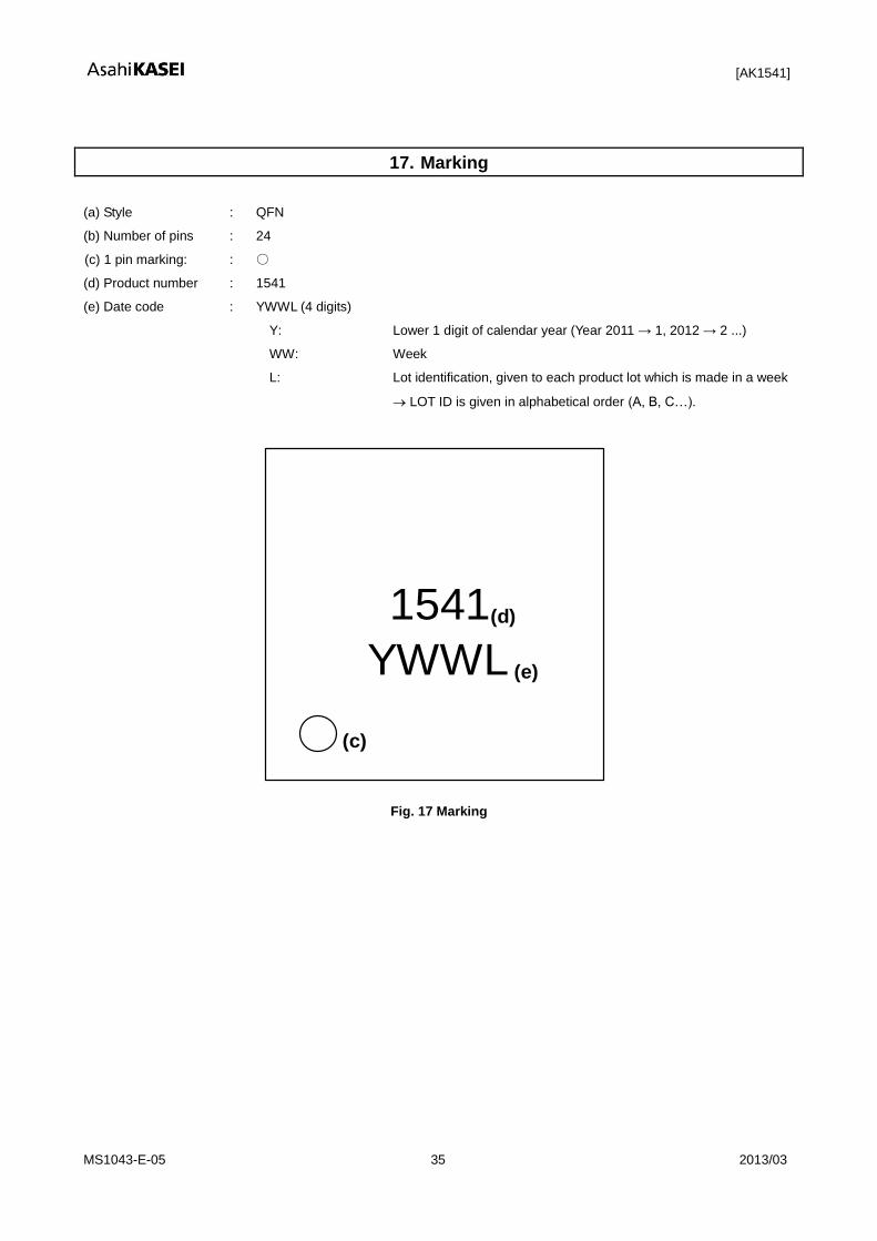
17. Marking
(a) Style : QFN
(b) Number of pins : 24
(c) 1 pin marking: :
(d) Product number : 1541
(e) Date code : YWWL (4 digits)
Y: Lower 1 digit of calendar year (Year 2011 → 1, 2012 → 2 ...)
WW: Week
L: Lot identification, given to each product lot which is made in a week
LOT ID is given in alphabetical order (A, B, C…).
YWWL (e)
(c)
1541(d)
Fig. 17 Marking
[AK1541]
MS1043-E-05 36 2013/03
IMPORTANT NOTICE These products and their specifications are subject to change without notice.
When you consider any use or application of these products, please make inquiries the sales office of Asahi Kasei Microdevices Corporation (AKM) or authorized distributors as to current status of the products.
Descriptions of external circuits, application circuits, software and other related information contained in this document are provided only to illustrate the operation and application examples of the semiconductor products. You are fully responsible for the incorporation of these external circuits, application circuits, software and other related information in the design of your equipments. AKM assumes no responsibility for any losses incurred by you or third parties arising from the use of these information herein. AKM assumes no liability for infringement of any patent, intellectual property, or other rights in the application or use of such information contained herein.
Any export of these products, or devices or systems containing them, may require an export license or other official approval under the law and regulations of the country of export pertaining to customs and tariffs, currency exchange, or strategic materials.
AKM products are neither intended nor authorized for use as critical componentsNote1) in any safety, life support, or other hazard related device or systemNote2), and AKM assumes no responsibility for such use, except for the use approved with the express written consent by Representative Director of AKM. As used here:
Note1) A critical component is one whose failure to function or perform may reasonably be expected to result, whether directly or indirectly, in the loss of the safety or effectiveness of the device or system containing it, and which must therefore meet very high standards of performance and reliability. Note2) A hazard related device or system is one designed or intended for life support or maintenance of safety or for applications in medicine, aerospace, nuclear energy, or other fields, in which its failure to function or perform may reasonably be expected to result in loss of life or in significant injury or damage to person or property.
It is the responsibility of the buyer or distributor of AKM products, who distributes, disposes of, or otherwise places the product with a third party, to notify such third party in advance of the above content and conditions, and the buyer or distributor agrees to assume any and all responsibility and liability for and hold AKM harmless from any and all claims arising from the use of said product in the absence of such notification.
2014/10
Related Parts
Part# Discription Comments
Mixer
AK1220 100MHz~900MHz High Linearity Down Conversion Mixer IIP3:+22dBm
AK1222 100MHz~900MHz Low Power Down Conversion Mixer IDD:2.9mA
AK1224 100MHz~900MHz Low Noise, High Liniarity Down Conversion Mixer NF:8.5dB, IIP3:+18dBm
AK1228 10MHz~2GHz Up/Down Conversion Mixer 3V Supply, NF:8.5dB
AK1221 0.7GHz~3.5GHz High Linearity Down Conversion Mixer IIP3:+25dBm
AK1223 3GHz~8.5GHz High Linearity Down Conversion Mixer IIP3:+13dB, NF:15dB
PLL Synthesizer
AK1541 20MHz~600MHz Low Power Fractional-N Synthesizer IDD:4.6mA
AK1542A 20MHz~600MHz Low Power Integer-N Synthesizer IDD:2.2mA
AK1543 400MHz~1.3GHz Low Power Fractional-N Synthesizer IDD:5.1mA
AK1544 400MHz~1.3GHz Low Power Integer-N Synthesizer IDD:2.8mA
AK1590 60MHz~1GHz Fractional-N Synthesizer IDD:2.5mA
AK1545 0.5GHz~3.5GHz Integer-N Synthesizer 16-TSSOP
AK1546 0.5GHz~3GHz Low Phase Noise Integer-N Synthesizer Normalized C/N:-226dBc/Hz
AK1547 0.5GHz~4GHz Integer-N Synthesizer 5V Supply
AK1548 1GHz~8GHz Low Phase Noise Integer-N Synthesizer Normalized C/N:-226dBc/Hz
IFVGA
AK1291 100~300MHz Analog Signal Control IF VGA w/ RSSI Dynamic Range:30dB
integrated VCO
AK1572 690MHz~4GHz Down Conversion Mixer with Frac.-N PLL and VCO IIP3:24dBm,
-111dBc/Hz@100kHz
AK1575 690MHz~4GHz Up Conversion Mixer with Frac.-N PLL and VCO IIP3:24dBm,
-111dBc/Hz@100kHz
IF Reciever (2nd Mixer + IF BPF + FM Detector)
AK2364 Built-in programmable AGC+BPF, FM detector IC IFBPF:10kHz ~ 4.5kHz
AK2365A Built-in programmable AGC+BPF, IFIC IFBPF:7.5kHz ~ 2kHz
Analog BB for PMR/LMR
AK2345C CTCSS Filter, Encoder, Decoder 24-VSOP
AK2360/
AK2360A Inverted frequency(3.376kHz/3.020kHz) scrambler 8-SON
AK2363 MSK Modem/DTMF Receiver 24-QFN
AK2346B 0.3-2.55/3.0kHz Analog audio filter,
Emphasis, Compandor, scrambler, MSK Modem
24-VSOP
AK2346A 24-QFN
AK2347B 0.3-2.55/3.0kHz Analog audio filter
Emphasis, Compandor, scrambler, CTCSS filter
24-VSOP
AK2347A 24-QFN
Function IC
AK2330 8-bit 8ch Electronic Volume VREF can be selected for each
channel
AK2331 8-bit 4ch Electronic Volume VREF can be selected for each
channel
Asahi Kasei Microdevices Corporation (“AKM”) reserves the right to make changes to the information contained in this document without
notice. When you consider any use or application of AKM product stipulated in this document, please make inquiries the sales office of
AKM or authorized distributors as to current status of the Products.
![AKD4425A-SA English Manual - Asahi Kasei Microdevices · AKD4425A-SA has a digital audio interface ... C24 (short) C29 2.2n R21 (short) + C28 (short) R16 470 J1 ... [Read] commands](https://img.pdfslide.net/doc/110x75/5b1b921a7f8b9a28258eb031/akd4425a-sa-english-manual-asahi-kasei-microdevices-akd4425a-sa-has-a-digital.jpg)
![AK2345 - AKM - Asahi Kasei Microdevices - Mixed Signal ... KASEI [AK2345] C0041-J-03 2006/09 - 3 - ブロック図 7 DREF 8 AMP4 Programmable OSC 22 23 RXIN DEM RXINO Splatter TSQLIM](https://img.pdfslide.net/doc/110x75/5ab1cf797f8b9ad9788cbe24/ak2345-akm-asahi-kasei-microdevices-mixed-signal-kasei-ak2345-c0041-j-03.jpg)
![AK2307 LV - AKM - Asahi Kasei Microdevices - Mixed ... KASEI [AK2307/LV] MS0199―J―04 2 2003/9 目次 項目 頁 l ブロック図 3 l パッケージ・ピン配置図 ..... 4](https://img.pdfslide.net/doc/110x75/5b2eb5ee7f8b9a594c8d8b1e/ak2307-lv-akm-asahi-kasei-microdevices-mixed-kasei-ak2307lv-ms0199j04.jpg)

![32-Bit 2ch DAC - AKM - Asahi Kasei Microdevices - Mixed ... · 32-Bit 2ch DAC [AK4490] MS1648-E-03 ... I2C PSN VREFHR VREFHR OUTRP VREFLR VR EFLR NC ... Connect at least 0.1uF or](https://img.pdfslide.net/doc/110x75/5afb91bd7f8b9a2d5d8fd3a9/32-bit-2ch-dac-akm-asahi-kasei-microdevices-mixed-2ch-dac-ak4490-ms1648-e-03.jpg)
![AK74xx series - AKM - Asahi Kasei Microdevices · [AK74xx_Shaft-End] ApplicationNote_MagnetSelection_Shaft-End-E-03 2019/10 - 3 - Diametral Magnet: A diametral magnetized magnet has](https://img.pdfslide.net/doc/110x75/60373bbc1e1a3751395aec43/ak74xx-series-akm-asahi-kasei-microdevices-ak74xxshaft-end-applicationnotemagnetselectionshaft-end-e-03.jpg)
![AK1228 - AKM - Asahi Kasei Microdevices - Mixed Signal ... · [AK1228] MS1535-E-02 2014/10 - 1 - AK 1. General Description AK1228 is a high linearity and low noise mixer. Signal input](https://img.pdfslide.net/doc/110x75/5c886cbc09d3f2224c8b9785/ak1228-akm-asahi-kasei-microdevices-mixed-signal-ak1228-ms1535-e-02.jpg)

![AK8975/AK8975C - AKM - Asahi Kasei Microdevices - …AK8975/C] AK8975/AK8975C 3-axis Electronic Compass 1. Features A 3-axis electronic compass IC with high sensitive Hall sensor technology](https://img.pdfslide.net/doc/110x75/5adf8edd7f8b9a8f298d1644/ak8975ak8975c-akm-asahi-kasei-microdevices-ak8975c-ak8975ak8975c-3-axis.jpg)
![USB 1A Li-ion IC - AKM - Asahi Kasei Microdevices ……¥力対応1A Li-ion バッテリーチャージャIC (充電アダプタ識別機能内蔵) AP4303 [AP4303] MS1497-J-00 - 2](https://img.pdfslide.net/doc/110x75/5ce2955088c99387408bcdc4/usb-1a-li-ion-ic-akm-asahi-kasei-microdevices-1a-li-ion-ic.jpg)
![AK09912 - AKM - Asahi Kasei Microdevices - Mixed …AK09912] MS1547-E-02 2014/7 - 6 - 4.3. Pin Function Pin No. Pin name I/O Power supply Type Function A1 DRDY O VID CMOS Data Ready](https://img.pdfslide.net/doc/110x75/5adf8edd7f8b9a8f298d1659/ak09912-akm-asahi-kasei-microdevices-mixed-ak09912-ms1547-e-02-20147.jpg)
![AK09911 - AKM - Asahi Kasei Microdevices - Mixed …AK09911] MS1526-E-01 2014/7 1--AK09911 3-axis Electronic Compass 1. Features A 3-axis electronic compass IC with high sensitive](https://img.pdfslide.net/doc/110x75/5b9e899f09d3f204248bf07e/ak09911-akm-asahi-kasei-microdevices-mixed-ak09911-ms1526-e-01-20147-1-ak09911.jpg)
![AK7401 English Datasheet - AKM - Asahi Kasei Microdevices · [AK7401] 014002685-E-01 2015/07 - 3 - SCLK 5. Functional Block Diagram HE-X INT(X) INT(Y) Rev. Vol. Protection Overvoltage](https://img.pdfslide.net/doc/110x75/5afc08667f8b9a32348fcc91/ak7401-english-datasheet-akm-asahi-kasei-microdevices-ak7401-014002685-e-01.jpg)


![AK5554 English Datasheet - VELVET SOUND - Asahi Kasei Microdevices (AKM) | AKM · 2020-05-07 · [AK5554] 015099864-E-00 2016/03 - 1 - 1. General Description The AK555x series is](https://img.pdfslide.net/doc/110x75/5f3898437aec725e745897e3/ak5554-english-datasheet-velvet-sound-asahi-kasei-microdevices-akm-akm-2020-05-07.jpg)