Embed Size (px)
Citation preview
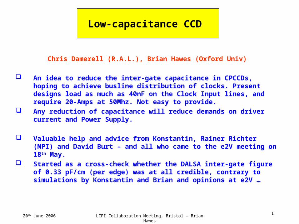
20th June 2006 LCFI Collaboration Meeting, Bristol – Brian Hawes1
Low-capacitance CCD
Chris Damerell (R.A.L.), Brian Hawes (Oxford Univ)
An idea to reduce the inter-gate capacitance in CPCCDs, hoping to achieve
busline distribution of clocks. Present designs load as much as 40nF on the Clock Input lines, and require 20-Amps at 50Mhz. Not easy to provide.
Any reduction of capacitance will reduce demands on driver current and Power Supply.
Valuable help and advice from Konstantin, Rainer Richter (MPI) and David Burt – and all who came to the e2V meeting on 18th May.
Started as a cross-check whether the DALSA inter-gate figure of 0.33 pF/cm (per edge) was at all credible, contrary to simulations by Konstantin and Brian and opinions at e2V …
20th June 2006 LCFI Collaboration Meeting, Bristol – Brian Hawes2
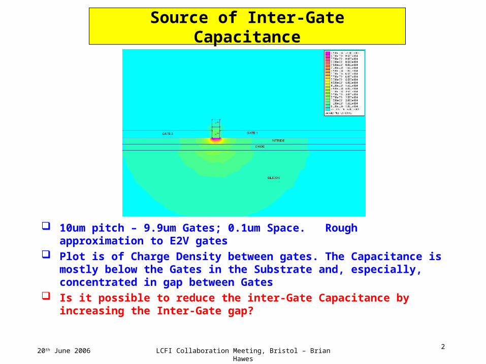
Source of Inter-Gate Capacitance
10um pitch – 9.9um Gates; 0.1um Space. Rough approximation to E2V gates
Plot is of Charge Density between gates. The Capacitance is mostly below the Gates in the Substrate and, especially, concentrated in gap between Gates
Is it possible to reduce the inter-Gate Capacitance by increasing the Inter-Gate gap?
20th June 2006 LCFI Collaboration Meeting, Bristol – Brian Hawes3
Effect of Increased Inter-Gate Gap
This was tried in 1996: the pnCCD architecture from MPI. The original design failed because the floating surface in the gaps caused major Charge Transfer problems.
The final version had the Inter-Gate strips metallised and biased. These are still working well.
Proposal for CPCCD’s (concept from Chris Damerell): Fabricate with raised Oxide Pedestals between reduced width Gates. These will will lift the necessary conducting surface above the level of the Gates and should further reduce the gate gap Capacitance.
20th June 2006 LCFI Collaboration Meeting, Bristol – Brian Hawes4
Simulation of Pedestal Gate Architecture [1]
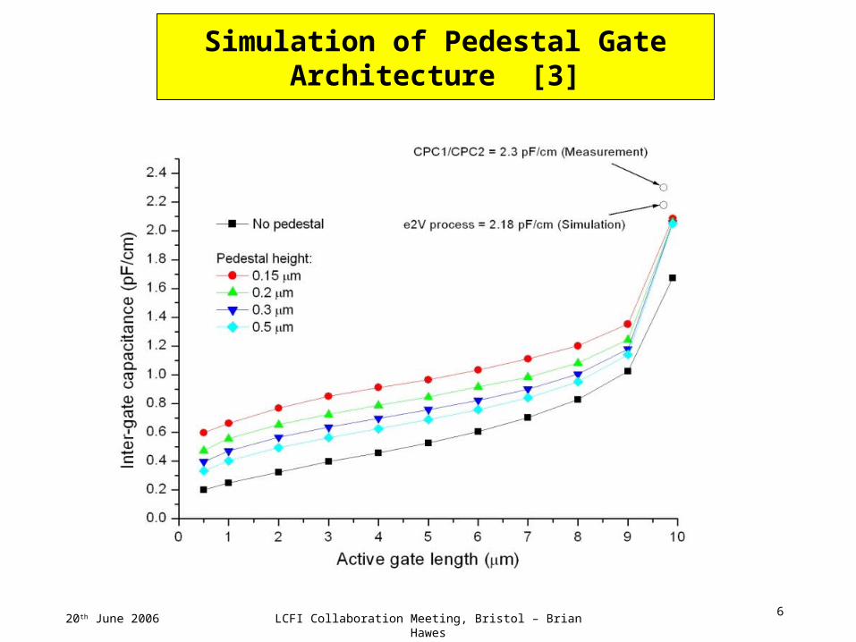
A series of simulations were run with active gate widths from 0.5 to 9.9 um, on 10um Gate pitch
For each gate width, the Pedestal height was varied from 0.15 to 0.5um
A ‘no pedestal’ case was also simulated, with free space between the gates.
There was no Oxide passivation over the structure in the simulations. This could have been added, but would not make a large difference.
20th June 2006 LCFI Collaboration Meeting, Bristol – Brian Hawes5
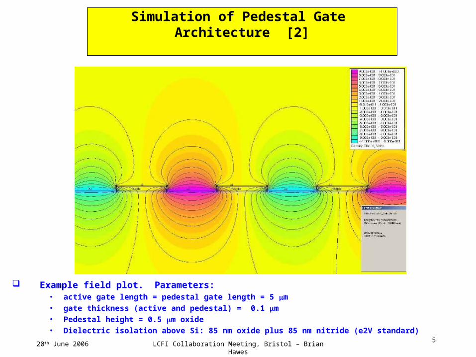
Example field plot. Parameters:
• active gate length = pedestal gate length = 5 m• gate thickness (active and pedestal) = 0.1 m• Pedestal height = 0.5 m oxide• Dielectric isolation above Si: 85 nm oxide plus 85 nm nitride (e2V standard)
Simulation of Pedestal Gate Architecture [2]
20th June 2006 LCFI Collaboration Meeting, Bristol – Brian Hawes6
Simulation of Pedestal Gate Architecture [3]
20th June 2006 LCFI Collaboration Meeting, Bristol – Brian Hawes7
Simulation of Pedestal Gate Architecture [4]
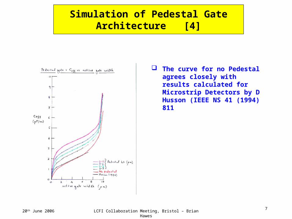
The curve for no Pedestal agrees closely with results calculated for Microstrip Detectors by D Husson (IEEE NS 41 (1994) 811
20th June 2006 LCFI Collaboration Meeting, Bristol – Brian Hawes8
Charge Distribution with profiled Gate surfaces [1]
20th June 2006 LCFI Collaboration Meeting, Bristol – Brian Hawes9
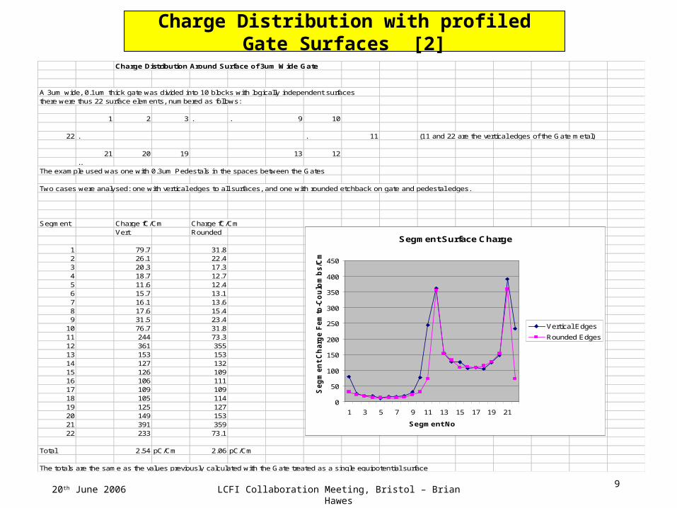
Charge Distribution with profiled Gate Surfaces [2]
Charge Distribution Around Surface of 3um Wide Gate
A 3um wide, 0.1um thick gate was divided into 10 blocks with logically independent surfacesthere were thus 22 surface elements, numbered as follows:
1 2 3 . . 9 10
22 . . 11 (11 and 22 are the vertical edges of the Gate metal)
21 20 19 13 12..
The example used was one with 0.3um Pedestals in the spaces between the Gates
Two cases were analysed: one with vertical edges to all surfaces, and one with rounded etchback on gate and pedestal edges.
Segment Charge fC/Cm Charge fC/CmVert Rounded
1 79.7 31.82 26.1 22.43 20.3 17.34 18.7 12.75 11.6 12.46 15.7 13.17 16.1 13.68 17.6 15.49 31.5 23.4
10 76.7 31.811 244 73.312 361 35513 153 15314 127 13215 126 10916 106 11117 109 10918 105 11419 125 12720 149 15321 391 35922 233 73.1
Total 2.54 pC/Cm 2.06 pC/Cm
The totals are the same as the values previously calculated with the Gate treated as a single equipotential surface
Segment Surface Charge
0
50
100
150
200
250
300
350
400
450
1 3 5 7 9 11 13 15 17 19 21
Segment No
Seg
men
t C
harg
e F
em
to-C
ou
lom
bs/C
mVertical Edges
Rounded Edges
20th June 2006 LCFI Collaboration Meeting, Bristol – Brian Hawes10
Summary of Results
2um Active Gates, and 0.5um high Pedestal gives 1.98 pF/cm, including capacitance to substrate. E2V process gives 8.82pF/cm.
This suggests Cg-g can be reduced by a factor 4 The Capacitance will be modified by true profile of gate edges, but
this effect is not large – perhaps a further 20% reduction.
The Capacitance simulations were performed using the FEMM4 program, by David Meeker (http://femm.foster-miller.net).
20th June 2006 LCFI Collaboration Meeting, Bristol – Brian Hawes11
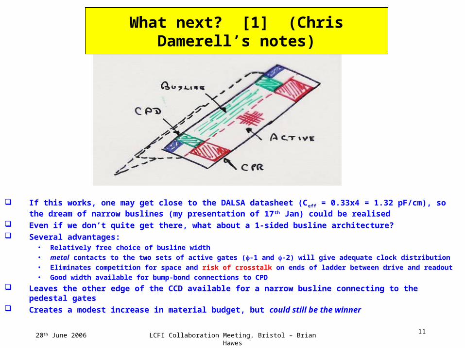
If this works, one may get close to the DALSA datasheet (Ceff = 0.33x4 = 1.32 pF/cm), so the dream
of narrow buslines (my presentation of 17th Jan) could be realised Even if we don’t quite get there, what about a 1-sided busline architecture? Several advantages:
• Relatively free choice of busline width• metal contacts to the two sets of active gates (-1 and -2) will give adequate clock distribution• Eliminates competition for space and risk of crosstalk on ends of ladder between drive and readout• Good width available for bump-bond connections to CPD
Leaves the other edge of the CCD available for a narrow busline connecting to the pedestal gates Creates a modest increase in material budget, but could still be the winner
What next? [1] (Chris Damerell’s notes)
20th June 2006 LCFI Collaboration Meeting, Bristol – Brian Hawes12
There are several possible showstoppers, even if such a structure can be made:
• Potential barriers or pockets at the transitions between active gates and pedestal gates
• Jitter in potential under the pedestal gate, due to fluctuations in phi-1 and phi-2 waveforms
• Radiation-induced shifts in this potential. However, if this is uniform across the device, it can be eliminated by adjusting the pedestal gate voltage
The possibility of greatly reduced CCD capacitance is of general interest. It has always been frustrating that transferring such small signal charges needed such high driver power
If it can be made to work, there could be wider applications
We have started to discuss possible test structures with e2V
We (Brian?) could extend the model outwards from the CCD, back through the buslines (how wide should they really be?) and through bump bonds back to the CPD output
What Next? [2]