Embed Size (px)
Citation preview
8/14/2019 2009_shrinky ndinks
http://slidepdf.com/reader/full/2009shrinky-ndinks 1/5
Tunable Nanowrinkles on Shape Memory Polymer Sheets
By Chi-Cheng Fu, Anthony Grimes, Maureen Long, Christopher G. L. Ferri,Brent D. Rich, Somnath Ghosh, Sayantani Ghosh, Luke P. Lee, Ajay Gopinathan,and Michelle Khine*
Researchers have long been fascinated by wrinkles as a pervasivenatural phenomenon. [1–4] Recently, there has been a resurgenceof interest in emulating and leveraging wrinkles for variousapplications. Polymeric wrinkles are nding increased utility ascomplex quasiperiodic structures important in applications,including cell-fate studies. [5,6] Flexible integrated circuits promis-ing many new applications, such as wearable systems, have beendemonstrated using thin buckled lms of single-crystallinesilicon based on elastomeric substrates. [7,8] Metal wrinkles, thinlms of metal on polymer substrates, have promise forapplications in molecular detection, optical devices, lters andsorters, high-surface-area conductors and actuators, and evenmetrology. [9–12] We have developed a rapid approach to createmetal nanowrinkles of tunable size and demonstrable utility on ashape memory polymer, [13,14] pre-stressed polystyrene (PS)sheetscommercially available as the children’s toy Shrinky-Dinks.
Previous demonstrations of wrinkles exhibited relatively largewrinkle wavelengths. For instance, Bowden et al. deposited metalonto a thermally expanded polydimethylsiloxane (PDMS) poly-
mer; the cooling of the PDMS causes a compressive stress, whichbuckles the deposited metal lm to achieve ca. 30 mmstructures. [9] Huck et al. augmented this approach withphotochemically patterned areas that differ in stiffness andthermal expansion. [15] Watanabe and Hirai more recently developed the very simple approach of simply pre-stretchingthe PDMS sheet to achieve 6–20 mm striped patterns. [16] Lacouret al. used this approach to create stretchable gold conductors. [11]
Yoo et al. imposed order on the buckling of polystyrene by applying a physical mold during the buckling process. [17] Whilethis group was able to achieve higher resolution wrinkles thanpreviously reported (down to 2 mm periodicity) as well asdirectionality, the process required a microfabricated mold andtook several hours.
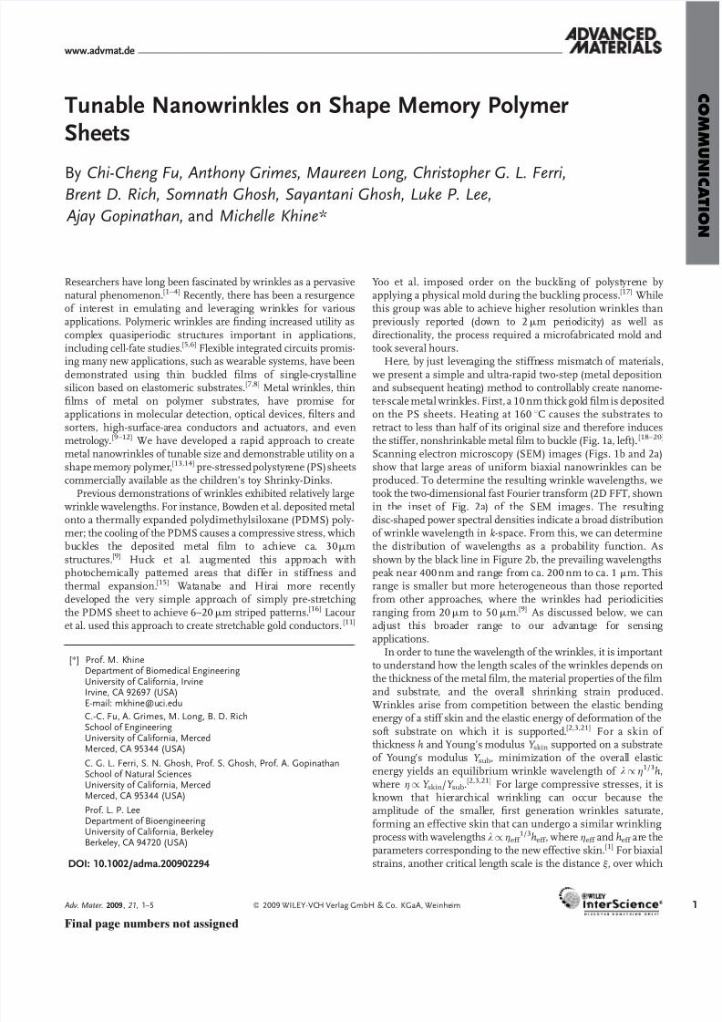
Here, by just leveraging the stiffness mismatch of materials,we present a simple and ultra-rapid two-step (metal depositionand subsequent heating) method to controllably create nanome-ter-scale metal wrinkles. First, a 10 nm thick gold lmis depositedon the PS sheets. Heating at 160 8 C causes the substrates toretract to less than half of its original size and therefore inducesthe stiffer, nonshrinkable metal lm to buckle (Fig. 1a, left). [18–20]
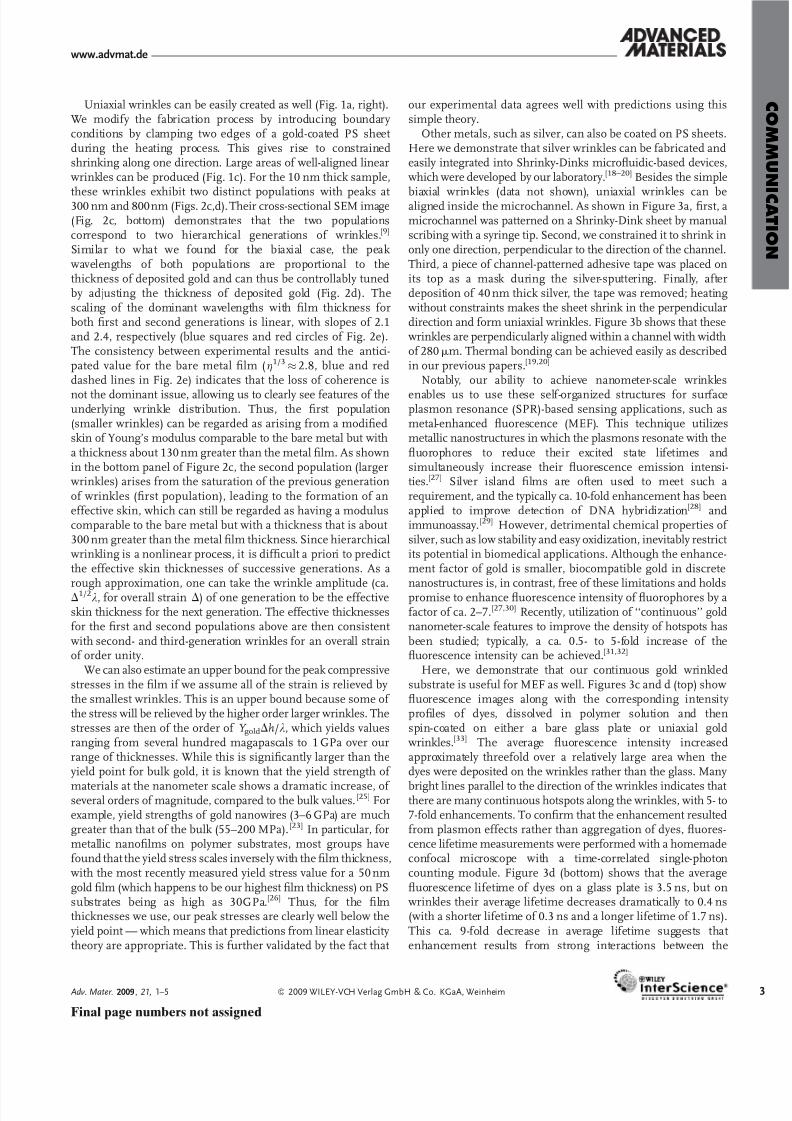
Scanning electron microscopy (SEM) images (Figs. 1b and 2a)show that large areas of uniform biaxial nanowrinkles can beproduced. To determine the resulting wrinkle wavelengths, wetook the two-dimensional fast Fourier transform (2D FFT, shownin the inset of Fig. 2a) of the SEM images. The resultingdisc-shaped power spectral densities indicate a broad distribution
of wrinkle wavelength ink-space. From this, we can determinethe distribution of wavelengths as a probability function. As
shown by the black line in Figure 2b, the prevailing wavelengthspeak near 400 nm and range from ca. 200 nm to ca. 1 mm. Thisrange is smaller but more heterogeneous than those reportedfrom other approaches, where the wrinkles had periodicitiesranging from 20 mm to 50 mm. [9] As discussed below, we canadjust this broader range to our advantage for sensingapplications.
In order to tune the wavelength of the wrinkles, it is important to understand how the length scales of the wrinkles depends onthe thickness of the metal lm, the material properties of the lmand substrate, and the overall shrinking strain produced.Wrinkles arise from competition between the elastic bendingenergy of a stiff skin and the elastic energy of deformation of thesoft substrate on which it is supported. [2,3,21] For a skin of thickness h and Young’s modulus Y skin supported on a substrateof Young’s modulus Y sub , minimization of the overall elasticenergy yields an equilibrium wrinkle wavelength of l / h1/3 h ,where h / Y skin / Y sub .[2,3,21] For large compressive stresses, it isknown that hierarchical wrinkling can occur because theamplitude of the smaller, rst generation wrinkles saturate,forming an effective skin that can undergo a similar wrinklingprocess with wavelengths l / heff
1/3 h eff , where heff and h eff are theparameters corresponding to the new effective skin. [1] For biaxialstrains, another critical length scale is the distance j , over which
www.advmat.de
[* ] Prof. M. KhineDepartment of Biomedical EngineeringUniversity of California, IrvineIrvine, CA 92697 (USA)E-mail: [email protected]
C.-C. Fu, A. Grimes, M. Long, B. D. RichSchool of EngineeringUniversity of California, MercedMerced, CA 95344 (USA)C. G. L. Ferri, S. N. Ghosh, Prof. S. Ghosh, Prof. A. GopinathanSchool of Natural SciencesUniversity of California, MercedMerced, CA 95344 (USA)Prof. L. P. LeeDepartment of BioengineeringUniversity of California, BerkeleyBerkeley, CA 94720 (USA)
DOI: 10.1002/adma.200902294
Adv. Mater. 2009 , 21, 1–5 ß 2009 WILEY-VCH Verlag GmbH & Co. KGaA, Weinheim 1
Final page numbers not assigned

8/14/2019 2009_shrinky ndinks
http://slidepdf.com/reader/full/2009shrinky-ndinks 2/5
COMMUNICATION
www.advmat.de
wrinkles lose orientational coherence. It scales as j / h2/3 h .[22] Forour case, a gold lm (Y gold % 78GPa) on a PS substrate
(Y PS % 3.5 GPa), we anticipate h ¼ Y gold / Y PS % 22.3.[23,24]
To verify the theoretical predictions, we varied the thickness of deposited gold from 10nm to 50nm. This caused a shift of hundreds of nanometers in the wavelength distributions(Fig. 2b). The experimental scaling of the peak wavelength withlm thickness (the black triangles of Fig. 2e) has a slope of 8.4,which agrees well with our theorized slope for the scaling of thecoherence length h2/3 % 7.9 (the black dashed line of Fig. 2e). Thissuggests that a loss of coherence is the dominant effect indetermining the morphology in the biaxial case. It should benoted, however, that there is an offset, indicating a modied skinapproximately 30 nm thicker than the bare metal lm and with a
comparable modulus. The occurrence of such modied lms hasbeen reported previously [9] and is a likely consequence of the
penetration of the metal into the substrate during theheat-shrinking process. Heating at 160 8 C, above the glasstransition temperature (95 8 C) and below the melting tempera-ture (240 8 C) of PS, induces the substrate to become soft enoughto be integrated into the wrinkling metal. [24] This phenomenondramatically increases the binding strength between gold and PSand thus changes the durability of the wrinkles, as conrmed by our empirical measurements and SEM analyses. Compared witha atgold lm(lm deposited after shrinking processbut heated),which can be easily removed, wrinkles are considerably strongerand can even bear ultrasonic cleaning over 5 min (data not shown).
Figure 1. Fabrication of nanowrinkles. a) Scheme of fabrication of biaxial(left) and uniaxial (right) wrinkles. b,c) SEM images of biaxial (b) anduniaxial (c) wrinkles on shrunk polystyrene sheets covered with a 10 nmthick layer of gold.
Figure 2. Characterization of nanowrinkles. a) SEM image of biaxial
wrinkles with 10nm thick gold. Inset: Its 2D FFT pattern. b) Wavelengthdistributions of biaxial wrinkles with various thickness of gold. c) Mainpanel: SEM image of uniaxial wrinkles with 10 nm thick gold. Inset: Its 2DFFT pattern. Bottom panel: Cross-sectional SEM view. d) Wavelengthdistributions of uniaxial wrinkles with various thickness of gold. e) Plotof main wavelength of biaxial (black triangles) and uniaxial (red circles andblue squares) wrinkles as a function of gold layer thickness. The dashedlines show anticipated slopes from the theory. Note that ‘‘1’’ and ‘‘2’’ in(c), (d), and (e) indicate the rst and the second populations of uniaxialwrinkle wavelengths.
ß 2009 WILEY-VCH Verlag GmbH & Co. KGaA, Weinheim Adv. Mater. 2009, 21, 1–5
Final page numbers not assigned
8/14/2019 2009_shrinky ndinks
http://slidepdf.com/reader/full/2009shrinky-ndinks 3/5
www.advmat.de
Uniaxial wrinkles can be easily created as well (Fig. 1a, right).We modify the fabrication process by introducing boundary conditions by clamping two edges of a gold-coated PS sheet during the heating process. This gives rise to constrainedshrinking along one direction. Large areas of well-aligned linearwrinkles can be produced (Fig. 1c). For the 10 nm thick sample,
these wrinkles exhibit two distinct populations with peaks at 300 nm and 800nm (Figs. 2c,d). Their cross-sectional SEM image(Fig. 2c, bottom) demonstrates that the two populationscorrespond to two hierarchical generations of wrinkles. [9]
Similar to what we found for the biaxial case, the peak wavelengths of both populations are proportional to thethickness of deposited gold and can thus be controllably tunedby adjusting the thickness of deposited gold (Fig. 2d). Thescaling of the dominant wavelengths with lm thickness forboth rst and second generations is linear, with slopes of 2.1and 2.4, respectively (blue squares and red circles of Fig. 2e).The consistency between experimental results and the antici-pated value for the bare metal lm ( h1/3 % 2.8, blue and reddashed lines in Fig. 2e) indicates that the loss of coherence isnot the dominant issue, allowing us to clearly see features of theunderlying wrinkle distribution. Thus, the rst population(smaller wrinkles) can be regarded as arising from a modiedskin of Young’s modulus comparable to the bare metal but witha thickness about 130 nm greater than the metal lm. As shownin the bottom panel of Figure 2c, the second population (largerwrinkles) arises from the saturation of the previous generationof wrinkles (rst population), leading to the formation of aneffective skin, which can still be regarded as having a moduluscomparable to the bare metal but with a thickness that is about 300 nm greater than the metal lm thickness. Since hierarchicalwrinkling is a nonlinear process, it is difcult a priori to predict the effective skin thicknesses of successive generations. As a
rough approximation, one can take the wrinkle amplitude (ca.D1/2 l , for overall strain D) of one generation to be the effectiveskin thickness for the next generation. The effective thicknessesfor the rst and second populations above are then consistent with second- and third-generation wrinkles for an overall strainof order unity.
We can also estimate an upper bound for the peak compressivestresses in the lm if we assume all of the strain is relieved by the smallest wrinkles. This is an upper bound because some of the stress will be relieved by the higher order larger wrinkles. Thestresses are then of the order of Y gold Dh / l , which yields valuesranging from several hundred magapascals to 1 GPa over ourrange of thicknesses. While this is signicantly larger than theyield point for bulk gold, it is known that the yield strength of
materials at the nanometer scale shows a dramatic increase, of several orders of magnitude, compared to the bulk values. [25] Forexample, yield strengths of gold nanowires (3–6 GPa) are muchgreater than that of the bulk (55–200 MPa). [23] In particular, formetallic nanolms on polymer substrates, most groups havefound that the yield stress scales inversely with the lm thickness,with the most recently measured yield stress value for a 50 nmgold lm (which happens to be our highest lm thickness) on PSsubstrates being as high as 30GPa. [26] Thus, for the lmthicknesses we use, our peak stresses are clearly well below theyield point — which means that predictions from linear elasticity theory are appropriate. This is further validated by the fact that
our experimental data agrees well with predictions using thissimple theory.
Other metals, such as silver, can also be coated on PS sheets.Here we demonstrate that silver wrinkles can be fabricated andeasily integrated into Shrinky-Dinks microuidic-based devices,which were developed by our laboratory. [18–20] Besides the simple
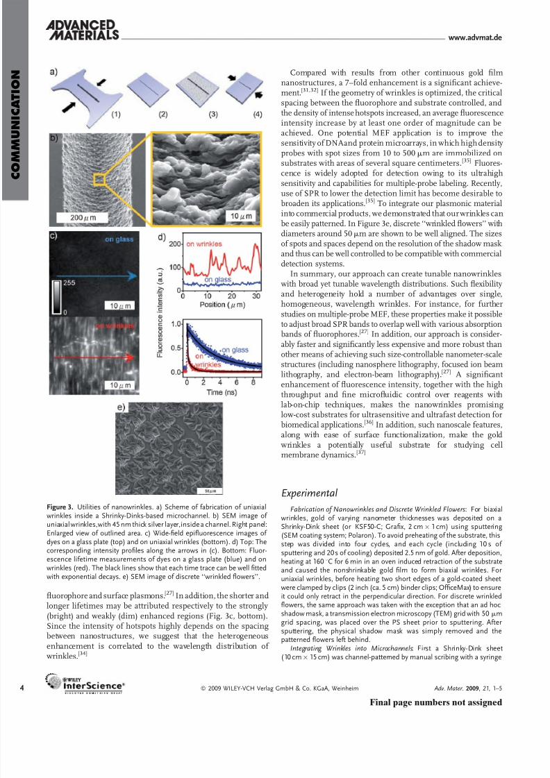
biaxial wrinkles (data not shown), uniaxial wrinkles can bealigned inside the microchannel. As shown in Figure 3a, rst, amicrochannel was patterned on a Shrinky-Dink sheet by manualscribing with a syringe tip. Second, we constrained it to shrink inonly one direction, perpendicular to the direction of the channel.Third, a piece of channel-patterned adhesive tape was placed onits top as a mask during the silver-sputtering. Finally, afterdeposition of 40 nm thick silver, the tape was removed; heatingwithout constraints makes the sheet shrink in the perpendiculardirection and form uniaxial wrinkles. Figure 3b shows that thesewrinkles are perpendicularly aligned within a channel with widthof 280mm. Thermal bonding can be achieved easily as describedin our previous papers. [19,20]
Notably, our ability to achieve nanometer-scale wrinklesenables us to use these self-organized structures for surfaceplasmon resonance (SPR)-based sensing applications, such asmetal-enhanced uorescence (MEF). This technique utilizesmetallic nanostructures in which the plasmons resonate with theuorophores to reduce their excited state lifetimes andsimultaneously increase their uorescence emission intensi-ties.[27] Silver island lms are often used to meet such arequirement, and the typically ca. 10-fold enhancement has beenapplied to improve detection of DNA hybridization [28] andimmunoassay. [29] However, detrimental chemical properties of silver, such as low stability and easy oxidization, inevitably restrict its potential in biomedical applications. Although the enhance-ment factor of gold is smaller, biocompatible gold in discrete
nanostructures is, in contrast, free of these limitations and holdspromise to enhance uorescence intensity of uorophores by afactor of ca. 2–7.[27,30] Recently, utilization of ‘‘continuous’’ goldnanometer-scale features to improve the density of hotspots hasbeen studied; typically, a ca. 0.5- to 5-fold increase of theuorescence intensity can be achieved. [31,32]
Here, we demonstrate that our continuous gold wrinkledsubstrate is useful for MEF as well. Figures 3c and d (top) show uorescence images along with the corresponding intensity proles of dyes, dissolved in polymer solution and thenspin-coated on either a bare glass plate or uniaxial goldwrinkles. [33] The average uorescence intensity increasedapproximately threefold over a relatively large area when thedyes were deposited on the wrinkles rather than the glass. Many
bright lines parallel to the direction of the wrinkles indicates that there are many continuous hotspots along the wrinkles, with 5- to7-fold enhancements. To conrm that the enhancement resultedfrom plasmon effects rather than aggregation of dyes, uores-cence lifetime measurements were performed with a homemadeconfocal microscope with a time-correlated single-photoncounting module. Figure 3d (bottom) shows that the averageuorescence lifetime of dyes on a glass plate is 3.5 ns, but onwrinkles their average lifetime decreases dramatically to 0.4 ns(with a shorter lifetime of 0.3 ns and a longer lifetime of 1.7 ns).This ca. 9-fold decrease in average lifetime suggests that enhancement results from strong interactions between the
Adv. Mater. 2009 , 21, 1–5 ß 2009 WILEY-VCH Verlag GmbH & Co. KGaA, Weinheim 3
Final page numbers not assigned
8/14/2019 2009_shrinky ndinks
http://slidepdf.com/reader/full/2009shrinky-ndinks 4/5
COMMUNICATION
www.advmat.de
uorophore and surface plasmons. [27] In addition, the shorter andlonger lifetimes may be attributed respectively to the strongly (bright) and weakly (dim) enhanced regions (Fig. 3c, bottom).Since the intensity of hotspots highly depends on the spacingbetween nanostructures, we suggest that the heterogeneousenhancement is correlated to the wavelength distribution of wrinkles. [34]
Compared with results from other continuous gold lmnanostructures, a 7–fold enhancement is a signicant achieve-ment. [31,32] If the geometry of wrinkles is optimized, the criticalspacing between the uorophore and substrate controlled, andthe density of intense hotspots increased, an average uorescenceintensity increase by at least one order of magnitude can be
achieved. One potential MEF application is to improve thesensitivity of DNAand protein microarrays, in which highdensity probes with spot sizes from 10 to 500 mm are immobilized onsubstrates with areas of several square centimeters. [35] Fluores-cence is widely adopted for detection owing to its ultrahighsensitivity and capabilities for multiple-probe labeling. Recently,use of SPR to lower the detection limit has become desirable tobroaden its applications. [35] To integrate our plasmonic materialinto commercial products, we demonstrated that ourwrinkles canbe easily patterned. In Figure 3e, discrete ‘‘wrinkled owers’’ withdiameters around 50 mm are shown to be well aligned. The sizesof spots and spaces depend on the resolution of the shadow mask and thus can be well controlled to be compatible with commercialdetection systems.
In summary, our approach can create tunable nanowrinkleswith broad yet tunable wavelength distributions. Such exibility and heterogeneity hold a number of advantages over single,homogeneous, wavelength wrinkles. For instance, for furtherstudies on multiple-probe MEF, these properties make it possibleto adjust broad SPR bands to overlap well with various absorptionbands of uorophores. [27] In addition, our approach is consider-ably faster and signicantly less expensive and more robust thanother means of achieving such size-controllable nanometer-scalestructures (including nanosphere lithography, focused ion beamlithography, and electron-beam lithography). [27] A signicant enhancement of uorescence intensity, together with the highthroughput and ne microuidic control over reagents with
lab-on-chip techniques, makes the nanowrinkles promisinglow-cost substrates for ultrasensitive and ultrafast detection forbiomedical applications. [36] In addition, such nanoscale features,along with ease of surface functionalization, make the goldwrinkles a potentially useful substrate for studying cellmembrane dynamics. [37]
Experimental Fabrication of Nanowrinkles and Discrete Wrinkled Flowers: For biaxial
wrinkles, gold of varying nanometer thicknesses was deposited on aShrinky-Dink sheet (or KSF50-C; Grax, 2 cm 1 cm) using sputtering(SEM coating system; Polaron). To avoid preheating of the substrate, this
step was divided into four cycles, and each cycle (including 10 s of sputtering and 20s of cooling) deposited 2.5 nm of gold. After deposition,heating at 160 8 C for 6 min in an oven induced retraction of the substrateand caused the nonshrinkable gold lm to form biaxial wrinkles. Foruniaxial wrinkles, before heating two short edges of a gold-coated sheetwere clamped by clips (2 inch (ca. 5 cm) binder clips; OfceMax) to ensureit could only retract in the perpendicular direction. For discrete wrinkledowers, the same approach was taken with the exception that an ad hocshadow mask, a transmission electron microscopy (TEM) grid with 50 mmgrid spacing, was placed over the PS sheet prior to sputtering. Aftersputtering, the physical shadow mask was simply removed and thepatterned owers left behind.
Integrating Wrinkles into Microchannels: First a Shrinky-Dink sheet(10 cm  15 cm) was channel-patterned by manual scribing with a syringe
Figure 3. Utilities of nanowrinkles. a) Scheme of fabrication of uniaxialwrinkles inside a Shrinky-Dinks-based microchannel. b) SEM image of uniaxialwrinkles,with 45nm thick silver layer,insidea channel.Right panel:Enlarged view of outlined area. c) Wide-eld epiuorescence images of
dyes on a glass plate (top) and on uniaxial wrinkles (bottom). d) Top: Thecorresponding intensity proles along the arrows in (c). Bottom: Fluor-escence lifetime measurements of dyes on a glass plate (blue) and onwrinkles (red). The black lines show that each time trace can be well ttedwith exponential decays. e) SEM image of discrete ‘‘wrinkled owers’’.
4 ß 2009 WILEY-VCH Verlag GmbH & Co. KGaA, Weinheim Adv. Mater. 2009, 21, 1–5
Final page numbers not assigned

8/14/2019 2009_shrinky ndinks
http://slidepdf.com/reader/full/2009shrinky-ndinks 5/5
www.advmat.de
tip (20 gauge luer stub syringe tip) to remove PS. Next, the sample isconstrained by clips in one direction and allowed to shrink by heating it to150 8 C. After cooling, the center (2.5 cm 5 cm) of the sample was cut outusing a diamond saw. The chip was then masked by placing adhesive tape(3M brand) on the surface of the sample adjacent to the channel previouslyscribed into the surface. The tape was aligned under a dissectionmicroscope until the entire surface was covered and only the channel
remained exposed. The sample was then coated with 45 nm of silver bysputter deposition. Aftercoating, the tapewas removed fromthe surface of the chip; what remained was only the silver that was deposited on thesurface of the channel. The sample was then shrunk, without beingconstrained, at 150 8 C to create uniaxial wrinkles inside the channel.
Materials and Methods for MEF Experiments: Dye molecules (RedCMTPX dyes, CellTracker; Invitrogen) with absorption peaking at 577 nmand emission peaking at 602nm, were used. They were rst dissolved indimethylsulfoxide (Sigma) to a concentration of 10 m M and then dilutedwith poly(vinyl alcohol) solution (PVA, 1 wt% in water, MW ca.13000–23000; Sigma) to ca. 10 mM. Sample (10 mL) was dropped ontothe uniaxial wrinkles (50nm thick gold) and a glass plate and thenspin-coated at 3000 rpm for 2 min to form a sample layer with tens of nanometers thickness [33]. PVA polymers are used to form a buffer layerbetween the metal surface and uorophores to avoid metal-inducedquenching by direct contact [33]. The uorescence images were acquired
using a wide-eld epiuorescence microscope (TE 2000-U; Nikon)equipped with a illumination system (X-Cite Series 120; EXFO) and agreen color excitation lter (D540/25X; Chroma Tech). The emission wascollected by a 40Â , numerical aperture (NA) 0.75 objective (Plan Fluor;Nikon)witha 590–650nm band-passlter (D620/60M; Chroma Tech) andrecorded with a charge-coupled device (CoolSNAP EZ; Photometrics). Foruorescence lifetime measurement, samples were mounted on ahomemade confocal optical microscope for inspection. Excitation of thesamples was performed through a 100 Â , NA 0.7 objective (Nikon) using afrequency-doubled mode-locked ultrafast Ti:Sapphire laser (MIRA 900;Coherent) operating at 410nm with 76 MHz repetition rate. Emissionpassing through a 410nm notch lter (CVI) and a 590–650nm band-passlter (D620/60M; Chroma Tech) wasdetectedby an avalanche photodiode(PDM 50ct; MPD). The corresponding uorescencedecays were measuredwitha time-correlatedsingle-photon countingmodule(PH300; Picoquant).
AcknowledgementsSpecial thanks to Mike Dunlap. This project was supported by NSF COINSand Shrink Nanotechnologies Inc.
Received: July 9, 2009Published online:
[1] K. Emenko, M. Rackaitis, E. Manias, A. Vaziri, L. Mahadevan, J. Genzer,Nat. Mater. 2005 , 4, 293.
[2] E. Cerda, K. Ravi-Chandar, L. Mahadevan,Nature 2002, 419 , 579.[3] Z. Huang, W. Hong, Z. Suo,Phys. Rev. E 2004 , 70 , 030601.[4] J. Y. Chung, A. J. Nolte, C. M. Stafford,Adv. Mater. 2009, 21, 1356.[5] E. Rebollar, I. Frischauf, M. Olbrich, T. Peterbauer, S. Hering, J. Preiner,
P. Hinterdorfer, C. Romanin, J. Heitz, Biomaterials2008, 29 , 1796.
[6] X. F. Wang, C. A. Ohlin, Q. H. Lu, J. Hu,Biomaterials2008, 29 , 2049.[7] H. Q. Jiang, D. Y. Khang, J. Z. Song, Y. G. Sun, Y. G. Huang, J. A. Rogers,
Proc. Natl. Acad. Sci. USA2007, 104, 15607.[8] D. H. Kim, J. H. Ahn, W. M. Choi, H. S. Kim, T. H. Kim, J. Z. Song,
Y. G. Y. Huang, Z. J. Liu, C. Lu, J. A. Rogers,Science2008 , 320 , 507.[9] N. Bowden, S. Brittain, A. G. Evans, J. W. Hutchinson, G. M. Whitesides,
Nature 1998, 393, 146.[10] M. G. Urdaneta, R. Delille, E. Smela,Adv. Mater. 2007, 19 , 2629.[11] S. P. Lacour, S. Wagner, Z. Y. Huang, Z. Suo,Appl. Phys. Lett.2003, 82,
2404.[12] C. M. Stafford, C. Harrison, K. L. Beers, A. Karim, E. J. Amis,
M. R. Vanlandingham, H. C. Kim, W. Volksen, R. D. Miller,E. E. Simonyi,Nat. Mater. 2004, 3, 545.
[13] H. D. Rowland, W. P. King, J. B. Pethica, G. L. Cross,Science2008, 322,720.
[14] F. Yang, E. Wornyo, K. Gall, W. P. King,Nanotechnology2007 , 18, 285302.[15] W. T. S. Huck, N. Bowden, P. Onck, T. Pardoen, J. W. Hutchinson,
G. M. Whitesides, Langmuir 2000 , 16 , 3497.[16] M. Watanabe, T. Hirai,J. Polym. Sci, Part B: Polym. Phys.2004, 42, 2460.[17] P. J. Yoo, K. Y. Suh, S. Y. Park, H. H. Lee,Adv. Mater. 2002 , 14, 1383.[18] M. Long, M. A. Sprague, A. Grimes, B. D. Rich, M. Khine,Appl. Phys. Lett.
2009 , 94, 133501.[19] A. Grimes, D. N. Breslauer, M. Long, J. Pegan, L. P. Lee, M. Khine,Lab Chip
2008 , 8, 170.[20] C. S. Chen, D. N. Breslauer, J. I. Luna, A. Grimes, W. C. Chin, L. P. Lee,
M. Khine, Lab Chip2008, 8, 622.[21] J. Genzer, J. Groenewold,Soft Matter 2006, 2, 310.[22] J. Groenewold,Physica A2001, 298, 32.[23] B. Wu, A. Heidelberg, J. J. Boland,Nat. Mater. 2005 , 4, 525.[24] J. H. Zhao, M. Kiene, C. Hu, P. S. Ho,Appl. Phys. Lett.2000 , 77 ,
2843.[25] M. D. Uchic, D. M. Dimiduk, J. N. Florando, W. D. Nix,Science2004, 305,
986.[26] F. Avile´ s, L. Llanes, A. I. Oliva,J. Mater. Sci.2009, 44, 2590.[27] J. R. Lakowicz, K. Ray, M. Chowdhury, H. Szmacinski, Y. Fu, J. Zhang,
K. Nowaczyk,Analyst2008 , 133, 1308.[28] J. Malicka, I. Gryczynski, J. R. Lakowicz,Biochem. Biophys. Res. Commun.
2003 , 306 , 213.[29] E. G. Matveeva, Z. Gryczynski, J. R. Lakowicz,J. Immunol. Methods2005,
302, 26.[30] J. Zhang, J. R. Lakowicz,Opt. Express2007 , 15, 2598.[31] I. Abdulhalim, A. Karabchevsky, C. Patzig, B. Rauschenbach, B. Fuhrmann,
E. Eltzov, R. Marks, J. Xu, F. Zhang, A. Lakhtakia,Appl. Phys. Lett.2009 , 94,063106.
[32] K. Matsuda, Y. Ito, Y. Kanemitsu,Appl. Phys. Lett.2008, 92, 211911.[33] K. Ray, R. Badugu, J. R. Lakowicz,J. Am. Chem. Soc.2006, 128,
8998.[34] J. Zhang, Y. Fu, M. H. Chowdhury, J. R. Lakowicz,Nano Lett. 2007 , 7 ,
2101.[35] M. Bally, M. Halter, J. Voros, H. M. Grandin,Surf. Interface Anal.2006 , 38,
1442.[36] S. Chung,J. H. Lee, M. W. Moon, J. Han, R. D. Kamm, Adv. Mater.2008, 20 ,
3011.[37] K. Kim, D. J. Kim, E. J. Cho, J. S. Suh, Y. M. Huh, D. Kim,Nanotechnology
2009 , 20 .
Adv. Mater. 2009 , 21, 1–5 ß 2009 WILEY-VCH Verlag GmbH & Co. KGaA, Weinheim 5
Final page numbers not assigned


