Embed Size (px)
Citation preview

1Integrated Silicon Solution, Inc. Rev. N05/25/2015
Copyright © 2014 Integrated Silicon Solution, Inc. All rights reserved. ISSI reserves the right to make changes to this specification and its products at any time without notice. ISSI assumes no liability arising out of the application or use of any information, products or services described herein. Customers are advised to obtain the latest version of this device specification before relying on any published information and before placing orders for products.
IS61LPS51218A, IS61LPS25636A, IS61LPS25632A, IS64LPS25636A,IS61VPS51218A, IS61VPS25636A
FEATURES
• Internalself-timedwritecycle
• IndividualByteWriteControlandGlobalWrite
• Clockcontrolled,registeredaddress,dataandcontrol
• BurstsequencecontrolusingMODEinput
• Threechipenableoptionforsimpledepthex-pansion and address pipelining
• Commondatainputsanddataoutputs
• AutoPower-downduringdeselect
• Singlecycledeselect
• SnoozeMODEforreduced-powerstandby
• JTAGBoundaryScanforBGApackage
• PowerSupply
LPS:Vdd 3.3V + 5%, Vddq 3.3V/2.5V + 5%
VPS:Vdd 2.5V + 5%, Vddq 2.5V + 5%
• JEDEC100-PinQFP,119-ballBGA,and165-ballBGApackages
• Lead-freeavailable
DESCRIPTION
The ISSI IS61LPS/VPS25636A, IS61LPS25632A,IS64LPS25636A and IS61LPS/VPS51218A are high-speed, low-power synchronous static RAMs designed to provide burstable, high-performance memory for com-municationandnetworkingapplications.TheIS61LPS/VPS25636A and IS64LPS25636A are organized as262,144 words by 36 bits. The IS61LPS25632A is organizedas262,144wordsby32bits.TheIS61LPS/VPS51218Aisorganizedas524,288wordsby18bits.Fabricated with ISSI's advanced CMOS technology,thedeviceintegratesa2-bitburstcounter,high-speedSRAMcore,andhigh-drivecapabilityoutputsintoasinglemonolithic circuit. All synchronous inputs pass through registerscontrolledbyapositive-edge-triggeredsingleclock input.
Writecyclesareinternallyself-timedandareinitiatedbytherisingedgeoftheclockinput.Writecyclescanbeone to four bytes wide as controlled by the write control inputs.
Separate byte enables allow individual bytes to be written. Thebytewriteoperationisperformedbyusingthebytewrite enable (BWE) input combined with one or more individual byte write signals (BWx). Inaddition,GlobalWrite(GW) is available for writing all bytes at one time, regardless of the byte write controls.
BurstscanbeinitiatedwitheitherADSP (Address Status Processor)orADSC (Address Status Cache Controller) inputpins.Subsequentburstaddressescanbegener-ated internally and controlled by the ADV (burst address advance) input pin.
Themodepinisusedtoselecttheburstsequenceor-der,LinearburstisachievedwhenthispinistiedLOW.InterleaveburstisachievedwhenthispinistiedHIGHor left floating.
256K x 36, 256K x 32, 512K x 18 9 Mb SYNCHRONOUS PIPELINED, SINgLE CYCLE DESELECT STATIC RAM
JUNE 2015
FAST ACCESS TIME Symbol Parameter 250 200 166 Units
tkq ClockAccessTime 2.6 3.1 3.5 ns
tkc CycleTime 4 5 6 ns
Frequency 250 200 166 MHz

2 Integrated Silicon Solution, Inc. Rev. N
05/25/2015
IS61LPS51218A, IS61LPS25636A, IS61LPS25632A, IS64LPS25636A,IS61VPS51218A, IS61VPS25636A
BLOCK DIAGRAM
18/19
BINARYCOUNTER
GW
CLR
CE
CLK Q0
Q1
MODE
A0'A0
A1A1'
CLK
ADV
ADSCADSP
16/17 18/19
ADDRESSREGISTERCE
D
CLK
Q
DQ(a-d)BYTE WRITEREGISTERS
D
CLK
Q
ENABLEREGISTERCE
D
CLK
Q
ENABLEDELAY
REGISTER
D
CLK
Q
BWEBW(a-d)x18: a,b
x32/x36: a-d
CE
CE2
CE2
256Kx32;256Kx36;512Kx18
MEMORY ARRAY
32, 36,or 18
INPUTREGISTERS
CLK
OUTPUTREGISTERS
CLK
OE
2/4/8
OEDQa - DQd
32, 36,or 18
32, 36,or 18
A
POWERDOWN
ZZ
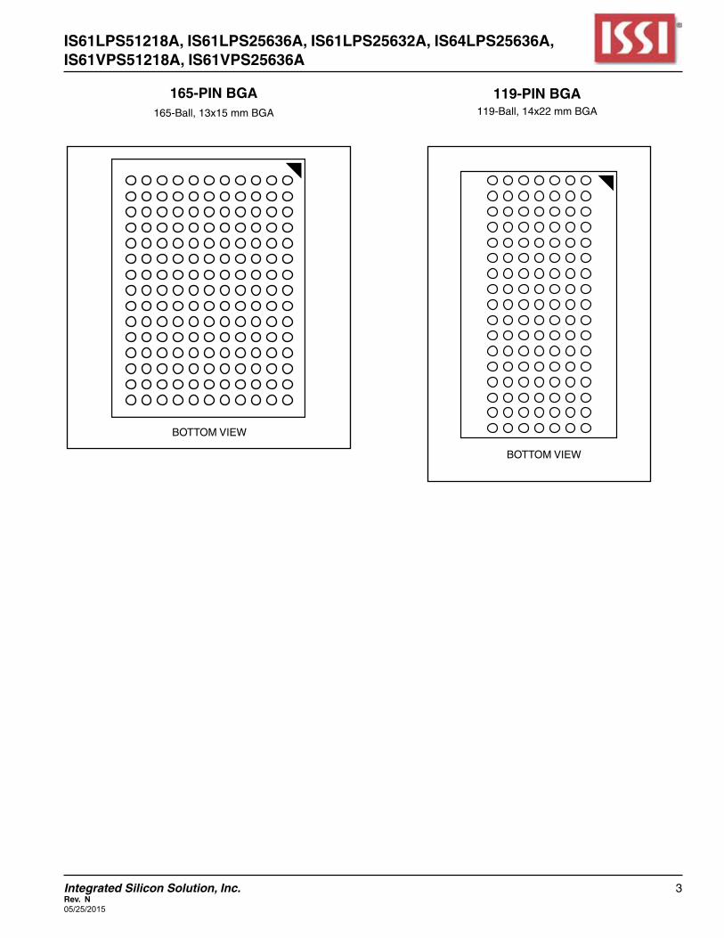
Integrated Silicon Solution, Inc. 3Rev. N05/25/2015
IS61LPS51218A, IS61LPS25636A, IS61LPS25632A, IS64LPS25636A,IS61VPS51218A, IS61VPS25636A
BOTTOMVIEW
BOTTOMVIEW
165-PIN BgA165-Ball,13x15mmBGA
119-PIN BgA119-Ball,14x22mmBGA
4 Integrated Silicon Solution, Inc. Rev. N
05/25/2015
IS61LPS51218A, IS61LPS25636A, IS61LPS25632A, IS64LPS25636A,IS61VPS51218A, IS61VPS25636A
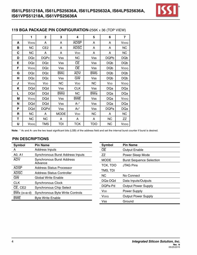
119 BGA PACKAGE PIN CONFIGURATION-256k x 36 (TOP VIEW)
PIN DESCRIPTIONS
1 2 3 4 5 6 7
A VDDQ A A ADSP A A VDDQ
B NC CE2 A ADSC A A NC
C NC A A VDD A A NC
D DQc DQPc Vss NC Vss DQPb DQb
E DQc DQc Vss CE Vss DQb DQb
F VDDQ DQc Vss OE Vss DQb VDDQ
g DQc DQc BWc ADV BWb DQb DQb
H DQc DQc Vss GW Vss DQb DQb
J VDDQ VDD NC VDD NC VDD VDDQ
K DQd DQd Vss CLK Vss DQa DQa
L DQd DQd BWd NC BWa DQa DQa
M VDDQ DQd Vss BWE Vss DQa VDDQ
N DQd DQd Vss A1* Vss DQa DQa
P DQd DQPd Vss A0* Vss DQPa DQa
R NC A MODE VDD NC A NC
T NC NC A A A NC ZZ
U VDDQ TMS TDI TCK TDO NC VDDQ
Symbol Pin NameA Address Inputs
A0, A1 SynchronousBurstAddressInputs
ADV SynchronousBurstAddressAdvance
ADSP AddressStatusProcessor
ADSC Address Status Controller
GW GlobalWriteEnable
CLK Synchronous Clock
CE,CE2 Synchronous Chip Select
BWx(x=a-d) SynchronousByteWriteControls
BWE ByteWriteEnable
Symbol Pin Name
OE OutputEnable
ZZ PowerSleepMode
MODE BurstSequenceSelection
TCK,TDO JTAGPins
TMS,TDI
NC No Connect
DQa-DQd DataInputs/Outputs
DQPa-Pd OutputPowerSupply
Vdd PowerSupply
Vddq OutputPowerSupply
Vss Ground
Note: * A0 and A1arethetwoleastsignificantbits(LSB)oftheaddressfieldandsettheinternalburstcounterifburstisdesired.

5Integrated Silicon Solution, Inc. Rev. N05/25/2015
IS61LPS51218A, IS61LPS25636A, IS61LPS25632A, IS64LPS25636A,IS61VPS51218A, IS61VPS25636A
119 BGA PACKAGE PIN CONFIGURATION512kx18 (TOP VIEW)
PIN DESCRIPTIONS
Note: * A0 and A1arethetwoleastsignificantbits(LSB)oftheaddressfieldandsettheinternalburstcounterifburstisdesired.
1 2 3 4 5 6 7
A VDDQ A A ADSP A A VDDQ
B NC CE2 A ADSC A A NC
C NC A A VDD A A NC
D DQb NC Vss NC Vss DQPa NC
E NC DQb Vss CE Vss NC DQa
F VDDQ NC Vss OE Vss DQa VDDQ
g NC DQb BWb ADV Vss NC DQa
H DQb NC Vss GW Vss DQa NC
J VDDQ VDD NC VDD NC VDD VDDQ
K NC DQb Vss CLK Vss NC DQa
L DQb NC Vss NC BWa DQa NC
M VDDQ DQb Vss BWE Vss NC VDDQ
N DQb NC Vss A1* Vss DQa NC
P NC DQPb Vss A0* Vss NC DQa
R NC A MODE VDD NC A NC
T NC A A NC A A ZZ
U VDDQ TMS TDI TCK TDO NC VDDQ
Symbol Pin NameA Address Inputs
A0, A1 SynchronousBurstAddressInputs
ADV SynchronousBurstAddressAdvance
ADSP AddressStatusProcessor
ADSC Address Status Controller
GW GlobalWriteEnable
CLK Synchronous Clock
CE,CE2 Synchronous Chip Select
BWx(x=a,b) SynchronousByteWriteControls
BWE ByteWriteEnable
Symbol Pin Name
OE OutputEnable
ZZ PowerSleepMode
MODE BurstSequenceSelection
TCK,TDO JTAGPins
TMS,TDI
NC No Connect
DQa-DQb DataInputs/Outputs
DQPa-Pb OutputPowerSupply
Vdd PowerSupply
Vddq OutputPowerSupply
Vss Ground

6 Integrated Silicon Solution, Inc. Rev. N
05/25/2015
IS61LPS51218A, IS61LPS25636A, IS61LPS25632A, IS64LPS25636A,IS61VPS51218A, IS61VPS25636A
PIN DESCRIPTIONS
165 BGA PACKAGE PIN CONFIGURATION256k x 36 (TOP VIEW)
Note: * A0 and A1arethetwoleastsignificantbits(LSB)oftheaddressfieldandsettheinternalburstcounterifburstisdesired.
1 2 3 4 5 6 7 8 9 10 11
A NC A CE BWc BWb CE2 BWE ADSC ADV A NC
B NC A CE2 BWd BWa CLK GW OE ADSP A NC
C DQPc NC Vddq Vss Vss Vss Vss Vss Vddq Nc DQPb
D DQc DQc Vddq Vdd Vss Vss Vss Vdd Vddq DQb DQb
E DQc DQc Vddq Vdd Vss Vss Vss Vdd Vddq DQb DQb
F DQc DQc Vddq Vdd Vss Vss Vss Vdd Vddq DQb DQb
g DQc DQc Vddq Vdd Vss Vss Vss Vdd Vddq DQb DQb
H NC Vss NC Vdd Vss Vss Vss Vdd Nc Nc ZZ
J DQd DQd Vddq Vdd Vss Vss Vss Vdd Vddq dqa dqa
K DQd DQd Vddq Vdd Vss Vss Vss Vdd Vddq dqa dqa
L DQd DQd Vddq Vdd Vss Vss Vss Vdd Vddq dqa dqa
M DQd DQd Vddq Vdd Vss Vss Vss Vdd Vddq dqa dqa
N DQPd NC Vddq Vss NC NC NC Vss Vddq NC DQPa
P NC NC A A TDI A1* TDO A A A A
R MODE NC A A TMS A0* TCK A A A A
Symbol Pin NameA Address Inputs
A0, A1 SynchronousBurstAddressInputs
ADV SynchronousBurstAddressAdvance
ADSP AddressStatusProcessor
ADSC Address Status Controller
GW GlobalWriteEnable
CLK Synchronous Clock
CE, CE2, CE2 Synchronous Chip Select
BWx(x=a,b,c,d) SynchronousByteWriteControls
Symbol Pin Name
BWE ByteWriteEnable
OE OutputEnable
ZZ PowerSleepMode
MODE BurstSequenceSelection
TCK,TDO JTAGPinsTMS,TDI
NC No Connect
DQx DataInputs/Outputs
DQPx DataInputs/Outputs
Vdd 3.3V/2.5VPowerSupply
Vddq IsolatedOutputPowerSupply3.3V/2.5V
Vss Ground

7Integrated Silicon Solution, Inc. Rev. N05/25/2015
IS61LPS51218A, IS61LPS25636A, IS61LPS25632A, IS64LPS25636A,IS61VPS51218A, IS61VPS25636A
Note: * A0 and A1arethetwoleastsignificantbits(LSB)oftheaddressfieldandsettheinternalburstcounterifburstisdesired.
165 BGA PACKAGE PIN CONFIGURATION512k x 18 (TOP VIEW)
PIN DESCRIPTIONS
1 2 3 4 5 6 7 8 9 10 11
A NC A CE BWb NC CE2 BWE ADSC ADV A A
B NC A CE2 NC BWa CLK GW OE ADSP A NC
C NC NC Vddq Vss Vss Vss Vss Vss Vddq Nc DQPa
D NC DQb Vddq Vdd Vss Vss Vss Vdd Vddq NC DQa
E NC DQb Vddq Vdd Vss Vss Vss Vdd Vddq NC DQa
F NC DQb Vddq Vdd Vss Vss Vss Vdd Vddq NC DQa
g NC DQb Vddq Vdd Vss Vss Vss Vdd Vddq NC DQa
H NC Vss NC Vdd Vss Vss Vss Vdd Nc Nc ZZ
J DQb NC Vddq Vdd Vss Vss Vss Vdd Vddq dqa Nc
K DQb NC Vddq Vdd Vss Vss Vss Vdd Vddq dqa Nc
L DQb NC Vddq Vdd Vss Vss Vss Vdd Vddq dqa Nc
M DQb NC Vddq Vdd Vss Vss Vss Vdd Vddq dqa Nc
N DQPb NC Vddq Vss NC NC NC Vss Vddq NC NC
P NC NC A A TDI A1* TDO A A A A
R MODE NC A A TMS A0* TCK A A A A
Symbol Pin NameA Address Inputs
A0, A1 SynchronousBurstAddressInputs
ADV SynchronousBurstAddressAdvance
ADSP AddressStatusProcessor
ADSC Address Status Controller
GW GlobalWriteEnable
CLK Synchronous Clock
CE, CE2, CE2 Synchronous Chip Select
BWx(x=a,b) SynchronousByteWriteControls
Symbol Pin Name
BWE ByteWriteEnable
OE OutputEnable
ZZ PowerSleepMode
MODE BurstSequenceSelection
TCK,TDO JTAGPinsTMS,TDI
NC No Connect
DQx DataInputs/Outputs
DQPx DataInputs/Outputs
Vdd 3.3V/2.5VPowerSupply
Vddq IsolatedOutputPowerSupply3.3V/2.5V
Vss Ground
8 Integrated Silicon Solution, Inc. Rev. N
05/25/2015
IS61LPS51218A, IS61LPS25636A, IS61LPS25632A, IS64LPS25636A,IS61VPS51218A, IS61VPS25636A
DQPbDQbDQbVDDQVSSDQbDQbDQbDQbVSSVDDQDQbDQbVSSNCVDDZZDQaDQaVDDQVSSDQaDQaDQaDQaVSSVDDQDQaDQaDQPa
A A CE
CE
2BWd
BWc
BWb
BWa
CE2
VD
DV
SS
CLKGWBWE
OEADSC
ADSP
ADV
A A
DQPcDQcDQc
VDDQVSSDQcDQcDQcDQcVSS
VDDQDQcDQcNC
VDDNC
VSSDQdDQd
VDDQVSSDQdDQdDQdDQdVSS
VDDQDQdDQd
DQPd
123456789101112131415161718192021222324252627282930
807978777675747372717069686766656463626160595857565554535251
100 99 98 97 96 95 94 93 92 91 90 89 88 87 86 85 84 83 82 81
31 32 33 34 35 36 37 38 39 40 41 42 43 44 45
MO
DE A A A A A1
A0
NC
NC
VS
SV
DD
NC A A A A A A A A
46 47 48 49 50
PIN DESCRIPTIONS
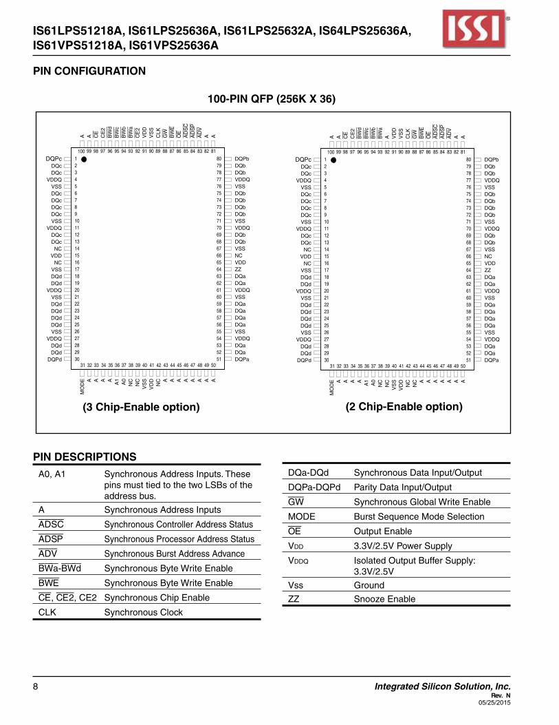
A0, A1 SynchronousAddressInputs.ThesepinsmusttiedtothetwoLSBsoftheaddress bus.
A Synchronous Address Inputs
ADSC Synchronous Controller Address Status
ADSP SynchronousProcessorAddressStatus
ADV SynchronousBurstAddressAdvance
BWa-BWd SynchronousByteWriteEnable
BWE SynchronousByteWriteEnable
CE, CE2, CE2 SynchronousChipEnable
CLK Synchronous Clock
DQa-DQd SynchronousDataInput/Output
DQPa-DQPd ParityDataInput/Output
GW SynchronousGlobalWriteEnable
MODE BurstSequenceModeSelection
OE OutputEnable
Vdd 3.3V/2.5VPowerSupply
Vddq IsolatedOutputBufferSupply: 3.3V/2.5V
Vss Ground
ZZ SnoozeEnable
PIN CONFIGURATION
(3 Chip-Enable option)
100-PIN QFP (256K x 36)
DQPbDQbDQbVDDQVSSDQbDQbDQbDQbVSSVDDQDQbDQbVSSNCVDDZZDQaDQaVDDQVSSDQaDQaDQaDQaVSSVDDQDQaDQaDQPa
A A CE
CE
2BWd
BWc
BWb
BWa
A VD
DV
SS
CLKGWBWE
OEADSC
ADSP
ADV
A A
DQPcDQcDQc
VDDQVSSDQcDQcDQcDQcVSS
VDDQDQcDQc
NCVDD
NCVSSDQdDQd
VDDQVSSDQdDQdDQdDQdVSS
VDDQDQdDQd
DQPd
123456789101112131415161718192021222324252627282930
807978777675747372717069686766656463626160595857565554535251
100 99 98 97 96 95 94 93 92 91 90 89 88 87 86 85 84 83 82 81
31 32 33 34 35 36 37 38 39 40 41 42 43 44 45
MO
DE A A A A A1
A0
NC
NC
VS
SV
DD
NC
NC A A A A A A A
46 47 48 49 50
(2 Chip-Enable option)
9Integrated Silicon Solution, Inc. Rev. N05/25/2015
IS61LPS51218A, IS61LPS25636A, IS61LPS25632A, IS64LPS25636A,IS61VPS51218A, IS61VPS25636A
NCDQbDQbVDDQVSSDQbDQbDQbDQbVSSVDDQDQbDQbVSSNCVDDZZDQaDQaVDDQVSSDQaDQaDQaDQaVSSVDDQDQaDQaNC
A A CE
CE
2BWd
BWc
BWb
BWa
CE2
VD
DV
SS
CLKGWBWE
OEADSC
ADSP
ADV
A A
NCDQcDQc
VDDQVSSDQcDQcDQcDQcVSS
VDDQDQcDQcNC
VDDNC
VSSDQdDQd
VDDQVSSDQdDQdDQdDQdVSS
VDDQDQdDQd
NC
123456789101112131415161718192021222324252627282930
807978777675747372717069686766656463626160595857565554535251
100 99 98 97 96 95 94 93 92 91 90 89 88 87 86 85 84 83 82 81
31 32 33 34 35 36 37 38 39 40 41 42 43 44 45
MO
DE A A A A A1
A0
NC
NC
VS
SV
DD
NC A A A A A A A A
46 47 48 49 50
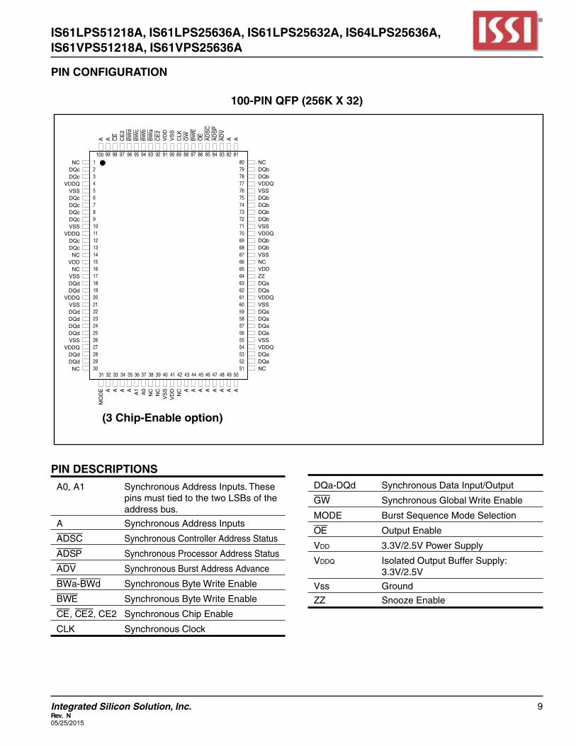
PIN DESCRIPTIONS
A0, A1 SynchronousAddressInputs.ThesepinsmusttiedtothetwoLSBsoftheaddress bus.
A Synchronous Address Inputs
ADSC Synchronous Controller Address Status
ADSP SynchronousProcessorAddressStatus
ADV SynchronousBurstAddressAdvance
BWa-BWd SynchronousByteWriteEnable
BWE SynchronousByteWriteEnable
CE, CE2, CE2 SynchronousChipEnable
CLK Synchronous Clock
DQa-DQd SynchronousDataInput/Output
GW SynchronousGlobalWriteEnable
MODE BurstSequenceModeSelection
OE OutputEnable
Vdd 3.3V/2.5VPowerSupply
Vddq IsolatedOutputBufferSupply: 3.3V/2.5V
Vss Ground
ZZ SnoozeEnable
PIN CONFIGURATION
(3 Chip-Enable option)
100-PIN QFP (256K x 32)

10 Integrated Silicon Solution, Inc. Rev. N
05/25/2015
IS61LPS51218A, IS61LPS25636A, IS61LPS25632A, IS64LPS25636A,IS61VPS51218A, IS61VPS25636A
PIN CONFIGURATION
(3 Chip-Enable Option)
PIN DESCRIPTIONS
A0,A1 SynchronousAddressInputs.ThesepinsmusttiedtothetwoLSBsoftheaddress bus.
A Synchronous Address Inputs
ADSC Synchronous Controller Address Status
ADSP SynchronousProcessorAddressStatus
ADV SynchronousBurstAddressAdvance
BWa-BWb SynchronousByteWriteEnable
BWE SynchronousByteWriteEnable
CE,CE2,CE2 SynchronousChipEnable
CLK Synchronous Clock
DQa-DQb SynchronousDataInput/Output
DQPa-DQPb ParityDataI/O;DQPaisparityforDQa1-8;DQPbisparityforDQb1-8
GW SynchronousGlobalWriteEnable
MODE BurstSequenceModeSelection
OE OutputEnable
Vdd 3.3V/2.5VPowerSupply
Vddq IsolatedOutputBufferSupply: 3.3V/2.5V
Vss Ground
ZZ SnoozeEnable
100-PIN QFP (512K x 18)
ANCNCVDDQVSSNCDQPaDQaDQaVSSVDDQDQaDQaVSSNCVDDZZDQaDQaVDDQVSSDQaDQaNCNCVSSVDDQNCNCNC
A A CE
CE
2N
CN
CBWb
BWa
CE2
VD
DV
SS
CLKGWBWE
OEADSC
ADSP
ADV
A A
NCNCNC
VDDQVSS
NCNC
DQbDQbVSS
VDDQDQbDQb
NCVDD
NCVSSDQbDQb
VDDQVSSDQbDQb
DQPbNC
VSSVDDQ
NCNCNC
123456789101112131415161718192021222324252627282930
807978777675747372717069686766656463626160595857565554535251
100 99 98 97 96 95 94 93 92 91 90 89 88 87 86 85 84 83 82 81
31 32 33 34 35 36 37 38 39 40 41 42 43 44 45
MO
DE A A A A A1
A0
NC
NC
VS
SV
DD
NC A A A A A A A A
46 47 48 49 50
(2 Chip-Enable Option)
ANCNCVDDQ
VSSNCDQPaDQaDQaVSSVDDQ
DQaDQaVSSNCVDD
ZZDQaDQaVDDQ
VSSDQaDQaNCNCVSSVDDQ
NCNCNC
A A CE
CE
2N
CN
CBWb
BWa
A VD
D
VS
SC
LKGWBWE
OEADSC
ADSP
ADV
A A
NCNCNC
VDDQ
VSSNCNC
DQbDQbVSS
VDDQ
DQbDQb
NCVDD
NCVSSDQbDQbVDDQ
VSSDQbDQb
DQPbNC
VSSVDDQ
NCNCNC
123456789101112131415161718192021222324252627282930
807978777675747372717069686766656463626160595857565554535251
100 99 98 97 96 95 94 93 92 91 90 89 88 87 86 85 84 83 82 81
31 32 33 34 35 36 37 38 39 40 41 42 43 44 45
MO
DE A A A A A1
A0
NC
NC
VS
SV
DD
NC
NC A A A A A A A
46 47 48 49 50

11Integrated Silicon Solution, Inc. Rev. N05/25/2015
IS61LPS51218A, IS61LPS25636A, IS61LPS25632A, IS64LPS25636A,IS61VPS51218A, IS61VPS25636A
PARTIAL TRUTH TABLEFunction GW BWE BWa BWb BWc BWd
Read H H X X X X
Read H L H H H H
WriteByte1 H L L H H H
WriteAllBytes H L L L L L
WriteAllBytes L X X X X X
TRUTH TABLE(1-8)
OPERATION ADDRESS CE CE2 CE2 ZZ ADSP ADSC ADV WRITE OE CLK DQDeselectCycle,Power-Down None H X X L X L X X X L-H High-ZDeselectCycle,Power-Down None L X L L L X X X X L-H High-ZDeselectCycle,Power-Down None L H X L L X X X X L-H High-ZDeselectCycle,Power-Down None L X L L H L X X X L-H High-ZDeselectCycle,Power-Down None L H X L H L X X X L-H High-ZSnoozeMode,Power-Down None X X X H X X X X X X High-ZReadCycle,BeginBurst External L L H L L X X X L L-H QReadCycle,BeginBurst External L L H L L X X X H L-H High-ZWriteCycle,BeginBurst External L L H L H L X L X L-H DReadCycle,BeginBurst External L L H L H L X H L L-H QReadCycle,BeginBurst External L L H L H L X H H L-H High-ZReadCycle,ContinueBurst Next X X X L H H L H L L-H QReadCycle,ContinueBurst Next X X X L H H L H H L-H High-ZReadCycle,ContinueBurst Next H X X L X H L H L L-H QReadCycle,ContinueBurst Next H X X L X H L H H L-H High-ZWriteCycle,ContinueBurst Next X X X L H H L L X L-H DWriteCycle,ContinueBurst Next H X X L X H L L X L-H DReadCycle,SuspendBurst Current X X X L H H H H L L-H QReadCycle,SuspendBurst Current X X X L H H H H H L-H High-ZReadCycle,SuspendBurst Current H X X L X H H H L L-H QReadCycle,SuspendBurst Current H X X L X H H H H L-H High-ZWriteCycle,SuspendBurst Current X X X L H H H L X L-H DWriteCycle,SuspendBurst Current H X X L X H H L X L-H D
NOTE: 1. Xmeans“Don’tCare.”HmeanslogicHIGH.LmeanslogicLOW.2. ForWRITE, L means one or more byte write enable signals (BWa-d) and BWEareLOWorGWisLOW.WRITE=Hforall
BWx, BWE, GWHIGH.3. BWaenablesWRITEstoDQa’sandDQPa.BWbenablesWRITEstoDQb’sandDQPb.BWcenablesWRITEstoDQc’s andDQPc.BWdenablesWRITEstoDQd’sandDQPd.DQPaandDQPbareavailableonthex18version. DQPa-DQPdareavail-ableonthex36version.
4. AllinputsexceptOEandZZmustmeetsetupandholdtimesaroundtherisingedge(LOWtoHIGH)ofCLK.5. Waitstatesareinsertedbysuspendingburst.6. ForaWRITEoperationfollowingaREADoperation,OEmustbeHIGHbeforetheinputdatasetuptimeandheldHIGHduring
the input data hold time.7. ThisdevicecontainscircuitrythatwillensuretheoutputswillbeinHigh-Zduringpower-up.8. ADSPLOWalwaysinitiatesaninternalREADattheL-HedgeofCLK.AWRITEisperformedbysettingoneormorebytewrite
enable signals and BWELOWorGWLOWforthesubsequentL-HedgeofCLK.SeeWRITEtimingdiagramforclarification.

12 Integrated Silicon Solution, Inc. Rev. N
05/25/2015
IS61LPS51218A, IS61LPS25636A, IS61LPS25632A, IS64LPS25636A,IS61VPS51218A, IS61VPS25636A
INTERLEAVED BURST ADDRESS TABLE (MODE = VDD or No Connect)External Address 1st Burst Address 2nd Burst Address 3rd Burst Address
A1 A0 A1 A0 A1 A0 A1 A0
00 01 10 11 01 00 11 10 10 11 00 01 11 10 01 00
LINEAR BURST ADDRESS TABLE (MODE = VSS)
0,0
1,0
0,1A1', A0' = 1,1
ABSOLUTE MAxIMUM RATINgS(1)
Symbol Parameter Value UnitTsTg StorageTemperature –55to+150 °CPd PowerDissipation 1.6 WIOuT OutputCurrent(perI/O) 100 mAVIN, VOuT VoltageRelativetoVssforI/OPins –0.5toVddq + 0.5 VVIN VoltageRelativetoVssfor –0.5toVdd + 0.5 V
for Address and Control InputsVdd VoltageonVddSupplyRelativetoVss –0.5to4.6 V
Notes:1. StressgreaterthanthoselistedunderABSOLUTEMAXIMUMRATINGSmaycauseperma-nentdamagetothedevice.Thisisastressratingonlyandfunctionaloperationofthedeviceat these or any other conditions above those indicated in the operational sections of this specificationisnotimplied.Exposuretoabsolutemaximumratingconditionsforextendedperiods may affect reliability.
2.Thisdevicecontainscircuitytoprotecttheinputsagainstdamageduetohighstaticvoltagesorelectricfields;however,precautionsmaybe taken toavoidapplicationofanyvoltagehigherthanmaximumratedvoltagestothishigh-impedancecircuit.
3.ThisdevicecontainscircuitrythatwillensuretheoutputdevicesareinHigh-Zatpowerup.

13Integrated Silicon Solution, Inc.Rev. N05/25/2015
IS61LPS51218A, IS61LPS25636A, IS61LPS25632A, IS64LPS25636A,IS61VPS51218A, IS61VPS25636A
OPERATINg RANgE (IS61LPSxxxxx)Range Ambient Temperature VDD VDDq
Commercial 0°Cto+70°C 3.3V+5% 3.3V/2.5V+5%
Industrial –40°Cto+85°C 3.3V+5% 3.3V/2.5V+5%
OPERATINg RANgE (IS61VPSxxxxx)Range Ambient Temperature VDD VDDq
Commercial 0°Cto+70°C 2.5V+5% 2.5V+5%
Industrial –40°Cto+85°C 2.5V+5% 2.5V+5%
DC ELECTRICAL CHARACTERISTICS (OverOperatingRange)3.3V 2.5V
Symbol Parameter Test Conditions Min. Max. Min. Max. Unit
VOh OutputHIGHVoltage IOh = –4.0mA(3.3V) 2.4 — 2.0 — VIOh = –1.0mA(2.5V)
VOl OutputLOWVoltage IOl = 8.0mA(3.3V) — 0.4 — 0.4 VIOl = 1.0mA(2.5V)
VIh InputHIGHVoltage 2.0 Vdd +0.3 1.7 Vdd + 0.3 V
VIl InputLOWVoltage -0.3 0.8 -0.3 0.7 V
IlI InputLeakageCurrent Vss≤ VIN ≤ Vdd(1) -5 5 -5 5 µA
IlO OutputLeakageCurrent Vss≤ VOuT ≤ Vddq, -5 5 -5 5 µA OE = VIh
OPERATINg RANgE (IS64LPSxxxxx)Range Ambient Temperature VDD VDDq
Automotive –40°Cto+125°C 3.3V+5% 3.3V/2.5V+5%

14 Integrated Silicon Solution, Inc. Rev. N
05/25/2015
IS61LPS51218A, IS61LPS25636A, IS61LPS25632A, IS64LPS25636A,IS61VPS51218A, IS61VPS25636A
POWER SUPPLY CHARACTERISTICS(1) (OverOperatingRange)
-250 -200 -166 MAx MAx MAx
Symbol Parameter Test Conditions Temp. range x18 x36 x18 x36 x18 x36 Unit
Icc ACOperating DeviceSelected, Com. 275 275 250 250 225 225 mA Supply Current OE = VIh, ZZ ≤ VIl, Ind. 300 300 275 275 250 250
All Inputs ≤ 0.2V or Auto. 300 300 ≥ Vdd – 0.2V, CycleTime≥ tkc min.
Isb StandbyCurrent DeviceDeselected, Com. 150 150 150 150 150 150 mA TTLInput Vdd = Max., Ind. 150 150 150 150 150 150
All Inputs ≤ VIl or ≥ VIh, AuTO. 200 200 ZZ ≤ VIl, f=Max.
IsbI StandbyCurrent DeviceDeselected, Com. 100 100 100 100 100 100 mA cMOs Input Vdd = Max., Ind. 105 105 105 105 105 105
VIN ≤Vss +0.2Vor Auto. 130 130
≥Vdd –0.2Vf=0
Note:1. MODEpinhasaninternalpullupandshouldbetiedtoVddorVss.Itexhibits±100µAmaximumleakagecurrentwhentiedto≤Vss+0.2Vor≥Vdd–0.2V.
15Integrated Silicon Solution, Inc.Rev. N05/25/2015
IS61LPS51218A, IS61LPS25636A, IS61LPS25632A, IS64LPS25636A,IS61VPS51218A, IS61VPS25636A
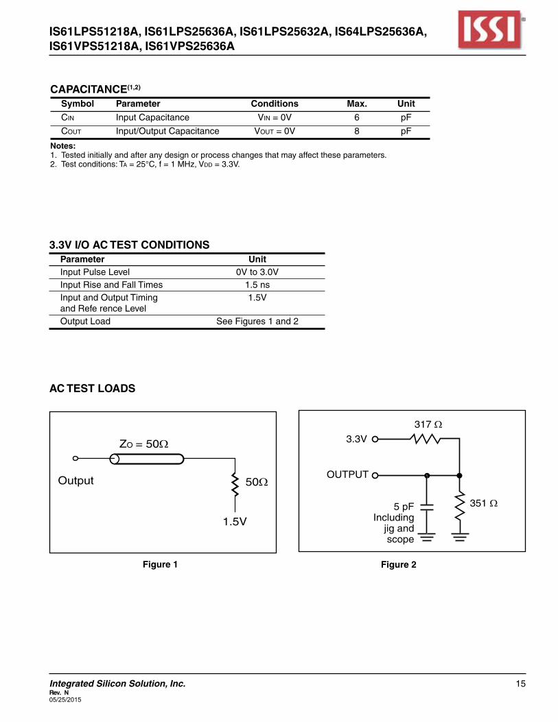
CAPACITANCE(1,2)
Symbol Parameter Conditions Max. Unit
cIN Input Capacitance VIN = 0V 6 pF
cOuT Input/OutputCapacitance VOuT = 0V 8 pF
Notes:1. Testedinitiallyandafteranydesignorprocesschangesthatmayaffecttheseparameters.2. Testconditions:TA = 25°c, f=1MHz,Vdd=3.3V.
3.3V I/O AC TEST CONDITIONS Parameter UnitInputPulseLevel 0Vto3.0VInputRiseandFallTimes 1.5nsInputandOutputTiming 1.5V and Refe rence Level OutputLoad SeeFigures1and2
AC TEST LOADS
Figure 2
317 Ω
5 pFIncluding
jig andscope
351 Ω
OUTPUT
3.3V
Figure 1
Output
ZO = 50Ω
1.5V
50Ω
16 Integrated Silicon Solution, Inc. Rev. N
05/25/2015
IS61LPS51218A, IS61LPS25636A, IS61LPS25632A, IS64LPS25636A,IS61VPS51218A, IS61VPS25636A
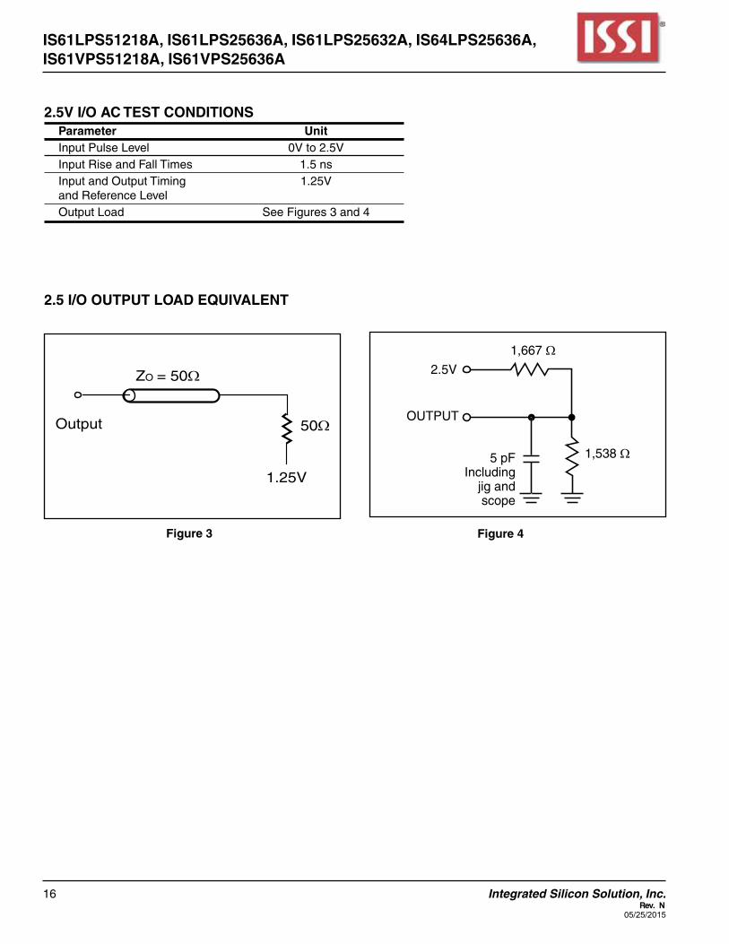
2.5V I/O AC TEST CONDITIONS Parameter Unit InputPulseLevel 0Vto2.5VInputRiseandFallTimes 1.5nsInputandOutputTiming 1.25V and Reference Level OutputLoad SeeFigures3and4
2.5 I/O OUTPUT LOAD EQUIVALENT
Figure 4
1,667 Ω
5 pFIncluding
jig andscope
1,538 Ω
OUTPUT
2.5V
Figure 3
Output
ZO = 50Ω
1.25V
50Ω
17Integrated Silicon Solution, Inc. Rev. N05/25/2015
IS61LPS51218A, IS61LPS25636A, IS61LPS25632A, IS64LPS25636A,IS61VPS51218A, IS61VPS25636A
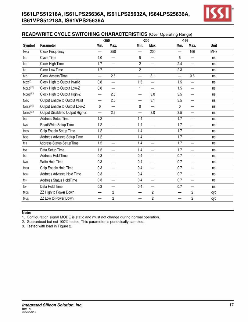
READ/WRITE CYCLE SWITCHINg CHARACTERISTICS (OverOperatingRange) -250 -200 -166
Symbol Parameter Min. Max. Min. Max. Min. Max. Unit
fMAx ClockFrequency — 250 — 200 — 166 MHz
tkc CycleTime 4.0 — 5 — 6 — ns
tkh ClockHighTime 1.7 — 2 — 2.4 — ns
tkl ClockLowTime 1.7 — 2 — 2.3 — ns
tkq ClockAccessTime — 2.6 — 3.1 — 3.8 ns
tkqx(2) ClockHightoOutputInvalid 0.8 — 1.5 — 1.5 — ns
tkqlZ(2,3) ClockHightoOutputLow-Z 0.8 — 1 — 1.5 — ns
tkqhZ(2,3) ClockHightoOutputHigh-Z — 2.6 — 3.0 3.5 — ns
tOEq OutputEnabletoOutputValid — 2.6 — 3.1 3.5 — ns
tOElZ(2,3) OutputEnabletoOutputLow-Z 0 — 0 — 0 — ns
tOEhZ(2,3) OutputDisabletoOutputHigh-Z — 2.6 — 3.0 3.5 — ns
tAs AddressSetupTime 1.2 — 1.4 — 1.7 — ns
tWs Read/WriteSetupTime 1.2 — 1.4 — 1.7 — ns
tcEs ChipEnableSetupTime 1.2 — 1.4 — 1.7 — ns
tAVs AddressAdvanceSetupTime 1.2 — 1.4 — 1.7 — ns
tSs Address Status SetupTime 1.2 — 1.4 — 1.7 — ns
tAh AddressHoldTime 0.3 — 0.4 — 0.7 — ns
tWh WriteHoldTime 0.3 — 0.4 — 0.7 — ns
tcEh ChipEnableHoldTime 0.3 — 0.4 — 0.7 — ns
tAVh AddressAdvanceHoldTime 0.3 — 0.4 — 0.7 — ns
tSH 0.3 — 0.4 — 0.7 — ns
tPds ZZHightoPowerDown — 2 — 2 — 2 cyc
tPus ZZLowtoPowerDown — 2 — 2 — 2 cyc
Note:1. ConfigurationsignalMODEisstaticandmustnotchangeduringnormaloperation.2. Guaranteedbutnot100%tested.Thisparameterisperiodicallysampled.3. TestedwithloadinFigure2.
tds DataSetupTime 1.2 — 1.4 — 1.7 — ns
tdh DataHoldTime 0.3 — 0.4 — 0.7 — ns
Address Status HoldTime

18 Integrated Silicon Solution, Inc. Rev. N
05/25/2015
IS61LPS51218A, IS61LPS25636A, IS61LPS25632A, IS64LPS25636A,IS61VPS51218A, IS61VPS25636A
READ CYCLE TIMINg
Single Read
High-Z
High-ZDATAOUT
DATAIN
OE
CE2
CE2
CE
BWx
BWE
GW
Address
ADV
ADSC
ADSP
CLK
RD1 RD2
1a 2c 2d
UnselectedBurst Read
tKQX
tKC
tKLtKHtSS tSH
tSS tSH
tAS tAH
tWS tWH
tWS tWH
RD3
tCES tCEH
tCES tCEH
tCES tCEH
CE2 and CE2 only sampled with ADSP or ADSC
CE Masks ADSP
Unselected with CE2
tOEQ
tOELZ
tKQLZ
tKQ
tOEHZ
tKQHZ
ADSC initiate read
ADSP is blocked by CE inactive
tAVHtAVS Suspend Burst
Pipelined Read
2a 2b

19Integrated Silicon Solution, Inc.Rev. N05/25/2015
IS61LPS51218A, IS61LPS25636A, IS61LPS25632A, IS64LPS25636A,IS61VPS51218A, IS61VPS25636A
WRITE CYCLE TIMINg
Single Write
DATAOUT
DATAIN
OE
CE2
CE2
CE
BWx
BWE
GW
Address
ADV
ADSC
ADSP
CLK
WR1 WR2
UnselectedBurst Write
tKC
tKLtKHtSS tSH
tAS tAH
tWS tWH
tWS tWH
WR3
tCES tCEH
tCES tCEH
tCES tCEH
CE2 and CE2 only sampled with ADSP or ADSC
CE Masks ADSP
Unselected with CE2
ADSC initiate Write
ADSP is blocked by CE inactive
tAVHtAVSADV must be inactive for ADSP Write
WR1 WR2
tWS tWH
WR3
tWS tWH
High-Z
High-Z 1a 3a
tDS tDH BW4-BW1 only are applied to first cycle of WR2
Write
2c 2d2a 2b
tSS tSH
20 Integrated Silicon Solution, Inc. Rev. N
05/25/2015
IS61LPS51218A, IS61LPS25636A, IS61LPS25632A, IS64LPS25636A,IS61VPS51218A, IS61VPS25636A
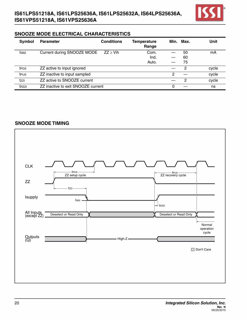
SNOOZE MODE TIMINg
Don't Care
Deselect or Read Only Deselect or Read Only
tRZZI
CLK
ZZ
Isupply
All Inputs (except ZZ)
Outputs (Q)
ISB2
ZZ setup cycle ZZ recovery cycle
Normaloperation
cycle
tPDS tPUS
tZZI
High-Z
SNOOZE MODE ELECTRICAL CHARACTERISTICS
Symbol Parameter Conditions Temperature Min. Max. Unit Range
Isb2 CurrentduringSNOOZEMODE ZZ≥Vih Com. — 50 mAInd. — 60Auto. — 75
tPds ZZactivetoinputignored — 2 cycle
tPus ZZinactivetoinputsampled 2 — cycle
tZZI ZZactivetoSNOOZEcurrent — 2 cycle
trZZI ZZinactivetoexitSNOOZEcurrent 0 — ns
21Integrated Silicon Solution, Inc. Rev. N05/25/2015
IS61LPS51218A, IS61LPS25636A, IS61LPS25632A, IS64LPS25636A,IS61VPS51218A, IS61VPS25636A
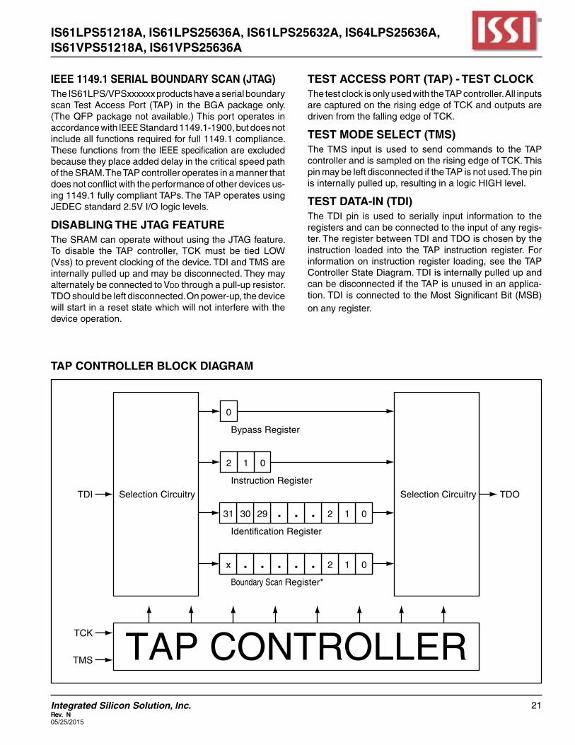
IEEE 1149.1 SERIAL BOUNDARY SCAN (JTAg)TheIS61LPS/VPSxxxxxxproductshaveaserialboundaryscanTestAccessPort (TAP) in theBGApackageonly.(TheQFPpackagenotavailable.)Thisportoperatesinaccordance with IEEEStandard1149.1-1900,butdoesnotincludeallfunctionsrequiredforfull1149.1compliance.ThesefunctionsfromtheIEEEspecificationareexcludedbecause they place added delay in the critical speed path oftheSRAM.TheTAPcontrolleroperatesinamannerthatdoes not conflict with the performance of other devices us-ing1149.1fullycompliantTAPs.TheTAPoperatesusingJEDECstandard2.5VI/Ologiclevels.
DISABLINg THE JTAg FEATURETheSRAMcanoperatewithoutusingtheJTAGfeature.To disable theTAP controller,TCKmust be tied LOW(Vss)topreventclockingofthedevice.TDIandTMSareinternallypulledupandmaybedisconnected.TheymayalternatelybeconnectedtoVddthroughapull-upresistor.TDOshouldbeleftdisconnected.Onpower-up,thedevicewill start in a reset state which will not interfere with the device operation.
TEST ACCESS PORT (TAP) - TEST CLOCKThetestclockisonlyusedwiththeTAPcontroller.AllinputsarecapturedontherisingedgeofTCKandoutputsaredrivenfromthefallingedgeofTCK.
TEST MODE SELECT (TMS)TheTMS input is used to send commands to theTAPcontrollerandissampledontherisingedgeofTCK.ThispinmaybeleftdisconnectediftheTAPisnotused.Thepinisinternallypulledup,resultinginalogicHIGHlevel.
TEST DATA-IN (TDI)TheTDIpin isused to serially input information to theregisters and can be connected to the input of any regis-ter.TheregisterbetweenTDIandTDOischosenbytheinstruction loaded into theTAP instruction register. Forinformationon instructionregister loading,see theTAPControllerStateDiagram.TDIisinternallypulledupandcanbedisconnectediftheTAPisunusedinanapplica-tion.TDIisconnectedtotheMostSignificantBit(MSB)on any register.
31 30 29 . . . 2 1 0
2 1 0
0
x . . . . . 2 1 0
Bypass Register
Instruction Register
Identification Register
Boundary Scan Register*
TAP CONTROLLER
Selection Circuitry Selection Circuitry TDOTDI
TCK
TMS
TAP CONTROLLER BLOCK DIAgRAM
22 Integrated Silicon Solution, Inc. Rev. N
05/25/2015
IS61LPS51218A, IS61LPS25636A, IS61LPS25632A, IS64LPS25636A,IS61VPS51218A, IS61VPS25636A
TEST DATA OUT (TDO)TheTDOoutputpinisusedtoseriallyclockdata-outfromtheregisters.Theoutputisactivedependingonthecurrentstate of the TAP state machine (see TAP Controller State Diagram).TheoutputchangesonthefallingedgeofTCKandTDOisconnectedtotheLeastSignificantBit(LSB)of any register.
PERFORMINg A TAP RESETAResetisperformedbyforcingTMSHIGH(Vdd) for five risingedgesofTCK.RESETmaybeperformedwhiletheSRAMisoperatinganddoesnotaffectitsoperation.Atpower-up,theTAPisinternallyresettoensurethatTDOcomesupinahigh-Zstate.
TAP REgISTERSRegistersareconnectedbetweentheTDIandTDOpinsandallowdatatobescannedintoandoutoftheSRAMtest circuitry. Onlyoneregistercanbeselectedatatimethroughtheinstructionregisters.Dataisserially loadedintotheTDIpinontherisingedgeofTCKandoutputontheTDOpinonthefallingedgeofTCK.
Instruction RegisterThree-bit instructionscanbeseriallyloadedintothein-structionregister.Thisregisterisloadedwhenitisplacedbetween the TDI and TDO pins. (See TAPControllerBlockDiagram) Atpower-up,theinstructionregisterisloadedwith the IDCODE instruction. It is also loadedwith theIDCODEinstructionifthecontrollerisplacedinaresetstate as previously described.
WhentheTAPcontrollerisintheCaptureIRstate,thetwoleastsignificantbitsareloadedwithabinary“01”patterntoallow for fault isolation of the board level serial test path.
Bypass RegisterTosavetimewhenseriallyshiftingdatathroughregisters,itissometimesadvantageoustoskipcertainstates.Thebypassregisterisasingle-bitregisterthatcanbeplacedbetweenTDIandTDOpins.Thisallowsdatatobeshiftedthrough the SRAMwithminimaldelay.Thebypass reg-
ister issetLOW(Vss)when theBYPASS instruction isexecuted.
Boundary Scan RegisterTheboundaryscanregisterisconnectedtoallinputandoutput pins on the SRAM. Several no connect (NC) pins are also included in the scan register to reserve pins for higher densitydevices.Thex36configurationhasa75-bit-longregisterandthex18configurationalsohasa75-bit-longregister.Theboundaryscan register is loadedwith thecontentsoftheRAMInputandOutputringwhentheTAPcontrollerisintheCapture-DRstateandthenplacedbe-tween the TDI and TDO pins when the controller is moved to the Shift-DRstate.TheEXTEST,SAMPLE/PRELOADandSAMPLE-ZinstructionscanbeusedtocapturethecontentsoftheInputandOutputring.
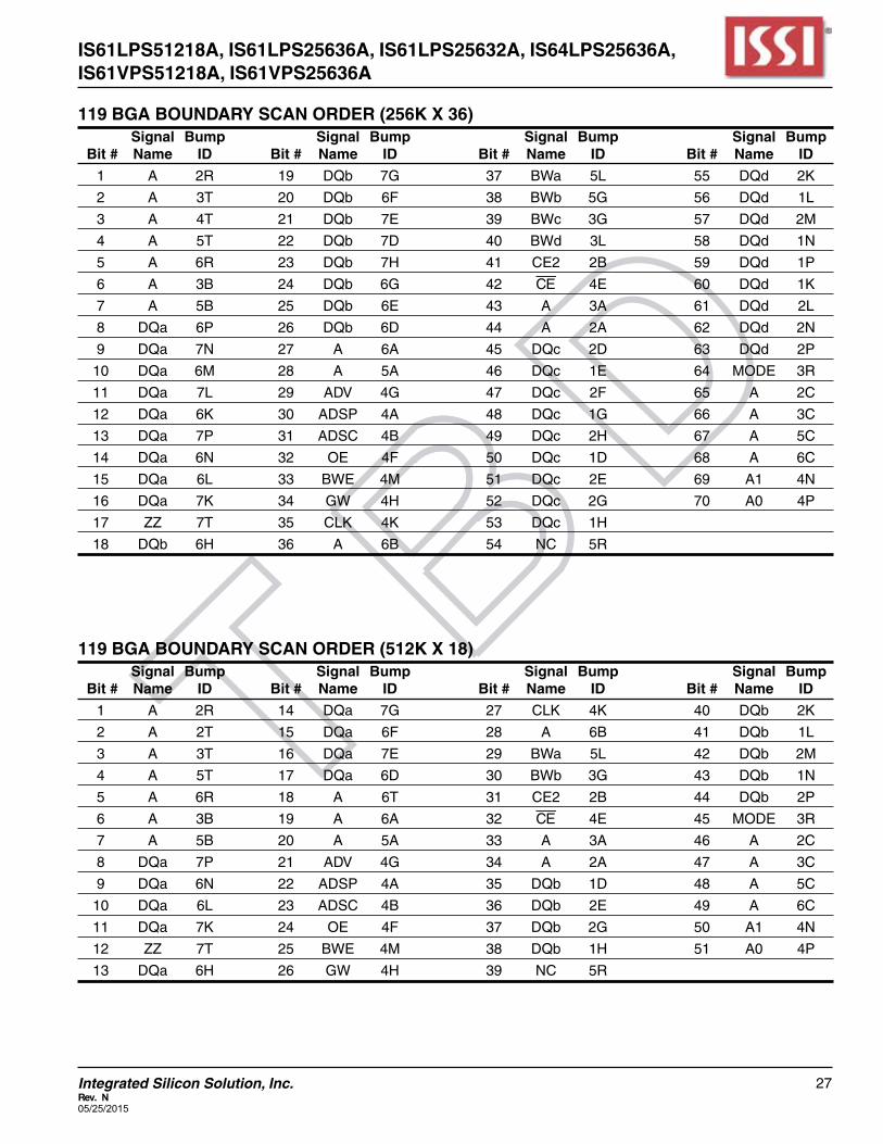
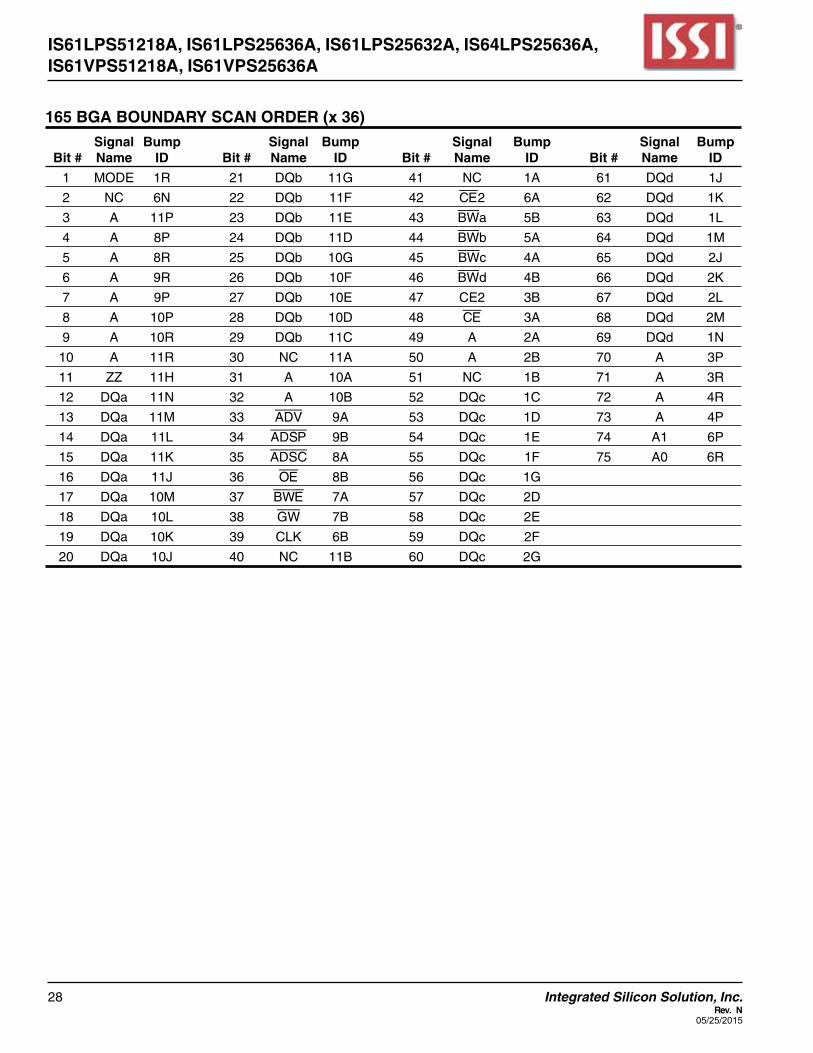
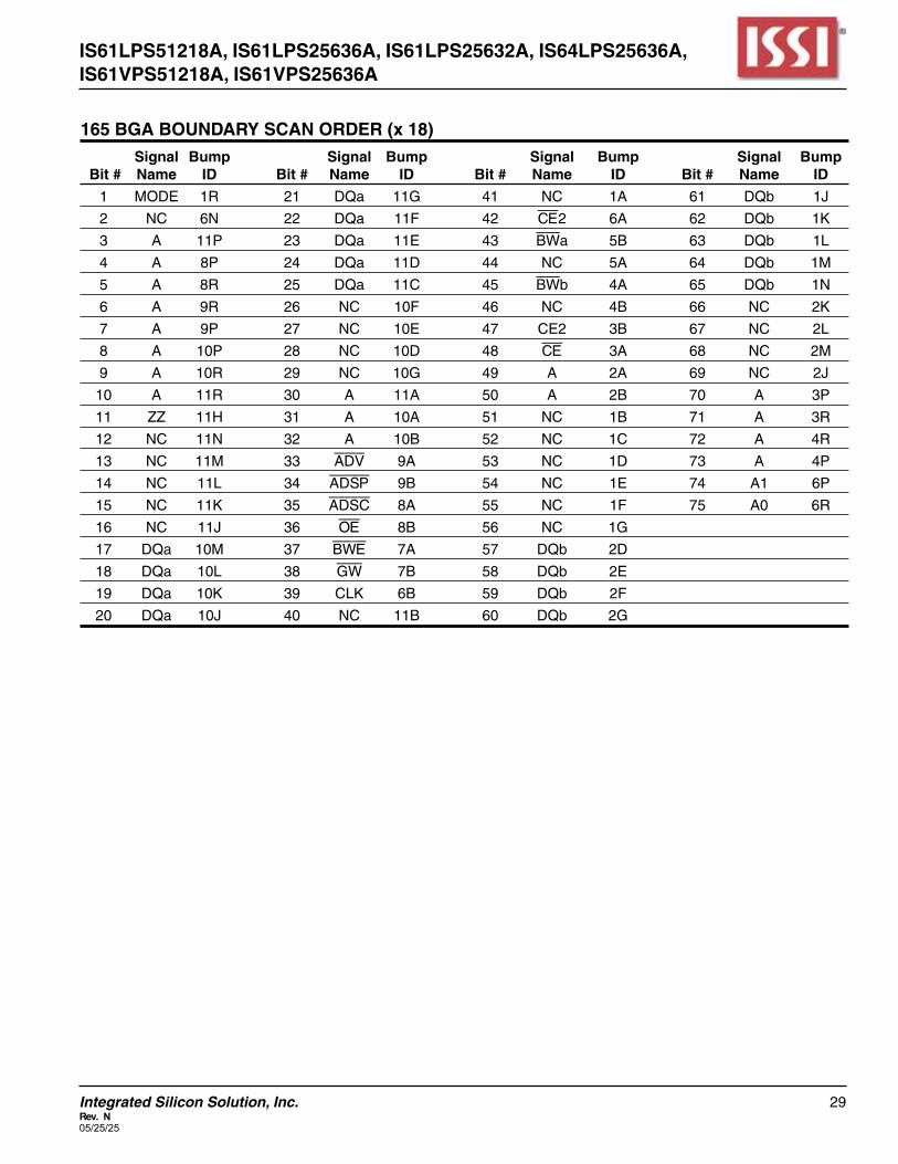
TheBoundaryScanOrdertablesshowtheorderinwhichthebitsareconnected.EachbitcorrespondstooneofthebumpsontheSRAMpackage.TheMSBoftheregisterisconnectedtoTDI,andtheLSBisconnectedtoTDO.
Identification (ID) RegisterThe ID register is loadedwitha vendor-specific, 32-bitcodeduringtheCapture-DRstatewhentheIDCODEcom-mandisloadedtotheinstructionregister.TheIDCODEishardwiredintotheSRAMandcanbeshiftedoutwhentheTAPcontrollerisintheShift-DRstate.TheIDregisterhas vendor code and other information described in the IdentificationRegisterDefinitionstable.
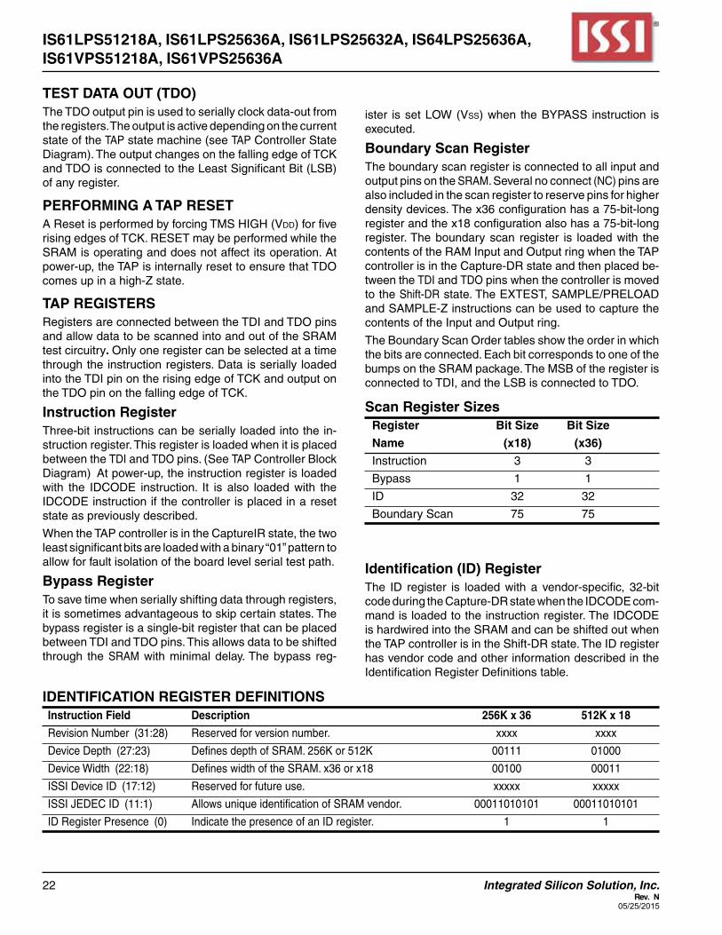
Scan Register SizesRegister Bit Size Bit Size
Name (x18) (x36)
Instruction 3 3
Bypass 1 1
ID 32 32
BoundaryScan 75 75
IDENTIFICATION REgISTER DEFINITIONSInstruction Field Description 256K x 36 512K x 18
RevisionNumber (31:28) Reservedforversionnumber. xxxx xxxx
DeviceDepth (27:23) DefinesdepthofSRAM.256Kor512K 00111 01000
DeviceWidth (22:18) DefineswidthoftheSRAM.x36orx18 00100 00011
ISSIDeviceID (17:12) Reservedforfutureuse. xxxxx xxxxx
ISSIJEDECID (11:1) AllowsuniqueidentificationofSRAMvendor. 00011010101 00011010101
IDRegisterPresence (0) IndicatethepresenceofanIDregister. 1 1
23Integrated Silicon Solution, Inc.Rev. N05/25/2015
IS61LPS51218A, IS61LPS25636A, IS61LPS25632A, IS64LPS25636A,IS61VPS51218A, IS61VPS25636A
TAP INSTRUCTION SETEightinstructionsarepossiblewiththethree-bitinstructionregister and all combinations are listed in the Instruction Code table.Three instructionsare listedasRESERVED and should not be used and the other five instructions are describedbelow.TheTAPcontrollerusedinthisSRAMisnotfullycompliantwiththe1149.1conventionbecausesome mandatory instructions are not fully implemented. TheTAPcontrollercannotbeusedtoloadaddress,dataorcontrol signals and cannot preload the Input or Output buf-fers.TheSRAM does not implement the 1149.1 commands EXTEST or INTEST or the PRELOAD portion of SAMPLE/PRELOAD;insteaditperformsacaptureoftheInputs and Outputringwhentheseinstructionsareexecuted.Instruc-tionsareloadedintotheTAPcontrollerduringtheShift-IRstatewhentheinstructionregisterisplacedbetweenTDIandTDO.Duringthisstate,instructionsareshiftedfromtheinstructionregisterthroughtheTDIandTDOpins.Toexecuteaninstructiononceitisshiftedin,theTAPcontrol-lermustbemovedintotheUpdate-IRstate.
ExTESTEXTESTisamandatory1149.1instructionwhichistobeexecutedwhenevertheinstructionregisterisloadedwithall0s.BecauseEXTESTisnotimplementedintheTAPcontroller, thisdeviceisnot1149.1standardcompliant.TheTAPcontrollerrecognizesanall-0instruction.WhenanEXTESTinstructionisloadedintotheinstructionregister,theSRAMrespondsasifaSAMPLE/PRELOADinstructionhasbeenloaded.Thereisadifferencebetweentheinstruc-tions, unlike the SAMPLE/PRELOADinstruction,EXTESTplacestheSRAMoutputsinaHigh-Zstate.
IDCODEThe IDCODE instruction causes a vendor-specific, 32-bit code to be loaded into the instruction register. It also placestheinstructionregisterbetweentheTDIandTDOpinsandallowstheIDCODEtobeshiftedoutofthedevicewhen theTAPcontrollerenters theShift-DRstate.TheIDCODEinstructionisloadedintotheinstructionregisteruponpower-uporwhenevertheTAPcontrollerisgivenatest logic reset state.
SAMPLE-ZThe SAMPLE-Z instruction causes the boundary scanregistertobeconnectedbetweentheTDIandTDOpinswhentheTAPcontrollerisinaShift-DRstate.ItalsoplacesallSRAMoutputsintoaHigh-Zstate.
SAMPLE/PRELOADSAMPLE/PRELOADisa1149.1mandatoryinstruction.ThePRELOADportionofthisinstructionisnotimplemented,sotheTAPcontrollerisnotfully1149.1compliant.WhentheSAMPLE/PRELOADinstructionisloadedtotheinstruc-tionregisterandtheTAPcontrollerisintheCapture-DRstate, a snapshot of data on the inputs and output pins is captured in the boundary scan register.
ItisimportanttorealizethattheTAPcontrollerclockoper-atesatafrequencyupto10MHz,whiletheSRAMclockrunsmorethananorderofmagnitudefaster.Becauseoftheclockfrequencydifferences,itispossiblethatduringtheCapture-DRstate,aninputoroutputwillunder-goatransition.TheTAPmayattemptasignalcapturewhileintransition(metastablestate).Thedevicewillnotbeharmed,but there is no guarantee of the value that will be captured or repeatable results.
Toguaranteethattheboundaryscanregisterwillcapturethecorrectsignalvalue,theSRAMsignalmustbestabilizedlongenoughtomeettheTAPcontroller’scaptureset-upplus hold times (tcs and tch).ToinsurethattheSRAMclockinput is captured correctly, designs need a way to stop (or slow)theclockduringaSAMPLE/PRELOADinstruction.If this is not an issue, it is possible to capture all other signals and simply ignore the value of the CLK captured in the boundary scan register.
Oncethedataiscaptured,itispossibletoshiftoutthedatabyputtingtheTAPintotheShift-DRstate.ThisplacestheboundaryscanregisterbetweentheTDIandTDOpins.
Note that since the PRELOAD part of the command is not implemented, putting the TAP into the Update to the Update-DR state while performing a SAMPLE/PRELOAD instruction willhavethesameeffectasthePause-DRcommand.
BYPASSWhen theBYPASS instruction is loaded in the instruc-tion registerand theTAP isplaced inaShift-DRstate,thebypassregisterisplacedbetweentheTDIandTDOpins.TheadvantageoftheBYPASSinstructionisthatitshortens the boundary scan path when multiple devices are connected together on a board.
RESERVEDTheseinstructionsarenotimplementedbutarereservedforfutureuse.Donotusetheseinstructions.

24 Integrated Silicon Solution, Inc. Rev. N
05/25/2015
IS61LPS51218A, IS61LPS25636A, IS61LPS25632A, IS64LPS25636A,IS61VPS51218A, IS61VPS25636A
INSTRUCTION CODES Code Instruction Description
000 EXTEST CapturestheInput/Outputringcontents.Placestheboundaryscanregisterbe-tweentheTDIandTDO.ForcesallSRAMoutputstoHigh-Zstate.This instructionisnot1149.1compliant.
001 IDCODE LoadstheIDregisterwiththevendorIDcodeandplacestheregisterbetweenTDIandTDO.ThisoperationdoesnotaffectSRAMoperation.
010 SAMPLE-Z CapturestheInput/Outputcontents.PlacestheboundaryscanregisterbetweenTDIandTDO.ForcesallSRAMoutputdriverstoaHigh-Zstate.
011 RESERVED DoNotUse:Thisinstructionisreservedforfutureuse.
100 SAMPLE/PRELOAD CapturestheInput/Outputringcontents.Placestheboundaryscanregisterbetween TDIandTDO.DoesnotaffecttheSRAMoperation.Thisinstructiondoesnotimplement1149.1preloadfunctionandisthereforenot1149.1compliant.
101 RESERVED DoNotUse:Thisinstructionisreservedforfutureuse.
110 RESERVED DoNotUse:Thisinstructionisreservedforfutureuse.
111 BYPASS PlacesthebypassregisterbetweenTDIandTDO.Thisoperationdoesnot affectSRAMoperation.
Select DR
Capture DR
Shift DR
Exit1 DR
Pause DR
Exit2 DR
Update DR
Select IR
Capture IR
Shift IR
Exit1 IR
Pause IR
Exit2 IR
Update IR
Test Logic Reset
Run Test/Idle1 1 1
1 1
1 1
1
1
11
11
1
0
0
0
0
1
0 0
0
0
0
0
0
0
0
0
0
1 0
TAP CONTROLLER STATE DIAgRAM
25Integrated Silicon Solution, Inc.Rev. N05/25/2015
IS61LPS51218A, IS61LPS25636A, IS61LPS25632A, IS64LPS25636A,IS61VPS51218A, IS61VPS25636A
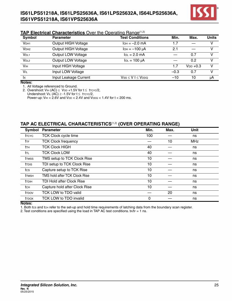
TAP Electrical Characteristics OvertheOperatingRange(1,2)
Symbol Parameter Test Conditions Min. Max. Units
VOh1 OutputHIGHVoltage IOh=–2.0mA 1.7 — V
VOh2 OutputHIGHVoltage IOh=–100µA 2.1 — V
VOl1 OutputLOWVoltage IOl=2.0mA — 0.7 V
VOl2 OutputLOWVoltage IOl=100µA — 0.2 V
VIh InputHIGHVoltage 1.7 Vdd+0.3 V
VIl InputLOWVoltage –0.3 0.7 V
Ix Input Leakage Current Vss ≤VI≤Vddq –10 10 µANotes:1. AllVoltagereferencedtoGround.2. Overshoot:VIh (AC) ≤Vdd+1.5Vfort≤ tTcyc/2,Undershoot:VIl (AC) ≥ -1.5Vfort≤ tTcyc/2,Power-up:VIh<2.6VandVdd<2.4VandVddq<1.4Vfort<200ms.
TAP AC ELECTRICAL CHARACTERISTICS(1,2) (OVER OPERATINg RANgE) Symbol Parameter Min. Max. Unit
tTcyc TCKClockcycletime 100 — ns
fTf TCKClockfrequency — 10 MHz
tTh TCKClockHIGH 40 — ns
tTl TCKClockLOW 40 — ns
tTMss TMSsetuptoTCKClockRise 10 — ns
tTdIs TDIsetuptoTCKClockRise 10 — ns
tcs CapturesetuptoTCKRise 10 — ns
tTMsh TMSholdafterTCKClockRise 10 — ns
tTdIh TDIHoldafterClockRise 10 — ns
tch Capture hold after Clock Rise 10 — ns
tTdOV TCKLOWtoTDOvalid — 20 ns
tTdOx TCKLOWtoTDOinvalid 0 — nsNotes:1.Bothtcs and tch refertotheset-upandholdtimerequirementsoflatchingdatafromtheboundaryscanregister.2.TestconditionsarespecifiedusingtheloadinTAPACtestconditions.tr/tf=1ns.
26 Integrated Silicon Solution, Inc. Rev. N
05/25/2015
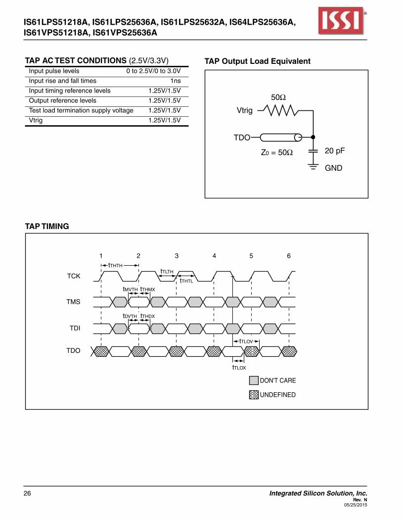
IS61LPS51218A, IS61LPS25636A, IS61LPS25632A, IS64LPS25636A,IS61VPS51218A, IS61VPS25636A
DON'T CARE
UNDEFINED
TCK
TMS
TDI
TDO
tTHTL
tTLTHtTHTH
tMVTH tTHMX
tDVTH tTHDX
1 2 3 4 5 6
tTLOX
tTLOV
TAP TIMINg
20 pF
TDO
GND
50Ω
Vtrig
Z0 = 50Ω
TAP Output Load EquivalentTAP AC TEST CONDITIONS (2.5V/3.3V)Inputpulselevels 0to2.5V/0to3.0V
Input rise and fall times 1ns
Inputtimingreferencelevels 1.25V/1.5V
Outputreferencelevels 1.25V/1.5V
Testloadterminationsupplyvoltage 1.25V/1.5V
Vtrig 1.25V/1.5V
27Integrated Silicon Solution, Inc. Rev. N05/25/2015
IS61LPS51218A, IS61LPS25636A, IS61LPS25632A, IS64LPS25636A,IS61VPS51218A, IS61VPS25636A
119 BgA BOUNDARY SCAN ORDER (256K x 36)Signal Bump Signal Bump Signal Bump Signal Bump
Bit # Name ID Bit # Name ID Bit # Name ID Bit # Name ID
1 A 2R 19 DQb 7G 37 BWa 5L 55 DQd 2K
2 A 3T 20 DQb 6F 38 BWb 5G 56 DQd 1L
3 A 4T 21 DQb 7E 39 BWc 3G 57 DQd 2M
4 A 5T 22 DQb 7D 40 BWd 3L 58 DQd 1N
5 A 6R 23 DQb 7H 41 CE2 2B 59 DQd 1P
6 A 3B 24 DQb 6G 42 CE 4E 60 DQd 1K
7 A 5B 25 DQb 6E 43 A 3A 61 DQd 2L
8 DQa 6P 26 DQb 6D 44 A 2A 62 DQd 2N
9 DQa 7N 27 A 6A 45 DQc 2D 63 DQd 2P
10 DQa 6M 28 A 5A 46 DQc 1E 64 MODE 3R
11 DQa 7L 29 ADV 4G 47 DQc 2F 65 A 2C
12 DQa 6K 30 ADSP 4A 48 DQc 1G 66 A 3C
13 DQa 7P 31 ADSC 4B 49 DQc 2H 67 A 5C
14 DQa 6N 32 OE 4F 50 DQc 1D 68 A 6C
15 DQa 6L 33 BWE 4M 51 DQc 2E 69 A1 4N
16 DQa 7K 34 GW 4H 52 DQc 2G 70 A0 4P
17 ZZ 7T 35 CLK 4K 53 DQc 1H
18 DQb 6H 36 A 6B 54 NC 5R
119 BgA BOUNDARY SCAN ORDER (512K x 18)Signal Bump Signal Bump Signal Bump Signal Bump
Bit # Name ID Bit # Name ID Bit # Name ID Bit # Name ID
1 A 2R 14 DQa 7G 27 CLK 4K 40 DQb 2K
2 A 2T 15 DQa 6F 28 A 6B 41 DQb 1L
3 A 3T 16 DQa 7E 29 BWa 5L 42 DQb 2M
4 A 5T 17 DQa 6D 30 BWb 3G 43 DQb 1N
5 A 6R 18 A 6T 31 CE2 2B 44 DQb 2P
6 A 3B 19 A 6A 32 CE 4E 45 MODE 3R
7 A 5B 20 A 5A 33 A 3A 46 A 2C
8 DQa 7P 21 ADV 4G 34 A 2A 47 A 3C
9 DQa 6N 22 ADSP 4A 35 DQb 1D 48 A 5C
10 DQa 6L 23 ADSC 4B 36 DQb 2E 49 A 6C
11 DQa 7K 24 OE 4F 37 DQb 2G 50 A1 4N
12 ZZ 7T 25 BWE 4M 38 DQb 1H 51 A0 4P
13 DQa 6H 26 GW 4H 39 NC 5R
28 Integrated Silicon Solution, Inc. Rev. N
05/25/2015
IS61LPS51218A, IS61LPS25636A, IS61LPS25632A, IS64LPS25636A,IS61VPS51218A, IS61VPS25636A
165 BgA BOUNDARY SCAN ORDER (x 36)
Signal Bump Signal Bump Signal Bump Signal Bump Bit # Name ID Bit # Name ID Bit # Name ID Bit # Name ID
1 MODE 1R 21 DQb 11G 41 NC 1A 61 DQd 1J
2 NC 6N 22 DQb 11F 42 CE2 6A 62 DQd 1K
3 A 11P 23 DQb 11E 43 BWa 5B 63 DQd 1L
4 A 8P 24 DQb 11D 44 BWb 5A 64 DQd 1M
5 A 8R 25 DQb 10G 45 BWc 4A 65 DQd 2J
6 A 9R 26 DQb 10F 46 BWd 4B 66 DQd 2K
7 A 9P 27 DQb 10E 47 CE2 3B 67 DQd 2L
8 A 10P 28 DQb 10D 48 CE 3A 68 DQd 2M
9 A 10R 29 DQb 11C 49 A 2A 69 DQd 1N
10 A 11R 30 NC 11A 50 A 2B 70 A 3P
11 ZZ 11H 31 A 10A 51 NC 1B 71 A 3R
12 DQa 11N 32 A 10B 52 DQc 1C 72 A 4R
13 DQa 11M 33 ADV 9A 53 DQc 1D 73 A 4P
14 DQa 11L 34 ADSP 9B 54 DQc 1E 74 A1 6P
15 DQa 11K 35 ADSC 8A 55 DQc 1F 75 A0 6R
16 DQa 11J 36 OE 8B 56 DQc 1G
17 DQa 10M 37 BWE 7A 57 DQc 2D
18 DQa 10L 38 GW 7B 58 DQc 2E
19 DQa 10K 39 CLK 6B 59 DQc 2F
20 DQa 10J 40 NC 11B 60 DQc 2G
29Integrated Silicon Solution, Inc.Rev. N05/25/25
IS61LPS51218A, IS61LPS25636A, IS61LPS25632A, IS64LPS25636A,IS61VPS51218A, IS61VPS25636A
165 BgA BOUNDARY SCAN ORDER (x 18)
Signal Bump Signal Bump Signal Bump Signal Bump Bit # Name ID Bit # Name ID Bit # Name ID Bit # Name ID
1 MODE 1R 21 DQa 11G 41 NC 1A 61 DQb 1J
2 NC 6N 22 DQa 11F 42 CE2 6A 62 DQb 1K
3 A 11P 23 DQa 11E 43 BWa 5B 63 DQb 1L
4 A 8P 24 DQa 11D 44 NC 5A 64 DQb 1M
5 A 8R 25 DQa 11C 45 BWb 4A 65 DQb 1N
6 A 9R 26 NC 10F 46 NC 4B 66 NC 2K
7 A 9P 27 NC 10E 47 CE2 3B 67 NC 2L
8 A 10P 28 NC 10D 48 CE 3A 68 NC 2M
9 A 10R 29 NC 10G 49 A 2A 69 NC 2J
10 A 11R 30 A 11A 50 A 2B 70 A 3P
11 ZZ 11H 31 A 10A 51 NC 1B 71 A 3R
12 NC 11N 32 A 10B 52 NC 1C 72 A 4R
13 NC 11M 33 ADV 9A 53 NC 1D 73 A 4P
14 NC 11L 34 ADSP 9B 54 NC 1E 74 A1 6P
15 NC 11K 35 ADSC 8A 55 NC 1F 75 A0 6R
16 NC 11J 36 OE 8B 56 NC 1G
17 DQa 10M 37 BWE 7A 57 DQb 2D
18 DQa 10L 38 GW 7B 58 DQb 2E
19 DQa 10K 39 CLK 6B 59 DQb 2F
20 DQa 10J 40 NC 11B 60 DQb 2G
30 Integrated Silicon Solution, Inc. Rev. N
05/25/2015
IS61LPS51218A, IS61LPS25636A, IS61LPS25632A, IS64LPS25636A,IS61VPS51218A, IS61VPS25636A
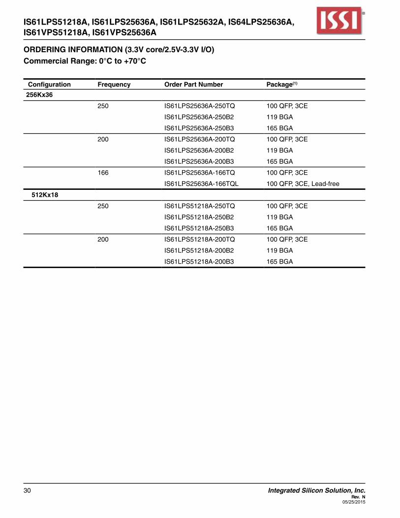
Configuration Frequency Order Part Number Package(1)
256Kx36
250 IS61LPS25636A-250TQ 100QFP,3CE
IS61LPS25636A-250B2 119BGA
IS61LPS25636A-250B3 165BGA
200 IS61LPS25636A-200TQ 100QFP,3CE
IS61LPS25636A-200B2 119BGA
IS61LPS25636A-200B3 165BGA
166 IS61LPS25636A-166TQ 100QFP,3CE
IS61LPS25636A-166TQL 100QFP,3CE,Lead-free
512Kx18
250 IS61LPS51218A-250TQ 100QFP,3CE
IS61LPS51218A-250B2 119BGA
IS61LPS51218A-250B3 165BGA
200 IS61LPS51218A-200TQ 100QFP,3CE
IS61LPS51218A-200B2 119BGA
IS61LPS51218A-200B3 165BGA
ORDERINg INFORMATION (3.3V core/2.5V-3.3V I/O)Commercial Range: 0°C to +70°C

31Integrated Silicon Solution, Inc.Rev. N05/25/2015
IS61LPS51218A, IS61LPS25636A, IS61LPS25632A, IS64LPS25636A,IS61VPS51218A, IS61VPS25636A
Automotive Range: -40°C to +125°C Configuration Frequency Order Part Number Package
256Kx36
166 IS64LPS25636A-166TQLA3 100QFP,3CE
Configuration Frequency OrderPartNumber Package(1)
256Kx32
200 IS61LPS25632A-200TQLI 100QFP,3CE,Lead-free
256Kx36
250 IS61LPS25636A-250TQI 100QFP,3CE
IS61LPS25636A-250TQLI 100QFP,3CE,Lead-free
IS61LPS25636A-250B2I 119BGA
IS61LPS25636A-250B3I 165BGA
200 IS61LPS25636A-200TQI 100QFP,3CE
IS61LPS25636A-200TQ2LI 100QFP,2CE,Lead-free
IS61LPS25636A-200TQ2I 100QFP,2CE
IS61LPS25636A-200TQLI 100QFP,3CE,Lead-free
IS61LPS25636A-200B2I 119BGA
IS61LPS25636A-200B2LI 119BGA,Lead-free
IS61LPS25636A-200B3I 165BGA
166 IS61LPS25636A-200B3LI 165BGA,Lead-free
512Kx18
250 IS61LPS51218A-250TQI 100QFP,3CE
IS61LPS51218A-250B2I 119BGA
IS61LPS51218A-250B3I 165BGA
200 IS61LPS51218A-200TQI 100QFP,3CE
IS61LPS51218A-200TQ2LI 100QFP,2CE,Lead-free
IS61LPS51218A-200TQ2I 100QFP,2CE
IS61LPS51218A-200TQLI 100QFP,3CE,Lead-free
IS61LPS51218A-200B2I 119BGA
IS61LPS51218A-200B3I 165BGA
Note:1. For100QFP,[email protected]
Industrial Range: -40°C to +85°C

32 Integrated Silicon Solution, Inc. Rev. N
05/25/2015
IS61LPS51218A, IS61LPS25636A, IS61LPS25632A, IS64LPS25636A,IS61VPS51218A, IS61VPS25636A
ORDERINg INFORMATION (2.5V core/2.5V I/O)Commercial Range: 0°C to +70°C Configuration Frequency Order Part Number Package(1)
256Kx36
250 IS61VPS25636A-250TQ 100QFP,3CE IS61VPS25636A-250B2 119BGA
IS61VPS25636A-250B3 165BGA
200 IS61VPS25636A-200TQ 100QFP,3CE IS61VPS25636A-200B2 119BGA
IS61VPS25636A-200B3 165BGA
512Kx18
250 IS61VPS51218A-250TQ 100QFP,3CE IS61VPS51218A-250B2 119BGA
IS61VPS51218A-250B3 165BGA
200 IS61VPS51218A-200TQ 100QFP,3CE IS61VPS51218A-200B2 119BGA
IS61VPS51218A-200B3 165BGA
Industrial Range: -40°C to +85°C Configuration Frequency Order Part Number Package(1)
256Kx36
250 IS61VPS25636A-250TQI 100QFP,3CE IS61VPS25636A-250B2I 119BGA
IS61VPS25636A-250B3I 165BGA
200 IS61VPS25636A-200TQI 100QFP,3CE IS61VPS25636A-200TQ2I 100QFP,2CE IS61VPS25636A-200TQLI 100QFP,3CE,Lead-free IS61VPS25636A-200B2I 119BGA
IS61VPS25636A-200B3I 165BGA
512Kx18
250 IS61VPS51218A-250TQI 100QFP,3CE IS61VPS51218A-250B2I 119BGA
IS61VPS51218A-250B3I 165BGA
200 IS61VPS51218A-200TQI 100QFP,3CEIS61VPS51218A-200TQ2I 100QFP,2CE IS61VPS51218A-200B2I 119BGA
IS61VPS51218A-200B3I 165BGANote:1. For100QFP,[email protected]
33Integrated Silicon Solution, Inc.Rev. N05/25/2015
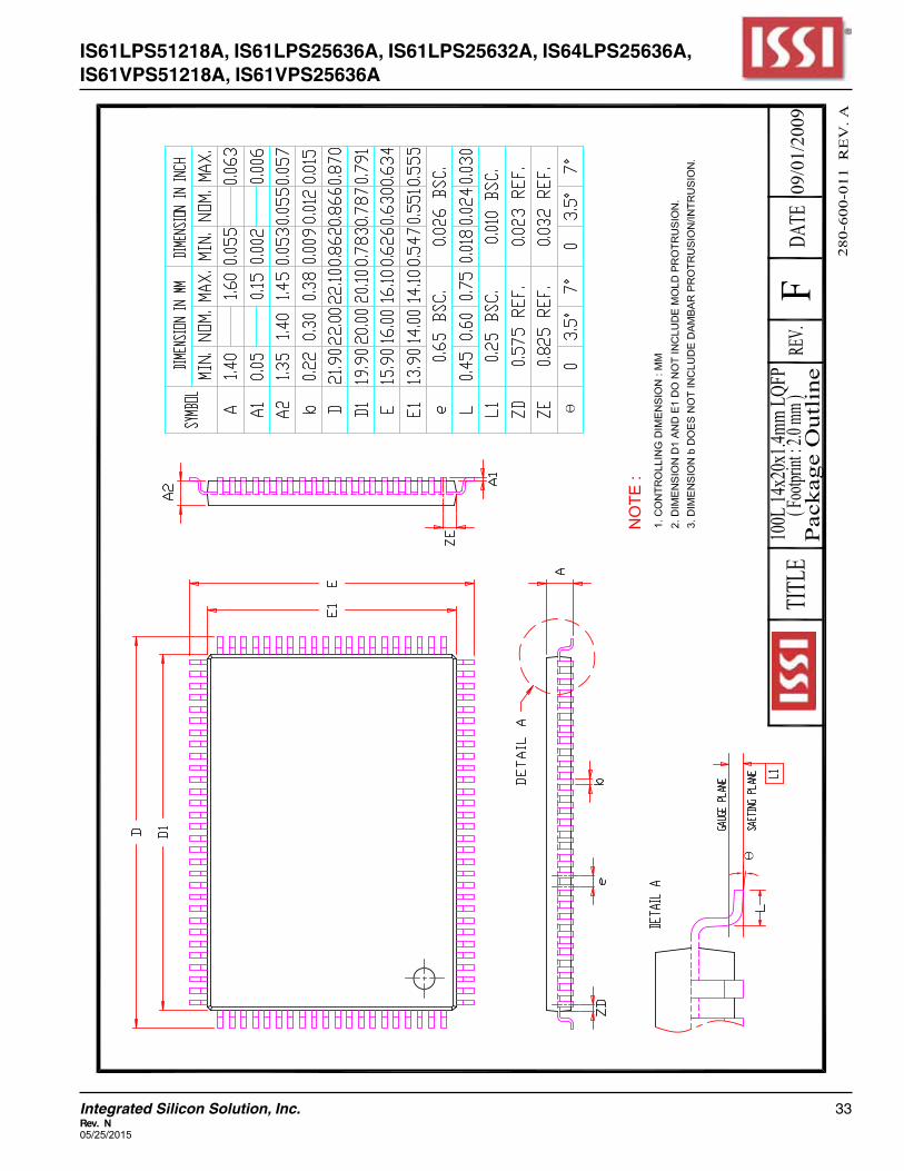
IS61LPS51218A, IS61LPS25636A, IS61LPS25632A, IS64LPS25636A,IS61VPS51218A, IS61VPS25636A

34 Integrated Silicon Solution, Inc. Rev. N
05/25/2015
IS61LPS51218A, IS61LPS25636A, IS61LPS25632A, IS64LPS25636A,IS61VPS51218A, IS61VPS25636A
1.C
ON
TRO
LLIN
G D
IME
NS
ION
: M
M .
NO
TE :
2.R
efer
ence
doc
umen
t : J
ED
EC
MS
-028
10/0
2/20
08Pa
ckag
e O
utlin
e
35Integrated Silicon Solution, Inc.Rev. N05/25/2015
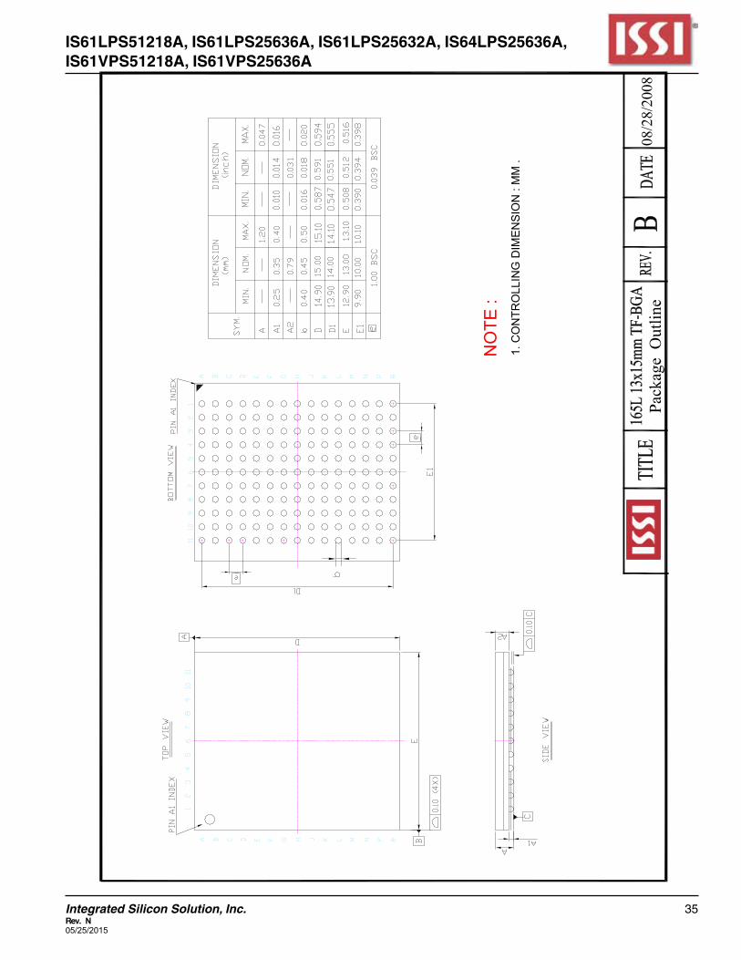
IS61LPS51218A, IS61LPS25636A, IS61LPS25632A, IS64LPS25636A,IS61VPS51218A, IS61VPS25636A
1.C
ON
TRO
LLIN
G D
IME
NS
ION
: M
M .
NO
TE :
Pack
age
Out
line
08/2
8/20
08