Embed Size (px)
Citation preview

2DP4: Microprocessor Systems
Final Project
Instructor: Dr.Doyle
Muhammad Tareen - L07- tareenmj-1313887
As a future member of the engineering profession, the student is responsible for
performing the required work in an honest manner, without plagiarism and
cheating. Submitting this work with my name and student number is a statement
and understanding that this work is my own and adheres to the Academic Integrity
Policy of McMaster University and the Code of Conduct of the Professional
Engineers of Ontario. Submitted by [Muhammad Tareen, tareenmj, 1313887].

Table of Contents
(1) Abstract
(2) Introduction
(3) System Overview
(a) Quantifying Signal Properties
(b) Transducer
(c) Input
(d) Pre-condition Circuit
(e) Esduino Extreme (ESDX) and ADC
(f) Data Processing and Serial Communication
(4) Results
(5) Discussion
(6) Conclusion
(7) Appendix

1: Abstract
The objective of this project was to build a signal acquisition system, as well as
display the signal on a PC. A pre-condition circuit was used to amplify the signal
received from the function generator. Following this, the Esduino Extreme (ESDX)
had to perform Analog-to-Digital conversion, and serially transmit the data to a
program, MatLab. To verify whether or not the system was performing on par, the
oscilloscope and PSpice were used. The waveforms, which were given attention to,
were the sine, square, and saw-tooth waves. They were tested under different
frequencies, 10% of the Nyquist rate, 50% of the Nyquist rate, and 100% of the
Nyquist rate.

2: Introduction
The most integral part of the 21st century is arguably the computer. Computers are
all around us, enriching our lives by tackling the simplest of tasks, like a toaster, to
complex medical equipment, such as an MRI. A fundamental quality of computers, is
to acquire data from their surroundings and manipulate said data; data acquisition.
Data acquisition lays the foundation for computers interacting with the world. Data
acquisition is used to convert information from the analog world to a computer’s
digital one. It is the process of sampling signals measuring real life physical
quantities, such as temperature or pressure, to digital values that can be used by a
computer. The implications of data acquisition seem endless.
This project will exhibit how to use the ESDX microcontroller to perform Analog-to-
Digital conversion, ADC, and how to establish a serial communication (SCI). ADC and
SCI are the two major steps of data acquisition. ADC receives an analog signal and
converts it into a digital format. SCI communicates and displays the converted
analog signal to a program on any computer. Matlab was selected as the program to
display the signal, since it is optimized for displaying waves and signals. The
technique used in ADC is the successive approximation technique, a technique
capable of converting at a very fast rate.
This report goes into a detailed explanation of every step into successively
performing ADC and SCI. Section three will go through a thorough description of the
system overview required for this project. Results and findings are presented in
Section four. Matlab output graphs of the analog signal and outputs from the
oscilloscope of the pre condition circuit are given. Significant questions are
answered in Section five of this report, such as the quantization error, the bus speed,
the limitations of this project, are all discussed. Section six wraps up this project by
giving a concise summary.
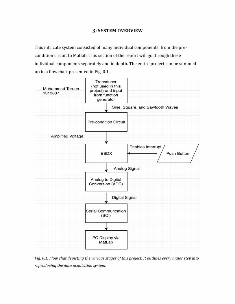
3: SYSTEM OVERVIEW
This intricate system consisted of many individual components, from the pre-
condition circuit to Matlab. This section of the report will go through these
individual components separately and in depth. The entire project can be summed
up in a flowchart presented in Fig. 0.1.
Fig. 0.1: Flow chat depicting the various stages of this project. It outlines every major step into
reproducing the data acquisition system.

(a) Quantifying Signal Properties
Amplitude is the objective measurement of the degree of change, whether it is
positive or negative, over a single period of time.
Frequency is defined to be the rate at which something occurs or repeats over a
period of time
A source is a component in an electrical circuit, which provides electrical energy to
the circuit. A function generator can behave as a source for the circuit, and is the
source for this circuit.
(b) Transducer
A transducer is a component, which converts a physical phenomenon into an
electrical signal. This project had a direct input of an electrical analog voltage, thus
removing any need for a transducer.
(c) Input
A function generator was used to generate an analog signal. The specifications for
the function generator were: a 4 V peak-to-peak voltage, a 0V Direct Current offset,
and a frequency lower than the Nyquist rate (220Hz). This input from the function
generator was directly connected to the pre-condition circuit. As mentioned
previously, the function generator behaved as the source for the circuit.

(d) Pre-Condition Circuit
The pre-condition circuit was required to amplify the analog signal obtained from
the function generator. A physical setup of the circuit is given in Fig. 0.2.
Fig. 0.2: The physical setup of the circuit is given. A push button, resistors, operational
amplifier are incorporated into the circuit.
As seen in Fig. 0.2, the circuit is constructed on a breadboard for testing. Resistor
values of 10kΩ were chosen for R1, two 10kΩ resistors were in parallel followed by
a series connection with another 10kΩ resistor to establish a resistance of 15kΩ for
R2, a one kΩ resistor in series with a 100 Ω to establish a combined resistance of
1.1kΩ for R3, and finally a 1kΩ resistor for R4. Voltages of 3V and 5V were extended
from the Esduino Extreme (ESDX). The 5V was connected to the operational
amplifier, and the 3V was the supply voltage of the circuit. A ground connection was
also made from the ESDX.
Fig. 0.3 represents the pre-condition circuit on Pspice.

Fig. 0.3: The pre-condition circuit represented through the virtual circuit constructor, Pspice.
V1 is the input from the ESDX and V2 is the input from the function generator.
The operational amplifier used was contained in a chip (LMC662 CMOS Dual
Operational Amplifier), the pin layout is given in Fig. 0.4. Only the A side was used
for this project, and thus only pins 1,2,3,4, and 8.
Fig. 0.4: Pin Layout of the Operational Amplifier used in the circuit. The 5V from the ESDX was
connected to pin 8.
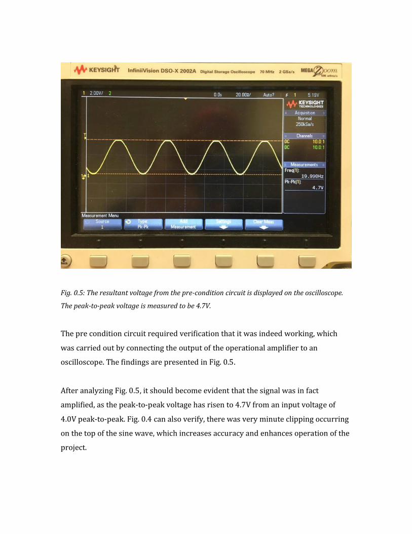
Fig. 0.5: The resultant voltage from the pre-condition circuit is displayed on the oscilloscope.
The peak-to-peak voltage is measured to be 4.7V.
The pre condition circuit required verification that it was indeed working, which
was carried out by connecting the output of the operational amplifier to an
oscilloscope. The findings are presented in Fig. 0.5.
After analyzing Fig. 0.5, it should become evident that the signal was in fact
amplified, as the peak-to-peak voltage has risen to 4.7V from an input voltage of
4.0V peak-to-peak. Fig. 0.4 can also verify, there was very minute clipping occurring
on the top of the sine wave, which increases accuracy and enhances operation of the
project.
(e) Esduino Extreme (ESDX) and ADC
The Esduino Extreme (ESDX) is an Arduino-style board based on FreeScale S12
Microcontrollers. The ESDX is developed and manufactured by Technological Arts.
The ESDX contains a 240K Flash, 4K EEPROM, and 11K RAM memories, SCI, SPI, as
well as CAN communications subsystems, dual 8bit DACs, 8 channel, 16-bit
enhanced timers, on-chip temperature sensors, up to 128 hardware interrupt
sources, I/O port lines, and a 3.3V or 5V operating voltage range. The ESDX has
several pins, designated for unique purposes. The ESDX has multi channel 12-bit
ADC conversion capability. The ESDX has an 8MHz crystal, providing a 4MHz
nominal bus speed, when enabled. The ESDX operates at a 6.25Mhz start up bus
speed. The ESDX was purchased from the IEEE office of McMaster University (ITB-
141), for a price of 100 Canadian Dollars. Since EsduinoXtreme is based on S12, your
code can be developed using any available S12 tools (e.g. CodeWarrior, AsmIDE, C,
GCC, ICC12, Cosmic, etc.).
The overview on how the ESDX makes use of the analog signal and displays it is
given in Fig. 0.6. Four pins of the ESDX were used: AN3 as the channel for ADC, D2 as
an interrupt pin, the 5V supply, the 3V supply, and the GND pin. The push button
from the pre-condition circuit was implemented to start the process of ADC. The
push button was connected to the D2 of the ESDX. Pin D2 serves as an interrupt, and
when it is pressed, the ESDX follows the process outlined in Fig. 0.5. The
requirements for this system were a 440Hz-sampling rate, a 2MHz bus clock speed,
a 12-bit ADC, and an ADC channel of AN3. For this system, the analog signal was
connected to the AN3 pin, and 12-bit ADC was implemented. As mentioned before
the ESDX performs successive approximation, which converts the analog signal to
discrete data. The analog signal received from the pre condition circuit had a peak-
to-peak voltage of approximately 5V. ADC continuously sampled it to get digital
values, representing the signal, and the step size was calculated to be 0.000122V.

Fig. 0.6: The overview of how the ESDX does ADC and transmits the output to Matlab. Only
after the push button is pressed is this procedure started.

% ADC
(12-bit presented in decimal system)
Analog Voltage
(from signal)
100 4096 5
75 3072 3.75
50 2048 2.5
25 1024 1.25
0 0 0
Fig. 0.7: The table for the ADC is presented. Note that only values for 0%, 25%, 50%, 75% and
100% are given.
Fig. 0.7 presents the ADC table for notable values.
Following ADC, the signal received had to be serially transmitted to Matlab from the
CodeWarrior IDE. The baud rate was selected as 9600.
(f) Data Processing and Serial Communication
Following ADC, the signal being received from the ESDX had to be displayed on a graph on a PC from Matlab. The computer used for this entire project was A Macbook Pro with specifications of: 2.6 GHz Intel Core i5, 8GB Memory, OS X El Capitan. The Matlab software was the R2014b edition. Port ‘COM4’ was used for SCI.

4: Results
This portion of the project displays the results of the project, as well as giving
insight on why they were important and why they needed to be included.
(a) Results of Pre-condition Circuit
The Pre-condition circuit was already discussed in System Overview. To verify if it
was working accurately, the output from the operational amplifier was connected to
an oscilloscope to display the analog signal. It is presented in Fig. 0.5.
As presented in Fig. 0.4, the peak-to-peak Voltage is 4.7V. This output voltage was
due to the operational amplifier, amplifying an input peak-to-peak voltage of 4.0V.
Results of the pre-condition circuit were discussed in depth previously. Since there
is barely any clipping occurring, and the input voltage has been amplified, it is
satisfactory to conclude that the pre-condition circuit is working according to the
specifications on it.

(b) MatLab Results
Matlab was the software selected to display the analog signal, after processing from
the ESDX. Matlab displayed the signal for various frequencies at different
waveforms, some more accurate than others.
The graph for 10% of the Nyquist Rate is presented in Fig. 0.8 below.
Fig. 0.8: The output graph from Matlab at 10% of the Nyquist Rate of a sine waveform. The
graph can be seen to extend from approximately 0V to 5V.
Fig. 0.8 displays the graph for 10% of the Sampling frequency (22Hz). The graph
appears to be smooth. It also has a peak-to-peak voltage of approximately 4.5V,
which is very close to our output from the oscilloscope in Fig. 0.5.

The graph for 10% of the Nyquist rate of a triangle waveform is given in Fig. 0.9.
Fig. 0.9: The output graph from Matlab at 10% of the Nyquist Rate of a triangle waveform. The
graph can be seen to extend from approximately 0V to 5V.
This output graph comes out smooth. The peak-to-peak voltage is still set at
approximately 4.5V. Even though the triangle waveform has sharp transitions, the
triangle waveform output displayed on MatLab appears accurate.
The graph for 10% of the Nyquist rate of a square wave is presented below in Fig.
1.0 below.

Fig. 1.0: The output graph from Matlab at 10% of the Nyquist Rate of a square waveform. The
graph can be seen to extend from approximately 0V to 5V.
As can be seen, the square wave is presented clearly, without many variations to
what we were expecting. The square wave is represented well, with few errors.
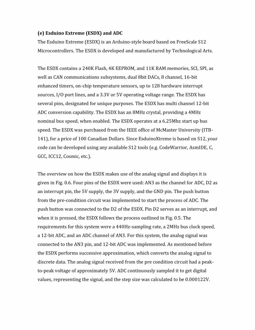
The graph for 50% of the Nyquist Rate of a sine waveform is presented in Fig. 1.
below.
Fig. 1.1: The output graph from Matlab at 50% of the Nyquist Rate of a sine waveform. The
graph can be seen to have sharp edges. The peak-to-peak voltage is still approximately 4.5V
The output graph from 50% of the Nyquist rate (110Hz), as seen in Fig. 1.1, can be
seen to have a rough shape. It is no longer smooth. Aliasing is evident from the
graph. At higher frequencies, it becomes increasingly difficult to obtain an accurate
graph.
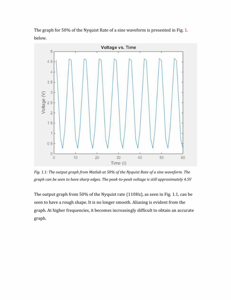
The output graph for 100% of the Nyquist Rate is shown below in Fig. 1.2 down
below
Fig. 1.1: The output graph from Matlab at 100% of the Nyquist Rate of a sine waveform. The
graph can be seen to have very sharp edges. The peak-to-peak voltage is still approximately
4.5V
As can be seen from Fig. 1.2 the graph is very sharp. It does not resemble a smooth
sine graph. Aliasing is very evident. The graph has come out incorrect and is difficult
to read.

5: Discussion
(1) Calculate the maximum quantization error.
The maximum quantization error can be calculated through the following
equation: VFS/(2m) where ‘m’ is the amount of bits in the ADC resolution.
Since the ADC resolution was 12 bits, ‘m’ equals 12.
Error=4/(2^12)
Error=0.0009765625
(2) Based upon your assigned bus speed, what is the maximum standard serial
communication rate you can implement?
The maximum serial communication rate you can apply depends upon the
bus speed as well as the Baud rate. The Baud rate is defined as the number of
signal changes the ESDX makes per second. For this project, a Baud rate of
9600 was chosen, however the maximum Baud rate that can be implemented
is 19200.
(3) Reviewing the entire system, which element is the primary limitation on
speed? How did you test this?
After many hours of debugging and thorough revision, the limiting factor was
determined to be the Baud rate.
(4) Based upon the Nyquist rate, what is the maximum frequency of the analog
signal you can effectively reproduce? What happens when your input signal
exceeds this frequency?
Depending on the Nyquist rate, sampling should occur at twice the frequency,
which is being used, at least. The project specifications required the sampling
frequency to be 440Hz; therefore the Nyquist rate was 220Hz. If the sample
frequency was greater than the Nyquist rate, a concept called Aliasing occurs.

Aliasing results in the digital signal obtained being invalid and flawed when
frequencies go above the limit, Nyquist rate.
(5) Are input signals with sharp transitions (e.g. square, saw-tooth, etc.)
accurately reproduced? Justify your answer
Input signals with sharp transitions were reproduced to an extent. At lower
frequencies, the output graphs were very accurate as is evident in Fig. 0.8.
However, at higher frequencies, these sharp transitions proved to be
detrimental to the output graph, as the graphs became increasingly
inaccurate with an increase in frequency. This can be explained by a lot of
factors. The baud rate selected was 9600; this might have been the factor as
to why the graph lost its smooth shape at higher frequencies. A different
baud rate, would have caused a smoother graph.

6: Conclusion
The purpose of this project was to construct a data acquisition system and
then display that output on any program. In order to accomplish this
purpose, the ESDX had to perform ADC and serially communicate with
MatLab. A pre-condition circuit was built to amplify the analog signal
received from the function generator.
The implications and uses of such a system range from simple to complex.
Physical phenomenon is usually in analog, like forces or temperature. A
computer does not work in analog; this is where this project comes into play.
It can convert physical quantities into a form the computer can understand
and work with. If a transducer is incorporated into this circuit, it can convert
signals from forces or temperature.
Such a system is fundamental for many other complex systems, such as
seismometers, which aid in earthquake detection, to oscilloscopes, which
display signals.

7: Appendix
CodeWarrior
#include <hidef.h> /* common defines and macros */
#include "derivative.h" /* derivative-specific definitions */
#include "SCI.h"
void SetClk(void); //initializing SetClk for bus speed
void delayby1ms(int k); //initializing delay function
//initializing values
char string[20];
unsigned short xval;
/////////////////////////////////////////////////////
void main(void) {
// Initialize uC environment//
SetClk(); //set bus speed to 8MHz
SCI_Init(9600);
// Configure on-board LED
DDRJ = 0x01; // Set pin D13 (on board LED) to an output
PTJ = 0x00; // Make sure the LED isn't on to begin with,
//SETTING ADC
ATDCTL1 = 0x4F; // 12-bit (ADC Resolution)

ATDCTL3 = 0x88; // right justified, one sample per sequence
ATDCTL4 = 0x02; // prescaler = 2; ATD clock = 6.25MHz / (2 * (2 + 1))
ATDCTL5 = 0x23; // Sets channel to AD3
DDRJ |= 0x01; // PortJ bit 0 is output to LED D2 on DIG13
/* ESDUINO PORT CONFIGURATION BELOW (Don't Edit) */
/////////////////////////////////////////////////////
/*
* The next six assignment statements configure the Timer Input Capture
*/
TSCR1 = 0x90; //Timer System Control Register 1
// TSCR1[7] = TEN: Timer Enable (0-disable, 1- enable)
// TSCR1[6] = TSWAI: Timer runs during WAI (0-enable, 1-disable)
// TSCR1[5] = TSFRZ: Timer runs during WAI (0- enable, 1-disable)
// TSCR1[4] = TFFCA: Timer Fast Flag Clear All (0-normal 1-read/write clears
interrupt flags)
// TSCR1[3] = PRT: Precision Timer (0-legacy, 1-precision)
// TSCR1[2:0] not used
TSCR2 = 0x01; //Timer System Control Register 2
// TSCR2[7] = TOI: Timer Overflow Interrupt Enable (0-inhibited, 1-hardware irq
when TOF=1)
// TSCR2[6:3] not used
// TSCR2[2:0] = Timer Prescaler Select: See Table22-12 of MC9S12G Family
Reference Manual r1.25 (set for bus/1)
TIOS = 0xFE; //Timer Input Capture or Output capture
//set TIC[0] and input (similar to DDR)
PERT = 0x01; //Enable Pull-Up resistor on TIC[0]
TCTL3 = 0x00; //TCTL3 & TCTL4 configure which edge(s) to capture
TCTL4 = 0x02; //Configured for falling edge on TIC[0]

/*
* The next one assignment statement configures the Timer Interrupt Enable
*/
TIE = 0x01; //Timer Interrupt Enable
/*
* The next one assignment statement configures the ESDX to catch
Interrupt Requests
*/
EnableInterrupts;
for(;;){
}
}
/* INTERRUPT SERIVE ROUTINES (ISRs) GO BELOW*/
/////////////////////////////////////////////////////
/* This is the Interrupt Service Routine for TIC channel 0 (Code
Warrior has predefined the name for you as "Vtimch0"
*/
interrupt VectorNumber_Vtimch0 void ISR_Vtimch0(void){
for(;;){
xval=ATDDR0; //set ADC channel
SCI_OutUDec(xval);
delayby1ms(2.27); // for 440Hz
SCI_OutChar(CR);
}
}
/////////////////////////////////////////////////////
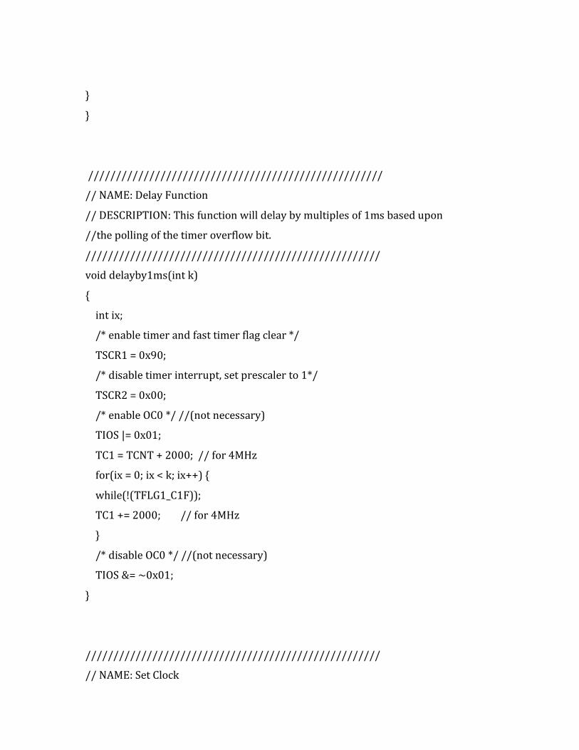
// NAME: Delay Function
// DESCRIPTION: This function will delay by multiples of 1ms based upon
//the polling of the timer overflow bit.
/////////////////////////////////////////////////////
void delayby1ms(int k)
{
int ix;
/* enable timer and fast timer flag clear */
TSCR1 = 0x90;
/* disable timer interrupt, set prescaler to 1*/
TSCR2 = 0x00;
/* enable OC0 */ //(not necessary)
TIOS |= 0x01;
TC1 = TCNT + 2000; // for 4MHz
for(ix = 0; ix < k; ix++) {
while(!(TFLG1_C1F));
TC1 += 2000; // for 4MHz
}
/* disable OC0 */ //(not necessary)
TIOS &= ~0x01;
}
/////////////////////////////////////////////////////
// NAME: Set Clock

// DESCRIPTION: The following code is adapted from the ESDX User Guide
//and the Serial Monitor code (S12SerMon2r7) to set the clock speed.
// We will discuss this section in-depth in lecture
// NOTE: CLOCK IS ALREADY INCLUDED IN THE MAIN LOOP DO NOT EDIT
/////////////////////////////////////////////////////
void SetClk(void){
//fbus = 4MHz
CPMUPROT = 0x26; //we were told to put this in
CPMUCLKS = 0x80; //PLL = 1
CPMUOSC = 0x00; //OSCE = 0 Internal Oscillator is selected
CPMUSYNR = 0x07; //VCOFRQ=16 MHz and SYNDIV = 7
//now fREF = 1MHz and fVCO = 2*fref*(7+1) = 16
CPMUFLG = 0x00;
}
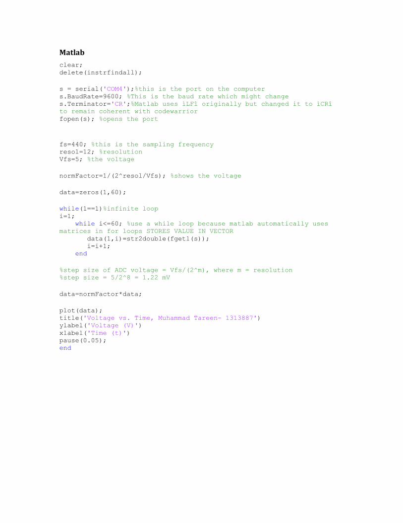
Matlab
clear; delete(instrfindall);
s = serial('COM4');%this is the port on the computer s.BaudRate=9600; %This is the baud rate which might change s.Terminator='CR';%Matlab uses ìLFî originally but changed it to ìCRî
to remain coherent with codewarrior fopen(s); %opens the port
fs=440; %this is the sampling frequency resol=12; %resolution Vfs=5; %the voltage
normFactor=1/(2^resol/Vfs); %shows the voltage
data=zeros(1,60);
while(1==1)%infinite loop i=1; while i<=60; %use a while loop because matlab automatically uses
matrices in for loops STORES VALUE IN VECTOR data(1,i)=str2double(fgetl(s)); i=i+1; end
%step size of ADC voltage = Vfs/(2^m), where m = resolution %step size = 5/2^8 = 1.22 mV
data=normFactor*data;
plot(data); title('Voltage vs. Time, Muhammad Tareen- 1313887') ylabel('Voltage (V)') xlabel('Time (t)') pause(0.05); end