Embed Size (px)
Citation preview
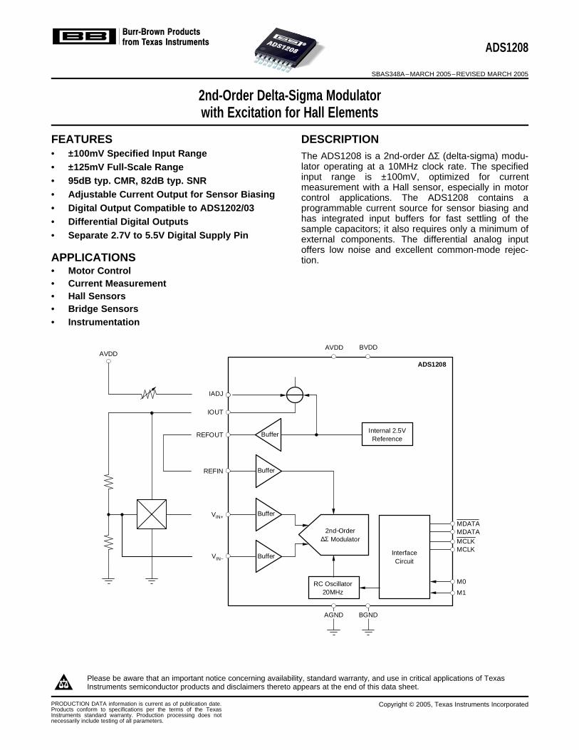
FEATURES DESCRIPTION
APPLICATIONS
Internal 2.5VReference
RC Oscillator20MHz
InterfaceCircuit
MDATA
IADJ
IOUT
AVDD
ADS1208
REFOUT
REFIN
VIN+
VIN−
MDATA
BVDD
MCLK
M0
M1
MCLK
Buffer
Buffer
Buffer
Buffer
2nd−Order∆Σ Modulator
BGNDAGND
AVDD
ADS1208
SBAS348A–MARCH 2005–REVISED MARCH 2005
2nd-Order Delta-Sigma Modulatorwith Excitation for Hall Elements
• ±100mV Specified Input Range The ADS1208 is a 2nd-order ∆Σ (delta-sigma) modu-lator operating at a 10MHz clock rate. The specified• ±125mV Full-Scale Rangeinput range is ±100mV, optimized for current• 95dB typ. CMR, 82dB typ. SNRmeasurement with a Hall sensor, especially in motor
• Adjustable Current Output for Sensor Biasing control applications. The ADS1208 contains a• Digital Output Compatible to ADS1202/03 programmable current source for sensor biasing and
has integrated input buffers for fast settling of the• Differential Digital Outputssample capacitors; it also requires only a minimum of
• Separate 2.7V to 5.5V Digital Supply Pin external components. The differential analog inputoffers low noise and excellent common-mode rejec-tion.
• Motor Control• Current Measurement• Hall Sensors• Bridge Sensors• Instrumentation
Please be aware that an important notice concerning availability, standard warranty, and use in critical applications of TexasInstruments semiconductor products and disclaimers thereto appears at the end of this data sheet.
PRODUCTION DATA information is current as of publication date. Copyright © 2005, Texas Instruments IncorporatedProducts conform to specifications per the terms of the TexasInstruments standard warranty. Production processing does notnecessarily include testing of all parameters.
www.ti.com
Package/Ordering Information
ABSOLUTE MAXIMUM RATINGS
RECOMMENDED OPERATING CONDITIONS
DISSIPATION RATINGS TABLE
ADS1208
SBAS348A–MARCH 2005–REVISED MARCH 2005
This integrated circuit can be damaged by ESD. Texas Instruments recommends that all integratedcircuits be handled with appropriate precautions. Failure to observe proper handling and installationprocedures can cause damage.
ESD damage can range from subtle performance degradation to complete device failure. Precisionintegrated circuits may be more susceptible to damage because very small parametric changes couldcause the device not to meet its published specifications.
For the most current package and ordering information, see the Package Option Addendum at the end of thisdocument, or see the TI web site at www.ti.com.
over operating free-air temperature range (unless otherwise noted) (1)
ADS1208I UNIT
Supply voltage, AGND to AVDD –0.3 to +6 V
Supply voltage, BGND to BVDD –0.3 to +6 V
Analog input voltage with respect to AGND AGND – 0.3 to AVDD + 0.3 V
Reference input voltage with respect to AGND AGND – 0.3 to AVDD + 0.3 V
Digital input voltage with respect to BGND BGND – 0.3 to BVDD + 0.3 V
Ground voltage difference AGND to BGND ±0.3 V
Input current to any pin except supply ±10 mA
Power dissipation See Dissipation Ratings Table
Operating virtual junction temperature range, TJ –40 to +150 °C
Operating free-air temperature range, TA –40 to +85 °C
Storage temperature range, TSTG –65 to +150 °C
(1) Stresses beyond those listed under Absolute Maximum Ratings may cause permanent damage to the device. These are stress ratingsonly, and functional operation of the device at these or any other conditions beyond those indicated under Recommended OperatingConditions is not implied. Exposure to absolute-maximum-rated conditions for extended periods may affect device reliability.
PARAMETER MIN NOM MAX UNIT
Supply voltage, AGND to AVDD 4.5 5.0 5.5 V
Low-voltage levels 2.7 3.6 VSupply voltage, BGND to BVDD
5V logic levels 4.5 5.0 5.5 V
Reference input voltage 0.5 2.5 3.0 V
Analog inputs VIN+– VIN- –VREFIN /20 +VREFIN /20 V
DERATING FACTOR TA≤ 25°C TA = 70°C TA = 85°CBOARD PACKAGE RθJC RθJA ABOVE TA = 25°C POWER RATING POWER RATING POWER RATING
Low-K (1) PW 35°C/W 147°C/W 6.8mW/°C 850mW 544mW 442mW
High-K (2) PW 33.6°C/W 108.4°C 9.225W/°C 1150mW 738mW 600mW
(1) The JEDEC low-K (1s) board used to derive this data was a 3in x 3in, two-layer board with 2-ounce copper traces on top of the board.(2) The JEDEC high-K (2s2p) board used to derive this data was a 3in x 3in, multilayer board with 1-ounce internal power and ground
planes and 2-ounce copper traces on top and bottom of the board.
2
www.ti.com
ELECTRICAL CHARACTERISTICS
ADS1208
SBAS348A–MARCH 2005–REVISED MARCH 2005
Over recommended operating free-air temperature range at –40°C to +85°C, AVDD = BVDD = +5V, VREF = internal +2.5V,Mode 3, MCLK input = 20MHz, differential input voltage = 200mVPP, common-mode voltage = 1.4V, and 16-bit Sinc3 filter withOSR = 256, unless otherwise noted.
ADS1208I
PARAMETER TEST CONDITIONS MIN TYP (1) MAX UNIT
Resolution 16 Bits
DC Accuracy
Integral nonlinearity (2) 16-bit resolution –8 1.6 8 LSB
Integral nonlinearity –0.012 0.0025 0.012 %
Differential nonlinearity (3) 16-bit resolution –1.0 1.0 LSB
Input offset (4) –2.0 –1.4 0 mV
Input offset drift 2.0 8.0 µV/°C
Gain error (4) Referenced to voltage at REFIN –1.25 –0.7 1.25 %
Gain error drift Referenced to voltage at REFIN 15 ppm/°C
Power-supply rejection ratio 66 dB
Analog Input
Full-scale range VIN+– VIN– –125 125 mV
Operating common-mode signal 0.8 1.4 2.5 V
Input capacitance 5.0 pF
Common-mode rejection 95 dB
Current Source (IOUT)
Output current (5) IOUT 1.0 5.0 8.0 mA
Voltage at IOUT pin VOUT 0 AVDD – 1.0 V
Voltage between AVDD pin and IADJ VADJ at IOUT = 1mA to 8mA 480 500 520 mV
Internal Voltage Reference
Reference output voltage REFOUT 2.45 2.5 2.55 V
Reference temperature drift 20 ppm/°C
Output resistance 0.3 Ω
Output source current 3.0 mA
Power-supply rejection ratio 60 dB
Startup time 0.1 ms
Voltage Reference Input
Reference voltage input REFIN 0.5 3.0 V
Reference input capacitance 5 pF
Reference input current -50 +50 nA
Internal Clock for Modes 0, 1 and 2
Clock frequency 8.0 10.1 12.0 MHz
External Clock for Mode 3
Clock frequency 1.0 24.0 MHz
(1) All values are at TA = 25°C.(2) Integral nonlinearity is defined as the maximum deviation of the line through the end points of the specified input range of the transfer
curve for VIN+– VIN– = –100mV to +100mV, expressed either as the number of LSBs or as a percent of the measured input range(200mV).
(3) Ensured by design.(4) Maximum values, including temperature drift, are ensured over the full specified temperature range.(5) It is possible to leave pin IOUT unconnected (IOUT = 0mA).
3
www.ti.com
ADS1208
SBAS348A–MARCH 2005–REVISED MARCH 2005
ELECTRICAL CHARACTERISTICS (continued)
Over recommended operating free-air temperature range at –40°C to +85°C, AVDD = BVDD = +5V, VREF = internal +2.5V,Mode 3, MCLK input = 20MHz, differential input voltage = 200mVPP, common-mode voltage = 1.4V, and 16-bit Sinc3 filter withOSR = 256, unless otherwise noted.
ADS1208I
PARAMETER TEST CONDITIONS MIN TYP (1) MAX UNIT
AC Accuracy
SNR VIN = 200mVPP at 1kHz 80 82 dB
SINAD VIN = 200mVPP at 1kHz 77 81.5 dB
THD VIN = 200mVPP at 1kHz –91 –80 dB
SFDR VIN = 200mVPP at 1kHz 80 93 dB
Digital Inputs (6)
Logic family CMOS
VIH High-level input voltage 0.7 x BVDD BVDD + 0.3 V
VIL Low-level input voltage –0.3 0.3 x BVDD V
IIN Input current VIN = BVDD or GND –50 50 nA
CI Input capacitance 5 pF
Digital Outputs (6)
Logic family CMOS
VOH High-level output voltage BVDD = 4.5V, IOH = –100µA 4.44 V
VOL Low-level output voltage BVDD = 4.5V, IOL = +100µA 0.5 V
CL Load capacitance 30 pF
Data format Bit stream
Digital Inputs (7)
Logic family LVCMOS
VIH High-level input voltage BVDD = 3.6V 2 BVDD + 0.3 V
VIL Low-level input voltage BVDD = 2.7V –0.3 0.8 V
IIN Input current VIN = BVDD or GND –50 50 nA
CI Input capacitance 5 pF
Digital Outputs (7)
Logic family LVCMOS
VOH High-level output voltage BVDD = 2.7, IOH = –100µA BVDD – 0.2 V
VOL Low-level output voltage BVDD = 2.7, IOL = +100µA 0.2 V
CL Load capacitance 30 pF
Data format Bit stream
Power Supply
Analog supply voltage, AVDD 4.5 5.0 5.5 V
Digital interface supply voltage, BVDD 2.7 5 5.5 V
Operating supply current, AIDD Modes 0, 1 and 2 11.9 15.0 mA
Operating supply current, AIDD Mode 3 11.5 14.5 mA
Operating supply current, BIDD Modes 0, 1 and 2 2.3 3.0 mA
Operating supply current, BIDD Mode 3 1.3 2.0 mA
Power dissipation Modes 0, 1 and 2 71 90 mW
Power dissipation Mode 3 64 82.5 mW
(6) Applicable for 5.0V nominal supply; BVDD (min) = 4.5V and BVDD (max) = 5.5V.(7) Applicable for 3.0V nominal supply; BVDD (min) = 2.7V and BVDD (max) = 3.6V
4
www.ti.com
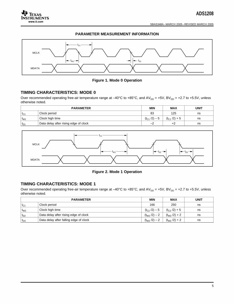
MCLK
MDATA
tC1
tW1 tD1
TIMING CHARACTERISTICS: MODE 0
MCLK
MDATA
tC2
tW2 tD2 tD3
TIMING CHARACTERISTICS: MODE 1
ADS1208
SBAS348A–MARCH 2005–REVISED MARCH 2005
PARAMETER MEASUREMENT INFORMATION
Figure 1. Mode 0 Operation
Over recommended operating free-air temperature range at –40°C to +85°C, and AVDD = +5V, BVDD = +2.7 to +5.5V, unlessotherwise noted.
PARAMETER MIN MAX UNIT
tC1 Clock period 83 125 ns
tW1 Clock high time (tC1 /2) – 5 (tC1 /2) + 5 ns
tD1 Data delay after rising edge of clock –2 +2 ns
Figure 2. Mode 1 Operation
Over recommended operating free-air temperature range at –40°C to +85°C, and AVDD = +5V, BVDD = +2.7 to +5.5V, unlessotherwise noted.
PARAMETER MIN MAX UNIT
tC1 Clock period 166 250 ns
tW2 Clock high time (tC2 /2) – 5 (tC2 /2) + 5 ns
tD2 Data delay after rising edge of clock (tW2 /2) – 2 (tW2 /2) + 2 ns
tD3 Data delay after falling edge of clock (tW2 /2) – 2 (tW2 /2) + 2 ns
5
www.ti.com
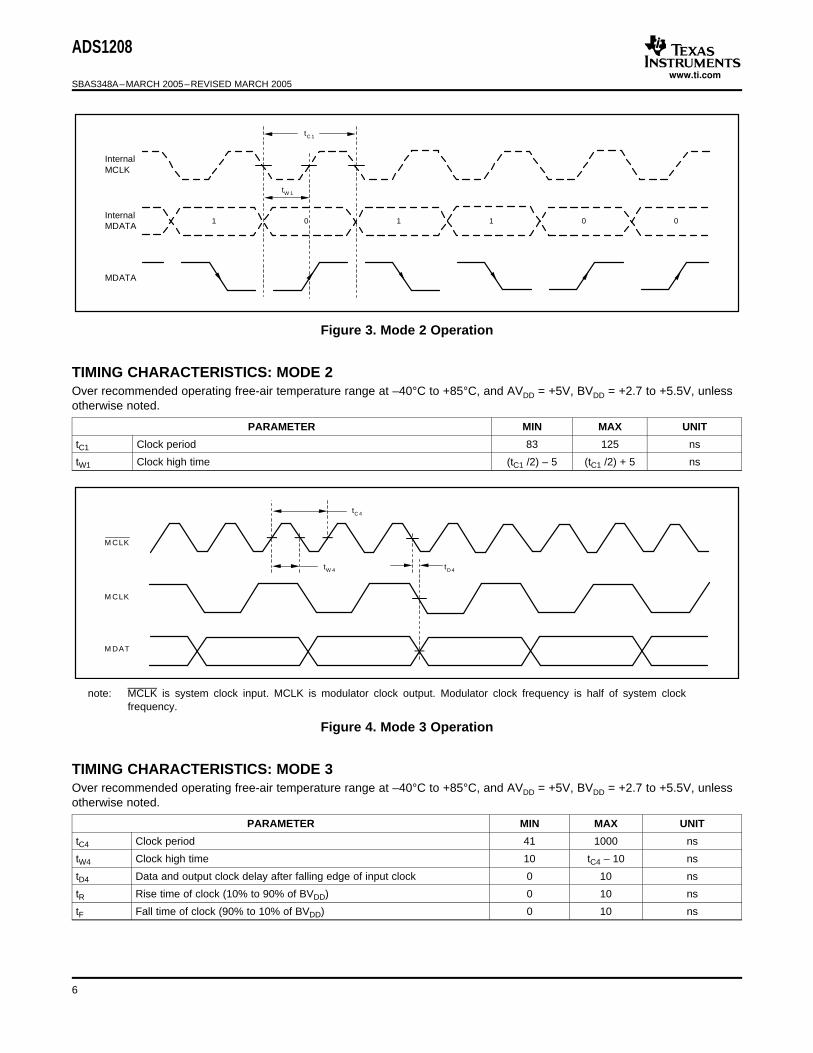
InternalMCLK
InternalMDATA
MDATA
tC 1
tW 1
1 0 1 1 0 0
TIMING CHARACTERISTICS: MODE 2
M DAT
M CLK
tC 4
tW 4 tD 4
M CLK
TIMING CHARACTERISTICS: MODE 3
ADS1208
SBAS348A–MARCH 2005–REVISED MARCH 2005
Figure 3. Mode 2 Operation
Over recommended operating free-air temperature range at –40°C to +85°C, and AVDD = +5V, BVDD = +2.7 to +5.5V, unlessotherwise noted.
PARAMETER MIN MAX UNIT
tC1 Clock period 83 125 ns
tW1 Clock high time (tC1 /2) – 5 (tC1 /2) + 5 ns
note: MCLK is system clock input. MCLK is modulator clock output. Modulator clock frequency is half of system clockfrequency.
Figure 4. Mode 3 Operation
Over recommended operating free-air temperature range at –40°C to +85°C, and AVDD = +5V, BVDD = +2.7 to +5.5V, unlessotherwise noted.
PARAMETER MIN MAX UNIT
tC4 Clock period 41 1000 ns
tW4 Clock high time 10 tC4 – 10 ns
tD4 Data and output clock delay after falling edge of input clock 0 10 ns
tR Rise time of clock (10% to 90% of BVDD) 0 10 ns
tF Fall time of clock (90% to 10% of BVDD) 0 10 ns
6
www.ti.com
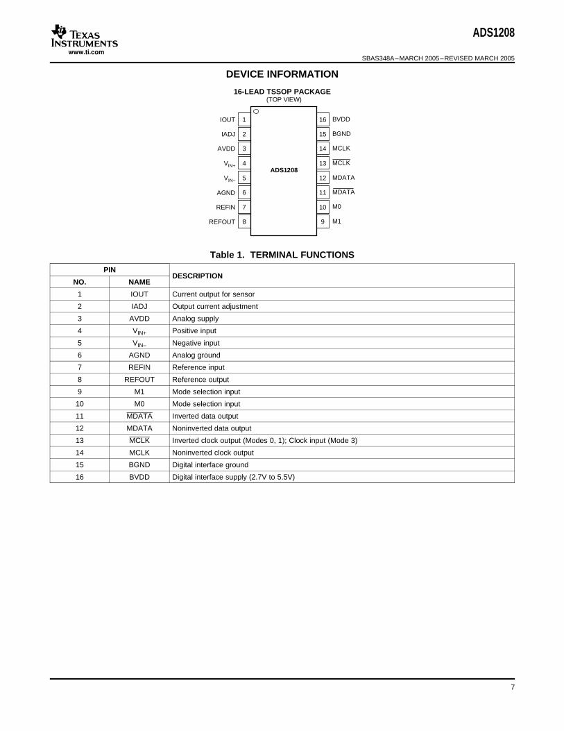
DEVICE INFORMATION
1
2
3
4
16
15
14
13
BVDD
BGND
MCLK
MCLK
12
11
10
9
MDATA
MDATA
M0
M1
ADS1208
(TOP VIEW)
IOUT
IADJ
AVDD
VIN+
VIN−
AGND
REFIN
REFOUT
5
6
7
8
ADS1208
SBAS348A–MARCH 2005–REVISED MARCH 2005
16-LEAD TSSOP PACKAGE
Table 1. TERMINAL FUNCTIONS
PINDESCRIPTION
NO. NAME
1 IOUT Current output for sensor
2 IADJ Output current adjustment
3 AVDD Analog supply
4 VIN+ Positive input
5 VIN– Negative input
6 AGND Analog ground
7 REFIN Reference input
8 REFOUT Reference output
9 M1 Mode selection input
10 M0 Mode selection input
11 MDATA Inverted data output
12 MDATA Noninverted data output
13 MCLK Inverted clock output (Modes 0, 1); Clock input (Mode 3)
14 MCLK Noninverted clock output
15 BGND Digital interface ground
16 BVDD Digital interface supply (2.7V to 5.5V)
7
www.ti.com
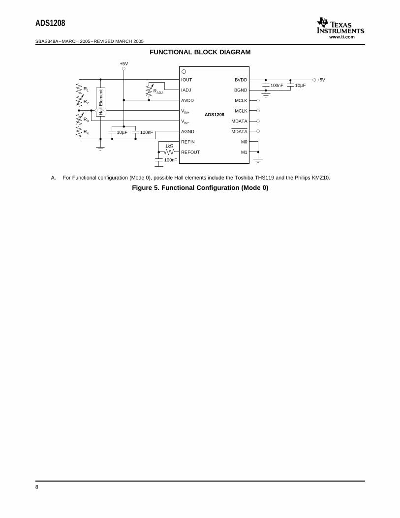
ADS1208
IOUT
IADJ
AVDD
VIN+
VIN−
AGND
REFIN
REFOUT
BVDD
BGND
MCLK
MCLK
MDATA
MDATA
M0
M11kΩ
100nF 10µF
R2
R1
R4
R3
RADJ
100nF
10µF 100nF
Hal
lEle
me
nt
+5V
+5V
ADS1208
SBAS348A–MARCH 2005–REVISED MARCH 2005
FUNCTIONAL BLOCK DIAGRAM
A. For Functional configuration (Mode 0), possible Hall elements include the Toshiba THS119 and the Philips KMZ10.
Figure 5. Functional Configuration (Mode 0)
8
www.ti.com
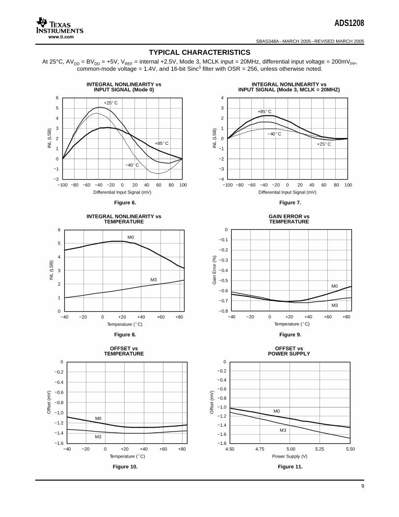
TYPICAL CHARACTERISTICS
Differential Input Signal (mV)
INL
(LS
B)
0−100 100−80 80−60 60−40 40−20 20
6
5
4
3
2
1
0
−1
−2
+25C
−40C
+85C
Differential Input Signal (mV)
INL
(LS
B)
0−100 100−80 80−60 60−40 40−20 20
4
3
2
1
0
−1
−2
−3
−4
+25C
−40C
+85C
Temperature (C)
INL
(LS
B)
0−40 +80+60+40−20 +20
6
5
4
3
2
1
0
M0
M3
Temperature (C)
Gai
nE
rror
(%)
0−40 +80+60+40−20 +20
0
−0.1
−0.2
−0.3
−0.4
−0.5
−0.6
−0.7
−0.8
M0
M3
Temperature (C)
Offs
et(m
V)
0−40 +80+60+40−20 +20
0
−0.2
−0.4
−0.6
−0.8
−1.0
−1.2
−1.4
−1.6
M0
M3
Power Supply (V)
Offs
et(m
V)
4.50 4.75 5.00 5.25 5.50
0
−0.2
−0.4
−0.6
−0.8
−1.0
−1.2
−1.4
−1.6
−1.8
M0
M3
ADS1208
SBAS348A–MARCH 2005–REVISED MARCH 2005
At 25°C, AVDD = BVDD = +5V, VREF = internal +2.5V, Mode 3, MCLK input = 20MHz, differential input voltage = 200mVPP,common-mode voltage = 1.4V, and 16-bit Sinc3 filter with OSR = 256, unless otherwise noted.
INTEGRAL NONLINEARITY vs INTEGRAL NONLINEARITY vsINPUT SIGNAL (Mode 0) INPUT SIGNAL (Mode 3, MCLK = 20MHZ)
Figure 6. Figure 7.
INTEGRAL NONLINEARITY vs GAIN ERROR vsTEMPERATURE TEMPERATURE
Figure 8. Figure 9.
OFFSET vs OFFSET vsTEMPERATURE POWER SUPPLY
Figure 10. Figure 11.
9
www.ti.com
Temperature (C)
SN
R(d
B)
0−40 +80+60+40−20 +20
85
84
83
82
81
80
79
78
M0
M3
Temperature (C)
SIN
AD
(dB
)
0−40 +80+60+40−20 +20
85
84
83
82
81
80
79
78
M0
M3
Decimation Ratio (OSR)
EN
OB
(BIts
)
1 10 100 1000
16
14
12
10
8
6
4
2
0
Sinc1
Sinc2
Sinc3
Sincfast
Decimation Ratio (OSR)
SN
R(d
B)
1 10 100 1000
100
90
80
70
60
50
40
30
20
10
0
Sinc2Sinc3
ADS1208
SBAS348A–MARCH 2005–REVISED MARCH 2005
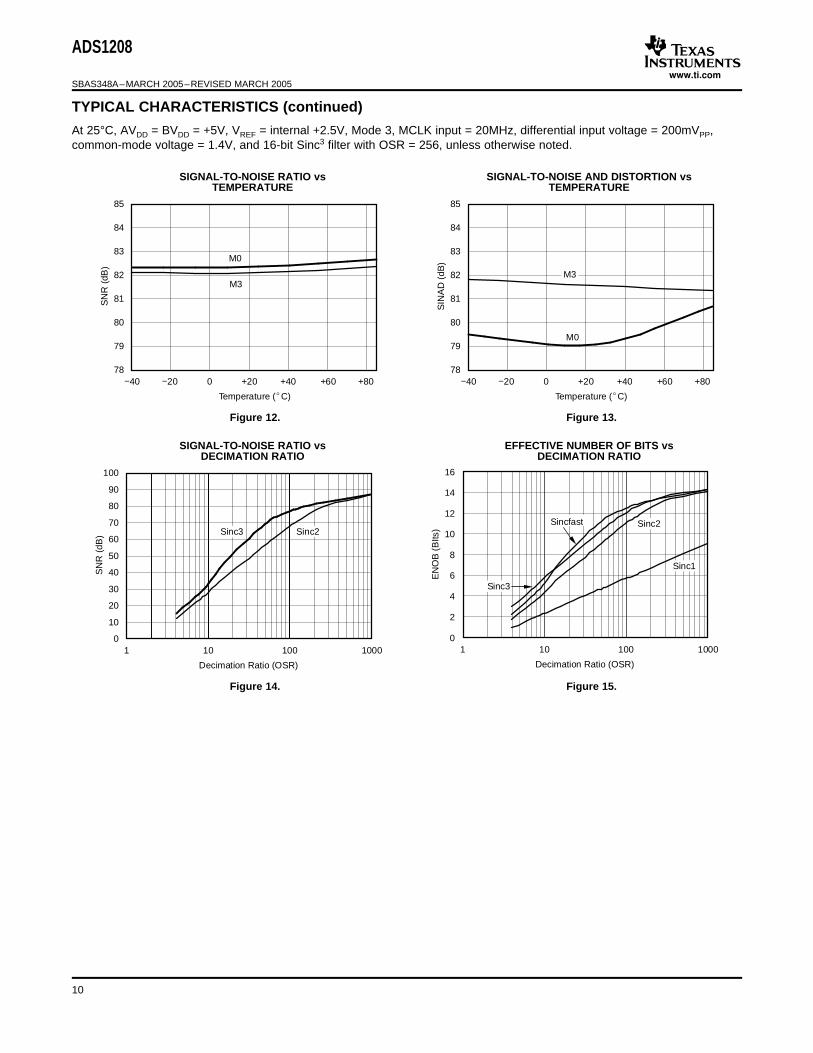
TYPICAL CHARACTERISTICS (continued)
At 25°C, AVDD = BVDD = +5V, VREF = internal +2.5V, Mode 3, MCLK input = 20MHz, differential input voltage = 200mVPP,common-mode voltage = 1.4V, and 16-bit Sinc3 filter with OSR = 256, unless otherwise noted.
SIGNAL-TO-NOISE RATIO vs SIGNAL-TO-NOISE AND DISTORTION vsTEMPERATURE TEMPERATURE
Figure 12. Figure 13.
SIGNAL-TO-NOISE RATIO vs EFFECTIVE NUMBER OF BITS vsDECIMATION RATIO DECIMATION RATIO
Figure 14. Figure 15.
10
www.ti.com
Temperature (C)S
FD
R(d
B)
0−40 +80+60+40−20 +20
105
100
95
90
85
80
SFDR
THD
−105
−100
−95
−90
−85
−80
TH
D(d
B)
Temperature (C)
SF
DR
(dB
)
0−40 +80+60+40−20 +20
105
100
95
90
85
80
SFDR
THD
−105
−100
−95
−90
−85
−80
TH
D(d
B)
fSIG (kHz)
SF
DR
(dB
)
0 5 1510 20
105
100
95
90
85
80
SFDR
THD
−105
−100
−95
−90
−85
−80
TH
D(d
B)
fSIG (kHz)
SF
DR
(dB
)
0 5 1510 20
105
100
95
90
85
80
SFDR
THD
−105
−100
−95
−90
−85
−80
TH
D(d
B)
ADS1208
SBAS348A–MARCH 2005–REVISED MARCH 2005
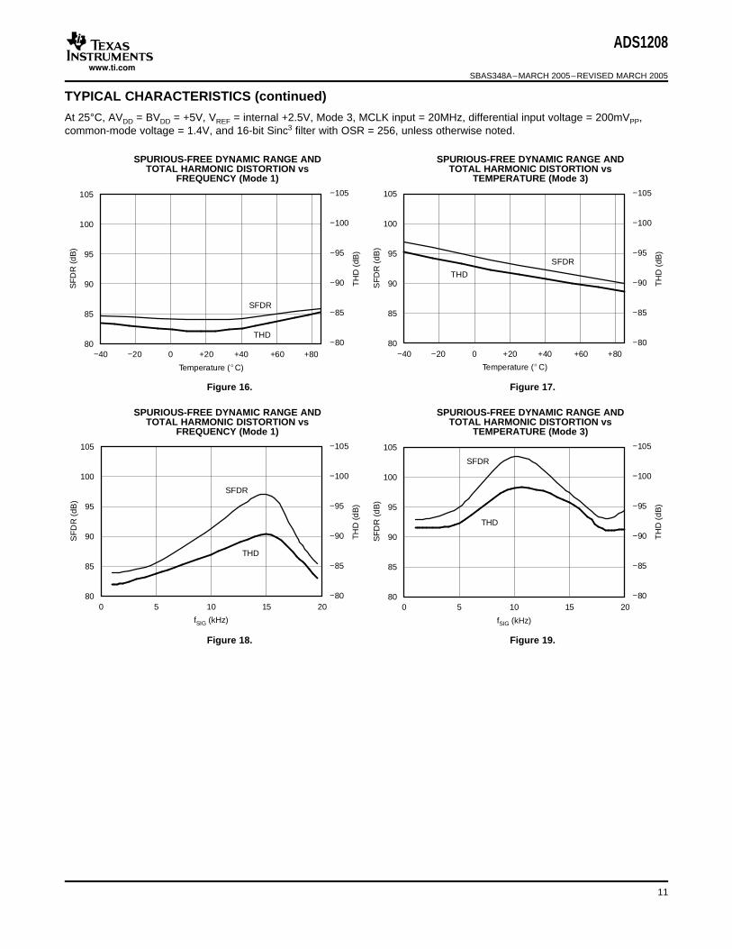
TYPICAL CHARACTERISTICS (continued)
At 25°C, AVDD = BVDD = +5V, VREF = internal +2.5V, Mode 3, MCLK input = 20MHz, differential input voltage = 200mVPP,common-mode voltage = 1.4V, and 16-bit Sinc3 filter with OSR = 256, unless otherwise noted.
SPURIOUS-FREE DYNAMIC RANGE AND SPURIOUS-FREE DYNAMIC RANGE ANDTOTAL HARMONIC DISTORTION vs TOTAL HARMONIC DISTORTION vs
FREQUENCY (Mode 1) TEMPERATURE (Mode 3)
Figure 16. Figure 17.
SPURIOUS-FREE DYNAMIC RANGE AND SPURIOUS-FREE DYNAMIC RANGE ANDTOTAL HARMONIC DISTORTION vs TOTAL HARMONIC DISTORTION vs
FREQUENCY (Mode 1) TEMPERATURE (Mode 3)
Figure 18. Figure 19.
11
www.ti.com
Frequency (kHz)
Ma
gnitu
de(d
B)
0 5 1510 20
0
−20
−40
−60
−80
−100
−120
−140
Frequency (kHz)
Ma
gnitu
de(d
B)
0 5 1510 20
0
−20
−40
−60
−80
−100
−120
−140
Frequency (kHz)
CM
RR
(dB
)
1 10 100 1000
110
105
100
95
90
85
80
75
70
65
60
M0
M3
Frequency (kHz)
PS
RR
(dB
)
0.1 1 10 100 1000
90
85
80
75
70
65
60
55
50
M0
M3
Temperature (C)
MC
LK
(MH
z)
0−40 +80+60+40−20 +20
10.6
10.5
10.4
10.3
10.2
10.1
10.0
9.9
9.8
9.7
9.6
VDD (V)
MC
LK
(MH
z)
4.50 4.75 5.255.00 5.50
10.20
10.15
10.10
10.05
10.00
9.95
ADS1208
SBAS348A–MARCH 2005–REVISED MARCH 2005
TYPICAL CHARACTERISTICS (continued)
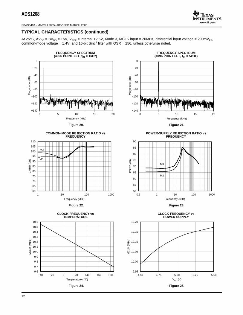
At 25°C, AVDD = BVDD = +5V, VREF = internal +2.5V, Mode 3, MCLK input = 20MHz, differential input voltage = 200mVPP,common-mode voltage = 1.4V, and 16-bit Sinc3 filter with OSR = 256, unless otherwise noted.
FREQUENCY SPECTRUM FREQUENCY SPECTRUM(4096 POINT FFT, fIN = 1kHz) (4096 POINT FFT, fIN = 5kHz)
Figure 20. Figure 21.
COMMON-MODE REJECTION RATIO vs POWER-SUPPLY REJECTION RATIO vsFREQUENCY FREQUENCY
Figure 22. Figure 23.
CLOCK FREQUENCY vs CLOCK FREQUENCY vsTEMPERATURE POWER SUPPLY
Figure 24. Figure 25.
12
www.ti.com
Temperature (C)
I DD
(mA
)
0−40 +80+60+40−20 +20
14
13
12
11
10
9
8
M0
M3
Temperature (C)
I DD
(mA
)
0−40 +80+60+40−20 +20
3.0
2.5
2.0
1.5
1.0
0.5
0
M0
M3
Temperature (C)
VR
EF
(V)
0−40 +80+60+40−20 +20
2.5000
2.4998
2.4996
2.4994
2.4992
2.4990
2.4988
2.4986
2.4984
2.4982
2.4980
VDD (V)
VR
EF
(V)
3.0 4.03.5 5.04.5 5.5 6.0
2.5000
2.4998
2.4996
2.4994
2.4992
2.4990
2.4988
2.4986
2.4984
2.4982
2.4980
IOUT (mA)
VR
EF
(V)
−5 50 1510 20
2.525
2.520
2.515
2.510
2.505
2.500
2.495
2.490
2.485
2.480
2.475
5.5V
5.0V
4.5V
VOUT (V)
VR
EF
(mV
)
0 21 43 65
499.2
499.1
499.0
498.9
498.8
498.7
498.6
498.5
498.4
498.3
498.2
VDD = 5.0V
VDD = 4.5V
VDD = 5.5V
ADS1208
SBAS348A–MARCH 2005–REVISED MARCH 2005
TYPICAL CHARACTERISTICS (continued)
At 25°C, AVDD = BVDD = +5V, VREF = internal +2.5V, Mode 3, MCLK input = 20MHz, differential input voltage = 200mVPP,common-mode voltage = 1.4V, and 16-bit Sinc3 filter with OSR = 256, unless otherwise noted.
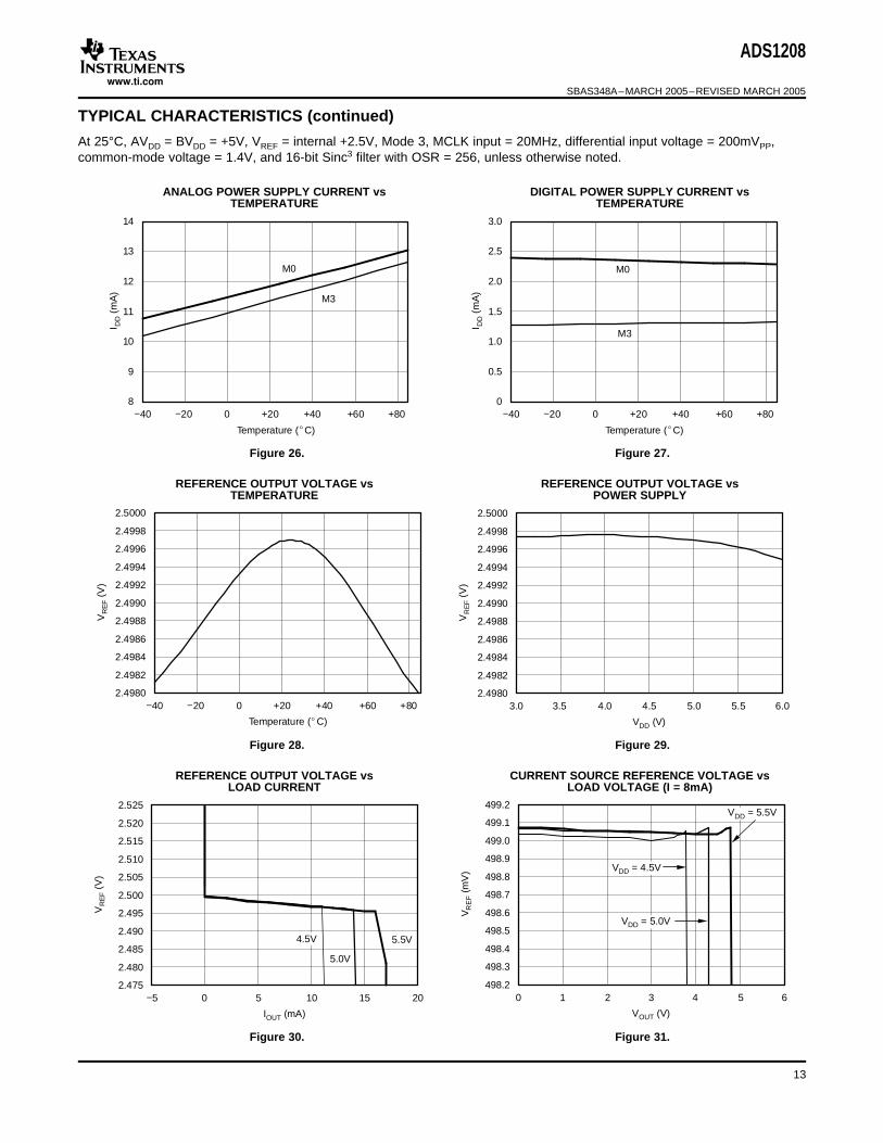
ANALOG POWER SUPPLY CURRENT vs DIGITAL POWER SUPPLY CURRENT vsTEMPERATURE TEMPERATURE
Figure 26. Figure 27.
REFERENCE OUTPUT VOLTAGE vs REFERENCE OUTPUT VOLTAGE vsTEMPERATURE POWER SUPPLY
Figure 28. Figure 29.
REFERENCE OUTPUT VOLTAGE vs CURRENT SOURCE REFERENCE VOLTAGE vsLOAD CURRENT LOAD VOLTAGE (I = 8mA)
Figure 30. Figure 31.
13
www.ti.com
Temperature (C)
VA
DJ
(mV
)
0−40 +80+60+40−20 +20
499.2
499.1
499.0
498.9
498.8
498.7
498.6
498.5
498.4
498.3
498.2
VDD (V)
VA
DJ
(mV
)
4.00 5.254.25 5.004.50 5.50 6.005.754.75
499.2
499.1
499.0
498.9
498.8
498.7
498.6
498.5
498.4
498.3
498.2
Differential Input Voltage (V)
RM
SN
ois
e(µ
V)
−125 −100 −75 −50 −25 1250 25 7550 100
10
9
8
7
6
5
4
3
2
1
0
ADS1208
SBAS348A–MARCH 2005–REVISED MARCH 2005
TYPICAL CHARACTERISTICS (continued)
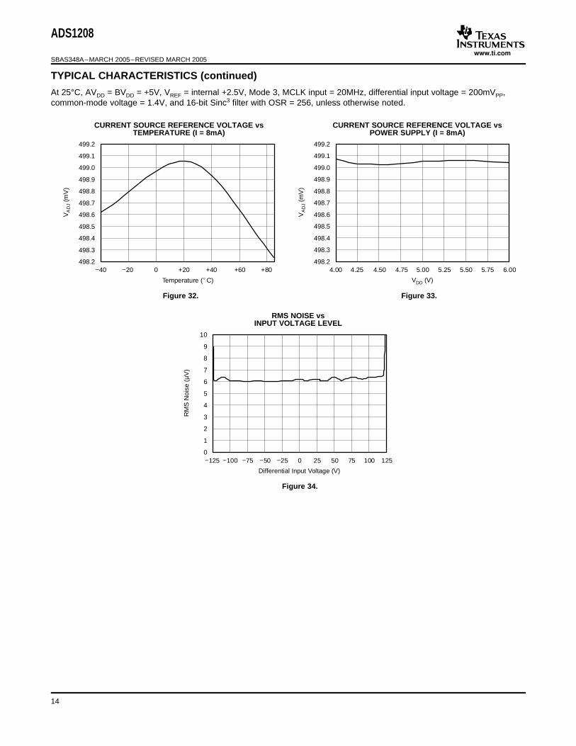
At 25°C, AVDD = BVDD = +5V, VREF = internal +2.5V, Mode 3, MCLK input = 20MHz, differential input voltage = 200mVPP,common-mode voltage = 1.4V, and 16-bit Sinc3 filter with OSR = 256, unless otherwise noted.
CURRENT SOURCE REFERENCE VOLTAGE vs CURRENT SOURCE REFERENCE VOLTAGE vsTEMPERATURE (I = 8mA) POWER SUPPLY (I = 8mA)
Figure 32. Figure 33.
RMS NOISE vsINPUT VOLTAGE LEVEL
Figure 34.
14
www.ti.com
APPLICATION INFORMATION
GENERAL DESCRIPTION
Analog Inputs
Delta−SigmaModulator
AZ
AVDD
VIN+
VIN−
AZ
ANALOG SECTION
Modulator
ADS1208
SBAS348A–MARCH 2005–REVISED MARCH 2005
should be used at the output of the delta-sigmamodulator. The primary purpose of the digital filter isto remove high-frequency noise. The secondary pur-
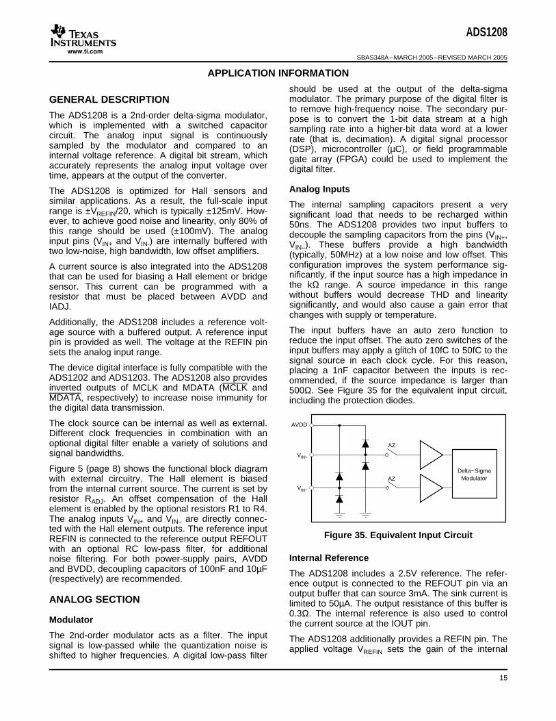
The ADS1208 is a 2nd-order delta-sigma modulator, pose is to convert the 1-bit data stream at a highwhich is implemented with a switched capacitor sampling rate into a higher-bit data word at a lowercircuit. The analog input signal is continuously rate (that is, decimation). A digital signal processorsampled by the modulator and compared to an (DSP), microcontroller (µC), or field programmableinternal voltage reference. A digital bit stream, which gate array (FPGA) could be used to implement theaccurately represents the analog input voltage over digital filter.time, appears at the output of the converter.
The ADS1208 is optimized for Hall sensors andsimilar applications. As a result, the full-scale input The internal sampling capacitors present a veryrange is ±VREFIN/20, which is typically ±125mV. How- significant load that needs to be recharged withinever, to achieve good noise and linearity, only 80% of 50ns. The ADS1208 provides two input buffers tothis range should be used (±100mV). The analog decouple the sampling capacitors from the pins (VIN+,input pins (VIN+ and VIN-) are internally buffered with VIN–). These buffers provide a high bandwidthtwo low-noise, high bandwidth, low offset amplifiers. (typically, 50MHz) at a low noise and low offset. This
configuration improves the system performance sig-A current source is also integrated into the ADS1208nificantly, if the input source has a high impedance inthat can be used for biasing a Hall element or bridgethe kΩ range. A source impedance in this rangesensor. This current can be programmed with awithout buffers would decrease THD and linearityresistor that must be placed between AVDD andsignificantly, and would also cause a gain error thatIADJ.changes with supply or temperature.
Additionally, the ADS1208 includes a reference volt-The input buffers have an auto zero function toage source with a buffered output. A reference inputreduce the input offset. The auto zero switches of thepin is provided as well. The voltage at the REFIN pininput buffers may apply a glitch of 10fC to 50fC to thesets the analog input range.signal source in each clock cycle. For this reason,
The device digital interface is fully compatible with the placing a 1nF capacitor between the inputs is rec-ADS1202 and ADS1203. The ADS1208 also provides ommended, if the source impedance is larger thaninverted outputs of MCLK and MDATA (MCLK and 500Ω. See Figure 35 for the equivalent input circuit,MDATA, respectively) to increase noise immunity for including the protection diodes.the digital data transmission.
The clock source can be internal as well as external.Different clock frequencies in combination with anoptional digital filter enable a variety of solutions andsignal bandwidths.
Figure 5 (page 8) shows the functional block diagramwith external circuitry. The Hall element is biasedfrom the internal current source. The current is set byresistor RADJ. An offset compensation of the Hallelement is enabled by the optional resistors R1 to R4.The analog inputs VIN+ and VIN– are directly connec-ted with the Hall element outputs. The reference input
Figure 35. Equivalent Input CircuitREFIN is connected to the reference output REFOUTwith an optional RC low-pass filter, for additional
Internal Referencenoise filtering. For both power-supply pairs, AVDDand BVDD, decoupling capacitors of 100nF and 10µF The ADS1208 includes a 2.5V reference. The refer-(respectively) are recommended. ence output is connected to the REFOUT pin via an
output buffer that can source 3mA. The sink current islimited to 50µA. The output resistance of this buffer is0.3Ω. The internal reference is also used to controlthe current source at the IOUT pin.
The 2nd-order modulator acts as a filter. The input The ADS1208 additionally provides a REFIN pin. Thesignal is low-passed while the quantization noise is applied voltage VREFIN sets the gain of the internalshifted to higher frequencies. A digital low-pass filter
15
www.ti.com
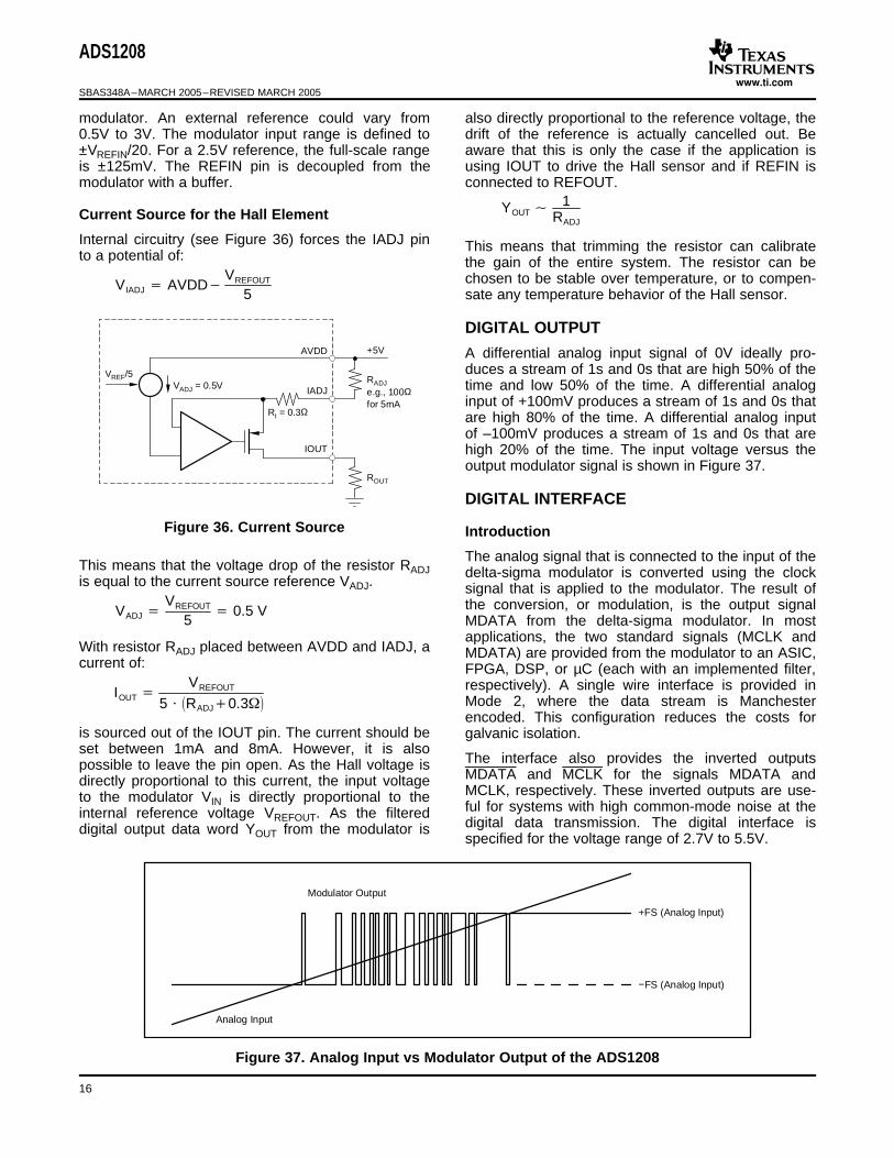
YOUT 1
RADJ
V IADJ AVDD
VREFOUT
5
DIGITAL OUTPUT
DIGITAL INTERFACE
RI = 0.3Ω
AVDD
IADJ
IOUT
VREF/5RADJe.g., 100Ωfor 5mA
+5V
ROUT
VADJ = 0.5V
Introduction
VADJ VREFOUT
5 0.5 V
IOUT VREFOUT
5 RADJ0.3
Modulator Output
Analog Input
+FS (Analog Input)
−FS (Analog Input)
ADS1208
SBAS348A–MARCH 2005–REVISED MARCH 2005
modulator. An external reference could vary from also directly proportional to the reference voltage, the0.5V to 3V. The modulator input range is defined to drift of the reference is actually cancelled out. Be±VREFIN/20. For a 2.5V reference, the full-scale range aware that this is only the case if the application isis ±125mV. The REFIN pin is decoupled from the using IOUT to drive the Hall sensor and if REFIN ismodulator with a buffer. connected to REFOUT.
Current Source for the Hall Element
Internal circuitry (see Figure 36) forces the IADJ pin This means that trimming the resistor can calibrateto a potential of: the gain of the entire system. The resistor can be
chosen to be stable over temperature, or to compen-sate any temperature behavior of the Hall sensor.
A differential analog input signal of 0V ideally pro-duces a stream of 1s and 0s that are high 50% of thetime and low 50% of the time. A differential analoginput of +100mV produces a stream of 1s and 0s thatare high 80% of the time. A differential analog inputof –100mV produces a stream of 1s and 0s that arehigh 20% of the time. The input voltage versus theoutput modulator signal is shown in Figure 37.
Figure 36. Current Source
The analog signal that is connected to the input of theThis means that the voltage drop of the resistor RADJ delta-sigma modulator is converted using the clockis equal to the current source reference VADJ. signal that is applied to the modulator. The result of
the conversion, or modulation, is the output signalMDATA from the delta-sigma modulator. In mostapplications, the two standard signals (MCLK and
With resistor RADJ placed between AVDD and IADJ, a MDATA) are provided from the modulator to an ASIC,current of: FPGA, DSP, or µC (each with an implemented filter,
respectively). A single wire interface is provided inMode 2, where the data stream is Manchesterencoded. This configuration reduces the costs for
is sourced out of the IOUT pin. The current should be galvanic isolation.set between 1mA and 8mA. However, it is also
The interface also provides the inverted outputspossible to leave the pin open. As the Hall voltage isMDATA and MCLK for the signals MDATA anddirectly proportional to this current, the input voltageMCLK, respectively. These inverted outputs are use-to the modulator VIN is directly proportional to theful for systems with high common-mode noise at theinternal reference voltage VREFOUT. As the filtereddigital data transmission. The digital interface isdigital output data word YOUT from the modulator isspecified for the voltage range of 2.7V to 5.5V.
Figure 37. Analog Input vs Modulator Output of the ADS1208
16
www.ti.com
Different Modes of Operation
Filter Usage
H(z) 1zOSR
1z1
3
(1)
ADS1208
SBAS348A–MARCH 2005–REVISED MARCH 2005
Mode 2
In Mode 2, the internal RC oscillator is running. TheThe typical system clock of the ADS1208 is 20MHz.data is Manchester encoded and is provided at theThe system clock can be provided either from theMDATA and MDATA pins. There is no clock output ininternal 20MHz RC oscillator or from an externalthis mode. The MCLK and MCLK outputs are set toclock source. For this reason, the MCLK pin islow. The Manchester coding allows the data transferbidirectional and is controlled by the mode setting.with only a single wire. See Figure 3 on page 6.The system clock is divided by two for the modulator
clock. Therefore, the default clock frequency of theMode 3modulator is 10MHz. With a possible external clock
range of 1MHz to 24MHz, the modulator operates In Mode 3, the internal RC oscillator is disabled. Thebetween 500kHz and 12MHz. The four modes of system clock must be provided externally at the inputoperation for the digital data interface are shown in MCLK. The system clock must have twice the fre-Table 2. quency of the chosen modulator clock. The data is
provided at the MDATA and MDATA output pins.Mode 0 Since the modulator runs with half the frequency of
the system clock, the data changes at every otherIn Mode 0, the internal RC oscillator is running. Thefalling edge of the external clock. The data can bedata is provided at the MDATA and MDATA outputsafely strobed at every rising edge of the MCLKpins, and the modulator clock at the MCLK andoutput, which provides half the frequency of theMCLK pins. The data changes at the falling edge ofsystem clock. This mode allows synchronous oper-MCLK. Therefore, it can safely be strobed with theation to any digital system or the use of modulatorrising edge. See Figure 1 on page 5.clocks different from 10MHz. See Figure 4 on page 6.
Mode 1
In Mode 1, the internal RC oscillator is running. TheThe modulator generates only a bitstream, which isdata is provided at the MDATA and MDATA outputdifferent from the digital word of an analog-to-digitalpins. The frequency at the MCLK and MCLK pins isconverter (ADC). In order to output a digital wordequivalent to the modulator clock frequency dividedequivalent to the analog input voltage, the bitstreamby two. The data must be strobed at both the risingmust be processed by a digital filter. A very simpleand falling edges of MCLK. The data at MDATAfilter built with minimal effort and hardware is thechanges in the middle, between the rising and fallingSinc3 filter, shown in Equation 1:edge. In this mode, the frequency of both MCLK and
MDATA is only 5MHz. See Figure 2 on page 5.
Table 2. Operating Mode Definition and Description
MODE DEFINITION M1 M0
Mode 0 Internal clock, synchronous data output Low Low
Mode 1 Internal clock, synchronous data output, half output clock frequency Low High
Mode 2 Internal clock, Manchester encoded data output, no clock output High Low
Mode 3 External clock, synchronous data output High High
17
www.ti.com
Decimation Ratio (OSR)
EN
OB
(BIts
)
1 10 100 1000
16
14
12
10
8
6
4
2
0
Sinc1
Sinc2
Sinc3
Sincfast
0
−10
−20
−30
−40
−50
−60
−70
−80
Gai
n(d
B)
Frequency (kHz)0 200 400 600 800 1000 1200 1400 1600
OSR = 32fDATA = 10MHz/32 = 312.5kHz−3dB: 81.9kHz
H(z) 1zOSR
1z1
2
1z2OSR(2)
10
9
8
7
6
5
4
3
2
1
0
EN
OB
(Bits
)
Settling Time (µs)1 2 3 4 5 6 7 8 90 10
Sinc2
Sinc
Sinc3
Sincfast
30k
25k
20k
15k
10k
5k
0
Out
put
Cod
e
Number of Output Clocks0 5 10 15 20 25 30 35 40
OSR = 32FSR = 32768ENOB = 9.9 BitsSettling Time =3 × 1/fDATA = 9.6µs
ADS1208
SBAS348A–MARCH 2005–REVISED MARCH 2005
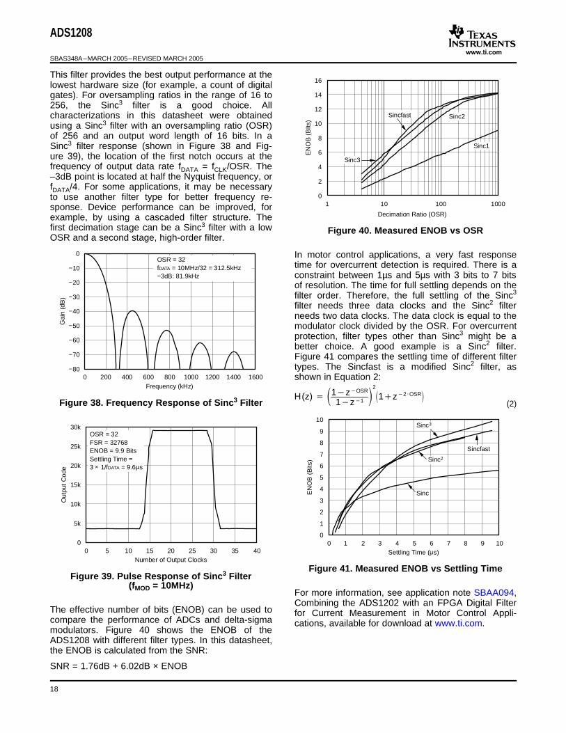
This filter provides the best output performance at thelowest hardware size (for example, a count of digitalgates). For oversampling ratios in the range of 16 to256, the Sinc3 filter is a good choice. Allcharacterizations in this datasheet were obtainedusing a Sinc3 filter with an oversampling ratio (OSR)of 256 and an output word length of 16 bits. In aSinc3 filter response (shown in Figure 38 and Fig-ure 39), the location of the first notch occurs at thefrequency of output data rate fDATA = fCLK/OSR. The–3dB point is located at half the Nyquist frequency, orfDATA/4. For some applications, it may be necessaryto use another filter type for better frequency re-sponse. Device performance can be improved, forexample, by using a cascaded filter structure. Thefirst decimation stage can be a Sinc3 filter with a low Figure 40. Measured ENOB vs OSROSR and a second stage, high-order filter.
In motor control applications, a very fast responsetime for overcurrent detection is required. There is aconstraint between 1µs and 5µs with 3 bits to 7 bitsof resolution. The time for full settling depends on thefilter order. Therefore, the full settling of the Sinc3
filter needs three data clocks and the Sinc2 filterneeds two data clocks. The data clock is equal to themodulator clock divided by the OSR. For overcurrentprotection, filter types other than Sinc3 might be abetter choice. A good example is a Sinc2 filter.Figure 41 compares the settling time of different filtertypes. The Sincfast is a modified Sinc2 filter, asshown in Equation 2:
Figure 38. Frequency Response of Sinc3 Filter
Figure 41. Measured ENOB vs Settling TimeFigure 39. Pulse Response of Sinc3 Filter
(fMOD = 10MHz)For more information, see application note SBAA094,Combining the ADS1202 with an FPGA Digital Filter
The effective number of bits (ENOB) can be used to for Current Measurement in Motor Control Appli-compare the performance of ADCs and delta-sigma cations, available for download at www.ti.com.modulators. Figure 40 shows the ENOB of theADS1208 with different filter types. In this datasheet,the ENOB is calculated from the SNR:
SNR = 1.76dB + 6.02dB × ENOB
18
www.ti.com
GroundingLAYOUT CONSIDERATIONS
Power Supplies
Decoupling
ADS1208
SBAS348A–MARCH 2005–REVISED MARCH 2005
Analog and digital sections of the system design mustbe carefully and cleanly partitioned. Each sectionshould have its own ground plane, with no overlapThe ADS1208 has two power supplies, AVDD andbetween them. Do not join the ground planes. In-BVDD. If there are separate analog and digital powerstead, connect the two planes with a moderate signalsupplies on the board, a good design approach is totrace underneath the modulator. For multiple modu-have AVDD connected to the analog and BVDD tolators, connect the two ground planes as close asthe digital power supply. Another possible approachpossible to one central location for all of the modu-to control noise is the use of a resistor on the powerlators. In some cases, experimentation may be re-supply. The connection can be made between thequired to find the best point to connect the two planesADS1208 power supply pins via a 5Ω resistor. Thetogether.combination of this resistor and the decoupling ca-
pacitors between the power supply pins AVDD andAGND provides some filtering. The analog supplymust be well-regulated and offer low noise. For Good decoupling practices must be used for thedesigns requiring higher resolution from the ADS1208 and for all components in the systemADS1208, power-supply rejection will be a concern. design. All decoupling capacitors, specifically theThe digital power supply has high-frequency noise 0.1µF ceramic capacitors, must be placed as close asthat can be coupled into the analog portion of the possible to the respective pin being decoupled. A 1µFADS1208. This noise can originate from switching and 10µF capacitor, in parallel with the 0.1µF ceramicpower supplies, microprocessors, or DSPs. capacitor, can be used to decouple AVDD to AGND.High-frequency noise will generally be rejected by the At least one 0.1µF ceramic capacitor must be used toexternal digital filter at integer multiples of MCLK. decouple BVDD to BGND, as well as for the digitalJust below and above these frequencies, noise will supply on each digital componentalias back into the passband of the digital filter,affecting the conversion result. Inputs to the It is highly recommended to place the 100nF com-ADS1208, such as VIN+, VIN- and MCLK should not be pensation capacitor, which is connected betweenpresent before the power supply is turned on. Viol- AVDD and AGND, directly at pins 3 and 6. Otherwise,ating this condition could cause latch-up. If these current glitches from the internal circuitry can causesignals are present before the supply is turned on, glitches in the supply, which again causes jitter on theseries resistors should be used to limit the input internal clock signal. This jitter degrades the noisecurrent. Additional user testing may be necessary in performance of the ADS1208. The input signals VIN+order to determine the appropriate connection be- and VIN– can be routed underneath this capacitor.tween the ADS1208 and different power supplies.
19
PACKAGE OPTION ADDENDUM
www.ti.com 31-Oct-2013
Addendum-Page 1
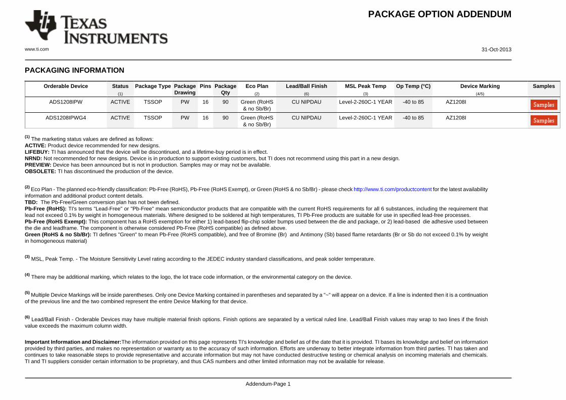
PACKAGING INFORMATION
Orderable Device Status(1)
Package Type PackageDrawing
Pins PackageQty
Eco Plan(2)
Lead/Ball Finish(6)
MSL Peak Temp(3)
Op Temp (°C) Device Marking(4/5)
Samples
ADS1208IPW ACTIVE TSSOP PW 16 90 Green (RoHS& no Sb/Br)
CU NIPDAU Level-2-260C-1 YEAR -40 to 85 AZ1208I
ADS1208IPWG4 ACTIVE TSSOP PW 16 90 Green (RoHS& no Sb/Br)
CU NIPDAU Level-2-260C-1 YEAR -40 to 85 AZ1208I
(1) The marketing status values are defined as follows:ACTIVE: Product device recommended for new designs.LIFEBUY: TI has announced that the device will be discontinued, and a lifetime-buy period is in effect.NRND: Not recommended for new designs. Device is in production to support existing customers, but TI does not recommend using this part in a new design.PREVIEW: Device has been announced but is not in production. Samples may or may not be available.OBSOLETE: TI has discontinued the production of the device.
(2) Eco Plan - The planned eco-friendly classification: Pb-Free (RoHS), Pb-Free (RoHS Exempt), or Green (RoHS & no Sb/Br) - please check http://www.ti.com/productcontent for the latest availabilityinformation and additional product content details.TBD: The Pb-Free/Green conversion plan has not been defined.Pb-Free (RoHS): TI's terms "Lead-Free" or "Pb-Free" mean semiconductor products that are compatible with the current RoHS requirements for all 6 substances, including the requirement thatlead not exceed 0.1% by weight in homogeneous materials. Where designed to be soldered at high temperatures, TI Pb-Free products are suitable for use in specified lead-free processes.Pb-Free (RoHS Exempt): This component has a RoHS exemption for either 1) lead-based flip-chip solder bumps used between the die and package, or 2) lead-based die adhesive used betweenthe die and leadframe. The component is otherwise considered Pb-Free (RoHS compatible) as defined above.Green (RoHS & no Sb/Br): TI defines "Green" to mean Pb-Free (RoHS compatible), and free of Bromine (Br) and Antimony (Sb) based flame retardants (Br or Sb do not exceed 0.1% by weightin homogeneous material)
(3) MSL, Peak Temp. - The Moisture Sensitivity Level rating according to the JEDEC industry standard classifications, and peak solder temperature.
(4) There may be additional marking, which relates to the logo, the lot trace code information, or the environmental category on the device.
(5) Multiple Device Markings will be inside parentheses. Only one Device Marking contained in parentheses and separated by a "~" will appear on a device. If a line is indented then it is a continuationof the previous line and the two combined represent the entire Device Marking for that device.
(6) Lead/Ball Finish - Orderable Devices may have multiple material finish options. Finish options are separated by a vertical ruled line. Lead/Ball Finish values may wrap to two lines if the finishvalue exceeds the maximum column width.
Important Information and Disclaimer:The information provided on this page represents TI's knowledge and belief as of the date that it is provided. TI bases its knowledge and belief on informationprovided by third parties, and makes no representation or warranty as to the accuracy of such information. Efforts are underway to better integrate information from third parties. TI has taken andcontinues to take reasonable steps to provide representative and accurate information but may not have conducted destructive testing or chemical analysis on incoming materials and chemicals.TI and TI suppliers consider certain information to be proprietary, and thus CAS numbers and other limited information may not be available for release.
PACKAGE OPTION ADDENDUM
www.ti.com 31-Oct-2013
Addendum-Page 2
In no event shall TI's liability arising out of such information exceed the total purchase price of the TI part(s) at issue in this document sold by TI to Customer on an annual basis.
IMPORTANT NOTICE
Texas Instruments Incorporated and its subsidiaries (TI) reserve the right to make corrections, enhancements, improvements and otherchanges to its semiconductor products and services per JESD46, latest issue, and to discontinue any product or service per JESD48, latestissue. Buyers should obtain the latest relevant information before placing orders and should verify that such information is current andcomplete. All semiconductor products (also referred to herein as “components”) are sold subject to TI’s terms and conditions of salesupplied at the time of order acknowledgment.TI warrants performance of its components to the specifications applicable at the time of sale, in accordance with the warranty in TI’s termsand conditions of sale of semiconductor products. Testing and other quality control techniques are used to the extent TI deems necessaryto support this warranty. Except where mandated by applicable law, testing of all parameters of each component is not necessarilyperformed.TI assumes no liability for applications assistance or the design of Buyers’ products. Buyers are responsible for their products andapplications using TI components. To minimize the risks associated with Buyers’ products and applications, Buyers should provideadequate design and operating safeguards.TI does not warrant or represent that any license, either express or implied, is granted under any patent right, copyright, mask work right, orother intellectual property right relating to any combination, machine, or process in which TI components or services are used. Informationpublished by TI regarding third-party products or services does not constitute a license to use such products or services or a warranty orendorsement thereof. Use of such information may require a license from a third party under the patents or other intellectual property of thethird party, or a license from TI under the patents or other intellectual property of TI.Reproduction of significant portions of TI information in TI data books or data sheets is permissible only if reproduction is without alterationand is accompanied by all associated warranties, conditions, limitations, and notices. TI is not responsible or liable for such altereddocumentation. Information of third parties may be subject to additional restrictions.Resale of TI components or services with statements different from or beyond the parameters stated by TI for that component or servicevoids all express and any implied warranties for the associated TI component or service and is an unfair and deceptive business practice.TI is not responsible or liable for any such statements.Buyer acknowledges and agrees that it is solely responsible for compliance with all legal, regulatory and safety-related requirementsconcerning its products, and any use of TI components in its applications, notwithstanding any applications-related information or supportthat may be provided by TI. Buyer represents and agrees that it has all the necessary expertise to create and implement safeguards whichanticipate dangerous consequences of failures, monitor failures and their consequences, lessen the likelihood of failures that might causeharm and take appropriate remedial actions. Buyer will fully indemnify TI and its representatives against any damages arising out of the useof any TI components in safety-critical applications.In some cases, TI components may be promoted specifically to facilitate safety-related applications. With such components, TI’s goal is tohelp enable customers to design and create their own end-product solutions that meet applicable functional safety standards andrequirements. Nonetheless, such components are subject to these terms.No TI components are authorized for use in FDA Class III (or similar life-critical medical equipment) unless authorized officers of the partieshave executed a special agreement specifically governing such use.Only those TI components which TI has specifically designated as military grade or “enhanced plastic” are designed and intended for use inmilitary/aerospace applications or environments. Buyer acknowledges and agrees that any military or aerospace use of TI componentswhich have not been so designated is solely at the Buyer's risk, and that Buyer is solely responsible for compliance with all legal andregulatory requirements in connection with such use.TI has specifically designated certain components as meeting ISO/TS16949 requirements, mainly for automotive use. In any case of use ofnon-designated products, TI will not be responsible for any failure to meet ISO/TS16949.
Products ApplicationsAudio www.ti.com/audio Automotive and Transportation www.ti.com/automotiveAmplifiers amplifier.ti.com Communications and Telecom www.ti.com/communicationsData Converters dataconverter.ti.com Computers and Peripherals www.ti.com/computersDLP® Products www.dlp.com Consumer Electronics www.ti.com/consumer-appsDSP dsp.ti.com Energy and Lighting www.ti.com/energyClocks and Timers www.ti.com/clocks Industrial www.ti.com/industrialInterface interface.ti.com Medical www.ti.com/medicalLogic logic.ti.com Security www.ti.com/securityPower Mgmt power.ti.com Space, Avionics and Defense www.ti.com/space-avionics-defenseMicrocontrollers microcontroller.ti.com Video and Imaging www.ti.com/videoRFID www.ti-rfid.comOMAP Applications Processors www.ti.com/omap TI E2E Community e2e.ti.comWireless Connectivity www.ti.com/wirelessconnectivity
Mailing Address: Texas Instruments, Post Office Box 655303, Dallas, Texas 75265Copyright © 2015, Texas Instruments Incorporated