Embed Size (px)
Citation preview
Description
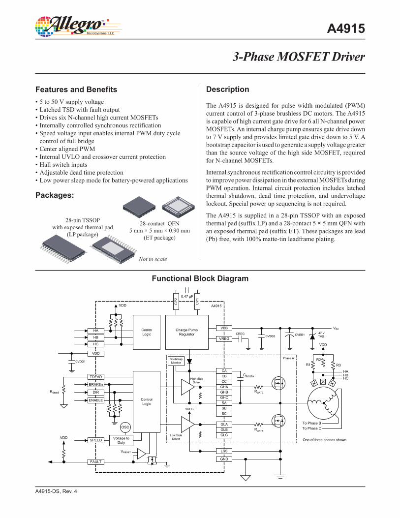
The A4915 is designed for pulse width modulated (PWM) current control of 3-phase brushless DC motors. The A4915 is capable of high current gate drive for 6 all N-channel power MOSFETs. An internal charge pump ensures gate drive down to 7 V supply and provides limited gate drive down to 5 V. A bootstrap capacitor is used to generate a supply voltage greater than the source voltage of the high side MOSFET, required for N-channel MOSFETs.
Internal synchronous rectification control circuitry is provided to improve power dissipation in the external MOSFETs during PWM operation. Internal circuit protection includes latched thermal shutdown, dead time protection, and undervoltage lockout. Special power up sequencing is not required.
The A4915 is supplied in a 28-pin TSSOP with an exposed thermal pad (suffix LP) and a 28-contact 5 × 5 mm QFN with an exposed thermal pad (suffix ET). These packages are lead (Pb) free, with 100% matte-tin leadframe plating.
A4915-DS, Rev. 4
Features and Benefits• 5 to 50 V supply voltage• Latched TSD with fault output• Drives six N-channel high current MOSFETs• Internally controlled synchronous rectification• Speed voltage input enables internal PWM duty cycle
control of full bridge• Center aligned PWM• Internal UVLO and crossover current protection• Hall switch inputs• Adjustable dead time protection• Low power sleep mode for battery-powered applications
3-Phase MOSFET Driver
Packages:
Functional Block Diagram
Not to scale
A4915
28-contact QFN5 mm × 5 mm × 0.90 mm
(ET package)
28-pin TSSOP with exposed thermal pad
(LP package)
Charge Pump Regulator
CommLogic
DIR
HB
HC
HA
BRAKEn
ENABLE
GLA
GHA
VBB
CP
1
CP
2
ControlLogic
GND
VIN
SA
GHB
SB
GLB
GHC
SC
GLCSPEED
0.47 µF
RGATE
RGATE
CACBOOTA
To Phase BTo Phase C
LSS
CBCC
BootstrapMonitor
VREG
VREGCREG CVBB1CVBB2
HAHBHC
R1R2
R3
Phase A
One of three phases shown
High SideDriver
Low SideDriver
VDD
TDEAD
Rdead
47 VTVS
Voltage to Duty
OSC
FAULT
VRESET
CVDD1
VDD
VDD
A4915VDD
3-Phase MOSFET DriverA4915
2Allegro MicroSystems, LLC115 Northeast CutoffWorcester, Massachusetts 01615-0036 U.S.A.1.508.853.5000; www.allegromicro.com
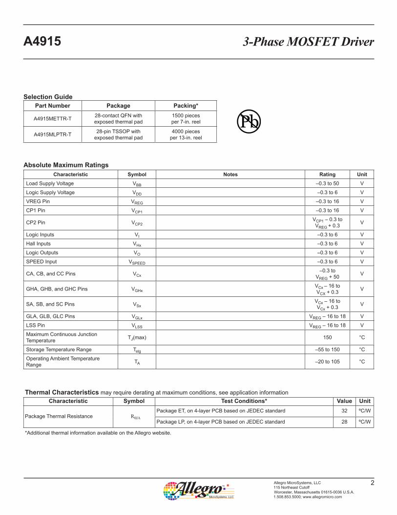
Absolute Maximum RatingsCharacteristic Symbol Notes Rating Unit
Load Supply Voltage VBB –0.3 to 50 V
Logic Supply Voltage VDD –0.3 to 6 V
VREG Pin VREG –0.3 to 16 V
CP1 Pin VCP1 –0.3 to 16 V
CP2 Pin VCP2VCP1 – 0.3 to VREG + 0.3 V
Logic Inputs VI –0.3 to 6 V
Hall Inputs VHx –0.3 to 6 V
Logic Outputs VO –0.3 to 6 V
SPEED Input VSPEED –0.3 to 6 V
CA, CB, and CC Pins VCx–0.3 to
VREG + 50 V
GHA, GHB, and GHC Pins VGHx VCx – 16 to VCX + 0.3 V
SA, SB, and SC Pins VSxVCx – 16 to VCx + 0.3 V
GLA, GLB, GLC Pins VGLx VREG – 16 to 18 V
LSS Pin VLSS VREG – 16 to 18 V
Maximum Continuous Junction Temperature TJ(max) 150 °C
Storage Temperature Range Tstg –55 to 150 °C
Operating Ambient Temperature Range TA –20 to 105 °C
Thermal Characteristics may require derating at maximum conditions, see application informationCharacteristic Symbol Test Conditions* Value Unit
Package Thermal Resistance RθJA
Package ET, on 4-layer PCB based on JEDEC standard 32 ºC/W
Package LP, on 4-layer PCB based on JEDEC standard 28 ºC/W
*Additional thermal information available on the Allegro website.
Selection GuidePart Number Package Packing*
A4915METTR-T 28-contact QFN with exposed thermal pad
1500 pieces per 7-in. reel
A4915MLPTR-T 28-pin TSSOP with exposed thermal pad
4000 pieces per 13-in. reel
3-Phase MOSFET DriverA4915
3Allegro MicroSystems, LLC115 Northeast CutoffWorcester, Massachusetts 01615-0036 U.S.A.1.508.853.5000; www.allegromicro.com
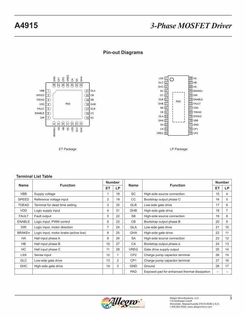
Terminal List Table
Name FunctionNumber
Name FunctionNumber
ET LP ET LPVBB Supply voltage 1 18 SC High-side source connection 15 4
SPEED Reference voltage input 2 19 CC Bootstrap output phase C 16 5
TDEAD Terminal for dead time setting 3 20 GLB Low-side gate drive 17 6
VDD Logic supply input 4 21 GHB High-side gate drive 18 7
FAULT Fault output 5 22 SB High-side source connection 19 8
ENABLE Logic input, PWM control 6 23 CB Bootstrap output phase B 20 9
DIR Logic input, motor direction 7 24 GLA Low-side gate drive 21 10
BRAKEn Logic input, motor brake (active low) 8 25 GHA High-side gate drive 22 11
HA Hall input phase A 9 26 SA High-side source connection 23 12
HB Hall input phase B 10 27 CA Bootstrap output phase a 24 13
HC Hall input phase C 11 28 VREG Gate drive supply output 25 14
LSS Sense input 12 1 CP2 Charge pump capacitor terminal 26 15
GLC Low-side gate drive 13 2 CP1 Charge pump capacitor terminal 27 16
GHC High-side gate drive 14 3 GND Ground 28 17
PAD Exposed pad for enhanced thermal dissipation – –
PAD
21
20
19
18
17
16
15
1
2
3
4
5
6
7
8 9 10 11 12 13 14
28 27 26 25 24 23 22
GN
D
CP
1
CP
2
VR
EG
CA
SA
GH
A
BR
AK
En
HA
HB
HC
LSS
GLC
GH
C
GLA
CB
SB
GHB
GLB
CC
SC
VBB
SPEED
TDEAD
VDD
FAULT
ENABLE
DIR
LSS
GLC
GHC
SC
CC
GLB
GHB
SB
CB
GLA
GHA
SA
CA
VREG
HC
HB
HA
BRAKEn
DIR
ENABLE
FAULT
VDD
TDEAD
SPEED
VBB
GND
CP1
CP2
1
2
3
4
5
6
7
8
9
10
11
12
13
14
28
27
26
25
24
23
22
21
20
19
18
17
16
15
PAD
Pin-out Diagrams
ET Package LP Package
3-Phase MOSFET DriverA4915
4Allegro MicroSystems, LLC115 Northeast CutoffWorcester, Massachusetts 01615-0036 U.S.A.1.508.853.5000; www.allegromicro.com
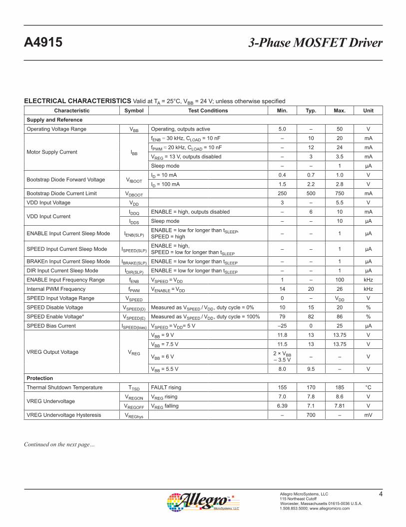
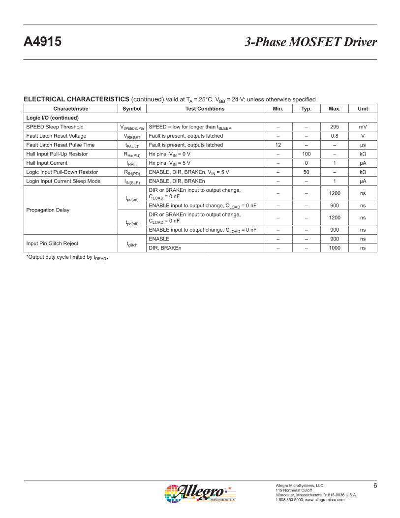
ELECTRICAL CHARACTERISTICS Valid at TA = 25°C, VBB = 24 V; unless otherwise specifiedCharacteristic Symbol Test Conditions Min. Typ. Max. Unit
Supply and ReferenceOperating Voltage Range VBB Operating, outputs active 5.0 – 50 V
Motor Supply Current IBB
fENB = 30 kHz, CLOAD = 10 nF – 10 20 mA
fPWM ≈ 20 kHz, CLOAD = 10 nF – 12 24 mA
VREG = 13 V, outputs disabled – 3 3.5 mA
Sleep mode – – 1 µA
Bootstrap Diode Forward Voltage VfBOOTID = 10 mA 0.4 0.7 1.0 V
ID = 100 mA 1.5 2.2 2.8 V
Bootstrap Diode Current Limit VDBOOT 250 500 750 mA
VDD Input Voltage VDD 3 – 5.5 V
VDD Input CurrentIDDQ ENABLE = high, outputs disabled – 6 10 mA
IDDS Sleep mode – – 10 µA
ENABLE Input Current Sleep Mode IENB(SLP)ENABLE = low for longer than tSLEEP, SPEED = high – – 1 µA
SPEED Input Current Sleep Mode ISPEED(SLP)ENABLE = high, SPEED = low for longer than tSLEEP
– – 1 µA
BRAKEn Input Current Sleep Mode IBRAKE(SLP) ENABLE = low for longer than tSLEEP – – 1 µA
DIR Input Current Sleep Mode IDIR(SLP) ENABLE = low for longer than tSLEEP – – 1 µA
ENABLE Input Frequency Range fENB VSPEED = VDD 1 – 100 kHz
Internal PWM Frequency fPWM VENABLE = VDD 14 20 26 kHz
SPEED Input Voltage Range VSPEED 0 – VDD V
SPEED Disable Voltage VSPEED(D) Measured as VSPEED / VDD , duty cycle = 0% 10 15 20 %
SPEED Enable Voltage* VSPEED(E) Measured as VSPEED / VDD , duty cycle = 100% 79 82 86 %
SPEED Bias Current ISPEED(bias) VSPEED = VDD= 5 V –25 0 25 µA
VREG Output Voltage VREG
VBB = 9 V 11.8 13 13.75 V
VBB = 7.5 V 11.5 13 13.75 V
VBB = 6 V 2 × VBB – 3.5 V – – V
VBB = 5.5 V 8.0 9.5 – V
ProtectionThermal Shutdown Temperature TTSD FAULT rising 155 170 185 °C
VREG UndervoltageVREGON VREG rising 7.0 7.8 8.6 V
VREGOFF VREG falling 6.39 7.1 7.81 V
VREG Undervoltage Hysteresis VREGhys – 700 – mV
Continued on the next page…
3-Phase MOSFET DriverA4915
5Allegro MicroSystems, LLC115 Northeast CutoffWorcester, Massachusetts 01615-0036 U.S.A.1.508.853.5000; www.allegromicro.com
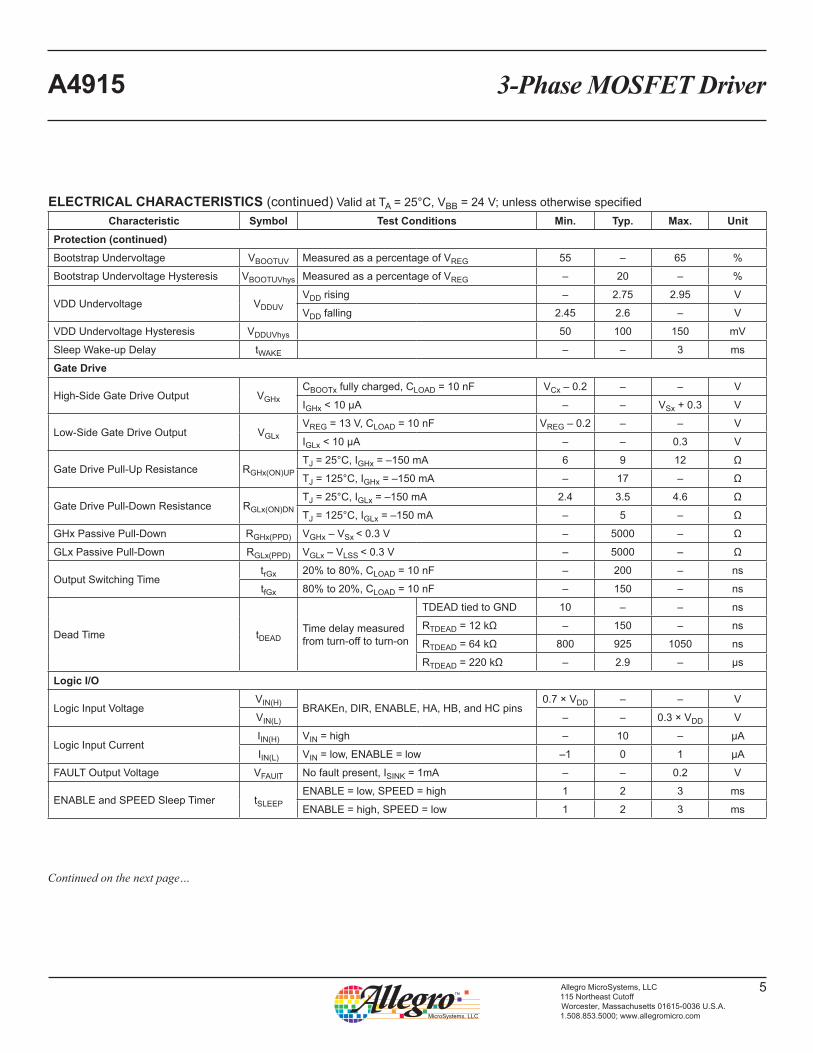
Protection (continued)Bootstrap Undervoltage VBOOTUV Measured as a percentage of VREG 55 – 65 %
Bootstrap Undervoltage Hysteresis VBOOTUVhys Measured as a percentage of VREG – 20 – %
VDD Undervoltage VDDUVVDD rising – 2.75 2.95 V
VDD falling 2.45 2.6 – V
VDD Undervoltage Hysteresis VDDUVhys 50 100 150 mV
Sleep Wake-up Delay tWAKE – – 3 ms
Gate Drive
High-Side Gate Drive Output VGHxCBOOTx fully charged, CLOAD = 10 nF VCx – 0.2 – – V
IGHx < 10 µA – – VSx + 0.3 V
Low-Side Gate Drive Output VGLxVREG = 13 V, CLOAD = 10 nF VREG – 0.2 – – V
IGLx < 10 µA – – 0.3 V
Gate Drive Pull-Up Resistance RGHx(ON)UPTJ = 25°C, IGHx = –150 mA 6 9 12 Ω
TJ = 125°C, IGHx = –150 mA – 17 – Ω
Gate Drive Pull-Down Resistance RGLx(ON)DNTJ = 25°C, IGLx = –150 mA 2.4 3.5 4.6 Ω
TJ = 125°C, IGLx = –150 mA – 5 – Ω
GHx Passive Pull-Down RGHx(PPD) VGHx – VSx < 0.3 V – 5000 – Ω
GLx Passive Pull-Down RGLx(PPD) VGLx – VLSS < 0.3 V – 5000 – Ω
Output Switching TimetrGx 20% to 80%, CLOAD = 10 nF – 200 – ns
tfGx 80% to 20%, CLOAD = 10 nF – 150 – ns
Dead Time tDEADTime delay measured from turn-off to turn-on
TDEAD tied to GND 10 – – ns
RTDEAD = 12 kΩ – 150 – ns
RTDEAD = 64 kΩ 800 925 1050 ns
RTDEAD = 220 kΩ – 2.9 – µs
Logic I/O
Logic Input VoltageVIN(H) BRAKEn, DIR, ENABLE, HA, HB, and HC pins
0.7 × VDD – – V
VIN(L) – – 0.3 × VDD V
Logic Input CurrentIIN(H) VIN = high – 10 – µA
IIN(L) VIN = low, ENABLE = low –1 0 1 µA
FAULT Output Voltage VFAUlT No fault present, ISINK = 1mA – – 0.2 V
ENABLE and SPEED Sleep Timer tSLEEPENABLE = low, SPEED = high 1 2 3 ms
ENABLE = high, SPEED = low 1 2 3 ms
ELECTRICAL CHARACTERISTICS (continued) Valid at TA = 25°C, VBB = 24 V; unless otherwise specifiedCharacteristic Symbol Test Conditions Min. Typ. Max. Unit
Continued on the next page…
3-Phase MOSFET DriverA4915
6Allegro MicroSystems, LLC115 Northeast CutoffWorcester, Massachusetts 01615-0036 U.S.A.1.508.853.5000; www.allegromicro.com
ELECTRICAL CHARACTERISTICS (continued) Valid at TA = 25°C, VBB = 24 V; unless otherwise specifiedCharacteristic Symbol Test Conditions Min. Typ. Max. Unit
Logic I/O (continued)SPEED Sleep Threshold VSPEEDSLPth SPEED = low for longer than tSLEEP – – 295 mV
Fault Latch Reset Voltage VRESET Fault is present, outputs latched – – 0.8 V
Fault Latch Reset Pulse Time tFAULT Fault is present, outputs latched 12 – – µs
Hall Input Pull-Up Resistor RHx(PU) Hx pins, VIN = 0 V – 100 – kΩ
Hall Input Current IHALL Hx pins, VIN = 5 V – 0 1 µA
Logic Input Pull-Down Resistor RIN(PD) ENABLE, DIR, BRAKEn, VIN = 5 V – 50 – kΩ
Login Input Current Sleep Mode IIN(SLP) ENABLE, DIR, BRAKEn – – 1 µA
Propagation Delay
tpd(on)
DIR or BRAKEn input to output change, CLOAD = 0 nF – – 1200 ns
ENABLE input to output change, CLOAD = 0 nF – – 900 ns
tpd(off)
DIR or BRAKEn input to output change, CLOAD = 0 nF – – 1200 ns
ENABLE input to output change, CLOAD = 0 nF – – 900 ns
Input Pin Glitch Reject tglitchENABLE – – 900 ns
DIR, BRAKEn – – 1000 ns
*Output duty cycle limited by tDEAD .
3-Phase MOSFET DriverA4915
7Allegro MicroSystems, LLC115 Northeast CutoffWorcester, Massachusetts 01615-0036 U.S.A.1.508.853.5000; www.allegromicro.com
Functional Description
Basic OperationThe A4915 is a 3-phase MOSFET driver intended to drive high current MOSFETs. It is designed for use in battery operated equipment where low-voltage operation is critical. The A4915 also features a low current sleep mode which disables the device and draws minimum supply current. The A4915 is capable of driving 6 N-channel MOSFETs. Commutation logic includes Enable, Direction, and Brake modes for external PWM control.
A Speed input is provided which allows an external source to PWM the bridge at 30 kHz typical. The PWM duty cycle is controlled by applying an analog voltage to the SPEED pin from 0 V to VDD .
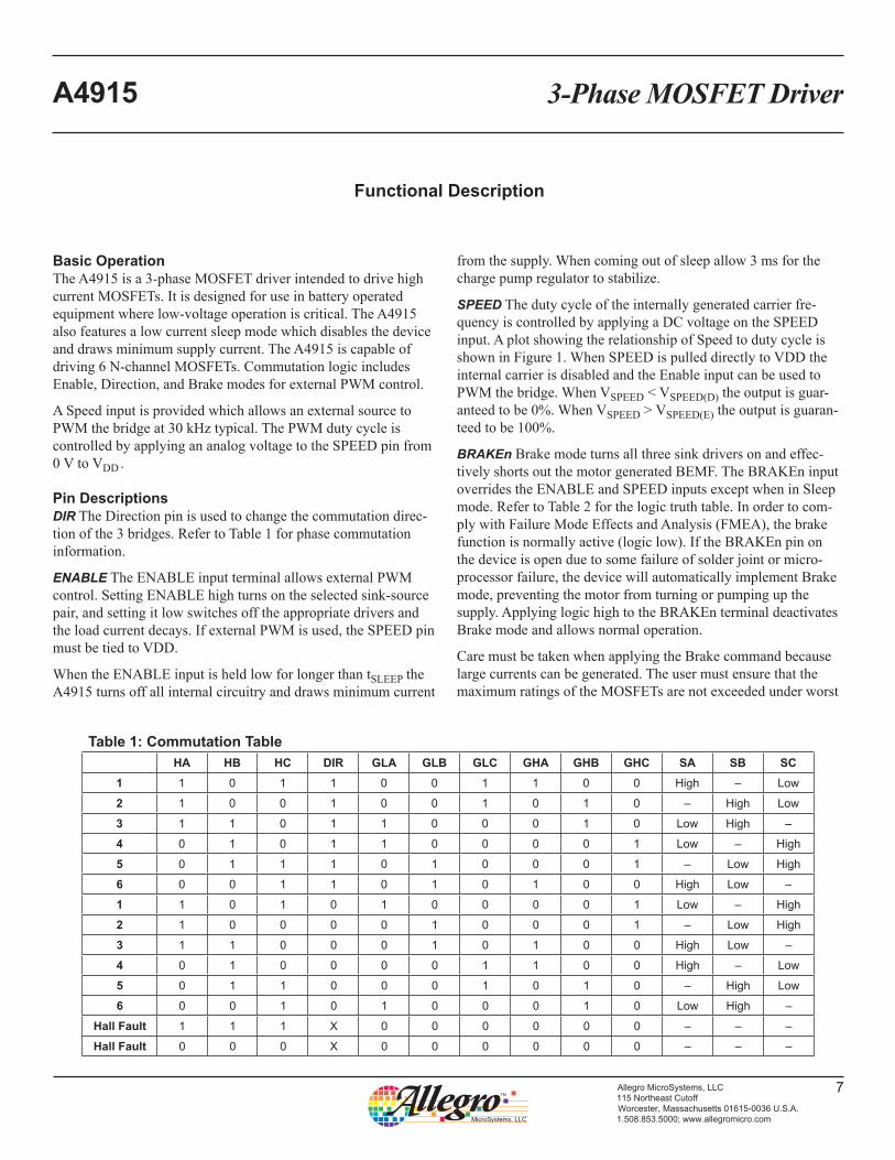
Pin DescriptionsDIR The Direction pin is used to change the commutation direc-tion of the 3 bridges. Refer to Table 1 for phase commutation information.
ENABLE The ENABLE input terminal allows external PWM control. Setting ENABLE high turns on the selected sink-source pair, and setting it low switches off the appropriate drivers and the load current decays. If external PWM is used, the SPEED pin must be tied to VDD.
When the ENABLE input is held low for longer than tSLEEP the A4915 turns off all internal circuitry and draws minimum current
from the supply. When coming out of sleep allow 3 ms for the charge pump regulator to stabilize.
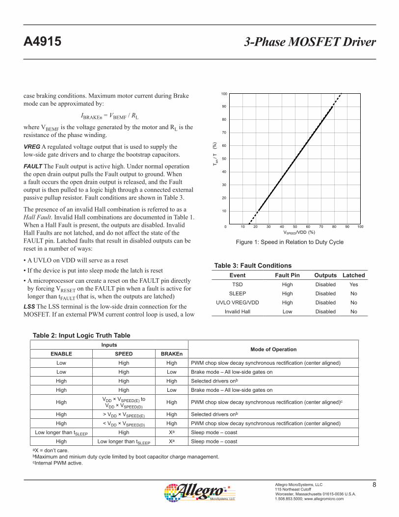
SPEED The duty cycle of the internally generated carrier fre-quency is controlled by applying a DC voltage on the SPEED input. A plot showing the relationship of Speed to duty cycle is shown in Figure 1. When SPEED is pulled directly to VDD the internal carrier is disabled and the Enable input can be used to PWM the bridge. When VSPEED < VSPEED(D) the output is guar-anteed to be 0%. When VSPEED > VSPEED(E) the output is guaran-teed to be 100%.
BRAKEn Brake mode turns all three sink drivers on and effec-tively shorts out the motor generated BEMF. The BRAKEn input overrides the ENABLE and SPEED inputs except when in Sleep mode. Refer to Table 2 for the logic truth table. In order to com-ply with Failure Mode Effects and Analysis (FMEA), the brake function is normally active (logic low). If the BRAKEn pin on the device is open due to some failure of solder joint or micro-processor failure, the device will automatically implement Brake mode, preventing the motor from turning or pumping up the supply. Applying logic high to the BRAKEn terminal deactivates Brake mode and allows normal operation.
Care must be taken when applying the Brake command because large currents can be generated. The user must ensure that the maximum ratings of the MOSFETs are not exceeded under worst
Table 1: Commutation TableHA HB HC DIR GLA GLB GLC GHA GHB GHC SA SB SC
1 1 0 1 1 0 0 1 1 0 0 High – Low
2 1 0 0 1 0 0 1 0 1 0 – High Low
3 1 1 0 1 1 0 0 0 1 0 Low High –
4 0 1 0 1 1 0 0 0 0 1 Low – High
5 0 1 1 1 0 1 0 0 0 1 – Low High
6 0 0 1 1 0 1 0 1 0 0 High Low –
1 1 0 1 0 1 0 0 0 0 1 Low – High
2 1 0 0 0 0 1 0 0 0 1 – Low High
3 1 1 0 0 0 1 0 1 0 0 High Low –
4 0 1 0 0 0 0 1 1 0 0 High – Low
5 0 1 1 0 0 0 1 0 1 0 – High Low
6 0 0 1 0 1 0 0 0 1 0 Low High –
Hall Fault 1 1 1 X 0 0 0 0 0 0 – – –
Hall Fault 0 0 0 X 0 0 0 0 0 0 – – –
3-Phase MOSFET DriverA4915
8Allegro MicroSystems, LLC115 Northeast CutoffWorcester, Massachusetts 01615-0036 U.S.A.1.508.853.5000; www.allegromicro.com
case braking conditions. Maximum motor current during Brake mode can be approximated by:
IBRAKEn = VBEMF / RL
where VBEMF is the voltage generated by the motor and RL is the resistance of the phase winding.
VREG A regulated voltage output that is used to supply the low-side gate drivers and to charge the bootstrap capacitors.
FAULT The Fault output is active high. Under normal operation the open drain output pulls the Fault output to ground. When a fault occurs the open drain output is released, and the Fault output is then pulled to a logic high through a connected external passive pullup resistor. Fault conditions are shown in Table 3.
The presence of an invalid Hall combination is referred to as a Hall Fault. Invalid Hall combinations are documented in Table 1. When a Hall Fault is present, the outputs are disabled. Invalid Hall Faults are not latched, and do not affect the state of the FAULT pin. Latched faults that result in disabled outputs can be reset in a number of ways:
• A UVLO on VDD will serve as a reset• If the device is put into sleep mode the latch is reset• A microprocessor can create a reset on the FAULT pin directly
by forcing VRESET on the FAULT pin when a fault is active for longer than tFAULT (that is, when the outputs are latched)
LSS The LSS terminal is the low-side drain connection for the MOSFET. If an external PWM current control loop is used, a low
Table 2: Input Logic Truth TableInputs
Mode of OperationENABLE SPEED BRAKEn
Low High High PWM chop slow decay synchronous rectification (center aligned)
Low High Low Brake mode – All low-side gates on
High High High Selected drivers onb
High High Low Brake mode – All low-side gates on
High VDD × VSPEED(E) to VDD × VSPEED(D)
High PWM chop slow decay synchronous rectification (center aligned)c
High > VDD × VSPEED(E) High Selected drivers onb
High < VDD × VSPEED(D) High PWM chop slow decay synchronous rectification (center aligned)
Low longer than tSLEEP High Xa Sleep mode – coast
High Low longer than tSLEEP Xa Sleep mode – coastaX = don’t care. bMaximum and minium duty cycle limited by boot capacitor charge management.cInternal PWM active.
0
10
20
30
40
50
60
70
80
90
100
10 20 30 40 50 60 70 80 90 100
T on
/T(%
)
VSPEED/VDD (%)
Figure 1: Speed in Relation to Duty Cycle
Table 3: Fault ConditionsEvent Fault Pin Outputs LatchedTSD High Disabled Yes
SLEEP High Disabled No
UVLO VREG/VDD High Disabled No
Invalid Hall Low Disabled No
3-Phase MOSFET DriverA4915
9Allegro MicroSystems, LLC115 Northeast CutoffWorcester, Massachusetts 01615-0036 U.S.A.1.508.853.5000; www.allegromicro.com
value sense resistor can be placed from LSS to ground for current sensing purposes. The resistor should be chosen so that the DC voltage across the sense resistor is between 200 mV and 500 mV. If a sense resistor is not used then LSS should be con-nected directly to power ground.
CA, CB, CC High-side connections for the bootstrap capacitors (CBOOTx) and positive supply for high-side gate drive.
GHA, GHB, GHC High-side gate drive outputs for N-channel MOSFETs.
SA, SB, SC Motor phase connections, serve as the negative sup-plies for the high-side gate drive.
GLA, GLB, GLC Low-side gate drive outputs for N-channel MOSFETs.
CP1, CP2 Connections for the charge pump switching capacitor. Typical capacitance should be 0.47 µF.
HA, HB, HC Hall input connections from Hall switches at the motor.
Thermal ShutdownIf the die temperature exceeds TTSD , the FAULT output is turned off and the outputs are disabled. Thermal shutdown is a latched fault.
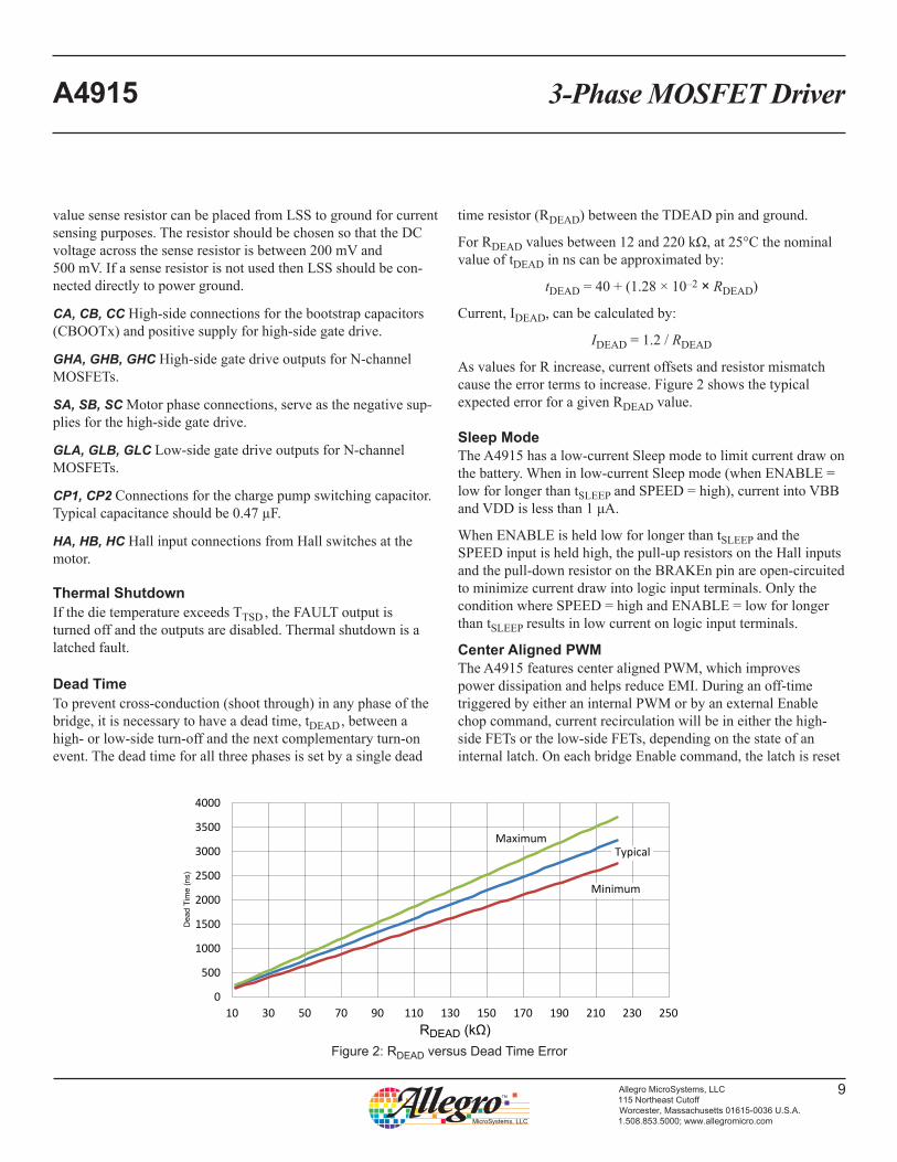
Dead TimeTo prevent cross-conduction (shoot through) in any phase of the bridge, it is necessary to have a dead time, tDEAD , between a high- or low-side turn-off and the next complementary turn-on event. The dead time for all three phases is set by a single dead
time resistor (RDEAD) between the TDEAD pin and ground.
For RDEAD values between 12 and 220 kΩ, at 25°C the nominal value of tDEAD in ns can be approximated by:
tDEAD = 40 + (1.28 × 10⁻² × RDEAD)
Current, IDEAD, can be calculated by:
IDEAD = 1.2 / RDEAD
As values for R increase, current offsets and resistor mismatch cause the error terms to increase. Figure 2 shows the typical expected error for a given RDEAD value.
Sleep ModeThe A4915 has a low-current Sleep mode to limit current draw on the battery. When in low-current Sleep mode (when ENABLE = low for longer than tSLEEP and SPEED = high), current into VBB and VDD is less than 1 μA.
When ENABLE is held low for longer than tSLEEP and the SPEED input is held high, the pull-up resistors on the Hall inputs and the pull-down resistor on the BRAKEn pin are open-circuited to minimize current draw into logic input terminals. Only the condition where SPEED = high and ENABLE = low for longer than tSLEEP results in low current on logic input terminals.
Center Aligned PWMThe A4915 features center aligned PWM, which improves power dissipation and helps reduce EMI. During an off-time triggered by either an internal PWM or by an external Enable chop command, current recirculation will be in either the high-side FETs or the low-side FETs, depending on the state of an internal latch. On each bridge Enable command, the latch is reset
0
500
1000
1500
2000
2500
3000
3500
4000
10 30 50 70 90 110 130 150 170 190 210 230 250
Dea
d Ti
me
(ns)
RDEAD (kΩ)
Typical
Minimum
Maximum
Figure 2: RDEAD versus Dead Time Error
3-Phase MOSFET DriverA4915
10Allegro MicroSystems, LLC115 Northeast CutoffWorcester, Massachusetts 01615-0036 U.S.A.1.508.853.5000; www.allegromicro.com
and the current recirculation shifts from high-side recirculation to low-side recirculation.
This method of recirculation shifts 50% of the power to the high-side drivers during the off-time, reducing the power dissipa-tion in the sink drivers. Reducing the overall temperature of the output drivers by sharing power between the 6 FETs improves system efficiency and battery life.
Internal/External PWMThe A4915 can be pulse width modulated (PWM) to control cur-rent. There are two methods by which PWM can be applied to the device.
• External PWM. This method requires a PWM signal be applied to the ENABLE pin. When the SPEED pin is tied directly to VDD, the ENABLE pin can be chopped from 0 to 100%. If the ENABLE input is held low for more than sleep timer, tSLEEP , the device enters low current sleep mode.
• Internal PWM. This method uses the internally generated PWM, which is controlled by applying a DC voltage to the SPEED pin. When the ENABLE pin is tied directly to VDD, the speed can be controlled from 0 to 100%. See the SPEED pin description for further information.
For complete description of all operating conditions, see Table 2.
Synchronous RectificationWhen a PWM off-time cycle is triggered by an ENABLE chop command or by an internal PWM off-time, load current recircu-lates. The A4915 synchronous rectification feature will turn on the appropriate MOSFETs during the off-time and effectively short out the body diodes with the low RSD(on) driver. This will lower power dissipation significantly and eliminates the need for external Schottky diodes.
Charge Pump RegulatorThe gate drives for the low-side MOSFETs and the bootstrap charge for the high-side drivers is accomplished by the charge pump regulator. For VBB above 16 V, the regulator acts as a linear regulator. Below 16 V, the regulated supply is maintained by a charge pump boost converter that requires a pump capacitor between CP1 and CP2.
The regulated voltage VREG is decoupled on the VREG termi-nal. The decoupling capacitance is based on the bootstrap capaci-tor which is dependent on the MOSFET selection. Refer to the Application Information section for details on correct sizing of VREG and bootstrap capacitors.
Gate Drive and RGATE
The gate drive for the external MOSFETs is capable of providing the large current transients needed to quickly charge and dis-charge the gate capacitance to maintain fast switching speeds and minimal power dissipation. The low-side driver current is sourced by the capacitor on the VREG terminal. The high-side gate drive current is supplied by the respective bootstrap capacitance con-nected between the Cx and Sx terminals. The charge and dis-charge of the gate can be controlled by using an external resistor (RGATE) in series with the gate.
Bootstrap Charge ManagementIn order to protect the external MOSFETs from insufficient gate drive, it is important that the bootstrap capacitor voltage be moni-tored. Before a high-side switch is allowed to turn on, it must have sufficient charge on the bootstrap capacitor. If the voltage on the bootstrap capacitor is below the turn-on voltage limit, the A4915 will attempt to charge the bootstrap capacitor by turning on the associated low-side driver. The bootstrap monitor stays active during the duration of the switch on-time. If the voltage falls out of compliance at any time when the high-side driver is enabled, the driver is disabled and the low-side switch is acti-vated to charge the bootstrap capacitor.
During normal operation and in conditions where the PWM duty cycle creates short off-times, the low-side switch may be activated more often to keep sufficient charge on the bootstrap capacitor. Proper sizing of the bootstrap and VREG capacitors is critical to being able to maintain effective gate drive. Refer to the Application Information section for details on correct sizing of VREG and bootstrap capacitors.
3-Phase MOSFET DriverA4915
11Allegro MicroSystems, LLC115 Northeast CutoffWorcester, Massachusetts 01615-0036 U.S.A.1.508.853.5000; www.allegromicro.com
Application Information
Bootstrap Capacitor SelectionIn order to properly size the capacitor CBOOT, the total gate charge must be known. Too large a bootstrap capacitor and the charge time will be long, resulting in maximum duty cycle limita-tion. Too small a capacitor and the voltage ripple will be large when charging the gate.
Size the CBOOT capacitor such that the charge, QBOOT, is 20 times larger than the required charge for the gate of the MOSFET, QGATE:
CBOOT = (QGATE × 20) / VBOOT
where VBOOT is the voltage across the bootstrap capacitor. The voltage drop across the bootstrap capacitor as the MOSFET gate is being charged, ΔV, can be approximated by:
ΔV = QGATE / CBOOT
For the bootstrap capacitor, a ceramic type rated at 16 V or larger should be used.
VREG Capacitor SelectionVREG is responsible for providing all the gate charge for the low side MOSFETs and for providing all the charge current for the three bootstrap capacitors. For these purposes, the VREG capaci-tor, CREG , should be 20 times the value of CBOOT:
CREG = 20 × CBOOT
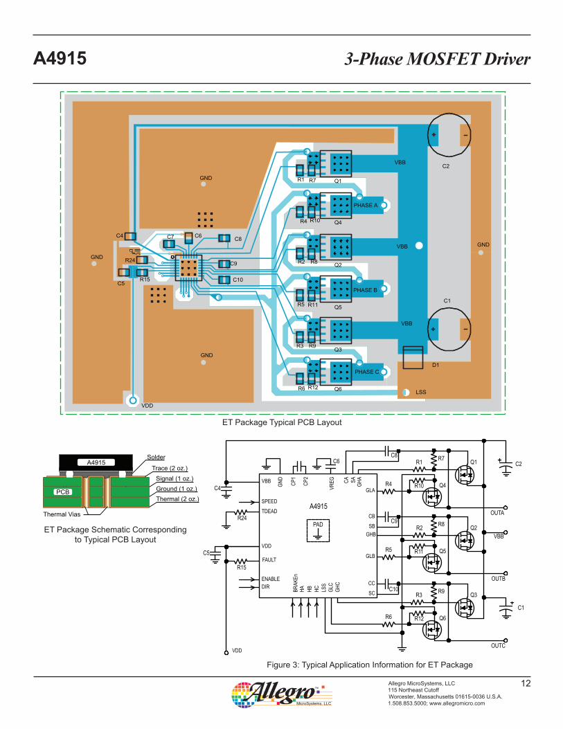
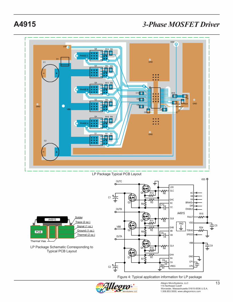
Layout RecommendationsCareful consideration must be given to PCB layout when design-ing high frequency, fast-switching, high-current circuits (refer to Figures 3 and 4):
• The A4915 ground, GND, and the high-current return of the ex-ternal MOSFETs should return separately to the negative side of
the motor supply filtering capacitor. This minimizes the effect of switching noise on the A4915.
• The exposed thermal pad should be connected to GND.• Minimize stray inductance by using short, wide copper traces
at the drain and source terminals of all power MOSFETs. This includes motor lead connections, the input power bus, and the common source of the low-side power MOSFETs. This mini-mizes voltages induced by fast switching of large load currents.
• Consider the use of small (100 nF) ceramic decoupling capaci-tors across the source and drain of the power MOSFETs, to limit fast transient voltage spikes caused by inductance in the traces.
• Keep the gate discharge return connections Sx and LSS as short as possible. Any inductance on these traces causes negative transitions on the corresponding A4915 terminals, which may exceed the Absolute Maximum Ratings. If this is likely, con-sider the use of clamping diodes to limit the negative excursion on these terminals with respect to GND.
• Supply decoupling for VBB, VREG, and VDD should be con-nected independently, close to the GND terminal. The decou-pling capacitors should also be connected as close as possible to the relevant supply terminal.
• Gate charge drive paths and gate discharge return paths may carry large transient current pulses. Therefore the traces from GHx, GLx, Sx (x = A, B, or C) and LSS should be as short as possible to reduce the inductance of the trace.
• Provide an independent connection from LSS to the common point of the power bridge. This can be the negative side of the motor supply filtering capacitor or one end of a sense resistor. It is not recommended to connect LSS directly to the GND termi-nal, as this may increase the noise at the digital inputs.
3-Phase MOSFET DriverA4915
12Allegro MicroSystems, LLC115 Northeast CutoffWorcester, Massachusetts 01615-0036 U.S.A.1.508.853.5000; www.allegromicro.com
R10 Q4R4
R8 Q2R2
R11 Q5R5
R9Q3
R3
R12 Q6R6
VBB
VBB
LSS
PHASE B
PHASE A
C7
VDD
C4
R24
R15C5
D1
C1
C2
GND
GND
GND
GND
PHASE C
C8C6
VBB
C9
C10
R7 Q1R1
ET Package Typical PCB Layout
Figure 3: Typical Application Information for ET Package
ET Package Schematic Corresponding to Typical PCB Layout
PCB
Thermal Vias
Trace (2 oz.)Signal (1 oz.)Ground (1 oz.)Thermal (2 oz.)
SolderA4915
BR
AK
En
HA
HB
HC
LS
S
GL
C
GH
C
CP
1
CA
SA
GH
A
CP
2
VR
EG
GN
D
C4
C5
R24
R15
A4915
DIR
ENABLE
FAULT
VDD
VDD
TDEAD
SPEED
VBB
PAD
Q5R5 R11
OUTB
C9
Q2R2R8
GLB
GHB
SB
CB
Q6R6 R12
OUTC
C10Q3R3
R9SC
CC
Q4R4 R10
OUTA
C8C6 Q1R1
R7
GLA
VBB
C1
C2
3-Phase MOSFET DriverA4915
13Allegro MicroSystems, LLC115 Northeast CutoffWorcester, Massachusetts 01615-0036 U.S.A.1.508.853.5000; www.allegromicro.com
PHASE C
C8
C6
C9
C10
R7Q1 R1
R10Q4 R4
R8Q2 R2
R11Q5 R5
R9Q3 R3
R12Q6 R6
VBB
LSS
PHASE B
PHASE A
C7
VDD
C4 R24
R15
C5
D1
C1
C2
GND
GND
GND
GND
LP Package Typical PCB Layout
LP Package Schematic Corresponding to Typical PCB Layout
PCB
Thermal Vias
Trace (2 oz.)Signal (1 oz.)Ground (1 oz.)Thermal (2 oz.)
SolderA4915
C4
C5R24
R15A4915
VREG
LSS
HC
BRAKEn
DIR
ENABLE
FAULT
VDD
VDD
TDEAD
SPEED
VBB
GND
CP1
CP2
HB
HA
PAD
Q5 R5R11
OUTB
C9
Q2 R2R8
GLB
GHB
SB
CB
Q6 R6R12
OUTC
C10Q3 R3
R9
GLC
GHC
SC
CC
Q4 R4R10
OUTA
C8
C6
Q1 R1R7
GLA
GHA
SA
CA
VBB
C1
C2
Figure 4: Typical application information for LP package

3-Phase MOSFET DriverA4915
14Allegro MicroSystems, LLC115 Northeast CutoffWorcester, Massachusetts 01615-0036 U.S.A.1.508.853.5000; www.allegromicro.com
Cx
18V
GHx
Sx
GLx
LSS
18V
18V
VREG
18V
18V
14V
VBB
18V
18V
14V
VDD
6V
VREG
18V
6V 6V
5 kΩ
VDD
SPEED
BRAKEDIR
ENABLE
2 kΩ
6V 6V 50 kΩ
VDD
HAHBHC
6V 6V
VDD VDD
2 kΩ
50 kΩ
CP1
18V
CP2FAULT
6V
Figure 5: Supplies Figure 6: Fault Output
Figure 7: Charge Pump Figure 8: Logic Inputs with Pull-down:BRAKEn, DIR, ENABLE
Figure 9: Hall inputs with pull-up:HA, HB, HC
Figure 11: Speed Input Figure 10: Gate Drive Outputs
Input / Output Structures
3-Phase MOSFET DriverA4915
15Allegro MicroSystems, LLC115 Northeast CutoffWorcester, Massachusetts 01615-0036 U.S.A.1.508.853.5000; www.allegromicro.com
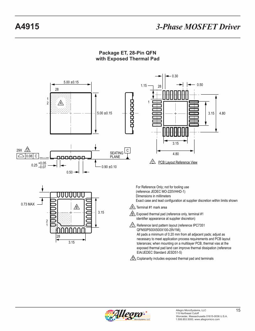
Package ET, 28-Pin QFNwith Exposed Thermal Pad
0.25 +0.05–0.07
0.500.90 ±0.10
C0.0829X
SEATINGPLANE
C
A Terminal #1 mark area
B Exposed thermal pad (reference only, terminal #1 identifier appearance at supplier discretion)
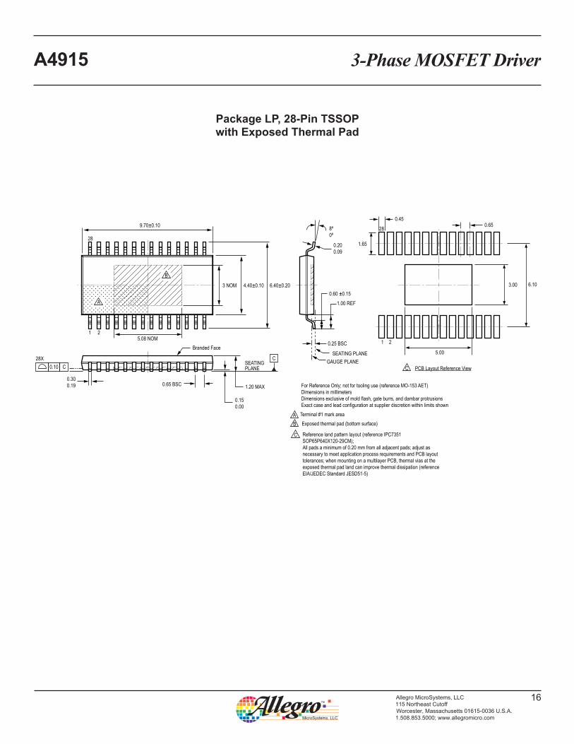
For Reference Only; not for tooling use(reference JEDEC MO-220VHHD-1)Dimensions in millimetersExact case and lead configuration at supplier discretion within limits shown
C Reference land pattern layout (reference IPC7351 QFN50P500X500X100-29V1M); All pads a minimum of 0.20 mm from all adjacent pads; adjust as necessary to meet application process requirements and PCB layout tolerances; when mounting on a multilayer PCB, thermal vias at the exposed thermal pad land can improve thermal dissipation (reference EIA/JEDEC Standard JESD51-5)
28
21
A
28
12
PCB Layout Reference View
B3.15
0.73 MAX
3.15
3.15
3.15
0.30
1
28 0.501.15
4.80
4.80
C
5.00 ±0.15
5.00 ±0.15
D
D Coplanarity includes exposed thermal pad and terminals
3-Phase MOSFET DriverA4915
16Allegro MicroSystems, LLC115 Northeast CutoffWorcester, Massachusetts 01615-0036 U.S.A.1.508.853.5000; www.allegromicro.com
Package LP, 28-Pin TSSOPwith Exposed Thermal Pad
A
1.20 MAX
0.150.00
0.300.19
0.200.09
8º0º
0.60 ±0.15
1.00 REF
CSEATINGPLANEC0.10
28X
0.65 BSC
0.25 BSC
21
28
9.70±0.10
4.40±0.10 6.40±0.20
GAUGE PLANESEATING PLANE
A Terminal #1 mark area
B
For Reference Only; not for tooling use (reference MO-153 AET)Dimensions in millimetersDimensions exclusive of mold flash, gate burrs, and dambar protrusions Exact case and lead configuration at supplier discretion within limits shown
B
Exposed thermal pad (bottom surface)
Branded Face5.08 NOM
3 NOM
C Reference land pattern layout (reference IPC7351 SOP65P640X120-29CM); All pads a minimum of 0.20 mm from all adjacent pads; adjust as necessary to meet application process requirements and PCB layout tolerances; when mounting on a multilayer PCB, thermal vias at the exposed thermal pad land can improve thermal dissipation (reference EIA/JEDEC Standard JESD51-5)
6.10
0.650.45
1.65
3.00
5.00
28
21
PCB Layout Reference ViewC
3-Phase MOSFET DriverA4915
17Allegro MicroSystems, LLC115 Northeast CutoffWorcester, Massachusetts 01615-0036 U.S.A.1.508.853.5000; www.allegromicro.com
Revision History
Revision Current Revision Date Description of Revision
1 April 1, 2013 Update EC table parameters
2 March 6, 2014 Update Absolute Maximum Ratings table and content on page 9
3 April 25, 2014 Revised Schematics on pp. 12 and 13
4 March 10, 2015 Changed Dead Time equation on page 9.
Copyright ©2012-2015, Allegro MicroSystems, LLCAllegro MicroSystems, LLC reserves the right to make, from time to time, such departures from the detail specifications as may be required to
permit improvements in the performance, reliability, or manufacturability of its products. Before placing an order, the user is cautioned to verify that the information being relied upon is current.
Allegro’s products are not to be used in any devices or systems, including but not limited to life support devices or systems, in which a failure of Allegro’s product can reasonably be expected to cause bodily harm.
The information included herein is believed to be accurate and reliable. However, Allegro MicroSystems, LLC assumes no responsibility for its use; nor for any infringement of patents or other rights of third parties which may result from its use.
For the latest version of this document, visit our website:www.allegromicro.com