Embed Size (px)
Citation preview
General DescriptionThe MAX1497/MAX1499 low-power, 3.5- and 4.5-digit,analog-to-digital converters (ADCs) with integrated light-emitting diode (LED) drivers operate from a single 2.7Vto 5.25V power supply. They include an internal refer-ence, a high-accuracy on-chip oscillator, and a multi-plexed LED display driver. An internal charge pumpgenerates the negative supply needed to power theintegrated input buffers for single-supply operation. TheADC is configurable for either a ±2V or ±200mV inputrange and it outputs its conversion results to an LEDand/or to a microcontroller (µC). Microcontroller communication is possible through an SPI™-/QSPI™-/MICROWIRE™-compatible serial interface. TheMAX1497 is a 3.5-digit (±1999 count) device and theMAX1499 is a 4.5-digit (±19,999 count) device.
The MAX1497/MAX1499 do not require external preci-sion integrating capacitors, autozero capacitors, crystaloscillators, charge pumps, or other circuitry requiredwith dual-slope ADCs (commonly used in panel metercircuits).
These devices also feature on-chip buffers for the dif-ferential signal and reference inputs, allowing directinterface with high-impedance signal sources. In addi-tion, they use continuous internal offset-calibration andoffer >100dB rejection of 50Hz and 60Hz line noise.Other features include data hold and peak detection,overrange and underrange detection, and a user-pro-grammable low-battery monitor.
The MAX1499 is available in a 32-pin, 7mm 7mmTQFP package and the MAX1497 is available in 28-pinSSOP and 28-pin PDIP packages. All devices in thisfamily operate over the -40°C to +85°C extended tem-perature range.
ApplicationsDigital Panel Meters
Hand-Held Meters
Digital Voltmeters
Digital Multimeters
Features♦ High Resolution
MAX1499: 4.5 Digits (±19,999 Count) MAX1497: 3.5 Digits (±1999 Count)
♦ Sigma-Delta ADC ArchitectureNo Integrating Capacitors RequiredNo Autozeroing Capacitors Required>100dB of Simultaneous 50Hz and 60HzRejection
♦ Operate from a Single 2.7V or 5.25V Supply
♦ Selectable Input Range of ±200mV or ±2V
♦ Selectable Voltage Reference: Internal 2.048V orExternal
♦ Internal High-Accuracy Oscillator Needs NoExternal Components
♦ Automatic Offset Calibration
♦ Low Power (Exclude LED Driver Current)Maximum 664µA Operating CurrentMaximum 268µA Shutdown Current
♦ Small 32-Pin, 7mm x 7mm TQFP Package (4.5Digits), 28-Pin SSOP Package (3.5 Digits)
♦ Also Available in a PDIP Package (3.5 Digits)
♦ Multiplexed LED DriversResistor-Programmable Segment Current
♦ SPI-/QSPI-/MICROWIRE-Compatible SerialInterface
♦ Extended Temperature Range (-40°C to +85°C)
MA
X1
49
7/M
AX
14
99
3.5- and 4.5-Digit, Single-Chip ADCs with LEDDrivers and µC Interface
________________________________________________________________ Maxim Integrated Products 1
Ordering Information
19-3054; Rev 1a; 2/04
For pricing, delivery, and ordering information, please contact Maxim/Dallas Direct! at 1-888-629-4642, or visit Maxim’s website at www.maxim-ic.com.
PART TEMP RANGEPIN-PACKAGE
RESOLUTION(DIGITS)
MAX1497EAI* -40°C to +85°C 28 SSOP 3.5
MAX1497EPI -40°C to +85°C 28 PDIP 3.5
MAX1499ECJ -40°C to +85°C 32 TQFP 4.5
Pin Configurations appear at end of data sheet.
*Future product—contact factory for availability.
SPI/QSPI are trademarks of Motorola, Inc.MICROWIRE is a trademark of National Semiconductor Corp.

MA
X1
49
7/M
AX
14
99
3.5- and 4.5-Digit, Single-Chip ADCs with LEDDrivers and µC Interface
2 _______________________________________________________________________________________
ABSOLUTE MAXIMUM RATINGS
Stresses beyond those listed under “Absolute Maximum Ratings” may cause permanent damage to the device. These are stress ratings only, and functionaloperation of the device at these or any other conditions beyond those indicated in the operational sections of the specifications is not implied. Exposure toabsolute maximum rating conditions for extended periods may affect device reliability.
AVDD to GND (MAX1499).........................................-0.3V to +6VDVDD to GND (MAX1499) ........................................-0.3V to +6VAIN+, AIN- to GND (MAX1499) ...........VNEG to (AVDD to +0.3V)REF+, REF- to GND (MAX1499) ......... VNEG to (AVDD to +0.3V)LOWBATT to GND (MAX1499) ................-0.3V to (AVDD + 0.3V)CLK, EOC, CS, DIN, SCLK, DOUT to GND (MAX1499) .......................-0.3V to (DVDD + 0.3V)VNEG to GND (MAX1499) .......................-2.6V to (AVDD + 0.3V)LED_EN to GND (MAX1499)....................-0.3V to (DVDD + 0.3V)ISET to GND (MAX1499)..........................-0.3V to (AVDD + 0.3V)VDD to GND (MAX1497) ...........................................-0.3V to +6VAIN+, AIN- to GND (MAX1497)..............VNEG to (VDD to +0.3V)REF+, REF- to GND (MAX1497) ........... VNEG to (VDD to +0.3V)CLK, EOC, CS, DIN, SCLK, DOUT to GND (MAX1497)..........................-0.3V to (VDD + 0.3V)VNEG to GND (MAX1497)..........................-2.6V to (VDD + 0.3V)ISET to GND (MAX1497) ............................-0.3V to (VDD + 0.3V)
VLED to GLED..........................................................-0.3V to +6VGLED to GND........................................................-0.3V to +0.3VSEG_ to GLED..........................................-0.3V to (VLED + 0.3V)DIG_ to GLED ..........................................-0.3V to (VLED + 0.3V)DIG_ Sink Current .............................................................300mADIG_ Source Current...........................................................50mASEG_ Sink Current ..............................................................50mASEG_ Source Current..........................................................50mAMaximum Current Input into Any Other Pin ........................50mAContinuous Power Dissipation (TA = +70°C)
32-Pin TQFP (derate 20.7mW/°C above +70°C).....1652.9mW28-Pin SSOP (derate 9.5mW/°C above +70°C) ...........762mW28-Pin PDIP (derate 14.3mW/°C above +70°C)......1142.9mW
Operating Temperature Range ...........................-40°C to +85°CJunction Temperature ......................................................+150°CStorage Temperature Range .............................-60°C to +150°CLead Temperature (soldering, 10s) .................................+300°C
ELECTRICAL CHARACTERISTICS(AVDD = DVDD = VDD = +2.7V to +5.25V, GND = 0, GLED = 0, VLED = +2.7V to +5.25V, VREF+ - VREF- = 2.048V (external reference)CREF+ = CREF- = 0.1µF, CVNEG = 0.1µF. Internal clock mode, unless otherwise noted. All specifications are at TA = TMIN to TMAX.Typical values are at TA = +25°C, unless otherwise noted.)
PARAMETER SYMBOL CONDITIONS MIN TYP MAX UNITS
DC ACCURACY
MAX1499 -19,999 +19,999Noise-Free Resolution
MAX1497 -1999 +1999Count
2.000V range ±1Integral Nonlinearity (Note 1) INL
200mV range ±1Count
Range Change Ratio(VAIN+ - VAIN- = 0.100V) on 200mV range(VAIN+ - VAIN- = 0.100V) on 2.0V range
10:1 Ratio
Rollover ErrorVAIN+ - VAIN- = full scaleVAIN- - VAIN+ = full scale
±1 Count
Output Noise 10 µVP-P
Offset Error (Zero Input Reading) Offset VIN = 0 (Note 2) -0 0 Reading
Gain Error (Note 3) -0.5 +0.5 %FSR
Offset Drift (Zero Reading Drift) VIN = 0 (Note 4) 0.1 µV/°C
Gain Drift ±1 ppm/°C
INPUT CONVERSION RATE
External-Clock Frequency 4.9152 MHz
External-Clock Duty Cycle 40 60 %
Internal clock 5Conversion Rate
External clock, fCLK = 4.9152MHz 5Hz

MA
X1
49
7/M
AX
14
99
3.5- and 4.5-Digit, Single-Chip ADCs with LEDDrivers and µC Interface
_______________________________________________________________________________________ 3
PARAMETER SYMBOL CONDITIONS MIN TYP MAX UNITS
ANALOG INPUTS (AIN+, AIN-) (bypass to GND with 0.1µF or greater capacitors)
RANGE bit = 0 -2.0 +2.0AIN Input Voltage Range (Note 5)
RANGE bit = 1 -0.2 +0.2
AIN Absolute Input VoltageRange to GND
-2.2 +2.2
V
Internal clock mode, 50Hz and 60Hz ±2% 100Normal-Mode 50Hz and 60HzRejection (Simultaneously) External clock mode, 50Hz and 60Hz ±2%,
fCLK = 4.9152MHz120
dB
Common-Mode 50Hz and 60HzRejection (Simultaneously)
CMR For 50Hz and 60Hz ±2%, RSOURCE < 10kΩ 150 dB
Common-Mode Rejection CMR At DC 100 dB
Input Leakage Current 10 nA
Input Capacitance 10 pF
Average Dynamic Input Current (Note 6) -20 +20 nA
LOW-BATTERY VOLTAGE MONITOR (LOWBATT) (MAX1499 only)
LOWBATT TripThreshold 2.048 V
LOWBATT Leakage Current 10 pA
Hysteresis 20 mV
INTERNAL REFERENCE (REF- = GND, INTREF bit = 1) (bypass REF+ to GND with a 4.7µF capacitor)
REF Output Voltage VREF AVDD = VDD = 5V 2.007 2.048 2.089 V
REF Output Short-Circuit Current 1 mA
REF Output TemperatureCoefficient
TCVREF AVDD = VDD = 5V 40 ppm/°C
Load Regulation ISOURCE = 0 to 300µA, ISINK = 0 to 30µA 6 mV/µA
Line Regulation 50 µV/V
0.1Hz to 10Hz 25Noise Voltage
10Hz to 10kHz 400µVP-P
EXTERNAL REFERENCE (INTREF bit = 0) (bypass REF+ and REF- to GND with 0.1µF or greater capacitors)
REF Input Voltage Differential (VREF+ - VREF-) 2.048
Absolute REF+, REF- InputVoltage to GND
-2.2 +2.2V
Internal clock mode, 50Hz and 60Hz ±2% 100Normal-Mode 50Hz and 60HzRejection (Simultaneously) External clock mode, 50Hz and 60Hz ±2%,
fCLK = 4.9152MHz120
dB
Common-Mode 50Hz and 60HzRejection (Simultaneously)
CMR For 50Hz and 60Hz ±2%, RSOURCE < 10kΩ 150 dB
Common-Mode Rejection CMR At DC 100 dB
Input Leakage Current 10 nA
ELECTRICAL CHARACTERISTICS (continued)(AVDD = DVDD = VDD = +2.7V to +5.25V, GND = 0, GLED = 0, VLED = +2.7V to +5.25V, VREF+ - VREF- = 2.048V (external reference)CREF+ = CREF- = 0.1µF, CVNEG = 0.1µF. Internal clock mode, unless otherwise noted. All specifications are at TA = TMIN to TMAX.Typical values are at TA = +25°C, unless otherwise noted.)

MA
X1
49
7/M
AX
14
99
3.5- and 4.5-Digit, Single-Chip ADCs with LEDDrivers and µC Interface
4 _______________________________________________________________________________________
PARAMETER SYMBOL CONDITIONS MIN TYP MAX UNITS
Input Capacitance 10 pF
Average Dynamic Input Current (Note 6) -20 +20 nA
CHARGE PUMP
Output Voltage VNEG CVNEG = 0.1µF -2.60 -2.42 -2.30 V
DIGITAL INPUTS (SCLK, DIN, CS, CLK)
Input Current IIN VIN = 0 or DVDD = VDD -10 +10 µA
MAX14990.3 xDVDD
Input Low Voltage VINL
MAX14970.3 xVDD
V
MAX14990.7 xDVDD
Input High Voltage VINH
MAX14970.7 xVDD
V
Input Hysteresis VHYS DVDD = VDD = 3.0V 200 mV
DIGITAL OUTPUTS (DOUT, EOC)
Output Low Voltage VOL ISINK = 1mA 0.4 V
ISOURCE = 200µA, M AX 14990.8 xDVDD
Output High Voltage VOH
ISOURCE = 200µA, M AX 14970.8 xVDD
V
Tri-State Leakage Current IL DOUT only -1 +1 µA
Tri-State Output Capacitance COUT DOUT only 15 pF
POWER SUPPLY (Note 10)
VDD Voltage VDD MAX1497 2.70 5.25 V
AVDD Voltage AVDD MAX1499 2.70 5.25 V
DVDD Voltage DVDD MAX1499 2.70 5.25 V
Power-Supply Rejection VDD PSRR (Note 7) 80 dB
Power-Supply Rejection AVDD PSRRA (Note 7) 80 dB
Power-Supply Rejection DVDD PSRRD (Note 7) 100 dB
VDD = 5.25V 664 744
VDD = 3.3V 618 663VDD Current (Notes 8, 9) IVDD
Standby mode 268 325
µA
AVDD = 5.25V 640
AVDD = 3.3V 600AVDD Current (Notes 8, 9) IAVDD
Standby mode 305
µA
ELECTRICAL CHARACTERISTICS (continued)(AVDD = DVDD = VDD = +2.7V to +5.25V, GND = 0, GLED = 0, VLED = +2.7V to +5.25V, VREF+ - VREF- = 2.048V (external reference)CREF+ = CREF- = 0.1µF, CVNEG = 0.1µF. Internal clock mode, unless otherwise noted. All specifications are at TA = TMIN to TMAX.Typical values are at TA = +25°C, unless otherwise noted.)

MA
X1
49
7/M
AX
14
99
3.5- and 4.5-Digit, Single-Chip ADCs with LEDDrivers and µC Interface
_______________________________________________________________________________________ 5
PARAMETER SYMBOL CONDITIONS MIN TYP MAX UNITS
DVDD = 5V 320
DVDD = 3.3V 180DVDD Current (Notes 8, 9) IDVDD
Standby mode 20
µA
LED Drivers Bias Current From AVDD or VDD 120 µA
LED DRIVERS (Table 6)
LED Supply Voltage VLED 2.70 5.25 V
LED Shutdown Supply Current ISHDN LED driver shutdown mode 10 µA
LED Supply Current ILEDSeven segments and decimal point on,RISET = 25kΩ
176 mA
MAX1499 512Display Scan Rate fOSC
MAX1497 640Hz
Segment Current Slew Rate ∆ISEG/∆t 25 mA/µs
DIG_ Voltage Low VDIG IDIG_ = 176mA 0.178 0.300 V
Segment Drive Source CurrentMatching
∆ISEG ±3 ±10 %
Segment Drive Source Current ISEG VLED - VSEG = 0.6V, RISET = 25kΩ 16 20 25.5 mA
Interdigit Blanking Time 4 µs
ELECTRICAL CHARACTERISTICS (continued)(AVDD = DVDD = VDD = +2.7V to +5.25V, GND = 0, GLED = 0, VLED = +2.7V to +5.25V, VREF+ - VREF- = 2.048V (external reference)CREF+ = CREF- = 0.1µF, CVNEG = 0.1µF. Internal clock mode, unless otherwise noted. All specifications are at TA = TMIN to TMAX.Typical values are at TA = +25°C, unless otherwise noted.)

MA
X1
49
7/M
AX
14
99
3.5- and 4.5-Digit, Single-Chip ADCs with LEDDrivers and µC Interface
6 _______________________________________________________________________________________
TIMING CHARACTERISTICS (Notes 11, 12, Figure 8)(AVDD = DVDD = VDD = +2.7V to +5.25V, GND = 0, GLED = 0, VLED = +2.7V to +5.25V, VREF+ - VREF- = 2.048V (external reference)CREF+ = CREF- = 0.1µF, CVNEG = 0.1µF. Internal clock mode, unless otherwise noted. All specifications are at TA = TMIN to TMAX.Typical values are at TA = +25°C, unless otherwise noted.)
PARAMETER SYMBOL CONDITIONS MIN TYP MAX UNITS
SCLK Operating Frequency fSCLK 0 4.2 MHz
SCLK Pulse-Width High tCH 100 ns
SCLK Pulse-Width Low tCL 100 ns
DIN to SCLK Setup tDS 50 ns
DIN to SCLK Hold tDH 0 ns
CS Fall to SCLK Rise Setup tCSS 50 ns
SCLK Rise to CS Rise Hold tCSH 0 ns
SCLK Fall to DOUT Valid tDO CLOAD = 50pF, Figures 13, 14 120 ns
CS Rise to DOUT Disable tTR CLOAD = 50pF, Figures 13, 14 120 ns
CS Fall to DOUT Enable tDV CLOAD = 50pF, Figures 13, 14 120 ns
Note 1: Integral nonlinearity is the deviation of the analog value at any code from its theoretical value after nulling the gain error andoffset error.
Note 2: Offset calibrated. See OFFSET_CAL1 and OFFSET_CAL2 (MAX1499 only) in the On-Chip Registers section.Note 3: Offset nulled.Note 4: Offset drift error is eliminated by recalibration at the new temperature.Note 5: The input voltage range for the analog inputs is given with respect to the voltage on the negative input of the differential pair.Note 6: VAIN+ or VAIN- = -2.2V to +2.2V. VREF+ or VREF- = -2.2V to +2.2V. All input structures are identical. Production tested on
AIN+ and REF+ only.Note 7: Measured at DC by changing the power-supply voltage from 2.7V to 5.25V and measuring the effect on the conversion
error with external reference. PSRR at 50Hz and 60Hz exceeds 120dB with filter notches at 50Hz and 60Hz (Figure 2).Note 8: CLK and SCLK are disabled.Note 9: LED drivers are disabled.Note 10: Power-supply currents are measured with all digital inputs at either GND, DVDD, or VDD and with the device in internal-clock mode.Note 11: All input signals are specified with tRISE = tFALL = 5ns (10% to 90% of DVDD) and are timed from a voltage level of 50% of
DVDD, unless otherwise noted.Note 12: See the serial-interface timing diagrams.

MA
X1
49
7/M
AX
14
99
3.5- and 4.5-Digit, Single-Chip ADCs with LEDDrivers and µC Interface
_______________________________________________________________________________________ 7
Typical Operating Characteristics(AVDD = DVDD = VDD = +2.7V to +5.25V, VLED = +2.7V to +5.25V, GND = 0, GLED = 0, external reference mode, REF+ = 2.048V,REF- = GND, CREF+ = CREF- = 0.1µF, RANGE bit = 1, internal clock mode, CVNEG = 0.1µF. TA = +25°C, unless otherwise noted.)
SUPPLY CURRENTvs. SUPPLY VOLTAGE (MAX1499)
MAX
1497
/99
toc0
1
SUPPLY VOLTAGE (V)
SUPP
LY C
URRE
NT (µ
A)
4.754.253.753.25
100
200
300
400
500
600
700
02.75 5.25
ANALOG SUPPLY
DIGITAL SUPPLY
SUPPLY CURRENTvs. SUPPLY VOLTAGE (MAX1497)
MAX
1497
/99
toc0
2
SUPPLY VOLTAGE (V)
SUPP
LY C
URRE
NT (µ
A)
4.744.233.723.21
450
500
550
600
650
700
4002.70 5.25
SUPPLY CURRENTvs. TEMPERATURE (MAX1499)
MAX
1497
/99
toc0
3
TEMPERATURE (°C)
SUPP
LY C
URRE
NT (µ
A)
605040302010
100
200
300
400
500
600
700
00 70
ANALOG SUPPLY
DIGITAL SUPPLY
SUPPLY CURRENTvs. TEMPERATURE (MAX1497)
MAX
1497
/99
toc0
4
TEMPERATURE (°C)
SUPP
LY C
URRE
NT (µ
A)
6035-15 10
610
640
630
620
650
660
670
680
690
700
600-40 85
SHUTDOWN CURRENTvs. TEMPERATURE (MAX1499)
MAX
1497
/99
toc0
5
TEMPERATURE (°C)
SHUT
DOW
N CU
RREN
T (µ
A)
605040302010
50
100
150
200
250
300
00 70
ANALOG SUPPLY
DIGITAL SUPPLY
SHUTDOWN CURRENTvs. SUPPLY VOLTAGE (MAX1499)
MAX
1497
/99
toc0
7
SUPPLY VOLTAGE (V)
SHUT
DOW
N CU
RREN
T (µ
A)
4.754.253.753.25
50
100
150
200
250
300
02.75 5.25
ANALOG SUPPLY
DIGITAL SUPPLY
SHUTDOWN CURRENTvs. SUPPLY VOLTAGE (MAX1497)
MAX
1497
/99
toc0
8
SUPPLY VOLTAGE (V)
SHUT
DOW
N CU
RREN
T (µ
A)
4.744.233.723.21
50
150
100
200
250
300
350
02.70 5.25
MAX1499OFFSET ERROR vs. SUPPLY VOLTAGE
MAX
1497
/99
toc0
9
SUPPLY VOLTAGE (V)
OFFS
ET E
RROR
(LSB
)
4.754.253.753.25
-0.11
-0.06
-0.01
0.04
0.09
0.14
0.19
-0.162.75 5.25
SHUTDOWN CURRENTvs. TEMPERATURE (MAX1497)
MAX
1497
/99
toc0
6
TEMPERATURE (°C)
SHUT
DOW
N CU
RREN
T (µ
A)
6035-15 10
50
150
100
200
250
300
350
0-40 85

INTERNAL REFERENCE VOLTAGEvs. TEMPERATURE
MAX
1497
/99
toc1
6
TEMPERATURE (°C)
REFE
RENC
E VO
LTAG
E (V
)
605040302010
2.046
2.045
2.047
2.049
2.048
2.051
2.050
2.053
2.052
2.054
2.0440 70
INTERNAL REFERENCE VOLTAGEvs. ANALOG SUPPLY VOLTAGE
MAX
1497
/99
toc1
7
SUPPLY VOLTAGE (V)
REFE
RENC
E VO
LTAG
E (V
)
4.754.253.753.25
2.045
2.046
2.047
2.048
2.049
2.050
2.0442.75 5.25
MA
X1
49
7/M
AX
14
99
3.5- and 4.5-Digit, Single-Chip ADCs with LEDDrivers and µC Interface
8 _______________________________________________________________________________________
Typical Operating Characteristics (continued)(AVDD = DVDD = VDD = +2.7V to +5.25V, VLED = +2.7V to +5.25V, GND = 0, GLED = 0, external reference mode, REF+ = 2.048V,REF- = GND, CREF+ = CREF- = 0.1µF, RANGE bit = 1, internal clock mode, CVNEG = 0.1µF. TA = +25°C, unless otherwise noted.)
MAX1499OFFSET ERROR vs. TEMPERATURE
MAX
1497
/99
toc1
0
TEMPERATURE (°C)
OFFS
ET E
RROR
(LSB
)
605010 20 30 40
-0.1
0
0.1
0.2
0.3
0.4
0.5
0.6
-0.20 70
MAX1499GAIN ERROR vs. SUPPLY VOLTAGE
MAX
1497
/99
toc1
1
SUPPLY VOLTAGE (V)
GAIN
ERR
OR (%
FUL
L SC
ALE)
4.754.253.25 3.75
-0.08
-0.04
-0.06
-0.02
0
0.02
0.04
0.06
0.08
-0.102.75 5.25
MAX1499GAIN ERROR vs. TEMPERATURE
MAX
1497
/99
toc1
2
TEMPERATURE (°C)
GAIN
ERR
OR (%
FUL
L SC
ALE)
605030 402010
-0.09
-0.08
-0.07
-0.06
-0.05
-0.04
-0.03
-0.02
-0.01
0
-0.100 70
MAX1499(±200mV INPUT RANGE) INL vs. OUTPUT CODE
MAX
1497
/99
toc1
3
OUTPUT CODE
INL
(COU
NTS)
10,0000-10,000
-0.5
0
0.5
1.0
-1.0-20,000 20,000
MAX1499(±2V INPUT RANGE) INL vs. OUTPUT CODE
MAX
1497
/99
toc1
4
OUTPUT CODE
INL
(COU
NTS)
10,0000-10,000
-0.5
0
0.5
1.0
-1.0-20,000 20,000
NOISE DISTRIBUTION
MAX
1497
/99
toc1
5
NOISE (LSB)
PERC
ENTA
GE O
F UN
ITS
(%)
0.80.70.60.50.40.30.20.10-0.1
5
10
15
20
25
0-0.2
DATA OUTPUT RATEvs. TEMPERATURE
MAX
1497
/99
toc1
8
TEMPERATURE (°C)
DATA
OUT
PUT
RATE
(Hz)
6035-15 10
4.92
4.98
4.96
4.94
5.00
5.02
5.04
5.06
5.08
5.10
4.90-40 85

MA
X1
49
7/M
AX
14
99
3.5- and 4.5-Digit, Single-Chip ADCs with LEDDrivers and µC Interface
_______________________________________________________________________________________ 9
Typical Operating Characteristics (continued)(AVDD = DVDD = VDD = +2.7V to +5.25V, VLED = +2.7V to +5.25V, GND = 0, GLED = 0, external reference mode, REF+ = 2.048V,REF- = GND, CREF+ = CREF- = 0.1µF, RANGE bit = 1, internal clock mode, CVNEG = 0.1µF. TA = +25°C, unless otherwise noted.)
DATA OUTPUT RATEvs. SUPPLY VOLTAGE
MAX
1497
/99
toc1
9
SUPPLY VOLTAGE (V)
DATA
OUT
PUT
RATE
(Hz)
4.744.233.21 3.72
4.995
4.990
4.985
5.000
5.005
5.010
5.015
5.020
4.9802.70 5.25
OFFSET ERRORvs. COMMON-MODE VOLTAGE
MAX
1497
/99
toc2
0
COMMON-MODE VOLTAGE (V)
OFFS
ET E
RROR
(LSB
)
1.51.0-1.5 -1.0 -0.5 0 0.5
-0.15
-0.10
-0.05
0
0.05
0.10
0.15
0.20
-0.20-2.0 2.0
SEGMENT CURRENTvs. SUPPLY VOLTAGE
MAX
1497
/99
toc2
3
SUPPLY VOLTAGE (V)
SEGM
ENT
CURR
ENT
(µA)
4.744.233.723.21
5
10
15
20
25
30
02.70 5.25
RISET = 25kΩ
VNEG STARTUP SCOPE SHOT
MAX
1497
/99
toc2
1
20ms/div
2V/div
1V/div
VDD
VNEG
CHARGE-PUMP OUTPUT VOLTAGEvs. ANALOG SUPPLY VOLTAGE
MAX
1497
/99
toc2
2
SUPPLY VOLTAGE (V)
V NEG
VOL
TAGE
(V)
4.754.253.753.25
-2.48
-2.46
-2.44
-2.42
-2.40
-2.502.75 5.25
MA
X1
49
7/M
AX
14
99
3.5- and 4.5-Digit, Single-Chip ADCs with LEDDrivers and µC Interface
10 ______________________________________________________________________________________
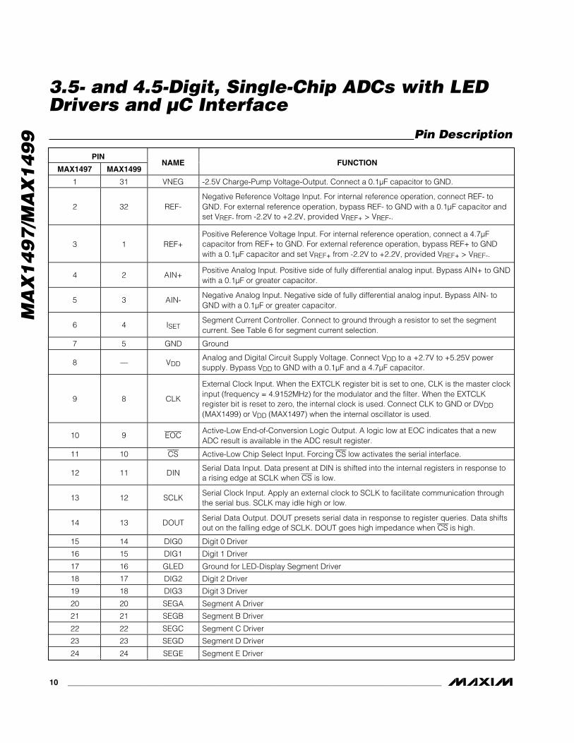
Pin Description
PIN
MAX1497 MAX1499NAME FUNCTION
1 31 VNEG -2.5V Charge-Pump Voltage-Output. Connect a 0.1µF capacitor to GND.
2 32 REF-Negative Reference Voltage Input. For internal reference operation, connect REF- toGND. For external reference operation, bypass REF- to GND with a 0.1µF capacitor andset VREF- from -2.2V to +2.2V, provided VREF+ > VREF-.
3 1 REF+Positive Reference Voltage Input. For internal reference operation, connect a 4.7µFcapacitor from REF+ to GND. For external reference operation, bypass REF+ to GNDwith a 0.1µF capacitor and set VREF+ from -2.2V to +2.2V, provided VREF+ > VREF-.
4 2 AIN+Positive Analog Input. Positive side of fully differential analog input. Bypass AIN+ to GNDwith a 0.1µF or greater capacitor.
5 3 AIN-Negative Analog Input. Negative side of fully differential analog input. Bypass AIN- toGND with a 0.1µF or greater capacitor.
6 4 ISETSegment Current Controller. Connect to ground through a resistor to set the segmentcurrent. See Table 6 for segment current selection.
7 5 GND Ground
8 — VDDAnalog and Digital Circuit Supply Voltage. Connect VDD to a +2.7V to +5.25V powersupply. Bypass VDD to GND with a 0.1µF and a 4.7µF capacitor.
9 8 CLK
External Clock Input. When the EXTCLK register bit is set to one, CLK is the master clockinput (frequency = 4.9152MHz) for the modulator and the filter. When the EXTCLKregister bit is reset to zero, the internal clock is used. Connect CLK to GND or DVDD(MAX1499) or VDD (MAX1497) when the internal oscillator is used.
10 9 EOCActive-Low End-of-Conversion Logic Output. A logic low at EOC indicates that a newADC result is available in the ADC result register.
11 10 CS Active-Low Chip Select Input. Forcing CS low activates the serial interface.
12 11 DINSerial Data Input. Data present at DIN is shifted into the internal registers in response toa rising edge at SCLK when CS is low.
13 12 SCLKSerial Clock Input. Apply an external clock to SCLK to facilitate communication throughthe serial bus. SCLK may idle high or low.
14 13 DOUTSerial Data Output. DOUT presets serial data in response to register queries. Data shiftsout on the falling edge of SCLK. DOUT goes high impedance when CS is high.
15 14 DIG0 Digit 0 Driver
16 15 DIG1 Digit 1 Driver
17 16 GLED Ground for LED-Display Segment Driver
18 17 DIG2 Digit 2 Driver
19 18 DIG3 Digit 3 Driver
20 20 SEGA Segment A Driver
21 21 SEGB Segment B Driver
22 22 SEGC Segment C Driver
23 23 SEGD Segment D Driver
24 24 SEGE Segment E Driver

MA
X1
49
7/M
AX
14
99
3.5- and 4.5-Digit, Single-Chip ADCs with LEDDrivers and µC Interface
______________________________________________________________________________________ 11
Detailed DescriptionThe MAX1497/MAX1499 low-power, highly integratedADCs with LED drivers convert a ±2V differential inputvoltage (one count is equal to 100µV for the MAX1499and 1mV for the MAX1497) with a sigma-delta ADC andoutput the result to an LED or µC. An additional±200mV input range (one count is equal to 10µV for theMAX1499 and 100µV for the MAX1497) is available tomeasure small signals with increased resolution.
The devices operate from a single 2.7V to 5.25V powersupply and offer 3.5-digit (MAX1497) or 4.5-digit(MAX1499) conversion results. An internal 2.048V refer-ence, internal charge pump, and a high-accuracy on-chip oscillator eliminate external components.
The MAX1497/MAX1499 interface with a µC using anSPI-/QSPI-/MICROWIRE-compatible serial interface.Data can either be sent directly to the display or to theµC first for processing before being displayed.
The devices also feature on-chip buffers for the differ-ential input signal and external reference inputs, allow-ing direct interface with high-impedance signalsources. In addition, they use continuous internal offset-calibration and offer >100dB of 50Hz and 60Hz linenoise rejection. Other features include data hold andpeak detection, overrange and underrange detection.The MAX1499 also provides a low-battery monitor.
Analog Input ProtectionInternal protection diodes limit the analog input rangefrom VNEG to (AVDD + 0.3V) for the MAX1499, andfrom VNEG to (VDD to 0.3V) for the MAX1497. If theanalog input exceeds this range, limit the input currentto 10mA.
Internal Analog Input/Reference BuffersThe MAX1497/MAX1499 analog input/reference buffersallow the use of high-impedance signal sources. Theinput buffers’ common-mode input range allows the ana-log inputs and the reference to range from -2.2V to +2.2V.
ModulatorThe MAX1497/MAX1499 perform analog-to-digital con-versions using a single-bit, 3rd-order, sigma-delta mod-ulator. The sigma-delta modulator converts the inputsignal into a digital pulse train whose average dutycycle represents the digitized signal information. Themodulator quantizes the input signal at a much highersample rate than the bandwidth of the input.
The MAX1497/MAX1499 modulator provides 3rd-orderfrequency shaping of the quantization noise resultingfrom the single-bit quantizer. The modulator is fully dif-ferential for maximum signal-to-noise ratio and mini-mum susceptibility to power-supply noise. A single-bitdata stream is then presented to the digital filter toremove the frequency-shaped quantization noise.
Pin Description (continued)
PIN
MAX1497 MAX1499NAME FUNCTION
25 25 VLEDLED-Display Segment-Driver Supply. Connect to a +2.7V to +5.25V supply. Bypass witha 0.1µF capacitor to GLED.
26 26 SEGF Segment F Driver
27 27 SEGG Segment G Driver
28 28 SEGDP Segment DP Driver
— 6 AVDDAnalog Positive Supply Voltage. Connect AVDD to a +2.7V to +5.25V power supply.Bypass AVDD to GND with a 0.1µF capacitor.
— 7 DVDDDigital Positive Supply Voltage. Connect DVDD to a +2.7V to +5.25V power supply.Bypass DVDD to GND with a 0.1µF capacitor.
— 19 DIG4 Digit 4 Driver
— 29 LED_ENActive-High LED Enable. The MAX1499 LED display driver turns off when LED_EN isdriven to logic low. The MAX1499 LED display driver turns on when LED_EN is driven tologic high.
— 30 LOWBATTLow-Battery Voltage Monitor. When the LOWBATT input voltage is lower than 2.048V, theLOWBATT bit in the status register is set to one.

MA
X1
49
7/M
AX
14
99
3.5- and 4.5-Digit, Single-Chip ADCs with LEDDrivers and µC Interface
12 ______________________________________________________________________________________
Digital FilteringThe MAX1497/MAX1499 contain an on-chip digital low-pass filter that processes the data stream from themodulator using a SINC4 response:
The SINC4 filter has a settling time of four output dataperiods (4 x 200ms).
The MAX1497/MAX1499 have 25% overrange capabili-ty built into the modulator and digital filter. The digital fil-ter is optimized for the fCLK equal to 4.9152MHz. Otherclock frequencies can be used; however, 50Hz/60Hznoise rejection decreases. The frequency response of theSINC4 filter is calculated as follows:
where N is the oversampling ratio, and fm = N x outputdata rate = 5Hz.
Filter CharacteristicsFigure 2 shows the filter frequency response. TheSINC4 characteristic -3dB cutoff frequency is 0.228times the first notch frequency (5Hz). The oversamplingratio (OSR) for the MAX1497 is 128 and the OSR for theMAX1499 is 1024.
The output data rate for the digital filter corresponds tothe positioning of the first notch of the filter’s frequencyresponse. The notches of the SINC4 filter are repeatedat multiples of the first notch frequency. The SINC4 filterprovides an attenuation of better than 100dB at thesenotches. For example, 50Hz is equal to 10 times thefirst notch frequency and 60Hz is equal to 12 times thefirst notch frequency.
For large step changes at the input, allow a settlingtime of 800ms before valid data is read.
Clock ModesConfigure the MAX1497/MAX1499 to use either theinternal oscillator or an externally applied clock to drivethe modulator and filter. Set the EXTCLK bit in the con-trol register to zero to put the device in internal-clockmode. Set the EXTCLK bit to one to put the device in
H zN
Z
Z
H fN
Nf
f
ff
N
m
m
( )( )
( )
( )
sin
sin
=
=
1 1
1
1
1
4
4
-
-
-
-
π
π
sin( )xx
4
MAX1499
BINARY-TO-BCD
CONVERTERSADC
LEDDRIVER
INPUTBUFFERS
-2.5V
AIN+
AIN-
REF+
REF-
+2.5V
AVDD DVDD
GLED
2.048VBANDGAP
REFERENCE
OSCILLATORCLOCK
SCLK DIN DOUT
EOC
SEG1
SEGFSEGDPDIG0
DIG4
CLK
CS
SERIAL I/O AND CONTROL
+2.5V
2.048V
GND
A = 1.22
TOCONTROL
CHARGEPUMP
-2.5V
LOWBATTVNEG
LED_EN
VLEDISET
Figure 1. MAX1499 Functional Diagram

MA
X1
49
7/M
AX
14
99
3.5- and 4.5-Digit, Single-Chip ADCs with LEDDrivers and µC Interface
______________________________________________________________________________________ 13
external-clock mode. When using the internal oscillator,connect CLK to GND or DVDD for the MAX1499, or con-nect CLK to VDD for the MAX1497. The MAX1497/MAX1499 ideally operate with a 4.9152MHz clock toachieve maximum rejection of 50Hz/60Hz common-mode, power-supply, and normal-mode noise.
Internal-Clock ModeThe MAX1497/MAX1499 contain an internal oscillator.The power-up condition for the MAX1497/MAX1499 isinternal clock operation with the EXTCLK bit in the con-trol register equal to zero. Using the internal oscillatorsaves board space by removing the need for an exter-nal clock source.
External-Clock ModeFor external clock operation, set the EXTCLK bit in thecontrol register to one and drive CLK with a 4.9152MHzclock source for best 50Hz/60Hz rejection ratio. Otherexternal clock frequencies allow for custom conversionrates. A 2.4576MHz clock signal reduces the conver-sion rate and the LED update rate by a factor of twowhile keeping good 50Hz/60Hz noise rejection. TheMAX1497/MAX1499 operate with an external clocksource of up to 5.05MHz.
Charge PumpThe MAX1497/MAX1499 contain an internal charge pumpto provide the negative supply voltage for the internalanalog input/reference buffers. The bipolar input range ofthe analog input/reference buffers allows this device toaccept negative inputs with high source impedances.Connect a 0.1µF capacitor from VNEG to GND.
LED DriverThe MAX1499 has a 4.5-digit common-cathode displaydriver and the MAX1497 has a 3.5-digit common-cath-ode display driver. Figures 3 and 4 show the connectionschemes for a standard seven-segment LED display.The LED update rate is 2.5Hz. The MAX1497/MAX1499 automatically display the results of the ADC, ifdesired (Table 1). The MAX1497/MAX1499 also allowindependent control of the LED driver through the serialinterface, allowing for data processing of the ADC resultbefore showing the result on the LED. Additionally, eachLED segment can be individually controlled (see theLED segment-display register sections).
A
B
C
A A A A
D
DIGIT 4 DIGIT 3 DIGIT 2 DIGIT 1 DIGIT 0
D D D D
E
G
FE E E
G G G GF F F FB B B B
C C C CDP DP DP DP DP
Figure 3. Segment Connection for the MAX1499 (4.5 Digits)
A
B
A A A
D
DIGIT 3 DIGIT 2 DIGIT 1 DIGIT 0
D D D
E
G
FE E
G G GF F FB B B
C C CDP DP DP DP
C
Figure 4. Segment Connection for the MAX1497 (3.5 Digits)
SEG_SEL SPI/ADC HOLD PEAKDISPLAY VALUES
FORM
1 X X XLED segmentregisters
0 1 X XLED display register(user written)
0 0 1 X LED display register
0 0 0 1 Peak register
0 0 0 0 ADC result register
Table 1. LED Priority Table
X = Don’t care.
FREQUENCY (Hz)
GAIN
(dB)
5040302010
-160
-120
-80
-40
0
-2000 60
Figure 2. Frequency Response of the SINC4 Filter (Notch at 60Hz)
MA
X1
49
7/M
AX
14
99
3.5- and 4.5-Digit, Single-Chip ADCs with LEDDrivers and µC Interface
14 ______________________________________________________________________________________
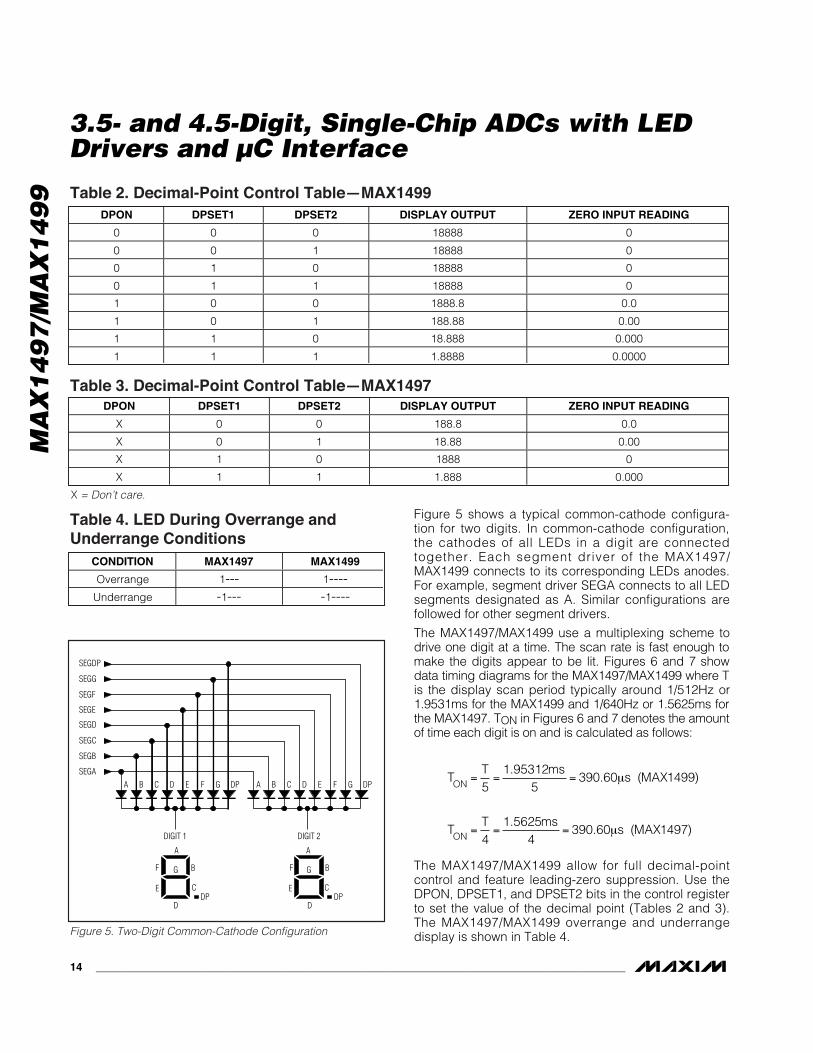
Figure 5 shows a typical common-cathode configura-tion for two digits. In common-cathode configuration,the cathodes of all LEDs in a digit are connectedtogether. Each segment driver of the MAX1497/MAX1499 connects to its corresponding LEDs anodes.For example, segment driver SEGA connects to all LEDsegments designated as A. Similar configurations arefollowed for other segment drivers.
The MAX1497/MAX1499 use a multiplexing scheme todrive one digit at a time. The scan rate is fast enough tomake the digits appear to be lit. Figures 6 and 7 showdata timing diagrams for the MAX1497/MAX1499 where Tis the display scan period typically around 1/512Hz or1.9531ms for the MAX1499 and 1/640Hz or 1.5625ms forthe MAX1497. TON in Figures 6 and 7 denotes the amountof time each digit is on and is calculated as follows:
The MAX1497/MAX1499 allow for full decimal-pointcontrol and feature leading-zero suppression. Use theDPON, DPSET1, and DPSET2 bits in the control registerto set the value of the decimal point (Tables 2 and 3).The MAX1497/MAX1499 overrange and underrangedisplay is shown in Table 4.
TT ms
s MAX
TT ms
s MAX
ON
ON
= = =
= = =
51 95312
5390 60 1499
41 5625
4390 60 1497
.. ( )
.. ( )
µ
µ
A
A
A
DIGIT 1 DIGIT 2
SEGDP
SEGG
SEGF
SEGE
SEGD
SEGC
SEGB
SEGA
D D
E E
G GF FB B
C CDP DP
B C D E F G DP A B C D E F G DP
Figure 5. Two-Digit Common-Cathode Configuration
Table 2. Decimal-Point Control Table—MAX1499DPON DPSET1 DPSET2 DISPLAY OUTPUT ZERO INPUT READING
0 0 0 18888 0
0 0 1 18888 0
0 1 0 18888 0
0 1 1 18888 0
1 0 0 1888.8 0.0
1 0 1 188.88 0.00
1 1 0 18.888 0.000
1 1 1 1.8888 0.0000
Table 3. Decimal-Point Control Table—MAX1497DPON DPSET1 DPSET2 DISPLAY OUTPUT ZERO INPUT READING
X 0 0 188.8 0.0
X 0 1 18.88 0.00
X 1 0 1888 0
X 1 1 1.888 0.000
X = Don’t care.
Table 4. LED During Overrange andUnderrange Conditions
CONDITION MAX1497 MAX1499
Overrange 1--- 1----Underrange -1--- -1----

MA
X1
49
7/M
AX
14
99
3.5- and 4.5-Digit, Single-Chip ADCs with LEDDrivers and µC Interface
______________________________________________________________________________________ 15
Leading-Zero SuppressionThe MAX1497/MAX1499 include a leading-zero sup-pression circuitry to turn off unnecessary zeros. Forexample, when DPSET1 and DPSET2 = [0,0], 0.0 is dis-played instead of 000.0. This feature saves a substan-tial amount of power from being wasted.
Interdigit BlankingThe MAX1497/MAX1499 also include an interdigitblanking circuitry. Without this feature, it is possible tosee a faint digit next to a digit that is completely on. Theinterdigit blanking circuitry prevents bleeding over intothe next digit for a short period of time. The typicalinterdigit blanking time is 4µs.
ReferenceThe MAX1497/MAX1499 reference sets the full-scalerange of the ADC transfer function. With a nominal2.048V reference, the ADC full-scale range is ±2V withthe RANGE bit equal to zero. With the RANGE bit set toone, the full-scale range is ±200mV. A decreased refer-ence voltage decreases full-scale range (see theTransfer Functions section).
The MAX1497/MAX1499 accept either an external ref-erence or an internal reference. The INTREF bit selectsthe reference mode (see the Control Register(Read/Write) section).
For internal reference operation, set the INTREF bit toone, connect REF- to GND, and bypass REF+ to GNDwith a 4.7µF capacitor. The internal reference providesa nominal 2.048V source between REF+ and GND. Theinternal reference temperature coefficient is typically40ppm/°C.
The default power-on state sets the MAX1497/MAX1499 to use the external reference with the INTREFbit cleared to zero. The external reference inputs, REF+and REF-, are fully differential. For a valid external refer-ence input, VREF+ must be greater than VREF-. BypassREF+ and REF- with a 0.1µF or greater capacitor toGND in external reference mode.
Figure 16 shows the MAX1497/MAX1499 operating withan external single-ended reference. In this mode, REF-is connected to GND and REF+ is driven with an exter-nal 2.048V reference. Bypass REF+ to GND with a0.47µF capacitor.
14 3 2 1 0 4 3 2 0 4
T
TON
DIGIT 4 (MSD)
DIGIT 3
DIGIT 2
DIGIT 1
DIGIT 0 (LSD)
DATAMSD LSD
Figure 6. LED Voltage Waveform—MAX1499
33 2 1 0 3 2 1 0 2 1
T
TON
DIGIT 3 (MSD)
DIGIT 2
DIGIT 1
DIGIT 0 (LSD)
DATAMSD LSD
Figure 7. LED Voltage Waveform—MAX1497

MA
X1
49
7/M
AX
14
99
3.5- and 4.5-Digit, Single-Chip ADCs with LEDDrivers and µC Interface
16 ______________________________________________________________________________________
Figure 15 shows the MAX1497/MAX1499 operating withan external differential reference. In this mode, REF- isconnected to the top of the strain gauge and REF+ isconnected to the midpoint of the resistor-divider of the supply.
Applications InformationSerial Interface
The SPI/QSPI/MICROWIRE serial interface consists of achip select (CS), a serial clock (SCLK), a data in (DIN),a data out (DOUT), and an asynchronous EOC output.EOC provides an asynchronous end-of-conversion sig-nal with a period of 200ms (fCLK = 4.9152MHz). TheMAX1497 updates the data register when EOC goeshigh. Data is valid in the ADC result registers whenEOC returns low. The serial interface provides accessto 12 on-chip registers, allowing control to all the powermodes and functional blocks. Table 5 lists the addressand read/write accessibility of all the registers.
A logic high on CS tri-states DOUT and causes theMAX1497/MAX1499 to ignore any signals on SCLK andDIN. To clock data in or out of the internal shift register,drive CS low. SCLK synchronizes the data transfer. Therising edge of SCLK clocks DIN into the shift register,and the falling edge of SCLK clocks DOUT out of theshift register. DIN and DOUT are transferred MSB first(data is left justified). Figures 8–12 show the detailedserial interface timing diagrams for the 8- and 16-bitread/write operations.
All communication with the MAX1497/MAX1499 beginswith a command byte on DIN, where the first logic oneon DIN is recognized as the START bit (MSB) for thecommand byte. The following seven clock cycles loadthe command into a shift register. These 7 bits specifywhich of the registers are accessed next, and whethera read or write operation takes place. Transitions on theserial clock after the command byte transfer, cause awrite or read from the device until the correct number of
CS
SCLK
DIN
DOUT
tCSH
tCL
tDS
tDH
tDV
tCH
tDO tTR
tCSHtCSS
Figure 8. Detailed Timing Diagram
SCLK
CS
DIN
DOUT
1 0 RS4 RS3 RS2 RS1 D7 D6 D5 D4 D3 D2 D1 D0D8D9RS0 x D15 D14 D13 D12 D11 D10
CONTROL BYTE DATA BYTE
Figure 9. Serial-Interface, 16-Bit, Write Timing Diagram

MA
X1
49
7/M
AX
14
99
3.5- and 4.5-Digit, Single-Chip ADCs with LEDDrivers and µC Interface
______________________________________________________________________________________ 17
SCLK
CS
DIN
DOUT
1 1 RS4 RS3 RS2 RS1 RS0 x
D7 D6 D5 D4 D3 D2 D1 D0
CONTROL BYTE DATA BYTE
Figure 12. Serial-Interface, 8-Bit, Read Timing Diagram
CS
SCLK
DIN
DOUT
1 0 RS4 RS3 RS2 RS1 D7 D6 D5 D4 D3 D2 D1 D0RS0 x
CONTROL BYTE DATA BYTE
Figure 10. Serial-Interface, 8-Bit, Write Timing Diagram
SCLK
CS
DIN
DOUT
1 1 RS4 RS3 RS2 RS1 RS0 x
D7 D6 D5 D4 D3 D2 D1 D0D8D9D15 D14 D13 D12 D11 D10
CONTROL BYTE DATA BYTE
Figure 11. Serial-Interface, 16-Bit, Read Timing Diagram

MA
X1
49
7/M
AX
14
99
3.5- and 4.5-Digit, Single-Chip ADCs with LEDDrivers and µC Interface
18 ______________________________________________________________________________________
bits have been transferred (8 or 16). Once this hasoccurred, the MAX1497/MAX1499 wait for the nextcommand byte. CS must not go high between datatransfers. If CS is toggled before the end of a write orread operation, the device mode may be unknown.Clock in 32 zeros to clear the device state and reset theinterface so it is ready to receive a new command byte.
On-Chip RegistersThe MAX1497/MAX1499 contain 12 on-chip registers.These registers configure the various functions of thedevice and allow independent reading of the ADCresults and writing to the LED display. Table 5 lists theaddress and size of each register.
The first of these registers is the status register. The 8-bit status register contains the status flags for the ADC.
The second register is the 16-bit control register. Thisregister sets the LED display controls, range modes,power-down modes, offset calibration, and the resetregister function (CLR). The third register is the 16-bitoverrange register, which sets the overrange limit of theanalog input. The fourth register is the 16-bit under-range register, which sets the underrange limit of theanalog input. Registers 5 through 7 contain the displaydata for the individual segments of the LED. The eighthregister contains the custom offset value. The ninth reg-ister contains the 16 MSBs of the ADC conversionresult. The 10th register contains the LED data. The11th register contains the peak analog input value. Thelast register contains the lower four LSBs of the 20-bitADC conversion result.
REGISTERN0.
ADDRESSRS [4:0]
NAME WIDTH ACCESS
1 00000 Status register 8 Read only
2 00001 Control register 16 R/W
3 00010 Overrange register 16 R/W
4 00011 Underrange register 16 R/W
5 00100 LED segment-display register 1 16 R/W
6 00101 LED segment-display register 2 16 R/W
7 00110 LED segment-display register 3 8 R/W
8 00111 ADC custom offset register 16 R/W
9 01000 ADC result register 1 (16 MSBs) 16 Read only
10 01001 LED data register 16 R/W
11 01010 Peak register 16 Read only
12 10100 ADC result register 2 (4 LSBs) 8 Read only
— All other addresses Reserved — —
Table 5. Register Address Table
6kΩ
6kΩ
DOUTDOUT
GNDGND
DVDD
CLOAD50pF
CLOAD50pF
A) VOH TO HIGH-Z B) VOL TO HIGH-Z
Figure 13. Load Circuits for Disable Time
6kΩ
6kΩ
DOUTDOUT
GNDGND
DVDD
CLOAD50pF
CLOAD50pF
B) HIGH-Z TO VOH AND VOL TO VOH B) HIGH-Z TO VOL AND VOH TO VOL
Figure 14. Load Circuits for Enable Time

MA
X1
49
7/M
AX
14
99
3.5- and 4.5-Digit, Single-Chip ADCs with LEDDrivers and µC Interface
______________________________________________________________________________________ 19
Default values: 00h
This register contains the status of the conversionresults.
SIGN: Latched negative-polarity indicator. Latcheshigh when the result is negative. Clears by reading thestatus register, unless the condition remains true.
OVER: Overrange bit. Latches high if an overrangecondition occurs (the ADC result is larger than thevalue in the overrange register). Clears by reading thestatus register, unless the condition remains true.
UNDER: Underrange bit. Latches high if an under-range condition occurs (the ADC result is less than the
value in the underrange register). Clears by reading thestatus register, unless the condition remains true.
LOW_BATT: Low-battery bit. Latches high if the volt-age at the LOWBATT is lower than 2.048V (typ). Clearsby reading the status register, unless the conditionremains true. For the MAX1497, LOWBATT is not usedand the LOWBATT bit always returns to zero.
DRDY: Data ready bit. Latches high to indicate a com-pleted conversion result with valid data. Read the ADCresult register to clear this bit.
Control and Status RegistersCommand Byte (Write Only)
Status Register (Read Only)
MSB LSB
Bit 7 Bit 6 Bit 5 Bit 4 Bit 3 Bit 2 Bit 1 Bit 0
START(1) R/W RS4 RS3 RS2 RS1 RS0 X
MSB LSB
SIGN OVER UNDER LOW_BATT DRDY 0 0 0
Control Register (Read/Write)
MSB
Bit 15 Bit 14 Bit 13 Bit 12 Bit 11 Bit 10 Bit 9 Bit 8
SPI/ADC EXTCLK INTREF DPON DPSET2 DPSET1 PD_DIG PD_ANA
LSB
Bit 7 Bit 6 Bit 5 Bit 4 Bit 3 Bit 2 Bit 1 Bit 0
HOLD PEAK RANGE CLR SEG_SEL OFFSET_CAL1OFFSET_
CAL2ENABLE
START: Start bit. The first 1 clocked into the MAX1497/MAX1499 is the first bit of the command byte.
(R/W): Read/Write. Set this bit to 1 to read from thespecified register. Set this bit to zero to write to theselected register. Note that certain registers are read
only. Write commands to a read-only register areignored.
(RS4–RS0): Register address bits. RS4 to RS0 specifywhich register is accessed.
X: Don’t care.
Default values: 0001h
This register is the primary control register for theMAX1497/MAX1499. It is a 16-bit read/write register. Itis used to indicate the desired clock and referencesource. It sets the LED display controls, range modes,power-down modes, offset calibration, and the resetregister function (CLR).
ENABLE: (default = 1) LED driver enable bit. When set to1, the MAX1497/MAX1499 enables the LED display dri-vers. A 0 in this location disables the LED display drivers.
OFFSET_CAL2: (default = 0) Enhanced offset-calibra-tion start bit (MAX1499, RANGE = 1). To achieve thelowest possible offset in the ±200mV input range, per-form an enhanced offset calibration by setting this bit to

MA
X1
49
7/M
AX
14
99
3.5- and 4.5-Digit, Single-Chip ADCs with LEDDrivers and µC Interface
20 ______________________________________________________________________________________
1. The calibration takes about nine cycles (1800ms).After the calibration completes, set this bit to zero toresume ADC conversions.
OFFSET_CAL1: (default = 0) Automatic offset calibra-tion enable bit. When set to 1, the MAX1497/MAX1499 disable automatic offset calibration. When thisbit is set to zero, automatic offset calibration is enabled.
SEG_SEL: (default = 0) SEG_SEL segment selectionbit. When set to 1, the LED segment drivers use theLED segment registers to display individual segmentsthat can form letters or numbers or other information onthe display. The LED data register is not displayed.Send the data first to the LED segment-display regis-ters and then set this bit high.
CLR: (default = 0) Clear all registers bit. When set to 1,all registers reset to their power-on reset states after CSmakes a low-to-high transition.
RANGE: (default = 0) Input range select bit. When setto zero, the input voltage range is ±2V. When set to 1,the input voltage range is ±200mV.
PEAK: (default = 0) Peak bit. When set to 1 (and theHOLD bit is set to zero), the LED shows the resultstored in the peak register (see Table 6).
HOLD: (default = 0) Hold bit. When set to 1, the LEDregister does not update from the ADC conversionresults and holds the last result on the LED. TheMAX1497/MAX1499 continue to perform conversionsduring HOLD (Table 1).
PD_ANA: (default = 0) Power-down analog select bit.When set to 1, the analog circuits (analog modulatorand ADC input buffers) go into the power-down mode.When set to zero, the device is in full power-up mode.
PD_DIG: (default = 0) Power-down digital select bit.When set to 1, the digital circuits (digital filter and LEDdrivers) go into power-down mode. This also resets thevalues of the internal SRAM in the digital filter to zeros.When set to zero, the device returns to full power-upmode. When powering down PD_DIG, power down theLED segment drivers by clearing the ENABLE bit to zero.
DPSET[2:1]: (default = 00) Decimal-point selection bits(Table 2 and 3).
DPON: (default = 0) Decimal-point enable bit (Tables 2and 3).
INTREF: (default = 0) Reference select bit. For internalreference operation, set INTREF to 1. For external refer-ence operation, set INTREF to zero.
EXTCLK: (default = 0) External clock select bit. TheEXTCLK bit controls selection of the internal clock or anexternal clock source. A 1 in this location selects thesignal at the CLK input as the clock source. A zero inthis location selects and powers up the internal clockoscillator.
SPI/ADC: (default = 0) Display select bit. The SPI/ADC bitcontrols selection of the data fed into LED data register. A1 in this location selects SPI/QSPI/ MICROWIRE data(user writes this data to the LED data register). A zero inthis location selects the ADC result register data, unlesshold or peak functions are active (Table 1).
Note: When changing any one of the following controlbits: OFFSET_CAL1, RANGE, PD_ANA, PD_DIG,INTREF, and EXTCLK, wait 800ms before reading theADC results.
Overrange Register (Read/Write)
MSB LSB
D15 D14 D13 D12 D11 D10 D9 D8 D7 D6 D5 D4 D3 D2 D1 D0
Default values: 7CF0h (for 3.5-digit, +1999)
4E1Fh (for 4.5-digit, +19,999)
The overrange register is a 16-bit read/write register(D15 is the MSB). When the conversion result exceedsthe value in the overrange register, the OVER bit in thestatus register latches to 1. The LED shows a 1 followed
by four dashes for the MAX1499 or a 1 followed bythree dashes for the MAX1497 (Table 4).
The data is represented in two’s complement format.

MA
X1
49
7/M
AX
14
99
3.5- and 4.5-Digit, Single-Chip ADCs with LEDDrivers and µC Interface
______________________________________________________________________________________ 21
Default values: 8300h (for 3.5-digit, -2000)
B1E0h (for 4.5-digit, -20,000)
The underrange data register is 16-bit read/write regis-ter (D15 is the MSB). When the conversion result fallsbelow the value in the underrange register, the UNDRbit in the status register sets to 1. The LED shows a -1
followed by four dashes for the MAX1499 or a -1 fol-lowed by three dashes for the MAX1497 (Table 4).
The data is represented in two’s complement format.
Default values: 0000h
Underrange Register (Read/Write)
MSB LSB
D15 D14 D13 D12 D11 D10 D9 D8 D7 D6 D5 D4 D3 D2 D1 D0
LED Segment-Display Register 1 (Read/Write)
MSB
Bit 15 Bit 14 Bit 13 Bit 1 Bit 11 Bit 10 Bit 9 Bit 8
A1 G1 D1 F1 E1 DP2 X B0
LSB
Bit 7 Bit 6 Bit 5 Bit 4 Bit 3 Bit 2 Bit 1 Bit 0
C0 A0 G0 D0 F0 E0 DP1 0
LED segment-display register 1 is a 16-bit read/writeregister. When the LED bit (in the control register) is setto 1, the MAX1497/MAX1499 provide direct access toindividual LED segments. The bits in the LED segment-display register determine if a segment is on or off.Write a zero to turn on a segment and a 1 to turn off asegment.
DP1: Segment DP driver bit of digit 1. The default valueturns on the LED segment.
E0: Segment E driver bit of digit 0. The default valueturns on the LED segment.
F0: Segment F driver bit of digit 0. The default valueturns on the LED segment.
D0: Segment D driver bit of digit 0. The default valueturns on the LED segment.
G0: Segment G driver bit of digit 0. The default valueturns on the LED segment.
A0: Segment A driver bit of digit 0. The default valueturns on the LED segment.
C0: Segment C driver bit of digit 0. The default valueturns on the LED segment.
B0: Segment B driver bit of digit 0. The default valueturns on the LED segment.
X: Don’t care.
DP2: Segment DP driver bit of digit 2. The default valueturns on the LED segment.
E1: Segment E driver bit of digit 1. The default valueturns on the LED segment.
F1: Segment F driver bit of digit 1. The default valueturns on the LED segment.
D1: Segment D driver bit of digit 1. The default valueturns on the LED segment.
G1: Segment G driver bit of digit 1. The default valueturns on the LED segment.
A1: Segment A driver bit of digit 1. The default valueturns on the LED segment.

MA
X1
49
7/M
AX
14
99
3.5- and 4.5-Digit, Single-Chip ADCs with LEDDrivers and µC Interface
22 ______________________________________________________________________________________
Default values: 0000h
LED segment-display register 2 is a 16-bit read/writeregister. When the SEG_SEL bit (in the control register)is set to 1, the MAX1497/MAX1499 provide directaccess to individual LED segments. The bits in the LEDsegment-display register determine if a segment is onor off. Write a zero to turn on a segment and a 1 to turnoff a segment.
C1: Segment C driver bit of digit 1. The default valueturns on the LED segment.
B1: Segment B driver bit of digit 1. The default valueturns on the LED segment.
MINUS: Segment minus driver bit. The default valueturns on the LED minus segment. Setting this bit to 1enables the plus sign on the LED display.
DP3: Segment DP driver bit of digit 3. The default valueturns on the LED segment.
E2: Segment E driver bit of digit 2. The default valueturns on the LED segment.
F2: Segment F driver bit of digit 2. The default valueturns on the LED segment.
D2: Segment D driver bit of digit 2. The default valueturns on the LED segment.
G2: Segment G driver bit of digit 2. The default valueturns on the LED segment.
A2: Segment A driver bit of digit 2. The default valueturns on the LED segment.
C2: Segment C driver bit of digit 2. The default valueturns on the LED segment.
B2: Segment B driver bit of digit 2. The default valueturns on the LED segment.
DP4: Segment DP driver bit of digit 4. The default valueturns on the LED segment (MAX1499 only).
E3: Segment E driver bit of digit 3. The default valueturns on the LED segment (MAX1499 only).
F3: Segment F driver bit of digit 3. The default valueturns on the LED segment (MAX1499 only).
LED Segment-Display Register 2 (Read/Write)
MSB
Bit 15 Bit 14 Bit 13 Bit 1 Bit 11 Bit 10 Bit 9 Bit 8
F3 E3 DP4 MINUS B2 C2 A2 G2
LSB
Bit 7 Bit 6 Bit 5 Bit 4 Bit 3 Bit 2 Bit 1 Bit 0
D2 F2 E2 DP3 X B1 C1 0
LED Segment-Display Register 3 (Read/Write)
MSB LSB
X X BC_ B3 C3 A3 G3 D3
Default values: 00h
LED segment-display register 3 is an 8-bit read/writeregister. When the SEG_SEL bit (in the control register)is set to 1, the MAX1497/MAX1499 provide directaccess to individual LED segments. The bits in the LEDsegment-display register determine if a segment is onor off. Write a zero to turn on a segment and a 1 to turnoff a segment.
D3: Segment D driver bit of digit 3. The default valueturns on the LED segment (MAX1499 only).
G3: Segment G driver bit of digit 3. The default valueturns on the LED segment (MAX1499 only).
A3: Segment A driver bit of digit 3. The default valueturns on the LED segment (MAX1499 only).
C3: Segment C driver bit of digit 3. The default valueturns on the LED segment (MAX1499 only).
B3: Segment B driver bit of digit 3. The default valueturns on the LED segment (MAX1499 only).
BC_: Segment B and C driver bit of digit 3 (3.5 digits)or Digit 4 (4.5 digits). The default value turns on theLED segment.
X: Don’t care.

MA
X1
49
7/M
AX
14
99
3.5- and 4.5-Digit, Single-Chip ADCs with LEDDrivers and µC Interface
______________________________________________________________________________________ 23
Default values: 0000h
In addition to automatic offset calibration, theMAX1497/MAX1499 offer a user-defined custom offset16-bit read/write register. The final result of the ADCconversion is the input after autocalibration minus
the value in the custom offset. The custom offset valueis stored in this register. D15 is the MSB. The data isrepresented in two’s complement format.
ADC Custom Offset-Calibration Register (Read/Write)
MSB LSB
D15 D14 D13 D12 D11 D10 D9 D8 D7 D6 D5 D4 D3 D2 D1 D0
ADC Result Register 1 (Read Only)
MSBLSB
(MAX1497)LSB
(MAX1499)
D15 D14 D13 D12 D11 D10 D9 D8 D7 D6 D5 D4 D3 D2 D1 D0
Default values: 0000h
ADC result register 1 is a 16-bit read-only register. Thisregister stores the 16 MSBs of the ADC result. The datais represented in two’s complement format.
For the MAX1499, the data is 16-bit and D15 is theMSB. For the MAX1497, the data is 12-bit, D15 is theMSB, and D4 is the LSB.
Default values: 0000h
The LED data register is a 16-bit read/write register.This register updates from ADC result register 1 or fromthe serial interface by selecting the SPI/ADC bit in thecontrol register. The data is represented in two’s com-plement format.
For the MAX1499, the data is 16-bit and D15 is theMSB. For the MAX1497, the data is 12-bit, D15 is theMSB, and D4 is the LSB, followed by 4 trailing sub-bits.
LED Data Register (Read/Write)
MSBLSB
(MAX1497)LSB
(MAX1499)
D15 D14 D13 D12 D11 D10 D9 D8 D7 D6 D5 D4 D3 D2 D1 D0
ADC Result Register 2 (Read Only)
MSB LSB
D3 D2 D1 D0 0 0 0 0
Default values: 00h
ADC result register 2 is an 8-bit read-only register. Thisregister stores the 4 LSBs of the ADC result.
Use this result with the result in ADC result-register 1 toform a 20-bit two’s complement conversion result.

MA
X1
49
7/M
AX
14
99
3.5- and 4.5-Digit, Single-Chip ADCs with LEDDrivers and µC Interface
24 ______________________________________________________________________________________
PEAK Register (Read Only)
MSBLSB
(MAX1497)LSB
(MAX1499)
D15 D14 D13 D12 D11 D10 D9 D8 D7 D6 D5 D4 D3 D2 D1 D0
Default values: B1E0h
The peak data register is a 16-bit read only register. Setthe PEAK bit to 1 to enable the PEAK function. This reg-ister stores the peak value of the ADC conversionresult. First, the current ADC result is saved to thePEAK register, then the new ADC conversion result iscompared to this value. If the new value is larger thanthe value in the peak register, the MAX1497/MAX1499save the new value to the peak register. If the new
value is less than the value in the peak register, thevalue in the peak register remains unchanged. Set thePEAK bit to zero to clear the value in the PEAK register.
The data is represented in two’s complement format.
For the MAX1499, the data is 16-bit and D15 is the MSB.For the MAX1497, the data is 12-bit, D15 is the MSB,and D4 is the LSB followed by 4 trailing sub-bits.

MA
X1
49
7/M
AX
14
99
3.5- and 4.5-Digit, Single-Chip ADCs with LEDDrivers and µC Interface
______________________________________________________________________________________ 25
Figure 16. Thermocouple Application with the MAX1497/MAX1499Figure 15. Strain-Gauge Application with the MAX1497/MAX1499
MAX1497MAX1499
AVDD DVDD
DOUTDINSCLK
4.7µF
0.1µF
0.1µF
0.1µF
0.1µF
0.1µF
ANALOG SUPPLY
FERRITEBEAD
RREF
R
R
ACTIVEGAUGE
DUMMYGAUGE
REF+
REF-
AIN+
AIN-
GNDEOCCS
4.7µF
0.1µF
MAX1497MAX1499
MAX6062
+5V
+2.048V
TEMPSENSOR
THERMOCOUPLEJUNCTION
0.1µF
0.47µF
SPIµC
AIN+
AIN-
REF+
REF-
GND
Power-On ResetAt power-on, the serial interface, logic LED drivers, dig-ital filter, and modulator circuits reset. The registersreturn to their default values. Allow time for the refer-ence to settle before starting calibration.
Offset CalibrationThe MAX1497/MAX1499 offer on-chip offset calibration.The device offset calibrates during every conversionwhen the OFFSET_CAL1 bit is zero in the control regis-ter. Enhanced offset calibration is only needed in theMAX1499 when the RANGE bit = 1. It is performed ondemand by setting the OFFSET_CAL2 bit to 1.
Enhanced Offset CalibrationEnhanced offset calibration is a more accurate calibra-tion method that is needed in the case of the ±200mVrange and 4.5-digit resolution. The MAX1499 performsthe enhanced calibration on demand by setting theOFFSET_CAL2 bit to 1.
Power-Down ModesThe MAX1497/MAX1499 feature independent power-down control of the analog and digital LED drivers cir-cuitry. Writing a 1 to the PD_DIG and PD_ANA bits inthe control word, powers down the analog and digitalcircuitry, reducing the supply current to 268µA (typ).PD_DIG powers down the digital filter, while PD_ANA
powers down the analog modulator and ADC inputbuffers. Writing a zero to the ENABLE bit in the controlword, powers down the LED drivers.
PeakThe MAX1497/MAX1499 feature peak detection circuit-ry. When activated (PEAK bit = 1), the devices displayonly the highest voltage measured to the LED.
HoldThe MAX1497/MAX1499 feature data-hold circuitry.When activated (HOLD bit = 1), the device displays thecurrent reading on the LED.
Low BatteryThe MAX1499 features a low-battery detection input.When the voltage at LOWBATT drops below 2.048V(typ), the LOWBATT bit of the status register goes high.
Strain-Gauge MeasurementConnect the differential inputs of the MAX1497/MAX1499to the bridge network of the strain gauge. In Figure 15,the analog supply voltage powers the bridge networkand the MAX1497/MAX1499 along with the referencevoltage. The MAX1497/MAX1499 handle an analog inputvoltage range of ±200mV and ±2V full scale. The ana-log/reference inputs of the parts allow the analog inputrange to have an absolute value of anywhere between -2.2V and +2.2V.

MA
X1
49
7/M
AX
14
99
3.5- and 4.5-Digit, Single-Chip ADCs with LEDDrivers and µC Interface
26 ______________________________________________________________________________________
Thermocouple MeasurementFigure 16 shows a connection from a thermocouple tothe MAX1497/MAX1499. In this application, theMAX1497/MAX1499 take advantage of the on-chipinput buffers that allow large source impedances on thefront end. The decoupling capacitors reduce noisepickup from the thermocouple leads. To place the dif-ferential voltage from the thermocouple at a suitablecommon-mode voltage, the AIN- input of the MAX1497/MAX1499 is biased to GND. Use an external tempera-ture sensor, such as the DS75, and a µC to performcold-junction temperature compensation.
Transfer FunctionsFigures 17–20 show the transfer functions of theMAX1497/MAX1499. The output data is stored in theADC data register in two’s complement.
The transfer function for the MAX1499 with AIN+ - AIN-≥ 0, RANGE = 0 is:
COUNTSV VV V
AIN AIN
REF REF . ,=
×+
+
− −
− −1 024 20 000
7CFh7CFh
002h001h
000h
FFFh
FFEhFFDh
830h<830h
-200mV 0
ANALOG INPUT VOLTAGE
+200mV
ADC RESULTLED
1 - - -
1999
21
0
- 0- 1- 2
-1999- 1 - - -
-100µV 100µV
Figure 19. MAX1497 Transfer Function, ±200mV Range
>7CFh7CFh
002h001h
000h
FFFh
FFEhFFDh
830h<830h
-2V 0
ANALOG INPUT VOLTAGE
+2V
ADC RESULTLED
1 - - -
1999
21
0
- 0- 1- 2
-1999- 1 - - -
-1mV 1mV
Figure 20. MAX1497 Transfer Function, ±2V Range
>4E1Fh4E1Fh
0002h0001h
0000h
FFFFh
FFFEhFFFDh
B1E0h<B1E0h
-2V 0
ANALOG INPUT VOLTAGE
+2V
ADC RESULTLED
1 - - - -
19,999
21
0
- 0- 1- 2
-19,999- 1 - - - -
-100µV 100µV
Figure 17. MAX1499 Transfer Function, ±2V Range
4E1Fh4E1Fh
0002h00001h
0000h
FFFFh
FFFEhFFFDh
B1E0h<B1E0h
-200mV 0
ANALOG INPUT VOLTAGE
+200mV
ADC RESULTLED
1 - - - -
19,999
21
0
- 0- 1- 2
-19,999- 1 - - - -
-10µV 10µV
Figure 18. MAX1499 Transfer Function, ±200mV Range

The transfer function for the MAX1499 with AIN+ - AIN-< 0, RANGE = 0 is:
The transfer function for the MAX1497 with AIN+ - AIN-≥ 0, RANGE = 0 is:
The transfer function for the MAX1497 with AIN+ - AIN-< 0, RANGE = 0 is:
The transfer function for the MAX1499 with AIN+ - AIN-≥ 0, RANGE = 1 is:
The transfer function for the MAX1499 with AIN+ - AIN-< 0, RANGE = 1 is:
The transfer function for the MAX1497 with AIN+ - AIN-≥ 0, RANGE = 1 is:
The transfer function for the MAX1497 with AIN+ - AIN-< 0, RANGE = 1 is:
Supplies, Layout, and BypassingPower up AVDD and DVDD (MAX1499) and VDD(MAX1497) before applying an analog input and exter-nal reference voltage to the device. If this is not possi-ble, limit the current into these inputs to 50mA. Whenthe analog and digital supplies come from the samesource, isolate the digital supply from the analog sup-ply with a low-value resistor (10Ω) or ferrite bead. Forbest performance, ground the MAX1497/MAX1499 tothe analog ground plane of the circuit board.
Avoid running digital lines under the device, becausethey may couple noise onto the die. Run the analogground plane under the MAX1497/MAX1499 to mini-mize coupling of digital noise. Make the power-supplylines to the MAX1497/MAX1499 as wide as possible toprovide low-impedance paths and reduce the effects ofglitches on the power-supply line.
Shield fast-switching signals, such as clocks, with digitalground to avoid radiating noise to other sections of theboard. Avoid running clock signals near the analoginputs. Avoid crossover of digital and analog signals.Running traces that are on opposite sides of the board atright angles to each other reduces feedthrough effects.A microstrip technique is best, but is not always possiblewith double-sided boards. With this technique, the com-ponent side of the board is dedicated to ground planeswhile signals are placed on the solder side.
Good decoupling is important when using high-resolutionADCs. Decouple the supplies with 0.1µF ceramic capaci-tors to GND. Place these components as close to thedevice as possible to achieve the best decoupling.
Segment-Current SelectionA resistor from ISET to ground sets the current for eachLED segment. See Table 6 for more detail. Use the fol-lowing formula to set the segment current:
RISET values below 25kΩ increase the ISEG. However,the internal current-limit circuit limits the ISEG to less than30mA. At higher ISEG values, the proper operation of thedevice is not guaranteed. In addition, the power dissipat-ed may exceed the package power dissipation limit.
IV
RSEGISET
=
×
1 25400
.COUNTS
V VV V
AIN AIN
REF REF . = ×
× ++
+
− −
− −1 024 2000 10 1
COUNTSV V
V VAIN AIN
REF REF
. = ×
×+
−
+−
−
−
1 024 2000 10
COUNTSV VV V
AIN AIN
REF REF . , = ×
× ++
+
− −
− −1 024 20 000 10 1
COUNTSV VV V
AIN AIN
REF REF . , =
× ×+
+
− −
− −1 024 20 000 10
COUNTSV VV V
AIN AIN
REF REF . = ×
++
+
− −
− −1 024 2000 1
COUNTSV V
V VAIN AIN
REF REF
. = ×
+−
+−
−
−
1 024 2000
COUNTSV VV V
AIN AIN
REF REF . , = ×
++
+
− −
− −1 024 20 000 1
MA
X1
49
7/M
AX
14
99
3.5- and 4.5-Digit, Single-Chip ADCs with LEDDrivers and µC Interface
______________________________________________________________________________________ 27
RISET (kΩ) ISEG (mA)
25 20
50 10
100 5
500 1
>2500 LED driver disabled
Table 6. Segment Current Selection

MA
X1
49
7/M
AX
14
99
3.5- and 4.5-Digit, Single-Chip ADCs with LEDDrivers and µC Interface
28 ______________________________________________________________________________________
Choosing Supply Voltage to MinimizePower Dissipation
The MAX1497/MAX1499 drive a peak current of25.5mA into LEDs with a 2.2V forward-voltage dropwhen operated from a supply voltage of at least 3.0V.Therefore, the minimum voltage drop across the inter-nal LED drivers is (3.0V - 2.2V) = 0.8V. The MAX1497/MAX1499 sink (8 x 25.5mA = 204mA) when the outputsare operating and LED segment drivers are at full cur-rent. For a 3.3V supply, the MAX1497/MAX1499 dissi-pate (3.3V - 2.2V) x 204 = 224.4mW. If a higher supplyvoltage is used, the driver absorbs a higher voltage,and the driver’s power dissipation increases according-ly. However, if the LEDs used have a higher forwardvoltage drop than 2.2V, the supply voltage must beraised accordingly to ensure that the driver always hasat least 0.8V headroom.
For a VLED supply voltage of 2.7V, the maximum LEDforward voltage is 1.9V to ensure 0.8V driver headroom.The voltage drop across the drivers with a nominal +5Vsupply (5.0V - 2.2V = 2.8V) is almost three times thedrop across the drivers with a nominal 3.3V supply(3.3V - 2.2V = 1.1V). Therefore, the driver’s power dissi-pation increases three times. The power dissipation inthe part causes the junction temperature to rise accord-ingly. In the high ambient temperature case, the totaljunction temperature may be very high (>+125°C). Athigher junction temperatures, the ADC performancedegrades. To ensure the dissipation limit for theMAX1497/MAX1499 is not exceeded and the ADC per-formance is not degraded, a diode can be insertedbetween the power supply and VLED.
Computing Power DissipationThe following can be used to compute power dissipa-tion:
PD = (VLED x IVLED ) + (VLED - VDIODE) (DUTY x ISEG x N) + VSUPPLY x ISUPPLY
VLED = LED driver supply voltage
IVLED = VLED bias current
VDIODE = LED forward voltage
DUTY = segment ON time during each digit ON time
ISEG = segment current set by RISET
N = number of segments driven (worst case is eight)
VSUPPLY = supply voltage of the part
ISUPPLY = supply current from VDD for the MAX1497 orAVDD + DVDD for the MAX1499
Dissipation ExampleFor ISEG = 25.5mA, N = 8, DUTY = 127 / 128, VDIODE =1.5V at 25.5mA, VLED = VSUPPLY = 5.25V:
PD = (5.25 x 2mA) + (5.25V - 1.5) [(127 / 128) x 25.5mA x 8)] + 5.25 x 1.080mA
PD = 0.7751W
28-Pin SSOP Package ExampleFor the 28-pin SSOP package (TJA = 1 / 0.009496 =+105.3°C/W), the maximum allowed ambient tempera-ture TA is given by:
TJ (max) = TA + (PD x TJA) = +125°C = TA + (0.7751W x +105.3°C/W)
TA = +43°C
Thus, the device cannot operate safely at a maximumpackage temperature of +85°C. The power dissipatesin the part need to be lowered.
(PD x TJA) max = (+125°C) - (+85°C) = +40°C
PD (max) = +40°C /+105.3°C/W = 380mW
(VLED - VDIODE) = [380mW - (5.25V x 2mA) - 5.25V x1.080mA] / [(127 / 128) x 25.5mA x 8]
VLED - VDIODE = 1.854V
VLED - VDIODE should have the following condition toensure it operates safely:
0.8V < VLED - VDIODE < 2.08V
28-Pin PDIP Package ExamplePD x TJA (max) = (+125°C) - (+85°C) = +40°C
PD (max) = +40°C /+70°C/W = 571mW
VLED - VDIODE = [571mW - (5.25V x 2mA) - 5.25V x1.080mA] / [(127 / 128) x 25.5mA x 8]
VLED - VDIODE = 2.80V
For a 28-pin PDIP package, VLED - VDIODE shouldhave the following condition to ensure it operates safe-ly:
0.8V < VLED - VDIODE < 3.18V
32-Pin TQFP PackageThe MAX1499 TQFP package can operate safely for allsupply voltages provided VDIODE > 1.5V.

DefinitionsINL
Integral nonlinearity (INL) is the deviation of the values onan actual transfer function from a straight line. This straightline is either a best-straight-line fit or a line drawn betweenthe end points of the transfer function, once offset andgain errors have been nullified. INL for the MAX1497/MAX1499 is measured using the endpoint method.
DNLDifferential nonlinearity (DNL) is the difference betweenan actual step width and the ideal value of ±1 LSB. ADNL error specification of less than ±1 LSB guaranteesno missing codes and a monotonic transfer function.
Rollover ErrorRollover error is defined as the absolute-value differ-ence between a near positive full-scale reading andnear negative full-scale reading. Rollover error is testedby applying a full-scale positive voltage, swappingAIN+ and AIN-, and adding the results.
Zero Input ReadingIdeally, with AIN+ connected to AIN-, the MAX1497/MAX1499 digital ADC result is 0000h. Zero input read-ing is the measured deviation from the ideal 0x0000and the actual measured point.
Gain ErrorGain error is the amount of deviation between the mea-sured full-scale transition point and the ideal full-scaletransition point.
Common-Mode RejectionCommon-mode rejection (CMR) is the ability of adevice to reject a signal that is common to both inputterminals. The common-mode signal can be either anAC or a DC signal or a combination of the two. CMR isoften expressed in decibels.
Normal-Mode 50Hz and 60Hz Rejection(Simultaneously)
Normal-mode rejection is a measure of how much outputchanges when a 50Hz and a 60Hz signal is injected intoonly one of the differential inputs. The MAX1497/MAX1499 sigma-delta converter uses its internal digitalfilter to provide normal-mode rejection to both 50Hz and60Hz power-line frequencies simultaneously.
Power-Supply Rejection RatioPower-supply rejection ratio (PSRR) is the ratio of the inputsupply change (in volts) to the change in the converteroutput (in volts). It is typically measured in decibels.
MA
X1
49
7/M
AX
14
99
3.5- and 4.5-Digit, Single-Chip ADCs with LEDDrivers and µC Interface
______________________________________________________________________________________ 29
28
27
26
25
24
23
22
21
20
19
18
17
16
15
1
2
3
4
5
6
7
8
9
10
11
12
13
14
SEGDP
SEGG
SEGF
VLED
SEGE
SEGD
DIG0
SEGC
SEGB
SEGA
DIG3
DIG2
GLED
DIG1
DOUT
SCLK
DIN
CS
EOC
CLK
VDD
GND
AIN-
AIN+
ISET
REF+
REF-
VNEG
SSOP/PDIP
TOP VIEW
MAX1497
TOP VIEW
MAX1499
TQFP
32 28293031 252627
V NEG
LOW
BATT
LED_
EN
SEGD
P
REF-
SEGG
SEGF
VLED
10 13 1514 1611 129
DIN
DOUT
SCLK
DIG1
DIG0
GLED
17
18
19
20
21
22
23 SEGD
24 SEGE
SEGC
SEGB
SEGA
DIG4
DIG3
DIG2
2
3
4
5
6
7
8CLK
DVDD
AVDD
GND
ISET
AIN-
AIN+
1REF+
CSEOC
Pin Configurations
Chip InformationTRANSISTOR COUNT: 80,000
PROCESS: BiCMOS

MA
X1
49
7/M
AX
14
99
3.5- and 4.5-Digit, Single-Chip ADCs with LEDDrivers and µC Interface
30 ______________________________________________________________________________________
MAX1497
0.1µF 4.7µF
µC
0.1µF10µF
2.7V TO5.25V
AIN+
AIN-
VLED
VDD
ISET VNEG GND REF- REF+ GLED
CLK
SCLK
DIN
DOUT
CS
EOC
DIG0–DIG3DIGIT
CONNECTIONS
SEGA–SEGDPSEGMENT
CONNECTIONSVIN
25kΩ
Typical Operating Circuits
MAX1499
0.1µF 4.7µF
µC
0.1µF
0.1µF
10µF
10µF
LISO
2.7V TO5.25V
AIN+
AIN-
VLED
DVDD
AVDD
ISET VNEG GND REF- REF+ GLED
CLK
SCLK
DIN
DOUT
CS
EOC
DIG0–DIG4DIGIT
CONNECTIONS
SEGA–SEGDPSEGMENT
CONNECTIONSVIN
LOWBATT
25kΩ

MA
X1
49
7/M
AX
14
99
3.5- and 4.5-Digit, Single-Chip ADCs with LEDDrivers and µC Interface
______________________________________________________________________________________ 31
32L/
48L,
TQFP
.EP
S
Package Information(The package drawing(s) in this data sheet may not reflect the most current specifications. For the latest package outline information,go to www.maxim-ic.com/packages.)

MA
X1
49
7/M
AX
14
99
3.5- and 4.5-Digit, Single-Chip ADCs with LEDDrivers and µC Interface
32 ______________________________________________________________________________________
SS
OP
.EP
S
PACKAGE OUTLINE, SSOP, 5.3 MM
11
21-0056 CREV.DOCUMENT CONTROL NO.APPROVAL
PROPRIETARY INFORMATION
TITLE:
NOTES:1. D&E DO NOT INCLUDE MOLD FLASH.2. MOLD FLASH OR PROTRUSIONS NOT TO EXCEED .15 MM (.006").3. CONTROLLING DIMENSION: MILLIMETERS.4. MEETS JEDEC MO150.5. LEADS TO BE COPLANAR WITHIN 0.10 MM.
7.90H
L
0∞
0.301
0.025
8∞
0.311
0.037
0∞
7.65
0.63
8∞
0.95
MAX
5.38
MILLIMETERS
B
C
D
E
e
A1
DIM
A
SEE VARIATIONS
0.0256 BSC
0.010
0.004
0.205
0.002
0.015
0.008
0.212
0.008
INCHES
MIN MAX
0.078
0.65 BSC
0.25
0.09
5.20
0.05
0.38
0.20
0.21
MIN
1.73 1.99
MILLIMETERS
6.07
6.07
10.07
8.07
7.07
INCHES
D
D
D
D
D
0.239
0.239
0.397
0.317
0.278
MIN
0.249
0.249
0.407
0.328
0.289
MAX MIN
6.33
6.33
10.33
8.33
7.33
14L
16L
28L
24L
20L
MAX N
A
D
e A1 L
C
HE
N
12
B
0.068
Package Information (continued)(The package drawing(s) in this data sheet may not reflect the most current specifications. For the latest package outline information,go to www.maxim-ic.com/packages.)

MA
X1
49
7/M
AX
14
99
3.5- and 4.5-Digit, Single-Chip ADCs with LEDDrivers and µC Interface
Maxim cannot assume responsibility for use of any circuitry other than circuitry entirely embodied in a Maxim product. No circuit patent licenses areimplied. Maxim reserves the right to change the circuitry and specifications without notice at any time.
Maxim Integrated Products, 120 San Gabriel Drive, Sunnyvale, CA 94086 408-737-7600 ____________________ 33
© 2004 Maxim Integrated Products Printed USA is a registered trademark of Maxim Integrated Products.
PD
IPW
.EP
S
PACKAGE OUTLINE, .600" PDIP
11
21-0044 BREV.DOCUMENT CONTROL NO.APPROVAL
PROPRIETARY INFORMATION
TITLE:
TOP VIEW
FRONT VIEW
0.700
MAX
-
0.200
0.020
0.080
0.009
0.625
0.012
0.065
0.600 BSC
INCHES
E1
-
eA
eB
0.005
0.600
0.008
D1
E
C
DIM
0.045
0.016
0.055
0.015
B
B1
A1
A3
MIN
-A
15.24 BSC
-
0.13
0.21
15.24
17.78
0.22
15.87
0.30
MILLIMETERS
0.39
0.41
1.40
1.14
-
MIN
0.51
1.65
-
2.03
MAX
5.08
A2 0.125 0.175 3.18 4.45
0.525 0.575 13.34 14.61
e 0.100 BSC 2.54 BSC
0.1500.120L 3.05 3.81
2.0752.025D
D
MINDIM
D
INCHES
MAX
51.44 52.71
MILLIMETERS
MIN MAX
40 AC
1.430 1.470 AB37.3436.32 28
1.230 1.270 AA32.2631.24 24
N MS011
N
D
A
L
A1
eB
B1
A2A3
E1
E
CeA
eB
0∞-15∞
SIDE VIEW
1
D1
VARIATIONS:
Package Information (continued)(The package drawing(s) in this data sheet may not reflect the most current specifications. For the latest package outline information,go to www.maxim-ic.com/packages.)