Embed Size (px)
Citation preview

3864 IEEE TRANSACTIONS ON MICROWAVE THEORY AND TECHNIQUES, VOL. 64, NO. 11, NOVEMBER 2016
Transmission Lines Loaded With Pairs of SteppedImpedance Resonators: Modeling and Application
to Differential Permittivity MeasurementsJordi Naqui, Member, IEEE, Christian Damm, Member, IEEE, Alex Wiens, Graduate Student Member, IEEE,
Rolf Jakoby, Member, IEEE, Lijuan Su, Student Member, IEEE, Javier Mata-Contreras,and Ferran Martín, Fellow, IEEE
Abstract— Differential techniques are widely used in com-munication and sensor systems, as these techniques have beenshown to improve the performance. This paper shows howdifferential sensing of permittivity can be conducted in a sim-ple way. For that purpose, a microstrip line loaded with apair of stepped-impedance resonators is used in two differentresonator connections: parallel and cascade. Each resonator isindividually perturbed dielectrically so that: 1) when the twoindividual permittivities are identical, the structure exhibits asingle resonance frequency and 2) when the permittivities aredifferent, resonance frequency splitting occurs, giving rise totwo resonances (all these resonances are seen in the form oftransmission zeroes). The two sensing approaches are successfullyvalidated through electromagnetic simulations and experiments.By virtue of a differential measurement, robustness againstchanging ambient factors that may produce sensor miscalibrationis expected.
Index Terms— Differential measurement, dual-moderesonator, microstrip, microwave sensor, stepped-impedanceresonator (SIR).
I. INTRODUCTION
PERMITTIVITY sensors are prominent electromagneticsensors whose development began in the mid-twentieth
century [1], [2]. These sensors are highly versatile, as themeasurand (the physical quantity of interest) can be either thepermittivity or another physical variable directly related to it.
Today, there are multiple technologies available to imple-ment permittivity sensors. Nevertheless, the focus here isrestricted to sensors consisting of passive planar transmission
Manuscript received May 11, 2016; revised September 8, 2016; acceptedSeptember 11, 2016. Date of publication October 4, 2016; date of currentversion November 3, 2016. This work was supported by MINECO-Spainunder Project TEC2013-40600-R, by the Generalitat de Catalunya underProject 2014SGR-157, and by FEDER funds. This work was supported inpart by LOEWE STT. The work of F. Martín was supported by the InstitucióCatalana de Recerca i Estudis Avançats. The work of L. Su was supportedby the China Scholarship Council (CSC) under Grant 201306950011.
J. Naqui was with the GEMMA/CIMITEC, Departament d’EnginyeriaElectrònica, Universitat Autònoma de Barcelona (UAB), 08193 Bellaterra,Spain. He is now with Qorvo Munich GmbH, 81829 Munich, Germany.
L. Su, J. Mata-Contreras, and F. Martín are with the GEMMA/CIMITEC,Departament d’Enginyeria Electrònica, Universitat Autònoma de Barcelona(UAB), 08193 Bellaterra, Spain (e-mail: [email protected]).
C. Damm, A. Wiens, and R. Jakoby are with the Institute forMicrowave Engineering and Photonics. Technische Universitaet Darmstadt,64283 Darmstadt, Germany.
Color versions of one or more of the figures in this paper are availableonline at http://ieeexplore.ieee.org.
Digital Object Identifier 10.1109/TMTT.2016.2610423
lines and/or resonators. In the last few years, many planarresonator-based permittivity sensors, where frequency shift istypically the electrical sensing variable, have been reported.These permittivity sensors are aimed at many topics, includingmaterial characterization [3]–[5] (this is indeed the contextof the sensors proposed in this paper), analysis of organictissue [6], [7], microfluidics [8]–[11], biosensing [12]–[16], orenvironmental factors [17]. Other planar permittivity sensorsimplemented by means of artificial transmission lines havealso been proposed [18]–[20].
A general drawback of resonance-based sensors isthat, as permittivity depends on environmental conditions(e.g., temperature), the resonance frequency can be uninten-tionally shifted by spurious effects [2], [17]. As is well known,ideal sensors are designed to be linear or linear to somesimple mathematical function with the measurand. However,sensors may be sensitive to other physical quantities, an effectdesignated as cross-sensitivity that entails measurement errors(miscalibration). Common cross-sensitivities are those derivedfrom ambient factors; in sensor design, environmental stabilityis usually a key point and cannot be ignored [21], [22].Regarding permittivity sensors, it can be argued that environ-mental drifts should be defined in terms of sensitivity ratherthan cross sensitivities. Nevertheless, if ambient factors areuncontrolled, the drifts should be indeed categorized into crosssensitivities. Additionally, the resonance frequency is generallydependent not only on the permittivity of interest, but also onthe permittivity of the substrate(s) necessary to support theresonant element [3]–[17]; this dependence is clearly a crosssensitivity.
To prevent or reduce systematic errors due to cross sensi-tivities as much as possible, several strategies can be utilized,such as compensation techniques or the use of environmentallystable materials. Another typical solution to deal with changingenvironmental factors is through differential measurements(the one considered in this paper). Differential measurementsare robust against variable ambient conditions, provided thatthese conditions perturb in the form of a common-modestimulus. Generally, two sensors are used to construct adifferential sensor, both of them being subjected to the sameexternal factors [18]–[22]; an ideal sensor should be capableof conducting measurements regardless of the surroundingambient factors.
0018-9480 © 2016 IEEE. Personal use is permitted, but republication/redistribution requires IEEE permission.See http://www.ieee.org/publications_standards/publications/rights/index.html for more information.
NAQUI et al.: TRANSMISSION LINES LOADED WITH PAIRS OF SIRs 3865
Depending on the application, differential measurementscan be used with sensing or comparison purposes. A differen-tial sensor measures the difference in permittivity (or one ofthe two permittivities, provided that the other one is known),whereas a comparator (differential by definition) can be usedto inquire about whether two permittivities are the same ornot. Permittivity comparators may be of interest, for instance,for the detection of defects or alteration of a sample undertest (SUT) by comparing it with a well-known reference.
A differential permittivity sensor based on amplitude levelsby means of an interferometer setup was reported in [18]–[20].Naqui et al. [23] presented a differential sensor/comparatorconsisting of a transmission line loaded with a pair of iden-tical shunt-connected stepped-impedance resonators (SIRs)connected to the same junction. Instead of duplicating andcombining sensors in pairs to construct a differential sensor,pairs of resonators connected to a single signal interface(a single transmission line) were employed. Because of theSIR semilumped behavior, the size was compact, and electricenergy was concentrated in a small region allowing for smallSUTs and for low cross sensitivities (if present) related tosubstrate(s). Due to the SIR high Q-factor, high-frequencydiscrimination was expected. The sensing principle, experi-mentally validated in the vicinity of 60 GHz, is based onresonance frequency splitting derived from symmetry per-turbation [23]–[25]; there is one or two transmission zeroesdepending on whether the two permittivities are the same ornot, respectively. However, the interresonator coupling wasseen to degrade considerably the sensitivity and discriminationfor small differential inputs.
This paper is aimed at expanding the preliminary researchwork conducted in [23], with a view to performing real-time differential permittivity measurements. Further analysisfor the topology proposed in [23] is carried out, and analternative topology based on a transmission line loaded with acascade connection of SIRs to face with the drawback of theoriginal topology is proposed. Equivalent circuit models areproposed and validated, from which the theoretical sensitivityis inferred. Experimental data applying material permittivityperturbation is reported to validate the potentiality of theproposed approaches. As will be proved, the new proposedstructure exhibits significant benefits against the original onewhen the individual permittivities attain close values, highersensitivity, higher discrimination, and narrower bandwidth ofoperation.
This paper is organized as follows. Section II is devotedto the two considered physical sensing topologies and theirmodeling by equivalent circuits. In Section III, the capabilitiesof these structures to operate as a differential sensor or acomparator are investigated by analyzing the sensitivity andthe discrimination, respectively. Section IV reports experimen-tal verifications of the sensing approaches. Finally, the mainconclusions are drawn in Section V.
II. TOPOLOGIES AND EQUIVALENT CIRCUIT MODELS
This section analyzes transmission lines loaded with apair of shunt-connected SIRs in two different topologies;
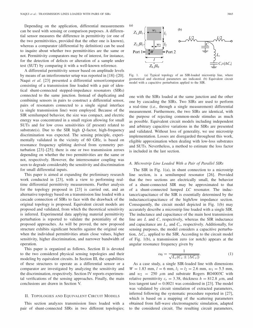
Fig. 1. (a) Typical topology of an SIR-loaded microstrip line, wheregeometrical and electrical parameters are indicated. (b) Equivalent circuitmodel with a capacitive perturbation applied to the SIR.
one with the SIRs loaded at the same junction and the otherone by cascading the SIRs. Two SIRs are used to performa real-time (i.e., through a single measurement) differentialmeasurement. Furthermore, the two SIRs are identical, withthe purpose of rejecting common-mode stimulus as muchas possible. Equivalent circuit models including independentand arbitrary capacitive variations in the SIRs are presentedand validated. Without loss of generality, we use microstripimplementation. Losses are disregarded throughout this work,eligible approximation when dealing with low-loss substratesand SUTs. Nevertheless, a method to estimate the loss factoris included in the last section.
A. Microstrip Line Loaded With a Pair of Parallel SIRs
The SIR in Fig. 1(a), in shunt connection to a microstripline section, is a semilumped resonator [26]. Providedthat the two sections are electrically small, the behaviorof a shunt-connected SIR may be approximated to thatof a shunt-connected lumped LC resonator. The induc-tance/capacitance of the SIR is essentially determined by theinductance/capacitance of the high/low impedance section.Consequently, the circuit model depicted in Fig. 1(b) mayaccurately describe a microstrip line loaded with a single SIR.The inductance and capacitance of the main host transmissionline are L and C , respectively, whereas the SIR inductanceand capacitance are Ls and Cs , respectively. Additionally, forsensing purposes, the model considers a capacitive perturba-tion, �Cs , applied to the SIR. According to the circuit modelof Fig. 1(b), a transmission zero (or notch) appears at theangular resonance frequency given by
ω0 = 1√Ls(Cs ± |�Cs |) . (1)
As a case study, a single SIR-loaded line with dimensionsW = 1.83 mm, l = 6 mm, l1 = l2 = 2.6 mm, w1 = 5.5 mm,and w2 = 250 μm and substrate Rogers RO4003C withrelative permittivity εr = 3.38, thickness h = 812.8 μm, andloss tangent tanδ = 0.0021 was considered in [23]. The modelwas validated by circuit simulation of extracted parameters,inferred following the systematic procedure reported in [27],which is based on a mapping of the scattering parametersobtained from full-wave electromagnetic simulation, adaptedto the considered circuit. The resulting circuit parameters,

3866 IEEE TRANSACTIONS ON MICROWAVE THEORY AND TECHNIQUES, VOL. 64, NO. 11, NOVEMBER 2016
Fig. 2. (a) Microstrip line loaded with a pair of identical SIRs at the samejunction and on opposite sides. (b) Equivalent circuit model with arbitrarycapacitive perturbations in the two SIRs. (c) Transformed equivalent circuitmodel. (d) Transformed and simplified equivalent circuit model with balancedperturbations.
characteristic impedances, and electrical lengths were found tobe Z0 = 50 �, Z1 = 23 �, and Z2 = 120 �; electrical lengthsat f0 = 3.83 GHz were βl0 = 45°, βl1 = 21°, and βl2 = 18°;and the circuit elements were L = 1.81 nH, C = 0.57 pF,Ls = 2.45 nH, and Cs = 0.70 pF (�Cs = 0).
To verify the modeling of an alteration in the resonatorcapacitance, a shape perturbation was produced in [23].Namely, the length of the wide section of the referenceresonator was enlarged (+|�l1|) or shortened (−|�l1|), with�l1 = ±0.5 mm = ±0.19l1, to increase (+|�Cs|) ordecrease (−|�Cs |) its associated capacitance, respectively.The circuit values of these perturbations (±|�Cs|), with�Cs = ±0.11 pF = ±0.15Cs , were obtained from (1)and the transmission zero frequencies were inferred fromelectromagnetic simulations. The transmission coefficient ofthese structures confirmed that the circuit simulations werein good accordance with those inferred from electromagneticsolvers in [23].
As expected from (1), any capacitive perturbation maybe sensed by monitoring the change in the resonance fre-quency. However, a real-time differential measurement of twocapacitive perturbations cannot be performed by loading atransmission line with a single SIR. Therefore, transmissionlines loaded with pairs of SIRs are necessary.
Fig. 2(a) shows a microstrip line loaded with a pair ofidentical shunt-connected SIRs placed at the same junction,and on opposite sides of the line (parallel configuration).In this topology, as was already considered in [23], it isassumed that both resonators are individually and simulta-neously capacitively perturbed by �Csi (i = 1, 2). Thelumped element equivalent circuit model that was proposedin [23] is shown in Fig. 2(b). The SIRs are close together, and
magnetic coupling between them is modeled, such a couplingbeing negative since the currents in the mirrored SIRs flowin opposite directions (i.e., the currents are antiparallel at thejunction of the SIRs). This coupling is accounted for by themutual inductance −|M|, the magnetic coupling coefficientbeing [26]
km = −|M|Ls
. (2)
From the equivalent T-circuit model of a two-port networkconsisting of a pair of coupled inductors, the circuit modelshown in Fig. 2(c) is inferred. If the capacitive perturbationsare identical (�Cs1 = �Cs2 = �Cs ), the simpler circuitdepicted in Fig. 2(d) results.
In balanced (i.e., identical) perturbations, according to thecircuit of Fig. 2(d), it can be readily noticed that the structureexhibits a single transmission zero at
ωe = 1√(Ls − |M|)(Cs ± |�Cs |) = ω0√
1 − |km | . (3)
In the presence of coupling, the transmission zero simply shiftsupward. The resonance frequency in (3) is denoted by ωe,in agreement to the nomenclature used in [26] to emphasizethe presence of an open circuit, under even mode excitation,at the symmetry plane of two identical coupled resonators.
In the case with different perturbations (�Cs1 �= �Cs2), thesymmetry in the shunt branch of the circuit model is disrupted.Although the resulting circuit model is not as simple as withbalanced perturbations, the resonance condition can be easilyobtained by setting the shunt branch impedance to zero. Thisgives the resonance frequencies of a circuit network composedof two magnetically coupled resonators, given by [26]
ωl,u =√√√√
Ls(Cs1+ Cs2)±√[Ls(Cs1 − Cs2)]2+ 4Cs1Cs2M2
2Cs1Cs2(
L2s − M2
)
(4)
where ωl and ωu denote the lower and upper resonancefrequencies, respectively. Therefore, a jump discontinuityarises due to unbalanced perturbations, giving rise to two splitresonance frequencies. The most relevant aspect is the factthat, because of coupling, the two resonances depend on thetwo perturbations, i.e., ωl,u = f (�Cs1,�Cs2). Accordingly,each resonance frequency cannot be independently tuned byits corresponding perturbation. In other words, when one ofthe resonators is perturbed, the two resonance frequencieschange (the more similar the perturbations, the higher thecross-dependence). It turns out that a parallel combination ofshunt-connected SIRs can be viewed as a dual-mode trisection(wide–narrow–wide) SIR [28]–[32], where symmetry disrup-tion is necessary to invoke the dual-mode behavior [33]. Notethat multimode resonators are usually utilized to reduce thesize of circuits, but in this paper, a dual resonant behavior isused to conduct a differential measurement.
To demonstrate the validity and usefulness of the modelsin Fig. 2, in [23], three different pairs of SIRs loading amicrostrip line were considered, as can be seen in Fig. 3(a):a symmetric pair, an asymmetric pair derived by increasing l1

NAQUI et al.: TRANSMISSION LINES LOADED WITH PAIRS OF SIRs 3867
Fig. 3. (a) Photograph of the considered microstrip lines loaded with pairsof parallel SIRs. The lower SIR is perturbed by ±|�Cs2|, whereas the upperSIR is unperturbed (�Cs1 = 0). The dimensions and substrate are thoseindicated in the text in reference to the single SIR-loaded line of [23] (exceptl = 15.9 mm to solder the connectors). (b) Magnitude of the transmissioncoefficient obtained from lossless electromagnetic and circuit simulations, andmeasurements. The circuit parameters are those indicated in the text for thesingle SIR-loaded line of [23], with M = −0.31 nH (km = −0.13), as theadditional host line length produces a phase shift only. The indicated resonancefrequencies correspond to those obtained by simulation.
in one of the SIRs (+|�Cs2|), and another asymmetric pairderived by decreasing l1 (−|�Cs2|). These structures werealready fabricated (using a drilling machine) and measuredin [23], but some fabrication-related tolerances and uncer-tainties were observed. For this reason, we have fabricatedthem again (using a photoetching process) to fit better themeasurements with the simulations. As the structures con-sidered are built up from those of single SIR loaded line,the only circuit parameter that needs to be obtained is themutual inductance. This parameter has been obtained by curvefitting the circuit simulation to the electromagnetic simulationin the case of the host line loaded with symmetric SIRs.Analytically, (3) can be used alternatively. The extracted valueis M = −0.31 nH (km = −0.13). As shown in Fig. 3(b), thecircuit simulations are consistent with both electromagneticsimulations and measurements, verifying that loss omission isa reasonable approximation using low-loss substrates.
It should be noted from Fig. 3 that the resonance frequencyat fu resembles that at fe, while an additional narrowband
Fig. 4. (a) Microstrip line loaded with a pair of identical SIRs incascade connection. (b) Equivalent hybrid circuit/TL model including arbitrarycapacitive perturbations. (c) Simplified equivalent circuit model when theresonators are spaced half-wavelength apart, i.e., the in-between transmissionline section has an electrical length of βls = 180°. (d) Simplified equivalentcircuit model for βls = 180° in the case of balanced perturbations.
lower resonance frequency at fl appears. When symmetry(with regard to the line axis) is broken, the bandwidth atfl is narrower than that at fu . The smaller the difference inthe perturbations, the narrower the lower notch. As a result,the discrimination to detect small differences between theperturbations is expected to be degraded by losses.
B. Microstrip Line Loaded With a Pair of Cascaded SIRs
This section deals with an alternative topology presentedin this paper to perform differential capacitive measurementsin such a way that interresonator coupling is prevented. Theproposed topology is illustrated in Fig. 4(a), and consists ofa transmission line loaded with a cascade connection of twoidentical SIRs that are spaced apart by a transmission linesection of length ls . If the SIRs are loaded on the sameside of the line, as is considered, the resonators may becoupled not only magnetically, but also electrically. However,the resonators are sufficiently separated so that we may assumethat the total coupling is negligible.
The proposed circuit model is shown in Fig. 4(b). Regard-less of the length of the transmission line section betweenresonators ls , the transmission zero frequencies are given by
ωl = min
(1√
Ls(Cs ± |�Cs1|) ,1√
Ls(Cs ± |�Cs2|))
(5a)
ωu = max
(1√
Ls(Cs ± |�Cs1|) ,1√
Ls(Cs ± |�Cs2|))
(5b)
where ωl and ωu denote again the lower and upper res-onance frequencies, respectively. According to the previousexpressions, the two resonances can be shifted independentlylike using single SIRs, even for unbalanced perturbations.

3868 IEEE TRANSACTIONS ON MICROWAVE THEORY AND TECHNIQUES, VOL. 64, NO. 11, NOVEMBER 2016
Clearly, the resonance frequency splitting phenomenon, whichemerges from unbalanced perturbations, is of different naturein the two configurations under study. In cascaded SIRs,splitting occurs as a mere result of frequency shifting, whereasin parallel SIR, there is a combination of frequency shiftingand interresonator coupling.
Let us now assume the particular case where the in-betweentransmission line section is half-wavelength long (ls = λ/2,where λ is the guided wavelength). As the input impedanceof a load seen through a λ/2 line is unchanged, the circuitin Fig. 4(b) is equivalent to that shown in Fig. 4(c). Notethat the SIRs are virtually connected at the same junctionso that the structure behaves as if the SIRs were physicallylocated at the same junction (due to periodicity, this holdsat integer multiples of λ/2). Indeed, the latter circuit is theideal one, which we would like to implement. The problems toimplement this idealized circuit are: 1) in parallel SIRs, thereis interresonator coupling (Section II-B) and 2) in cascadedSIRs, ls = λ/2 is satisfied at one frequency only (thiscondition is designed to be satisfied at the resonance frequencyof the unperturbed resonators). However, the latter issue isnot dramatic, since the resonance frequencies in (5) do notdepend on the interresonator distance (as long as interresonatorcoupling can be ignored). Therefore, the resonance frequenciesof the model in Fig. 4(c) always coincide with those of themodel in Fig. 4(b).
The last simplification makes the assumption that the per-turbations are identical (ωl = ωu = ω0). In this circumstance,the circuit in Fig. 4(c) derives to the one in Fig. 4(d),which is formally identical to that with parallel SIRs depictedin Fig. 2(d).
To demonstrate the usefulness of the cascaded approach,we have considered the same three previous scenarios in linewith the parallel connection [see Fig. 5(a)]. Accordingly, thesame circuit elements have been used to validate the equivalentcircuit models. As can be seen in Fig. 5(b), the agree-ment between the circuit/TL simulations, the electromagneticsimulations, and measurements is quite good. It deservesmentioning that a small ripple can be noticed from measure-ments in the symmetric structure, owing to the fact that thein-between transmission line is not exactly half-wavelength atthe corresponding resonance frequency. Importantly, the notchfrequencies are the same as those using single SIRs. Anotherrelevant result is that the bandwidth of both notches is notnarrow by nature, in contrast to what occurs at the lowerresonance frequency employing parallel SIRs.
C. Comparison Between the Topologies
To end this section, we compare the transmission zerofrequencies given by the two considered configurations,namely, those depicted in Figs. 3(a) and 5(a).
The results for the three considered scenarios with differentperturbations [Figs. 3(b) and 5(b), as well as the single SIR]are plotted in Fig. 6 for comparison purposes. From thisfigure, it is clear that the two concerning topologies manifest astrongly different behavior caused by the presence or absenceof interresonator coupling.
Fig. 5. (a) Photograph of the considered microstrip lines loaded with pairsof cascaded SIRs. The right SIR is perturbed by ±|�Cs2|, whereas theleft SIR is unperturbed (�Cs1 = 0). The dimensions, substrate, and circuitparameters are those of the single SIR-loaded line (except ls = 23.9 mm andl = 35.9 mm). (b) Transmission coefficient magnitude obtained from losslesselectromagnetic and circuit/TL simulations, and measurements. The indicatedresonance frequencies correspond to simulations.
Fig. 7 plots the resonance frequencies predicted by (3)–(5)in the case where a capacitive perturbation is applied to one ofthe SIRs (�Cs1 = 0 and �Cs2 �= 0). The considered circuitparameters of the unperturbed structures are those obtainedpreviously. Additionally, the resonances for the particularperturbed structures are also mapped to the curves. It isespecially visible that, when one of the resonators is perturbed(�Cs2 �= 0), the frequency splitting in parallel SIRs is charac-terized by a shift in the two resonances. On the contrary, forcascaded SIRs, only the resonance frequency of the perturbedresonator is shifted.
In conclusion, it can be drawn that a cascade connection ofSIRs provides a good solution to prevent coupling betweenthem. Moreover, significant advantages arise, particularly,

NAQUI et al.: TRANSMISSION LINES LOADED WITH PAIRS OF SIRs 3869
Fig. 6. Transmission coefficient magnitude (lossless electromagneticsimulation) of the considered microstrip lines loaded with parallel or cascadedSIRs for �Cs1 = 0, and (a) �Cs2 = 0, (b) +|�Cs2|, and (c) −|�Cs2|. Forcomparison purposes, the response using a single SIR [23] applying it to�Cs2 is also plotted.
Fig. 7. Resonance frequencies predicted by (3)–(5) versus a capacitiveperturbation (�Cs1 = 0 and −0.6 ≤ �Cs2/Cs ≤ 0.6) for the consideredreference microstrip lines loaded with parallel and cascaded SIRs, respectively.The circuit parameters of the reference structures are: L = 1.81 nH,C = 0.57 pF, Ls = 2.45 nH, Cs = 0.70 pF, and M = −0.31 nH. Theresonance frequencies of the three basic scenarios of Figs. 3 and 5, whichcorrespond to particular perturbations, are mapped.
the resonances are independent to each other (enhancing thesensitivity, as will be shown in Section III-C), their bandwidthis moderately wide by nature (improving the discrimination),the spectral separation between the resonance frequencies isnot enhanced by coupling (requiring a narrower bandwidthof operation), and unknown perturbations can be physicallyidentified. As will be shown, these advantages hold as long asthe perturbations are similar.
III. SENSITIVITY ANALYSIS
Thus far, capacitive perturbations have been produced bychanging the physical dimensions of the resonators. Evidently,in practice, the capacitive perturbations in a permittivity sensormust be due to permittivity perturbations of SUTs. We use
the term sample in order not to lose generality, meaning thatthe sample can be a material, liquid, organic tissue, and soforth. Furthermore, the SUT may also refer to a functionallayer that enhances the measurand-to-permittivity relationshipfor sensing purposes (e.g., in environmental sensors based onfunctional layers, a material highly sensitive to the environ-mental factor of interest is used).
This section evaluates the sensitivity in differentialpermittivity measurements, for both capacitive and permit-tivity perturbations. The study is conducted on the basis ofthe proposed equivalent circuit models, together with ana-lytical expressions of capacitances, and on electromagneticsimulations.
A. Analytical Sensitivity in Terms of Capacitance
With a view to performing differential sensing ofcapacitances in the considered approach based on frequencysplitting, the differential input is the difference between thecapacitances, that is,
Csd = Cs2 − Cs1. (6)
The output electrical variable to be monitored is frequency, andthe differential output is defined as the difference between theupper and lower resonance frequencies, that is,
fd = fu − fl . (7)
Obviously, despite the fact that the resonance for balancedperturbations is denoted by fe or f0, when a single resonanceis monitored, implicitly results fl = fu . The curve that relatesthe output and input quantities, namely fd(Csd), is namedtransfer function, whose slope is the sensitivity. Hence, thesensitivity is defined as the variation in the difference betweenthe resonance frequencies divided by the variation in the differ-ence between the capacitances. Mathematically, the sensitivitycan be written as
S = d fd
dCsd= lim
�Cs2−�Cs1→0
� fu − � fl
�Cs2 − �Cs1(8)
where �Csi (i = 1, 2) and � fl,u stand for individualincremental/decremental changes in capacitance and resonancefrequency, respectively. For simplicity, if one of the SIRs is notperturbed and considered to be a reference (so that �Cs1 = 0),then (8) reduces to
S = d fd
dCs2= lim
�Cs2→0
�( fu − fl )
�Cs2. (9)
In addition, in the cascade configuration, the magnitude of theanalytical sensitivity for null perturbation (y-axis) becomes
|S| = f0
2Cs2. (10)
The sensitivity should be as high as possible, and constantvalues of it are preferred. To gain insight into the sensitivity,instead of analyzing (9), which is cumbersome when theresonance frequencies are governed by (4), numerical solu-tions will be given. The resonance frequencies determinedby (3) and (4) for two different coupling coefficients and by (5)are plotted in Fig. 8(a) assuming �Cs1 = 0. It is evident that

3870 IEEE TRANSACTIONS ON MICROWAVE THEORY AND TECHNIQUES, VOL. 64, NO. 11, NOVEMBER 2016
Fig. 8. (a) Resonance frequencies given by (3) and (4) for different kmand (5) normalized to the constant resonance frequency of the nonperturbeduncoupled SIR determined by (5). The capacitive perturbations are �Cs1 = 0and −0.6 ≤ �Cs2/Cs ≤ 0.6. (b) Normalized transfer function. (c) Sensitivitymagnitude normalized to the case of balanced perturbations (�Cs2 = 0) in thecascaded configuration. For the parallel arrangement, sensitivity is calculatedusing (4) solely, disregarding (3) in order not to calculate the sensitivity acrossthe jump discontinuity.
the output is null in the case of a perfect balance of pertur-bations (�Cs1 = �Cs2 = 0). On the other hand, unbalancedperturbations have been introduced by a capacitive variationin one of the SIRs (�Cs1 = 0, �Cs2 �= 0). As expected, whenkm �= 0, corresponding to the case with parallel SIRs, fu ismore sensitive to −|�Cs2| than fl , and complementarily,fl is more sensitive to +|�Cs2|. Both frequencies tend tothe frequencies without coupling as the capacitive perturbationincreases.
Fig. 8(b) shows the corresponding transfer function fromwhich it is apparent that, as |km | increases, the frequency
splitting, fd , strengthens. It turns out that the sensitivity,shown in Fig. 8(c), worsens as |km| increases. Indeed, themaximum sensitivity corresponds to the case of (uncoupled)cascaded SIRs, and is given by (10). Specifically, a significantdegradation in the sensitivity results in small perturbations.As was stressed earlier, even for loose coupling coefficients,coupling cannot be neglected for similar perturbations. Nev-ertheless, the parallel configuration can be useful when theperturbations differ from each other significantly. In thesesituations, coupling plays an insignificant role.
The results in Fig. 8 were already published in [23],where using parallel SIRs with km = 0 was assumed tobe fictitious. Here, km = 0 is no longer fictitious, as itis implemented employing cascaded SIRs. For small inputs,since the interresonator coupling in parallel SIRs decreases thesensitivity, parallel-connected SIRs are apparently not muchappropriate to properly operate as a sensor. In addition, thistopology working as a comparator between two capacitivelyperturbed SIRs is not very promising. As mentioned before,the discrimination for small differential inputs is expectedto be rather limited due to the narrowband nature of thelower resonance. Conversely, SIRs in cascade connection areexpected to achieve high sensitivities and discriminations.
It should be mentioned that the dynamic range of measure-ment is not limited to the considered one (|�Cs2| ≤ 0.6Cs ).This relatively small dynamic range, however, allows forillustrating properly the handicap of the parallel configuration,i.e., low performance under small inputs. Finally, it is alsoimportant to highlight that the sensitivity is not constant dueto the fact that the transfer function is not linear [this isindeed evident from the simplest form of the sensitivity givenby (10)]. Moreover, sensitivity is not a symmetric functionwith respect to the y-axis, i.e., S (+|�Csd|) �= S(−|�Csd|).Instead, the sensitivity magnitude increases or decreases as theinput capacitance is increasingly lower or higher, respectively.
B. Analytical Sensitivity in Terms of Permittivity
In Section III-A, we considered a capacitive input as ageneralization. Capacitive variations can be produced by sev-eral means, e.g., by changing the physical dimensions of theresonators (i.e., shape perturbation as done in Section II) or bychanging dielectric properties (i.e., material perturbation, as itmust be in practice). Therefore, in a real sensor the differentialinput is the difference in the relative permittivity of the SUTs,defined here as
εrd = εr2 − εr1. (11)
It should be noted that the sensor measures the differencebetween two permittivities. If one of the two permittivitiesis known, the other permittivity can be inferred.
The sensitivity in terms of relative permittivity becomes
S = ∂ fd
∂εrd= lim
�εr2−�εr1→0
� fu − � fl
�εr2 − �εr1(12)
where �εri (i = 1, 2) stands for changes in relative permittiv-ity. The partial derivatives indicate that the output differentialfrequency may be influenced by other physical variables
NAQUI et al.: TRANSMISSION LINES LOADED WITH PAIRS OF SIRs 3871
related to cross sensitivities, as will be illustrated further in thissection. By assuming a linear dependence of the capacitancewith the permittivity (with proportionality constant k), andletting �εr1 = 0 and km = 0 once again, the sensitivitymagnitude becomes
|S| = f0
2εr2. (13)
To analytically establish the transfer function and sensitivityabove, the SIR capacitance was approximated by the parallel-plate capacitance of its wide section, namely,
Cp = ε0εr2w1l1
h= kεr2 (14)
where ε0 is the vacuum permittivity. In (14), the substrate inthe vicinity of the wide section is supposed to be replacedwith one SUT. The most relevant aspect in this approximationis that the SIR capacitance is linearly dependent on thepermittivity. The corresponding capacitance for the referenceSIR is Cp = 0.53 pF. However, (14) must be consideredas a first-order approximation as mentioned above, wherel1, w1 � h are required for accurate results. Likewise, Cs isneither exactly proportional to l1; �l1 = ±0.19l1 produces�Cs = ±0.15Cs .
Finally, to illustrate the robustness of differentialmeasurements against cross sensitivities, let us assume thatwe compare two identical materials (�Cs = �Cs1 = �Cs2).Using a two-step process with a single SIR, the resultingresonance frequencies are
ω0 = 1√Ls(Cs + �Cs)
. (15)
Let us now introduce a spurious change in the capacitancerelated to a cross sensitivity, denoted by �Cxi (i = 1, 2).As the effect of cross sensitivities may change over time, onemay assume �Cx1 �= �Cx2 (neither a compensation techniquenor recalibration is considered). Hence, in the presence ofcross sensitivities, the different drifts shift the resonancefrequencies to
ω01 = 1√Ls(Cs + �Cs + �Cx1)
(16a)
ω02 = 1√Ls(Cs + �Cs + �Cx2)
. (16b)
Therefore, fd �= 0 and the readout is going to be wrong.By contrast, performing the proposed real-time differentialmeasurement, using the cascaded configuration, the resultingsingle resonance frequency is
ωl = ωu = ω0 = 1√Ls(Cs + �Cs)
. (17)
Since the two materials are the same and affected by crosssensitivities at the same time, it is reasonable to assume that�Cx = �Cx1 = �Cx2, so that
ωl = ωu = ω0 = 1√Ls(Cs + �Cs + �Cx )
. (18)
Consequently, fd = 0, indicating that there is no differencebetween the materials. Note, however, that a comparison
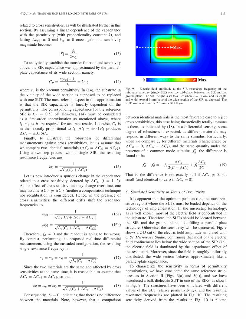
Fig. 9. Electric field amplitude at the SIR resonance frequency of thereference structure (single SIR) over the mid-plane between the SIR and theground plane. The SUT height is set to h−2t where t = 35 μm, and its lengthand width extend 1 mm beyond the wide section of the SIR, as depicted. TheSUT size is 4.6 mm × 7.5 mm × 812.8 μm.
between identical materials is the most favorable case to rejectcross sensitivities, this case being theoretically totally immuneto them, as indicated by (18). In a differential sensing, somedegree of robustness is expected, as different materials mayrespond in different ways to the same stimulus. Particularly,when we compare fd for different materials (characterized by�Cs1 = 0, �Cs2 = �Cs), and the same quantity under thepresence of a common mode stimulus f ′
d , the difference isfound to be
f ′d − fd = − fu
�Cx
2(C + �Cs)+ fl
�Cx
2C. (19)
That is, the difference is not exactly null if �Cx �= 0, butsmall (and identical to zero if �Cs = 0).
C. Simulated Sensitivity in Terms of Permittivity
It is apparent that the optimum position (i.e., the most sen-sitive region) where the SUTs must be loaded depends on thetechnology of implementation. In the microstrip technology,as is well known, most of the electric field is concentrated inthe substrate. Therefore, the SUTs should be located betweenthe SIR and the ground plane, like filling a parallel-platestructure. Otherwise, the sensitivity will be decreased. Fig. 9shows a 2-D cut of the electric field amplitude simulated withC ST Microwave Studio, confirming that most of the electricfield confinement lies below the wide section of the SIR (i.e.,the electric field is dominated by the capacitance effect ofthe resonator). Moreover, since the field is roughly uniformlydistributed, the wide section behaves approximately like aparallel-plate capacitance.
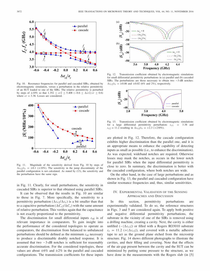
To characterize the sensitivity in terms of permittivityperturbations, we have considered the same reference struc-tures as in Section II [Figs. 3(a) and 5(a)], and we haveintroduced a bulk dielectric SUT in one of the SIRs, as shownin Fig. 9. The structures have been simulated with differentvalues of the SUT relative permittivity εr2, and the resultingresonance frequencies are plotted in Fig. 10. The resultingsensitivity derived from the results in Fig. 10 is plotted
3872 IEEE TRANSACTIONS ON MICROWAVE THEORY AND TECHNIQUES, VOL. 64, NO. 11, NOVEMBER 2016
Fig. 10. Resonance frequencies for parallel and cascaded SIRs, obtained byelectromagnetic simulation, versus a perturbation in the relative permittivityof an SUT loaded to one of the SIRs. The relative permittivity is perturbedby steps of ±10% so that 1.352 ≤ εr2 ≤ 5.408 (−0.6 ≤ �εr2/εr ≤ 0.6)where εr = 3.38. Losses are considered.
Fig. 11. Magnitude of the sensitivity derived from Fig. 10 by steps of�εr2/εr = ±0.1 (±10%). The sensitivity in the jump discontinuity of theparallel configuration is not calculated. As stated by (13), the sensitivity andthe perturbation have the same sign.
in Fig. 11. Clearly, for small perturbations, the sensitivity incascaded SIRs is superior to that obtained using parallel SIRs.
It can be observed that the results in Fig. 10 are similarto those in Fig. 7. More specifically, the sensitivity to apermittivity perturbation (�εr2/�εr ) is a bit smaller than thatto a capacitive perturbation (�Cs2/�Cs ) with the same amountof relative perturbation. This verifies again that the capacitanceis not exactly proportional to the permittivity.
The discrimination for small differential inputs εrd is ofrelevant importance in comparators. To gain insight intothe performance of the considered topologies to operate ascomparators, the discrimination from balanced to unbalancedperturbations should be defined as the minimum εrd necessaryto produce a discriminable doubly notched response. It isassumed that two −3-dB notches is sufficient for reasonablyaccurate discrimination. For the considered topologies, thesevalues are about ±6% and ±2% in the parallel and cascadedconfigurations. The transmission coefficients for these inputs
Fig. 12. Transmission coefficient obtained by electromagnetic simulationsfor small differential permittivity perturbations in (a) parallel and (b) cascadedSIRs. The perturbations are those necessary to obtain two −3-dB notches:�εr2/εr = ±0.06 and ±0.02 (6% and 2%), respectively.
Fig. 13. Transmission coefficient obtained by electromagnetic simulationsfor a large differential permittivity perturbation: εr1 = 3.38 andεr2 = 11.2 resulting in �εr2/εr = +2.3 (+230%).
are plotted in Fig. 12. Therefore, the cascade configurationexhibits higher discrimination than the parallel one, and it isan appropriate means to enhance the capability of detectinginputs as small as possible (i.e., to enhance the discrimination).As was expected, wideband notches are required. Otherwiselosses may mask the notches, as occurs in the lower notchfor parallel SIRs when the input differential permittivity isclose to zero. In summary, the discrimination is better withthe cascaded configuration, where both notches are wide.
On the other hand, in the case of large perturbations and asshown in Fig. 13, the parallel and cascaded configuration havesimilar resonance frequencies and, thus, similar sensitivities.
IV. EXPERIMENTAL VALIDATION OF THE SENSING
APPROACHES AND DISCUSSION
In this section, permittivity perturbations areexperimentally validated. To do so, the reference structuresin Figs. 3 and 5 are considered again. To apply both positiveand negative differential permittivity perturbations, thesubstrate in the vicinity of one of the SIRs is removed usinga drilling machine, creating a cavity. Next, the cavity is eitherunfilled (−|�εr2|) or filled with a Rogers RO3010 substrateεr = 11.2 (+|�εr2|), and covered with a metallic adhesivetape to act as the ground plane etched from the microstripstructure. Fig. 14 shows different photographs to illustrate thecavities, and their filling and covering. Note that the effectsof the air-gap present between the cavity and the SUT can beminimized by putting some pressure to the structure, as wehave done in the measurements with the Rogers slab (in [5]

NAQUI et al.: TRANSMISSION LINES LOADED WITH PAIRS OF SIRs 3873
Fig. 14. Photographs of the reference structures composed of microstriplines loaded with pairs of (a) parallel and (b) cascaded SIRs. From left toright: 1) cavity in one of the SIRs; 2) filled cavity with Rogers RO3010 withεr2 = 11.2; and 3) cavity covered with a metallic tape. (c) Photograph of theexperimental setup for measurement, including the Agilent N5221A networkanalyzer, cables, connectors, and sensing system.
a systematic method to eliminate the effects of the air gapis reported).
A. Determining the Dielectric Constant of the SUT
The measured results of the positive/negative perturbations,plotted in Fig. 15, together with those with no perturbation,are in accordance with theory. Even though the cavity dimen-sions cannot be controlled very accurately with the in-housedrilling, these experiments validate the sensing principle underpermittivity perturbation. Nevertheless, inspection of Fig. 15reveals that the difference in notch frequencies is somehowsmaller than the results of Fig. 10 for the considered dielectricconstant values (1 for the unfilled cavity, and 11.2 for the filledcavity with the considered Rogers material). The reason is thatthe cavity has been implemented by milling, and we have notcompletely removed all the substrate material, since the SIRneeds some material for mechanical stability. Therefore, theunfilled cavity, including the remaining substrate layer, hasan effective dielectric constant larger than 1, and the cavityfilled with the Rogers substrate (dielectric constant 11.2) hasactually an effective dielectric constant smaller than 11.2.
Fig. 15. Measured transmission coefficient magnitude for the (a) paral-lel and (b) cascaded topologies under dielectric loading. Three scenariosare considered: 1) without cavity (�εr2 = 0); 2) unfilled cavity so thatεr2 = 1 (−|�εr2 |); and 3) filled cavity with Rogers RO3010 withεr2 = 11.2 (+|�εr2|). No perturbation is applied to the other SIR (�εr1 = 0).
In other words, the measurement provides the effective dielec-tric constant of the structure below the SIR, including notonly the SUT but also the presence of a narrow dielectriclayer of relative permittivity of 3.38. Moreover, the thicknessof the whole structure, layer on top the cavity plus SUT, isnot necessarily the same as the thickness of the substrate.In the simulations that have been carried out to obtain theresults of Fig. 10, we have not considered this substrate layerbetween the SIR metal level and the SUT. In practice, it isvery difficult for us to precisely control the thickness of theremaining substrate between the SIR patch and the cavity. Forthis main reason, such a layer has not been considered inthe simulations. However, note that with a more sophisticatedfabrication technology (e.g., micromachining), such controlwould not be a problem.
Nevertheless, we have proposed a method to determine thisthickness that subsequently allows us to obtain the dielectricconstant of the SUT once the reference permittivity (the one ofthe substrate, i.e., εr1) and the thickness of the SUT are known.Let us consider that h1 and hc are the thicknesses of thesubstrate layer on top of the cavity and the cavity, respectively,so that h1 + hc = h, the substrate thickness. Moreover let usassume that the SUT corresponds to a material with well-known dielectric constant εr2 and thickness h2 (see Fig. 16).The method is based on the fact that the effective dielectricconstant of the composite formed by the substrate layer on thetop of the cavity plus the SUT εeff is related to the respectivedielectric constants by
εeff
h=
εr1h1
· εr2h2
εr1h1
+ εr2h2
. (20)
From the previous expression, the dielectric constant of theSUT can be isolated
εr2 = εeffεr1h2
εr1h − εeffh1(21)

3874 IEEE TRANSACTIONS ON MICROWAVE THEORY AND TECHNIQUES, VOL. 64, NO. 11, NOVEMBER 2016
Fig. 16. Sketch (not drawn to scale) of the top and cross-sectional view ofthe SIR and cavity loaded with the SUT.
Fig. 17. Measured transmission coefficient magnitude for the cascadedtopology with the cavity filled by an Arlon substrate with characteristicsindicated in the text.
where εeff can be inferred from the split in frequency of theSUT and the curve of Fig. 10 corresponding to the cascadeconnection. Thus, if εr2 and h2 are known, h1 can be obtainedfrom (21). For the SUT corresponding to the Rogers substratewith εr2 = 11.2 and h2 = 635 μm, and considering that thenotch frequencies of Fig. 15(b) provide εeff = 4.9, accordingto Fig. 10, the resulting thickness of the layer on top of thecavity is found to be h1 = 369 μm. To verify the validityof this result, we have considered the curve of Fig. 15(b)corresponding to the unfilled cavity (εr2 = 1). By introducingthe corresponding effective dielectric constant εeff = 1.69in (21), and h1 = 369 μm, the air thickness is found to beh2 = 371 μm, which is in reasonable agreement with thethickness of the cavity (note, however, that the metallic tapeis somehow flexible and hence may reduce the effective valueof the cavity thickness).
Once h1 is known, we can calculate the dielectricconstant of another SUT, an Arlon slab with εr2 = 2.43 andh2 = 490 μm. The measured transmission coefficient for thecascaded configuration is depicted in Fig. 17. The effectivedielectric constant that results from Fig. 10 is εeff = 2.70, andusing (21), the dielectric permittivity is found to be εr2 = 2.50,very close to the nominal value (2.43).
It is interesting to analyze expression (21) and the depen-dence of the dielectric constant of the SUT with the differentparameters. Particularly, it linearly depends on the thicknessof the SUT, h2. Therefore, uncertainties in this parameter aredirectly translated into the dielectric constant. The dependence
on the other geometrical parameters h and h1 can be appreci-ated in expression (21) as well. The thickness of the substrateh is typically known with good accuracy. On the other hand,the dependence on h1 is modulated by εeff , and the effects ofthe uncertainty with this parameter are minimized in sampleswith small dielectric constant (and hence small εeff ). In viewof (21), and considering that εeff is roughly proportionalto εr1, namely,
εeff = εr1 + �εr2 = εr1 + � f
S≈ εr1 + 2εr1
� f
f0(22)
it follows that εr2 is proportional to εr1 [see (21)] and hencethe uncertainties in the dielectric constant of the referencematerial are (roughly) directly translated into the one of themeasured materials.
Comparison of the proposed differential sensor withother permittivity sensors based on microstrip technology,such as those sensors based on CSRRs [3]–[5], is not easy.Nevertheless, the fact that the proposed sensors are differ-ential represents advantages in several aspects. As compara-tors, common-mode stimuli are minimized by means of adifferential-mode approach, as discussed before, and smallchanges between two (apparently identical) samples can bedetected. Comparators based on this approach can be ofinterest to determine defects or abnormalities in a sample,compared with a well-known reference, as well as softpermittivity changes in circuits manufactured on microwavelaminates. In a real scenario, two identical cavities must bepresent, each one below the corresponding SIR patch.
Concerning sensitivity, the capacitance of the SIR isbroadside and hence very sensitive to the permittivity, com-pared to the case of edge capacitances (such as the one ofCSRRs). The sensitivity that can be inferred from the sensorsreported in [3]–[5] is very reasonable, but not as good as theone reported in this paper [of the order of 0.6 GHz for smallperturbations, according to Fig. 10 and expression (13)—notethat we have considered the relative permittivity, i.e., dimen-sionless, in the denominator of (13)]. Note that according toexpression (13), such sensitivity can be modulated by meansof the SIR dimensions, which provide the resonance frequencyfor the unperturbed state.
B. Loss Tangent Estimation
Even though this paper is focused on low-loss substratesand SUTs (as mentioned before), let us discuss a procedureto estimate the loss tangent. It is based on the depth ofthe notch (similar to [4] and [5]), and for this reason astructure with a single SIR is preferred (i.e., nondifferential).Otherwise, the presence of closed notches (as results in caseswith small differential permittivities) may obscure the results.The initial assumption is that the substrate material belowthe SIRs is completely removed and replaced with the SUT.Let us consider two causes of losses, i.e., metallic losses,mainly associated to the narrow inductive strip of the SIR, anddielectric losses, related to the SUT. The model of the SIR-loaded line with losses included is the one of Fig. 1(b), butincluding a resistance, RM , in series with the inductance Ls ,

NAQUI et al.: TRANSMISSION LINES LOADED WITH PAIRS OF SIRs 3875
plus a resistance, RD , parallel connected to the capacitance Cs .The impedance of this shunt branch is
Z in = RM + RD
1 + R2DC2
s ω2+ j
(
ωLs − R2DCsω
1 + R2DC2
s ω2
)
(23)
and this expression can be approximated by
Z in = RM + 1
RDC2s ω2 + j
(
ωLs − 1
Csω
)
(24)
where it has been assumed that R2DC2
s ω2 � 1, correspondingto SUTs with moderate or low-loss levels (note that in anideal lossless SUT, RD = ∞). At the notch frequency, thereactive part of Z in nulls, and the resulting resistance can beexpressed as
RLOSS = RM + 1
CsωQD(25)
where QD is the SUT quality factor. Such resistance is relatedto the magnitude of the transmission coefficient at the notchfrequency by
RLOSS = Z0|S21|2(1 − |S21|) (26)
and therefore it can be inferred from the measured frequencyresponse. On the other hand,
tan δ = 1
RDCsω= Q−1
D . (27)
If RM is known, (25) gives QD and hence tanδ can beinferred from (27). To determine the contribution of the metal-lic losses RM , a possible procedure is to consider a referenceSUT (or substrate) with a well-known tanδ (and hence QD).From (25), RM can be isolated, and used subsequently for thedetermination of the loss tangent of the SUT (it is assumedthat RM does not vary with the SUT).
The previous procedure cannot be directly applied in generalto our proof-of-concept cascaded SIR-based sensor since itis based on two SIRs, and, moreover, there is a remainingsubstrate layer on top of the cavity. However, for the con-sidered SUT, the Arlon slab with nominal permittivity andthickness εr2 = 2.43 and h2 = 490 μm, the frequencyresponse shows quite uncoupled notches and, therefore, we canmodify the procedure and at least make an estimation of thetanδ. By introducing the SUT into the cavity, expression (25)can be rewritten as
RLOSS = RM + 1
C1ωQ1+ 1
C2ωQ2(28)
where the subindex 1 and 2 refer to the layer on top of thecavity and SUT, respectively. By identifying the last two termswith the loss contribution of the composite (CeqωQeq)
−1,it follows that:
Qeq = (C1 + C2)Q1 Q2
Q1C1 + Q2C2. (29)
This expression depends on the ratio C2/C1, which canbe determined from the thickness of the layer and SUT andfrom the dielectric constants. Using (25) with Cs = Ceq and
QD = Qeq and with RLOSS inferred from (26), where S21is obtained from the depth of the second notch in Fig. 17,we can determine Qeq, which is found to be Qeq = 366.Since Q1 is known (Q1 = tan δ)−1 = 476, we can isolate Q2from (29), and the resulting value is found to be Q2 = 353,which gives tanδ = 0.0028 (in reasonable agreement withthe nominal value of 0.0020). Note that we cannot expect anaccurate value of the loss factor with the considered in-housemeasurement system, necessarily affected by additional lossessuch as those derived from the connectors, soldering, metallicadhesive tape, etc. Nevertheless, a procedure to estimate thetanδ of the SUT has been reported.
V. CONCLUSION
This paper analyzes two simple strategies to conductdifferential measurements of permittivity. These strategiesare based on loading pairs of SIRs, in either parallel orcascade connection, to a microstrip line. It has been shownthat, although the most canonical symmetric configurationto perform a differential measurement is the one wherethe SIRs are parallel-connected, such a structure exhibitslower performance for small differential permittivities dueto interresonator coupling, and hence the cascade connectionis preferred in these situations. The differential technique issimple, as a transmission line is driven with a single-endedRF/microwave signal, and the SIRs are simply simultaneouslyand individually loaded with dielectric materials. The sensingprinciple is based on resonance frequency splitting, so thatwhen the permittivities of the two dielectric materials areidentical the sensor exhibits a single resonance frequency,whereas two resonances are present if such permittivitiesare different. The sensing principle has been experimentallyvalidated by both shape and material perturbations. This mainfocus in this paper has been on the differential measurement.A method to determine the dielectric constant of a certainSUT, provided the one of the reference is known, has beenproposed. Finally, despite that the analysis of the presentwork has been carried out by excluding losses, a method toestimate the loss tangent of the SUT has been also reported.As is well known, changing environmental factors may changethe permittivity and, therefore, miscalibration. By virtue of adifferential measurement, sensing and comparison with somedegree of immunity to these external factors are expected.
REFERENCES
[1] E. Nyfor, “Industrial microwave sensors—A review,” Subsurf. Sens.Technol. Appl., vol. 1, no. 1, pp. 23–43, Jan. 2000.
[2] M. Tiuri, “Microwave sensor applications in industry,” in Proc. Eur.Microw. Conf., Sep. 1987, pp. 25–32.
[3] M. S. Boybay and O. M. Ramahi, “Material characterization using com-plementary split-ring resonators,” IEEE Trans. Instrum. Meas., vol. 61,no. 11, pp. 3039–3046, Nov. 2012.
[4] C.-S. Lee and C.-L. Yang, “Complementary split-ring resonators formeasuring dielectric constants and loss tangents,” IEEE Microw. WirelessCompon. Lett., vol. 24, no. 8, pp. 563–565, Aug. 2014.
[5] C.-L. Yang, C.-S. Lee, K.-W. Chen, and K.-Z. Chen, “Noncontactmeasurement of complex permittivity and thickness by using pla-nar resonators,” IEEE Trans. Microw. Theory Techn., vol. 64, no. 1,pp. 247–257, Jan. 2016.
[6] M. Puentes, C. Weiß, M. Schüßler, and R. Jakoby, “Sensor array basedon split ring resonators for analysis of organic tissues,” in IEEE MTT-SInt. Microw. Symp. Dig., Baltimore, MD, USA, Jun. 2011, pp. 1–4.

3876 IEEE TRANSACTIONS ON MICROWAVE THEORY AND TECHNIQUES, VOL. 64, NO. 11, NOVEMBER 2016
[7] M. Puentes, Planar Metamaterial Based Microwave Sensor Arrays forBiomedical Analysis and Treatment. Heidelberg, Germany: Springer,2014.
[8] T. Chretiennot, D. Dubuc, and K. Grenier, “A microwave and microflu-idic planar resonator for efficient and accurate complex permittivitycharacterization of aqueous solutions,” IEEE Trans. Microw. TheoryTechn., vol. 61, no. 2, pp. 972–978, Feb. 2013.
[9] A. A. Abduljabar, D. J. Rowe, A. Porch, and D. A. Barrow, “Novelmicrowave microfluidic sensor using a microstrip split-ring resonator,”IEEE Trans. Microw. Theory Techn., vol. 62, no. 3, pp. 679–688,Mar. 2014.
[10] A. Ebrahimi, W. Withayachumnankul, S. Al-Sarawi, and D. Abbott,“High-sensitivity metamaterial-inspired sensor for microfluidic dielectriccharacterization,” IEEE Sensors J., vol. 14, no. 5, pp. 1345–1351,May 2014.
[11] W. Withayachumnankul, K. Jaruwongrungsee, A. Tuantranont,C. Fumeaux, and D. Abbott, “Metamaterial-based microfluidic sensorfor dielectric characterization,” Sens. Actuators A, Phys., vol. 189,pp. 233–237, Jan. 2013.
[12] H.-J. Lee and J.-G. Yook, “Biosensing using split-ring resonators atmicrowave regime,” Appl. Phys. Lett., vol. 92, no. 25, p. 254103, 2008.
[13] K. Grenier et al., “Integrated broadband microwave and microfluidic sen-sor dedicated to bioengineering,” IEEE Trans. Microw. Theory Techn.,vol. 57, no. 12, pp. 3246–3253, Dec. 2009.
[14] T. Chen, D. Dubuc, and K. Grenier, “Resonant-based microwave biosen-sor for physiological liquid identification,” in Proc. Eur. Microw. Conf.,Amsterdam, The Netherland, Oct./Nov. 2012, pp. 448–450.
[15] T. Chretiennot, D. Dubuc, and K. Grenier, “Optimized electromagneticinteraction microwave resonator/microfluidic channel for enhanced liq-uid bio-sensor,” in Proc. Eur. Microw. Conf., Nuremberg, Germany,Oct. 2013, pp. 464–467.
[16] T. Chretiennot, D. Dubuc, and K. Grenier, “Double stub resonantbiosensor for glucose concentrations quantification of multiple aqueoussolutions,” in IEEE MTT-S Int. Microw. Symp. Dig., Tampa, FL, USA,Jun. 2014, pp. 1–4.
[17] E. Ekmekci and G. Turhan-Sayan, “Multi-functional metamaterial sen-sor based on a broad-side coupled SRR topology with a multi-layersubstrate,” Appl. Phys. A, Solids Surf., vol. 110, no. 1, pp. 189–197,Jan. 2013.
[18] C. Damm, M. Schüßler„ M. Puentes, H. Maune, M. Maasch, andR. Jakoby, “Artificial transmission lines for high sensitive microwavesensors,” in Proc. IEEE Sensors Conf., Christchurch, New Zealand,Oct. 2009, pp. 755–758.
[19] C. Damm, Artificial Transmission Line Structures for TunableMicrowave Components and Microwave Sensors. Aachen, Germany:Shaker Verlag, 2011.
[20] M. Schueler, C. Mandel, M. Puentes, and R. Jakoby, “Metamaterialinspired microwave sensors,” IEEE Microw. Mag., vol. 13, no. 2,pp. 57–68, Mar. 2012.
[21] J. G. Webster, The Measurement Instrumentation and Sensors Hand-book. Boca Raton, FL, USA: CRC, 1999.
[22] J. Fraden, Handbook of Modern Sensors: Physics, Design, and Appli-cations, 3rd ed. New York, NY, USA, Springer, 2004.
[23] J. Naqui, C. Damm, A. Wiens, R. Jakoby, L. Su, and F. Martin,“Transmission lines loaded with pairs of magnetically coupled steppedimpedance resonators: Modeling and application to microwave sensors,”in IEEE MTT-S Int. Microw. Symp. Dig., Tampa, FL, USA, Jun. 2014,pp. 1–4.
[24] J. Naqui, Symmetry Properties in Transmission Lines Loaded WithElectrically Small Resonators: Circuit Modeling and Applications. Hei-delberg, Germany: Springer, 2016.
[25] A. K. Horestani, J. Naqui, Z. Shaterian, D. Abbott, C. Fumeaux, andF. Martín, “Two-dimensional alignment and displacement sensor basedon movable broadside-coupled split ring resonators,” Sens. Actuators A,Phys., vol. 210, pp. 18–24, Apr. 2014.
[26] J.-S. Hong and M. J. Lancaster, Microstrip Filters for RF/MicrowaveApplications. New York, NY, USA: Wiley, 2001.
[27] J. Bonache, M. Gil, I. Gil, J. Garcia-Garcia, and F. Martin, “On theelectrical characteristics of complementary metamaterial resonators,”IEEE Microw. Wireless Compon. Lett., vol. 16, no. 10, pp. 543–545,Oct. 2006.
[28] R. Mongia, I. Bahl, and P. Bhartia, RF and Microwave Coupled LineCircuits. Norwood, MA, USA: Artech House, 1999.
[29] C. Cui and Y. Liu, “Quad-band bandpass filter design by embeddingdual-band bandpass filter with dual-mode notch elements,” Electron.Lett., vol. 50, no. 23, pp. 1719–1720, Nov. 2014.
[30] M. Makimoto and S. Yamashita, “Compact bandpass filters usingstepped impedance resonators,” Proc. IEEE, vol. 67, no. 1, pp. 16–19,Jan. 1979.
[31] D. Girbau, A. Lazaro, and R. Villarino, “Passive wireless permittivitysensor based on frequency-coded chipless RFID tags,” in IEEE MTT-SInt. Microw. Symp. Dig., Montreal, QC, Canada, Jun. 2012, pp. 1–4.
[32] J.-S. Hong, H. Shaman, and C. Y.-H. Chun, “Dual-mode microstripopen-loop resonators and filters,” IEEE Trans. Microw. Theory Techn.,vol. 55, no. 8, pp. 1764–1770, Aug. 2007.
[33] V. A. Fedotov, M. Rose, S. L. Prosvirnin, N. Papasimakis, andN. I. Zheludev, “Sharp trapped-mode resonances in planar metamaterialswith a broken structural symmetry,” Phys. Rev. Lett., vol. 99, no. 14,p. 47401, Oct. 2007.
Jordi Naqui (S’11–M’14) was born in Granollers,Spain. He received the diploma degree in Telecom-munication Technical Engineering (with a spe-cialization in electronic systems), the degree inTelecommunication Engineering, the master’s degreein Microelectronics and Nanoelectronics Engineer-ing, and the Ph.D. degree in electronics engineeringfrom the Universitat Autònoma de Barcelona (UAB),Barcelona, Spain, in 2006, 2010, 2011, and 2014,respectively.
From 2009 to 2016, he was with UAB, where hisresearch activities were focused on circuit modeling, filters, and sensors. From2010 to 2016, he taught with the Department of Electronics Engineering.Currently, he is a Senior Filter Design Engineer with Qorvo, Munich,Germany.
Mr. Naqui was a recipient of the Pre-Doctoral Fellowship by the SpanishGovernment. He was also a recipient of the Yarman-Carlin Best Student PaperContest of the 14th MMS, the Young Scientist Award at the XXX URSISpanish National Symposium, the IX Comerma Engineer Research Award bythe Local Government of Ferrol and the University of A Coruña, and the BestDoctorate Student Award.
Christian Damm (S’04–GS’09–M’09) was born inMarburg, Germany, in 1977. He received the Dr.-Ing. degree in theoretical electrical engineering fromthe Technische Universität Darmstadt, Darmstadt,Germany, in 2010.
Since 2014, he has been a Full Professor andthe Head of the Terahertz Sensors Group, Technis-che Universität Darmstadt. His research has beenfocused on transmission line metamaterials and tun-able metamaterials for microwave applications suchas phase shifters, matching networks, and leaky
wave antennas. He developed a strong involvement in the material char-acterization of artificial materials and liquid crystals as enabling materialfor tunable metamaterials. Recently, the frequency range for his researchactivities has been extended to the terahertz regime. He is currently involvedin the coordination and research activities of the German Priority Program“ESSENCE” SPP1857, focused on the life science applications of electro-magnetic sensors. His current research interests include sensor applicationsbased on metamaterials and periodic structures.
Mr. Damm has been contributing to the scientific community as a Reviewerfor many journals including the IEEE TRANSACTIONS ON MICROWAVE
THEORY AND TECHNIQUES, the IEEE TRANSACTIONS ON TERAHERTZSCIENCE AND TECHNOLOGY, IEEE MICROWAVE AND WIRELESS COM-PONENTS LETTERS, and IEEE ANTENNAS AND WIRELESS PROPAGATION
LETTERS and several conferences including the IMS, EUMW, RWW, andMetamaterials Conference.
NAQUI et al.: TRANSMISSION LINES LOADED WITH PAIRS OF SIRs 3877
Alex Wiens (GS’13) was born in 1984. He receivedthe Dipl.-Phys. degree in experimental physics fromthe University of Mainz, Mainz, Germany, in 2011.He is currenlty pursuing the Ph.D. degree at theMicrowave Engineering Group, Technische Univer-sitaet Darmstadt, Darmstadt, Germany.
His current research interests include advancedRF devices employing tunable dielectrics on thematerial, component, and system level for high-power applications.
Rolf Jakoby (M’97) was born in Kinheim,Germany, in 1958. He received the Dipl.-Ing. andDr.-Ing. degrees in electrical engineering from theUniversity of Siegen, Siegen, Germany, in 1985 and1990, respectively.
In 1991, he joined the Research Center, DeutscheTelekom, Darmstadt, Germany. Since 1997, he hasbeen a Full Professor of microwave engineeringwith the Technische Universität Darmstadt, Darm-stadt. He is the co-founder of the startup companyALCAN Systems, which focuses on smart antennas.
He has authored over 320 publications and holds 20 patents. His inter-disciplinary research focuses mainly on ferroelectric (BST) thin and thickfilm and microwave liquid crystal technologies for low-cost electronicallyreconfigurable/tunable passive devices with low power consumption such asfrequency-agile filters and beam-steering antenna arrays, and chipless RFIDtags and wireless passive microwave sensors for wireless industrial processand environmental monitoring and non or minimal-invasive biomedicalsensing.
Mr. Jakoby was a recipient of the CCI Siegen for his excellentPh.D. in 1992 and the ITG-Prize in 1997 for an excellent publication inthe IEEE TRANSACTIONS ON ANTENNAS AND PROPAGATION. His groupreceived 19 awards and prizes for best papers and doctoral dissertations.He is the Editor-in-Chief of Frequenz. He is a member of VDE ITG, theIEEE Microwave Theory and Techniques Society, and the IEEE Antennasand Propagation Society. He was the Chairman of the EuMC in 2007 andGeMiC in 2011 and the Treasurer of the EuMW in 2013 and 2017.
Lijuan Su (S’14) was born in Qianjiang, Hubei,China, in 1983. She received the bachelor’s degreein communication engineering and the M.E. degreein circuits and systems from the Wuhan Uni-versity of Technology, Wuhan, China, in 2005and 2013, respectively. She is currently pursu-ing the Ph.D. degree in metamaterials applied toRF/microwave sensors at the Universitat Autonomade Barcelona, Barcelona, Spain.
From 2005 to 2009, she was an Engineer withChina Telecom Corporation Ltd.
Javier Mata Contreras was born in 1976 inMálaga, Spain. He received the Ingeniería de Tele-comunicación degree and Ph.D. degree from theUniversidad de Málaga (UMA), Málaga, in 2000and 2010, respectively, with the thesis “DistributedAmplifiers and Mixers with Transmission Linesbased on Metamaterials.”
In 2000, he joined the UMA Department, Inge-niería de Comunicaciones UMA, as Assistant Pro-fessor. He is currently working at CIMITEC andthe Universitat Autònoma de Barcelona as a Visitant
Professor. His research interests include active and passive microwave devicesand active distributed circuits based on metamaterials, among others.
Ferran Martín (M’04–SM’08–F’12) was born inBarakaldo (Vizcaya), Spain in 1965. He receivedthe B.S. degree in physics and Ph.D. degree fromthe Universitat Autònoma de Barcelona (UAB),Bellaterra (Barcelona), Spain, in 1988 and 1992,respectively.
From 1994 to 2006, he was an Associate Professorof electronics with the Departament d’EnginyeriaElectrònica, UAB, where he has been a Full Profes-sor of electronics since 2007. He has been involvedin different research activities including modeling
and the simulation of electron devices for high frequency applications,millimeter wave and terahertz generation systems, and the applicationof electromagnetic bandgaps to microwave and millimeter wave circuits.He is actively involved in the field of metamaterials and their applica-tion to the miniaturization and optimization of microwave circuits andantennas. He is currently the Head of Microwave Engineering with theMetamaterials and Antennas Group, UAB, where he is also the Directorwith CIMITEC, a research center on metamaterials supported by TEC-NIO (Generalitat de Catalunya). He has authored or co-authored over 500technical conference, letter, and journal papers and book chapters. Heco-authored Metamaterials with Negative Parameters: Theory, Design andMicrowave Applications (Wiley, 2008) and has authored Artificial Trans-mission Lines for RF and Microwave Applications (Wiley, 2015). He hasgenerated 15 Ph.D.s and holds several patents on metamaterials, and hasheaded several development contracts.
Prof. Martín was a recipient of the 2006 Duran Farell Prize for TechnologicalResearch, the Parc de Recerca UAB-Santander Technology Transfer Chair,two ICREA ACADEMIA Awards in 2008 and 2013, and the IngenieroComerma Prize in 2015. He serves as an Editorial Board member of IETMicrowaves, Antennas, and Propagation and the International Journal ofRF and Microwave Computer-Aided Engineering. He is also a memberof the Technical Committees of the European Microwave Conference andInternational Congress on Advanced Electromagnetic Materials in Microwavesand Optics (Metamaterials). He has organized several international eventsrelated to metamaterials, including workshops at the IEEE MTT-S Interna-tional Microwave Symposium in 2005 and 2007, the European MicrowaveConference in 2009, and the Fifth International Congress on AdvancedElectromagnetic Materials in Microwaves and Optics on Metamaterials in2011, where he was the Chair of the Local Organizing Committee. Hewas also a Guest Editor of three Special Issues on metamaterials in threeinternational journals. He is a Reviewer for the IEEE TRANSACTIONS
ON MICROWAVE THEORY AND TECHNIQUES and IEEE MICROWAVE AND
WIRELESS COMPONENTS LETTERS, among many other journals.