Embed Size (px)
Citation preview
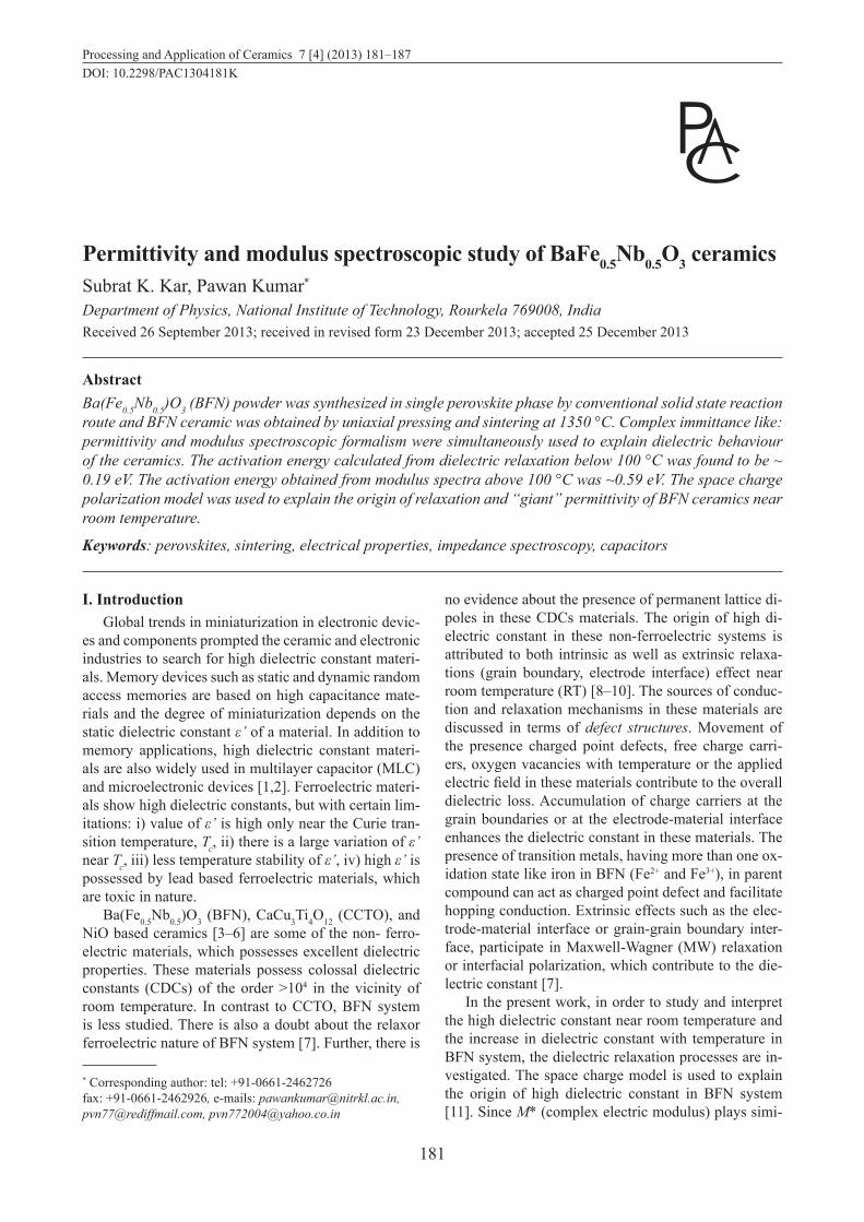
181
Processing and Application of Ceramics 7 [4] (2013) 181ndash187
Permittivity and modulus spectroscopic study of BaFe05Nb05O3 ceramicsSubrat K Kar Pawan Kumar
Department of Physics National Institute of Technology Rourkela 769008 IndiaReceived 26 September 2013 received in revised form 23 December 2013 accepted 25 December 2013
AbstractBa(Fe05Nb05)O3 (BFN) powder was synthesized in single perovskite phase by conventional solid state reaction route and BFN ceramic was obtained by uniaxial pressing and sintering at 1350 degC Complex immittance like permittivity and modulus spectroscopic formalism were simultaneously used to explain dielectric behaviour of the ceramics The activation energy calculated from dielectric relaxation below 100 degC was found to be ~ 019 eV The activation energy obtained from modulus spectra above 100 degC was ~059 eV The space charge polarization model was used to explain the origin of relaxation and ldquogiantrdquo permittivity of BFN ceramics near room temperature
Keywords perovskites sintering electrical properties impedance spectroscopy capacitors
I IntroductionGlobal trends in miniaturization in electronic devic-
es and components prompted the ceramic and electronic industries to search for high dielectric constant materi-als Memory devices such as static and dynamic random access memories are based on high capacitance mate-rials and the degree of miniaturization depends on the static dielectric constant εrsquo of a material In addition to memory applications high dielectric constant materi-als are also widely used in multilayer capacitor (MLC) and microelectronic devices [12] Ferroelectric materi-als show high dielectric constants but with certain lim-itations i) value of εrsquo is high only near the Curie tran-sition temperature Tc ii) there is a large variation of εrsquo near Tc iii) less temperature stability of εrsquo iv) high εrsquo is possessed by lead based ferroelectric materials which are toxic in nature
Ba(Fe05Nb05)O3 (BFN) CaCu3Ti4O12 (CCTO) and NiO based ceramics [3ndash6] are some of the non- ferro-electric materials which possesses excellent dielectric properties These materials possess colossal dielectric constants (CDCs) of the order gt104 in the vicinity of room temperature In contrast to CCTO BFN system is less studied There is also a doubt about the relaxor ferroelectric nature of BFN system [7] Further there is
no evidence about the presence of permanent lattice di-poles in these CDCs materials The origin of high di-electric constant in these non-ferroelectric systems is attributed to both intrinsic as well as extrinsic relaxa-tions (grain boundary electrode interface) effect near room temperature (RT) [8ndash10] The sources of conduc-tion and relaxation mechanisms in these materials are discussed in terms of defect structures Movement of the presence charged point defects free charge carri-ers oxygen vacancies with temperature or the applied electric field in these materials contribute to the overall dielectric loss Accumulation of charge carriers at the grain boundaries or at the electrode-material interface enhances the dielectric constant in these materials The presence of transition metals having more than one ox-idation state like iron in BFN (Fe2+ and Fe3+) in parent compound can act as charged point defect and facilitate hopping conduction Extrinsic effects such as the elec-trode-material interface or grain-grain boundary inter-face participate in Maxwell-Wagner (MW) relaxation or interfacial polarization which contribute to the die-lectric constant [7]
In the present work in order to study and interpret the high dielectric constant near room temperature and the increase in dielectric constant with temperature in BFN system the dielectric relaxation processes are in-vestigated The space charge model is used to explain the origin of high dielectric constant in BFN system [11] Since M (complex electric modulus) plays simi-
Corresponding author tel +91-0661-2462726fax +91-0661-2462926 e-mails pawankumarnitrklacin pvn77rediffmailcom pvn772004yahoocoin
DOI 102298PAC1304181K
182
SK Kar amp P Kumar Processing and Application of Ceramics 7 [4] (2013) 181ndash187
lar type of mechanism as that of ε (complex permittiv-ity) the simultaneous study of both these complex im-mittance parameters may be helpful in the explanation for the involved processes
II Experimental detailsBa(Fe05Nb05)O3 ceramic samples were prepared by
using solid state reaction route Stoichiometric propor-tions of BaCO3 Fe2O3 and Nb2O5 (all Merck India with gt99 purity) were used as the starting initial reagents The oxide powder was thoroughly mixed with acetone and ball milled for 12 h using zirconia balls Calcina-tions were carried out at 1250 degC for 4 h X-ray powder diffractometer (PHILIPS PW 3020) was used for cal-cined powder diffraction pattern analysis The calcined powder was grounded and mixed with 3 wt PVA (polyvinyl alcohol) as binder Then the ceramic powder was uniaxially pressed at 90 MPa in the form of discs of diameter ~10 mm and thickness ~1 mm These ceramic discs were sintered at 1350 degC for 4 h The microstruc-ture and surface morphology were analysed by using scanning electron microscope (JEOL SEM 6480LV) The sintered pellets were electroded using silver paste The dielectric properties measurements as a function of frequency (100 Hzndash1 MHz) and in the temperature range from the room temperature to 400 degC were carried out by using LCR meter (HIOKI 3532-50)
III Results and discussion
31 Structural and microstructural analysisThe X-ray diffraction (XRD) pattern of the calcined
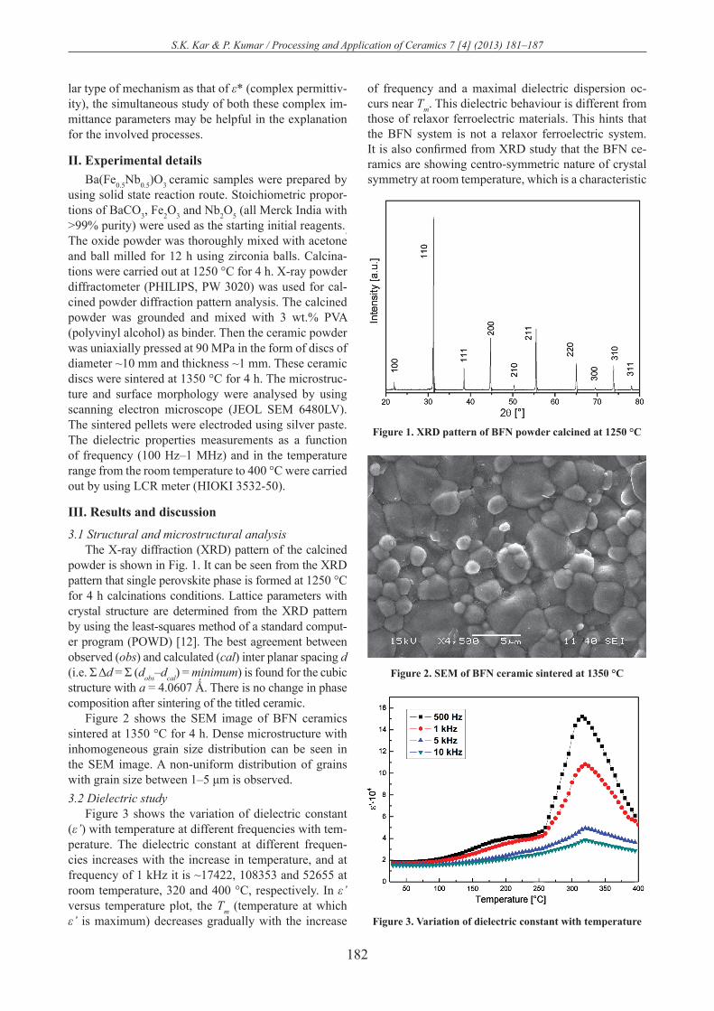
powder is shown in Fig 1 It can be seen from the XRD pattern that single perovskite phase is formed at 1250 degC for 4 h calcinations conditions Lattice parameters with crystal structure are determined from the XRD pattern by using the least-squares method of a standard comput-er program (POWD) [12] The best agreement between observed (obs) and calculated (cal) inter planar spacing d (ie Σ Δd = Σ (dobsndashdcal) = minimum) is found for the cubic structure with a = 40607 Ǻ There is no change in phase composition after sintering of the titled ceramic
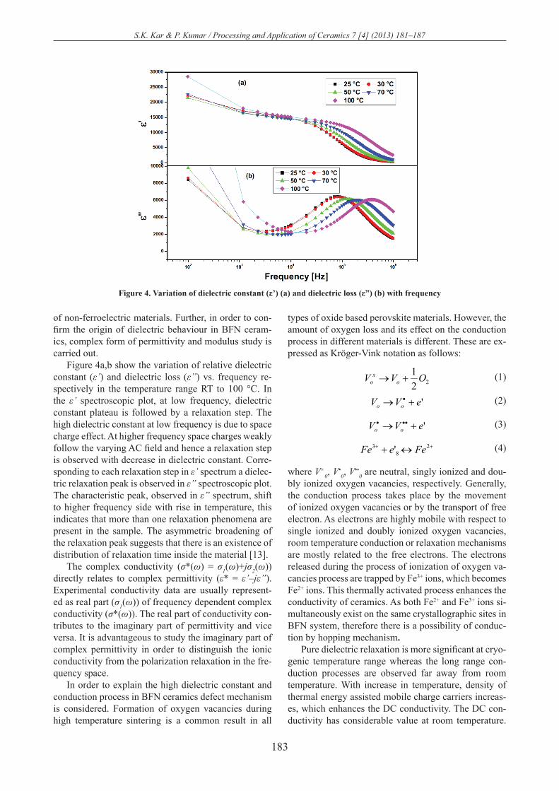
Figure 2 shows the SEM image of BFN ceramics sintered at 1350 degC for 4 h Dense microstructure with inhomogeneous grain size distribution can be seen in the SEM image A non-uniform distribution of grains with grain size between 1ndash5 μm is observed32 Dielectric study
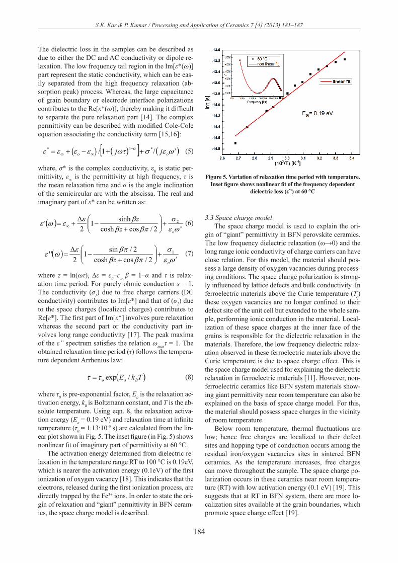
Figure 3 shows the variation of dielectric constant (εrsquo) with temperature at different frequencies with tem-perature The dielectric constant at different frequen-cies increases with the increase in temperature and at frequency of 1 kHz it is ~17422 108353 and 52655 at room temperature 320 and 400 degC respectively In εrsquo versus temperature plot the Tm (temperature at which εrsquo is maximum) decreases gradually with the increase
of frequency and a maximal dielectric dispersion oc-curs near Tm This dielectric behaviour is different from those of relaxor ferroelectric materials This hints that the BFN system is not a relaxor ferroelectric system It is also confirmed from XRD study that the BFN ce-ramics are showing centro-symmetric nature of crystal symmetry at room temperature which is a characteristic
Figure 3 Variation of dielectric constant with temperature
Figure 2 SEM of BFN ceramic sintered at 1350 degC
Figure 1 XRD pattern of BFN powder calcined at 1250 degC
183
SK Kar amp P Kumar Processing and Application of Ceramics 7 [4] (2013) 181ndash187
of non-ferroelectric materials Further in order to con-firm the origin of dielectric behaviour in BFN ceram-ics complex form of permittivity and modulus study is carried out
Figure 4ab show the variation of relative dielectric constant (εrsquo) and dielectric loss (εrdquo) vs frequency re-spectively in the temperature range RT to 100 degC In the εrsquo spectroscopic plot at low frequency dielectric constant plateau is followed by a relaxation step The high dielectric constant at low frequency is due to space charge effect At higher frequency space charges weakly follow the varying AC field and hence a relaxation step is observed with decrease in dielectric constant Corre-sponding to each relaxation step in εrsquo spectrum a dielec-tric relaxation peak is observed in εrdquo spectroscopic plot The characteristic peak observed in εrdquo spectrum shift to higher frequency side with rise in temperature this indicates that more than one relaxation phenomena are present in the sample The asymmetric broadening of the relaxation peak suggests that there is an existence of distribution of relaxation time inside the material [13]
The complex conductivity (σ(ω) = σ1(ω)+jσ2(ω)) directly relates to complex permittivity (ε = εrsquondashjεrdquo) Experimental conductivity data are usually represent-ed as real part (σ1(ω)) of frequency dependent complex conductivity (σ(ω)) The real part of conductivity con-tributes to the imaginary part of permittivity and vice versa It is advantageous to study the imaginary part of complex permittivity in order to distinguish the ionic conductivity from the polarization relaxation in the fre-quency space
In order to explain the high dielectric constant and conduction process in BFN ceramics defect mechanism is considered Formation of oxygen vacancies during high temperature sintering is a common result in all
types of oxide based perovskite materials However the amount of oxygen loss and its effect on the conduction process in different materials is different These are ex-pressed as Kroumlger-Vink notation as follows
(1)
(2)
(3)
(4)
where Vtimes0 V
bull0 V
bullbull0 are neutral singly ionized and dou-
bly ionized oxygen vacancies respectively Generally the conduction process takes place by the movement of ionized oxygen vacancies or by the transport of free electron As electrons are highly mobile with respect to single ionized and doubly ionized oxygen vacancies room temperature conduction or relaxation mechanisms are mostly related to the free electrons The electrons released during the process of ionization of oxygen va-cancies process are trapped by Fe3+ ions which becomes Fe2+ ions This thermally activated process enhances the conductivity of ceramics As both Fe2+ and Fe3+ ions si-multaneously exist on the same crystallographic sites in BFN system therefore there is a possibility of conduc-tion by hopping mechanism
Pure dielectric relaxation is more significant at cryo-genic temperature range whereas the long range con-duction processes are observed far away from room temperature With increase in temperature density of thermal energy assisted mobile charge carriers increas-es which enhances the DC conductivity The DC con-ductivity has considerable value at room temperature
Figure 4 Variation of dielectric constant (εrsquo) (a) and dielectric loss (εrdquo) (b) with frequency
22
1 OVV ox
o +rarr
eVV oo +rarr bull
eVV oo +rarr bullbullbull
++ harr+ 28
3 FeeFe
184
SK Kar amp P Kumar Processing and Application of Ceramics 7 [4] (2013) 181ndash187
The dielectric loss in the samples can be described as due to either the DC and AC conductivity or dipole re-laxation The low frequency tail region in the Im[ε(ω)] part represent the static conductivity which can be eas-ily separated from the high frequency relaxation (ab-sorption peak) process Whereas the large capacitance of grain boundary or electrode interface polarizations contributes to the Re[ε(ω)] thereby making it difficult to separate the pure relaxation part [14] The complex permittivity can be described with modified Cole-Cole equation associating the conductivity term [1516]
(5)
where σ is the complex conductivity ε0 is static per-mittivity εinfin is the permittivity at high frequency τ is the mean relaxation time and α is the angle inclination of the semicircular arc with the abscissa The real and imaginary part of ε can be written as
(6)
(7)
where z = ln(ωτ) ∆ε = ε0ndashεinfin β = 1ndashα and τ is relax-ation time period For purely ohmic conduction s = 1 The conductivity (σ1) due to free charge carriers (DC conductivity) contributes to Im[ε] and that of (σ2) due to the space charges (localized charges) contributes to Re[ε] The first part of Im[ε] involves pure relaxation whereas the second part or the conductivity part in-volves long range conductivity [17] The peak maxima of the εrdquo spectrum satisfies the relation ωmaxτ = 1 The obtained relaxation time period (τ) follows the tempera-ture dependent Arrhenius law
(8)
where τ0 is pre-exponential factor Ea is the relaxation ac-tivation energy kB is Boltzmann constant and T is the ab-solute temperature Using eqn 8 the relaxation activa-tion energy (Ea = 019 eV) and relaxation time at infinite temperature (τ0 = 11310-9 s) are calculated from the lin-ear plot shown in Fig 5 The inset figure (in Fig 5) shows nonlinear fit of imaginary part of permittivity at 60 degC
The activation energy determined from dielectric re-laxation in the temperature range RT to 100 degC is 019eV which is nearer the activation energy (01eV) of the first ionization of oxygen vacancy [18] This indicates that the electrons released during the first ionization process are directly trapped by the Fe3+ ions In order to state the ori-gin of relaxation and ldquogiantrdquo permittivity in BFN ceram-ics the space charge model is described
33 Space charge modelThe space charge model is used to explain the ori-
gin of ldquogiantrdquo permittivity in BFN perovskite ceramics The low frequency dielectric relaxation (ωrarr0) and the long range ionic conductivity of charge carriers can have close relation For this model the material should pos-sess a large density of oxygen vacancies during process-ing conditions The space charge polarization is strong-ly influenced by lattice defects and bulk conductivity In ferroelectric materials above the Curie temperature (Tc) these oxygen vacancies are no longer confined to their defect site of the unit cell but extended to the whole sam-ple performing ionic conduction in the material Local-ization of these space charges at the inner face of the grains is responsible for the dielectric relaxation in the materials Therefore the low frequency dielectric relax-ation observed in these ferroelectric materials above the Curie temperature is due to space charge effect This is the space charge model used for explaining the dielectric relaxation in ferroelectric materials [11] However non-ferroelectric ceramics like BFN system materials show-ing giant permittivity near room temperature can also be explained on the basis of space charge model For this the material should possess space charges in the vicinity of room temperature
Below room temperature thermal fluctuations are low hence free charges are localized to their defect sites and hopping type of conduction occurs among the residual ironoxygen vacancies sites in sintered BFN ceramics As the temperature increases free charges can move throughout the sample The space charge po-larization occurs in these ceramics near room tempera-ture (RT) with low activation energy (01 eV) [19] This suggests that at RT in BFN system there are more lo-calization sites available at the grain boundaries which promote space charge effect [19]
Figure 5 Variation of relaxation time period with temperature Inset figure shows nonlinear fit of the frequency dependent
dielectric loss (εrdquo) at 60 degC
(( ()) )[ ] soo jj ωεσωτεεεε α 1 1 ++minus+= minus
infininfin
( ) soz
zωεσ
βπββεεωε 2
2coscoshsinh1
2 +
+
minus∆
+= infin
)( soz ωεσ
βπββπεωε 1
2coscosh2sin1
2 +
+
minus∆
=
) ( TkE Bao expττ =
185
SK Kar amp P Kumar Processing and Application of Ceramics 7 [4] (2013) 181ndash187
The charged point defects (V0) formed at higher sin-tering temperature become fixed to the ionic site of the unit cell when the samples are cooled down to room temperature These ionized electrons take part in con-duction process near room temperature Accumula-tion of these charge carriers at the inner boundaries of grain increase the overall dielectric permittivity Here the grain boundary act as thin capacitor and the accu-mulated charges at the interfaces acts as electrodes for these capacitors which helps in increasing the dielec-tric permittivity of the BFN ceramics Also the low val-ue of activation energy (019 eV) fits well with the mi-croscopic Maxwell-Wagner relaxation [19] Hence the giant dielectric constant of BFN ceramics near room temperature of BFN ceramics is due to microscopic ef-fect of MW relaxation called as space charge polariza-tion The space charge model is fitted well with our re-sult near room temperature
34 Modulus studyThe electric modulus M is given by the inverse of
complex dielectric permittivity and can be expressed in the following form [20]
(9)
where Mrsquo = εrsquo(εrsquo2+εrdquo2) and Mrdquo = εrdquo(εrsquo2+εrdquo2) are real and imaginary part of complex modulus respectively The Mrsquo and Mrdquo vs frequency at different temperatures are plotted in Figs 6a and 6b respectively The relax-ation peak in Mrdquo spectrum is not observed in the low temperature region (lt 100 degC) whereas it starts appear-ing above 100 degC This may be due to the fact that the chosen range of frequency (100 Hz to 1 MHz) is lower than the range in which the Mrdquo relaxation peak falls or the range in which the relaxation ratio (r = ε0εinfin where ε0 and εinfin are dielectric constant at low and high frequen-cy respectively) increases [21] In the Mrdquo versus fre-quency spectrum two relaxation peaks can be expected corresponding to grain and grain boundary effects re-spectively One relaxation peak appears in low frequen-cy region due to the contribution from grain boundar-ies while the other appearing in high frequency region is due to the contribution from grains Both these relax-ation peaks in a sample will appear provided that the ca-pacitance of grains and grain boundaries are nearly the same [22] As Mrdquo = ε02C which means peaks corre-sponding to the large capacitance are diminished in the Mrdquo plot Therefore the relaxation peak corresponding to electrode interface which has larger capacitances is suppressed in the Mrdquo vs frequency plot As shown in Fig 6b the grain and grain boundary relaxations can be observed in the high and low frequency regions respec-tively The incomplete relaxation peak appears at higher frequency in Mrdquo spectroscopic plot which is due to the fact that the range of frequency chosen is not sufficient
Figure 6 Variation of real (a) and imaginary part (b) of electric modulus with frequency at different indicated measurement temperatures
a) b)
Figure 7 Variation of relaxation time period with temperature obtained from fitting the ima-ginary part of modulus Inset
figure shows non-linear fit of imaginary partof modulus at 250 degC
) ( )()()( ωωωεω 1 MMM +==
186
SK Kar amp P Kumar Processing and Application of Ceramics 7 [4] (2013) 181ndash187
for this process to be observed The characteristic peak maxima of Mrdquo spectroscopic plot obey the relation ωmax τ = 1 The low frequency data is fitted by using the fol-lowing formula [2324]
(10)
The obtained relaxation time τ (= 1ωmax) at differ-ent temperatures follows temperature dependent Arrhe-nius law (eqn 8) The activation energy obtained from linear fit (Fig 7) is ~059 eV and τ0=17times10-12 This val-ue is closer (07 eV) to that of second ionization from oxygen vacancy V0
bullbull [25] Therefore it can be conclud-ed that the oxygen vacancies mainly play important role in different types of relaxation processes and origin of giant dielectric constant in BFN systems The inset fig-ure (Fig 7) shows nonlinear fit of frequency dependent imaginary part of modulus at 250 degC35 Space Charge Model at High Temperature
At higher temperature (gt100 degC) electrons released from doubly ionized oxygen vacancy move towards the grain boundary In polycrystalline materials grain bound-aries play significant roles in their electrical properties A Schottky barrier can be formed at the grain boundar-ies The interfacial or Maxwell-Wagner polarization aris-es from Schottky barrier Large activation energy (059 eV) is required for such interfacial polarization
IV ConclusionsDielectric relaxation was studied in a wide temper-
ature range The relaxation activation energy was 019 eV and 059 eV in low and high temperature range cal-culated from permittivity and modulus formalism re-spectively Near room temperature (lt 100 degC) and above 100 degC free electrons released from first-ioniza-tion and second ionization of oxygen vacancies were seen to take part in the respective relaxation process-es The experimental data fitted well for explaining the space charge model for the origin of high dielectric con-stant near room temperature in BFN system
References1 N Setter R Waser ldquoElectroceramic materialsrdquo Acta
Mater 48 [1] (2000) 151ndash1782 SM Spearing ldquoMaterials issues in microelectro-
mechanical systems (MEMS)rdquo Acta Mater 48 [1] (2000) 179ndash196
3 S Saha TP Sinha ldquoLow-temperature scaling behav-ior of BaFe05Nb05O3rdquo Phys Rev B Condens Matter 65 [13] (2002) 134103
4 AP Ramirez MA Subramanian M Gardel G Blumberg D Li T Vogt SM Shapiro ldquoGiant die-lectric constant response in a copper-titanaterdquo Solid State Commun 115 [5] (2000) 217ndash220
5 MA Subramanian D Li N Duan BA Reisner AW Sleight ldquoHigh dielectric constant in ACu3Ti4O12 and ACu3Ti3FeO12 phasesrdquo J Solid State Chem 151 [2] (2000) 323ndash325
6 J Wu C-W Nan Y Lin Y Deng ldquoGiant dielectric permittivity observed in Li and Ti doped NiOrdquo Phys Rev Lett 89 [21] (2002) 217601
7 IP Raevski SA Prosandeev AS Bogatin MA Malitskaya L Jastrabik ldquoHigh dielectric permittiv-ity in AFe12B12O3 nonferroelectric perovskite ceram-ics (A = Ba Sr Ca B = Nb Ta Sb)rdquo J Appl Phys 93 [7] (2003) 4130ndash4136
8 DC Sinclair TB Adams FD Morrison AR West ldquoCaCu3Ti4O12 One-step internal barrier layer capaci-torrdquo Appl Phys Lett 80 [12] (2002) 2153ndash2155
9 G Deng P Muralt ldquoOn origin and intrinsic electrical properties of the colossal dielectric constant state in Ca-Cu3Ti4O12rdquo pp 012016 in IOP Conf Ser Mater Sci Eng Vol 8 IOP Publishing 2010
10 P Lunkenheimer R Fichtl SG Ebbinghaus A Loidl ldquoNonintrinsic origin of the colossal dielectric constants in CaCu3Ti4O12rdquo Phys Rev B Condens Matter 70 [17] (2004) 172102
11 O Bidault P Goux M Kchikech M Belkaoumi M Ma-glione ldquoSpace-charge relaxation in perovskitesrdquo Phys Rev B Condens Matter 49 [12] (1994) 7868ndash7873
12 E Wu ldquoPOWD an interactive program for powder diffraction data interpretation and indexingrdquo J Appl Crystallogr 22 [5] (1989) 506-510
13 DK Mahato A Dutta TP Sinha ldquoDielectric relax-ation in double perovskite oxide Ho2CdTiO6rdquo Bull Mater Sci 34 [3] (2011) 455ndash462
14 KL Ngai RW Rendell ldquoInterpreting the real part of the dielectric permittivity contributed by mobile ions in ionically conducting materialsrdquo Phys Rev B Con-dens Matter 61 [14] (2000) 9393ndash9398
15 KS Cole RH Cole ldquoDispersion and absorption in dielectrics I Alternating current characteristicsrdquo J Chem Phys 9 [4] (1941) 341ndash351
16 G Georgoussis A Kanapitsas P Pissis YV Savelyev VY Veselov EG Privalko ldquoStructure-property relation-ships in segmented polyurethanes with metal chelates in the main chainrdquo Eur Polym J 36 (2000) 1113ndash1126
17 T Prasit T Suwat Y Teerapon M Santi ldquoDielec-tric relaxation and dielectric response mechanism in (LiTi)-doped NiO ceramicsrdquo J Phys Condens Matter 20 [39] (2008) 395227
18 J Daniels KH Hardtl ldquoElectrical conductivity at high temperatures of donor-doped barium titanate ce-ramicsrdquo Philips Res Rep 31 (1976) 489ndash504
19 M Maglione ldquoPolarons free charge localisation and effective dielectric permittivity in oxidesrdquo pp 3719 in arXiv e-prints 10063719 2010
20 JR Macdonald ldquoImpedance spectroscopyrdquo Ann Bi-omed Eng 20 [3] (1992) 289ndash305
21 R Gerhardt ldquoImpedance and dielectric spectrosco-py revisited Distinguishing localized relaxation from long-range conductivityrdquo J Phys Chem Solids 55 [12] (1994) 1491ndash1506
))
((
+
+
+minus
=β
ωω
ωωβ
βββ
ω
max
max
max
11
MM
187
SK Kar amp P Kumar Processing and Application of Ceramics 7 [4] (2013) 181ndash187
22 DC Sinclair AR West ldquoImpedance and modulus spectroscopy of semiconducting BaTiO3 showing pos-itive temperature coefficient of resistancerdquo J Appl Phys 66 [8] (1989) 3850ndash3856
23 R Bergman ldquoGeneral susceptibility functions for re-laxations in disordered systemsrdquo J Appl Phys 88 [3] (2000) 1356ndash1365
24 CR Mariappan G Govindaraj SV Rathan GV Prakash ldquoVitrification of K3M2P3O12 (M = B Al Bi) NASICON-type materials and electrical relaxation studiesrdquo Mater Sci Eng B 123 [1] (2005) 63ndash68
25 SA Long RN Blumenthal ldquoTi-rich nonstoichi-ometric BaTiO3 II Analysis of defect structurerdquo J Am Ceram Soc 54 [11] (1971) 577ndash583
182
SK Kar amp P Kumar Processing and Application of Ceramics 7 [4] (2013) 181ndash187
lar type of mechanism as that of ε (complex permittiv-ity) the simultaneous study of both these complex im-mittance parameters may be helpful in the explanation for the involved processes
II Experimental detailsBa(Fe05Nb05)O3 ceramic samples were prepared by
using solid state reaction route Stoichiometric propor-tions of BaCO3 Fe2O3 and Nb2O5 (all Merck India with gt99 purity) were used as the starting initial reagents The oxide powder was thoroughly mixed with acetone and ball milled for 12 h using zirconia balls Calcina-tions were carried out at 1250 degC for 4 h X-ray powder diffractometer (PHILIPS PW 3020) was used for cal-cined powder diffraction pattern analysis The calcined powder was grounded and mixed with 3 wt PVA (polyvinyl alcohol) as binder Then the ceramic powder was uniaxially pressed at 90 MPa in the form of discs of diameter ~10 mm and thickness ~1 mm These ceramic discs were sintered at 1350 degC for 4 h The microstruc-ture and surface morphology were analysed by using scanning electron microscope (JEOL SEM 6480LV) The sintered pellets were electroded using silver paste The dielectric properties measurements as a function of frequency (100 Hzndash1 MHz) and in the temperature range from the room temperature to 400 degC were carried out by using LCR meter (HIOKI 3532-50)
III Results and discussion
31 Structural and microstructural analysisThe X-ray diffraction (XRD) pattern of the calcined
powder is shown in Fig 1 It can be seen from the XRD pattern that single perovskite phase is formed at 1250 degC for 4 h calcinations conditions Lattice parameters with crystal structure are determined from the XRD pattern by using the least-squares method of a standard comput-er program (POWD) [12] The best agreement between observed (obs) and calculated (cal) inter planar spacing d (ie Σ Δd = Σ (dobsndashdcal) = minimum) is found for the cubic structure with a = 40607 Ǻ There is no change in phase composition after sintering of the titled ceramic
Figure 2 shows the SEM image of BFN ceramics sintered at 1350 degC for 4 h Dense microstructure with inhomogeneous grain size distribution can be seen in the SEM image A non-uniform distribution of grains with grain size between 1ndash5 μm is observed32 Dielectric study
Figure 3 shows the variation of dielectric constant (εrsquo) with temperature at different frequencies with tem-perature The dielectric constant at different frequen-cies increases with the increase in temperature and at frequency of 1 kHz it is ~17422 108353 and 52655 at room temperature 320 and 400 degC respectively In εrsquo versus temperature plot the Tm (temperature at which εrsquo is maximum) decreases gradually with the increase
of frequency and a maximal dielectric dispersion oc-curs near Tm This dielectric behaviour is different from those of relaxor ferroelectric materials This hints that the BFN system is not a relaxor ferroelectric system It is also confirmed from XRD study that the BFN ce-ramics are showing centro-symmetric nature of crystal symmetry at room temperature which is a characteristic
Figure 3 Variation of dielectric constant with temperature
Figure 2 SEM of BFN ceramic sintered at 1350 degC
Figure 1 XRD pattern of BFN powder calcined at 1250 degC
183
SK Kar amp P Kumar Processing and Application of Ceramics 7 [4] (2013) 181ndash187
of non-ferroelectric materials Further in order to con-firm the origin of dielectric behaviour in BFN ceram-ics complex form of permittivity and modulus study is carried out
Figure 4ab show the variation of relative dielectric constant (εrsquo) and dielectric loss (εrdquo) vs frequency re-spectively in the temperature range RT to 100 degC In the εrsquo spectroscopic plot at low frequency dielectric constant plateau is followed by a relaxation step The high dielectric constant at low frequency is due to space charge effect At higher frequency space charges weakly follow the varying AC field and hence a relaxation step is observed with decrease in dielectric constant Corre-sponding to each relaxation step in εrsquo spectrum a dielec-tric relaxation peak is observed in εrdquo spectroscopic plot The characteristic peak observed in εrdquo spectrum shift to higher frequency side with rise in temperature this indicates that more than one relaxation phenomena are present in the sample The asymmetric broadening of the relaxation peak suggests that there is an existence of distribution of relaxation time inside the material [13]
The complex conductivity (σ(ω) = σ1(ω)+jσ2(ω)) directly relates to complex permittivity (ε = εrsquondashjεrdquo) Experimental conductivity data are usually represent-ed as real part (σ1(ω)) of frequency dependent complex conductivity (σ(ω)) The real part of conductivity con-tributes to the imaginary part of permittivity and vice versa It is advantageous to study the imaginary part of complex permittivity in order to distinguish the ionic conductivity from the polarization relaxation in the fre-quency space
In order to explain the high dielectric constant and conduction process in BFN ceramics defect mechanism is considered Formation of oxygen vacancies during high temperature sintering is a common result in all
types of oxide based perovskite materials However the amount of oxygen loss and its effect on the conduction process in different materials is different These are ex-pressed as Kroumlger-Vink notation as follows
(1)
(2)
(3)
(4)
where Vtimes0 V
bull0 V
bullbull0 are neutral singly ionized and dou-
bly ionized oxygen vacancies respectively Generally the conduction process takes place by the movement of ionized oxygen vacancies or by the transport of free electron As electrons are highly mobile with respect to single ionized and doubly ionized oxygen vacancies room temperature conduction or relaxation mechanisms are mostly related to the free electrons The electrons released during the process of ionization of oxygen va-cancies process are trapped by Fe3+ ions which becomes Fe2+ ions This thermally activated process enhances the conductivity of ceramics As both Fe2+ and Fe3+ ions si-multaneously exist on the same crystallographic sites in BFN system therefore there is a possibility of conduc-tion by hopping mechanism
Pure dielectric relaxation is more significant at cryo-genic temperature range whereas the long range con-duction processes are observed far away from room temperature With increase in temperature density of thermal energy assisted mobile charge carriers increas-es which enhances the DC conductivity The DC con-ductivity has considerable value at room temperature
Figure 4 Variation of dielectric constant (εrsquo) (a) and dielectric loss (εrdquo) (b) with frequency
22
1 OVV ox
o +rarr
eVV oo +rarr bull
eVV oo +rarr bullbullbull
++ harr+ 28
3 FeeFe
184
SK Kar amp P Kumar Processing and Application of Ceramics 7 [4] (2013) 181ndash187
The dielectric loss in the samples can be described as due to either the DC and AC conductivity or dipole re-laxation The low frequency tail region in the Im[ε(ω)] part represent the static conductivity which can be eas-ily separated from the high frequency relaxation (ab-sorption peak) process Whereas the large capacitance of grain boundary or electrode interface polarizations contributes to the Re[ε(ω)] thereby making it difficult to separate the pure relaxation part [14] The complex permittivity can be described with modified Cole-Cole equation associating the conductivity term [1516]
(5)
where σ is the complex conductivity ε0 is static per-mittivity εinfin is the permittivity at high frequency τ is the mean relaxation time and α is the angle inclination of the semicircular arc with the abscissa The real and imaginary part of ε can be written as
(6)
(7)
where z = ln(ωτ) ∆ε = ε0ndashεinfin β = 1ndashα and τ is relax-ation time period For purely ohmic conduction s = 1 The conductivity (σ1) due to free charge carriers (DC conductivity) contributes to Im[ε] and that of (σ2) due to the space charges (localized charges) contributes to Re[ε] The first part of Im[ε] involves pure relaxation whereas the second part or the conductivity part in-volves long range conductivity [17] The peak maxima of the εrdquo spectrum satisfies the relation ωmaxτ = 1 The obtained relaxation time period (τ) follows the tempera-ture dependent Arrhenius law
(8)
where τ0 is pre-exponential factor Ea is the relaxation ac-tivation energy kB is Boltzmann constant and T is the ab-solute temperature Using eqn 8 the relaxation activa-tion energy (Ea = 019 eV) and relaxation time at infinite temperature (τ0 = 11310-9 s) are calculated from the lin-ear plot shown in Fig 5 The inset figure (in Fig 5) shows nonlinear fit of imaginary part of permittivity at 60 degC
The activation energy determined from dielectric re-laxation in the temperature range RT to 100 degC is 019eV which is nearer the activation energy (01eV) of the first ionization of oxygen vacancy [18] This indicates that the electrons released during the first ionization process are directly trapped by the Fe3+ ions In order to state the ori-gin of relaxation and ldquogiantrdquo permittivity in BFN ceram-ics the space charge model is described
33 Space charge modelThe space charge model is used to explain the ori-
gin of ldquogiantrdquo permittivity in BFN perovskite ceramics The low frequency dielectric relaxation (ωrarr0) and the long range ionic conductivity of charge carriers can have close relation For this model the material should pos-sess a large density of oxygen vacancies during process-ing conditions The space charge polarization is strong-ly influenced by lattice defects and bulk conductivity In ferroelectric materials above the Curie temperature (Tc) these oxygen vacancies are no longer confined to their defect site of the unit cell but extended to the whole sam-ple performing ionic conduction in the material Local-ization of these space charges at the inner face of the grains is responsible for the dielectric relaxation in the materials Therefore the low frequency dielectric relax-ation observed in these ferroelectric materials above the Curie temperature is due to space charge effect This is the space charge model used for explaining the dielectric relaxation in ferroelectric materials [11] However non-ferroelectric ceramics like BFN system materials show-ing giant permittivity near room temperature can also be explained on the basis of space charge model For this the material should possess space charges in the vicinity of room temperature
Below room temperature thermal fluctuations are low hence free charges are localized to their defect sites and hopping type of conduction occurs among the residual ironoxygen vacancies sites in sintered BFN ceramics As the temperature increases free charges can move throughout the sample The space charge po-larization occurs in these ceramics near room tempera-ture (RT) with low activation energy (01 eV) [19] This suggests that at RT in BFN system there are more lo-calization sites available at the grain boundaries which promote space charge effect [19]
Figure 5 Variation of relaxation time period with temperature Inset figure shows nonlinear fit of the frequency dependent
dielectric loss (εrdquo) at 60 degC
(( ()) )[ ] soo jj ωεσωτεεεε α 1 1 ++minus+= minus
infininfin
( ) soz
zωεσ
βπββεεωε 2
2coscoshsinh1
2 +
+
minus∆
+= infin
)( soz ωεσ
βπββπεωε 1
2coscosh2sin1
2 +
+
minus∆
=
) ( TkE Bao expττ =
185
SK Kar amp P Kumar Processing and Application of Ceramics 7 [4] (2013) 181ndash187
The charged point defects (V0) formed at higher sin-tering temperature become fixed to the ionic site of the unit cell when the samples are cooled down to room temperature These ionized electrons take part in con-duction process near room temperature Accumula-tion of these charge carriers at the inner boundaries of grain increase the overall dielectric permittivity Here the grain boundary act as thin capacitor and the accu-mulated charges at the interfaces acts as electrodes for these capacitors which helps in increasing the dielec-tric permittivity of the BFN ceramics Also the low val-ue of activation energy (019 eV) fits well with the mi-croscopic Maxwell-Wagner relaxation [19] Hence the giant dielectric constant of BFN ceramics near room temperature of BFN ceramics is due to microscopic ef-fect of MW relaxation called as space charge polariza-tion The space charge model is fitted well with our re-sult near room temperature
34 Modulus studyThe electric modulus M is given by the inverse of
complex dielectric permittivity and can be expressed in the following form [20]
(9)
where Mrsquo = εrsquo(εrsquo2+εrdquo2) and Mrdquo = εrdquo(εrsquo2+εrdquo2) are real and imaginary part of complex modulus respectively The Mrsquo and Mrdquo vs frequency at different temperatures are plotted in Figs 6a and 6b respectively The relax-ation peak in Mrdquo spectrum is not observed in the low temperature region (lt 100 degC) whereas it starts appear-ing above 100 degC This may be due to the fact that the chosen range of frequency (100 Hz to 1 MHz) is lower than the range in which the Mrdquo relaxation peak falls or the range in which the relaxation ratio (r = ε0εinfin where ε0 and εinfin are dielectric constant at low and high frequen-cy respectively) increases [21] In the Mrdquo versus fre-quency spectrum two relaxation peaks can be expected corresponding to grain and grain boundary effects re-spectively One relaxation peak appears in low frequen-cy region due to the contribution from grain boundar-ies while the other appearing in high frequency region is due to the contribution from grains Both these relax-ation peaks in a sample will appear provided that the ca-pacitance of grains and grain boundaries are nearly the same [22] As Mrdquo = ε02C which means peaks corre-sponding to the large capacitance are diminished in the Mrdquo plot Therefore the relaxation peak corresponding to electrode interface which has larger capacitances is suppressed in the Mrdquo vs frequency plot As shown in Fig 6b the grain and grain boundary relaxations can be observed in the high and low frequency regions respec-tively The incomplete relaxation peak appears at higher frequency in Mrdquo spectroscopic plot which is due to the fact that the range of frequency chosen is not sufficient
Figure 6 Variation of real (a) and imaginary part (b) of electric modulus with frequency at different indicated measurement temperatures
a) b)
Figure 7 Variation of relaxation time period with temperature obtained from fitting the ima-ginary part of modulus Inset
figure shows non-linear fit of imaginary partof modulus at 250 degC
) ( )()()( ωωωεω 1 MMM +==
186
SK Kar amp P Kumar Processing and Application of Ceramics 7 [4] (2013) 181ndash187
for this process to be observed The characteristic peak maxima of Mrdquo spectroscopic plot obey the relation ωmax τ = 1 The low frequency data is fitted by using the fol-lowing formula [2324]
(10)
The obtained relaxation time τ (= 1ωmax) at differ-ent temperatures follows temperature dependent Arrhe-nius law (eqn 8) The activation energy obtained from linear fit (Fig 7) is ~059 eV and τ0=17times10-12 This val-ue is closer (07 eV) to that of second ionization from oxygen vacancy V0
bullbull [25] Therefore it can be conclud-ed that the oxygen vacancies mainly play important role in different types of relaxation processes and origin of giant dielectric constant in BFN systems The inset fig-ure (Fig 7) shows nonlinear fit of frequency dependent imaginary part of modulus at 250 degC35 Space Charge Model at High Temperature
At higher temperature (gt100 degC) electrons released from doubly ionized oxygen vacancy move towards the grain boundary In polycrystalline materials grain bound-aries play significant roles in their electrical properties A Schottky barrier can be formed at the grain boundar-ies The interfacial or Maxwell-Wagner polarization aris-es from Schottky barrier Large activation energy (059 eV) is required for such interfacial polarization
IV ConclusionsDielectric relaxation was studied in a wide temper-
ature range The relaxation activation energy was 019 eV and 059 eV in low and high temperature range cal-culated from permittivity and modulus formalism re-spectively Near room temperature (lt 100 degC) and above 100 degC free electrons released from first-ioniza-tion and second ionization of oxygen vacancies were seen to take part in the respective relaxation process-es The experimental data fitted well for explaining the space charge model for the origin of high dielectric con-stant near room temperature in BFN system
References1 N Setter R Waser ldquoElectroceramic materialsrdquo Acta
Mater 48 [1] (2000) 151ndash1782 SM Spearing ldquoMaterials issues in microelectro-
mechanical systems (MEMS)rdquo Acta Mater 48 [1] (2000) 179ndash196
3 S Saha TP Sinha ldquoLow-temperature scaling behav-ior of BaFe05Nb05O3rdquo Phys Rev B Condens Matter 65 [13] (2002) 134103
4 AP Ramirez MA Subramanian M Gardel G Blumberg D Li T Vogt SM Shapiro ldquoGiant die-lectric constant response in a copper-titanaterdquo Solid State Commun 115 [5] (2000) 217ndash220
5 MA Subramanian D Li N Duan BA Reisner AW Sleight ldquoHigh dielectric constant in ACu3Ti4O12 and ACu3Ti3FeO12 phasesrdquo J Solid State Chem 151 [2] (2000) 323ndash325
6 J Wu C-W Nan Y Lin Y Deng ldquoGiant dielectric permittivity observed in Li and Ti doped NiOrdquo Phys Rev Lett 89 [21] (2002) 217601
7 IP Raevski SA Prosandeev AS Bogatin MA Malitskaya L Jastrabik ldquoHigh dielectric permittiv-ity in AFe12B12O3 nonferroelectric perovskite ceram-ics (A = Ba Sr Ca B = Nb Ta Sb)rdquo J Appl Phys 93 [7] (2003) 4130ndash4136
8 DC Sinclair TB Adams FD Morrison AR West ldquoCaCu3Ti4O12 One-step internal barrier layer capaci-torrdquo Appl Phys Lett 80 [12] (2002) 2153ndash2155
9 G Deng P Muralt ldquoOn origin and intrinsic electrical properties of the colossal dielectric constant state in Ca-Cu3Ti4O12rdquo pp 012016 in IOP Conf Ser Mater Sci Eng Vol 8 IOP Publishing 2010
10 P Lunkenheimer R Fichtl SG Ebbinghaus A Loidl ldquoNonintrinsic origin of the colossal dielectric constants in CaCu3Ti4O12rdquo Phys Rev B Condens Matter 70 [17] (2004) 172102
11 O Bidault P Goux M Kchikech M Belkaoumi M Ma-glione ldquoSpace-charge relaxation in perovskitesrdquo Phys Rev B Condens Matter 49 [12] (1994) 7868ndash7873
12 E Wu ldquoPOWD an interactive program for powder diffraction data interpretation and indexingrdquo J Appl Crystallogr 22 [5] (1989) 506-510
13 DK Mahato A Dutta TP Sinha ldquoDielectric relax-ation in double perovskite oxide Ho2CdTiO6rdquo Bull Mater Sci 34 [3] (2011) 455ndash462
14 KL Ngai RW Rendell ldquoInterpreting the real part of the dielectric permittivity contributed by mobile ions in ionically conducting materialsrdquo Phys Rev B Con-dens Matter 61 [14] (2000) 9393ndash9398
15 KS Cole RH Cole ldquoDispersion and absorption in dielectrics I Alternating current characteristicsrdquo J Chem Phys 9 [4] (1941) 341ndash351
16 G Georgoussis A Kanapitsas P Pissis YV Savelyev VY Veselov EG Privalko ldquoStructure-property relation-ships in segmented polyurethanes with metal chelates in the main chainrdquo Eur Polym J 36 (2000) 1113ndash1126
17 T Prasit T Suwat Y Teerapon M Santi ldquoDielec-tric relaxation and dielectric response mechanism in (LiTi)-doped NiO ceramicsrdquo J Phys Condens Matter 20 [39] (2008) 395227
18 J Daniels KH Hardtl ldquoElectrical conductivity at high temperatures of donor-doped barium titanate ce-ramicsrdquo Philips Res Rep 31 (1976) 489ndash504
19 M Maglione ldquoPolarons free charge localisation and effective dielectric permittivity in oxidesrdquo pp 3719 in arXiv e-prints 10063719 2010
20 JR Macdonald ldquoImpedance spectroscopyrdquo Ann Bi-omed Eng 20 [3] (1992) 289ndash305
21 R Gerhardt ldquoImpedance and dielectric spectrosco-py revisited Distinguishing localized relaxation from long-range conductivityrdquo J Phys Chem Solids 55 [12] (1994) 1491ndash1506
))
((
+
+
+minus
=β
ωω
ωωβ
βββ
ω
max
max
max
11
MM
187
SK Kar amp P Kumar Processing and Application of Ceramics 7 [4] (2013) 181ndash187
22 DC Sinclair AR West ldquoImpedance and modulus spectroscopy of semiconducting BaTiO3 showing pos-itive temperature coefficient of resistancerdquo J Appl Phys 66 [8] (1989) 3850ndash3856
23 R Bergman ldquoGeneral susceptibility functions for re-laxations in disordered systemsrdquo J Appl Phys 88 [3] (2000) 1356ndash1365
24 CR Mariappan G Govindaraj SV Rathan GV Prakash ldquoVitrification of K3M2P3O12 (M = B Al Bi) NASICON-type materials and electrical relaxation studiesrdquo Mater Sci Eng B 123 [1] (2005) 63ndash68
25 SA Long RN Blumenthal ldquoTi-rich nonstoichi-ometric BaTiO3 II Analysis of defect structurerdquo J Am Ceram Soc 54 [11] (1971) 577ndash583
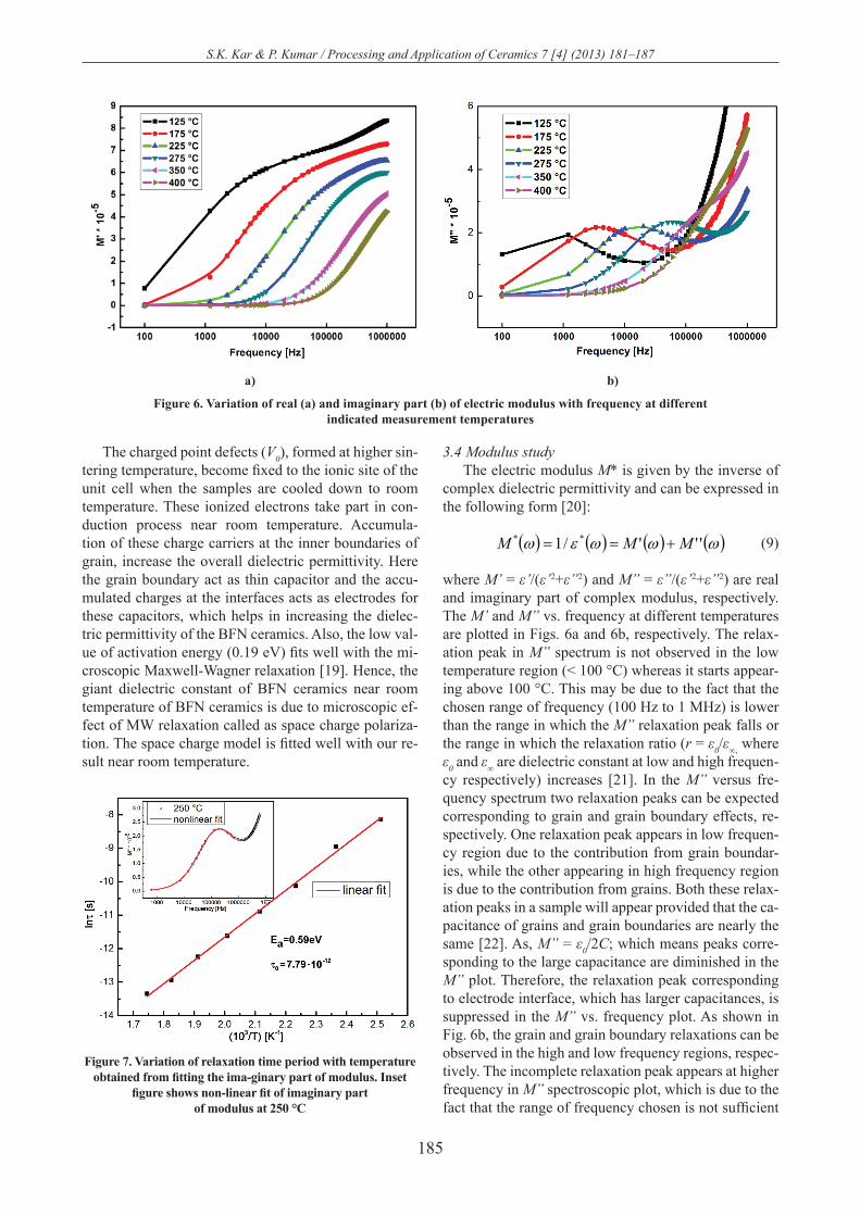