Embed Size (px)
Citation preview

3rd Year DSD CourseworkSingle-Component Sequential Baseline JPEG Decoderon an FPGA
Laurence Hey

The Task
• Design a hardware sequential baseline JPEG decoder– Working in pairs
• Implement design for the Xilinx Vertex II Pro FPGA– Test and demonstrate the design using the Xilinx
XUP Virtex II Pro Development System.
• Write a report detailing your design

Outline
• What this lecture will provide– Some background– JPEG theory– An example– Hints to get you started– Information on the hardware and tools
• What this lecture won’t provide– A step by step guide for you to follow
Background
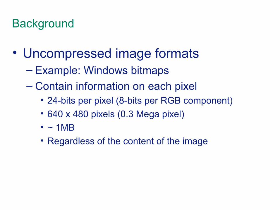
• Uncompressed image formats– Example: Windows bitmaps– Contain information on each pixel
• 24-bits per pixel (8-bits per RGB component)• 640 x 480 pixels (0.3 Mega pixel)• ~ 1MB• Regardless of the content of the image

Compression
• Lossless– No information lost → fully reversible– Theoretical limit → Shannon's entropy– Examples
• WinZip → General purpose• FLAC → audio• PNG → images
• Lossy– Information lost → not fully reversible– No theoretical limit– Examples
• MP3 → audio• JPEG → images
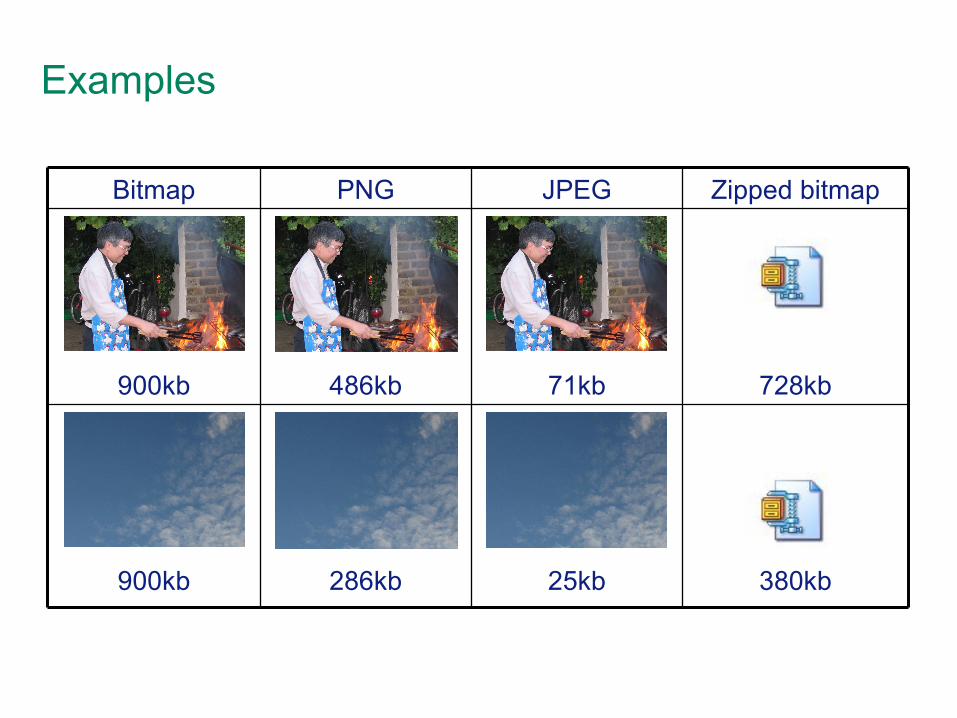
Examples
286kb
486kb
PNG
380kb25kb900kb
728kb71kb900kb
Zipped bitmapJPEGBitmap
JPEG theory
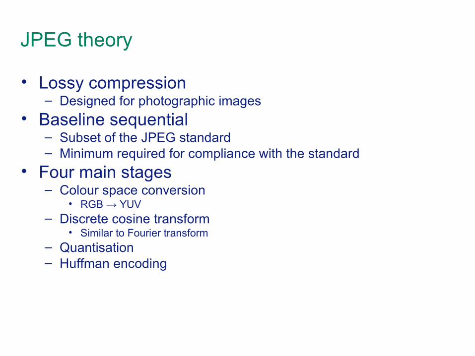
• Lossy compression– Designed for photographic images
• Baseline sequential– Subset of the JPEG standard– Minimum required for compliance with the standard
• Four main stages– Colour space conversion
• RGB → YUV – Discrete cosine transform
• Similar to Fourier transform– Quantisation– Huffman encoding

Coursework Simplifications
• Sequential Baseline• Single component (greyscale) only• Decoder must only work on a specific file
– File is provided– 640 x 480 pixels– Quantisation and Huffman tables can be hard
wired
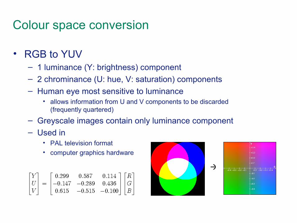
Colour space conversion
• RGB to YUV– 1 luminance (Y: brightness) component– 2 chrominance (U: hue, V: saturation) components– Human eye most sensitive to luminance
• allows information from U and V components to be discarded (frequently quartered)
– Greyscale images contain only luminance component– Used in
• PAL television format• computer graphics hardware

Image Blocks
• Each component of image is divided into blocks– 8 x 8 pixels in size– Arranged in raster scan (or similar)

Forward discrete cosine transform
where
( ) ( )16
12cos16
12cos41 7
0
7
0
ππ vyuxsCCSx y
xyvuvu++= ∑∑
= =
2/1, =vu CC 0, =vu
1, =vu CC
for
otherwise
Each block is converted into frequency space using the FDCT
vuS
value of source block pixel (x, y)xys
value of destination block pixel (v, u)

Example - FDCT
Original 8x8 block
128 is subtracted from each value
FDCT
DC component (larger than rest)
Values become smaller towards bottom right of block2’s complement notation
(taken from the wikipedia)

Example - Quantisation
Quantisation matrix (not the same as in the coursework)
The DCT coefficient block is divided by a quantisation matrix. This results in a block where many of the values go to zero.
This is the main lossy stage.

Huffman coding
The elements of the quantised DCT coefficient block are ordered in zigzag pattern as shown.
−26, −3, 0, −3, −3, −6, 2, −4, 1 −4, 1, 1, 5, 1, 2, −1, 1, −1, 2, 0, 0, 0, 0, 0, −1, −1, 0, 0, 0, 0, 0, 0, 0, 0, 0, 0, 0, 0, 0, 0, 0, 0, 0, 0, 0, 0, 0, 0, 0, 0, 0, 0, 0, 0, 0, 0, 0, 0, 0, 0, 0, 0, 0, 0
−26, −3, 0, −3, −3, −6, 2, −4, 1 −4, 1, 1, 5, 1, 2, −1, 1, −1, 2, 0, 0, 0, 0, 0, −1, −1, EOB
Huffman coding 2
• In order to further reduce the size of the DC component the quantised DC component of the previous block is subtracted from the current one
• If the code 0xFF ever appears a zero is “stuffed” in after it. These must be removed by the decoder
• See Annex F of the JPEG standard for more detailed information

Decoding
• The Reverse– Huffman decoding– Dequantisation– Inverse discrete cosine transform

Huffman decoding
• Hints on implementation– Use table look up – AC and DC Huffman tables are provided in file
tables.xls• These are entered as found in the JPEG file’s header• Described in Annex B of JPEG standard
– Decoding algorithm can be found in Annex F of the JPEG standard (specifically page 102+)

Dequantisation
The DCT coefficient block is multiplied by the quantisation matrix.
The zero values remain at zero.
This is a loss of information.

Inverse DCT
where
2/1, =vu CC 0, =vu
1, =vu CC
for
otherwise
Each block is converted back from frequency space using the IDCT
( ) ( )16
12cos16
12cos41 7
0
7
0
ππ vyuxSCCsu v
vuvuxy++= ∑∑
= =
vuSvalue of destination block pixel (x, y)xys
value of source block pixel (v, u)

Inverse DCT 2
• Hints on implementation– Buffer a block at a time– Pre-compute the cosine values (for table look-up)?– Use dedicated multipliers– Parallel! Parallel! Parallel!
• For each pixel you must multiply and sum 64 times

Example – Inverse DCT
Inverse DCT
Add 128

Example - Quality loss
Original Decoded
Difference:

Xilinx XUP Virtex II Pro Development System
(5 available)

Hardware – The FPGA
• Virtex II Pro XC2VP30• Highlights
– Big (30k+ logic elements)– 2 PowerPCs– 136 Multiplier blocks– 136 18kbit dual port block RAMs

The Design
• Software / Hardware co-design• Uses
– Flash memory card (reader) → storing JPEG– SDRAM– display– PowerPC → master– FPGA logic → slave
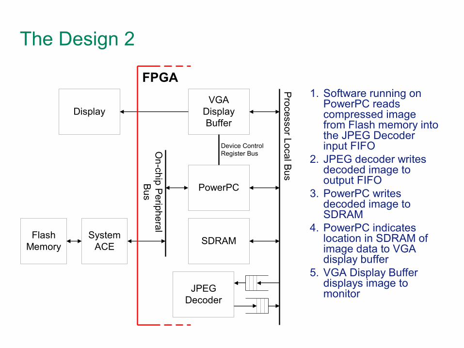
The Design 2
1. Software running on PowerPC reads compressed image from Flash memory into the JPEG Decoder input FIFO
2. JPEG decoder writes decoded image to output FIFO
3. PowerPC writes decoded image to SDRAM
4. PowerPC indicates location in SDRAM of image data to VGA display buffer
5. VGA Display Buffer displays image to monitor
PowerPC
VGADisplayBuffer
SDRAM
JPEGDecoder
SystemACE
FlashMemory
Processor Local B
us
On-chip P
eripheralB
us
Device ControlRegister Bus
Display
FPGA

The Design 3
• The IDCT block controls the input of data by setting data_req high. This filters through to the Huffman block
• data_in_en of Huffman block goes high when data is available from input FIFO
• Dequantisation block must set data_out_en high during the clock cycle before data is available on the output
Huffman
clk
rst
data_in
data_in_en
data_req
data_out
data_out_en
Dequantisation
clk
rst
data_in
data_in_en
data_out
data_out_en
IDCT
clk
rst
data_in
data_in_en
data_out
data_out_en
data_req data_reqdata_req_indata_req_in

The Tools
• Xilinx ISE (Project navigator)– Creating your design– Schematic template files provided
• Need to be converted to VHDL via the symbol generator
• Modelsim– Simulating and testing your design
• Xilinx EDK (Platform Studio)– Piecing together IP cores and software code– Generating bit-file and programming board
• All available in Mahanakorn lab on level 9

Deliverables
• Work in pairs– Divide task in two (e.g. Huffman & dequantisation; IDCT)
• Demonstrate design working on the board• Joint report
– Details of your design– Simulation results– How could it be expanded into a 3 component design?
• Deadline: 10th January 2006

Contact
• Meeting time– Two one hour sessions per week– Monday 1112– Friday 12– Suggestions?
• Email– [email protected]
• Website– http://cas.ee.ic.ac.uk/people/lah100/