Embed Size (px)
Citation preview

Virtex-4 Libraries Guide forSchematic Designs
ISE 10.1

Xilinx Trademarks and Copyright Information
Xilinx is disclosing this user guide, manual, release note, and/or specification (the “Documentation”) to yousolely for use in the development of designs to operate with Xilinx hardware devices. You may not reproduce,distribute, republish, download, display, post, or transmit the Documentation in any form or by any meansincluding, but not limited to, electronic, mechanical, photocopying, recording, or otherwise, without the priorwritten consent of Xilinx. Xilinx expressly disclaims any liability arising out of your use of the Documentation.Xilinx reserves the right, at its sole discretion, to change the Documentation without notice at any time. Xilinxassumes no obligation to correct any errors contained in the Documentation, or to advise you of any correctionsor updates. Xilinx expressly disclaims any liability in connection with technical support or assistance that may beprovided to you in connection with the Information.
THE DOCUMENTATION IS DISCLOSED TO YOU “AS-IS” WITH NOWARRANTY OF ANY KIND. XILINXMAKES NO OTHER WARRANTIES, WHETHER EXPRESS, IMPLIED, OR STATUTORY, REGARDINGTHE DOCUMENTATION, INCLUDING ANY WARRANTIES OF MERCHANTABILITY, FITNESS FOR APARTICULAR PURPOSE, OR NONINFRINGEMENT OF THIRD-PARTY RIGHTS. IN NO EVENT WILLXILINX BE LIABLE FOR ANY CONSEQUENTIAL, INDIRECT, EXEMPLARY, SPECIAL, OR INCIDENTALDAMAGES, INCLUDING ANY LOSS OF DATA OR LOST PROFITS, ARISING FROM YOUR USE OF THEDOCUMENTATION.
© Copyright 2002 – 2008 Xilinx, Inc. All Rights Reserved. XILINX, the Xilinx logo, the Brand Window and otherdesignated brands included herein are trademarks of Xilinx, Inc. All other trademarks are the property of theirrespective owners. The PowerPC name and logo are registered trademarks of IBM Corp., and used under license.All other trademarks are the property of their respective owners.
Libraries Guide
2 www.xilinx.com 10.1
Table of ContentsAbout this Guide ........................................................................................................................................ 13Functional Categories ................................................................................................................................. 15About Design Elements............................................................................................................................... 33
ACC16 ................................................................................................................................................ 34ACC4.................................................................................................................................................. 36ACC8.................................................................................................................................................. 38ADD16................................................................................................................................................ 40ADD4 ................................................................................................................................................. 42ADD8 ................................................................................................................................................. 44ADSU16 .............................................................................................................................................. 46ADSU4................................................................................................................................................ 48ADSU8................................................................................................................................................ 50AND12................................................................................................................................................ 52AND16................................................................................................................................................ 53AND2 ................................................................................................................................................. 54AND2B1.............................................................................................................................................. 55AND2B2.............................................................................................................................................. 56AND3 ................................................................................................................................................. 57AND3B1.............................................................................................................................................. 58AND3B2.............................................................................................................................................. 59AND3B3.............................................................................................................................................. 60AND4 ................................................................................................................................................. 61AND4B1.............................................................................................................................................. 62AND4B2.............................................................................................................................................. 63AND4B3.............................................................................................................................................. 64AND4B4.............................................................................................................................................. 65AND5 ................................................................................................................................................. 66AND5B1.............................................................................................................................................. 67AND5B2.............................................................................................................................................. 68AND5B3.............................................................................................................................................. 69AND5B4.............................................................................................................................................. 70AND5B5.............................................................................................................................................. 71AND6 ................................................................................................................................................. 72AND7 ................................................................................................................................................. 73AND8 ................................................................................................................................................. 74AND9 ................................................................................................................................................. 75BRLSHFT4 .......................................................................................................................................... 76BRLSHFT8 .......................................................................................................................................... 77BSCAN_VIRTEX4 ................................................................................................................................ 79BUF .................................................................................................................................................... 81BUFCF ................................................................................................................................................ 82BUFG.................................................................................................................................................. 83BUFGCE ............................................................................................................................................. 84BUFGCE_1 .......................................................................................................................................... 85BUFGCTRL ......................................................................................................................................... 86BUFGMUX.......................................................................................................................................... 88BUFGMUX_1....................................................................................................................................... 89BUFGMUX_VIRTEX4 .......................................................................................................................... 90BUFIO................................................................................................................................................. 91BUFR .................................................................................................................................................. 92CAPTURE_VIRTEX4............................................................................................................................ 94CB16CE............................................................................................................................................... 95CB16CLE............................................................................................................................................. 97CB16CLED .......................................................................................................................................... 99CB16RE.............................................................................................................................................. 101CB2CE ............................................................................................................................................... 103
Libraries Guide
10.1 www.xilinx.com 3
CB2CLE ............................................................................................................................................. 105CB2CLED........................................................................................................................................... 107CB2RE................................................................................................................................................ 109CB4CE ............................................................................................................................................... 111CB4CLE ............................................................................................................................................. 113CB4CLED........................................................................................................................................... 115CB4RE................................................................................................................................................ 117CB8CE ............................................................................................................................................... 119CB8CLE ............................................................................................................................................. 121CB8CLED........................................................................................................................................... 123CB8RE................................................................................................................................................ 125CC16CE ............................................................................................................................................. 127CC16CLE ........................................................................................................................................... 129CC16CLED......................................................................................................................................... 131CC16RE.............................................................................................................................................. 133CC8CE ............................................................................................................................................... 135CC8CLE ............................................................................................................................................. 137CC8CLED .......................................................................................................................................... 139CC8RE ............................................................................................................................................... 141CD4CE............................................................................................................................................... 143CD4CLE............................................................................................................................................. 145CD4RE ............................................................................................................................................... 147CD4RLE............................................................................................................................................. 149CJ4CE ................................................................................................................................................ 151CJ4RE ................................................................................................................................................ 152CJ5CE ................................................................................................................................................ 153CJ5RE ................................................................................................................................................ 154CJ8CE ................................................................................................................................................ 155CJ8RE ................................................................................................................................................ 156COMP16 ............................................................................................................................................ 157COMP2 .............................................................................................................................................. 158COMP4 .............................................................................................................................................. 159COMP8 .............................................................................................................................................. 160COMPM16 ......................................................................................................................................... 161COMPM2........................................................................................................................................... 163COMPM4........................................................................................................................................... 164COMPM8........................................................................................................................................... 165COMPMC16....................................................................................................................................... 167COMPMC8 ........................................................................................................................................ 169CR16CE.............................................................................................................................................. 171CR8CE ............................................................................................................................................... 172D2_4E ................................................................................................................................................ 173D3_8E ................................................................................................................................................ 174D4_16E............................................................................................................................................... 175DCIRESET.......................................................................................................................................... 176DCM_ADV ........................................................................................................................................ 177DCM_BASE........................................................................................................................................ 182DCM_PS ............................................................................................................................................ 186DEC_CC16 ......................................................................................................................................... 190DEC_CC4........................................................................................................................................... 192DEC_CC8........................................................................................................................................... 193DECODE16 ........................................................................................................................................ 194DECODE32 ........................................................................................................................................ 195DECODE4 .......................................................................................................................................... 196DECODE64 ........................................................................................................................................ 197DECODE8 .......................................................................................................................................... 198DSP48 ................................................................................................................................................ 199EMAC................................................................................................................................................ 204FD ..................................................................................................................................................... 208
Libraries Guide
4 www.xilinx.com 10.1
FD_1 .................................................................................................................................................. 209FD16CE.............................................................................................................................................. 210FD16RE.............................................................................................................................................. 211FD4CE ............................................................................................................................................... 212FD4RE ............................................................................................................................................... 214FD8CE ............................................................................................................................................... 216FD8RE ............................................................................................................................................... 217FDC ................................................................................................................................................... 218FDC_1................................................................................................................................................ 219FDCE ................................................................................................................................................. 220FDCE_1.............................................................................................................................................. 221FDCP ................................................................................................................................................. 222FDCP_1.............................................................................................................................................. 224FDCPE ............................................................................................................................................... 225FDCPE_1............................................................................................................................................ 228FDE ................................................................................................................................................... 230FDE_1 ................................................................................................................................................ 231FDP ................................................................................................................................................... 232FDP_1 ................................................................................................................................................ 234FDPE ................................................................................................................................................. 235FDPE_1 .............................................................................................................................................. 236FDR ................................................................................................................................................... 237FDR_1................................................................................................................................................ 238FDRE ................................................................................................................................................. 239FDRE_1.............................................................................................................................................. 240FDRS ................................................................................................................................................. 241FDRS_1 .............................................................................................................................................. 243FDRSE ............................................................................................................................................... 244FDRSE_1 ............................................................................................................................................ 246FDS.................................................................................................................................................... 248FDS_1 ................................................................................................................................................ 249FDSE.................................................................................................................................................. 250FDSE_1 .............................................................................................................................................. 252FIFO16 ............................................................................................................................................... 253FJKC .................................................................................................................................................. 256FJKCE ................................................................................................................................................ 257FJKP .................................................................................................................................................. 258FJKPE ................................................................................................................................................ 259FJKRSE .............................................................................................................................................. 260FJKSRE .............................................................................................................................................. 262FMAP ................................................................................................................................................ 264FRAME_ECC_VIRTEX4 ...................................................................................................................... 265FTC.................................................................................................................................................... 267FTCE.................................................................................................................................................. 268FTCLE ............................................................................................................................................... 269FTCLEX ............................................................................................................................................. 270FTP .................................................................................................................................................... 271FTPE.................................................................................................................................................. 272FTPLE................................................................................................................................................ 273FTRSE ................................................................................................................................................ 274FTRSLE.............................................................................................................................................. 275FTSRE................................................................................................................................................ 277FTSRLE.............................................................................................................................................. 278GND.................................................................................................................................................. 280GT11_CUSTOM.................................................................................................................................. 281GT11_DUAL ...................................................................................................................................... 285GT11CLK ........................................................................................................................................... 292GT11CLK_MGT.................................................................................................................................. 293IBUF .................................................................................................................................................. 294
Libraries Guide
10.1 www.xilinx.com 5
IBUF16 ............................................................................................................................................... 296IBUF4................................................................................................................................................. 297IBUF8................................................................................................................................................. 298IBUFDS.............................................................................................................................................. 299IBUFDS_DIFF_OUT............................................................................................................................ 301IBUFG................................................................................................................................................ 302IBUFGDS ........................................................................................................................................... 303ICAP_VIRTEX4 .................................................................................................................................. 306IDDR ................................................................................................................................................. 307IDELAY.............................................................................................................................................. 309IDELAYCTRL..................................................................................................................................... 312IFD .................................................................................................................................................... 313IFD_1 ................................................................................................................................................. 314IFD16 ................................................................................................................................................. 315IFD4................................................................................................................................................... 316IFD8................................................................................................................................................... 317IFDI ................................................................................................................................................... 318IFDI_1................................................................................................................................................ 319IFDX .................................................................................................................................................. 320IFDX_1............................................................................................................................................... 321IFDX16............................................................................................................................................... 322IFDX4 ................................................................................................................................................ 323IFDX8 ................................................................................................................................................ 324IFDXI ................................................................................................................................................. 325IFDXI_1.............................................................................................................................................. 326ILD .................................................................................................................................................... 327ILD_1................................................................................................................................................. 328ILD16................................................................................................................................................. 329ILD4 .................................................................................................................................................. 330ILD8 .................................................................................................................................................. 331ILDI ................................................................................................................................................... 332ILDI_1................................................................................................................................................ 333ILDX.................................................................................................................................................. 334ILDX_1............................................................................................................................................... 335ILDX16............................................................................................................................................... 336ILDX4 ................................................................................................................................................ 337ILDX8 ................................................................................................................................................ 338ILDXI................................................................................................................................................. 339ILDXI_1 ............................................................................................................................................. 340INV.................................................................................................................................................... 341INV16 ................................................................................................................................................ 342INV4.................................................................................................................................................. 343INV8.................................................................................................................................................. 344IOBUF................................................................................................................................................ 345IOBUFDS ........................................................................................................................................... 347ISERDES ............................................................................................................................................ 349JTAGPPC ........................................................................................................................................... 354KEEPER ............................................................................................................................................. 355LD ..................................................................................................................................................... 356LD_1.................................................................................................................................................. 357LD16.................................................................................................................................................. 358LD16CE ............................................................................................................................................. 359LD4.................................................................................................................................................... 361LD4CE ............................................................................................................................................... 362LD8.................................................................................................................................................... 364LD8CE ............................................................................................................................................... 365LDC................................................................................................................................................... 367LDC_1................................................................................................................................................ 368LDCE................................................................................................................................................. 369
Libraries Guide
6 www.xilinx.com 10.1
LDCE_1 ............................................................................................................................................. 370LDCP................................................................................................................................................. 372LDCP_1.............................................................................................................................................. 374LDCPE............................................................................................................................................... 376LDCPE_1 ........................................................................................................................................... 378LDE ................................................................................................................................................... 380LDE_1................................................................................................................................................ 381LDP ................................................................................................................................................... 382LDP_1................................................................................................................................................ 383LDPE ................................................................................................................................................. 384LDPE_1.............................................................................................................................................. 385LUT1 ................................................................................................................................................. 387LUT1_D ............................................................................................................................................. 389LUT1_L.............................................................................................................................................. 391LUT2 ................................................................................................................................................. 393LUT2_D ............................................................................................................................................. 395LUT2_L.............................................................................................................................................. 397LUT3 ................................................................................................................................................. 399LUT3_D ............................................................................................................................................. 401LUT3_L.............................................................................................................................................. 403LUT4 ................................................................................................................................................. 405LUT4_D ............................................................................................................................................. 407LUT4_L.............................................................................................................................................. 409M16_1E .............................................................................................................................................. 411M2_1.................................................................................................................................................. 413M2_1B1 .............................................................................................................................................. 414M2_1B2 .............................................................................................................................................. 415M2_1E................................................................................................................................................ 416M4_1E................................................................................................................................................ 417M8_1E................................................................................................................................................ 418MULT_AND....................................................................................................................................... 420MULT18X18 ....................................................................................................................................... 421MULT18X18S...................................................................................................................................... 422MUXCY ............................................................................................................................................. 423MUXCY_D ......................................................................................................................................... 424MUXCY_L.......................................................................................................................................... 425MUXF5 .............................................................................................................................................. 426MUXF5_D .......................................................................................................................................... 427MUXF5_L........................................................................................................................................... 428MUXF6 .............................................................................................................................................. 429MUXF6_D .......................................................................................................................................... 430MUXF6_L........................................................................................................................................... 431MUXF7 .............................................................................................................................................. 432MUXF7_D .......................................................................................................................................... 433MUXF7_L........................................................................................................................................... 434MUXF8 .............................................................................................................................................. 435MUXF8_D .......................................................................................................................................... 436MUXF8_L........................................................................................................................................... 437NAND12............................................................................................................................................ 438NAND16............................................................................................................................................ 439NAND2 ............................................................................................................................................. 440NAND2B1.......................................................................................................................................... 441NAND2B2.......................................................................................................................................... 442NAND3 ............................................................................................................................................. 443NAND3B1.......................................................................................................................................... 444NAND3B2.......................................................................................................................................... 445NAND3B3.......................................................................................................................................... 446NAND4 ............................................................................................................................................. 447NAND4B1.......................................................................................................................................... 448
Libraries Guide
10.1 www.xilinx.com 7
NAND4B2.......................................................................................................................................... 449NAND4B3.......................................................................................................................................... 450NAND4B4.......................................................................................................................................... 451NAND5 ............................................................................................................................................. 452NAND5B1.......................................................................................................................................... 453NAND5B2.......................................................................................................................................... 454NAND5B3.......................................................................................................................................... 455NAND5B4.......................................................................................................................................... 456NAND5B5.......................................................................................................................................... 457NAND6 ............................................................................................................................................. 458NAND7 ............................................................................................................................................. 459NAND8 ............................................................................................................................................. 460NAND9 ............................................................................................................................................. 461NOR12............................................................................................................................................... 462NOR16............................................................................................................................................... 463NOR2................................................................................................................................................. 464NOR2B1............................................................................................................................................. 465NOR2B2............................................................................................................................................. 466NOR3................................................................................................................................................. 467NOR3B1............................................................................................................................................. 468NOR3B2............................................................................................................................................. 469NOR3B3............................................................................................................................................. 470NOR4................................................................................................................................................. 471NOR4B1............................................................................................................................................. 472NOR4B2............................................................................................................................................. 473NOR4B3............................................................................................................................................. 474NOR4B4............................................................................................................................................. 475NOR5................................................................................................................................................. 476NOR5B1............................................................................................................................................. 477NOR5B2............................................................................................................................................. 478NOR5B3............................................................................................................................................. 479NOR5B4............................................................................................................................................. 480NOR5B5............................................................................................................................................. 481NOR6................................................................................................................................................. 482NOR7................................................................................................................................................. 483NOR8................................................................................................................................................. 484NOR9................................................................................................................................................. 485OBUF................................................................................................................................................. 486OBUF16 ............................................................................................................................................. 488OBUF4 ............................................................................................................................................... 489OBUF8 ............................................................................................................................................... 490OBUFDS ............................................................................................................................................ 491OBUFT............................................................................................................................................... 492OBUFT16 ........................................................................................................................................... 494OBUFT4 ............................................................................................................................................. 496OBUFT8 ............................................................................................................................................. 498OBUFTDS .......................................................................................................................................... 500ODDR................................................................................................................................................ 502OFD................................................................................................................................................... 504OFD_1 ............................................................................................................................................... 505OFD16 ............................................................................................................................................... 506OFD4 ................................................................................................................................................. 507OFD8 ................................................................................................................................................. 508OFDE................................................................................................................................................. 509OFDE_1 ............................................................................................................................................. 510OFDE16 ............................................................................................................................................. 511OFDE4 ............................................................................................................................................... 512OFDE8 ............................................................................................................................................... 513OFDI.................................................................................................................................................. 514
Libraries Guide
8 www.xilinx.com 10.1
OFDI_1 .............................................................................................................................................. 515OFDT................................................................................................................................................. 516OFDT_1 ............................................................................................................................................. 517OFDT16 ............................................................................................................................................. 518OFDT4 ............................................................................................................................................... 519OFDT8 ............................................................................................................................................... 520OFDX................................................................................................................................................. 521OFDX_1 ............................................................................................................................................. 522OFDX16 ............................................................................................................................................. 523OFDX4............................................................................................................................................... 524OFDX8............................................................................................................................................... 525OFDXI ............................................................................................................................................... 526OFDXI_1 ............................................................................................................................................ 527OR12.................................................................................................................................................. 528OR16.................................................................................................................................................. 529OR2 ................................................................................................................................................... 530OR2B1................................................................................................................................................ 531OR2B2................................................................................................................................................ 532OR3 ................................................................................................................................................... 533OR3B1................................................................................................................................................ 534OR3B2................................................................................................................................................ 535OR3B3................................................................................................................................................ 536OR4 ................................................................................................................................................... 537OR4B1................................................................................................................................................ 538OR4B2................................................................................................................................................ 539OR4B3................................................................................................................................................ 540OR4B4................................................................................................................................................ 541OR5 ................................................................................................................................................... 542OR5B1................................................................................................................................................ 543OR5B2................................................................................................................................................ 544OR5B3................................................................................................................................................ 545OR5B4................................................................................................................................................ 546OR5B5................................................................................................................................................ 547OR6 ................................................................................................................................................... 548OR7 ................................................................................................................................................... 549OR8 ................................................................................................................................................... 550OR9 ................................................................................................................................................... 551OSERDES........................................................................................................................................... 552PMCD................................................................................................................................................ 556PPC405_ADV ..................................................................................................................................... 558PULLDOWN...................................................................................................................................... 564PULLUP............................................................................................................................................. 565RAM16X1D ........................................................................................................................................ 566RAM16X1D_1..................................................................................................................................... 568RAM16X1S......................................................................................................................................... 570RAM16X1S_1...................................................................................................................................... 572RAM16X2S......................................................................................................................................... 574RAM16X4S......................................................................................................................................... 576RAM16X8S......................................................................................................................................... 578RAM32X1S......................................................................................................................................... 580RAM32X1S_1...................................................................................................................................... 582RAM32X2S......................................................................................................................................... 584RAM32X4S......................................................................................................................................... 586RAM32X8S......................................................................................................................................... 588RAM64X1S......................................................................................................................................... 590RAM64X1S_1...................................................................................................................................... 592RAM64X2S......................................................................................................................................... 594RAMB16 ............................................................................................................................................ 596RAMB32_S64_ECC ............................................................................................................................. 600
Libraries Guide
10.1 www.xilinx.com 9
ROM128X1 ......................................................................................................................................... 602ROM16X1........................................................................................................................................... 604ROM256X1 ......................................................................................................................................... 606ROM32X1........................................................................................................................................... 608ROM64X1........................................................................................................................................... 610SOP3.................................................................................................................................................. 612SOP3B1A ........................................................................................................................................... 613SOP3B1B ............................................................................................................................................ 614SOP3B2A ........................................................................................................................................... 615SOP3B2B ............................................................................................................................................ 616SOP3B3 .............................................................................................................................................. 617SOP4.................................................................................................................................................. 618SOP4B1 .............................................................................................................................................. 619SOP4B2A ........................................................................................................................................... 620SOP4B2B ............................................................................................................................................ 621SOP4B3 .............................................................................................................................................. 622SOP4B4 .............................................................................................................................................. 623SR16CE .............................................................................................................................................. 624SR16CLE ............................................................................................................................................ 626SR16CLED.......................................................................................................................................... 628SR16RE .............................................................................................................................................. 630SR16RLE ............................................................................................................................................ 632SR16RLED.......................................................................................................................................... 634SR4CE................................................................................................................................................ 636SR4CLE.............................................................................................................................................. 638SR4CLED ........................................................................................................................................... 640SR4RE................................................................................................................................................ 642SR4RLE.............................................................................................................................................. 644SR4RLED ........................................................................................................................................... 646SR8CE................................................................................................................................................ 648SR8CLE.............................................................................................................................................. 650SR8CLED ........................................................................................................................................... 652SR8RE................................................................................................................................................ 654SR8RLE.............................................................................................................................................. 656SR8RLED ........................................................................................................................................... 658SRL16 ................................................................................................................................................ 660SRL16_1 ............................................................................................................................................. 662SRL16E .............................................................................................................................................. 664SRL16E_1 ........................................................................................................................................... 666SRLC16 .............................................................................................................................................. 668SRLC16_1........................................................................................................................................... 670SRLC16E ............................................................................................................................................ 672SRLC16E_1......................................................................................................................................... 674STARTUP_VIRTEX4 ........................................................................................................................... 676USR_ACCESS_VIRTEX4 ..................................................................................................................... 678VCC................................................................................................................................................... 680XNOR2 .............................................................................................................................................. 681XNOR3 .............................................................................................................................................. 682XNOR4 .............................................................................................................................................. 683XNOR5 .............................................................................................................................................. 684XNOR6 .............................................................................................................................................. 685XNOR7 .............................................................................................................................................. 686XNOR8 .............................................................................................................................................. 687XNOR9 .............................................................................................................................................. 688XOR2 ................................................................................................................................................. 689XOR3 ................................................................................................................................................. 690XOR4 ................................................................................................................................................. 691XOR5 ................................................................................................................................................. 692XOR6 ................................................................................................................................................. 693
Libraries Guide
10 www.xilinx.com 10.1
XOR7 ................................................................................................................................................. 694XOR8 ................................................................................................................................................. 695XOR9 ................................................................................................................................................. 696XORCY .............................................................................................................................................. 697XORCY_D.......................................................................................................................................... 698XORCY_L .......................................................................................................................................... 699
Libraries Guide
10.1 www.xilinx.com 11

Libraries Guide
12 www.xilinx.com 10.1

About this GuideThis HDL guide is part of the ISE documentation collection. A separate version of this guide is available if youprefer to work with schematics.
This guide contains the following:
• Introduction.
• A list of design elements supported in this architecture, organized by functional categories.
• Individual descriptions of each available primitive.
About Design ElementsThis version of the Libraries Guide describes design elements available for this architecture. There are severalcategories of design elements:
• Primitives - The simplest design elements in the Xilinx libraries. Primitives are the design element "atoms."Examples of Xilinx primitives are the simple buffer, BUF, and the D flip-flop with clock enable and clear,FDCE.
• Macros - The design element "molecules" of the Xilinx libraries. Macros can be created from the designelement primitives or macros. For example, the FD4CE flip-flop macro is a composite of 4 FDCE primitives.
Xilinx maintains software libraries with hundreds of functional design elements (macros and primitives) fordifferent device architectures. New functional elements are assembled with each release of development systemsoftware. This guide is one in a series of architecture-specific libraries.
Libraries Guide
10.1 www.xilinx.com 13

Libraries Guide
14 www.xilinx.com 10.1
Functional CategoriesThis section categorizes, by function, the circuit design elements described in detail later in this guide. Theelements (primitives and macros) are listed in alphanumeric order under each functional category.
Advanced Flip Flop Latch
Arithmetic General Logic
Buffer GigaBit 11 IO LUT
Carry Logic GigaBit IO/Processor Map
Clocking Resources Input/Output Functions Memory
Comparator IO Mux
Counter IO FlipFlop Shift Register
Decoder IO Latch Shifter
Advanced
Design Element Description
EMAC Primitive: Fully integrated 10/100/1000 Mb/s Ethernet Media Access Controller(Ethernet MAC)
FIFO16 Primitive: Virtex-4 Block RAM Based, Built-In FIFO
Arithmetic
Design Element Description
ACC16 Macro: 16-Bit Loadable Cascadable Accumulator with Carry-In, Carry-Out, andSynchronous Reset
ACC4 Macro: 4-Bit Loadable Cascadable Accumulator with Carry-In, Carry-Out, andSynchronous Reset
ACC8 Macro: 8-Bit Loadable Cascadable Accumulator with Carry-In, Carry-Out, andSynchronous Reset
ADD16 Macro: 16-Bit Cascadable Full Adder with Carry-In, Carry-Out, and Overflow
ADD4 Macro: 4-Bit Cascadable Full Adder with Carry-In, Carry-Out, and Overflow
ADD8 Macro: 8-Bit Cascadable Full Adder with Carry-In, Carry-Out, and Overflow
ADSU16 Macro: 16-Bit Cascadable Adder/Subtracter with Carry-In, Carry-Out, and Overflow
ADSU4 Macro: 4-Bit Cascadable Adder/Subtracter with Carry-In, Carry-Out, and Overflow
ADSU8 Macro: 8-Bit Cascadable Adder/Subtracter with Carry-In, Carry-Out, and Overflow
DSP48 Primitive: 18x18 Signed Multiplier Followed by a Three-Input Adder with OptionalPipeline Registers
MULT18X18 Primitive: 18 x 18 Signed Multiplier
MULT18X18S Primitive: 18 x 18 Signed Multiplier -- Registered Version
Libraries Guide
10.1 www.xilinx.com 15

Functional Categories
Buffer
Design Element Description
BUF Primitive: General Purpose Buffer
BUFCF Primitive: Fast Connect Buffer
BUFG Primitive: Global Clock Buffer
BUFGCE Primitive: Global Clock Buffer with Clock Enable
BUFGCE_1 Primitive: Global Clock Buffer with Clock Enable and Output State 1
BUFGMUX Primitive: Global Clock MUX Buffer
BUFGMUX_1 Primitive: Global Clock MUX Buffer with Output State 1
Carry Logic
Design Element Description
MUXCY Primitive: 2-to-1 Multiplexer for Carry Logic with General Output
MUXCY_D Primitive: 2-to-1 Multiplexer for Carry Logic with Dual Output
MUXCY_L Primitive: 2-to-1 Multiplexer for Carry Logic with Local Output
XORCY Primitive: XOR for Carry Logic with General Output
XORCY_D Primitive: XOR for Carry Logic with Dual Output
XORCY_L Primitive: XOR for Carry Logic with Local Output
Clocking Resources
Design Element Description
BUFGCTRL Primitive: Global Clock MUX Buffer
BUFGMUX_VIRTEX4 Primitive: Global Clock MUX Buffer
BUFIO Primitive: Local Clock Buffer for I/O
BUFR Primitive: Regional Clock Buffer for I/O and Logic Resources
DCM_ADV Primitive: Advanced Digital Clock Manager Circuit
DCM_BASE Primitive: Base Digital Clock Manager Circuit
DCM_PS Primitive: Digital Clock Manager with Basic and Phase Shift Features
GT11CLK Primitive: A MUX That Can Select Fom Differential Package Input Clock, refclk Fromthe Fabric, or rxbclk to Drive the Two Vertical Reference Clock Buses for the Columnof MGTs
GT11CLK_MGT Primitive: Allows Differential Package Input to Drive the Two Vertical Reference ClockBuses for the Column of MGTs
PMCD Primitive: Phase-Matched Clock Divider
Libraries Guide
16 www.xilinx.com 10.1
Functional Categories
Comparator
Design Element Description
COMP16 Macro: 16-Bit Identity Comparator
COMP2 Macro: 2-Bit Identity Comparator
COMP4 Macro: 4-Bit Identity Comparator
COMP8 Macro: 8-Bit Identity Comparator
COMPM16 Macro: 16-Bit Magnitude Comparator
COMPM2 Macro: 2-Bit Magnitude Comparator
COMPM4 Macro: 4-Bit Magnitude Comparator
COMPM8 Macro: 8-Bit Magnitude Comparator
COMPMC16 Macro: 16-Bit Magnitude Comparator
COMPMC8 Macro: 8-Bit Magnitude Comparator
Counter
Design Element Description
CB16CE Macro: 16-Bit Cascadable Binary Counter with Clock Enable and Asynchronous Clear
CB16CLE Macro: 16-Bit Loadable Cascadable Binary Counters with Clock Enable andAsynchronous Clear
CB16CLED Macro: 16-Bit Loadable Cascadable Bidirectional Binary Counters with Clock Enableand Asynchronous Clear
CB16RE Macro: 16-Bit Cascadable Binary Counter with Clock Enable and Synchronous Reset
CB2CE Macro: 2-Bit Cascadable Binary Counter with Clock Enable and Asynchronous Clear
CB2CLE Macro: 2-Bit Loadable Cascadable Binary Counters with Clock Enable andAsynchronous Clear
CB2CLED Macro: 2-Bit Loadable Cascadable Bidirectional Binary Counters with Clock Enableand Asynchronous Clear
CB2RE Macro: 2-Bit Cascadable Binary Counter with Clock Enable and Synchronous Reset
CB4CE Macro: 4-Bit Cascadable Binary Counter with Clock Enable and Asynchronous Clear
CB4CLE Macro: 4-Bit Loadable Cascadable Binary Counters with Clock Enable andAsynchronous Clear
CB4CLED Macro: 4-Bit Loadable Cascadable Bidirectional Binary Counters with Clock Enableand Asynchronous Clear
CB4RE Macro: 4-Bit Cascadable Binary Counter with Clock Enable and Synchronous Reset
CB8CE Macro: 8-Bit Cascadable Binary Counter with Clock Enable and Asynchronous Clear
CB8CLE Macro: 8-Bit Loadable Cascadable Binary Counters with Clock Enable andAsynchronous Clear
CB8CLED Macro: 8-Bit Loadable Cascadable Bidirectional Binary Counters with Clock Enableand Asynchronous Clear
CB8RE Macro: 8-Bit Cascadable Binary Counter with Clock Enable and Synchronous Reset
CC16CE Macro: 16-Bit Cascadable Binary Counter with Clock Enable and Asynchronous Clear
Libraries Guide
10.1 www.xilinx.com 17
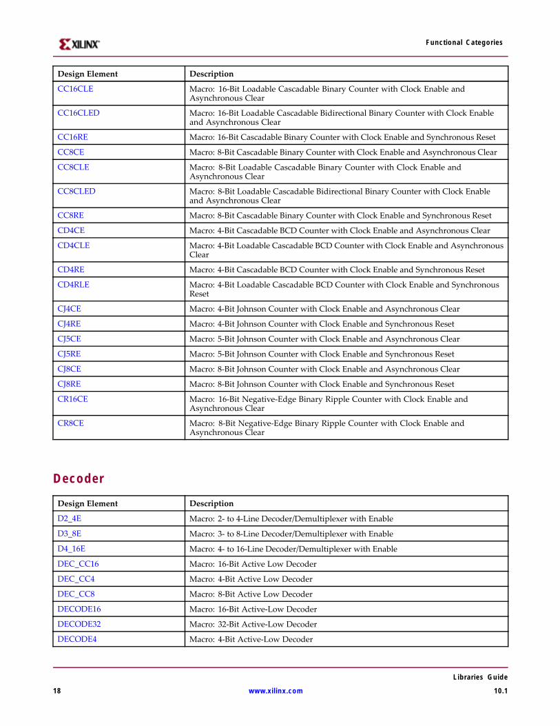
Functional Categories
Design Element Description
CC16CLE Macro: 16-Bit Loadable Cascadable Binary Counter with Clock Enable andAsynchronous Clear
CC16CLED Macro: 16-Bit Loadable Cascadable Bidirectional Binary Counter with Clock Enableand Asynchronous Clear
CC16RE Macro: 16-Bit Cascadable Binary Counter with Clock Enable and Synchronous Reset
CC8CE Macro: 8-Bit Cascadable Binary Counter with Clock Enable and Asynchronous Clear
CC8CLE Macro: 8-Bit Loadable Cascadable Binary Counter with Clock Enable andAsynchronous Clear
CC8CLED Macro: 8-Bit Loadable Cascadable Bidirectional Binary Counter with Clock Enableand Asynchronous Clear
CC8RE Macro: 8-Bit Cascadable Binary Counter with Clock Enable and Synchronous Reset
CD4CE Macro: 4-Bit Cascadable BCD Counter with Clock Enable and Asynchronous Clear
CD4CLE Macro: 4-Bit Loadable Cascadable BCD Counter with Clock Enable and AsynchronousClear
CD4RE Macro: 4-Bit Cascadable BCD Counter with Clock Enable and Synchronous Reset
CD4RLE Macro: 4-Bit Loadable Cascadable BCD Counter with Clock Enable and SynchronousReset
CJ4CE Macro: 4-Bit Johnson Counter with Clock Enable and Asynchronous Clear
CJ4RE Macro: 4-Bit Johnson Counter with Clock Enable and Synchronous Reset
CJ5CE Macro: 5-Bit Johnson Counter with Clock Enable and Asynchronous Clear
CJ5RE Macro: 5-Bit Johnson Counter with Clock Enable and Synchronous Reset
CJ8CE Macro: 8-Bit Johnson Counter with Clock Enable and Asynchronous Clear
CJ8RE Macro: 8-Bit Johnson Counter with Clock Enable and Synchronous Reset
CR16CE Macro: 16-Bit Negative-Edge Binary Ripple Counter with Clock Enable andAsynchronous Clear
CR8CE Macro: 8-Bit Negative-Edge Binary Ripple Counter with Clock Enable andAsynchronous Clear
Decoder
Design Element Description
D2_4E Macro: 2- to 4-Line Decoder/Demultiplexer with Enable
D3_8E Macro: 3- to 8-Line Decoder/Demultiplexer with Enable
D4_16E Macro: 4- to 16-Line Decoder/Demultiplexer with Enable
DEC_CC16 Macro: 16-Bit Active Low Decoder
DEC_CC4 Macro: 4-Bit Active Low Decoder
DEC_CC8 Macro: 8-Bit Active Low Decoder
DECODE16 Macro: 16-Bit Active-Low Decoder
DECODE32 Macro: 32-Bit Active-Low Decoder
DECODE4 Macro: 4-Bit Active-Low Decoder
Libraries Guide
18 www.xilinx.com 10.1
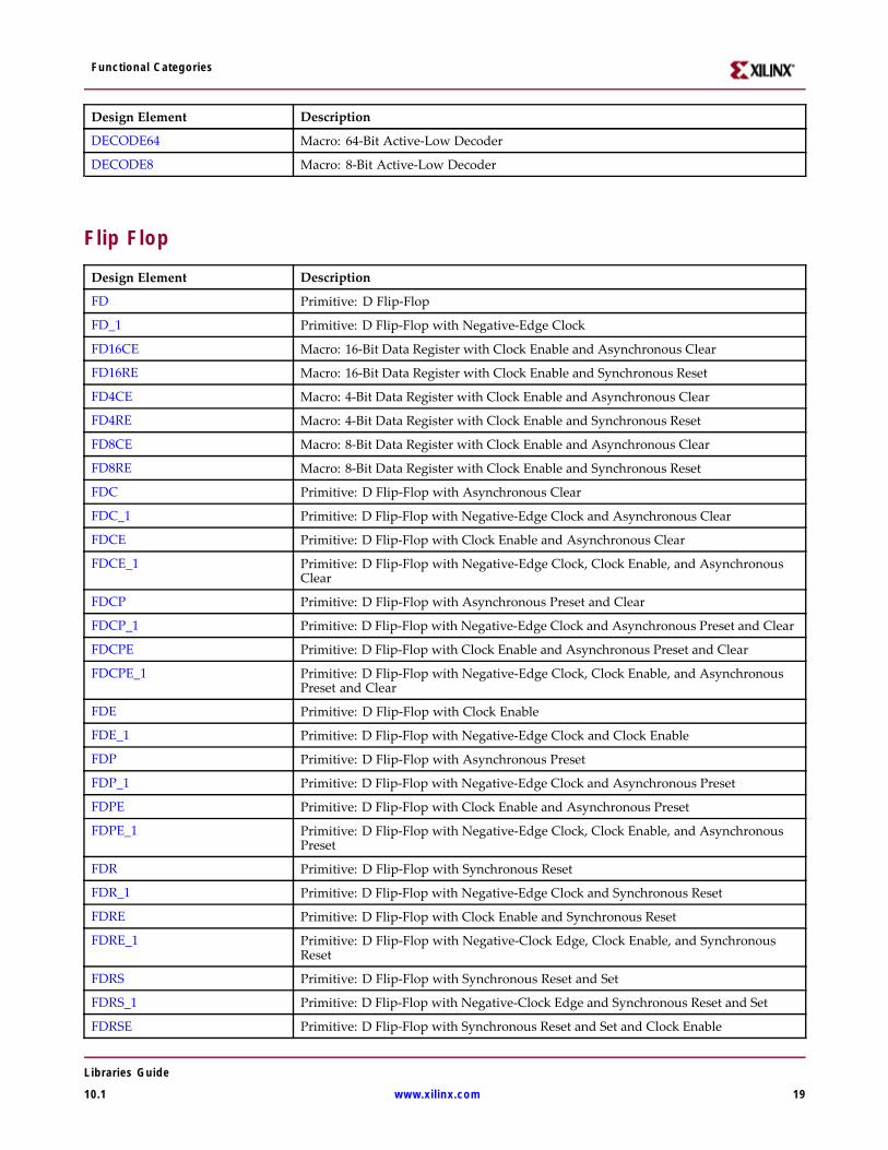
Functional Categories
Design Element Description
DECODE64 Macro: 64-Bit Active-Low Decoder
DECODE8 Macro: 8-Bit Active-Low Decoder
Flip Flop
Design Element Description
FD Primitive: D Flip-Flop
FD_1 Primitive: D Flip-Flop with Negative-Edge Clock
FD16CE Macro: 16-Bit Data Register with Clock Enable and Asynchronous Clear
FD16RE Macro: 16-Bit Data Register with Clock Enable and Synchronous Reset
FD4CE Macro: 4-Bit Data Register with Clock Enable and Asynchronous Clear
FD4RE Macro: 4-Bit Data Register with Clock Enable and Synchronous Reset
FD8CE Macro: 8-Bit Data Register with Clock Enable and Asynchronous Clear
FD8RE Macro: 8-Bit Data Register with Clock Enable and Synchronous Reset
FDC Primitive: D Flip-Flop with Asynchronous Clear
FDC_1 Primitive: D Flip-Flop with Negative-Edge Clock and Asynchronous Clear
FDCE Primitive: D Flip-Flop with Clock Enable and Asynchronous Clear
FDCE_1 Primitive: D Flip-Flop with Negative-Edge Clock, Clock Enable, and AsynchronousClear
FDCP Primitive: D Flip-Flop with Asynchronous Preset and Clear
FDCP_1 Primitive: D Flip-Flop with Negative-Edge Clock and Asynchronous Preset and Clear
FDCPE Primitive: D Flip-Flop with Clock Enable and Asynchronous Preset and Clear
FDCPE_1 Primitive: D Flip-Flop with Negative-Edge Clock, Clock Enable, and AsynchronousPreset and Clear
FDE Primitive: D Flip-Flop with Clock Enable
FDE_1 Primitive: D Flip-Flop with Negative-Edge Clock and Clock Enable
FDP Primitive: D Flip-Flop with Asynchronous Preset
FDP_1 Primitive: D Flip-Flop with Negative-Edge Clock and Asynchronous Preset
FDPE Primitive: D Flip-Flop with Clock Enable and Asynchronous Preset
FDPE_1 Primitive: D Flip-Flop with Negative-Edge Clock, Clock Enable, and AsynchronousPreset
FDR Primitive: D Flip-Flop with Synchronous Reset
FDR_1 Primitive: D Flip-Flop with Negative-Edge Clock and Synchronous Reset
FDRE Primitive: D Flip-Flop with Clock Enable and Synchronous Reset
FDRE_1 Primitive: D Flip-Flop with Negative-Clock Edge, Clock Enable, and SynchronousReset
FDRS Primitive: D Flip-Flop with Synchronous Reset and Set
FDRS_1 Primitive: D Flip-Flop with Negative-Clock Edge and Synchronous Reset and Set
FDRSE Primitive: D Flip-Flop with Synchronous Reset and Set and Clock Enable
Libraries Guide
10.1 www.xilinx.com 19
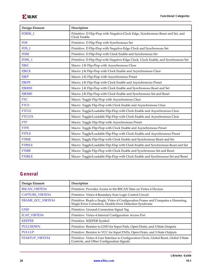
Functional Categories
Design Element Description
FDRSE_1 Primitive: D Flip-Flop with Negative-Clock Edge, Synchronous Reset and Set, andClock Enable
FDS Primitive: D Flip-Flop with Synchronous Set
FDS_1 Primitive: D Flip-Flop with Negative-Edge Clock and Synchronous Set
FDSE Primitive: D Flip-Flop with Clock Enable and Synchronous Set
FDSE_1 Primitive: D Flip-Flop with Negative-Edge Clock, Clock Enable, and Synchronous Set
FJKC Macro: J-K Flip-Flop with Asynchronous Clear
FJKCE Macro: J-K Flip-Flop with Clock Enable and Asynchronous Clear
FJKP Macro: J-K Flip-Flop with Asynchronous Preset
FJKPE Macro: J-K Flip-Flop with Clock Enable and Asynchronous Preset
FJKRSE Macro: J-K Flip-Flop with Clock Enable and Synchronous Reset and Set
FJKSRE Macro: J-K Flip-Flop with Clock Enable and Synchronous Set and Reset
FTC Macro: Toggle Flip-Flop with Asynchronous Clear
FTCE Macro: Toggle Flip-Flop with Clock Enable and Asynchronous Clear
FTCLE Macro: Toggle/Loadable Flip-Flop with Clock Enable and Asynchronous Clear
FTCLEX Macro: Toggle/Loadable Flip-Flop with Clock Enable and Asynchronous Clear
FTP Macro: Toggle Flip-Flop with Asynchronous Preset
FTPE Macro: Toggle Flip-Flop with Clock Enable and Asynchronous Preset
FTPLE Macro: Toggle/Loadable Flip-Flop with Clock Enable and Asynchronous Preset
FTRSE Macro: Toggle Flip-Flop with Clock Enable and Synchronous Reset and Set
FTRSLE Macro: Toggle/Loadable Flip-Flop with Clock Enable and Synchronous Reset and Set
FTSRE Macro: Toggle Flip-Flop with Clock Enable and Synchronous Set and Reset
FTSRLE Macro: Toggle/Loadable Flip-Flop with Clock Enable and Synchronous Set and Reset
General
Design Element Description
BSCAN_VIRTEX4 Primitive: Provides Access to the BSCAN Sites on Virtex-4 Devices
CAPTURE_VIRTEX4 Primitive: Virtex-4 Boundary Scan Logic Control Circuit
FRAME_ECC_VIRTEX4 Primitive: Reads a Single, Virtex-4 Configuration Frame and Computes a Hamming,Single-Error Correction, Double-Error Detection Syndrome
GND Primitive: Ground-Connection Signal Tag
ICAP_VIRTEX4 Primitive: Virtex-4 Internal Configuration Access Port
KEEPER Primitive: KEEPER Symbol
PULLDOWN Primitive: Resistor to GND for Input Pads, Open-Drain, and 3-State Outputs
PULLUP Primitive: Resistor to VCC for Input PADs, Open-Drain, and 3-State Outputs
STARTUP_VIRTEX4 Primitive: Virtex-4 User Interface to Configuration Clock, Global Reset, Global 3-StateControls, and Other Configuration Signals
Libraries Guide
20 www.xilinx.com 10.1
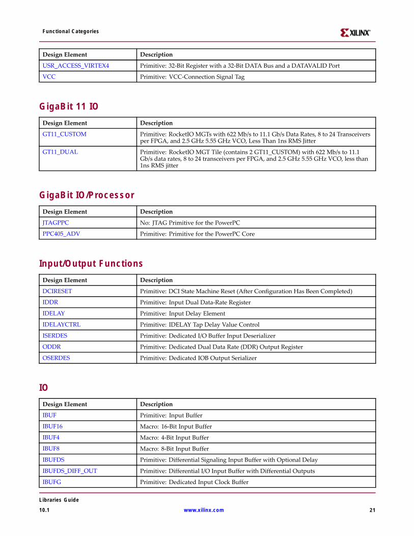
Functional Categories
Design Element Description
USR_ACCESS_VIRTEX4 Primitive: 32-Bit Register with a 32-Bit DATA Bus and a DATAVALID Port
VCC Primitive: VCC-Connection Signal Tag
GigaBit 11 IODesign Element Description
GT11_CUSTOM Primitive: RocketIO MGTs with 622 Mb/s to 11.1 Gb/s Data Rates, 8 to 24 Transceiversper FPGA, and 2.5 GHz 5.55 GHz VCO, Less Than 1ns RMS Jitter
GT11_DUAL Primitive: RocketIO MGT Tile (contains 2 GT11_CUSTOM) with 622 Mb/s to 11.1Gb/s data rates, 8 to 24 transceivers per FPGA, and 2.5 GHz 5.55 GHz VCO, less than1ns RMS jitter
GigaBit IO/ProcessorDesign Element Description
JTAGPPC No: JTAG Primitive for the PowerPC
PPC405_ADV Primitive: Primitive for the PowerPC Core
Input/Output FunctionsDesign Element Description
DCIRESET Primitive: DCI State Machine Reset (After Configuration Has Been Completed)
IDDR Primitive: Input Dual Data-Rate Register
IDELAY Primitive: Input Delay Element
IDELAYCTRL Primitive: IDELAY Tap Delay Value Control
ISERDES Primitive: Dedicated I/O Buffer Input Deserializer
ODDR Primitive: Dedicated Dual Data Rate (DDR) Output Register
OSERDES Primitive: Dedicated IOB Output Serializer
IODesign Element Description
IBUF Primitive: Input Buffer
IBUF16 Macro: 16-Bit Input Buffer
IBUF4 Macro: 4-Bit Input Buffer
IBUF8 Macro: 8-Bit Input Buffer
IBUFDS Primitive: Differential Signaling Input Buffer with Optional Delay
IBUFDS_DIFF_OUT Primitive: Differential I/O Input Buffer with Differential Outputs
IBUFG Primitive: Dedicated Input Clock Buffer
Libraries Guide
10.1 www.xilinx.com 21
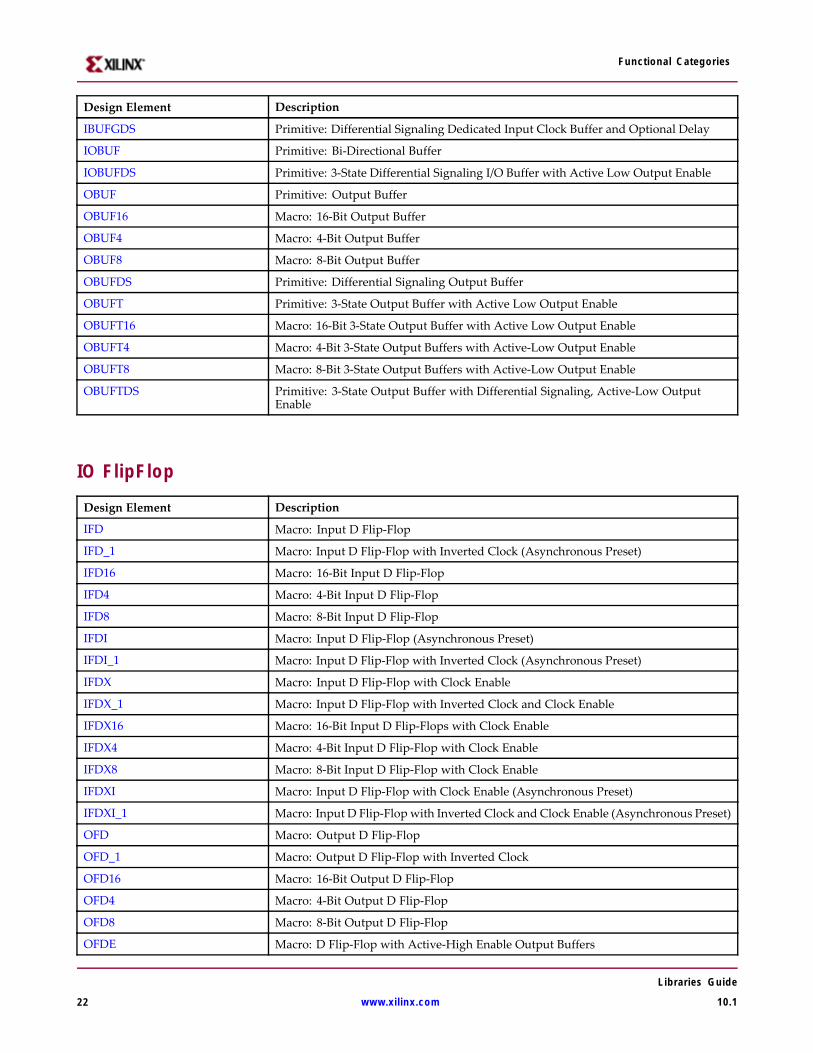
Functional Categories
Design Element Description
IBUFGDS Primitive: Differential Signaling Dedicated Input Clock Buffer and Optional Delay
IOBUF Primitive: Bi-Directional Buffer
IOBUFDS Primitive: 3-State Differential Signaling I/O Buffer with Active Low Output Enable
OBUF Primitive: Output Buffer
OBUF16 Macro: 16-Bit Output Buffer
OBUF4 Macro: 4-Bit Output Buffer
OBUF8 Macro: 8-Bit Output Buffer
OBUFDS Primitive: Differential Signaling Output Buffer
OBUFT Primitive: 3-State Output Buffer with Active Low Output Enable
OBUFT16 Macro: 16-Bit 3-State Output Buffer with Active Low Output Enable
OBUFT4 Macro: 4-Bit 3-State Output Buffers with Active-Low Output Enable
OBUFT8 Macro: 8-Bit 3-State Output Buffers with Active-Low Output Enable
OBUFTDS Primitive: 3-State Output Buffer with Differential Signaling, Active-Low OutputEnable
IO FlipFlop
Design Element Description
IFD Macro: Input D Flip-Flop
IFD_1 Macro: Input D Flip-Flop with Inverted Clock (Asynchronous Preset)
IFD16 Macro: 16-Bit Input D Flip-Flop
IFD4 Macro: 4-Bit Input D Flip-Flop
IFD8 Macro: 8-Bit Input D Flip-Flop
IFDI Macro: Input D Flip-Flop (Asynchronous Preset)
IFDI_1 Macro: Input D Flip-Flop with Inverted Clock (Asynchronous Preset)
IFDX Macro: Input D Flip-Flop with Clock Enable
IFDX_1 Macro: Input D Flip-Flop with Inverted Clock and Clock Enable
IFDX16 Macro: 16-Bit Input D Flip-Flops with Clock Enable
IFDX4 Macro: 4-Bit Input D Flip-Flop with Clock Enable
IFDX8 Macro: 8-Bit Input D Flip-Flop with Clock Enable
IFDXI Macro: Input D Flip-Flop with Clock Enable (Asynchronous Preset)
IFDXI_1 Macro: Input D Flip-Flop with Inverted Clock and Clock Enable (Asynchronous Preset)
OFD Macro: Output D Flip-Flop
OFD_1 Macro: Output D Flip-Flop with Inverted Clock
OFD16 Macro: 16-Bit Output D Flip-Flop
OFD4 Macro: 4-Bit Output D Flip-Flop
OFD8 Macro: 8-Bit Output D Flip-Flop
OFDE Macro: D Flip-Flop with Active-High Enable Output Buffers
Libraries Guide
22 www.xilinx.com 10.1
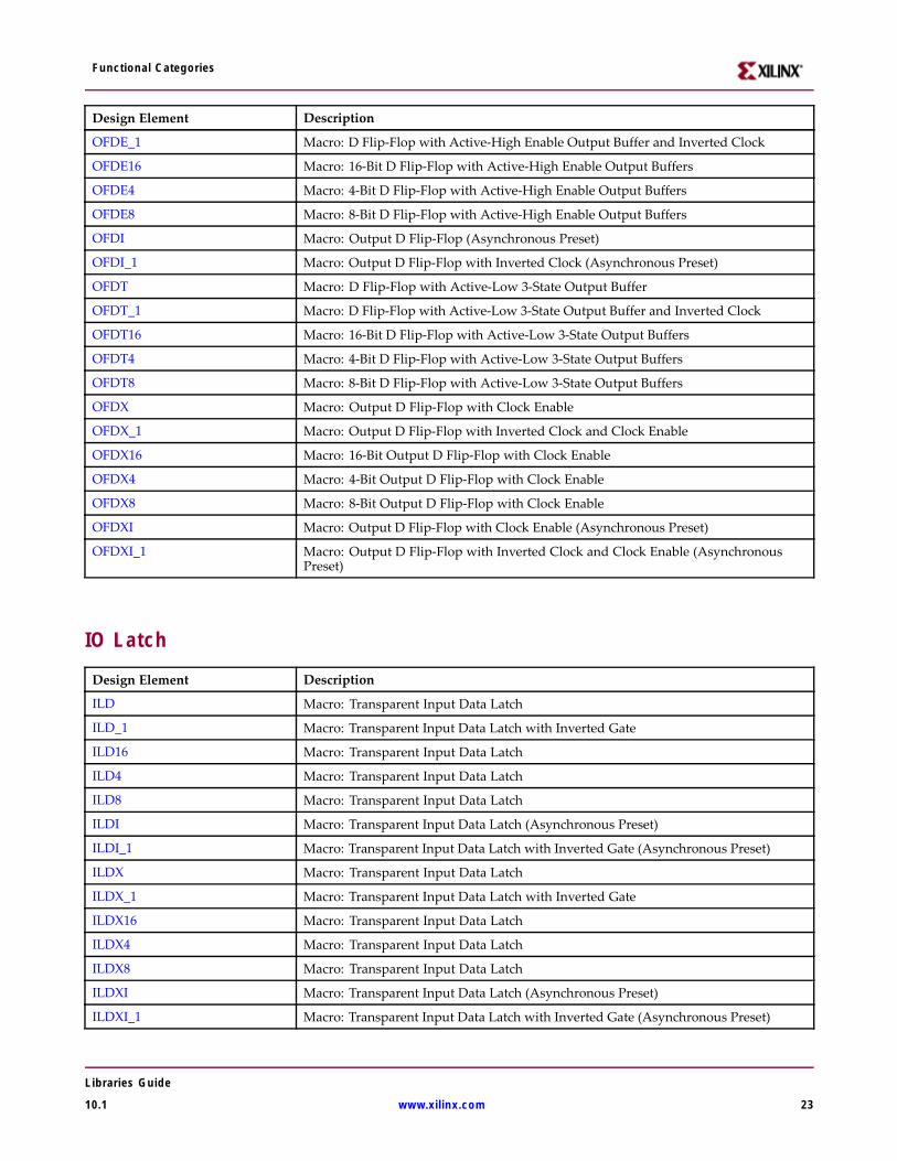
Functional Categories
Design Element Description
OFDE_1 Macro: D Flip-Flop with Active-High Enable Output Buffer and Inverted Clock
OFDE16 Macro: 16-Bit D Flip-Flop with Active-High Enable Output Buffers
OFDE4 Macro: 4-Bit D Flip-Flop with Active-High Enable Output Buffers
OFDE8 Macro: 8-Bit D Flip-Flop with Active-High Enable Output Buffers
OFDI Macro: Output D Flip-Flop (Asynchronous Preset)
OFDI_1 Macro: Output D Flip-Flop with Inverted Clock (Asynchronous Preset)
OFDT Macro: D Flip-Flop with Active-Low 3-State Output Buffer
OFDT_1 Macro: D Flip-Flop with Active-Low 3-State Output Buffer and Inverted Clock
OFDT16 Macro: 16-Bit D Flip-Flop with Active-Low 3-State Output Buffers
OFDT4 Macro: 4-Bit D Flip-Flop with Active-Low 3-State Output Buffers
OFDT8 Macro: 8-Bit D Flip-Flop with Active-Low 3-State Output Buffers
OFDX Macro: Output D Flip-Flop with Clock Enable
OFDX_1 Macro: Output D Flip-Flop with Inverted Clock and Clock Enable
OFDX16 Macro: 16-Bit Output D Flip-Flop with Clock Enable
OFDX4 Macro: 4-Bit Output D Flip-Flop with Clock Enable
OFDX8 Macro: 8-Bit Output D Flip-Flop with Clock Enable
OFDXI Macro: Output D Flip-Flop with Clock Enable (Asynchronous Preset)
OFDXI_1 Macro: Output D Flip-Flop with Inverted Clock and Clock Enable (AsynchronousPreset)
IO Latch
Design Element Description
ILD Macro: Transparent Input Data Latch
ILD_1 Macro: Transparent Input Data Latch with Inverted Gate
ILD16 Macro: Transparent Input Data Latch
ILD4 Macro: Transparent Input Data Latch
ILD8 Macro: Transparent Input Data Latch
ILDI Macro: Transparent Input Data Latch (Asynchronous Preset)
ILDI_1 Macro: Transparent Input Data Latch with Inverted Gate (Asynchronous Preset)
ILDX Macro: Transparent Input Data Latch
ILDX_1 Macro: Transparent Input Data Latch with Inverted Gate
ILDX16 Macro: Transparent Input Data Latch
ILDX4 Macro: Transparent Input Data Latch
ILDX8 Macro: Transparent Input Data Latch
ILDXI Macro: Transparent Input Data Latch (Asynchronous Preset)
ILDXI_1 Macro: Transparent Input Data Latch with Inverted Gate (Asynchronous Preset)
Libraries Guide
10.1 www.xilinx.com 23
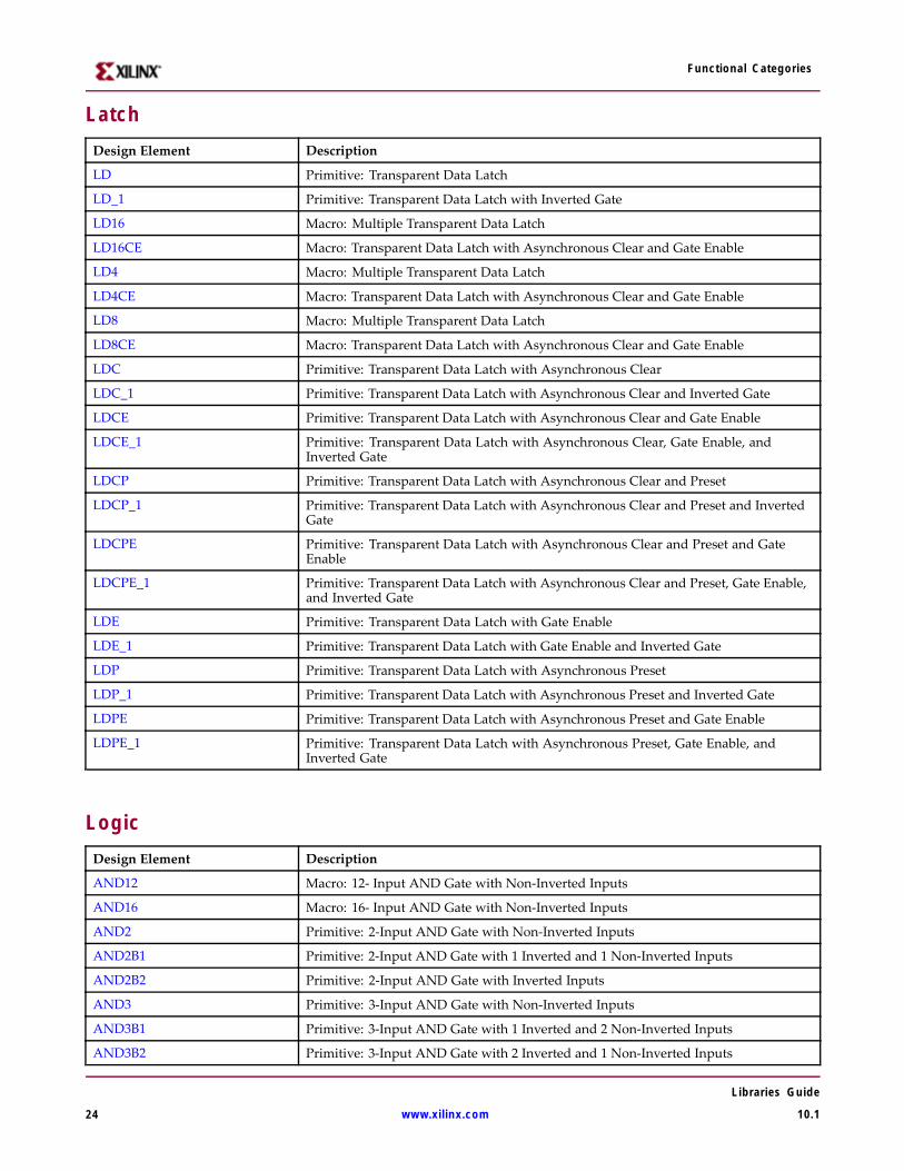
Functional Categories
LatchDesign Element Description
LD Primitive: Transparent Data Latch
LD_1 Primitive: Transparent Data Latch with Inverted Gate
LD16 Macro: Multiple Transparent Data Latch
LD16CE Macro: Transparent Data Latch with Asynchronous Clear and Gate Enable
LD4 Macro: Multiple Transparent Data Latch
LD4CE Macro: Transparent Data Latch with Asynchronous Clear and Gate Enable
LD8 Macro: Multiple Transparent Data Latch
LD8CE Macro: Transparent Data Latch with Asynchronous Clear and Gate Enable
LDC Primitive: Transparent Data Latch with Asynchronous Clear
LDC_1 Primitive: Transparent Data Latch with Asynchronous Clear and Inverted Gate
LDCE Primitive: Transparent Data Latch with Asynchronous Clear and Gate Enable
LDCE_1 Primitive: Transparent Data Latch with Asynchronous Clear, Gate Enable, andInverted Gate
LDCP Primitive: Transparent Data Latch with Asynchronous Clear and Preset
LDCP_1 Primitive: Transparent Data Latch with Asynchronous Clear and Preset and InvertedGate
LDCPE Primitive: Transparent Data Latch with Asynchronous Clear and Preset and GateEnable
LDCPE_1 Primitive: Transparent Data Latch with Asynchronous Clear and Preset, Gate Enable,and Inverted Gate
LDE Primitive: Transparent Data Latch with Gate Enable
LDE_1 Primitive: Transparent Data Latch with Gate Enable and Inverted Gate
LDP Primitive: Transparent Data Latch with Asynchronous Preset
LDP_1 Primitive: Transparent Data Latch with Asynchronous Preset and Inverted Gate
LDPE Primitive: Transparent Data Latch with Asynchronous Preset and Gate Enable
LDPE_1 Primitive: Transparent Data Latch with Asynchronous Preset, Gate Enable, andInverted Gate
LogicDesign Element Description
AND12 Macro: 12- Input AND Gate with Non-Inverted Inputs
AND16 Macro: 16- Input AND Gate with Non-Inverted Inputs
AND2 Primitive: 2-Input AND Gate with Non-Inverted Inputs
AND2B1 Primitive: 2-Input AND Gate with 1 Inverted and 1 Non-Inverted Inputs
AND2B2 Primitive: 2-Input AND Gate with Inverted Inputs
AND3 Primitive: 3-Input AND Gate with Non-Inverted Inputs
AND3B1 Primitive: 3-Input AND Gate with 1 Inverted and 2 Non-Inverted Inputs
AND3B2 Primitive: 3-Input AND Gate with 2 Inverted and 1 Non-Inverted Inputs
Libraries Guide
24 www.xilinx.com 10.1
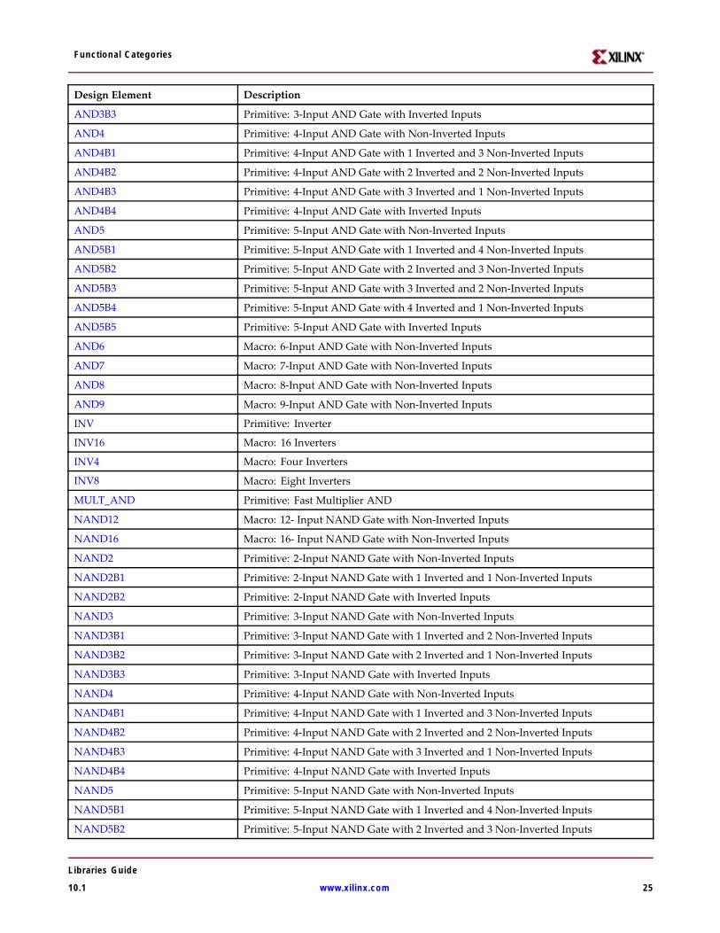
Functional Categories
Design Element Description
AND3B3 Primitive: 3-Input AND Gate with Inverted Inputs
AND4 Primitive: 4-Input AND Gate with Non-Inverted Inputs
AND4B1 Primitive: 4-Input AND Gate with 1 Inverted and 3 Non-Inverted Inputs
AND4B2 Primitive: 4-Input AND Gate with 2 Inverted and 2 Non-Inverted Inputs
AND4B3 Primitive: 4-Input AND Gate with 3 Inverted and 1 Non-Inverted Inputs
AND4B4 Primitive: 4-Input AND Gate with Inverted Inputs
AND5 Primitive: 5-Input AND Gate with Non-Inverted Inputs
AND5B1 Primitive: 5-Input AND Gate with 1 Inverted and 4 Non-Inverted Inputs
AND5B2 Primitive: 5-Input AND Gate with 2 Inverted and 3 Non-Inverted Inputs
AND5B3 Primitive: 5-Input AND Gate with 3 Inverted and 2 Non-Inverted Inputs
AND5B4 Primitive: 5-Input AND Gate with 4 Inverted and 1 Non-Inverted Inputs
AND5B5 Primitive: 5-Input AND Gate with Inverted Inputs
AND6 Macro: 6-Input AND Gate with Non-Inverted Inputs
AND7 Macro: 7-Input AND Gate with Non-Inverted Inputs
AND8 Macro: 8-Input AND Gate with Non-Inverted Inputs
AND9 Macro: 9-Input AND Gate with Non-Inverted Inputs
INV Primitive: Inverter
INV16 Macro: 16 Inverters
INV4 Macro: Four Inverters
INV8 Macro: Eight Inverters
MULT_AND Primitive: Fast Multiplier AND
NAND12 Macro: 12- Input NAND Gate with Non-Inverted Inputs
NAND16 Macro: 16- Input NAND Gate with Non-Inverted Inputs
NAND2 Primitive: 2-Input NAND Gate with Non-Inverted Inputs
NAND2B1 Primitive: 2-Input NAND Gate with 1 Inverted and 1 Non-Inverted Inputs
NAND2B2 Primitive: 2-Input NAND Gate with Inverted Inputs
NAND3 Primitive: 3-Input NAND Gate with Non-Inverted Inputs
NAND3B1 Primitive: 3-Input NAND Gate with 1 Inverted and 2 Non-Inverted Inputs
NAND3B2 Primitive: 3-Input NAND Gate with 2 Inverted and 1 Non-Inverted Inputs
NAND3B3 Primitive: 3-Input NAND Gate with Inverted Inputs
NAND4 Primitive: 4-Input NAND Gate with Non-Inverted Inputs
NAND4B1 Primitive: 4-Input NAND Gate with 1 Inverted and 3 Non-Inverted Inputs
NAND4B2 Primitive: 4-Input NAND Gate with 2 Inverted and 2 Non-Inverted Inputs
NAND4B3 Primitive: 4-Input NAND Gate with 3 Inverted and 1 Non-Inverted Inputs
NAND4B4 Primitive: 4-Input NAND Gate with Inverted Inputs
NAND5 Primitive: 5-Input NAND Gate with Non-Inverted Inputs
NAND5B1 Primitive: 5-Input NAND Gate with 1 Inverted and 4 Non-Inverted Inputs
NAND5B2 Primitive: 5-Input NAND Gate with 2 Inverted and 3 Non-Inverted Inputs
Libraries Guide
10.1 www.xilinx.com 25

Functional Categories
Design Element Description
NAND5B3 Primitive: 5-Input NAND Gate with 3 Inverted and 2 Non-Inverted Inputs
NAND5B4 Primitive: 5-Input NAND Gate with 4 Inverted and 1 Non-Inverted Inputs
NAND5B5 Primitive: 5-Input NAND Gate with Inverted Inputs
NAND6 Macro: 6-Input NAND Gate with Non-Inverted Inputs
NAND7 Macro: 7-Input NAND Gate with Non-Inverted Inputs
NAND8 Macro: 8-Input NAND Gate with Non-Inverted Inputs
NAND9 Macro: 9-Input NAND Gate with Non-Inverted Inputs
NOR12 Macro: 12-Input NOR Gate with Non-Inverted Inputs
NOR16 Macro: 16-Input NOR Gate with Non-Inverted Inputs
NOR2 Primitive: 2-Input NOR Gate with Non-Inverted Inputs
NOR2B1 Primitive: 2-Input NOR Gate with 1 Inverted and 1 Non-Inverted Inputs
NOR2B2 Primitive: 2-Input NOR Gate with Inverted Inputs
NOR3 Primitive: 3-Input NOR Gate with Non-Inverted Inputs
NOR3B1 Primitive: 3-Input NOR Gate with 1 Inverted and 2 Non-Inverted Inputs
NOR3B2 Primitive: 3-Input NOR Gate with 2 Inverted and 1 Non-Inverted Inputs
NOR3B3 Primitive: 3-Input NOR Gate with Inverted Inputs
NOR4 Primitive: 4-Input NOR Gate with Non-Inverted Inputs
NOR4B1 Primitive: 4-Input NOR Gate with 1 Inverted and 3 Non-Inverted Inputs
NOR4B2 Primitive: 4-Input NOR Gate with 2 Inverted and 2 Non-Inverted Inputs
NOR4B3 Primitive: 4-Input NOR Gate with 3 Inverted and 1 Non-Inverted Inputs
NOR4B4 Primitive: 4-Input NOR Gate with Inverted Inputs
NOR5 Primitive: 5-Input NOR Gate with Non-Inverted Inputs
NOR5B1 Primitive: 5-Input NOR Gate with 1 Inverted and 4 Non-Inverted Inputs
NOR5B2 Primitive: 5-Input NOR Gate with 2 Inverted and 3 Non-Inverted Inputs
NOR5B3 Primitive: 5-Input NOR Gate with 3 Inverted and 2 Non-Inverted Inputs
NOR5B4 Primitive: 5-Input NOR Gate with 4 Inverted and 1 Non-Inverted Inputs
NOR5B5 Primitive: 5-Input NOR Gate with Inverted Inputs
NOR6 Macro: 6-Input NOR Gate with Non-Inverted Inputs
NOR7 Macro: 7-Input NOR Gate with Non-Inverted Inputs
NOR8 Macro: 8-Input NOR Gate with Non-Inverted Inputs
NOR9 Macro: 9-Input NOR Gate with Non-Inverted Inputs
OR12 Macro: 12-Input OR Gate with Non-Inverted Inputs
OR16 Macro: 16-Input OR Gate with Non-Inverted Inputs
OR2 Primitive: 2-Input OR Gate with Non-Inverted Inputs
OR2B1 Primitive: 2-Input OR Gate with 1 Inverted and 1 Non-Inverted Inputs
OR2B2 Primitive: 2-Input OR Gate with Inverted Inputs
OR3 Primitive: 3-Input OR Gate with Non-Inverted Inputs
OR3B1 Primitive: 3-Input OR Gate with 1 Inverted and 2 Non-Inverted Inputs
Libraries Guide
26 www.xilinx.com 10.1
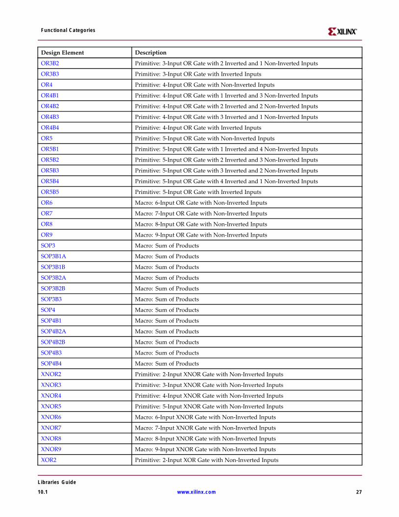
Functional Categories
Design Element Description
OR3B2 Primitive: 3-Input OR Gate with 2 Inverted and 1 Non-Inverted Inputs
OR3B3 Primitive: 3-Input OR Gate with Inverted Inputs
OR4 Primitive: 4-Input OR Gate with Non-Inverted Inputs
OR4B1 Primitive: 4-Input OR Gate with 1 Inverted and 3 Non-Inverted Inputs
OR4B2 Primitive: 4-Input OR Gate with 2 Inverted and 2 Non-Inverted Inputs
OR4B3 Primitive: 4-Input OR Gate with 3 Inverted and 1 Non-Inverted Inputs
OR4B4 Primitive: 4-Input OR Gate with Inverted Inputs
OR5 Primitive: 5-Input OR Gate with Non-Inverted Inputs
OR5B1 Primitive: 5-Input OR Gate with 1 Inverted and 4 Non-Inverted Inputs
OR5B2 Primitive: 5-Input OR Gate with 2 Inverted and 3 Non-Inverted Inputs
OR5B3 Primitive: 5-Input OR Gate with 3 Inverted and 2 Non-Inverted Inputs
OR5B4 Primitive: 5-Input OR Gate with 4 Inverted and 1 Non-Inverted Inputs
OR5B5 Primitive: 5-Input OR Gate with Inverted Inputs
OR6 Macro: 6-Input OR Gate with Non-Inverted Inputs
OR7 Macro: 7-Input OR Gate with Non-Inverted Inputs
OR8 Macro: 8-Input OR Gate with Non-Inverted Inputs
OR9 Macro: 9-Input OR Gate with Non-Inverted Inputs
SOP3 Macro: Sum of Products
SOP3B1A Macro: Sum of Products
SOP3B1B Macro: Sum of Products
SOP3B2A Macro: Sum of Products
SOP3B2B Macro: Sum of Products
SOP3B3 Macro: Sum of Products
SOP4 Macro: Sum of Products
SOP4B1 Macro: Sum of Products
SOP4B2A Macro: Sum of Products
SOP4B2B Macro: Sum of Products
SOP4B3 Macro: Sum of Products
SOP4B4 Macro: Sum of Products
XNOR2 Primitive: 2-Input XNOR Gate with Non-Inverted Inputs
XNOR3 Primitive: 3-Input XNOR Gate with Non-Inverted Inputs
XNOR4 Primitive: 4-Input XNOR Gate with Non-Inverted Inputs
XNOR5 Primitive: 5-Input XNOR Gate with Non-Inverted Inputs
XNOR6 Macro: 6-Input XNOR Gate with Non-Inverted Inputs
XNOR7 Macro: 7-Input XNOR Gate with Non-Inverted Inputs
XNOR8 Macro: 8-Input XNOR Gate with Non-Inverted Inputs
XNOR9 Macro: 9-Input XNOR Gate with Non-Inverted Inputs
XOR2 Primitive: 2-Input XOR Gate with Non-Inverted Inputs
Libraries Guide
10.1 www.xilinx.com 27
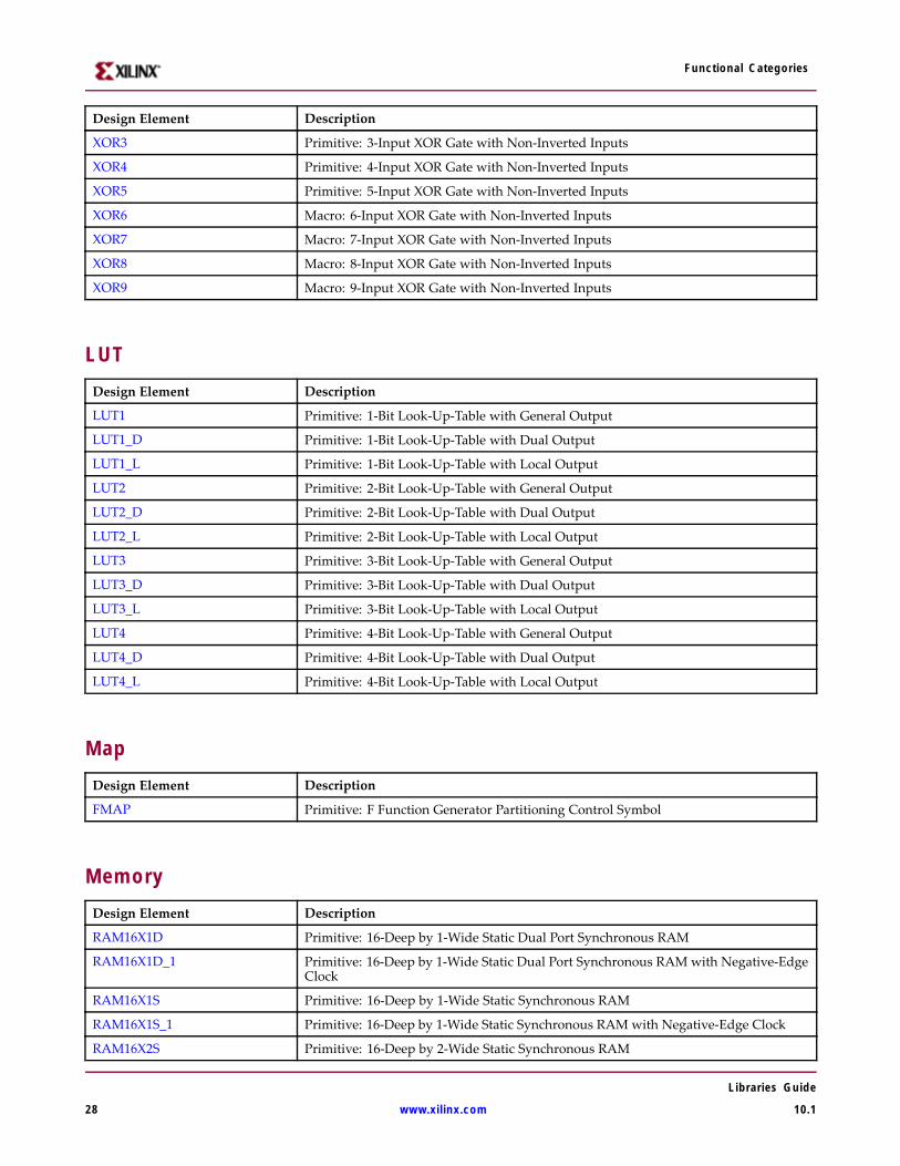
Functional Categories
Design Element Description
XOR3 Primitive: 3-Input XOR Gate with Non-Inverted Inputs
XOR4 Primitive: 4-Input XOR Gate with Non-Inverted Inputs
XOR5 Primitive: 5-Input XOR Gate with Non-Inverted Inputs
XOR6 Macro: 6-Input XOR Gate with Non-Inverted Inputs
XOR7 Macro: 7-Input XOR Gate with Non-Inverted Inputs
XOR8 Macro: 8-Input XOR Gate with Non-Inverted Inputs
XOR9 Macro: 9-Input XOR Gate with Non-Inverted Inputs
LUTDesign Element Description
LUT1 Primitive: 1-Bit Look-Up-Table with General Output
LUT1_D Primitive: 1-Bit Look-Up-Table with Dual Output
LUT1_L Primitive: 1-Bit Look-Up-Table with Local Output
LUT2 Primitive: 2-Bit Look-Up-Table with General Output
LUT2_D Primitive: 2-Bit Look-Up-Table with Dual Output
LUT2_L Primitive: 2-Bit Look-Up-Table with Local Output
LUT3 Primitive: 3-Bit Look-Up-Table with General Output
LUT3_D Primitive: 3-Bit Look-Up-Table with Dual Output
LUT3_L Primitive: 3-Bit Look-Up-Table with Local Output
LUT4 Primitive: 4-Bit Look-Up-Table with General Output
LUT4_D Primitive: 4-Bit Look-Up-Table with Dual Output
LUT4_L Primitive: 4-Bit Look-Up-Table with Local Output
MapDesign Element Description
FMAP Primitive: F Function Generator Partitioning Control Symbol
MemoryDesign Element Description
RAM16X1D Primitive: 16-Deep by 1-Wide Static Dual Port Synchronous RAM
RAM16X1D_1 Primitive: 16-Deep by 1-Wide Static Dual Port Synchronous RAM with Negative-EdgeClock
RAM16X1S Primitive: 16-Deep by 1-Wide Static Synchronous RAM
RAM16X1S_1 Primitive: 16-Deep by 1-Wide Static Synchronous RAM with Negative-Edge Clock
RAM16X2S Primitive: 16-Deep by 2-Wide Static Synchronous RAM
Libraries Guide
28 www.xilinx.com 10.1
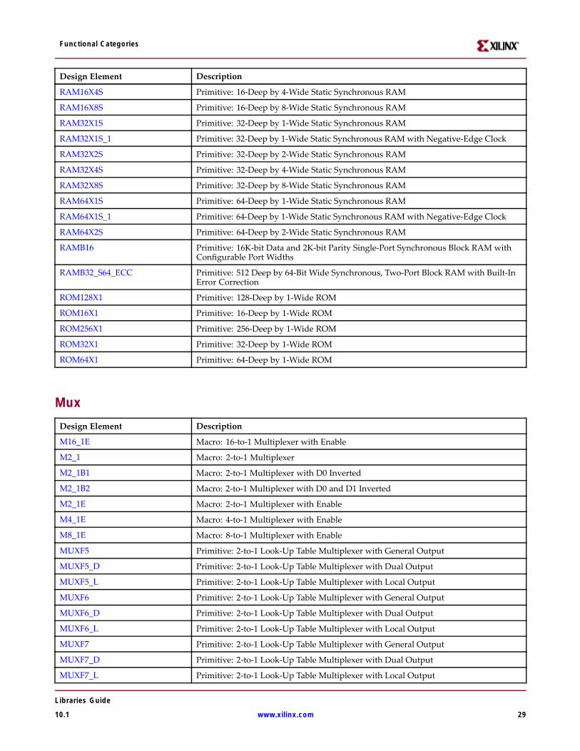
Functional Categories
Design Element Description
RAM16X4S Primitive: 16-Deep by 4-Wide Static Synchronous RAM
RAM16X8S Primitive: 16-Deep by 8-Wide Static Synchronous RAM
RAM32X1S Primitive: 32-Deep by 1-Wide Static Synchronous RAM
RAM32X1S_1 Primitive: 32-Deep by 1-Wide Static Synchronous RAM with Negative-Edge Clock
RAM32X2S Primitive: 32-Deep by 2-Wide Static Synchronous RAM
RAM32X4S Primitive: 32-Deep by 4-Wide Static Synchronous RAM
RAM32X8S Primitive: 32-Deep by 8-Wide Static Synchronous RAM
RAM64X1S Primitive: 64-Deep by 1-Wide Static Synchronous RAM
RAM64X1S_1 Primitive: 64-Deep by 1-Wide Static Synchronous RAM with Negative-Edge Clock
RAM64X2S Primitive: 64-Deep by 2-Wide Static Synchronous RAM
RAMB16 Primitive: 16K-bit Data and 2K-bit Parity Single-Port Synchronous Block RAM withConfigurable Port Widths
RAMB32_S64_ECC Primitive: 512 Deep by 64-Bit Wide Synchronous, Two-Port Block RAM with Built-InError Correction
ROM128X1 Primitive: 128-Deep by 1-Wide ROM
ROM16X1 Primitive: 16-Deep by 1-Wide ROM
ROM256X1 Primitive: 256-Deep by 1-Wide ROM
ROM32X1 Primitive: 32-Deep by 1-Wide ROM
ROM64X1 Primitive: 64-Deep by 1-Wide ROM
MuxDesign Element Description
M16_1E Macro: 16-to-1 Multiplexer with Enable
M2_1 Macro: 2-to-1 Multiplexer
M2_1B1 Macro: 2-to-1 Multiplexer with D0 Inverted
M2_1B2 Macro: 2-to-1 Multiplexer with D0 and D1 Inverted
M2_1E Macro: 2-to-1 Multiplexer with Enable
M4_1E Macro: 4-to-1 Multiplexer with Enable
M8_1E Macro: 8-to-1 Multiplexer with Enable
MUXF5 Primitive: 2-to-1 Look-Up Table Multiplexer with General Output
MUXF5_D Primitive: 2-to-1 Look-Up Table Multiplexer with Dual Output
MUXF5_L Primitive: 2-to-1 Look-Up Table Multiplexer with Local Output
MUXF6 Primitive: 2-to-1 Look-Up Table Multiplexer with General Output
MUXF6_D Primitive: 2-to-1 Look-Up Table Multiplexer with Dual Output
MUXF6_L Primitive: 2-to-1 Look-Up Table Multiplexer with Local Output
MUXF7 Primitive: 2-to-1 Look-Up Table Multiplexer with General Output
MUXF7_D Primitive: 2-to-1 Look-Up Table Multiplexer with Dual Output
MUXF7_L Primitive: 2-to-1 Look-Up Table Multiplexer with Local Output
Libraries Guide
10.1 www.xilinx.com 29
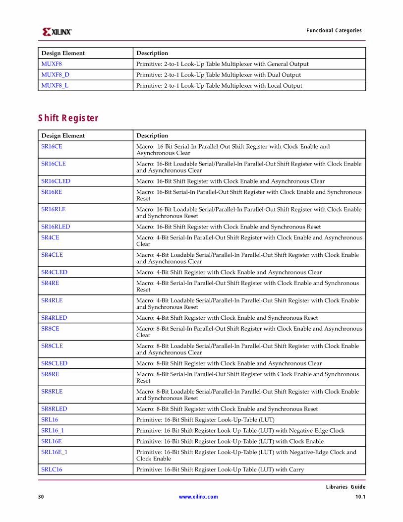
Functional Categories
Design Element Description
MUXF8 Primitive: 2-to-1 Look-Up Table Multiplexer with General Output
MUXF8_D Primitive: 2-to-1 Look-Up Table Multiplexer with Dual Output
MUXF8_L Primitive: 2-to-1 Look-Up Table Multiplexer with Local Output
Shift Register
Design Element Description
SR16CE Macro: 16-Bit Serial-In Parallel-Out Shift Register with Clock Enable andAsynchronous Clear
SR16CLE Macro: 16-Bit Loadable Serial/Parallel-In Parallel-Out Shift Register with Clock Enableand Asynchronous Clear
SR16CLED Macro: 16-Bit Shift Register with Clock Enable and Asynchronous Clear
SR16RE Macro: 16-Bit Serial-In Parallel-Out Shift Register with Clock Enable and SynchronousReset
SR16RLE Macro: 16-Bit Loadable Serial/Parallel-In Parallel-Out Shift Register with Clock Enableand Synchronous Reset
SR16RLED Macro: 16-Bit Shift Register with Clock Enable and Synchronous Reset
SR4CE Macro: 4-Bit Serial-In Parallel-Out Shift Register with Clock Enable and AsynchronousClear
SR4CLE Macro: 4-Bit Loadable Serial/Parallel-In Parallel-Out Shift Register with Clock Enableand Asynchronous Clear
SR4CLED Macro: 4-Bit Shift Register with Clock Enable and Asynchronous Clear
SR4RE Macro: 4-Bit Serial-In Parallel-Out Shift Register with Clock Enable and SynchronousReset
SR4RLE Macro: 4-Bit Loadable Serial/Parallel-In Parallel-Out Shift Register with Clock Enableand Synchronous Reset
SR4RLED Macro: 4-Bit Shift Register with Clock Enable and Synchronous Reset
SR8CE Macro: 8-Bit Serial-In Parallel-Out Shift Register with Clock Enable and AsynchronousClear
SR8CLE Macro: 8-Bit Loadable Serial/Parallel-In Parallel-Out Shift Register with Clock Enableand Asynchronous Clear
SR8CLED Macro: 8-Bit Shift Register with Clock Enable and Asynchronous Clear
SR8RE Macro: 8-Bit Serial-In Parallel-Out Shift Register with Clock Enable and SynchronousReset
SR8RLE Macro: 8-Bit Loadable Serial/Parallel-In Parallel-Out Shift Register with Clock Enableand Synchronous Reset
SR8RLED Macro: 8-Bit Shift Register with Clock Enable and Synchronous Reset
SRL16 Primitive: 16-Bit Shift Register Look-Up-Table (LUT)
SRL16_1 Primitive: 16-Bit Shift Register Look-Up-Table (LUT) with Negative-Edge Clock
SRL16E Primitive: 16-Bit Shift Register Look-Up-Table (LUT) with Clock Enable
SRL16E_1 Primitive: 16-Bit Shift Register Look-Up-Table (LUT) with Negative-Edge Clock andClock Enable
SRLC16 Primitive: 16-Bit Shift Register Look-Up Table (LUT) with Carry
Libraries Guide
30 www.xilinx.com 10.1
Functional Categories
Design Element Description
SRLC16_1 Primitive: 16-Bit Shift Register Look-Up Table (LUT) with Carry and Negative-EdgeClock
SRLC16E Primitive: 16-Bit Shift Register Look-Up Table (LUT) with Carry and Clock Enable
SRLC16E_1 Primitive: 16-Bit Shift Register Look-Up Table (LUT) with Carry, Negative-Edge Clock,and Clock Enable
Shifter
Design Element Description
BRLSHFT4 Macro: 4-Bit Barrel Shifter
BRLSHFT8 Macro: 8-Bit Barrel Shifter
Libraries Guide
10.1 www.xilinx.com 31

Libraries Guide
32 www.xilinx.com 10.1
About Design ElementsThis section describes the design elements that can be used with this architecture. The design elements areorganized alphabetically.
The following information is provided for each design element, where applicable:
• Name of element
• Brief description
• Schematic symbol (if any)
• Logic Table (if any)
• Port Descriptions (if any)
• Design Entry Method
• Available Attributes (if any)
• For more information
You can find examples of VHDL and Verilog instantiation code in the ISE software (in the main menu, select Edit> Language Templates or in the Libraries Guide for HDL Designs for this architecture.
Libraries Guide
10.1 www.xilinx.com 33
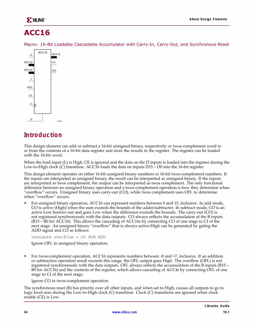
About Design Elements
ACC16Macro: 16-Bit Loadable Cascadable Accumulator with Carry-In, Carry-Out, and Synchronous Reset
IntroductionThis design element can add or subtract a 16-bit unsigned-binary, respectively or twos-complement word toor from the contents of a 16-bit data register and store the results in the register. The register can be loadedwith the 16-bit word.
When the load input (L) is High, CE is ignored and the data on the D inputs is loaded into the register during theLow-to-High clock (C) transition. ACC16 loads the data on inputs D15 – D0 into the 16-bit register.
This design element operates on either 16-bit unsigned binary numbers or 16-bit twos-complement numbers. Ifthe inputs are interpreted as unsigned binary, the result can be interpreted as unsigned binary. If the inputsare interpreted as twos complement, the output can be interpreted as twos complement. The only functionaldifference between an unsigned binary operation and a twos-complement operation is how they determine when“overflow” occurs. Unsigned binary uses carry-out (CO), while twos complement uses OFL to determinewhen “overflow” occurs.• For unsigned binary operation, ACC16 can represent numbers between 0 and 15, inclusive. In add mode,
CO is active (High) when the sum exceeds the bounds of the adder/subtracter. In subtract mode, CO is anactive-Low borrow-out and goes Low when the difference exceeds the bounds. The carry-out (CO) isnot registered synchronously with the data outputs. CO always reflects the accumulation of the B inputs(B15 – B0 for ACC16). This allows the cascading of ACC16s by connecting CO of one stage to CI of thenext stage. An unsigned binary “overflow” that is always active-High can be generated by gating theADD signal and CO as follows:unsigned overflow = CO XOR ADD
Ignore OFL in unsigned binary operation.
• For twos-complement operation, ACC16 represents numbers between -8 and +7, inclusive. If an additionor subtraction operation result exceeds this range, the OFL output goes High. The overflow (OFL) is notregistered synchronously with the data outputs. OFL always reflects the accumulation of the B inputs (B15 –B0 for ACC16) and the contents of the register, which allows cascading of ACC4s by connecting OFL of onestage to CI of the next stage.Ignore CO in twos-complement operation.
The synchronous reset (R) has priority over all other inputs, and when set to High, causes all outputs to go tologic level zero during the Low-to-High clock (C) transition. Clock (C) transitions are ignored when clockenable (CE) is Low.
Libraries Guide
34 www.xilinx.com 10.1
About Design Elements
This design element is asynchronously cleared, outputs Low, when power is applied. For FPGA devices,power-on conditions are simulated when global set/reset (GSR) is active. GSR defaults to active-High but can beinverted by adding an inverter in front of the GSR input of the appropriate STARTUP_architecture symbol.
Logic TableInput Output
R L CE ADD D C Q
1 x x x x ↑ 0
0 1 x x Dn ↑ Dn
0 0 1 1 x ↑ Q0+Bn+CI
0 0 1 0 x ↑ Q0-Bn-CI
0 0 0 x x ↑ No Change
Q0: Previous value of Q
Bn: Value of Data input B
CI: Value of input CI
Design Entry MethodThis design element is only for use in schematics.
For More Information• See the Virtex-4 User Guide.
• See the Virtex-4 Data Sheets.
Libraries Guide
10.1 www.xilinx.com 35
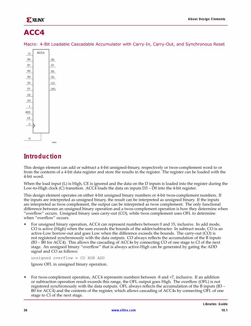
About Design Elements
ACC4Macro: 4-Bit Loadable Cascadable Accumulator with Carry-In, Carry-Out, and Synchronous Reset
IntroductionThis design element can add or subtract a 4-bit unsigned-binary, respectively or twos-complement word to orfrom the contents of a 4-bit data register and store the results in the register. The register can be loaded with the4-bit word.
When the load input (L) is High, CE is ignored and the data on the D inputs is loaded into the register during theLow-to-High clock (C) transition. ACC4 loads the data on inputs D3 – D0 into the 4-bit register.
This design element operates on either 4-bit unsigned binary numbers or 4-bit twos-complement numbers. Ifthe inputs are interpreted as unsigned binary, the result can be interpreted as unsigned binary. If the inputsare interpreted as twos complement, the output can be interpreted as twos complement. The only functionaldifference between an unsigned binary operation and a twos-complement operation is how they determine when“overflow” occurs. Unsigned binary uses carry-out (CO), while twos complement uses OFL to determinewhen “overflow” occurs.• For unsigned binary operation, ACC4 can represent numbers between 0 and 15, inclusive. In add mode,
CO is active (High) when the sum exceeds the bounds of the adder/subtracter. In subtract mode, CO is anactive-Low borrow-out and goes Low when the difference exceeds the bounds. The carry-out (CO) isnot registered synchronously with the data outputs. CO always reflects the accumulation of the B inputs(B3 – B0 for ACC4). This allows the cascading of ACC4s by connecting CO of one stage to CI of the nextstage. An unsigned binary “overflow” that is always active-High can be generated by gating the ADDsignal and CO as follows:unsigned overflow = CO XOR ADD
Ignore OFL in unsigned binary operation.
• For twos-complement operation, ACC4 represents numbers between -8 and +7, inclusive. If an additionor subtraction operation result exceeds this range, the OFL output goes High. The overflow (OFL) is notregistered synchronously with the data outputs. OFL always reflects the accumulation of the B inputs (B3 –B0 for ACC4) and the contents of the register, which allows cascading of ACC4s by connecting OFL of onestage to CI of the next stage.
Libraries Guide
36 www.xilinx.com 10.1
About Design Elements
Ignore CO in twos-complement operation.
The synchronous reset (R) has priority over all other inputs, and when set to High, causes all outputs to go tologic level zero during the Low-to-High clock (C) transition. Clock (C) transitions are ignored when clockenable (CE) is Low.
This design element is asynchronously cleared, outputs Low, when power is applied. For FPGA devices,power-on conditions are simulated when global set/reset (GSR) is active. GSR defaults to active-High but can beinverted by adding an inverter in front of the GSR input of the appropriate STARTUP_architecture symbol.
Logic TableInput Output
R L CE ADD D C Q
1 x x x x ↑ 0
0 1 x x Dn ↑ Dn
0 0 1 1 x ↑ Q0+Bn+CI
0 0 1 0 x ↑ Q0-Bn-CI
0 0 0 x x ↑ No Change
Q0: Previous value of Q
Bn: Value of Data input B
CI: Value of input CI
Design Entry MethodThis design element is only for use in schematics.
For More Information• See the Virtex-4 User Guide.
• See the Virtex-4 Data Sheets.
Libraries Guide
10.1 www.xilinx.com 37
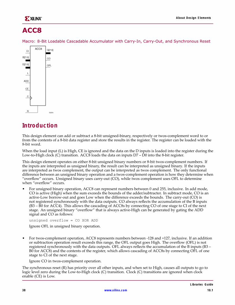
About Design Elements
ACC8Macro: 8-Bit Loadable Cascadable Accumulator with Carry-In, Carry-Out, and Synchronous Reset
IntroductionThis design element can add or subtract a 8-bit unsigned-binary, respectively or twos-complement word to orfrom the contents of a 8-bit data register and store the results in the register. The register can be loaded with the8-bit word.
When the load input (L) is High, CE is ignored and the data on the D inputs is loaded into the register during theLow-to-High clock (C) transition. ACC8 loads the data on inputs D7 – D0 into the 8-bit register.
This design element operates on either 8-bit unsigned binary numbers or 8-bit twos-complement numbers. Ifthe inputs are interpreted as unsigned binary, the result can be interpreted as unsigned binary. If the inputsare interpreted as twos complement, the output can be interpreted as twos complement. The only functionaldifference between an unsigned binary operation and a twos-complement operation is how they determine when“overflow” occurs. Unsigned binary uses carry-out (CO), while twos complement uses OFL to determinewhen “overflow” occurs.• For unsigned binary operation, ACC8 can represent numbers between 0 and 255, inclusive. In add mode,
CO is active (High) when the sum exceeds the bounds of the adder/subtracter. In subtract mode, CO is anactive-Low borrow-out and goes Low when the difference exceeds the bounds. The carry-out (CO) isnot registered synchronously with the data outputs. CO always reflects the accumulation of the B inputs(B3 – B0 for ACC4). This allows the cascading of ACC8s by connecting CO of one stage to CI of the nextstage. An unsigned binary “overflow” that is always active-High can be generated by gating the ADDsignal and CO as follows:unsigned overflow = CO XOR ADD
Ignore OFL in unsigned binary operation.
• For twos-complement operation, ACC8 represents numbers between -128 and +127, inclusive. If an additionor subtraction operation result exceeds this range, the OFL output goes High. The overflow (OFL) is notregistered synchronously with the data outputs. OFL always reflects the accumulation of the B inputs (B3 –B0 for ACC8) and the contents of the register, which allows cascading of ACC8s by connecting OFL of onestage to CI of the next stage.Ignore CO in twos-complement operation.
The synchronous reset (R) has priority over all other inputs, and when set to High, causes all outputs to go tologic level zero during the Low-to-High clock (C) transition. Clock (C) transitions are ignored when clockenable (CE) is Low.
Libraries Guide
38 www.xilinx.com 10.1

About Design Elements
This design element is asynchronously cleared, outputs Low, when power is applied. For FPGA devices,power-on conditions are simulated when global set/reset (GSR) is active. GSR defaults to active-High but can beinverted by adding an inverter in front of the GSR input of the appropriate STARTUP_architecture symbol.
Logic TableInput Output
R L CE ADD D C Q
1 x x x x ↑ 0
0 1 x x Dn ↑ Dn
0 0 1 1 x ↑ Q0+Bn+CI
0 0 1 0 x ↑ Q0-Bn-CI
0 0 0 x x ↑ No Change
Q0: Previous value of Q
Bn: Value of Data input B
CI: Value of input CI
Design Entry MethodThis design element is only for use in schematics.
For More Information• See the Virtex-4 User Guide.
• See the Virtex-4 Data Sheets.
Libraries Guide
10.1 www.xilinx.com 39
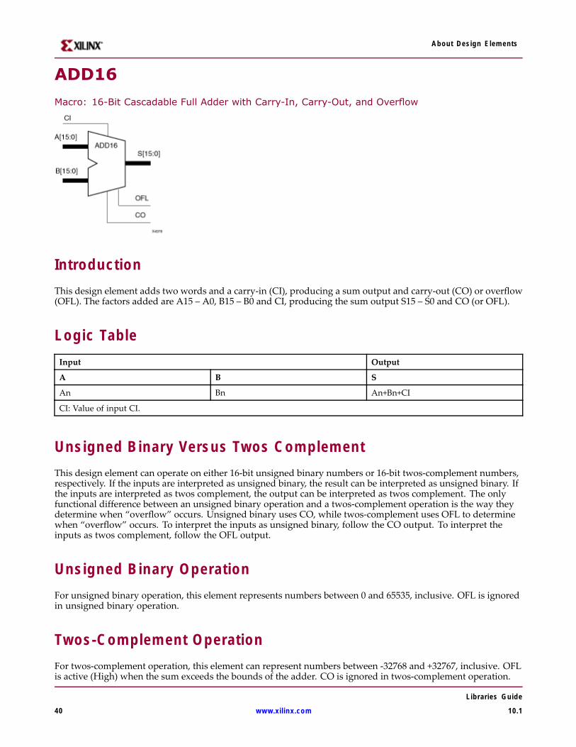
About Design Elements
ADD16
Macro: 16-Bit Cascadable Full Adder with Carry-In, Carry-Out, and Overflow
IntroductionThis design element adds two words and a carry-in (CI), producing a sum output and carry-out (CO) or overflow(OFL). The factors added are A15 – A0, B15 – B0 and CI, producing the sum output S15 – S0 and CO (or OFL).
Logic TableInput Output
A B S
An Bn An+Bn+CI
CI: Value of input CI.
Unsigned Binary Versus Twos ComplementThis design element can operate on either 16-bit unsigned binary numbers or 16-bit twos-complement numbers,respectively. If the inputs are interpreted as unsigned binary, the result can be interpreted as unsigned binary. Ifthe inputs are interpreted as twos complement, the output can be interpreted as twos complement. The onlyfunctional difference between an unsigned binary operation and a twos-complement operation is the way theydetermine when “overflow” occurs. Unsigned binary uses CO, while twos-complement uses OFL to determinewhen “overflow” occurs. To interpret the inputs as unsigned binary, follow the CO output. To interpret theinputs as twos complement, follow the OFL output.
Unsigned Binary OperationFor unsigned binary operation, this element represents numbers between 0 and 65535, inclusive. OFL is ignoredin unsigned binary operation.
Twos-Complement OperationFor twos-complement operation, this element can represent numbers between -32768 and +32767, inclusive. OFLis active (High) when the sum exceeds the bounds of the adder. CO is ignored in twos-complement operation.
Libraries Guide
40 www.xilinx.com 10.1
About Design Elements
Design Entry MethodThis design element is only for use in schematics.
For More Information• See the Virtex-4 User Guide.
• See the Virtex-4 Data Sheets.
Libraries Guide
10.1 www.xilinx.com 41
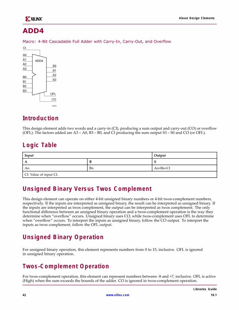
About Design Elements
ADD4Macro: 4-Bit Cascadable Full Adder with Carry-In, Carry-Out, and Overflow
IntroductionThis design element adds two words and a carry-in (CI), producing a sum output and carry-out (CO) or overflow(OFL). The factors added are A3 – A0, B3 – B0, and CI producing the sum output S3 – S0 and CO (or OFL).
Logic TableInput Output
A B S
An Bn An+Bn+CI
CI: Value of input CI.
Unsigned Binary Versus Twos ComplementThis design element can operate on either 4-bit unsigned binary numbers or 4-bit twos-complement numbers,respectively. If the inputs are interpreted as unsigned binary, the result can be interpreted as unsigned binary. Ifthe inputs are interpreted as twos complement, the output can be interpreted as twos complement. The onlyfunctional difference between an unsigned binary operation and a twos-complement operation is the way theydetermine when “overflow” occurs. Unsigned binary uses CO, while twos-complement uses OFL to determinewhen “overflow” occurs. To interpret the inputs as unsigned binary, follow the CO output. To interpret theinputs as twos complement, follow the OFL output.
Unsigned Binary Operation
For unsigned binary operation, this element represents numbers from 0 to 15, inclusive. OFL is ignoredin unsigned binary operation.
Twos-Complement OperationFor twos-complement operation, this element can represent numbers between -8 and +7, inclusive. OFL is active(High) when the sum exceeds the bounds of the adder. CO is ignored in twos-complement operation.
Libraries Guide
42 www.xilinx.com 10.1

About Design Elements
Design Entry MethodThis design element is only for use in schematics.
For More Information• See the Virtex-4 User Guide.
• See the Virtex-4 Data Sheets.
Libraries Guide
10.1 www.xilinx.com 43
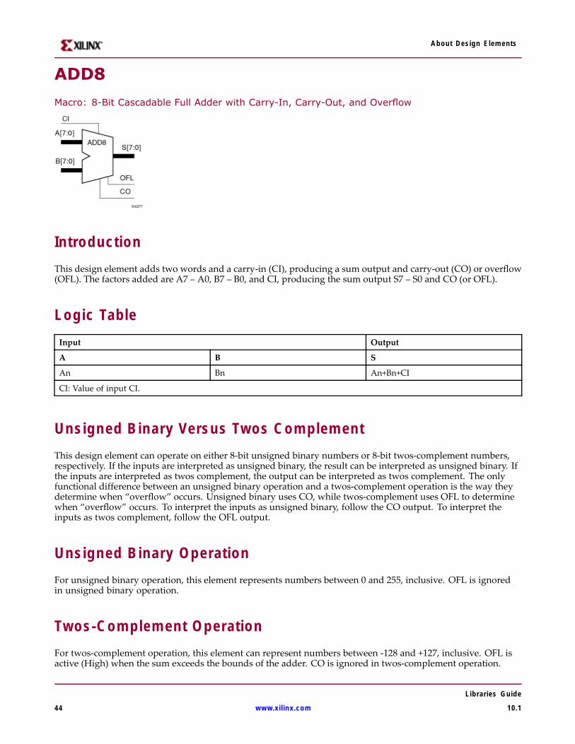
About Design Elements
ADD8
Macro: 8-Bit Cascadable Full Adder with Carry-In, Carry-Out, and Overflow
IntroductionThis design element adds two words and a carry-in (CI), producing a sum output and carry-out (CO) or overflow(OFL). The factors added are A7 – A0, B7 – B0, and CI, producing the sum output S7 – S0 and CO (or OFL).
Logic TableInput Output
A B S
An Bn An+Bn+CI
CI: Value of input CI.
Unsigned Binary Versus Twos ComplementThis design element can operate on either 8-bit unsigned binary numbers or 8-bit twos-complement numbers,respectively. If the inputs are interpreted as unsigned binary, the result can be interpreted as unsigned binary. Ifthe inputs are interpreted as twos complement, the output can be interpreted as twos complement. The onlyfunctional difference between an unsigned binary operation and a twos-complement operation is the way theydetermine when “overflow” occurs. Unsigned binary uses CO, while twos-complement uses OFL to determinewhen “overflow” occurs. To interpret the inputs as unsigned binary, follow the CO output. To interpret theinputs as twos complement, follow the OFL output.
Unsigned Binary OperationFor unsigned binary operation, this element represents numbers between 0 and 255, inclusive. OFL is ignoredin unsigned binary operation.
Twos-Complement OperationFor twos-complement operation, this element can represent numbers between -128 and +127, inclusive. OFL isactive (High) when the sum exceeds the bounds of the adder. CO is ignored in twos-complement operation.
Libraries Guide
44 www.xilinx.com 10.1

About Design Elements
Design Entry MethodThis design element is only for use in schematics.
For More Information• See the Virtex-4 User Guide.
• See the Virtex-4 Data Sheets.
Libraries Guide
10.1 www.xilinx.com 45
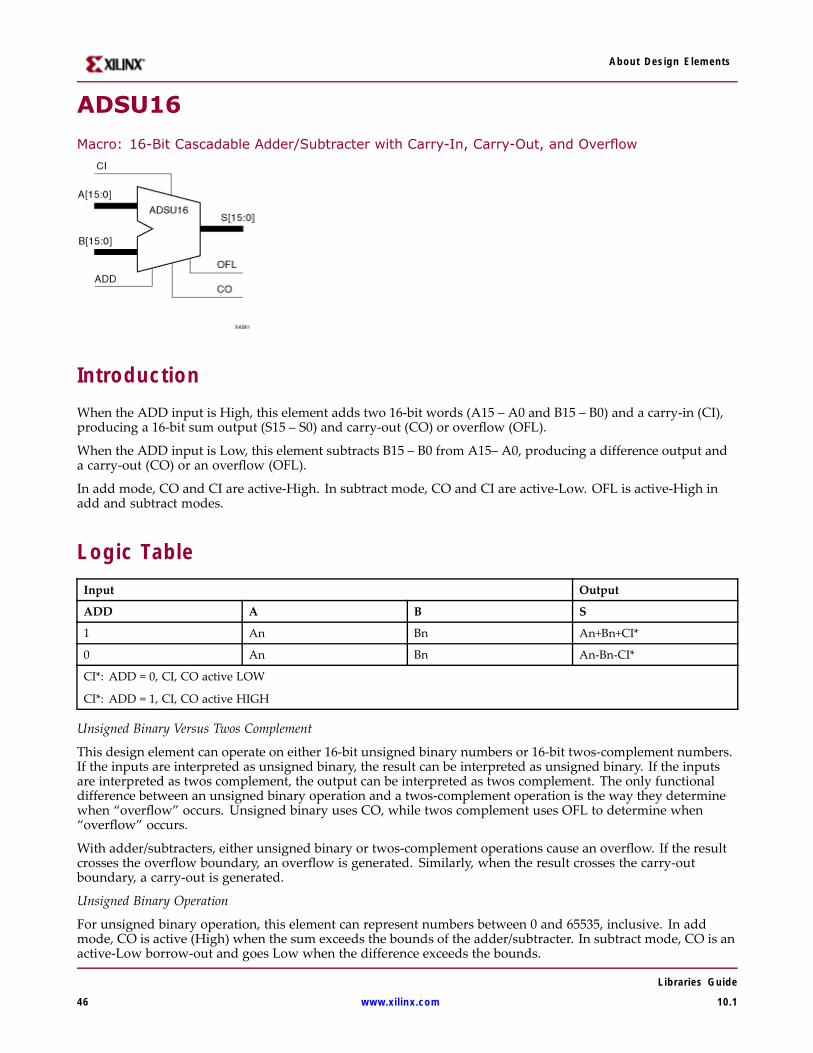
About Design Elements
ADSU16
Macro: 16-Bit Cascadable Adder/Subtracter with Carry-In, Carry-Out, and Overflow
IntroductionWhen the ADD input is High, this element adds two 16-bit words (A15 – A0 and B15 – B0) and a carry-in (CI),producing a 16-bit sum output (S15 – S0) and carry-out (CO) or overflow (OFL).
When the ADD input is Low, this element subtracts B15 – B0 from A15– A0, producing a difference output anda carry-out (CO) or an overflow (OFL).
In add mode, CO and CI are active-High. In subtract mode, CO and CI are active-Low. OFL is active-High inadd and subtract modes.
Logic TableInput Output
ADD A B S
1 An Bn An+Bn+CI*
0 An Bn An-Bn-CI*
CI*: ADD = 0, CI, CO active LOW
CI*: ADD = 1, CI, CO active HIGH
Unsigned Binary Versus Twos Complement
This design element can operate on either 16-bit unsigned binary numbers or 16-bit twos-complement numbers.If the inputs are interpreted as unsigned binary, the result can be interpreted as unsigned binary. If the inputsare interpreted as twos complement, the output can be interpreted as twos complement. The only functionaldifference between an unsigned binary operation and a twos-complement operation is the way they determinewhen “overflow” occurs. Unsigned binary uses CO, while twos complement uses OFL to determine when“overflow” occurs.
With adder/subtracters, either unsigned binary or twos-complement operations cause an overflow. If the resultcrosses the overflow boundary, an overflow is generated. Similarly, when the result crosses the carry-outboundary, a carry-out is generated.
Unsigned Binary Operation
For unsigned binary operation, this element can represent numbers between 0 and 65535, inclusive. In addmode, CO is active (High) when the sum exceeds the bounds of the adder/subtracter. In subtract mode, CO is anactive-Low borrow-out and goes Low when the difference exceeds the bounds.
Libraries Guide
46 www.xilinx.com 10.1
About Design Elements
An unsigned binary “overflow” that is always active-High can be generated by gating the ADD signal and COas follows:unsigned overflow = CO XOR ADD
OFL is ignored in unsigned binary operation.
Twos-Complement Operation
For twos-complement operation, this element can represent numbers between -32768 and +32767, inclusive.
If an addition or subtraction operation result exceeds this range, the OFL output goes High. CO is ignoredin twos-complement operation.
Design Entry MethodThis design element is only for use in schematics.
For More Information• See the Virtex-4 User Guide.
• See the Virtex-4 Data Sheets.
Libraries Guide
10.1 www.xilinx.com 47
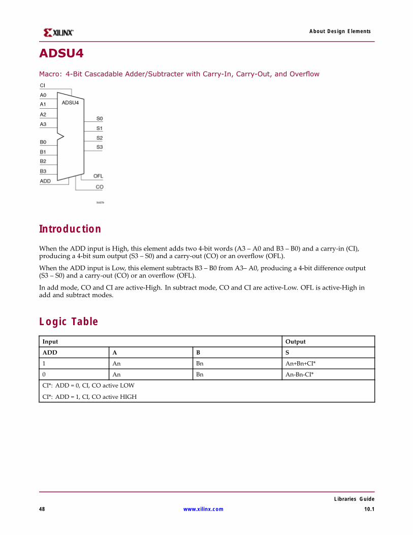
About Design Elements
ADSU4
Macro: 4-Bit Cascadable Adder/Subtracter with Carry-In, Carry-Out, and Overflow
IntroductionWhen the ADD input is High, this element adds two 4-bit words (A3 – A0 and B3 – B0) and a carry-in (CI),producing a 4-bit sum output (S3 – S0) and a carry-out (CO) or an overflow (OFL).
When the ADD input is Low, this element subtracts B3 – B0 from A3– A0, producing a 4-bit difference output(S3 – S0) and a carry-out (CO) or an overflow (OFL).
In add mode, CO and CI are active-High. In subtract mode, CO and CI are active-Low. OFL is active-High inadd and subtract modes.
Logic TableInput Output
ADD A B S
1 An Bn An+Bn+CI*
0 An Bn An-Bn-CI*
CI*: ADD = 0, CI, CO active LOW
CI*: ADD = 1, CI, CO active HIGH
Libraries Guide
48 www.xilinx.com 10.1
About Design Elements
Unsigned Binary Versus Twos Complement
This design element can operate on either 4-bit unsigned binary numbers or 4-bit twos-complement numbers. Ifthe inputs are interpreted as unsigned binary, the result can be interpreted as unsigned binary. If the inputsare interpreted as twos complement, the output can be interpreted as twos complement. The only functionaldifference between an unsigned binary operation and a twos-complement operation is the way they determinewhen “overflow” occurs. Unsigned binary uses CO, while twos complement uses OFL to determine when“overflow” occurs.
With adder/subtracters, either unsigned binary or twos-complement operations cause an overflow. If the resultcrosses the overflow boundary, an overflow is generated. Similarly, when the result crosses the carry-outboundary, a carry-out is generated.
Unsigned Binary Operation
For unsigned binary operation, ADSU4 can represent numbers between 0 and 15, inclusive. In add mode, CO isactive (High) when the sum exceeds the bounds of the adder/subtracter. In subtract mode, CO is an active-Lowborrow-out and goes Low when the difference exceeds the bounds.
An unsigned binary “overflow” that is always active-High can be generated by gating the ADD signal and COas follows:unsigned overflow = CO XOR ADD
OFL is ignored in unsigned binary operation.
Twos-Complement Operation
For twos-complement operation, this element can represent numbers between -8 and +7, inclusive.
If an addition or subtraction operation result exceeds this range, the OFL output goes High. CO is ignoredin twos-complement operation.
Design Entry MethodThis design element is only for use in schematics.
For More Information• See the Virtex-4 User Guide.
• See the Virtex-4 Data Sheets.
Libraries Guide
10.1 www.xilinx.com 49
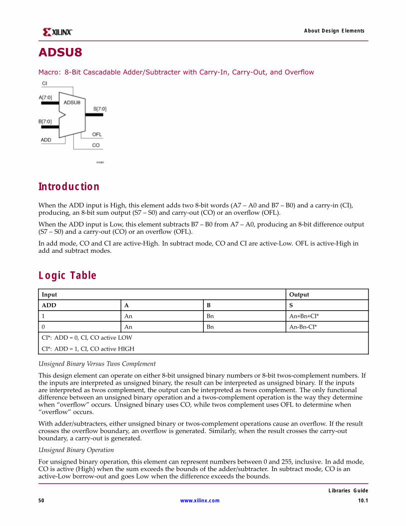
About Design Elements
ADSU8
Macro: 8-Bit Cascadable Adder/Subtracter with Carry-In, Carry-Out, and Overflow
IntroductionWhen the ADD input is High, this element adds two 8-bit words (A7 – A0 and B7 – B0) and a carry-in (CI),producing, an 8-bit sum output (S7 – S0) and carry-out (CO) or an overflow (OFL).
When the ADD input is Low, this element subtracts B7 – B0 from A7 – A0, producing an 8-bit difference output(S7 – S0) and a carry-out (CO) or an overflow (OFL).
In add mode, CO and CI are active-High. In subtract mode, CO and CI are active-Low. OFL is active-High inadd and subtract modes.
Logic TableInput Output
ADD A B S
1 An Bn An+Bn+CI*
0 An Bn An-Bn-CI*
CI*: ADD = 0, CI, CO active LOW
CI*: ADD = 1, CI, CO active HIGH
Unsigned Binary Versus Twos Complement
This design element can operate on either 8-bit unsigned binary numbers or 8-bit twos-complement numbers. Ifthe inputs are interpreted as unsigned binary, the result can be interpreted as unsigned binary. If the inputsare interpreted as twos complement, the output can be interpreted as twos complement. The only functionaldifference between an unsigned binary operation and a twos-complement operation is the way they determinewhen “overflow” occurs. Unsigned binary uses CO, while twos complement uses OFL to determine when“overflow” occurs.
With adder/subtracters, either unsigned binary or twos-complement operations cause an overflow. If the resultcrosses the overflow boundary, an overflow is generated. Similarly, when the result crosses the carry-outboundary, a carry-out is generated.
Unsigned Binary Operation
For unsigned binary operation, this element can represent numbers between 0 and 255, inclusive. In add mode,CO is active (High) when the sum exceeds the bounds of the adder/subtracter. In subtract mode, CO is anactive-Low borrow-out and goes Low when the difference exceeds the bounds.
Libraries Guide
50 www.xilinx.com 10.1
About Design Elements
An unsigned binary “overflow” that is always active-High can be generated by gating the ADD signal and COas follows:unsigned overflow = CO XOR ADD
OFL is ignored in unsigned binary operation.
Twos-Complement Operation
For twos-complement operation, this element can represent numbers between -128 and +127, inclusive.
If an addition or subtraction operation result exceeds this range, the OFL output goes High. CO is ignoredin twos-complement operation.
Design Entry MethodThis design element is only for use in schematics.
For More Information• See the Virtex-4 User Guide.
• See the Virtex-4 Data Sheets.
Libraries Guide
10.1 www.xilinx.com 51

About Design Elements
AND12
Macro: 12- Input AND Gate with Non-Inverted Inputs
IntroductionAND functions of up to five inputs are available in any combination of inverting and non-inverting inputs. ANDfunctions of six to nine inputs, 12 inputs, and 16 inputs are available with noninverting inputs. To make someor all inputs inverting, use external inverters. Because each input uses a CLB resource, replace functions withunused inputs with functions having the appropriate number of inputs.
Design Entry MethodThis design element is only for use in schematics.
For More Information• See the Virtex-4 User Guide.
• See the Virtex-4 Data Sheets.
Libraries Guide
52 www.xilinx.com 10.1
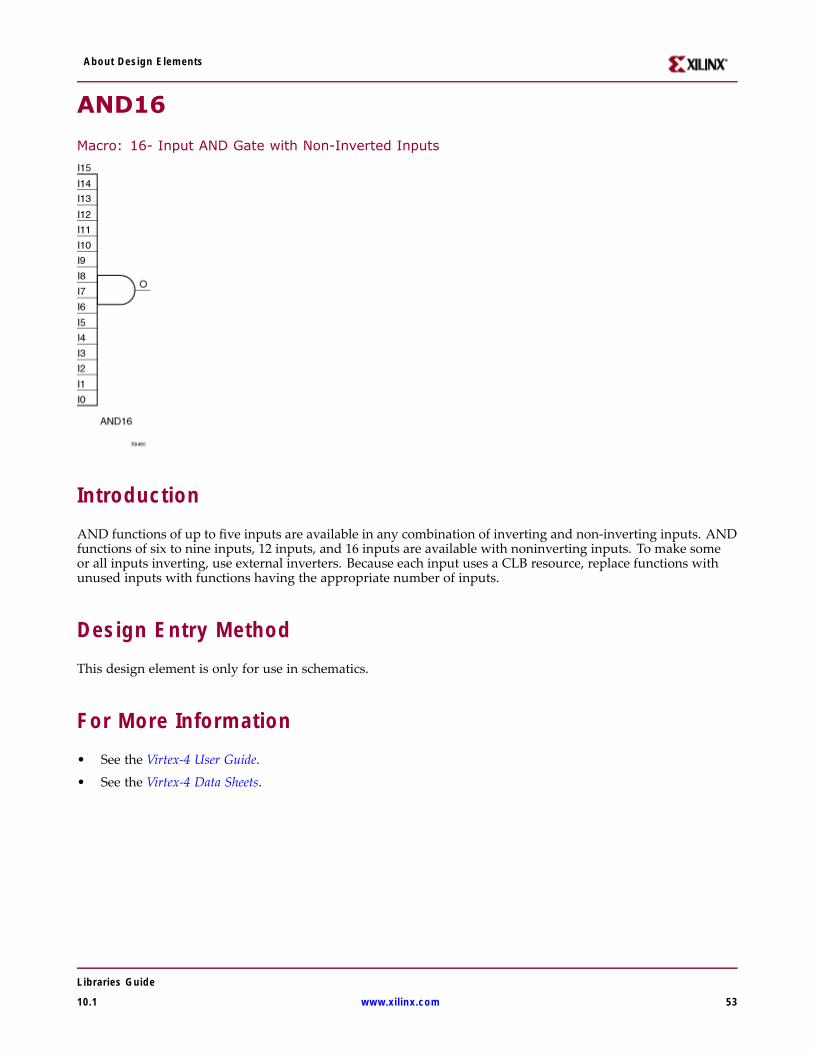
About Design Elements
AND16
Macro: 16- Input AND Gate with Non-Inverted Inputs
IntroductionAND functions of up to five inputs are available in any combination of inverting and non-inverting inputs. ANDfunctions of six to nine inputs, 12 inputs, and 16 inputs are available with noninverting inputs. To make someor all inputs inverting, use external inverters. Because each input uses a CLB resource, replace functions withunused inputs with functions having the appropriate number of inputs.
Design Entry MethodThis design element is only for use in schematics.
For More Information• See the Virtex-4 User Guide.
• See the Virtex-4 Data Sheets.
Libraries Guide
10.1 www.xilinx.com 53
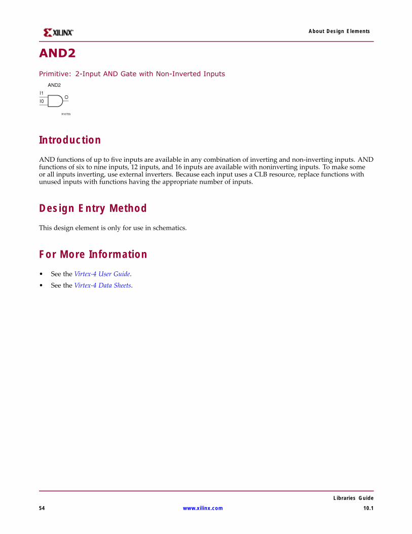
About Design Elements
AND2
Primitive: 2-Input AND Gate with Non-Inverted Inputs
IntroductionAND functions of up to five inputs are available in any combination of inverting and non-inverting inputs. ANDfunctions of six to nine inputs, 12 inputs, and 16 inputs are available with noninverting inputs. To make someor all inputs inverting, use external inverters. Because each input uses a CLB resource, replace functions withunused inputs with functions having the appropriate number of inputs.
Design Entry MethodThis design element is only for use in schematics.
For More Information• See the Virtex-4 User Guide.
• See the Virtex-4 Data Sheets.
Libraries Guide
54 www.xilinx.com 10.1

About Design Elements
AND2B1
Primitive: 2-Input AND Gate with 1 Inverted and 1 Non-Inverted Inputs
IntroductionAND functions of up to five inputs are available in any combination of inverting and non-inverting inputs. ANDfunctions of six to nine inputs, 12 inputs, and 16 inputs are available with noninverting inputs. To make someor all inputs inverting, use external inverters. Because each input uses a CLB resource, replace functions withunused inputs with functions having the appropriate number of inputs.
Design Entry MethodThis design element is only for use in schematics.
For More Information• See the Virtex-4 User Guide.
• See the Virtex-4 Data Sheets.
Libraries Guide
10.1 www.xilinx.com 55
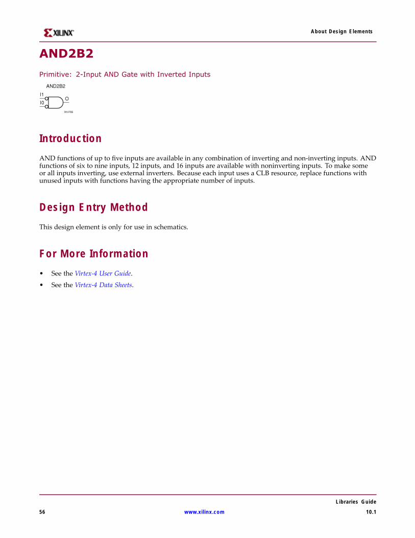
About Design Elements
AND2B2
Primitive: 2-Input AND Gate with Inverted Inputs
IntroductionAND functions of up to five inputs are available in any combination of inverting and non-inverting inputs. ANDfunctions of six to nine inputs, 12 inputs, and 16 inputs are available with noninverting inputs. To make someor all inputs inverting, use external inverters. Because each input uses a CLB resource, replace functions withunused inputs with functions having the appropriate number of inputs.
Design Entry MethodThis design element is only for use in schematics.
For More Information• See the Virtex-4 User Guide.
• See the Virtex-4 Data Sheets.
Libraries Guide
56 www.xilinx.com 10.1
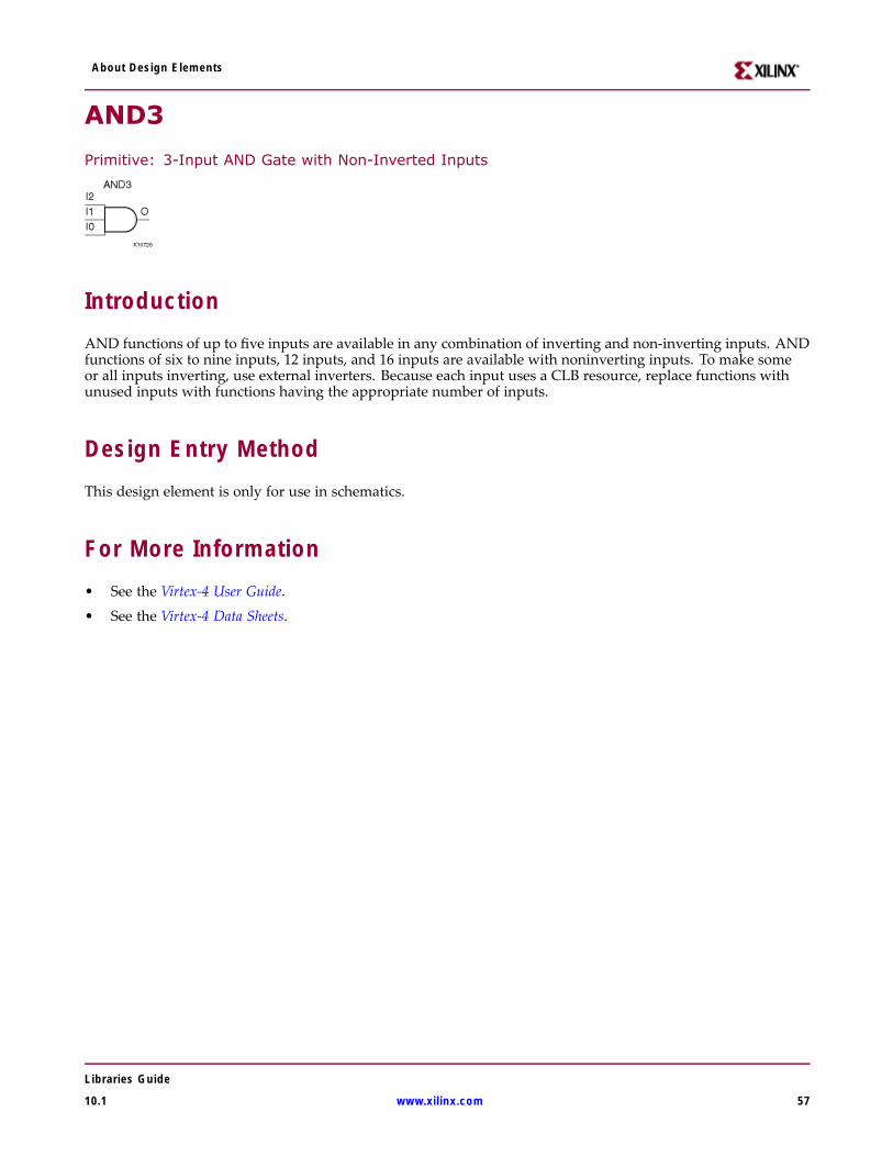
About Design Elements
AND3
Primitive: 3-Input AND Gate with Non-Inverted Inputs
IntroductionAND functions of up to five inputs are available in any combination of inverting and non-inverting inputs. ANDfunctions of six to nine inputs, 12 inputs, and 16 inputs are available with noninverting inputs. To make someor all inputs inverting, use external inverters. Because each input uses a CLB resource, replace functions withunused inputs with functions having the appropriate number of inputs.
Design Entry MethodThis design element is only for use in schematics.
For More Information• See the Virtex-4 User Guide.
• See the Virtex-4 Data Sheets.
Libraries Guide
10.1 www.xilinx.com 57
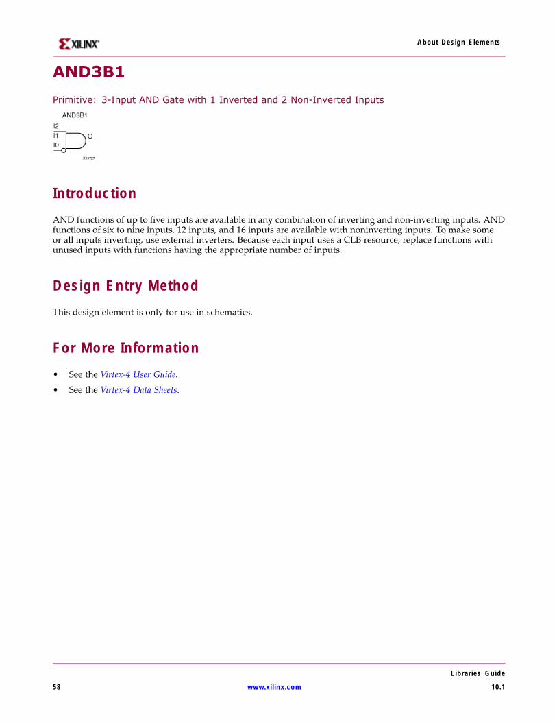
About Design Elements
AND3B1
Primitive: 3-Input AND Gate with 1 Inverted and 2 Non-Inverted Inputs
IntroductionAND functions of up to five inputs are available in any combination of inverting and non-inverting inputs. ANDfunctions of six to nine inputs, 12 inputs, and 16 inputs are available with noninverting inputs. To make someor all inputs inverting, use external inverters. Because each input uses a CLB resource, replace functions withunused inputs with functions having the appropriate number of inputs.
Design Entry MethodThis design element is only for use in schematics.
For More Information• See the Virtex-4 User Guide.
• See the Virtex-4 Data Sheets.
Libraries Guide
58 www.xilinx.com 10.1
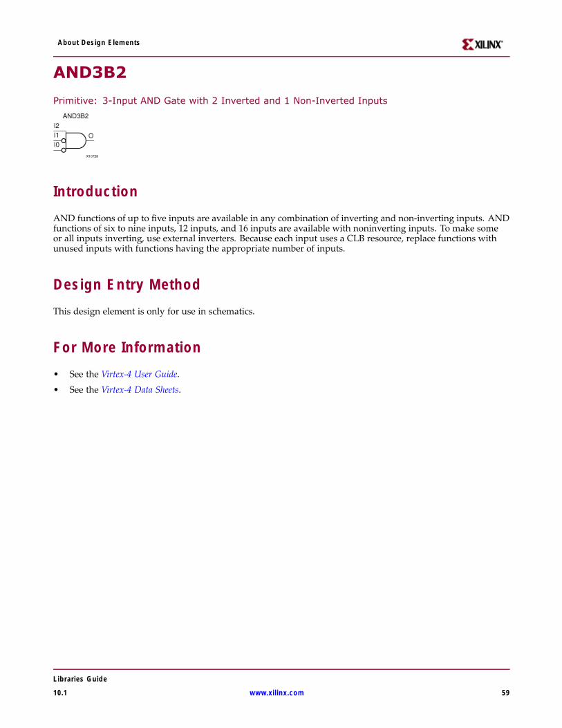
About Design Elements
AND3B2
Primitive: 3-Input AND Gate with 2 Inverted and 1 Non-Inverted Inputs
IntroductionAND functions of up to five inputs are available in any combination of inverting and non-inverting inputs. ANDfunctions of six to nine inputs, 12 inputs, and 16 inputs are available with noninverting inputs. To make someor all inputs inverting, use external inverters. Because each input uses a CLB resource, replace functions withunused inputs with functions having the appropriate number of inputs.
Design Entry MethodThis design element is only for use in schematics.
For More Information• See the Virtex-4 User Guide.
• See the Virtex-4 Data Sheets.
Libraries Guide
10.1 www.xilinx.com 59

About Design Elements
AND3B3
Primitive: 3-Input AND Gate with Inverted Inputs
IntroductionAND functions of up to five inputs are available in any combination of inverting and non-inverting inputs. ANDfunctions of six to nine inputs, 12 inputs, and 16 inputs are available with noninverting inputs. To make someor all inputs inverting, use external inverters. Because each input uses a CLB resource, replace functions withunused inputs with functions having the appropriate number of inputs.
Design Entry MethodThis design element is only for use in schematics.
For More Information• See the Virtex-4 User Guide.
• See the Virtex-4 Data Sheets.
Libraries Guide
60 www.xilinx.com 10.1

About Design Elements
AND4
Primitive: 4-Input AND Gate with Non-Inverted Inputs
IntroductionAND functions of up to five inputs are available in any combination of inverting and non-inverting inputs. ANDfunctions of six to nine inputs, 12 inputs, and 16 inputs are available with noninverting inputs. To make someor all inputs inverting, use external inverters. Because each input uses a CLB resource, replace functions withunused inputs with functions having the appropriate number of inputs.
Design Entry MethodThis design element is only for use in schematics.
For More Information• See the Virtex-4 User Guide.
• See the Virtex-4 Data Sheets.
Libraries Guide
10.1 www.xilinx.com 61

About Design Elements
AND4B1
Primitive: 4-Input AND Gate with 1 Inverted and 3 Non-Inverted Inputs
IntroductionAND functions of up to five inputs are available in any combination of inverting and non-inverting inputs. ANDfunctions of six to nine inputs, 12 inputs, and 16 inputs are available with noninverting inputs. To make someor all inputs inverting, use external inverters. Because each input uses a CLB resource, replace functions withunused inputs with functions having the appropriate number of inputs.
Design Entry MethodThis design element is only for use in schematics.
For More Information• See the Virtex-4 User Guide.
• See the Virtex-4 Data Sheets.
Libraries Guide
62 www.xilinx.com 10.1
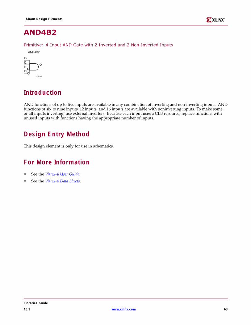
About Design Elements
AND4B2
Primitive: 4-Input AND Gate with 2 Inverted and 2 Non-Inverted Inputs
IntroductionAND functions of up to five inputs are available in any combination of inverting and non-inverting inputs. ANDfunctions of six to nine inputs, 12 inputs, and 16 inputs are available with noninverting inputs. To make someor all inputs inverting, use external inverters. Because each input uses a CLB resource, replace functions withunused inputs with functions having the appropriate number of inputs.
Design Entry MethodThis design element is only for use in schematics.
For More Information• See the Virtex-4 User Guide.
• See the Virtex-4 Data Sheets.
Libraries Guide
10.1 www.xilinx.com 63
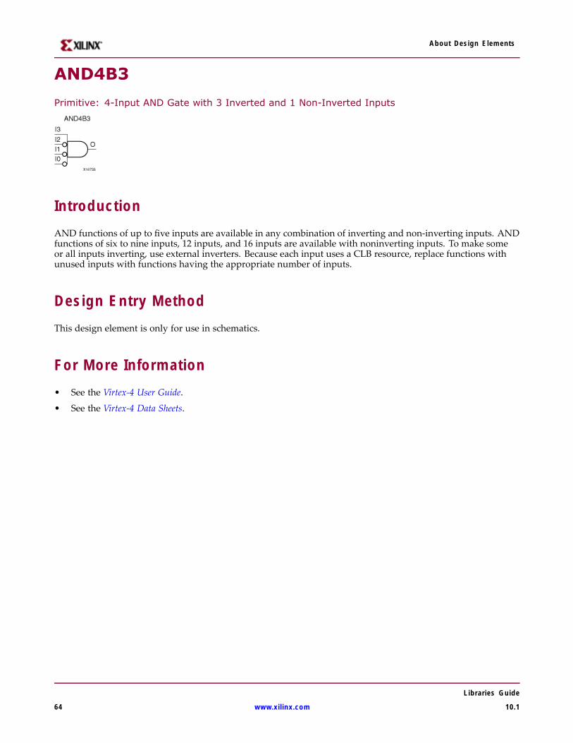
About Design Elements
AND4B3
Primitive: 4-Input AND Gate with 3 Inverted and 1 Non-Inverted Inputs
IntroductionAND functions of up to five inputs are available in any combination of inverting and non-inverting inputs. ANDfunctions of six to nine inputs, 12 inputs, and 16 inputs are available with noninverting inputs. To make someor all inputs inverting, use external inverters. Because each input uses a CLB resource, replace functions withunused inputs with functions having the appropriate number of inputs.
Design Entry MethodThis design element is only for use in schematics.
For More Information• See the Virtex-4 User Guide.
• See the Virtex-4 Data Sheets.
Libraries Guide
64 www.xilinx.com 10.1

About Design Elements
AND4B4
Primitive: 4-Input AND Gate with Inverted Inputs
IntroductionAND functions of up to five inputs are available in any combination of inverting and non-inverting inputs. ANDfunctions of six to nine inputs, 12 inputs, and 16 inputs are available with noninverting inputs. To make someor all inputs inverting, use external inverters. Because each input uses a CLB resource, replace functions withunused inputs with functions having the appropriate number of inputs.
Design Entry MethodThis design element is only for use in schematics.
For More Information• See the Virtex-4 User Guide.
• See the Virtex-4 Data Sheets.
Libraries Guide
10.1 www.xilinx.com 65

About Design Elements
AND5
Primitive: 5-Input AND Gate with Non-Inverted Inputs
IntroductionAND functions of up to five inputs are available in any combination of inverting and non-inverting inputs. ANDfunctions of six to nine inputs, 12 inputs, and 16 inputs are available with noninverting inputs. To make someor all inputs inverting, use external inverters. Because each input uses a CLB resource, replace functions withunused inputs with functions having the appropriate number of inputs.
Design Entry MethodThis design element is only for use in schematics.
For More Information• See the Virtex-4 User Guide.
• See the Virtex-4 Data Sheets.
Libraries Guide
66 www.xilinx.com 10.1

About Design Elements
AND5B1
Primitive: 5-Input AND Gate with 1 Inverted and 4 Non-Inverted Inputs
IntroductionAND functions of up to five inputs are available in any combination of inverting and non-inverting inputs. ANDfunctions of six to nine inputs, 12 inputs, and 16 inputs are available with noninverting inputs. To make someor all inputs inverting, use external inverters. Because each input uses a CLB resource, replace functions withunused inputs with functions having the appropriate number of inputs.
Design Entry MethodThis design element is only for use in schematics.
For More Information• See the Virtex-4 User Guide.
• See the Virtex-4 Data Sheets.
Libraries Guide
10.1 www.xilinx.com 67
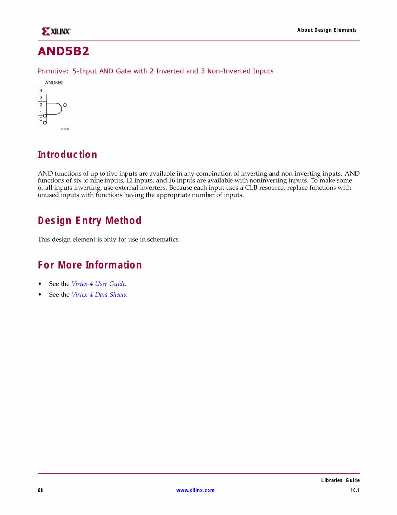
About Design Elements
AND5B2
Primitive: 5-Input AND Gate with 2 Inverted and 3 Non-Inverted Inputs
IntroductionAND functions of up to five inputs are available in any combination of inverting and non-inverting inputs. ANDfunctions of six to nine inputs, 12 inputs, and 16 inputs are available with noninverting inputs. To make someor all inputs inverting, use external inverters. Because each input uses a CLB resource, replace functions withunused inputs with functions having the appropriate number of inputs.
Design Entry MethodThis design element is only for use in schematics.
For More Information• See the Virtex-4 User Guide.
• See the Virtex-4 Data Sheets.
Libraries Guide
68 www.xilinx.com 10.1
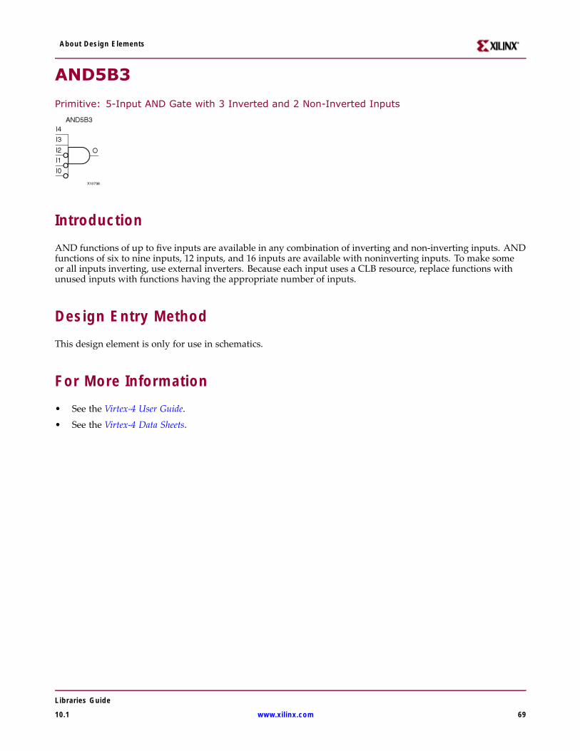
About Design Elements
AND5B3
Primitive: 5-Input AND Gate with 3 Inverted and 2 Non-Inverted Inputs
IntroductionAND functions of up to five inputs are available in any combination of inverting and non-inverting inputs. ANDfunctions of six to nine inputs, 12 inputs, and 16 inputs are available with noninverting inputs. To make someor all inputs inverting, use external inverters. Because each input uses a CLB resource, replace functions withunused inputs with functions having the appropriate number of inputs.
Design Entry MethodThis design element is only for use in schematics.
For More Information• See the Virtex-4 User Guide.
• See the Virtex-4 Data Sheets.
Libraries Guide
10.1 www.xilinx.com 69

About Design Elements
AND5B4
Primitive: 5-Input AND Gate with 4 Inverted and 1 Non-Inverted Inputs
IntroductionAND functions of up to five inputs are available in any combination of inverting and non-inverting inputs. ANDfunctions of six to nine inputs, 12 inputs, and 16 inputs are available with noninverting inputs. To make someor all inputs inverting, use external inverters. Because each input uses a CLB resource, replace functions withunused inputs with functions having the appropriate number of inputs.
Design Entry MethodThis design element is only for use in schematics.
For More Information• See the Virtex-4 User Guide.
• See the Virtex-4 Data Sheets.
Libraries Guide
70 www.xilinx.com 10.1

About Design Elements
AND5B5
Primitive: 5-Input AND Gate with Inverted Inputs
IntroductionAND functions of up to five inputs are available in any combination of inverting and non-inverting inputs. ANDfunctions of six to nine inputs, 12 inputs, and 16 inputs are available with noninverting inputs. To make someor all inputs inverting, use external inverters. Because each input uses a CLB resource, replace functions withunused inputs with functions having the appropriate number of inputs.
Design Entry MethodThis design element is only for use in schematics.
For More Information• See the Virtex-4 User Guide.
• See the Virtex-4 Data Sheets.
Libraries Guide
10.1 www.xilinx.com 71
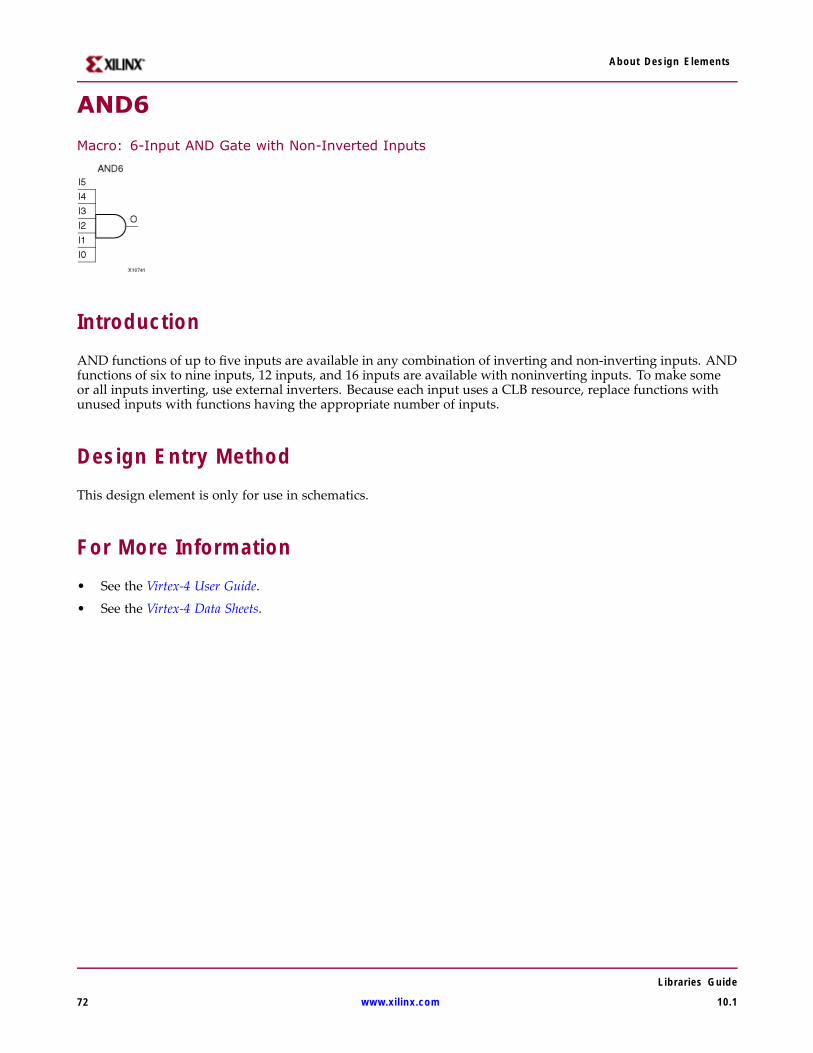
About Design Elements
AND6
Macro: 6-Input AND Gate with Non-Inverted Inputs
IntroductionAND functions of up to five inputs are available in any combination of inverting and non-inverting inputs. ANDfunctions of six to nine inputs, 12 inputs, and 16 inputs are available with noninverting inputs. To make someor all inputs inverting, use external inverters. Because each input uses a CLB resource, replace functions withunused inputs with functions having the appropriate number of inputs.
Design Entry MethodThis design element is only for use in schematics.
For More Information• See the Virtex-4 User Guide.
• See the Virtex-4 Data Sheets.
Libraries Guide
72 www.xilinx.com 10.1
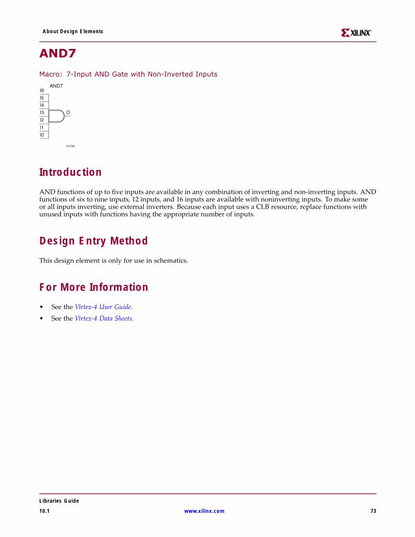
About Design Elements
AND7
Macro: 7-Input AND Gate with Non-Inverted Inputs
IntroductionAND functions of up to five inputs are available in any combination of inverting and non-inverting inputs. ANDfunctions of six to nine inputs, 12 inputs, and 16 inputs are available with noninverting inputs. To make someor all inputs inverting, use external inverters. Because each input uses a CLB resource, replace functions withunused inputs with functions having the appropriate number of inputs.
Design Entry MethodThis design element is only for use in schematics.
For More Information• See the Virtex-4 User Guide.
• See the Virtex-4 Data Sheets.
Libraries Guide
10.1 www.xilinx.com 73
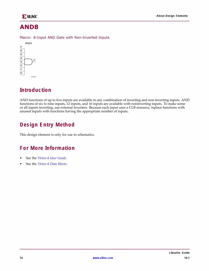
About Design Elements
AND8
Macro: 8-Input AND Gate with Non-Inverted Inputs
IntroductionAND functions of up to five inputs are available in any combination of inverting and non-inverting inputs. ANDfunctions of six to nine inputs, 12 inputs, and 16 inputs are available with noninverting inputs. To make someor all inputs inverting, use external inverters. Because each input uses a CLB resource, replace functions withunused inputs with functions having the appropriate number of inputs.
Design Entry MethodThis design element is only for use in schematics.
For More Information• See the Virtex-4 User Guide.
• See the Virtex-4 Data Sheets.
Libraries Guide
74 www.xilinx.com 10.1
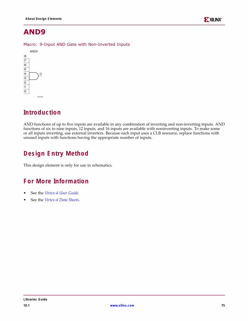
About Design Elements
AND9
Macro: 9-Input AND Gate with Non-Inverted Inputs
IntroductionAND functions of up to five inputs are available in any combination of inverting and non-inverting inputs. ANDfunctions of six to nine inputs, 12 inputs, and 16 inputs are available with noninverting inputs. To make someor all inputs inverting, use external inverters. Because each input uses a CLB resource, replace functions withunused inputs with functions having the appropriate number of inputs.
Design Entry MethodThis design element is only for use in schematics.
For More Information• See the Virtex-4 User Guide.
• See the Virtex-4 Data Sheets.
Libraries Guide
10.1 www.xilinx.com 75
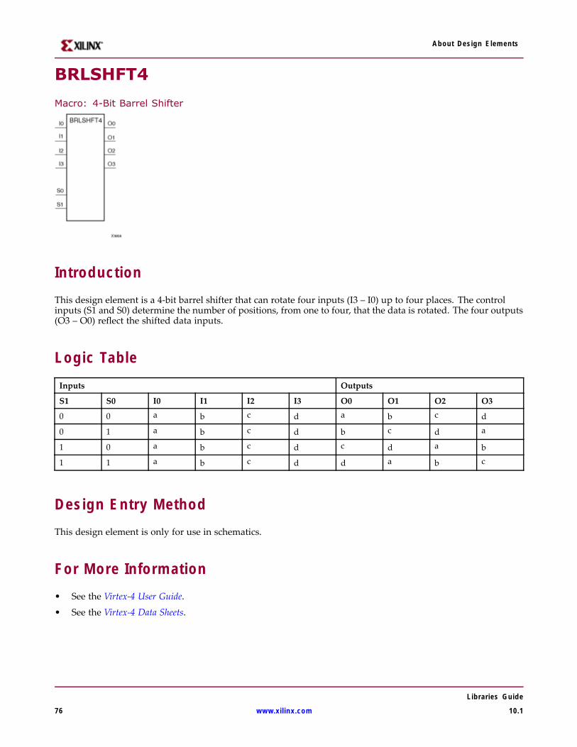
About Design Elements
BRLSHFT4
Macro: 4-Bit Barrel Shifter
IntroductionThis design element is a 4-bit barrel shifter that can rotate four inputs (I3 – I0) up to four places. The controlinputs (S1 and S0) determine the number of positions, from one to four, that the data is rotated. The four outputs(O3 – O0) reflect the shifted data inputs.
Logic TableInputs Outputs
S1 S0 I0 I1 I2 I3 O0 O1 O2 O3
0 0 a b c d a b c d
0 1 a b c d b c d a
1 0 a b c d c d a b
1 1 a b c d d a b c
Design Entry MethodThis design element is only for use in schematics.
For More Information• See the Virtex-4 User Guide.
• See the Virtex-4 Data Sheets.
Libraries Guide
76 www.xilinx.com 10.1
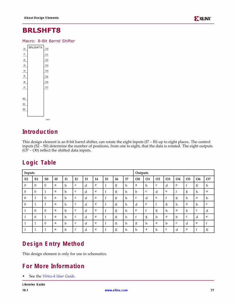
About Design Elements
BRLSHFT8Macro: 8-Bit Barrel Shifter
IntroductionThis design element is an 8-bit barrel shifter, can rotate the eight inputs (I7 – I0) up to eight places. The controlinputs (S2 – S0) determine the number of positions, from one to eight, that the data is rotated. The eight outputs(O7 – O0) reflect the shifted data inputs.
Logic TableInputs Outputs
S2 S1 S0 I0 I1 I2 I3 I4 I5 I6 I7 O0 O1 O2 O3 O4 O5 O6 O7
0 0 0 a b c d e f g h a b c d e f g h
0 0 1 a b c d e f g h b c d e f g h a
0 1 0 a b c d e f g h c d e f g h a b
0 1 1 a b c d e f g h d e f g h a b c
1 0 0 a b c d e f g h e f g h a b c d
1 0 1 a b c d e f g h f g h a b c d e
1 1 0 a b c d e f g h g h a b c d e f
1 1 1 a b c d e f g h h a b c d e f g
Design Entry MethodThis design element is only for use in schematics.
For More Information• See the Virtex-4 User Guide.
Libraries Guide
10.1 www.xilinx.com 77

About Design Elements
• See the Virtex-4 Data Sheets.
Libraries Guide
78 www.xilinx.com 10.1
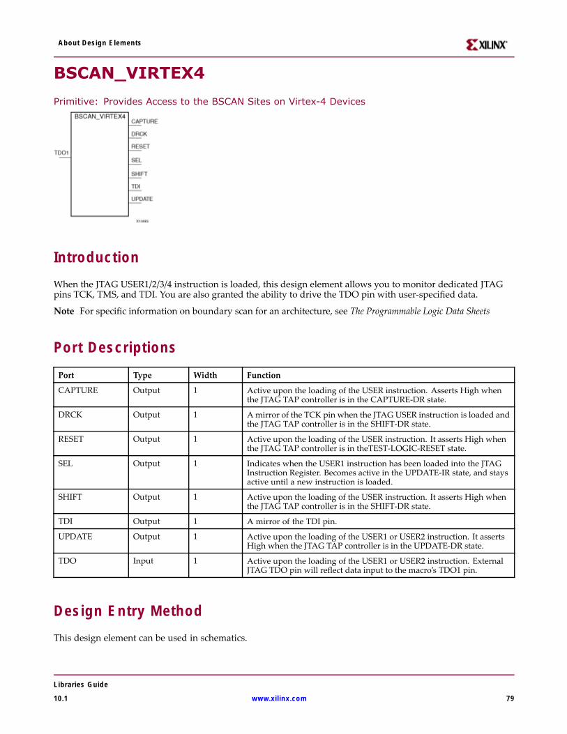
About Design Elements
BSCAN_VIRTEX4
Primitive: Provides Access to the BSCAN Sites on Virtex-4 Devices
IntroductionWhen the JTAG USER1/2/3/4 instruction is loaded, this design element allows you to monitor dedicated JTAGpins TCK, TMS, and TDI. You are also granted the ability to drive the TDO pin with user-specified data.
Note For specific information on boundary scan for an architecture, see The Programmable Logic Data Sheets
Port DescriptionsPort Type Width Function
CAPTURE Output 1 Active upon the loading of the USER instruction. Asserts High whenthe JTAG TAP controller is in the CAPTURE-DR state.
DRCK Output 1 A mirror of the TCK pin when the JTAG USER instruction is loaded andthe JTAG TAP controller is in the SHIFT-DR state.
RESET Output 1 Active upon the loading of the USER instruction. It asserts High whenthe JTAG TAP controller is in theTEST-LOGIC-RESET state.
SEL Output 1 Indicates when the USER1 instruction has been loaded into the JTAGInstruction Register. Becomes active in the UPDATE-IR state, and staysactive until a new instruction is loaded.
SHIFT Output 1 Active upon the loading of the USER instruction. It asserts High whenthe JTAG TAP controller is in the SHIFT-DR state.
TDI Output 1 A mirror of the TDI pin.
UPDATE Output 1 Active upon the loading of the USER1 or USER2 instruction. It assertsHigh when the JTAG TAP controller is in the UPDATE-DR state.
TDO Input 1 Active upon the loading of the USER1 or USER2 instruction. ExternalJTAG TDO pin will reflect data input to the macro’s TDO1 pin.
Design Entry MethodThis design element can be used in schematics.
Libraries Guide
10.1 www.xilinx.com 79

About Design Elements
Available AttributesAttribute Type Allowed Values Default Description
JTAG_CHAIN Integer 1, 2, 3, or 4 1 Used to set the BSCAN site in the device.
For More Information• See the Virtex-4 User Guide.
• See the Virtex-4 Data Sheets.
Libraries Guide
80 www.xilinx.com 10.1
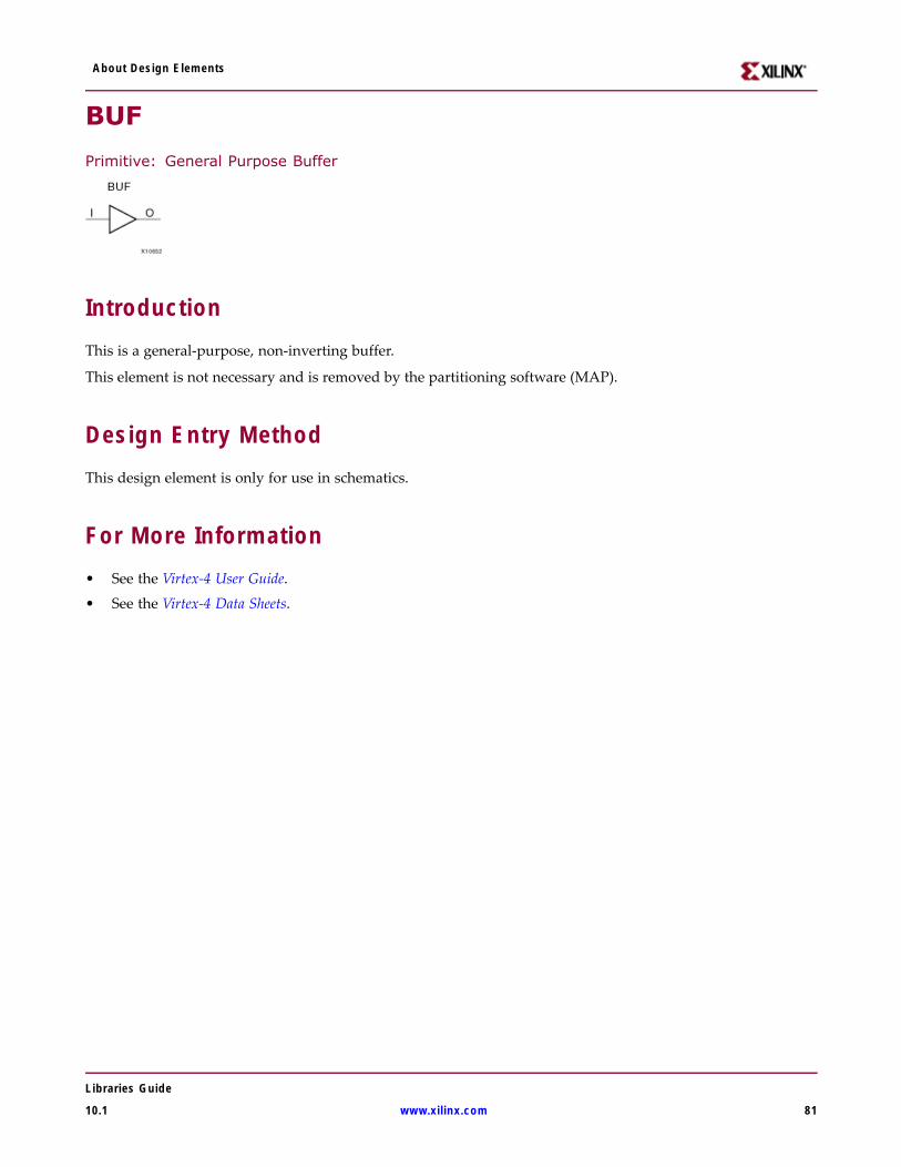
About Design Elements
BUF
Primitive: General Purpose Buffer
IntroductionThis is a general-purpose, non-inverting buffer.
This element is not necessary and is removed by the partitioning software (MAP).
Design Entry MethodThis design element is only for use in schematics.
For More Information• See the Virtex-4 User Guide.
• See the Virtex-4 Data Sheets.
Libraries Guide
10.1 www.xilinx.com 81
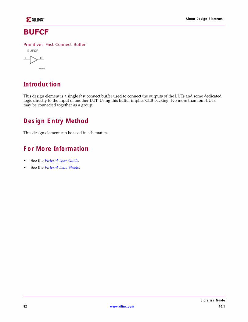
About Design Elements
BUFCF
Primitive: Fast Connect Buffer
IntroductionThis design element is a single fast connect buffer used to connect the outputs of the LUTs and some dedicatedlogic directly to the input of another LUT. Using this buffer implies CLB packing. No more than four LUTsmay be connected together as a group.
Design Entry MethodThis design element can be used in schematics.
For More Information• See the Virtex-4 User Guide.
• See the Virtex-4 Data Sheets.
Libraries Guide
82 www.xilinx.com 10.1
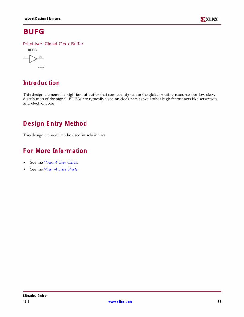
About Design Elements
BUFG
Primitive: Global Clock Buffer
IntroductionThis design element is a high-fanout buffer that connects signals to the global routing resources for low skewdistribution of the signal. BUFGs are typically used on clock nets as well other high fanout nets like sets/resetsand clock enables.
Design Entry MethodThis design element can be used in schematics.
For More Information• See the Virtex-4 User Guide.
• See the Virtex-4 Data Sheets.
Libraries Guide
10.1 www.xilinx.com 83
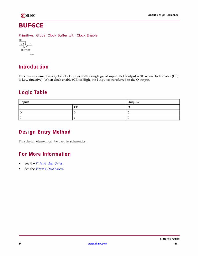
About Design Elements
BUFGCE
Primitive: Global Clock Buffer with Clock Enable
IntroductionThis design element is a global clock buffer with a single gated input. Its O output is "0" when clock enable (CE)is Low (inactive). When clock enable (CE) is High, the I input is transferred to the O output.
Logic TableInputs Outputs
I CE O
X 0 0
I 1 I
Design Entry MethodThis design element can be used in schematics.
For More Information• See the Virtex-4 User Guide.
• See the Virtex-4 Data Sheets.
Libraries Guide
84 www.xilinx.com 10.1
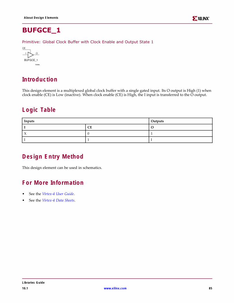
About Design Elements
BUFGCE_1
Primitive: Global Clock Buffer with Clock Enable and Output State 1
IntroductionThis design element is a multiplexed global clock buffer with a single gated input. Its O output is High (1) whenclock enable (CE) is Low (inactive). When clock enable (CE) is High, the I input is transferred to the O output.
Logic TableInputs Outputs
I CE O
X 0 1
I 1 I
Design Entry MethodThis design element can be used in schematics.
For More Information• See the Virtex-4 User Guide.
• See the Virtex-4 Data Sheets.
Libraries Guide
10.1 www.xilinx.com 85
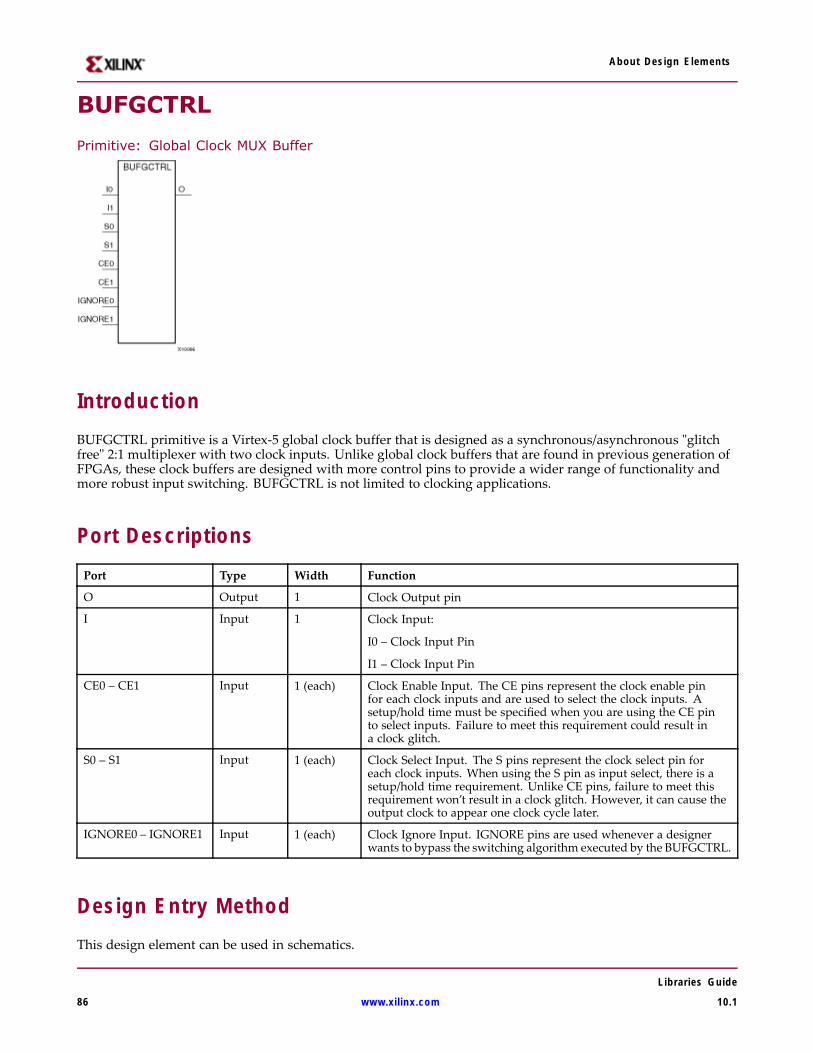
About Design Elements
BUFGCTRL
Primitive: Global Clock MUX Buffer
IntroductionBUFGCTRL primitive is a Virtex-5 global clock buffer that is designed as a synchronous/asynchronous "glitchfree" 2:1 multiplexer with two clock inputs. Unlike global clock buffers that are found in previous generation ofFPGAs, these clock buffers are designed with more control pins to provide a wider range of functionality andmore robust input switching. BUFGCTRL is not limited to clocking applications.
Port DescriptionsPort Type Width Function
O Output 1 Clock Output pin
I Input 1 Clock Input:
I0 – Clock Input Pin
I1 – Clock Input Pin
CE0 – CE1 Input 1 (each) Clock Enable Input. The CE pins represent the clock enable pinfor each clock inputs and are used to select the clock inputs. Asetup/hold time must be specified when you are using the CE pinto select inputs. Failure to meet this requirement could result ina clock glitch.
S0 – S1 Input 1 (each) Clock Select Input. The S pins represent the clock select pin foreach clock inputs. When using the S pin as input select, there is asetup/hold time requirement. Unlike CE pins, failure to meet thisrequirement won’t result in a clock glitch. However, it can cause theoutput clock to appear one clock cycle later.
IGNORE0 – IGNORE1 Input 1 (each) Clock Ignore Input. IGNORE pins are used whenever a designerwants to bypass the switching algorithm executed by the BUFGCTRL.
Design Entry MethodThis design element can be used in schematics.
Libraries Guide
86 www.xilinx.com 10.1
About Design Elements
Available AttributesAttribute Type Allowed Values Default Description
INIT_OUT Integer 0 or 1 0 Initializes the BUFGCTRL output to the specifiedvalue after configuration.
PRESELECT_I0 Boolean FALSE, TRUE FALSE If TRUE, BUFGCTRL output uses I0 input afterconfiguration.
PRESELECT_I1 Boolean FALSE, TRUE FALSE If TRUE, BUFGCTRL output uses I1 input afterconfiguration.
Note Both PRESELECT attributes might not be TRUE at the same time.
For More Information• See the Virtex-4 User Guide.
• See the Virtex-4 Data Sheets.
Libraries Guide
10.1 www.xilinx.com 87
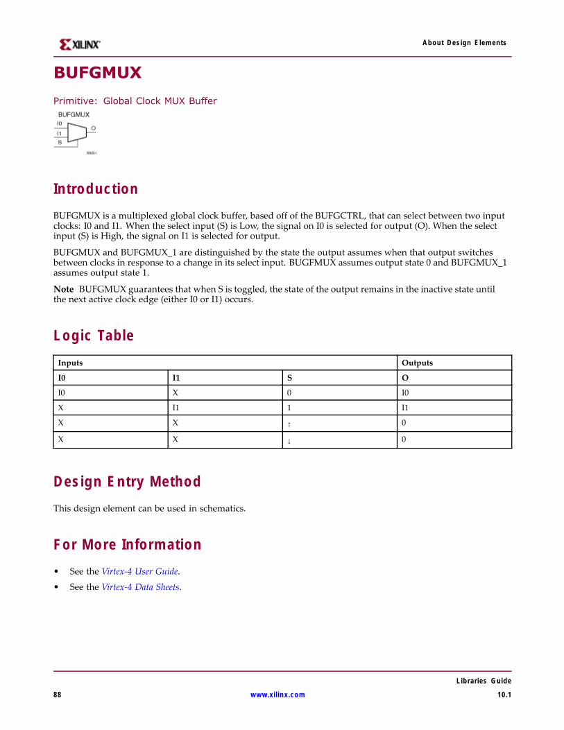
About Design Elements
BUFGMUX
Primitive: Global Clock MUX Buffer
IntroductionBUFGMUX is a multiplexed global clock buffer, based off of the BUFGCTRL, that can select between two inputclocks: I0 and I1. When the select input (S) is Low, the signal on I0 is selected for output (O). When the selectinput (S) is High, the signal on I1 is selected for output.
BUFGMUX and BUFGMUX_1 are distinguished by the state the output assumes when that output switchesbetween clocks in response to a change in its select input. BUGFMUX assumes output state 0 and BUFGMUX_1assumes output state 1.
Note BUFGMUX guarantees that when S is toggled, the state of the output remains in the inactive state untilthe next active clock edge (either I0 or I1) occurs.
Logic TableInputs Outputs
I0 I1 S O
I0 X 0 I0
X I1 1 I1
X X ↑ 0
X X ↓ 0
Design Entry MethodThis design element can be used in schematics.
For More Information• See the Virtex-4 User Guide.
• See the Virtex-4 Data Sheets.
Libraries Guide
88 www.xilinx.com 10.1
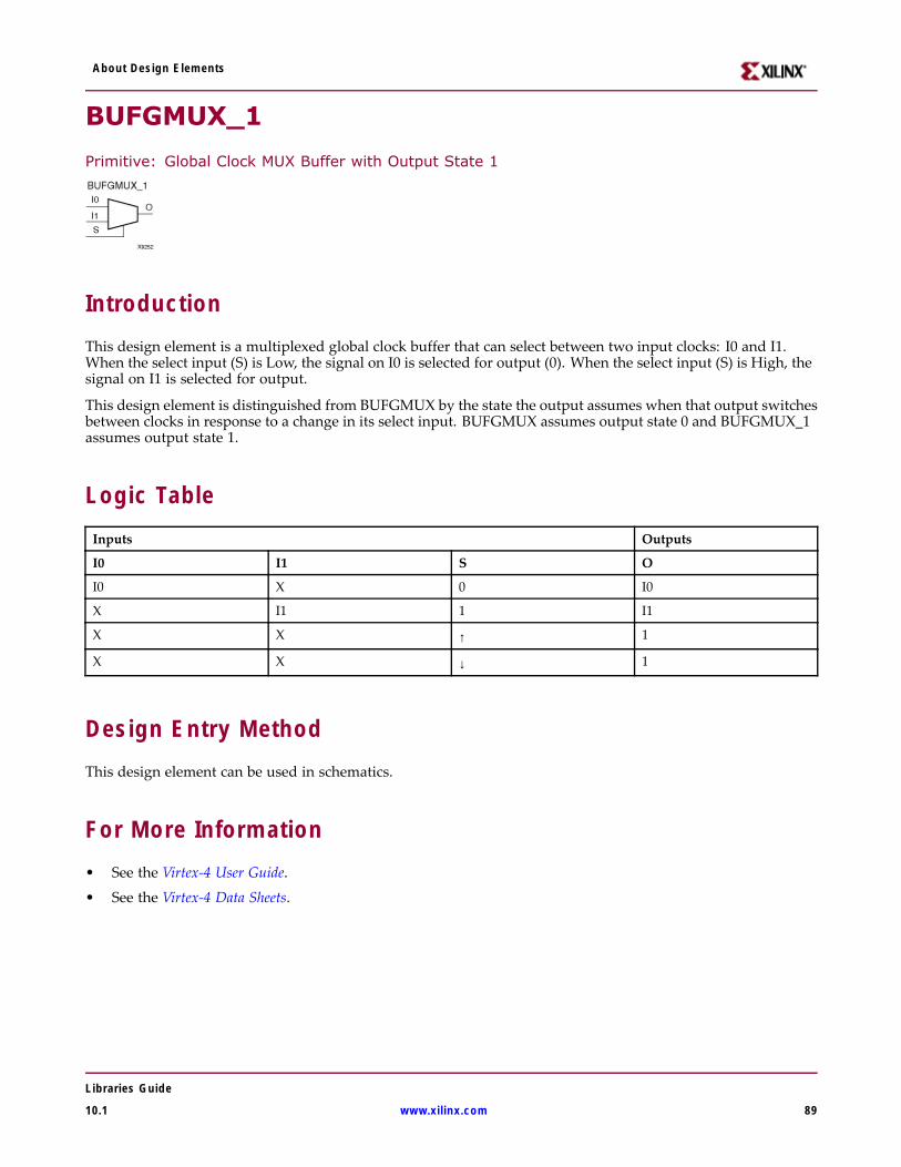
About Design Elements
BUFGMUX_1
Primitive: Global Clock MUX Buffer with Output State 1
IntroductionThis design element is a multiplexed global clock buffer that can select between two input clocks: I0 and I1.When the select input (S) is Low, the signal on I0 is selected for output (0). When the select input (S) is High, thesignal on I1 is selected for output.
This design element is distinguished from BUFGMUX by the state the output assumes when that output switchesbetween clocks in response to a change in its select input. BUFGMUX assumes output state 0 and BUFGMUX_1assumes output state 1.
Logic TableInputs Outputs
I0 I1 S O
I0 X 0 I0
X I1 1 I1
X X ↑ 1
X X ↓ 1
Design Entry MethodThis design element can be used in schematics.
For More Information• See the Virtex-4 User Guide.
• See the Virtex-4 Data Sheets.
Libraries Guide
10.1 www.xilinx.com 89
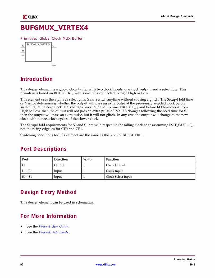
About Design Elements
BUFGMUX_VIRTEX4
Primitive: Global Clock MUX Buffer
IntroductionThis design element is a global clock buffer with two clock inputs, one clock output, and a select line. Thisprimitive is based on BUFGCTRL, with some pins connected to logic High or Low.
This element uses the S pins as select pins. S can switch anytime without causing a glitch. The Setup/Hold timeon S is for determining whether the output will pass an extra pulse of the previously selected clock beforeswitching to the new clock. If S changes prior to the setup time TBCCCK_S, and before I/O transitions fromHigh to Low, then the output will not pass an extra pulse of I/O. If S changes following the hold time for S,then the output will pass an extra pulse, but it will not glitch. In any case the output will change to the newclock within three clock cycles of the slower clock.
The Setup/Hold requirements for S0 and S1 are with respect to the falling clock edge (assuming INIT_OUT = 0),not the rising edge, as for CE0 and CE1.
Switching conditions for this element are the same as the S pin of BUFGCTRL.
Port DescriptionsPort Direction Width Function
O Output 1 Clock Output
I1 - I0 Input 1 Clock Input
S0 – S1 Input 1 Clock Select Input
Design Entry MethodThis design element can be used in schematics.
For More Information• See the Virtex-4 User Guide.
• See the Virtex-4 Data Sheets.
Libraries Guide
90 www.xilinx.com 10.1
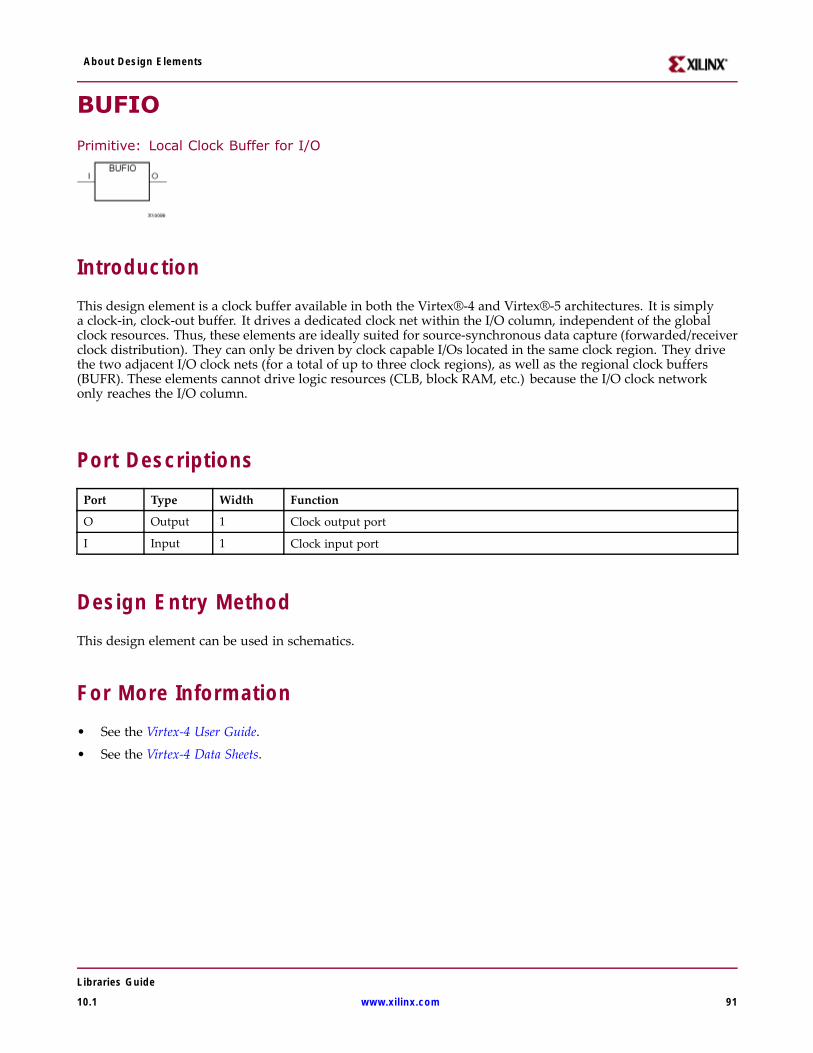
About Design Elements
BUFIO
Primitive: Local Clock Buffer for I/O
IntroductionThis design element is a clock buffer available in both the Virtex®-4 and Virtex®-5 architectures. It is simplya clock-in, clock-out buffer. It drives a dedicated clock net within the I/O column, independent of the globalclock resources. Thus, these elements are ideally suited for source-synchronous data capture (forwarded/receiverclock distribution). They can only be driven by clock capable I/Os located in the same clock region. They drivethe two adjacent I/O clock nets (for a total of up to three clock regions), as well as the regional clock buffers(BUFR). These elements cannot drive logic resources (CLB, block RAM, etc.) because the I/O clock networkonly reaches the I/O column.
Port DescriptionsPort Type Width Function
O Output 1 Clock output port
I Input 1 Clock input port
Design Entry MethodThis design element can be used in schematics.
For More Information• See the Virtex-4 User Guide.
• See the Virtex-4 Data Sheets.
Libraries Guide
10.1 www.xilinx.com 91
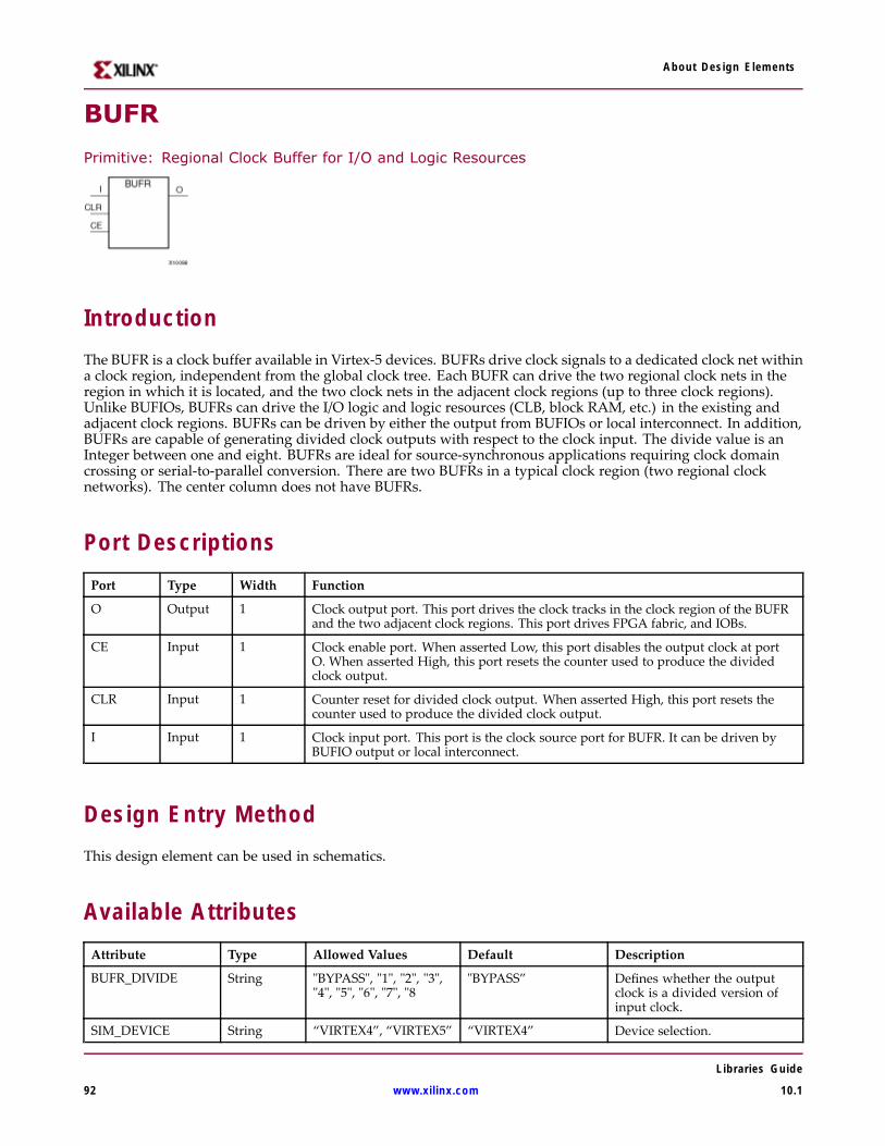
About Design Elements
BUFR
Primitive: Regional Clock Buffer for I/O and Logic Resources
IntroductionThe BUFR is a clock buffer available in Virtex-5 devices. BUFRs drive clock signals to a dedicated clock net withina clock region, independent from the global clock tree. Each BUFR can drive the two regional clock nets in theregion in which it is located, and the two clock nets in the adjacent clock regions (up to three clock regions).Unlike BUFIOs, BUFRs can drive the I/O logic and logic resources (CLB, block RAM, etc.) in the existing andadjacent clock regions. BUFRs can be driven by either the output from BUFIOs or local interconnect. In addition,BUFRs are capable of generating divided clock outputs with respect to the clock input. The divide value is anInteger between one and eight. BUFRs are ideal for source-synchronous applications requiring clock domaincrossing or serial-to-parallel conversion. There are two BUFRs in a typical clock region (two regional clocknetworks). The center column does not have BUFRs.
Port DescriptionsPort Type Width Function
O Output 1 Clock output port. This port drives the clock tracks in the clock region of the BUFRand the two adjacent clock regions. This port drives FPGA fabric, and IOBs.
CE Input 1 Clock enable port. When asserted Low, this port disables the output clock at portO. When asserted High, this port resets the counter used to produce the dividedclock output.
CLR Input 1 Counter reset for divided clock output. When asserted High, this port resets thecounter used to produce the divided clock output.
I Input 1 Clock input port. This port is the clock source port for BUFR. It can be driven byBUFIO output or local interconnect.
Design Entry MethodThis design element can be used in schematics.
Available AttributesAttribute Type Allowed Values Default Description
BUFR_DIVIDE String "BYPASS", "1", "2", "3","4", "5", "6", "7", "8
"BYPASS” Defines whether the outputclock is a divided version ofinput clock.
SIM_DEVICE String “VIRTEX4”, “VIRTEX5” “VIRTEX4” Device selection.
Libraries Guide
92 www.xilinx.com 10.1

About Design Elements
For More Information• See the Virtex-4 User Guide.
• See the Virtex-4 Data Sheets.
Libraries Guide
10.1 www.xilinx.com 93
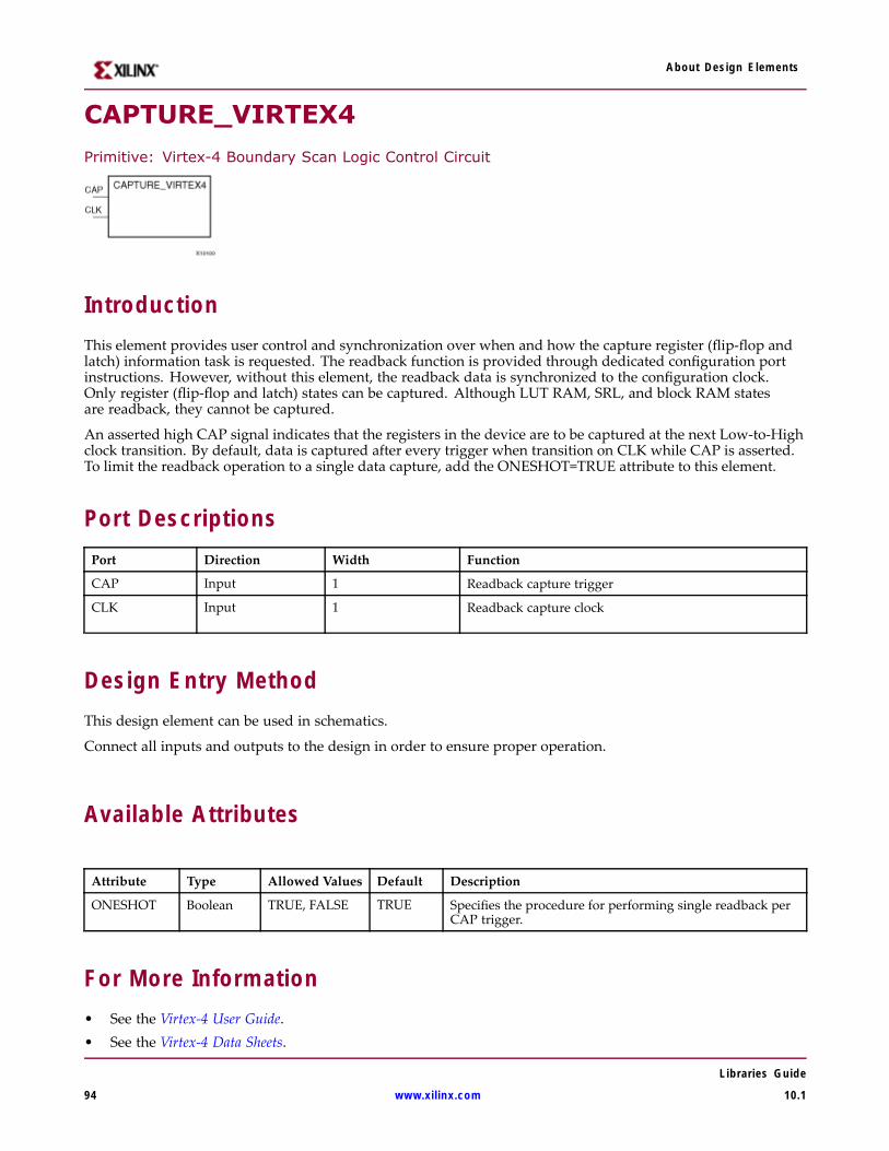
About Design Elements
CAPTURE_VIRTEX4
Primitive: Virtex-4 Boundary Scan Logic Control Circuit
IntroductionThis element provides user control and synchronization over when and how the capture register (flip-flop andlatch) information task is requested. The readback function is provided through dedicated configuration portinstructions. However, without this element, the readback data is synchronized to the configuration clock.Only register (flip-flop and latch) states can be captured. Although LUT RAM, SRL, and block RAM statesare readback, they cannot be captured.
An asserted high CAP signal indicates that the registers in the device are to be captured at the next Low-to-Highclock transition. By default, data is captured after every trigger when transition on CLK while CAP is asserted.To limit the readback operation to a single data capture, add the ONESHOT=TRUE attribute to this element.
Port DescriptionsPort Direction Width Function
CAP Input 1 Readback capture trigger
CLK Input 1 Readback capture clock
Design Entry MethodThis design element can be used in schematics.
Connect all inputs and outputs to the design in order to ensure proper operation.
Available Attributes
Attribute Type Allowed Values Default Description
ONESHOT Boolean TRUE, FALSE TRUE Specifies the procedure for performing single readback perCAP trigger.
For More Information• See the Virtex-4 User Guide.• See the Virtex-4 Data Sheets.
Libraries Guide
94 www.xilinx.com 10.1
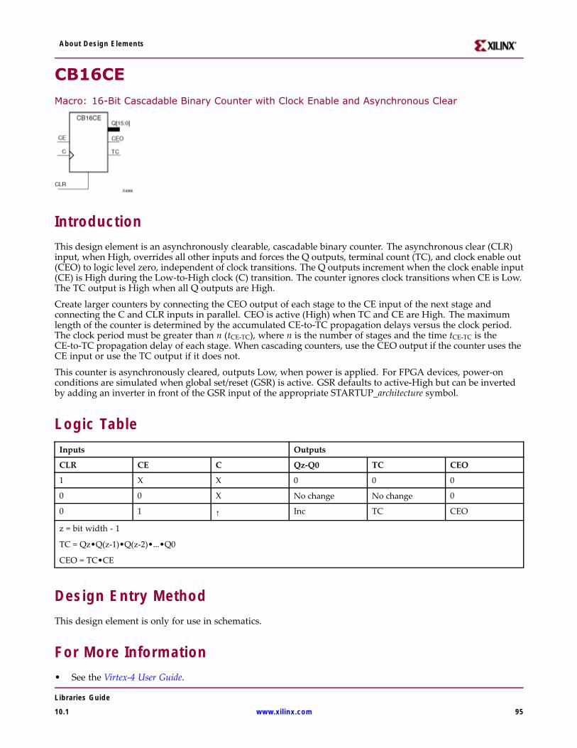
About Design Elements
CB16CEMacro: 16-Bit Cascadable Binary Counter with Clock Enable and Asynchronous Clear
IntroductionThis design element is an asynchronously clearable, cascadable binary counter. The asynchronous clear (CLR)input, when High, overrides all other inputs and forces the Q outputs, terminal count (TC), and clock enable out(CEO) to logic level zero, independent of clock transitions. The Q outputs increment when the clock enable input(CE) is High during the Low-to-High clock (C) transition. The counter ignores clock transitions when CE is Low.The TC output is High when all Q outputs are High.
Create larger counters by connecting the CEO output of each stage to the CE input of the next stage andconnecting the C and CLR inputs in parallel. CEO is active (High) when TC and CE are High. The maximumlength of the counter is determined by the accumulated CE-to-TC propagation delays versus the clock period.The clock period must be greater than n (tCE-TC), where n is the number of stages and the time tCE-TC is theCE-to-TC propagation delay of each stage. When cascading counters, use the CEO output if the counter uses theCE input or use the TC output if it does not.
This counter is asynchronously cleared, outputs Low, when power is applied. For FPGA devices, power-onconditions are simulated when global set/reset (GSR) is active. GSR defaults to active-High but can be invertedby adding an inverter in front of the GSR input of the appropriate STARTUP_architecture symbol.
Logic TableInputs Outputs
CLR CE C Qz-Q0 TC CEO
1 X X 0 0 0
0 0 X No change No change 0
0 1 ↑ Inc TC CEO
z = bit width - 1
TC = Qz•Q(z-1)•Q(z-2)•...•Q0
CEO = TC•CE
Design Entry MethodThis design element is only for use in schematics.
For More Information• See the Virtex-4 User Guide.
Libraries Guide
10.1 www.xilinx.com 95

About Design Elements
• See the Virtex-4 Data Sheets.
Libraries Guide
96 www.xilinx.com 10.1
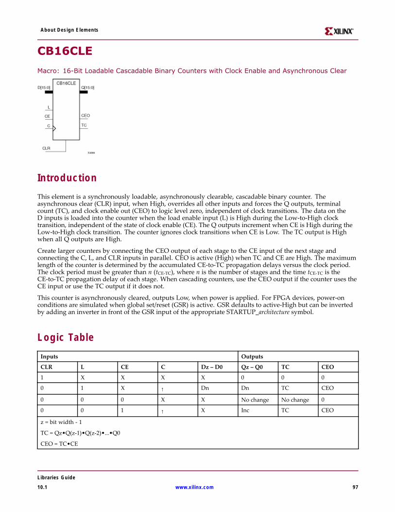
About Design Elements
CB16CLE
Macro: 16-Bit Loadable Cascadable Binary Counters with Clock Enable and Asynchronous Clear
IntroductionThis element is a synchronously loadable, asynchronously clearable, cascadable binary counter. Theasynchronous clear (CLR) input, when High, overrides all other inputs and forces the Q outputs, terminalcount (TC), and clock enable out (CEO) to logic level zero, independent of clock transitions. The data on theD inputs is loaded into the counter when the load enable input (L) is High during the Low-to-High clocktransition, independent of the state of clock enable (CE). The Q outputs increment when CE is High during theLow-to-High clock transition. The counter ignores clock transitions when CE is Low. The TC output is Highwhen all Q outputs are High.
Create larger counters by connecting the CEO output of each stage to the CE input of the next stage andconnecting the C, L, and CLR inputs in parallel. CEO is active (High) when TC and CE are High. The maximumlength of the counter is determined by the accumulated CE-to-TC propagation delays versus the clock period.The clock period must be greater than n (tCE-TC), where n is the number of stages and the time tCE-TC is theCE-to-TC propagation delay of each stage. When cascading counters, use the CEO output if the counter uses theCE input or use the TC output if it does not.
This counter is asynchronously cleared, outputs Low, when power is applied. For FPGA devices, power-onconditions are simulated when global set/reset (GSR) is active. GSR defaults to active-High but can be invertedby adding an inverter in front of the GSR input of the appropriate STARTUP_architecture symbol.
Logic TableInputs Outputs
CLR L CE C Dz – D0 Qz – Q0 TC CEO
1 X X X X 0 0 0
0 1 X ↑ Dn Dn TC CEO
0 0 0 X X No change No change 0
0 0 1 ↑ X Inc TC CEO
z = bit width - 1
TC = Qz•Q(z-1)•Q(z-2)•...•Q0
CEO = TC•CE
Libraries Guide
10.1 www.xilinx.com 97
About Design Elements
Design Entry MethodThis design element is only for use in schematics.
For More Information• See the Virtex-4 User Guide.
• See the Virtex-4 Data Sheets.
Libraries Guide
98 www.xilinx.com 10.1
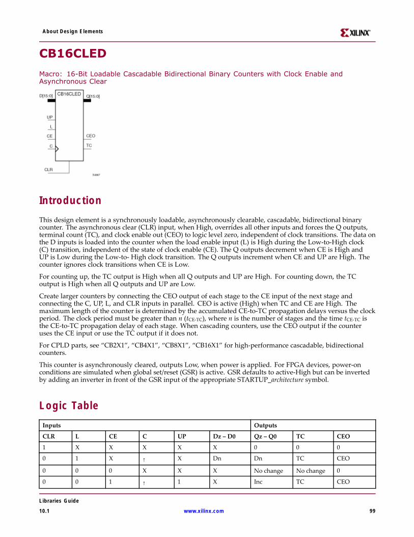
About Design Elements
CB16CLED
Macro: 16-Bit Loadable Cascadable Bidirectional Binary Counters with Clock Enable andAsynchronous Clear
IntroductionThis design element is a synchronously loadable, asynchronously clearable, cascadable, bidirectional binarycounter. The asynchronous clear (CLR) input, when High, overrides all other inputs and forces the Q outputs,terminal count (TC), and clock enable out (CEO) to logic level zero, independent of clock transitions. The data onthe D inputs is loaded into the counter when the load enable input (L) is High during the Low-to-High clock(C) transition, independent of the state of clock enable (CE). The Q outputs decrement when CE is High andUP is Low during the Low-to- High clock transition. The Q outputs increment when CE and UP are High. Thecounter ignores clock transitions when CE is Low.
For counting up, the TC output is High when all Q outputs and UP are High. For counting down, the TCoutput is High when all Q outputs and UP are Low.
Create larger counters by connecting the CEO output of each stage to the CE input of the next stage andconnecting the C, UP, L, and CLR inputs in parallel. CEO is active (High) when TC and CE are High. Themaximum length of the counter is determined by the accumulated CE-to-TC propagation delays versus the clockperiod. The clock period must be greater than n (tCE-TC), where n is the number of stages and the time tCE-TC isthe CE-to-TC propagation delay of each stage. When cascading counters, use the CEO output if the counteruses the CE input or use the TC output if it does not.
For CPLD parts, see “CB2X1”, “CB4X1”, “CB8X1”, “CB16X1” for high-performance cascadable, bidirectionalcounters.
This counter is asynchronously cleared, outputs Low, when power is applied. For FPGA devices, power-onconditions are simulated when global set/reset (GSR) is active. GSR defaults to active-High but can be invertedby adding an inverter in front of the GSR input of the appropriate STARTUP_architecture symbol.
Logic TableInputs Outputs
CLR L CE C UP Dz – D0 Qz – Q0 TC CEO
1 X X X X X 0 0 0
0 1 X ↑ X Dn Dn TC CEO
0 0 0 X X X No change No change 0
0 0 1 ↑ 1 X Inc TC CEO
Libraries Guide
10.1 www.xilinx.com 99

About Design Elements
Inputs Outputs
CLR L CE C UP Dz – D0 Qz – Q0 TC CEO
0 0 1 ↑ 0 X Dec TC CEO
z = bit width - 1
TC = (Qz•Q(z-1)•Q(z-2)•...•Q0•UP) + (Qz•Q(z-1)•Q(z-2)•...•Q0•UP)
CEO = TC•CE
Design Entry MethodThis design element is only for use in schematics.
For More Information• See the Virtex-4 User Guide.
• See the Virtex-4 Data Sheets.
Libraries Guide
100 www.xilinx.com 10.1
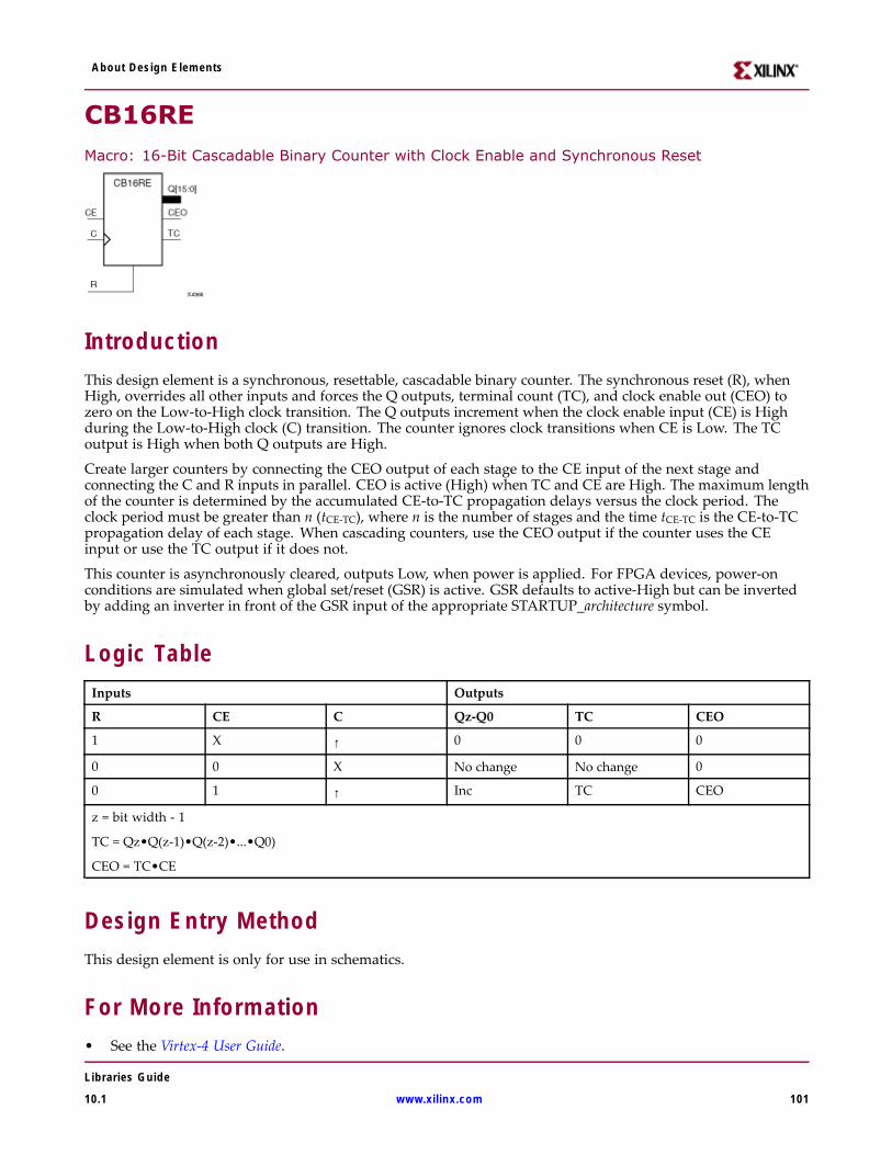
About Design Elements
CB16REMacro: 16-Bit Cascadable Binary Counter with Clock Enable and Synchronous Reset
IntroductionThis design element is a synchronous, resettable, cascadable binary counter. The synchronous reset (R), whenHigh, overrides all other inputs and forces the Q outputs, terminal count (TC), and clock enable out (CEO) tozero on the Low-to-High clock transition. The Q outputs increment when the clock enable input (CE) is Highduring the Low-to-High clock (C) transition. The counter ignores clock transitions when CE is Low. The TCoutput is High when both Q outputs are High.
Create larger counters by connecting the CEO output of each stage to the CE input of the next stage andconnecting the C and R inputs in parallel. CEO is active (High) when TC and CE are High. The maximum lengthof the counter is determined by the accumulated CE-to-TC propagation delays versus the clock period. Theclock period must be greater than n (tCE-TC), where n is the number of stages and the time tCE-TC is the CE-to-TCpropagation delay of each stage. When cascading counters, use the CEO output if the counter uses the CEinput or use the TC output if it does not.
This counter is asynchronously cleared, outputs Low, when power is applied. For FPGA devices, power-onconditions are simulated when global set/reset (GSR) is active. GSR defaults to active-High but can be invertedby adding an inverter in front of the GSR input of the appropriate STARTUP_architecture symbol.
Logic TableInputs Outputs
R CE C Qz-Q0 TC CEO
1 X ↑ 0 0 0
0 0 X No change No change 0
0 1 ↑ Inc TC CEO
z = bit width - 1
TC = Qz•Q(z-1)•Q(z-2)•...•Q0)
CEO = TC•CE
Design Entry MethodThis design element is only for use in schematics.
For More Information• See the Virtex-4 User Guide.
Libraries Guide
10.1 www.xilinx.com 101

About Design Elements
• See the Virtex-4 Data Sheets.
Libraries Guide
102 www.xilinx.com 10.1

About Design Elements
CB2CE
Macro: 2-Bit Cascadable Binary Counter with Clock Enable and Asynchronous Clear
IntroductionThis design element is an asynchronously clearable, cascadable binary counter. The asynchronous clear (CLR)input, when High, overrides all other inputs and forces the Q outputs, terminal count (TC), and clock enable out(CEO) to logic level zero, independent of clock transitions. The Q outputs increment when the clock enable input(CE) is High during the Low-to-High clock (C) transition. The counter ignores clock transitions when CE is Low.The TC output is High when all Q outputs are High.
Create larger counters by connecting the CEO output of each stage to the CE input of the next stage andconnecting the C and CLR inputs in parallel. CEO is active (High) when TC and CE are High. The maximumlength of the counter is determined by the accumulated CE-to-TC propagation delays versus the clock period.The clock period must be greater than n (tCE-TC), where n is the number of stages and the time tCE-TC is theCE-to-TC propagation delay of each stage. When cascading counters, use the CEO output if the counter uses theCE input or use the TC output if it does not.
This counter is asynchronously cleared, outputs Low, when power is applied. For FPGA devices, power-onconditions are simulated when global set/reset (GSR) is active. GSR defaults to active-High but can be invertedby adding an inverter in front of the GSR input of the appropriate STARTUP_architecture symbol.
Logic TableInputs Outputs
CLR CE C Qz-Q0 TC CEO
1 X X 0 0 0
0 0 X No change No change 0
0 1 ↑ Inc TC CEO
z = bit width - 1
TC = Qz•Q(z-1)•Q(z-2)•...•Q0
CEO = TC•CE
Design Entry MethodThis design element is only for use in schematics.
Libraries Guide
10.1 www.xilinx.com 103

About Design Elements
For More Information• See the Virtex-4 User Guide.
• See the Virtex-4 Data Sheets.
Libraries Guide
104 www.xilinx.com 10.1
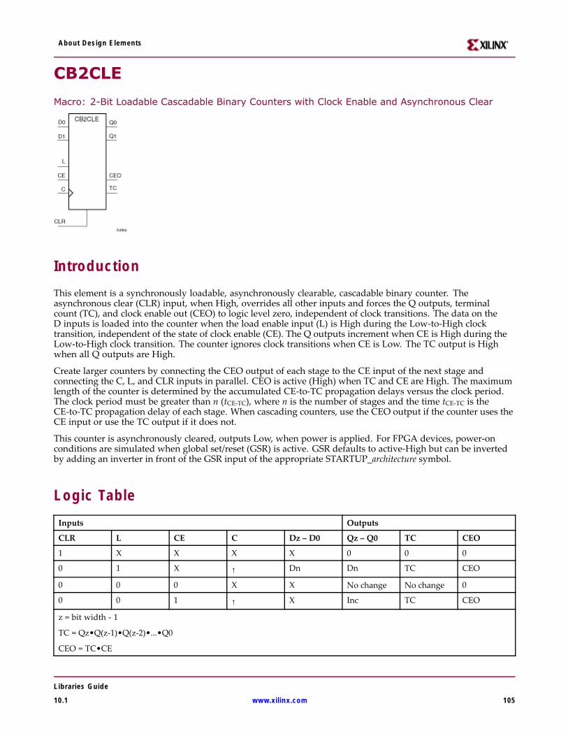
About Design Elements
CB2CLE
Macro: 2-Bit Loadable Cascadable Binary Counters with Clock Enable and Asynchronous Clear
IntroductionThis element is a synchronously loadable, asynchronously clearable, cascadable binary counter. Theasynchronous clear (CLR) input, when High, overrides all other inputs and forces the Q outputs, terminalcount (TC), and clock enable out (CEO) to logic level zero, independent of clock transitions. The data on theD inputs is loaded into the counter when the load enable input (L) is High during the Low-to-High clocktransition, independent of the state of clock enable (CE). The Q outputs increment when CE is High during theLow-to-High clock transition. The counter ignores clock transitions when CE is Low. The TC output is Highwhen all Q outputs are High.
Create larger counters by connecting the CEO output of each stage to the CE input of the next stage andconnecting the C, L, and CLR inputs in parallel. CEO is active (High) when TC and CE are High. The maximumlength of the counter is determined by the accumulated CE-to-TC propagation delays versus the clock period.The clock period must be greater than n (tCE-TC), where n is the number of stages and the time tCE-TC is theCE-to-TC propagation delay of each stage. When cascading counters, use the CEO output if the counter uses theCE input or use the TC output if it does not.
This counter is asynchronously cleared, outputs Low, when power is applied. For FPGA devices, power-onconditions are simulated when global set/reset (GSR) is active. GSR defaults to active-High but can be invertedby adding an inverter in front of the GSR input of the appropriate STARTUP_architecture symbol.
Logic TableInputs Outputs
CLR L CE C Dz – D0 Qz – Q0 TC CEO
1 X X X X 0 0 0
0 1 X ↑ Dn Dn TC CEO
0 0 0 X X No change No change 0
0 0 1 ↑ X Inc TC CEO
z = bit width - 1
TC = Qz•Q(z-1)•Q(z-2)•...•Q0
CEO = TC•CE
Libraries Guide
10.1 www.xilinx.com 105

About Design Elements
Design Entry MethodThis design element is only for use in schematics.
For More Information• See the Virtex-4 User Guide.
• See the Virtex-4 Data Sheets.
Libraries Guide
106 www.xilinx.com 10.1
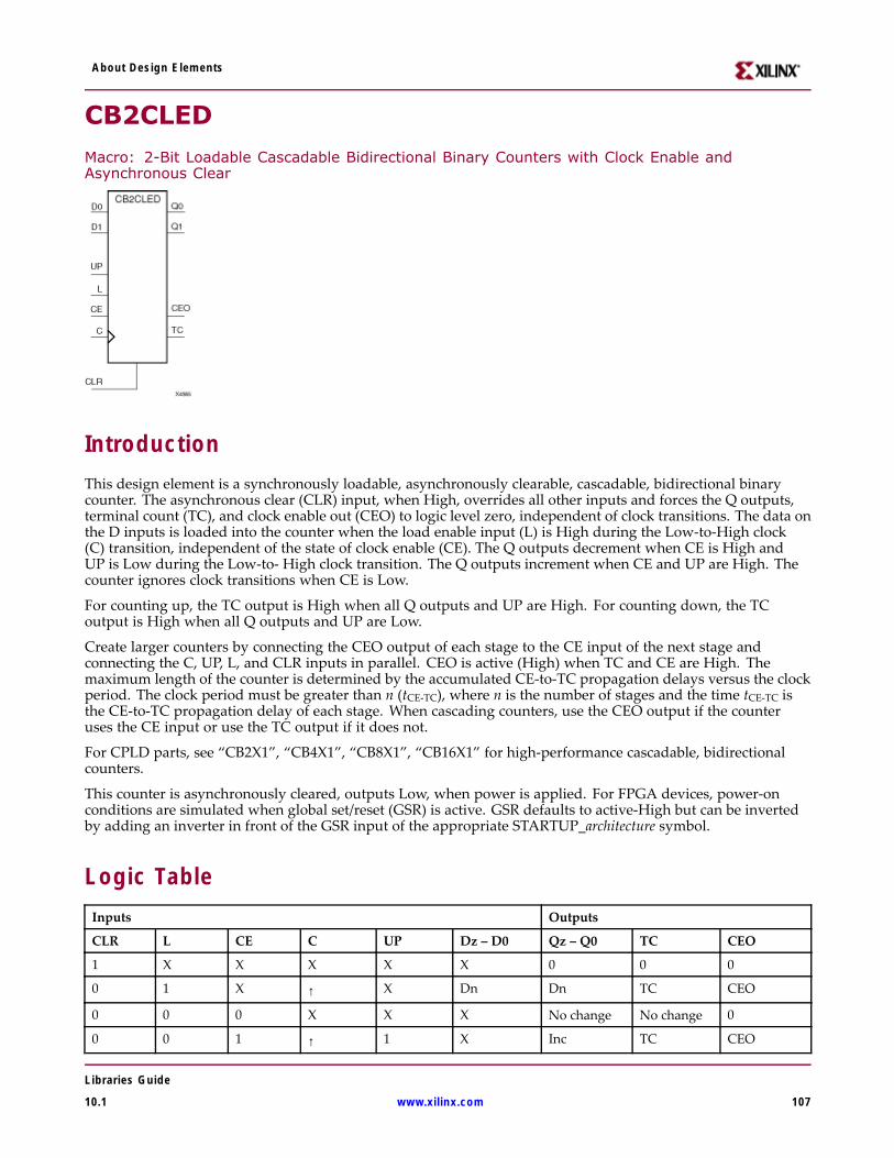
About Design Elements
CB2CLED
Macro: 2-Bit Loadable Cascadable Bidirectional Binary Counters with Clock Enable andAsynchronous Clear
IntroductionThis design element is a synchronously loadable, asynchronously clearable, cascadable, bidirectional binarycounter. The asynchronous clear (CLR) input, when High, overrides all other inputs and forces the Q outputs,terminal count (TC), and clock enable out (CEO) to logic level zero, independent of clock transitions. The data onthe D inputs is loaded into the counter when the load enable input (L) is High during the Low-to-High clock(C) transition, independent of the state of clock enable (CE). The Q outputs decrement when CE is High andUP is Low during the Low-to- High clock transition. The Q outputs increment when CE and UP are High. Thecounter ignores clock transitions when CE is Low.
For counting up, the TC output is High when all Q outputs and UP are High. For counting down, the TCoutput is High when all Q outputs and UP are Low.
Create larger counters by connecting the CEO output of each stage to the CE input of the next stage andconnecting the C, UP, L, and CLR inputs in parallel. CEO is active (High) when TC and CE are High. Themaximum length of the counter is determined by the accumulated CE-to-TC propagation delays versus the clockperiod. The clock period must be greater than n (tCE-TC), where n is the number of stages and the time tCE-TC isthe CE-to-TC propagation delay of each stage. When cascading counters, use the CEO output if the counteruses the CE input or use the TC output if it does not.
For CPLD parts, see “CB2X1”, “CB4X1”, “CB8X1”, “CB16X1” for high-performance cascadable, bidirectionalcounters.
This counter is asynchronously cleared, outputs Low, when power is applied. For FPGA devices, power-onconditions are simulated when global set/reset (GSR) is active. GSR defaults to active-High but can be invertedby adding an inverter in front of the GSR input of the appropriate STARTUP_architecture symbol.
Logic TableInputs Outputs
CLR L CE C UP Dz – D0 Qz – Q0 TC CEO
1 X X X X X 0 0 0
0 1 X ↑ X Dn Dn TC CEO
0 0 0 X X X No change No change 0
0 0 1 ↑ 1 X Inc TC CEO
Libraries Guide
10.1 www.xilinx.com 107

About Design Elements
Inputs Outputs
CLR L CE C UP Dz – D0 Qz – Q0 TC CEO
0 0 1 ↑ 0 X Dec TC CEO
z = bit width - 1
TC = (Qz•Q(z-1)•Q(z-2)•...•Q0•UP) + (Qz•Q(z-1)•Q(z-2)•...•Q0•UP)
CEO = TC•CE
Design Entry MethodThis design element is only for use in schematics.
For More Information• See the Virtex-4 User Guide.
• See the Virtex-4 Data Sheets.
Libraries Guide
108 www.xilinx.com 10.1
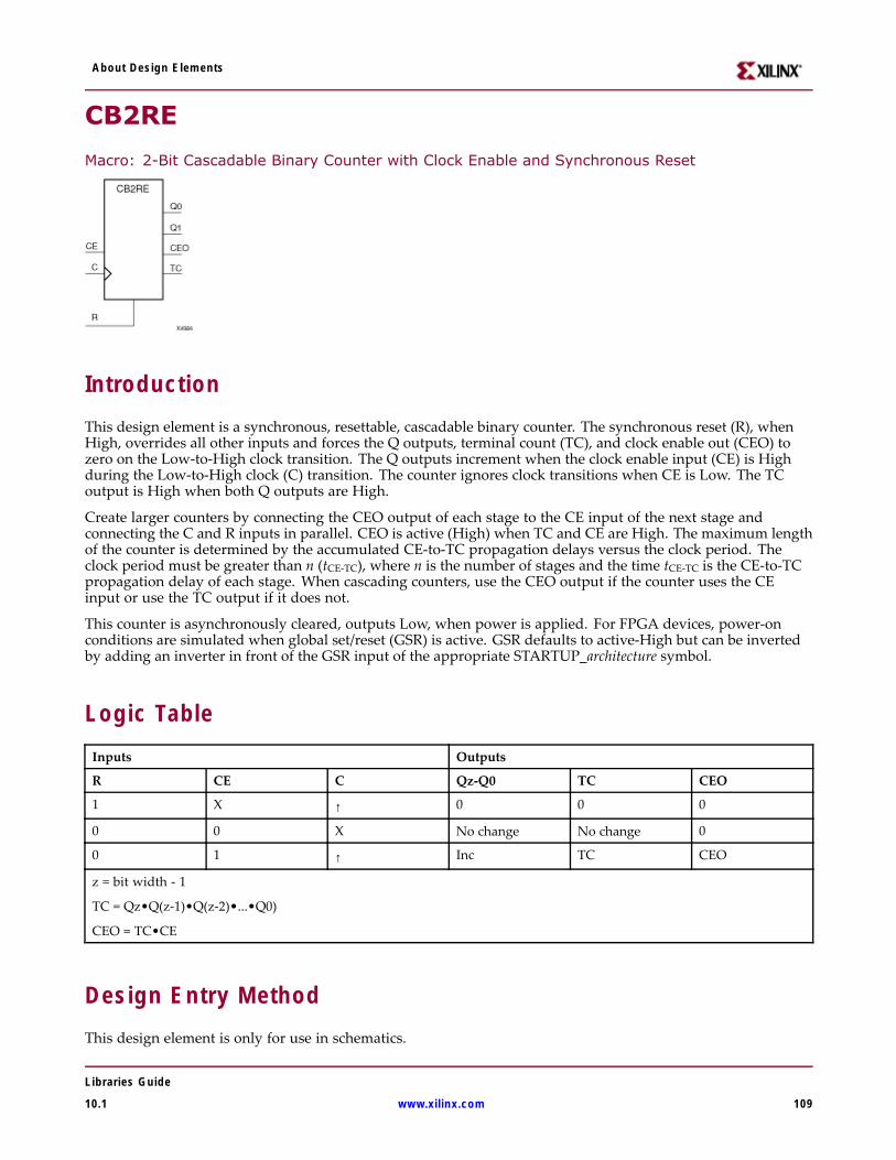
About Design Elements
CB2RE
Macro: 2-Bit Cascadable Binary Counter with Clock Enable and Synchronous Reset
IntroductionThis design element is a synchronous, resettable, cascadable binary counter. The synchronous reset (R), whenHigh, overrides all other inputs and forces the Q outputs, terminal count (TC), and clock enable out (CEO) tozero on the Low-to-High clock transition. The Q outputs increment when the clock enable input (CE) is Highduring the Low-to-High clock (C) transition. The counter ignores clock transitions when CE is Low. The TCoutput is High when both Q outputs are High.
Create larger counters by connecting the CEO output of each stage to the CE input of the next stage andconnecting the C and R inputs in parallel. CEO is active (High) when TC and CE are High. The maximum lengthof the counter is determined by the accumulated CE-to-TC propagation delays versus the clock period. Theclock period must be greater than n (tCE-TC), where n is the number of stages and the time tCE-TC is the CE-to-TCpropagation delay of each stage. When cascading counters, use the CEO output if the counter uses the CEinput or use the TC output if it does not.
This counter is asynchronously cleared, outputs Low, when power is applied. For FPGA devices, power-onconditions are simulated when global set/reset (GSR) is active. GSR defaults to active-High but can be invertedby adding an inverter in front of the GSR input of the appropriate STARTUP_architecture symbol.
Logic TableInputs Outputs
R CE C Qz-Q0 TC CEO
1 X ↑ 0 0 0
0 0 X No change No change 0
0 1 ↑ Inc TC CEO
z = bit width - 1
TC = Qz•Q(z-1)•Q(z-2)•...•Q0)
CEO = TC•CE
Design Entry MethodThis design element is only for use in schematics.
Libraries Guide
10.1 www.xilinx.com 109

About Design Elements
For More Information• See the Virtex-4 User Guide.
• See the Virtex-4 Data Sheets.
Libraries Guide
110 www.xilinx.com 10.1
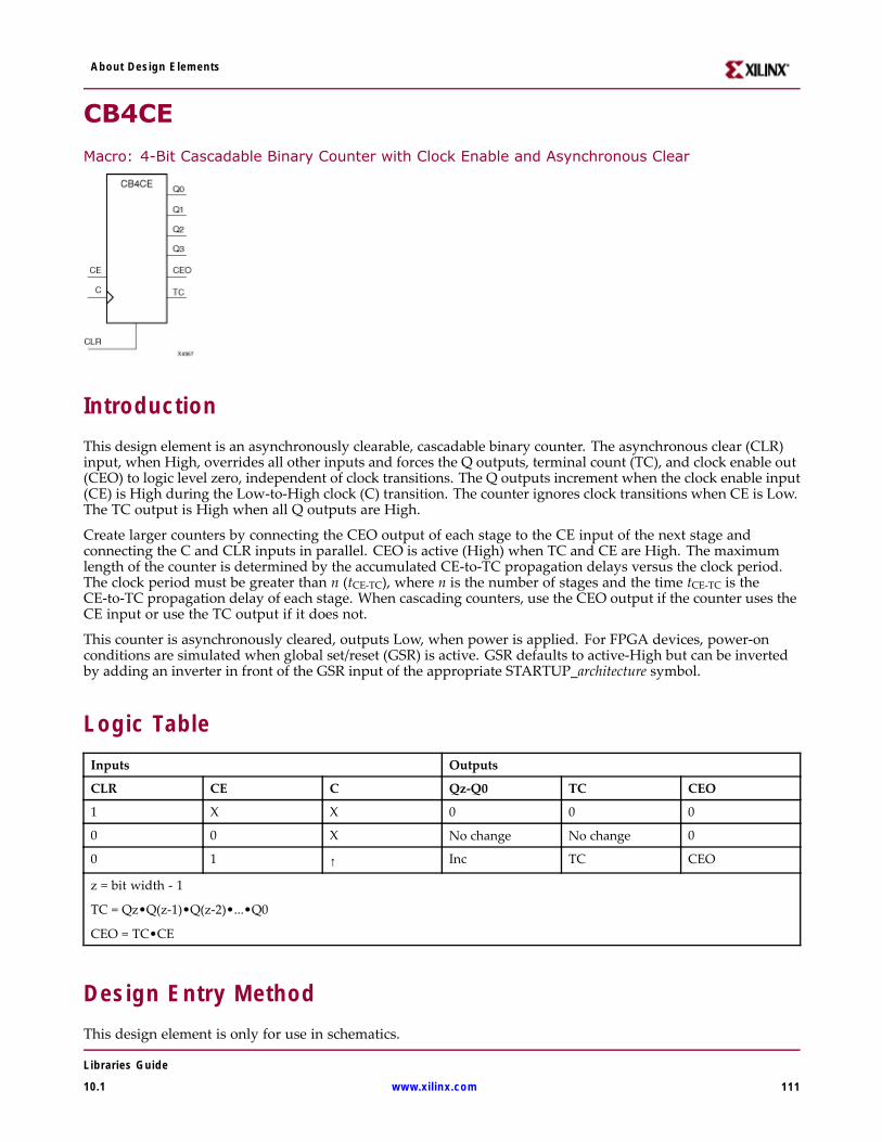
About Design Elements
CB4CE
Macro: 4-Bit Cascadable Binary Counter with Clock Enable and Asynchronous Clear
IntroductionThis design element is an asynchronously clearable, cascadable binary counter. The asynchronous clear (CLR)input, when High, overrides all other inputs and forces the Q outputs, terminal count (TC), and clock enable out(CEO) to logic level zero, independent of clock transitions. The Q outputs increment when the clock enable input(CE) is High during the Low-to-High clock (C) transition. The counter ignores clock transitions when CE is Low.The TC output is High when all Q outputs are High.
Create larger counters by connecting the CEO output of each stage to the CE input of the next stage andconnecting the C and CLR inputs in parallel. CEO is active (High) when TC and CE are High. The maximumlength of the counter is determined by the accumulated CE-to-TC propagation delays versus the clock period.The clock period must be greater than n (tCE-TC), where n is the number of stages and the time tCE-TC is theCE-to-TC propagation delay of each stage. When cascading counters, use the CEO output if the counter uses theCE input or use the TC output if it does not.
This counter is asynchronously cleared, outputs Low, when power is applied. For FPGA devices, power-onconditions are simulated when global set/reset (GSR) is active. GSR defaults to active-High but can be invertedby adding an inverter in front of the GSR input of the appropriate STARTUP_architecture symbol.
Logic TableInputs Outputs
CLR CE C Qz-Q0 TC CEO
1 X X 0 0 0
0 0 X No change No change 0
0 1 ↑ Inc TC CEO
z = bit width - 1
TC = Qz•Q(z-1)•Q(z-2)•...•Q0
CEO = TC•CE
Design Entry MethodThis design element is only for use in schematics.
Libraries Guide
10.1 www.xilinx.com 111

About Design Elements
For More Information• See the Virtex-4 User Guide.
• See the Virtex-4 Data Sheets.
Libraries Guide
112 www.xilinx.com 10.1
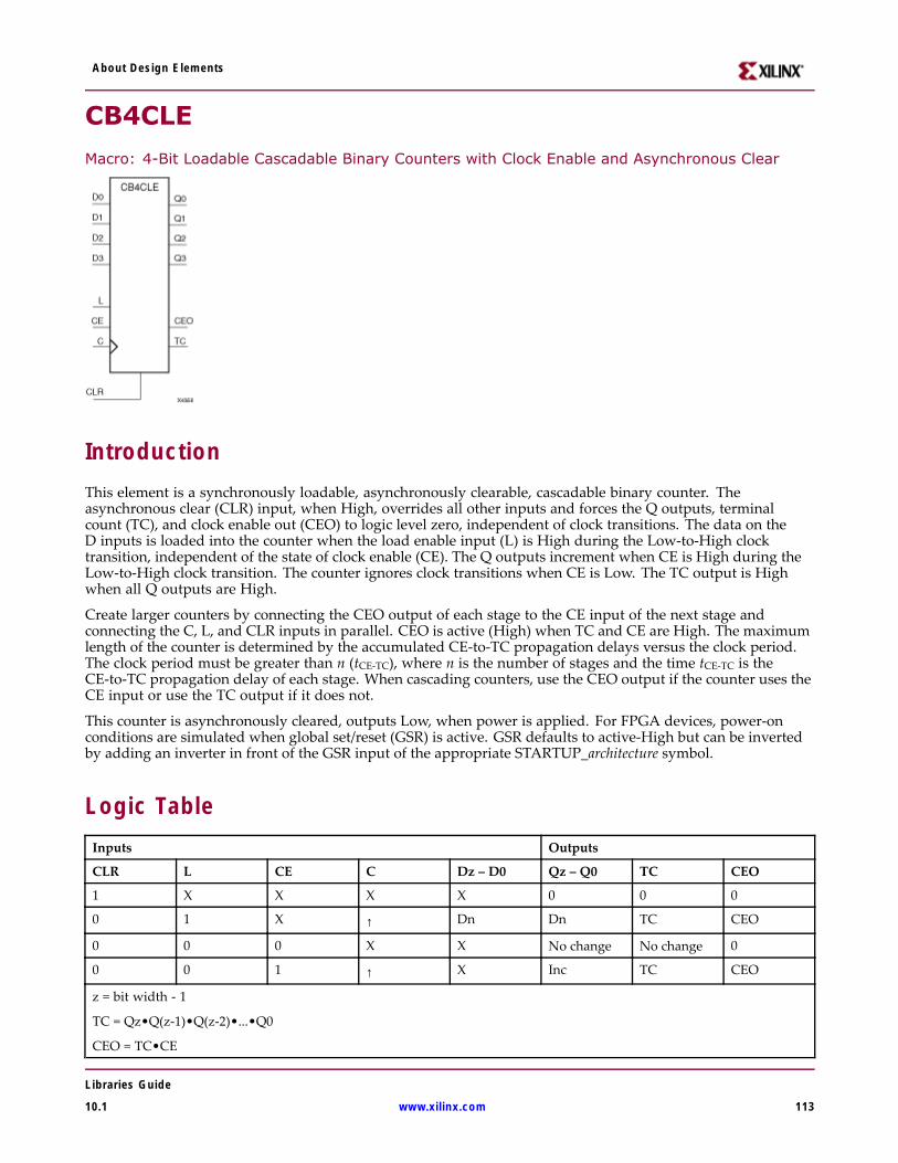
About Design Elements
CB4CLE
Macro: 4-Bit Loadable Cascadable Binary Counters with Clock Enable and Asynchronous Clear
IntroductionThis element is a synchronously loadable, asynchronously clearable, cascadable binary counter. Theasynchronous clear (CLR) input, when High, overrides all other inputs and forces the Q outputs, terminalcount (TC), and clock enable out (CEO) to logic level zero, independent of clock transitions. The data on theD inputs is loaded into the counter when the load enable input (L) is High during the Low-to-High clocktransition, independent of the state of clock enable (CE). The Q outputs increment when CE is High during theLow-to-High clock transition. The counter ignores clock transitions when CE is Low. The TC output is Highwhen all Q outputs are High.
Create larger counters by connecting the CEO output of each stage to the CE input of the next stage andconnecting the C, L, and CLR inputs in parallel. CEO is active (High) when TC and CE are High. The maximumlength of the counter is determined by the accumulated CE-to-TC propagation delays versus the clock period.The clock period must be greater than n (tCE-TC), where n is the number of stages and the time tCE-TC is theCE-to-TC propagation delay of each stage. When cascading counters, use the CEO output if the counter uses theCE input or use the TC output if it does not.
This counter is asynchronously cleared, outputs Low, when power is applied. For FPGA devices, power-onconditions are simulated when global set/reset (GSR) is active. GSR defaults to active-High but can be invertedby adding an inverter in front of the GSR input of the appropriate STARTUP_architecture symbol.
Logic TableInputs Outputs
CLR L CE C Dz – D0 Qz – Q0 TC CEO
1 X X X X 0 0 0
0 1 X ↑ Dn Dn TC CEO
0 0 0 X X No change No change 0
0 0 1 ↑ X Inc TC CEO
z = bit width - 1
TC = Qz•Q(z-1)•Q(z-2)•...•Q0
CEO = TC•CE
Libraries Guide
10.1 www.xilinx.com 113

About Design Elements
Design Entry MethodThis design element is only for use in schematics.
For More Information• See the Virtex-4 User Guide.
• See the Virtex-4 Data Sheets.
Libraries Guide
114 www.xilinx.com 10.1
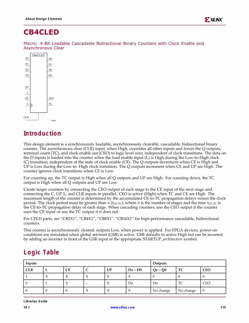
About Design Elements
CB4CLEDMacro: 4-Bit Loadable Cascadable Bidirectional Binary Counters with Clock Enable andAsynchronous Clear
IntroductionThis design element is a synchronously loadable, asynchronously clearable, cascadable, bidirectional binarycounter. The asynchronous clear (CLR) input, when High, overrides all other inputs and forces the Q outputs,terminal count (TC), and clock enable out (CEO) to logic level zero, independent of clock transitions. The data onthe D inputs is loaded into the counter when the load enable input (L) is High during the Low-to-High clock(C) transition, independent of the state of clock enable (CE). The Q outputs decrement when CE is High andUP is Low during the Low-to- High clock transition. The Q outputs increment when CE and UP are High. Thecounter ignores clock transitions when CE is Low.
For counting up, the TC output is High when all Q outputs and UP are High. For counting down, the TCoutput is High when all Q outputs and UP are Low.
Create larger counters by connecting the CEO output of each stage to the CE input of the next stage andconnecting the C, UP, L, and CLR inputs in parallel. CEO is active (High) when TC and CE are High. Themaximum length of the counter is determined by the accumulated CE-to-TC propagation delays versus the clockperiod. The clock period must be greater than n (tCE-TC), where n is the number of stages and the time tCE-TC isthe CE-to-TC propagation delay of each stage. When cascading counters, use the CEO output if the counteruses the CE input or use the TC output if it does not.
For CPLD parts, see “CB2X1”, “CB4X1”, “CB8X1”, “CB16X1” for high-performance cascadable, bidirectionalcounters.
This counter is asynchronously cleared, outputs Low, when power is applied. For FPGA devices, power-onconditions are simulated when global set/reset (GSR) is active. GSR defaults to active-High but can be invertedby adding an inverter in front of the GSR input of the appropriate STARTUP_architecture symbol.
Logic TableInputs Outputs
CLR L CE C UP Dz – D0 Qz – Q0 TC CEO
1 X X X X X 0 0 0
0 1 X ↑ X Dn Dn TC CEO
0 0 0 X X X No change No change 0
Libraries Guide
10.1 www.xilinx.com 115
About Design Elements
Inputs Outputs
CLR L CE C UP Dz – D0 Qz – Q0 TC CEO
0 0 1 ↑ 1 X Inc TC CEO
0 0 1 ↑ 0 X Dec TC CEO
z = bit width - 1
TC = (Qz•Q(z-1)•Q(z-2)•...•Q0•UP) + (Qz•Q(z-1)•Q(z-2)•...•Q0•UP)
CEO = TC•CE
Design Entry MethodThis design element is only for use in schematics.
For More Information• See the Virtex-4 User Guide.
• See the Virtex-4 Data Sheets.
Libraries Guide
116 www.xilinx.com 10.1
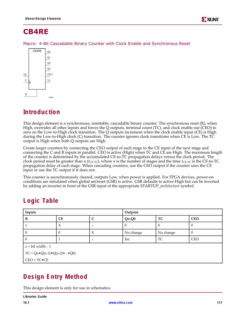
About Design Elements
CB4RE
Macro: 4-Bit Cascadable Binary Counter with Clock Enable and Synchronous Reset
IntroductionThis design element is a synchronous, resettable, cascadable binary counter. The synchronous reset (R), whenHigh, overrides all other inputs and forces the Q outputs, terminal count (TC), and clock enable out (CEO) tozero on the Low-to-High clock transition. The Q outputs increment when the clock enable input (CE) is Highduring the Low-to-High clock (C) transition. The counter ignores clock transitions when CE is Low. The TCoutput is High when both Q outputs are High.
Create larger counters by connecting the CEO output of each stage to the CE input of the next stage andconnecting the C and R inputs in parallel. CEO is active (High) when TC and CE are High. The maximum lengthof the counter is determined by the accumulated CE-to-TC propagation delays versus the clock period. Theclock period must be greater than n (tCE-TC), where n is the number of stages and the time tCE-TC is the CE-to-TCpropagation delay of each stage. When cascading counters, use the CEO output if the counter uses the CEinput or use the TC output if it does not.
This counter is asynchronously cleared, outputs Low, when power is applied. For FPGA devices, power-onconditions are simulated when global set/reset (GSR) is active. GSR defaults to active-High but can be invertedby adding an inverter in front of the GSR input of the appropriate STARTUP_architecture symbol.
Logic TableInputs Outputs
R CE C Qz-Q0 TC CEO
1 X ↑ 0 0 0
0 0 X No change No change 0
0 1 ↑ Inc TC CEO
z = bit width - 1
TC = Qz•Q(z-1)•Q(z-2)•...•Q0)
CEO = TC•CE
Design Entry MethodThis design element is only for use in schematics.
Libraries Guide
10.1 www.xilinx.com 117

About Design Elements
For More Information• See the Virtex-4 User Guide.
• See the Virtex-4 Data Sheets.
Libraries Guide
118 www.xilinx.com 10.1
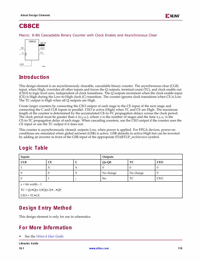
About Design Elements
CB8CEMacro: 8-Bit Cascadable Binary Counter with Clock Enable and Asynchronous Clear
IntroductionThis design element is an asynchronously clearable, cascadable binary counter. The asynchronous clear (CLR)input, when High, overrides all other inputs and forces the Q outputs, terminal count (TC), and clock enable out(CEO) to logic level zero, independent of clock transitions. The Q outputs increment when the clock enable input(CE) is High during the Low-to-High clock (C) transition. The counter ignores clock transitions when CE is Low.The TC output is High when all Q outputs are High.
Create larger counters by connecting the CEO output of each stage to the CE input of the next stage andconnecting the C and CLR inputs in parallel. CEO is active (High) when TC and CE are High. The maximumlength of the counter is determined by the accumulated CE-to-TC propagation delays versus the clock period.The clock period must be greater than n (tCE-TC), where n is the number of stages and the time tCE-TC is theCE-to-TC propagation delay of each stage. When cascading counters, use the CEO output if the counter uses theCE input or use the TC output if it does not.
This counter is asynchronously cleared, outputs Low, when power is applied. For FPGA devices, power-onconditions are simulated when global set/reset (GSR) is active. GSR defaults to active-High but can be invertedby adding an inverter in front of the GSR input of the appropriate STARTUP_architecture symbol.
Logic TableInputs Outputs
CLR CE C Qz-Q0 TC CEO
1 X X 0 0 0
0 0 X No change No change 0
0 1 ↑ Inc TC CEO
z = bit width - 1
TC = Qz•Q(z-1)•Q(z-2)•...•Q0
CEO = TC•CE
Design Entry MethodThis design element is only for use in schematics.
For More Information• See the Virtex-4 User Guide.
Libraries Guide
10.1 www.xilinx.com 119

About Design Elements
• See the Virtex-4 Data Sheets.
Libraries Guide
120 www.xilinx.com 10.1
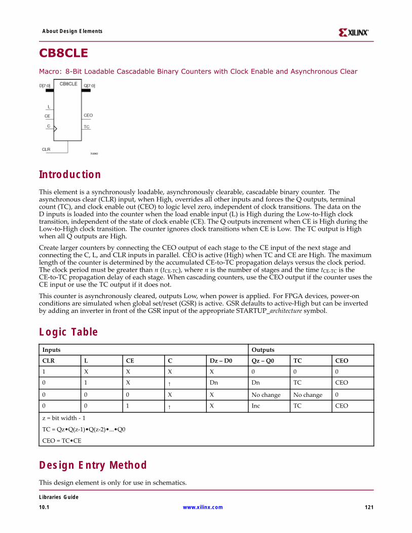
About Design Elements
CB8CLEMacro: 8-Bit Loadable Cascadable Binary Counters with Clock Enable and Asynchronous Clear
IntroductionThis element is a synchronously loadable, asynchronously clearable, cascadable binary counter. Theasynchronous clear (CLR) input, when High, overrides all other inputs and forces the Q outputs, terminalcount (TC), and clock enable out (CEO) to logic level zero, independent of clock transitions. The data on theD inputs is loaded into the counter when the load enable input (L) is High during the Low-to-High clocktransition, independent of the state of clock enable (CE). The Q outputs increment when CE is High during theLow-to-High clock transition. The counter ignores clock transitions when CE is Low. The TC output is Highwhen all Q outputs are High.
Create larger counters by connecting the CEO output of each stage to the CE input of the next stage andconnecting the C, L, and CLR inputs in parallel. CEO is active (High) when TC and CE are High. The maximumlength of the counter is determined by the accumulated CE-to-TC propagation delays versus the clock period.The clock period must be greater than n (tCE-TC), where n is the number of stages and the time tCE-TC is theCE-to-TC propagation delay of each stage. When cascading counters, use the CEO output if the counter uses theCE input or use the TC output if it does not.
This counter is asynchronously cleared, outputs Low, when power is applied. For FPGA devices, power-onconditions are simulated when global set/reset (GSR) is active. GSR defaults to active-High but can be invertedby adding an inverter in front of the GSR input of the appropriate STARTUP_architecture symbol.
Logic TableInputs Outputs
CLR L CE C Dz – D0 Qz – Q0 TC CEO
1 X X X X 0 0 0
0 1 X ↑ Dn Dn TC CEO
0 0 0 X X No change No change 0
0 0 1 ↑ X Inc TC CEO
z = bit width - 1
TC = Qz•Q(z-1)•Q(z-2)•...•Q0
CEO = TC•CE
Design Entry MethodThis design element is only for use in schematics.
Libraries Guide
10.1 www.xilinx.com 121

About Design Elements
For More Information• See the Virtex-4 User Guide.
• See the Virtex-4 Data Sheets.
Libraries Guide
122 www.xilinx.com 10.1

About Design Elements
CB8CLED
Macro: 8-Bit Loadable Cascadable Bidirectional Binary Counters with Clock Enable andAsynchronous Clear
IntroductionThis design element is a synchronously loadable, asynchronously clearable, cascadable, bidirectional binarycounter. The asynchronous clear (CLR) input, when High, overrides all other inputs and forces the Q outputs,terminal count (TC), and clock enable out (CEO) to logic level zero, independent of clock transitions. The data onthe D inputs is loaded into the counter when the load enable input (L) is High during the Low-to-High clock(C) transition, independent of the state of clock enable (CE). The Q outputs decrement when CE is High andUP is Low during the Low-to- High clock transition. The Q outputs increment when CE and UP are High. Thecounter ignores clock transitions when CE is Low.
For counting up, the TC output is High when all Q outputs and UP are High. For counting down, the TCoutput is High when all Q outputs and UP are Low.
Create larger counters by connecting the CEO output of each stage to the CE input of the next stage andconnecting the C, UP, L, and CLR inputs in parallel. CEO is active (High) when TC and CE are High. Themaximum length of the counter is determined by the accumulated CE-to-TC propagation delays versus the clockperiod. The clock period must be greater than n (tCE-TC), where n is the number of stages and the time tCE-TC isthe CE-to-TC propagation delay of each stage. When cascading counters, use the CEO output if the counteruses the CE input or use the TC output if it does not.
For CPLD parts, see “CB2X1”, “CB4X1”, “CB8X1”, “CB16X1” for high-performance cascadable, bidirectionalcounters.
This counter is asynchronously cleared, outputs Low, when power is applied. For FPGA devices, power-onconditions are simulated when global set/reset (GSR) is active. GSR defaults to active-High but can be invertedby adding an inverter in front of the GSR input of the appropriate STARTUP_architecture symbol.
Logic TableInputs Outputs
CLR L CE C UP Dz – D0 Qz – Q0 TC CEO
1 X X X X X 0 0 0
0 1 X ↑ X Dn Dn TC CEO
0 0 0 X X X No change No change 0
0 0 1 ↑ 1 X Inc TC CEO
Libraries Guide
10.1 www.xilinx.com 123

About Design Elements
Inputs Outputs
CLR L CE C UP Dz – D0 Qz – Q0 TC CEO
0 0 1 ↑ 0 X Dec TC CEO
z = bit width - 1
TC = (Qz•Q(z-1)•Q(z-2)•...•Q0•UP) + (Qz•Q(z-1)•Q(z-2)•...•Q0•UP)
CEO = TC•CE
Design Entry MethodThis design element is only for use in schematics.
For More Information• See the Virtex-4 User Guide.
• See the Virtex-4 Data Sheets.
Libraries Guide
124 www.xilinx.com 10.1

About Design Elements
CB8REMacro: 8-Bit Cascadable Binary Counter with Clock Enable and Synchronous Reset
IntroductionThis design element is a synchronous, resettable, cascadable binary counter. The synchronous reset (R), whenHigh, overrides all other inputs and forces the Q outputs, terminal count (TC), and clock enable out (CEO) tozero on the Low-to-High clock transition. The Q outputs increment when the clock enable input (CE) is Highduring the Low-to-High clock (C) transition. The counter ignores clock transitions when CE is Low. The TCoutput is High when both Q outputs are High.
Create larger counters by connecting the CEO output of each stage to the CE input of the next stage andconnecting the C and R inputs in parallel. CEO is active (High) when TC and CE are High. The maximum lengthof the counter is determined by the accumulated CE-to-TC propagation delays versus the clock period. Theclock period must be greater than n (tCE-TC), where n is the number of stages and the time tCE-TC is the CE-to-TCpropagation delay of each stage. When cascading counters, use the CEO output if the counter uses the CEinput or use the TC output if it does not.
This counter is asynchronously cleared, outputs Low, when power is applied. For FPGA devices, power-onconditions are simulated when global set/reset (GSR) is active. GSR defaults to active-High but can be invertedby adding an inverter in front of the GSR input of the appropriate STARTUP_architecture symbol.
Logic TableInputs Outputs
R CE C Qz-Q0 TC CEO
1 X ↑ 0 0 0
0 0 X No change No change 0
0 1 ↑ Inc TC CEO
z = bit width - 1
TC = Qz•Q(z-1)•Q(z-2)•...•Q0)
CEO = TC•CE
Design Entry MethodThis design element is only for use in schematics.
For More Information• See the Virtex-4 User Guide.
Libraries Guide
10.1 www.xilinx.com 125

About Design Elements
• See the Virtex-4 Data Sheets.
Libraries Guide
126 www.xilinx.com 10.1
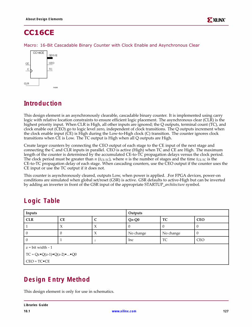
About Design Elements
CC16CE
Macro: 16-Bit Cascadable Binary Counter with Clock Enable and Asynchronous Clear
IntroductionThis design element is an asynchronously clearable, cascadable binary counter. It is implemented using carrylogic with relative location constraints to ensure efficient logic placement. The asynchronous clear (CLR) is thehighest priority input. When CLR is High, all other inputs are ignored; the Q outputs, terminal count (TC), andclock enable out (CEO) go to logic level zero, independent of clock transitions. The Q outputs increment whenthe clock enable input (CE) is High during the Low-to-High clock (C) transition. The counter ignores clocktransitions when CE is Low. The TC output is High when all Q outputs are High.
Create larger counters by connecting the CEO output of each stage to the CE input of the next stage andconnecting the C and CLR inputs in parallel. CEO is active (High) when TC and CE are High. The maximumlength of the counter is determined by the accumulated CE-to-TC propagation delays versus the clock period.The clock period must be greater than n (tCE-TC), where n is the number of stages and the time tCE-TC is theCE-to-TC propagation delay of each stage. When cascading counters, use the CEO output if the counter uses theCE input or use the TC output if it does not.
This counter is asynchronously cleared, outputs Low, when power is applied. .For FPGA devices, power-onconditions are simulated when global set/reset (GSR) is active. GSR defaults to active-High but can be invertedby adding an inverter in front of the GSR input of the appropriate STARTUP_architecture symbol.
Logic TableInputs Outputs
CLR CE C Qz-Q0 TC CEO
1 X X 0 0 0
0 0 X No change No change 0
0 1 ↑ Inc TC CEO
z = bit width - 1
TC = Qz•Q(z-1)•Q(z-2)•...•Q0
CEO = TC•CE
Design Entry MethodThis design element is only for use in schematics.
Libraries Guide
10.1 www.xilinx.com 127

About Design Elements
For More Information• See the Virtex-4 User Guide.
• See the Virtex-4 Data Sheets.
Libraries Guide
128 www.xilinx.com 10.1
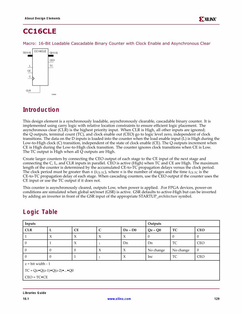
About Design Elements
CC16CLE
Macro: 16-Bit Loadable Cascadable Binary Counter with Clock Enable and Asynchronous Clear
IntroductionThis design element is a synchronously loadable, asynchronously clearable, cascadable binary counter. It isimplemented using carry logic with relative location constraints to ensure efficient logic placement. Theasynchronous clear (CLR) is the highest priority input. When CLR is High, all other inputs are ignored;the Q outputs, terminal count (TC), and clock enable out (CEO) go to logic level zero, independent of clocktransitions. The data on the D inputs is loaded into the counter when the load enable input (L) is High during theLow-to-High clock (C) transition, independent of the state of clock enable (CE). The Q outputs increment whenCE is High during the Low-to-High clock transition. The counter ignores clock transitions when CE is Low.The TC output is High when all Q outputs are High.
Create larger counters by connecting the CEO output of each stage to the CE input of the next stage andconnecting the C, L, and CLR inputs in parallel. CEO is active (High) when TC and CE are High. The maximumlength of the counter is determined by the accumulated CE-to-TC propagation delays versus the clock period.The clock period must be greater than n (tCE-TC), where n is the number of stages and the time tCE-TC is theCE-to-TC propagation delay of each stage. When cascading counters, use the CEO output if the counter uses theCE input or use the TC output if it does not.
This counter is asynchronously cleared, outputs Low, when power is applied. .For FPGA devices, power-onconditions are simulated when global set/reset (GSR) is active. GSR defaults to active-High but can be invertedby adding an inverter in front of the GSR input of the appropriate STARTUP_architecture symbol.
Logic TableInputs Outputs
CLR L CE C Dz – D0 Qz – Q0 TC CEO
1 X X X X 0 0 0
0 1 X ↑ Dn Dn TC CEO
0 0 0 X X No change No change 0
0 0 1 ↑ X Inc TC CEO
z = bit width - 1
TC = Qz•Q(z-1)•Q(z-2)•...•Q0
CEO = TC•CE
Libraries Guide
10.1 www.xilinx.com 129

About Design Elements
Design Entry MethodThis design element is only for use in schematics.
For More Information• See the Virtex-4 User Guide.
• See the Virtex-4 Data Sheets.
Libraries Guide
130 www.xilinx.com 10.1
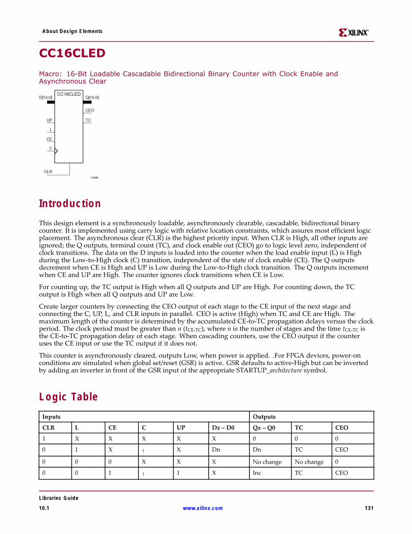
About Design Elements
CC16CLED
Macro: 16-Bit Loadable Cascadable Bidirectional Binary Counter with Clock Enable andAsynchronous Clear
IntroductionThis design element is a synchronously loadable, asynchronously clearable, cascadable, bidirectional binarycounter. It is implemented using carry logic with relative location constraints, which assures most efficient logicplacement. The asynchronous clear (CLR) is the highest priority input. When CLR is High, all other inputs areignored; the Q outputs, terminal count (TC), and clock enable out (CEO) go to logic level zero, independent ofclock transitions. The data on the D inputs is loaded into the counter when the load enable input (L) is Highduring the Low-to-High clock (C) transition, independent of the state of clock enable (CE). The Q outputsdecrement when CE is High and UP is Low during the Low-to-High clock transition. The Q outputs incrementwhen CE and UP are High. The counter ignores clock transitions when CE is Low.
For counting up, the TC output is High when all Q outputs and UP are High. For counting down, the TCoutput is High when all Q outputs and UP are Low.
Create larger counters by connecting the CEO output of each stage to the CE input of the next stage andconnecting the C, UP, L, and CLR inputs in parallel. CEO is active (High) when TC and CE are High. Themaximum length of the counter is determined by the accumulated CE-to-TC propagation delays versus the clockperiod. The clock period must be greater than n (tCE-TC), where n is the number of stages and the time tCE-TC isthe CE-to-TC propagation delay of each stage. When cascading counters, use the CEO output if the counteruses the CE input or use the TC output if it does not.
This counter is asynchronously cleared, outputs Low, when power is applied. .For FPGA devices, power-onconditions are simulated when global set/reset (GSR) is active. GSR defaults to active-High but can be invertedby adding an inverter in front of the GSR input of the appropriate STARTUP_architecture symbol.
Logic TableInputs Outputs
CLR L CE C UP Dz – D0 Qz – Q0 TC CEO
1 X X X X X 0 0 0
0 1 X ↑ X Dn Dn TC CEO
0 0 0 X X X No change No change 0
0 0 1 ↑ 1 X Inc TC CEO
Libraries Guide
10.1 www.xilinx.com 131

About Design Elements
Inputs Outputs
CLR L CE C UP Dz – D0 Qz – Q0 TC CEO
0 0 1 ↑ 0 X Dec TC CEO
z = bit width - 1
TC = (Qz•Q(z-1)•Q(z-2)•...•Q0•UP) + (Qz•Q(z-1)•Q(z-2)•...•Q0•UP)
CEO = TC•CE
Design Entry MethodThis design element is only for use in schematics.
For More Information• See the Virtex-4 User Guide.
• See the Virtex-4 Data Sheets.
Libraries Guide
132 www.xilinx.com 10.1
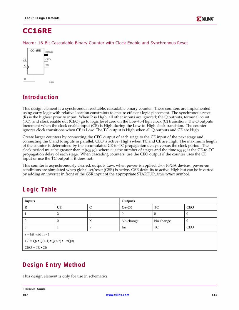
About Design Elements
CC16RE
Macro: 16-Bit Cascadable Binary Counter with Clock Enable and Synchronous Reset
IntroductionThis design element is a synchronous resettable, cascadable binary counter. These counters are implementedusing carry logic with relative location constraints to ensure efficient logic placement. The synchronous reset(R) is the highest priority input. When R is High, all other inputs are ignored; the Q outputs, terminal count(TC), and clock enable out (CEO) go to logic level zero on the Low-to-High clock (C) transition. The Q outputsincrement when the clock enable input (CE) is High during the Low-to-High clock transition. The counterignores clock transitions when CE is Low. The TC output is High when all Q outputs and CE are High.
Create larger counters by connecting the CEO output of each stage to the CE input of the next stage andconnecting the C and R inputs in parallel. CEO is active (High) when TC and CE are High. The maximum lengthof the counter is determined by the accumulated CE-to-TC propagation delays versus the clock period. Theclock period must be greater than n (tCE-TC), where n is the number of stages and the time tCE-TC is the CE-to-TCpropagation delay of each stage. When cascading counters, use the CEO output if the counter uses the CEinput or use the TC output if it does not.
This counter is asynchronously cleared, outputs Low, when power is applied. .For FPGA devices, power-onconditions are simulated when global set/reset (GSR) is active. GSR defaults to active-High but can be invertedby adding an inverter in front of the GSR input of the appropriate STARTUP_architecture symbol.
Logic TableInputs Outputs
R CE C Qz-Q0 TC CEO
1 X ↑ 0 0 0
0 0 X No change No change 0
0 1 ↑ Inc TC CEO
z = bit width - 1
TC = Qz•Q(z-1)•Q(z-2)•...•Q0)
CEO = TC•CE
Design Entry MethodThis design element is only for use in schematics.
Libraries Guide
10.1 www.xilinx.com 133

About Design Elements
For More Information• See the Virtex-4 User Guide.
• See the Virtex-4 Data Sheets.
Libraries Guide
134 www.xilinx.com 10.1
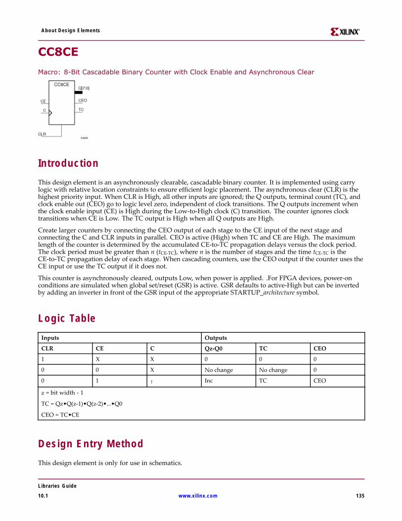
About Design Elements
CC8CE
Macro: 8-Bit Cascadable Binary Counter with Clock Enable and Asynchronous Clear
IntroductionThis design element is an asynchronously clearable, cascadable binary counter. It is implemented using carrylogic with relative location constraints to ensure efficient logic placement. The asynchronous clear (CLR) is thehighest priority input. When CLR is High, all other inputs are ignored; the Q outputs, terminal count (TC), andclock enable out (CEO) go to logic level zero, independent of clock transitions. The Q outputs increment whenthe clock enable input (CE) is High during the Low-to-High clock (C) transition. The counter ignores clocktransitions when CE is Low. The TC output is High when all Q outputs are High.
Create larger counters by connecting the CEO output of each stage to the CE input of the next stage andconnecting the C and CLR inputs in parallel. CEO is active (High) when TC and CE are High. The maximumlength of the counter is determined by the accumulated CE-to-TC propagation delays versus the clock period.The clock period must be greater than n (tCE-TC), where n is the number of stages and the time tCE-TC is theCE-to-TC propagation delay of each stage. When cascading counters, use the CEO output if the counter uses theCE input or use the TC output if it does not.
This counter is asynchronously cleared, outputs Low, when power is applied. .For FPGA devices, power-onconditions are simulated when global set/reset (GSR) is active. GSR defaults to active-High but can be invertedby adding an inverter in front of the GSR input of the appropriate STARTUP_architecture symbol.
Logic TableInputs Outputs
CLR CE C Qz-Q0 TC CEO
1 X X 0 0 0
0 0 X No change No change 0
0 1 ↑ Inc TC CEO
z = bit width - 1
TC = Qz•Q(z-1)•Q(z-2)•...•Q0
CEO = TC•CE
Design Entry MethodThis design element is only for use in schematics.
Libraries Guide
10.1 www.xilinx.com 135

About Design Elements
For More Information• See the Virtex-4 User Guide.
• See the Virtex-4 Data Sheets.
Libraries Guide
136 www.xilinx.com 10.1

About Design Elements
CC8CLE
Macro: 8-Bit Loadable Cascadable Binary Counter with Clock Enable and Asynchronous Clear
IntroductionThis design element is a synchronously loadable, asynchronously clearable, cascadable binary counter. It isimplemented using carry logic with relative location constraints to ensure efficient logic placement. Theasynchronous clear (CLR) is the highest priority input. When CLR is High, all other inputs are ignored;the Q outputs, terminal count (TC), and clock enable out (CEO) go to logic level zero, independent of clocktransitions. The data on the D inputs is loaded into the counter when the load enable input (L) is High during theLow-to-High clock (C) transition, independent of the state of clock enable (CE). The Q outputs increment whenCE is High during the Low-to-High clock transition. The counter ignores clock transitions when CE is Low.The TC output is High when all Q outputs are High.
Create larger counters by connecting the CEO output of each stage to the CE input of the next stage andconnecting the C, L, and CLR inputs in parallel. CEO is active (High) when TC and CE are High. The maximumlength of the counter is determined by the accumulated CE-to-TC propagation delays versus the clock period.The clock period must be greater than n (tCE-TC), where n is the number of stages and the time tCE-TC is theCE-to-TC propagation delay of each stage. When cascading counters, use the CEO output if the counter uses theCE input or use the TC output if it does not.
This counter is asynchronously cleared, outputs Low, when power is applied. .For FPGA devices, power-onconditions are simulated when global set/reset (GSR) is active. GSR defaults to active-High but can be invertedby adding an inverter in front of the GSR input of the appropriate STARTUP_architecture symbol.
Logic TableInputs Outputs
CLR L CE C Dz – D0 Qz – Q0 TC CEO
1 X X X X 0 0 0
0 1 X ↑ Dn Dn TC CEO
0 0 0 X X No change No change 0
0 0 1 ↑ X Inc TC CEO
z = bit width - 1
TC = Qz•Q(z-1)•Q(z-2)•...•Q0
CEO = TC•CE
Libraries Guide
10.1 www.xilinx.com 137

About Design Elements
Design Entry MethodThis design element is only for use in schematics.
For More Information• See the Virtex-4 User Guide.
• See the Virtex-4 Data Sheets.
Libraries Guide
138 www.xilinx.com 10.1
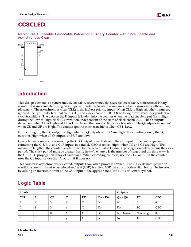
About Design Elements
CC8CLED
Macro: 8-Bit Loadable Cascadable Bidirectional Binary Counter with Clock Enable andAsynchronous Clear
IntroductionThis design element is a synchronously loadable, asynchronously clearable, cascadable, bidirectional binarycounter. It is implemented using carry logic with relative location constraints, which assures most efficient logicplacement. The asynchronous clear (CLR) is the highest priority input. When CLR is High, all other inputs areignored; the Q outputs, terminal count (TC), and clock enable out (CEO) go to logic level zero, independent ofclock transitions. The data on the D inputs is loaded into the counter when the load enable input (L) is Highduring the Low-to-High clock (C) transition, independent of the state of clock enable (CE). The Q outputsdecrement when CE is High and UP is Low during the Low-to-High clock transition. The Q outputs incrementwhen CE and UP are High. The counter ignores clock transitions when CE is Low.
For counting up, the TC output is High when all Q outputs and UP are High. For counting down, the TCoutput is High when all Q outputs and UP are Low.
Create larger counters by connecting the CEO output of each stage to the CE input of the next stage andconnecting the C, UP, L, and CLR inputs in parallel. CEO is active (High) when TC and CE are High. Themaximum length of the counter is determined by the accumulated CE-to-TC propagation delays versus the clockperiod. The clock period must be greater than n (tCE-TC), where n is the number of stages and the time tCE-TC isthe CE-to-TC propagation delay of each stage. When cascading counters, use the CEO output if the counteruses the CE input or use the TC output if it does not.
This counter is asynchronously cleared, outputs Low, when power is applied. .For FPGA devices, power-onconditions are simulated when global set/reset (GSR) is active. GSR defaults to active-High but can be invertedby adding an inverter in front of the GSR input of the appropriate STARTUP_architecture symbol.
Logic TableInputs Outputs
CLR L CE C UP Dz – D0 Qz – Q0 TC CEO
1 X X X X X 0 0 0
0 1 X ↑ X Dn Dn TC CEO
0 0 0 X X X No change No change 0
0 0 1 ↑ 1 X Inc TC CEO
Libraries Guide
10.1 www.xilinx.com 139
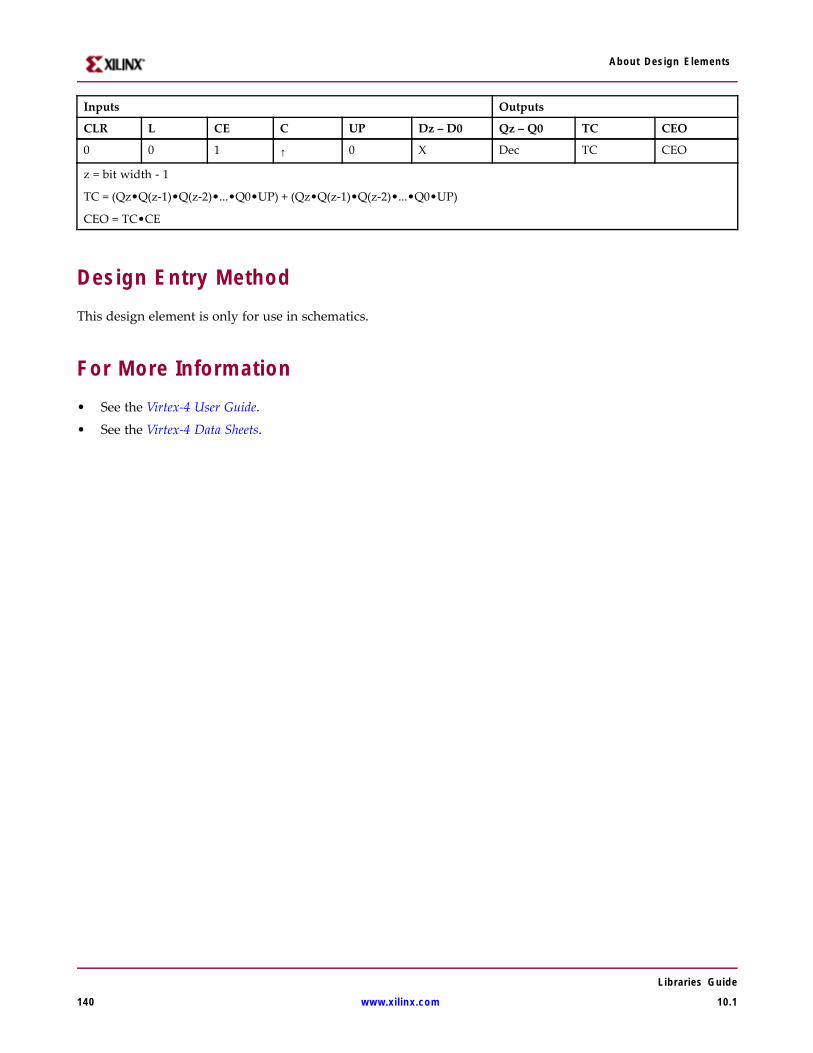
About Design Elements
Inputs Outputs
CLR L CE C UP Dz – D0 Qz – Q0 TC CEO
0 0 1 ↑ 0 X Dec TC CEO
z = bit width - 1
TC = (Qz•Q(z-1)•Q(z-2)•...•Q0•UP) + (Qz•Q(z-1)•Q(z-2)•...•Q0•UP)
CEO = TC•CE
Design Entry MethodThis design element is only for use in schematics.
For More Information• See the Virtex-4 User Guide.
• See the Virtex-4 Data Sheets.
Libraries Guide
140 www.xilinx.com 10.1
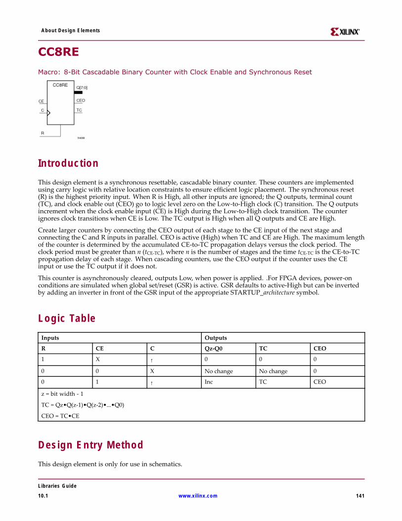
About Design Elements
CC8RE
Macro: 8-Bit Cascadable Binary Counter with Clock Enable and Synchronous Reset
IntroductionThis design element is a synchronous resettable, cascadable binary counter. These counters are implementedusing carry logic with relative location constraints to ensure efficient logic placement. The synchronous reset(R) is the highest priority input. When R is High, all other inputs are ignored; the Q outputs, terminal count(TC), and clock enable out (CEO) go to logic level zero on the Low-to-High clock (C) transition. The Q outputsincrement when the clock enable input (CE) is High during the Low-to-High clock transition. The counterignores clock transitions when CE is Low. The TC output is High when all Q outputs and CE are High.
Create larger counters by connecting the CEO output of each stage to the CE input of the next stage andconnecting the C and R inputs in parallel. CEO is active (High) when TC and CE are High. The maximum lengthof the counter is determined by the accumulated CE-to-TC propagation delays versus the clock period. Theclock period must be greater than n (tCE-TC), where n is the number of stages and the time tCE-TC is the CE-to-TCpropagation delay of each stage. When cascading counters, use the CEO output if the counter uses the CEinput or use the TC output if it does not.
This counter is asynchronously cleared, outputs Low, when power is applied. .For FPGA devices, power-onconditions are simulated when global set/reset (GSR) is active. GSR defaults to active-High but can be invertedby adding an inverter in front of the GSR input of the appropriate STARTUP_architecture symbol.
Logic TableInputs Outputs
R CE C Qz-Q0 TC CEO
1 X ↑ 0 0 0
0 0 X No change No change 0
0 1 ↑ Inc TC CEO
z = bit width - 1
TC = Qz•Q(z-1)•Q(z-2)•...•Q0)
CEO = TC•CE
Design Entry MethodThis design element is only for use in schematics.
Libraries Guide
10.1 www.xilinx.com 141

About Design Elements
For More Information• See the Virtex-4 User Guide.
• See the Virtex-4 Data Sheets.
Libraries Guide
142 www.xilinx.com 10.1
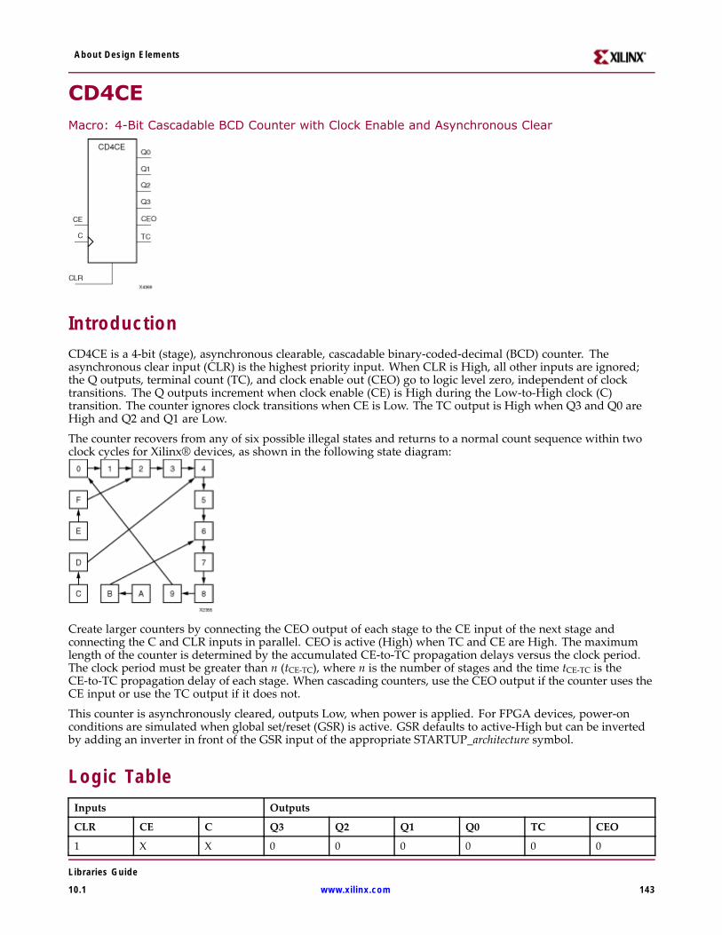
About Design Elements
CD4CEMacro: 4-Bit Cascadable BCD Counter with Clock Enable and Asynchronous Clear
IntroductionCD4CE is a 4-bit (stage), asynchronous clearable, cascadable binary-coded-decimal (BCD) counter. Theasynchronous clear input (CLR) is the highest priority input. When CLR is High, all other inputs are ignored;the Q outputs, terminal count (TC), and clock enable out (CEO) go to logic level zero, independent of clocktransitions. The Q outputs increment when clock enable (CE) is High during the Low-to-High clock (C)transition. The counter ignores clock transitions when CE is Low. The TC output is High when Q3 and Q0 areHigh and Q2 and Q1 are Low.
The counter recovers from any of six possible illegal states and returns to a normal count sequence within twoclock cycles for Xilinx® devices, as shown in the following state diagram:
Create larger counters by connecting the CEO output of each stage to the CE input of the next stage andconnecting the C and CLR inputs in parallel. CEO is active (High) when TC and CE are High. The maximumlength of the counter is determined by the accumulated CE-to-TC propagation delays versus the clock period.The clock period must be greater than n (tCE-TC), where n is the number of stages and the time tCE-TC is theCE-to-TC propagation delay of each stage. When cascading counters, use the CEO output if the counter uses theCE input or use the TC output if it does not.
This counter is asynchronously cleared, outputs Low, when power is applied. For FPGA devices, power-onconditions are simulated when global set/reset (GSR) is active. GSR defaults to active-High but can be invertedby adding an inverter in front of the GSR input of the appropriate STARTUP_architecture symbol.
Logic TableInputs Outputs
CLR CE C Q3 Q2 Q1 Q0 TC CEO
1 X X 0 0 0 0 0 0
Libraries Guide
10.1 www.xilinx.com 143
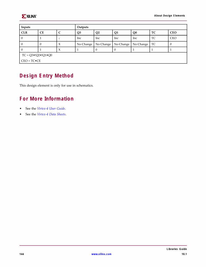
About Design Elements
Inputs Outputs
CLR CE C Q3 Q2 Q1 Q0 TC CEO
0 1 ↑ Inc Inc Inc Inc TC CEO
0 0 X No Change No Change No Change No Change TC 0
0 1 X 1 0 0 1 1 1
TC = Q3•!Q2•!Q1•Q0
CEO = TC•CE
Design Entry MethodThis design element is only for use in schematics.
For More Information• See the Virtex-4 User Guide.
• See the Virtex-4 Data Sheets.
Libraries Guide
144 www.xilinx.com 10.1
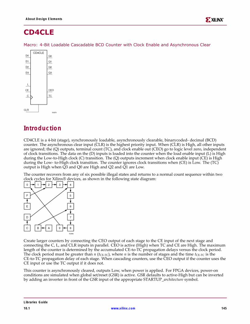
About Design Elements
CD4CLE
Macro: 4-Bit Loadable Cascadable BCD Counter with Clock Enable and Asynchronous Clear
IntroductionCD4CLE is a 4-bit (stage), synchronously loadable, asynchronously clearable, binarycoded- decimal (BCD)counter. The asynchronous clear input (CLR) is the highest priority input. When (CLR) is High, all other inputsare ignored; the (Q) outputs, terminal count (TC), and clock enable out (CEO) go to logic level zero, independentof clock transitions. The data on the (D) inputs is loaded into the counter when the load enable input (L) is Highduring the Low-to-High clock (C) transition. The (Q) outputs increment when clock enable input (CE) is Highduring the Low- to-High clock transition. The counter ignores clock transitions when (CE) is Low. The (TC)output is High when Q3 and Q0 are High and Q2 and Q1 are Low.
The counter recovers from any of six possible illegal states and returns to a normal count sequence within twoclock cycles for Xilinx® devices, as shown in the following state diagram:
Create larger counters by connecting the CEO output of each stage to the CE input of the next stage andconnecting the C, L, and CLR inputs in parallel. CEO is active (High) when TC and CE are High. The maximumlength of the counter is determined by the accumulated CE-to-TC propagation delays versus the clock period.The clock period must be greater than n (tCE-TC), where n is the number of stages and the time tCE-TC is theCE-to-TC propagation delay of each stage. When cascading counters, use the CEO output if the counter uses theCE input or use the TC output if it does not.
This counter is asynchronously cleared, outputs Low, when power is applied. For FPGA devices, power-onconditions are simulated when global set/reset (GSR) is active. GSR defaults to active-High but can be invertedby adding an inverter in front of the GSR input of the appropriate STARTUP_architecture symbol.
Libraries Guide
10.1 www.xilinx.com 145
About Design Elements
Logic TableInputs Outputs
CLR L CE D3 – D0 C Q3 Q2 Q1 Q0 TC CEO
1 X X X X 0 0 0 0 0 0
0 1 X D3 – D0 ↑ D3 D2 D1 D0 TC CEO
0 0 1 X ↑ Inc Inc Inc Inc TC CEO
0 0 0 X X NoChange
NoChange
NoChange
NoChange
TC 0
0 0 1 X X 1 0 0 1 1 1
TC = Q3•!Q2•!Q1•Q0
CEO = TC•CE
Design Entry MethodThis design element is only for use in schematics.
For More Information• See the Virtex-4 User Guide.
• See the Virtex-4 Data Sheets.
Libraries Guide
146 www.xilinx.com 10.1
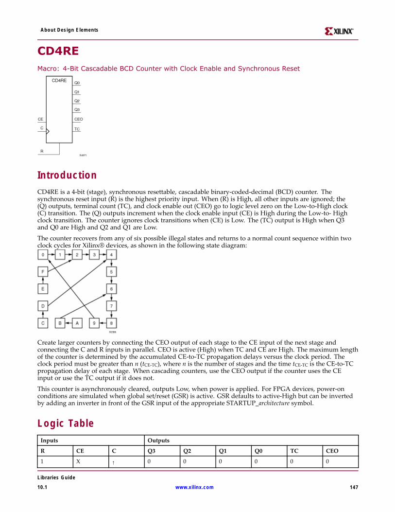
About Design Elements
CD4REMacro: 4-Bit Cascadable BCD Counter with Clock Enable and Synchronous Reset
IntroductionCD4RE is a 4-bit (stage), synchronous resettable, cascadable binary-coded-decimal (BCD) counter. Thesynchronous reset input (R) is the highest priority input. When (R) is High, all other inputs are ignored; the(Q) outputs, terminal count (TC), and clock enable out (CEO) go to logic level zero on the Low-to-High clock(C) transition. The (Q) outputs increment when the clock enable input (CE) is High during the Low-to- Highclock transition. The counter ignores clock transitions when (CE) is Low. The (TC) output is High when Q3and Q0 are High and Q2 and Q1 are Low.
The counter recovers from any of six possible illegal states and returns to a normal count sequence within twoclock cycles for Xilinx® devices, as shown in the following state diagram:
Create larger counters by connecting the CEO output of each stage to the CE input of the next stage andconnecting the C and R inputs in parallel. CEO is active (High) when TC and CE are High. The maximum lengthof the counter is determined by the accumulated CE-to-TC propagation delays versus the clock period. Theclock period must be greater than n (tCE-TC), where n is the number of stages and the time tCE-TC is the CE-to-TCpropagation delay of each stage. When cascading counters, use the CEO output if the counter uses the CEinput or use the TC output if it does not.
This counter is asynchronously cleared, outputs Low, when power is applied. For FPGA devices, power-onconditions are simulated when global set/reset (GSR) is active. GSR defaults to active-High but can be invertedby adding an inverter in front of the GSR input of the appropriate STARTUP_architecture symbol.
Logic TableInputs Outputs
R CE C Q3 Q2 Q1 Q0 TC CEO
1 X ↑ 0 0 0 0 0 0
Libraries Guide
10.1 www.xilinx.com 147
About Design Elements
Inputs Outputs
R CE C Q3 Q2 Q1 Q0 TC CEO
0 1 ↑ Inc Inc Inc Inc TC CEO
0 0 X No Change No Change No Change No Change TC 0
0 1 X 1 0 0 1 1 1
TC = Q3•!Q2•!Q1•Q0
CEO = TC•CE
Design Entry MethodThis design element is only for use in schematics.
For More Information• See the Virtex-4 User Guide.
• See the Virtex-4 Data Sheets.
Libraries Guide
148 www.xilinx.com 10.1
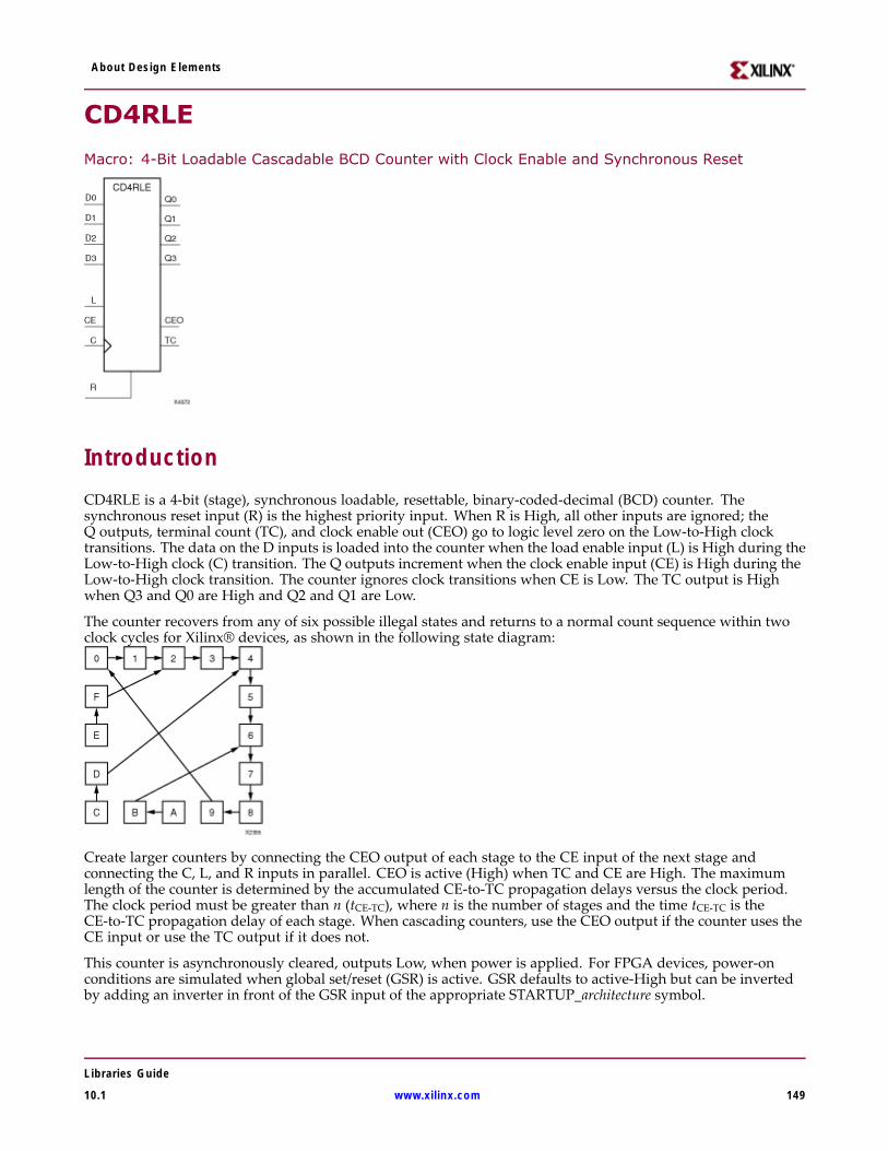
About Design Elements
CD4RLE
Macro: 4-Bit Loadable Cascadable BCD Counter with Clock Enable and Synchronous Reset
IntroductionCD4RLE is a 4-bit (stage), synchronous loadable, resettable, binary-coded-decimal (BCD) counter. Thesynchronous reset input (R) is the highest priority input. When R is High, all other inputs are ignored; theQ outputs, terminal count (TC), and clock enable out (CEO) go to logic level zero on the Low-to-High clocktransitions. The data on the D inputs is loaded into the counter when the load enable input (L) is High during theLow-to-High clock (C) transition. The Q outputs increment when the clock enable input (CE) is High during theLow-to-High clock transition. The counter ignores clock transitions when CE is Low. The TC output is Highwhen Q3 and Q0 are High and Q2 and Q1 are Low.
The counter recovers from any of six possible illegal states and returns to a normal count sequence within twoclock cycles for Xilinx® devices, as shown in the following state diagram:
Create larger counters by connecting the CEO output of each stage to the CE input of the next stage andconnecting the C, L, and R inputs in parallel. CEO is active (High) when TC and CE are High. The maximumlength of the counter is determined by the accumulated CE-to-TC propagation delays versus the clock period.The clock period must be greater than n (tCE-TC), where n is the number of stages and the time tCE-TC is theCE-to-TC propagation delay of each stage. When cascading counters, use the CEO output if the counter uses theCE input or use the TC output if it does not.
This counter is asynchronously cleared, outputs Low, when power is applied. For FPGA devices, power-onconditions are simulated when global set/reset (GSR) is active. GSR defaults to active-High but can be invertedby adding an inverter in front of the GSR input of the appropriate STARTUP_architecture symbol.
Libraries Guide
10.1 www.xilinx.com 149
About Design Elements
Logic TableInputs Outputs
R L CE D3 – D0 C Q3 Q2 Q1 Q0 TC CEO
1 X X X ↑ 0 0 0 0 0 0
0 1 X D3 – D0 ↑ D3 D D D0 TC CEO
0 0 1 X ↑ Inc Inc Inc Inc TC CEO
0 0 0 X X No Change NoChange
NoChange
NoChange
TC 0
0 0 1 X X 1 0 0 1 1 1
TC = Q3•!Q2•!Q1•Q0
CEO = TC•CE
Design Entry MethodThis design element is only for use in schematics.
For More Information• See the Virtex-4 User Guide.
• See the Virtex-4 Data Sheets.
Libraries Guide
150 www.xilinx.com 10.1

About Design Elements
CJ4CE
Macro: 4-Bit Johnson Counter with Clock Enable and Asynchronous Clear
IntroductionThis design element is a clearable Johnson/shift counter. The asynchronous clear (CLR) input, when High,overrides all other inputs and forces the data (Q) outputs to logic level zero, independent of clock (C) transitions.The counter increments (shifts Q0 to Q1, Q1 to Q2,and so forth) when the clock enable input (CE) is High duringthe Low-to-High clock transition. Clock transitions are ignored when (CE) is Low.
The Q3 output is inverted and fed back to input Q0 to provide continuous counting operation.
This counter is asynchronously cleared, outputs Low, when power is applied. For FPGA devices, power-onconditions are simulated when global set/reset (GSR) is active. GSR defaults to active-High but can be invertedby adding an inverter in front of the GSR input of the appropriate STARTUP_architecture symbol.
Logic TableInputs Outputs
CLR CE C Q0 Q1 through Q3
1 X X 0 0
0 0 X No change No change
0 1 ↑ !q3 q0 through q2
q = state of referenced output one setup time prior to active clock transition
Design Entry MethodThis design element is only for use in schematics.
For More Information• See the Virtex-4 User Guide.
• See the Virtex-4 Data Sheets.
Libraries Guide
10.1 www.xilinx.com 151

About Design Elements
CJ4RE
Macro: 4-Bit Johnson Counter with Clock Enable and Synchronous Reset
IntroductionThis design element is a resettable Johnson/shift counter. The synchronous reset (R) input, when High, overridesall other inputs and forces the data (Q) outputs to logic level zero during the Low-to-High clock (C) transition.The counter increments (shifts Q0 to Q1, Q1 to Q2, and so forth) when the clock enable input (CE) is High duringthe Low-to-High clock transition. Clock transitions are ignored when CE is Low.
The Q3 output is inverted and fed back to input Q0 to provide continuous counting operation.
This counter is asynchronously cleared, outputs Low, when power is applied. For FPGA devices, power-onconditions are simulated when global set/reset (GSR) is active. GSR defaults to active-High but can be invertedby adding an inverter in front of the GSR input of the appropriate STARTUP_architecture symbol.
Logic TableInputs Outputs
R CE C Q0 Q1 through Q3
1 X ↑ 0 0
0 0 X No change No change
0 1 ↑ !q3 q0 through q2
q = state of referenced output one setup time prior to active clock transition
Design Entry MethodThis design element is only for use in schematics.
For More Information• See the Virtex-4 User Guide.
• See the Virtex-4 Data Sheets.
Libraries Guide
152 www.xilinx.com 10.1
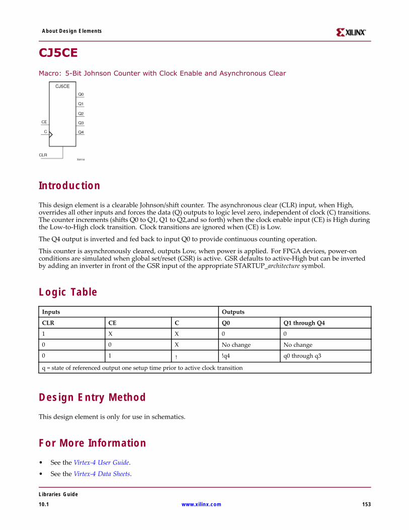
About Design Elements
CJ5CE
Macro: 5-Bit Johnson Counter with Clock Enable and Asynchronous Clear
IntroductionThis design element is a clearable Johnson/shift counter. The asynchronous clear (CLR) input, when High,overrides all other inputs and forces the data (Q) outputs to logic level zero, independent of clock (C) transitions.The counter increments (shifts Q0 to Q1, Q1 to Q2,and so forth) when the clock enable input (CE) is High duringthe Low-to-High clock transition. Clock transitions are ignored when (CE) is Low.
The Q4 output is inverted and fed back to input Q0 to provide continuous counting operation.
This counter is asynchronously cleared, outputs Low, when power is applied. For FPGA devices, power-onconditions are simulated when global set/reset (GSR) is active. GSR defaults to active-High but can be invertedby adding an inverter in front of the GSR input of the appropriate STARTUP_architecture symbol.
Logic TableInputs Outputs
CLR CE C Q0 Q1 through Q4
1 X X 0 0
0 0 X No change No change
0 1 ↑ !q4 q0 through q3
q = state of referenced output one setup time prior to active clock transition
Design Entry MethodThis design element is only for use in schematics.
For More Information• See the Virtex-4 User Guide.
• See the Virtex-4 Data Sheets.
Libraries Guide
10.1 www.xilinx.com 153
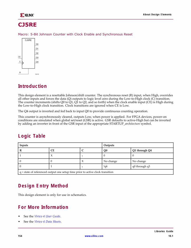
About Design Elements
CJ5RE
Macro: 5-Bit Johnson Counter with Clock Enable and Synchronous Reset
IntroductionThis design element is a resettable Johnson/shift counter. The synchronous reset (R) input, when High, overridesall other inputs and forces the data (Q) outputs to logic level zero during the Low-to-High clock (C) transition.The counter increments (shifts Q0 to Q1, Q1 to Q2, and so forth) when the clock enable input (CE) is High duringthe Low-to-High clock transition. Clock transitions are ignored when CE is Low.
The Q4 output is inverted and fed back to input Q0 to provide continuous counting operation.
This counter is asynchronously cleared, outputs Low, when power is applied. For FPGA devices, power-onconditions are simulated when global set/reset (GSR) is active. GSR defaults to active-High but can be invertedby adding an inverter in front of the GSR input of the appropriate STARTUP_architecture symbol.
Logic TableInputs Outputs
R CE C Q0 Q1 through Q4
1 X ↑ 0 0
0 0 X No change No change
0 1 ↑ !q4 q0 through q3
q = state of referenced output one setup time prior to active clock transition
Design Entry MethodThis design element is only for use in schematics.
For More Information• See the Virtex-4 User Guide.
• See the Virtex-4 Data Sheets.
Libraries Guide
154 www.xilinx.com 10.1
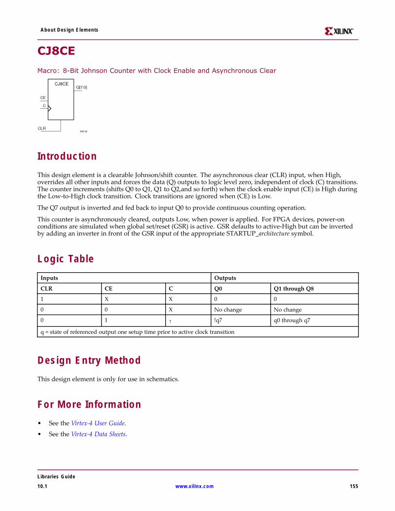
About Design Elements
CJ8CE
Macro: 8-Bit Johnson Counter with Clock Enable and Asynchronous Clear
IntroductionThis design element is a clearable Johnson/shift counter. The asynchronous clear (CLR) input, when High,overrides all other inputs and forces the data (Q) outputs to logic level zero, independent of clock (C) transitions.The counter increments (shifts Q0 to Q1, Q1 to Q2,and so forth) when the clock enable input (CE) is High duringthe Low-to-High clock transition. Clock transitions are ignored when (CE) is Low.
The Q7 output is inverted and fed back to input Q0 to provide continuous counting operation.
This counter is asynchronously cleared, outputs Low, when power is applied. For FPGA devices, power-onconditions are simulated when global set/reset (GSR) is active. GSR defaults to active-High but can be invertedby adding an inverter in front of the GSR input of the appropriate STARTUP_architecture symbol.
Logic TableInputs Outputs
CLR CE C Q0 Q1 through Q8
1 X X 0 0
0 0 X No change No change
0 1 ↑ !q7 q0 through q7
q = state of referenced output one setup time prior to active clock transition
Design Entry MethodThis design element is only for use in schematics.
For More Information• See the Virtex-4 User Guide.
• See the Virtex-4 Data Sheets.
Libraries Guide
10.1 www.xilinx.com 155

About Design Elements
CJ8RE
Macro: 8-Bit Johnson Counter with Clock Enable and Synchronous Reset
IntroductionThis design element is a resettable Johnson/shift counter. The synchronous reset (R) input, when High, overridesall other inputs and forces the data (Q) outputs to logic level zero during the Low-to-High clock (C) transition.The counter increments (shifts Q0 to Q1, Q1 to Q2, and so forth) when the clock enable input (CE) is High duringthe Low-to-High clock transition. Clock transitions are ignored when CE is Low.
The Q7 output is inverted and fed back to input Q0 to provide continuous counting operation.
This counter is asynchronously cleared, outputs Low, when power is applied. For FPGA devices, power-onconditions are simulated when global set/reset (GSR) is active. GSR defaults to active-High but can be invertedby adding an inverter in front of the GSR input of the appropriate STARTUP_architecture symbol.
Logic TableInputs Outputs
R CE C Q0 Q1 through Q7
1 X ↑ 0 0
0 0 X No change No change
0 1 ↑ !q7 q0 through q6
q = state of referenced output one setup time prior to active clock transition
Design Entry MethodThis design element is only for use in schematics.
For More Information• See the Virtex-4 User Guide.
• See the Virtex-4 Data Sheets.
Libraries Guide
156 www.xilinx.com 10.1
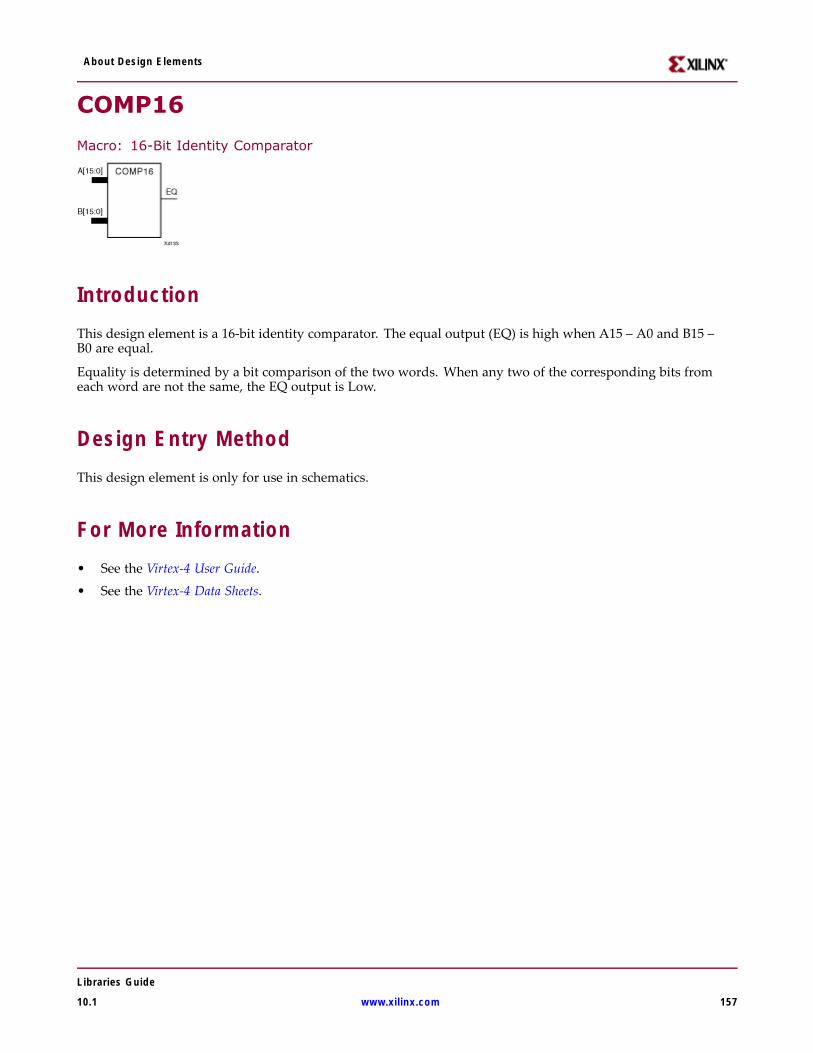
About Design Elements
COMP16
Macro: 16-Bit Identity Comparator
IntroductionThis design element is a 16-bit identity comparator. The equal output (EQ) is high when A15 – A0 and B15 –B0 are equal.
Equality is determined by a bit comparison of the two words. When any two of the corresponding bits fromeach word are not the same, the EQ output is Low.
Design Entry MethodThis design element is only for use in schematics.
For More Information• See the Virtex-4 User Guide.
• See the Virtex-4 Data Sheets.
Libraries Guide
10.1 www.xilinx.com 157
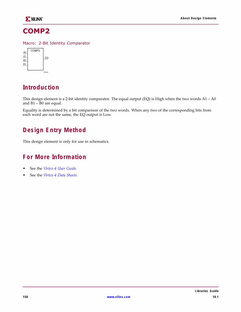
About Design Elements
COMP2
Macro: 2-Bit Identity Comparator
IntroductionThis design element is a 2-bit identity comparator. The equal output (EQ) is High when the two words A1 – A0and B1 – B0 are equal.
Equality is determined by a bit comparison of the two words. When any two of the corresponding bits fromeach word are not the same, the EQ output is Low.
Design Entry MethodThis design element is only for use in schematics.
For More Information• See the Virtex-4 User Guide.
• See the Virtex-4 Data Sheets.
Libraries Guide
158 www.xilinx.com 10.1

About Design Elements
COMP4
Macro: 4-Bit Identity Comparator
IntroductionThis design element is a 4-bit identity comparator. The equal output (EQ) is high when A3 – A0 and B3 –B0 are equal.
Equality is determined by a bit comparison of the two words. When any two of the corresponding bits fromeach word are not the same, the EQ output is Low.
Design Entry MethodThis design element is only for use in schematics.
For More Information• See the Virtex-4 User Guide.
• See the Virtex-4 Data Sheets.
Libraries Guide
10.1 www.xilinx.com 159
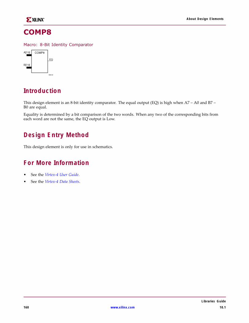
About Design Elements
COMP8
Macro: 8-Bit Identity Comparator
IntroductionThis design element is an 8-bit identity comparator. The equal output (EQ) is high when A7 – A0 and B7 –B0 are equal.
Equality is determined by a bit comparison of the two words. When any two of the corresponding bits fromeach word are not the same, the EQ output is Low.
Design Entry MethodThis design element is only for use in schematics.
For More Information• See the Virtex-4 User Guide.
• See the Virtex-4 Data Sheets.
Libraries Guide
160 www.xilinx.com 10.1
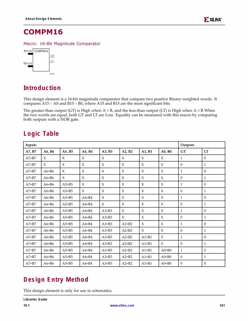
About Design Elements
COMPM16
Macro: 16-Bit Magnitude Comparator
IntroductionThis design element is a 16-bit magnitude comparator that compare two positive Binary-weighted words. Itcompares A15 – A0 and B15 – B0, where A15 and B15 are the most significant bits.
The greater-than output (GT) is High when A > B, and the less-than output (LT) is High when A < B Whenthe two words are equal, both GT and LT are Low. Equality can be measured with this macro by comparingboth outputs with a NOR gate.
Logic TableInputs Outputs
A7, B7 A6, B6 A5, B5 A4, B4 A3, B3 A2, B2 A1, B1 A0, B0 GT LT
A7>B7 X X X X X X X 1 0
A7<B7 X X X X X X X 0 1
A7=B7 A6>B6 X X X X X X 1 0
A7=B7 A6<B6 X X X X X X 0 1
A7=B7 A6=B6 A5>B5 X X X X X 1 0
A7=B7 A6=B6 A5<B5 X X X X X 0 1
A7=B7 A6=B6 A5=B5 A4>B4 X X X X 1 0
A7=B7 A6=B6 A5=B5 A4<B4 X X X X 0 1
A7=B7 A6=B6 A5=B5 A4=B4 A3>B3 X X X 1 0
A7=B7 A6=B6 A5=B5 A4=B4 A3<B3 X X X 0 1
A7=B7 A6=B6 A5=B5 A4=B4 A3=B3 A2>B2 X X 1 0
A7=B7 A6=B6 A5=B5 A4=B4 A3=B3 A2<B2 X X 0 1
A7=B7 A6=B6 A5=B5 A4=B4 A3=B3 A2=B2 A1>B1 X 1 0
A7=B7 A6=B6 A5=B5 A4=B4 A3=B3 A2=B2 A1<B1 X 0 1
A7=B7 A6=B6 A5=B5 A4=B4 A3=B3 A2=B2 A1=B1 A0>B0 1 0
A7=B7 A6=B6 A5=B5 A4=B4 A3=B3 A2=B2 A1=B1 A0<B0 0 1
A7=B7 A6=B6 A5=B5 A4=B4 A3=B3 A2=B2 A1=B1 A0=B0 0 0
Design Entry MethodThis design element is only for use in schematics.
Libraries Guide
10.1 www.xilinx.com 161

About Design Elements
For More Information• See the Virtex-4 User Guide.
• See the Virtex-4 Data Sheets.
Libraries Guide
162 www.xilinx.com 10.1
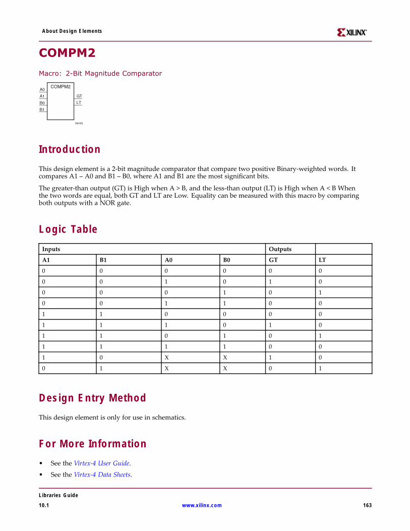
About Design Elements
COMPM2
Macro: 2-Bit Magnitude Comparator
IntroductionThis design element is a 2-bit magnitude comparator that compare two positive Binary-weighted words. Itcompares A1 – A0 and B1 – B0, where A1 and B1 are the most significant bits.
The greater-than output (GT) is High when A > B, and the less-than output (LT) is High when A < B Whenthe two words are equal, both GT and LT are Low. Equality can be measured with this macro by comparingboth outputs with a NOR gate.
Logic TableInputs Outputs
A1 B1 A0 B0 GT LT
0 0 0 0 0 0
0 0 1 0 1 0
0 0 0 1 0 1
0 0 1 1 0 0
1 1 0 0 0 0
1 1 1 0 1 0
1 1 0 1 0 1
1 1 1 1 0 0
1 0 X X 1 0
0 1 X X 0 1
Design Entry MethodThis design element is only for use in schematics.
For More Information• See the Virtex-4 User Guide.
• See the Virtex-4 Data Sheets.
Libraries Guide
10.1 www.xilinx.com 163
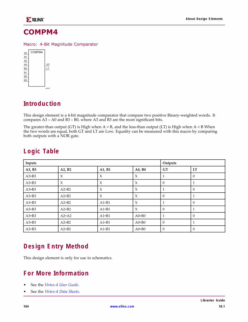
About Design Elements
COMPM4
Macro: 4-Bit Magnitude Comparator
IntroductionThis design element is a 4-bit magnitude comparator that compare two positive Binary-weighted words. Itcompares A3 – A0 and B3 – B0, where A3 and B3 are the most significant bits.
The greater-than output (GT) is High when A > B, and the less-than output (LT) is High when A < B Whenthe two words are equal, both GT and LT are Low. Equality can be measured with this macro by comparingboth outputs with a NOR gate.
Logic TableInputs Outputs
A3, B3 A2, B2 A1, B1 A0, B0 GT LT
A3>B3 X X X 1 0
A3<B3 X X X 0 1
A3=B3 A2>B2 X X 1 0
A3=B3 A2<B2 X X 0 1
A3=B3 A2=B2 A1>B1 X 1 0
A3=B3 A2=B2 A1<B1 X 0 1
A3=B3 A2=A2 A1=B1 A0>B0 1 0
A3=B3 A2=B2 A1=B1 A0<B0 0 1
A3=B3 A2=B2 A1=B1 A0=B0 0 0
Design Entry MethodThis design element is only for use in schematics.
For More Information• See the Virtex-4 User Guide.• See the Virtex-4 Data Sheets.
Libraries Guide
164 www.xilinx.com 10.1
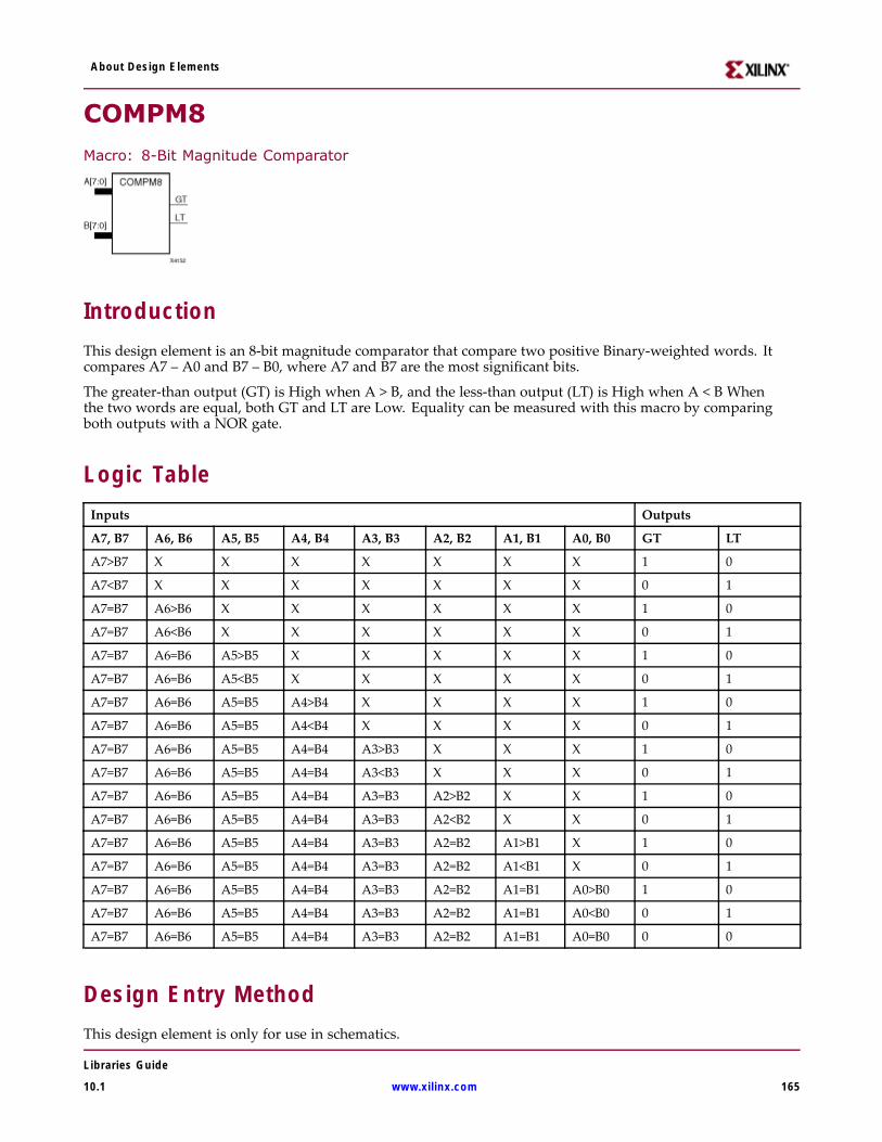
About Design Elements
COMPM8
Macro: 8-Bit Magnitude Comparator
IntroductionThis design element is an 8-bit magnitude comparator that compare two positive Binary-weighted words. Itcompares A7 – A0 and B7 – B0, where A7 and B7 are the most significant bits.
The greater-than output (GT) is High when A > B, and the less-than output (LT) is High when A < B Whenthe two words are equal, both GT and LT are Low. Equality can be measured with this macro by comparingboth outputs with a NOR gate.
Logic TableInputs Outputs
A7, B7 A6, B6 A5, B5 A4, B4 A3, B3 A2, B2 A1, B1 A0, B0 GT LT
A7>B7 X X X X X X X 1 0
A7<B7 X X X X X X X 0 1
A7=B7 A6>B6 X X X X X X 1 0
A7=B7 A6<B6 X X X X X X 0 1
A7=B7 A6=B6 A5>B5 X X X X X 1 0
A7=B7 A6=B6 A5<B5 X X X X X 0 1
A7=B7 A6=B6 A5=B5 A4>B4 X X X X 1 0
A7=B7 A6=B6 A5=B5 A4<B4 X X X X 0 1
A7=B7 A6=B6 A5=B5 A4=B4 A3>B3 X X X 1 0
A7=B7 A6=B6 A5=B5 A4=B4 A3<B3 X X X 0 1
A7=B7 A6=B6 A5=B5 A4=B4 A3=B3 A2>B2 X X 1 0
A7=B7 A6=B6 A5=B5 A4=B4 A3=B3 A2<B2 X X 0 1
A7=B7 A6=B6 A5=B5 A4=B4 A3=B3 A2=B2 A1>B1 X 1 0
A7=B7 A6=B6 A5=B5 A4=B4 A3=B3 A2=B2 A1<B1 X 0 1
A7=B7 A6=B6 A5=B5 A4=B4 A3=B3 A2=B2 A1=B1 A0>B0 1 0
A7=B7 A6=B6 A5=B5 A4=B4 A3=B3 A2=B2 A1=B1 A0<B0 0 1
A7=B7 A6=B6 A5=B5 A4=B4 A3=B3 A2=B2 A1=B1 A0=B0 0 0
Design Entry MethodThis design element is only for use in schematics.
Libraries Guide
10.1 www.xilinx.com 165

About Design Elements
For More Information• See the Virtex-4 User Guide.
• See the Virtex-4 Data Sheets.
Libraries Guide
166 www.xilinx.com 10.1
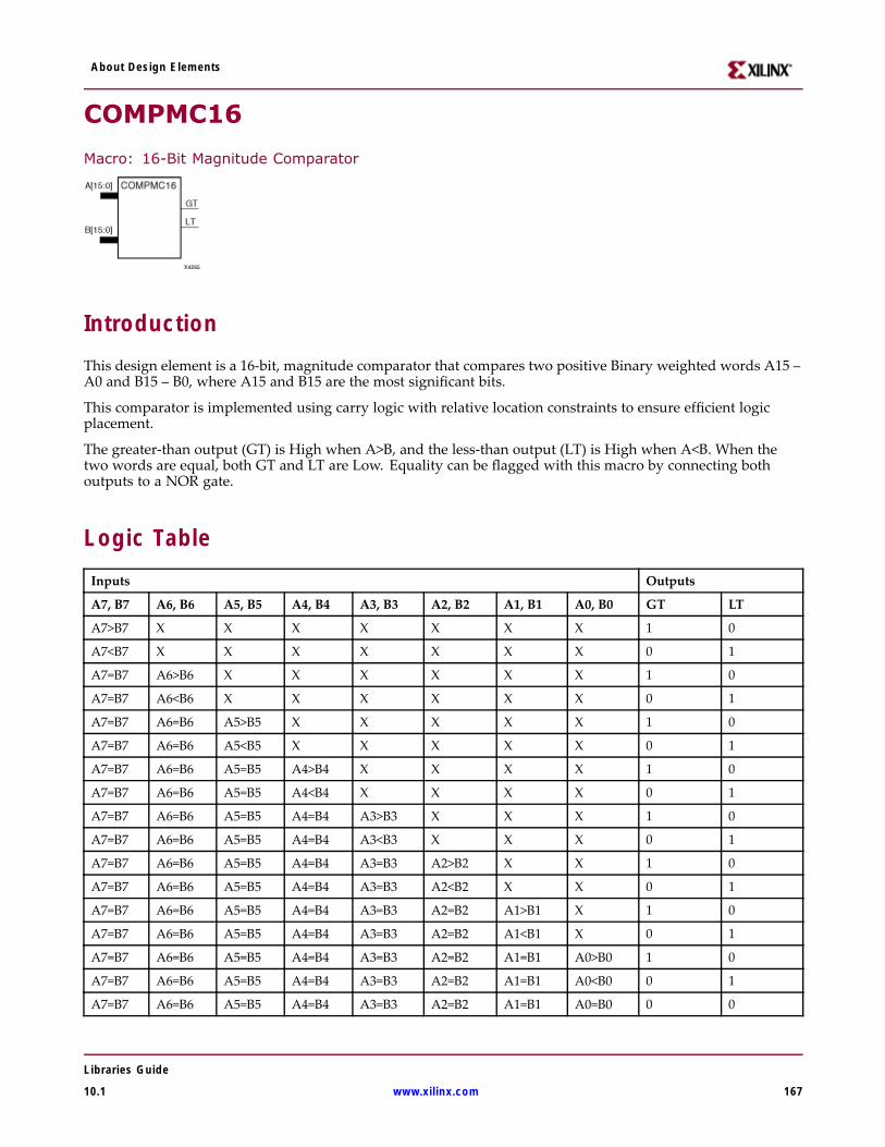
About Design Elements
COMPMC16
Macro: 16-Bit Magnitude Comparator
IntroductionThis design element is a 16-bit, magnitude comparator that compares two positive Binary weighted words A15 –A0 and B15 – B0, where A15 and B15 are the most significant bits.
This comparator is implemented using carry logic with relative location constraints to ensure efficient logicplacement.
The greater-than output (GT) is High when A>B, and the less-than output (LT) is High when A<B. When thetwo words are equal, both GT and LT are Low. Equality can be flagged with this macro by connecting bothoutputs to a NOR gate.
Logic TableInputs Outputs
A7, B7 A6, B6 A5, B5 A4, B4 A3, B3 A2, B2 A1, B1 A0, B0 GT LT
A7>B7 X X X X X X X 1 0
A7<B7 X X X X X X X 0 1
A7=B7 A6>B6 X X X X X X 1 0
A7=B7 A6<B6 X X X X X X 0 1
A7=B7 A6=B6 A5>B5 X X X X X 1 0
A7=B7 A6=B6 A5<B5 X X X X X 0 1
A7=B7 A6=B6 A5=B5 A4>B4 X X X X 1 0
A7=B7 A6=B6 A5=B5 A4<B4 X X X X 0 1
A7=B7 A6=B6 A5=B5 A4=B4 A3>B3 X X X 1 0
A7=B7 A6=B6 A5=B5 A4=B4 A3<B3 X X X 0 1
A7=B7 A6=B6 A5=B5 A4=B4 A3=B3 A2>B2 X X 1 0
A7=B7 A6=B6 A5=B5 A4=B4 A3=B3 A2<B2 X X 0 1
A7=B7 A6=B6 A5=B5 A4=B4 A3=B3 A2=B2 A1>B1 X 1 0
A7=B7 A6=B6 A5=B5 A4=B4 A3=B3 A2=B2 A1<B1 X 0 1
A7=B7 A6=B6 A5=B5 A4=B4 A3=B3 A2=B2 A1=B1 A0>B0 1 0
A7=B7 A6=B6 A5=B5 A4=B4 A3=B3 A2=B2 A1=B1 A0<B0 0 1
A7=B7 A6=B6 A5=B5 A4=B4 A3=B3 A2=B2 A1=B1 A0=B0 0 0
Libraries Guide
10.1 www.xilinx.com 167

About Design Elements
Design Entry MethodThis design element is only for use in schematics.
For More Information• See the Virtex-4 User Guide.
• See the Virtex-4 Data Sheets.
Libraries Guide
168 www.xilinx.com 10.1
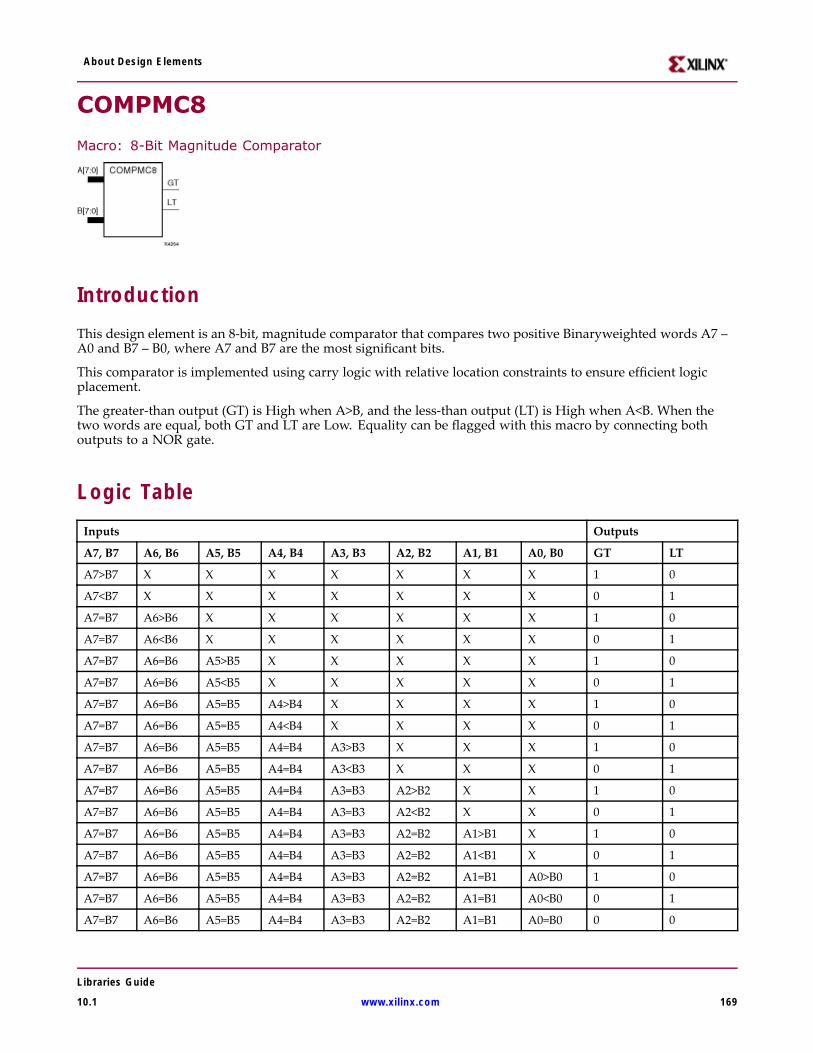
About Design Elements
COMPMC8
Macro: 8-Bit Magnitude Comparator
IntroductionThis design element is an 8-bit, magnitude comparator that compares two positive Binaryweighted words A7 –A0 and B7 – B0, where A7 and B7 are the most significant bits.
This comparator is implemented using carry logic with relative location constraints to ensure efficient logicplacement.
The greater-than output (GT) is High when A>B, and the less-than output (LT) is High when A<B. When thetwo words are equal, both GT and LT are Low. Equality can be flagged with this macro by connecting bothoutputs to a NOR gate.
Logic TableInputs Outputs
A7, B7 A6, B6 A5, B5 A4, B4 A3, B3 A2, B2 A1, B1 A0, B0 GT LT
A7>B7 X X X X X X X 1 0
A7<B7 X X X X X X X 0 1
A7=B7 A6>B6 X X X X X X 1 0
A7=B7 A6<B6 X X X X X X 0 1
A7=B7 A6=B6 A5>B5 X X X X X 1 0
A7=B7 A6=B6 A5<B5 X X X X X 0 1
A7=B7 A6=B6 A5=B5 A4>B4 X X X X 1 0
A7=B7 A6=B6 A5=B5 A4<B4 X X X X 0 1
A7=B7 A6=B6 A5=B5 A4=B4 A3>B3 X X X 1 0
A7=B7 A6=B6 A5=B5 A4=B4 A3<B3 X X X 0 1
A7=B7 A6=B6 A5=B5 A4=B4 A3=B3 A2>B2 X X 1 0
A7=B7 A6=B6 A5=B5 A4=B4 A3=B3 A2<B2 X X 0 1
A7=B7 A6=B6 A5=B5 A4=B4 A3=B3 A2=B2 A1>B1 X 1 0
A7=B7 A6=B6 A5=B5 A4=B4 A3=B3 A2=B2 A1<B1 X 0 1
A7=B7 A6=B6 A5=B5 A4=B4 A3=B3 A2=B2 A1=B1 A0>B0 1 0
A7=B7 A6=B6 A5=B5 A4=B4 A3=B3 A2=B2 A1=B1 A0<B0 0 1
A7=B7 A6=B6 A5=B5 A4=B4 A3=B3 A2=B2 A1=B1 A0=B0 0 0
Libraries Guide
10.1 www.xilinx.com 169

About Design Elements
Design Entry MethodThis design element is only for use in schematics.
For More Information• See the Virtex-4 User Guide.
• See the Virtex-4 Data Sheets.
Libraries Guide
170 www.xilinx.com 10.1
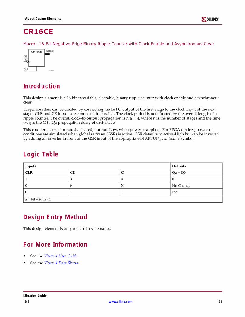
About Design Elements
CR16CE
Macro: 16-Bit Negative-Edge Binary Ripple Counter with Clock Enable and Asynchronous Clear
IntroductionThis design element is a 16-bit cascadable, clearable, binary ripple counter with clock enable and asynchronousclear.
Larger counters can be created by connecting the last Q output of the first stage to the clock input of the nextstage. CLR and CE inputs are connected in parallel. The clock period is not affected by the overall length of aripple counter. The overall clock-to-output propagation is n(tC - Q), where n is the number of stages and the timetC - Q is the C-to-Qz propagation delay of each stage.
This counter is asynchronously cleared, outputs Low, when power is applied. For FPGA devices, power-onconditions are simulated when global set/reset (GSR) is active. GSR defaults to active-High but can be invertedby adding an inverter in front of the GSR input of the appropriate STARTUP_architecture symbol.
Logic TableInputs Outputs
CLR CE C Qz – Q0
1 X X 0
0 0 X No Change
0 1 ↓ Inc
z = bit width - 1
Design Entry MethodThis design element is only for use in schematics.
For More Information• See the Virtex-4 User Guide.
• See the Virtex-4 Data Sheets.
Libraries Guide
10.1 www.xilinx.com 171
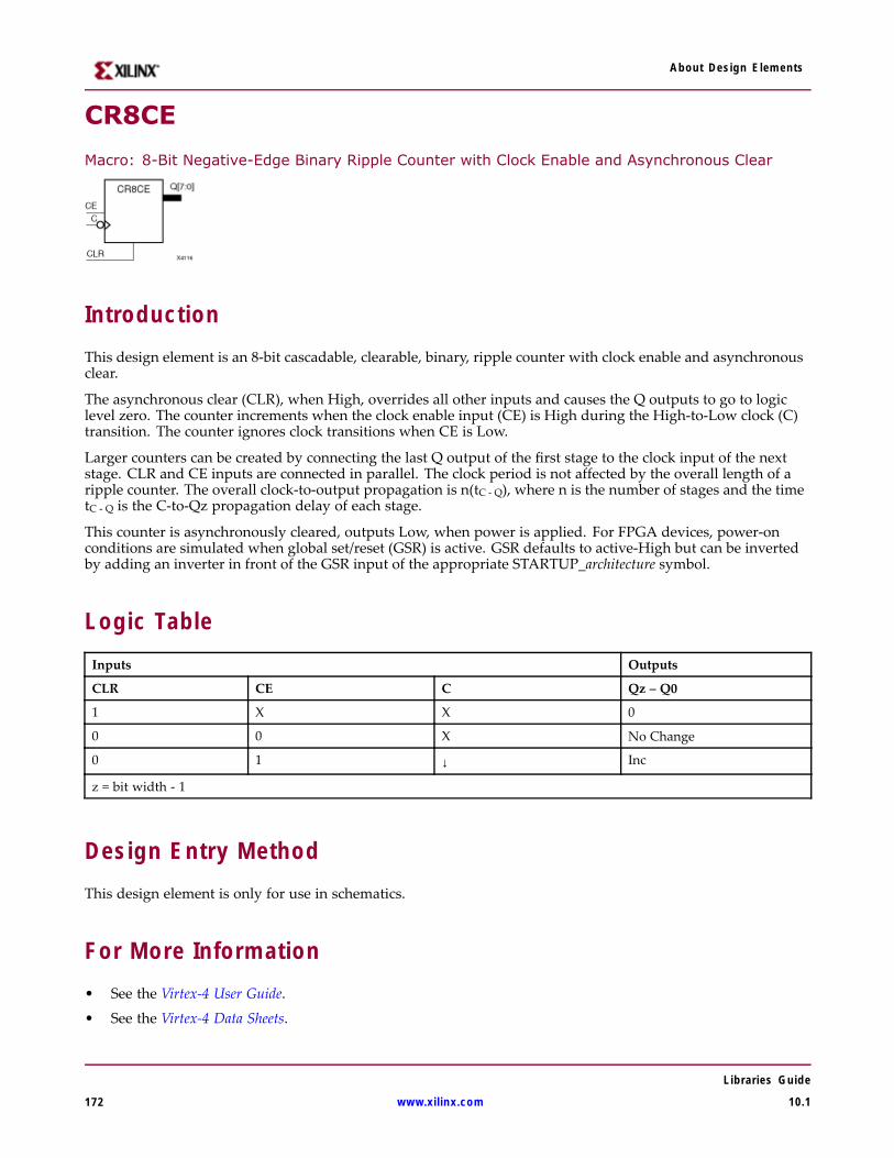
About Design Elements
CR8CE
Macro: 8-Bit Negative-Edge Binary Ripple Counter with Clock Enable and Asynchronous Clear
IntroductionThis design element is an 8-bit cascadable, clearable, binary, ripple counter with clock enable and asynchronousclear.
The asynchronous clear (CLR), when High, overrides all other inputs and causes the Q outputs to go to logiclevel zero. The counter increments when the clock enable input (CE) is High during the High-to-Low clock (C)transition. The counter ignores clock transitions when CE is Low.
Larger counters can be created by connecting the last Q output of the first stage to the clock input of the nextstage. CLR and CE inputs are connected in parallel. The clock period is not affected by the overall length of aripple counter. The overall clock-to-output propagation is n(tC - Q), where n is the number of stages and the timetC - Q is the C-to-Qz propagation delay of each stage.
This counter is asynchronously cleared, outputs Low, when power is applied. For FPGA devices, power-onconditions are simulated when global set/reset (GSR) is active. GSR defaults to active-High but can be invertedby adding an inverter in front of the GSR input of the appropriate STARTUP_architecture symbol.
Logic TableInputs Outputs
CLR CE C Qz – Q0
1 X X 0
0 0 X No Change
0 1 ↓ Inc
z = bit width - 1
Design Entry MethodThis design element is only for use in schematics.
For More Information• See the Virtex-4 User Guide.
• See the Virtex-4 Data Sheets.
Libraries Guide
172 www.xilinx.com 10.1
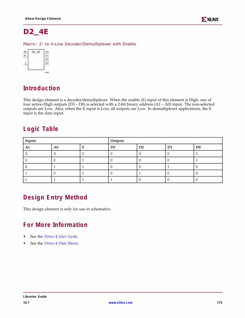
About Design Elements
D2_4E
Macro: 2- to 4-Line Decoder/Demultiplexer with Enable
IntroductionThis design element is a decoder/demultiplexer. When the enable (E) input of this element is High, one offour active-High outputs (D3 – D0) is selected with a 2-bit binary address (A1 – A0) input. The non-selectedoutputs are Low. Also, when the E input is Low, all outputs are Low. In demultiplexer applications, the Einput is the data input.
Logic TableInputs Outputs
A1 A0 E D3 D2 D1 D0
X X 0 0 0 0 0
0 0 1 0 0 0 1
0 1 1 0 0 1 0
1 0 1 0 1 0 0
1 1 1 1 0 0 0
Design Entry MethodThis design element is only for use in schematics.
For More Information• See the Virtex-4 User Guide.
• See the Virtex-4 Data Sheets.
Libraries Guide
10.1 www.xilinx.com 173
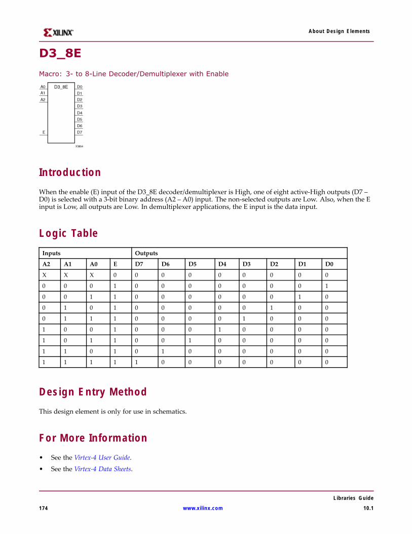
About Design Elements
D3_8E
Macro: 3- to 8-Line Decoder/Demultiplexer with Enable
IntroductionWhen the enable (E) input of the D3_8E decoder/demultiplexer is High, one of eight active-High outputs (D7 –D0) is selected with a 3-bit binary address (A2 – A0) input. The non-selected outputs are Low. Also, when the Einput is Low, all outputs are Low. In demultiplexer applications, the E input is the data input.
Logic TableInputs Outputs
A2 A1 A0 E D7 D6 D5 D4 D3 D2 D1 D0
X X X 0 0 0 0 0 0 0 0 0
0 0 0 1 0 0 0 0 0 0 0 1
0 0 1 1 0 0 0 0 0 0 1 0
0 1 0 1 0 0 0 0 0 1 0 0
0 1 1 1 0 0 0 0 1 0 0 0
1 0 0 1 0 0 0 1 0 0 0 0
1 0 1 1 0 0 1 0 0 0 0 0
1 1 0 1 0 1 0 0 0 0 0 0
1 1 1 1 1 0 0 0 0 0 0 0
Design Entry MethodThis design element is only for use in schematics.
For More Information• See the Virtex-4 User Guide.
• See the Virtex-4 Data Sheets.
Libraries Guide
174 www.xilinx.com 10.1
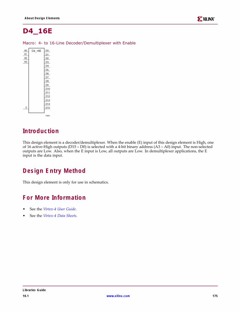
About Design Elements
D4_16E
Macro: 4- to 16-Line Decoder/Demultiplexer with Enable
IntroductionThis design element is a decoder/demultiplexer. When the enable (E) input of this design element is High, oneof 16 active-High outputs (D15 – D0) is selected with a 4-bit binary address (A3 – A0) input. The non-selectedoutputs are Low. Also, when the E input is Low, all outputs are Low. In demultiplexer applications, the Einput is the data input.
Design Entry MethodThis design element is only for use in schematics.
For More Information• See the Virtex-4 User Guide.
• See the Virtex-4 Data Sheets.
Libraries Guide
10.1 www.xilinx.com 175
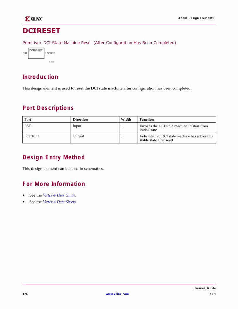
About Design Elements
DCIRESET
Primitive: DCI State Machine Reset (After Configuration Has Been Completed)
IntroductionThis design element is used to reset the DCI state machine after configuration has been completed.
Port DescriptionsPort Direction Width Function
RST Input 1 Invokes the DCI state machine to start frominitial state
LOCKED Output 1 Indicates that DCI state machine has achieved astable state after reset
Design Entry MethodThis design element can be used in schematics.
For More Information• See the Virtex-4 User Guide.
• See the Virtex-4 Data Sheets.
Libraries Guide
176 www.xilinx.com 10.1
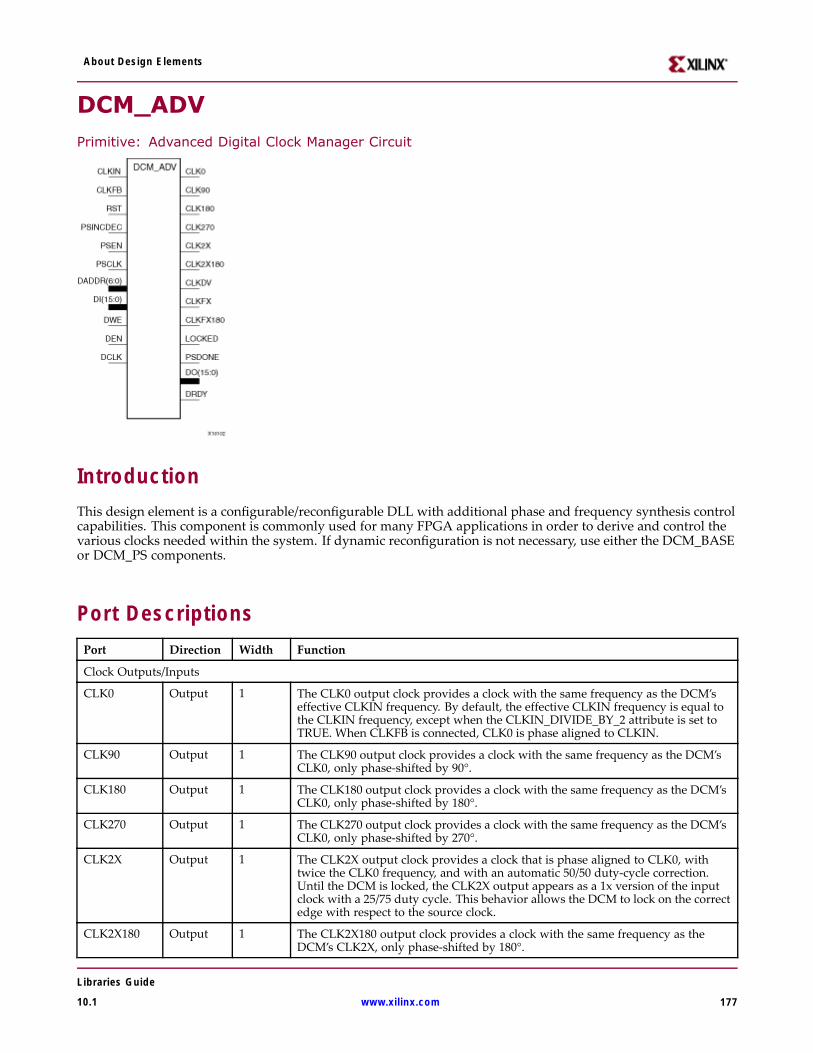
About Design Elements
DCM_ADVPrimitive: Advanced Digital Clock Manager Circuit
IntroductionThis design element is a configurable/reconfigurable DLL with additional phase and frequency synthesis controlcapabilities. This component is commonly used for many FPGA applications in order to derive and control thevarious clocks needed within the system. If dynamic reconfiguration is not necessary, use either the DCM_BASEor DCM_PS components.
Port DescriptionsPort Direction Width Function
Clock Outputs/Inputs
CLK0 Output 1 The CLK0 output clock provides a clock with the same frequency as the DCM’seffective CLKIN frequency. By default, the effective CLKIN frequency is equal tothe CLKIN frequency, except when the CLKIN_DIVIDE_BY_2 attribute is set toTRUE. When CLKFB is connected, CLK0 is phase aligned to CLKIN.
CLK90 Output 1 The CLK90 output clock provides a clock with the same frequency as the DCM’sCLK0, only phase-shifted by 90°.
CLK180 Output 1 The CLK180 output clock provides a clock with the same frequency as the DCM’sCLK0, only phase-shifted by 180°.
CLK270 Output 1 The CLK270 output clock provides a clock with the same frequency as the DCM’sCLK0, only phase-shifted by 270°.
CLK2X Output 1 The CLK2X output clock provides a clock that is phase aligned to CLK0, withtwice the CLK0 frequency, and with an automatic 50/50 duty-cycle correction.Until the DCM is locked, the CLK2X output appears as a 1x version of the inputclock with a 25/75 duty cycle. This behavior allows the DCM to lock on the correctedge with respect to the source clock.
CLK2X180 Output 1 The CLK2X180 output clock provides a clock with the same frequency as theDCM’s CLK2X, only phase-shifted by 180°.
Libraries Guide
10.1 www.xilinx.com 177
About Design Elements
Port Direction Width Function
CLKDV Output 1 The frequency divide (CLKDV) output clock provides a clock that is phase alignedto CLK0 with a frequency that is a fraction of the effective CLKIN frequency.The fraction is determined by the CLKDV_DIVIDE attribute. By default, theeffective CLKIN frequency is equal to the CLKIN frequency, except when theCLKIN_DIVIDE_BY_2 attribute is set to TRUE.
CLKFX Output 1 The frequency (CLKFX) output clock provides a clock with the followingfrequency definition:
CLKFX Frequency = (M/D) x (Effective CLKIN Frequency).
In this equation, M is the multiplier (numerator), with a value defined by theCLKFX_MULTIPLY attribute. D is the divisor (denominator), with a value definedby the CLKFX_DIVIDE attribute. Specifications for M and D, as well as input andoutput frequency ranges for the frequency synthesizer, are provided in the DataSheet for this architecture. The rising edge of CLKFX output is phase aligned tothe rising edges of CLK0, CLK2X, and CLKDV when the feedback path (CLKFB) isused. When M and D do have no common factor, the alignment occurs only onceevery D cycles of CLK0. By default, the effective CLKIN frequency is equal to theCLKIN frequency, except when the CLKIN_DIVIDE_BY_2 attribute is set to TRUE.
CLKFX180 Output 1 The CLKFX180 output clock provides a clock with the same frequency as theDCM’s CLKFX only phase-shifted by 180°.
CLKIN Input 1 The source clock (CLKIN) input pin provides the source clock to the DCM. TheCLKIN frequency must fall in the ranges specified in the Data Sheet for thisarchitecture. The clock input signal comes from one of the following buffers:
1. IBUFG - Global Clock Input Buffer. The DCM compensates for the clock inputpath when an IBUFG, on the same edge (top or bottom) of the device, such asthe DCM, is used.
2. BUFG/BUFGCTRL - Internal Global Clock Buffer. Any BUFGCTRL can driveany DCM in the Virtex-5 device using the dedicated global routing. A BUFGCTRLcan drive the DCM CLKIN pin when used to connect two DCM in series.
3. IBUF - Input Buffer. When IBUF drives CLKIN input, the PAD to DCM inputskew is not compensated and increased jitter can occur. This configuration isgenerally not recommended.
CLKFB Input 1 The feedback clock (CLKFB) input pin provides a reference or feedback signal tothe DCM to delay-compensate the clock outputs and align it with the clock input.To provide the necessary feedback to the DCM, connect only the CLK0 output tothe CLKFB input via a BUFG component in the case of internal feedback or anOBUF ’ IBUFG to the case of external feedback. Set the CLK_FEEDBACK attributeto 1X. When the CLKFB pin is connected, CLK0, CLKDV, and CLKFX are phasealigned to CLKIN. When the CLKFB pin is not connected, set CLK_FEEDBACKto NONE and only the CLKFX and CLKFX180 outputs are valid, however, notphase aligned to CLKIN.
Status Outputs / Control Inputs
LOCKED Output 1 Synchronous output from the PLL that provides you with an indication that thePLL has achieved phase alignment and is ready for operation.
PSDONE Output 1 Dynamic CLKIN select input. When high, ’1’ CLKIN1 is selected and whilelow, ’0’ CLKIN2 is selected. If dual clock selection is not necessary, connect thisinput to a logic 1.
Libraries Guide
178 www.xilinx.com 10.1
About Design Elements
Port Direction Width Function
RST Input 1 The reset (RST) input pin resets the DCM circuitry. The RST signal is an activeHigh asynchronous reset. Asserting the RST signal asynchronously forces allDCM outputs Low (the LOCKED signal, all status signals, and all output clockswithin four source clock cycles). Because the reset is asynchronous, the last cycleof the clocks can exhibit an unintended short pulse, severely distorted duty-cycle,and no longer phase adjust with respect to one another while deasserting. The RSTpin must be used when reconfiguring the device or changing the input frequency.Deasserting the RST signal synchronously starts the locking process at the nextCLKIN cycle. To ensure a proper DCM reset and locking process, the RST signalmust be deasserted after the CLKIN signal has been present and stable for at leastthree clock cycles. In all designs, the DCM must be held in reset until the clock isstable. During configuration, the DCM is automatically held in reset until GSR isreleased. If the clock is stable when GSR is released.
PSCLK Input 1 The phase-shift clock (PSCLK) input pin provides the source clock for the DCMphase shift. The phase-shift clock signal can be driven by any clock source(external or internal).
The frequency range of PSCLK is defined by PSCLK_FREQ_LF/HF (see theData Sheet for this architecture). This input must be tied to ground when theCLKOUT_PHASE_SHIFT attribute is set to NONE or FIXED.
PSINCDEC Input 1 The PSINCDEC input signal is synchronous with PSCLK. The PSINCDECinput signal is used to increment or decrement the phase-shift factor whenCLKOUT_PHASE_SHIFT is set to one of the variable modes. As a result, theoutput clock is phase shifted. the PSINCDEC signal is asserted High for increment,or deasserted Low for decrement. This input must be tied to ground when theCLKOUT_PHASE_SHIFT attribute is set to NONE or FIXED.
PSEN Input 1 The PSEN input signal is synchronous with PSCLK. A variable phase-shiftoperation is initiated by the PSEN input signal when CLKOUT_PHASE_SHIFT isset to a variable mode. It must be activated for one period of PSCLK. After PSENis initiated, the phase change is effective for up to 100 CLKIN pulse cycles, plusthree PSCLK cycles, and is indicated by a High pulse on PSDONE. There are nosporadic changes or glitches on any output during the phase transition. From thetime PSEN is enabled until PSDONE is flagged, the DCM output clock movesbit-by-bit from its original phase shift to the target phase shift. The phase-shiftis complete when PSDONE is flagged. PSEN must be tied to ground when theCLKOUT_PHASE_SHIFT attribute is set to NONE or FIXED.
Dynamic Reconfiguration / DCM Status
For more information on Dynamic Configuration, please see the Configuration User Guide.
DO Output 16 The DO output bus provides DCM status when not using the dynamicreconfiguration feature, and a data output when using the dynamicreconfiguration. When showing DCM status, the following mapping applies:
DO[0] - Phase-shift overflow
DO[1] CLKIN stopped
DO[2] - CLKFX stopped
DO[3] - CLKFB stopped
DO[15:4] - Not assigned
DRDY Output 1 The DRDY output pin provides ready status for the DCM’s dynamicreconfiguration feature
DI Input 16 The DI input bus provides reconfiguration data for dynamic reconfiguration.When not used, all bits must be assigned zeros.
DADDR Input 7 The DADDR input bus provides a reconfiguration address for dynamicreconfiguration. When not used, all bits must be assigned zeros.
Libraries Guide
10.1 www.xilinx.com 179
About Design Elements
Port Direction Width Function
DWE Input 1 The DWE input pin provides the write enable control signal to write the DI datainto the DADDR address. When not used, it must be tied Low.
DEN Input 1 The DEN input pin provides the enable control signal to access the dynamicreconfiguration feature. To reflect the DCM status signals on the DO output bus,when not used, it should be tied to High because if DEN is tied Low, DO alwaysoutputs a Low signal.
DCLK Input 1 The DCLK input pin provides the source clock for the DCM’s dynamicreconfiguration circuit. The frequency of DCLK can be asynchronous (in phaseand frequency) to CLKIN. The dynamic reconfiguration clock signal is driven byany clock source. The frequency range of DCLK is described in the Data Sheet forthis architecture. When dynamic reconfiguration is not used, this input mustbe tied to ground.
Design Entry MethodThis design element can be used in schematics.
Available AttributesAttribute Type Allowed Values Default Description
CLK_FEEDBACK String "1X" , "2X",or "NONE"
“1X” Specifies the clock feedbackof the allowed value.
CLKDV_DIVIDE Float 1.5, 2.0, 2.5, 3.0, 3.5, 4.0,4.5, 5.0, 5.5, 6.0, 6.5, 7.0,7.5, 8.0, 9.0, 10.0, 11.0,12.0, 13.0, 14.0, 15.0 or16.0
2.0 Specifies the extent to whichthe CLKDLL, CLKDLLE,CLKDLLHF, or DCM clockdivider (CLKDV output) is tobe frequency divided.
CLKFX_DIVIDE Integer 1 to 32 1 Specifies the frequencydivider value for the CLKFXoutput.
CLKFX_MULTIPLY Integer 2 to 32 4 Specifies the frequencymultiplier value for theCLKFX output.
CLKIN_DIVIDE_ BY_2 Boolean FALSE, TRUE FALSE Allows for the input clockfrequency to be divided inhalf when such a reductionis necessary to meet theDCM input clock frequencyrequirements.
CLKIN_PERIOD Float 1.25 to 1000.00 0.0 Specifies period of inputclock in ns from 1.25 to1000.00.
CLKOUT_ PHASE_SHIFT
String "NONE","FIXED","VARIABLE_POSITIVE","VARIABLE_ CENTER"or "DIRECT"
"NONE” Specifies the phase shiftmode of allowed value.
Libraries Guide
180 www.xilinx.com 10.1
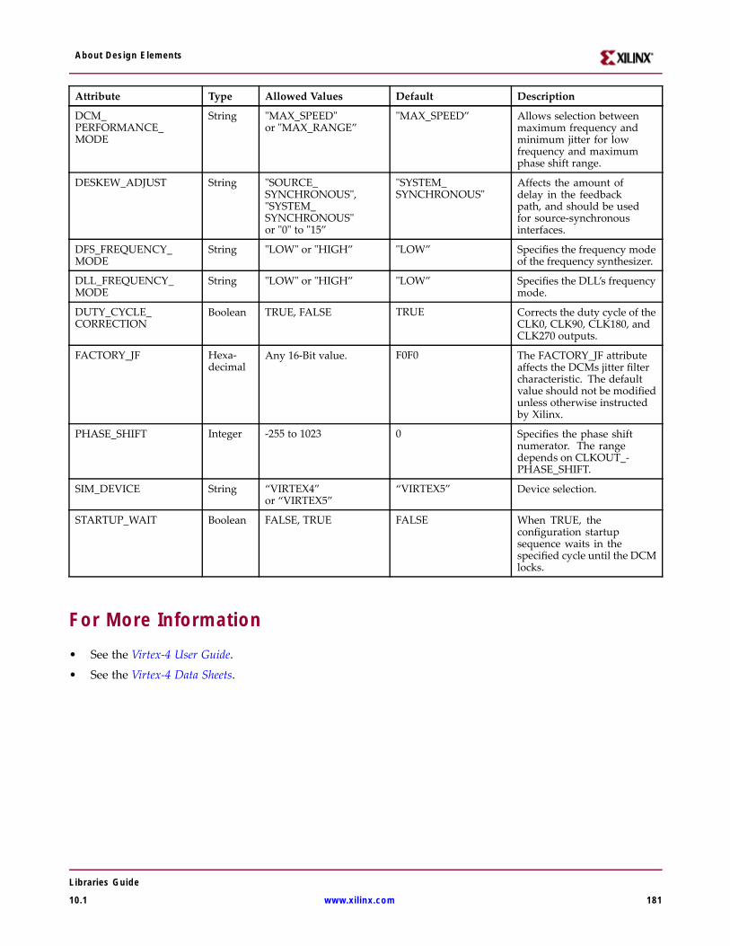
About Design Elements
Attribute Type Allowed Values Default Description
DCM_PERFORMANCE_MODE
String "MAX_SPEED"or "MAX_RANGE”
"MAX_SPEED” Allows selection betweenmaximum frequency andminimum jitter for lowfrequency and maximumphase shift range.
DESKEW_ADJUST String "SOURCE_SYNCHRONOUS","SYSTEM_SYNCHRONOUS"or "0" to "15”
"SYSTEM_SYNCHRONOUS"
Affects the amount ofdelay in the feedbackpath, and should be usedfor source-synchronousinterfaces.
DFS_FREQUENCY_MODE
String "LOW" or "HIGH” "LOW” Specifies the frequency modeof the frequency synthesizer.
DLL_FREQUENCY_MODE
String "LOW" or "HIGH” "LOW” Specifies the DLL’s frequencymode.
DUTY_CYCLE_CORRECTION
Boolean TRUE, FALSE TRUE Corrects the duty cycle of theCLK0, CLK90, CLK180, andCLK270 outputs.
FACTORY_JF Hexa-decimal
Any 16-Bit value. F0F0 The FACTORY_JF attributeaffects the DCMs jitter filtercharacteristic. The defaultvalue should not be modifiedunless otherwise instructedby Xilinx.
PHASE_SHIFT Integer -255 to 1023 0 Specifies the phase shiftnumerator. The rangedepends on CLKOUT_-PHASE_SHIFT.
SIM_DEVICE String “VIRTEX4”or “VIRTEX5”
“VIRTEX5” Device selection.
STARTUP_WAIT Boolean FALSE, TRUE FALSE When TRUE, theconfiguration startupsequence waits in thespecified cycle until the DCMlocks.
For More Information• See the Virtex-4 User Guide.
• See the Virtex-4 Data Sheets.
Libraries Guide
10.1 www.xilinx.com 181
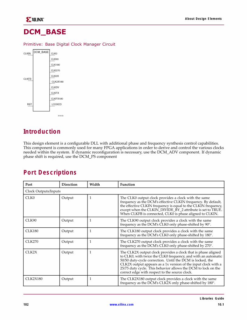
About Design Elements
DCM_BASE
Primitive: Base Digital Clock Manager Circuit
IntroductionThis design element is a configurable DLL with additional phase and frequency synthesis control capabilities.This component is commonly used for many FPGA applications in order to derive and control the various clocksneeded within the system. If dynamic reconfiguration is necessary, use the DCM_ADV component. If dynamicphase shift is required, use the DCM_PS component
Port DescriptionsPort Direction Width Function
Clock Outputs/Inputs
CLK0 Output 1 The CLK0 output clock provides a clock with the samefrequency as the DCM’s effective CLKIN frequency. By default,the effective CLKIN frequency is equal to the CLKIN frequency,except when the CLKIN_DIVIDE_BY_2 attribute is set to TRUE.When CLKFB is connected, CLK0 is phase aligned to CLKIN.
CLK90 Output 1 The CLK90 output clock provides a clock with the samefrequency as the DCM’s CLK0 only phase-shifted by 90°.
CLK180 Output 1 The CLK180 output clock provides a clock with the samefrequency as the DCM’s CLK0 only phase-shifted by 180°.
CLK270 Output 1 The CLK270 output clock provides a clock with the samefrequency as the DCM’s CLK0 only phase-shifted by 270°.
CLK2X Output 1 The CLK2X output clock provides a clock that is phase alignedto CLK0, with twice the CLK0 frequency, and with an automatic50/50 duty-cycle correction. Until the DCM is locked, theCLK2X output appears as a 1x version of the input clock with a25/75 duty cycle. This behavior allows the DCM to lock on thecorrect edge with respect to the source clock.
CLK2X180 Output 1 The CLK2X180 output clock provides a clock with the samefrequency as the DCM’s CLK2X only phase-shifted by 180°.
Libraries Guide
182 www.xilinx.com 10.1
About Design Elements
Port Direction Width Function
CLKDV Output 1 The frequency divide (CLKDV) output clock provides a clockthat is phase aligned to CLK0 with a frequency that is a fractionof the effective CLKIN frequency. The fraction is determined bythe CLKDV_DIVIDE attribute. By default, the effective CLKINfrequency is equal to the CLKIN frequency, except when theCLKIN_DIVIDE_BY_2 attribute is set to TRUE.
CLKFX Output 1 The frequency (CLKFX) output clock provides a clock with thefollowing frequency definition:
CLKFX Frequency = (M/D) x (Effective CLKIN Frequency)
In this equation, M is the multiplier (numerator) with a valuedefined by the CLKFX_MULTIPLY attribute. D is the divisor(denominator) with a value defined by the CLKFX_DIVIDEattribute. Specifications for M and D, as well as input andoutput frequency ranges for the frequency synthesizer, areprovided in the Data Sheet for this architecture. The rising edgeof CLKFX output is phase aligned to the rising edges of CLK0,CLK2X, and CLKDV when the feedback path (CLKFB) is used.When M and D to have no common factor, the alignment occursonly once every D cycles of CLK0. By default, the effectiveCLKIN frequency is equal to the CLKIN frequency, exceptwhen the CLKIN_DIVIDE_BY_2 attribute is set to TRUE.
CLKFX180 Output 1 The CLKFX180 output clock provides a clock with the samefrequency as the DCM’s CLKFX only phase-shifted by 180°.
CLKIN Input 1 The source clock (CLKIN) input pin provides the source clockto the DCM. The CLKIN frequency must fall in the rangesspecified in the Data Sheet for this architecture. The clock inputsignal comes from one of the following buffers:
1. IBUFG - Global Clock Input Buffer. The DCM compensatesfor the clock input path when an IBUFG on the same edge (topor bottom) of the device as the DCM is used.
2. BUFG/BUFGCTRL - Internal Global Clock Buffer. AnyBUFGCTRL can drive any DCM in the Virtex-5 device using thededicated global routing. A BUFGCTRL can drive the DCMCLKIN pin when used to connect two DCM in series.
3. IBUF - Input Buffer. When IBUF drives CLKIN input, thePAD to DCM input skew is not compensated and increased jittercan occur. This configuration is generally not recommended.
CLKFB Input 1 The feedback clock (CLKFB) input pin provides a referenceor feedback signal to the DCM to delay-compensate the clockoutputs, and align it with the clock input. To provide thenecessary feedback to the DCM, connect only the CLK0 outputto the CLKFB input via a BUFG component in the case ofinternal feedback or an OBUF ’ IBUFG to the case of externalfeedback. Set the CLK_FEEDBACK attribute to 1X. When theCLKFB pin is connected, CLK0, CLKDV, and CLKFX are phasealigned to CLKIN. When the CLKFB pin is not connected,set CLK_FEEDBACK to NONE and only the CLKFX andCLKFX180 outputs are valid however not phase aligned toCLKIN.
Status Outputs / Control Inputs
Libraries Guide
10.1 www.xilinx.com 183
About Design Elements
Port Direction Width Function
LOCKED Output 1 Synchronous output from the PLL that provides you with anindication the PLL has achieved phase alignment and is readyfor operation.
RST Input 1 The reset (RST) input pin resets the DCM circuitry. The RSTsignal is an active High asynchronous reset. Asserting theRST signal asynchronously forces all DCM outputs Low (theLOCKED signal, all status signals, and all output clocks withinfour source clock cycles). Because the reset is asynchronous,the last cycle of the clocks can exhibit an unintended shortpulse, severely distorted duty-cycle, and no longer phase adjustwith respect to one another while deasserting. The RST pinmust be used when reconfiguring the device or changing theinput frequency. Deasserting the RST signal synchronouslystarts the locking process at the next CLKIN cycle. To ensure aproper DCM reset and locking process, the RST signal must bedeasserted after the CLKIN signal has been present and stablefor at least three clock cycles. In all designs, the DCM must beheld in reset until the clock is stable. During configuration, theDCM is automatically held in reset until GSR is released. If theclock is stable when GSR is released.
Design Entry MethodThis design element can be used in schematics.
Available AttributesAttribute Type Allowed Values Default Description
CLK_FEEDBACK String "1X" , "2X", or "NONE” “1X” Specifies the feedback input tothe DCM (CLK0, or CLK2X).
CLKDV_DIVIDE Float 1.5, 2.0, 2.5, 3.0, 3.5, 4.0, 4.5,5.0, 5.5, 6.0, 6.5, 7.0, 7.5, 8.0,9.0, 10.0, 11.0, 12.0, 13.0,14.0, 15.0 or 16.0
2.0 Specifies the extent to whichthe CLKDLL, CLKDLLE,CLKDLLHF, or DCM clockdivider (CLKDV output) is to befrequency divided.
CLKFX_DIVIDE Integer 1 to 32 1 Specifies the frequency dividervalue for the CLKFX output.
CLKFX_MULTIPLY Integer 2 to 32 4 Specifies the frequencymultipliervalue for the CLKFX output.
CLKIN_DIVIDE_BY_2
Boolean FALSE, TRUE FALSE Allows for the input clockfrequency to be divided inhalf when such a reduction isnecessary to meet the DCM inputclock frequency requirements.
CLKIN_PERIOD Float 1.25 to 1000.00 0.0 Specifies the period of inputclock in ns from 1.25 to 1000.00.
CLKOUT_PHASE_SHIFT
String "NONE", "FIXED","VARIABLE_ POSITIVE","VARIABLE_ CENTER"or "DIRECT”
"NONE" Specifies the phase shift mode ofallowed value.
Libraries Guide
184 www.xilinx.com 10.1
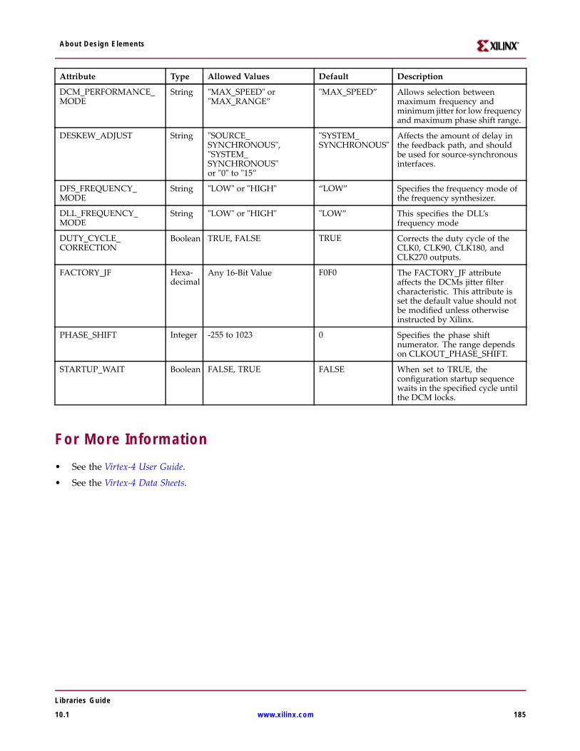
About Design Elements
Attribute Type Allowed Values Default Description
DCM_PERFORMANCE_MODE
String "MAX_SPEED" or"MAX_RANGE”
"MAX_SPEED” Allows selection betweenmaximum frequency andminimum jitter for low frequencyand maximum phase shift range.
DESKEW_ADJUST String "SOURCE_SYNCHRONOUS","SYSTEM_SYNCHRONOUS"or "0" to "15”
"SYSTEM_SYNCHRONOUS"
Affects the amount of delay inthe feedback path, and shouldbe used for source-synchronousinterfaces.
DFS_FREQUENCY_MODE
String "LOW" or "HIGH" “LOW” Specifies the frequency mode ofthe frequency synthesizer.
DLL_FREQUENCY_MODE
String "LOW" or "HIGH" "LOW” This specifies the DLL’sfrequency mode
DUTY_CYCLE_CORRECTION
Boolean TRUE, FALSE TRUE Corrects the duty cycle of theCLK0, CLK90, CLK180, andCLK270 outputs.
FACTORY_JF Hexa-decimal
Any 16-Bit Value F0F0 The FACTORY_JF attributeaffects the DCMs jitter filtercharacteristic. This attribute isset the default value should notbe modified unless otherwiseinstructed by Xilinx.
PHASE_SHIFT Integer -255 to 1023 0 Specifies the phase shiftnumerator. The range dependson CLKOUT_PHASE_SHIFT.
STARTUP_WAIT Boolean FALSE, TRUE FALSE When set to TRUE, theconfiguration startup sequencewaits in the specified cycle untilthe DCM locks.
For More Information• See the Virtex-4 User Guide.
• See the Virtex-4 Data Sheets.
Libraries Guide
10.1 www.xilinx.com 185
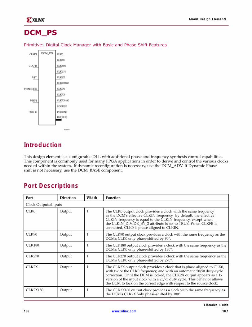
About Design Elements
DCM_PS
Primitive: Digital Clock Manager with Basic and Phase Shift Features
IntroductionThis design element is a configurable DLL with additional phase and frequency synthesis control capabilities.This component is commonly used for many FPGA applications in order to derive and control the various clocksneeded within the system. If dynamic reconfiguration is necessary, use the DCM_ADV. If Dynamic Phaseshift is not necessary, use the DCM_BASE component.
Port DescriptionsPort Direction Width Function
Clock Outputs/Inputs
CLK0 Output 1 The CLK0 output clock provides a clock with the same frequencyas the DCM’s effective CLKIN frequency. By default, the effectiveCLKIN frequency is equal to the CLKIN frequency, except whenthe CLKIN_DIVIDE_BY_2 attribute is set to TRUE. When CLKFB isconnected, CLK0 is phase aligned to CLKIN.
CLK90 Output 1 The CLK90 output clock provides a clock with the same frequency as theDCM’s CLK0 only phase-shifted by 90°.
CLK180 Output 1 The CLK180 output clock provides a clock with the same frequency as theDCM’s CLK0 only phase-shifted by 180°.
CLK270 Output 1 The CLK270 output clock provides a clock with the same frequency as theDCM’s CLK0 only phase-shifted by 270°.
CLK2X Output 1 The CLK2X output clock provides a clock that is phase aligned to CLK0,with twice the CLK0 frequency, and with an automatic 50/50 duty-cyclecorrection. Until the DCM is locked, the CLK2X output appears as a 1xversion of the input clock with a 25/75 duty cycle. This behavior allowsthe DCM to lock on the correct edge with respect to the source clock.
CLK2X180 Output 1 The CLK2X180 output clock provides a clock with the same frequency asthe DCM’s CLK2X only phase-shifted by 180°.
Libraries Guide
186 www.xilinx.com 10.1
About Design Elements
Port Direction Width Function
CLKDV Output 1 The frequency divide (CLKDV) output clock provides a clock that isphase aligned to CLK0 with a frequency that is a fraction of the effectiveCLKIN frequency. The fraction is determined by the CLKDV_DIVIDEattribute. By default, the effective CLKIN frequency is equal to the CLKINfrequency, except when the CLKIN_DIVIDE_BY_2 attribute is set to TRUE.
CLKFX Output 1 The frequency (CLKFX) output clock provides a clock with the followingfrequency definition:
CLKFX Frequency = (M/D) x (Effective CLKIN Frequency)
In this equation, M is the multiplier (numerator) with a value defined bythe CLKFX_MULTIPLY attribute. D is the divisor (denominator) witha value defined by the CLKFX_DIVIDE attribute. Specifications for Mand D, as well as input and output frequency ranges for the frequencysynthesizer, are provided in the Virtex-5 Data Sheet. The rising edge ofCLKFX output is phase aligned to the rising edges of CLK0, CLK2X,and CLKDV when the feedback path (CLKFB) is used. When M andD to have no common factor, the alignment occurs only once every Dcycles of CLK0. By default, the effective CLKIN frequency is equal tothe CLKIN frequency, except when the CLKIN_DIVIDE_BY_2 attributeis set to TRUE.
CLKFX180 Output 1 The CLKFX180 output clock provides a clock with the same frequency asthe DCM’s CLKFX only phase-shifted by 180°.
CLKIN Input 1 The source clock (CLKIN) input pin provides the source clock to the DCM.The CLKIN frequency must fall in the ranges specified in the Virtex-5 DataSheet. The clock input signal comes from one of the following buffers:
1. IBUFG - Global Clock Input Buffer. The DCM compensates for theclock input path when an IBUFG on the same edge (top or bottom) of thedevice as the DCM is used.
2. BUFG/BUFGCTRL - Internal Global Clock Buffer. Any BUFGCTRL candrive any DCM in the Virtex-5 device using the dedicated global routing.A BUFGCTRL can drive the DCM CLKIN pin when used to connect twoDCM in series.
3. IBUF - Input Buffer. When IBUF drives CLKIN input, the PAD toDCM input skew is not compensated and increased jitter can occur. Thisconfiguration is generally not recommended.
CLKFB Input 1 The feedback clock (CLKFB) input pin provides a reference or feedbacksignal to the DCM to delay-compensate the clock outputs, and align itwith the clock input. To provide the necessary feedback to the DCM,connect only the CLK0 output to the CLKFB input via a BUFG componentin the case of internal feedback or an OBUF ’ IBUFG to the case of externalfeedback. Set the CLK_FEEDBACK attribute to 1X. When the CLKFB pinis connected, CLK0, CLKDV, and CLKFX are phase aligned to CLKIN.When the CLKFB pin is not connected, set CLK_FEEDBACK to NONEand only the CLKFX and CLKFX180 outputs are valid however not phasealigned to CLKIN.
Status Outputs / Control Inputs
LOCKED Output 1 Synchronous output from the PLL that provides you with an indicationthe PLL has achieved phase alignment and is ready for operation.
PSDONE Output 1 Dynamic CLKIN select input. When high, ’1’ CLKIN1 is selected andwhile low, ’0’ CLKIN2 is selected. If dual clock selection is not necessary,connect this input to a logic 1.
Libraries Guide
10.1 www.xilinx.com 187
About Design Elements
Port Direction Width Function
RST Input 1 The reset (RST) input pin resets the DCM circuitry. The RST signal is anactive High asynchronous reset. Asserting the RST signal asynchronouslyforces all DCM outputs Low (the LOCKED signal, all status signals, andall output clocks within four source clock cycles). Because the reset isasynchronous, the last cycle of the clocks can exhibit an unintended shortpulse, severely distorted duty-cycle, and no longer phase adjust withrespect to one another while deasserting. The RST pin must be used whenreconfiguring the device or changing the input frequency. Deasserting theRST signal synchronously starts the locking process at the next CLKINcycle. To ensure a proper DCM reset and locking process, the RST signalmust be deasserted after the CLKIN signal has been present and stable forat least three clock cycles. In all designs, the DCM must be held in resetuntil the clock is stable. During configuration, the DCM is automaticallyheld in reset until GSR is released. If the clock is stable when GSR is releas
PSCLK Input 1 The phase-shift clock (PSCLK) input pin provides the source clock forthe DCM phase shift. The phase-shift clock signal can be driven by anyclock source (external or internal).
The frequency range of PSCLK is defined by PSCLK_FREQ_LF/HF (seethe Virtex-5 Data Sheet). This input must be tied to ground when theCLKOUT_PHASE_SHIFT attribute is set to NONE or FIXED.
PSINCDEC Input 1 The PSINCDEC input signal is synchronous with PSCLK. The PSINCDECinput signal is used to increment or decrement the phase-shift factorwhen CLKOUT_PHASE_SHIFT is set to one of the variable modes. As aresult, the output clock is phase shifted. the PSINCDEC signal is assertedHigh for increment, or deasserted Low for decrement. This input mustbe tied to ground when the CLKOUT_PHASE_SHIFT attribute is set toNONE or FIXED.
PSEN Input 1 The PSEN input signal is synchronous with PSCLK. A variablephase-shift operation is initiated by the PSEN input signal whenCLKOUT_PHASE_SHIFT is set to a variable mode. It must be activatedfor one period of PSCLK. After PSEN is initiated, the phase change iseffective for up to 100 CLKIN pulse cycles, plus three PSCLK cycles, and isindicated by a High pulse on PSDONE. There are no sporadic changes orglitches on any output during the phase transition. From the time PSEN isenabled until PSDONE is flagged, the DCM output clock moves bit-by-bitfrom its original phase shift to the target phase shift. The phase-shift iscomplete when PSDONE is flagged. PSEN must be tied to ground whenthe CLKOUT_PHASE_SHIFT attribute is set to NONE or FIXED.
Design Entry MethodThis design element can be used in schematics.
Available AttributesAttribute Type Allowed Values Default Description
CLK_FEEDBACK String "1X", "2X",or "NONE”
"1X” Specifies the clock feedback ofallowed value.
CLKDV_DIVIDE FLOAT 1.5, 2.0, 2.5, 3.0, 3.5,4.0, 4.5, 5.0, 5.5, 6.0,6.5, 7.0, 7.5, 8.0, 9.0,10.0, 11.0, 12.0, 13.0,14.0, 15.0 or 16.0
2.0 Specifies the extent to which theCLKDLL, CLKDLLE, CLKDLLHF,or DCM clock divider (CLKDVoutput) is to be frequency divided.
Libraries Guide
188 www.xilinx.com 10.1
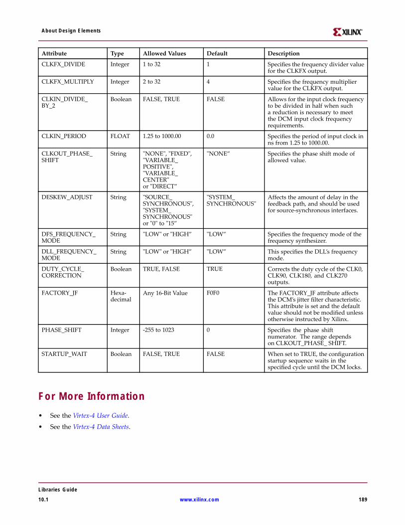
About Design Elements
Attribute Type Allowed Values Default Description
CLKFX_DIVIDE Integer 1 to 32 1 Specifies the frequency divider valuefor the CLKFX output.
CLKFX_MULTIPLY Integer 2 to 32 4 Specifies the frequency multipliervalue for the CLKFX output.
CLKIN_DIVIDE_BY_2
Boolean FALSE, TRUE FALSE Allows for the input clock frequencyto be divided in half when sucha reduction is necessary to meetthe DCM input clock frequencyrequirements.
CLKIN_PERIOD FLOAT 1.25 to 1000.00 0.0 Specifies the period of input clock inns from 1.25 to 1000.00.
CLKOUT_PHASE_SHIFT
String "NONE", "FIXED","VARIABLE_POSITIVE","VARIABLE_CENTER"or "DIRECT”
"NONE” Specifies the phase shift mode ofallowed value.
DESKEW_ADJUST String "SOURCE_SYNCHRONOUS","SYSTEM_SYNCHRONOUS"or "0" to "15”
"SYSTEM_SYNCHRONOUS"
Affects the amount of delay in thefeedback path, and should be usedfor source-synchronous interfaces.
DFS_FREQUENCY_MODE
String "LOW" or "HIGH” "LOW” Specifies the frequency mode of thefrequency synthesizer.
DLL_FREQUENCY_MODE
String "LOW" or "HIGH” "LOW” This specifies the DLL’s frequencymode.
DUTY_CYCLE_CORRECTION
Boolean TRUE, FALSE TRUE Corrects the duty cycle of the CLK0,CLK90, CLK180, and CLK270outputs.
FACTORY_JF Hexa-decimal
Any 16-Bit Value F0F0 The FACTORY_JF attribute affectsthe DCM’s jitter filter characteristic.This attribute is set and the defaultvalue should not be modified unlessotherwise instructed by Xilinx.
PHASE_SHIFT Integer -255 to 1023 0 Specifies the phase shiftnumerator. The range dependson CLKOUT_PHASE_ SHIFT.
STARTUP_WAIT Boolean FALSE, TRUE FALSE When set to TRUE, the configurationstartup sequence waits in thespecified cycle until the DCM locks.
For More Information• See the Virtex-4 User Guide.
• See the Virtex-4 Data Sheets.
Libraries Guide
10.1 www.xilinx.com 189
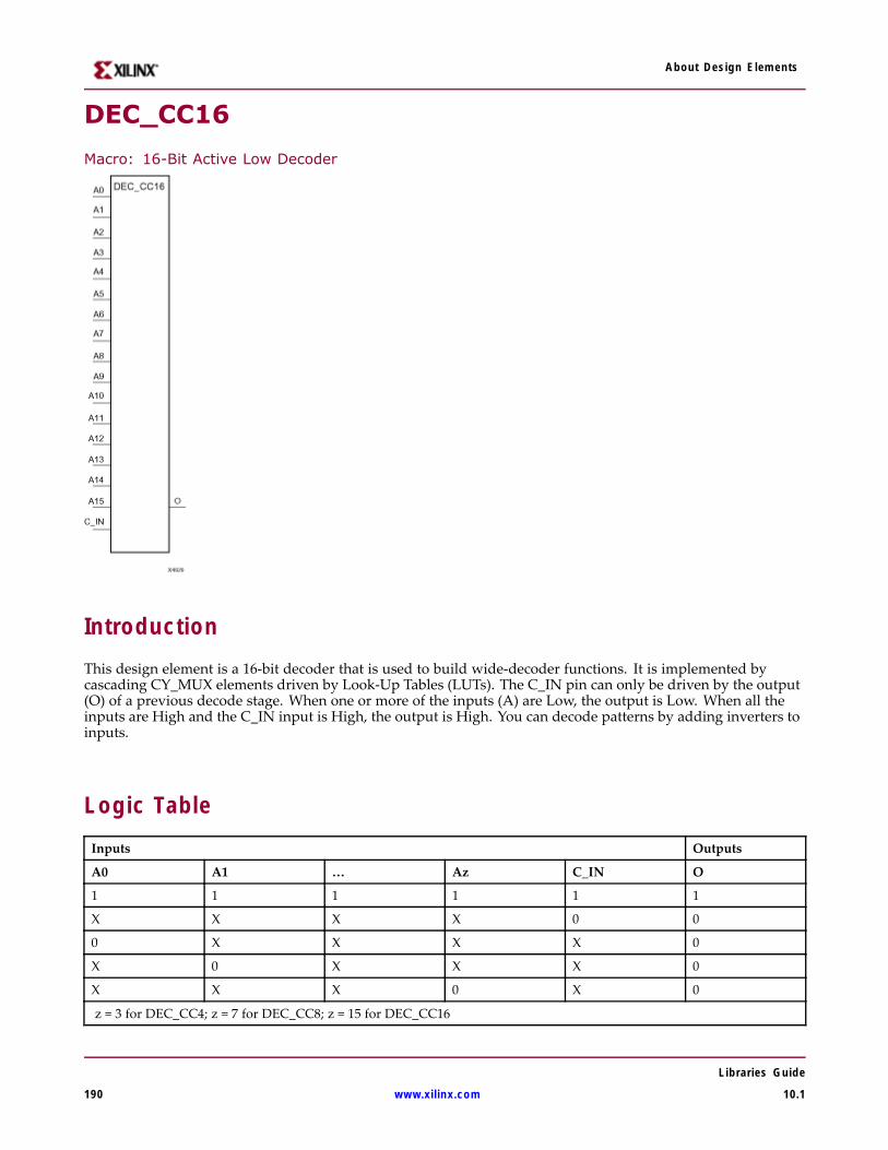
About Design Elements
DEC_CC16
Macro: 16-Bit Active Low Decoder
IntroductionThis design element is a 16-bit decoder that is used to build wide-decoder functions. It is implemented bycascading CY_MUX elements driven by Look-Up Tables (LUTs). The C_IN pin can only be driven by the output(O) of a previous decode stage. When one or more of the inputs (A) are Low, the output is Low. When all theinputs are High and the C_IN input is High, the output is High. You can decode patterns by adding inverters toinputs.
Logic TableInputs Outputs
A0 A1 … Az C_IN O
1 1 1 1 1 1
X X X X 0 0
0 X X X X 0
X 0 X X X 0
X X X 0 X 0
z = 3 for DEC_CC4; z = 7 for DEC_CC8; z = 15 for DEC_CC16
Libraries Guide
190 www.xilinx.com 10.1

About Design Elements
Design Entry MethodThis design element is only for use in schematics.
For More Information• See the Virtex-4 User Guide.
• See the Virtex-4 Data Sheets.
Libraries Guide
10.1 www.xilinx.com 191
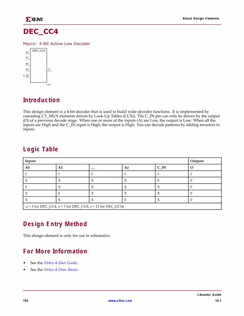
About Design Elements
DEC_CC4
Macro: 4-Bit Active Low Decoder
IntroductionThis design element is a 4-bit decoder that is used to build wide-decoder functions. It is implemented bycascading CY_MUX elements driven by Look-Up Tables (LUTs). The C_IN pin can only be driven by the output(O) of a previous decode stage. When one or more of the inputs (A) are Low, the output is Low. When all theinputs are High and the C_IN input is High, the output is High. You can decode patterns by adding inverters toinputs.
Logic TableInputs Outputs
A0 A1 … Az C_IN O
1 1 1 1 1 1
X X X X 0 0
0 X X X X 0
X 0 X X X 0
X X X 0 X 0
z = 3 for DEC_CC4; z = 7 for DEC_CC8; z = 15 for DEC_CC16
Design Entry MethodThis design element is only for use in schematics.
For More Information• See the Virtex-4 User Guide.
• See the Virtex-4 Data Sheets.
Libraries Guide
192 www.xilinx.com 10.1
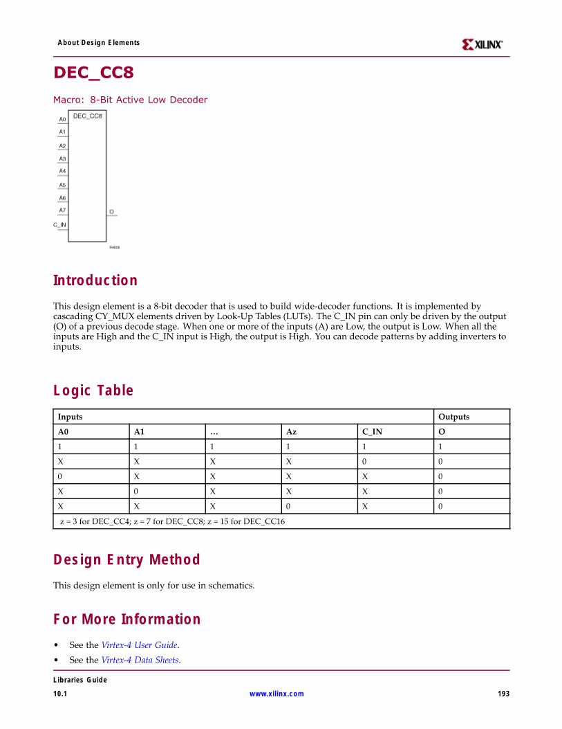
About Design Elements
DEC_CC8
Macro: 8-Bit Active Low Decoder
IntroductionThis design element is a 8-bit decoder that is used to build wide-decoder functions. It is implemented bycascading CY_MUX elements driven by Look-Up Tables (LUTs). The C_IN pin can only be driven by the output(O) of a previous decode stage. When one or more of the inputs (A) are Low, the output is Low. When all theinputs are High and the C_IN input is High, the output is High. You can decode patterns by adding inverters toinputs.
Logic TableInputs Outputs
A0 A1 … Az C_IN O
1 1 1 1 1 1
X X X X 0 0
0 X X X X 0
X 0 X X X 0
X X X 0 X 0
z = 3 for DEC_CC4; z = 7 for DEC_CC8; z = 15 for DEC_CC16
Design Entry MethodThis design element is only for use in schematics.
For More Information• See the Virtex-4 User Guide.• See the Virtex-4 Data Sheets.
Libraries Guide
10.1 www.xilinx.com 193
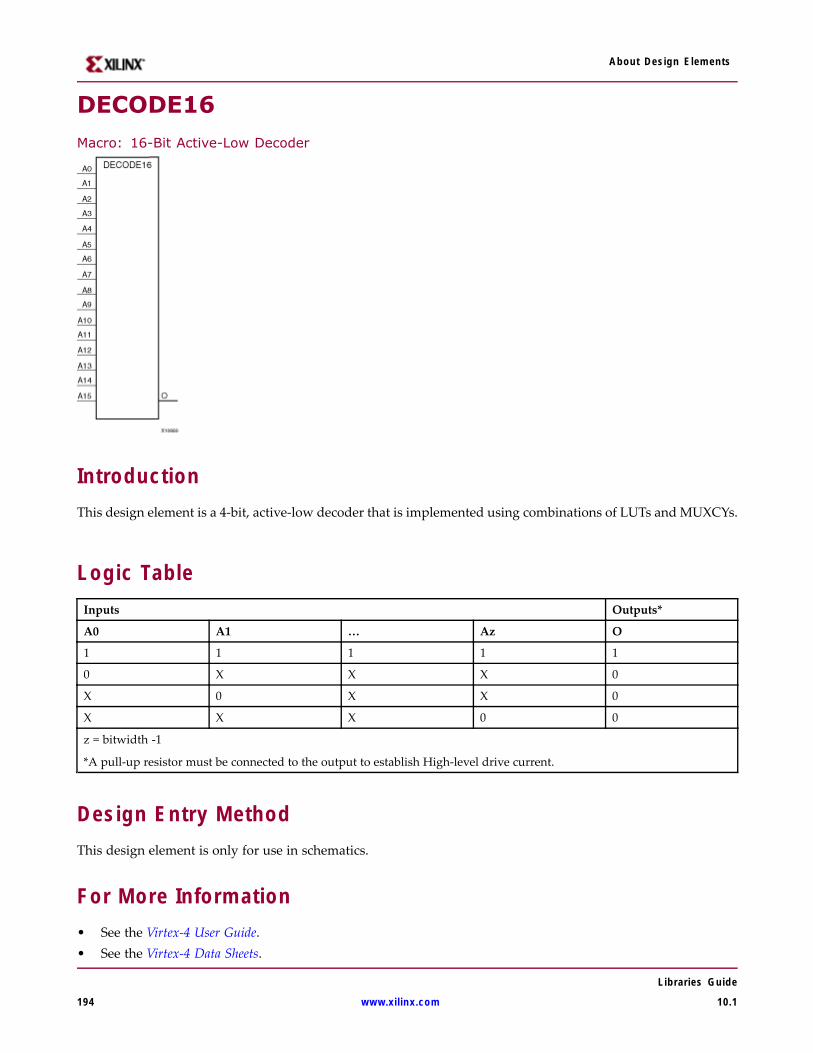
About Design Elements
DECODE16
Macro: 16-Bit Active-Low Decoder
IntroductionThis design element is a 4-bit, active-low decoder that is implemented using combinations of LUTs and MUXCYs.
Logic TableInputs Outputs*
A0 A1 … Az O
1 1 1 1 1
0 X X X 0
X 0 X X 0
X X X 0 0
z = bitwidth -1
*A pull-up resistor must be connected to the output to establish High-level drive current.
Design Entry MethodThis design element is only for use in schematics.
For More Information• See the Virtex-4 User Guide.• See the Virtex-4 Data Sheets.
Libraries Guide
194 www.xilinx.com 10.1
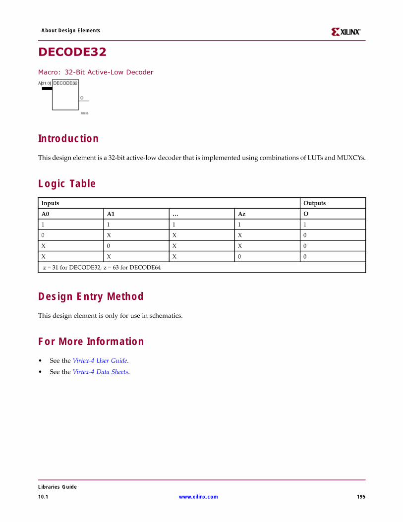
About Design Elements
DECODE32
Macro: 32-Bit Active-Low Decoder
IntroductionThis design element is a 32-bit active-low decoder that is implemented using combinations of LUTs andMUXCYs.
Logic TableInputs Outputs
A0 A1 … Az O
1 1 1 1 1
0 X X X 0
X 0 X X 0
X X X 0 0
z = 31 for DECODE32, z = 63 for DECODE64
Design Entry MethodThis design element is only for use in schematics.
For More Information• See the Virtex-4 User Guide.
• See the Virtex-4 Data Sheets.
Libraries Guide
10.1 www.xilinx.com 195
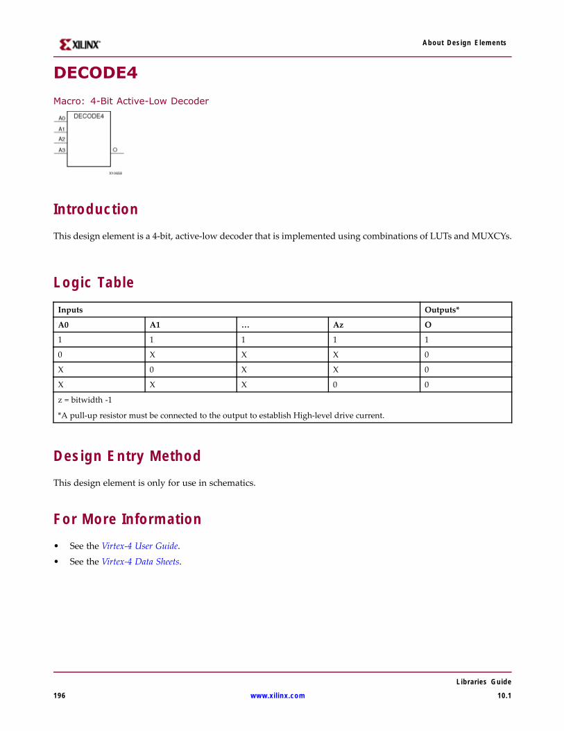
About Design Elements
DECODE4
Macro: 4-Bit Active-Low Decoder
IntroductionThis design element is a 4-bit, active-low decoder that is implemented using combinations of LUTs and MUXCYs.
Logic TableInputs Outputs*
A0 A1 … Az O
1 1 1 1 1
0 X X X 0
X 0 X X 0
X X X 0 0
z = bitwidth -1
*A pull-up resistor must be connected to the output to establish High-level drive current.
Design Entry MethodThis design element is only for use in schematics.
For More Information• See the Virtex-4 User Guide.
• See the Virtex-4 Data Sheets.
Libraries Guide
196 www.xilinx.com 10.1
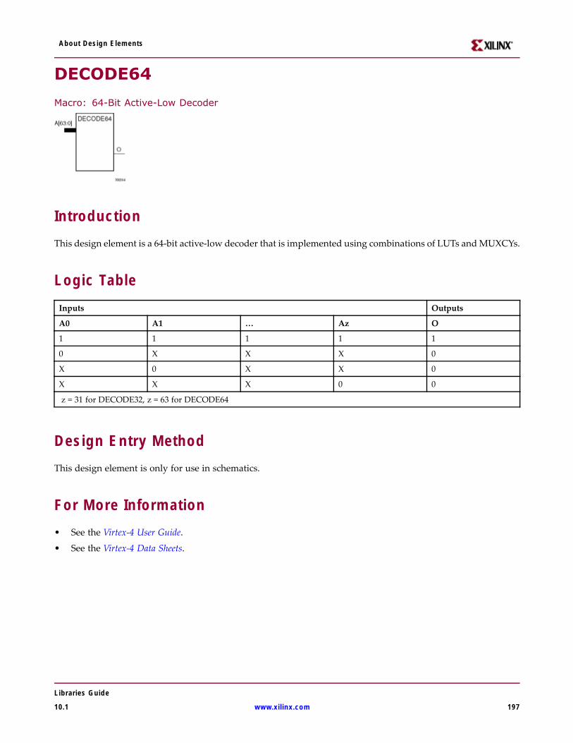
About Design Elements
DECODE64
Macro: 64-Bit Active-Low Decoder
IntroductionThis design element is a 64-bit active-low decoder that is implemented using combinations of LUTs andMUXCYs.
Logic TableInputs Outputs
A0 A1 … Az O
1 1 1 1 1
0 X X X 0
X 0 X X 0
X X X 0 0
z = 31 for DECODE32, z = 63 for DECODE64
Design Entry MethodThis design element is only for use in schematics.
For More Information• See the Virtex-4 User Guide.
• See the Virtex-4 Data Sheets.
Libraries Guide
10.1 www.xilinx.com 197
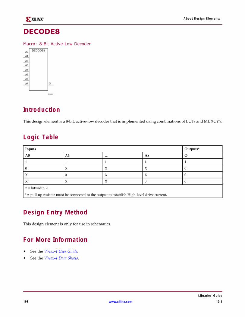
About Design Elements
DECODE8
Macro: 8-Bit Active-Low Decoder
IntroductionThis design element is a 8-bit, active-low decoder that is implemented using combinations of LUTs andMUXCY’s.
Logic TableInputs Outputs*
A0 A1 … Az O
1 1 1 1 1
0 X X X 0
X 0 X X 0
X X X 0 0
z = bitwidth -1
*A pull-up resistor must be connected to the output to establish High-level drive current.
Design Entry MethodThis design element is only for use in schematics.
For More Information• See the Virtex-4 User Guide.
• See the Virtex-4 Data Sheets.
Libraries Guide
198 www.xilinx.com 10.1
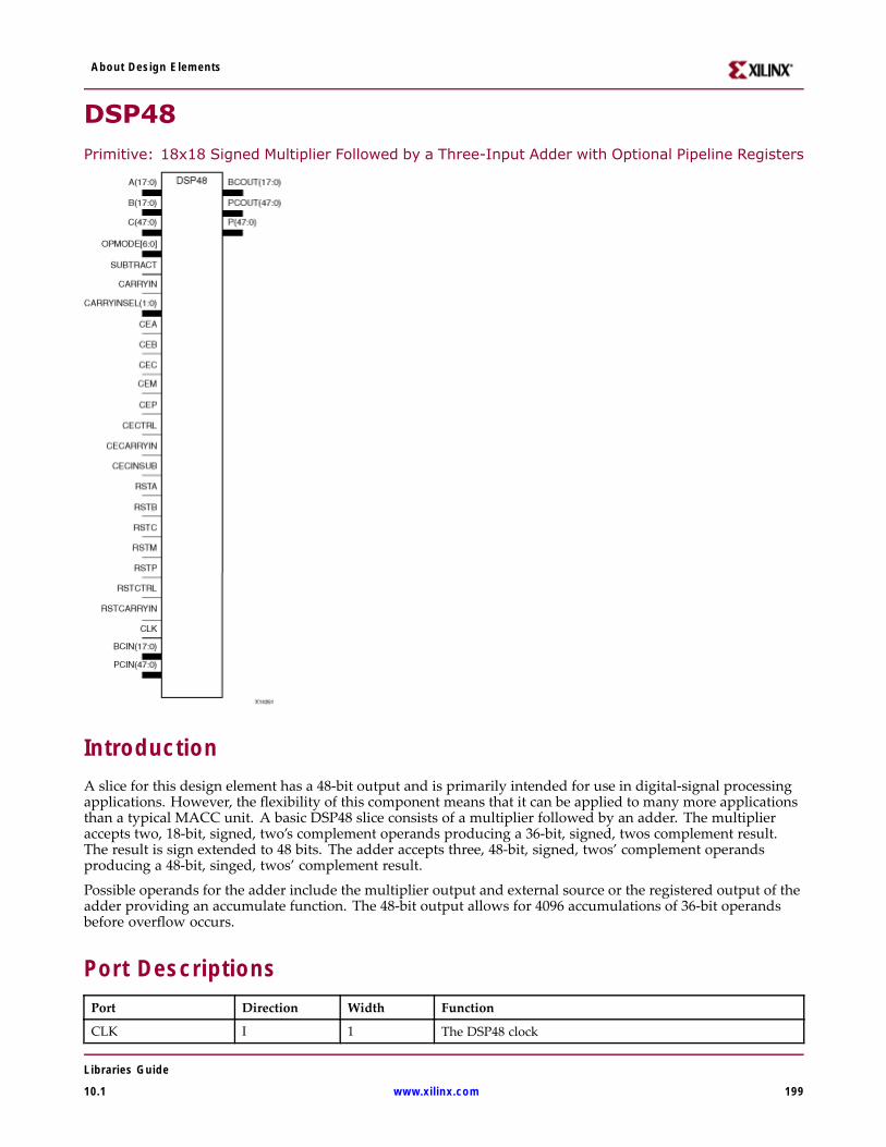
About Design Elements
DSP48Primitive: 18x18 Signed Multiplier Followed by a Three-Input Adder with Optional Pipeline Registers
IntroductionA slice for this design element has a 48-bit output and is primarily intended for use in digital-signal processingapplications. However, the flexibility of this component means that it can be applied to many more applicationsthan a typical MACC unit. A basic DSP48 slice consists of a multiplier followed by an adder. The multiplieraccepts two, 18-bit, signed, two’s complement operands producing a 36-bit, signed, twos complement result.The result is sign extended to 48 bits. The adder accepts three, 48-bit, signed, twos’ complement operandsproducing a 48-bit, singed, twos’ complement result.
Possible operands for the adder include the multiplier output and external source or the registered output of theadder providing an accumulate function. The 48-bit output allows for 4096 accumulations of 36-bit operandsbefore overflow occurs.
Port DescriptionsPort Direction Width Function
CLK I 1 The DSP48 clock
Libraries Guide
10.1 www.xilinx.com 199
About Design Elements
Port Direction Width Function
A I 18 The multiplier’s A input, can also be used as adder’s MSWinput
B I 18 The multiplier’s B input, can also be used as adder’s LSWinput
BCIN I 18 The multiplier’s cascaded B input, can also be used as adder’sLSW input
C I 48 The adder’s C input
PCIN I 48 Cascaded adder’s C Input from previous DSP slice
CARRYIN I 1 The adders carry input
SUBTRACT I 1 0= add, 1= (C, PCIN)-(mult,A:B)
OPMODE I 7 Controls input to adder in DSP48 slices- see OPMODE table
CARRYINSEL I 2 Selects carry source - see CARRINSEL table
CEA I 1 Clock enable - 0=hold 1=enable AREG
CEB I 1 Clock enable - 0=hold 1=enable BREG
CEC I 1 Clock enable - 0=hold 1=enable CREG
CEP I 1 Clock enable - 0=hold 1=enable PREG
Synthesis Attributes Used to Define Pipeline Registers
The following table describes the synthesis attributes used to define the pipeline registers.
Attribute Function
AREG 0=bypass, 1=single, 2=dual
BREG 0=bypass, 1=single, 2=dual
CREG 0=bypass, 1=single
PREG 0=bypass, 1=single
MREG 0=bypass, 1=single
SUBTRACTREG 0=bypass, 1=single
OPMODEREG 0=bypass, 1=single
CARRYINSELREG 0=bypass, 1=single
Twos Complement Signed Multiplier
The multiplier inside the DSP48 slice is an 18-bit x 18-bit twos complement multiplier with a 36-bit signed twoscomplement result. Cascading of multipliers to achieve larger products is supported. Applications such assigned-signed, signed-unsigned, and unsigned-unsigned multiplication, logical, arithmetic, barrel-shifter, twoscomplement and magnitude return are easily implemented. There are two independent dynamic data inputports. The input ports can represent 18-bit signed or 17-bit unsigned data.
X, Y, and Z Multiplexers
The Operational Mode (OpMode) inputs provide a way for the design to change its functionality on the fly. Forexample, the loading of an accumulator to restart an accumulation process. The OpMode bits can be optionallyregistered under the control of the configuration RAM.
The following tables list the possible values of OpMode and resulting function at the outputs of the threemultiplexers supplying data to the adder/subtracter. The 7-bit OpMode control can be further broken down intomultiplexer select bits. Not all possible combinations for the multiplexer select bits are allowed. If the multiplieroutput is selected then both the X and Y multiplexer are consumed with the multiplier output.
OpMode Control Bit Select X, Y, and Z Multiplexer Outputs
Libraries Guide
200 www.xilinx.com 10.1
About Design Elements
OPMODE Binary X Multiplexer Output Fed to Add/Subtract
Z Y X
XXX XX 0 ZERO (Default)
XXX 1 1 Multiplier Output
XXX XX 10 P
XXX XX 11 A concatenated B
OpMode Control Bit Select X, Y, and Z Multiplexer Outputs
OPMODE Binary Y Multiplexer Output Fed to Add/Subtract
Z Y X
XXX 0 XX ZERO (Default)
XXX 1 1 Multiplier Output
XXX 10 XX Illegal selection
XXX 11 XX C
OpMode Controls X, Y, and Z Multiplexer Outputs
OPMODE Binary Y Multiplexer Output Fed to Add/Subtract
Z Y X
XXX 0 XX ZERO (Default)
XXX 1 1 Multiplier Output
XXX 10 XX Illegal selection
XXX 11 XX C
Three Input Adder/Subtracter Control Logic
The adder/subtracter output is a function of control and data inputs. The OpMode, as shown in the previoussection, selects the inputs to the X, Y, Z multiplexer that are directed to the three adder/subtracter inputs. It alsodescribed that when the multiplier output is selected, both X and Y multiplexers are occupied. With the inputs tothe adder/subtracter specified the function of the adder/subtracter itself must be examined. As with the inputmultiplexers, the OpMode bits specify a portion of this function. The table below shows this function. Thesymbol ± in the table means either add or subtract and is specified by the state of the subtract control.
Hex OpMode Binary OpMode Output of Adder/Subtracter Operation Description
[6:0] Z Y X
0x00 000 00 00 ±CIN Zero
0x02 000 00 10 ±(P + CIN) Hold P
0x03 000 00 11 ±(A:B + CIN) A:B select
0x05 000 01 01 ± (A ×B+CIN) Multiply
0x0c 000 11 00 ± (C + CIN) C select
0x0e 000 11 10 ± (C + P + CIN) Feedback add
0x0f 000 11 11 ± (A:B +C +CIN) 36-bit adder
0x10 001 00 00 PCIN ± CIN P cascade select
0x12 001 00 10 PCIN ± (P + CIN) P cascade feedback add
0x13 001 00 11 PCIN ±(A:B+CIN) P cascade add
Libraries Guide
10.1 www.xilinx.com 201
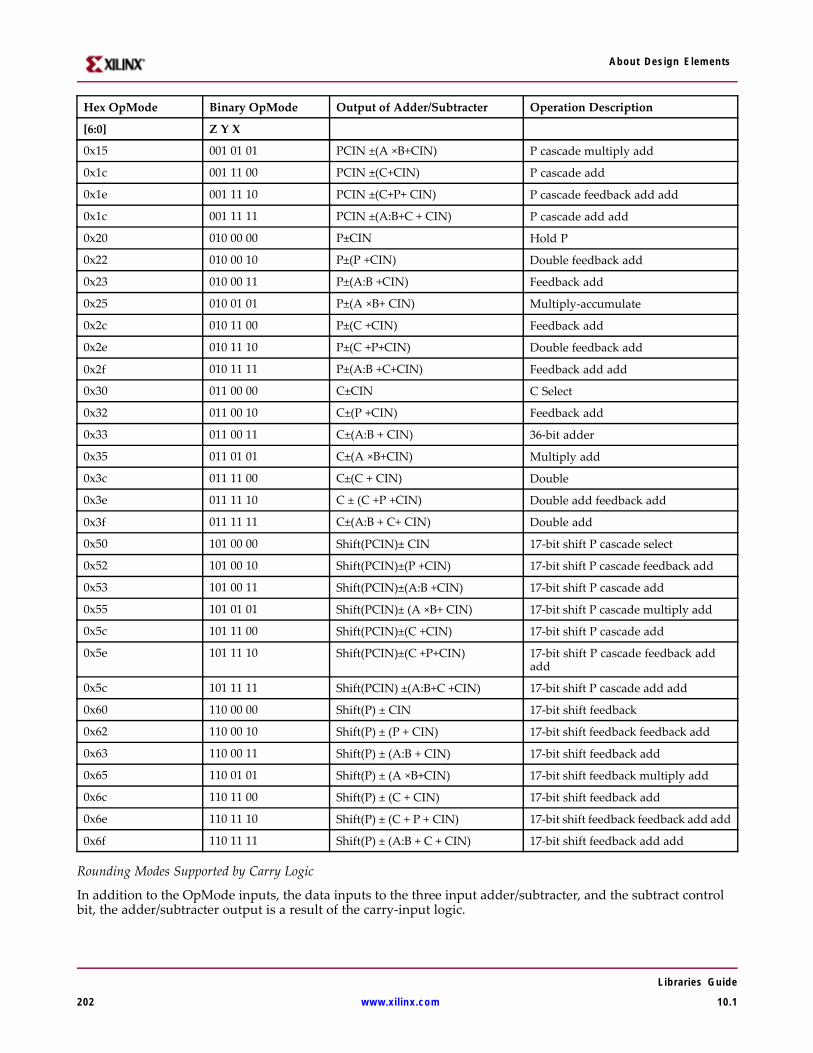
About Design Elements
Hex OpMode Binary OpMode Output of Adder/Subtracter Operation Description
[6:0] Z Y X
0x15 001 01 01 PCIN ±(A ×B+CIN) P cascade multiply add
0x1c 001 11 00 PCIN ±(C+CIN) P cascade add
0x1e 001 11 10 PCIN ±(C+P+ CIN) P cascade feedback add add
0x1c 001 11 11 PCIN ±(A:B+C + CIN) P cascade add add
0x20 010 00 00 P±CIN Hold P
0x22 010 00 10 P±(P +CIN) Double feedback add
0x23 010 00 11 P±(A:B +CIN) Feedback add
0x25 010 01 01 P±(A ×B+ CIN) Multiply-accumulate
0x2c 010 11 00 P±(C +CIN) Feedback add
0x2e 010 11 10 P±(C +P+CIN) Double feedback add
0x2f 010 11 11 P±(A:B +C+CIN) Feedback add add
0x30 011 00 00 C±CIN C Select
0x32 011 00 10 C±(P +CIN) Feedback add
0x33 011 00 11 C±(A:B + CIN) 36-bit adder
0x35 011 01 01 C±(A ×B+CIN) Multiply add
0x3c 011 11 00 C±(C + CIN) Double
0x3e 011 11 10 C ± (C +P +CIN) Double add feedback add
0x3f 011 11 11 C±(A:B + C+ CIN) Double add
0x50 101 00 00 Shift(PCIN)± CIN 17-bit shift P cascade select
0x52 101 00 10 Shift(PCIN)±(P +CIN) 17-bit shift P cascade feedback add
0x53 101 00 11 Shift(PCIN)±(A:B +CIN) 17-bit shift P cascade add
0x55 101 01 01 Shift(PCIN)± (A ×B+ CIN) 17-bit shift P cascade multiply add
0x5c 101 11 00 Shift(PCIN)±(C +CIN) 17-bit shift P cascade add
0x5e 101 11 10 Shift(PCIN)±(C +P+CIN) 17-bit shift P cascade feedback addadd
0x5c 101 11 11 Shift(PCIN) ±(A:B+C +CIN) 17-bit shift P cascade add add
0x60 110 00 00 Shift(P) ± CIN 17-bit shift feedback
0x62 110 00 10 Shift(P) ± (P + CIN) 17-bit shift feedback feedback add
0x63 110 00 11 Shift(P) ± (A:B + CIN) 17-bit shift feedback add
0x65 110 01 01 Shift(P) ± (A ×B+CIN) 17-bit shift feedback multiply add
0x6c 110 11 00 Shift(P) ± (C + CIN) 17-bit shift feedback add
0x6e 110 11 10 Shift(P) ± (C + P + CIN) 17-bit shift feedback feedback add add
0x6f 110 11 11 Shift(P) ± (A:B + C + CIN) 17-bit shift feedback add add
Rounding Modes Supported by Carry Logic
In addition to the OpMode inputs, the data inputs to the three input adder/subtracter, and the subtract controlbit, the adder/subtracter output is a result of the carry-input logic.
Libraries Guide
202 www.xilinx.com 10.1
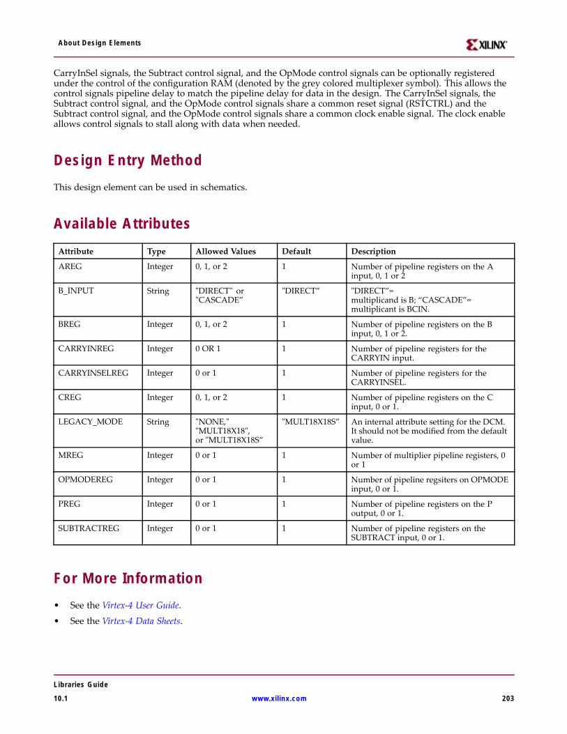
About Design Elements
CarryInSel signals, the Subtract control signal, and the OpMode control signals can be optionally registeredunder the control of the configuration RAM (denoted by the grey colored multiplexer symbol). This allows thecontrol signals pipeline delay to match the pipeline delay for data in the design. The CarryInSel signals, theSubtract control signal, and the OpMode control signals share a common reset signal (RSTCTRL) and theSubtract control signal, and the OpMode control signals share a common clock enable signal. The clock enableallows control signals to stall along with data when needed.
Design Entry MethodThis design element can be used in schematics.
Available AttributesAttribute Type Allowed Values Default Description
AREG Integer 0, 1, or 2 1 Number of pipeline registers on the Ainput, 0, 1 or 2
B_INPUT String "DIRECT" or"CASCADE”
"DIRECT” "DIRECT”=multiplicand is B; “CASCADE”=multiplicant is BCIN.
BREG Integer 0, 1, or 2 1 Number of pipeline registers on the Binput, 0, 1 or 2.
CARRYINREG Integer 0 OR 1 1 Number of pipeline registers for theCARRYIN input.
CARRYINSELREG Integer 0 or 1 1 Number of pipeline registers for theCARRYINSEL.
CREG Integer 0, 1, or 2 1 Number of pipeline registers on the Cinput, 0 or 1.
LEGACY_MODE String "NONE,""MULT18X18",or "MULT18X18S”
"MULT18X18S” An internal attribute setting for the DCM.It should not be modified from the defaultvalue.
MREG Integer 0 or 1 1 Number of multiplier pipeline registers, 0or 1
OPMODEREG Integer 0 or 1 1 Number of pipeline regsiters on OPMODEinput, 0 or 1.
PREG Integer 0 or 1 1 Number of pipeline registers on the Poutput, 0 or 1.
SUBTRACTREG Integer 0 or 1 1 Number of pipeline registers on theSUBTRACT input, 0 or 1.
For More Information• See the Virtex-4 User Guide.
• See the Virtex-4 Data Sheets.
Libraries Guide
10.1 www.xilinx.com 203
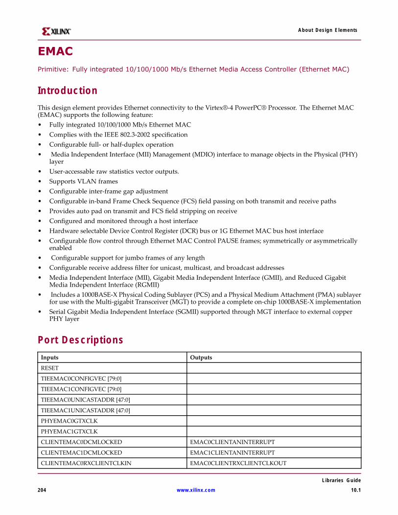
About Design Elements
EMACPrimitive: Fully integrated 10/100/1000 Mb/s Ethernet Media Access Controller (Ethernet MAC)
IntroductionThis design element provides Ethernet connectivity to the Virtex®-4 PowerPC® Processor. The Ethernet MAC(EMAC) supports the following feature:• Fully integrated 10/100/1000 Mb/s Ethernet MAC• Complies with the IEEE 802.3-2002 specification• Configurable full- or half-duplex operation• Media Independent Interface (MII) Management (MDIO) interface to manage objects in the Physical (PHY)
layer• User-accessable raw statistics vector outputs.• Supports VLAN frames• Configurable inter-frame gap adjustment• Configurable in-band Frame Check Sequence (FCS) field passing on both transmit and receive paths• Provides auto pad on transmit and FCS field stripping on receive• Configured and monitored through a host interface• Hardware selectable Device Control Register (DCR) bus or 1G Ethernet MAC bus host interface• Configurable flow control through Ethernet MAC Control PAUSE frames; symmetrically or asymmetrically
enabled• Configurable support for jumbo frames of any length• Configurable receive address filter for unicast, multicast, and broadcast addresses• Media Independent Interface (MII), Gigabit Media Independent Interface (GMII), and Reduced Gigabit
Media Independent Interface (RGMII)• Includes a 1000BASE-X Physical Coding Sublayer (PCS) and a Physical Medium Attachment (PMA) sublayer
for use with the Multi-gigabit Transceiver (MGT) to provide a complete on-chip 1000BASE-X implementation• Serial Gigabit Media Independent Interface (SGMII) supported through MGT interface to external copper
PHY layer
Port DescriptionsInputs Outputs
RESET
TIEEMAC0CONFIGVEC [79:0]
TIEEMAC1CONFIGVEC [79:0]
TIEEMAC0UNICASTADDR [47:0]
TIEEMAC1UNICASTADDR [47:0]
PHYEMAC0GTXCLK
PHYEMAC1GTXCLK
CLIENTEMAC0DCMLOCKED EMAC0CLIENTANINTERRUPT
CLIENTEMAC1DCMLOCKED EMAC1CLIENTANINTERRUPT
CLIENTEMAC0RXCLIENTCLKIN EMAC0CLIENTRXCLIENTCLKOUT
Libraries Guide
204 www.xilinx.com 10.1
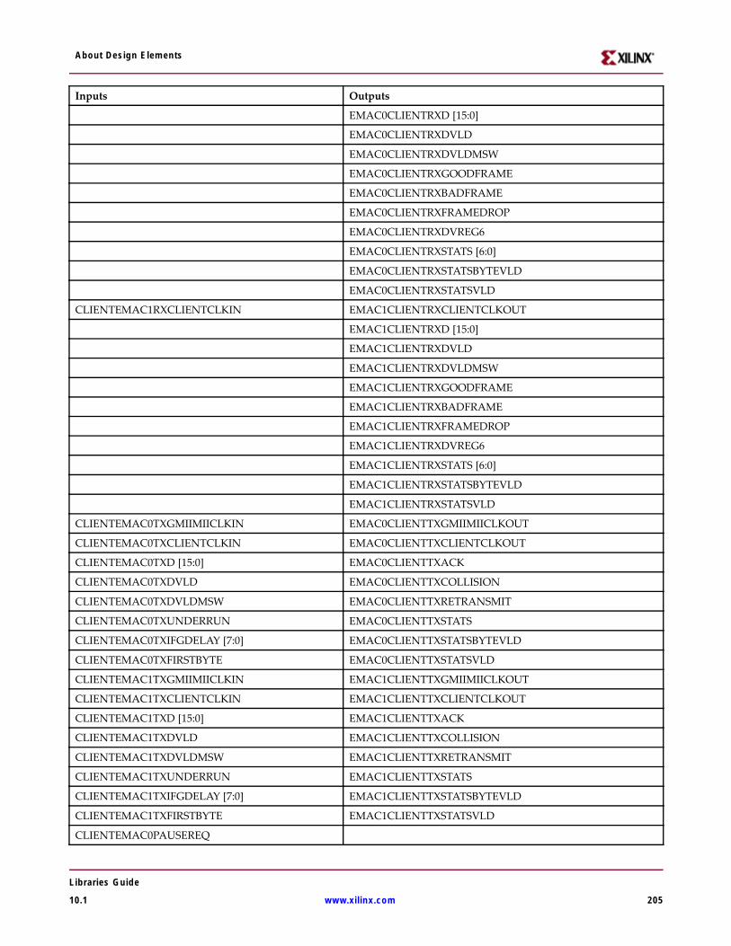
About Design Elements
Inputs Outputs
EMAC0CLIENTRXD [15:0]
EMAC0CLIENTRXDVLD
EMAC0CLIENTRXDVLDMSW
EMAC0CLIENTRXGOODFRAME
EMAC0CLIENTRXBADFRAME
EMAC0CLIENTRXFRAMEDROP
EMAC0CLIENTRXDVREG6
EMAC0CLIENTRXSTATS [6:0]
EMAC0CLIENTRXSTATSBYTEVLD
EMAC0CLIENTRXSTATSVLD
CLIENTEMAC1RXCLIENTCLKIN EMAC1CLIENTRXCLIENTCLKOUT
EMAC1CLIENTRXD [15:0]
EMAC1CLIENTRXDVLD
EMAC1CLIENTRXDVLDMSW
EMAC1CLIENTRXGOODFRAME
EMAC1CLIENTRXBADFRAME
EMAC1CLIENTRXFRAMEDROP
EMAC1CLIENTRXDVREG6
EMAC1CLIENTRXSTATS [6:0]
EMAC1CLIENTRXSTATSBYTEVLD
EMAC1CLIENTRXSTATSVLD
CLIENTEMAC0TXGMIIMIICLKIN EMAC0CLIENTTXGMIIMIICLKOUT
CLIENTEMAC0TXCLIENTCLKIN EMAC0CLIENTTXCLIENTCLKOUT
CLIENTEMAC0TXD [15:0] EMAC0CLIENTTXACK
CLIENTEMAC0TXDVLD EMAC0CLIENTTXCOLLISION
CLIENTEMAC0TXDVLDMSW EMAC0CLIENTTXRETRANSMIT
CLIENTEMAC0TXUNDERRUN EMAC0CLIENTTXSTATS
CLIENTEMAC0TXIFGDELAY [7:0] EMAC0CLIENTTXSTATSBYTEVLD
CLIENTEMAC0TXFIRSTBYTE EMAC0CLIENTTXSTATSVLD
CLIENTEMAC1TXGMIIMIICLKIN EMAC1CLIENTTXGMIIMIICLKOUT
CLIENTEMAC1TXCLIENTCLKIN EMAC1CLIENTTXCLIENTCLKOUT
CLIENTEMAC1TXD [15:0] EMAC1CLIENTTXACK
CLIENTEMAC1TXDVLD EMAC1CLIENTTXCOLLISION
CLIENTEMAC1TXDVLDMSW EMAC1CLIENTTXRETRANSMIT
CLIENTEMAC1TXUNDERRUN EMAC1CLIENTTXSTATS
CLIENTEMAC1TXIFGDELAY [7:0] EMAC1CLIENTTXSTATSBYTEVLD
CLIENTEMAC1TXFIRSTBYTE EMAC1CLIENTTXSTATSVLD
CLIENTEMAC0PAUSEREQ
Libraries Guide
10.1 www.xilinx.com 205

About Design Elements
Inputs Outputs
CLIENTEMAC0PAUSEVAL [15:0]
CLIENTEMAC1PAUSEREQ
CLIENTEMAC1PAUSEVAL [15:0]
HOSTADDR [9:0] HOSTMIIMRDY
HOSTCLK HOSTRDDATA [31:0]
HOSTMIIMSEL
HOSTOPCODE [1:0]
HOSTREQ
HOSTWRDATA [31:0]
HOSTEMAC1SEL
DCREMACCLK DCRHOSTDONEIR
DCREMACENABLE EMACDCRACK
DCREMACDBUS [0:31] EMACDCRDBUS [0:31]
DCREMACABUS [8:9]
DCREMACREAD
DCREMACWRITE
PHYEMAC0RXCLK EMAC0PHYTXCLK
PHYEMAC0RXD [7:0] EMAC0PHYTXD [7:0]
PHYEMAC0RXDV EMAC0PHYTXEN
PHYEMAC0RXER EMAC0PHYTXER
PHYEMAC0MIITXCLK
PHYEMAC0COL
PHYEMAC0CRS
PHYEMAC1RXCLK EMAC1PHYTXCLK
PHYEMAC1RXD [7:0] EMAC1PHYTXD [7:0]
PHYEMAC1RXDV EMAC1PHYTXEN
PHYEMAC1RXER EMAC1PHYTXER
PHYEMAC1MIITXCLK
PHYEMAC1COL
PHYEMAC1CRS
PHYEMAC0SIGNALDET EMAC0PHYENCOMMAALIGN
PHYEMAC0PHYAD [4:0] EMAC0PHYLOOPBACKMSB
PHYEMAC0RXCLKCORCNT [2:0] EMAC0PHYMGTRXRESET
PHYEMAC0RXBUFSTATUS [1:0] EMAC0PHYMGTTXRESET
PHYEMAC0RXCHARISCOMMA EMAC0PHYPOWERDOWN
PHYEMAC0RXCHARISK EMAC0PHYSYNCACQSTATUS
PHYEMAC0RXCHECKINGCRC EMAC0PHYTXCHARDISPMODE
PHYEMAC0RXCOMMADET EMAC0PHYTXCHARDISPVAL
Libraries Guide
206 www.xilinx.com 10.1
About Design Elements
Inputs Outputs
PHYEMAC0RXDISPERR EMAC0PHYTXCHARISK
PHYEMAC0RXLOSSOFSYNC [1:0]
PHYEMAC0RXNOTINTABLE
PHYEMAC0RXRUNDISP
PHYEMAC0RXBUFERR
PHYEMAC0TXBUFERR
PHYEMAC1SIGNALDET EMAC1PHYENCOMMAALIGN
PHYEMAC1PHYAD [4:0] EMAC1PHYLOOPBACKMSB
PHYEMAC1RXCLKCORCNT [2:0] EMAC1PHYMGTRXRESET
PHYEMAC1RXBUFSTATUS [1:0] EMAC1PHYMGTTXRESET
PHYEMAC1RXCHARISCOMMA EMAC1PHYPOWERDOWN
PHYEMAC1RXCHARISK EMAC1PHYSYNCACQSTATUS
PHYEMAC1RXCHECKINGCRC EMAC1PHYTXCHARDISPMODE
PHYEMAC1RXCOMMADET EMAC1PHYTXCHARDISPVAL
PHYEMAC1RXDISPERR EMAC1PHYTXCHARISK
PHYEMAC1RXLOSSOFSYNC [1:0]
PHYEMAC1RXNOTINTABLE
PHYEMAC1RXRUNDISP
PHYEMAC1RXBUFERR
PHYEMAC1TXBUFERR
PHYEMAC0MCLKIN EMAC0PHYMCLKOUT
PHYEMAC0MDIN EMAC0PHYMDOUT
EMAC0PHYMDTRI
PHYEMAC1MCLKIN EMAC1PHYMCLKOUT
PHYEMAC1MDIN EMAC1PHYMDOUT
EMAC1PHYMDTRI
Design Entry MethodThis design element can be used in schematics.
For More Information• See the Virtex-4 User Guide.
• See the Virtex-4 Data Sheets.
Libraries Guide
10.1 www.xilinx.com 207
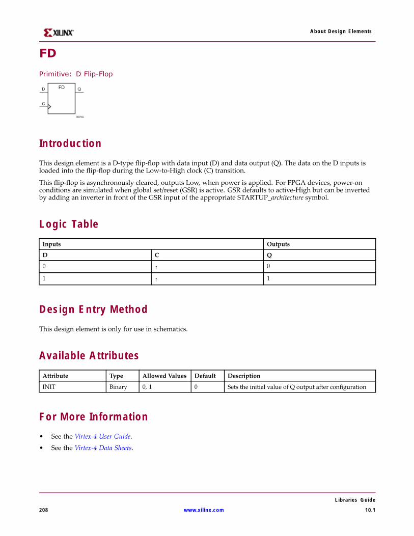
About Design Elements
FD
Primitive: D Flip-Flop
IntroductionThis design element is a D-type flip-flop with data input (D) and data output (Q). The data on the D inputs isloaded into the flip-flop during the Low-to-High clock (C) transition.
This flip-flop is asynchronously cleared, outputs Low, when power is applied. For FPGA devices, power-onconditions are simulated when global set/reset (GSR) is active. GSR defaults to active-High but can be invertedby adding an inverter in front of the GSR input of the appropriate STARTUP_architecture symbol.
Logic TableInputs Outputs
D C Q
0 ↑ 0
1 ↑ 1
Design Entry MethodThis design element is only for use in schematics.
Available AttributesAttribute Type Allowed Values Default Description
INIT Binary 0, 1 0 Sets the initial value of Q output after configuration
For More Information• See the Virtex-4 User Guide.
• See the Virtex-4 Data Sheets.
Libraries Guide
208 www.xilinx.com 10.1
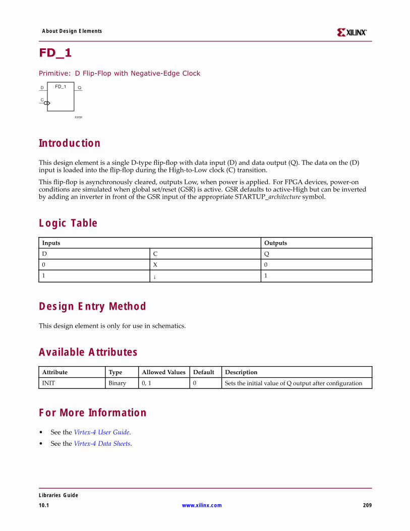
About Design Elements
FD_1
Primitive: D Flip-Flop with Negative-Edge Clock
IntroductionThis design element is a single D-type flip-flop with data input (D) and data output (Q). The data on the (D)input is loaded into the flip-flop during the High-to-Low clock (C) transition.
This flip-flop is asynchronously cleared, outputs Low, when power is applied. For FPGA devices, power-onconditions are simulated when global set/reset (GSR) is active. GSR defaults to active-High but can be invertedby adding an inverter in front of the GSR input of the appropriate STARTUP_architecture symbol.
Logic TableInputs Outputs
D C Q
0 X 0
1 ↓ 1
Design Entry MethodThis design element is only for use in schematics.
Available AttributesAttribute Type Allowed Values Default Description
INIT Binary 0, 1 0 Sets the initial value of Q output after configuration
For More Information• See the Virtex-4 User Guide.
• See the Virtex-4 Data Sheets.
Libraries Guide
10.1 www.xilinx.com 209
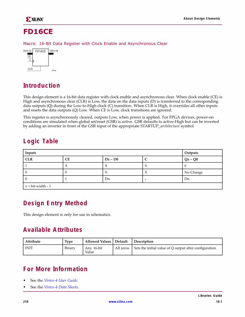
About Design Elements
FD16CE
Macro: 16-Bit Data Register with Clock Enable and Asynchronous Clear
IntroductionThis design element is a 16-bit data register with clock enable and asynchronous clear. When clock enable (CE) isHigh and asynchronous clear (CLR) is Low, the data on the data inputs (D) is transferred to the correspondingdata outputs (Q) during the Low-to-High clock (C) transition. When CLR is High, it overrides all other inputsand resets the data outputs (Q) Low. When CE is Low, clock transitions are ignored.
This register is asynchronously cleared, outputs Low, when power is applied. For FPGA devices, power-onconditions are simulated when global set/reset (GSR) is active. GSR defaults to active-High but can be invertedby adding an inverter in front of the GSR input of the appropriate STARTUP_architecture symbol.
Logic TableInputs Outputs
CLR CE Dz – D0 C Qz – Q0
1 X X X 0
0 0 X X No Change
0 1 Dn ↑ Dn
z = bit-width - 1
Design Entry MethodThis design element is only for use in schematics.
Available AttributesAttribute Type Allowed Values Default Description
INIT Binary Any 16-bitValue
All zeros Sets the initial value of Q output after configuration
For More Information• See the Virtex-4 User Guide.• See the Virtex-4 Data Sheets.
Libraries Guide
210 www.xilinx.com 10.1
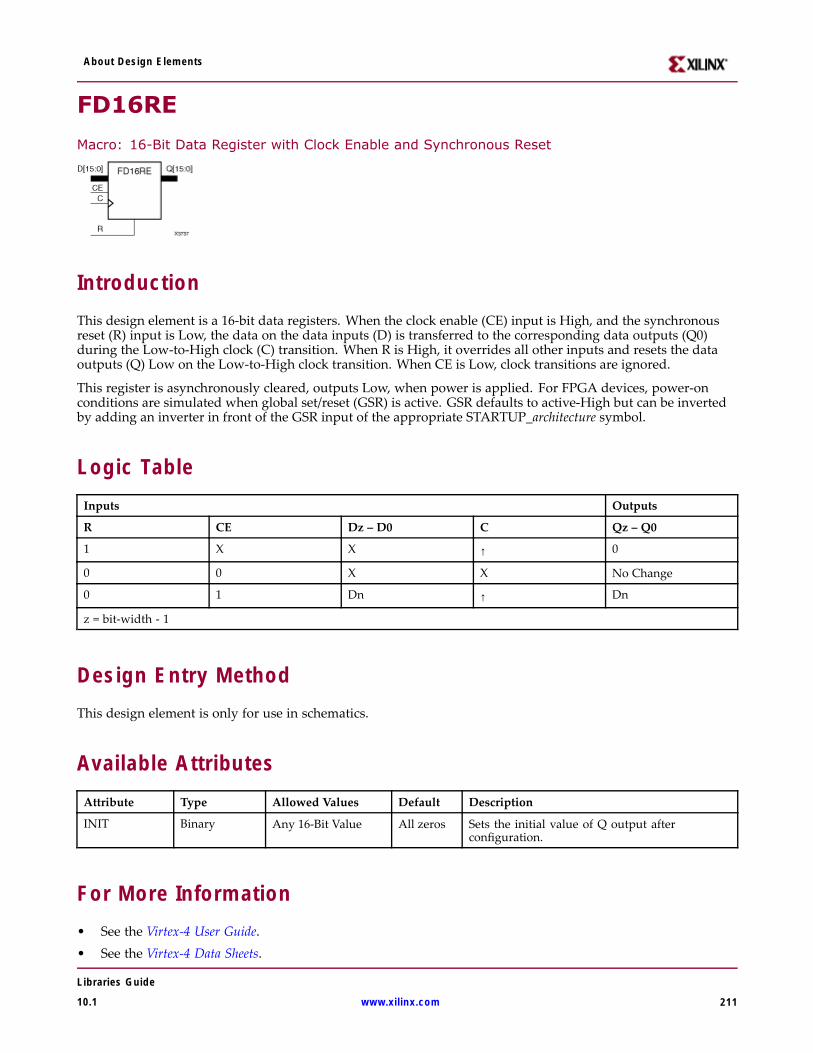
About Design Elements
FD16RE
Macro: 16-Bit Data Register with Clock Enable and Synchronous Reset
IntroductionThis design element is a 16-bit data registers. When the clock enable (CE) input is High, and the synchronousreset (R) input is Low, the data on the data inputs (D) is transferred to the corresponding data outputs (Q0)during the Low-to-High clock (C) transition. When R is High, it overrides all other inputs and resets the dataoutputs (Q) Low on the Low-to-High clock transition. When CE is Low, clock transitions are ignored.
This register is asynchronously cleared, outputs Low, when power is applied. For FPGA devices, power-onconditions are simulated when global set/reset (GSR) is active. GSR defaults to active-High but can be invertedby adding an inverter in front of the GSR input of the appropriate STARTUP_architecture symbol.
Logic TableInputs Outputs
R CE Dz – D0 C Qz – Q0
1 X X ↑ 0
0 0 X X No Change
0 1 Dn ↑ Dn
z = bit-width - 1
Design Entry MethodThis design element is only for use in schematics.
Available AttributesAttribute Type Allowed Values Default Description
INIT Binary Any 16-Bit Value All zeros Sets the initial value of Q output afterconfiguration.
For More Information• See the Virtex-4 User Guide.• See the Virtex-4 Data Sheets.
Libraries Guide
10.1 www.xilinx.com 211
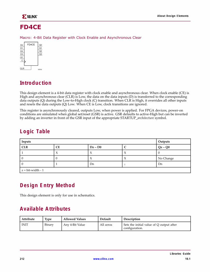
About Design Elements
FD4CE
Macro: 4-Bit Data Register with Clock Enable and Asynchronous Clear
IntroductionThis design element is a 4-bit data register with clock enable and asynchronous clear. When clock enable (CE) isHigh and asynchronous clear (CLR) is Low, the data on the data inputs (D) is transferred to the correspondingdata outputs (Q) during the Low-to-High clock (C) transition. When CLR is High, it overrides all other inputsand resets the data outputs (Q) Low. When CE is Low, clock transitions are ignored.
This register is asynchronously cleared, outputs Low, when power is applied. For FPGA devices, power-onconditions are simulated when global set/reset (GSR) is active. GSR defaults to active-High but can be invertedby adding an inverter in front of the GSR input of the appropriate STARTUP_architecture symbol.
Logic TableInputs Outputs
CLR CE Dz – D0 C Qz – Q0
1 X X X 0
0 0 X X No Change
0 1 Dn ↑ Dn
z = bit-width - 1
Design Entry MethodThis design element is only for use in schematics.
Available AttributesAttribute Type Allowed Values Default Description
INIT Binary Any 4-Bit Value All zeros Sets the initial value of Q output afterconfiguration.
Libraries Guide
212 www.xilinx.com 10.1

About Design Elements
For More Information• See the Virtex-4 User Guide.
• See the Virtex-4 Data Sheets.
Libraries Guide
10.1 www.xilinx.com 213
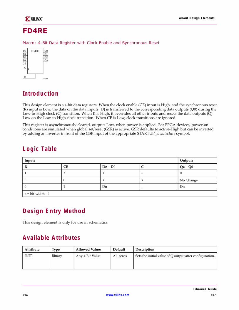
About Design Elements
FD4RE
Macro: 4-Bit Data Register with Clock Enable and Synchronous Reset
IntroductionThis design element is a 4-bit data registers. When the clock enable (CE) input is High, and the synchronous reset(R) input is Low, the data on the data inputs (D) is transferred to the corresponding data outputs (Q0) during theLow-to-High clock (C) transition. When R is High, it overrides all other inputs and resets the data outputs (Q)Low on the Low-to-High clock transition. When CE is Low, clock transitions are ignored.
This register is asynchronously cleared, outputs Low, when power is applied. For FPGA devices, power-onconditions are simulated when global set/reset (GSR) is active. GSR defaults to active-High but can be invertedby adding an inverter in front of the GSR input of the appropriate STARTUP_architecture symbol.
Logic TableInputs Outputs
R CE Dz – D0 C Qz – Q0
1 X X ↑ 0
0 0 X X No Change
0 1 Dn ↑ Dn
z = bit-width - 1
Design Entry MethodThis design element is only for use in schematics.
Available AttributesAttribute Type Allowed Values Default Description
INIT Binary Any 4-Bit Value All zeros Sets the initial value of Q output after configuration.
Libraries Guide
214 www.xilinx.com 10.1

About Design Elements
For More Information• See the Virtex-4 User Guide.
• See the Virtex-4 Data Sheets.
Libraries Guide
10.1 www.xilinx.com 215
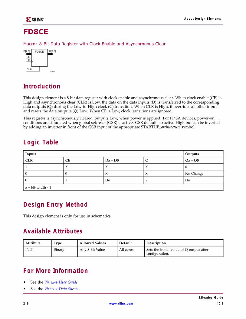
About Design Elements
FD8CE
Macro: 8-Bit Data Register with Clock Enable and Asynchronous Clear
IntroductionThis design element is a 8-bit data register with clock enable and asynchronous clear. When clock enable (CE) isHigh and asynchronous clear (CLR) is Low, the data on the data inputs (D) is transferred to the correspondingdata outputs (Q) during the Low-to-High clock (C) transition. When CLR is High, it overrides all other inputsand resets the data outputs (Q) Low. When CE is Low, clock transitions are ignored.
This register is asynchronously cleared, outputs Low, when power is applied. For FPGA devices, power-onconditions are simulated when global set/reset (GSR) is active. GSR defaults to active-High but can be invertedby adding an inverter in front of the GSR input of the appropriate STARTUP_architecture symbol.
Logic TableInputs Outputs
CLR CE Dz – D0 C Qz – Q0
1 X X X 0
0 0 X X No Change
0 1 Dn ↑ Dn
z = bit-width - 1
Design Entry MethodThis design element is only for use in schematics.
Available AttributesAttribute Type Allowed Values Default Description
INIT Binary Any 8-Bit Value All zeros Sets the initial value of Q output afterconfiguration.
For More Information• See the Virtex-4 User Guide.• See the Virtex-4 Data Sheets.
Libraries Guide
216 www.xilinx.com 10.1
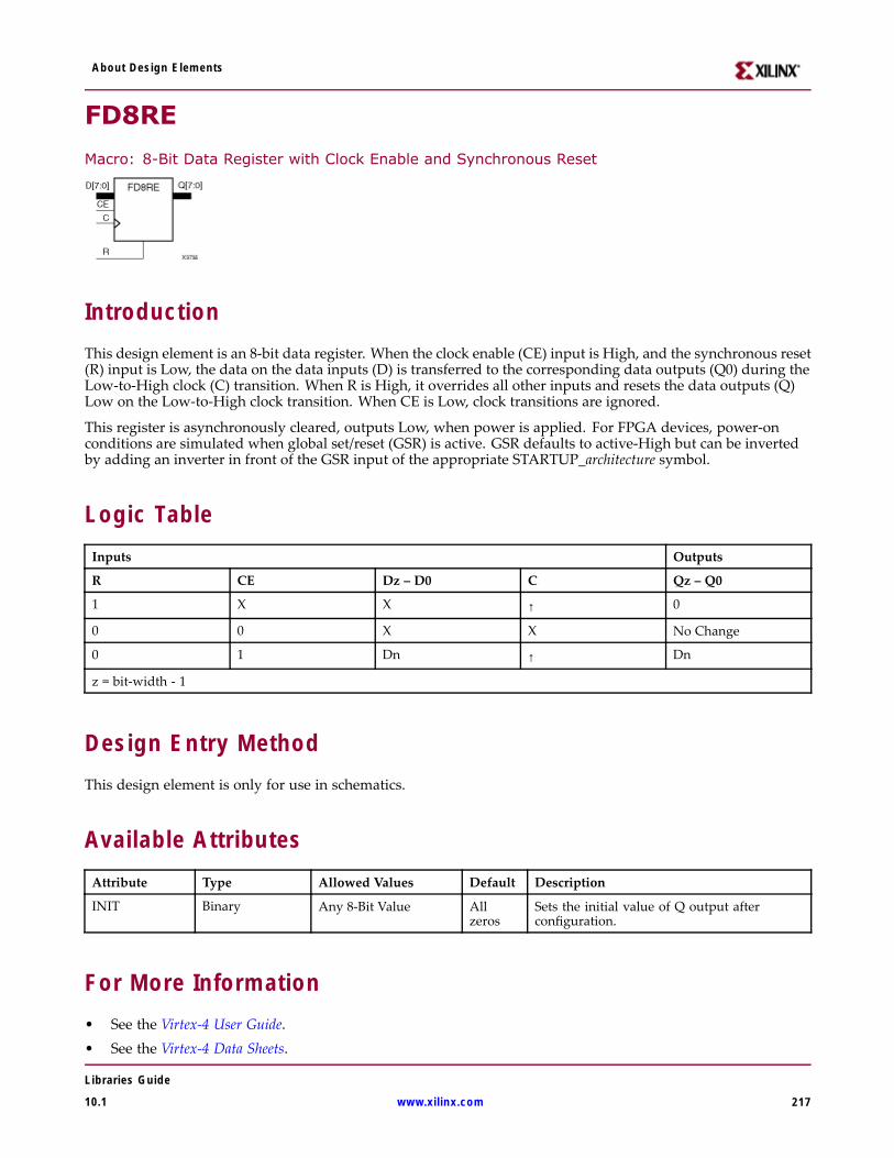
About Design Elements
FD8RE
Macro: 8-Bit Data Register with Clock Enable and Synchronous Reset
IntroductionThis design element is an 8-bit data register. When the clock enable (CE) input is High, and the synchronous reset(R) input is Low, the data on the data inputs (D) is transferred to the corresponding data outputs (Q0) during theLow-to-High clock (C) transition. When R is High, it overrides all other inputs and resets the data outputs (Q)Low on the Low-to-High clock transition. When CE is Low, clock transitions are ignored.
This register is asynchronously cleared, outputs Low, when power is applied. For FPGA devices, power-onconditions are simulated when global set/reset (GSR) is active. GSR defaults to active-High but can be invertedby adding an inverter in front of the GSR input of the appropriate STARTUP_architecture symbol.
Logic TableInputs Outputs
R CE Dz – D0 C Qz – Q0
1 X X ↑ 0
0 0 X X No Change
0 1 Dn ↑ Dn
z = bit-width - 1
Design Entry MethodThis design element is only for use in schematics.
Available AttributesAttribute Type Allowed Values Default Description
INIT Binary Any 8-Bit Value Allzeros
Sets the initial value of Q output afterconfiguration.
For More Information• See the Virtex-4 User Guide.• See the Virtex-4 Data Sheets.
Libraries Guide
10.1 www.xilinx.com 217
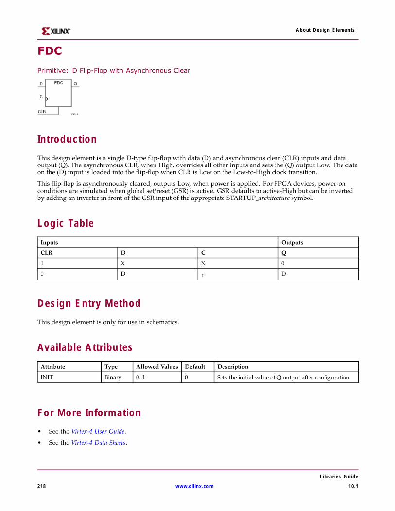
About Design Elements
FDC
Primitive: D Flip-Flop with Asynchronous Clear
IntroductionThis design element is a single D-type flip-flop with data (D) and asynchronous clear (CLR) inputs and dataoutput (Q). The asynchronous CLR, when High, overrides all other inputs and sets the (Q) output Low. The dataon the (D) input is loaded into the flip-flop when CLR is Low on the Low-to-High clock transition.
This flip-flop is asynchronously cleared, outputs Low, when power is applied. For FPGA devices, power-onconditions are simulated when global set/reset (GSR) is active. GSR defaults to active-High but can be invertedby adding an inverter in front of the GSR input of the appropriate STARTUP_architecture symbol.
Logic TableInputs Outputs
CLR D C Q
1 X X 0
0 D ↑ D
Design Entry MethodThis design element is only for use in schematics.
Available AttributesAttribute Type Allowed Values Default Description
INIT Binary 0, 1 0 Sets the initial value of Q output after configuration
For More Information• See the Virtex-4 User Guide.
• See the Virtex-4 Data Sheets.
Libraries Guide
218 www.xilinx.com 10.1
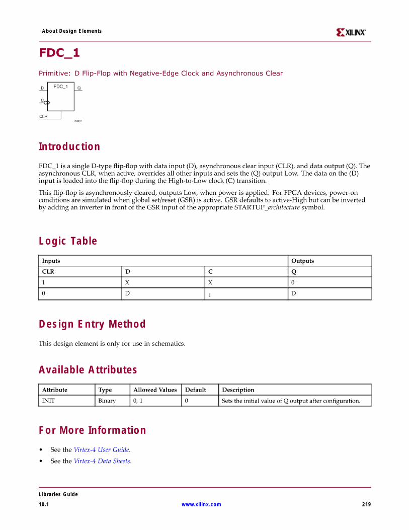
About Design Elements
FDC_1
Primitive: D Flip-Flop with Negative-Edge Clock and Asynchronous Clear
IntroductionFDC_1 is a single D-type flip-flop with data input (D), asynchronous clear input (CLR), and data output (Q). Theasynchronous CLR, when active, overrides all other inputs and sets the (Q) output Low. The data on the (D)input is loaded into the flip-flop during the High-to-Low clock (C) transition.
This flip-flop is asynchronously cleared, outputs Low, when power is applied. For FPGA devices, power-onconditions are simulated when global set/reset (GSR) is active. GSR defaults to active-High but can be invertedby adding an inverter in front of the GSR input of the appropriate STARTUP_architecture symbol.
Logic TableInputs Outputs
CLR D C Q
1 X X 0
0 D ↓ D
Design Entry MethodThis design element is only for use in schematics.
Available AttributesAttribute Type Allowed Values Default Description
INIT Binary 0, 1 0 Sets the initial value of Q output after configuration.
For More Information• See the Virtex-4 User Guide.
• See the Virtex-4 Data Sheets.
Libraries Guide
10.1 www.xilinx.com 219
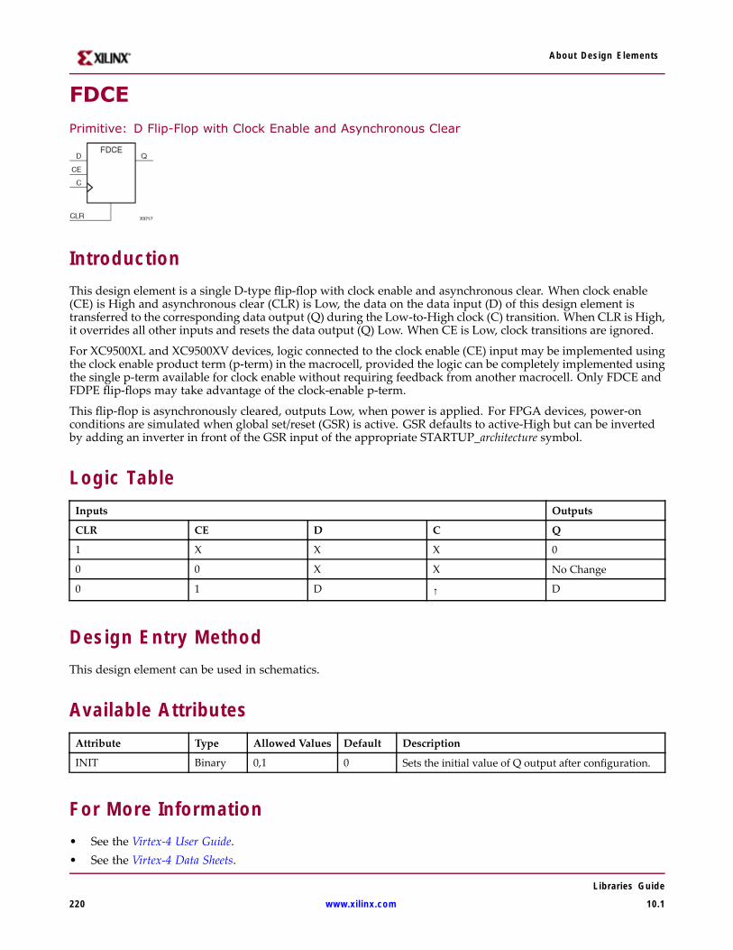
About Design Elements
FDCEPrimitive: D Flip-Flop with Clock Enable and Asynchronous Clear
IntroductionThis design element is a single D-type flip-flop with clock enable and asynchronous clear. When clock enable(CE) is High and asynchronous clear (CLR) is Low, the data on the data input (D) of this design element istransferred to the corresponding data output (Q) during the Low-to-High clock (C) transition. When CLR is High,it overrides all other inputs and resets the data output (Q) Low. When CE is Low, clock transitions are ignored.
For XC9500XL and XC9500XV devices, logic connected to the clock enable (CE) input may be implemented usingthe clock enable product term (p-term) in the macrocell, provided the logic can be completely implemented usingthe single p-term available for clock enable without requiring feedback from another macrocell. Only FDCE andFDPE flip-flops may take advantage of the clock-enable p-term.
This flip-flop is asynchronously cleared, outputs Low, when power is applied. For FPGA devices, power-onconditions are simulated when global set/reset (GSR) is active. GSR defaults to active-High but can be invertedby adding an inverter in front of the GSR input of the appropriate STARTUP_architecture symbol.
Logic TableInputs Outputs
CLR CE D C Q
1 X X X 0
0 0 X X No Change
0 1 D ↑ D
Design Entry MethodThis design element can be used in schematics.
Available AttributesAttribute Type Allowed Values Default Description
INIT Binary 0,1 0 Sets the initial value of Q output after configuration.
For More Information• See the Virtex-4 User Guide.• See the Virtex-4 Data Sheets.
Libraries Guide
220 www.xilinx.com 10.1
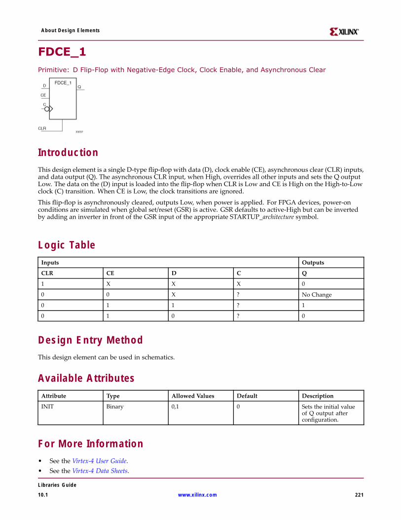
About Design Elements
FDCE_1Primitive: D Flip-Flop with Negative-Edge Clock, Clock Enable, and Asynchronous Clear
IntroductionThis design element is a single D-type flip-flop with data (D), clock enable (CE), asynchronous clear (CLR) inputs,and data output (Q). The asynchronous CLR input, when High, overrides all other inputs and sets the Q outputLow. The data on the (D) input is loaded into the flip-flop when CLR is Low and CE is High on the High-to-Lowclock (C) transition. When CE is Low, the clock transitions are ignored.
This flip-flop is asynchronously cleared, outputs Low, when power is applied. For FPGA devices, power-onconditions are simulated when global set/reset (GSR) is active. GSR defaults to active-High but can be invertedby adding an inverter in front of the GSR input of the appropriate STARTUP_architecture symbol.
Logic TableInputs Outputs
CLR CE D C Q
1 X X X 0
0 0 X ? No Change
0 1 1 ? 1
0 1 0 ? 0
Design Entry MethodThis design element can be used in schematics.
Available AttributesAttribute Type Allowed Values Default Description
INIT Binary 0,1 0 Sets the initial valueof Q output afterconfiguration.
For More Information• See the Virtex-4 User Guide.• See the Virtex-4 Data Sheets.
Libraries Guide
10.1 www.xilinx.com 221
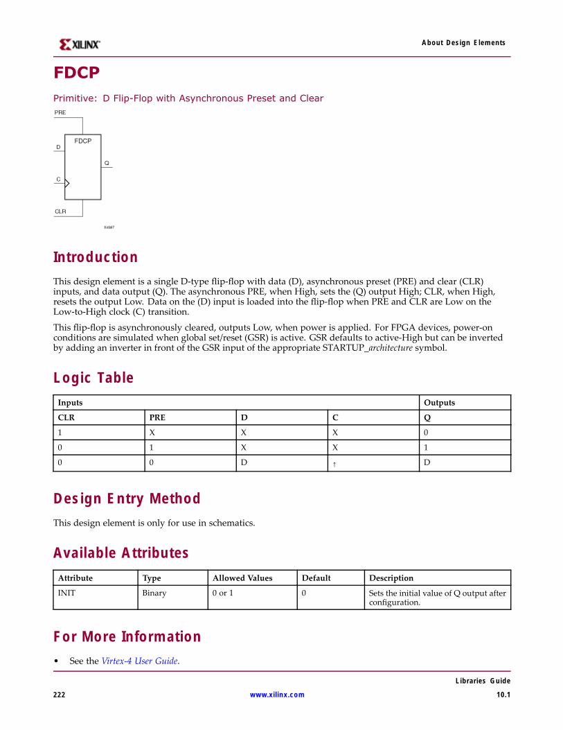
About Design Elements
FDCPPrimitive: D Flip-Flop with Asynchronous Preset and Clear
IntroductionThis design element is a single D-type flip-flop with data (D), asynchronous preset (PRE) and clear (CLR)inputs, and data output (Q). The asynchronous PRE, when High, sets the (Q) output High; CLR, when High,resets the output Low. Data on the (D) input is loaded into the flip-flop when PRE and CLR are Low on theLow-to-High clock (C) transition.
This flip-flop is asynchronously cleared, outputs Low, when power is applied. For FPGA devices, power-onconditions are simulated when global set/reset (GSR) is active. GSR defaults to active-High but can be invertedby adding an inverter in front of the GSR input of the appropriate STARTUP_architecture symbol.
Logic TableInputs Outputs
CLR PRE D C Q
1 X X X 0
0 1 X X 1
0 0 D ↑ D
Design Entry MethodThis design element is only for use in schematics.
Available AttributesAttribute Type Allowed Values Default Description
INIT Binary 0 or 1 0 Sets the initial value of Q output afterconfiguration.
For More Information• See the Virtex-4 User Guide.
Libraries Guide
222 www.xilinx.com 10.1

About Design Elements
• See the Virtex-4 Data Sheets.
Libraries Guide
10.1 www.xilinx.com 223
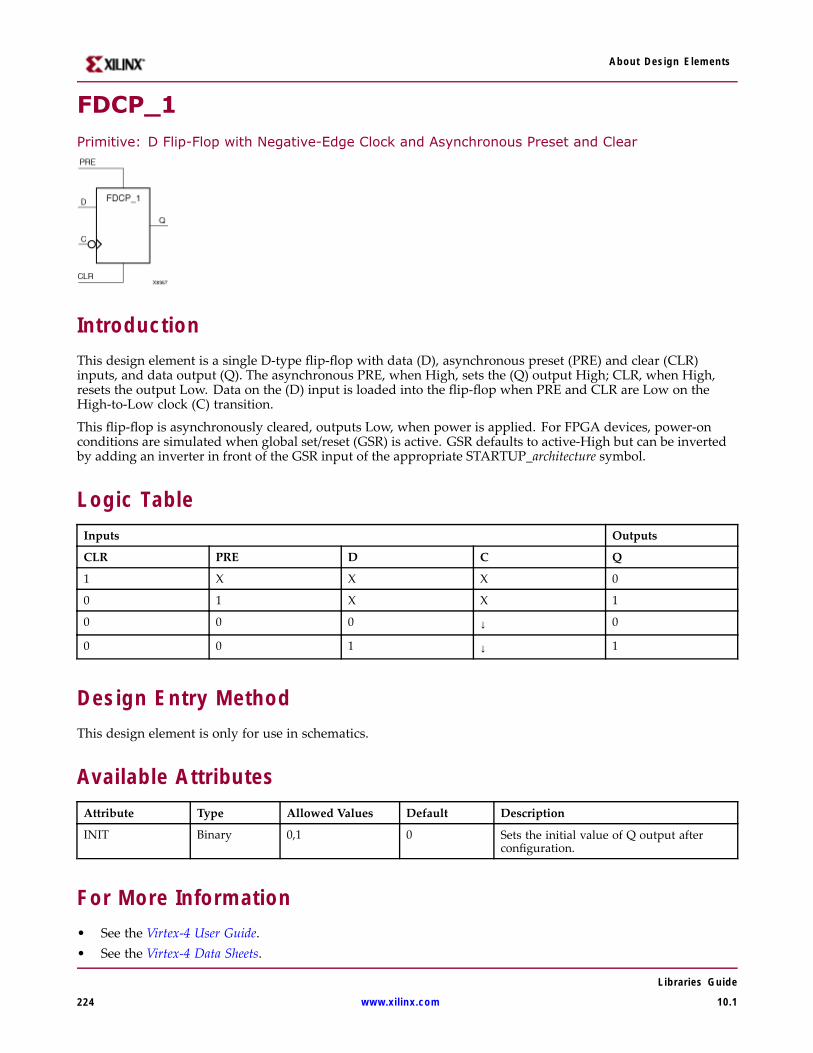
About Design Elements
FDCP_1Primitive: D Flip-Flop with Negative-Edge Clock and Asynchronous Preset and Clear
IntroductionThis design element is a single D-type flip-flop with data (D), asynchronous preset (PRE) and clear (CLR)inputs, and data output (Q). The asynchronous PRE, when High, sets the (Q) output High; CLR, when High,resets the output Low. Data on the (D) input is loaded into the flip-flop when PRE and CLR are Low on theHigh-to-Low clock (C) transition.
This flip-flop is asynchronously cleared, outputs Low, when power is applied. For FPGA devices, power-onconditions are simulated when global set/reset (GSR) is active. GSR defaults to active-High but can be invertedby adding an inverter in front of the GSR input of the appropriate STARTUP_architecture symbol.
Logic TableInputs Outputs
CLR PRE D C Q
1 X X X 0
0 1 X X 1
0 0 0 ↓ 0
0 0 1 ↓ 1
Design Entry MethodThis design element is only for use in schematics.
Available AttributesAttribute Type Allowed Values Default Description
INIT Binary 0,1 0 Sets the initial value of Q output afterconfiguration.
For More Information• See the Virtex-4 User Guide.• See the Virtex-4 Data Sheets.
Libraries Guide
224 www.xilinx.com 10.1
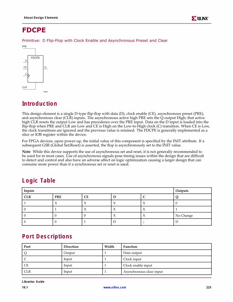
About Design Elements
FDCPEPrimitive: D Flip-Flop with Clock Enable and Asynchronous Preset and Clear
IntroductionThis design element is a single D-type flip-flop with data (D), clock enable (CE), asynchronous preset (PRE),and asynchronous clear (CLR) inputs. The asynchronous active high PRE sets the Q output High; that activehigh CLR resets the output Low and has precedence over the PRE input. Data on the D input is loaded into theflip-flop when PRE and CLR are Low and CE is High on the Low-to-High clock (C) transition. When CE is Low,the clock transitions are ignored and the previous value is retained. The FDCPE is generally implemented as aslice or IOB register within the device.
For FPGA devices, upon power-up, the initial value of this component is specified by the INIT attribute. If asubsequent GSR (Global Set/Reset) is asserted, the flop is asynchronously set to the INIT value.
Note While this device supports the use of asynchronous set and reset, it is not generally recommended tobe used for in most cases. Use of asynchronous signals pose timing issues within the design that are difficultto detect and control and also have an adverse affect on logic optimization causing a larger design that canconsume more power than if a synchronous set or reset is used.
Logic TableInputs Outputs
CLR PRE CE D C Q
1 X X X X 0
0 1 X X X 1
0 0 0 X X No Change
0 0 1 D ↑ D
Port DescriptionsPort Direction Width Function
Q Output 1 Data output
C Input 1 Clock input
CE Input 1 Clock enable input
CLR Input 1 Asynchronous clear input
Libraries Guide
10.1 www.xilinx.com 225
About Design Elements
Port Direction Width Function
D Input 1 Data input
PRE Input 1 Asynchronous set input
Design Entry MethodThis design element can be used in schematics.
Available AttributesAttribute Type Allowed Values Default Description
INIT Binary 0,1 0 Sets the initial value of Q output afterconfiguration and on GSR.
Libraries Guide
226 www.xilinx.com 10.1

About Design Elements
For More Information• See the Virtex-4 User Guide.
• See the Virtex-4 Data Sheets.
Libraries Guide
10.1 www.xilinx.com 227
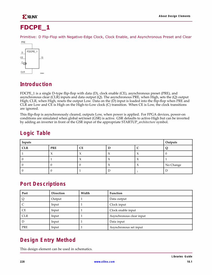
About Design Elements
FDCPE_1Primitive: D Flip-Flop with Negative-Edge Clock, Clock Enable, and Asynchronous Preset and Clear
IntroductionFDCPE_1 is a single D-type flip-flop with data (D), clock enable (CE), asynchronous preset (PRE), andasynchronous clear (CLR) inputs and data output (Q). The asynchronous PRE, when High, sets the (Q) outputHigh; CLR, when High, resets the output Low. Data on the (D) input is loaded into the flip-flop when PRE andCLR are Low and CE is High on the High-to-Low clock (C) transition. When CE is Low, the clock transitionsare ignored.
This flip-flop is asynchronously cleared, outputs Low, when power is applied. For FPGA devices, power-onconditions are simulated when global set/reset (GSR) is active. GSR defaults to active-High but can be invertedby adding an inverter in front of the GSR input of the appropriate STARTUP_architecture symbol.
Logic TableInputs Outputs
CLR PRE CE D C Q
1 X X X X 0
0 1 X X X 1
0 0 0 X X No Change
0 0 1 D ↓ D
Port DescriptionsPort Direction Width Function
Q Output 1 Data output
C Input 1 Clock input
CE Input 1 Clock enable input
CLR Input 1 Asynchronous clear input
D Input 1 Data input
PRE Input 1 Asynchronous set input
Design Entry MethodThis design element can be used in schematics.
Libraries Guide
228 www.xilinx.com 10.1
About Design Elements
Available AttributesAttribute Type Allowed Values Default Description
INIT Binary 0,1 0 Sets the initial value of Q output afterconfiguration.
For More Information• See the Virtex-4 User Guide.
• See the Virtex-4 Data Sheets.
Libraries Guide
10.1 www.xilinx.com 229

About Design Elements
FDE
Primitive: D Flip-Flop with Clock Enable
IntroductionThis design element is a single D-type flip-flop with data input (D), clock enable (CE), and data output (Q).When clock enable is High, the data on the (D) input is loaded into the flip-flop during the Low-to-High clock(C) transition.
This flip-flop is asynchronously cleared, outputs Low, when power is applied. For FPGA devices, power-onconditions are simulated when global set/reset (GSR) is active. GSR defaults to active-High but can be invertedby adding an inverter in front of the GSR input of the appropriate STARTUP_architecture symbol.
Logic TableInputs Outputs
CE D C Q
0 X X No Change
1 0 ↑ 0
1 1 ↑ 1
Design Entry MethodThis design element is only for use in schematics.
Available Attributes
Attribute TypeAllowedValues Default Description
INIT Binary 0 or 1 0 Sets the initial value of Q output after configuration
For More Information• See the Virtex-4 User Guide.
• See the Virtex-4 Data Sheets.
Libraries Guide
230 www.xilinx.com 10.1
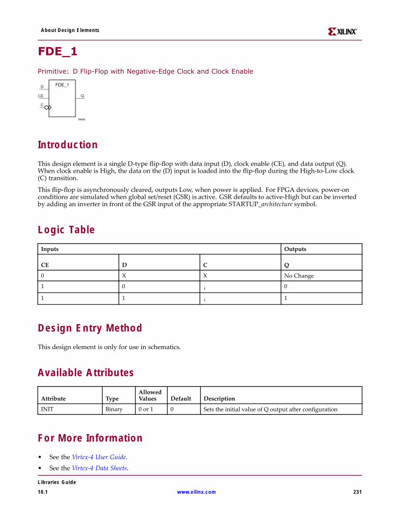
About Design Elements
FDE_1
Primitive: D Flip-Flop with Negative-Edge Clock and Clock Enable
IntroductionThis design element is a single D-type flip-flop with data input (D), clock enable (CE), and data output (Q).When clock enable is High, the data on the (D) input is loaded into the flip-flop during the High-to-Low clock(C) transition.
This flip-flop is asynchronously cleared, outputs Low, when power is applied. For FPGA devices, power-onconditions are simulated when global set/reset (GSR) is active. GSR defaults to active-High but can be invertedby adding an inverter in front of the GSR input of the appropriate STARTUP_architecture symbol.
Logic TableInputs Outputs
CE D C Q
0 X X No Change
1 0 ↓ 0
1 1 ↓ 1
Design Entry MethodThis design element is only for use in schematics.
Available Attributes
Attribute TypeAllowedValues Default Description
INIT Binary 0 or 1 0 Sets the initial value of Q output after configuration
For More Information• See the Virtex-4 User Guide.
• See the Virtex-4 Data Sheets.
Libraries Guide
10.1 www.xilinx.com 231
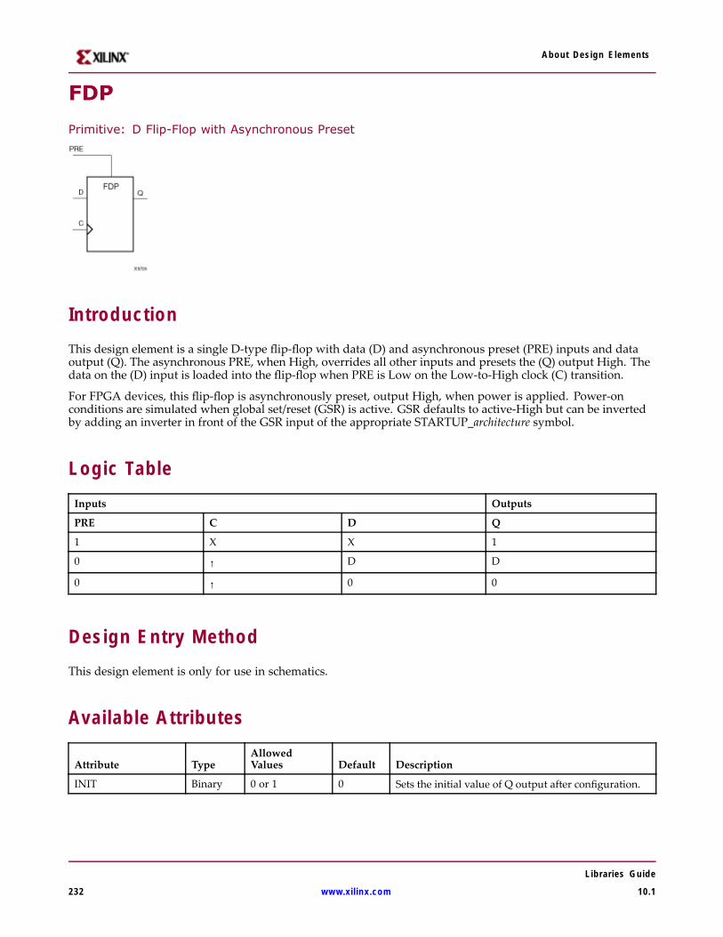
About Design Elements
FDP
Primitive: D Flip-Flop with Asynchronous Preset
IntroductionThis design element is a single D-type flip-flop with data (D) and asynchronous preset (PRE) inputs and dataoutput (Q). The asynchronous PRE, when High, overrides all other inputs and presets the (Q) output High. Thedata on the (D) input is loaded into the flip-flop when PRE is Low on the Low-to-High clock (C) transition.
For FPGA devices, this flip-flop is asynchronously preset, output High, when power is applied. Power-onconditions are simulated when global set/reset (GSR) is active. GSR defaults to active-High but can be invertedby adding an inverter in front of the GSR input of the appropriate STARTUP_architecture symbol.
Logic TableInputs Outputs
PRE C D Q
1 X X 1
0 ↑ D D
0 ↑ 0 0
Design Entry MethodThis design element is only for use in schematics.
Available Attributes
Attribute TypeAllowedValues Default Description
INIT Binary 0 or 1 0 Sets the initial value of Q output after configuration.
Libraries Guide
232 www.xilinx.com 10.1

About Design Elements
For More Information• See the Virtex-4 User Guide.
• See the Virtex-4 Data Sheets.
Libraries Guide
10.1 www.xilinx.com 233
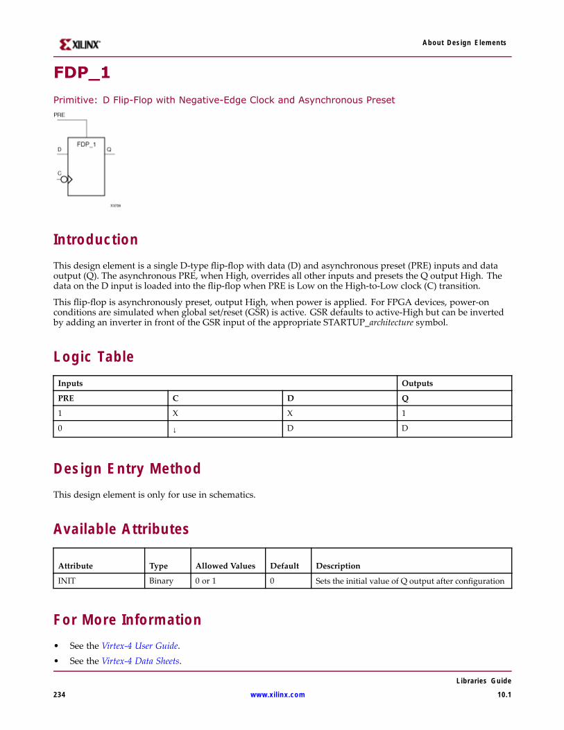
About Design Elements
FDP_1
Primitive: D Flip-Flop with Negative-Edge Clock and Asynchronous Preset
IntroductionThis design element is a single D-type flip-flop with data (D) and asynchronous preset (PRE) inputs and dataoutput (Q). The asynchronous PRE, when High, overrides all other inputs and presets the Q output High. Thedata on the D input is loaded into the flip-flop when PRE is Low on the High-to-Low clock (C) transition.
This flip-flop is asynchronously preset, output High, when power is applied. For FPGA devices, power-onconditions are simulated when global set/reset (GSR) is active. GSR defaults to active-High but can be invertedby adding an inverter in front of the GSR input of the appropriate STARTUP_architecture symbol.
Logic TableInputs Outputs
PRE C D Q
1 X X 1
0 ↓ D D
Design Entry MethodThis design element is only for use in schematics.
Available Attributes
Attribute Type Allowed Values Default Description
INIT Binary 0 or 1 0 Sets the initial value of Q output after configuration
For More Information• See the Virtex-4 User Guide.• See the Virtex-4 Data Sheets.
Libraries Guide
234 www.xilinx.com 10.1
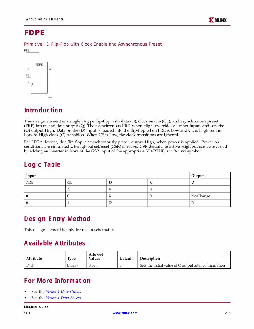
About Design Elements
FDPEPrimitive: D Flip-Flop with Clock Enable and Asynchronous Preset
IntroductionThis design element is a single D-type flip-flop with data (D), clock enable (CE), and asynchronous preset(PRE) inputs and data output (Q). The asynchronous PRE, when High, overrides all other inputs and sets the(Q) output High. Data on the (D) input is loaded into the flip-flop when PRE is Low and CE is High on theLow-to-High clock (C) transition. When CE is Low, the clock transitions are ignored.
For FPGA devices, this flip-flop is asynchronously preset, output High, when power is applied. Power-onconditions are simulated when global set/reset (GSR) is active. GSR defaults to active-High but can be invertedby adding an inverter in front of the GSR input of the appropriate STARTUP_architecture symbol.
Logic TableInputs Outputs
PRE CE D C Q
1 X X X 1
0 0 X X No Change
0 1 D ↑ D
Design Entry MethodThis design element is only for use in schematics.
Available Attributes
Attribute TypeAllowedValues Default Description
INIT Binary 0 or 1 0 Sets the initial value of Q output after configuration
For More Information• See the Virtex-4 User Guide.• See the Virtex-4 Data Sheets.
Libraries Guide
10.1 www.xilinx.com 235
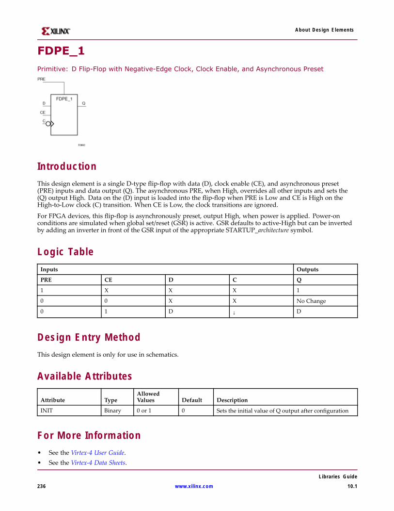
About Design Elements
FDPE_1Primitive: D Flip-Flop with Negative-Edge Clock, Clock Enable, and Asynchronous Preset
IntroductionThis design element is a single D-type flip-flop with data (D), clock enable (CE), and asynchronous preset(PRE) inputs and data output (Q). The asynchronous PRE, when High, overrides all other inputs and sets the(Q) output High. Data on the (D) input is loaded into the flip-flop when PRE is Low and CE is High on theHigh-to-Low clock (C) transition. When CE is Low, the clock transitions are ignored.
For FPGA devices, this flip-flop is asynchronously preset, output High, when power is applied. Power-onconditions are simulated when global set/reset (GSR) is active. GSR defaults to active-High but can be invertedby adding an inverter in front of the GSR input of the appropriate STARTUP_architecture symbol.
Logic TableInputs Outputs
PRE CE D C Q
1 X X X 1
0 0 X X No Change
0 1 D ↓ D
Design Entry MethodThis design element is only for use in schematics.
Available Attributes
Attribute TypeAllowedValues Default Description
INIT Binary 0 or 1 0 Sets the initial value of Q output after configuration
For More Information• See the Virtex-4 User Guide.• See the Virtex-4 Data Sheets.
Libraries Guide
236 www.xilinx.com 10.1
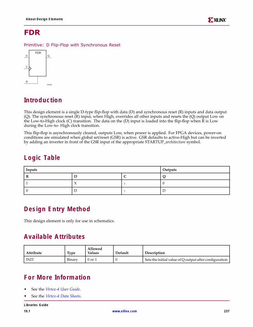
About Design Elements
FDR
Primitive: D Flip-Flop with Synchronous Reset
IntroductionThis design element is a single D-type flip-flop with data (D) and synchronous reset (R) inputs and data output(Q). The synchronous reset (R) input, when High, overrides all other inputs and resets the (Q) output Low onthe Low-to-High clock (C) transition. The data on the (D) input is loaded into the flip-flop when R is Lowduring the Low-to- High clock transition.
This flip-flop is asynchronously cleared, outputs Low, when power is applied. For FPGA devices, power-onconditions are simulated when global set/reset (GSR) is active. GSR defaults to active-High but can be invertedby adding an inverter in front of the GSR input of the appropriate STARTUP_architecture symbol.
Logic TableInputs Outputs
R D C Q
1 X ↑ 0
0 D ↑ D
Design Entry MethodThis design element is only for use in schematics.
Available Attributes
Attribute TypeAllowedValues Default Description
INIT Binary 0 or 1 0 Sets the initial value ofQ output after configuration
For More Information• See the Virtex-4 User Guide.• See the Virtex-4 Data Sheets.
Libraries Guide
10.1 www.xilinx.com 237
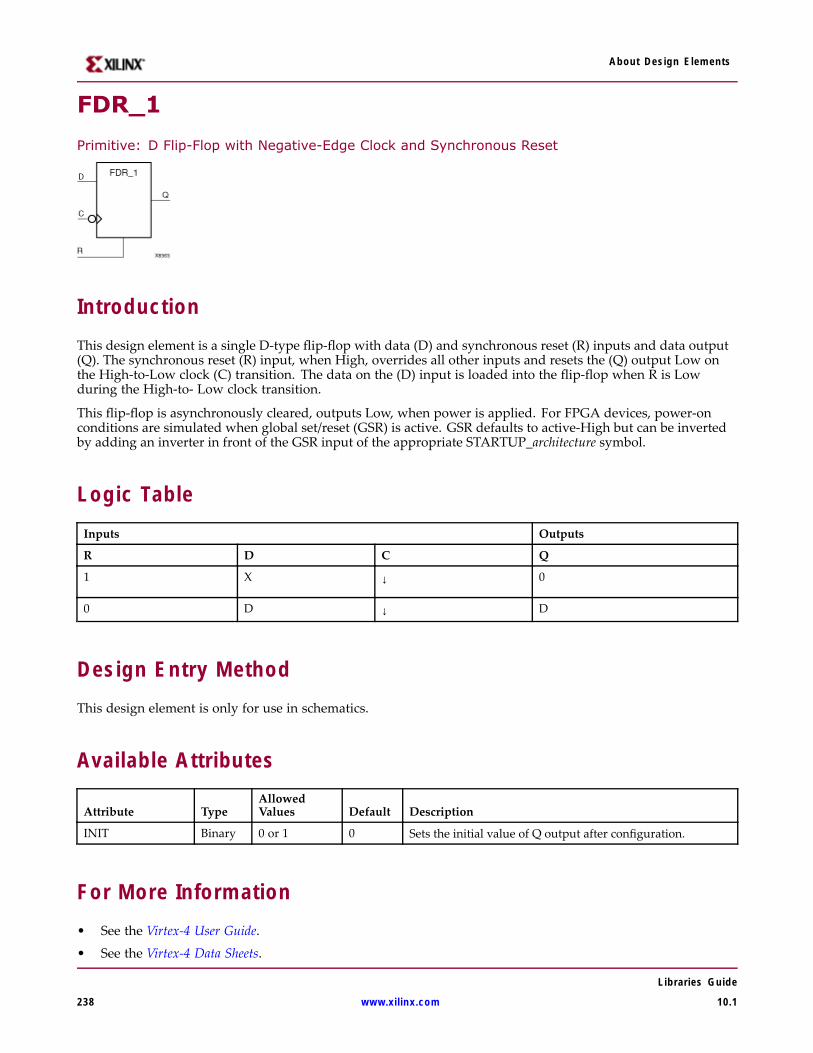
About Design Elements
FDR_1
Primitive: D Flip-Flop with Negative-Edge Clock and Synchronous Reset
IntroductionThis design element is a single D-type flip-flop with data (D) and synchronous reset (R) inputs and data output(Q). The synchronous reset (R) input, when High, overrides all other inputs and resets the (Q) output Low onthe High-to-Low clock (C) transition. The data on the (D) input is loaded into the flip-flop when R is Lowduring the High-to- Low clock transition.
This flip-flop is asynchronously cleared, outputs Low, when power is applied. For FPGA devices, power-onconditions are simulated when global set/reset (GSR) is active. GSR defaults to active-High but can be invertedby adding an inverter in front of the GSR input of the appropriate STARTUP_architecture symbol.
Logic TableInputs Outputs
R D C Q
1 X ↓ 0
0 D ↓ D
Design Entry MethodThis design element is only for use in schematics.
Available Attributes
Attribute TypeAllowedValues Default Description
INIT Binary 0 or 1 0 Sets the initial value of Q output after configuration.
For More Information• See the Virtex-4 User Guide.
• See the Virtex-4 Data Sheets.
Libraries Guide
238 www.xilinx.com 10.1
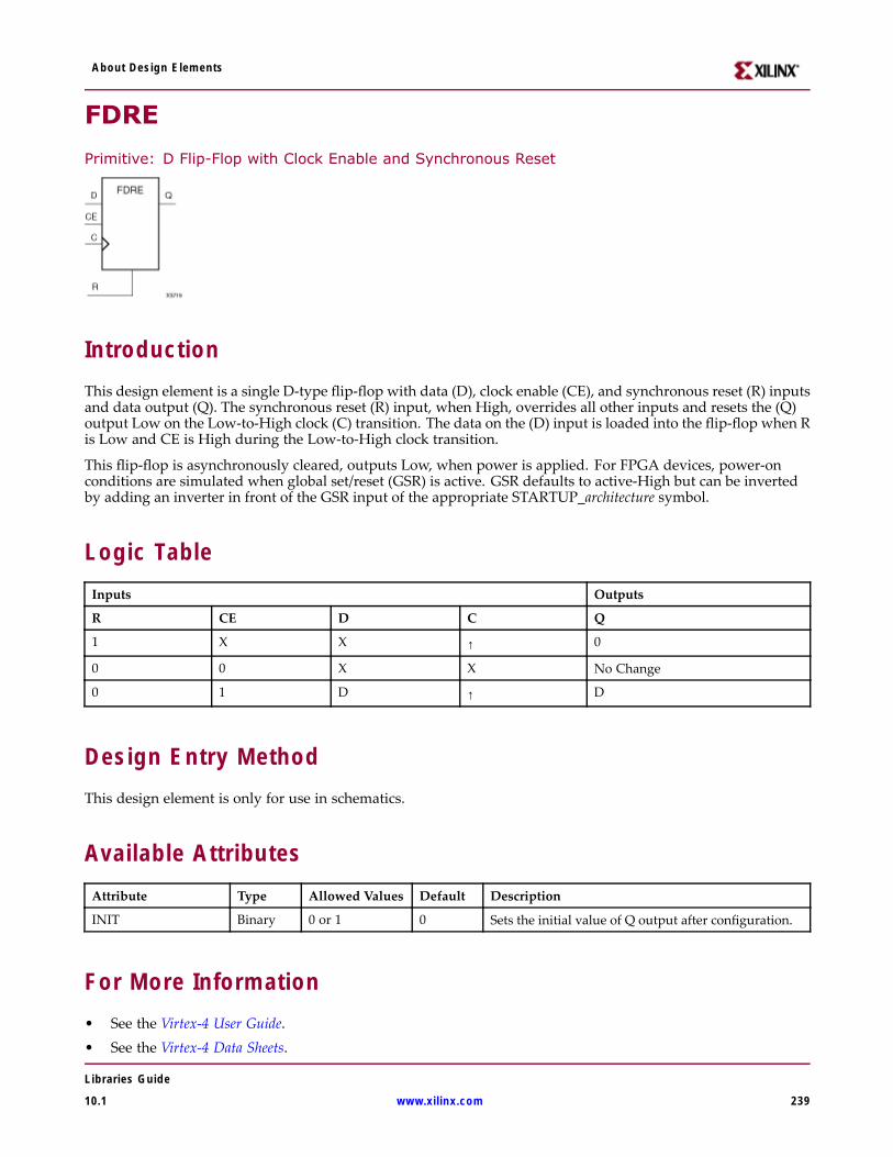
About Design Elements
FDRE
Primitive: D Flip-Flop with Clock Enable and Synchronous Reset
IntroductionThis design element is a single D-type flip-flop with data (D), clock enable (CE), and synchronous reset (R) inputsand data output (Q). The synchronous reset (R) input, when High, overrides all other inputs and resets the (Q)output Low on the Low-to-High clock (C) transition. The data on the (D) input is loaded into the flip-flop when Ris Low and CE is High during the Low-to-High clock transition.
This flip-flop is asynchronously cleared, outputs Low, when power is applied. For FPGA devices, power-onconditions are simulated when global set/reset (GSR) is active. GSR defaults to active-High but can be invertedby adding an inverter in front of the GSR input of the appropriate STARTUP_architecture symbol.
Logic TableInputs Outputs
R CE D C Q
1 X X ↑ 0
0 0 X X No Change
0 1 D ↑ D
Design Entry MethodThis design element is only for use in schematics.
Available AttributesAttribute Type Allowed Values Default Description
INIT Binary 0 or 1 0 Sets the initial value of Q output after configuration.
For More Information• See the Virtex-4 User Guide.• See the Virtex-4 Data Sheets.
Libraries Guide
10.1 www.xilinx.com 239
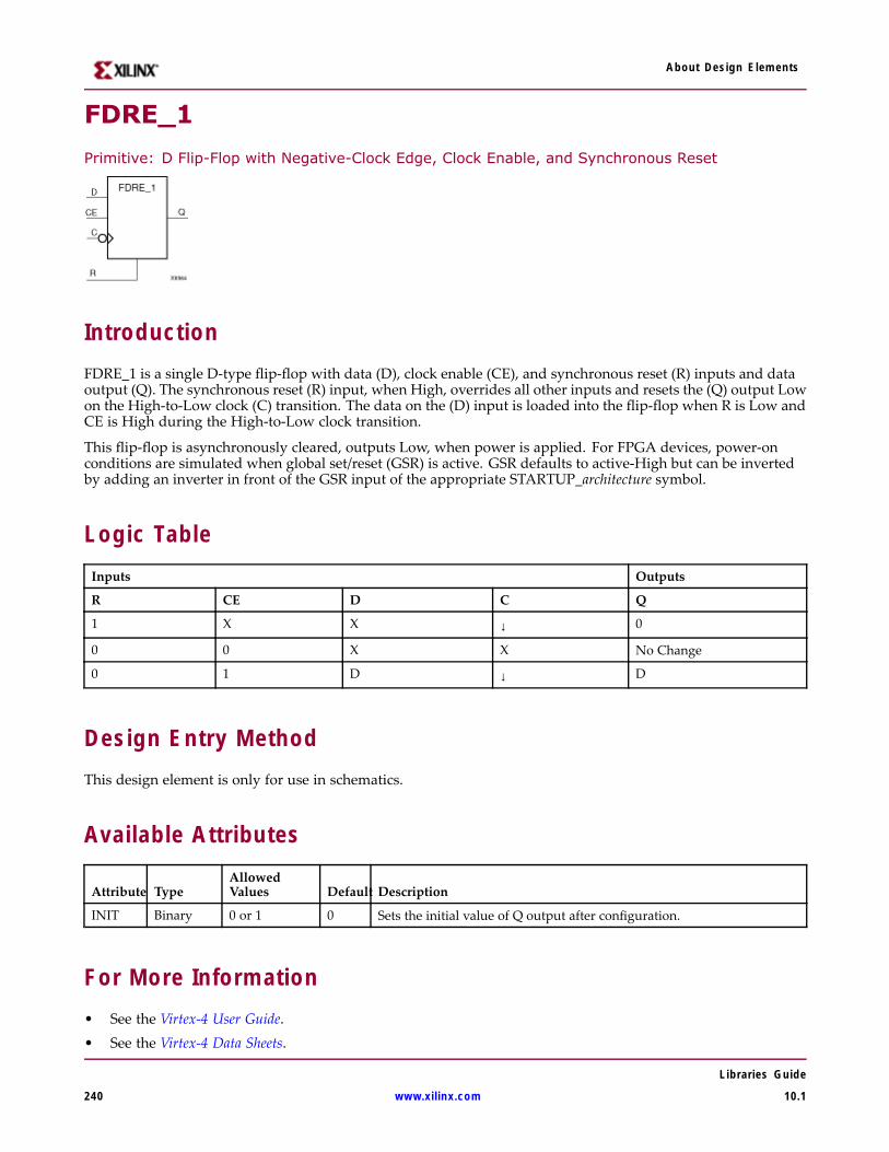
About Design Elements
FDRE_1
Primitive: D Flip-Flop with Negative-Clock Edge, Clock Enable, and Synchronous Reset
IntroductionFDRE_1 is a single D-type flip-flop with data (D), clock enable (CE), and synchronous reset (R) inputs and dataoutput (Q). The synchronous reset (R) input, when High, overrides all other inputs and resets the (Q) output Lowon the High-to-Low clock (C) transition. The data on the (D) input is loaded into the flip-flop when R is Low andCE is High during the High-to-Low clock transition.
This flip-flop is asynchronously cleared, outputs Low, when power is applied. For FPGA devices, power-onconditions are simulated when global set/reset (GSR) is active. GSR defaults to active-High but can be invertedby adding an inverter in front of the GSR input of the appropriate STARTUP_architecture symbol.
Logic TableInputs Outputs
R CE D C Q
1 X X ↓ 0
0 0 X X No Change
0 1 D ↓ D
Design Entry MethodThis design element is only for use in schematics.
Available Attributes
Attribute TypeAllowedValues Default Description
INIT Binary 0 or 1 0 Sets the initial value of Q output after configuration.
For More Information• See the Virtex-4 User Guide.• See the Virtex-4 Data Sheets.
Libraries Guide
240 www.xilinx.com 10.1
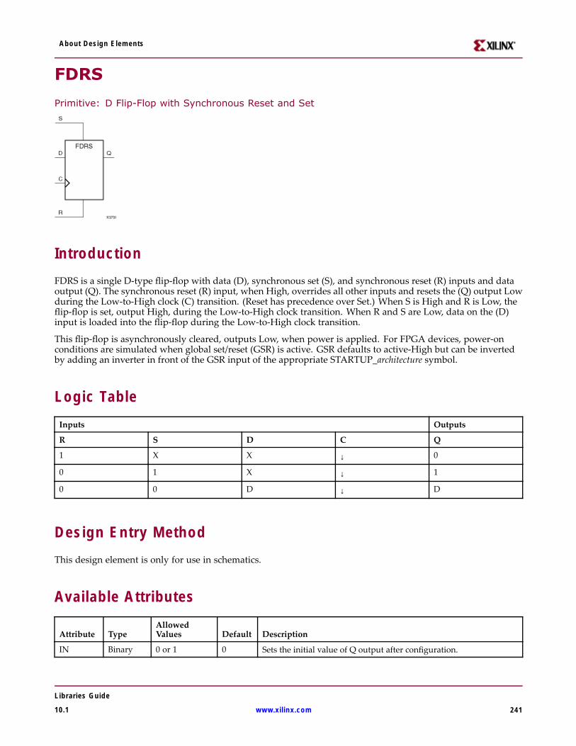
About Design Elements
FDRS
Primitive: D Flip-Flop with Synchronous Reset and Set
IntroductionFDRS is a single D-type flip-flop with data (D), synchronous set (S), and synchronous reset (R) inputs and dataoutput (Q). The synchronous reset (R) input, when High, overrides all other inputs and resets the (Q) output Lowduring the Low-to-High clock (C) transition. (Reset has precedence over Set.) When S is High and R is Low, theflip-flop is set, output High, during the Low-to-High clock transition. When R and S are Low, data on the (D)input is loaded into the flip-flop during the Low-to-High clock transition.
This flip-flop is asynchronously cleared, outputs Low, when power is applied. For FPGA devices, power-onconditions are simulated when global set/reset (GSR) is active. GSR defaults to active-High but can be invertedby adding an inverter in front of the GSR input of the appropriate STARTUP_architecture symbol.
Logic TableInputs Outputs
R S D C Q
1 X X ↓ 0
0 1 X ↓ 1
0 0 D ↓ D
Design Entry MethodThis design element is only for use in schematics.
Available Attributes
Attribute TypeAllowedValues Default Description
IN Binary 0 or 1 0 Sets the initial value of Q output after configuration.
Libraries Guide
10.1 www.xilinx.com 241

About Design Elements
For More Information• See the Virtex-4 User Guide.
• See the Virtex-4 Data Sheets.
Libraries Guide
242 www.xilinx.com 10.1
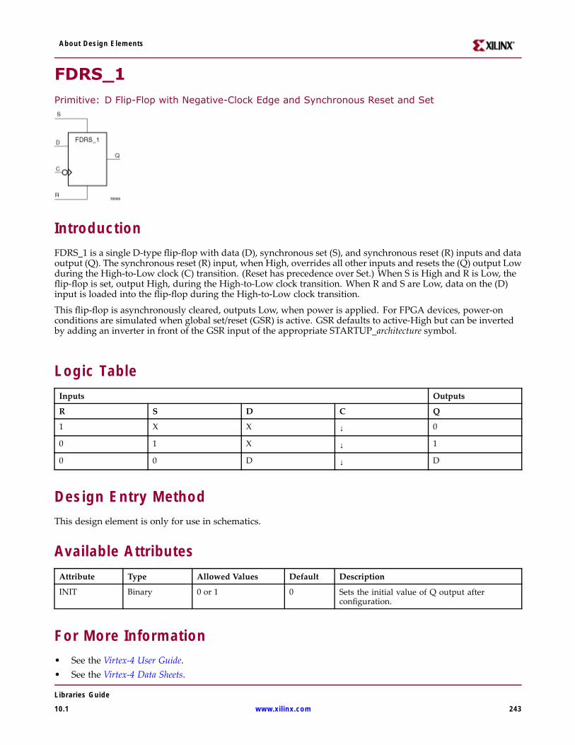
About Design Elements
FDRS_1Primitive: D Flip-Flop with Negative-Clock Edge and Synchronous Reset and Set
IntroductionFDRS_1 is a single D-type flip-flop with data (D), synchronous set (S), and synchronous reset (R) inputs and dataoutput (Q). The synchronous reset (R) input, when High, overrides all other inputs and resets the (Q) output Lowduring the High-to-Low clock (C) transition. (Reset has precedence over Set.) When S is High and R is Low, theflip-flop is set, output High, during the High-to-Low clock transition. When R and S are Low, data on the (D)input is loaded into the flip-flop during the High-to-Low clock transition.
This flip-flop is asynchronously cleared, outputs Low, when power is applied. For FPGA devices, power-onconditions are simulated when global set/reset (GSR) is active. GSR defaults to active-High but can be invertedby adding an inverter in front of the GSR input of the appropriate STARTUP_architecture symbol.
Logic TableInputs Outputs
R S D C Q
1 X X ↓ 0
0 1 X ↓ 1
0 0 D ↓ D
Design Entry MethodThis design element is only for use in schematics.
Available AttributesAttribute Type Allowed Values Default Description
INIT Binary 0 or 1 0 Sets the initial value of Q output afterconfiguration.
For More Information• See the Virtex-4 User Guide.• See the Virtex-4 Data Sheets.
Libraries Guide
10.1 www.xilinx.com 243
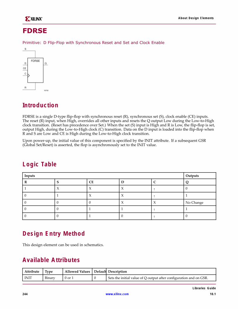
About Design Elements
FDRSE
Primitive: D Flip-Flop with Synchronous Reset and Set and Clock Enable
IntroductionFDRSE is a single D-type flip-flop with synchronous reset (R), synchronous set (S), clock enable (CE) inputs.The reset (R) input, when High, overrides all other inputs and resets the Q output Low during the Low-to-Highclock transition. (Reset has precedence over Set.) When the set (S) input is High and R is Low, the flip-flop is set,output High, during the Low-to-High clock (C) transition. Data on the D input is loaded into the flip-flop whenR and S are Low and CE is High during the Low-to-High clock transition.
Upon power-up, the initial value of this component is specified by the INIT attribute. If a subsequent GSR(Global Set/Reset) is asserted, the flop is asynchronously set to the INIT value.
Logic TableInputs Outputs
R S CE D C Q
1 X X X ↑ 0
0 1 X X ↑ 1
0 0 0 X X No Change
0 0 1 1 ↑ 1
0 0 1 0 ↑ 0
Design Entry MethodThis design element can be used in schematics.
Available AttributesAttribute Type Allowed Values Default Description
INIT Binary 0 or 1 0 Sets the initial value of Q output after configuration and on GSR.
Libraries Guide
244 www.xilinx.com 10.1

About Design Elements
For More Information• See the Virtex-4 User Guide.
• See the Virtex-4 Data Sheets.
Libraries Guide
10.1 www.xilinx.com 245
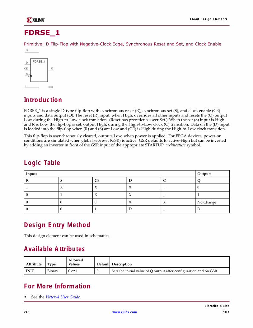
About Design Elements
FDRSE_1Primitive: D Flip-Flop with Negative-Clock Edge, Synchronous Reset and Set, and Clock Enable
IntroductionFDRSE_1 is a single D-type flip-flop with synchronous reset (R), synchronous set (S), and clock enable (CE)inputs and data output (Q). The reset (R) input, when High, overrides all other inputs and resets the (Q) outputLow during the High-to-Low clock transition. (Reset has precedence over Set.) When the set (S) input is Highand R is Low, the flip-flop is set, output High, during the High-to-Low clock (C) transition. Data on the (D) inputis loaded into the flip-flop when (R) and (S) are Low and (CE) is High during the High-to-Low clock transition.
This flip-flop is asynchronously cleared, outputs Low, when power is applied. For FPGA devices, power-onconditions are simulated when global set/reset (GSR) is active. GSR defaults to active-High but can be invertedby adding an inverter in front of the GSR input of the appropriate STARTUP_architecture symbol.
Logic TableInputs Outputs
R S CE D C Q
1 X X X ↓ 0
0 1 X X ↓ 1
0 0 0 X X No Change
0 0 1 D ↓ D
Design Entry MethodThis design element can be used in schematics.
Available Attributes
Attribute TypeAllowedValues Default Description
INIT Binary 0 or 1 0 Sets the initial value of Q output after configuration and on GSR.
For More Information• See the Virtex-4 User Guide.
Libraries Guide
246 www.xilinx.com 10.1

About Design Elements
• See the Virtex-4 Data Sheets.
Libraries Guide
10.1 www.xilinx.com 247
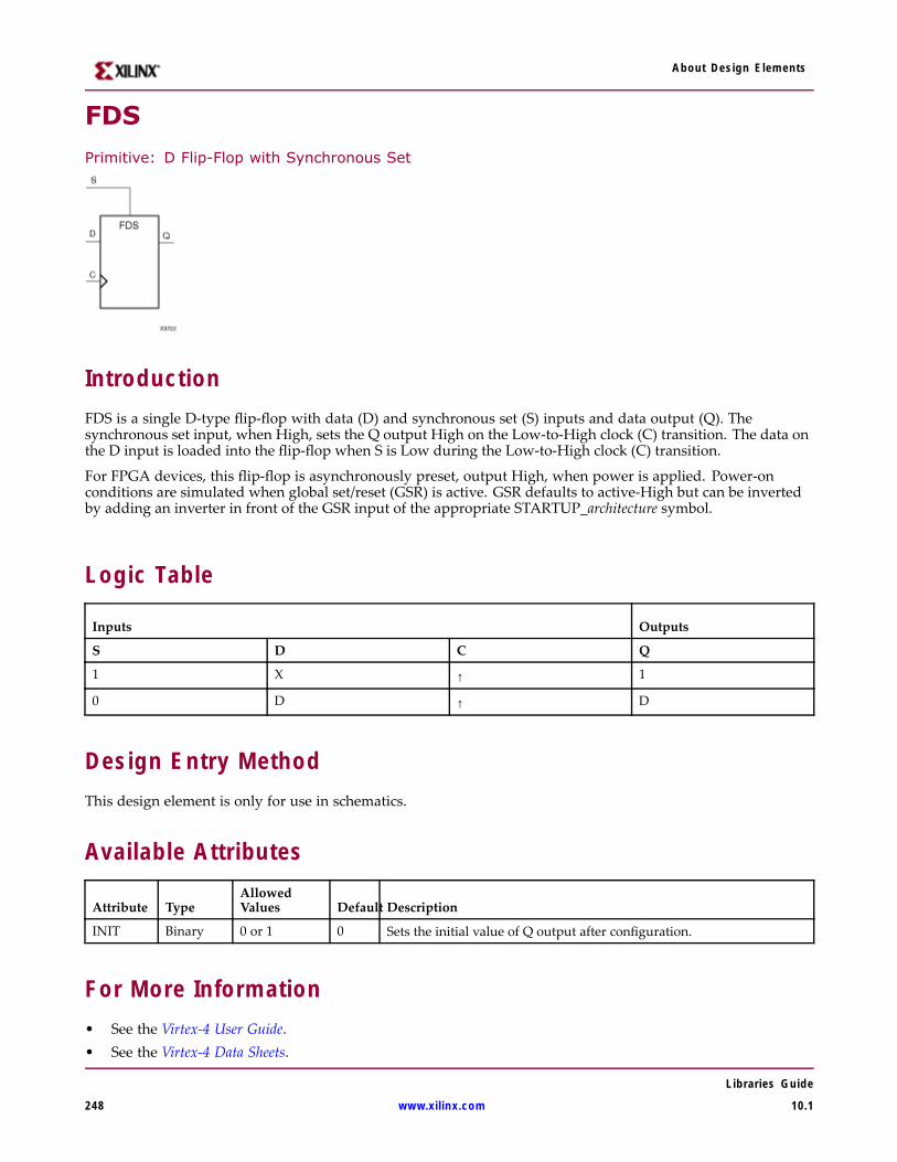
About Design Elements
FDS
Primitive: D Flip-Flop with Synchronous Set
IntroductionFDS is a single D-type flip-flop with data (D) and synchronous set (S) inputs and data output (Q). Thesynchronous set input, when High, sets the Q output High on the Low-to-High clock (C) transition. The data onthe D input is loaded into the flip-flop when S is Low during the Low-to-High clock (C) transition.
For FPGA devices, this flip-flop is asynchronously preset, output High, when power is applied. Power-onconditions are simulated when global set/reset (GSR) is active. GSR defaults to active-High but can be invertedby adding an inverter in front of the GSR input of the appropriate STARTUP_architecture symbol.
Logic Table
Inputs Outputs
S D C Q
1 X ↑ 1
0 D ↑ D
Design Entry MethodThis design element is only for use in schematics.
Available Attributes
Attribute TypeAllowedValues Default Description
INIT Binary 0 or 1 0 Sets the initial value of Q output after configuration.
For More Information• See the Virtex-4 User Guide.• See the Virtex-4 Data Sheets.
Libraries Guide
248 www.xilinx.com 10.1
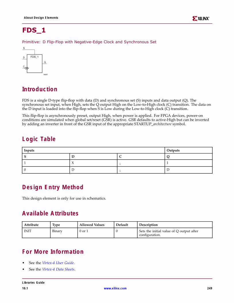
About Design Elements
FDS_1
Primitive: D Flip-Flop with Negative-Edge Clock and Synchronous Set
IntroductionFDS is a single D-type flip-flop with data (D) and synchronous set (S) inputs and data output (Q). Thesynchronous set input, when High, sets the Q output High on the Low-to-High clock (C) transition. The data onthe D input is loaded into the flip-flop when S is Low during the Low-to-High clock (C) transition.
This flip-flop is asynchronously preset, output High, when power is applied. For FPGA devices, power-onconditions are simulated when global set/reset (GSR) is active. GSR defaults to active-High but can be invertedby adding an inverter in front of the GSR input of the appropriate STARTUP_architecture symbol.
Logic TableInputs Outputs
S D C Q
1 X ↓ 1
0 D ↓ D
Design Entry MethodThis design element is only for use in schematics.
Available AttributesAttribute Type Allowed Values Default Description
INIT Binary 0 or 1 0 Sets the initial value of Q output afterconfiguration.
For More Information• See the Virtex-4 User Guide.
• See the Virtex-4 Data Sheets.
Libraries Guide
10.1 www.xilinx.com 249
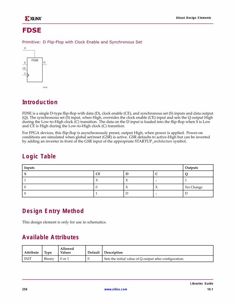
About Design Elements
FDSE
Primitive: D Flip-Flop with Clock Enable and Synchronous Set
IntroductionFDSE is a single D-type flip-flop with data (D), clock enable (CE), and synchronous set (S) inputs and data output(Q). The synchronous set (S) input, when High, overrides the clock enable (CE) input and sets the Q output Highduring the Low-to-High clock (C) transition. The data on the D input is loaded into the flip-flop when S is Lowand CE is High during the Low-to-High clock (C) transition.
For FPGA devices, this flip-flop is asynchronously preset, output High, when power is applied. Power-onconditions are simulated when global set/reset (GSR) is active. GSR defaults to active-High but can be invertedby adding an inverter in front of the GSR input of the appropriate STARTUP_architecture symbol.
Logic TableInputs Outputs
S CE D C Q
1 X X ↑ 1
0 0 X X No Change
0 1 D ↑ D
Design Entry MethodThis design element is only for use in schematics.
Available Attributes
Attribute TypeAllowedValues Default Description
INIT Binary 0 or 1 0 Sets the initial value of Q output after configuration.
Libraries Guide
250 www.xilinx.com 10.1

About Design Elements
For More Information• See the Virtex-4 User Guide.
• See the Virtex-4 Data Sheets.
Libraries Guide
10.1 www.xilinx.com 251

About Design Elements
FDSE_1
Primitive: D Flip-Flop with Negative-Edge Clock, Clock Enable, and Synchronous Set
IntroductionFDSE_1 is a single D-type flip-flop with data (D), clock enable (CE), and synchronous set (S) inputs and dataoutput (Q). The synchronous set (S) input, when High, overrides the clock enable (CE) input and sets the Qoutput High during the High-to-Low clock (C) transition. The data on the D input is loaded into the flip-flopwhen S is Low and CE is High during the High-to-Low clock (C) transition.
This flip-flop is asynchronously preset, output High, when power is applied. For FPGA devices, power-onconditions are simulated when global set/reset (GSR) is active. GSR defaults to active-High but can be invertedby adding an inverter in front of the GSR input of the appropriate STARTUP_architecture symbol.
Logic TableInputs Outputs
S CE D C Q
1 X X ↓ 1
0 0 X X No Change
0 1 D ↓ D
Design Entry MethodThis design element is only for use in schematics.
Available Attributes
Attribute TypeAllowedValues Default Description
INIT Binary 0 or 1 0 Sets the initial value of Q output after configuration.
For More Information• See the Virtex-4 User Guide.• See the Virtex-4 Data Sheets.
Libraries Guide
252 www.xilinx.com 10.1
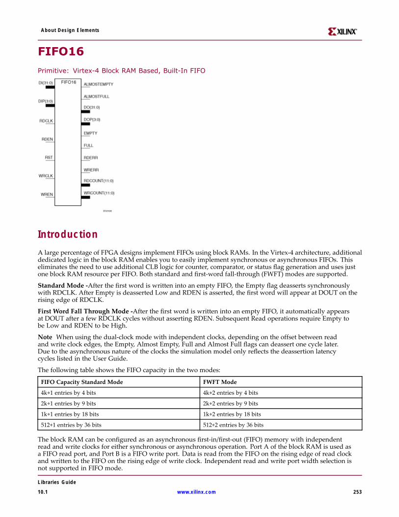
About Design Elements
FIFO16
Primitive: Virtex-4 Block RAM Based, Built-In FIFO
IntroductionA large percentage of FPGA designs implement FIFOs using block RAMs. In the Virtex-4 architecture, additionaldedicated logic in the block RAM enables you to easily implement synchronous or asynchronous FIFOs. Thiseliminates the need to use additional CLB logic for counter, comparator, or status flag generation and uses justone block RAM resource per FIFO. Both standard and first-word fall-through (FWFT) modes are supported.
Standard Mode -After the first word is written into an empty FIFO, the Empty flag deasserts synchronouslywith RDCLK. After Empty is deasserted Low and RDEN is asserted, the first word will appear at DOUT on therising edge of RDCLK.
First Word Fall Through Mode -After the first word is written into an empty FIFO, it automatically appearsat DOUT after a few RDCLK cycles without asserting RDEN. Subsequent Read operations require Empty tobe Low and RDEN to be High.
Note When using the dual-clock mode with independent clocks, depending on the offset between readand write clock edges, the Empty, Almost Empty, Full and Almost Full flags can deassert one cycle later.Due to the asynchronous nature of the clocks the simulation model only reflects the deassertion latencycycles listed in the User Guide.
The following table shows the FIFO capacity in the two modes:
FIFO Capacity Standard Mode FWFT Mode
4k+1 entries by 4 bits 4k+2 entries by 4 bits
2k+1 entries by 9 bits 2k+2 entries by 9 bits
1k+1 entries by 18 bits 1k+2 entries by 18 bits
512+1 entries by 36 bits 512+2 entries by 36 bits
The block RAM can be configured as an asynchronous first-in/first-out (FIFO) memory with independentread and write clocks for either synchronous or asynchronous operation. Port A of the block RAM is used asa FIFO read port, and Port B is a FIFO write port. Data is read from the FIFO on the rising edge of read clockand written to the FIFO on the rising edge of write clock. Independent read and write port width selection isnot supported in FIFO mode.
Libraries Guide
10.1 www.xilinx.com 253
About Design Elements
The available status flags are:• Full (FULL) - Synchronous to WRCLK. The Full flag is asserted when there are no more available entries in
the FIFO queue. When the FIFO is full, the write pointer will be frozen. This ensures the read and writepointers point to the same entry and no overflow will occur. The Full flag is registered at the output andtakes one write cycle to assert. The Full flag is deasserted three clock cycles after the last entry is read, andit is synchronous to WRCLK.
• Empty (EMPTY) - Synchronous to RDCLK.• Almost Full (AFULL) - Synchronous to WRCLK. The Almost Full flag is set when the FIFO has fewer than
the number of available empty spaces specified by the ALMOST_FULL_OFFSET value. The Almost Fullflag warns you to stop writing. It deasserts when the number of empty spaces in the FIFO is greater thanthe ALMOST_FULL_OFFSET value, and is synchronous to WRCLK.
• Almost Empty (AEMPTY) - Synchronous to RDCLK.• Write Count (WRCOUNT) - Synchronous to WRCLK.• Write Error (WRERR) - Synchronous to WRCLK. Once the Full flag has been asserted, any further write
attempts will trigger the Write Error flag. The Write Error flag is deasserted when Write Enable or Full isdeasserted Low. This signal is synchronous to WRCLK.
• Read Count (RDCOUNT) - Synchronous to RDCLK.• Read Error (RDERR) - Synchronous to RDCLK.
Port DescriptionsPort Direction Function
DI Input Data input
DIP Input Parity-bit input
WREN Input Write enable. WhenWREN = 1, data will be written to memory.When WREN = 0, write is disabled.
WRCLK Input Clock for write domain operation.
RDEN Input Read enable. When RDEN = 1, data will be read to outputregister. When RDEN = 0, read is disabled.
RDCLK Input Clock for read domain operation.
RESET Input Asynchronous reset of all FIFO functions, flags, and pointers.
DO Output Data output, synchronous to RDCLK
DOP Output Parity-bit output, synchronous to RDCLK
FULL Output All entries in FIFO memory are filled.
ALMOSTFULL Output Almost all entries in FIFO memory have been filled.Synchronous to WRCLK. The value is configurable by you.
EMPTY Output FIFO is empty. No additional read can be performed.Synchronous to RDCLK.
ALMOSTEMPTY Output Almost all valid entries in FIFO are read. Synchronous withRDCLK. The value is configurable by you.
RDCOUNT Output The FIFO data read pointer. It is synchronous with RDCLK.The value will wrap around if the maximum read pointer valuehas been reached.
WRCOUNT Output The FIFO data write pointer. It is synchronous with WRCLK.The value will wrap around if the maximum write pointervalue has been reached.
Libraries Guide
254 www.xilinx.com 10.1
About Design Elements
Port Direction Function
WRERR Output When the FIFO is full, any additional write operation generatesan error flag. Synchronous with WRCLK.
RDERR Output When the FIFO is empty, any additional read operationgenerates an error flag. Synchronous with RDCLK.
Design Entry MethodThis design element can be used in schematics.
Available AttributesAttribute Type Allowed Values Default Description
ALMOST_EMPTY_OFFSET
Hexadecimal Any 12-Bit Value All zeros Sets the almost empty threshold.
ALMOST_FULL_OFFSET
Hexadecimal Any 12-Bit Value All zeros Sets almost full threshold.
DATA_WIDTH Integer 4, 9, 18, 36 36 Sets data width to allowed value.
FIRST_WORD_FALL_THROUGH
Boolean FALSE, TRUE FALSE Sets the FIFO FWFT to "TRUE" or"FALSE."
For More Information• See the Virtex-4 User Guide.
• See the Virtex-4 Data Sheets.
Libraries Guide
10.1 www.xilinx.com 255
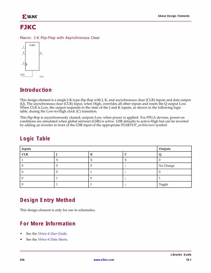
About Design Elements
FJKC
Macro: J-K Flip-Flop with Asynchronous Clear
IntroductionThis design element is a single J-K-type flip-flop with J, K, and asynchronous clear (CLR) inputs and data output(Q). The asynchronous clear (CLR) input, when High, overrides all other inputs and resets the Q output Low.When CLR is Low, the output responds to the state of the J and K inputs, as shown in the following logictable, during the Low-to-High clock (C) transition.
This flip-flop is asynchronously cleared, outputs Low, when power is applied. For FPGA devices, power-onconditions are simulated when global set/reset (GSR) is active. GSR defaults to active-High but can be invertedby adding an inverter in front of the GSR input of the appropriate STARTUP_architecture symbol.
Logic TableInputs Outputs
CLR J K C Q
1 X X X 0
0 0 0 ↑ No Change
0 0 1 ↑ 0
0 1 0 ↑ 1
0 1 1 ↑ Toggle
Design Entry MethodThis design element is only for use in schematics.
For More Information• See the Virtex-4 User Guide.
• See the Virtex-4 Data Sheets.
Libraries Guide
256 www.xilinx.com 10.1
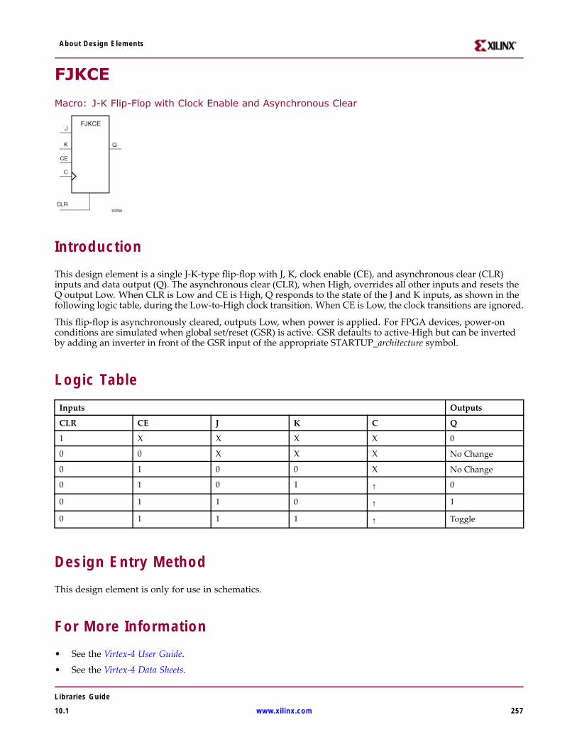
About Design Elements
FJKCE
Macro: J-K Flip-Flop with Clock Enable and Asynchronous Clear
IntroductionThis design element is a single J-K-type flip-flop with J, K, clock enable (CE), and asynchronous clear (CLR)inputs and data output (Q). The asynchronous clear (CLR), when High, overrides all other inputs and resets theQ output Low. When CLR is Low and CE is High, Q responds to the state of the J and K inputs, as shown in thefollowing logic table, during the Low-to-High clock transition. When CE is Low, the clock transitions are ignored.
This flip-flop is asynchronously cleared, outputs Low, when power is applied. For FPGA devices, power-onconditions are simulated when global set/reset (GSR) is active. GSR defaults to active-High but can be invertedby adding an inverter in front of the GSR input of the appropriate STARTUP_architecture symbol.
Logic TableInputs Outputs
CLR CE J K C Q
1 X X X X 0
0 0 X X X No Change
0 1 0 0 X No Change
0 1 0 1 ↑ 0
0 1 1 0 ↑ 1
0 1 1 1 ↑ Toggle
Design Entry MethodThis design element is only for use in schematics.
For More Information• See the Virtex-4 User Guide.
• See the Virtex-4 Data Sheets.
Libraries Guide
10.1 www.xilinx.com 257
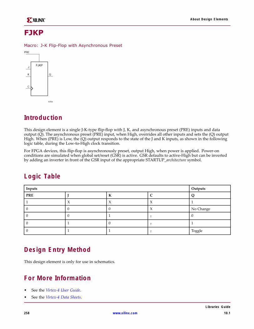
About Design Elements
FJKP
Macro: J-K Flip-Flop with Asynchronous Preset
IntroductionThis design element is a single J-K-type flip-flop with J, K, and asynchronous preset (PRE) inputs and dataoutput (Q). The asynchronous preset (PRE) input, when High, overrides all other inputs and sets the (Q) outputHigh. When (PRE) is Low, the (Q) output responds to the state of the J and K inputs, as shown in the followinglogic table, during the Low-to-High clock transition.
For FPGA devices, this flip-flop is asynchronously preset, output High, when power is applied. Power-onconditions are simulated when global set/reset (GSR) is active. GSR defaults to active-High but can be invertedby adding an inverter in front of the GSR input of the appropriate STARTUP_architecture symbol.
Logic TableInputs Outputs
PRE J K C Q
1 X X X 1
0 0 0 X No Change
0 0 1 ↑ 0
0 1 0 ↑ 1
0 1 1 ↑ Toggle
Design Entry MethodThis design element is only for use in schematics.
For More Information• See the Virtex-4 User Guide.
• See the Virtex-4 Data Sheets.
Libraries Guide
258 www.xilinx.com 10.1

About Design Elements
FJKPEMacro: J-K Flip-Flop with Clock Enable and Asynchronous Preset
IntroductionThis design element is a single J-K-type flip-flop with J, K, clock enable (CE), and asynchronous preset (PRE)inputs and data output (Q). The asynchronous preset (PRE), when High, overrides all other inputs and sets the(Q) output High. When (PRE) is Low and (CE) is High, the (Q) output responds to the state of the J and Kinputs, as shown in the logic table, during the Low-to-High clock (C) transition. When (CE) is Low, clocktransitions are ignored.
For FPGA devices, this flip-flop is asynchronously preset, output High, when power is applied. Power-onconditions are simulated when global set/reset (GSR) is active. GSR defaults to active-High but can be invertedby adding an inverter in front of the GSR input of the appropriate STARTUP_architecture symbol.
Logic TableInputs Outputs
PRE CE J K C Q
1 X X X X 1
0 0 X X X No Change
0 1 0 0 X No Change
0 1 0 1 ↑ 0
0 1 1 0 ↑ 1
0 1 1 1 ↑ Toggle
Design Entry MethodThis design element is only for use in schematics.
For More Information• See the Virtex-4 User Guide.• See the Virtex-4 Data Sheets.
Libraries Guide
10.1 www.xilinx.com 259
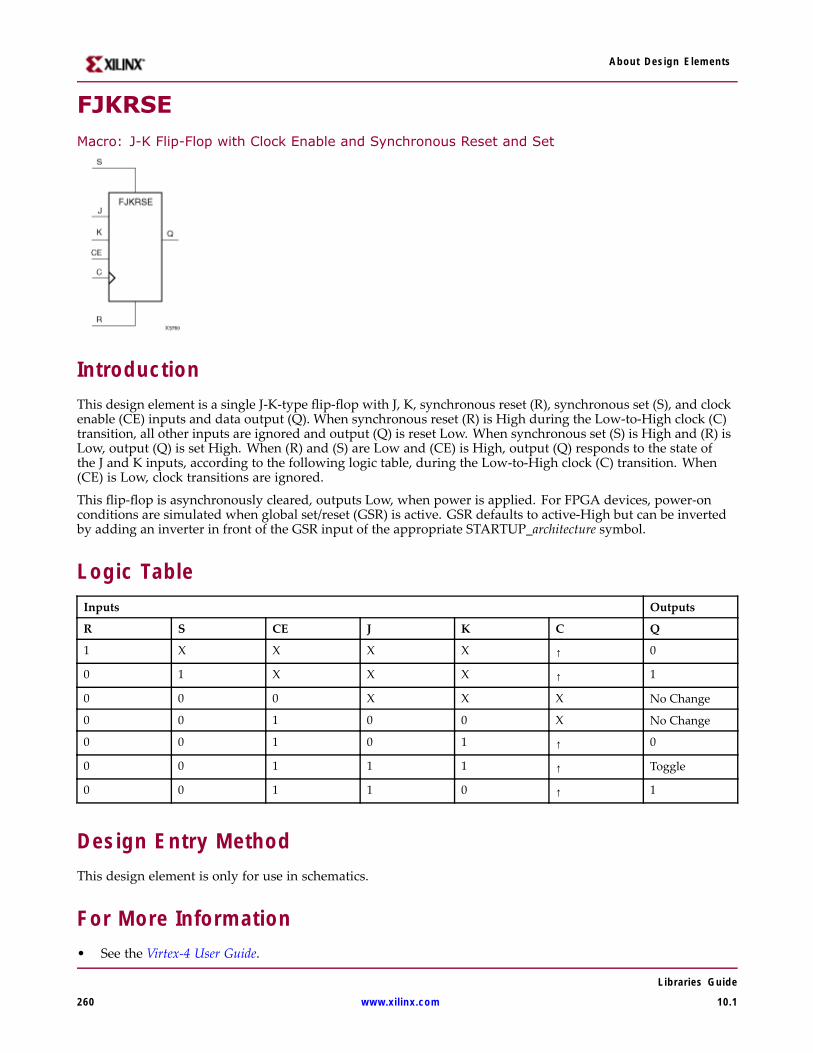
About Design Elements
FJKRSEMacro: J-K Flip-Flop with Clock Enable and Synchronous Reset and Set
IntroductionThis design element is a single J-K-type flip-flop with J, K, synchronous reset (R), synchronous set (S), and clockenable (CE) inputs and data output (Q). When synchronous reset (R) is High during the Low-to-High clock (C)transition, all other inputs are ignored and output (Q) is reset Low. When synchronous set (S) is High and (R) isLow, output (Q) is set High. When (R) and (S) are Low and (CE) is High, output (Q) responds to the state ofthe J and K inputs, according to the following logic table, during the Low-to-High clock (C) transition. When(CE) is Low, clock transitions are ignored.
This flip-flop is asynchronously cleared, outputs Low, when power is applied. For FPGA devices, power-onconditions are simulated when global set/reset (GSR) is active. GSR defaults to active-High but can be invertedby adding an inverter in front of the GSR input of the appropriate STARTUP_architecture symbol.
Logic TableInputs Outputs
R S CE J K C Q
1 X X X X ↑ 0
0 1 X X X ↑ 1
0 0 0 X X X No Change
0 0 1 0 0 X No Change
0 0 1 0 1 ↑ 0
0 0 1 1 1 ↑ Toggle
0 0 1 1 0 ↑ 1
Design Entry MethodThis design element is only for use in schematics.
For More Information• See the Virtex-4 User Guide.
Libraries Guide
260 www.xilinx.com 10.1

About Design Elements
• See the Virtex-4 Data Sheets.
Libraries Guide
10.1 www.xilinx.com 261
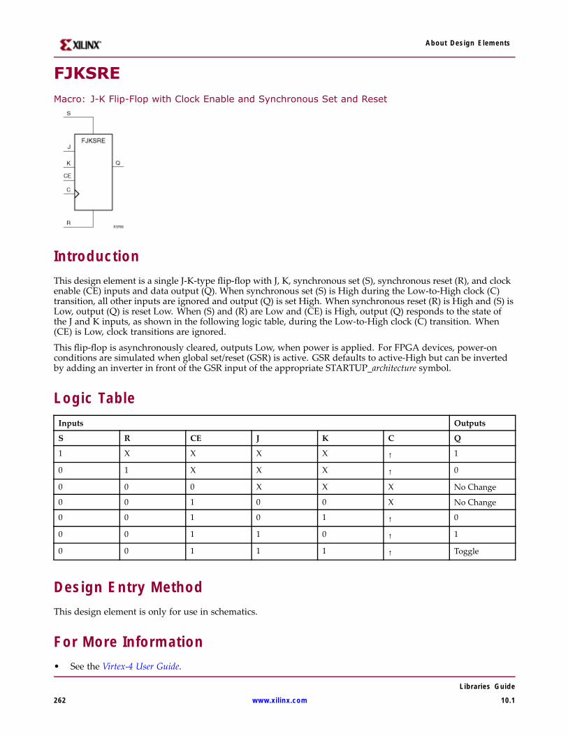
About Design Elements
FJKSREMacro: J-K Flip-Flop with Clock Enable and Synchronous Set and Reset
IntroductionThis design element is a single J-K-type flip-flop with J, K, synchronous set (S), synchronous reset (R), and clockenable (CE) inputs and data output (Q). When synchronous set (S) is High during the Low-to-High clock (C)transition, all other inputs are ignored and output (Q) is set High. When synchronous reset (R) is High and (S) isLow, output (Q) is reset Low. When (S) and (R) are Low and (CE) is High, output (Q) responds to the state ofthe J and K inputs, as shown in the following logic table, during the Low-to-High clock (C) transition. When(CE) is Low, clock transitions are ignored.
This flip-flop is asynchronously cleared, outputs Low, when power is applied. For FPGA devices, power-onconditions are simulated when global set/reset (GSR) is active. GSR defaults to active-High but can be invertedby adding an inverter in front of the GSR input of the appropriate STARTUP_architecture symbol.
Logic TableInputs Outputs
S R CE J K C Q
1 X X X X ↑ 1
0 1 X X X ↑ 0
0 0 0 X X X No Change
0 0 1 0 0 X No Change
0 0 1 0 1 ↑ 0
0 0 1 1 0 ↑ 1
0 0 1 1 1 ↑ Toggle
Design Entry MethodThis design element is only for use in schematics.
For More Information• See the Virtex-4 User Guide.
Libraries Guide
262 www.xilinx.com 10.1

About Design Elements
• See the Virtex-4 Data Sheets.
Libraries Guide
10.1 www.xilinx.com 263
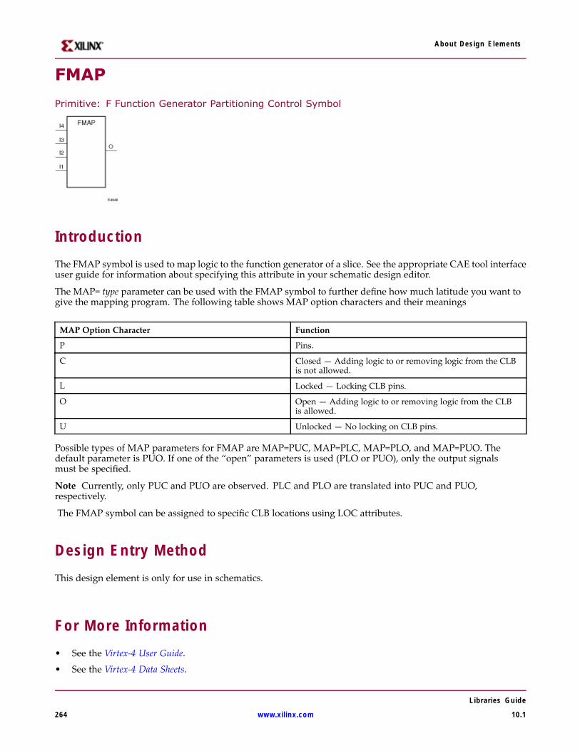
About Design Elements
FMAP
Primitive: F Function Generator Partitioning Control Symbol
IntroductionThe FMAP symbol is used to map logic to the function generator of a slice. See the appropriate CAE tool interfaceuser guide for information about specifying this attribute in your schematic design editor.
The MAP= type parameter can be used with the FMAP symbol to further define how much latitude you want togive the mapping program. The following table shows MAP option characters and their meanings
MAP Option Character Function
P Pins.
C Closed — Adding logic to or removing logic from the CLBis not allowed.
L Locked — Locking CLB pins.
O Open — Adding logic to or removing logic from the CLBis allowed.
U Unlocked — No locking on CLB pins.
Possible types of MAP parameters for FMAP are MAP=PUC, MAP=PLC, MAP=PLO, and MAP=PUO. Thedefault parameter is PUO. If one of the “open” parameters is used (PLO or PUO), only the output signalsmust be specified.
Note Currently, only PUC and PUO are observed. PLC and PLO are translated into PUC and PUO,respectively.
The FMAP symbol can be assigned to specific CLB locations using LOC attributes.
Design Entry MethodThis design element is only for use in schematics.
For More Information• See the Virtex-4 User Guide.
• See the Virtex-4 Data Sheets.
Libraries Guide
264 www.xilinx.com 10.1

About Design Elements
FRAME_ECC_VIRTEX4Primitive: Reads a Single, Virtex-4 Configuration Frame and Computes a Hamming, Single-ErrorCorrection, Double-Error Detection Syndrome
IntroductionThis design element reads a single Virtex-4 configuration frame of 1312-bits, 32-bits at a time. It will thencompute a Hamming single error correction, double error detection "syndrome." This identifies the single framebit (if any), which is in error and should be corrected. It also indicates the presence of two bit errors, whichcannot be corrected. Note that the FRAME_ECC_VIRTEX4 primitive does not repair changed bits.
Port Descriptions
Port Direction Width Function
ERROR Output 1 Error Output. Indicates whether or not an error exists.
SYNDROME Output 12 Indicates the location of the erroneous bit. Provides the bitlocation of the error and whether zero, one, or two erroneousbits are present.
SYNDROMEVALID Output 1 When value is High, indicates the presence of zero, one or two biterrors in the frame. When asserted HIGH, SYNDROMEVALIDindicates that the end of a frame readback.
Design Entry MethodThis design element can be used in schematics.
Syndrome Value and Corresponding Error StatusSyndrome bit 11 Syndrome bit 10 to 0 Error Status
0 All 0s No bit errors
0 Not equal to 0 One bit error, and syndrome valueidentifies the position of the erroneousbit
1 All 0s Two bit errors, not correctable
Note SYNDROME_VALID must be HIGH for the values on the table above to be useful.
For More Information• See the Virtex-4 User Guide.
Libraries Guide
10.1 www.xilinx.com 265

About Design Elements
• See the Virtex-4 Data Sheets.
Libraries Guide
266 www.xilinx.com 10.1
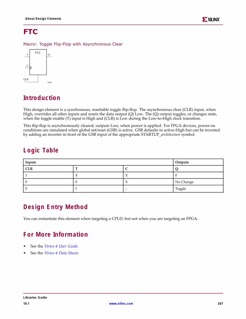
About Design Elements
FTC
Macro: Toggle Flip-Flop with Asynchronous Clear
IntroductionThis design element is a synchronous, resettable toggle flip-flop. The asynchronous clear (CLR) input, whenHigh, overrides all other inputs and resets the data output (Q) Low. The (Q) output toggles, or changes state,when the toggle enable (T) input is High and (CLR) is Low during the Low-to-High clock transition.
This flip-flop is asynchronously cleared, outputs Low, when power is applied. For FPGA devices, power-onconditions are simulated when global set/reset (GSR) is active. GSR defaults to active-High but can be invertedby adding an inverter in front of the GSR input of the appropriate STARTUP_architecture symbol.
Logic TableInputs Outputs
CLR T C Q
1 X X 0
0 0 X No Change
0 1 ↑ Toggle
Design Entry MethodYou can instantiate this element when targeting a CPLD, but not when you are targeting an FPGA.
For More Information• See the Virtex-4 User Guide.
• See the Virtex-4 Data Sheets.
Libraries Guide
10.1 www.xilinx.com 267
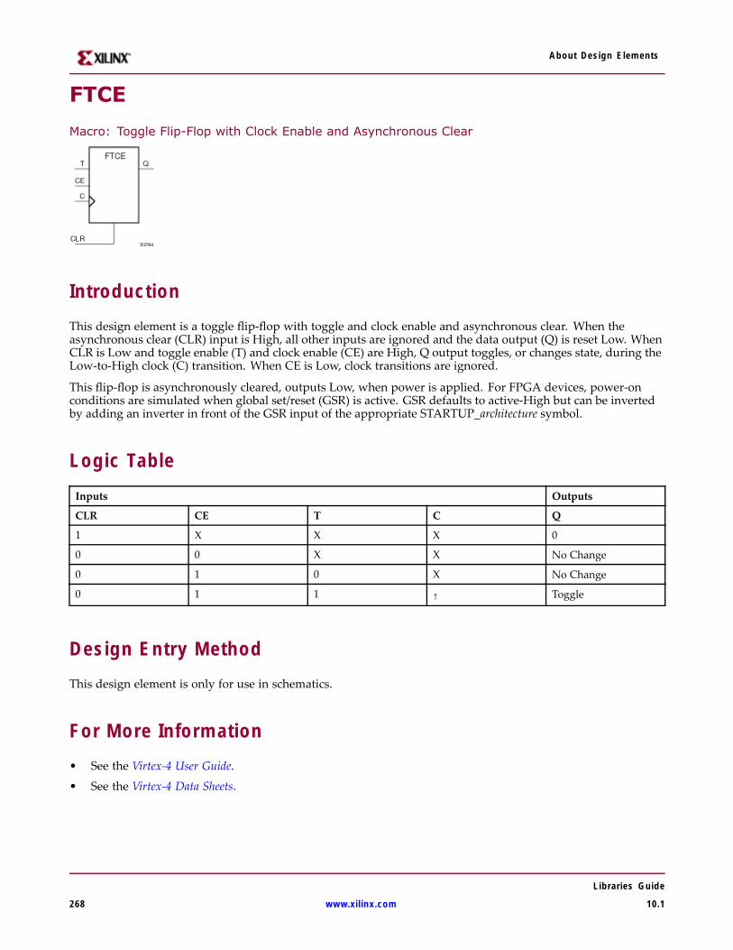
About Design Elements
FTCE
Macro: Toggle Flip-Flop with Clock Enable and Asynchronous Clear
IntroductionThis design element is a toggle flip-flop with toggle and clock enable and asynchronous clear. When theasynchronous clear (CLR) input is High, all other inputs are ignored and the data output (Q) is reset Low. WhenCLR is Low and toggle enable (T) and clock enable (CE) are High, Q output toggles, or changes state, during theLow-to-High clock (C) transition. When CE is Low, clock transitions are ignored.
This flip-flop is asynchronously cleared, outputs Low, when power is applied. For FPGA devices, power-onconditions are simulated when global set/reset (GSR) is active. GSR defaults to active-High but can be invertedby adding an inverter in front of the GSR input of the appropriate STARTUP_architecture symbol.
Logic TableInputs Outputs
CLR CE T C Q
1 X X X 0
0 0 X X No Change
0 1 0 X No Change
0 1 1 ↑ Toggle
Design Entry MethodThis design element is only for use in schematics.
For More Information• See the Virtex-4 User Guide.
• See the Virtex-4 Data Sheets.
Libraries Guide
268 www.xilinx.com 10.1
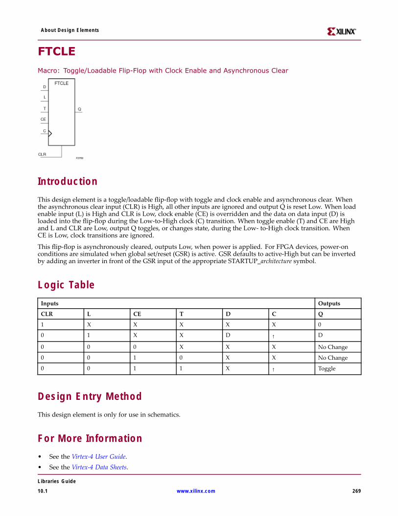
About Design Elements
FTCLE
Macro: Toggle/Loadable Flip-Flop with Clock Enable and Asynchronous Clear
IntroductionThis design element is a toggle/loadable flip-flop with toggle and clock enable and asynchronous clear. Whenthe asynchronous clear input (CLR) is High, all other inputs are ignored and output Q is reset Low. When loadenable input (L) is High and CLR is Low, clock enable (CE) is overridden and the data on data input (D) isloaded into the flip-flop during the Low-to-High clock (C) transition. When toggle enable (T) and CE are Highand L and CLR are Low, output Q toggles, or changes state, during the Low- to-High clock transition. WhenCE is Low, clock transitions are ignored.
This flip-flop is asynchronously cleared, outputs Low, when power is applied. For FPGA devices, power-onconditions are simulated when global set/reset (GSR) is active. GSR defaults to active-High but can be invertedby adding an inverter in front of the GSR input of the appropriate STARTUP_architecture symbol.
Logic TableInputs Outputs
CLR L CE T D C Q
1 X X X X X 0
0 1 X X D ↑ D
0 0 0 X X X No Change
0 0 1 0 X X No Change
0 0 1 1 X ↑ Toggle
Design Entry MethodThis design element is only for use in schematics.
For More Information• See the Virtex-4 User Guide.• See the Virtex-4 Data Sheets.
Libraries Guide
10.1 www.xilinx.com 269
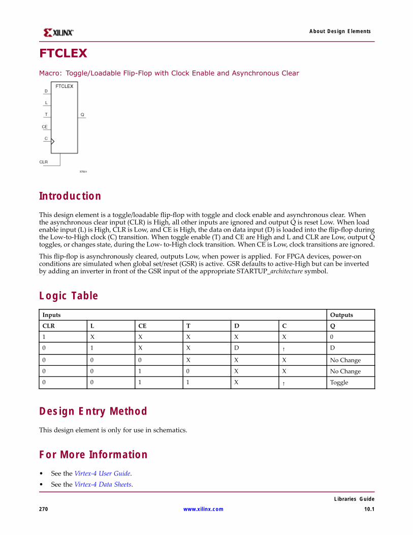
About Design Elements
FTCLEX
Macro: Toggle/Loadable Flip-Flop with Clock Enable and Asynchronous Clear
IntroductionThis design element is a toggle/loadable flip-flop with toggle and clock enable and asynchronous clear. Whenthe asynchronous clear input (CLR) is High, all other inputs are ignored and output Q is reset Low. When loadenable input (L) is High, CLR is Low, and CE is High, the data on data input (D) is loaded into the flip-flop duringthe Low-to-High clock (C) transition. When toggle enable (T) and CE are High and L and CLR are Low, output Qtoggles, or changes state, during the Low- to-High clock transition. When CE is Low, clock transitions are ignored.
This flip-flop is asynchronously cleared, outputs Low, when power is applied. For FPGA devices, power-onconditions are simulated when global set/reset (GSR) is active. GSR defaults to active-High but can be invertedby adding an inverter in front of the GSR input of the appropriate STARTUP_architecture symbol.
Logic TableInputs Outputs
CLR L CE T D C Q
1 X X X X X 0
0 1 X X D ↑ D
0 0 0 X X X No Change
0 0 1 0 X X No Change
0 0 1 1 X ↑ Toggle
Design Entry MethodThis design element is only for use in schematics.
For More Information• See the Virtex-4 User Guide.• See the Virtex-4 Data Sheets.
Libraries Guide
270 www.xilinx.com 10.1

About Design Elements
FTP
Macro: Toggle Flip-Flop with Asynchronous Preset
IntroductionThis design element is a toggle flip-flop with toggle enable and asynchronous preset. When the asynchronouspreset (PRE) input is High, all other inputs are ignored and output (Q) is set High. When toggle-enable input (T)is High and (PRE) is Low, output (Q) toggles, or changes state, during the Low-to-High clock (C) transition.
For FPGA devices, this flip-flop is asynchronously preset, output High, when power is applied. Power-onconditions are simulated when global set/reset (GSR) is active. GSR defaults to active-High but can be invertedby adding an inverter in front of the GSR input of the appropriate STARTUP_architecture symbol.
Logic TableInputs Outputs
PRE T C Q
1 X X 1
0 0 X No Change
0 1 ↑ Toggle
Design Entry MethodThis design element is only for use in schematics.
For More Information• See the Virtex-4 User Guide.
• See the Virtex-4 Data Sheets.
Libraries Guide
10.1 www.xilinx.com 271
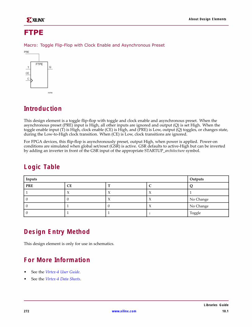
About Design Elements
FTPE
Macro: Toggle Flip-Flop with Clock Enable and Asynchronous Preset
IntroductionThis design element is a toggle flip-flop with toggle and clock enable and asynchronous preset. When theasynchronous preset (PRE) input is High, all other inputs are ignored and output (Q) is set High. When thetoggle enable input (T) is High, clock enable (CE) is High, and (PRE) is Low, output (Q) toggles, or changes state,during the Low-to-High clock transition. When (CE) is Low, clock transitions are ignored.
For FPGA devices, this flip-flop is asynchronously preset, output High, when power is applied. Power-onconditions are simulated when global set/reset (GSR) is active. GSR defaults to active-High but can be invertedby adding an inverter in front of the GSR input of the appropriate STARTUP_architecture symbol.
Logic TableInputs Outputs
PRE CE T C Q
1 X X X 1
0 0 X X No Change
0 1 0 X No Change
0 1 1 ↑ Toggle
Design Entry MethodThis design element is only for use in schematics.
For More Information• See the Virtex-4 User Guide.
• See the Virtex-4 Data Sheets.
Libraries Guide
272 www.xilinx.com 10.1
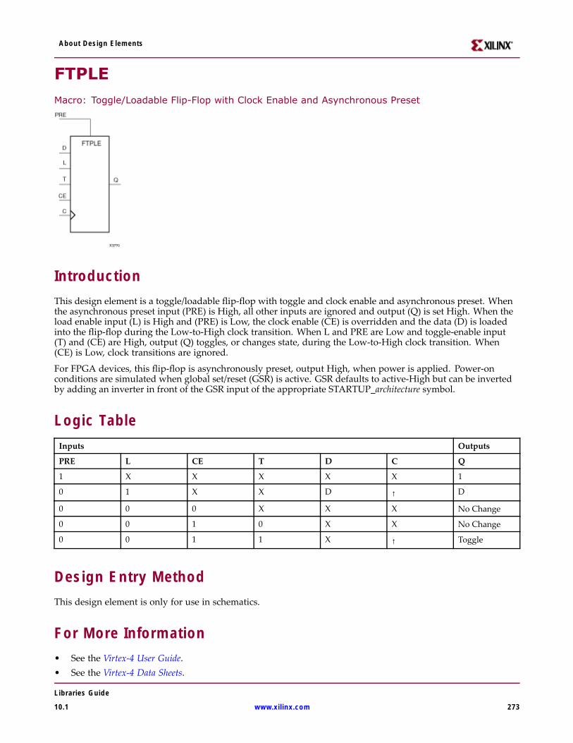
About Design Elements
FTPLEMacro: Toggle/Loadable Flip-Flop with Clock Enable and Asynchronous Preset
IntroductionThis design element is a toggle/loadable flip-flop with toggle and clock enable and asynchronous preset. Whenthe asynchronous preset input (PRE) is High, all other inputs are ignored and output (Q) is set High. When theload enable input (L) is High and (PRE) is Low, the clock enable (CE) is overridden and the data (D) is loadedinto the flip-flop during the Low-to-High clock transition. When L and PRE are Low and toggle-enable input(T) and (CE) are High, output (Q) toggles, or changes state, during the Low-to-High clock transition. When(CE) is Low, clock transitions are ignored.
For FPGA devices, this flip-flop is asynchronously preset, output High, when power is applied. Power-onconditions are simulated when global set/reset (GSR) is active. GSR defaults to active-High but can be invertedby adding an inverter in front of the GSR input of the appropriate STARTUP_architecture symbol.
Logic TableInputs Outputs
PRE L CE T D C Q
1 X X X X X 1
0 1 X X D ↑ D
0 0 0 X X X No Change
0 0 1 0 X X No Change
0 0 1 1 X ↑ Toggle
Design Entry MethodThis design element is only for use in schematics.
For More Information• See the Virtex-4 User Guide.• See the Virtex-4 Data Sheets.
Libraries Guide
10.1 www.xilinx.com 273
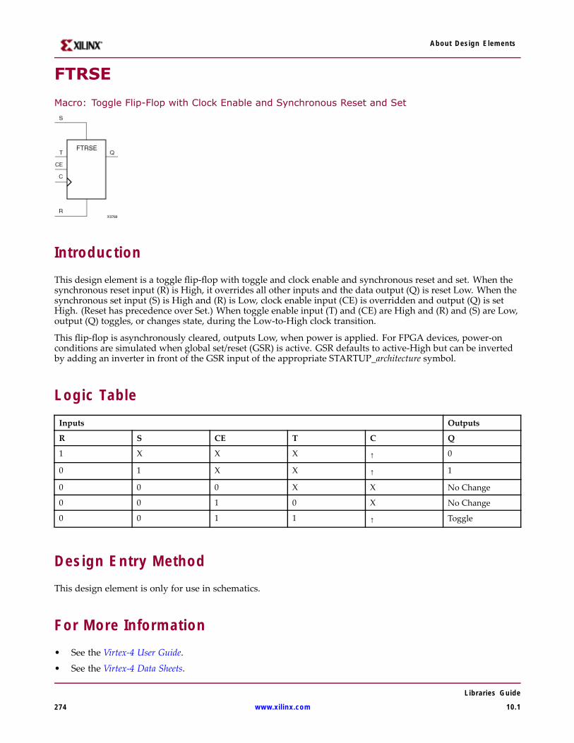
About Design Elements
FTRSE
Macro: Toggle Flip-Flop with Clock Enable and Synchronous Reset and Set
IntroductionThis design element is a toggle flip-flop with toggle and clock enable and synchronous reset and set. When thesynchronous reset input (R) is High, it overrides all other inputs and the data output (Q) is reset Low. When thesynchronous set input (S) is High and (R) is Low, clock enable input (CE) is overridden and output (Q) is setHigh. (Reset has precedence over Set.) When toggle enable input (T) and (CE) are High and (R) and (S) are Low,output (Q) toggles, or changes state, during the Low-to-High clock transition.
This flip-flop is asynchronously cleared, outputs Low, when power is applied. For FPGA devices, power-onconditions are simulated when global set/reset (GSR) is active. GSR defaults to active-High but can be invertedby adding an inverter in front of the GSR input of the appropriate STARTUP_architecture symbol.
Logic TableInputs Outputs
R S CE T C Q
1 X X X ↑ 0
0 1 X X ↑ 1
0 0 0 X X No Change
0 0 1 0 X No Change
0 0 1 1 ↑ Toggle
Design Entry MethodThis design element is only for use in schematics.
For More Information• See the Virtex-4 User Guide.
• See the Virtex-4 Data Sheets.
Libraries Guide
274 www.xilinx.com 10.1
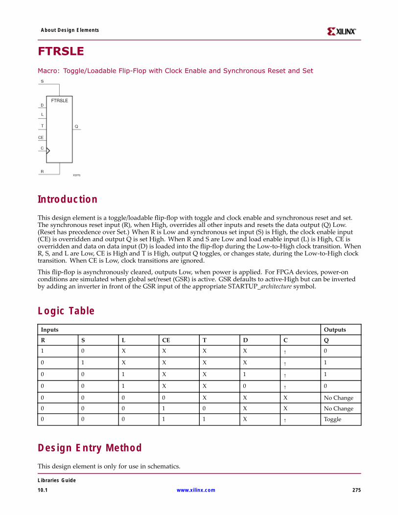
About Design Elements
FTRSLE
Macro: Toggle/Loadable Flip-Flop with Clock Enable and Synchronous Reset and Set
IntroductionThis design element is a toggle/loadable flip-flop with toggle and clock enable and synchronous reset and set.The synchronous reset input (R), when High, overrides all other inputs and resets the data output (Q) Low.(Reset has precedence over Set.) When R is Low and synchronous set input (S) is High, the clock enable input(CE) is overridden and output Q is set High. When R and S are Low and load enable input (L) is High, CE isoverridden and data on data input (D) is loaded into the flip-flop during the Low-to-High clock transition. WhenR, S, and L are Low, CE is High and T is High, output Q toggles, or changes state, during the Low-to-High clocktransition. When CE is Low, clock transitions are ignored.
This flip-flop is asynchronously cleared, outputs Low, when power is applied. For FPGA devices, power-onconditions are simulated when global set/reset (GSR) is active. GSR defaults to active-High but can be invertedby adding an inverter in front of the GSR input of the appropriate STARTUP_architecture symbol.
Logic TableInputs Outputs
R S L CE T D C Q
1 0 X X X X ↑ 0
0 1 X X X X ↑ 1
0 0 1 X X 1 ↑ 1
0 0 1 X X 0 ↑ 0
0 0 0 0 X X X No Change
0 0 0 1 0 X X No Change
0 0 0 1 1 X ↑ Toggle
Design Entry MethodThis design element is only for use in schematics.
Libraries Guide
10.1 www.xilinx.com 275

About Design Elements
For More Information• See the Virtex-4 User Guide.
• See the Virtex-4 Data Sheets.
Libraries Guide
276 www.xilinx.com 10.1
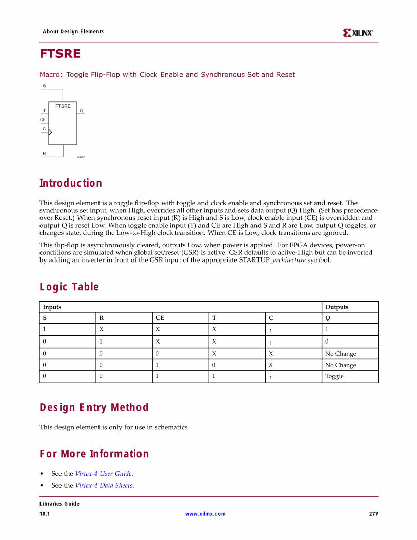
About Design Elements
FTSRE
Macro: Toggle Flip-Flop with Clock Enable and Synchronous Set and Reset
IntroductionThis design element is a toggle flip-flop with toggle and clock enable and synchronous set and reset. Thesynchronous set input, when High, overrides all other inputs and sets data output (Q) High. (Set has precedenceover Reset.) When synchronous reset input (R) is High and S is Low, clock enable input (CE) is overridden andoutput Q is reset Low. When toggle enable input (T) and CE are High and S and R are Low, output Q toggles, orchanges state, during the Low-to-High clock transition. When CE is Low, clock transitions are ignored.
This flip-flop is asynchronously cleared, outputs Low, when power is applied. For FPGA devices, power-onconditions are simulated when global set/reset (GSR) is active. GSR defaults to active-High but can be invertedby adding an inverter in front of the GSR input of the appropriate STARTUP_architecture symbol.
Logic TableInputs Outputs
S R CE T C Q
1 X X X ↑ 1
0 1 X X ↑ 0
0 0 0 X X No Change
0 0 1 0 X No Change
0 0 1 1 ↑ Toggle
Design Entry MethodThis design element is only for use in schematics.
For More Information• See the Virtex-4 User Guide.
• See the Virtex-4 Data Sheets.
Libraries Guide
10.1 www.xilinx.com 277
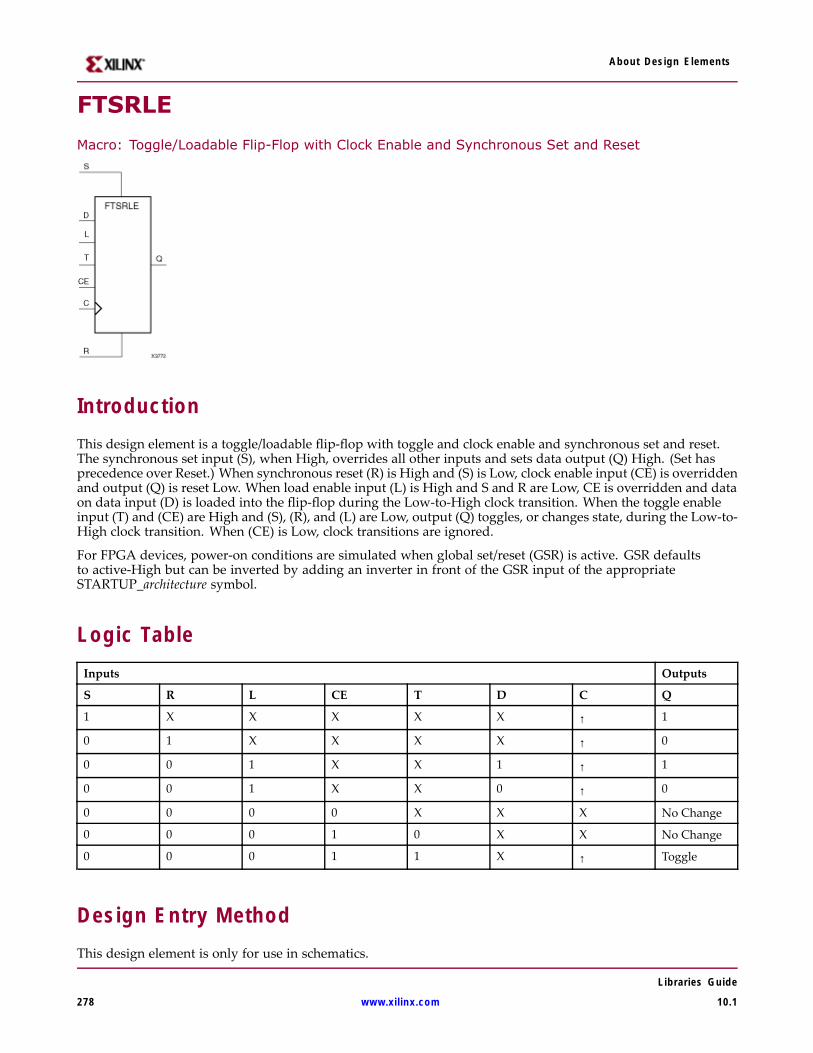
About Design Elements
FTSRLE
Macro: Toggle/Loadable Flip-Flop with Clock Enable and Synchronous Set and Reset
IntroductionThis design element is a toggle/loadable flip-flop with toggle and clock enable and synchronous set and reset.The synchronous set input (S), when High, overrides all other inputs and sets data output (Q) High. (Set hasprecedence over Reset.) When synchronous reset (R) is High and (S) is Low, clock enable input (CE) is overriddenand output (Q) is reset Low. When load enable input (L) is High and S and R are Low, CE is overridden and dataon data input (D) is loaded into the flip-flop during the Low-to-High clock transition. When the toggle enableinput (T) and (CE) are High and (S), (R), and (L) are Low, output (Q) toggles, or changes state, during the Low-to-High clock transition. When (CE) is Low, clock transitions are ignored.
For FPGA devices, power-on conditions are simulated when global set/reset (GSR) is active. GSR defaultsto active-High but can be inverted by adding an inverter in front of the GSR input of the appropriateSTARTUP_architecture symbol.
Logic TableInputs Outputs
S R L CE T D C Q
1 X X X X X ↑ 1
0 1 X X X X ↑ 0
0 0 1 X X 1 ↑ 1
0 0 1 X X 0 ↑ 0
0 0 0 0 X X X No Change
0 0 0 1 0 X X No Change
0 0 0 1 1 X ↑ Toggle
Design Entry MethodThis design element is only for use in schematics.
Libraries Guide
278 www.xilinx.com 10.1

About Design Elements
For More Information• See the Virtex-4 User Guide.
• See the Virtex-4 Data Sheets.
Libraries Guide
10.1 www.xilinx.com 279
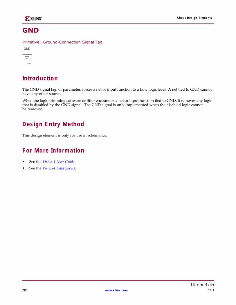
About Design Elements
GND
Primitive: Ground-Connection Signal Tag
IntroductionThe GND signal tag, or parameter, forces a net or input function to a Low logic level. A net tied to GND cannothave any other source.
When the logic-trimming software or fitter encounters a net or input function tied to GND, it removes any logicthat is disabled by the GND signal. The GND signal is only implemented when the disabled logic cannotbe removed.
Design Entry MethodThis design element is only for use in schematics.
For More Information• See the Virtex-4 User Guide.
• See the Virtex-4 Data Sheets.
Libraries Guide
280 www.xilinx.com 10.1
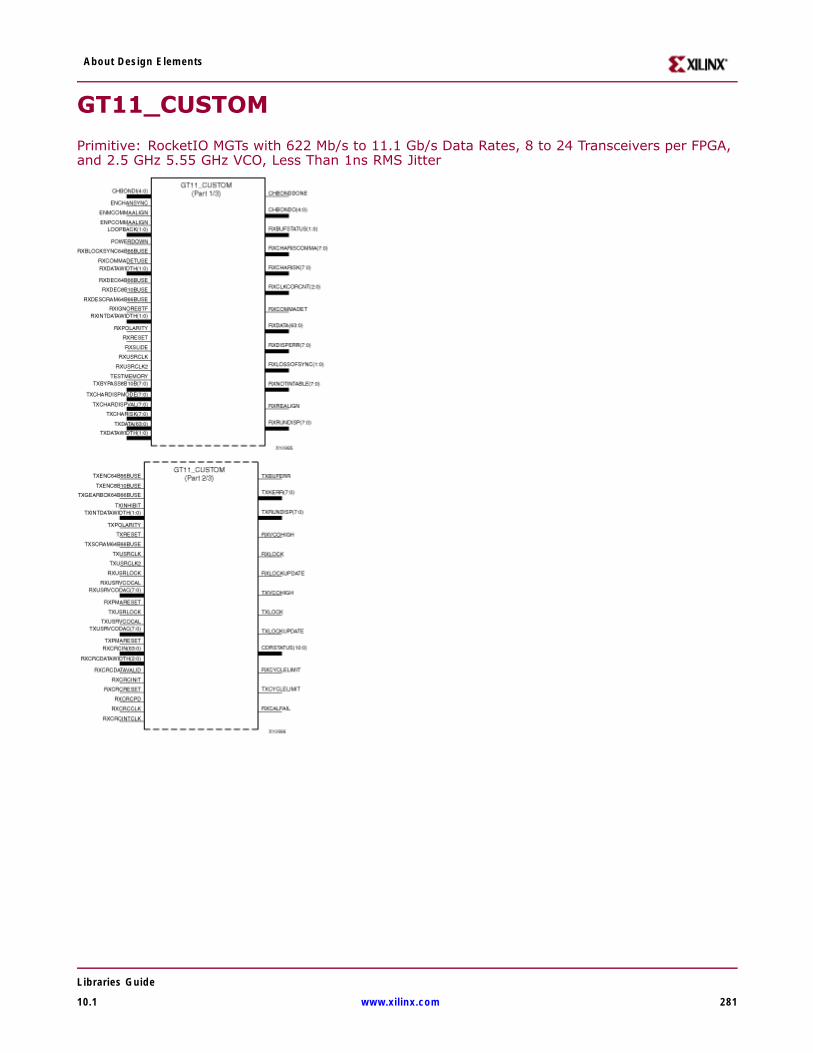
About Design Elements
GT11_CUSTOM
Primitive: RocketIO MGTs with 622 Mb/s to 11.1 Gb/s Data Rates, 8 to 24 Transceivers per FPGA,and 2.5 GHz 5.55 GHz VCO, Less Than 1ns RMS Jitter
Libraries Guide
10.1 www.xilinx.com 281
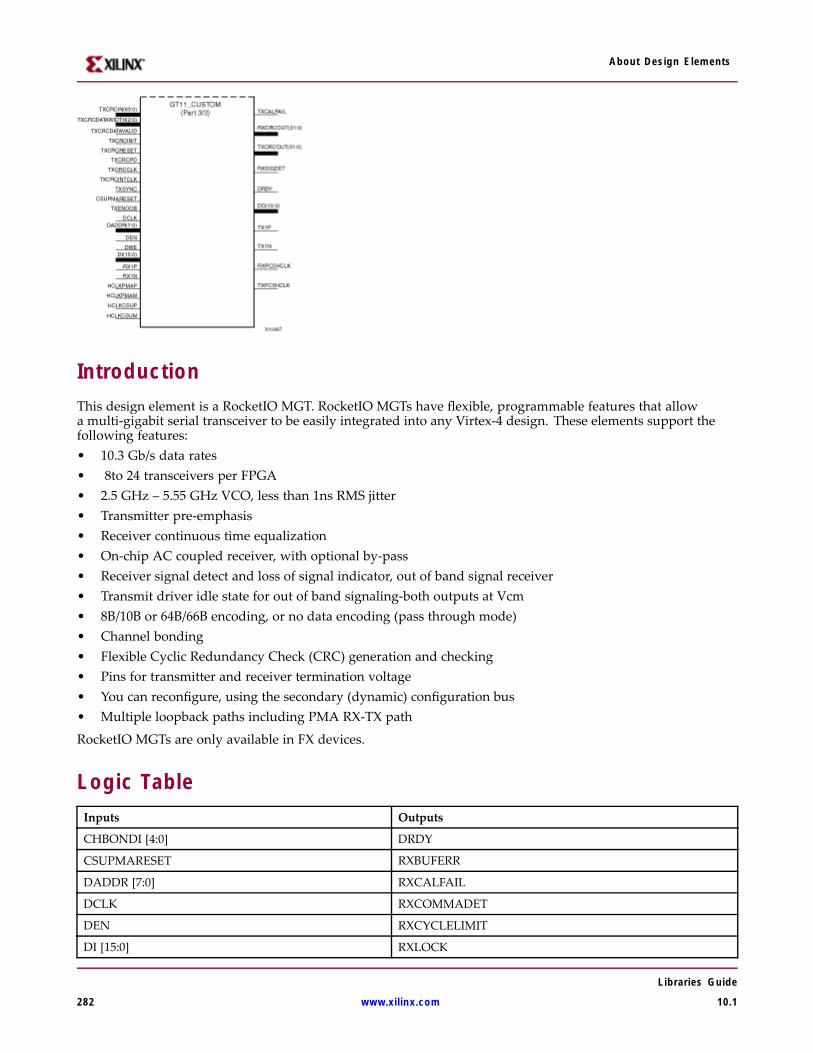
About Design Elements
IntroductionThis design element is a RocketIO MGT. RocketIO MGTs have flexible, programmable features that allowa multi-gigabit serial transceiver to be easily integrated into any Virtex-4 design. These elements support thefollowing features:• 10.3 Gb/s data rates• 8to 24 transceivers per FPGA• 2.5 GHz – 5.55 GHz VCO, less than 1ns RMS jitter• Transmitter pre-emphasis• Receiver continuous time equalization• On-chip AC coupled receiver, with optional by-pass• Receiver signal detect and loss of signal indicator, out of band signal receiver• Transmit driver idle state for out of band signaling-both outputs at Vcm• 8B/10B or 64B/66B encoding, or no data encoding (pass through mode)• Channel bonding• Flexible Cyclic Redundancy Check (CRC) generation and checking• Pins for transmitter and receiver termination voltage• You can reconfigure, using the secondary (dynamic) configuration bus• Multiple loopback paths including PMA RX-TX path
RocketIO MGTs are only available in FX devices.
Logic TableInputs Outputs
CHBONDI [4:0] DRDY
CSUPMARESET RXBUFERR
DADDR [7:0] RXCALFAIL
DCLK RXCOMMADET
DEN RXCYCLELIMIT
DI [15:0] RXLOCK
Libraries Guide
282 www.xilinx.com 10.1
About Design Elements
Inputs Outputs
DWE RXRealIGN
ENCHANSYNC RXRECCLK1
ENMCOMMAALIGN RXBCLK
ENPCOMMAALIGN RXRECCLK2
GREFCLK RXSIGDET
LOOPBACK [1:0] TX1N
POWERDOWN TX1P
REFCLK1 TXBUFERR
REFCLK2 TXCALFAIL
RX1N TXCYCLELIMIT
RX1P TXLOCK
RXBLOCKSYNC64B66BUSE DO [15:0]
RXCLKSTABLE RXLOSSOFSYNC [1:0]
RXCOMMADETUSE RXCRCOUT [31:0]
RXCRCCLK TXCRCOUT [31:0]
RXCRCDATAVALID CHBONDO [4:0]
RXCRCDATAWIDTH [2:0] RXSTATUS [5:0]
RXCRCIN [63:0] RXDATA [63:0]
RXCRCINIT RXCHARISCOMMA [7:0]
RXCRCINTCLK RXCHARISK [7:0]
RXCRCPD RXDISPERR [7:0]
RXCRCRESET RXNOTINTABLE [7:0]
RXDATAWIDTH [1:0] RXRUNDISP [7:0]
RXDEC64B66BUSE TXRUNDISP [7:0]
RXDEC8B10BUSE TXKERR [7:0]
RXDESCRAM64B66BUSE
RXIGNOREBTF
RXINTDATAWIDTH [1:0]
RXPMARESET
RXPOLARITY
RXRESET
RXSLIDE
RXUSRCLK
RXUSRCLK2
TXBYPASS8B10B [7:0]
TXCHARDISPMODE [7:0]
TXCHARDISPVAL [7:0]
TXCHARISK [7:0]
Libraries Guide
10.1 www.xilinx.com 283
About Design Elements
Inputs Outputs
TXCLKSTABLE
TXCRCCLK
TXCRCDATAVALID
TXCRCDATAWIDTH [2:0]
TXCRCIN [63:0]
TXCRCINIT
TXCRCINTCLK
TXCRCPD
TXCRCRESET
TXDATA [63:0]
TXDATAWIDTH [1:0]
TXENC64B66BUSE
TXENC8B10BUSE
TXENOOB
TXGEARBOX64B66BUSE
TXINHIBIT
TXINTDATAWIDTH [1:0]
TXPMARESET
TXPOLARITY
TXRESET
TXSCRAM64B66BUSE
TXSYNC
TXUSRCLK
TXUSRCLK2
Design Entry MethodThis design element can be used in schematics.
For More Information• See the Virtex-4 User Guide.
• See the Virtex-4 Data Sheets.
Libraries Guide
284 www.xilinx.com 10.1
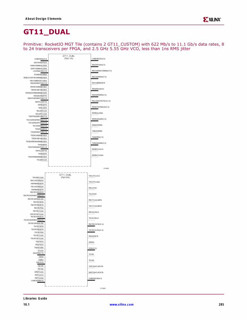
About Design Elements
GT11_DUAL
Primitive: RocketIO MGT Tile (contains 2 GT11_CUSTOM) with 622 Mb/s to 11.1 Gb/s data rates, 8to 24 transceivers per FPGA, and 2.5 GHz 5.55 GHz VCO, less than 1ns RMS jitter
Libraries Guide
10.1 www.xilinx.com 285
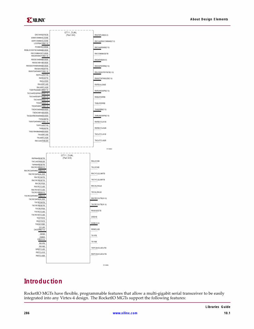
About Design Elements
IntroductionRocketIO MGTs have flexible, programmable features that allow a multi-gigabit serial transceiver to be easilyintegrated into any Virtex-4 design. The RocketIO MGTs support the following features:
Libraries Guide
286 www.xilinx.com 10.1
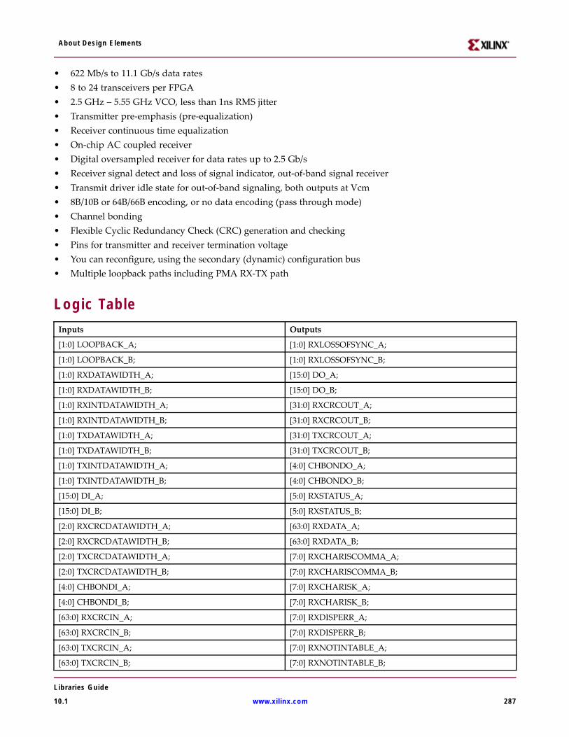
About Design Elements
• 622 Mb/s to 11.1 Gb/s data rates• 8 to 24 transceivers per FPGA• 2.5 GHz – 5.55 GHz VCO, less than 1ns RMS jitter• Transmitter pre-emphasis (pre-equalization)• Receiver continuous time equalization• On-chip AC coupled receiver• Digital oversampled receiver for data rates up to 2.5 Gb/s• Receiver signal detect and loss of signal indicator, out-of-band signal receiver• Transmit driver idle state for out-of-band signaling, both outputs at Vcm• 8B/10B or 64B/66B encoding, or no data encoding (pass through mode)• Channel bonding• Flexible Cyclic Redundancy Check (CRC) generation and checking• Pins for transmitter and receiver termination voltage• You can reconfigure, using the secondary (dynamic) configuration bus• Multiple loopback paths including PMA RX-TX path
Logic TableInputs Outputs
[1:0] LOOPBACK_A; [1:0] RXLOSSOFSYNC_A;
[1:0] LOOPBACK_B; [1:0] RXLOSSOFSYNC_B;
[1:0] RXDATAWIDTH_A; [15:0] DO_A;
[1:0] RXDATAWIDTH_B; [15:0] DO_B;
[1:0] RXINTDATAWIDTH_A; [31:0] RXCRCOUT_A;
[1:0] RXINTDATAWIDTH_B; [31:0] RXCRCOUT_B;
[1:0] TXDATAWIDTH_A; [31:0] TXCRCOUT_A;
[1:0] TXDATAWIDTH_B; [31:0] TXCRCOUT_B;
[1:0] TXINTDATAWIDTH_A; [4:0] CHBONDO_A;
[1:0] TXINTDATAWIDTH_B; [4:0] CHBONDO_B;
[15:0] DI_A; [5:0] RXSTATUS_A;
[15:0] DI_B; [5:0] RXSTATUS_B;
[2:0] RXCRCDATAWIDTH_A; [63:0] RXDATA_A;
[2:0] RXCRCDATAWIDTH_B; [63:0] RXDATA_B;
[2:0] TXCRCDATAWIDTH_A; [7:0] RXCHARISCOMMA_A;
[2:0] TXCRCDATAWIDTH_B; [7:0] RXCHARISCOMMA_B;
[4:0] CHBONDI_A; [7:0] RXCHARISK_A;
[4:0] CHBONDI_B; [7:0] RXCHARISK_B;
[63:0] RXCRCIN_A; [7:0] RXDISPERR_A;
[63:0] RXCRCIN_B; [7:0] RXDISPERR_B;
[63:0] TXCRCIN_A; [7:0] RXNOTINTABLE_A;
[63:0] TXCRCIN_B; [7:0] RXNOTINTABLE_B;
Libraries Guide
10.1 www.xilinx.com 287
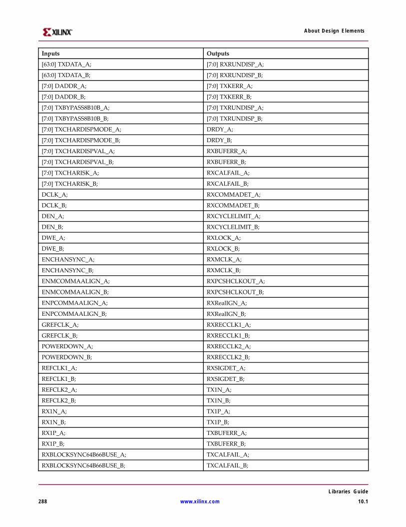
About Design Elements
Inputs Outputs
[63:0] TXDATA_A; [7:0] RXRUNDISP_A;
[63:0] TXDATA_B; [7:0] RXRUNDISP_B;
[7:0] DADDR_A; [7:0] TXKERR_A;
[7:0] DADDR_B; [7:0] TXKERR_B;
[7:0] TXBYPASS8B10B_A; [7:0] TXRUNDISP_A;
[7:0] TXBYPASS8B10B_B; [7:0] TXRUNDISP_B;
[7:0] TXCHARDISPMODE_A; DRDY_A;
[7:0] TXCHARDISPMODE_B; DRDY_B;
[7:0] TXCHARDISPVAL_A; RXBUFERR_A;
[7:0] TXCHARDISPVAL_B; RXBUFERR_B;
[7:0] TXCHARISK_A; RXCALFAIL_A;
[7:0] TXCHARISK_B; RXCALFAIL_B;
DCLK_A; RXCOMMADET_A;
DCLK_B; RXCOMMADET_B;
DEN_A; RXCYCLELIMIT_A;
DEN_B; RXCYCLELIMIT_B;
DWE_A; RXLOCK_A;
DWE_B; RXLOCK_B;
ENCHANSYNC_A; RXMCLK_A;
ENCHANSYNC_B; RXMCLK_B;
ENMCOMMAALIGN_A; RXPCSHCLKOUT_A;
ENMCOMMAALIGN_B; RXPCSHCLKOUT_B;
ENPCOMMAALIGN_A; RXRealIGN_A;
ENPCOMMAALIGN_B; RXRealIGN_B;
GREFCLK_A; RXRECCLK1_A;
GREFCLK_B; RXRECCLK1_B;
POWERDOWN_A; RXRECCLK2_A;
POWERDOWN_B; RXRECCLK2_B;
REFCLK1_A; RXSIGDET_A;
REFCLK1_B; RXSIGDET_B;
REFCLK2_A; TX1N_A;
REFCLK2_B; TX1N_B;
RX1N_A; TX1P_A;
RX1N_B; TX1P_B;
RX1P_A; TXBUFERR_A;
RX1P_B; TXBUFERR_B;
RXBLOCKSYNC64B66BUSE_A; TXCALFAIL_A;
RXBLOCKSYNC64B66BUSE_B; TXCALFAIL_B;
Libraries Guide
288 www.xilinx.com 10.1
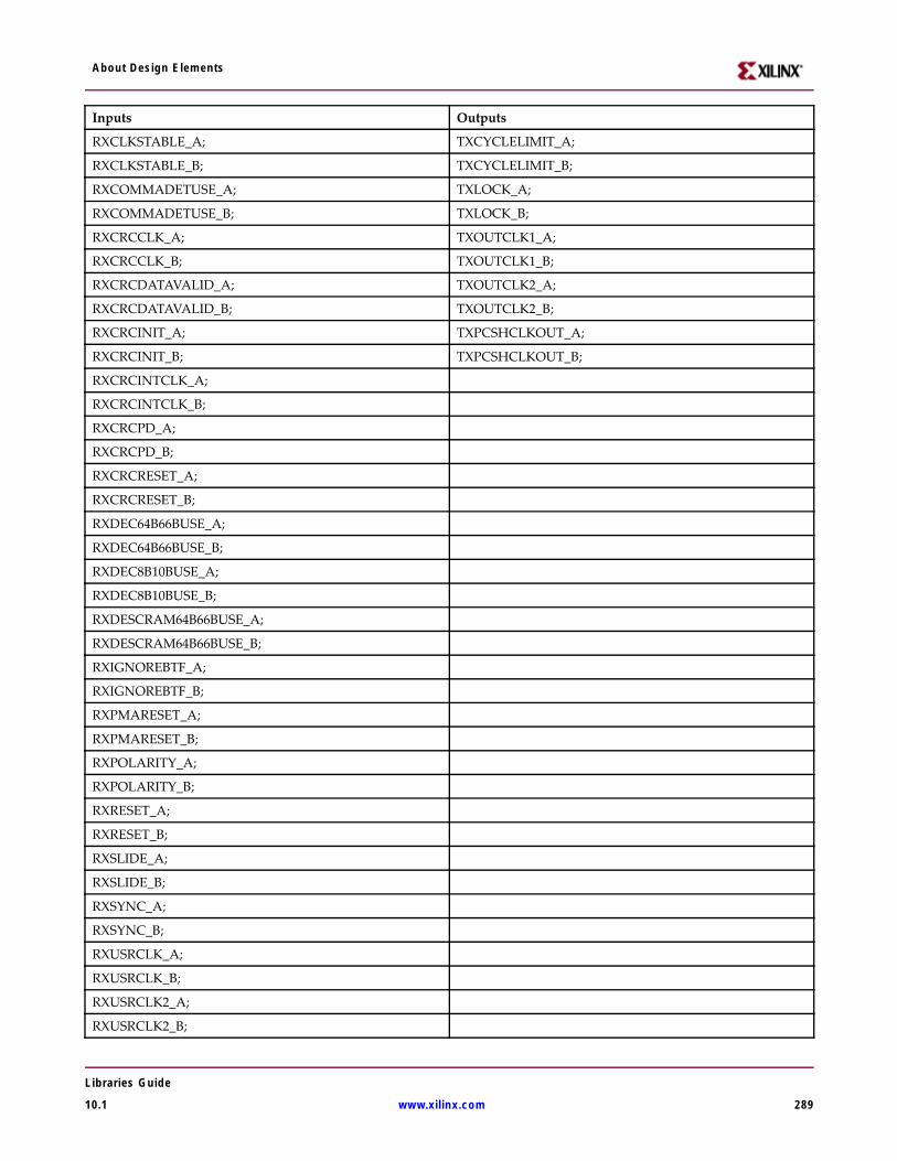
About Design Elements
Inputs Outputs
RXCLKSTABLE_A; TXCYCLELIMIT_A;
RXCLKSTABLE_B; TXCYCLELIMIT_B;
RXCOMMADETUSE_A; TXLOCK_A;
RXCOMMADETUSE_B; TXLOCK_B;
RXCRCCLK_A; TXOUTCLK1_A;
RXCRCCLK_B; TXOUTCLK1_B;
RXCRCDATAVALID_A; TXOUTCLK2_A;
RXCRCDATAVALID_B; TXOUTCLK2_B;
RXCRCINIT_A; TXPCSHCLKOUT_A;
RXCRCINIT_B; TXPCSHCLKOUT_B;
RXCRCINTCLK_A;
RXCRCINTCLK_B;
RXCRCPD_A;
RXCRCPD_B;
RXCRCRESET_A;
RXCRCRESET_B;
RXDEC64B66BUSE_A;
RXDEC64B66BUSE_B;
RXDEC8B10BUSE_A;
RXDEC8B10BUSE_B;
RXDESCRAM64B66BUSE_A;
RXDESCRAM64B66BUSE_B;
RXIGNOREBTF_A;
RXIGNOREBTF_B;
RXPMARESET_A;
RXPMARESET_B;
RXPOLARITY_A;
RXPOLARITY_B;
RXRESET_A;
RXRESET_B;
RXSLIDE_A;
RXSLIDE_B;
RXSYNC_A;
RXSYNC_B;
RXUSRCLK_A;
RXUSRCLK_B;
RXUSRCLK2_A;
RXUSRCLK2_B;
Libraries Guide
10.1 www.xilinx.com 289
About Design Elements
Inputs Outputs
TXCLKSTABLE_A;
TXCLKSTABLE_B;
TXCRCCLK_A;
TXCRCCLK_B;
TXCRCDATAVALID_A;
TXCRCDATAVALID_B;
TXCRCINIT_A;
TXCRCINIT_B;
TXCRCINTCLK_A;
TXCRCINTCLK_B;
TXCRCPD_A;
TXCRCPD_B;
TXCRCRESET_A;
TXCRCRESET_B;
TXENC64B66BUSE_A;
TXENC64B66BUSE_B;
TXENC8B10BUSE_A;
TXENC8B10BUSE_B;
TXENOOB_A;
TXENOOB_B;
TXGEARBOX64B66BUSE_A;
TXGEARBOX64B66BUSE_B;
TXINHIBIT_A;
TXINHIBIT_B;
TXPMARESET_A;
TXPMARESET_B;
TXPOLARITY_A;
TXPOLARITY_B;
TXRESET_A;
TXRESET_B;
TXSCRAM64B66BUSE_A;
TXSCRAM64B66BUSE_B;
TXSYNC_A;
TXSYNC_B;
TXUSRCLK_A;
TXUSRCLK_B;
TXUSRCLK2_A;
TXUSRCLK2_B;
Libraries Guide
290 www.xilinx.com 10.1

About Design Elements
Design Entry MethodThis design element can be used in schematics.
For More Information• See the Virtex-4 User Guide.
• See the Virtex-4 Data Sheets.
Libraries Guide
10.1 www.xilinx.com 291
About Design Elements
GT11CLK
Primitive: A MUX That Can Select Fom Differential Package Input Clock, refclk From the Fabric, orrxbclk to Drive the Two Vertical Reference Clock Buses for the Column of MGTs
IntroductionThis block needs to be instantiated when using the dedicated package pins for RocketIO clocks. There are twoavailable per MGT column.The attributes allow this package input to drive one or both SYNCLK clock trees.Please see the Virtex-4 RocketIO MGT User Guide for more details.
The attribute REFCLKSEL allows more clocking options. These options include: MGTCLK, SYNCLK1IN,SYNCLK2IN, REFCLK, RXBCLK.
Port Descriptions
Inputs are MGTCLKP, MGTCLKN
Outputs are SYNCLK1OUT, SYNCLK2OUT
Design Entry MethodThis design element can be used in schematics.
For More Information• See the Virtex-4 User Guide.
• See the Virtex-4 Data Sheets.
Libraries Guide
292 www.xilinx.com 10.1
About Design Elements
GT11CLK_MGT
Primitive: Allows Differential Package Input to Drive the Two Vertical Reference Clock Buses forthe Column of MGTs
IntroductionThis block needs to be instantiated when using the dedicated package pins for RocketIO clocks. There are twoavailable per MGT column.The attributes allow this package input to drive one or both SYNCLK clock trees.Please see the Virtex-4 RocketIO MGT User Guide for more details.
Port DescriptionInputs are MGTCLKP, MGTCLKN
Outputs are SYNCLK1OUT, SYNCLK2OUT
Design Entry MethodThis design element can be used in schematics.
For More Information• See the Virtex-4 User Guide.
• See the Virtex-4 Data Sheets.
Libraries Guide
10.1 www.xilinx.com 293

About Design Elements
IBUF
Primitive: Input Buffer
IntroductionThis design element is automatically inserted (inferred) by the synthesis tool to any signal directly connectedto a top-level input or in-out port of the design. You should generally let the synthesis tool infer this buffer.However, it can be instantiated into the design if required. In order to do so, connect the input port (I) directly tothe associated top-level input or in-out port, and connect the output port (O) to the logic sourced by that port.Modify any necessary generic maps (VHDL) or named parameter value assignment (Verilog) in order to changethe default behavior of the component.
Port DescriptionsPort Direction Width Function
O Output 1 Buffer input
I Input 1 Buffer output
Design Entry MethodThis design element can be used in schematics.
In general, this element is inferred by the synthesis tool for any specified top-level input port to the design. It isgenerally not necessary to specify them in the source code however if desired, they be manually instantiated byeither copying the instantiation code from the ISE Libraries Guide HDL Template and paste it into the top-levelentity/module of your code. It is recommended to always put all I/O components on the top-level of the design tohelp facilitate hierarchical design methods. Connect the I port directly to the top-level input port of the designand the O port to the logic in which this input is to source. Specify the desired generic/defparam values inorder to configure the proper behavior of the buffer.
Available AttributesAttribute Type Allowed Values Default Description
CAPACITANCE String "LOW", "NORMAL","DONT_CARE"
"DONT_ CARE" Specified whether the I/O should beused with lower or normal intrinsiccapacitance.
IOSTANDARD String See Data Sheet "DEFAULT" Assigns an I/O standard to theelement.
Libraries Guide
294 www.xilinx.com 10.1

About Design Elements
For More Information• See the Virtex-4 User Guide.
• See the Virtex-4 Data Sheets.
Libraries Guide
10.1 www.xilinx.com 295
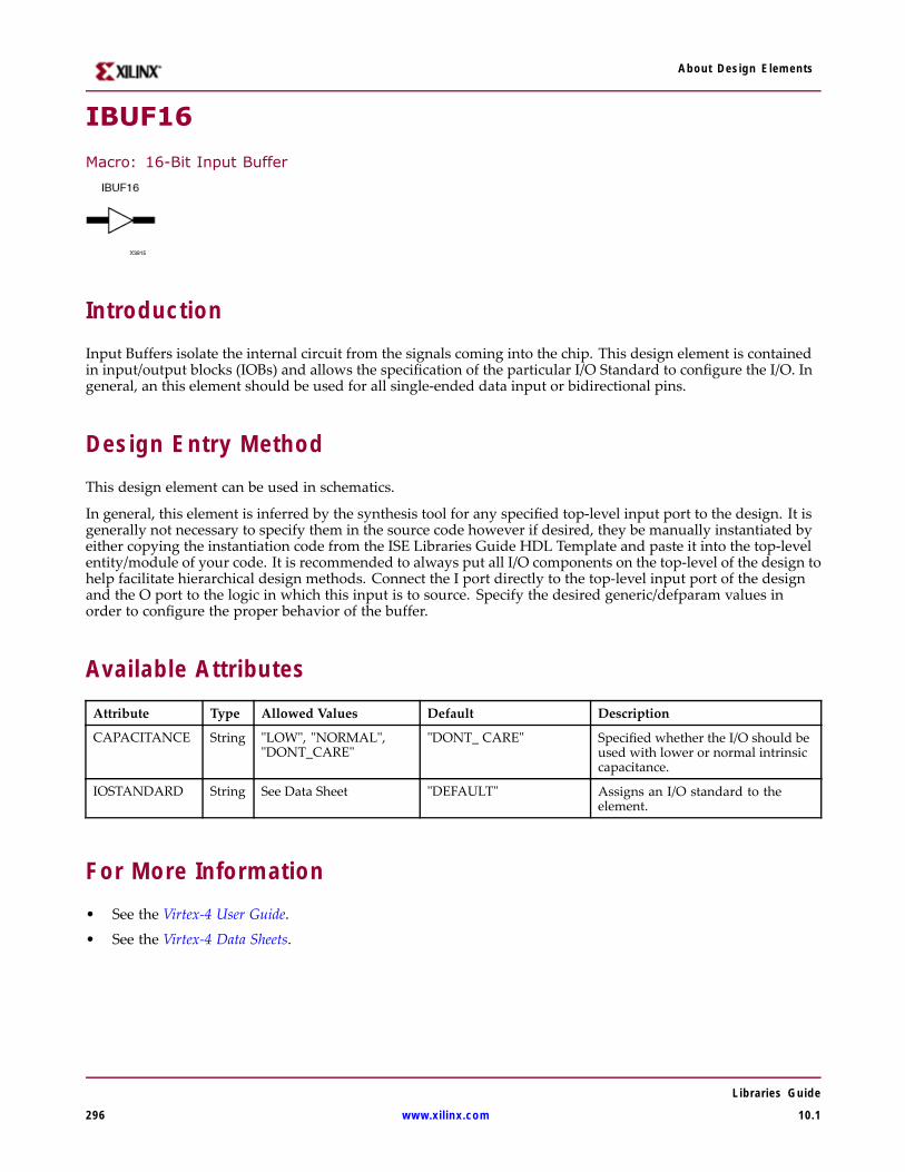
About Design Elements
IBUF16
Macro: 16-Bit Input Buffer
IntroductionInput Buffers isolate the internal circuit from the signals coming into the chip. This design element is containedin input/output blocks (IOBs) and allows the specification of the particular I/O Standard to configure the I/O. Ingeneral, an this element should be used for all single-ended data input or bidirectional pins.
Design Entry MethodThis design element can be used in schematics.
In general, this element is inferred by the synthesis tool for any specified top-level input port to the design. It isgenerally not necessary to specify them in the source code however if desired, they be manually instantiated byeither copying the instantiation code from the ISE Libraries Guide HDL Template and paste it into the top-levelentity/module of your code. It is recommended to always put all I/O components on the top-level of the design tohelp facilitate hierarchical design methods. Connect the I port directly to the top-level input port of the designand the O port to the logic in which this input is to source. Specify the desired generic/defparam values inorder to configure the proper behavior of the buffer.
Available AttributesAttribute Type Allowed Values Default Description
CAPACITANCE String "LOW", "NORMAL","DONT_CARE"
"DONT_ CARE" Specified whether the I/O should beused with lower or normal intrinsiccapacitance.
IOSTANDARD String See Data Sheet "DEFAULT" Assigns an I/O standard to theelement.
For More Information• See the Virtex-4 User Guide.
• See the Virtex-4 Data Sheets.
Libraries Guide
296 www.xilinx.com 10.1

About Design Elements
IBUF4
Macro: 4-Bit Input Buffer
IntroductionInput Buffers isolate the internal circuit from the signals coming into the chip. This design element is containedin input/output blocks (IOBs) and allows the specification of the particular I/O Standard to configure the I/O. Ingeneral, an this element should be used for all single-ended data input or bidirectional pins.
Design Entry MethodThis design element can be used in schematics.
In general, this element is inferred by the synthesis tool for any specified top-level input port to the design. It isgenerally not necessary to specify them in the source code however if desired, they be manually instantiated byeither copying the instantiation code from the ISE Libraries Guide HDL Template and paste it into the top-levelentity/module of your code. It is recommended to always put all I/O components on the top-level of the design tohelp facilitate hierarchical design methods. Connect the I port directly to the top-level input port of the designand the O port to the logic in which this input is to source. Specify the desired generic/defparam values inorder to configure the proper behavior of the buffer.
Available AttributesAttribute Type Allowed Values Default Description
CAPACITANCE String "LOW", "NORMAL","DONT_CARE"
"DONT_ CARE" Specified whether the I/O should beused with lower or normal intrinsiccapacitance.
IOSTANDARD String See Data Sheet "DEFAULT" Assigns an I/O standard to theelement.
For More Information• See the Virtex-4 User Guide.
• See the Virtex-4 Data Sheets.
Libraries Guide
10.1 www.xilinx.com 297
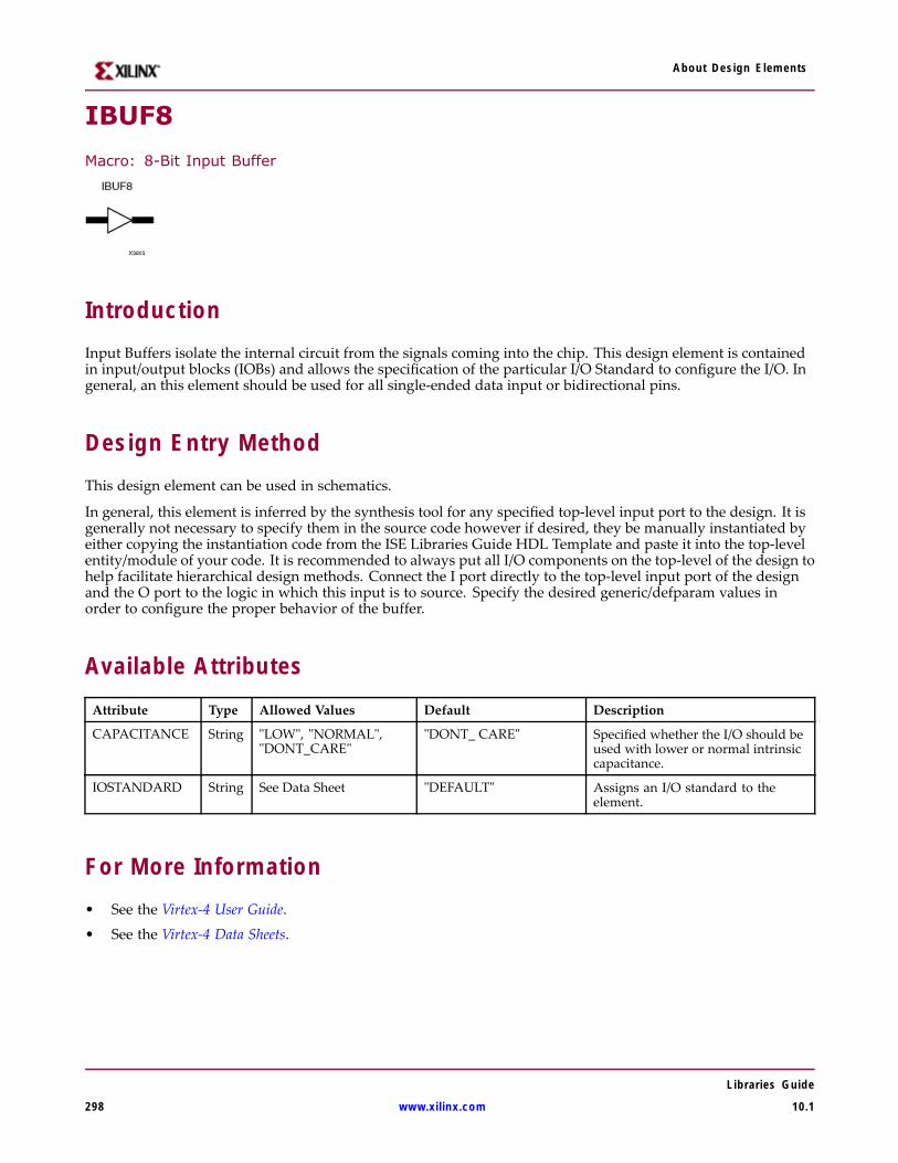
About Design Elements
IBUF8
Macro: 8-Bit Input Buffer
IntroductionInput Buffers isolate the internal circuit from the signals coming into the chip. This design element is containedin input/output blocks (IOBs) and allows the specification of the particular I/O Standard to configure the I/O. Ingeneral, an this element should be used for all single-ended data input or bidirectional pins.
Design Entry MethodThis design element can be used in schematics.
In general, this element is inferred by the synthesis tool for any specified top-level input port to the design. It isgenerally not necessary to specify them in the source code however if desired, they be manually instantiated byeither copying the instantiation code from the ISE Libraries Guide HDL Template and paste it into the top-levelentity/module of your code. It is recommended to always put all I/O components on the top-level of the design tohelp facilitate hierarchical design methods. Connect the I port directly to the top-level input port of the designand the O port to the logic in which this input is to source. Specify the desired generic/defparam values inorder to configure the proper behavior of the buffer.
Available AttributesAttribute Type Allowed Values Default Description
CAPACITANCE String "LOW", "NORMAL","DONT_CARE"
"DONT_ CARE" Specified whether the I/O should beused with lower or normal intrinsiccapacitance.
IOSTANDARD String See Data Sheet "DEFAULT" Assigns an I/O standard to theelement.
For More Information• See the Virtex-4 User Guide.
• See the Virtex-4 Data Sheets.
Libraries Guide
298 www.xilinx.com 10.1
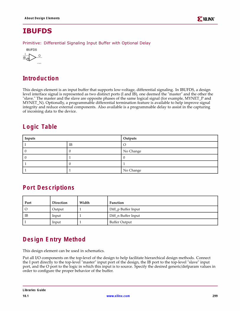
About Design Elements
IBUFDS
Primitive: Differential Signaling Input Buffer with Optional Delay
IntroductionThis design element is an input buffer that supports low-voltage, differential signaling. In IBUFDS, a designlevel interface signal is represented as two distinct ports (I and IB), one deemed the "master" and the other the"slave." The master and the slave are opposite phases of the same logical signal (for example, MYNET_P andMYNET_N). Optionally, a programmable differential termination feature is available to help improve signalintegrity and reduce external components. Also available is a programmable delay to assist in the capturingof incoming data to the device.
Logic TableInputs Outputs
I IB O
0 0 No Change
0 1 0
1 0 1
1 1 No Change
Port Descriptions
Port Direction Width Function
O Output 1 Diff_p Buffer Input
IB Input 1 Diff_n Buffer Input
I Input 1 Buffer Output
Design Entry MethodThis design element can be used in schematics.
Put all I/O components on the top-level of the design to help facilitate hierarchical design methods. Connectthe I port directly to the top-level "master" input port of the design, the IB port to the top-level "slave" inputport, and the O port to the logic in which this input is to source. Specify the desired generic/defparam values inorder to configure the proper behavior of the buffer.
Libraries Guide
10.1 www.xilinx.com 299
About Design Elements
Available Attributes
Attribute TypeAllowedValues Default Description
CAPACITANCE String "LOW","NORMAL","DONT_CARE"
"DONT_CARE"
Specified whether the I/O should be used with lower ornormal intrinsic capacitance.
DIFF_TERM Boolean TRUE orFALSE
FALSE Enables the built-in differential termination resistor.
IOSTANDARD String See Data Sheet "DEFAULT" Assigns an I/O standard to the element.
For More Information• See the Virtex-4 User Guide.
• See the Virtex-4 Data Sheets.
Libraries Guide
300 www.xilinx.com 10.1
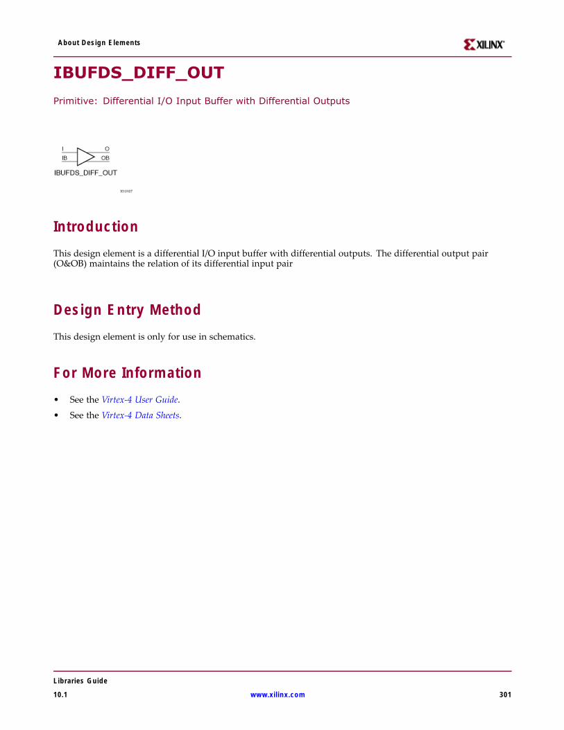
About Design Elements
IBUFDS_DIFF_OUT
Primitive: Differential I/O Input Buffer with Differential Outputs
IntroductionThis design element is a differential I/O input buffer with differential outputs. The differential output pair(O&OB) maintains the relation of its differential input pair
Design Entry MethodThis design element is only for use in schematics.
For More Information• See the Virtex-4 User Guide.
• See the Virtex-4 Data Sheets.
Libraries Guide
10.1 www.xilinx.com 301
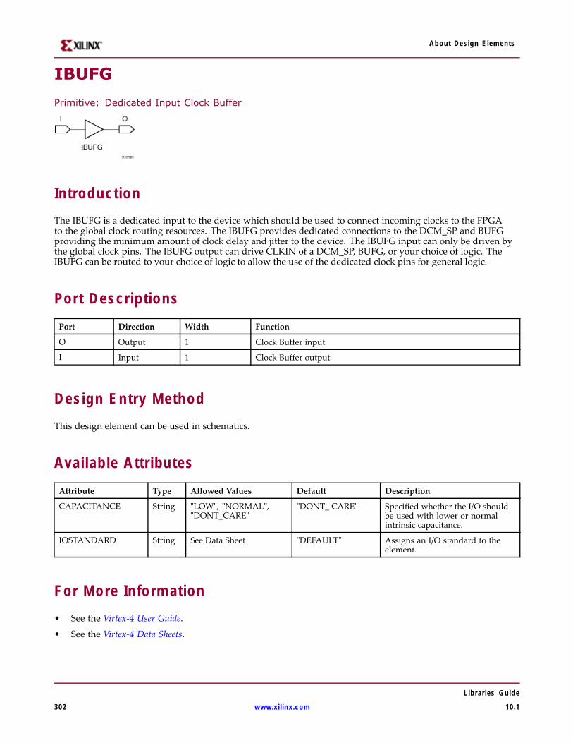
About Design Elements
IBUFG
Primitive: Dedicated Input Clock Buffer
IntroductionThe IBUFG is a dedicated input to the device which should be used to connect incoming clocks to the FPGAto the global clock routing resources. The IBUFG provides dedicated connections to the DCM_SP and BUFGproviding the minimum amount of clock delay and jitter to the device. The IBUFG input can only be driven bythe global clock pins. The IBUFG output can drive CLKIN of a DCM_SP, BUFG, or your choice of logic. TheIBUFG can be routed to your choice of logic to allow the use of the dedicated clock pins for general logic.
Port DescriptionsPort Direction Width Function
O Output 1 Clock Buffer input
I Input 1 Clock Buffer output
Design Entry MethodThis design element can be used in schematics.
Available AttributesAttribute Type Allowed Values Default Description
CAPACITANCE String "LOW", "NORMAL","DONT_CARE"
"DONT_ CARE" Specified whether the I/O shouldbe used with lower or normalintrinsic capacitance.
IOSTANDARD String See Data Sheet "DEFAULT" Assigns an I/O standard to theelement.
For More Information• See the Virtex-4 User Guide.
• See the Virtex-4 Data Sheets.
Libraries Guide
302 www.xilinx.com 10.1
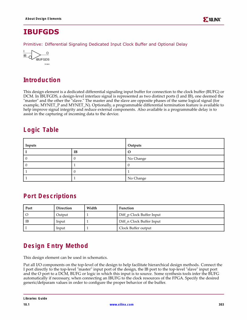
About Design Elements
IBUFGDS
Primitive: Differential Signaling Dedicated Input Clock Buffer and Optional Delay
IntroductionThis design element is a dedicated differential signaling input buffer for connection to the clock buffer (BUFG) orDCM. In IBUFGDS, a design-level interface signal is represented as two distinct ports (I and IB), one deemed the"master" and the other the "slave." The master and the slave are opposite phases of the same logical signal (forexample, MYNET_P and MYNET_N). Optionally, a programmable differential termination feature is available tohelp improve signal integrity and reduce external components. Also available is a programmable delay is toassist in the capturing of incoming data to the device.
Logic Table
Inputs Outputs
I IB O
0 0 No Change
0 1 0
1 0 1
1 1 No Change
Port DescriptionsPort Direction Width Function
O Output 1 Diff_p Clock Buffer Input
IB Input 1 Diff_n Clock Buffer Input
I Input 1 Clock Buffer output
Design Entry MethodThis design element can be used in schematics.
Put all I/O components on the top-level of the design to help facilitate hierarchical design methods. Connect theI port directly to the top-level "master" input port of the design, the IB port to the top-level "slave" input portand the O port to a DCM, BUFG or logic in which this input is to source. Some synthesis tools infer the BUFGautomatically if necessary, when connecting an IBUFG to the clock resources of the FPGA. Specify the desiredgeneric/defparam values in order to configure the proper behavior of the buffer.
Libraries Guide
10.1 www.xilinx.com 303
About Design Elements
Available AttributesAttribute Type Allowed Values Default Description
CAPACITANCE String "LOW","NORMAL","DONT_CARE"
"DONT_ CARE" Specified whether the I/O should beused with lower or normal intrinsiccapacitance.
DIFF_TERM Boolean TRUE or FALSE FALSE Enables the built-in differentialtermination resistor.
IOSTANDARD String See Data Sheet "DEFAULT" Assigns an I/O standard to theelement.
Libraries Guide
304 www.xilinx.com 10.1

About Design Elements
For More Information• See the Virtex-4 User Guide.
• See the Virtex-4 Data Sheets.
Libraries Guide
10.1 www.xilinx.com 305
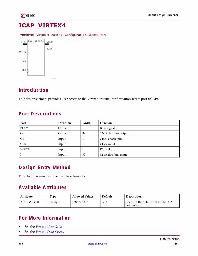
About Design Elements
ICAP_VIRTEX4
Primitive: Virtex-4 Internal Configuration Access Port
IntroductionThis design element provides user access to the Virtex-4 internal configuration access port (ICAP).
Port DescriptionsPort Direction Width Function
BUSY Output 1 Busy signal
O Output 32 32-bit data bus output
CE Input 1 Clock enable pin
CLK Input 1 Clock input
WRITE Input 1 Write signal
I Input 32 32-bit data bus input
Design Entry MethodThis design element can be used in schematics.
Available AttributesAttribute Type Allowed Values Default Description
ICAP_WIDTH String "X8" or "X32” "X8” Specifies the data width for the ICAPcomponent.
For More Information• See the Virtex-4 User Guide.• See the Virtex-4 Data Sheets.
Libraries Guide
306 www.xilinx.com 10.1
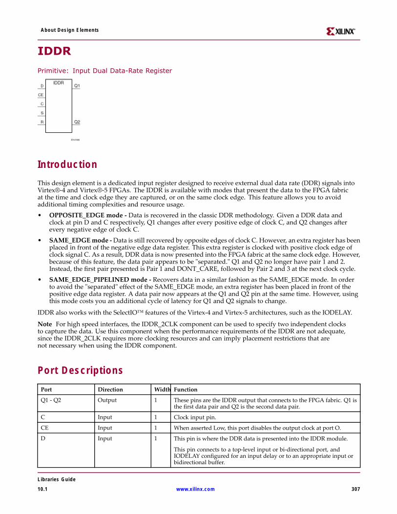
About Design Elements
IDDR
Primitive: Input Dual Data-Rate Register
IntroductionThis design element is a dedicated input register designed to receive external dual data rate (DDR) signals intoVirtex®-4 and Virtex®-5 FPGAs. The IDDR is available with modes that present the data to the FPGA fabricat the time and clock edge they are captured, or on the same clock edge. This feature allows you to avoidadditional timing complexities and resource usage.• OPPOSITE_EDGE mode - Data is recovered in the classic DDR methodology. Given a DDR data and
clock at pin D and C respectively, Q1 changes after every positive edge of clock C, and Q2 changes afterevery negative edge of clock C.
• SAME_EDGEmode -Data is still recovered by opposite edges of clock C. However, an extra register has beenplaced in front of the negative edge data register. This extra register is clocked with positive clock edge ofclock signal C. As a result, DDR data is now presented into the FPGA fabric at the same clock edge. However,because of this feature, the data pair appears to be "separated." Q1 and Q2 no longer have pair 1 and 2.Instead, the first pair presented is Pair 1 and DONT_CARE, followed by Pair 2 and 3 at the next clock cycle.
• SAME_EDGE_PIPELINED mode - Recovers data in a similar fashion as the SAME_EDGE mode. In orderto avoid the "separated" effect of the SAME_EDGE mode, an extra register has been placed in front of thepositive edge data register. A data pair now appears at the Q1 and Q2 pin at the same time. However, usingthis mode costs you an additional cycle of latency for Q1 and Q2 signals to change.
IDDR also works with the SelectIO™ features of the Virtex-4 and Virtex-5 architectures, such as the IODELAY.
Note For high speed interfaces, the IDDR_2CLK component can be used to specify two independent clocksto capture the data. Use this component when the performance requirements of the IDDR are not adequate,since the IDDR_2CLK requires more clocking resources and can imply placement restrictions that arenot necessary when using the IDDR component.
Port DescriptionsPort Direction Width Function
Q1 - Q2 Output 1 These pins are the IDDR output that connects to the FPGA fabric. Q1 isthe first data pair and Q2 is the second data pair.
C Input 1 Clock input pin.
CE Input 1 When asserted Low, this port disables the output clock at port O.
D Input 1 This pin is where the DDR data is presented into the IDDR module.
This pin connects to a top-level input or bi-directional port, andIODELAY configured for an input delay or to an appropriate input orbidirectional buffer.
Libraries Guide
10.1 www.xilinx.com 307
About Design Elements
Port Direction Width Function
R Input 1 Active high reset forcing Q1 and Q2 to a logic zero. Can be synchronousor asynchronous based on the SRTYPE attribute.
S Input 1 Active high reset forcing Q1 and Q2 to a logic one. Can be synchronousor asynchronous based on the SRTYPE attribute.
Design Entry MethodThis design element can be used in schematics.
Available AttributesAttribute Type Allowed Values Default Description
DDR_CLK_EDGE
String "OPPOSITE_ EDGE","SAME_EDG E","SAME_EDGE_PIPELINED"
"OPPOSITE_EDGE”
DDR clock mode recovery mode selection.See below for more explanation.
INIT_Q1 Binary 0 or 1 0 Initial value on the Q1 pin afterconfiguration startup or when GSR isasserted.
INIT_Q2 Binary 0 or 1 0 Initial value on the Q2 pin afterconfiguration startup or when GSR isasserted.
SRTYPE String "SYNC" or "ASYNC” "SYNC” Set/reset type selection. "SYNC" specifiesthe behavior of the reset (R) and set (S)pins to be synchronous to the positive edgeof the C clock pin. "ASYNC" specifies anasynchronous set/reset function.
For More Information• See the Virtex-4 User Guide.
• See the Virtex-4 Data Sheets.
Libraries Guide
308 www.xilinx.com 10.1
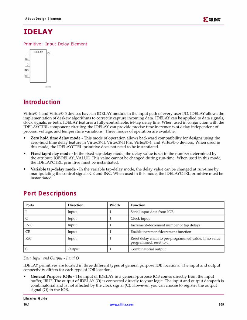
About Design Elements
IDELAY
Primitive: Input Delay Element
IntroductionVirtex®-4 and Virtex®-5 devices have an IDELAY module in the input path of every user I/O. IDELAY allows theimplementation of deskew algorithms to correctly capture incoming data. IDELAY can be applied to data signals,clock signals, or both. IDELAY features a fully-controllable, 64-tap delay line. When used in conjunction with theIDELAYCTRL component circuitry, the IDELAY can provide precise time increments of delay independent ofprocess, voltage, and temperature variations. Three modes of operation are available:• Zero hold time delay mode - This mode of operation allows backward compatibility for designs using the
zero-hold time delay feature in Virtex®-II, Virtex®-II Pro, Virtex®-4, and Virtex®-5 devices. When used inthis mode, the IDELAYCTRL primitive does not need to be instantiated.
• Fixed tap-delay mode - In the fixed tap-delay mode, the delay value is set to the number determined bythe attribute IOBDELAY_VALUE. This value cannot be changed during run-time. When used in this mode,the IDELAYCTRL primitive must be instantiated.
• Variable tap-delay mode - In the variable tap-delay mode, the delay value can be changed at run-time bymanipulating the control signals CE and INC. When used in this mode, the IDELAYCTRL primitive must beinstantiated.
Port DescriptionsPorts Direction Width Function
I Input 1 Serial input data from IOB
C Input 1 Clock input
INC Input 1 Increment/decrement number of tap delays
CE Input 1 Enable increment/decrement function
RST Input 1 Reset delay chain to pre-programmed value. If no valueprogrammed, reset to 0.
O Output 1 Combinatorial output
Data Input and Output - I and O
IDELAY primitives are located in three different types of general purpose IOB locations. The input and outputconnectivity differs for each type of IOB location.• General Purpose IOBs - The input of IDELAY in a general-purpose IOB comes directly from the input
buffer, IBUF. The output of IDELAY (O) is connected directly to your logic. The input and output datapath iscombinatorial and is not affected by the clock signal (C). However, you can choose to register the outputsignal (O) in the IOB.
Libraries Guide
10.1 www.xilinx.com 309
About Design Elements
• Regional Clock-Capable IOBs - Regional clock-capable IOBs are located in one I/O pair directly above andbelow an HCLK IOB. The input of IDELAY in a regional clock-capable IOB comes directly from the inputbuffer, IBUF. The output of IDELAY in a regional clock-capable IOB can go to one of the following locations:– Directly to your logic– BUFIO (in the case of a regional clock signal)The regional clock buffer, BUFIO, connects the incoming regional clock signal to the regional I/O clock tree,IOCLK. BUFIO also connects to the regional clock buffer, BUFR to connect to the regional clock tree, rclk.The input and output datapath is combinatorial and is not affected by the clock signal (C). However, you canchoose to register the output signal (O) in the IOB.
• Global clock-capable IOBs - Global clock-capable IOBs are located in the center I/O column. The input ofthe IDELAY module in a global clock-capable IOB comes directly from the input global clock buffer, IBUFG.The output of the IDELAY module in a global clock-capable IOB can go to one of the following locations:– Directly to your logic– BUFG (in the case of a global clock signal)The global clock buffer, BUFG, connects the incoming regional clock signal to the global clock tree, gclk. Theinput and output datapath is combinatorial and is not affected by the clock signal (C). However, you canchoose to register the output signal (O) in the IOB.
Clock Input - C
All control inputs to IDELAY (RST, CE and INC) are synchronous to the clock input (C). The data input andoutput (I and O) of IDELAY is not affected by this clock signal. This clock input is identical to the CLKDIV inputfor the ISERDES. All the clock sources used to drive CLKDIV can therefore drive the IDELAY clock input (C).The clock sources that can drive the clock input (C) are:• Eight gclk (global clock tree)• Two rclk (regional clock tree)
Module Reset - RST
The IDELAY reset signal, RST, resets the tap-delay line to a value set by the IOBDELAY_VALUE attribute. If theIOBDELAY_VALUE attribute is not specified, the tap-delay line is reset to 0.
Increment/Decrement Signals - CE, INC
The increment/decrement enable signal (CE) determines when the increment/decrement signal (INC) isactivated. INC determines whether to increment or decrement the tap-delay line. When CE = 0, the tap delayremains constant no matter what the value of INC. When CE = 1, the tap-delay value increments or decrementsdepending on the value of INC. The tap delay is incremented or decremented synchronously with respect tothe input clock (C). As long as CE = 1, the tap-delay increments or decrements by one every clock cycle. Theincrement/decrement operation is summarized in the following table:
Operation RST CE INC
Reset to configured value oftap count
1 x x
Increment tap count 0 1 1
Decrement tap count 0 1 0
No change 0 0 x
Note1. RST resets delay chain to tap count specified by attribute IOBDELAY_VALUE. If IOBDELAY_VALUE
is not specified, tap count reset to 0.2. RST, CE, and INC are synchronous to the input clock signal (C).
When CE is raised, the increment/decrement operation begins on the next positive clock cycle. When CE islowered, the increment/decrement operation ceases on the next positive clock cycle.
Libraries Guide
310 www.xilinx.com 10.1
About Design Elements
Design Entry MethodThis design element can be used in schematics.
Available AttributesAttribute Type Allowed Values Default Description
IOBDELAY_TYPE String “DEFAULT”,“FIXED”,or “VARIABLE”
“DEFAULT” This attribute sets the type of tapdelay.
IOBDELAY_VALUE Integer 0 to 63 0 This attribute specifies the initialnumber of tap delays.
IOBDELAY_TYPE Attribute
The IOBDELAY_TYPE attribute sets the type of delay used. The attribute values are DEFAULT, FIXED, andVARIABLE. The default value is DEFAULT. When set to DEFAULT, the zero-hold time delay element is selected.This delay element eliminates pad-to-pad hold time. The delay is matched to the internal clock-distributiondelay of the device. When used, it guarantees a pad-to-pad hold time of zero.
When set to FIXED, the tap-delay value is fixed at the number of taps determined by the IOBDELAY_VALUEattribute. This value is preset and cannot be changed dynamically.
When set to VARIABLE, the variable tap delay is selected. The tap delay can be incremented by setting CE =1and INC = 1 or decremented by setting CE = 1 and INC = 0. The increment/decrement operation is synchronousto C, the input clock signal.
IOBDELAY_VALUE Attribute
The IOBDELAY_VALUE attribute specifies the initial number of tap delays. The possible values are any Integersfrom 0 to 63. The default value is 0. When set to 0, the total delay becomes the delay of the output MUX which isapproximately 400 ps.
The value of the tap delay reverts to IOBDELAY_VALUE when the tap delay is reset (RST = 1), or theIOBDELAY_TYPE is set to FIXED.
For More Information• See the Virtex-4 User Guide.
• See the Virtex-4 Data Sheets.
Libraries Guide
10.1 www.xilinx.com 311
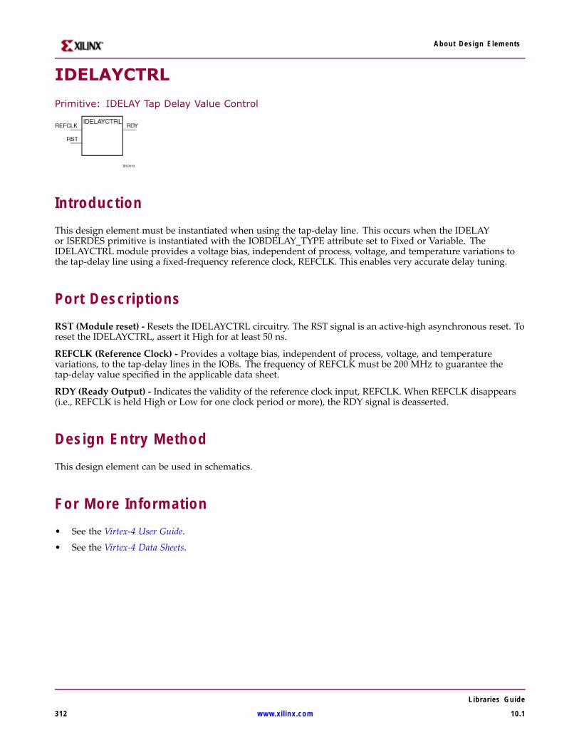
About Design Elements
IDELAYCTRL
Primitive: IDELAY Tap Delay Value Control
IntroductionThis design element must be instantiated when using the tap-delay line. This occurs when the IDELAYor ISERDES primitive is instantiated with the IOBDELAY_TYPE attribute set to Fixed or Variable. TheIDELAYCTRL module provides a voltage bias, independent of process, voltage, and temperature variations tothe tap-delay line using a fixed-frequency reference clock, REFCLK. This enables very accurate delay tuning.
Port DescriptionsRST (Module reset) - Resets the IDELAYCTRL circuitry. The RST signal is an active-high asynchronous reset. Toreset the IDELAYCTRL, assert it High for at least 50 ns.
REFCLK (Reference Clock) - Provides a voltage bias, independent of process, voltage, and temperaturevariations, to the tap-delay lines in the IOBs. The frequency of REFCLK must be 200 MHz to guarantee thetap-delay value specified in the applicable data sheet.
RDY (Ready Output) - Indicates the validity of the reference clock input, REFCLK. When REFCLK disappears(i.e., REFCLK is held High or Low for one clock period or more), the RDY signal is deasserted.
Design Entry MethodThis design element can be used in schematics.
For More Information• See the Virtex-4 User Guide.
• See the Virtex-4 Data Sheets.
Libraries Guide
312 www.xilinx.com 10.1
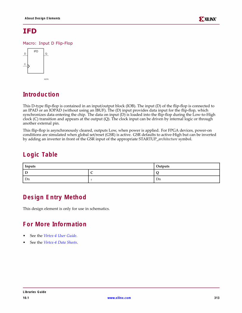
About Design Elements
IFD
Macro: Input D Flip-Flop
IntroductionThis D-type flip-flop is contained in an input/output block (IOB). The input (D) of the flip-flop is connected toan IPAD or an IOPAD (without using an IBUF). The (D) input provides data input for the flip-flop, whichsynchronizes data entering the chip. The data on input (D) is loaded into the flip-flop during the Low-to-Highclock (C) transition and appears at the output (Q). The clock input can be driven by internal logic or throughanother external pin.
This flip-flop is asynchronously cleared, outputs Low, when power is applied. For FPGA devices, power-onconditions are simulated when global set/reset (GSR) is active. GSR defaults to active-High but can be invertedby adding an inverter in front of the GSR input of the appropriate STARTUP_architecture symbol.
Logic TableInputs Outputs
D C Q
Dn ↑ Dn
Design Entry MethodThis design element is only for use in schematics.
For More Information• See the Virtex-4 User Guide.
• See the Virtex-4 Data Sheets.
Libraries Guide
10.1 www.xilinx.com 313
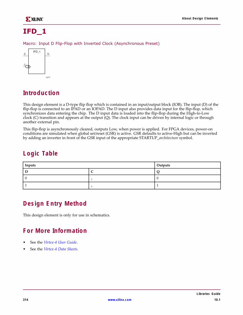
About Design Elements
IFD_1
Macro: Input D Flip-Flop with Inverted Clock (Asynchronous Preset)
IntroductionThis design element is a D-type flip flop which is contained in an input/output block (IOB). The input (D) of theflip-flop is connected to an IPAD or an IOPAD. The D input also provides data input for the flip-flop, whichsynchronizes data entering the chip. The D input data is loaded into the flip-flop during the High-to-Lowclock (C) transition and appears at the output (Q). The clock input can be driven by internal logic or throughanother external pin.
This flip-flop is asynchronously cleared, outputs Low, when power is applied. For FPGA devices, power-onconditions are simulated when global set/reset (GSR) is active. GSR defaults to active-High but can be invertedby adding an inverter in front of the GSR input of the appropriate STARTUP_architecture symbol.
Logic TableInputs Outputs
D C Q
0 ↓ 0
1 ↓ 1
Design Entry MethodThis design element is only for use in schematics.
For More Information• See the Virtex-4 User Guide.
• See the Virtex-4 Data Sheets.
Libraries Guide
314 www.xilinx.com 10.1

About Design Elements
IFD16
Macro: 16-Bit Input D Flip-Flop
IntroductionThis D-type flip-flop is contained in an input/output block (IOB). The input (D) of the flip-flop is connected toan IPAD or an IOPAD (without using an IBUF). The (D) input provides data input for the flip-flop, whichsynchronizes data entering the chip. The data on input (D) is loaded into the flip-flop during the Low-to-Highclock (C) transition and appears at the output (Q). The clock input can be driven by internal logic or throughanother external pin.
This flip-flop is asynchronously cleared, outputs Low, when power is applied. For FPGA devices, power-onconditions are simulated when global set/reset (GSR) is active. GSR defaults to active-High but can be invertedby adding an inverter in front of the GSR input of the appropriate STARTUP_architecture symbol.
Logic TableInputs Outputs
D C Q
Dn ↑ Dn
Design Entry MethodThis design element is only for use in schematics.
For More Information• See the Virtex-4 User Guide.
• See the Virtex-4 Data Sheets.
Libraries Guide
10.1 www.xilinx.com 315
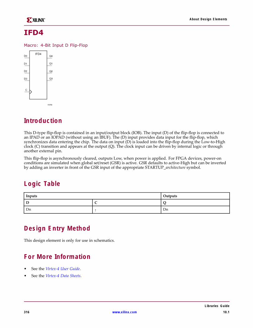
About Design Elements
IFD4
Macro: 4-Bit Input D Flip-Flop
IntroductionThis D-type flip-flop is contained in an input/output block (IOB). The input (D) of the flip-flop is connected toan IPAD or an IOPAD (without using an IBUF). The (D) input provides data input for the flip-flop, whichsynchronizes data entering the chip. The data on input (D) is loaded into the flip-flop during the Low-to-Highclock (C) transition and appears at the output (Q). The clock input can be driven by internal logic or throughanother external pin.
This flip-flop is asynchronously cleared, outputs Low, when power is applied. For FPGA devices, power-onconditions are simulated when global set/reset (GSR) is active. GSR defaults to active-High but can be invertedby adding an inverter in front of the GSR input of the appropriate STARTUP_architecture symbol.
Logic TableInputs Outputs
D C Q
Dn ↑ Dn
Design Entry MethodThis design element is only for use in schematics.
For More Information• See the Virtex-4 User Guide.
• See the Virtex-4 Data Sheets.
Libraries Guide
316 www.xilinx.com 10.1
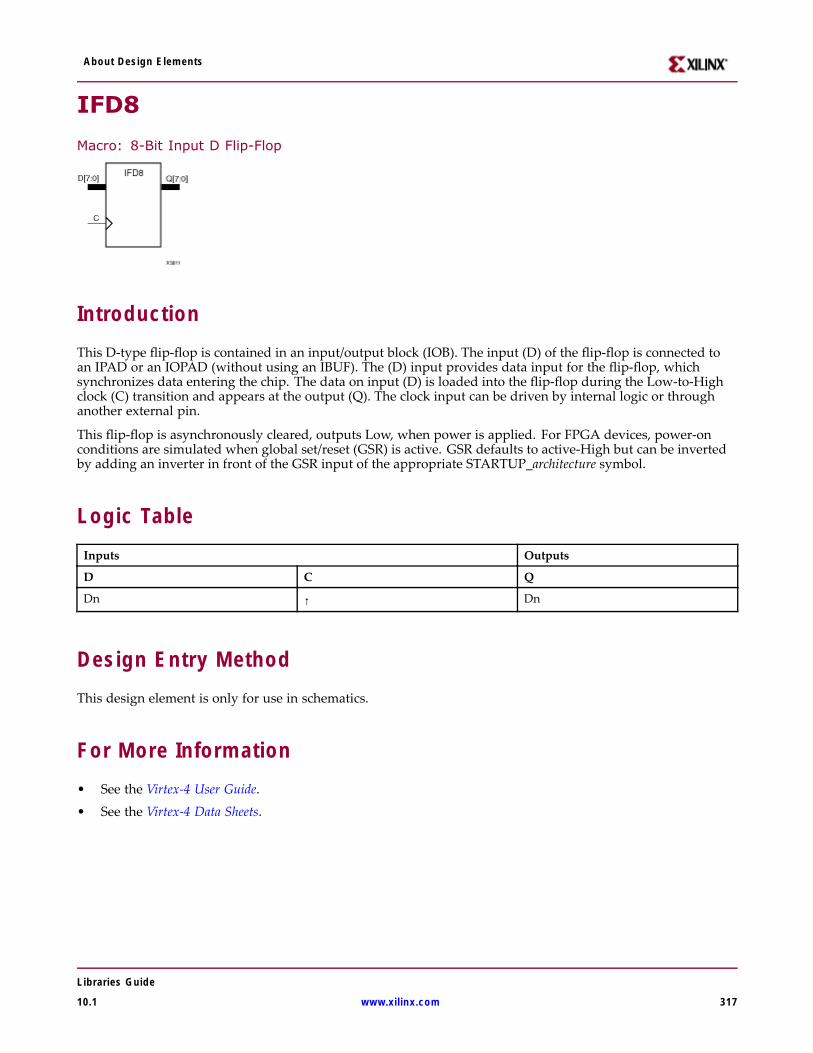
About Design Elements
IFD8
Macro: 8-Bit Input D Flip-Flop
IntroductionThis D-type flip-flop is contained in an input/output block (IOB). The input (D) of the flip-flop is connected toan IPAD or an IOPAD (without using an IBUF). The (D) input provides data input for the flip-flop, whichsynchronizes data entering the chip. The data on input (D) is loaded into the flip-flop during the Low-to-Highclock (C) transition and appears at the output (Q). The clock input can be driven by internal logic or throughanother external pin.
This flip-flop is asynchronously cleared, outputs Low, when power is applied. For FPGA devices, power-onconditions are simulated when global set/reset (GSR) is active. GSR defaults to active-High but can be invertedby adding an inverter in front of the GSR input of the appropriate STARTUP_architecture symbol.
Logic TableInputs Outputs
D C Q
Dn ↑ Dn
Design Entry MethodThis design element is only for use in schematics.
For More Information• See the Virtex-4 User Guide.
• See the Virtex-4 Data Sheets.
Libraries Guide
10.1 www.xilinx.com 317
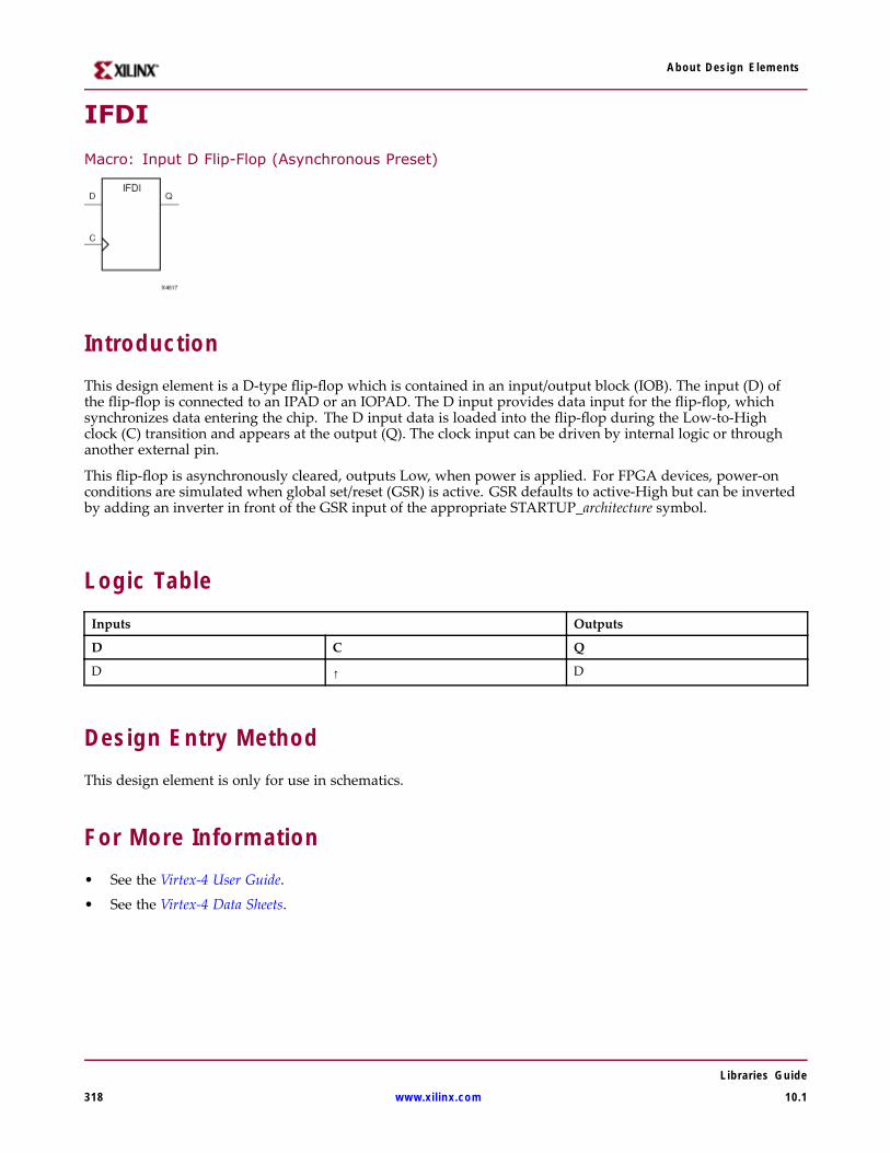
About Design Elements
IFDI
Macro: Input D Flip-Flop (Asynchronous Preset)
IntroductionThis design element is a D-type flip-flop which is contained in an input/output block (IOB). The input (D) ofthe flip-flop is connected to an IPAD or an IOPAD. The D input provides data input for the flip-flop, whichsynchronizes data entering the chip. The D input data is loaded into the flip-flop during the Low-to-Highclock (C) transition and appears at the output (Q). The clock input can be driven by internal logic or throughanother external pin.
This flip-flop is asynchronously cleared, outputs Low, when power is applied. For FPGA devices, power-onconditions are simulated when global set/reset (GSR) is active. GSR defaults to active-High but can be invertedby adding an inverter in front of the GSR input of the appropriate STARTUP_architecture symbol.
Logic TableInputs Outputs
D C Q
D ↑ D
Design Entry MethodThis design element is only for use in schematics.
For More Information• See the Virtex-4 User Guide.
• See the Virtex-4 Data Sheets.
Libraries Guide
318 www.xilinx.com 10.1
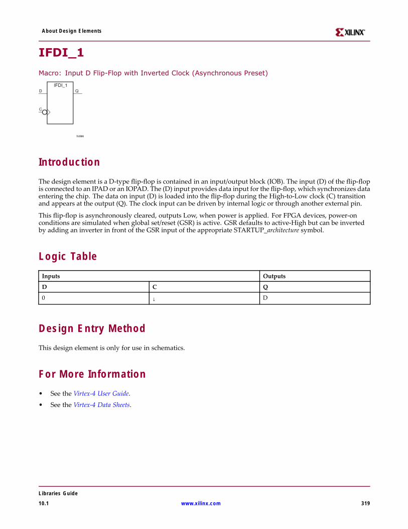
About Design Elements
IFDI_1
Macro: Input D Flip-Flop with Inverted Clock (Asynchronous Preset)
IntroductionThe design element is a D-type flip-flop is contained in an input/output block (IOB). The input (D) of the flip-flopis connected to an IPAD or an IOPAD. The (D) input provides data input for the flip-flop, which synchronizes dataentering the chip. The data on input (D) is loaded into the flip-flop during the High-to-Low clock (C) transitionand appears at the output (Q). The clock input can be driven by internal logic or through another external pin.
This flip-flop is asynchronously cleared, outputs Low, when power is applied. For FPGA devices, power-onconditions are simulated when global set/reset (GSR) is active. GSR defaults to active-High but can be invertedby adding an inverter in front of the GSR input of the appropriate STARTUP_architecture symbol.
Logic TableInputs Outputs
D C Q
0 ↓ D
Design Entry MethodThis design element is only for use in schematics.
For More Information• See the Virtex-4 User Guide.
• See the Virtex-4 Data Sheets.
Libraries Guide
10.1 www.xilinx.com 319
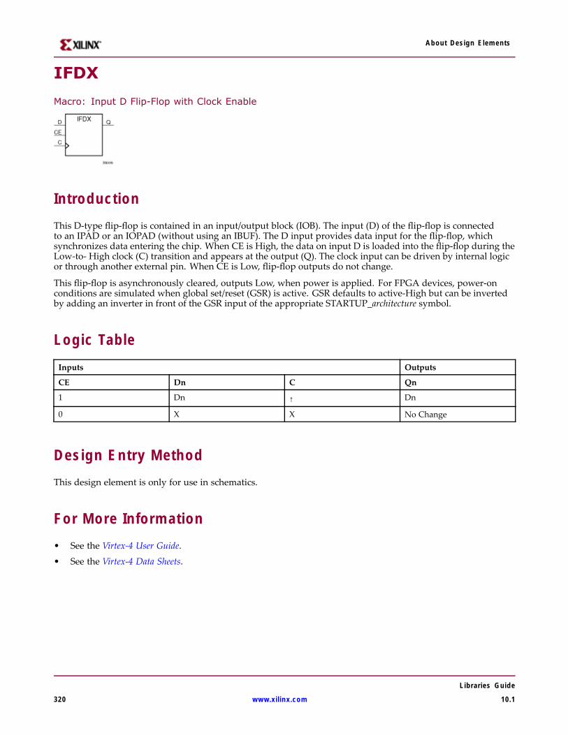
About Design Elements
IFDX
Macro: Input D Flip-Flop with Clock Enable
IntroductionThis D-type flip-flop is contained in an input/output block (IOB). The input (D) of the flip-flop is connectedto an IPAD or an IOPAD (without using an IBUF). The D input provides data input for the flip-flop, whichsynchronizes data entering the chip. When CE is High, the data on input D is loaded into the flip-flop during theLow-to- High clock (C) transition and appears at the output (Q). The clock input can be driven by internal logicor through another external pin. When CE is Low, flip-flop outputs do not change.
This flip-flop is asynchronously cleared, outputs Low, when power is applied. For FPGA devices, power-onconditions are simulated when global set/reset (GSR) is active. GSR defaults to active-High but can be invertedby adding an inverter in front of the GSR input of the appropriate STARTUP_architecture symbol.
Logic TableInputs Outputs
CE Dn C Qn
1 Dn ↑ Dn
0 X X No Change
Design Entry MethodThis design element is only for use in schematics.
For More Information• See the Virtex-4 User Guide.
• See the Virtex-4 Data Sheets.
Libraries Guide
320 www.xilinx.com 10.1
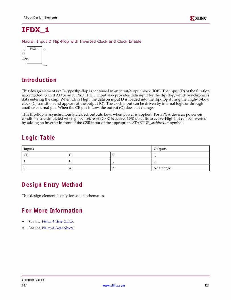
About Design Elements
IFDX_1
Macro: Input D Flip-Flop with Inverted Clock and Clock Enable
IntroductionThis design element is a D-type flip-flop is contained in an input/output block (IOB). The input (D) of the flip-flopis connected to an IPAD or an IOPAD. The D input also provides data input for the flip-flop, which synchronizesdata entering the chip. When CE is High, the data on input D is loaded into the flip-flop during the High-to-Lowclock (C) transition and appears at the output (Q). The clock input can be driven by internal logic or throughanother external pin. When the CE pin is Low, the output (Q) does not change.
This flip-flop is asynchronously cleared, outputs Low, when power is applied. For FPGA devices, power-onconditions are simulated when global set/reset (GSR) is active. GSR defaults to active-High but can be invertedby adding an inverter in front of the GSR input of the appropriate STARTUP_architecture symbol.
Logic TableInputs Outputs
CE D C Q
1 D ↓ D
0 X X No Change
Design Entry MethodThis design element is only for use in schematics.
For More Information• See the Virtex-4 User Guide.
• See the Virtex-4 Data Sheets.
Libraries Guide
10.1 www.xilinx.com 321
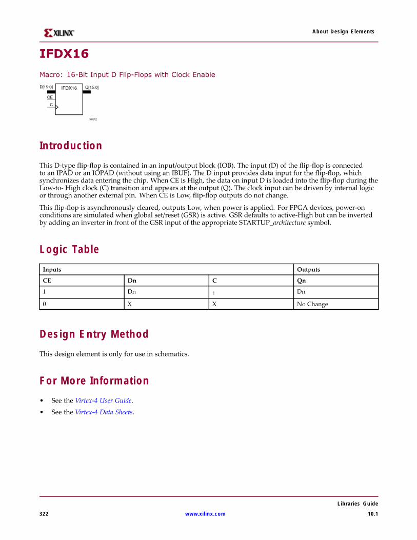
About Design Elements
IFDX16
Macro: 16-Bit Input D Flip-Flops with Clock Enable
IntroductionThis D-type flip-flop is contained in an input/output block (IOB). The input (D) of the flip-flop is connectedto an IPAD or an IOPAD (without using an IBUF). The D input provides data input for the flip-flop, whichsynchronizes data entering the chip. When CE is High, the data on input D is loaded into the flip-flop during theLow-to- High clock (C) transition and appears at the output (Q). The clock input can be driven by internal logicor through another external pin. When CE is Low, flip-flop outputs do not change.
This flip-flop is asynchronously cleared, outputs Low, when power is applied. For FPGA devices, power-onconditions are simulated when global set/reset (GSR) is active. GSR defaults to active-High but can be invertedby adding an inverter in front of the GSR input of the appropriate STARTUP_architecture symbol.
Logic TableInputs Outputs
CE Dn C Qn
1 Dn ↑ Dn
0 X X No Change
Design Entry MethodThis design element is only for use in schematics.
For More Information• See the Virtex-4 User Guide.
• See the Virtex-4 Data Sheets.
Libraries Guide
322 www.xilinx.com 10.1
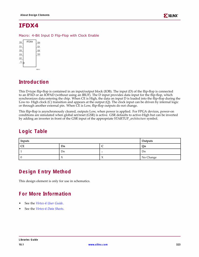
About Design Elements
IFDX4
Macro: 4-Bit Input D Flip-Flop with Clock Enable
IntroductionThis D-type flip-flop is contained in an input/output block (IOB). The input (D) of the flip-flop is connectedto an IPAD or an IOPAD (without using an IBUF). The D input provides data input for the flip-flop, whichsynchronizes data entering the chip. When CE is High, the data on input D is loaded into the flip-flop during theLow-to- High clock (C) transition and appears at the output (Q). The clock input can be driven by internal logicor through another external pin. When CE is Low, flip-flop outputs do not change.
This flip-flop is asynchronously cleared, outputs Low, when power is applied. For FPGA devices, power-onconditions are simulated when global set/reset (GSR) is active. GSR defaults to active-High but can be invertedby adding an inverter in front of the GSR input of the appropriate STARTUP_architecture symbol.
Logic TableInputs Outputs
CE Dn C Qn
1 Dn ↑ Dn
0 X X No Change
Design Entry MethodThis design element is only for use in schematics.
For More Information• See the Virtex-4 User Guide.
• See the Virtex-4 Data Sheets.
Libraries Guide
10.1 www.xilinx.com 323
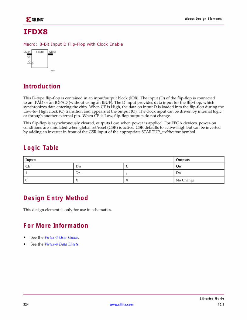
About Design Elements
IFDX8
Macro: 8-Bit Input D Flip-Flop with Clock Enable
IntroductionThis D-type flip-flop is contained in an input/output block (IOB). The input (D) of the flip-flop is connectedto an IPAD or an IOPAD (without using an IBUF). The D input provides data input for the flip-flop, whichsynchronizes data entering the chip. When CE is High, the data on input D is loaded into the flip-flop during theLow-to- High clock (C) transition and appears at the output (Q). The clock input can be driven by internal logicor through another external pin. When CE is Low, flip-flop outputs do not change.
This flip-flop is asynchronously cleared, outputs Low, when power is applied. For FPGA devices, power-onconditions are simulated when global set/reset (GSR) is active. GSR defaults to active-High but can be invertedby adding an inverter in front of the GSR input of the appropriate STARTUP_architecture symbol.
Logic TableInputs Outputs
CE Dn C Qn
1 Dn ↑ Dn
0 X X No Change
Design Entry MethodThis design element is only for use in schematics.
For More Information• See the Virtex-4 User Guide.
• See the Virtex-4 Data Sheets.
Libraries Guide
324 www.xilinx.com 10.1
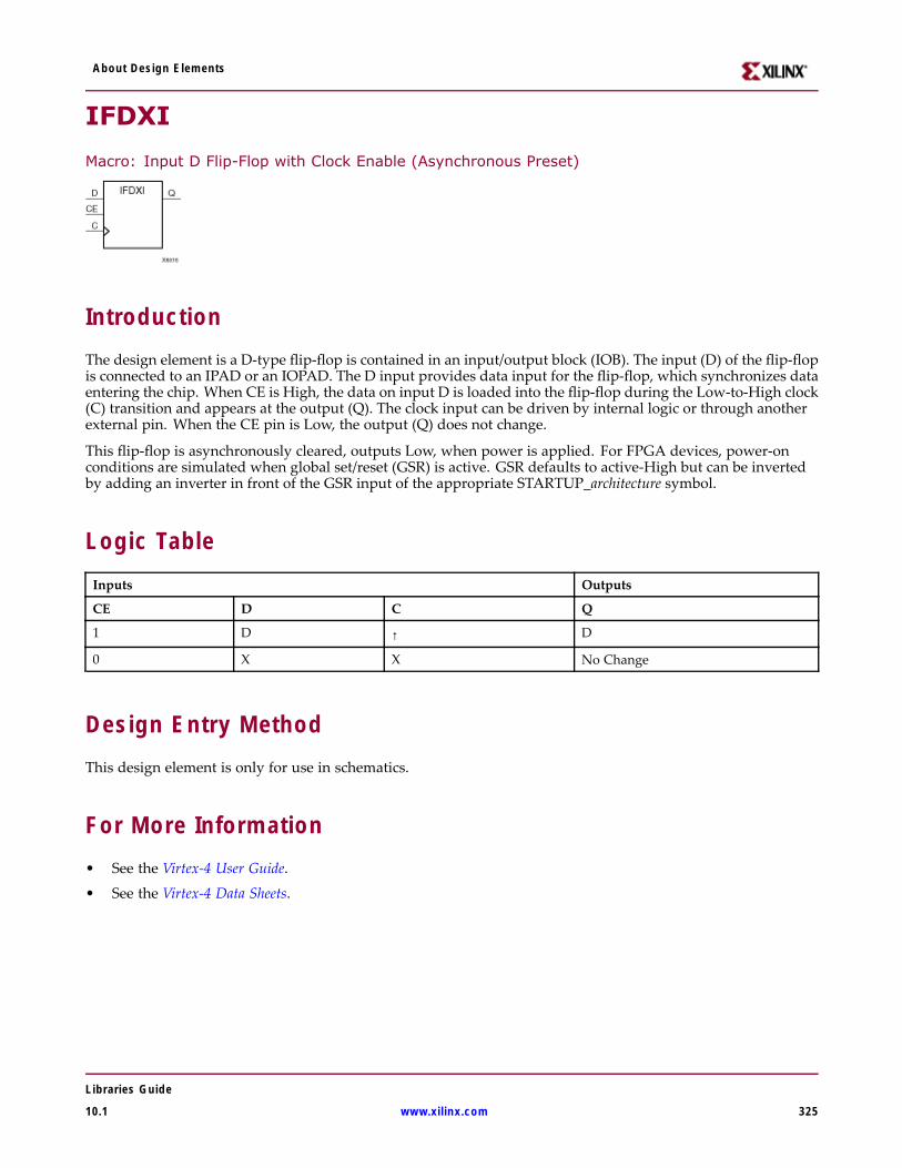
About Design Elements
IFDXI
Macro: Input D Flip-Flop with Clock Enable (Asynchronous Preset)
IntroductionThe design element is a D-type flip-flop is contained in an input/output block (IOB). The input (D) of the flip-flopis connected to an IPAD or an IOPAD. The D input provides data input for the flip-flop, which synchronizes dataentering the chip. When CE is High, the data on input D is loaded into the flip-flop during the Low-to-High clock(C) transition and appears at the output (Q). The clock input can be driven by internal logic or through anotherexternal pin. When the CE pin is Low, the output (Q) does not change.
This flip-flop is asynchronously cleared, outputs Low, when power is applied. For FPGA devices, power-onconditions are simulated when global set/reset (GSR) is active. GSR defaults to active-High but can be invertedby adding an inverter in front of the GSR input of the appropriate STARTUP_architecture symbol.
Logic TableInputs Outputs
CE D C Q
1 D ↑ D
0 X X No Change
Design Entry MethodThis design element is only for use in schematics.
For More Information• See the Virtex-4 User Guide.
• See the Virtex-4 Data Sheets.
Libraries Guide
10.1 www.xilinx.com 325
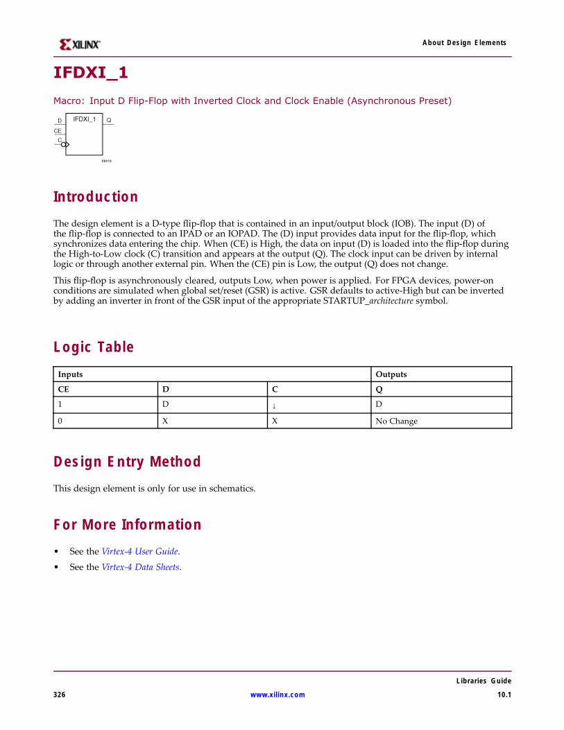
About Design Elements
IFDXI_1
Macro: Input D Flip-Flop with Inverted Clock and Clock Enable (Asynchronous Preset)
IntroductionThe design element is a D-type flip-flop that is contained in an input/output block (IOB). The input (D) ofthe flip-flop is connected to an IPAD or an IOPAD. The (D) input provides data input for the flip-flop, whichsynchronizes data entering the chip. When (CE) is High, the data on input (D) is loaded into the flip-flop duringthe High-to-Low clock (C) transition and appears at the output (Q). The clock input can be driven by internallogic or through another external pin. When the (CE) pin is Low, the output (Q) does not change.
This flip-flop is asynchronously cleared, outputs Low, when power is applied. For FPGA devices, power-onconditions are simulated when global set/reset (GSR) is active. GSR defaults to active-High but can be invertedby adding an inverter in front of the GSR input of the appropriate STARTUP_architecture symbol.
Logic TableInputs Outputs
CE D C Q
1 D ↓ D
0 X X No Change
Design Entry MethodThis design element is only for use in schematics.
For More Information• See the Virtex-4 User Guide.
• See the Virtex-4 Data Sheets.
Libraries Guide
326 www.xilinx.com 10.1
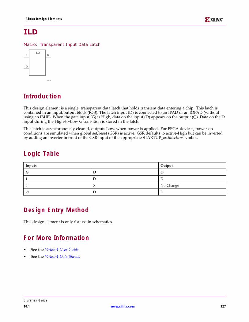
About Design Elements
ILD
Macro: Transparent Input Data Latch
IntroductionThis design element is a single, transparent data latch that holds transient data entering a chip. This latch iscontained in an input/output block (IOB). The latch input (D) is connected to an IPAD or an IOPAD (withoutusing an IBUF). When the gate input (G) is High, data on the input (D) appears on the output (Q). Data on the Dinput during the High-to-Low G transition is stored in the latch.
This latch is asynchronously cleared, outputs Low, when power is applied. For FPGA devices, power-onconditions are simulated when global set/reset (GSR) is active. GSR defaults to active-High but can be invertedby adding an inverter in front of the GSR input of the appropriate STARTUP_architecture symbol.
Logic TableInputs Output
G D Q
1 D D
0 X No Change
Ø D D
Design Entry MethodThis design element is only for use in schematics.
For More Information• See the Virtex-4 User Guide.
• See the Virtex-4 Data Sheets.
Libraries Guide
10.1 www.xilinx.com 327
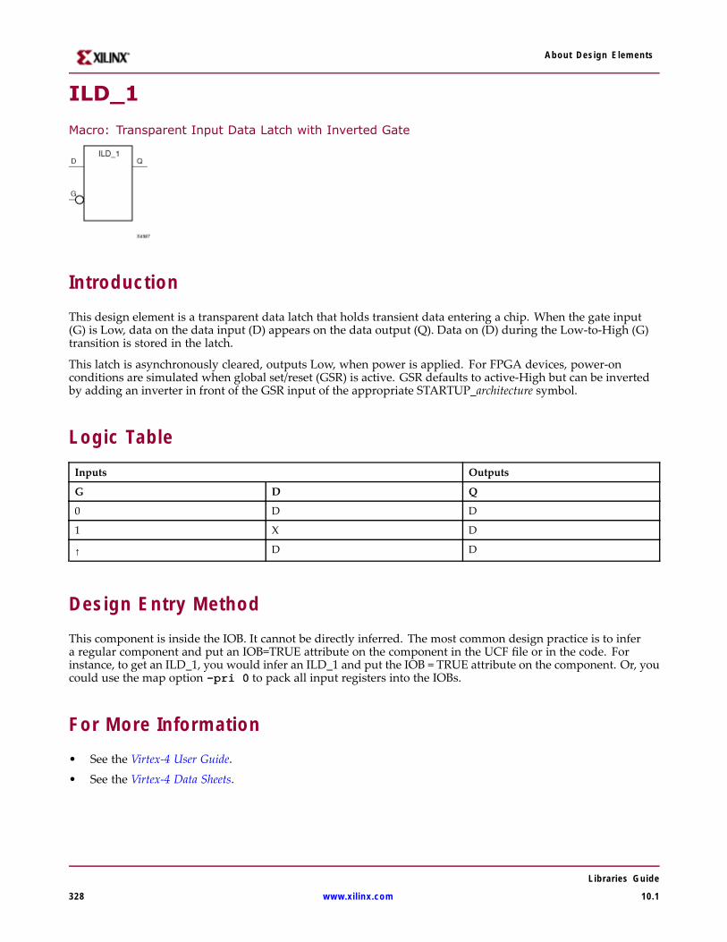
About Design Elements
ILD_1
Macro: Transparent Input Data Latch with Inverted Gate
IntroductionThis design element is a transparent data latch that holds transient data entering a chip. When the gate input(G) is Low, data on the data input (D) appears on the data output (Q). Data on (D) during the Low-to-High (G)transition is stored in the latch.
This latch is asynchronously cleared, outputs Low, when power is applied. For FPGA devices, power-onconditions are simulated when global set/reset (GSR) is active. GSR defaults to active-High but can be invertedby adding an inverter in front of the GSR input of the appropriate STARTUP_architecture symbol.
Logic TableInputs Outputs
G D Q
0 D D
1 X D
↑ D D
Design Entry MethodThis component is inside the IOB. It cannot be directly inferred. The most common design practice is to infera regular component and put an IOB=TRUE attribute on the component in the UCF file or in the code. Forinstance, to get an ILD_1, you would infer an ILD_1 and put the IOB = TRUE attribute on the component. Or, youcould use the map option –pri–pri–pri 000 to pack all input registers into the IOBs.
For More Information• See the Virtex-4 User Guide.
• See the Virtex-4 Data Sheets.
Libraries Guide
328 www.xilinx.com 10.1
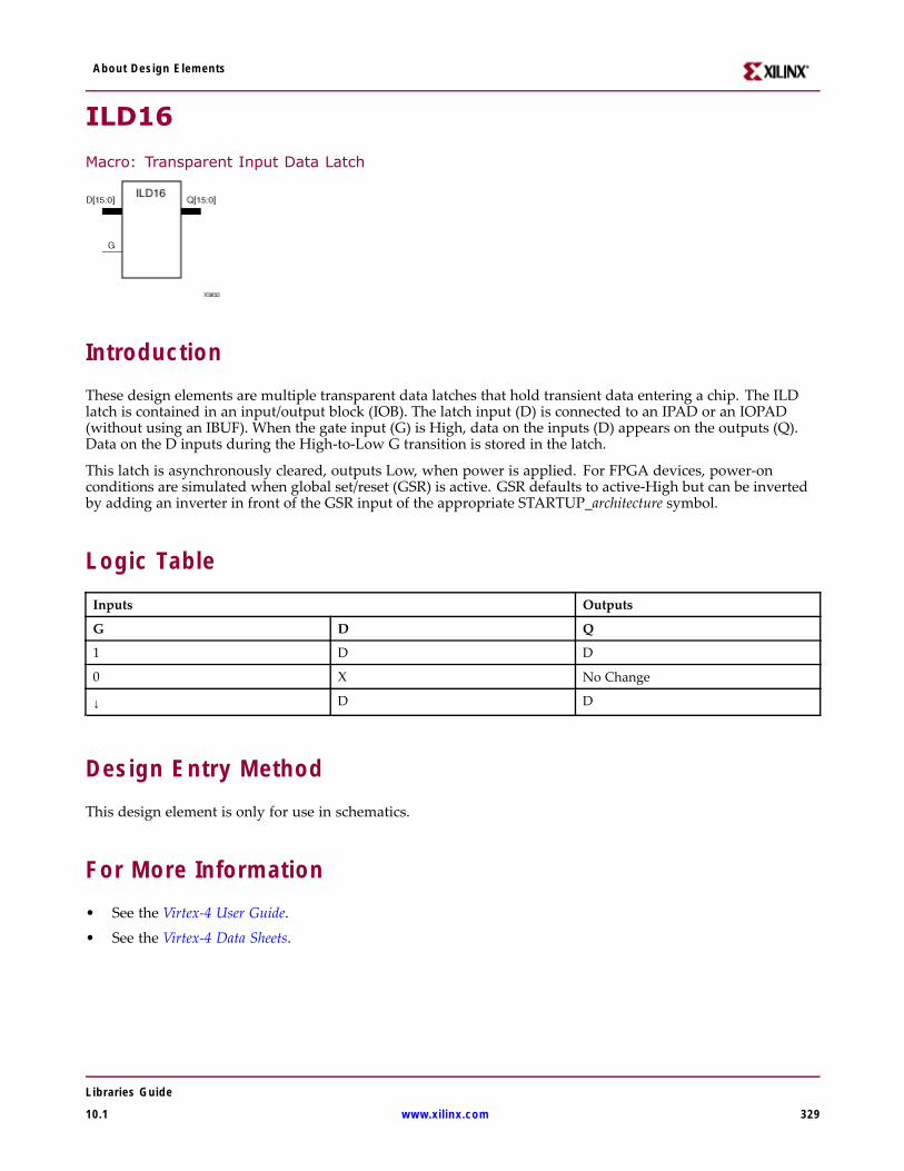
About Design Elements
ILD16
Macro: Transparent Input Data Latch
IntroductionThese design elements are multiple transparent data latches that hold transient data entering a chip. The ILDlatch is contained in an input/output block (IOB). The latch input (D) is connected to an IPAD or an IOPAD(without using an IBUF). When the gate input (G) is High, data on the inputs (D) appears on the outputs (Q).Data on the D inputs during the High-to-Low G transition is stored in the latch.
This latch is asynchronously cleared, outputs Low, when power is applied. For FPGA devices, power-onconditions are simulated when global set/reset (GSR) is active. GSR defaults to active-High but can be invertedby adding an inverter in front of the GSR input of the appropriate STARTUP_architecture symbol.
Logic TableInputs Outputs
G D Q
1 D D
0 X No Change
↓ D D
Design Entry MethodThis design element is only for use in schematics.
For More Information• See the Virtex-4 User Guide.
• See the Virtex-4 Data Sheets.
Libraries Guide
10.1 www.xilinx.com 329
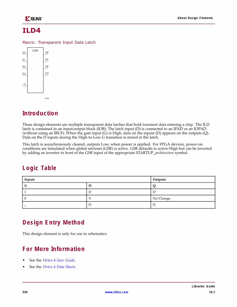
About Design Elements
ILD4
Macro: Transparent Input Data Latch
IntroductionThese design elements are multiple transparent data latches that hold transient data entering a chip. The ILDlatch is contained in an input/output block (IOB). The latch input (D) is connected to an IPAD or an IOPAD(without using an IBUF). When the gate input (G) is High, data on the inputs (D) appears on the outputs (Q).Data on the D inputs during the High-to-Low G transition is stored in the latch.
This latch is asynchronously cleared, outputs Low, when power is applied. For FPGA devices, power-onconditions are simulated when global set/reset (GSR) is active. GSR defaults to active-High but can be invertedby adding an inverter in front of the GSR input of the appropriate STARTUP_architecture symbol.
Logic TableInputs Outputs
G D Q
1 D D
0 X No Change
↓ D D
Design Entry MethodThis design element is only for use in schematics.
For More Information• See the Virtex-4 User Guide.
• See the Virtex-4 Data Sheets.
Libraries Guide
330 www.xilinx.com 10.1
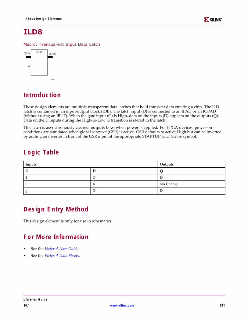
About Design Elements
ILD8
Macro: Transparent Input Data Latch
IntroductionThese design elements are multiple transparent data latches that hold transient data entering a chip. The ILDlatch is contained in an input/output block (IOB). The latch input (D) is connected to an IPAD or an IOPAD(without using an IBUF). When the gate input (G) is High, data on the inputs (D) appears on the outputs (Q).Data on the D inputs during the High-to-Low G transition is stored in the latch.
This latch is asynchronously cleared, outputs Low, when power is applied. For FPGA devices, power-onconditions are simulated when global set/reset (GSR) is active. GSR defaults to active-High but can be invertedby adding an inverter in front of the GSR input of the appropriate STARTUP_architecture symbol.
Logic TableInputs Outputs
G D Q
1 D D
0 X No Change
↓ D D
Design Entry MethodThis design element is only for use in schematics.
For More Information• See the Virtex-4 User Guide.
• See the Virtex-4 Data Sheets.
Libraries Guide
10.1 www.xilinx.com 331
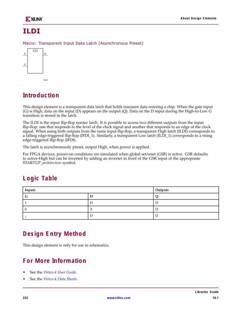
About Design Elements
ILDI
Macro: Transparent Input Data Latch (Asynchronous Preset)
IntroductionThis design element is a transparent data latch that holds transient data entering a chip. When the gate input(G) is High, data on the input (D) appears on the output (Q). Data on the D input during the High-to-Low Gtransition is stored in the latch.
The ILDI is the input flip-flop master latch. It is possible to access two different outputs from the inputflip-flop: one that responds to the level of the clock signal and another that responds to an edge of the clocksignal. When using both outputs from the same input flip-flop, a transparent High latch (ILDI) corresponds toa falling edge-triggered flip-flop (IFDI_1). Similarly, a transparent Low latch (ILDI_1) corresponds to a risingedge-triggered flip-flop (IFDI).
The latch is asynchronously preset, output High, when power is applied.
For FPGA devices, power-on conditions are simulated when global set/reset (GSR) is active. GSR defaultsto active-High but can be inverted by adding an inverter in front of the GSR input of the appropriateSTARTUP_architecture symbol.
Logic TableInputs Outputs
G D Q
1 D D
0 X D
↓ D D
Design Entry MethodThis design element is only for use in schematics.
For More Information• See the Virtex-4 User Guide.
• See the Virtex-4 Data Sheets.
Libraries Guide
332 www.xilinx.com 10.1
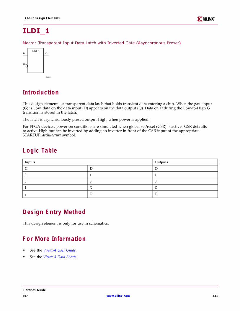
About Design Elements
ILDI_1
Macro: Transparent Input Data Latch with Inverted Gate (Asynchronous Preset)
IntroductionThis design element is a transparent data latch that holds transient data entering a chip. When the gate input(G) is Low, data on the data input (D) appears on the data output (Q). Data on D during the Low-to-High Gtransition is stored in the latch.
The latch is asynchronously preset, output High, when power is applied.
For FPGA devices, power-on conditions are simulated when global set/reset (GSR) is active. GSR defaultsto active-High but can be inverted by adding an inverter in front of the GSR input of the appropriateSTARTUP_architecture symbol.
Logic TableInputs Outputs
G D Q
0 1 1
0 0 0
1 X D
↑ D D
Design Entry MethodThis design element is only for use in schematics.
For More Information• See the Virtex-4 User Guide.
• See the Virtex-4 Data Sheets.
Libraries Guide
10.1 www.xilinx.com 333
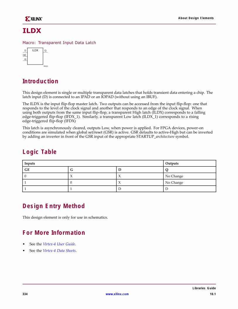
About Design Elements
ILDX
Macro: Transparent Input Data Latch
IntroductionThis design element is single or multiple transparent data latches that holds transient data entering a chip. Thelatch input (D) is connected to an IPAD or an IOPAD (without using an IBUF).
The ILDX is the input flip-flop master latch. Two outputs can be accessed from the input flip-flop: one thatresponds to the level of the clock signal and another that responds to an edge of the clock signal. Whenusing both outputs from the same input flip-flop, a transparent High latch (ILDX) corresponds to a fallingedge-triggered flip-flop (IFDX_1). Similarly, a transparent Low latch (ILDX_1) corresponds to a risingedge-triggered flip-flop (IFDX)
This latch is asynchronously cleared, outputs Low, when power is applied. For FPGA devices, power-onconditions are simulated when global set/reset (GSR) is active. GSR defaults to active-High but can be invertedby adding an inverter in front of the GSR input of the appropriate STARTUP_architecture symbol.
Logic TableInputs Outputs
GE G D Q
0 X X No Change
1 0 X No Change
1 1 D D
Design Entry MethodThis design element is only for use in schematics.
For More Information• See the Virtex-4 User Guide.
• See the Virtex-4 Data Sheets.
Libraries Guide
334 www.xilinx.com 10.1
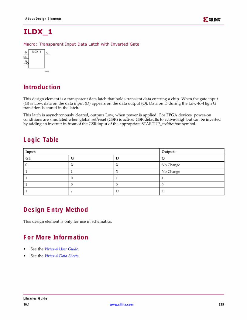
About Design Elements
ILDX_1
Macro: Transparent Input Data Latch with Inverted Gate
IntroductionThis design element is a transparent data latch that holds transient data entering a chip. When the gate input(G) is Low, data on the data input (D) appears on the data output (Q). Data on D during the Low-to-High Gtransition is stored in the latch.
This latch is asynchronously cleared, outputs Low, when power is applied. For FPGA devices, power-onconditions are simulated when global set/reset (GSR) is active. GSR defaults to active-High but can be invertedby adding an inverter in front of the GSR input of the appropriate STARTUP_architecture symbol.
Logic TableInputs Outputs
GE G D Q
0 X X No Change
1 1 X No Change
1 0 1 1
1 0 0 0
1 ↑ D D
Design Entry MethodThis design element is only for use in schematics.
For More Information• See the Virtex-4 User Guide.
• See the Virtex-4 Data Sheets.
Libraries Guide
10.1 www.xilinx.com 335

About Design Elements
ILDX16
Macro: Transparent Input Data Latch
IntroductionThis design element is single or multiple transparent data latches that holds transient data entering a chip. Thelatch input (D) is connected to an IPAD or an IOPAD (without using an IBUF).
The ILDX is the input flip-flop master latch. Two outputs can be accessed from the input flip-flop: one thatresponds to the level of the clock signal and another that responds to an edge of the clock signal. Whenusing both outputs from the same input flip-flop, a transparent High latch (ILDX) corresponds to a fallingedge-triggered flip-flop (IFDX_1). Similarly, a transparent Low latch (ILDX_1) corresponds to a risingedge-triggered flip-flop (IFDX)
This latch is asynchronously cleared, outputs Low, when power is applied. For FPGA devices, power-onconditions are simulated when global set/reset (GSR) is active. GSR defaults to active-High but can be invertedby adding an inverter in front of the GSR input of the appropriate STARTUP_architecture symbol.
Logic TableInputs Outputs
GE G D Q
0 X X No Change
1 0 X No Change
1 1 D D
Design Entry MethodThis design element is only for use in schematics.
For More Information• See the Virtex-4 User Guide.
• See the Virtex-4 Data Sheets.
Libraries Guide
336 www.xilinx.com 10.1
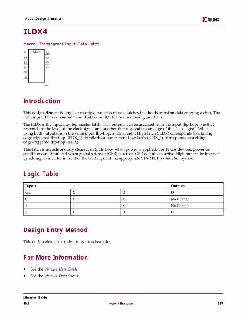
About Design Elements
ILDX4
Macro: Transparent Input Data Latch
IntroductionThis design element is single or multiple transparent data latches that holds transient data entering a chip. Thelatch input (D) is connected to an IPAD or an IOPAD (without using an IBUF).
The ILDX is the input flip-flop master latch. Two outputs can be accessed from the input flip-flop: one thatresponds to the level of the clock signal and another that responds to an edge of the clock signal. Whenusing both outputs from the same input flip-flop, a transparent High latch (ILDX) corresponds to a fallingedge-triggered flip-flop (IFDX_1). Similarly, a transparent Low latch (ILDX_1) corresponds to a risingedge-triggered flip-flop (IFDX)
This latch is asynchronously cleared, outputs Low, when power is applied. For FPGA devices, power-onconditions are simulated when global set/reset (GSR) is active. GSR defaults to active-High but can be invertedby adding an inverter in front of the GSR input of the appropriate STARTUP_architecture symbol.
Logic TableInputs Outputs
GE G D Q
0 X X No Change
1 0 X No Change
1 1 D D
Design Entry MethodThis design element is only for use in schematics.
For More Information• See the Virtex-4 User Guide.
• See the Virtex-4 Data Sheets.
Libraries Guide
10.1 www.xilinx.com 337
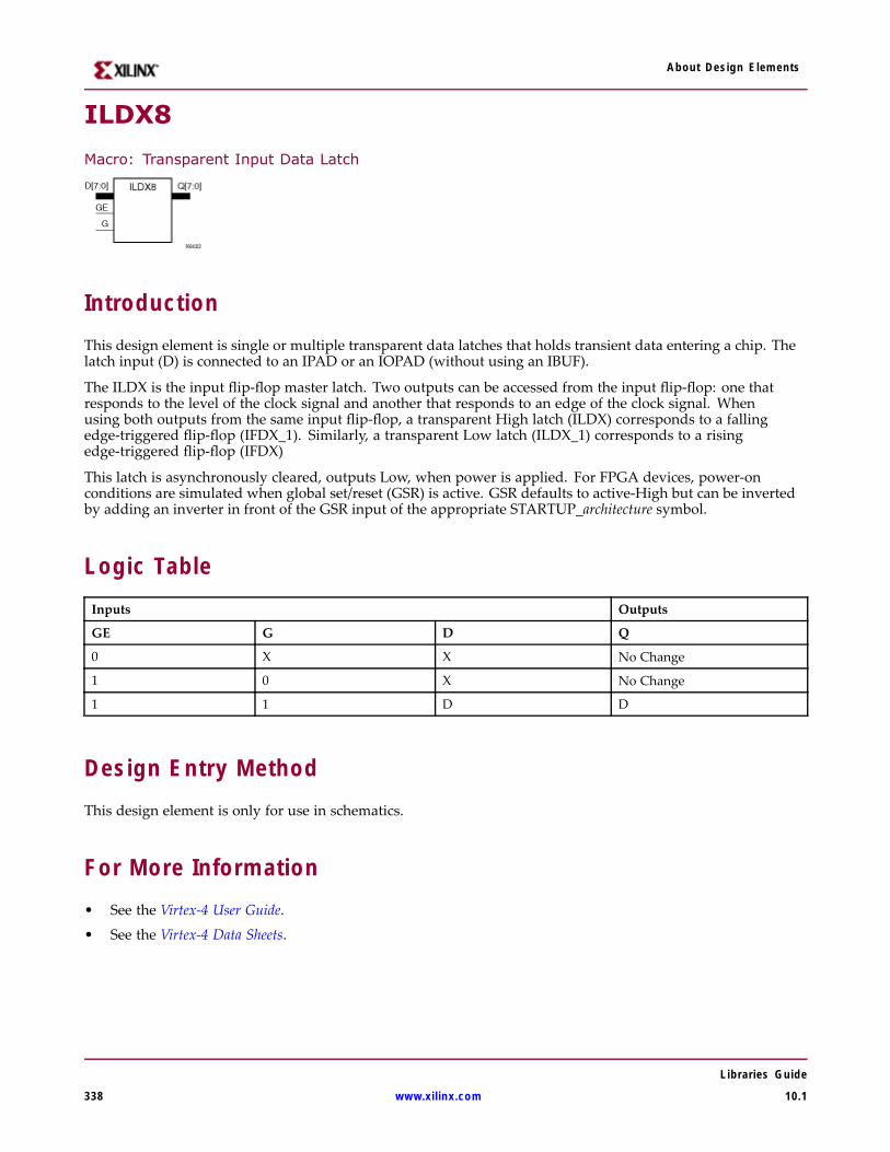
About Design Elements
ILDX8
Macro: Transparent Input Data Latch
IntroductionThis design element is single or multiple transparent data latches that holds transient data entering a chip. Thelatch input (D) is connected to an IPAD or an IOPAD (without using an IBUF).
The ILDX is the input flip-flop master latch. Two outputs can be accessed from the input flip-flop: one thatresponds to the level of the clock signal and another that responds to an edge of the clock signal. Whenusing both outputs from the same input flip-flop, a transparent High latch (ILDX) corresponds to a fallingedge-triggered flip-flop (IFDX_1). Similarly, a transparent Low latch (ILDX_1) corresponds to a risingedge-triggered flip-flop (IFDX)
This latch is asynchronously cleared, outputs Low, when power is applied. For FPGA devices, power-onconditions are simulated when global set/reset (GSR) is active. GSR defaults to active-High but can be invertedby adding an inverter in front of the GSR input of the appropriate STARTUP_architecture symbol.
Logic TableInputs Outputs
GE G D Q
0 X X No Change
1 0 X No Change
1 1 D D
Design Entry MethodThis design element is only for use in schematics.
For More Information• See the Virtex-4 User Guide.
• See the Virtex-4 Data Sheets.
Libraries Guide
338 www.xilinx.com 10.1
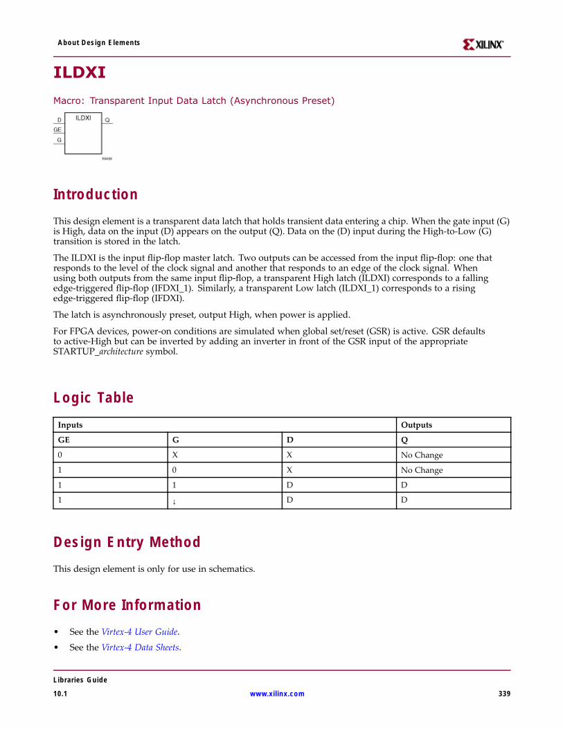
About Design Elements
ILDXI
Macro: Transparent Input Data Latch (Asynchronous Preset)
IntroductionThis design element is a transparent data latch that holds transient data entering a chip. When the gate input (G)is High, data on the input (D) appears on the output (Q). Data on the (D) input during the High-to-Low (G)transition is stored in the latch.
The ILDXI is the input flip-flop master latch. Two outputs can be accessed from the input flip-flop: one thatresponds to the level of the clock signal and another that responds to an edge of the clock signal. Whenusing both outputs from the same input flip-flop, a transparent High latch (ILDXI) corresponds to a fallingedge-triggered flip-flop (IFDXI_1). Similarly, a transparent Low latch (ILDXI_1) corresponds to a risingedge-triggered flip-flop (IFDXI).
The latch is asynchronously preset, output High, when power is applied.
For FPGA devices, power-on conditions are simulated when global set/reset (GSR) is active. GSR defaultsto active-High but can be inverted by adding an inverter in front of the GSR input of the appropriateSTARTUP_architecture symbol.
Logic TableInputs Outputs
GE G D Q
0 X X No Change
1 0 X No Change
1 1 D D
1 ↓ D D
Design Entry MethodThis design element is only for use in schematics.
For More Information• See the Virtex-4 User Guide.
• See the Virtex-4 Data Sheets.
Libraries Guide
10.1 www.xilinx.com 339
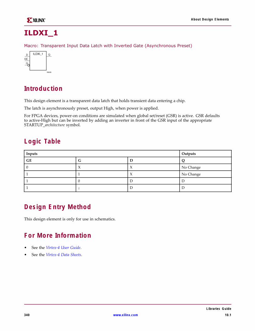
About Design Elements
ILDXI_1
Macro: Transparent Input Data Latch with Inverted Gate (Asynchronous Preset)
IntroductionThis design element is a transparent data latch that holds transient data entering a chip.
The latch is asynchronously preset, output High, when power is applied.
For FPGA devices, power-on conditions are simulated when global set/reset (GSR) is active. GSR defaultsto active-High but can be inverted by adding an inverter in front of the GSR input of the appropriateSTARTUP_architecture symbol.
Logic TableInputs Outputs
GE G D Q
0 X X No Change
1 1 X No Change
1 0 D D
1 ↑ D D
Design Entry MethodThis design element is only for use in schematics.
For More Information• See the Virtex-4 User Guide.
• See the Virtex-4 Data Sheets.
Libraries Guide
340 www.xilinx.com 10.1
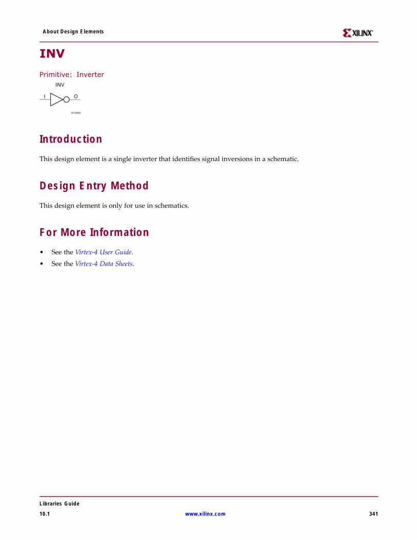
About Design Elements
INV
Primitive: Inverter
IntroductionThis design element is a single inverter that identifies signal inversions in a schematic.
Design Entry MethodThis design element is only for use in schematics.
For More Information• See the Virtex-4 User Guide.
• See the Virtex-4 Data Sheets.
Libraries Guide
10.1 www.xilinx.com 341
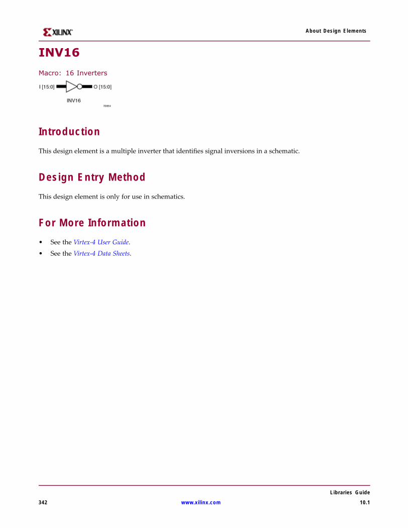
About Design Elements
INV16
Macro: 16 Inverters
IntroductionThis design element is a multiple inverter that identifies signal inversions in a schematic.
Design Entry MethodThis design element is only for use in schematics.
For More Information• See the Virtex-4 User Guide.
• See the Virtex-4 Data Sheets.
Libraries Guide
342 www.xilinx.com 10.1
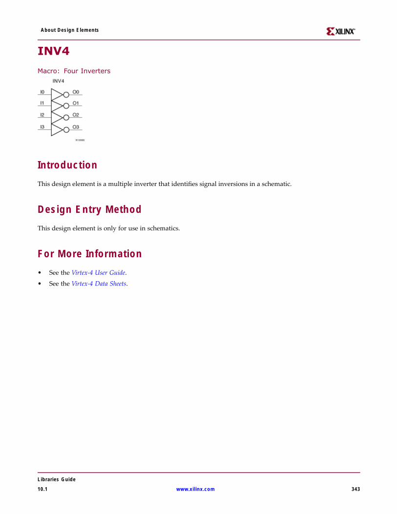
About Design Elements
INV4
Macro: Four Inverters
IntroductionThis design element is a multiple inverter that identifies signal inversions in a schematic.
Design Entry MethodThis design element is only for use in schematics.
For More Information• See the Virtex-4 User Guide.
• See the Virtex-4 Data Sheets.
Libraries Guide
10.1 www.xilinx.com 343
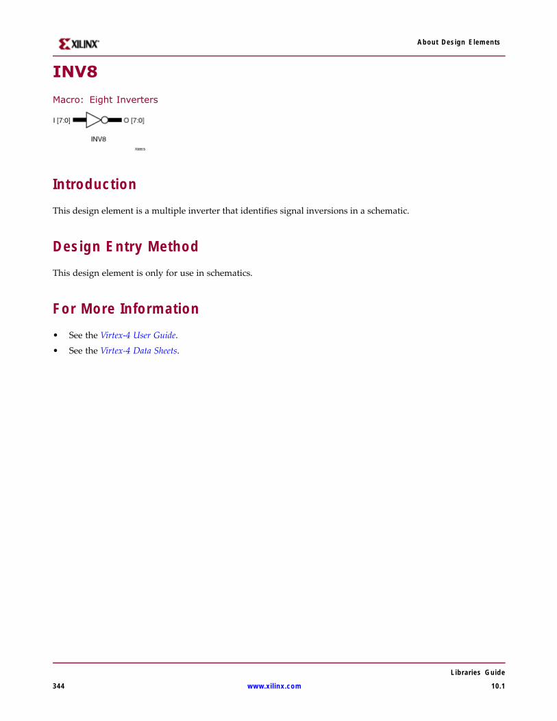
About Design Elements
INV8
Macro: Eight Inverters
IntroductionThis design element is a multiple inverter that identifies signal inversions in a schematic.
Design Entry MethodThis design element is only for use in schematics.
For More Information• See the Virtex-4 User Guide.
• See the Virtex-4 Data Sheets.
Libraries Guide
344 www.xilinx.com 10.1
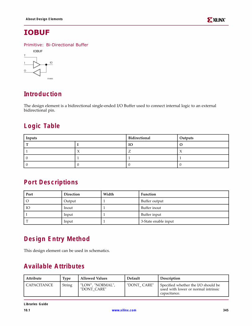
About Design Elements
IOBUF
Primitive: Bi-Directional Buffer
IntroductionThe design element is a bidirectional single-ended I/O Buffer used to connect internal logic to an externalbidirectional pin.
Logic TableInputs Bidirectional Outputs
T I IO O
1 X Z X
0 1 1 1
0 0 0 0
Port DescriptionsPort Direction Width Function
O Output 1 Buffer output
IO Inout 1 Buffer inout
I Input 1 Buffer input
T Input 1 3-State enable input
Design Entry MethodThis design element can be used in schematics.
Available AttributesAttribute Type Allowed Values Default Description
CAPACITANCE String "LOW", "NORMAL","DONT_CARE"
"DONT_ CARE" Specified whether the I/O should beused with lower or normal intrinsiccapacitance.
Libraries Guide
10.1 www.xilinx.com 345
About Design Elements
Attribute Type Allowed Values Default Description
DRIVE Integer 2, 4, 6, 8, 12, 16, 24 12 Selects output drive strength (mA) forthe SelectIO buffers that use the LVTTL,LVCMOS12, LVCMOS15, LVCMOS18,LVCMOS25, or LVCMOS33 interface I/Ostandard.
IOSTANDARD String See Data Sheet "DEFAULT" Assigns an I/O standard to the element.
SLEW String "SLOW", "FAST" "SLOW" Sets the output rise and fall time. See theData Sheet for recommendations of thebest setting for this attribute.
For More Information• See the Virtex-4 User Guide.
• See the Virtex-4 Data Sheets.
Libraries Guide
346 www.xilinx.com 10.1
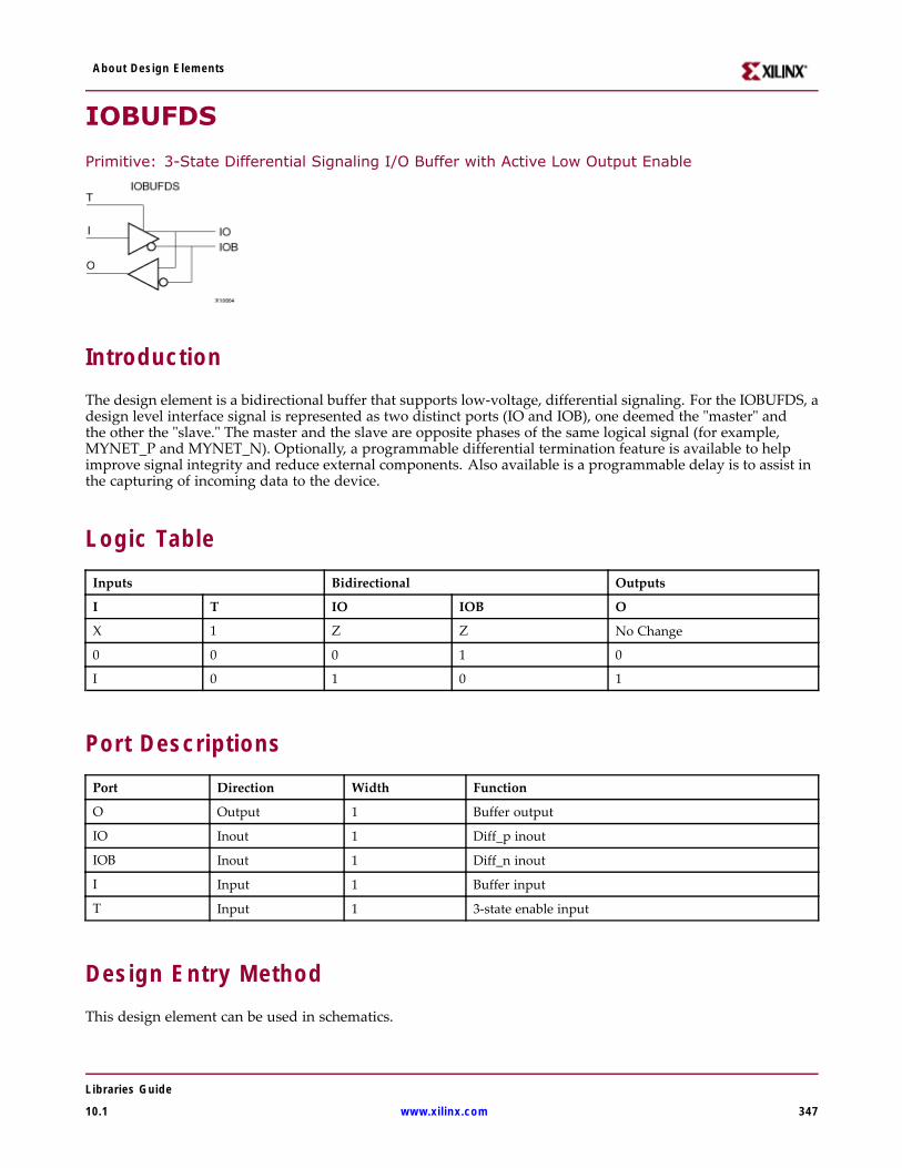
About Design Elements
IOBUFDS
Primitive: 3-State Differential Signaling I/O Buffer with Active Low Output Enable
IntroductionThe design element is a bidirectional buffer that supports low-voltage, differential signaling. For the IOBUFDS, adesign level interface signal is represented as two distinct ports (IO and IOB), one deemed the "master" andthe other the "slave." The master and the slave are opposite phases of the same logical signal (for example,MYNET_P and MYNET_N). Optionally, a programmable differential termination feature is available to helpimprove signal integrity and reduce external components. Also available is a programmable delay is to assist inthe capturing of incoming data to the device.
Logic TableInputs Bidirectional Outputs
I T IO IOB O
X 1 Z Z No Change
0 0 0 1 0
I 0 1 0 1
Port DescriptionsPort Direction Width Function
O Output 1 Buffer output
IO Inout 1 Diff_p inout
IOB Inout 1 Diff_n inout
I Input 1 Buffer input
T Input 1 3-state enable input
Design Entry MethodThis design element can be used in schematics.
Libraries Guide
10.1 www.xilinx.com 347

About Design Elements
Available AttributesAttribute Type Allowed Values Default Description
CAPACITANCE String "LOW","NORMAL","DONT_CARE"
"DONT_ CARE" Specified whether the I/O should beused with lower or normal intrinsiccapacitance.
IOSTANDARD String See Data Sheet "DEFAULT" Assigns an I/O standard to the element.
For More Information• See the Virtex-4 User Guide.
• See the Virtex-4 Data Sheets.
Libraries Guide
348 www.xilinx.com 10.1
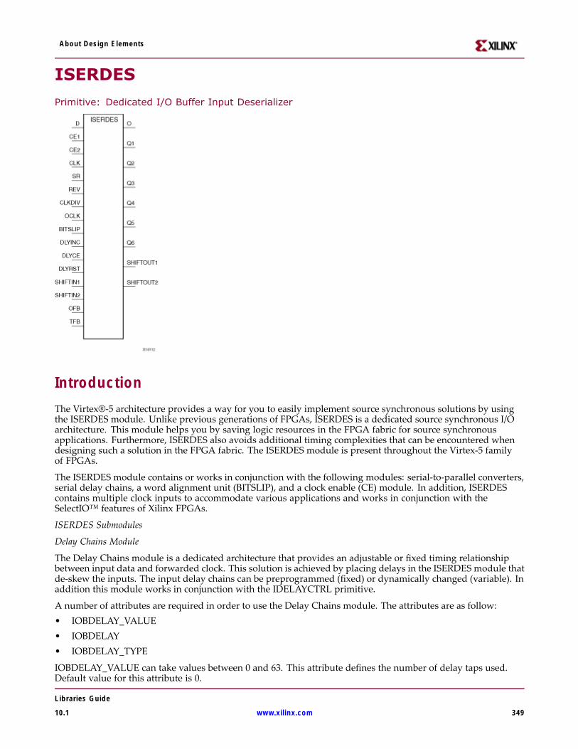
About Design Elements
ISERDES
Primitive: Dedicated I/O Buffer Input Deserializer
IntroductionThe Virtex®-5 architecture provides a way for you to easily implement source synchronous solutions by usingthe ISERDES module. Unlike previous generations of FPGAs, ISERDES is a dedicated source synchronous I/Oarchitecture. This module helps you by saving logic resources in the FPGA fabric for source synchronousapplications. Furthermore, ISERDES also avoids additional timing complexities that can be encountered whendesigning such a solution in the FPGA fabric. The ISERDES module is present throughout the Virtex-5 familyof FPGAs.
The ISERDES module contains or works in conjunction with the following modules: serial-to-parallel converters,serial delay chains, a word alignment unit (BITSLIP), and a clock enable (CE) module. In addition, ISERDEScontains multiple clock inputs to accommodate various applications and works in conjunction with theSelectIO™ features of Xilinx FPGAs.
ISERDES Submodules
Delay Chains Module
The Delay Chains module is a dedicated architecture that provides an adjustable or fixed timing relationshipbetween input data and forwarded clock. This solution is achieved by placing delays in the ISERDES module thatde-skew the inputs. The input delay chains can be preprogrammed (fixed) or dynamically changed (variable). Inaddition this module works in conjunction with the IDELAYCTRL primitive.
A number of attributes are required in order to use the Delay Chains module. The attributes are as follow:• IOBDELAY_VALUE• IOBDELAY• IOBDELAY_TYPE
IOBDELAY_VALUE can take values between 0 and 63. This attribute defines the number of delay taps used.Default value for this attribute is 0.
Libraries Guide
10.1 www.xilinx.com 349
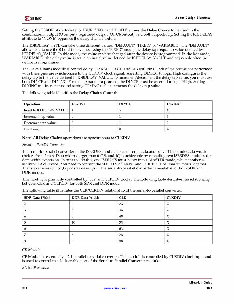
About Design Elements
Setting the IOBDELAY attribute to "IBUF," "IFD," and "BOTH" allows the Delay Chains to be used in thecombinatorial output (O output), registered output (Q1-Q6 output), and both respectively. Setting the IOBDELAYattribute to "NONE" bypasses the delay chains module.
The IOBDELAY_TYPE can take three different values: "DEFAULT," "FIXED," or "VARIABLE." The "DEFAULT"allows you to use the 0 hold time value. Using the "FIXED" mode, the delay taps equal to value defined byIOBDELAY_VALUE. In this mode, the value can’t be changed after the device is programmed. In the last mode,"VARIABLE," the delay value is set to an initial value defined by IOBDELAY_VALUE and adjustable after thedevice is programmed.
The Delay Chains module is controlled by DLYRST, DLYCE, and DLYINC pins. Each of the operations performedwith these pins are synchronous to the CLKDIV clock signal. Asserting DLYRST to logic High configures thedelay tap to the value defined in IOBDELAY_VALUE. To increment/decrement the delay tap value, you must useboth DLYCE and DLYINC. For this operation to proceed, the DLYCE must be asserted to logic High. SettingDLYINC to 1 increments and setting DLYINC to 0 decrements the delay tap value.
The following table identifies the Delay Chains Controls:
Operation DLYRST DLYCE DLYINC
Reset to IOBDELAY_VALUE 1 X X
Increment tap value 0 1 1
Decrement tap value 0 1 0
No change 0 0 X
Note All Delay Chains operations are synchronous to CLKDIV.
Serial-to-Parallel Converter
The serial-to-parallel converter in the ISERDES module takes in serial data and convert them into data widthchoices from 2 to 6. Data widths larger than 6 (7,8, and 10) is achievable by cascading two ISERDES modules fordata width expansion. In order to do this, one ISERDES must be set into a MASTER mode, while another isset into SLAVE mode. You need to connect the SHIFTIN of "slave" and SHIFTOUT of "master" ports together.The "slave" uses Q3 to Q6 ports as its output. The serial-to-parallel converter is available for both SDR andDDR modes.
This module is primarily controlled by CLK and CLKDIV clocks. The following table describes the relationshipbetween CLK and CLKDIV for both SDR and DDR mode.
The following table illustrates the CLK/CLKDIV relationship of the serial-to-parallel converter:
SDR Data Width DDR Data Width CLK CLKDIV
2 4 2X X
3 6 3X X
4 8 4X X
5 10 5X X
6 - 6X X
7 - 7X X
8 - 8X X
CE Module
CE Module is essentially a 2:1 parallel-to-serial converter. This module is controlled by CLKDIV clock input andis used to control the clock enable port of the Serial-to-Parallel Converter module.
BITSLIP Module
Libraries Guide
350 www.xilinx.com 10.1
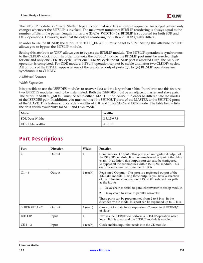
About Design Elements
The BITSLIP module is a "Barrel Shifter" type function that reorders an output sequence. An output pattern onlychanges whenever the BITSLIP is invoked. The maximum number of BITSLIP reordering is always equal to thenumber of bits in the pattern length minus one (DATA_WIDTH – 1). BITSLIP is supported for both SDR andDDR operations. However, note that the output reordering for SDR and DDR greatly differs.
In order to use the BITSLIP, the attribute "BITSLIP_ENABLE" must be set to "ON." Setting this attribute to "OFF"allows you to bypass the BITSLIP module.
Setting this attribute to "OFF" allows you to bypass the BITSLIP module. The BITSLIP operation is synchronousto the CLKDIV clock input. In order to invoke the BITSLIP module, the BITSLIP port must be asserted Highfor one and only one CLKDIV cycle. After one CLKDIV cycle the BITSLIP port is asserted High, the BITSLIPoperation is completed. For DDR mode, a BITSLIP operation can not be stable until after two CLKDIV cycles.All outputs of the BITSLIP appear in one of the registered output ports (Q1 to Q6) BITSLIP operations aresynchronous to CLKDIV.
Additional Features
Width Expansion
It is possible to use the ISERDES modules to recover data widths larger than 6 bits. In order to use this feature,two ISERDES modules need to be instantiated. Both the ISERDES must be an adjacent master and slave pair.The attribute SERDES_MODE must be set to either "MASTER" or "SLAVE" in order to differentiate the modesof the ISERDES pair. In addition, you must connect the SHIFOUT ports of the MASTER to the SHIFTIN portsof the SLAVE. This feature supports data widths of 7, 8, and 10 for SDR and DDR mode. The table below liststhe data width availability for SDR and DDR mode.
Mode Widths
SDR Data Widths 2,3,4,5,6,7,8
DDR Data Widths 4,6,8,10
Port DescriptionsPort Direction Width Function
O Output 1 Combinatorial Output - This port is an unregistered output ofthe ISERDES module. It is the unregistered output of the delaychain. In addition, this output port can also be configuredto bypass all the submodules within ISERDES module. Thisoutput can be used to drive the BUFIOs.
Q1 – 6 Output 1 (each) Registered Outputs - This port is a registered output of theISERDES module. Using these outputs, you have a selectionof the following combination of ISERDES submodules pathas the inputs:
1. Delay chain to serial-to-parallel converter to bitslip module.
2. Delay chain to serial-to-parallel converter.
These ports can be programmed from 2 to 6 bits. In theextended width mode, this port can be expanded up to 10 bits.
SHIFTOUT 1 – 2 Output 1 (each) Carry out for data input expansion. Connect to SHIFTIN1/2of slave.
BITSLIP Input 1 Invokes the ISERDES to perform a BITSLIP operation whenlogic High is given and the BITSLIP module is enabled.
CE 1 – 2 Input 1 (each) Clock enables input that feeds into the CE module.
Libraries Guide
10.1 www.xilinx.com 351
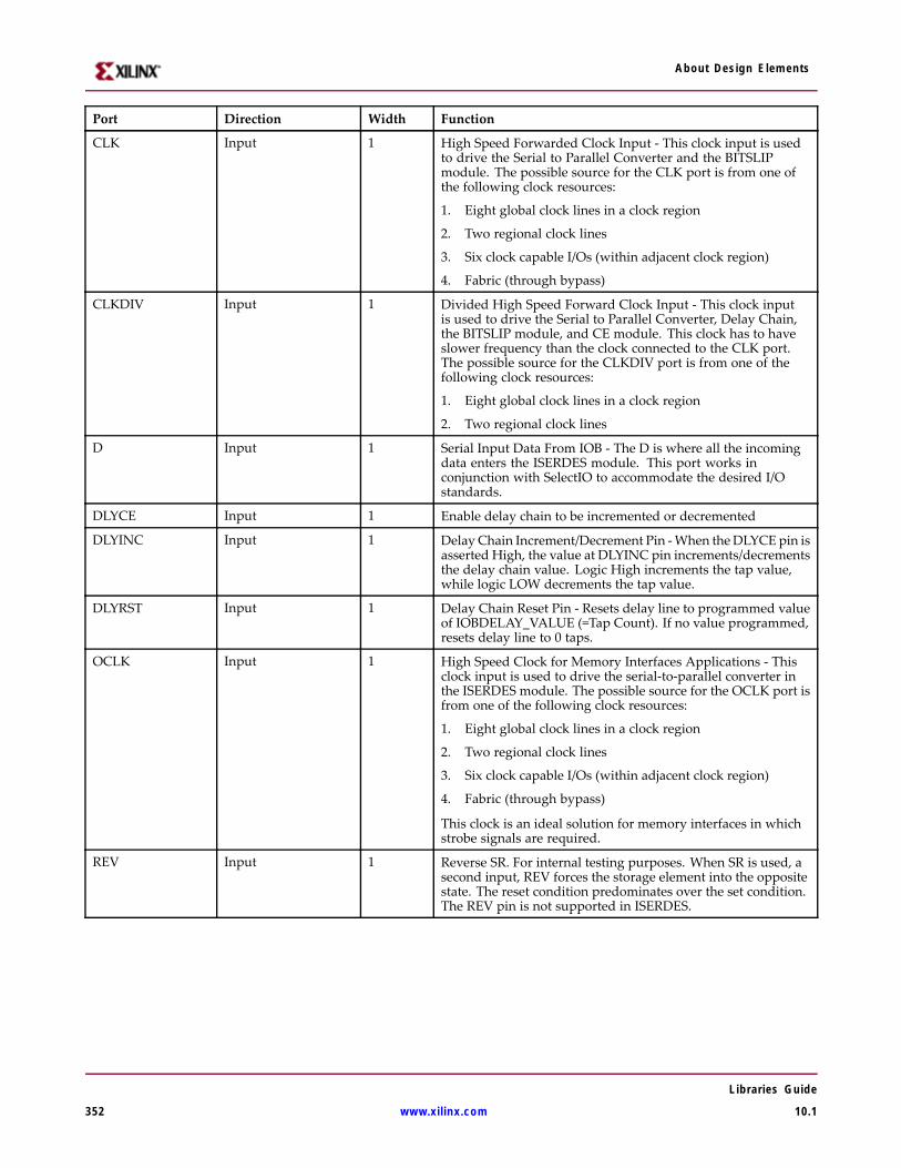
About Design Elements
Port Direction Width Function
CLK Input 1 High Speed Forwarded Clock Input - This clock input is usedto drive the Serial to Parallel Converter and the BITSLIPmodule. The possible source for the CLK port is from one ofthe following clock resources:
1. Eight global clock lines in a clock region
2. Two regional clock lines
3. Six clock capable I/Os (within adjacent clock region)
4. Fabric (through bypass)
CLKDIV Input 1 Divided High Speed Forward Clock Input - This clock inputis used to drive the Serial to Parallel Converter, Delay Chain,the BITSLIP module, and CE module. This clock has to haveslower frequency than the clock connected to the CLK port.The possible source for the CLKDIV port is from one of thefollowing clock resources:
1. Eight global clock lines in a clock region
2. Two regional clock lines
D Input 1 Serial Input Data From IOB - The D is where all the incomingdata enters the ISERDES module. This port works inconjunction with SelectIO to accommodate the desired I/Ostandards.
DLYCE Input 1 Enable delay chain to be incremented or decremented
DLYINC Input 1 Delay Chain Increment/Decrement Pin -When theDLYCE pin isasserted High, the value at DLYINC pin increments/decrementsthe delay chain value. Logic High increments the tap value,while logic LOW decrements the tap value.
DLYRST Input 1 Delay Chain Reset Pin - Resets delay line to programmed valueof IOBDELAY_VALUE (=Tap Count). If no value programmed,resets delay line to 0 taps.
OCLK Input 1 High Speed Clock for Memory Interfaces Applications - Thisclock input is used to drive the serial-to-parallel converter inthe ISERDES module. The possible source for the OCLK port isfrom one of the following clock resources:
1. Eight global clock lines in a clock region
2. Two regional clock lines
3. Six clock capable I/Os (within adjacent clock region)
4. Fabric (through bypass)
This clock is an ideal solution for memory interfaces in whichstrobe signals are required.
REV Input 1 Reverse SR. For internal testing purposes. When SR is used, asecond input, REV forces the storage element into the oppositestate. The reset condition predominates over the set condition.The REV pin is not supported in ISERDES.
Libraries Guide
352 www.xilinx.com 10.1
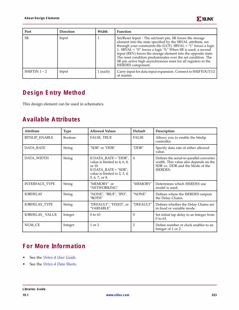
About Design Elements
Port Direction Width Function
SR Input 1 Set/Reset Input - The set/reset pin, SR forces the storageelement into the state specified by the SRVAL attribute, setthrough your constraints file (UCF). SRVAL = “1” forces a logic1. SRVAL = “0” forces a logic "0." When SR is used, a secondinput (REV) forces the storage element into the opposite state.The reset condition predominates over the set condition. TheSR pin active high asynchronous reset for all registers in theISERDES component.
SHIFTIN 1 – 2 Input 1 (each) Carry input for data input expansion. Connect to SHIFTOUT1/2of master.
Design Entry MethodThis design element can be used in schematics.
Available AttributesAttribute Type Allowed Values Default Description
BITSLIP_ENABLE Boolean FALSE, TRUE FALSE Allows you to enable the bitslipcontroller.
DATA_RATE String "SDR" or "DDR" "DDR” Specify data rate of either allowedvalue.
DATA_WIDTH String If DATA_RATE = "DDR",value is limited to 4, 6, 8,or 10.If DATA_RATE = "SDR",value is limited to 2, 3, 4,5, 6, 7, or 8.
4 Defines the serial-to-parallel converterwidth. This value also depends on theSDR vs. DDR and the Mode of theISERDES.
INTERFACE_TYPE String "MEMORY" or"NETWORKING"
"MEMORY" Determines which ISERDES usemodel is used.
IOBDELAY String "NONE", "IBUF", "IFD","BOTH"
"NONE" Defines where the ISERDES outputsthe Delay Chains.
IOBDELAY_TYPE String "DEFAULT", "FIXED", or"VARIABLE"
"DEFAULT" Defines whether the Delay Chains arein fixed or variable mode.
IOBDELAY_ VALUE Integer 0 to 63 0 Set initial tap delay to an Integer from0 to 63.
NUM_CE Integer 1 or 2 2 Define number or clock enables to anInteger of 1 or 2.
For More Information• See the Virtex-4 User Guide.
• See the Virtex-4 Data Sheets.
Libraries Guide
10.1 www.xilinx.com 353
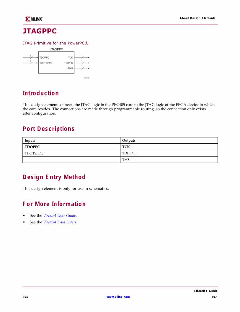
About Design Elements
JTAGPPC
JTAG Primitive for the PowerPC®
IntroductionThis design element connects the JTAG logic in the PPC405 core to the JTAG logic of the FPGA device in whichthe core resides. The connections are made through programmable routing, so the connection only existsafter configuration.
Port DescriptionsInputs Outputs
TDOPPC TCK
TDOTSPPC TDIPPC
TMS
Design Entry MethodThis design element is only for use in schematics.
For More Information• See the Virtex-4 User Guide.
• See the Virtex-4 Data Sheets.
Libraries Guide
354 www.xilinx.com 10.1

About Design Elements
KEEPER
Primitive: KEEPER Symbol
IntroductionThe design element is a weak keeper element that retains the value of the net connected to its bidirectional O pin.For example, if a logic 1 is being driven onto the net, KEEPER drives a weak/resistive 1 onto the net. If the netdriver is then 3-stated, KEEPER continues to drive a weak/resistive 1 onto the net.
Port DescriptionsName Direction Width Function
O Output 1-Bit Keeper output
Design Entry MethodThis design element can be used in schematics.
This element can be connected to a net in the following locations on a top-level schematic file:
• A net connected to an input IO Marker
• A net connected to both an output IO Marker and 3-statable IO element, such as an OBUFT.
For More Information• See the Virtex-4 User Guide.
• See the Virtex-4 Data Sheets.
Libraries Guide
10.1 www.xilinx.com 355
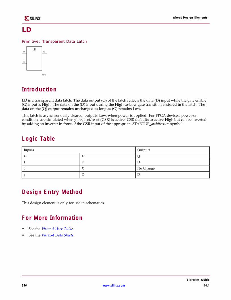
About Design Elements
LD
Primitive: Transparent Data Latch
IntroductionLD is a transparent data latch. The data output (Q) of the latch reflects the data (D) input while the gate enable(G) input is High. The data on the (D) input during the High-to-Low gate transition is stored in the latch. Thedata on the (Q) output remains unchanged as long as (G) remains Low.
This latch is asynchronously cleared, outputs Low, when power is applied. For FPGA devices, power-onconditions are simulated when global set/reset (GSR) is active. GSR defaults to active-High but can be invertedby adding an inverter in front of the GSR input of the appropriate STARTUP_architecture symbol.
Logic TableInputs Outputs
G D Q
1 D D
0 X No Change
↓ D D
Design Entry MethodThis design element is only for use in schematics.
For More Information• See the Virtex-4 User Guide.
• See the Virtex-4 Data Sheets.
Libraries Guide
356 www.xilinx.com 10.1
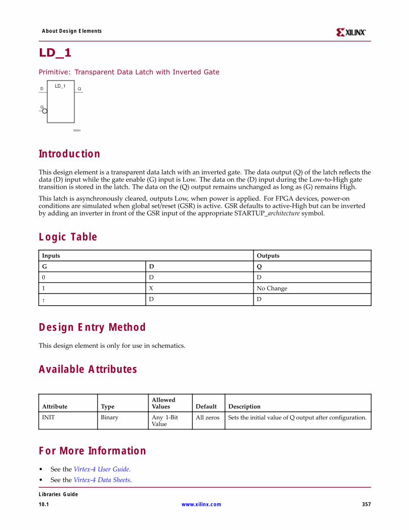
About Design Elements
LD_1
Primitive: Transparent Data Latch with Inverted Gate
IntroductionThis design element is a transparent data latch with an inverted gate. The data output (Q) of the latch reflects thedata (D) input while the gate enable (G) input is Low. The data on the (D) input during the Low-to-High gatetransition is stored in the latch. The data on the (Q) output remains unchanged as long as (G) remains High.
This latch is asynchronously cleared, outputs Low, when power is applied. For FPGA devices, power-onconditions are simulated when global set/reset (GSR) is active. GSR defaults to active-High but can be invertedby adding an inverter in front of the GSR input of the appropriate STARTUP_architecture symbol.
Logic TableInputs Outputs
G D Q
0 D D
1 X No Change
↑ D D
Design Entry MethodThis design element is only for use in schematics.
Available Attributes
Attribute TypeAllowedValues Default Description
INIT Binary Any 1-BitValue
All zeros Sets the initial value of Q output after configuration.
For More Information• See the Virtex-4 User Guide.• See the Virtex-4 Data Sheets.
Libraries Guide
10.1 www.xilinx.com 357
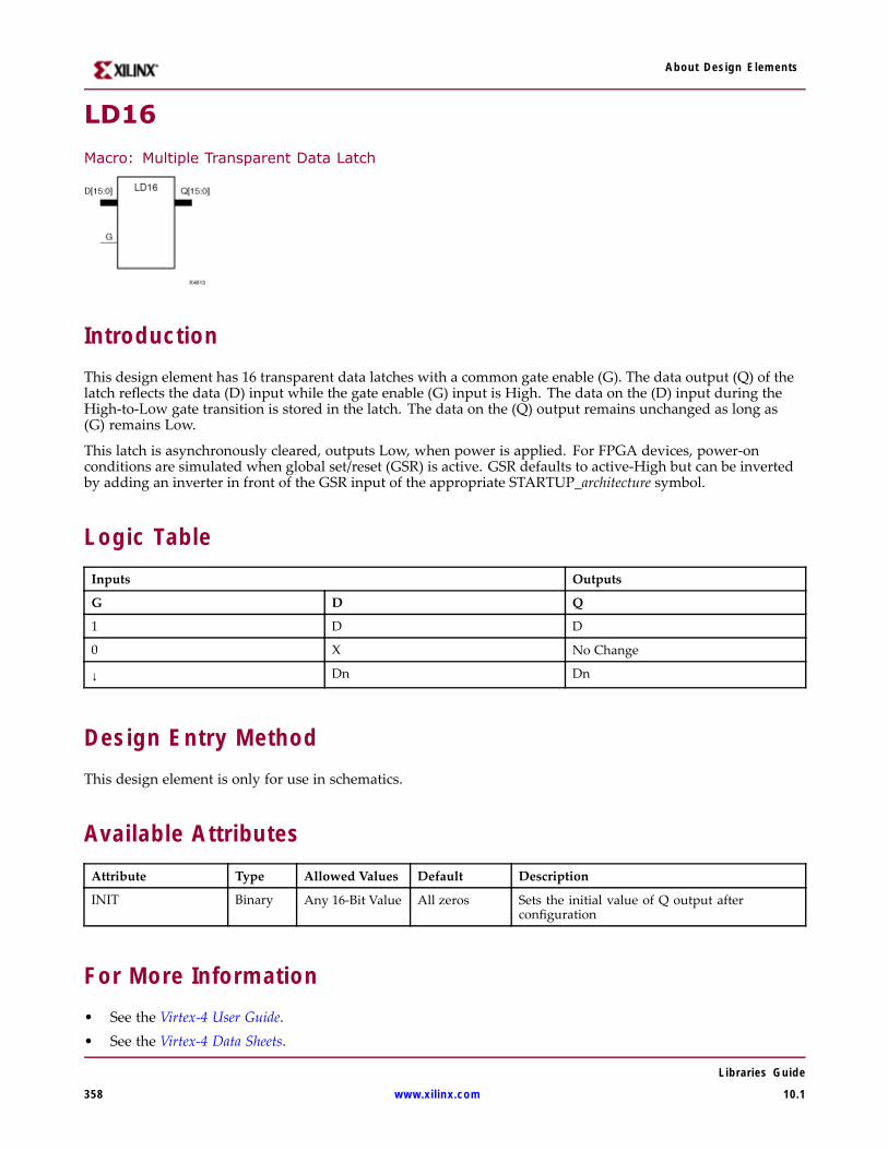
About Design Elements
LD16
Macro: Multiple Transparent Data Latch
IntroductionThis design element has 16 transparent data latches with a common gate enable (G). The data output (Q) of thelatch reflects the data (D) input while the gate enable (G) input is High. The data on the (D) input during theHigh-to-Low gate transition is stored in the latch. The data on the (Q) output remains unchanged as long as(G) remains Low.
This latch is asynchronously cleared, outputs Low, when power is applied. For FPGA devices, power-onconditions are simulated when global set/reset (GSR) is active. GSR defaults to active-High but can be invertedby adding an inverter in front of the GSR input of the appropriate STARTUP_architecture symbol.
Logic TableInputs Outputs
G D Q
1 D D
0 X No Change
↓ Dn Dn
Design Entry MethodThis design element is only for use in schematics.
Available AttributesAttribute Type Allowed Values Default Description
INIT Binary Any 16-Bit Value All zeros Sets the initial value of Q output afterconfiguration
For More Information• See the Virtex-4 User Guide.• See the Virtex-4 Data Sheets.
Libraries Guide
358 www.xilinx.com 10.1
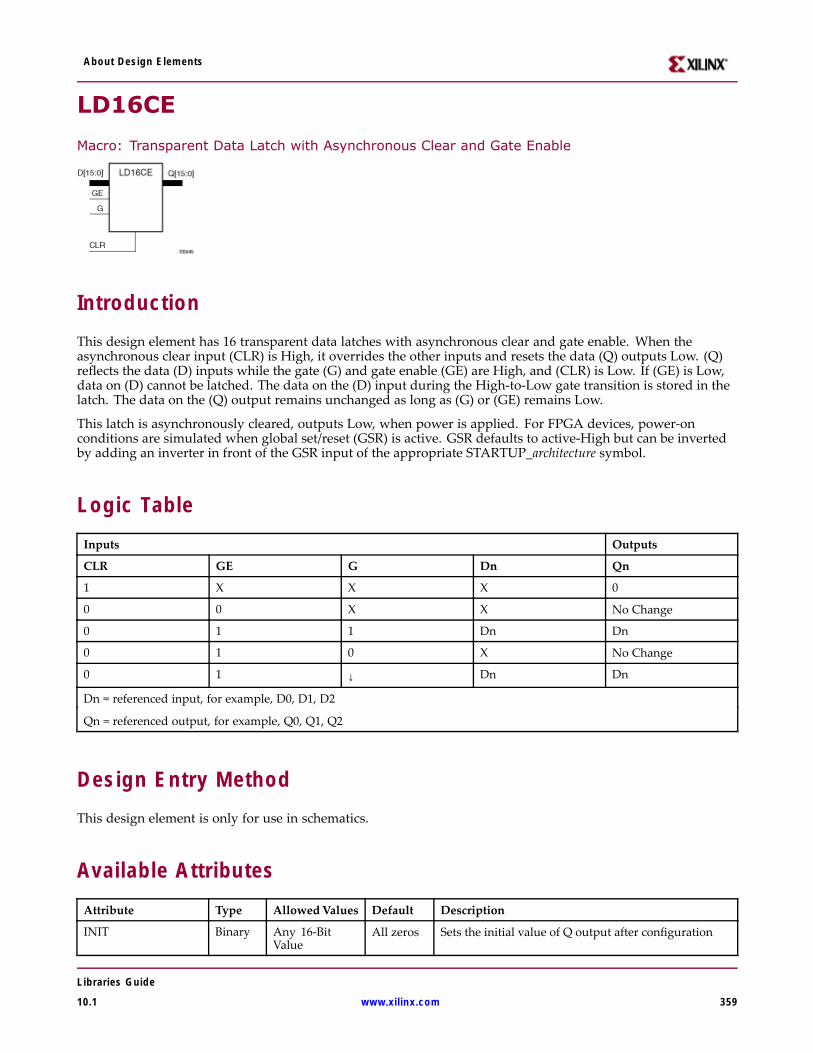
About Design Elements
LD16CE
Macro: Transparent Data Latch with Asynchronous Clear and Gate Enable
IntroductionThis design element has 16 transparent data latches with asynchronous clear and gate enable. When theasynchronous clear input (CLR) is High, it overrides the other inputs and resets the data (Q) outputs Low. (Q)reflects the data (D) inputs while the gate (G) and gate enable (GE) are High, and (CLR) is Low. If (GE) is Low,data on (D) cannot be latched. The data on the (D) input during the High-to-Low gate transition is stored in thelatch. The data on the (Q) output remains unchanged as long as (G) or (GE) remains Low.
This latch is asynchronously cleared, outputs Low, when power is applied. For FPGA devices, power-onconditions are simulated when global set/reset (GSR) is active. GSR defaults to active-High but can be invertedby adding an inverter in front of the GSR input of the appropriate STARTUP_architecture symbol.
Logic TableInputs Outputs
CLR GE G Dn Qn
1 X X X 0
0 0 X X No Change
0 1 1 Dn Dn
0 1 0 X No Change
0 1 ↓ Dn Dn
Dn = referenced input, for example, D0, D1, D2
Qn = referenced output, for example, Q0, Q1, Q2
Design Entry MethodThis design element is only for use in schematics.
Available AttributesAttribute Type AllowedValues Default Description
INIT Binary Any 16-BitValue
All zeros Sets the initial value of Q output after configuration
Libraries Guide
10.1 www.xilinx.com 359

About Design Elements
For More Information• See the Virtex-4 User Guide.
• See the Virtex-4 Data Sheets.
Libraries Guide
360 www.xilinx.com 10.1
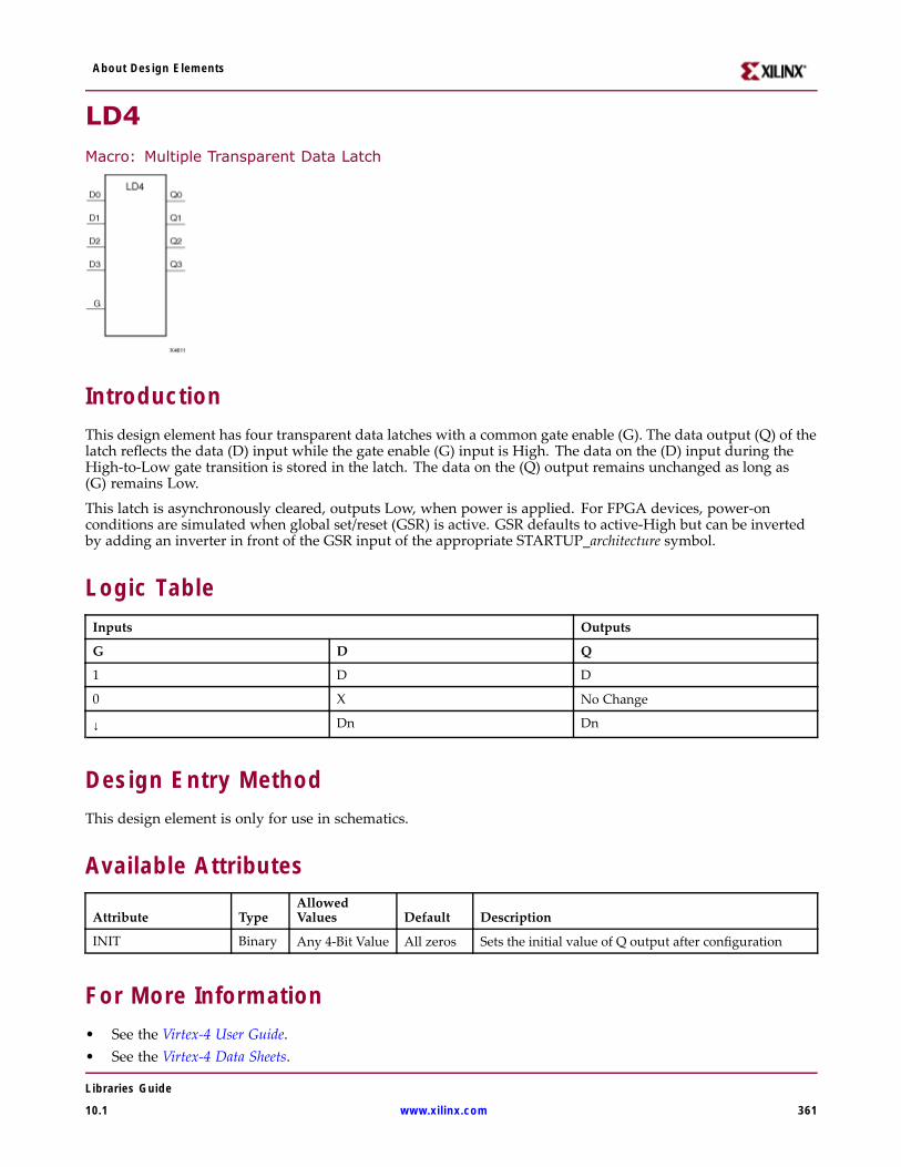
About Design Elements
LD4Macro: Multiple Transparent Data Latch
IntroductionThis design element has four transparent data latches with a common gate enable (G). The data output (Q) of thelatch reflects the data (D) input while the gate enable (G) input is High. The data on the (D) input during theHigh-to-Low gate transition is stored in the latch. The data on the (Q) output remains unchanged as long as(G) remains Low.
This latch is asynchronously cleared, outputs Low, when power is applied. For FPGA devices, power-onconditions are simulated when global set/reset (GSR) is active. GSR defaults to active-High but can be invertedby adding an inverter in front of the GSR input of the appropriate STARTUP_architecture symbol.
Logic TableInputs Outputs
G D Q
1 D D
0 X No Change
↓ Dn Dn
Design Entry MethodThis design element is only for use in schematics.
Available Attributes
Attribute TypeAllowedValues Default Description
INIT Binary Any 4-Bit Value All zeros Sets the initial value of Q output after configuration
For More Information• See the Virtex-4 User Guide.• See the Virtex-4 Data Sheets.
Libraries Guide
10.1 www.xilinx.com 361
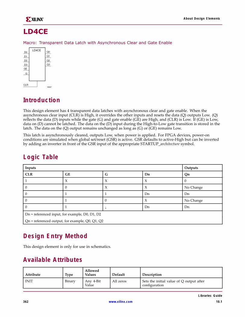
About Design Elements
LD4CEMacro: Transparent Data Latch with Asynchronous Clear and Gate Enable
IntroductionThis design element has 4 transparent data latches with asynchronous clear and gate enable. When theasynchronous clear input (CLR) is High, it overrides the other inputs and resets the data (Q) outputs Low. (Q)reflects the data (D) inputs while the gate (G) and gate enable (GE) are High, and (CLR) is Low. If (GE) is Low,data on (D) cannot be latched. The data on the (D) input during the High-to-Low gate transition is stored in thelatch. The data on the (Q) output remains unchanged as long as (G) or (GE) remains Low.
This latch is asynchronously cleared, outputs Low, when power is applied. For FPGA devices, power-onconditions are simulated when global set/reset (GSR) is active. GSR defaults to active-High but can be invertedby adding an inverter in front of the GSR input of the appropriate STARTUP_architecture symbol.
Logic TableInputs Outputs
CLR GE G Dn Qn
1 X X X 0
0 0 X X No Change
0 1 1 Dn Dn
0 1 0 X No Change
0 1 ↓ Dn Dn
Dn = referenced input, for example, D0, D1, D2
Qn = referenced output, for example, Q0, Q1, Q2
Design Entry MethodThis design element is only for use in schematics.
Available Attributes
Attribute TypeAllowedValues Default Description
INIT Binary Any 4-BitValue
All zeros Sets the initial value of Q output afterconfiguration
Libraries Guide
362 www.xilinx.com 10.1

About Design Elements
For More Information• See the Virtex-4 User Guide.
• See the Virtex-4 Data Sheets.
Libraries Guide
10.1 www.xilinx.com 363
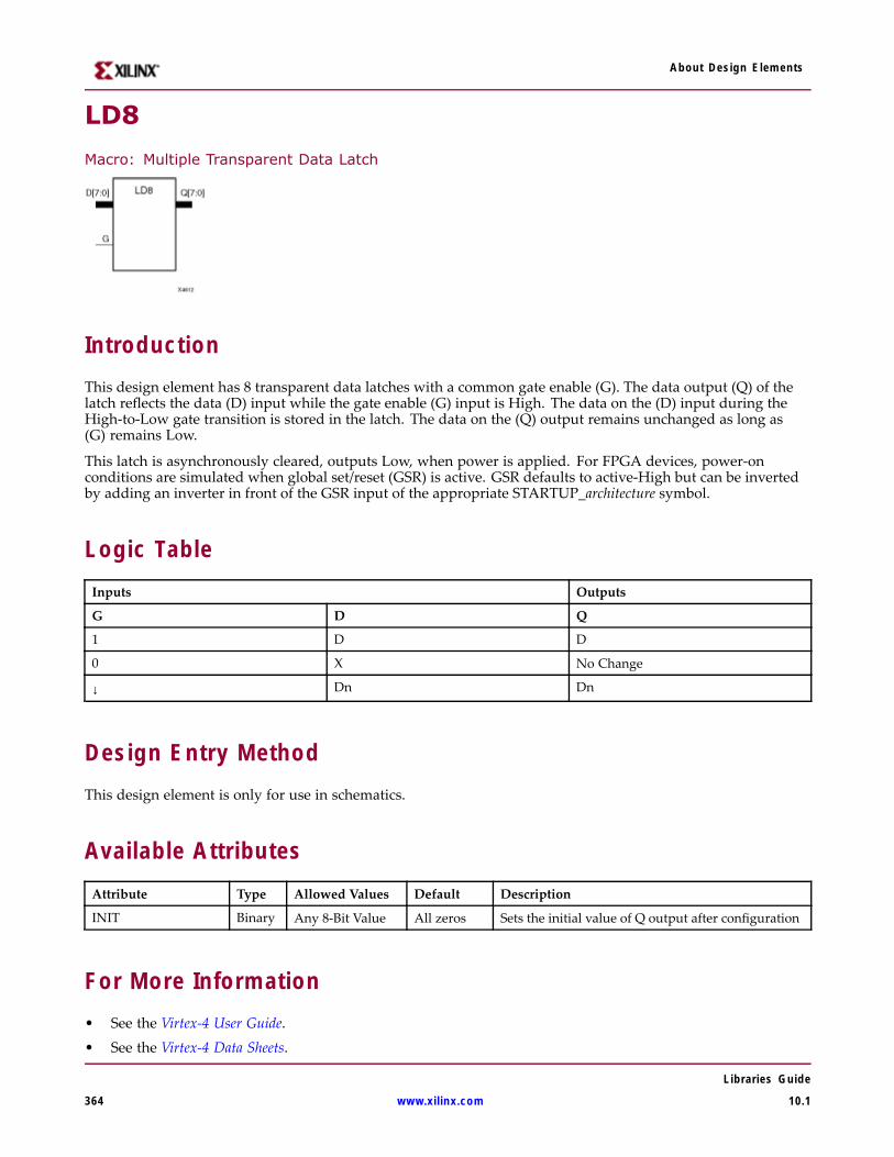
About Design Elements
LD8
Macro: Multiple Transparent Data Latch
IntroductionThis design element has 8 transparent data latches with a common gate enable (G). The data output (Q) of thelatch reflects the data (D) input while the gate enable (G) input is High. The data on the (D) input during theHigh-to-Low gate transition is stored in the latch. The data on the (Q) output remains unchanged as long as(G) remains Low.
This latch is asynchronously cleared, outputs Low, when power is applied. For FPGA devices, power-onconditions are simulated when global set/reset (GSR) is active. GSR defaults to active-High but can be invertedby adding an inverter in front of the GSR input of the appropriate STARTUP_architecture symbol.
Logic TableInputs Outputs
G D Q
1 D D
0 X No Change
↓ Dn Dn
Design Entry MethodThis design element is only for use in schematics.
Available AttributesAttribute Type Allowed Values Default Description
INIT Binary Any 8-Bit Value All zeros Sets the initial value of Q output after configuration
For More Information• See the Virtex-4 User Guide.• See the Virtex-4 Data Sheets.
Libraries Guide
364 www.xilinx.com 10.1

About Design Elements
LD8CE
Macro: Transparent Data Latch with Asynchronous Clear and Gate Enable
IntroductionThis design element has 8 transparent data latches with asynchronous clear and gate enable. When theasynchronous clear input (CLR) is High, it overrides the other inputs and resets the data (Q) outputs Low. (Q)reflects the data (D) inputs while the gate (G) and gate enable (GE) are High, and (CLR) is Low. If (GE) is Low,data on (D) cannot be latched. The data on the (D) input during the High-to-Low gate transition is stored in thelatch. The data on the (Q) output remains unchanged as long as (G) or (GE) remains Low.
This latch is asynchronously cleared, outputs Low, when power is applied. For FPGA devices, power-onconditions are simulated when global set/reset (GSR) is active. GSR defaults to active-High but can be invertedby adding an inverter in front of the GSR input of the appropriate STARTUP_architecture symbol.
Logic TableInputs Outputs
CLR GE G Dn Qn
1 X X X 0
0 0 X X No Change
0 1 1 Dn Dn
0 1 0 X No Change
0 1 ↓ Dn Dn
Dn = referenced input, for example, D0, D1, D2
Qn = referenced output, for example, Q0, Q1, Q2
Design Entry MethodThis design element is only for use in schematics.
Available AttributesAttribute Type Allowed Values Default Description
INIT Binary Any 8-Bit Value All zeros Sets the initial value of Q output afterconfiguration.
Libraries Guide
10.1 www.xilinx.com 365

About Design Elements
For More Information• See the Virtex-4 User Guide.
• See the Virtex-4 Data Sheets.
Libraries Guide
366 www.xilinx.com 10.1
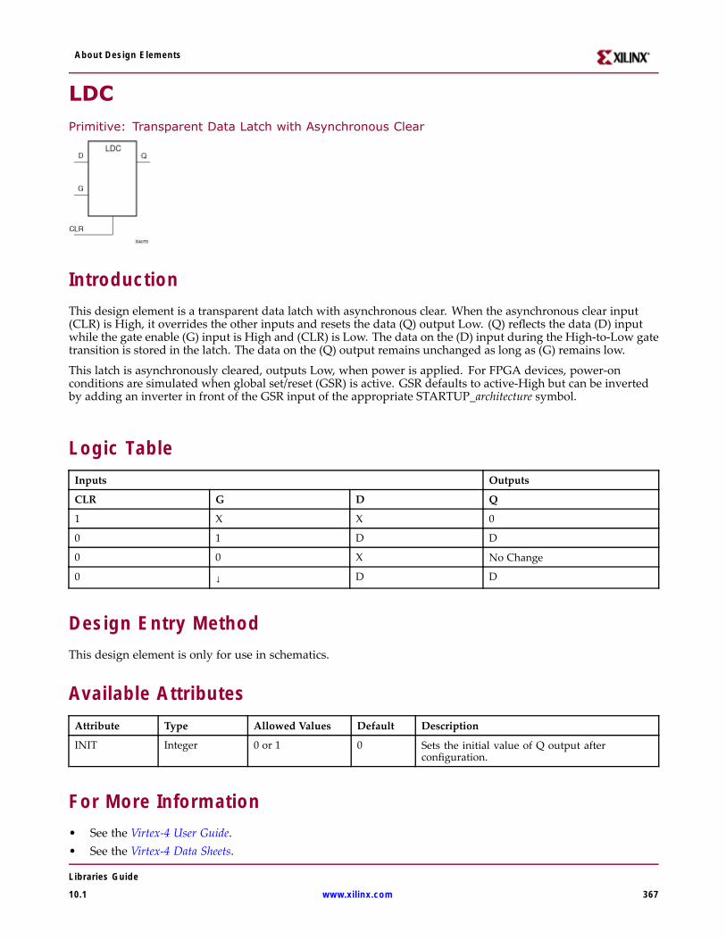
About Design Elements
LDCPrimitive: Transparent Data Latch with Asynchronous Clear
IntroductionThis design element is a transparent data latch with asynchronous clear. When the asynchronous clear input(CLR) is High, it overrides the other inputs and resets the data (Q) output Low. (Q) reflects the data (D) inputwhile the gate enable (G) input is High and (CLR) is Low. The data on the (D) input during the High-to-Low gatetransition is stored in the latch. The data on the (Q) output remains unchanged as long as (G) remains low.
This latch is asynchronously cleared, outputs Low, when power is applied. For FPGA devices, power-onconditions are simulated when global set/reset (GSR) is active. GSR defaults to active-High but can be invertedby adding an inverter in front of the GSR input of the appropriate STARTUP_architecture symbol.
Logic TableInputs Outputs
CLR G D Q
1 X X 0
0 1 D D
0 0 X No Change
0 ↓ D D
Design Entry MethodThis design element is only for use in schematics.
Available AttributesAttribute Type Allowed Values Default Description
INIT Integer 0 or 1 0 Sets the initial value of Q output afterconfiguration.
For More Information• See the Virtex-4 User Guide.• See the Virtex-4 Data Sheets.
Libraries Guide
10.1 www.xilinx.com 367
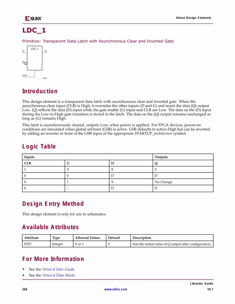
About Design Elements
LDC_1Primitive: Transparent Data Latch with Asynchronous Clear and Inverted Gate
IntroductionThis design element is a transparent data latch with asynchronous clear and inverted gate. When theasynchronous clear input (CLR) is High, it overrides the other inputs (D and G) and resets the data (Q) outputLow. (Q) reflects the data (D) input while the gate enable (G) input and CLR are Low. The data on the (D) inputduring the Low-to-High gate transition is stored in the latch. The data on the (Q) output remains unchanged aslong as (G) remains High.
This latch is asynchronously cleared, outputs Low, when power is applied. For FPGA devices, power-onconditions are simulated when global set/reset (GSR) is active. GSR defaults to active-High but can be invertedby adding an inverter in front of the GSR input of the appropriate STARTUP_architecture symbol.
Logic TableInputs Outputs
CLR G D Q
1 X X 0
0 0 D D
0 1 X No Change
0 ↑ D D
Design Entry MethodThis design element is only for use in schematics.
Available AttributesAttribute Type Allowed Values Default Description
INIT Integer 0 or 1 0 Sets the initial value of Q output after configuration.
For More Information• See the Virtex-4 User Guide.• See the Virtex-4 Data Sheets.
Libraries Guide
368 www.xilinx.com 10.1
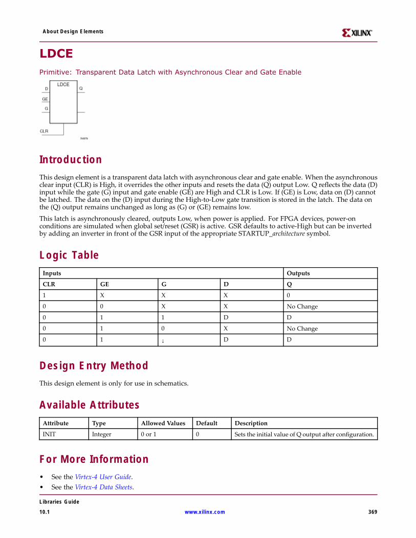
About Design Elements
LDCEPrimitive: Transparent Data Latch with Asynchronous Clear and Gate Enable
IntroductionThis design element is a transparent data latch with asynchronous clear and gate enable. When the asynchronousclear input (CLR) is High, it overrides the other inputs and resets the data (Q) output Low. Q reflects the data (D)input while the gate (G) input and gate enable (GE) are High and CLR is Low. If (GE) is Low, data on (D) cannotbe latched. The data on the (D) input during the High-to-Low gate transition is stored in the latch. The data onthe (Q) output remains unchanged as long as (G) or (GE) remains low.
This latch is asynchronously cleared, outputs Low, when power is applied. For FPGA devices, power-onconditions are simulated when global set/reset (GSR) is active. GSR defaults to active-High but can be invertedby adding an inverter in front of the GSR input of the appropriate STARTUP_architecture symbol.
Logic TableInputs Outputs
CLR GE G D Q
1 X X X 0
0 0 X X No Change
0 1 1 D D
0 1 0 X No Change
0 1 ↓ D D
Design Entry MethodThis design element is only for use in schematics.
Available AttributesAttribute Type Allowed Values Default Description
INIT Integer 0 or 1 0 Sets the initial value of Q output after configuration.
For More Information• See the Virtex-4 User Guide.• See the Virtex-4 Data Sheets.
Libraries Guide
10.1 www.xilinx.com 369
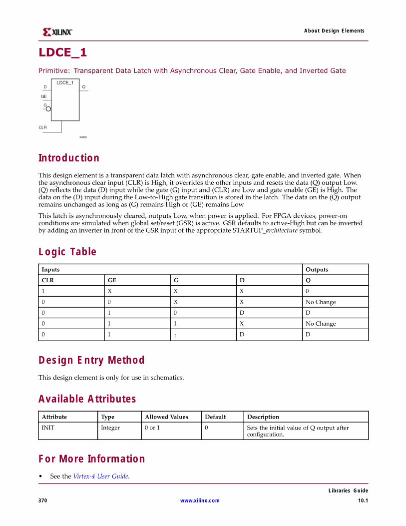
About Design Elements
LDCE_1Primitive: Transparent Data Latch with Asynchronous Clear, Gate Enable, and Inverted Gate
IntroductionThis design element is a transparent data latch with asynchronous clear, gate enable, and inverted gate. Whenthe asynchronous clear input (CLR) is High, it overrides the other inputs and resets the data (Q) output Low.(Q) reflects the data (D) input while the gate (G) input and (CLR) are Low and gate enable (GE) is High. Thedata on the (D) input during the Low-to-High gate transition is stored in the latch. The data on the (Q) outputremains unchanged as long as (G) remains High or (GE) remains Low
This latch is asynchronously cleared, outputs Low, when power is applied. For FPGA devices, power-onconditions are simulated when global set/reset (GSR) is active. GSR defaults to active-High but can be invertedby adding an inverter in front of the GSR input of the appropriate STARTUP_architecture symbol.
Logic TableInputs Outputs
CLR GE G D Q
1 X X X 0
0 0 X X No Change
0 1 0 D D
0 1 1 X No Change
0 1 ↑ D D
Design Entry MethodThis design element is only for use in schematics.
Available AttributesAttribute Type Allowed Values Default Description
INIT Integer 0 or 1 0 Sets the initial value of Q output afterconfiguration.
For More Information• See the Virtex-4 User Guide.
Libraries Guide
370 www.xilinx.com 10.1

About Design Elements
• See the Virtex-4 Data Sheets.
Libraries Guide
10.1 www.xilinx.com 371
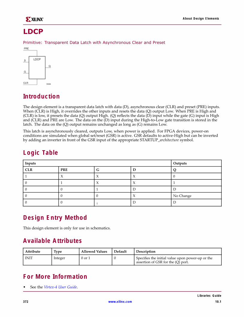
About Design Elements
LDCPPrimitive: Transparent Data Latch with Asynchronous Clear and Preset
IntroductionThe design element is a transparent data latch with data (D), asynchronous clear (CLR) and preset (PRE) inputs.When (CLR) is High, it overrides the other inputs and resets the data (Q) output Low. When PRE is High and(CLR) is low, it presets the data (Q) output High. (Q) reflects the data (D) input while the gate (G) input is Highand (CLR) and PRE are Low. The data on the (D) input during the High-to-Low gate transition is stored in thelatch. The data on the (Q) output remains unchanged as long as (G) remains Low.
This latch is asynchronously cleared, outputs Low, when power is applied. For FPGA devices, power-onconditions are simulated when global set/reset (GSR) is active. GSR defaults to active-High but can be invertedby adding an inverter in front of the GSR input of the appropriate STARTUP_architecture symbol.
Logic TableInputs Outputs
CLR PRE G D Q
1 X X X 0
0 1 X X 1
0 0 1 D D
0 0 0 X No Change
0 0 ↓ D D
Design Entry MethodThis design element is only for use in schematics.
Available AttributesAttribute Type Allowed Values Default Description
INIT Integer 0 or 1 0 Specifies the initial value upon power-up or theassertion of GSR for the (Q) port.
For More Information• See the Virtex-4 User Guide.
Libraries Guide
372 www.xilinx.com 10.1

About Design Elements
• See the Virtex-4 Data Sheets.
Libraries Guide
10.1 www.xilinx.com 373
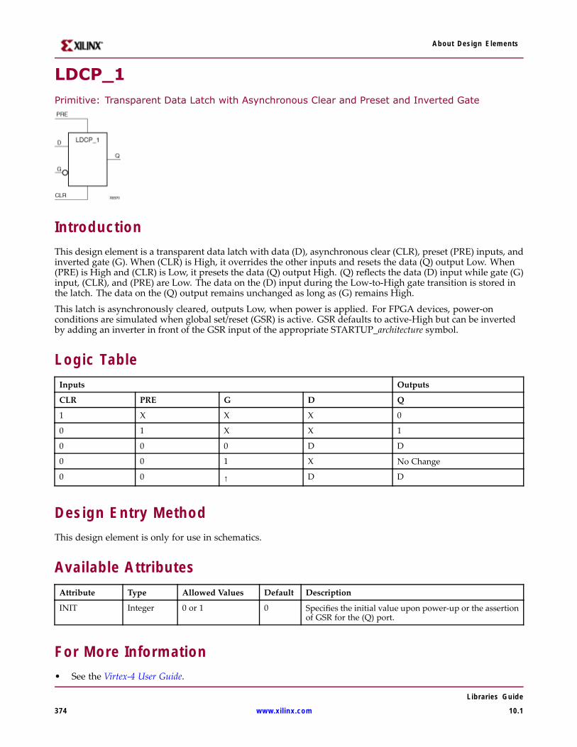
About Design Elements
LDCP_1Primitive: Transparent Data Latch with Asynchronous Clear and Preset and Inverted Gate
IntroductionThis design element is a transparent data latch with data (D), asynchronous clear (CLR), preset (PRE) inputs, andinverted gate (G). When (CLR) is High, it overrides the other inputs and resets the data (Q) output Low. When(PRE) is High and (CLR) is Low, it presets the data (Q) output High. (Q) reflects the data (D) input while gate (G)input, (CLR), and (PRE) are Low. The data on the (D) input during the Low-to-High gate transition is stored inthe latch. The data on the (Q) output remains unchanged as long as (G) remains High.
This latch is asynchronously cleared, outputs Low, when power is applied. For FPGA devices, power-onconditions are simulated when global set/reset (GSR) is active. GSR defaults to active-High but can be invertedby adding an inverter in front of the GSR input of the appropriate STARTUP_architecture symbol.
Logic TableInputs Outputs
CLR PRE G D Q
1 X X X 0
0 1 X X 1
0 0 0 D D
0 0 1 X No Change
0 0 ↑ D D
Design Entry MethodThis design element is only for use in schematics.
Available AttributesAttribute Type Allowed Values Default Description
INIT Integer 0 or 1 0 Specifies the initial value upon power-up or the assertionof GSR for the (Q) port.
For More Information• See the Virtex-4 User Guide.
Libraries Guide
374 www.xilinx.com 10.1

About Design Elements
• See the Virtex-4 Data Sheets.
Libraries Guide
10.1 www.xilinx.com 375
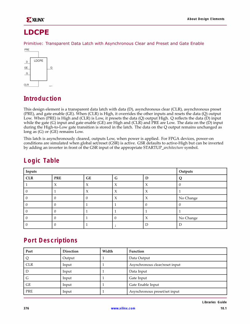
About Design Elements
LDCPEPrimitive: Transparent Data Latch with Asynchronous Clear and Preset and Gate Enable
IntroductionThis design element is a transparent data latch with data (D), asynchronous clear (CLR), asynchronous preset(PRE), and gate enable (GE). When (CLR) is High, it overrides the other inputs and resets the data (Q) outputLow. When (PRE) is High and (CLR) is Low, it presets the data (Q) output High. Q reflects the data (D) inputwhile the gate (G) input and gate enable (GE) are High and (CLR) and PRE are Low. The data on the (D) inputduring the High-to-Low gate transition is stored in the latch. The data on the Q output remains unchanged aslong as (G) or (GE) remains Low.
This latch is asynchronously cleared, outputs Low, when power is applied. For FPGA devices, power-onconditions are simulated when global set/reset (GSR) is active. GSR defaults to active-High but can be invertedby adding an inverter in front of the GSR input of the appropriate STARTUP_architecture symbol.
Logic TableInputs Outputs
CLR PRE GE G D Q
1 X X X X 0
0 1 X X X 1
0 0 0 X X No Change
0 0 1 1 0 0
0 0 1 1 1 1
0 0 1 0 X No Change
0 0 1 ↓ D D
Port DescriptionsPort Direction Width Function
Q Output 1 Data Output
CLR Input 1 Asynchronous clear/reset input
D Input 1 Data Input
G Input 1 Gate Input
GE Input 1 Gate Enable Input
PRE Input 1 Asynchronous preset/set input
Libraries Guide
376 www.xilinx.com 10.1
About Design Elements
Design Entry MethodThis design element can be used in schematics.
Available AttributesAttribute Type Allowed Values Default Description
INIT Integer 0 or 1 0 Sets the initial value of Q output after configuration.
For More Information• See the Virtex-4 User Guide.
• See the Virtex-4 Data Sheets.
Libraries Guide
10.1 www.xilinx.com 377
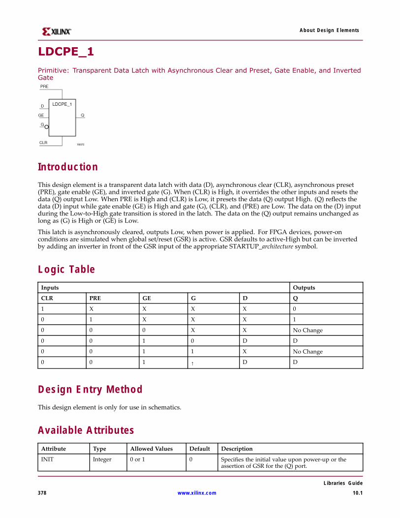
About Design Elements
LDCPE_1
Primitive: Transparent Data Latch with Asynchronous Clear and Preset, Gate Enable, and InvertedGate
IntroductionThis design element is a transparent data latch with data (D), asynchronous clear (CLR), asynchronous preset(PRE), gate enable (GE), and inverted gate (G). When (CLR) is High, it overrides the other inputs and resets thedata (Q) output Low. When PRE is High and (CLR) is Low, it presets the data (Q) output High. (Q) reflects thedata (D) input while gate enable (GE) is High and gate (G), (CLR), and (PRE) are Low. The data on the (D) inputduring the Low-to-High gate transition is stored in the latch. The data on the (Q) output remains unchanged aslong as (G) is High or (GE) is Low.
This latch is asynchronously cleared, outputs Low, when power is applied. For FPGA devices, power-onconditions are simulated when global set/reset (GSR) is active. GSR defaults to active-High but can be invertedby adding an inverter in front of the GSR input of the appropriate STARTUP_architecture symbol.
Logic TableInputs Outputs
CLR PRE GE G D Q
1 X X X X 0
0 1 X X X 1
0 0 0 X X No Change
0 0 1 0 D D
0 0 1 1 X No Change
0 0 1 ↑ D D
Design Entry MethodThis design element is only for use in schematics.
Available AttributesAttribute Type Allowed Values Default Description
INIT Integer 0 or 1 0 Specifies the initial value upon power-up or theassertion of GSR for the (Q) port.
Libraries Guide
378 www.xilinx.com 10.1

About Design Elements
For More Information• See the Virtex-4 User Guide.
• See the Virtex-4 Data Sheets.
Libraries Guide
10.1 www.xilinx.com 379
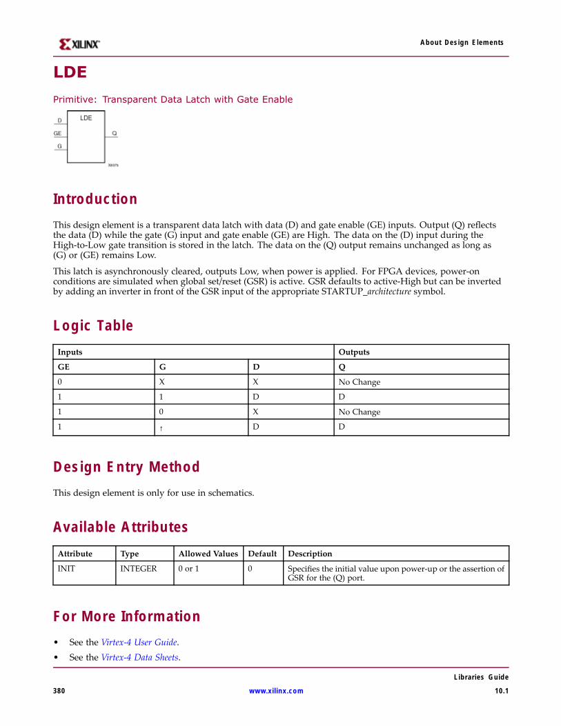
About Design Elements
LDE
Primitive: Transparent Data Latch with Gate Enable
IntroductionThis design element is a transparent data latch with data (D) and gate enable (GE) inputs. Output (Q) reflectsthe data (D) while the gate (G) input and gate enable (GE) are High. The data on the (D) input during theHigh-to-Low gate transition is stored in the latch. The data on the (Q) output remains unchanged as long as(G) or (GE) remains Low.
This latch is asynchronously cleared, outputs Low, when power is applied. For FPGA devices, power-onconditions are simulated when global set/reset (GSR) is active. GSR defaults to active-High but can be invertedby adding an inverter in front of the GSR input of the appropriate STARTUP_architecture symbol.
Logic TableInputs Outputs
GE G D Q
0 X X No Change
1 1 D D
1 0 X No Change
1 ↑ D D
Design Entry MethodThis design element is only for use in schematics.
Available AttributesAttribute Type Allowed Values Default Description
INIT INTEGER 0 or 1 0 Specifies the initial value upon power-up or the assertion ofGSR for the (Q) port.
For More Information• See the Virtex-4 User Guide.• See the Virtex-4 Data Sheets.
Libraries Guide
380 www.xilinx.com 10.1
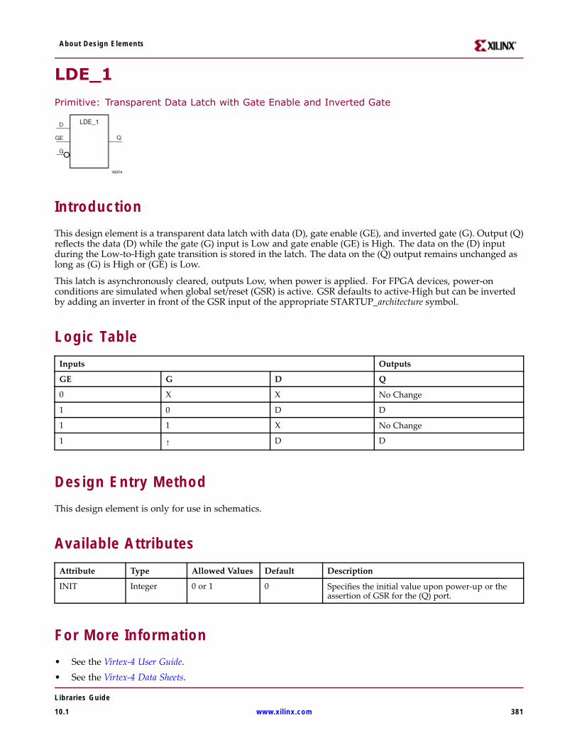
About Design Elements
LDE_1
Primitive: Transparent Data Latch with Gate Enable and Inverted Gate
IntroductionThis design element is a transparent data latch with data (D), gate enable (GE), and inverted gate (G). Output (Q)reflects the data (D) while the gate (G) input is Low and gate enable (GE) is High. The data on the (D) inputduring the Low-to-High gate transition is stored in the latch. The data on the (Q) output remains unchanged aslong as (G) is High or (GE) is Low.
This latch is asynchronously cleared, outputs Low, when power is applied. For FPGA devices, power-onconditions are simulated when global set/reset (GSR) is active. GSR defaults to active-High but can be invertedby adding an inverter in front of the GSR input of the appropriate STARTUP_architecture symbol.
Logic TableInputs Outputs
GE G D Q
0 X X No Change
1 0 D D
1 1 X No Change
1 ↑ D D
Design Entry MethodThis design element is only for use in schematics.
Available AttributesAttribute Type Allowed Values Default Description
INIT Integer 0 or 1 0 Specifies the initial value upon power-up or theassertion of GSR for the (Q) port.
For More Information• See the Virtex-4 User Guide.• See the Virtex-4 Data Sheets.
Libraries Guide
10.1 www.xilinx.com 381
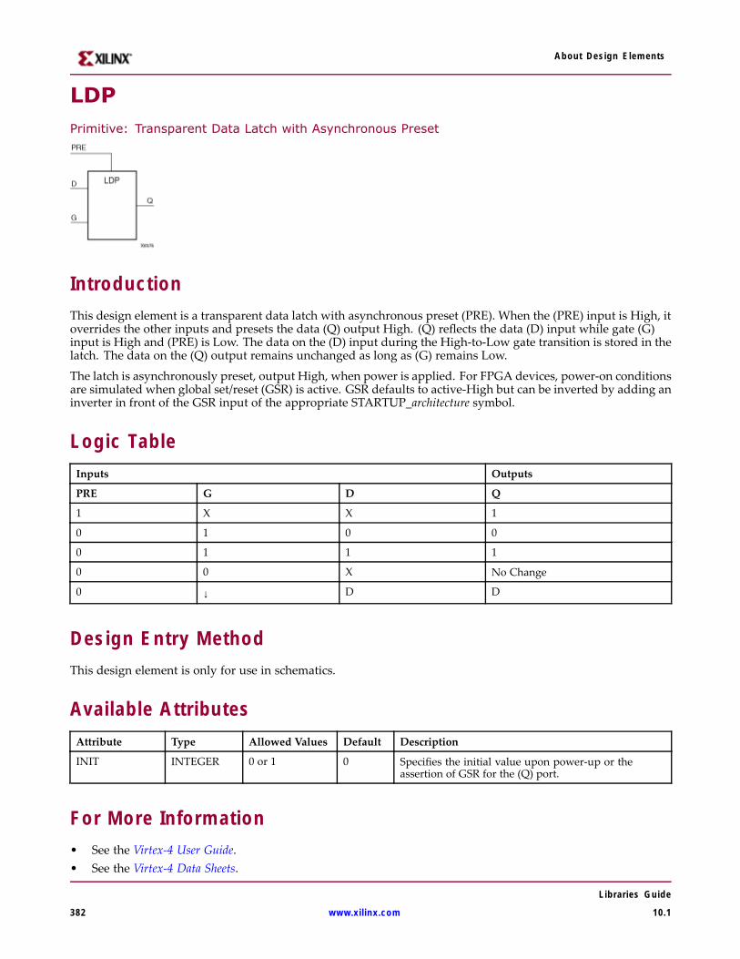
About Design Elements
LDPPrimitive: Transparent Data Latch with Asynchronous Preset
IntroductionThis design element is a transparent data latch with asynchronous preset (PRE). When the (PRE) input is High, itoverrides the other inputs and presets the data (Q) output High. (Q) reflects the data (D) input while gate (G)input is High and (PRE) is Low. The data on the (D) input during the High-to-Low gate transition is stored in thelatch. The data on the (Q) output remains unchanged as long as (G) remains Low.
The latch is asynchronously preset, output High, when power is applied. For FPGA devices, power-on conditionsare simulated when global set/reset (GSR) is active. GSR defaults to active-High but can be inverted by adding aninverter in front of the GSR input of the appropriate STARTUP_architecture symbol.
Logic TableInputs Outputs
PRE G D Q
1 X X 1
0 1 0 0
0 1 1 1
0 0 X No Change
0 ↓ D D
Design Entry MethodThis design element is only for use in schematics.
Available AttributesAttribute Type Allowed Values Default Description
INIT INTEGER 0 or 1 0 Specifies the initial value upon power-up or theassertion of GSR for the (Q) port.
For More Information• See the Virtex-4 User Guide.• See the Virtex-4 Data Sheets.
Libraries Guide
382 www.xilinx.com 10.1
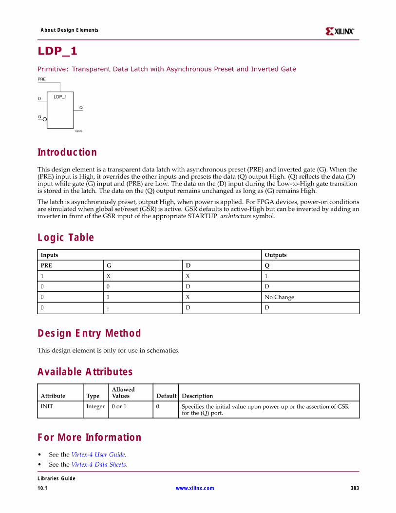
About Design Elements
LDP_1Primitive: Transparent Data Latch with Asynchronous Preset and Inverted Gate
IntroductionThis design element is a transparent data latch with asynchronous preset (PRE) and inverted gate (G). When the(PRE) input is High, it overrides the other inputs and presets the data (Q) output High. (Q) reflects the data (D)input while gate (G) input and (PRE) are Low. The data on the (D) input during the Low-to-High gate transitionis stored in the latch. The data on the (Q) output remains unchanged as long as (G) remains High.
The latch is asynchronously preset, output High, when power is applied. For FPGA devices, power-on conditionsare simulated when global set/reset (GSR) is active. GSR defaults to active-High but can be inverted by adding aninverter in front of the GSR input of the appropriate STARTUP_architecture symbol.
Logic TableInputs Outputs
PRE G D Q
1 X X 1
0 0 D D
0 1 X No Change
0 ↑ D D
Design Entry MethodThis design element is only for use in schematics.
Available Attributes
Attribute TypeAllowedValues Default Description
INIT Integer 0 or 1 0 Specifies the initial value upon power-up or the assertion of GSRfor the (Q) port.
For More Information• See the Virtex-4 User Guide.• See the Virtex-4 Data Sheets.
Libraries Guide
10.1 www.xilinx.com 383
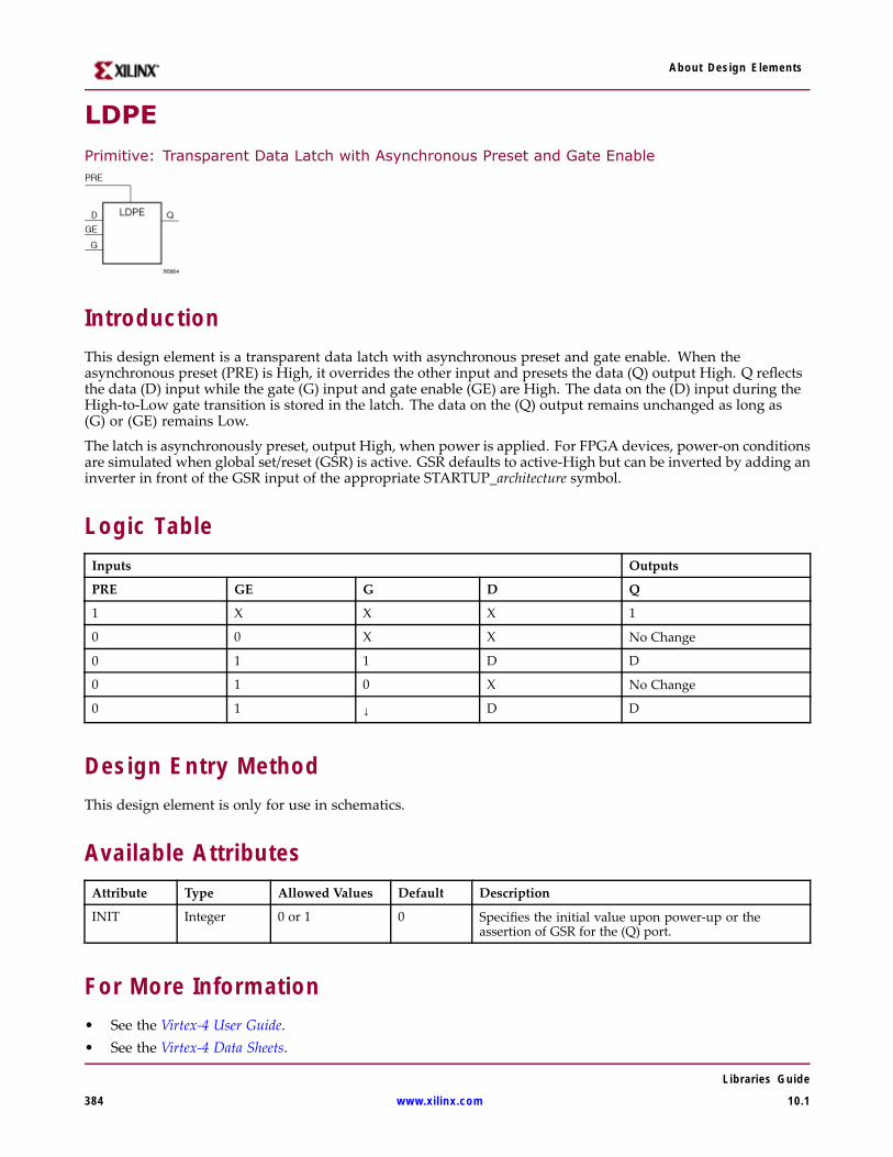
About Design Elements
LDPEPrimitive: Transparent Data Latch with Asynchronous Preset and Gate Enable
IntroductionThis design element is a transparent data latch with asynchronous preset and gate enable. When theasynchronous preset (PRE) is High, it overrides the other input and presets the data (Q) output High. Q reflectsthe data (D) input while the gate (G) input and gate enable (GE) are High. The data on the (D) input during theHigh-to-Low gate transition is stored in the latch. The data on the (Q) output remains unchanged as long as(G) or (GE) remains Low.
The latch is asynchronously preset, output High, when power is applied. For FPGA devices, power-on conditionsare simulated when global set/reset (GSR) is active. GSR defaults to active-High but can be inverted by adding aninverter in front of the GSR input of the appropriate STARTUP_architecture symbol.
Logic TableInputs Outputs
PRE GE G D Q
1 X X X 1
0 0 X X No Change
0 1 1 D D
0 1 0 X No Change
0 1 ↓ D D
Design Entry MethodThis design element is only for use in schematics.
Available AttributesAttribute Type Allowed Values Default Description
INIT Integer 0 or 1 0 Specifies the initial value upon power-up or theassertion of GSR for the (Q) port.
For More Information• See the Virtex-4 User Guide.• See the Virtex-4 Data Sheets.
Libraries Guide
384 www.xilinx.com 10.1
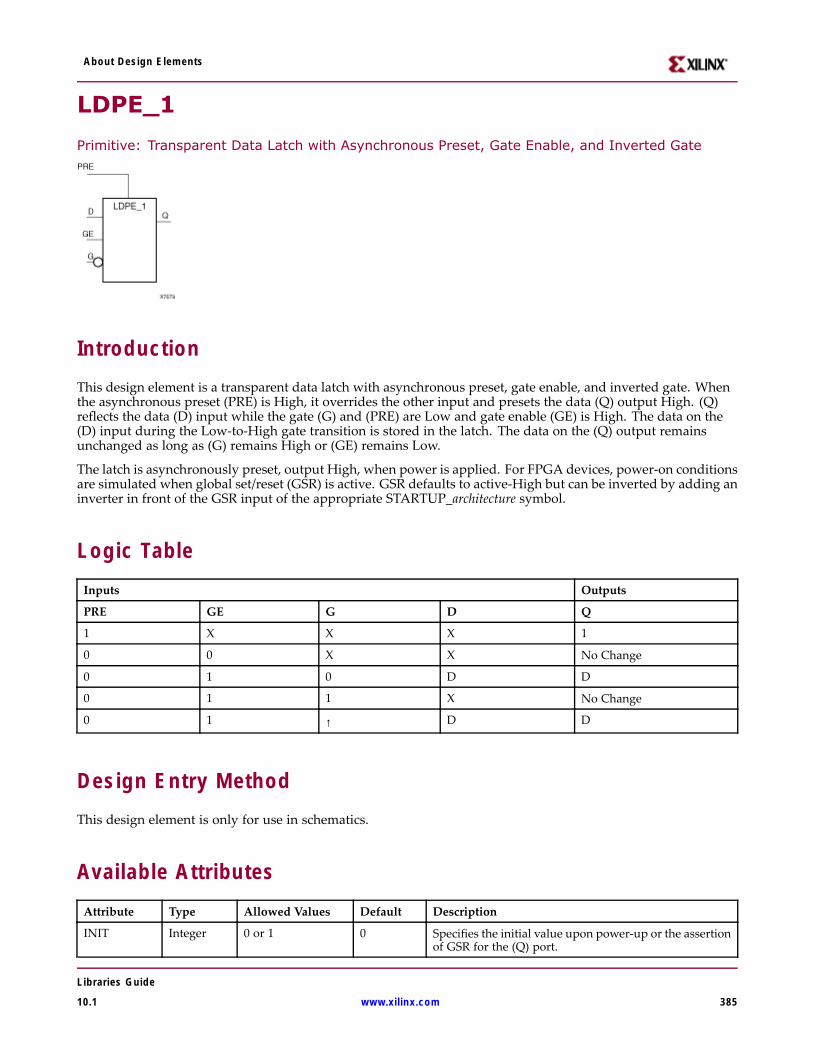
About Design Elements
LDPE_1
Primitive: Transparent Data Latch with Asynchronous Preset, Gate Enable, and Inverted Gate
IntroductionThis design element is a transparent data latch with asynchronous preset, gate enable, and inverted gate. Whenthe asynchronous preset (PRE) is High, it overrides the other input and presets the data (Q) output High. (Q)reflects the data (D) input while the gate (G) and (PRE) are Low and gate enable (GE) is High. The data on the(D) input during the Low-to-High gate transition is stored in the latch. The data on the (Q) output remainsunchanged as long as (G) remains High or (GE) remains Low.
The latch is asynchronously preset, output High, when power is applied. For FPGA devices, power-on conditionsare simulated when global set/reset (GSR) is active. GSR defaults to active-High but can be inverted by adding aninverter in front of the GSR input of the appropriate STARTUP_architecture symbol.
Logic TableInputs Outputs
PRE GE G D Q
1 X X X 1
0 0 X X No Change
0 1 0 D D
0 1 1 X No Change
0 1 ↑ D D
Design Entry MethodThis design element is only for use in schematics.
Available AttributesAttribute Type Allowed Values Default Description
INIT Integer 0 or 1 0 Specifies the initial value upon power-up or the assertionof GSR for the (Q) port.
Libraries Guide
10.1 www.xilinx.com 385

About Design Elements
For More Information• See the Virtex-4 User Guide.
• See the Virtex-4 Data Sheets.
Libraries Guide
386 www.xilinx.com 10.1
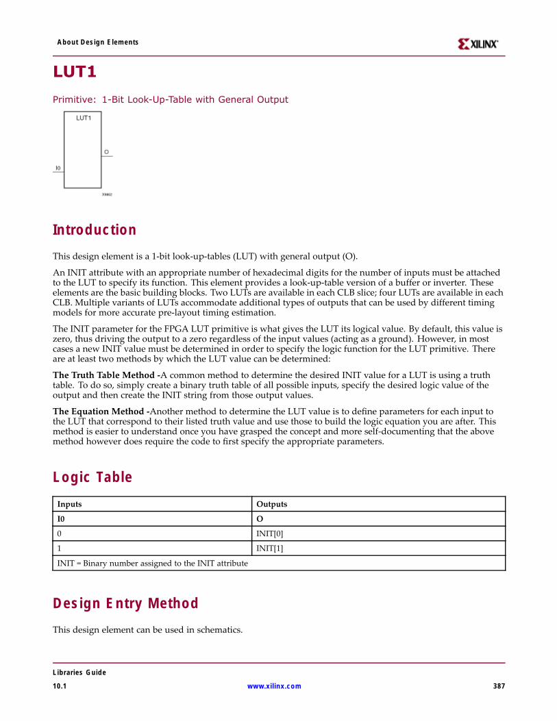
About Design Elements
LUT1
Primitive: 1-Bit Look-Up-Table with General Output
IntroductionThis design element is a 1-bit look-up-tables (LUT) with general output (O).
An INIT attribute with an appropriate number of hexadecimal digits for the number of inputs must be attachedto the LUT to specify its function. This element provides a look-up-table version of a buffer or inverter. Theseelements are the basic building blocks. Two LUTs are available in each CLB slice; four LUTs are available in eachCLB. Multiple variants of LUTs accommodate additional types of outputs that can be used by different timingmodels for more accurate pre-layout timing estimation.
The INIT parameter for the FPGA LUT primitive is what gives the LUT its logical value. By default, this value iszero, thus driving the output to a zero regardless of the input values (acting as a ground). However, in mostcases a new INIT value must be determined in order to specify the logic function for the LUT primitive. Thereare at least two methods by which the LUT value can be determined:
The Truth Table Method -A common method to determine the desired INIT value for a LUT is using a truthtable. To do so, simply create a binary truth table of all possible inputs, specify the desired logic value of theoutput and then create the INIT string from those output values.
The Equation Method -Another method to determine the LUT value is to define parameters for each input tothe LUT that correspond to their listed truth value and use those to build the logic equation you are after. Thismethod is easier to understand once you have grasped the concept and more self-documenting that the abovemethod however does require the code to first specify the appropriate parameters.
Logic TableInputs Outputs
I0 O
0 INIT[0]
1 INIT[1]
INIT = Binary number assigned to the INIT attribute
Design Entry MethodThis design element can be used in schematics.
Libraries Guide
10.1 www.xilinx.com 387
About Design Elements
Available AttributesAttribute Type Allowed Values Default Description
INIT Hexadecimal Any 2-Bit Value All zeros Initializes look-up tables.
For More Information• See the Virtex-4 User Guide.
• See the Virtex-4 Data Sheets.
Libraries Guide
388 www.xilinx.com 10.1
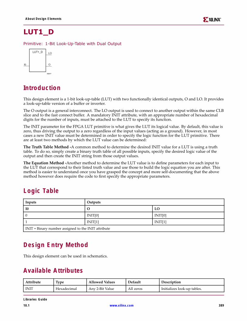
About Design Elements
LUT1_D
Primitive: 1-Bit Look-Up-Table with Dual Output
IntroductionThis design element is a 1-bit look-up-table (LUT) with two functionally identical outputs, O and LO. It providesa look-up-table version of a buffer or inverter.
The O output is a general interconnect. The LO output is used to connect to another output within the same CLBslice and to the fast connect buffer. A mandatory INIT attribute, with an appropriate number of hexadecimaldigits for the number of inputs, must be attached to the LUT to specify its function.
The INIT parameter for the FPGA LUT primitive is what gives the LUT its logical value. By default, this value iszero, thus driving the output to a zero regardless of the input values (acting as a ground). However, in mostcases a new INIT value must be determined in order to specify the logic function for the LUT primitive. Thereare at least two methods by which the LUT value can be determined:
The Truth Table Method -A common method to determine the desired INIT value for a LUT is using a truthtable. To do so, simply create a binary truth table of all possible inputs, specify the desired logic value of theoutput and then create the INIT string from those output values.
The Equation Method -Another method to determine the LUT value is to define parameters for each input tothe LUT that correspond to their listed truth value and use those to build the logic equation you are after. Thismethod is easier to understand once you have grasped the concept and more self-documenting that the abovemethod however does require the code to first specify the appropriate parameters.
Logic TableInputs Outputs
I0 O LO
0 INIT[0] INIT[0]
1 INIT[1] INIT[1]
INIT = Binary number assigned to the INIT attribute
Design Entry MethodThis design element can be used in schematics.
Available AttributesAttribute Type Allowed Values Default Description
INIT Hexadecimal Any 2-Bit Value All zeros Initializes look-up tables.
Libraries Guide
10.1 www.xilinx.com 389

About Design Elements
For More Information• See the Virtex-4 User Guide.
• See the Virtex-4 Data Sheets.
Libraries Guide
390 www.xilinx.com 10.1
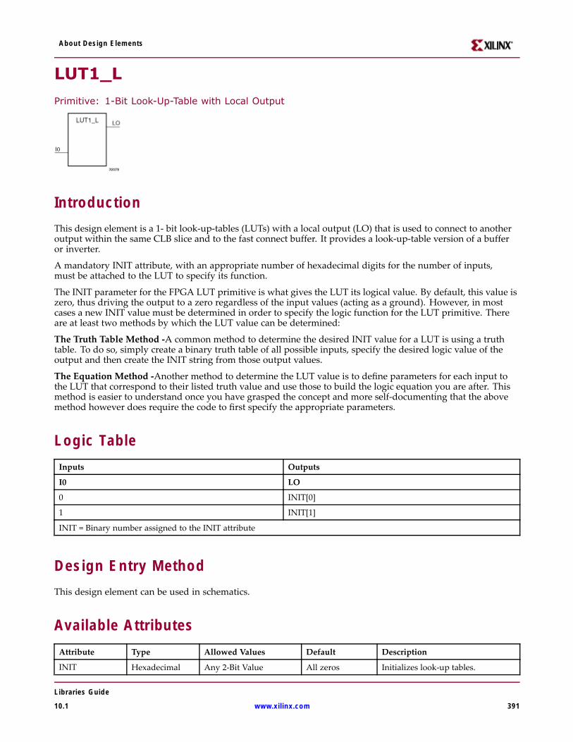
About Design Elements
LUT1_L
Primitive: 1-Bit Look-Up-Table with Local Output
IntroductionThis design element is a 1- bit look-up-tables (LUTs) with a local output (LO) that is used to connect to anotheroutput within the same CLB slice and to the fast connect buffer. It provides a look-up-table version of a bufferor inverter.
A mandatory INIT attribute, with an appropriate number of hexadecimal digits for the number of inputs,must be attached to the LUT to specify its function.
The INIT parameter for the FPGA LUT primitive is what gives the LUT its logical value. By default, this value iszero, thus driving the output to a zero regardless of the input values (acting as a ground). However, in mostcases a new INIT value must be determined in order to specify the logic function for the LUT primitive. Thereare at least two methods by which the LUT value can be determined:
The Truth Table Method -A common method to determine the desired INIT value for a LUT is using a truthtable. To do so, simply create a binary truth table of all possible inputs, specify the desired logic value of theoutput and then create the INIT string from those output values.
The Equation Method -Another method to determine the LUT value is to define parameters for each input tothe LUT that correspond to their listed truth value and use those to build the logic equation you are after. Thismethod is easier to understand once you have grasped the concept and more self-documenting that the abovemethod however does require the code to first specify the appropriate parameters.
Logic TableInputs Outputs
I0 LO
0 INIT[0]
1 INIT[1]
INIT = Binary number assigned to the INIT attribute
Design Entry MethodThis design element can be used in schematics.
Available AttributesAttribute Type Allowed Values Default Description
INIT Hexadecimal Any 2-Bit Value All zeros Initializes look-up tables.
Libraries Guide
10.1 www.xilinx.com 391

About Design Elements
For More Information• See the Virtex-4 User Guide.
• See the Virtex-4 Data Sheets.
Libraries Guide
392 www.xilinx.com 10.1
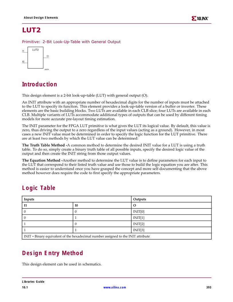
About Design Elements
LUT2
Primitive: 2-Bit Look-Up-Table with General Output
IntroductionThis design element is a 2-bit look-up-table (LUT) with general output (O).
An INIT attribute with an appropriate number of hexadecimal digits for the number of inputs must be attachedto the LUT to specify its function. This element provides a look-up-table version of a buffer or inverter. Theseelements are the basic building blocks. Two LUTs are available in each CLB slice; four LUTs are available in eachCLB. Multiple variants of LUTs accommodate additional types of outputs that can be used by different timingmodels for more accurate pre-layout timing estimation.
The INIT parameter for the FPGA LUT primitive is what gives the LUT its logical value. By default, this value iszero, thus driving the output to a zero regardless of the input values (acting as a ground). However, in mostcases a new INIT value must be determined in order to specify the logic function for the LUT primitive. Thereare at least two methods by which the LUT value can be determined:
The Truth Table Method -A common method to determine the desired INIT value for a LUT is using a truthtable. To do so, simply create a binary truth table of all possible inputs, specify the desired logic value of theoutput and then create the INIT string from those output values.
The Equation Method -Another method to determine the LUT value is to define parameters for each input tothe LUT that correspond to their listed truth value and use those to build the logic equation you are after. Thismethod is easier to understand once you have grasped the concept and more self-documenting that the abovemethod however does require the code to first specify the appropriate parameters.
Logic TableInputs Outputs
I1 I0 O
0 0 INIT[0]
0 1 INIT[1]
1 0 INIT[2]
1 1 INIT[3]
INIT = Binary equivalent of the hexadecimal number assigned to the INIT attribute
Design Entry MethodThis design element can be used in schematics.
Libraries Guide
10.1 www.xilinx.com 393

About Design Elements
Available AttributesAttribute Type Allowed Values Default Description
INIT Hexadecimal Any 4-Bit Value All zeros Initializes look-up tables.
For More Information• See the Virtex-4 User Guide.
• See the Virtex-4 Data Sheets.
Libraries Guide
394 www.xilinx.com 10.1

About Design Elements
LUT2_DPrimitive: 2-Bit Look-Up-Table with Dual Output
IntroductionThis design element is a 2-bit look-up-tables (LUTs) with two functionally identical outputs, O and LO.
The O output is a general interconnect. The LO output is used to connect to another output within the same CLBslice and to the fast connect buffer. A mandatory INIT attribute, with an appropriate number of hexadecimaldigits for the number of inputs, must be attached to the LUT to specify its function.
The INIT parameter for the FPGA LUT primitive is what gives the LUT its logical value. By default, this value iszero, thus driving the output to a zero regardless of the input values (acting as a ground). However, in mostcases a new INIT value must be determined in order to specify the logic function for the LUT primitive. Thereare at least two methods by which the LUT value can be determined:
The Truth Table Method -A common method to determine the desired INIT value for a LUT is using a truthtable. To do so, simply create a binary truth table of all possible inputs, specify the desired logic value of theoutput and then create the INIT string from those output values.
The Equation Method -Another method to determine the LUT value is to define parameters for each input tothe LUT that correspond to their listed truth value and use those to build the logic equation you are after. Thismethod is easier to understand once you have grasped the concept and more self-documenting that the abovemethod however does require the code to first specify the appropriate parameters.
Logic TableInputs Outputs
I1 I0 O LO
0 0 INIT[0] INIT[0]
0 1 INIT[1] INIT[1]
1 0 INIT[2] INIT[2]
1 1 INIT[3] INIT[3]
INIT = Binary equivalent of the hexadecimal number assigned to the INIT attribute
Design Entry MethodThis design element can be used in schematics.
Available AttributesAttribute Type Allowed Values Default Description
INIT Hexadecimal Any 4-Bit Value All zeros Initializes look-up tables.
Libraries Guide
10.1 www.xilinx.com 395

About Design Elements
For More Information• See the Virtex-4 User Guide.
• See the Virtex-4 Data Sheets.
Libraries Guide
396 www.xilinx.com 10.1
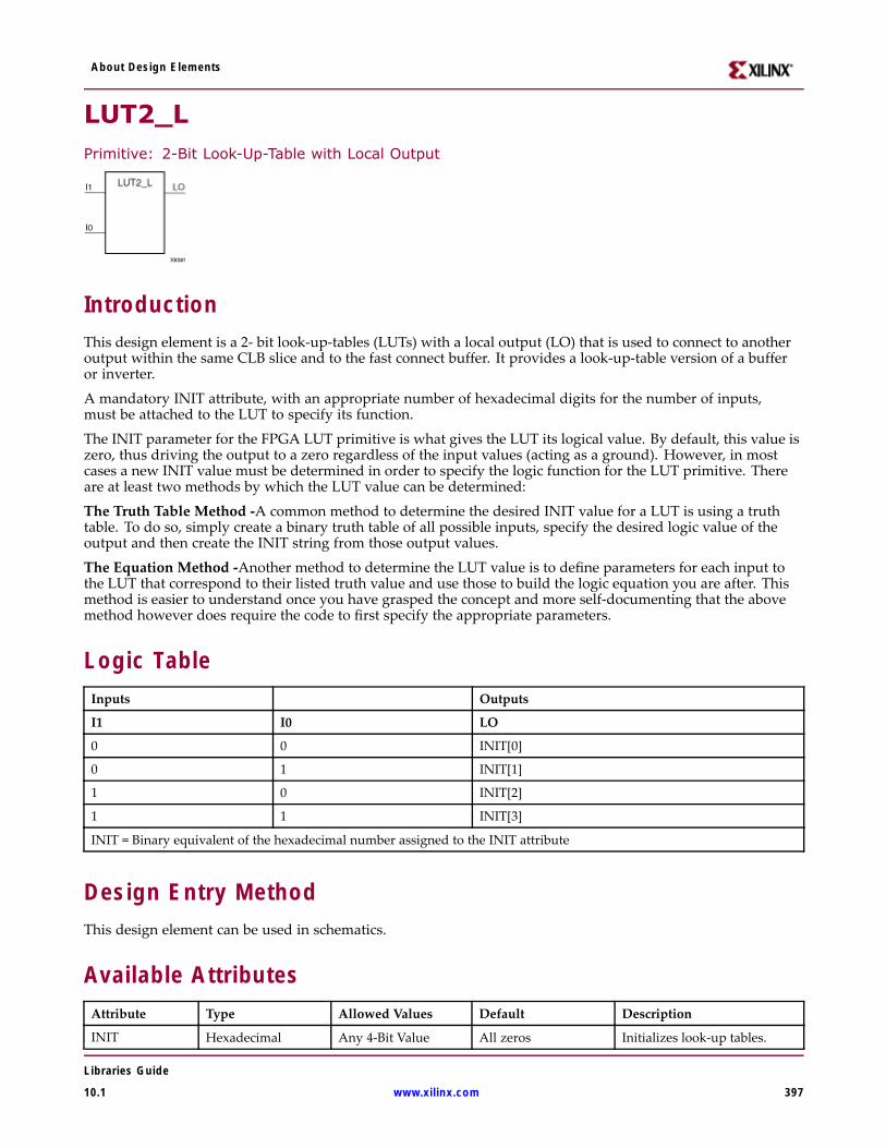
About Design Elements
LUT2_LPrimitive: 2-Bit Look-Up-Table with Local Output
IntroductionThis design element is a 2- bit look-up-tables (LUTs) with a local output (LO) that is used to connect to anotheroutput within the same CLB slice and to the fast connect buffer. It provides a look-up-table version of a bufferor inverter.
A mandatory INIT attribute, with an appropriate number of hexadecimal digits for the number of inputs,must be attached to the LUT to specify its function.
The INIT parameter for the FPGA LUT primitive is what gives the LUT its logical value. By default, this value iszero, thus driving the output to a zero regardless of the input values (acting as a ground). However, in mostcases a new INIT value must be determined in order to specify the logic function for the LUT primitive. Thereare at least two methods by which the LUT value can be determined:
The Truth Table Method -A common method to determine the desired INIT value for a LUT is using a truthtable. To do so, simply create a binary truth table of all possible inputs, specify the desired logic value of theoutput and then create the INIT string from those output values.
The Equation Method -Another method to determine the LUT value is to define parameters for each input tothe LUT that correspond to their listed truth value and use those to build the logic equation you are after. Thismethod is easier to understand once you have grasped the concept and more self-documenting that the abovemethod however does require the code to first specify the appropriate parameters.
Logic TableInputs Outputs
I1 I0 LO
0 0 INIT[0]
0 1 INIT[1]
1 0 INIT[2]
1 1 INIT[3]
INIT = Binary equivalent of the hexadecimal number assigned to the INIT attribute
Design Entry MethodThis design element can be used in schematics.
Available AttributesAttribute Type Allowed Values Default Description
INIT Hexadecimal Any 4-Bit Value All zeros Initializes look-up tables.
Libraries Guide
10.1 www.xilinx.com 397

About Design Elements
For More Information• See the Virtex-4 User Guide.
• See the Virtex-4 Data Sheets.
Libraries Guide
398 www.xilinx.com 10.1
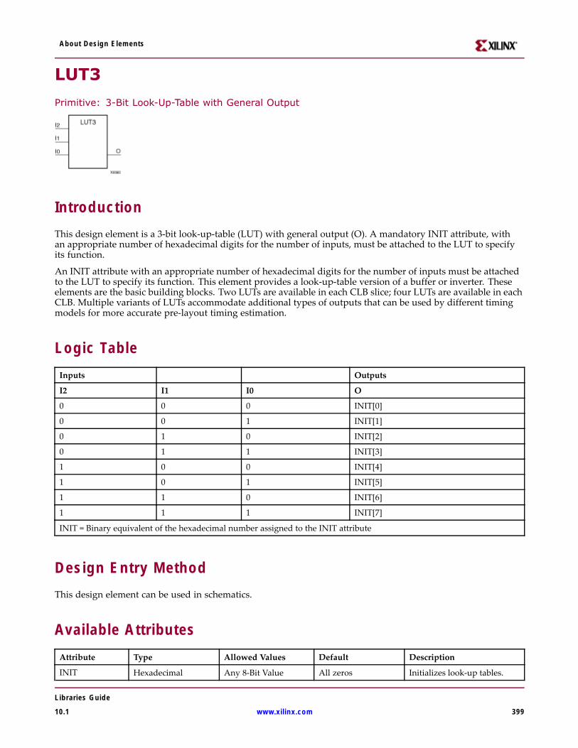
About Design Elements
LUT3
Primitive: 3-Bit Look-Up-Table with General Output
IntroductionThis design element is a 3-bit look-up-table (LUT) with general output (O). A mandatory INIT attribute, withan appropriate number of hexadecimal digits for the number of inputs, must be attached to the LUT to specifyits function.
An INIT attribute with an appropriate number of hexadecimal digits for the number of inputs must be attachedto the LUT to specify its function. This element provides a look-up-table version of a buffer or inverter. Theseelements are the basic building blocks. Two LUTs are available in each CLB slice; four LUTs are available in eachCLB. Multiple variants of LUTs accommodate additional types of outputs that can be used by different timingmodels for more accurate pre-layout timing estimation.
Logic TableInputs Outputs
I2 I1 I0 O
0 0 0 INIT[0]
0 0 1 INIT[1]
0 1 0 INIT[2]
0 1 1 INIT[3]
1 0 0 INIT[4]
1 0 1 INIT[5]
1 1 0 INIT[6]
1 1 1 INIT[7]
INIT = Binary equivalent of the hexadecimal number assigned to the INIT attribute
Design Entry MethodThis design element can be used in schematics.
Available AttributesAttribute Type Allowed Values Default Description
INIT Hexadecimal Any 8-Bit Value All zeros Initializes look-up tables.
Libraries Guide
10.1 www.xilinx.com 399

About Design Elements
For More Information• See the Virtex-4 User Guide.
• See the Virtex-4 Data Sheets.
Libraries Guide
400 www.xilinx.com 10.1
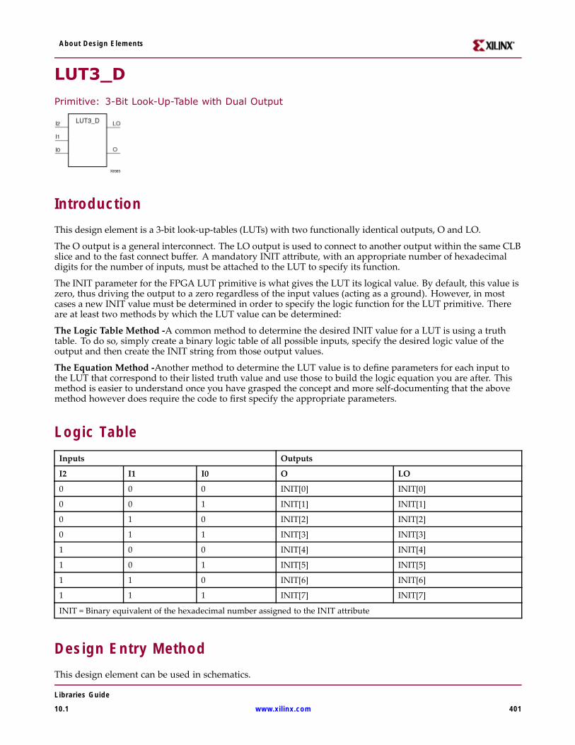
About Design Elements
LUT3_D
Primitive: 3-Bit Look-Up-Table with Dual Output
IntroductionThis design element is a 3-bit look-up-tables (LUTs) with two functionally identical outputs, O and LO.
The O output is a general interconnect. The LO output is used to connect to another output within the same CLBslice and to the fast connect buffer. A mandatory INIT attribute, with an appropriate number of hexadecimaldigits for the number of inputs, must be attached to the LUT to specify its function.
The INIT parameter for the FPGA LUT primitive is what gives the LUT its logical value. By default, this value iszero, thus driving the output to a zero regardless of the input values (acting as a ground). However, in mostcases a new INIT value must be determined in order to specify the logic function for the LUT primitive. Thereare at least two methods by which the LUT value can be determined:
The Logic Table Method -A common method to determine the desired INIT value for a LUT is using a truthtable. To do so, simply create a binary logic table of all possible inputs, specify the desired logic value of theoutput and then create the INIT string from those output values.
The Equation Method -Another method to determine the LUT value is to define parameters for each input tothe LUT that correspond to their listed truth value and use those to build the logic equation you are after. Thismethod is easier to understand once you have grasped the concept and more self-documenting that the abovemethod however does require the code to first specify the appropriate parameters.
Logic TableInputs Outputs
I2 I1 I0 O LO
0 0 0 INIT[0] INIT[0]
0 0 1 INIT[1] INIT[1]
0 1 0 INIT[2] INIT[2]
0 1 1 INIT[3] INIT[3]
1 0 0 INIT[4] INIT[4]
1 0 1 INIT[5] INIT[5]
1 1 0 INIT[6] INIT[6]
1 1 1 INIT[7] INIT[7]
INIT = Binary equivalent of the hexadecimal number assigned to the INIT attribute
Design Entry MethodThis design element can be used in schematics.
Libraries Guide
10.1 www.xilinx.com 401
About Design Elements
Available AttributesAttribute Type Allowed Values Default Description
INIT Hexadecimal Any 8-Bit Value All zeros Initializes look-up tables.
For More Information• See the Virtex-4 User Guide.
• See the Virtex-4 Data Sheets.
Libraries Guide
402 www.xilinx.com 10.1
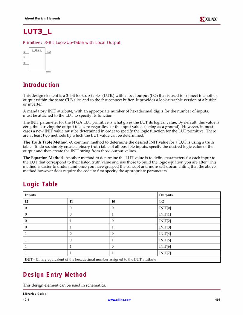
About Design Elements
LUT3_LPrimitive: 3-Bit Look-Up-Table with Local Output
IntroductionThis design element is a 3- bit look-up-tables (LUTs) with a local output (LO) that is used to connect to anotheroutput within the same CLB slice and to the fast connect buffer. It provides a look-up-table version of a bufferor inverter.
A mandatory INIT attribute, with an appropriate number of hexadecimal digits for the number of inputs,must be attached to the LUT to specify its function.
The INIT parameter for the FPGA LUT primitive is what gives the LUT its logical value. By default, this value iszero, thus driving the output to a zero regardless of the input values (acting as a ground). However, in mostcases a new INIT value must be determined in order to specify the logic function for the LUT primitive. Thereare at least two methods by which the LUT value can be determined:
The Truth Table Method -A common method to determine the desired INIT value for a LUT is using a truthtable. To do so, simply create a binary truth table of all possible inputs, specify the desired logic value of theoutput and then create the INIT string from those output values.
The Equation Method -Another method to determine the LUT value is to define parameters for each input tothe LUT that correspond to their listed truth value and use those to build the logic equation you are after. Thismethod is easier to understand once you have grasped the concept and more self-documenting that the abovemethod however does require the code to first specify the appropriate parameters.
Logic TableInputs Outputs
I2 I1 I0 LO
0 0 0 INIT[0]
0 0 1 INIT[1]
0 1 0 INIT[2]
0 1 1 INIT[3]
1 0 0 INIT[4]
1 0 1 INIT[5]
1 1 0 INIT[6]
1 1 1 INIT[7]
INIT = Binary equivalent of the hexadecimal number assigned to the INIT attribute
Design Entry MethodThis design element can be used in schematics.
Libraries Guide
10.1 www.xilinx.com 403

About Design Elements
Available AttributesAttribute Type Allowed Values Default Description
INIT Hexadecimal Any 8-Bit Value All zeros Initializes look-up tables.
For More Information• See the Virtex-4 User Guide.
• See the Virtex-4 Data Sheets.
Libraries Guide
404 www.xilinx.com 10.1
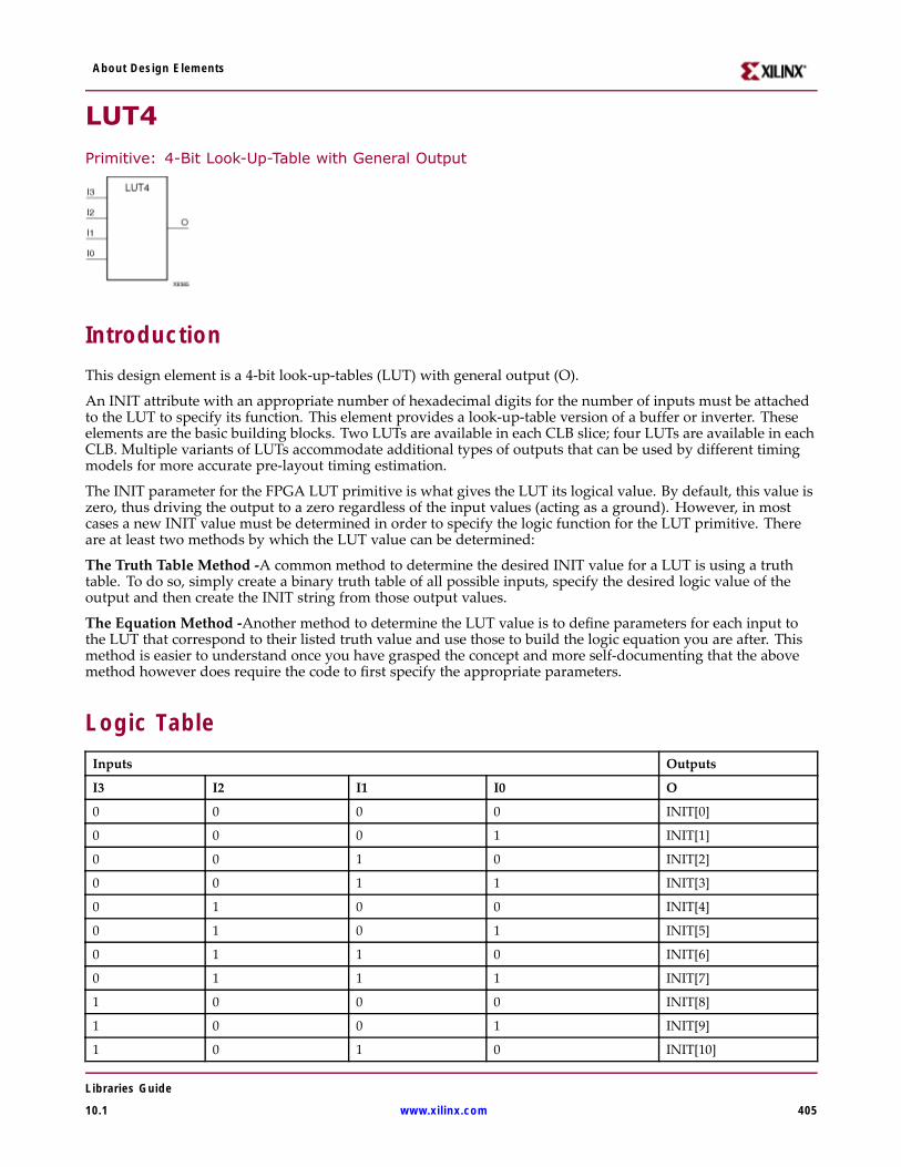
About Design Elements
LUT4
Primitive: 4-Bit Look-Up-Table with General Output
IntroductionThis design element is a 4-bit look-up-tables (LUT) with general output (O).
An INIT attribute with an appropriate number of hexadecimal digits for the number of inputs must be attachedto the LUT to specify its function. This element provides a look-up-table version of a buffer or inverter. Theseelements are the basic building blocks. Two LUTs are available in each CLB slice; four LUTs are available in eachCLB. Multiple variants of LUTs accommodate additional types of outputs that can be used by different timingmodels for more accurate pre-layout timing estimation.
The INIT parameter for the FPGA LUT primitive is what gives the LUT its logical value. By default, this value iszero, thus driving the output to a zero regardless of the input values (acting as a ground). However, in mostcases a new INIT value must be determined in order to specify the logic function for the LUT primitive. Thereare at least two methods by which the LUT value can be determined:
The Truth Table Method -A common method to determine the desired INIT value for a LUT is using a truthtable. To do so, simply create a binary truth table of all possible inputs, specify the desired logic value of theoutput and then create the INIT string from those output values.
The Equation Method -Another method to determine the LUT value is to define parameters for each input tothe LUT that correspond to their listed truth value and use those to build the logic equation you are after. Thismethod is easier to understand once you have grasped the concept and more self-documenting that the abovemethod however does require the code to first specify the appropriate parameters.
Logic TableInputs Outputs
I3 I2 I1 I0 O
0 0 0 0 INIT[0]
0 0 0 1 INIT[1]
0 0 1 0 INIT[2]
0 0 1 1 INIT[3]
0 1 0 0 INIT[4]
0 1 0 1 INIT[5]
0 1 1 0 INIT[6]
0 1 1 1 INIT[7]
1 0 0 0 INIT[8]
1 0 0 1 INIT[9]
1 0 1 0 INIT[10]
Libraries Guide
10.1 www.xilinx.com 405
About Design Elements
Inputs Outputs
I3 I2 I1 I0 O
1 0 1 1 INIT[11]
1 1 0 0 INIT[12]
1 1 0 1 INIT[13]
1 1 1 0 INIT14]
1 1 1 1 INIT[15]
INIT = Binary equivalent of the hexadecimal number assigned to the INIT attribute
Design Entry MethodThis design element can be used in schematics.
Available AttributesAttribute Type Allowed Values Default Description
INIT Hexadecimal Any 16-Bit Value All zeros Initializes look-up tables.
For More Information• See the Virtex-4 User Guide.
• See the Virtex-4 Data Sheets.
Libraries Guide
406 www.xilinx.com 10.1
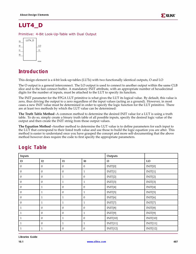
About Design Elements
LUT4_DPrimitive: 4-Bit Look-Up-Table with Dual Output
IntroductionThis design element is a 4-bit look-up-tables (LUTs) with two functionally identical outputs, O and LO
The O output is a general interconnect. The LO output is used to connect to another output within the same CLBslice and to the fast connect buffer. A mandatory INIT attribute, with an appropriate number of hexadecimaldigits for the number of inputs, must be attached to the LUT to specify its function.
The INIT parameter for the FPGA LUT primitive is what gives the LUT its logical value. By default, this value iszero, thus driving the output to a zero regardless of the input values (acting as a ground). However, in mostcases a new INIT value must be determined in order to specify the logic function for the LUT primitive. Thereare at least two methods by which the LUT value can be determined:
The Truth Table Method -A common method to determine the desired INIT value for a LUT is using a truthtable. To do so, simply create a binary truth table of all possible inputs, specify the desired logic value of theoutput and then create the INIT string from those output values.
The Equation Method -Another method to determine the LUT value is to define parameters for each input tothe LUT that correspond to their listed truth value and use those to build the logic equation you are after. Thismethod is easier to understand once you have grasped the concept and more self-documenting that the abovemethod however does require the code to first specify the appropriate parameters.
Logic TableInputs Outputs
I3 I2 I1 I0 O LO
0 0 0 0 INIT[0] INIT[0]
0 0 0 1 INIT[1] INIT[1]
0 0 1 0 INIT[2] INIT[2]
0 0 1 1 INIT[3] INIT[3]
0 1 0 0 INIT[4] INIT[4]
0 1 0 1 INIT[5] INIT[5]
0 1 1 0 INIT[6] INIT[6]
0 1 1 1 INIT[7] INIT[7]
1 0 0 0 INIT[8] INIT[8]
1 0 0 1 INIT[9] INIT[9]
1 0 1 0 INIT[10] INIT[10]
1 0 1 1 INIT[11] INIT[11]
1 1 0 0 INIT[12] INIT[12]
Libraries Guide
10.1 www.xilinx.com 407
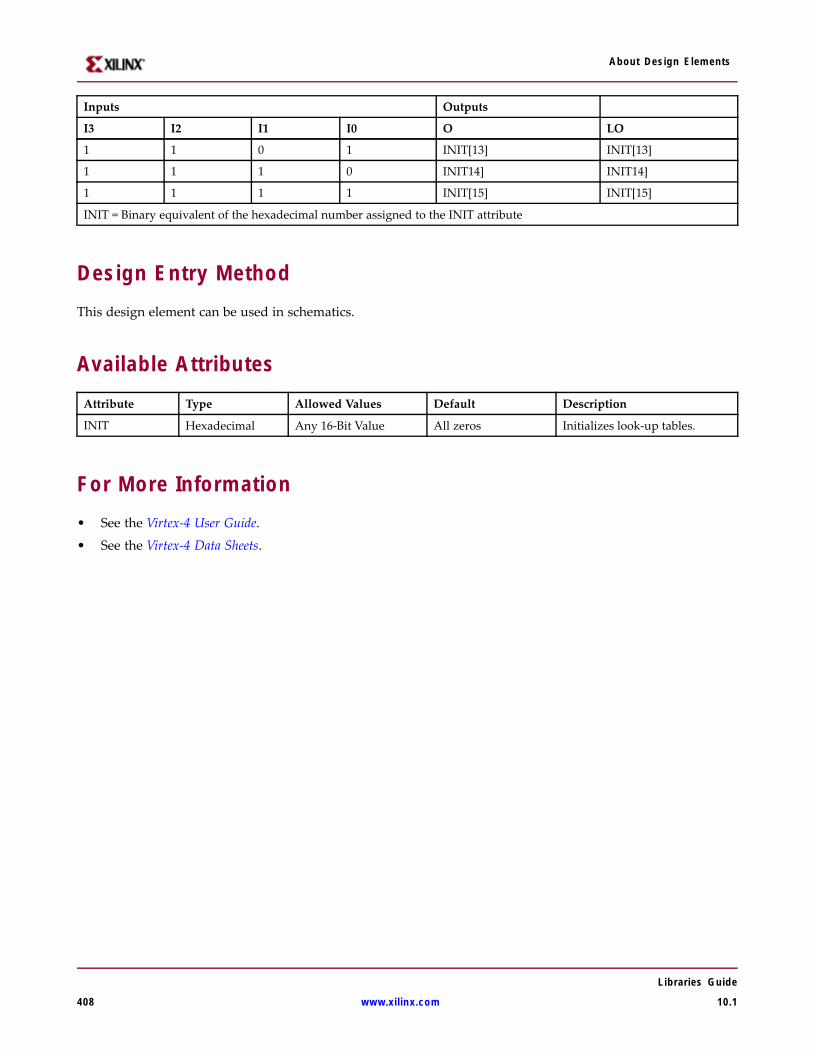
About Design Elements
Inputs Outputs
I3 I2 I1 I0 O LO
1 1 0 1 INIT[13] INIT[13]
1 1 1 0 INIT14] INIT14]
1 1 1 1 INIT[15] INIT[15]
INIT = Binary equivalent of the hexadecimal number assigned to the INIT attribute
Design Entry MethodThis design element can be used in schematics.
Available AttributesAttribute Type Allowed Values Default Description
INIT Hexadecimal Any 16-Bit Value All zeros Initializes look-up tables.
For More Information• See the Virtex-4 User Guide.
• See the Virtex-4 Data Sheets.
Libraries Guide
408 www.xilinx.com 10.1

About Design Elements
LUT4_LPrimitive: 4-Bit Look-Up-Table with Local Output
IntroductionThis design element is a 4- bit look-up-tables (LUTs) with a local output (LO) that is used to connect to anotheroutput within the same CLB slice and to the fast connect buffer. It provides a look-up-table version of a bufferor inverter.
A mandatory INIT attribute, with an appropriate number of hexadecimal digits for the number of inputs,must be attached to the LUT to specify its function.
The INIT parameter for the FPGA LUT primitive is what gives the LUT its logical value. By default, this value iszero, thus driving the output to a zero regardless of the input values (acting as a ground). However, in mostcases a new INIT value must be determined in order to specify the logic function for the LUT primitive. Thereare at least two methods by which the LUT value can be determined:
The Truth Table Method -A common method to determine the desired INIT value for a LUT is using a truthtable. To do so, simply create a binary truth table of all possible inputs, specify the desired logic value of theoutput and then create the INIT string from those output values.
The Equation Method -Another method to determine the LUT value is to define parameters for each input tothe LUT that correspond to their listed truth value and use those to build the logic equation you are after. Thismethod is easier to understand once you have grasped the concept and more self-documenting that the abovemethod however does require the code to first specify the appropriate parameters.
Logic TableInputs Outputs
I3 I2 I1 I0 LO
0 0 0 0 INIT[0]
0 0 0 1 INIT[1]
0 0 1 0 INIT[2]
0 0 1 1 INIT[3]
0 1 0 0 INIT[4]
0 1 0 1 INIT[5]
0 1 1 0 INIT[6]
0 1 1 1 INIT[7]
1 0 0 0 INIT[8]
1 0 0 1 INIT[9]
1 0 1 0 INIT[10]
1 0 1 1 INIT[11]
1 1 0 0 INIT[12]
Libraries Guide
10.1 www.xilinx.com 409
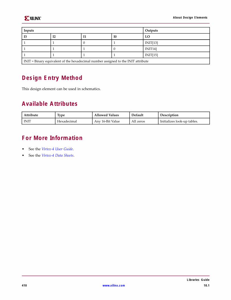
About Design Elements
Inputs Outputs
I3 I2 I1 I0 LO
1 1 0 1 INIT[13]
1 1 1 0 INIT14]
1 1 1 1 INIT[15]
INIT = Binary equivalent of the hexadecimal number assigned to the INIT attribute
Design Entry MethodThis design element can be used in schematics.
Available AttributesAttribute Type Allowed Values Default Description
INIT Hexadecimal Any 16-Bit Value All zeros Initializes look-up tables.
For More Information• See the Virtex-4 User Guide.
• See the Virtex-4 Data Sheets.
Libraries Guide
410 www.xilinx.com 10.1
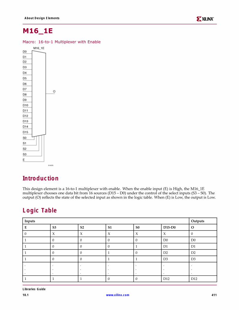
About Design Elements
M16_1EMacro: 16-to-1 Multiplexer with Enable
IntroductionThis design element is a 16-to-1 multiplexer with enable. When the enable input (E) is High, the M16_1Emultiplexer chooses one data bit from 16 sources (D15 – D0) under the control of the select inputs (S3 – S0). Theoutput (O) reflects the state of the selected input as shown in the logic table. When (E) is Low, the output is Low.
Logic TableInputs Outputs
E S3 S2 S1 S0 D15-D0 O
0 X X X X X 0
1 0 0 0 0 D0 D0
1 0 0 0 1 D1 D1
1 0 0 1 0 D2 D2
1 0 0 1 1 D3 D3...
.
.
.
.
.
.
.
.
.
.
.
.
.
.
.
.
.
.
1 1 1 0 0 D12 D12
Libraries Guide
10.1 www.xilinx.com 411
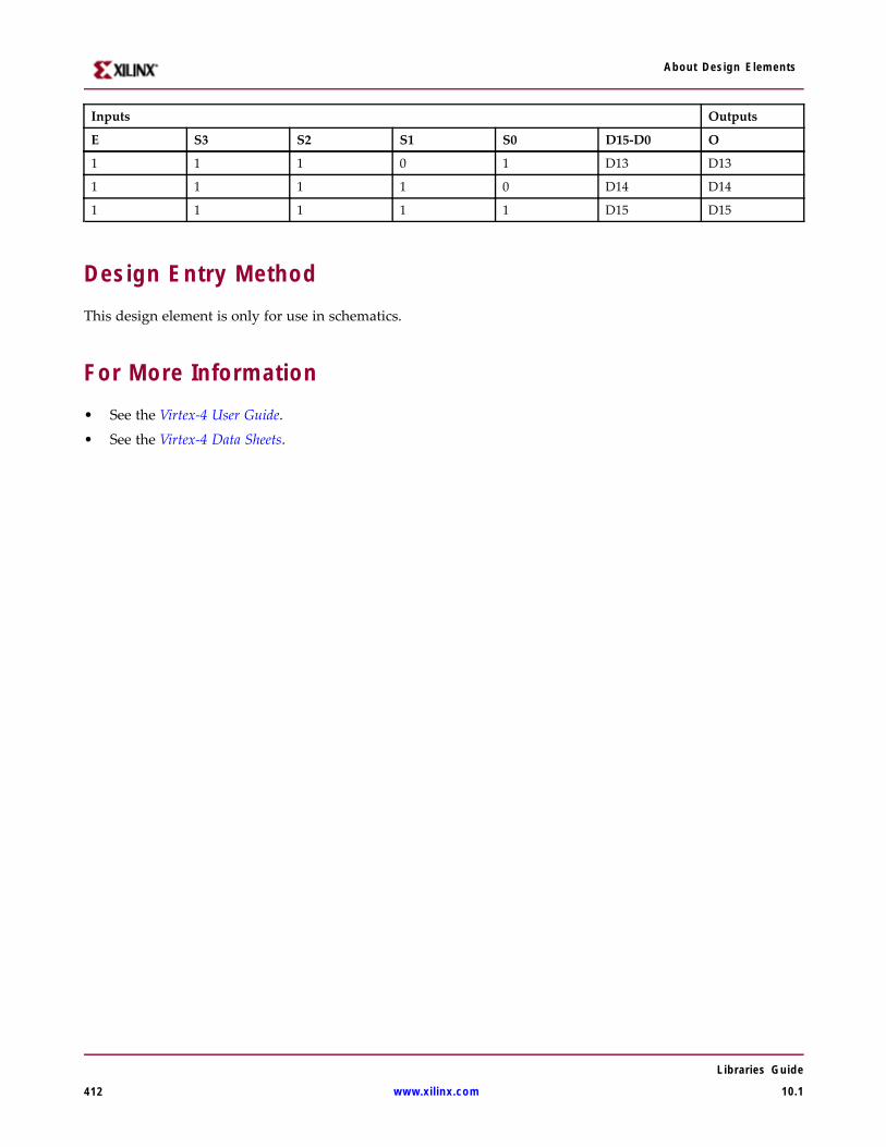
About Design Elements
Inputs Outputs
E S3 S2 S1 S0 D15-D0 O
1 1 1 0 1 D13 D13
1 1 1 1 0 D14 D14
1 1 1 1 1 D15 D15
Design Entry MethodThis design element is only for use in schematics.
For More Information• See the Virtex-4 User Guide.
• See the Virtex-4 Data Sheets.
Libraries Guide
412 www.xilinx.com 10.1
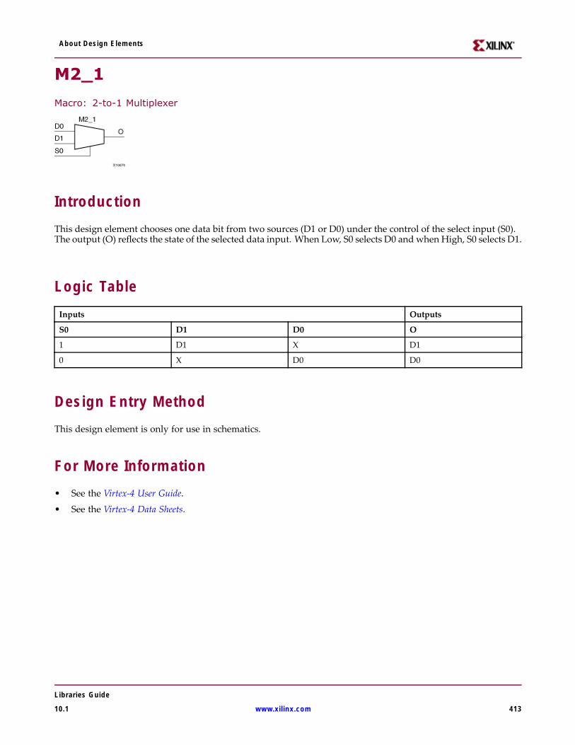
About Design Elements
M2_1
Macro: 2-to-1 Multiplexer
IntroductionThis design element chooses one data bit from two sources (D1 or D0) under the control of the select input (S0).The output (O) reflects the state of the selected data input. When Low, S0 selects D0 and when High, S0 selects D1.
Logic TableInputs Outputs
S0 D1 D0 O
1 D1 X D1
0 X D0 D0
Design Entry MethodThis design element is only for use in schematics.
For More Information• See the Virtex-4 User Guide.
• See the Virtex-4 Data Sheets.
Libraries Guide
10.1 www.xilinx.com 413
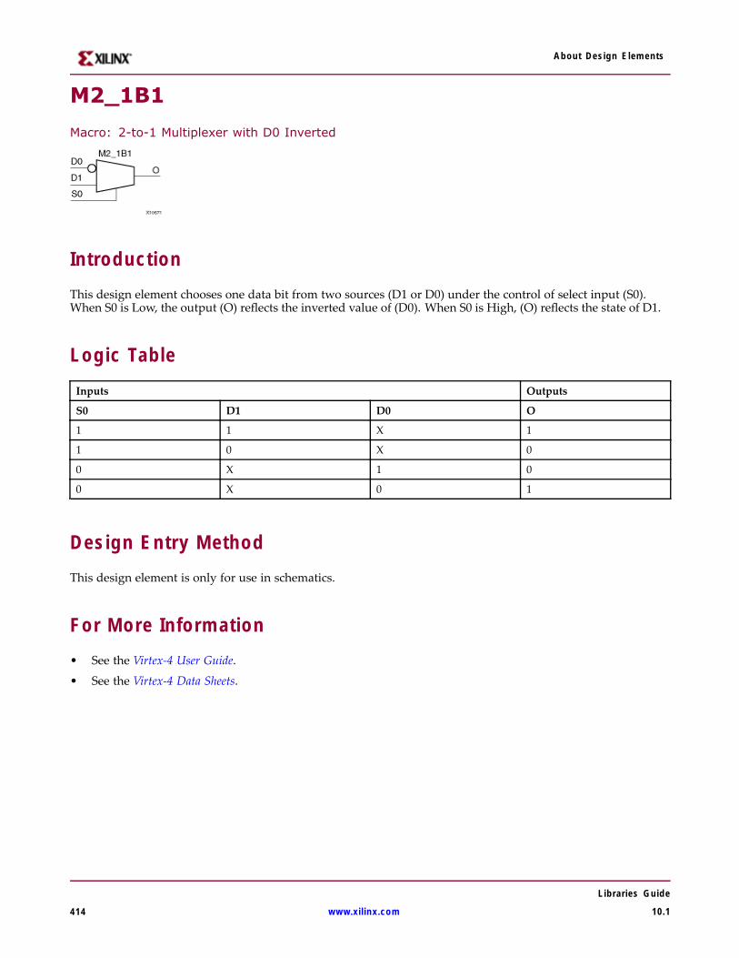
About Design Elements
M2_1B1
Macro: 2-to-1 Multiplexer with D0 Inverted
IntroductionThis design element chooses one data bit from two sources (D1 or D0) under the control of select input (S0).When S0 is Low, the output (O) reflects the inverted value of (D0). When S0 is High, (O) reflects the state of D1.
Logic TableInputs Outputs
S0 D1 D0 O
1 1 X 1
1 0 X 0
0 X 1 0
0 X 0 1
Design Entry MethodThis design element is only for use in schematics.
For More Information• See the Virtex-4 User Guide.
• See the Virtex-4 Data Sheets.
Libraries Guide
414 www.xilinx.com 10.1

About Design Elements
M2_1B2
Macro: 2-to-1 Multiplexer with D0 and D1 Inverted
IntroductionThis design element chooses one data bit from two sources (D1 or D0) under the control of select input (S0). WhenS0 is Low, the output (O) reflects the inverted value of D0. When S0 is High, O reflects the inverted value of D1.
Logic TableInputs Outputs
S0 D1 D0 O
1 1 X 0
1 0 X 1
0 X 1 0
0 X 0 1
Design Entry MethodThis design element is only for use in schematics.
For More Information• See the Virtex-4 User Guide.
• See the Virtex-4 Data Sheets.
Libraries Guide
10.1 www.xilinx.com 415
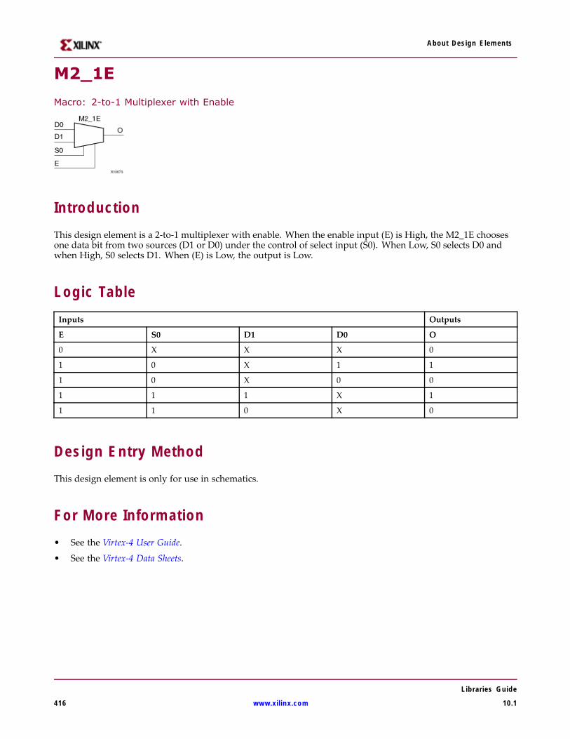
About Design Elements
M2_1E
Macro: 2-to-1 Multiplexer with Enable
IntroductionThis design element is a 2-to-1 multiplexer with enable. When the enable input (E) is High, the M2_1E choosesone data bit from two sources (D1 or D0) under the control of select input (S0). When Low, S0 selects D0 andwhen High, S0 selects D1. When (E) is Low, the output is Low.
Logic TableInputs Outputs
E S0 D1 D0 O
0 X X X 0
1 0 X 1 1
1 0 X 0 0
1 1 1 X 1
1 1 0 X 0
Design Entry MethodThis design element is only for use in schematics.
For More Information• See the Virtex-4 User Guide.
• See the Virtex-4 Data Sheets.
Libraries Guide
416 www.xilinx.com 10.1
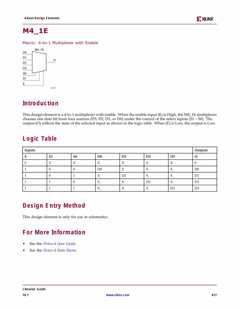
About Design Elements
M4_1E
Macro: 4-to-1 Multiplexer with Enable
IntroductionThis design element is a 4-to-1 multiplexer with enable. When the enable input (E) is High, the M4_1Emultiplexerchooses one data bit from four sources (D3, D2, D1, or D0) under the control of the select inputs (S1 – S0). Theoutput (O) reflects the state of the selected input as shown in the logic table. When (E) is Low, the output is Low.
Logic TableInputs Outputs
E S1 S0 D0 D1 D2 D3 O
0 X X X X X X 0
1 0 0 D0 X X X D0
1 0 1 X D1 X X D1
1 1 0 X X D2 X D2
1 1 1 X X X D3 D3
Design Entry MethodThis design element is only for use in schematics.
For More Information• See the Virtex-4 User Guide.
• See the Virtex-4 Data Sheets.
Libraries Guide
10.1 www.xilinx.com 417
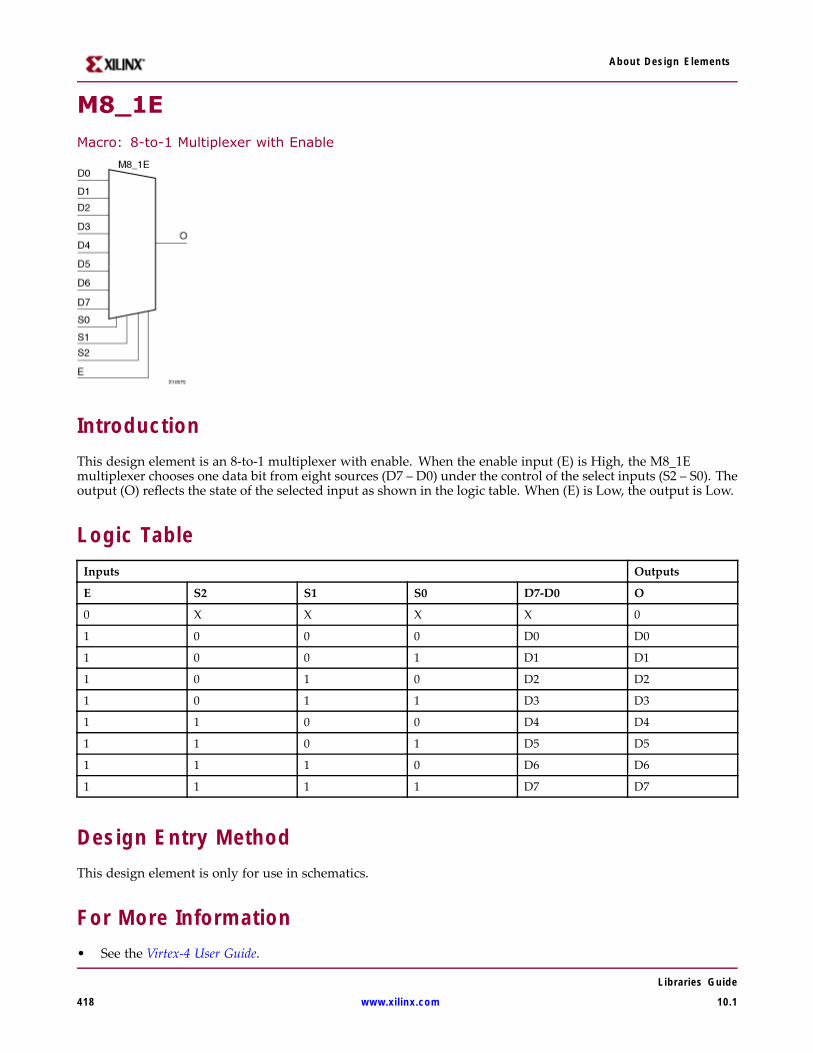
About Design Elements
M8_1EMacro: 8-to-1 Multiplexer with Enable
IntroductionThis design element is an 8-to-1 multiplexer with enable. When the enable input (E) is High, the M8_1Emultiplexer chooses one data bit from eight sources (D7 – D0) under the control of the select inputs (S2 – S0). Theoutput (O) reflects the state of the selected input as shown in the logic table. When (E) is Low, the output is Low.
Logic TableInputs Outputs
E S2 S1 S0 D7-D0 O
0 X X X X 0
1 0 0 0 D0 D0
1 0 0 1 D1 D1
1 0 1 0 D2 D2
1 0 1 1 D3 D3
1 1 0 0 D4 D4
1 1 0 1 D5 D5
1 1 1 0 D6 D6
1 1 1 1 D7 D7
Design Entry MethodThis design element is only for use in schematics.
For More Information• See the Virtex-4 User Guide.
Libraries Guide
418 www.xilinx.com 10.1

About Design Elements
• See the Virtex-4 Data Sheets.
Libraries Guide
10.1 www.xilinx.com 419
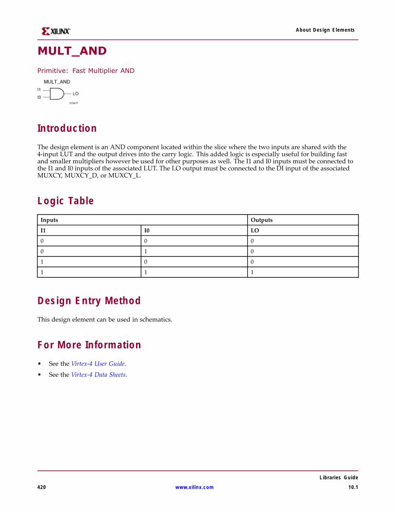
About Design Elements
MULT_AND
Primitive: Fast Multiplier AND
IntroductionThe design element is an AND component located within the slice where the two inputs are shared with the4-input LUT and the output drives into the carry logic. This added logic is especially useful for building fastand smaller multipliers however be used for other purposes as well. The I1 and I0 inputs must be connected tothe I1 and I0 inputs of the associated LUT. The LO output must be connected to the DI input of the associatedMUXCY, MUXCY_D, or MUXCY_L.
Logic TableInputs Outputs
I1 I0 LO
0 0 0
0 1 0
1 0 0
1 1 1
Design Entry MethodThis design element can be used in schematics.
For More Information• See the Virtex-4 User Guide.
• See the Virtex-4 Data Sheets.
Libraries Guide
420 www.xilinx.com 10.1
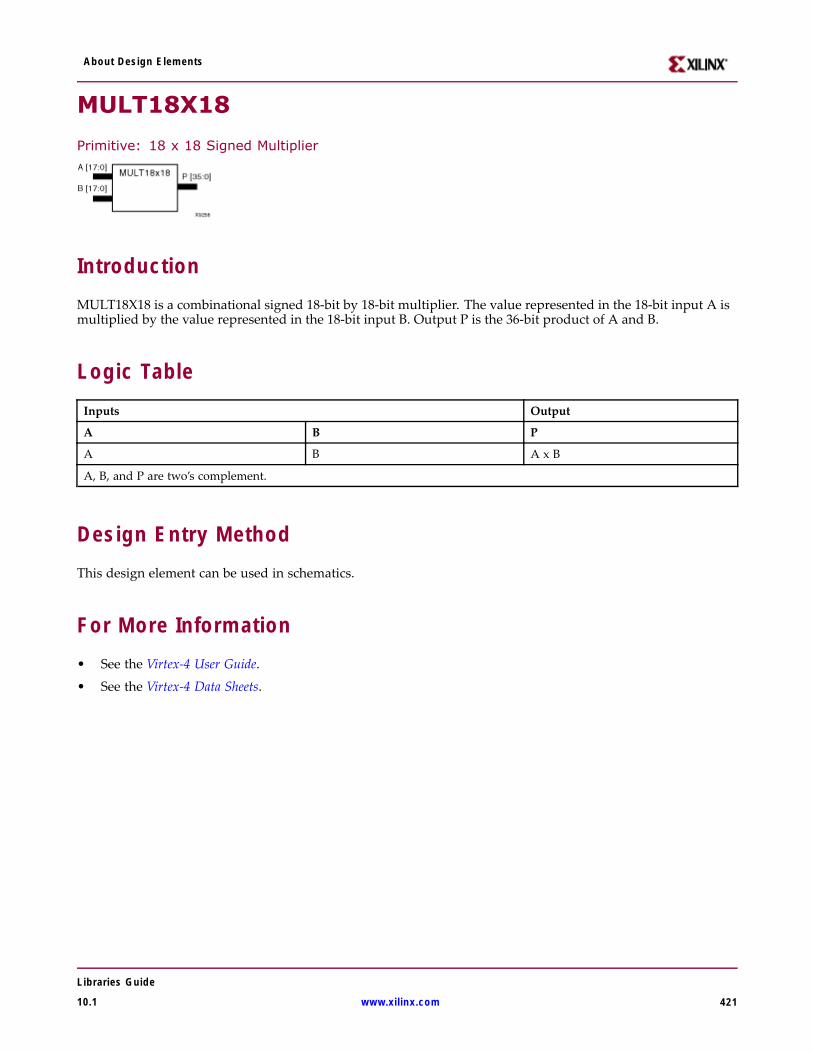
About Design Elements
MULT18X18
Primitive: 18 x 18 Signed Multiplier
IntroductionMULT18X18 is a combinational signed 18-bit by 18-bit multiplier. The value represented in the 18-bit input A ismultiplied by the value represented in the 18-bit input B. Output P is the 36-bit product of A and B.
Logic TableInputs Output
A B P
A B A x B
A, B, and P are two’s complement.
Design Entry MethodThis design element can be used in schematics.
For More Information• See the Virtex-4 User Guide.
• See the Virtex-4 Data Sheets.
Libraries Guide
10.1 www.xilinx.com 421
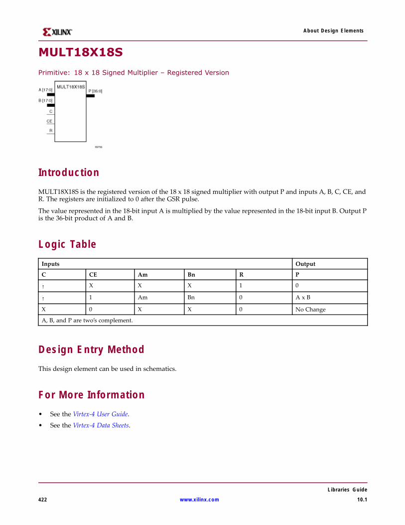
About Design Elements
MULT18X18S
Primitive: 18 x 18 Signed Multiplier – Registered Version
IntroductionMULT18X18S is the registered version of the 18 x 18 signed multiplier with output P and inputs A, B, C, CE, andR. The registers are initialized to 0 after the GSR pulse.
The value represented in the 18-bit input A is multiplied by the value represented in the 18-bit input B. Output Pis the 36-bit product of A and B.
Logic TableInputs Output
C CE Am Bn R P
↑ X X X 1 0
↑ 1 Am Bn 0 A x B
X 0 X X 0 No Change
A, B, and P are two’s complement.
Design Entry MethodThis design element can be used in schematics.
For More Information• See the Virtex-4 User Guide.
• See the Virtex-4 Data Sheets.
Libraries Guide
422 www.xilinx.com 10.1

About Design Elements
MUXCY
Primitive: 2-to-1 Multiplexer for Carry Logic with General Output
IntroductionThe direct input (DI) of a slice is connected to the (DI) input of the MUXCY. The carry in (CI) input of an LCis connected to the CI input of the MUXCY. The select input (S) of the MUXCY is driven by the output of theLook-Up Table (LUT) and configured as a MUX function. The carry out (O) of the MUXCY reflects the state of theselected input and implements the carry out function of each LC. When Low, S selects DI; when High, S selects CI.
The variants “MUXCY_D” and “MUXCY_L” provide additional types of outputs that can be used by differenttiming models for more accurate pre-layout timing estimation.
Logic TableInputs Outputs
S DI CI O
0 1 X 1
0 0 X 0
1 X 1 1
1 X 0 0
Design Entry MethodThis design element can be used in schematics.
For More Information• See the Virtex-4 User Guide.
• See the Virtex-4 Data Sheets.
Libraries Guide
10.1 www.xilinx.com 423
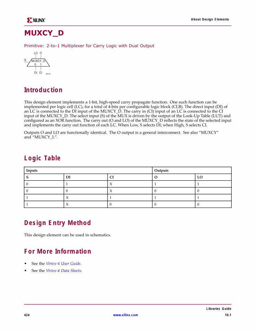
About Design Elements
MUXCY_D
Primitive: 2-to-1 Multiplexer for Carry Logic with Dual Output
IntroductionThis design element implements a 1-bit, high-speed carry propagate function. One such function can beimplemented per logic cell (LC), for a total of 4-bits per configurable logic block (CLB). The direct input (DI) ofan LC is connected to the DI input of the MUXCY_D. The carry in (CI) input of an LC is connected to the CIinput of the MUXCY_D. The select input (S) of the MUX is driven by the output of the Look-Up Table (LUT) andconfigured as an XOR function. The carry out (O and LO) of the MUXCY_D reflects the state of the selected inputand implements the carry out function of each LC. When Low, S selects DI; when High, S selects CI.
Outputs O and LO are functionally identical. The O output is a general interconnect. See also “MUXCY”and “MUXCY_L”.
Logic TableInputs Outputs
S DI CI O LO
0 1 X 1 1
0 0 X 0 0
1 X 1 1 1
1 X 0 0 0
Design Entry MethodThis design element can be used in schematics.
For More Information• See the Virtex-4 User Guide.
• See the Virtex-4 Data Sheets.
Libraries Guide
424 www.xilinx.com 10.1
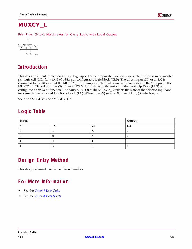
About Design Elements
MUXCY_L
Primitive: 2-to-1 Multiplexer for Carry Logic with Local Output
IntroductionThis design element implements a 1-bit high-speed carry propagate function. One such function is implementedper logic cell (LC), for a total of 4-bits per configurable logic block (CLB). The direct input (DI) of an LC isconnected to the DI input of the MUXCY_L. The carry in (CI) input of an LC is connected to the CI input of theMUXCY_L. The select input (S) of the MUXCY_L is driven by the output of the Look-Up Table (LUT) andconfigured as an XOR function. The carry out (LO) of the MUXCY_L reflects the state of the selected input andimplements the carry out function of each (LC). When Low, (S) selects DI; when High, (S) selects (CI).
See also “MUXCY” and “MUXCY_D.”
Logic TableInputs Outputs
S DI CI LO
0 1 X 1
0 0 X 0
1 X 1 1
1 X 0 0
Design Entry MethodThis design element can be used in schematics.
For More Information• See the Virtex-4 User Guide.
• See the Virtex-4 Data Sheets.
Libraries Guide
10.1 www.xilinx.com 425
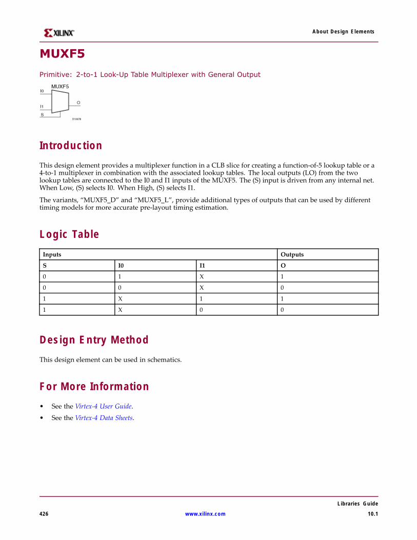
About Design Elements
MUXF5
Primitive: 2-to-1 Look-Up Table Multiplexer with General Output
IntroductionThis design element provides a multiplexer function in a CLB slice for creating a function-of-5 lookup table or a4-to-1 multiplexer in combination with the associated lookup tables. The local outputs (LO) from the twolookup tables are connected to the I0 and I1 inputs of the MUXF5. The (S) input is driven from any internal net.When Low, (S) selects I0. When High, (S) selects I1.
The variants, “MUXF5_D” and “MUXF5_L”, provide additional types of outputs that can be used by differenttiming models for more accurate pre-layout timing estimation.
Logic TableInputs Outputs
S I0 I1 O
0 1 X 1
0 0 X 0
1 X 1 1
1 X 0 0
Design Entry MethodThis design element can be used in schematics.
For More Information• See the Virtex-4 User Guide.
• See the Virtex-4 Data Sheets.
Libraries Guide
426 www.xilinx.com 10.1
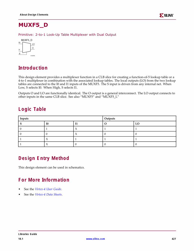
About Design Elements
MUXF5_D
Primitive: 2-to-1 Look-Up Table Multiplexer with Dual Output
IntroductionThis design element provides a multiplexer function in a CLB slice for creating a function-of-5 lookup table or a4-to-1 multiplexer in combination with the associated lookup tables. The local outputs (LO) from the two lookuptables are connected to the I0 and I1 inputs of the MUXF5. The S input is driven from any internal net. WhenLow, S selects I0. When High, S selects I1.
Outputs O and LO are functionally identical. The O output is a general interconnect. The LO output connects toother inputs in the same CLB slice. See also “MUXF5” and “MUXF5_L”
Logic TableInputs Outputs
S I0 I1 O LO
0 1 X 1 1
0 0 X 0 0
1 X 1 1 1
1 X 0 0 0
Design Entry MethodThis design element can be used in schematics.
For More Information• See the Virtex-4 User Guide.
• See the Virtex-4 Data Sheets.
Libraries Guide
10.1 www.xilinx.com 427
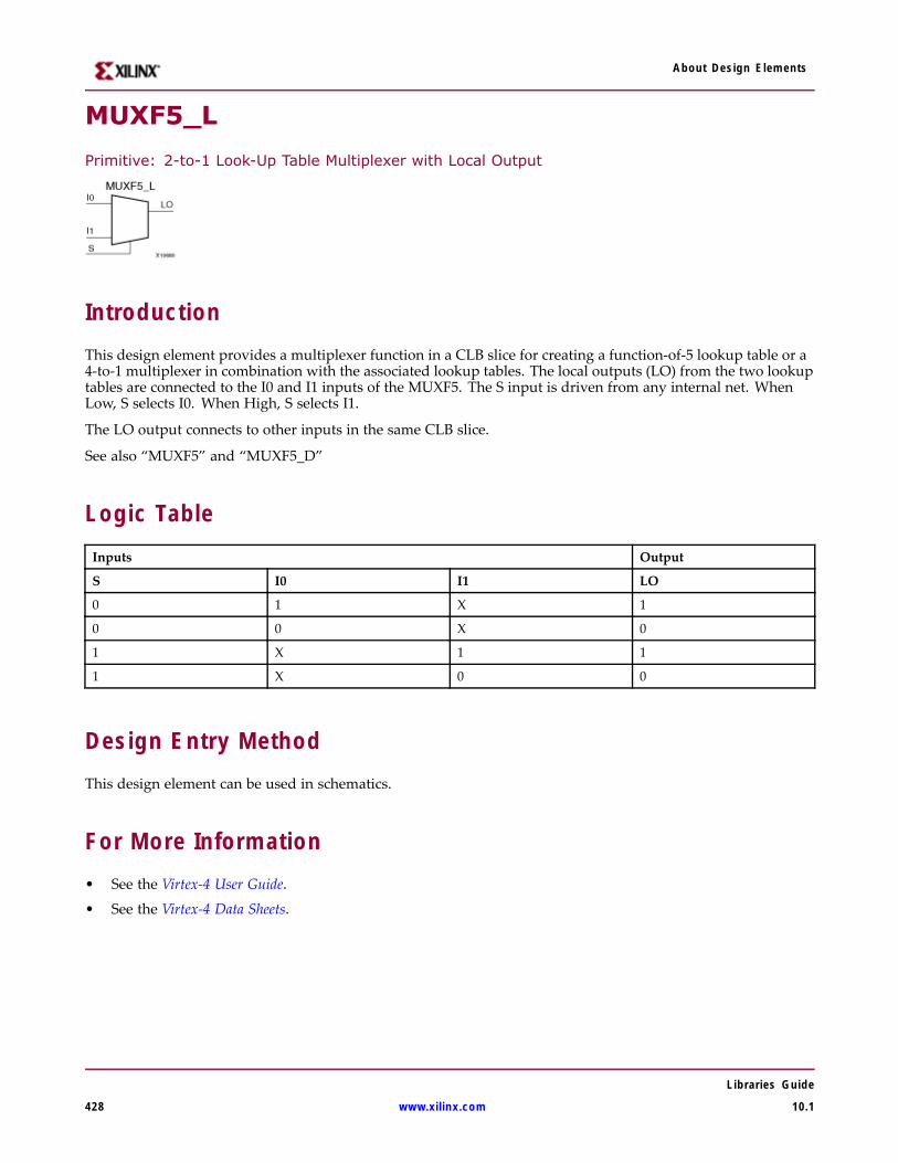
About Design Elements
MUXF5_L
Primitive: 2-to-1 Look-Up Table Multiplexer with Local Output
IntroductionThis design element provides a multiplexer function in a CLB slice for creating a function-of-5 lookup table or a4-to-1 multiplexer in combination with the associated lookup tables. The local outputs (LO) from the two lookuptables are connected to the I0 and I1 inputs of the MUXF5. The S input is driven from any internal net. WhenLow, S selects I0. When High, S selects I1.
The LO output connects to other inputs in the same CLB slice.
See also “MUXF5” and “MUXF5_D”
Logic TableInputs Output
S I0 I1 LO
0 1 X 1
0 0 X 0
1 X 1 1
1 X 0 0
Design Entry MethodThis design element can be used in schematics.
For More Information• See the Virtex-4 User Guide.
• See the Virtex-4 Data Sheets.
Libraries Guide
428 www.xilinx.com 10.1
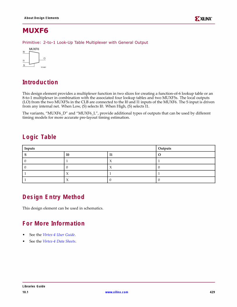
About Design Elements
MUXF6
Primitive: 2-to-1 Look-Up Table Multiplexer with General Output
IntroductionThis design element provides a multiplexer function in two slices for creating a function-of-6 lookup table or an8-to-1 multiplexer in combination with the associated four lookup tables and two MUXF5s. The local outputs(LO) from the two MUXF5s in the CLB are connected to the I0 and I1 inputs of the MUXF6. The S input is drivenfrom any internal net. When Low, (S) selects I0. When High, (S) selects I1.
The variants, “MUXF6_D” and “MUXF6_L”, provide additional types of outputs that can be used by differenttiming models for more accurate pre-layout timing estimation.
Logic TableInputs Outputs
S I0 I1 O
0 1 X 1
0 0 X 0
1 X 1 1
1 X 0 0
Design Entry MethodThis design element can be used in schematics.
For More Information• See the Virtex-4 User Guide.
• See the Virtex-4 Data Sheets.
Libraries Guide
10.1 www.xilinx.com 429
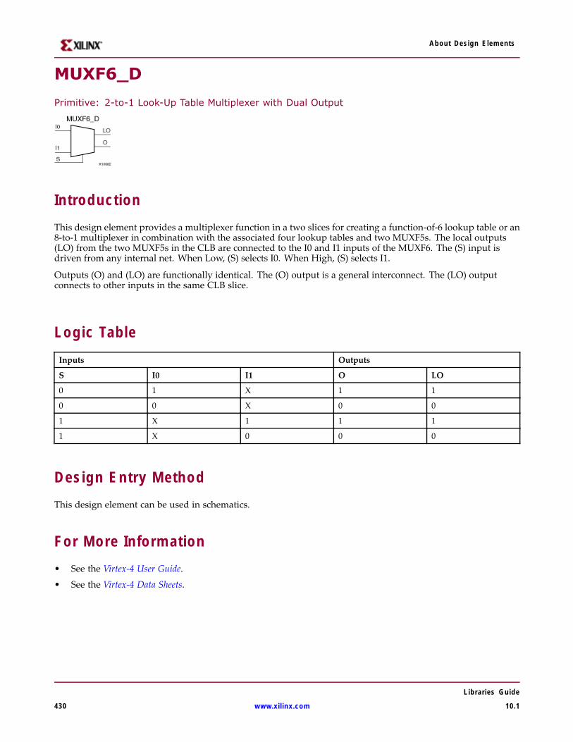
About Design Elements
MUXF6_D
Primitive: 2-to-1 Look-Up Table Multiplexer with Dual Output
IntroductionThis design element provides a multiplexer function in a two slices for creating a function-of-6 lookup table or an8-to-1 multiplexer in combination with the associated four lookup tables and two MUXF5s. The local outputs(LO) from the two MUXF5s in the CLB are connected to the I0 and I1 inputs of the MUXF6. The (S) input isdriven from any internal net. When Low, (S) selects I0. When High, (S) selects I1.
Outputs (O) and (LO) are functionally identical. The (O) output is a general interconnect. The (LO) outputconnects to other inputs in the same CLB slice.
Logic TableInputs Outputs
S I0 I1 O LO
0 1 X 1 1
0 0 X 0 0
1 X 1 1 1
1 X 0 0 0
Design Entry MethodThis design element can be used in schematics.
For More Information• See the Virtex-4 User Guide.
• See the Virtex-4 Data Sheets.
Libraries Guide
430 www.xilinx.com 10.1
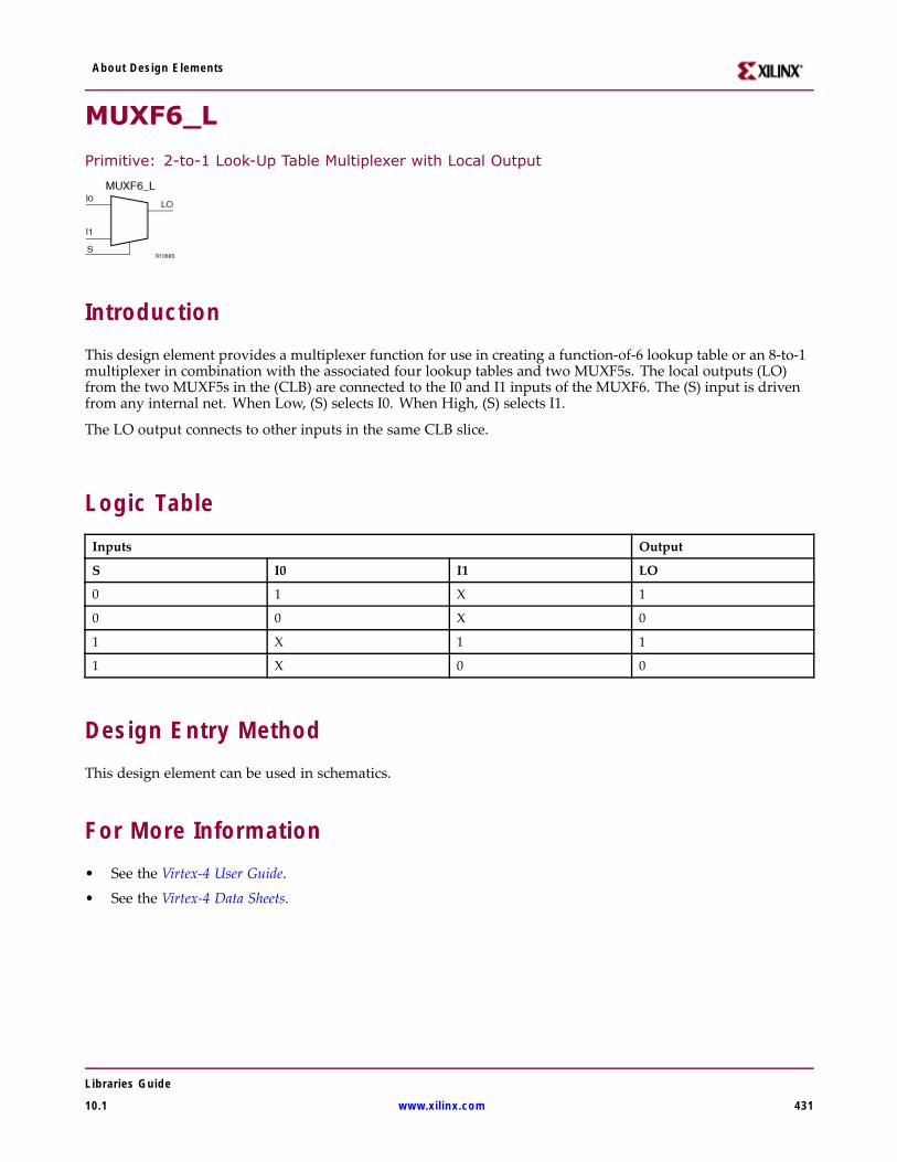
About Design Elements
MUXF6_L
Primitive: 2-to-1 Look-Up Table Multiplexer with Local Output
IntroductionThis design element provides a multiplexer function for use in creating a function-of-6 lookup table or an 8-to-1multiplexer in combination with the associated four lookup tables and two MUXF5s. The local outputs (LO)from the two MUXF5s in the (CLB) are connected to the I0 and I1 inputs of the MUXF6. The (S) input is drivenfrom any internal net. When Low, (S) selects I0. When High, (S) selects I1.
The LO output connects to other inputs in the same CLB slice.
Logic TableInputs Output
S I0 I1 LO
0 1 X 1
0 0 X 0
1 X 1 1
1 X 0 0
Design Entry MethodThis design element can be used in schematics.
For More Information• See the Virtex-4 User Guide.
• See the Virtex-4 Data Sheets.
Libraries Guide
10.1 www.xilinx.com 431
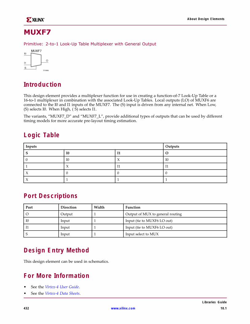
About Design Elements
MUXF7
Primitive: 2-to-1 Look-Up Table Multiplexer with General Output
IntroductionThis design element provides a multiplexer function for use in creating a function-of-7 Look-Up Table or a16-to-1 multiplexer in combination with the associated Look-Up Tables. Local outputs (LO) of MUXF6 areconnected to the I0 and I1 inputs of the MUXF7. The (S) input is driven from any internal net. When Low,(S) selects I0. When High, ( S) selects I1.
The variants, “MUXF7_D” and “MUXF7_L”, provide additional types of outputs that can be used by differenttiming models for more accurate pre-layout timing estimation.
Logic TableInputs Outputs
S I0 I1 O
0 I0 X I0
1 X I1 I1
X 0 0 0
X 1 1 1
Port DescriptionsPort Direction Width Function
O Output 1 Output of MUX to general routing
I0 Input 1 Input (tie to MUXF6 LO out)
I1 Input 1 Input (tie to MUXF6 LO out)
S Input 1 Input select to MUX
Design Entry MethodThis design element can be used in schematics.
For More Information• See the Virtex-4 User Guide.• See the Virtex-4 Data Sheets.
Libraries Guide
432 www.xilinx.com 10.1
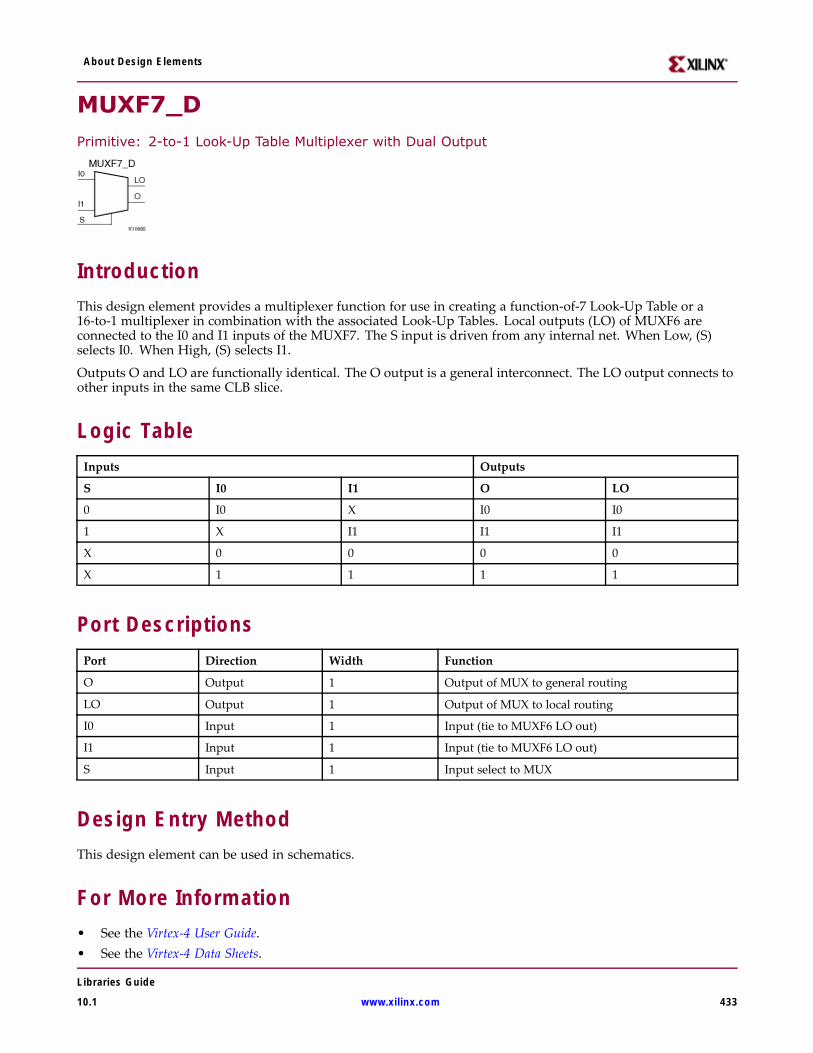
About Design Elements
MUXF7_DPrimitive: 2-to-1 Look-Up Table Multiplexer with Dual Output
IntroductionThis design element provides a multiplexer function for use in creating a function-of-7 Look-Up Table or a16-to-1 multiplexer in combination with the associated Look-Up Tables. Local outputs (LO) of MUXF6 areconnected to the I0 and I1 inputs of the MUXF7. The S input is driven from any internal net. When Low, (S)selects I0. When High, (S) selects I1.
Outputs O and LO are functionally identical. The O output is a general interconnect. The LO output connects toother inputs in the same CLB slice.
Logic TableInputs Outputs
S I0 I1 O LO
0 I0 X I0 I0
1 X I1 I1 I1
X 0 0 0 0
X 1 1 1 1
Port DescriptionsPort Direction Width Function
O Output 1 Output of MUX to general routing
LO Output 1 Output of MUX to local routing
I0 Input 1 Input (tie to MUXF6 LO out)
I1 Input 1 Input (tie to MUXF6 LO out)
S Input 1 Input select to MUX
Design Entry MethodThis design element can be used in schematics.
For More Information• See the Virtex-4 User Guide.• See the Virtex-4 Data Sheets.
Libraries Guide
10.1 www.xilinx.com 433
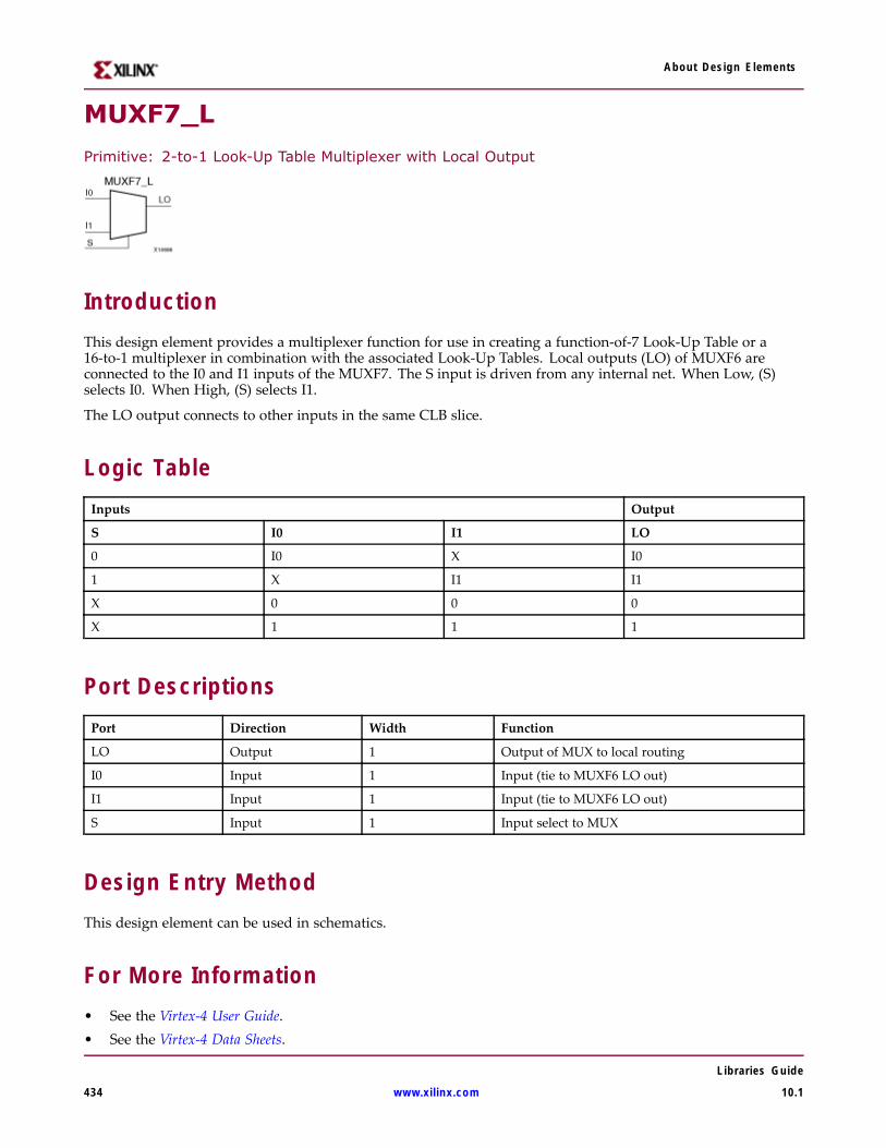
About Design Elements
MUXF7_L
Primitive: 2-to-1 Look-Up Table Multiplexer with Local Output
IntroductionThis design element provides a multiplexer function for use in creating a function-of-7 Look-Up Table or a16-to-1 multiplexer in combination with the associated Look-Up Tables. Local outputs (LO) of MUXF6 areconnected to the I0 and I1 inputs of the MUXF7. The S input is driven from any internal net. When Low, (S)selects I0. When High, (S) selects I1.
The LO output connects to other inputs in the same CLB slice.
Logic TableInputs Output
S I0 I1 LO
0 I0 X I0
1 X I1 I1
X 0 0 0
X 1 1 1
Port DescriptionsPort Direction Width Function
LO Output 1 Output of MUX to local routing
I0 Input 1 Input (tie to MUXF6 LO out)
I1 Input 1 Input (tie to MUXF6 LO out)
S Input 1 Input select to MUX
Design Entry MethodThis design element can be used in schematics.
For More Information• See the Virtex-4 User Guide.• See the Virtex-4 Data Sheets.
Libraries Guide
434 www.xilinx.com 10.1
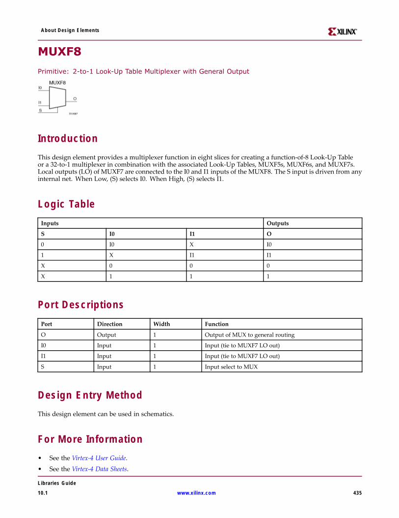
About Design Elements
MUXF8
Primitive: 2-to-1 Look-Up Table Multiplexer with General Output
IntroductionThis design element provides a multiplexer function in eight slices for creating a function-of-8 Look-Up Tableor a 32-to-1 multiplexer in combination with the associated Look-Up Tables, MUXF5s, MUXF6s, and MUXF7s.Local outputs (LO) of MUXF7 are connected to the I0 and I1 inputs of the MUXF8. The S input is driven from anyinternal net. When Low, (S) selects I0. When High, (S) selects I1.
Logic TableInputs Outputs
S I0 I1 O
0 I0 X I0
1 X I1 I1
X 0 0 0
X 1 1 1
Port DescriptionsPort Direction Width Function
O Output 1 Output of MUX to general routing
I0 Input 1 Input (tie to MUXF7 LO out)
I1 Input 1 Input (tie to MUXF7 LO out)
S Input 1 Input select to MUX
Design Entry MethodThis design element can be used in schematics.
For More Information• See the Virtex-4 User Guide.
• See the Virtex-4 Data Sheets.
Libraries Guide
10.1 www.xilinx.com 435
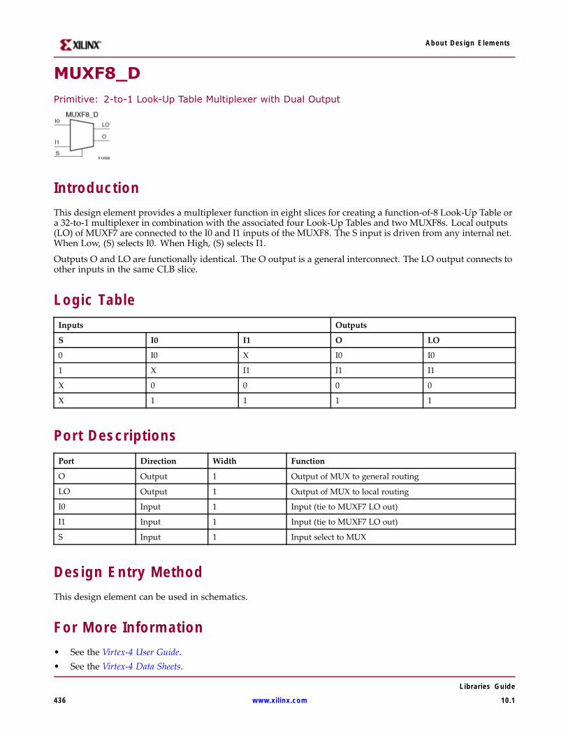
About Design Elements
MUXF8_DPrimitive: 2-to-1 Look-Up Table Multiplexer with Dual Output
IntroductionThis design element provides a multiplexer function in eight slices for creating a function-of-8 Look-Up Table ora 32-to-1 multiplexer in combination with the associated four Look-Up Tables and two MUXF8s. Local outputs(LO) of MUXF7 are connected to the I0 and I1 inputs of the MUXF8. The S input is driven from any internal net.When Low, (S) selects I0. When High, (S) selects I1.
Outputs O and LO are functionally identical. The O output is a general interconnect. The LO output connects toother inputs in the same CLB slice.
Logic TableInputs Outputs
S I0 I1 O LO
0 I0 X I0 I0
1 X I1 I1 I1
X 0 0 0 0
X 1 1 1 1
Port DescriptionsPort Direction Width Function
O Output 1 Output of MUX to general routing
LO Output 1 Output of MUX to local routing
I0 Input 1 Input (tie to MUXF7 LO out)
I1 Input 1 Input (tie to MUXF7 LO out)
S Input 1 Input select to MUX
Design Entry MethodThis design element can be used in schematics.
For More Information• See the Virtex-4 User Guide.• See the Virtex-4 Data Sheets.
Libraries Guide
436 www.xilinx.com 10.1
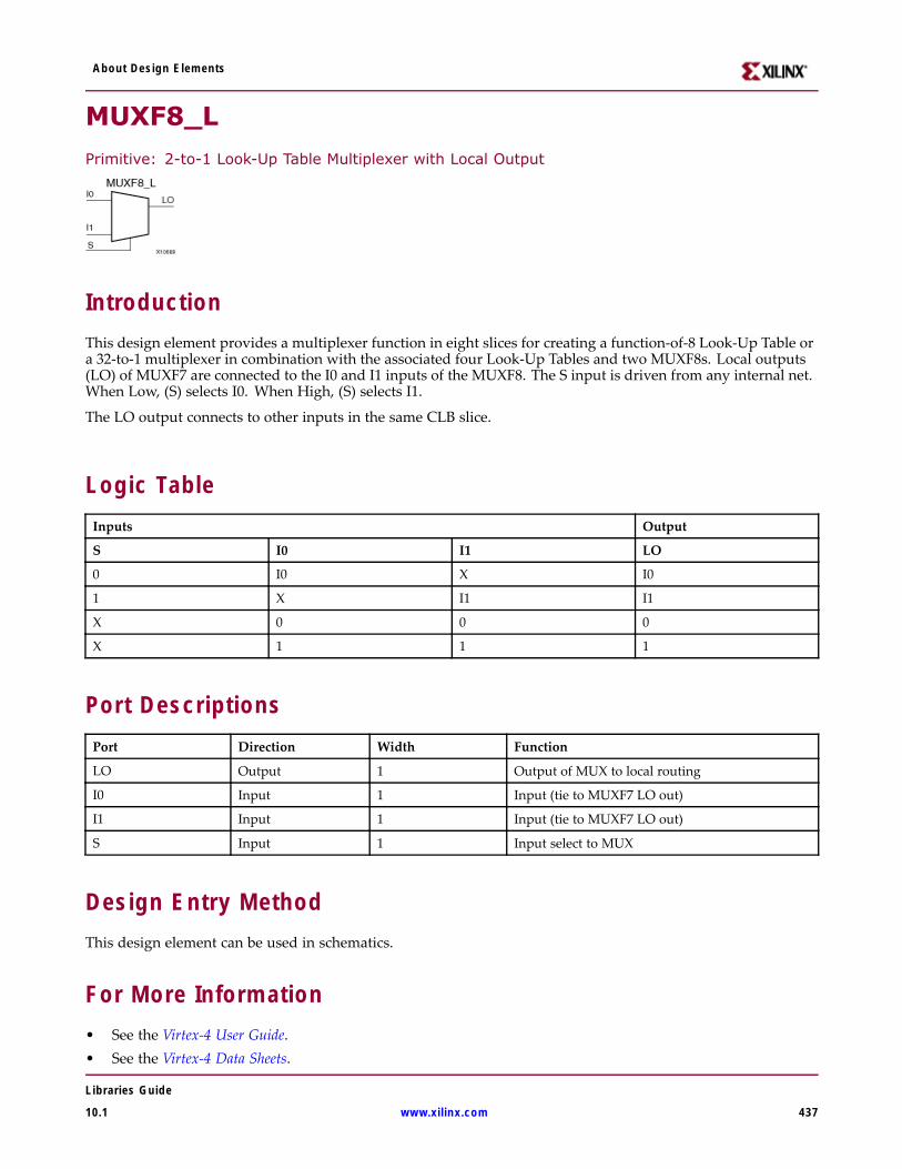
About Design Elements
MUXF8_L
Primitive: 2-to-1 Look-Up Table Multiplexer with Local Output
IntroductionThis design element provides a multiplexer function in eight slices for creating a function-of-8 Look-Up Table ora 32-to-1 multiplexer in combination with the associated four Look-Up Tables and two MUXF8s. Local outputs(LO) of MUXF7 are connected to the I0 and I1 inputs of the MUXF8. The S input is driven from any internal net.When Low, (S) selects I0. When High, (S) selects I1.
The LO output connects to other inputs in the same CLB slice.
Logic TableInputs Output
S I0 I1 LO
0 I0 X I0
1 X I1 I1
X 0 0 0
X 1 1 1
Port DescriptionsPort Direction Width Function
LO Output 1 Output of MUX to local routing
I0 Input 1 Input (tie to MUXF7 LO out)
I1 Input 1 Input (tie to MUXF7 LO out)
S Input 1 Input select to MUX
Design Entry MethodThis design element can be used in schematics.
For More Information• See the Virtex-4 User Guide.• See the Virtex-4 Data Sheets.
Libraries Guide
10.1 www.xilinx.com 437
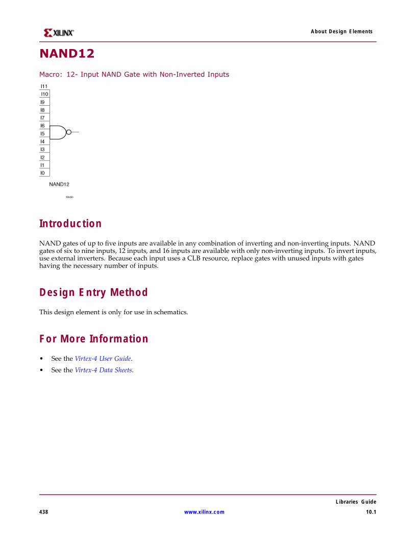
About Design Elements
NAND12
Macro: 12- Input NAND Gate with Non-Inverted Inputs
IntroductionNAND gates of up to five inputs are available in any combination of inverting and non-inverting inputs. NANDgates of six to nine inputs, 12 inputs, and 16 inputs are available with only non-inverting inputs. To invert inputs,use external inverters. Because each input uses a CLB resource, replace gates with unused inputs with gateshaving the necessary number of inputs.
Design Entry MethodThis design element is only for use in schematics.
For More Information• See the Virtex-4 User Guide.
• See the Virtex-4 Data Sheets.
Libraries Guide
438 www.xilinx.com 10.1
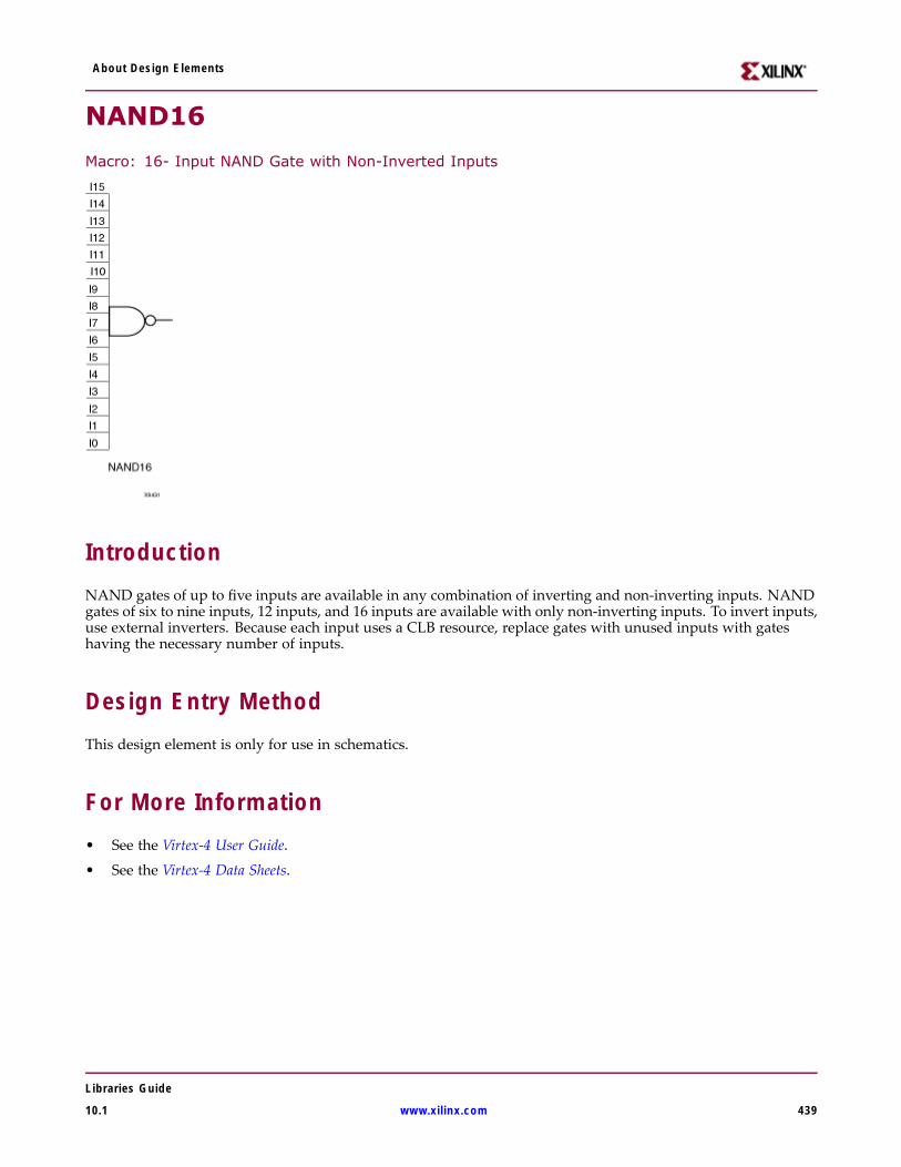
About Design Elements
NAND16
Macro: 16- Input NAND Gate with Non-Inverted Inputs
IntroductionNAND gates of up to five inputs are available in any combination of inverting and non-inverting inputs. NANDgates of six to nine inputs, 12 inputs, and 16 inputs are available with only non-inverting inputs. To invert inputs,use external inverters. Because each input uses a CLB resource, replace gates with unused inputs with gateshaving the necessary number of inputs.
Design Entry MethodThis design element is only for use in schematics.
For More Information• See the Virtex-4 User Guide.
• See the Virtex-4 Data Sheets.
Libraries Guide
10.1 www.xilinx.com 439
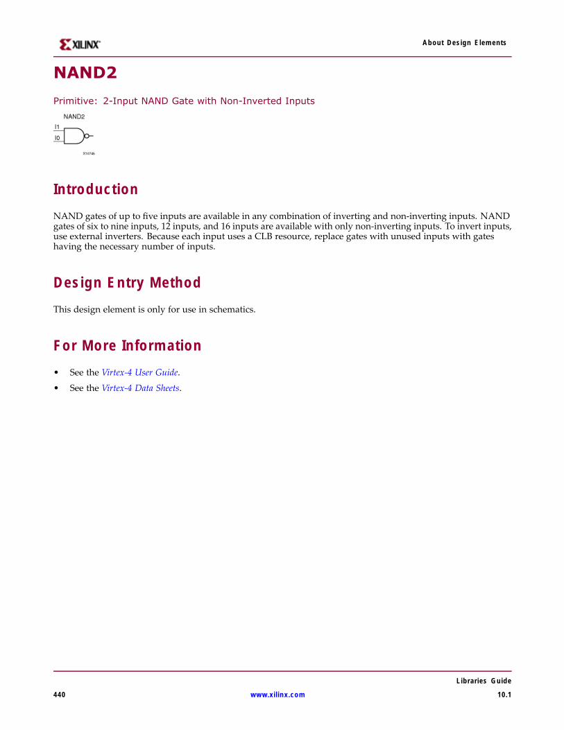
About Design Elements
NAND2
Primitive: 2-Input NAND Gate with Non-Inverted Inputs
IntroductionNAND gates of up to five inputs are available in any combination of inverting and non-inverting inputs. NANDgates of six to nine inputs, 12 inputs, and 16 inputs are available with only non-inverting inputs. To invert inputs,use external inverters. Because each input uses a CLB resource, replace gates with unused inputs with gateshaving the necessary number of inputs.
Design Entry MethodThis design element is only for use in schematics.
For More Information• See the Virtex-4 User Guide.
• See the Virtex-4 Data Sheets.
Libraries Guide
440 www.xilinx.com 10.1
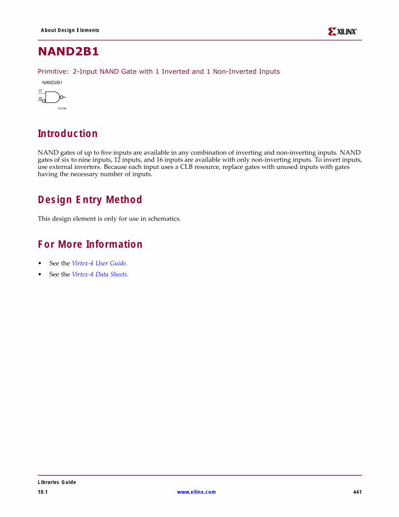
About Design Elements
NAND2B1
Primitive: 2-Input NAND Gate with 1 Inverted and 1 Non-Inverted Inputs
IntroductionNAND gates of up to five inputs are available in any combination of inverting and non-inverting inputs. NANDgates of six to nine inputs, 12 inputs, and 16 inputs are available with only non-inverting inputs. To invert inputs,use external inverters. Because each input uses a CLB resource, replace gates with unused inputs with gateshaving the necessary number of inputs.
Design Entry MethodThis design element is only for use in schematics.
For More Information• See the Virtex-4 User Guide.
• See the Virtex-4 Data Sheets.
Libraries Guide
10.1 www.xilinx.com 441

About Design Elements
NAND2B2
Primitive: 2-Input NAND Gate with Inverted Inputs
IntroductionNAND gates of up to five inputs are available in any combination of inverting and non-inverting inputs. NANDgates of six to nine inputs, 12 inputs, and 16 inputs are available with only non-inverting inputs. To invert inputs,use external inverters. Because each input uses a CLB resource, replace gates with unused inputs with gateshaving the necessary number of inputs.
Design Entry MethodThis design element is only for use in schematics.
For More Information• See the Virtex-4 User Guide.
• See the Virtex-4 Data Sheets.
Libraries Guide
442 www.xilinx.com 10.1

About Design Elements
NAND3
Primitive: 3-Input NAND Gate with Non-Inverted Inputs
IntroductionNAND gates of up to five inputs are available in any combination of inverting and non-inverting inputs. NANDgates of six to nine inputs, 12 inputs, and 16 inputs are available with only non-inverting inputs. To invert inputs,use external inverters. Because each input uses a CLB resource, replace gates with unused inputs with gateshaving the necessary number of inputs.
Design Entry MethodThis design element is only for use in schematics.
For More Information• See the Virtex-4 User Guide.
• See the Virtex-4 Data Sheets.
Libraries Guide
10.1 www.xilinx.com 443
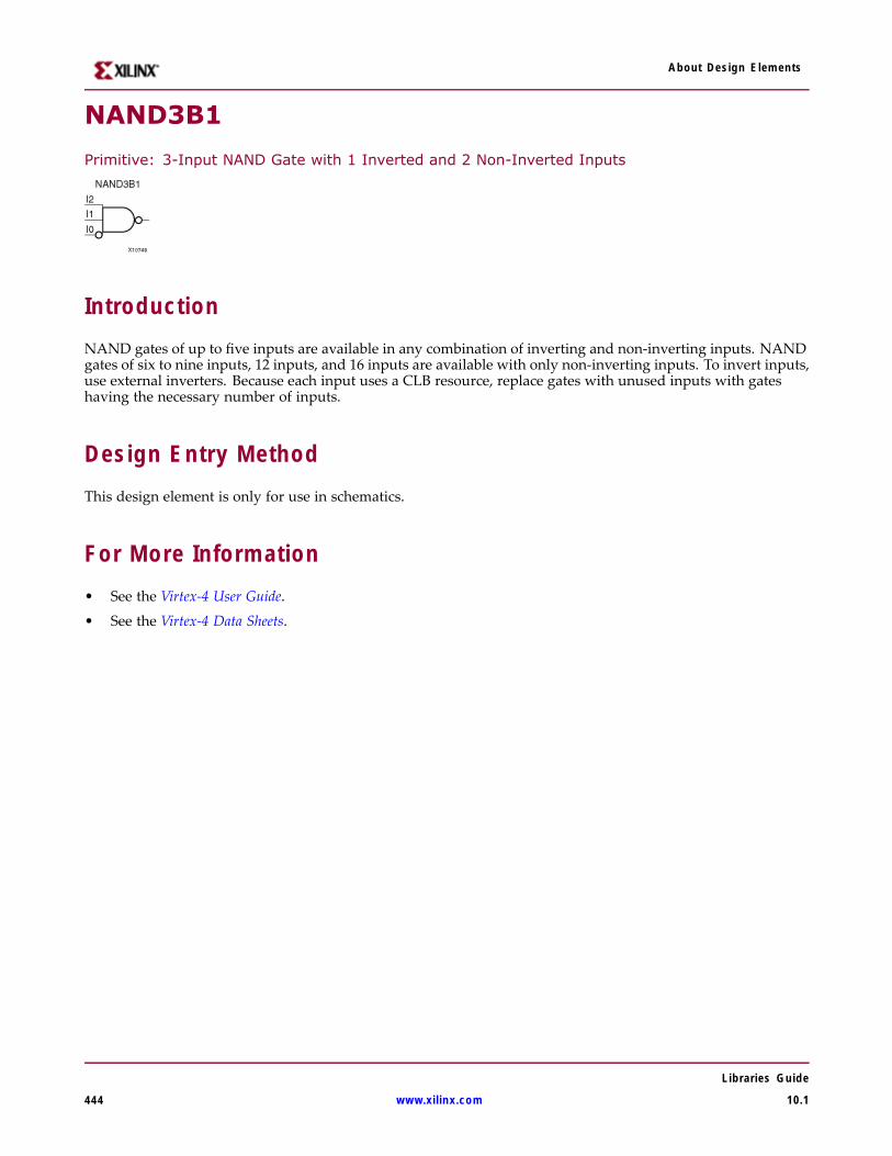
About Design Elements
NAND3B1
Primitive: 3-Input NAND Gate with 1 Inverted and 2 Non-Inverted Inputs
IntroductionNAND gates of up to five inputs are available in any combination of inverting and non-inverting inputs. NANDgates of six to nine inputs, 12 inputs, and 16 inputs are available with only non-inverting inputs. To invert inputs,use external inverters. Because each input uses a CLB resource, replace gates with unused inputs with gateshaving the necessary number of inputs.
Design Entry MethodThis design element is only for use in schematics.
For More Information• See the Virtex-4 User Guide.
• See the Virtex-4 Data Sheets.
Libraries Guide
444 www.xilinx.com 10.1

About Design Elements
NAND3B2
Primitive: 3-Input NAND Gate with 2 Inverted and 1 Non-Inverted Inputs
IntroductionNAND gates of up to five inputs are available in any combination of inverting and non-inverting inputs. NANDgates of six to nine inputs, 12 inputs, and 16 inputs are available with only non-inverting inputs. To invert inputs,use external inverters. Because each input uses a CLB resource, replace gates with unused inputs with gateshaving the necessary number of inputs.
Design Entry MethodThis design element is only for use in schematics.
For More Information• See the Virtex-4 User Guide.
• See the Virtex-4 Data Sheets.
Libraries Guide
10.1 www.xilinx.com 445
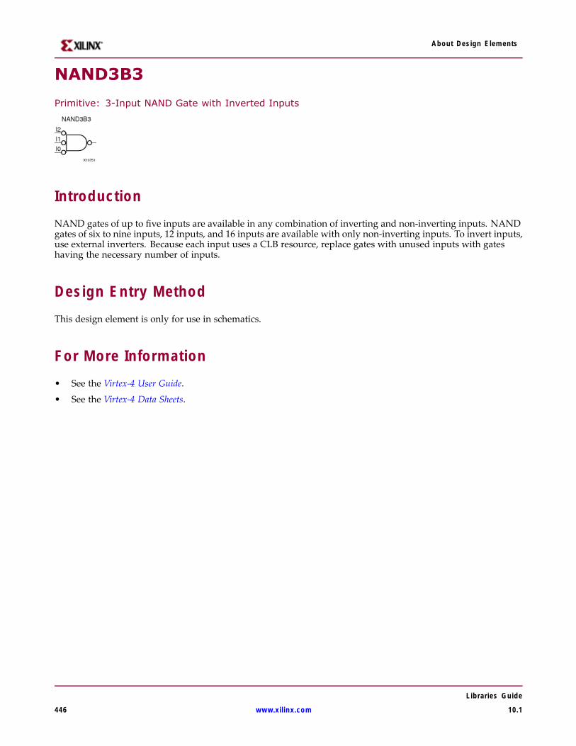
About Design Elements
NAND3B3
Primitive: 3-Input NAND Gate with Inverted Inputs
IntroductionNAND gates of up to five inputs are available in any combination of inverting and non-inverting inputs. NANDgates of six to nine inputs, 12 inputs, and 16 inputs are available with only non-inverting inputs. To invert inputs,use external inverters. Because each input uses a CLB resource, replace gates with unused inputs with gateshaving the necessary number of inputs.
Design Entry MethodThis design element is only for use in schematics.
For More Information• See the Virtex-4 User Guide.
• See the Virtex-4 Data Sheets.
Libraries Guide
446 www.xilinx.com 10.1

About Design Elements
NAND4
Primitive: 4-Input NAND Gate with Non-Inverted Inputs
IntroductionNAND gates of up to five inputs are available in any combination of inverting and non-inverting inputs. NANDgates of six to nine inputs, 12 inputs, and 16 inputs are available with only non-inverting inputs. To invert inputs,use external inverters. Because each input uses a CLB resource, replace gates with unused inputs with gateshaving the necessary number of inputs.
Design Entry MethodThis design element is only for use in schematics.
For More Information• See the Virtex-4 User Guide.
• See the Virtex-4 Data Sheets.
Libraries Guide
10.1 www.xilinx.com 447

About Design Elements
NAND4B1
Primitive: 4-Input NAND Gate with 1 Inverted and 3 Non-Inverted Inputs
IntroductionNAND gates of up to five inputs are available in any combination of inverting and non-inverting inputs. NANDgates of six to nine inputs, 12 inputs, and 16 inputs are available with only non-inverting inputs. To invert inputs,use external inverters. Because each input uses a CLB resource, replace gates with unused inputs with gateshaving the necessary number of inputs.
Design Entry MethodThis design element is only for use in schematics.
For More Information• See the Virtex-4 User Guide.
• See the Virtex-4 Data Sheets.
Libraries Guide
448 www.xilinx.com 10.1
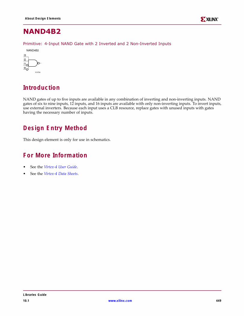
About Design Elements
NAND4B2
Primitive: 4-Input NAND Gate with 2 Inverted and 2 Non-Inverted Inputs
IntroductionNAND gates of up to five inputs are available in any combination of inverting and non-inverting inputs. NANDgates of six to nine inputs, 12 inputs, and 16 inputs are available with only non-inverting inputs. To invert inputs,use external inverters. Because each input uses a CLB resource, replace gates with unused inputs with gateshaving the necessary number of inputs.
Design Entry MethodThis design element is only for use in schematics.
For More Information• See the Virtex-4 User Guide.
• See the Virtex-4 Data Sheets.
Libraries Guide
10.1 www.xilinx.com 449
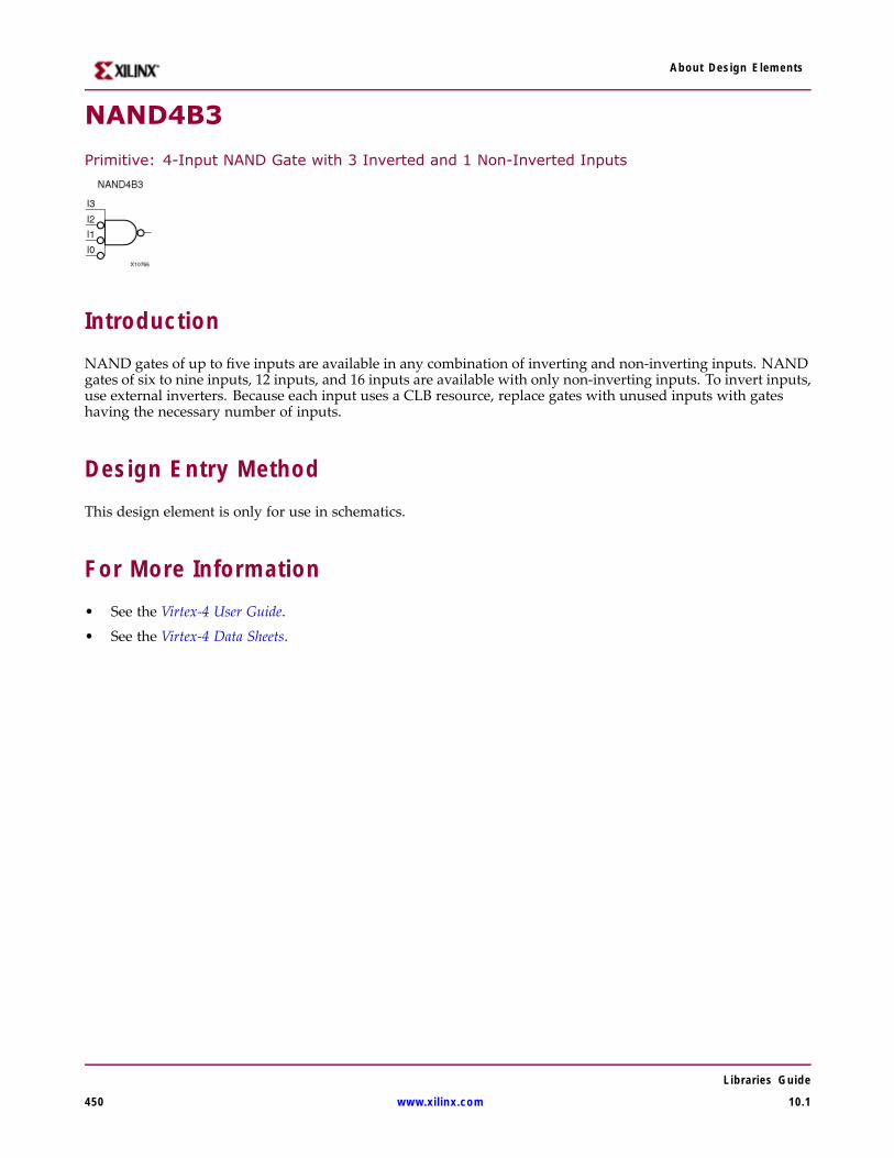
About Design Elements
NAND4B3
Primitive: 4-Input NAND Gate with 3 Inverted and 1 Non-Inverted Inputs
IntroductionNAND gates of up to five inputs are available in any combination of inverting and non-inverting inputs. NANDgates of six to nine inputs, 12 inputs, and 16 inputs are available with only non-inverting inputs. To invert inputs,use external inverters. Because each input uses a CLB resource, replace gates with unused inputs with gateshaving the necessary number of inputs.
Design Entry MethodThis design element is only for use in schematics.
For More Information• See the Virtex-4 User Guide.
• See the Virtex-4 Data Sheets.
Libraries Guide
450 www.xilinx.com 10.1

About Design Elements
NAND4B4
Primitive: 4-Input NAND Gate with Inverted Inputs
IntroductionNAND gates of up to five inputs are available in any combination of inverting and non-inverting inputs. NANDgates of six to nine inputs, 12 inputs, and 16 inputs are available with only non-inverting inputs. To invert inputs,use external inverters. Because each input uses a CLB resource, replace gates with unused inputs with gateshaving the necessary number of inputs.
Design Entry MethodThis design element is only for use in schematics.
For More Information• See the Virtex-4 User Guide.
• See the Virtex-4 Data Sheets.
Libraries Guide
10.1 www.xilinx.com 451
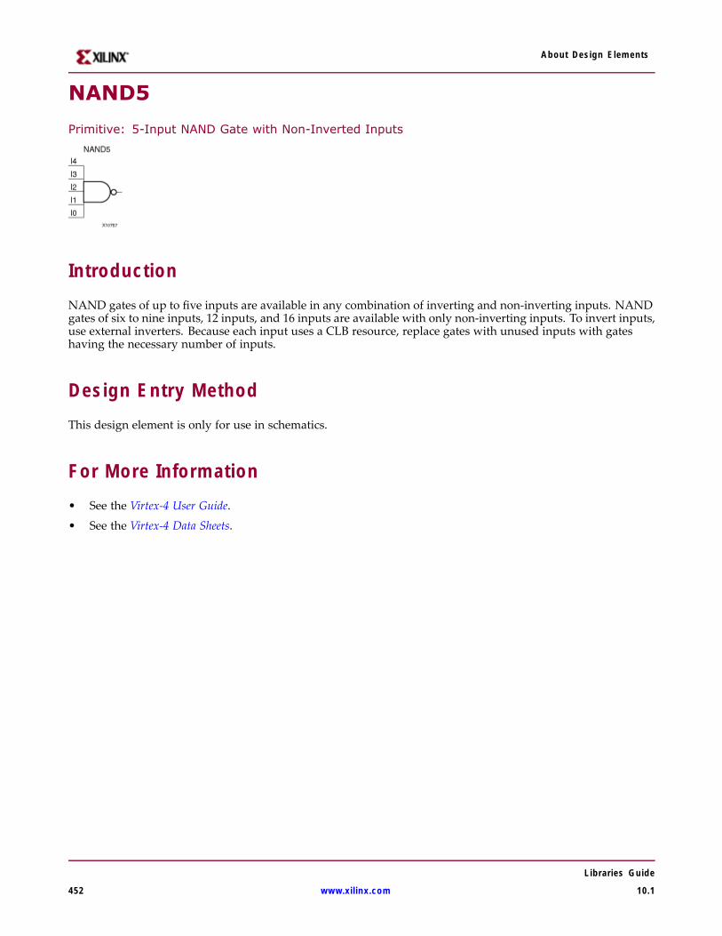
About Design Elements
NAND5
Primitive: 5-Input NAND Gate with Non-Inverted Inputs
IntroductionNAND gates of up to five inputs are available in any combination of inverting and non-inverting inputs. NANDgates of six to nine inputs, 12 inputs, and 16 inputs are available with only non-inverting inputs. To invert inputs,use external inverters. Because each input uses a CLB resource, replace gates with unused inputs with gateshaving the necessary number of inputs.
Design Entry MethodThis design element is only for use in schematics.
For More Information• See the Virtex-4 User Guide.
• See the Virtex-4 Data Sheets.
Libraries Guide
452 www.xilinx.com 10.1

About Design Elements
NAND5B1
Primitive: 5-Input NAND Gate with 1 Inverted and 4 Non-Inverted Inputs
IntroductionNAND gates of up to five inputs are available in any combination of inverting and non-inverting inputs. NANDgates of six to nine inputs, 12 inputs, and 16 inputs are available with only non-inverting inputs. To invert inputs,use external inverters. Because each input uses a CLB resource, replace gates with unused inputs with gateshaving the necessary number of inputs.
Design Entry MethodThis design element is only for use in schematics.
For More Information• See the Virtex-4 User Guide.
• See the Virtex-4 Data Sheets.
Libraries Guide
10.1 www.xilinx.com 453
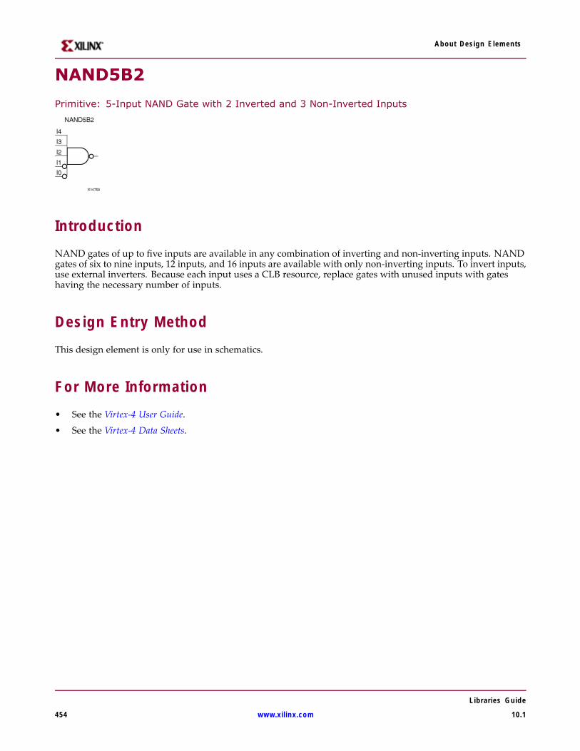
About Design Elements
NAND5B2
Primitive: 5-Input NAND Gate with 2 Inverted and 3 Non-Inverted Inputs
IntroductionNAND gates of up to five inputs are available in any combination of inverting and non-inverting inputs. NANDgates of six to nine inputs, 12 inputs, and 16 inputs are available with only non-inverting inputs. To invert inputs,use external inverters. Because each input uses a CLB resource, replace gates with unused inputs with gateshaving the necessary number of inputs.
Design Entry MethodThis design element is only for use in schematics.
For More Information• See the Virtex-4 User Guide.
• See the Virtex-4 Data Sheets.
Libraries Guide
454 www.xilinx.com 10.1

About Design Elements
NAND5B3
Primitive: 5-Input NAND Gate with 3 Inverted and 2 Non-Inverted Inputs
IntroductionNAND gates of up to five inputs are available in any combination of inverting and non-inverting inputs. NANDgates of six to nine inputs, 12 inputs, and 16 inputs are available with only non-inverting inputs. To invert inputs,use external inverters. Because each input uses a CLB resource, replace gates with unused inputs with gateshaving the necessary number of inputs.
Design Entry MethodThis design element is only for use in schematics.
For More Information• See the Virtex-4 User Guide.
• See the Virtex-4 Data Sheets.
Libraries Guide
10.1 www.xilinx.com 455
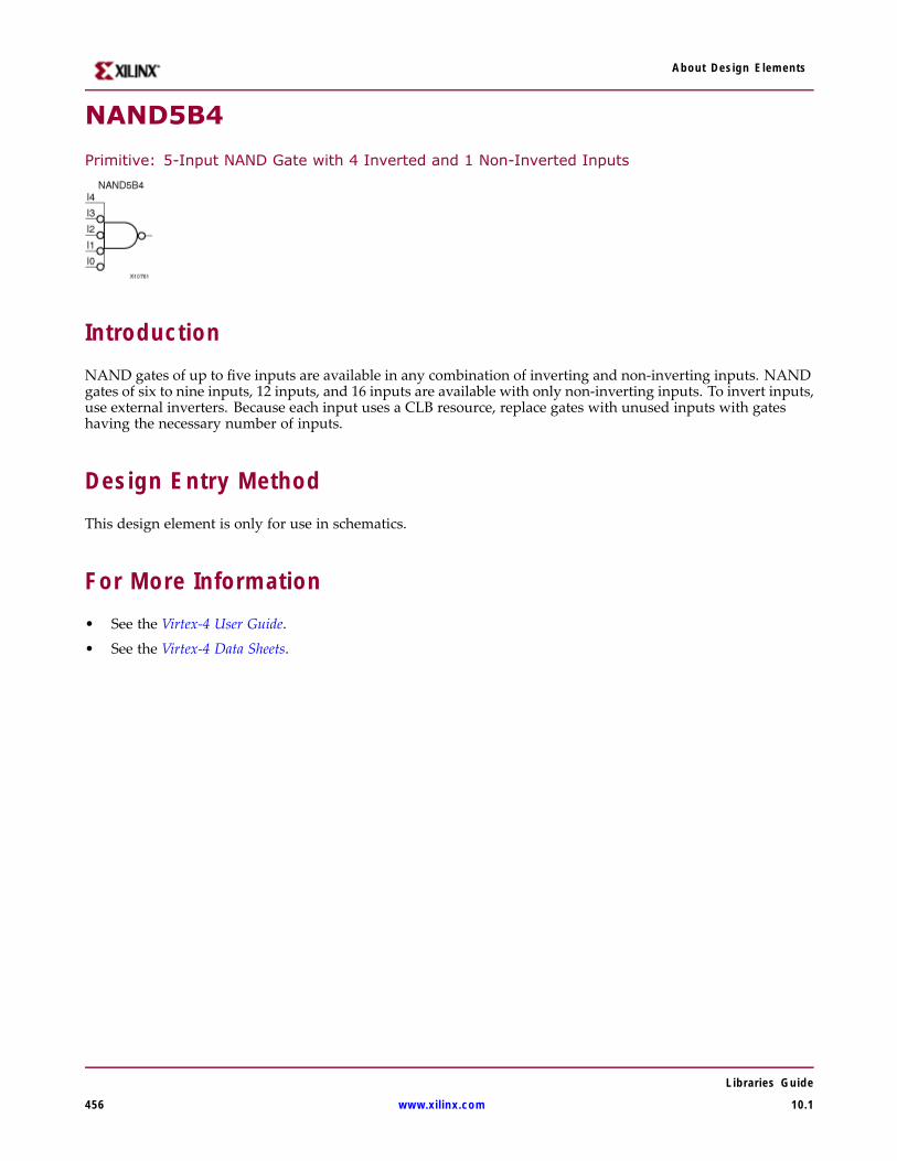
About Design Elements
NAND5B4
Primitive: 5-Input NAND Gate with 4 Inverted and 1 Non-Inverted Inputs
IntroductionNAND gates of up to five inputs are available in any combination of inverting and non-inverting inputs. NANDgates of six to nine inputs, 12 inputs, and 16 inputs are available with only non-inverting inputs. To invert inputs,use external inverters. Because each input uses a CLB resource, replace gates with unused inputs with gateshaving the necessary number of inputs.
Design Entry MethodThis design element is only for use in schematics.
For More Information• See the Virtex-4 User Guide.
• See the Virtex-4 Data Sheets.
Libraries Guide
456 www.xilinx.com 10.1
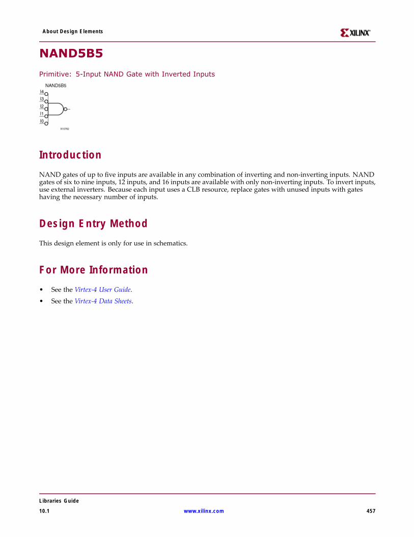
About Design Elements
NAND5B5
Primitive: 5-Input NAND Gate with Inverted Inputs
IntroductionNAND gates of up to five inputs are available in any combination of inverting and non-inverting inputs. NANDgates of six to nine inputs, 12 inputs, and 16 inputs are available with only non-inverting inputs. To invert inputs,use external inverters. Because each input uses a CLB resource, replace gates with unused inputs with gateshaving the necessary number of inputs.
Design Entry MethodThis design element is only for use in schematics.
For More Information• See the Virtex-4 User Guide.
• See the Virtex-4 Data Sheets.
Libraries Guide
10.1 www.xilinx.com 457
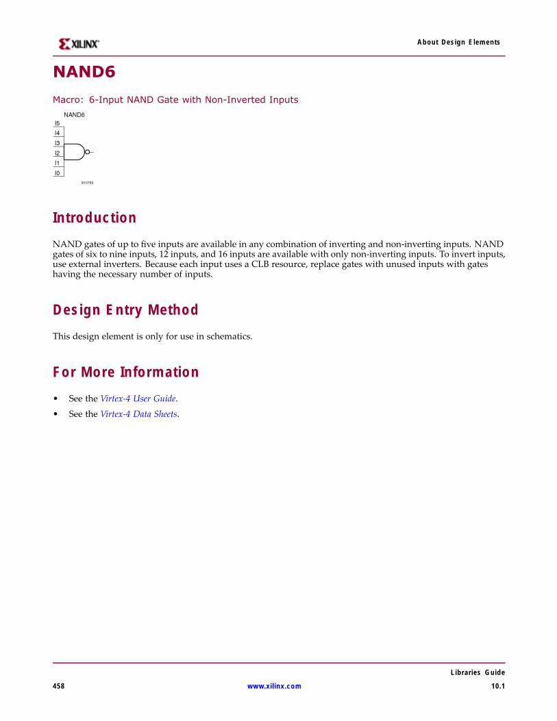
About Design Elements
NAND6
Macro: 6-Input NAND Gate with Non-Inverted Inputs
IntroductionNAND gates of up to five inputs are available in any combination of inverting and non-inverting inputs. NANDgates of six to nine inputs, 12 inputs, and 16 inputs are available with only non-inverting inputs. To invert inputs,use external inverters. Because each input uses a CLB resource, replace gates with unused inputs with gateshaving the necessary number of inputs.
Design Entry MethodThis design element is only for use in schematics.
For More Information• See the Virtex-4 User Guide.
• See the Virtex-4 Data Sheets.
Libraries Guide
458 www.xilinx.com 10.1
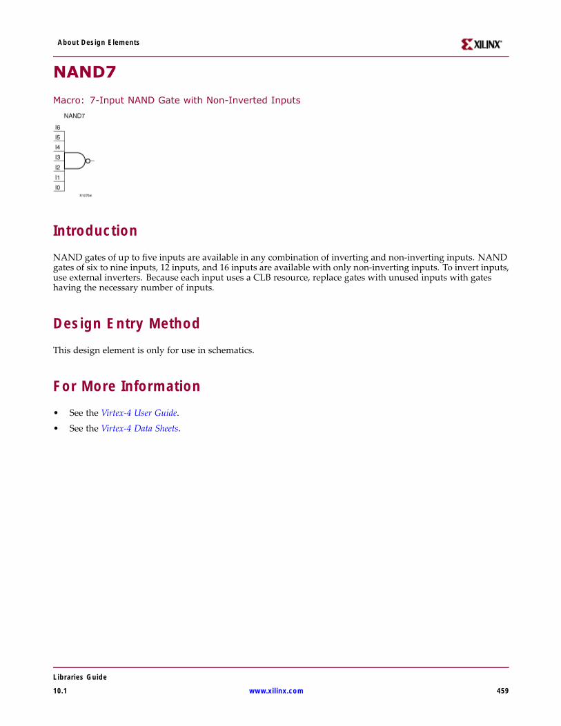
About Design Elements
NAND7
Macro: 7-Input NAND Gate with Non-Inverted Inputs
IntroductionNAND gates of up to five inputs are available in any combination of inverting and non-inverting inputs. NANDgates of six to nine inputs, 12 inputs, and 16 inputs are available with only non-inverting inputs. To invert inputs,use external inverters. Because each input uses a CLB resource, replace gates with unused inputs with gateshaving the necessary number of inputs.
Design Entry MethodThis design element is only for use in schematics.
For More Information• See the Virtex-4 User Guide.
• See the Virtex-4 Data Sheets.
Libraries Guide
10.1 www.xilinx.com 459
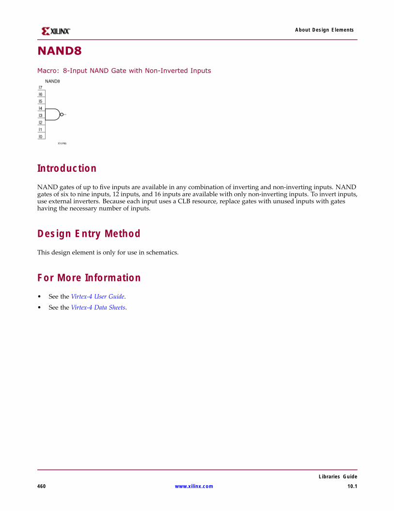
About Design Elements
NAND8
Macro: 8-Input NAND Gate with Non-Inverted Inputs
IntroductionNAND gates of up to five inputs are available in any combination of inverting and non-inverting inputs. NANDgates of six to nine inputs, 12 inputs, and 16 inputs are available with only non-inverting inputs. To invert inputs,use external inverters. Because each input uses a CLB resource, replace gates with unused inputs with gateshaving the necessary number of inputs.
Design Entry MethodThis design element is only for use in schematics.
For More Information• See the Virtex-4 User Guide.
• See the Virtex-4 Data Sheets.
Libraries Guide
460 www.xilinx.com 10.1
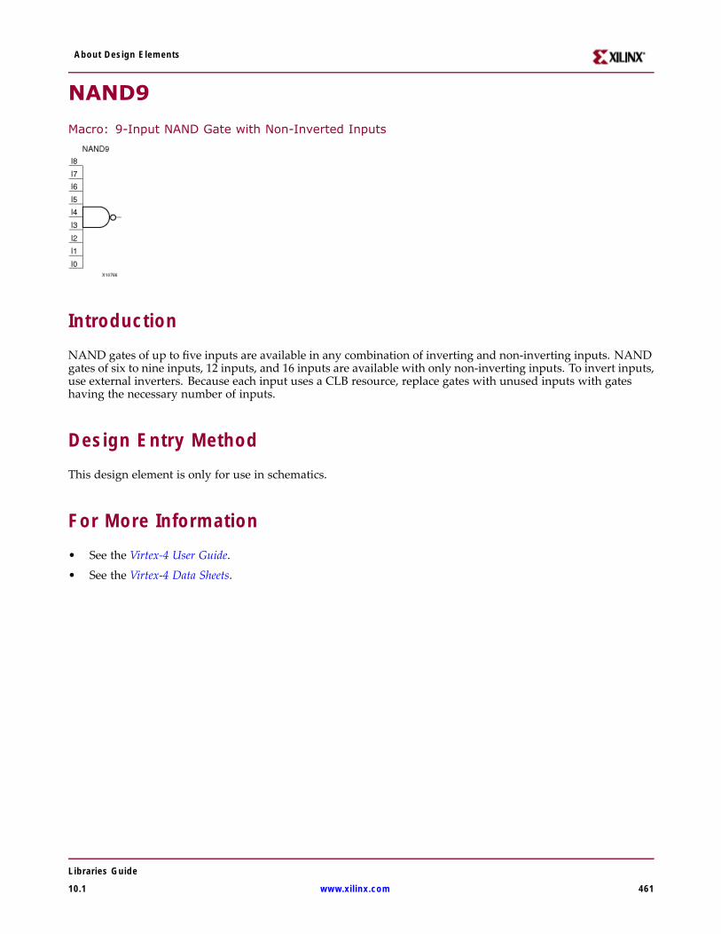
About Design Elements
NAND9
Macro: 9-Input NAND Gate with Non-Inverted Inputs
IntroductionNAND gates of up to five inputs are available in any combination of inverting and non-inverting inputs. NANDgates of six to nine inputs, 12 inputs, and 16 inputs are available with only non-inverting inputs. To invert inputs,use external inverters. Because each input uses a CLB resource, replace gates with unused inputs with gateshaving the necessary number of inputs.
Design Entry MethodThis design element is only for use in schematics.
For More Information• See the Virtex-4 User Guide.
• See the Virtex-4 Data Sheets.
Libraries Guide
10.1 www.xilinx.com 461
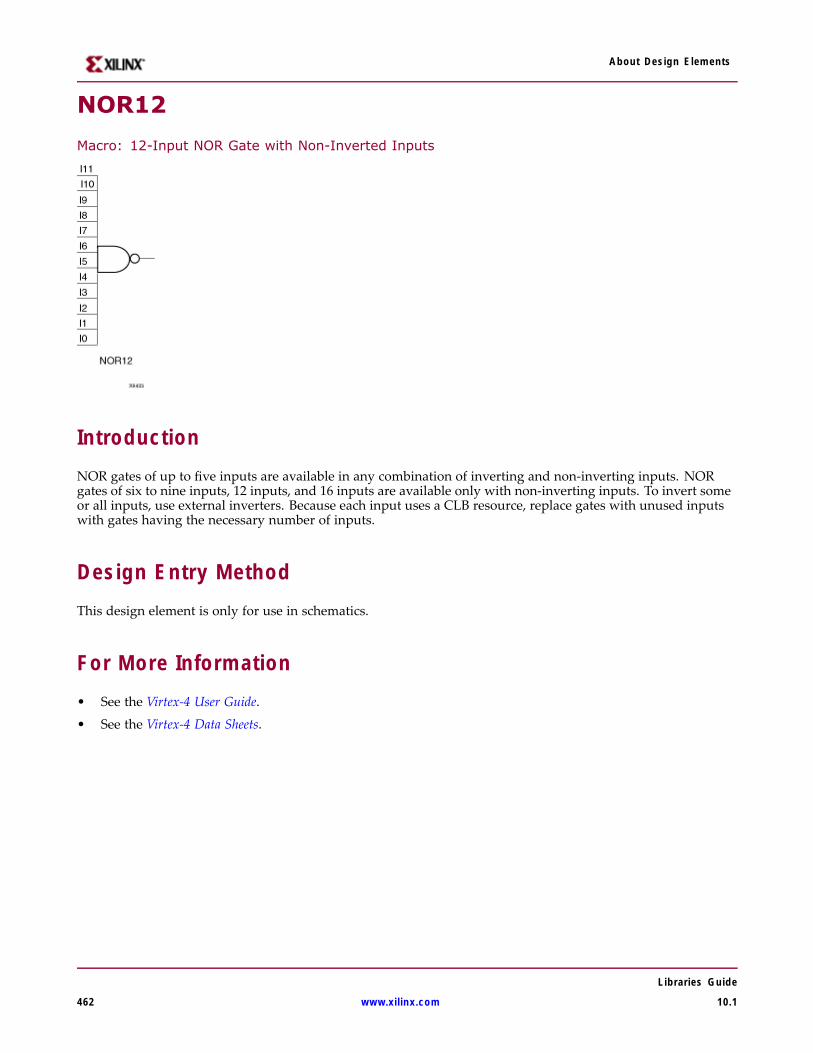
About Design Elements
NOR12
Macro: 12-Input NOR Gate with Non-Inverted Inputs
IntroductionNOR gates of up to five inputs are available in any combination of inverting and non-inverting inputs. NORgates of six to nine inputs, 12 inputs, and 16 inputs are available only with non-inverting inputs. To invert someor all inputs, use external inverters. Because each input uses a CLB resource, replace gates with unused inputswith gates having the necessary number of inputs.
Design Entry MethodThis design element is only for use in schematics.
For More Information• See the Virtex-4 User Guide.
• See the Virtex-4 Data Sheets.
Libraries Guide
462 www.xilinx.com 10.1
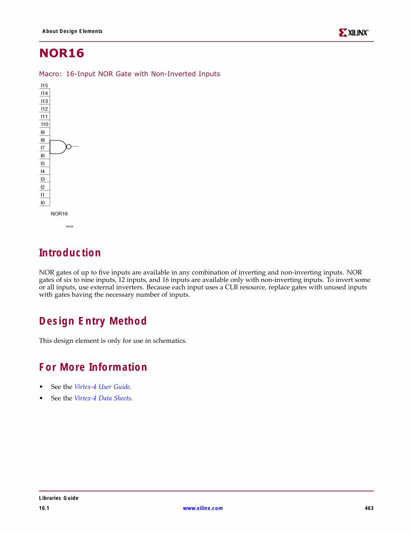
About Design Elements
NOR16
Macro: 16-Input NOR Gate with Non-Inverted Inputs
IntroductionNOR gates of up to five inputs are available in any combination of inverting and non-inverting inputs. NORgates of six to nine inputs, 12 inputs, and 16 inputs are available only with non-inverting inputs. To invert someor all inputs, use external inverters. Because each input uses a CLB resource, replace gates with unused inputswith gates having the necessary number of inputs.
Design Entry MethodThis design element is only for use in schematics.
For More Information• See the Virtex-4 User Guide.
• See the Virtex-4 Data Sheets.
Libraries Guide
10.1 www.xilinx.com 463
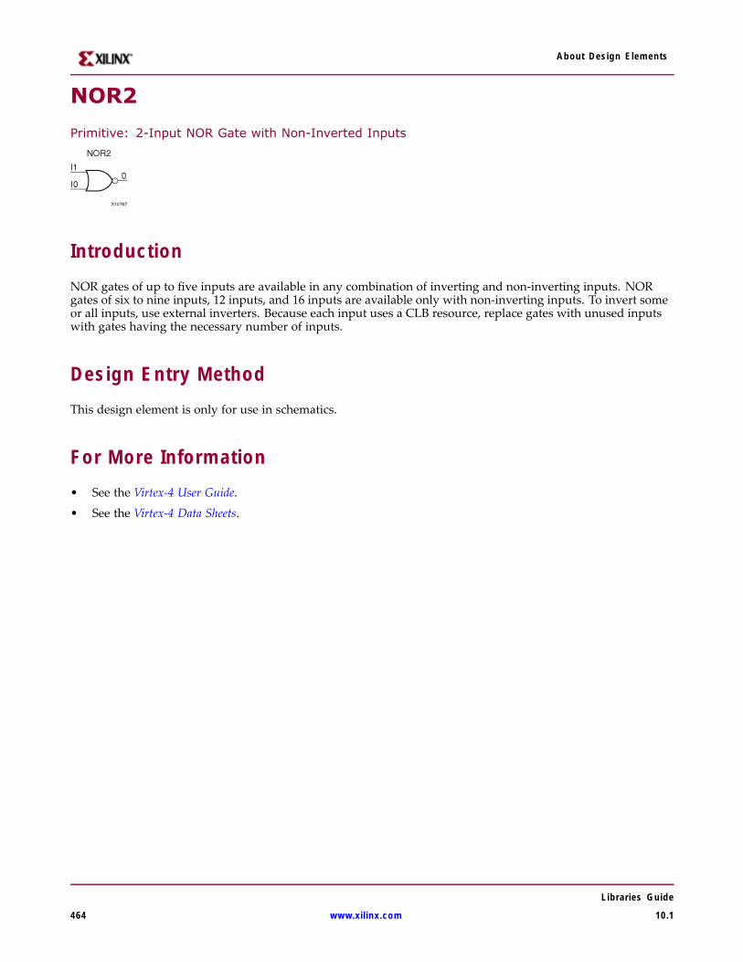
About Design Elements
NOR2
Primitive: 2-Input NOR Gate with Non-Inverted Inputs
IntroductionNOR gates of up to five inputs are available in any combination of inverting and non-inverting inputs. NORgates of six to nine inputs, 12 inputs, and 16 inputs are available only with non-inverting inputs. To invert someor all inputs, use external inverters. Because each input uses a CLB resource, replace gates with unused inputswith gates having the necessary number of inputs.
Design Entry MethodThis design element is only for use in schematics.
For More Information• See the Virtex-4 User Guide.
• See the Virtex-4 Data Sheets.
Libraries Guide
464 www.xilinx.com 10.1
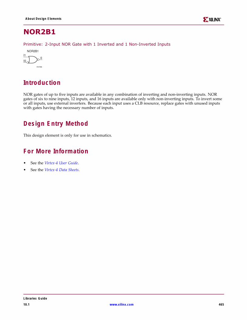
About Design Elements
NOR2B1
Primitive: 2-Input NOR Gate with 1 Inverted and 1 Non-Inverted Inputs
IntroductionNOR gates of up to five inputs are available in any combination of inverting and non-inverting inputs. NORgates of six to nine inputs, 12 inputs, and 16 inputs are available only with non-inverting inputs. To invert someor all inputs, use external inverters. Because each input uses a CLB resource, replace gates with unused inputswith gates having the necessary number of inputs.
Design Entry MethodThis design element is only for use in schematics.
For More Information• See the Virtex-4 User Guide.
• See the Virtex-4 Data Sheets.
Libraries Guide
10.1 www.xilinx.com 465

About Design Elements
NOR2B2
Primitive: 2-Input NOR Gate with Inverted Inputs
IntroductionNOR gates of up to five inputs are available in any combination of inverting and non-inverting inputs. NORgates of six to nine inputs, 12 inputs, and 16 inputs are available only with non-inverting inputs. To invert someor all inputs, use external inverters. Because each input uses a CLB resource, replace gates with unused inputswith gates having the necessary number of inputs.
Design Entry MethodThis design element is only for use in schematics.
For More Information• See the Virtex-4 User Guide.
• See the Virtex-4 Data Sheets.
Libraries Guide
466 www.xilinx.com 10.1

About Design Elements
NOR3
Primitive: 3-Input NOR Gate with Non-Inverted Inputs
IntroductionNOR gates of up to five inputs are available in any combination of inverting and non-inverting inputs. NORgates of six to nine inputs, 12 inputs, and 16 inputs are available only with non-inverting inputs. To invert someor all inputs, use external inverters. Because each input uses a CLB resource, replace gates with unused inputswith gates having the necessary number of inputs.
Design Entry MethodThis design element is only for use in schematics.
For More Information• See the Virtex-4 User Guide.
• See the Virtex-4 Data Sheets.
Libraries Guide
10.1 www.xilinx.com 467
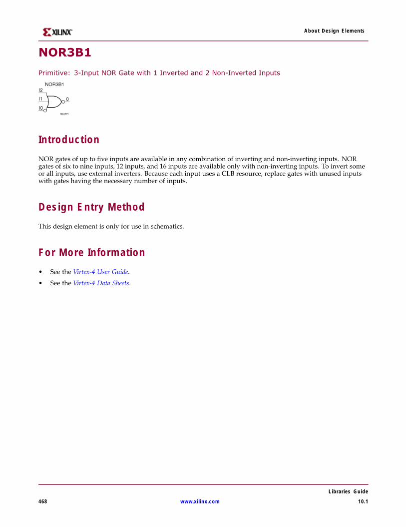
About Design Elements
NOR3B1
Primitive: 3-Input NOR Gate with 1 Inverted and 2 Non-Inverted Inputs
IntroductionNOR gates of up to five inputs are available in any combination of inverting and non-inverting inputs. NORgates of six to nine inputs, 12 inputs, and 16 inputs are available only with non-inverting inputs. To invert someor all inputs, use external inverters. Because each input uses a CLB resource, replace gates with unused inputswith gates having the necessary number of inputs.
Design Entry MethodThis design element is only for use in schematics.
For More Information• See the Virtex-4 User Guide.
• See the Virtex-4 Data Sheets.
Libraries Guide
468 www.xilinx.com 10.1

About Design Elements
NOR3B2
Primitive: 3-Input NOR Gate with 2 Inverted and 1 Non-Inverted Inputs
IntroductionNOR gates of up to five inputs are available in any combination of inverting and non-inverting inputs. NORgates of six to nine inputs, 12 inputs, and 16 inputs are available only with non-inverting inputs. To invert someor all inputs, use external inverters. Because each input uses a CLB resource, replace gates with unused inputswith gates having the necessary number of inputs.
Design Entry MethodThis design element is only for use in schematics.
For More Information• See the Virtex-4 User Guide.
• See the Virtex-4 Data Sheets.
Libraries Guide
10.1 www.xilinx.com 469

About Design Elements
NOR3B3
Primitive: 3-Input NOR Gate with Inverted Inputs
IntroductionNOR gates of up to five inputs are available in any combination of inverting and non-inverting inputs. NORgates of six to nine inputs, 12 inputs, and 16 inputs are available only with non-inverting inputs. To invert someor all inputs, use external inverters. Because each input uses a CLB resource, replace gates with unused inputswith gates having the necessary number of inputs.
Design Entry MethodThis design element is only for use in schematics.
For More Information• See the Virtex-4 User Guide.
• See the Virtex-4 Data Sheets.
Libraries Guide
470 www.xilinx.com 10.1
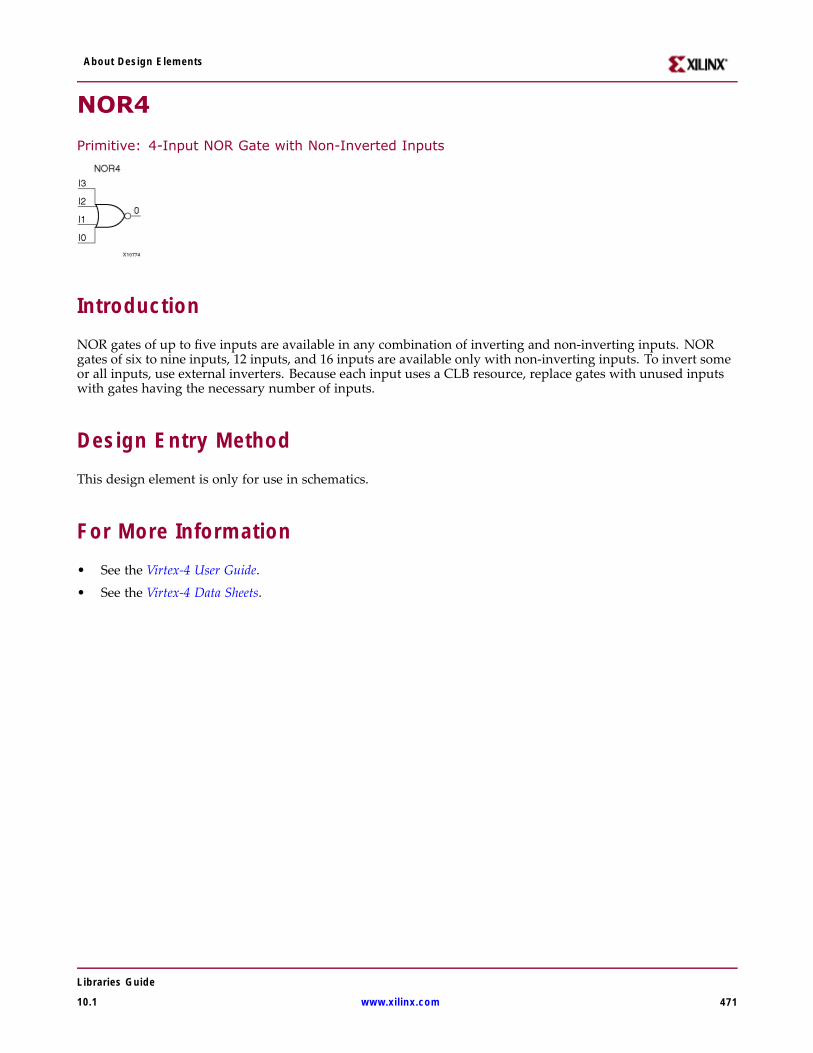
About Design Elements
NOR4
Primitive: 4-Input NOR Gate with Non-Inverted Inputs
IntroductionNOR gates of up to five inputs are available in any combination of inverting and non-inverting inputs. NORgates of six to nine inputs, 12 inputs, and 16 inputs are available only with non-inverting inputs. To invert someor all inputs, use external inverters. Because each input uses a CLB resource, replace gates with unused inputswith gates having the necessary number of inputs.
Design Entry MethodThis design element is only for use in schematics.
For More Information• See the Virtex-4 User Guide.
• See the Virtex-4 Data Sheets.
Libraries Guide
10.1 www.xilinx.com 471

About Design Elements
NOR4B1
Primitive: 4-Input NOR Gate with 1 Inverted and 3 Non-Inverted Inputs
IntroductionNOR gates of up to five inputs are available in any combination of inverting and non-inverting inputs. NORgates of six to nine inputs, 12 inputs, and 16 inputs are available only with non-inverting inputs. To invert someor all inputs, use external inverters. Because each input uses a CLB resource, replace gates with unused inputswith gates having the necessary number of inputs.
Design Entry MethodThis design element is only for use in schematics.
For More Information• See the Virtex-4 User Guide.
• See the Virtex-4 Data Sheets.
Libraries Guide
472 www.xilinx.com 10.1

About Design Elements
NOR4B2
Primitive: 4-Input NOR Gate with 2 Inverted and 2 Non-Inverted Inputs
IntroductionNOR gates of up to five inputs are available in any combination of inverting and non-inverting inputs. NORgates of six to nine inputs, 12 inputs, and 16 inputs are available only with non-inverting inputs. To invert someor all inputs, use external inverters. Because each input uses a CLB resource, replace gates with unused inputswith gates having the necessary number of inputs.
Design Entry MethodThis design element is only for use in schematics.
For More Information• See the Virtex-4 User Guide.
• See the Virtex-4 Data Sheets.
Libraries Guide
10.1 www.xilinx.com 473
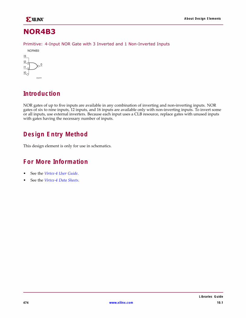
About Design Elements
NOR4B3
Primitive: 4-Input NOR Gate with 3 Inverted and 1 Non-Inverted Inputs
IntroductionNOR gates of up to five inputs are available in any combination of inverting and non-inverting inputs. NORgates of six to nine inputs, 12 inputs, and 16 inputs are available only with non-inverting inputs. To invert someor all inputs, use external inverters. Because each input uses a CLB resource, replace gates with unused inputswith gates having the necessary number of inputs.
Design Entry MethodThis design element is only for use in schematics.
For More Information• See the Virtex-4 User Guide.
• See the Virtex-4 Data Sheets.
Libraries Guide
474 www.xilinx.com 10.1

About Design Elements
NOR4B4
Primitive: 4-Input NOR Gate with Inverted Inputs
IntroductionNOR gates of up to five inputs are available in any combination of inverting and non-inverting inputs. NORgates of six to nine inputs, 12 inputs, and 16 inputs are available only with non-inverting inputs. To invert someor all inputs, use external inverters. Because each input uses a CLB resource, replace gates with unused inputswith gates having the necessary number of inputs.
Design Entry MethodThis design element is only for use in schematics.
For More Information• See the Virtex-4 User Guide.
• See the Virtex-4 Data Sheets.
Libraries Guide
10.1 www.xilinx.com 475
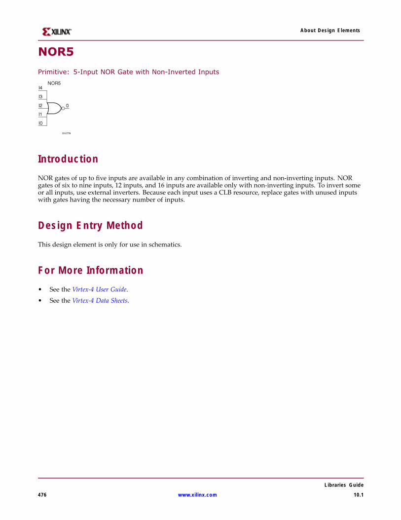
About Design Elements
NOR5
Primitive: 5-Input NOR Gate with Non-Inverted Inputs
IntroductionNOR gates of up to five inputs are available in any combination of inverting and non-inverting inputs. NORgates of six to nine inputs, 12 inputs, and 16 inputs are available only with non-inverting inputs. To invert someor all inputs, use external inverters. Because each input uses a CLB resource, replace gates with unused inputswith gates having the necessary number of inputs.
Design Entry MethodThis design element is only for use in schematics.
For More Information• See the Virtex-4 User Guide.
• See the Virtex-4 Data Sheets.
Libraries Guide
476 www.xilinx.com 10.1
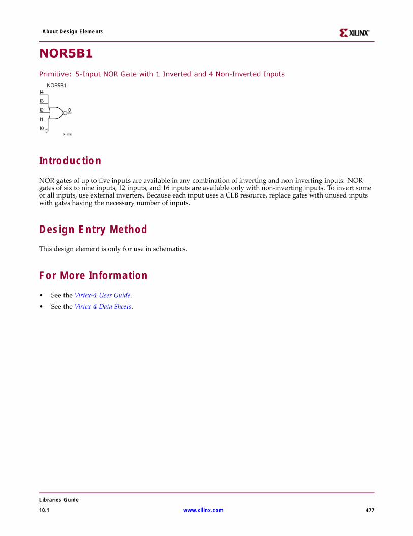
About Design Elements
NOR5B1
Primitive: 5-Input NOR Gate with 1 Inverted and 4 Non-Inverted Inputs
IntroductionNOR gates of up to five inputs are available in any combination of inverting and non-inverting inputs. NORgates of six to nine inputs, 12 inputs, and 16 inputs are available only with non-inverting inputs. To invert someor all inputs, use external inverters. Because each input uses a CLB resource, replace gates with unused inputswith gates having the necessary number of inputs.
Design Entry MethodThis design element is only for use in schematics.
For More Information• See the Virtex-4 User Guide.
• See the Virtex-4 Data Sheets.
Libraries Guide
10.1 www.xilinx.com 477

About Design Elements
NOR5B2
Primitive: 5-Input NOR Gate with 2 Inverted and 3 Non-Inverted Inputs
IntroductionNOR gates of up to five inputs are available in any combination of inverting and non-inverting inputs. NORgates of six to nine inputs, 12 inputs, and 16 inputs are available only with non-inverting inputs. To invert someor all inputs, use external inverters. Because each input uses a CLB resource, replace gates with unused inputswith gates having the necessary number of inputs.
Design Entry MethodThis design element is only for use in schematics.
For More Information• See the Virtex-4 User Guide.
• See the Virtex-4 Data Sheets.
Libraries Guide
478 www.xilinx.com 10.1

About Design Elements
NOR5B3
Primitive: 5-Input NOR Gate with 3 Inverted and 2 Non-Inverted Inputs
IntroductionNOR gates of up to five inputs are available in any combination of inverting and non-inverting inputs. NORgates of six to nine inputs, 12 inputs, and 16 inputs are available only with non-inverting inputs. To invert someor all inputs, use external inverters. Because each input uses a CLB resource, replace gates with unused inputswith gates having the necessary number of inputs.
Design Entry MethodThis design element is only for use in schematics.
For More Information• See the Virtex-4 User Guide.
• See the Virtex-4 Data Sheets.
Libraries Guide
10.1 www.xilinx.com 479
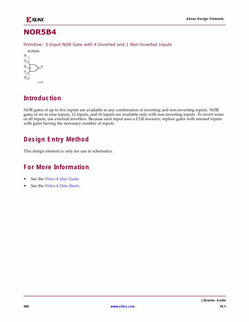
About Design Elements
NOR5B4
Primitive: 5-Input NOR Gate with 4 Inverted and 1 Non-Inverted Inputs
IntroductionNOR gates of up to five inputs are available in any combination of inverting and non-inverting inputs. NORgates of six to nine inputs, 12 inputs, and 16 inputs are available only with non-inverting inputs. To invert someor all inputs, use external inverters. Because each input uses a CLB resource, replace gates with unused inputswith gates having the necessary number of inputs.
Design Entry MethodThis design element is only for use in schematics.
For More Information• See the Virtex-4 User Guide.
• See the Virtex-4 Data Sheets.
Libraries Guide
480 www.xilinx.com 10.1
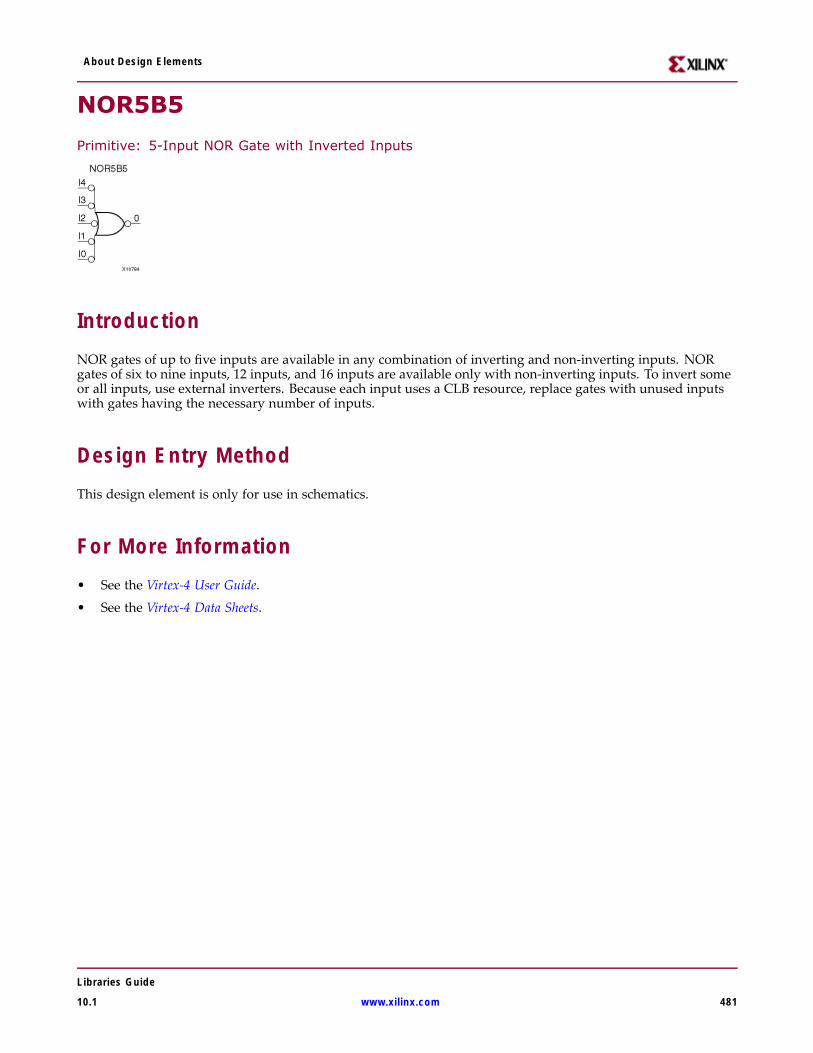
About Design Elements
NOR5B5
Primitive: 5-Input NOR Gate with Inverted Inputs
IntroductionNOR gates of up to five inputs are available in any combination of inverting and non-inverting inputs. NORgates of six to nine inputs, 12 inputs, and 16 inputs are available only with non-inverting inputs. To invert someor all inputs, use external inverters. Because each input uses a CLB resource, replace gates with unused inputswith gates having the necessary number of inputs.
Design Entry MethodThis design element is only for use in schematics.
For More Information• See the Virtex-4 User Guide.
• See the Virtex-4 Data Sheets.
Libraries Guide
10.1 www.xilinx.com 481
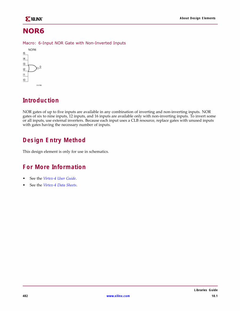
About Design Elements
NOR6
Macro: 6-Input NOR Gate with Non-Inverted Inputs
IntroductionNOR gates of up to five inputs are available in any combination of inverting and non-inverting inputs. NORgates of six to nine inputs, 12 inputs, and 16 inputs are available only with non-inverting inputs. To invert someor all inputs, use external inverters. Because each input uses a CLB resource, replace gates with unused inputswith gates having the necessary number of inputs.
Design Entry MethodThis design element is only for use in schematics.
For More Information• See the Virtex-4 User Guide.
• See the Virtex-4 Data Sheets.
Libraries Guide
482 www.xilinx.com 10.1
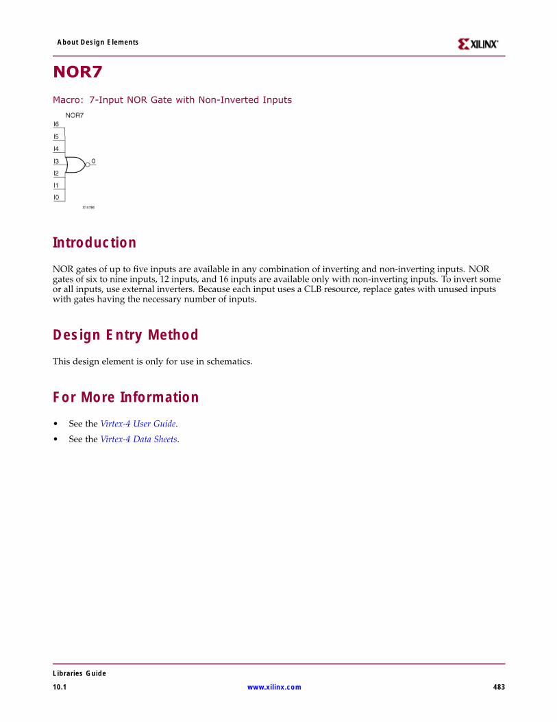
About Design Elements
NOR7
Macro: 7-Input NOR Gate with Non-Inverted Inputs
IntroductionNOR gates of up to five inputs are available in any combination of inverting and non-inverting inputs. NORgates of six to nine inputs, 12 inputs, and 16 inputs are available only with non-inverting inputs. To invert someor all inputs, use external inverters. Because each input uses a CLB resource, replace gates with unused inputswith gates having the necessary number of inputs.
Design Entry MethodThis design element is only for use in schematics.
For More Information• See the Virtex-4 User Guide.
• See the Virtex-4 Data Sheets.
Libraries Guide
10.1 www.xilinx.com 483
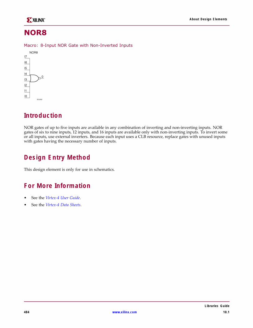
About Design Elements
NOR8
Macro: 8-Input NOR Gate with Non-Inverted Inputs
IntroductionNOR gates of up to five inputs are available in any combination of inverting and non-inverting inputs. NORgates of six to nine inputs, 12 inputs, and 16 inputs are available only with non-inverting inputs. To invert someor all inputs, use external inverters. Because each input uses a CLB resource, replace gates with unused inputswith gates having the necessary number of inputs.
Design Entry MethodThis design element is only for use in schematics.
For More Information• See the Virtex-4 User Guide.
• See the Virtex-4 Data Sheets.
Libraries Guide
484 www.xilinx.com 10.1
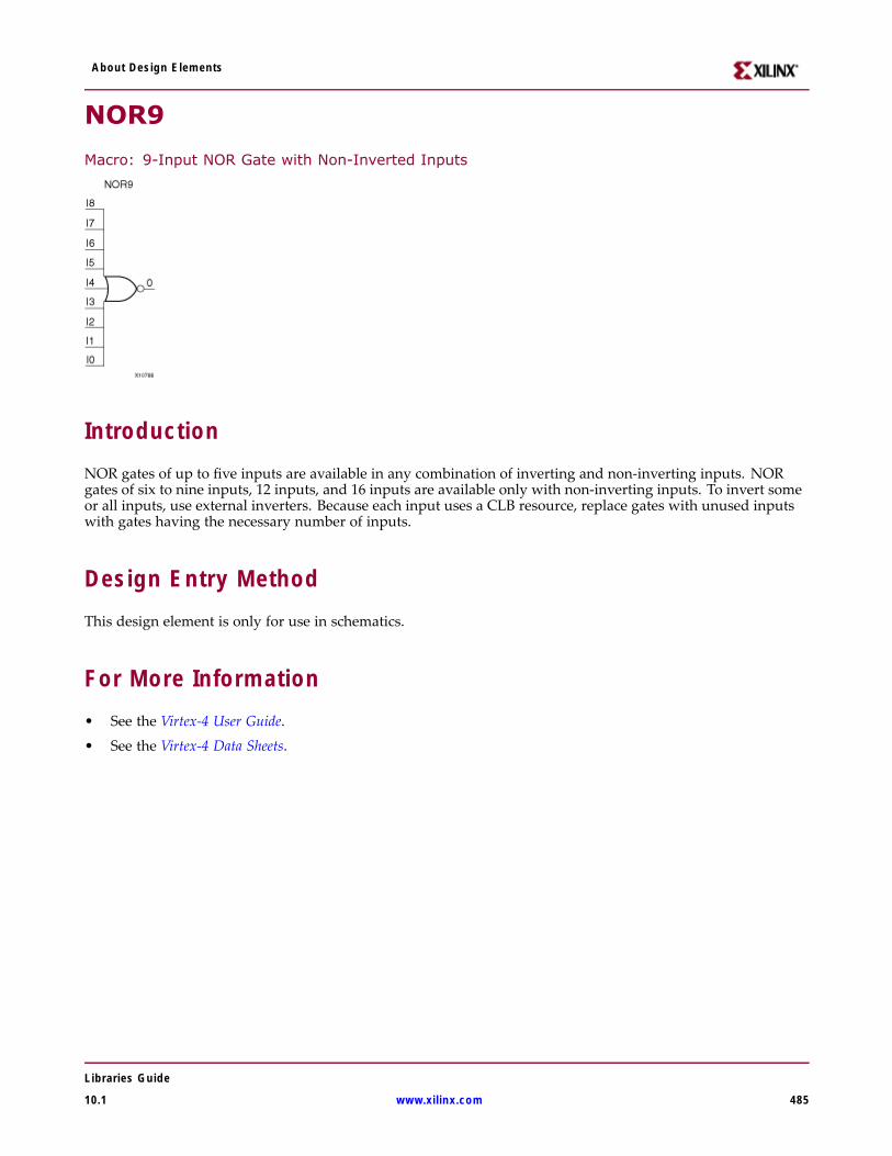
About Design Elements
NOR9
Macro: 9-Input NOR Gate with Non-Inverted Inputs
IntroductionNOR gates of up to five inputs are available in any combination of inverting and non-inverting inputs. NORgates of six to nine inputs, 12 inputs, and 16 inputs are available only with non-inverting inputs. To invert someor all inputs, use external inverters. Because each input uses a CLB resource, replace gates with unused inputswith gates having the necessary number of inputs.
Design Entry MethodThis design element is only for use in schematics.
For More Information• See the Virtex-4 User Guide.
• See the Virtex-4 Data Sheets.
Libraries Guide
10.1 www.xilinx.com 485
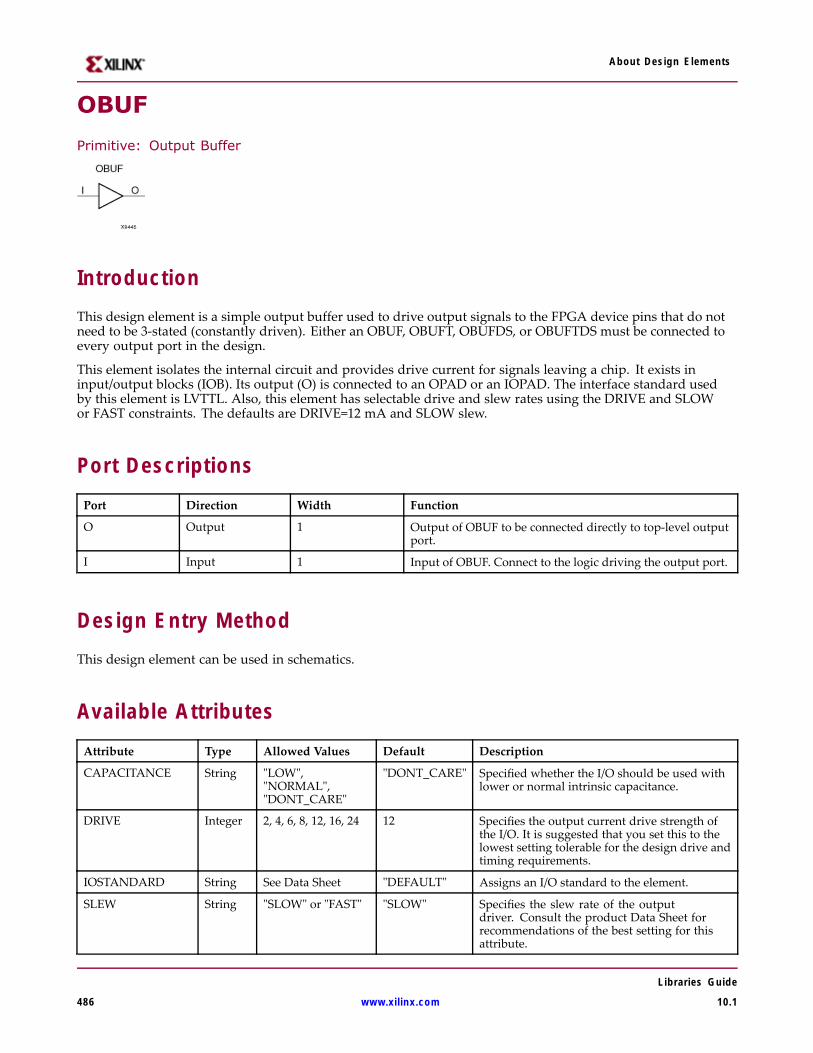
About Design Elements
OBUF
Primitive: Output Buffer
IntroductionThis design element is a simple output buffer used to drive output signals to the FPGA device pins that do notneed to be 3-stated (constantly driven). Either an OBUF, OBUFT, OBUFDS, or OBUFTDS must be connected toevery output port in the design.
This element isolates the internal circuit and provides drive current for signals leaving a chip. It exists ininput/output blocks (IOB). Its output (O) is connected to an OPAD or an IOPAD. The interface standard usedby this element is LVTTL. Also, this element has selectable drive and slew rates using the DRIVE and SLOWor FAST constraints. The defaults are DRIVE=12 mA and SLOW slew.
Port DescriptionsPort Direction Width Function
O Output 1 Output of OBUF to be connected directly to top-level outputport.
I Input 1 Input of OBUF. Connect to the logic driving the output port.
Design Entry MethodThis design element can be used in schematics.
Available AttributesAttribute Type Allowed Values Default Description
CAPACITANCE String "LOW","NORMAL","DONT_CARE"
"DONT_CARE" Specified whether the I/O should be used withlower or normal intrinsic capacitance.
DRIVE Integer 2, 4, 6, 8, 12, 16, 24 12 Specifies the output current drive strength ofthe I/O. It is suggested that you set this to thelowest setting tolerable for the design drive andtiming requirements.
IOSTANDARD String See Data Sheet "DEFAULT" Assigns an I/O standard to the element.
SLEW String "SLOW" or "FAST" "SLOW" Specifies the slew rate of the outputdriver. Consult the product Data Sheet forrecommendations of the best setting for thisattribute.
Libraries Guide
486 www.xilinx.com 10.1

About Design Elements
For More Information• See the Virtex-4 User Guide.
• See the Virtex-4 Data Sheets.
Libraries Guide
10.1 www.xilinx.com 487
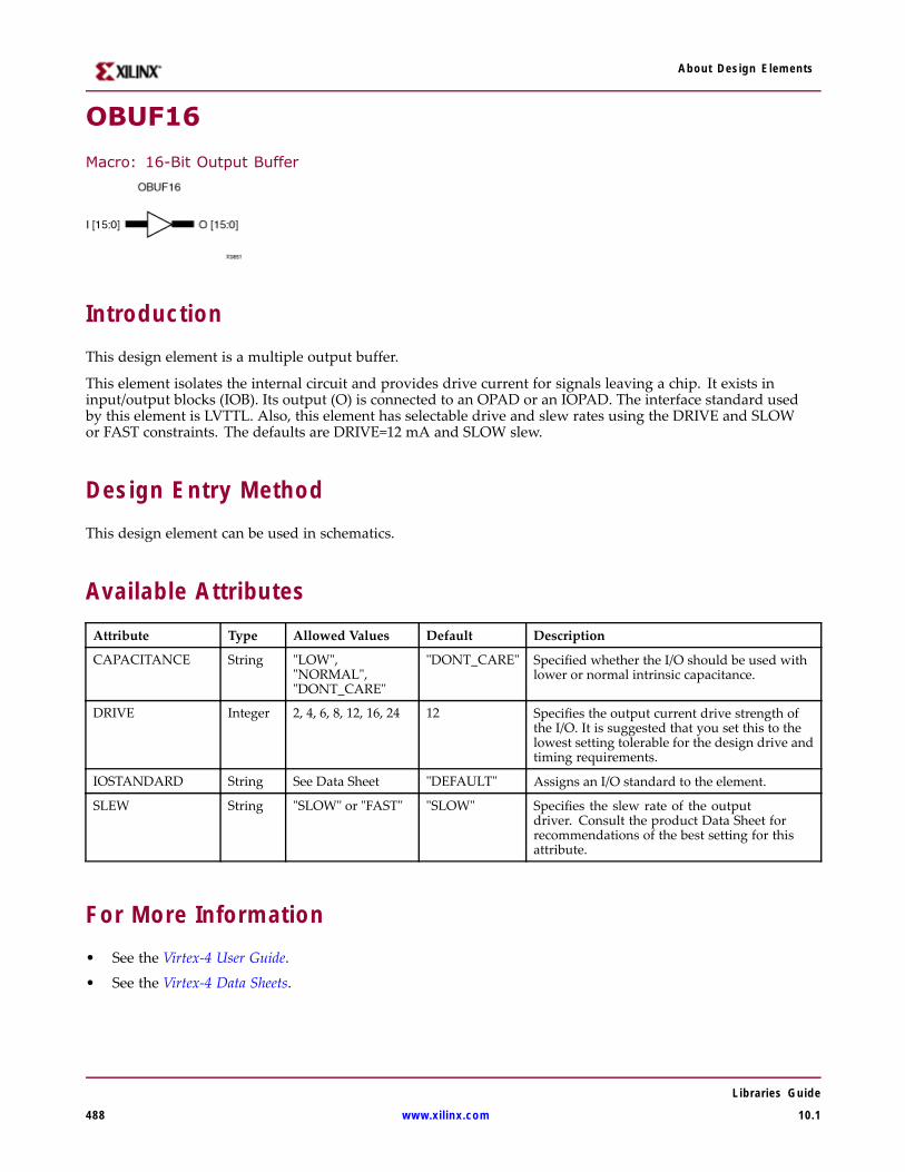
About Design Elements
OBUF16
Macro: 16-Bit Output Buffer
IntroductionThis design element is a multiple output buffer.
This element isolates the internal circuit and provides drive current for signals leaving a chip. It exists ininput/output blocks (IOB). Its output (O) is connected to an OPAD or an IOPAD. The interface standard usedby this element is LVTTL. Also, this element has selectable drive and slew rates using the DRIVE and SLOWor FAST constraints. The defaults are DRIVE=12 mA and SLOW slew.
Design Entry MethodThis design element can be used in schematics.
Available AttributesAttribute Type Allowed Values Default Description
CAPACITANCE String "LOW","NORMAL","DONT_CARE"
"DONT_CARE" Specified whether the I/O should be used withlower or normal intrinsic capacitance.
DRIVE Integer 2, 4, 6, 8, 12, 16, 24 12 Specifies the output current drive strength ofthe I/O. It is suggested that you set this to thelowest setting tolerable for the design drive andtiming requirements.
IOSTANDARD String See Data Sheet "DEFAULT" Assigns an I/O standard to the element.
SLEW String "SLOW" or "FAST" "SLOW" Specifies the slew rate of the outputdriver. Consult the product Data Sheet forrecommendations of the best setting for thisattribute.
For More Information• See the Virtex-4 User Guide.
• See the Virtex-4 Data Sheets.
Libraries Guide
488 www.xilinx.com 10.1
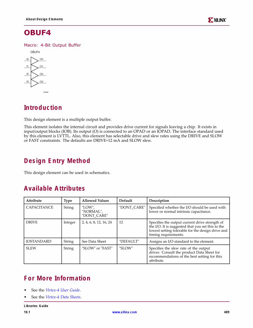
About Design Elements
OBUF4
Macro: 4-Bit Output Buffer
IntroductionThis design element is a multiple output buffer.
This element isolates the internal circuit and provides drive current for signals leaving a chip. It exists ininput/output blocks (IOB). Its output (O) is connected to an OPAD or an IOPAD. The interface standard usedby this element is LVTTL. Also, this element has selectable drive and slew rates using the DRIVE and SLOWor FAST constraints. The defaults are DRIVE=12 mA and SLOW slew.
Design Entry MethodThis design element can be used in schematics.
Available AttributesAttribute Type Allowed Values Default Description
CAPACITANCE String "LOW","NORMAL","DONT_CARE"
"DONT_CARE" Specified whether the I/O should be used withlower or normal intrinsic capacitance.
DRIVE Integer 2, 4, 6, 8, 12, 16, 24 12 Specifies the output current drive strength ofthe I/O. It is suggested that you set this to thelowest setting tolerable for the design drive andtiming requirements.
IOSTANDARD String See Data Sheet "DEFAULT" Assigns an I/O standard to the element.
SLEW String "SLOW" or "FAST" "SLOW" Specifies the slew rate of the outputdriver. Consult the product Data Sheet forrecommendations of the best setting for thisattribute.
For More Information• See the Virtex-4 User Guide.• See the Virtex-4 Data Sheets.
Libraries Guide
10.1 www.xilinx.com 489

About Design Elements
OBUF8
Macro: 8-Bit Output Buffer
IntroductionThis design element is a multiple output buffer.
This element isolates the internal circuit and provides drive current for signals leaving a chip. It exists ininput/output blocks (IOB). Its output (O) is connected to an OPAD or an IOPAD. The interface standard usedby this element is LVTTL. Also, this element has selectable drive and slew rates using the DRIVE and SLOWor FAST constraints. The defaults are DRIVE=12 mA and SLOW slew.
Design Entry MethodThis design element can be used in schematics.
Available AttributesAttribute Type Allowed Values Default Description
CAPACITANCE String "LOW","NORMAL","DONT_CARE"
"DONT_CARE" Specified whether the I/O should be used withlower or normal intrinsic capacitance.
DRIVE Integer 2, 4, 6, 8, 12, 16, 24 12 Specifies the output current drive strength ofthe I/O. It is suggested that you set this to thelowest setting tolerable for the design drive andtiming requirements.
IOSTANDARD String See Data Sheet "DEFAULT" Assigns an I/O standard to the element.
SLEW String "SLOW" or "FAST" "SLOW" Specifies the slew rate of the outputdriver. Consult the product Data Sheet forrecommendations of the best setting for thisattribute.
For More Information• See the Virtex-4 User Guide.
• See the Virtex-4 Data Sheets.
Libraries Guide
490 www.xilinx.com 10.1
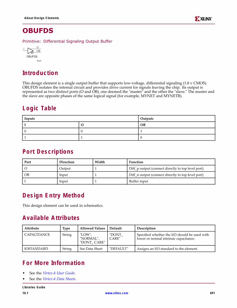
About Design Elements
OBUFDSPrimitive: Differential Signaling Output Buffer
IntroductionThis design element is a single output buffer that supports low-voltage, differential signaling (1.8 v CMOS).OBUFDS isolates the internal circuit and provides drive current for signals leaving the chip. Its output isrepresented as two distinct ports (O and OB), one deemed the "master" and the other the "slave." The master andthe slave are opposite phases of the same logical signal (for example, MYNET and MYNETB).
Logic TableInputs Outputs
I O OB
0 0 1
1 1 0
Port DescriptionsPort Direction Width Function
O Output 1 Diff_p output (connect directly to top level port)
OB Input 1 Diff_n output (connect directly to top level port)
I Input 1 Buffer input
Design Entry MethodThis design element can be used in schematics.
Available AttributesAttribute Type Allowed Values Default Description
CAPACITANCE String "LOW","NORMAL","DONT_ CARE"
"DONT_CARE"
Specified whether the I/O should be used withlower or normal intrinsic capacitance.
IOSTANDARD String See Data Sheet "DEFAULT" Assigns an I/O standard to the element.
For More Information• See the Virtex-4 User Guide.• See the Virtex-4 Data Sheets.
Libraries Guide
10.1 www.xilinx.com 491
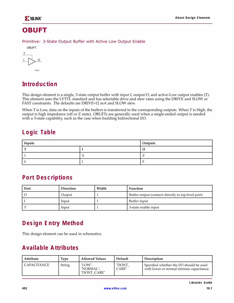
About Design Elements
OBUFT
Primitive: 3-State Output Buffer with Active Low Output Enable
IntroductionThis design element is a single, 3-state output buffer with input I, output O, and active-Low output enables (T).This element uses the LVTTL standard and has selectable drive and slew rates using the DRIVE and SLOW orFAST constraints. The defaults are DRIVE=12 mA and SLOW slew.
When T is Low, data on the inputs of the buffers is transferred to the corresponding outputs. When T is High, theoutput is high impedance (off or Z state). OBUFTs are generally used when a single-ended output is neededwith a 3-state capability, such as the case when building bidirectional I/O.
Logic TableInputs Outputs
T I O
1 X Z
0 I F
Port DescriptionsPort Direction Width Function
O Output 1 Buffer output (connect directly to top-level port)
I Input 1 Buffer input
T Input 1 3-state enable input
Design Entry MethodThis design element can be used in schematics.
Available AttributesAttribute Type Allowed Values Default Description
CAPACITANCE String "LOW","NORMAL","DONT_CARE"
"DONT_CARE"
Specified whether the I/O should be usedwith lower or normal intrinsic capacitance.
Libraries Guide
492 www.xilinx.com 10.1
About Design Elements
Attribute Type Allowed Values Default Description
DRIVE Integer 2, 4, 6, 8, 12, 16, 24 12 Specifies the output current drive strengthof the I/O. It is suggested that you set thisto the lowest setting tolerable for the designdrive and timing requirements.
IOSTANDARD String See Data Sheet "DEFAULT" Assigns an I/O standard to the element.
SLEW String "SLOW" or "FAST” "SLOW" Specifies the slew rate of the output driver.See the Data Sheet for recommendations ofthe best setting for this attribute.
For More Information• See the Virtex-4 User Guide.
• See the Virtex-4 Data Sheets.
Libraries Guide
10.1 www.xilinx.com 493
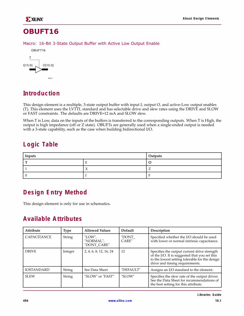
About Design Elements
OBUFT16
Macro: 16-Bit 3-State Output Buffer with Active Low Output Enable
IntroductionThis design element is a multiple, 3-state output buffer with input I, output O, and active-Low output enables(T). This element uses the LVTTL standard and has selectable drive and slew rates using the DRIVE and SLOWor FAST constraints. The defaults are DRIVE=12 mA and SLOW slew.
When T is Low, data on the inputs of the buffers is transferred to the corresponding outputs. When T is High, theoutput is high impedance (off or Z state). OBUFTs are generally used when a single-ended output is neededwith a 3-state capability, such as the case when building bidirectional I/O.
Logic TableInputs Outputs
T I O
1 X Z
0 I F
Design Entry MethodThis design element is only for use in schematics.
Available AttributesAttribute Type Allowed Values Default Description
CAPACITANCE String "LOW","NORMAL","DONT_CARE"
"DONT_CARE"
Specified whether the I/O should be usedwith lower or normal intrinsic capacitance.
DRIVE Integer 2, 4, 6, 8, 12, 16, 24 12 Specifies the output current drive strengthof the I/O. It is suggested that you set thisto the lowest setting tolerable for the designdrive and timing requirements.
IOSTANDARD String See Data Sheet "DEFAULT" Assigns an I/O standard to the element.
SLEW String "SLOW" or "FAST” "SLOW" Specifies the slew rate of the output driver.See the Data Sheet for recommendations ofthe best setting for this attribute.
Libraries Guide
494 www.xilinx.com 10.1

About Design Elements
For More Information• See the Virtex-4 User Guide.
• See the Virtex-4 Data Sheets.
Libraries Guide
10.1 www.xilinx.com 495
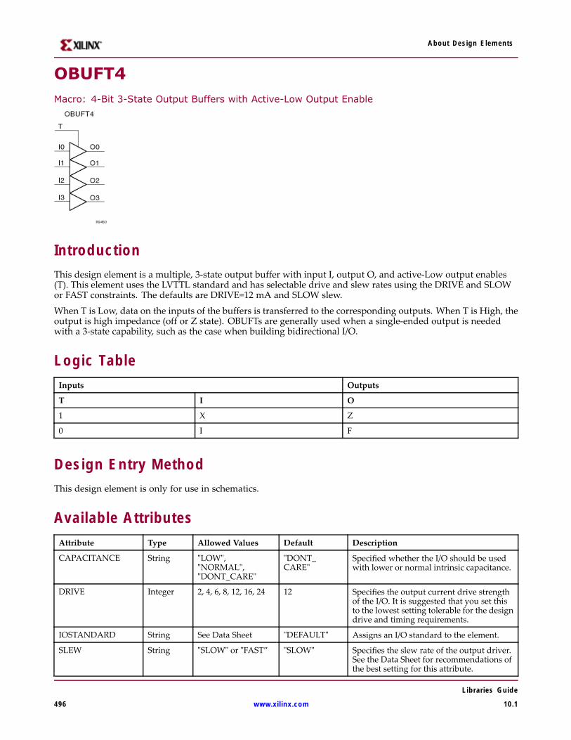
About Design Elements
OBUFT4Macro: 4-Bit 3-State Output Buffers with Active-Low Output Enable
IntroductionThis design element is a multiple, 3-state output buffer with input I, output O, and active-Low output enables(T). This element uses the LVTTL standard and has selectable drive and slew rates using the DRIVE and SLOWor FAST constraints. The defaults are DRIVE=12 mA and SLOW slew.
When T is Low, data on the inputs of the buffers is transferred to the corresponding outputs. When T is High, theoutput is high impedance (off or Z state). OBUFTs are generally used when a single-ended output is neededwith a 3-state capability, such as the case when building bidirectional I/O.
Logic TableInputs Outputs
T I O
1 X Z
0 I F
Design Entry MethodThis design element is only for use in schematics.
Available AttributesAttribute Type Allowed Values Default Description
CAPACITANCE String "LOW","NORMAL","DONT_CARE"
"DONT_CARE"
Specified whether the I/O should be usedwith lower or normal intrinsic capacitance.
DRIVE Integer 2, 4, 6, 8, 12, 16, 24 12 Specifies the output current drive strengthof the I/O. It is suggested that you set thisto the lowest setting tolerable for the designdrive and timing requirements.
IOSTANDARD String See Data Sheet "DEFAULT" Assigns an I/O standard to the element.
SLEW String "SLOW" or "FAST” "SLOW" Specifies the slew rate of the output driver.See the Data Sheet for recommendations ofthe best setting for this attribute.
Libraries Guide
496 www.xilinx.com 10.1

About Design Elements
For More Information• See the Virtex-4 User Guide.
• See the Virtex-4 Data Sheets.
Libraries Guide
10.1 www.xilinx.com 497
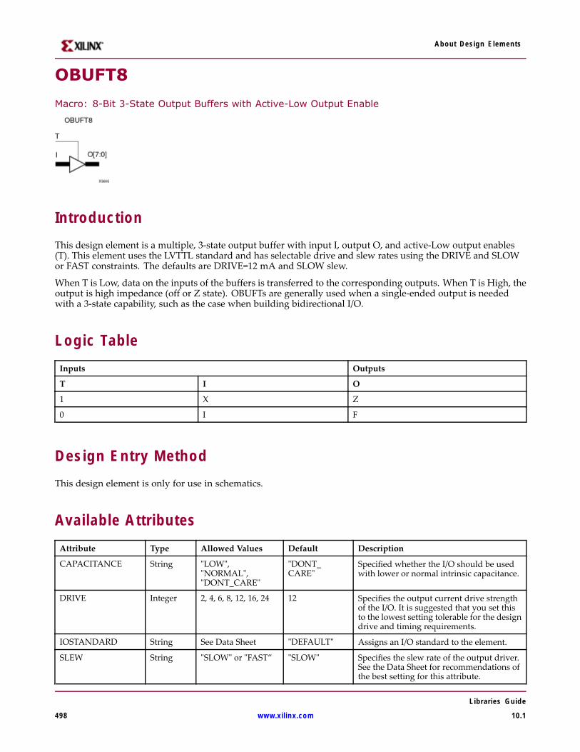
About Design Elements
OBUFT8
Macro: 8-Bit 3-State Output Buffers with Active-Low Output Enable
IntroductionThis design element is a multiple, 3-state output buffer with input I, output O, and active-Low output enables(T). This element uses the LVTTL standard and has selectable drive and slew rates using the DRIVE and SLOWor FAST constraints. The defaults are DRIVE=12 mA and SLOW slew.
When T is Low, data on the inputs of the buffers is transferred to the corresponding outputs. When T is High, theoutput is high impedance (off or Z state). OBUFTs are generally used when a single-ended output is neededwith a 3-state capability, such as the case when building bidirectional I/O.
Logic TableInputs Outputs
T I O
1 X Z
0 I F
Design Entry MethodThis design element is only for use in schematics.
Available AttributesAttribute Type Allowed Values Default Description
CAPACITANCE String "LOW","NORMAL","DONT_CARE"
"DONT_CARE"
Specified whether the I/O should be usedwith lower or normal intrinsic capacitance.
DRIVE Integer 2, 4, 6, 8, 12, 16, 24 12 Specifies the output current drive strengthof the I/O. It is suggested that you set thisto the lowest setting tolerable for the designdrive and timing requirements.
IOSTANDARD String See Data Sheet "DEFAULT" Assigns an I/O standard to the element.
SLEW String "SLOW" or "FAST” "SLOW" Specifies the slew rate of the output driver.See the Data Sheet for recommendations ofthe best setting for this attribute.
Libraries Guide
498 www.xilinx.com 10.1

About Design Elements
For More Information• See the Virtex-4 User Guide.
• See the Virtex-4 Data Sheets.
Libraries Guide
10.1 www.xilinx.com 499
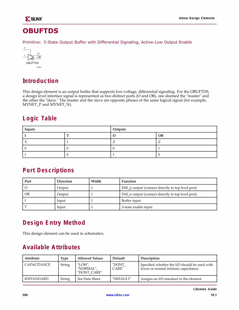
About Design Elements
OBUFTDS
Primitive: 3-State Output Buffer with Differential Signaling, Active-Low Output Enable
IntroductionThis design element is an output buffer that supports low-voltage, differential signaling. For the OBUFTDS,a design level interface signal is represented as two distinct ports (O and OB), one deemed the "master" andthe other the "slave." The master and the slave are opposite phases of the same logical signal (for example,MYNET_P and MYNET_N).
Logic TableInputs Outputs
I T O OB
X 1 Z Z
0 0 0 1
1 0 1 0
Port DescriptionsPort Direction Width Function
O Output 1 Diff_p output (connect directly to top level port)
OB Output 1 Diff_n output (connect directly to top level port)
I Input 1 Buffer input
T Input 1 3-state enable input
Design Entry MethodThis design element can be used in schematics.
Available AttributesAttribute Type Allowed Values Default Description
CAPACITANCE String "LOW","NORMAL","DONT_CARE"
"DONT_CARE"
Specified whether the I/O should be used withlower or normal intrinsic capacitance.
IOSTANDARD String See Data Sheet "DEFAULT" Assigns an I/O standard to the element.
Libraries Guide
500 www.xilinx.com 10.1

About Design Elements
For More Information• See the Virtex-4 User Guide.
• See the Virtex-4 Data Sheets.
Libraries Guide
10.1 www.xilinx.com 501
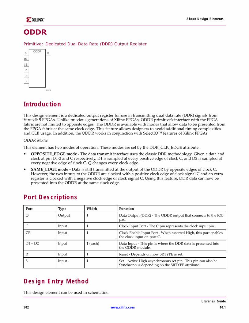
About Design Elements
ODDR
Primitive: Dedicated Dual Data Rate (DDR) Output Register
IntroductionThis design element is a dedicated output register for use in transmitting dual data rate (DDR) signals fromVirtex®-5 FPGAs. Unlike previous generations of Xilinx FPGAs, ODDR primitive’s interface with the FPGAfabric are not limited to opposite edges. The ODDR is available with modes that allow data to be presented fromthe FPGA fabric at the same clock edge. This feature allows designers to avoid additional timing complexitiesand CLB usage. In addition, the ODDR works in conjunction with SelectIO™ features of Xilinx FPGAs.
ODDR Modes
This element has two modes of operation. These modes are set by the DDR_CLK_EDGE attribute.• OPPOSITE_EDGE mode - The data transmit interface uses the classic DDR methodology. Given a data and
clock at pin D1-2 and C respectively, D1 is sampled at every positive edge of clock C, and D2 is sampled atevery negative edge of clock C. Q changes every clock edge.
• SAME_EDGE mode - Data is still transmitted at the output of the ODDR by opposite edges of clock C.However, the two inputs to the ODDR are clocked with a positive clock edge of clock signal C and an extraregister is clocked with a negative clock edge of clock signal C. Using this feature, DDR data can now bepresented into the ODDR at the same clock edge.
Port DescriptionsPort Type Width Function
Q Output 1 Data Output (DDR) - The ODDR output that connects to the IOBpad.
C Input 1 Clock Input Port - The C pin represents the clock input pin.
CE Input 1 Clock Enable Input Port - When asserted High, this port enablesthe clock input on port C.
D1 – D2 Input 1 (each) Data Input - This pin is where the DDR data is presented intothe ODDR module.
R Input 1 Reset - Depends on how SRTYPE is set.
S Input 1 Set - Active High asynchronous set pin. This pin can also beSynchronous depending on the SRTYPE attribute.
Design Entry MethodThis design element can be used in schematics.
Libraries Guide
502 www.xilinx.com 10.1

About Design Elements
Available AttributesAttribute Type Allowed Values Default Description
DDR_CLK_EDGE
String "OPPOSITE_EDGE","SAME_EDGE"
"OPPOSITE_EDGE"
DDR clock mode recovery modeselection.
INIT Integer 0 or 1 1 Q initialization value.
SRTYPE String "SYNC" or "ASYNC" "SYNC" Set/Reset type selection.
For More Information• See the Virtex-4 User Guide.
• See the Virtex-4 Data Sheets.
Libraries Guide
10.1 www.xilinx.com 503
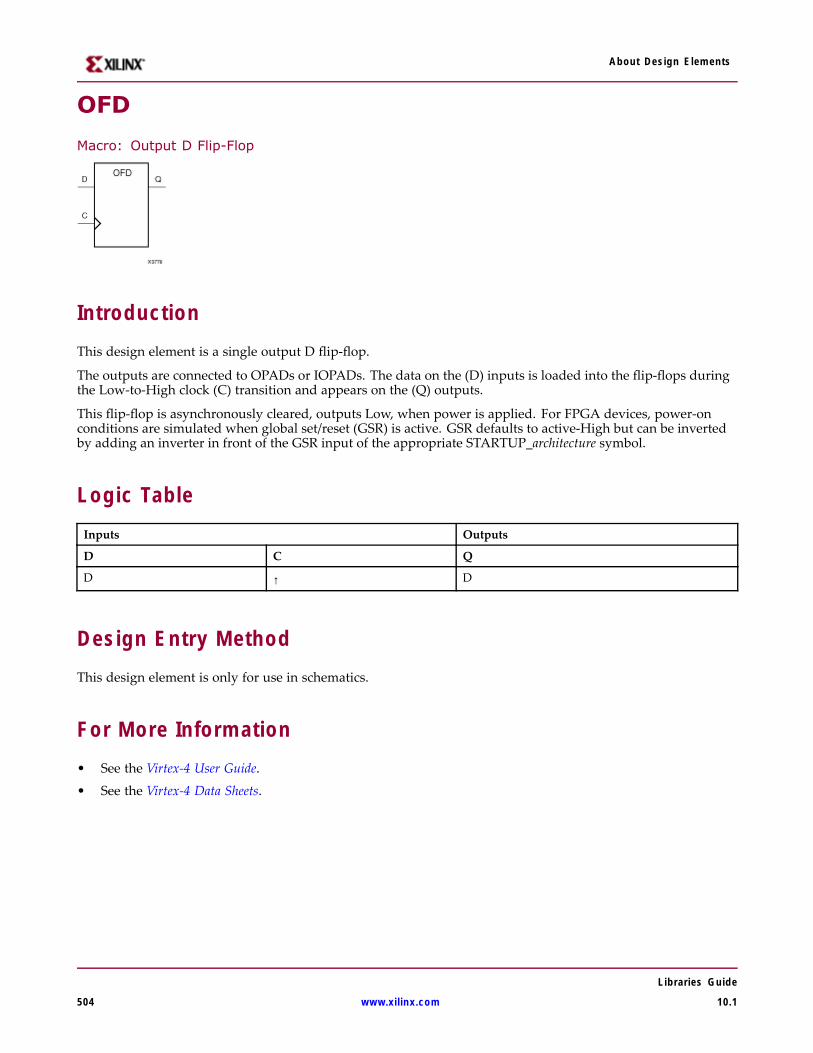
About Design Elements
OFD
Macro: Output D Flip-Flop
IntroductionThis design element is a single output D flip-flop.
The outputs are connected to OPADs or IOPADs. The data on the (D) inputs is loaded into the flip-flops duringthe Low-to-High clock (C) transition and appears on the (Q) outputs.
This flip-flop is asynchronously cleared, outputs Low, when power is applied. For FPGA devices, power-onconditions are simulated when global set/reset (GSR) is active. GSR defaults to active-High but can be invertedby adding an inverter in front of the GSR input of the appropriate STARTUP_architecture symbol.
Logic TableInputs Outputs
D C Q
D ↑ D
Design Entry MethodThis design element is only for use in schematics.
For More Information• See the Virtex-4 User Guide.
• See the Virtex-4 Data Sheets.
Libraries Guide
504 www.xilinx.com 10.1
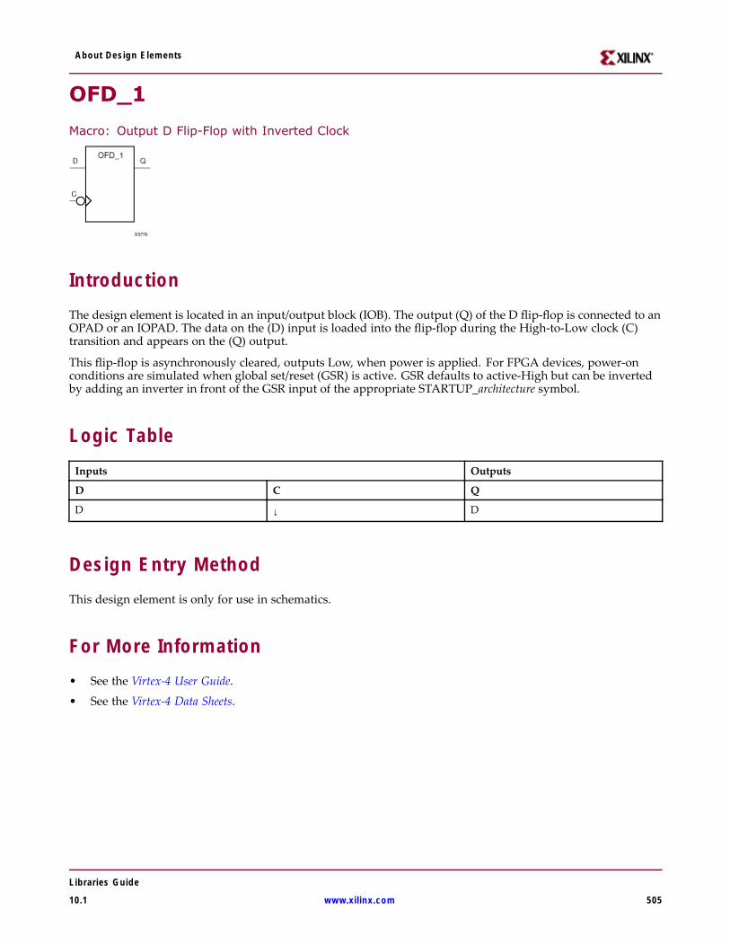
About Design Elements
OFD_1
Macro: Output D Flip-Flop with Inverted Clock
IntroductionThe design element is located in an input/output block (IOB). The output (Q) of the D flip-flop is connected to anOPAD or an IOPAD. The data on the (D) input is loaded into the flip-flop during the High-to-Low clock (C)transition and appears on the (Q) output.
This flip-flop is asynchronously cleared, outputs Low, when power is applied. For FPGA devices, power-onconditions are simulated when global set/reset (GSR) is active. GSR defaults to active-High but can be invertedby adding an inverter in front of the GSR input of the appropriate STARTUP_architecture symbol.
Logic TableInputs Outputs
D C Q
D ↓ D
Design Entry MethodThis design element is only for use in schematics.
For More Information• See the Virtex-4 User Guide.
• See the Virtex-4 Data Sheets.
Libraries Guide
10.1 www.xilinx.com 505
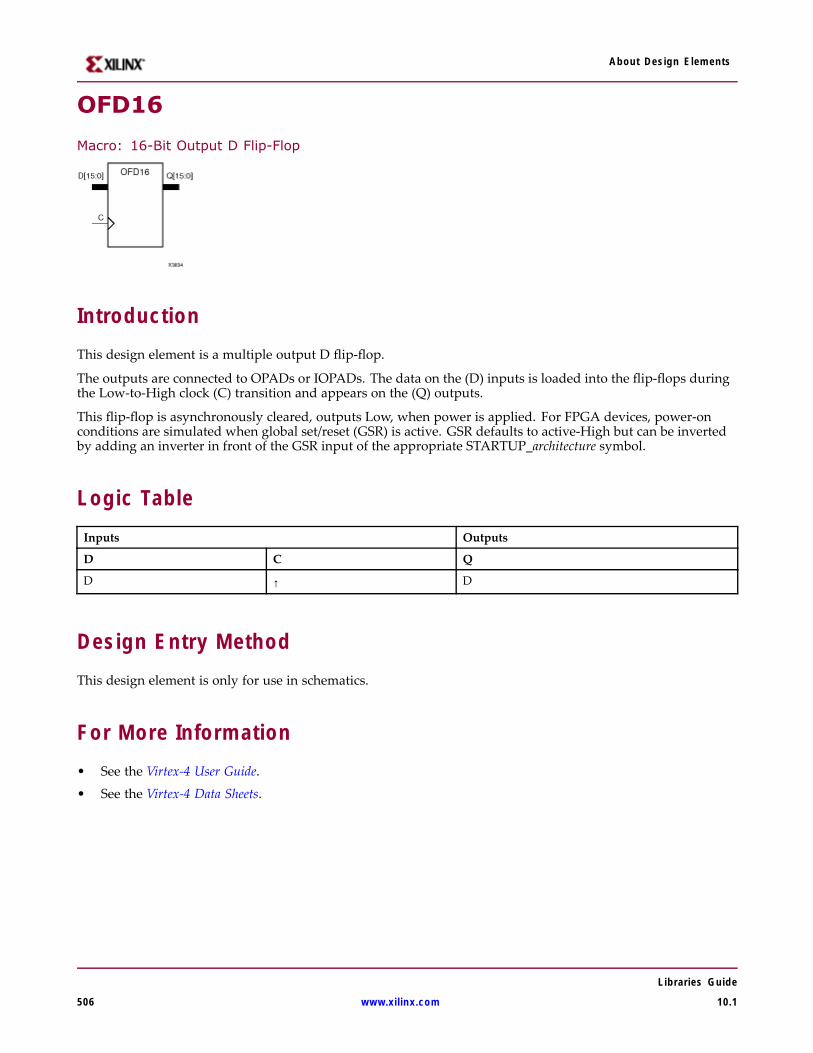
About Design Elements
OFD16
Macro: 16-Bit Output D Flip-Flop
IntroductionThis design element is a multiple output D flip-flop.
The outputs are connected to OPADs or IOPADs. The data on the (D) inputs is loaded into the flip-flops duringthe Low-to-High clock (C) transition and appears on the (Q) outputs.
This flip-flop is asynchronously cleared, outputs Low, when power is applied. For FPGA devices, power-onconditions are simulated when global set/reset (GSR) is active. GSR defaults to active-High but can be invertedby adding an inverter in front of the GSR input of the appropriate STARTUP_architecture symbol.
Logic TableInputs Outputs
D C Q
D ↑ D
Design Entry MethodThis design element is only for use in schematics.
For More Information• See the Virtex-4 User Guide.
• See the Virtex-4 Data Sheets.
Libraries Guide
506 www.xilinx.com 10.1
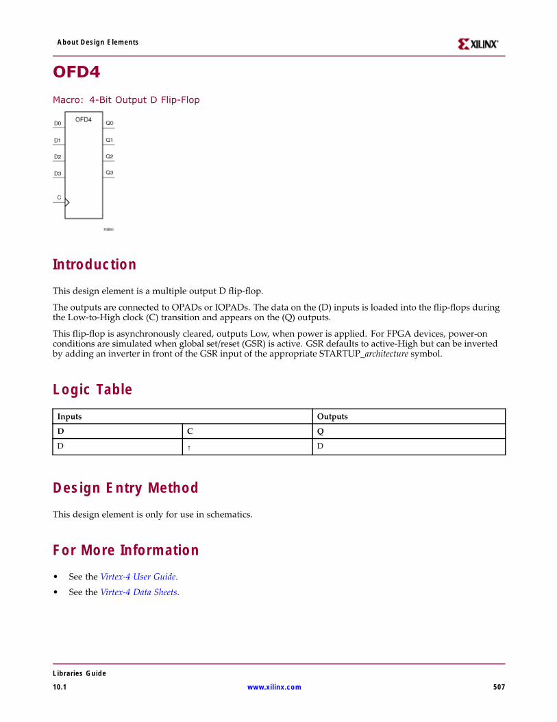
About Design Elements
OFD4
Macro: 4-Bit Output D Flip-Flop
IntroductionThis design element is a multiple output D flip-flop.
The outputs are connected to OPADs or IOPADs. The data on the (D) inputs is loaded into the flip-flops duringthe Low-to-High clock (C) transition and appears on the (Q) outputs.
This flip-flop is asynchronously cleared, outputs Low, when power is applied. For FPGA devices, power-onconditions are simulated when global set/reset (GSR) is active. GSR defaults to active-High but can be invertedby adding an inverter in front of the GSR input of the appropriate STARTUP_architecture symbol.
Logic TableInputs Outputs
D C Q
D ↑ D
Design Entry MethodThis design element is only for use in schematics.
For More Information• See the Virtex-4 User Guide.
• See the Virtex-4 Data Sheets.
Libraries Guide
10.1 www.xilinx.com 507

About Design Elements
OFD8
Macro: 8-Bit Output D Flip-Flop
IntroductionThis design element is a multiple output D flip-flop.
The outputs are connected to OPADs or IOPADs. The data on the (D) inputs is loaded into the flip-flops duringthe Low-to-High clock (C) transition and appears on the (Q) outputs.
This flip-flop is asynchronously cleared, outputs Low, when power is applied. For FPGA devices, power-onconditions are simulated when global set/reset (GSR) is active. GSR defaults to active-High but can be invertedby adding an inverter in front of the GSR input of the appropriate STARTUP_architecture symbol.
Logic TableInputs Outputs
D C Q
D ↑ D
Design Entry MethodThis design element is only for use in schematics.
For More Information• See the Virtex-4 User Guide.
• See the Virtex-4 Data Sheets.
Libraries Guide
508 www.xilinx.com 10.1
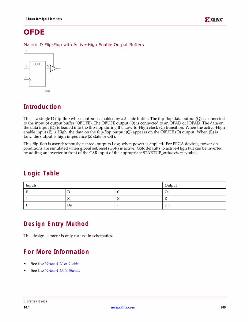
About Design Elements
OFDE
Macro: D Flip-Flop with Active-High Enable Output Buffers
IntroductionThis is a single D flip-flop whose output is enabled by a 3-state buffer. The flip-flop data output (Q) is connectedto the input of output buffer (OBUFE). The OBUFE output (O) is connected to an OPAD or IOPAD. The data onthe data input (D) is loaded into the flip-flop during the Low-to-High clock (C) transition. When the active-Highenable input (E) is High, the data on the flip-flop output (Q) appears on the OBUFE (O) output. When (E) isLow, the output is high impedance (Z state or Off).
This flip-flop is asynchronously cleared, outputs Low, when power is applied. For FPGA devices, power-onconditions are simulated when global set/reset (GSR) is active. GSR defaults to active-High but can be invertedby adding an inverter in front of the GSR input of the appropriate STARTUP_architecture symbol.
Logic TableInputs Output
E D C O
0 X X Z
1 Dn ↑ Dn
Design Entry MethodThis design element is only for use in schematics.
For More Information• See the Virtex-4 User Guide.
• See the Virtex-4 Data Sheets.
Libraries Guide
10.1 www.xilinx.com 509
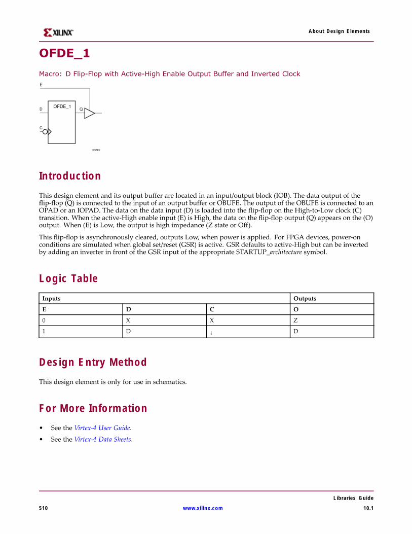
About Design Elements
OFDE_1
Macro: D Flip-Flop with Active-High Enable Output Buffer and Inverted Clock
IntroductionThis design element and its output buffer are located in an input/output block (IOB). The data output of theflip-flop (Q) is connected to the input of an output buffer or OBUFE. The output of the OBUFE is connected to anOPAD or an IOPAD. The data on the data input (D) is loaded into the flip-flop on the High-to-Low clock (C)transition. When the active-High enable input (E) is High, the data on the flip-flop output (Q) appears on the (O)output. When (E) is Low, the output is high impedance (Z state or Off).
This flip-flop is asynchronously cleared, outputs Low, when power is applied. For FPGA devices, power-onconditions are simulated when global set/reset (GSR) is active. GSR defaults to active-High but can be invertedby adding an inverter in front of the GSR input of the appropriate STARTUP_architecture symbol.
Logic TableInputs Outputs
E D C O
0 X X Z
1 D ↓ D
Design Entry MethodThis design element is only for use in schematics.
For More Information• See the Virtex-4 User Guide.
• See the Virtex-4 Data Sheets.
Libraries Guide
510 www.xilinx.com 10.1
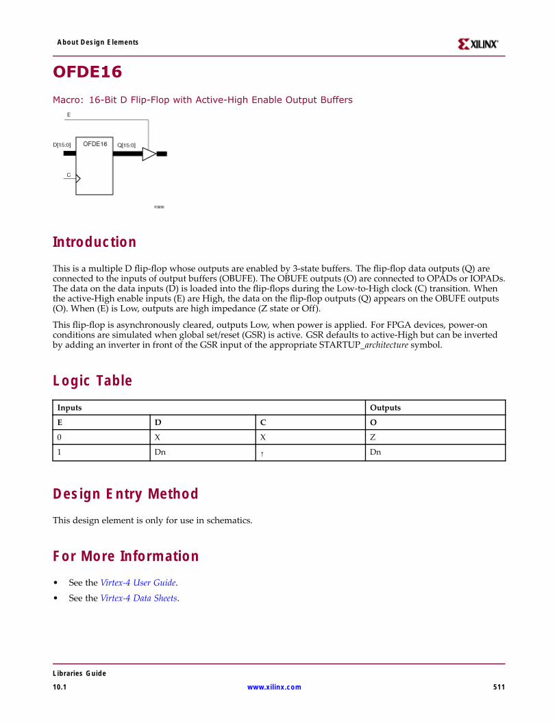
About Design Elements
OFDE16
Macro: 16-Bit D Flip-Flop with Active-High Enable Output Buffers
IntroductionThis is a multiple D flip-flop whose outputs are enabled by 3-state buffers. The flip-flop data outputs (Q) areconnected to the inputs of output buffers (OBUFE). The OBUFE outputs (O) are connected to OPADs or IOPADs.The data on the data inputs (D) is loaded into the flip-flops during the Low-to-High clock (C) transition. Whenthe active-High enable inputs (E) are High, the data on the flip-flop outputs (Q) appears on the OBUFE outputs(O). When (E) is Low, outputs are high impedance (Z state or Off).
This flip-flop is asynchronously cleared, outputs Low, when power is applied. For FPGA devices, power-onconditions are simulated when global set/reset (GSR) is active. GSR defaults to active-High but can be invertedby adding an inverter in front of the GSR input of the appropriate STARTUP_architecture symbol.
Logic TableInputs Outputs
E D C O
0 X X Z
1 Dn ↑ Dn
Design Entry MethodThis design element is only for use in schematics.
For More Information• See the Virtex-4 User Guide.
• See the Virtex-4 Data Sheets.
Libraries Guide
10.1 www.xilinx.com 511

About Design Elements
OFDE4
Macro: 4-Bit D Flip-Flop with Active-High Enable Output Buffers
IntroductionThis is a multiple D flip-flop whose outputs are enabled by 3-state buffers. The flip-flop data outputs (Q) areconnected to the inputs of output buffers (OBUFE). The OBUFE outputs (O) are connected to OPADs or IOPADs.The data on the data inputs (D) is loaded into the flip-flops during the Low-to-High clock (C) transition. Whenthe active-High enable inputs (E) are High, the data on the flip-flop outputs (Q) appears on the OBUFE outputs(O). When (E) is Low, outputs are high impedance (Z state or Off).
This flip-flop is asynchronously cleared, outputs Low, when power is applied. For FPGA devices, power-onconditions are simulated when global set/reset (GSR) is active. GSR defaults to active-High but can be invertedby adding an inverter in front of the GSR input of the appropriate STARTUP_architecture symbol.
Logic TableInputs Outputs
E D C O
0 X X Z
1 Dn ↑ Dn
Design Entry MethodThis design element is only for use in schematics.
For More Information• See the Virtex-4 User Guide.
• See the Virtex-4 Data Sheets.
Libraries Guide
512 www.xilinx.com 10.1
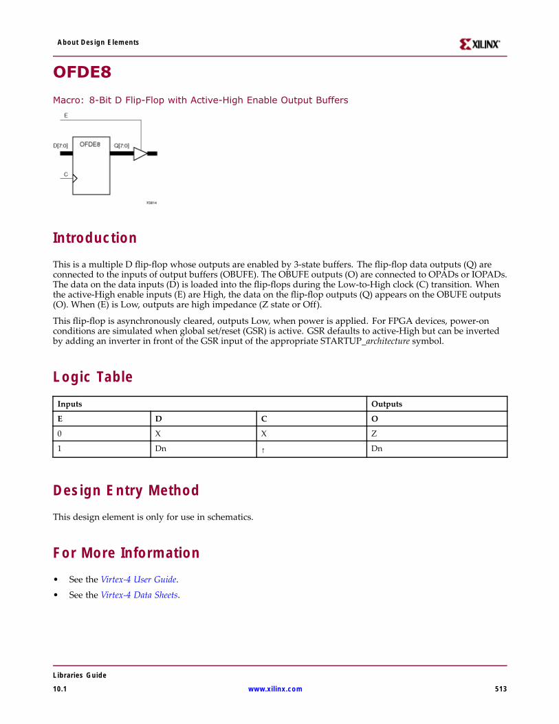
About Design Elements
OFDE8
Macro: 8-Bit D Flip-Flop with Active-High Enable Output Buffers
IntroductionThis is a multiple D flip-flop whose outputs are enabled by 3-state buffers. The flip-flop data outputs (Q) areconnected to the inputs of output buffers (OBUFE). The OBUFE outputs (O) are connected to OPADs or IOPADs.The data on the data inputs (D) is loaded into the flip-flops during the Low-to-High clock (C) transition. Whenthe active-High enable inputs (E) are High, the data on the flip-flop outputs (Q) appears on the OBUFE outputs(O). When (E) is Low, outputs are high impedance (Z state or Off).
This flip-flop is asynchronously cleared, outputs Low, when power is applied. For FPGA devices, power-onconditions are simulated when global set/reset (GSR) is active. GSR defaults to active-High but can be invertedby adding an inverter in front of the GSR input of the appropriate STARTUP_architecture symbol.
Logic TableInputs Outputs
E D C O
0 X X Z
1 Dn ↑ Dn
Design Entry MethodThis design element is only for use in schematics.
For More Information• See the Virtex-4 User Guide.
• See the Virtex-4 Data Sheets.
Libraries Guide
10.1 www.xilinx.com 513
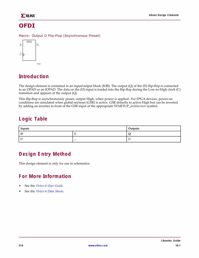
About Design Elements
OFDI
Macro: Output D Flip-Flop (Asynchronous Preset)
IntroductionThe design element is contained in an input/output block (IOB). The output (Q) of the (D) flip-flop is connectedto an OPAD or an IOPAD. The data on the (D) input is loaded into the flip-flop during the Low-to-High clock (C)transition and appears at the output (Q).
This flip-flop is asynchronously preset, output High, when power is applied. For FPGA devices, power-onconditions are simulated when global set/reset (GSR) is active. GSR defaults to active-High but can be invertedby adding an inverter in front of the GSR input of the appropriate STARTUP_architecture symbol.
Logic TableInputs Outputs
D C Q
D ↑ D
Design Entry MethodThis design element is only for use in schematics.
For More Information• See the Virtex-4 User Guide.
• See the Virtex-4 Data Sheets.
Libraries Guide
514 www.xilinx.com 10.1
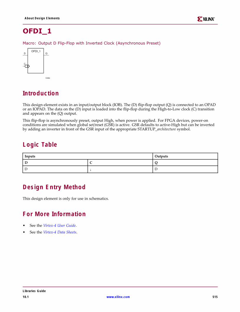
About Design Elements
OFDI_1
Macro: Output D Flip-Flop with Inverted Clock (Asynchronous Preset)
IntroductionThis design element exists in an input/output block (IOB). The (D) flip-flop output (Q) is connected to an OPADor an IOPAD. The data on the (D) input is loaded into the flip-flop during the High-to-Low clock (C) transitionand appears on the (Q) output.
This flip-flop is asynchronously preset, output High, when power is applied. For FPGA devices, power-onconditions are simulated when global set/reset (GSR) is active. GSR defaults to active-High but can be invertedby adding an inverter in front of the GSR input of the appropriate STARTUP_architecture symbol.
Logic TableInputs Outputs
D C Q
D ↓ D
Design Entry MethodThis design element is only for use in schematics.
For More Information• See the Virtex-4 User Guide.
• See the Virtex-4 Data Sheets.
Libraries Guide
10.1 www.xilinx.com 515
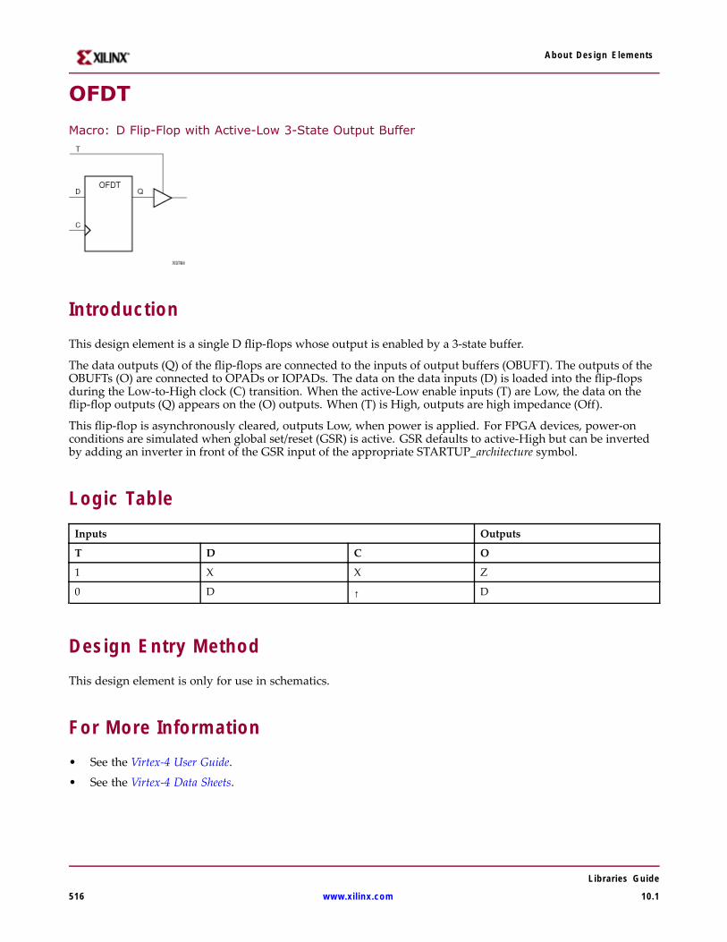
About Design Elements
OFDT
Macro: D Flip-Flop with Active-Low 3-State Output Buffer
IntroductionThis design element is a single D flip-flops whose output is enabled by a 3-state buffer.
The data outputs (Q) of the flip-flops are connected to the inputs of output buffers (OBUFT). The outputs of theOBUFTs (O) are connected to OPADs or IOPADs. The data on the data inputs (D) is loaded into the flip-flopsduring the Low-to-High clock (C) transition. When the active-Low enable inputs (T) are Low, the data on theflip-flop outputs (Q) appears on the (O) outputs. When (T) is High, outputs are high impedance (Off).
This flip-flop is asynchronously cleared, outputs Low, when power is applied. For FPGA devices, power-onconditions are simulated when global set/reset (GSR) is active. GSR defaults to active-High but can be invertedby adding an inverter in front of the GSR input of the appropriate STARTUP_architecture symbol.
Logic TableInputs Outputs
T D C O
1 X X Z
0 D ↑ D
Design Entry MethodThis design element is only for use in schematics.
For More Information• See the Virtex-4 User Guide.
• See the Virtex-4 Data Sheets.
Libraries Guide
516 www.xilinx.com 10.1

About Design Elements
OFDT_1
Macro: D Flip-Flop with Active-Low 3-State Output Buffer and Inverted Clock
IntroductionThe design element and its output buffer are located in an input/output block (IOB). The flip-flop data output(Q) is connected to the input of an output buffer (OBUFT). The OBUFT output is connected to an OPAD or anIOPAD. The data on the data input (D) is loaded into the flip-flop on the High-to-Low clock (C) transition.When the active-Low enable input (T) is Low, the data on the flip-flop output (Q) appears on the (O) output.When (T) is High, the output is high impedance (Off).
This flip-flop is asynchronously cleared, outputs Low, when power is applied. For FPGA devices, power-onconditions are simulated when global set/reset (GSR) is active. GSR defaults to active-High but can be invertedby adding an inverter in front of the GSR input of the appropriate STARTUP_architecture symbol.
Logic TableInputs Outputs
T D C O
1 X X Z
0 D ↓ D
Design Entry MethodThis design element is only for use in schematics.
For More Information• See the Virtex-4 User Guide.
• See the Virtex-4 Data Sheets.
Libraries Guide
10.1 www.xilinx.com 517
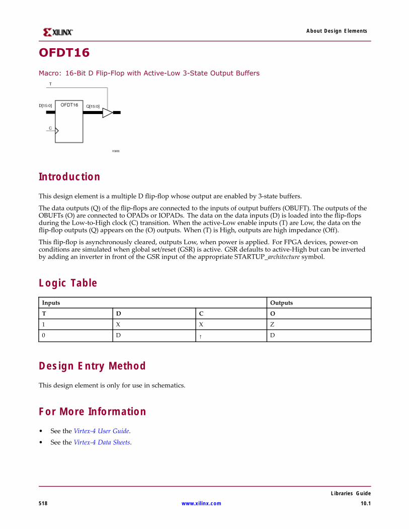
About Design Elements
OFDT16
Macro: 16-Bit D Flip-Flop with Active-Low 3-State Output Buffers
IntroductionThis design element is a multiple D flip-flop whose output are enabled by 3-state buffers.
The data outputs (Q) of the flip-flops are connected to the inputs of output buffers (OBUFT). The outputs of theOBUFTs (O) are connected to OPADs or IOPADs. The data on the data inputs (D) is loaded into the flip-flopsduring the Low-to-High clock (C) transition. When the active-Low enable inputs (T) are Low, the data on theflip-flop outputs (Q) appears on the (O) outputs. When (T) is High, outputs are high impedance (Off).
This flip-flop is asynchronously cleared, outputs Low, when power is applied. For FPGA devices, power-onconditions are simulated when global set/reset (GSR) is active. GSR defaults to active-High but can be invertedby adding an inverter in front of the GSR input of the appropriate STARTUP_architecture symbol.
Logic TableInputs Outputs
T D C O
1 X X Z
0 D ↑ D
Design Entry MethodThis design element is only for use in schematics.
For More Information• See the Virtex-4 User Guide.
• See the Virtex-4 Data Sheets.
Libraries Guide
518 www.xilinx.com 10.1
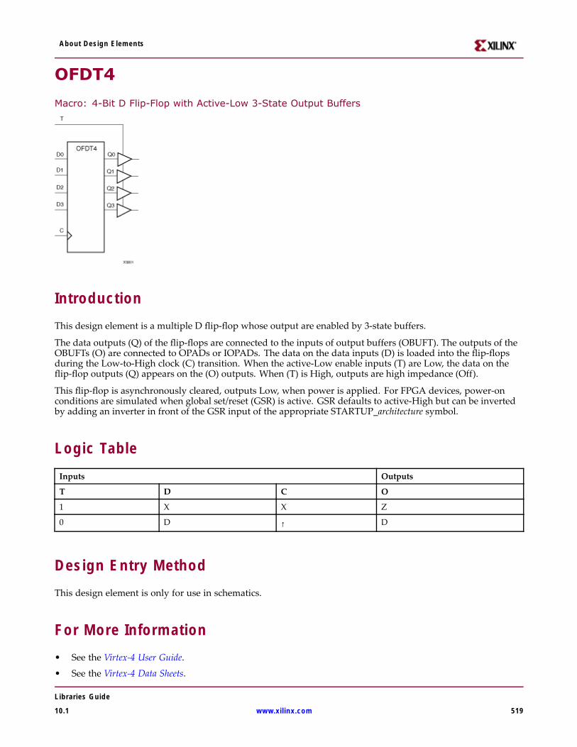
About Design Elements
OFDT4
Macro: 4-Bit D Flip-Flop with Active-Low 3-State Output Buffers
IntroductionThis design element is a multiple D flip-flop whose output are enabled by 3-state buffers.
The data outputs (Q) of the flip-flops are connected to the inputs of output buffers (OBUFT). The outputs of theOBUFTs (O) are connected to OPADs or IOPADs. The data on the data inputs (D) is loaded into the flip-flopsduring the Low-to-High clock (C) transition. When the active-Low enable inputs (T) are Low, the data on theflip-flop outputs (Q) appears on the (O) outputs. When (T) is High, outputs are high impedance (Off).
This flip-flop is asynchronously cleared, outputs Low, when power is applied. For FPGA devices, power-onconditions are simulated when global set/reset (GSR) is active. GSR defaults to active-High but can be invertedby adding an inverter in front of the GSR input of the appropriate STARTUP_architecture symbol.
Logic TableInputs Outputs
T D C O
1 X X Z
0 D ↑ D
Design Entry MethodThis design element is only for use in schematics.
For More Information• See the Virtex-4 User Guide.
• See the Virtex-4 Data Sheets.
Libraries Guide
10.1 www.xilinx.com 519
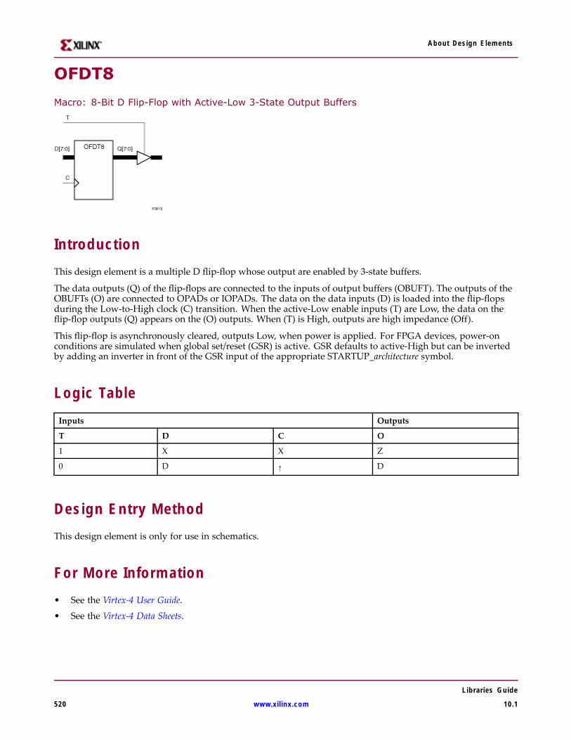
About Design Elements
OFDT8
Macro: 8-Bit D Flip-Flop with Active-Low 3-State Output Buffers
IntroductionThis design element is a multiple D flip-flop whose output are enabled by 3-state buffers.
The data outputs (Q) of the flip-flops are connected to the inputs of output buffers (OBUFT). The outputs of theOBUFTs (O) are connected to OPADs or IOPADs. The data on the data inputs (D) is loaded into the flip-flopsduring the Low-to-High clock (C) transition. When the active-Low enable inputs (T) are Low, the data on theflip-flop outputs (Q) appears on the (O) outputs. When (T) is High, outputs are high impedance (Off).
This flip-flop is asynchronously cleared, outputs Low, when power is applied. For FPGA devices, power-onconditions are simulated when global set/reset (GSR) is active. GSR defaults to active-High but can be invertedby adding an inverter in front of the GSR input of the appropriate STARTUP_architecture symbol.
Logic TableInputs Outputs
T D C O
1 X X Z
0 D ↑ D
Design Entry MethodThis design element is only for use in schematics.
For More Information• See the Virtex-4 User Guide.
• See the Virtex-4 Data Sheets.
Libraries Guide
520 www.xilinx.com 10.1
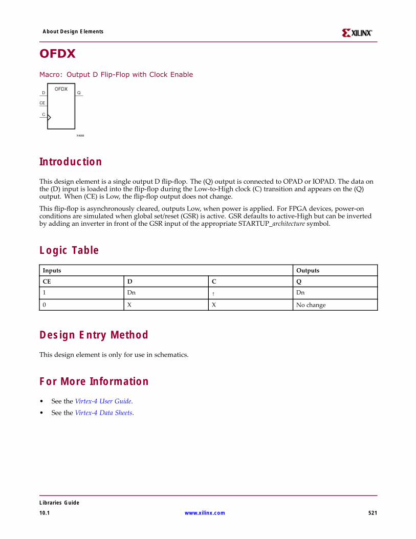
About Design Elements
OFDX
Macro: Output D Flip-Flop with Clock Enable
IntroductionThis design element is a single output D flip-flop. The (Q) output is connected to OPAD or IOPAD. The data onthe (D) input is loaded into the flip-flop during the Low-to-High clock (C) transition and appears on the (Q)output. When (CE) is Low, the flip-flop output does not change.
This flip-flop is asynchronously cleared, outputs Low, when power is applied. For FPGA devices, power-onconditions are simulated when global set/reset (GSR) is active. GSR defaults to active-High but can be invertedby adding an inverter in front of the GSR input of the appropriate STARTUP_architecture symbol.
Logic TableInputs Outputs
CE D C Q
1 Dn ↑ Dn
0 X X No change
Design Entry MethodThis design element is only for use in schematics.
For More Information• See the Virtex-4 User Guide.
• See the Virtex-4 Data Sheets.
Libraries Guide
10.1 www.xilinx.com 521

About Design Elements
OFDX_1
Macro: Output D Flip-Flop with Inverted Clock and Clock Enable
IntroductionThe design element is located in an input/output block (IOB). The output (Q) of the (D) flip-flop is connected toan OPAD or an IOPAD. The data on the (D) input is loaded into the flip-flop during the High-to-Low clock (C)transition and appears on the (Q) output. When the (CE) pin is Low, the output (Q) does not change.
This flip-flop is asynchronously cleared, outputs Low, when power is applied. For FPGA devices, power-onconditions are simulated when global set/reset (GSR) is active. GSR defaults to active-High but can be invertedby adding an inverter in front of the GSR input of the appropriate STARTUP_architecture symbol.
Logic TableInputs Outputs
CE D C Q
1 D ↓ D
0 X X No Change
Design Entry MethodThis design element is only for use in schematics.
For More Information• See the Virtex-4 User Guide.
• See the Virtex-4 Data Sheets.
Libraries Guide
522 www.xilinx.com 10.1
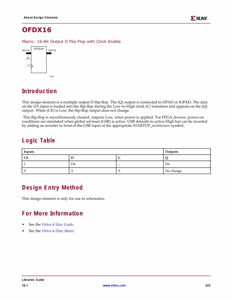
About Design Elements
OFDX16
Macro: 16-Bit Output D Flip-Flop with Clock Enable
IntroductionThis design element is a multiple output D flip-flop. The (Q) output is connected to OPAD or IOPAD. The dataon the (D) input is loaded into the flip-flop during the Low-to-High clock (C) transition and appears on the (Q)output. When (CE) is Low, the flip-flop output does not change.
This flip-flop is asynchronously cleared, outputs Low, when power is applied. For FPGA devices, power-onconditions are simulated when global set/reset (GSR) is active. GSR defaults to active-High but can be invertedby adding an inverter in front of the GSR input of the appropriate STARTUP_architecture symbol.
Logic TableInputs Outputs
CE D C Q
1 Dn ↑ Dn
0 X X No change
Design Entry MethodThis design element is only for use in schematics.
For More Information• See the Virtex-4 User Guide.
• See the Virtex-4 Data Sheets.
Libraries Guide
10.1 www.xilinx.com 523
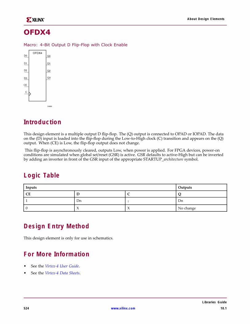
About Design Elements
OFDX4
Macro: 4-Bit Output D Flip-Flop with Clock Enable
IntroductionThis design element is a multiple output D flip-flop. The (Q) output is connected to OPAD or IOPAD. The dataon the (D) input is loaded into the flip-flop during the Low-to-High clock (C) transition and appears on the (Q)output. When (CE) is Low, the flip-flop output does not change.
This flip-flop is asynchronously cleared, outputs Low, when power is applied. For FPGA devices, power-onconditions are simulated when global set/reset (GSR) is active. GSR defaults to active-High but can be invertedby adding an inverter in front of the GSR input of the appropriate STARTUP_architecture symbol.
Logic TableInputs Outputs
CE D C Q
1 Dn ↑ Dn
0 X X No change
Design Entry MethodThis design element is only for use in schematics.
For More Information• See the Virtex-4 User Guide.
• See the Virtex-4 Data Sheets.
Libraries Guide
524 www.xilinx.com 10.1
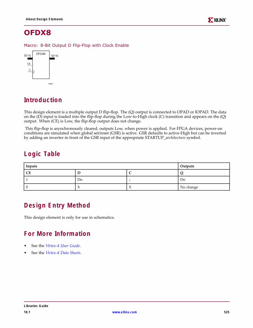
About Design Elements
OFDX8
Macro: 8-Bit Output D Flip-Flop with Clock Enable
IntroductionThis design element is a multiple output D flip-flop. The (Q) output is connected to OPAD or IOPAD. The dataon the (D) input is loaded into the flip-flop during the Low-to-High clock (C) transition and appears on the (Q)output. When (CE) is Low, the flip-flop output does not change.
This flip-flop is asynchronously cleared, outputs Low, when power is applied. For FPGA devices, power-onconditions are simulated when global set/reset (GSR) is active. GSR defaults to active-High but can be invertedby adding an inverter in front of the GSR input of the appropriate STARTUP_architecture symbol.
Logic TableInputs Outputs
CE D C Q
1 Dn ↑ Dn
0 X X No change
Design Entry MethodThis design element is only for use in schematics.
For More Information• See the Virtex-4 User Guide.
• See the Virtex-4 Data Sheets.
Libraries Guide
10.1 www.xilinx.com 525
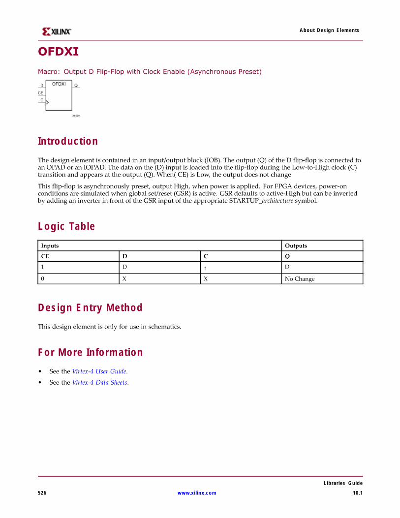
About Design Elements
OFDXI
Macro: Output D Flip-Flop with Clock Enable (Asynchronous Preset)
IntroductionThe design element is contained in an input/output block (IOB). The output (Q) of the D flip-flop is connected toan OPAD or an IOPAD. The data on the (D) input is loaded into the flip-flop during the Low-to-High clock (C)transition and appears at the output (Q). When( CE) is Low, the output does not change
This flip-flop is asynchronously preset, output High, when power is applied. For FPGA devices, power-onconditions are simulated when global set/reset (GSR) is active. GSR defaults to active-High but can be invertedby adding an inverter in front of the GSR input of the appropriate STARTUP_architecture symbol.
Logic TableInputs Outputs
CE D C Q
1 D ↑ D
0 X X No Change
Design Entry MethodThis design element is only for use in schematics.
For More Information• See the Virtex-4 User Guide.
• See the Virtex-4 Data Sheets.
Libraries Guide
526 www.xilinx.com 10.1
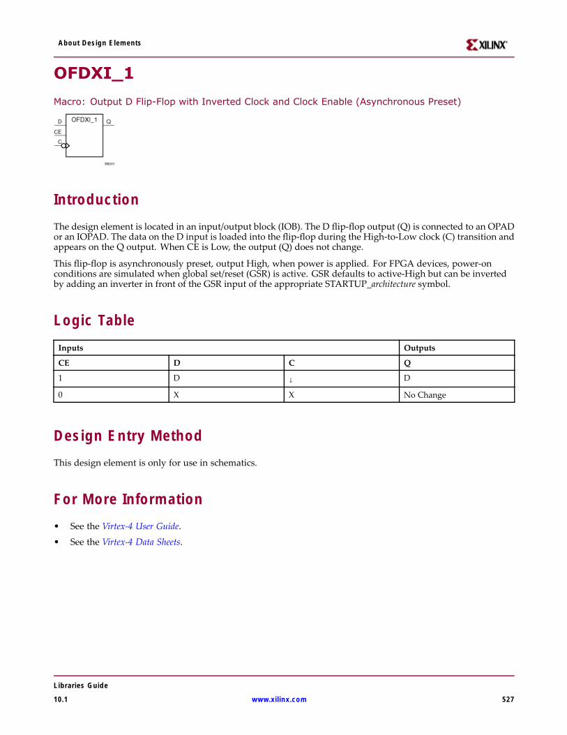
About Design Elements
OFDXI_1
Macro: Output D Flip-Flop with Inverted Clock and Clock Enable (Asynchronous Preset)
IntroductionThe design element is located in an input/output block (IOB). The D flip-flop output (Q) is connected to an OPADor an IOPAD. The data on the D input is loaded into the flip-flop during the High-to-Low clock (C) transition andappears on the Q output. When CE is Low, the output (Q) does not change.
This flip-flop is asynchronously preset, output High, when power is applied. For FPGA devices, power-onconditions are simulated when global set/reset (GSR) is active. GSR defaults to active-High but can be invertedby adding an inverter in front of the GSR input of the appropriate STARTUP_architecture symbol.
Logic TableInputs Outputs
CE D C Q
1 D ↓ D
0 X X No Change
Design Entry MethodThis design element is only for use in schematics.
For More Information• See the Virtex-4 User Guide.
• See the Virtex-4 Data Sheets.
Libraries Guide
10.1 www.xilinx.com 527
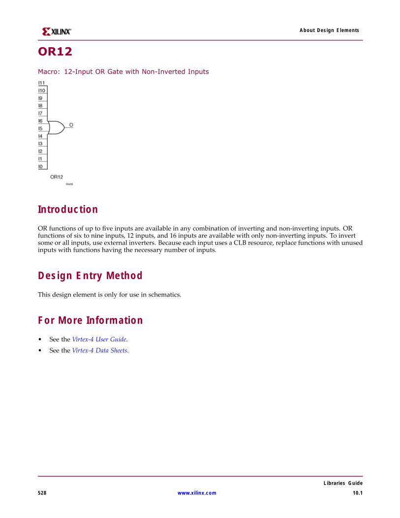
About Design Elements
OR12
Macro: 12-Input OR Gate with Non-Inverted Inputs
IntroductionOR functions of up to five inputs are available in any combination of inverting and non-inverting inputs. ORfunctions of six to nine inputs, 12 inputs, and 16 inputs are available with only non-inverting inputs. To invertsome or all inputs, use external inverters. Because each input uses a CLB resource, replace functions with unusedinputs with functions having the necessary number of inputs.
Design Entry MethodThis design element is only for use in schematics.
For More Information• See the Virtex-4 User Guide.
• See the Virtex-4 Data Sheets.
Libraries Guide
528 www.xilinx.com 10.1
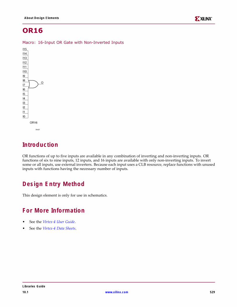
About Design Elements
OR16
Macro: 16-Input OR Gate with Non-Inverted Inputs
IntroductionOR functions of up to five inputs are available in any combination of inverting and non-inverting inputs. ORfunctions of six to nine inputs, 12 inputs, and 16 inputs are available with only non-inverting inputs. To invertsome or all inputs, use external inverters. Because each input uses a CLB resource, replace functions with unusedinputs with functions having the necessary number of inputs.
Design Entry MethodThis design element is only for use in schematics.
For More Information• See the Virtex-4 User Guide.
• See the Virtex-4 Data Sheets.
Libraries Guide
10.1 www.xilinx.com 529

About Design Elements
OR2
Primitive: 2-Input OR Gate with Non-Inverted Inputs
IntroductionOR functions of up to five inputs are available in any combination of inverting and non-inverting inputs. ORfunctions of six to nine inputs, 12 inputs, and 16 inputs are available with only non-inverting inputs. To invertsome or all inputs, use external inverters. Because each input uses a CLB resource, replace functions with unusedinputs with functions having the necessary number of inputs.
Design Entry MethodThis design element is only for use in schematics.
For More Information• See the Virtex-4 User Guide.
• See the Virtex-4 Data Sheets.
Libraries Guide
530 www.xilinx.com 10.1

About Design Elements
OR2B1
Primitive: 2-Input OR Gate with 1 Inverted and 1 Non-Inverted Inputs
IntroductionOR functions of up to five inputs are available in any combination of inverting and non-inverting inputs. ORfunctions of six to nine inputs, 12 inputs, and 16 inputs are available with only non-inverting inputs. To invertsome or all inputs, use external inverters. Because each input uses a CLB resource, replace functions with unusedinputs with functions having the necessary number of inputs.
Design Entry MethodThis design element is only for use in schematics.
For More Information• See the Virtex-4 User Guide.
• See the Virtex-4 Data Sheets.
Libraries Guide
10.1 www.xilinx.com 531
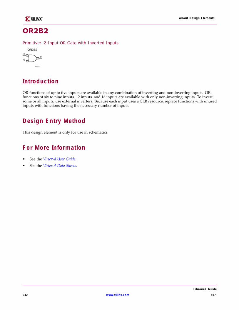
About Design Elements
OR2B2
Primitive: 2-Input OR Gate with Inverted Inputs
IntroductionOR functions of up to five inputs are available in any combination of inverting and non-inverting inputs. ORfunctions of six to nine inputs, 12 inputs, and 16 inputs are available with only non-inverting inputs. To invertsome or all inputs, use external inverters. Because each input uses a CLB resource, replace functions with unusedinputs with functions having the necessary number of inputs.
Design Entry MethodThis design element is only for use in schematics.
For More Information• See the Virtex-4 User Guide.
• See the Virtex-4 Data Sheets.
Libraries Guide
532 www.xilinx.com 10.1
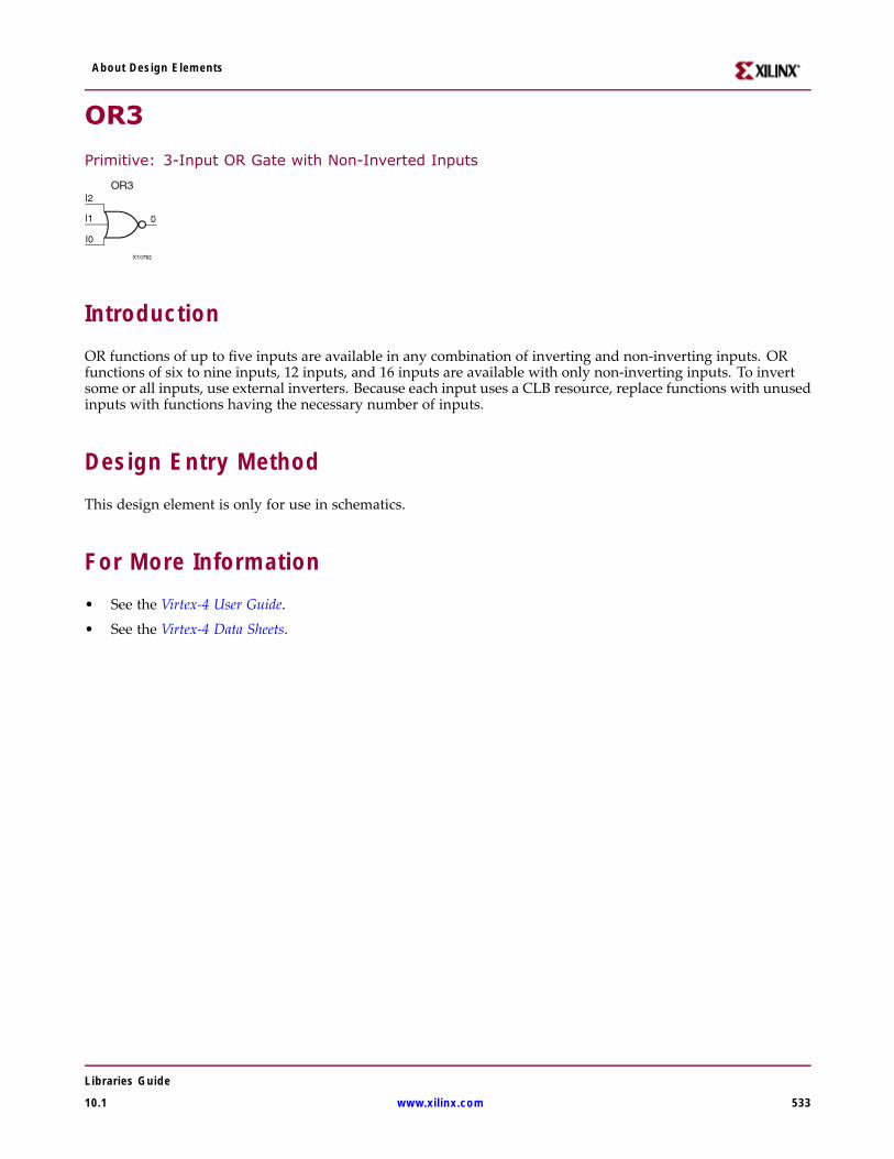
About Design Elements
OR3
Primitive: 3-Input OR Gate with Non-Inverted Inputs
IntroductionOR functions of up to five inputs are available in any combination of inverting and non-inverting inputs. ORfunctions of six to nine inputs, 12 inputs, and 16 inputs are available with only non-inverting inputs. To invertsome or all inputs, use external inverters. Because each input uses a CLB resource, replace functions with unusedinputs with functions having the necessary number of inputs.
Design Entry MethodThis design element is only for use in schematics.
For More Information• See the Virtex-4 User Guide.
• See the Virtex-4 Data Sheets.
Libraries Guide
10.1 www.xilinx.com 533
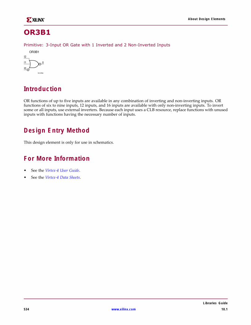
About Design Elements
OR3B1
Primitive: 3-Input OR Gate with 1 Inverted and 2 Non-Inverted Inputs
IntroductionOR functions of up to five inputs are available in any combination of inverting and non-inverting inputs. ORfunctions of six to nine inputs, 12 inputs, and 16 inputs are available with only non-inverting inputs. To invertsome or all inputs, use external inverters. Because each input uses a CLB resource, replace functions with unusedinputs with functions having the necessary number of inputs.
Design Entry MethodThis design element is only for use in schematics.
For More Information• See the Virtex-4 User Guide.
• See the Virtex-4 Data Sheets.
Libraries Guide
534 www.xilinx.com 10.1

About Design Elements
OR3B2
Primitive: 3-Input OR Gate with 2 Inverted and 1 Non-Inverted Inputs
IntroductionOR functions of up to five inputs are available in any combination of inverting and non-inverting inputs. ORfunctions of six to nine inputs, 12 inputs, and 16 inputs are available with only non-inverting inputs. To invertsome or all inputs, use external inverters. Because each input uses a CLB resource, replace functions with unusedinputs with functions having the necessary number of inputs.
Design Entry MethodThis design element is only for use in schematics.
For More Information• See the Virtex-4 User Guide.
• See the Virtex-4 Data Sheets.
Libraries Guide
10.1 www.xilinx.com 535

About Design Elements
OR3B3
Primitive: 3-Input OR Gate with Inverted Inputs
IntroductionOR functions of up to five inputs are available in any combination of inverting and non-inverting inputs. ORfunctions of six to nine inputs, 12 inputs, and 16 inputs are available with only non-inverting inputs. To invertsome or all inputs, use external inverters. Because each input uses a CLB resource, replace functions with unusedinputs with functions having the necessary number of inputs.
Design Entry MethodThis design element is only for use in schematics.
For More Information• See the Virtex-4 User Guide.
• See the Virtex-4 Data Sheets.
Libraries Guide
536 www.xilinx.com 10.1
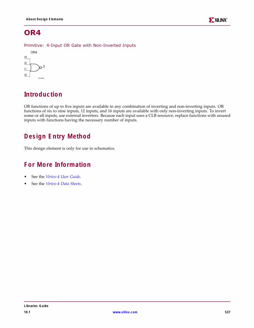
About Design Elements
OR4
Primitive: 4-Input OR Gate with Non-Inverted Inputs
IntroductionOR functions of up to five inputs are available in any combination of inverting and non-inverting inputs. ORfunctions of six to nine inputs, 12 inputs, and 16 inputs are available with only non-inverting inputs. To invertsome or all inputs, use external inverters. Because each input uses a CLB resource, replace functions with unusedinputs with functions having the necessary number of inputs.
Design Entry MethodThis design element is only for use in schematics.
For More Information• See the Virtex-4 User Guide.
• See the Virtex-4 Data Sheets.
Libraries Guide
10.1 www.xilinx.com 537

About Design Elements
OR4B1
Primitive: 4-Input OR Gate with 1 Inverted and 3 Non-Inverted Inputs
IntroductionOR functions of up to five inputs are available in any combination of inverting and non-inverting inputs. ORfunctions of six to nine inputs, 12 inputs, and 16 inputs are available with only non-inverting inputs. To invertsome or all inputs, use external inverters. Because each input uses a CLB resource, replace functions with unusedinputs with functions having the necessary number of inputs.
Design Entry MethodThis design element is only for use in schematics.
For More Information• See the Virtex-4 User Guide.
• See the Virtex-4 Data Sheets.
Libraries Guide
538 www.xilinx.com 10.1

About Design Elements
OR4B2
Primitive: 4-Input OR Gate with 2 Inverted and 2 Non-Inverted Inputs
IntroductionOR functions of up to five inputs are available in any combination of inverting and non-inverting inputs. ORfunctions of six to nine inputs, 12 inputs, and 16 inputs are available with only non-inverting inputs. To invertsome or all inputs, use external inverters. Because each input uses a CLB resource, replace functions with unusedinputs with functions having the necessary number of inputs.
Design Entry MethodThis design element is only for use in schematics.
For More Information• See the Virtex-4 User Guide.
• See the Virtex-4 Data Sheets.
Libraries Guide
10.1 www.xilinx.com 539

About Design Elements
OR4B3
Primitive: 4-Input OR Gate with 3 Inverted and 1 Non-Inverted Inputs
IntroductionOR functions of up to five inputs are available in any combination of inverting and non-inverting inputs. ORfunctions of six to nine inputs, 12 inputs, and 16 inputs are available with only non-inverting inputs. To invertsome or all inputs, use external inverters. Because each input uses a CLB resource, replace functions with unusedinputs with functions having the necessary number of inputs.
Design Entry MethodThis design element is only for use in schematics.
For More Information• See the Virtex-4 User Guide.
• See the Virtex-4 Data Sheets.
Libraries Guide
540 www.xilinx.com 10.1
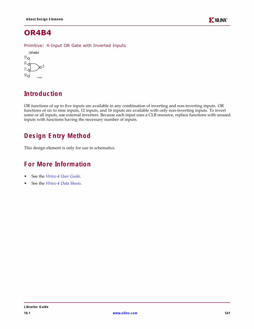
About Design Elements
OR4B4
Primitive: 4-Input OR Gate with Inverted Inputs
IntroductionOR functions of up to five inputs are available in any combination of inverting and non-inverting inputs. ORfunctions of six to nine inputs, 12 inputs, and 16 inputs are available with only non-inverting inputs. To invertsome or all inputs, use external inverters. Because each input uses a CLB resource, replace functions with unusedinputs with functions having the necessary number of inputs.
Design Entry MethodThis design element is only for use in schematics.
For More Information• See the Virtex-4 User Guide.
• See the Virtex-4 Data Sheets.
Libraries Guide
10.1 www.xilinx.com 541

About Design Elements
OR5
Primitive: 5-Input OR Gate with Non-Inverted Inputs
IntroductionOR functions of up to five inputs are available in any combination of inverting and non-inverting inputs. ORfunctions of six to nine inputs, 12 inputs, and 16 inputs are available with only non-inverting inputs. To invertsome or all inputs, use external inverters. Because each input uses a CLB resource, replace functions with unusedinputs with functions having the necessary number of inputs.
Design Entry MethodThis design element is only for use in schematics.
For More Information• See the Virtex-4 User Guide.
• See the Virtex-4 Data Sheets.
Libraries Guide
542 www.xilinx.com 10.1

About Design Elements
OR5B1
Primitive: 5-Input OR Gate with 1 Inverted and 4 Non-Inverted Inputs
IntroductionOR functions of up to five inputs are available in any combination of inverting and non-inverting inputs. ORfunctions of six to nine inputs, 12 inputs, and 16 inputs are available with only non-inverting inputs. To invertsome or all inputs, use external inverters. Because each input uses a CLB resource, replace functions with unusedinputs with functions having the necessary number of inputs.
Design Entry MethodThis design element is only for use in schematics.
For More Information• See the Virtex-4 User Guide.
• See the Virtex-4 Data Sheets.
Libraries Guide
10.1 www.xilinx.com 543
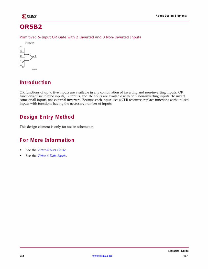
About Design Elements
OR5B2
Primitive: 5-Input OR Gate with 2 Inverted and 3 Non-Inverted Inputs
IntroductionOR functions of up to five inputs are available in any combination of inverting and non-inverting inputs. ORfunctions of six to nine inputs, 12 inputs, and 16 inputs are available with only non-inverting inputs. To invertsome or all inputs, use external inverters. Because each input uses a CLB resource, replace functions with unusedinputs with functions having the necessary number of inputs.
Design Entry MethodThis design element is only for use in schematics.
For More Information• See the Virtex-4 User Guide.
• See the Virtex-4 Data Sheets.
Libraries Guide
544 www.xilinx.com 10.1

About Design Elements
OR5B3
Primitive: 5-Input OR Gate with 3 Inverted and 2 Non-Inverted Inputs
IntroductionOR functions of up to five inputs are available in any combination of inverting and non-inverting inputs. ORfunctions of six to nine inputs, 12 inputs, and 16 inputs are available with only non-inverting inputs. To invertsome or all inputs, use external inverters. Because each input uses a CLB resource, replace functions with unusedinputs with functions having the necessary number of inputs.
Design Entry MethodThis design element is only for use in schematics.
For More Information• See the Virtex-4 User Guide.
• See the Virtex-4 Data Sheets.
Libraries Guide
10.1 www.xilinx.com 545

About Design Elements
OR5B4
Primitive: 5-Input OR Gate with 4 Inverted and 1 Non-Inverted Inputs
IntroductionOR functions of up to five inputs are available in any combination of inverting and non-inverting inputs. ORfunctions of six to nine inputs, 12 inputs, and 16 inputs are available with only non-inverting inputs. To invertsome or all inputs, use external inverters. Because each input uses a CLB resource, replace functions with unusedinputs with functions having the necessary number of inputs.
Design Entry MethodThis design element is only for use in schematics.
For More Information• See the Virtex-4 User Guide.
• See the Virtex-4 Data Sheets.
Libraries Guide
546 www.xilinx.com 10.1

About Design Elements
OR5B5
Primitive: 5-Input OR Gate with Inverted Inputs
IntroductionOR functions of up to five inputs are available in any combination of inverting and non-inverting inputs. ORfunctions of six to nine inputs, 12 inputs, and 16 inputs are available with only non-inverting inputs. To invertsome or all inputs, use external inverters. Because each input uses a CLB resource, replace functions with unusedinputs with functions having the necessary number of inputs.
Design Entry MethodThis design element is only for use in schematics.
For More Information• See the Virtex-4 User Guide.
• See the Virtex-4 Data Sheets.
Libraries Guide
10.1 www.xilinx.com 547
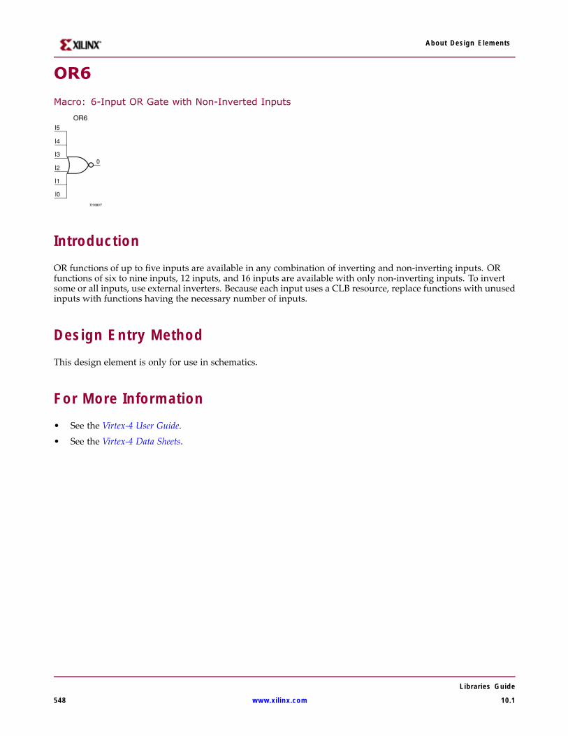
About Design Elements
OR6
Macro: 6-Input OR Gate with Non-Inverted Inputs
IntroductionOR functions of up to five inputs are available in any combination of inverting and non-inverting inputs. ORfunctions of six to nine inputs, 12 inputs, and 16 inputs are available with only non-inverting inputs. To invertsome or all inputs, use external inverters. Because each input uses a CLB resource, replace functions with unusedinputs with functions having the necessary number of inputs.
Design Entry MethodThis design element is only for use in schematics.
For More Information• See the Virtex-4 User Guide.
• See the Virtex-4 Data Sheets.
Libraries Guide
548 www.xilinx.com 10.1
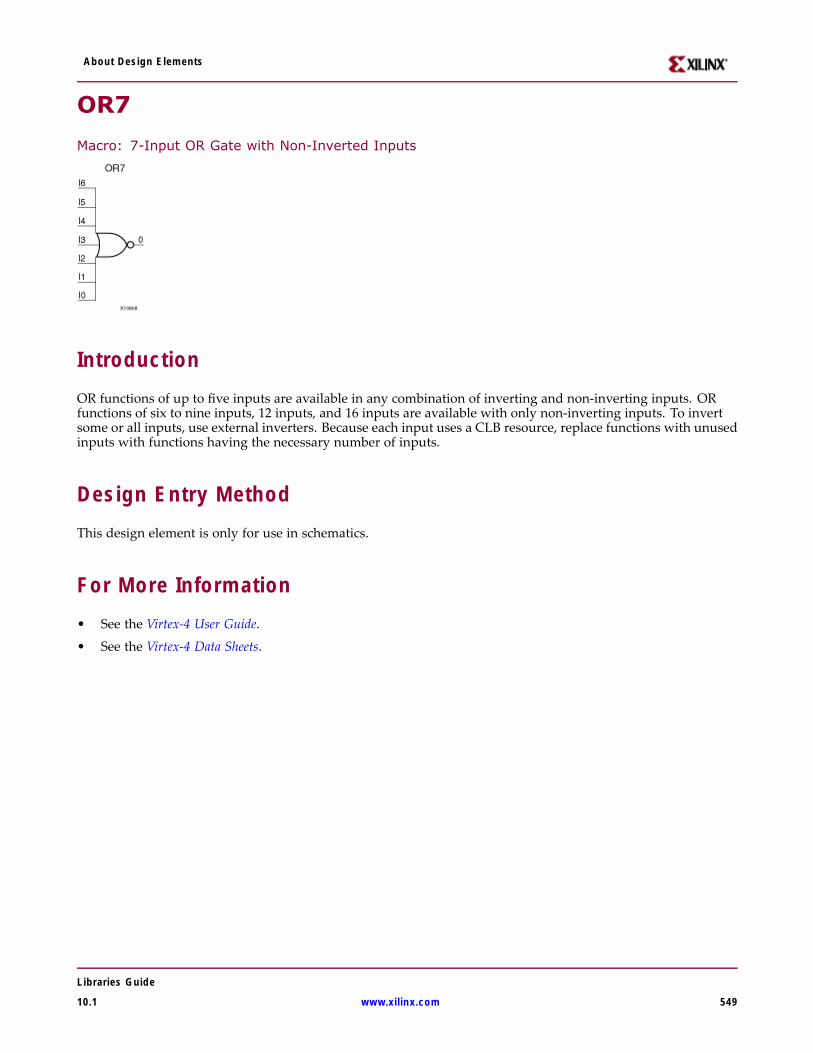
About Design Elements
OR7
Macro: 7-Input OR Gate with Non-Inverted Inputs
IntroductionOR functions of up to five inputs are available in any combination of inverting and non-inverting inputs. ORfunctions of six to nine inputs, 12 inputs, and 16 inputs are available with only non-inverting inputs. To invertsome or all inputs, use external inverters. Because each input uses a CLB resource, replace functions with unusedinputs with functions having the necessary number of inputs.
Design Entry MethodThis design element is only for use in schematics.
For More Information• See the Virtex-4 User Guide.
• See the Virtex-4 Data Sheets.
Libraries Guide
10.1 www.xilinx.com 549

About Design Elements
OR8
Macro: 8-Input OR Gate with Non-Inverted Inputs
IntroductionOR functions of up to five inputs are available in any combination of inverting and non-inverting inputs. ORfunctions of six to nine inputs, 12 inputs, and 16 inputs are available with only non-inverting inputs. To invertsome or all inputs, use external inverters. Because each input uses a CLB resource, replace functions with unusedinputs with functions having the necessary number of inputs.
Design Entry MethodThis design element is only for use in schematics.
For More Information• See the Virtex-4 User Guide.
• See the Virtex-4 Data Sheets.
Libraries Guide
550 www.xilinx.com 10.1
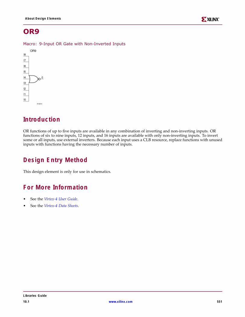
About Design Elements
OR9
Macro: 9-Input OR Gate with Non-Inverted Inputs
IntroductionOR functions of up to five inputs are available in any combination of inverting and non-inverting inputs. ORfunctions of six to nine inputs, 12 inputs, and 16 inputs are available with only non-inverting inputs. To invertsome or all inputs, use external inverters. Because each input uses a CLB resource, replace functions with unusedinputs with functions having the necessary number of inputs.
Design Entry MethodThis design element is only for use in schematics.
For More Information• See the Virtex-4 User Guide.
• See the Virtex-4 Data Sheets.
Libraries Guide
10.1 www.xilinx.com 551
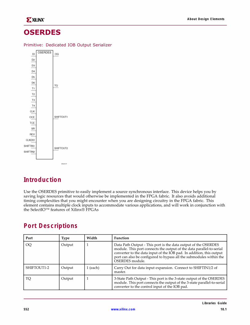
About Design Elements
OSERDES
Primitive: Dedicated IOB Output Serializer
IntroductionUse the OSERDES primitive to easily implement a source synchronous interface. This device helps you bysaving logic resources that would otherwise be implemented in the FPGA fabric. It also avoids additionaltiming complexities that you might encounter when you are designing circuitry in the FPGA fabric. Thiselement contains multiple clock inputs to accommodate various applications, and will work in conjunction withthe SelectIO™ features of Xilinx® FPGAs
Port DescriptionsPort Type Width Function
OQ Output 1 Data Path Output - This port is the data output of the OSERDESmodule. This port connects the output of the data parallel-to-serialconverter to the data input of the IOB pad. In addition, this outputport can also be configured to bypass all the submodules within theOSERDES module.
SHIFTOUT1-2 Output 1 (each) Carry Out for data input expansion. Connect to SHIFTIN1/2 ofmaster.
TQ Output 1 3-State Path Output - This port is the 3-state output of the OSERDESmodule. This port connects the output of the 3-state parallel-to-serialconverter to the control input of the IOB pad.
Libraries Guide
552 www.xilinx.com 10.1
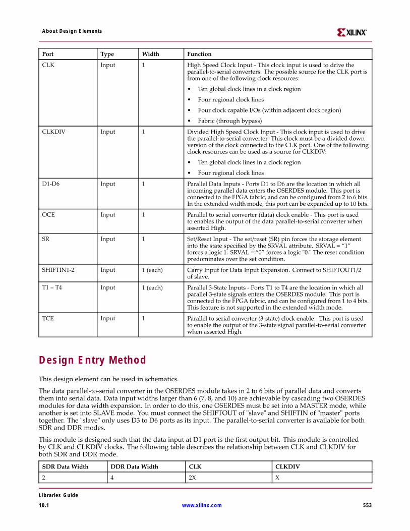
About Design Elements
Port Type Width Function
CLK Input 1 High Speed Clock Input - This clock input is used to drive theparallel-to-serial converters. The possible source for the CLK port isfrom one of the following clock resources:
• Ten global clock lines in a clock region
• Four regional clock lines
• Four clock capable I/Os (within adjacent clock region)
• Fabric (through bypass)
CLKDIV Input 1 Divided High Speed Clock Input - This clock input is used to drivethe parallel-to-serial converter. This clock must be a divided downversion of the clock connected to the CLK port. One of the followingclock resources can be used as a source for CLKDIV:
• Ten global clock lines in a clock region
• Four regional clock lines
D1-D6 Input 1 Parallel Data Inputs - Ports D1 to D6 are the location in which allincoming parallel data enters the OSERDES module. This port isconnected to the FPGA fabric, and can be configured from 2 to 6 bits.In the extended width mode, this port can be expanded up to 10 bits.
OCE Input 1 Parallel to serial converter (data) clock enable - This port is usedto enables the output of the data parallel-to-serial converter whenasserted High.
SR Input 1 Set/Reset Input - The set/reset (SR) pin forces the storage elementinto the state specified by the SRVAL attribute. SRVAL = “1”forces a logic 1. SRVAL = “0” forces a logic "0." The reset conditionpredominates over the set condition.
SHIFTIN1-2 Input 1 (each) Carry Input for Data Input Expansion. Connect to SHIFTOUT1/2of slave.
T1 – T4 Input 1 (each) Parallel 3-State Inputs - Ports T1 to T4 are the location in which allparallel 3-state signals enters the OSERDES module. This port isconnected to the FPGA fabric, and can be configured from 1 to 4 bits.This feature is not supported in the extended width mode.
TCE Input 1 Parallel to serial converter (3-state) clock enable - This port is usedto enable the output of the 3-state signal parallel-to-serial converterwhen asserted High.
Design Entry MethodThis design element can be used in schematics.
The data parallel-to-serial converter in the OSERDES module takes in 2 to 6 bits of parallel data and convertsthem into serial data. Data input widths larger than 6 (7, 8, and 10) are achievable by cascading two OSERDESmodules for data width expansion. In order to do this, one OSERDES must be set into a MASTER mode, whileanother is set into SLAVE mode. You must connect the SHIFTOUT of "slave" and SHIFTIN of "master" portstogether. The "slave" only uses D3 to D6 ports as its input. The parallel-to-serial converter is available for bothSDR and DDR modes.
This module is designed such that the data input at D1 port is the first output bit. This module is controlledby CLK and CLKDIV clocks. The following table describes the relationship between CLK and CLKDIV forboth SDR and DDR mode.
SDR Data Width DDR Data Width CLK CLKDIV
2 4 2X X
Libraries Guide
10.1 www.xilinx.com 553

About Design Elements
SDR Data Width DDR Data Width CLK CLKDIV
3 6 3X X
4 8 4X X
5 10 5X X
6 - 6X X
7 - 7X X
8 - 8X X
Output of this block is connected to the data input of an IOB pad of the FPGA. This IOB pad can be configured toa desired standard using SelectIO.
Parallel-to-Serial Converter (3-state)
The 3-state parallel-to-serial converter in the OSERDES module takes in up to 4 bits of parallel 3-state signals andconverts them into serial 3-state signal. Unlike the data parallel-to-serial converter, the 3-state parallel-to-serialconverter is not extendable to more than 4-bit, 3-state signals. This module is primarily controlled by CLK andCLKDIV clocks. In order to use this module, the following attributes must be declared: DATA_RATE_TQ andTRISTATE_WIDTH. In certain cases, you can also need to declare DATA_RATE_OQ and DATA_WIDTH. Thefollowing table lists the attributes needed for the desired functionality.
Mode of Operation DATA_RATE_TQ TRISTATE_WIDTH
4-bit DDR* DDR 4
1-bit SDR SDR 1
Buffer BUF 1
Output of this block is connected to the 3-state input of an IOB pad of the FPGA. This IOB pad can be configuredto a desired standard using SelectIO.
Width Expansion
It is possible to use this element to transmit parallel data widths larger than six. However, the 3-state output isnot expandable. In order to use this feature, two of these elements need to be instantiated, and the two must be anadjacent master and slave pair. The attribute MODE must be set to either "MASTER" or "SLAVE" in order todifferentiate the modes of the OSERDES pair. In addition, you must connect the SHIFTIN ports of the MASTERto the SHIFTOUT ports of the SLAVE. This feature supports data widths of 7, 8, and 10 for SDR and DDR mode.The table below lists the data width availability for SDR and DDR mode.
Mode Widths
SDR Data Widths 2,3,4,5,6,7,8
DDR Data Widths 4,6,8,10
Available AttributesAttribute Type Allowed Values Default Description
DATA_RATE_OQ String "SDR" or "DDR" "DDR" Defines whether the data changes at everyclock edge or every positive clock edgewith respect to CLK.
DATA_RATE_TQ String "BUF", "SDR","DDR"
"DDR" Defines whether the 3-state changes atevery clock edge, every positive clockedge, or buffer configuration with respectto CLK.
Libraries Guide
554 www.xilinx.com 10.1
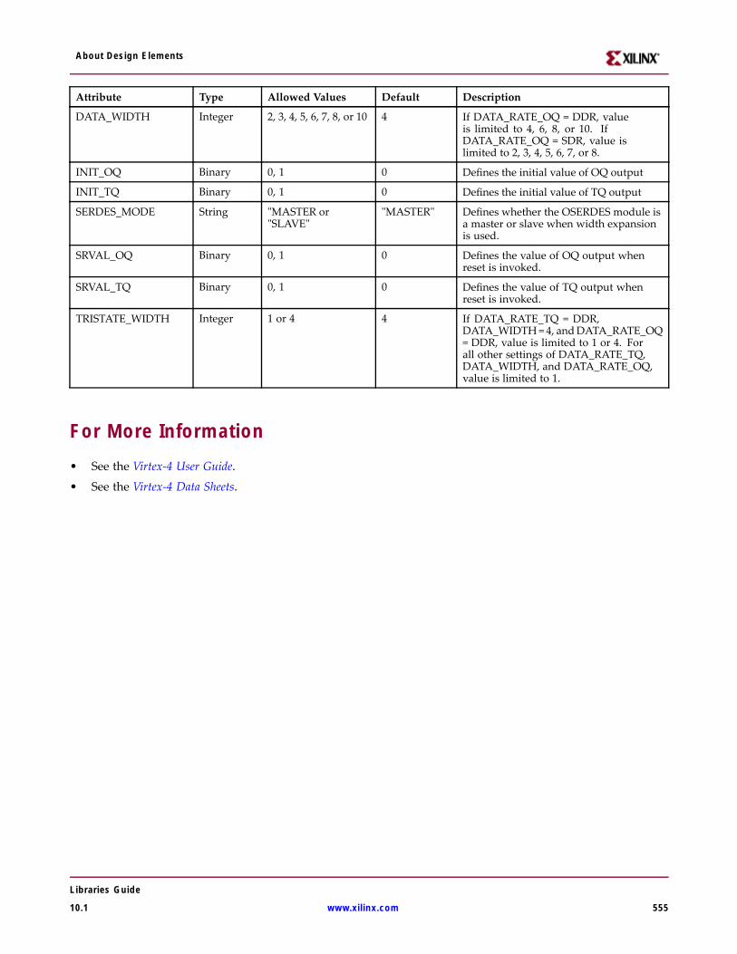
About Design Elements
Attribute Type Allowed Values Default Description
DATA_WIDTH Integer 2, 3, 4, 5, 6, 7, 8, or 10 4 If DATA_RATE_OQ = DDR, valueis limited to 4, 6, 8, or 10. IfDATA_RATE_OQ = SDR, value islimited to 2, 3, 4, 5, 6, 7, or 8.
INIT_OQ Binary 0, 1 0 Defines the initial value of OQ output
INIT_TQ Binary 0, 1 0 Defines the initial value of TQ output
SERDES_MODE String "MASTER or"SLAVE"
"MASTER" Defines whether the OSERDES module isa master or slave when width expansionis used.
SRVAL_OQ Binary 0, 1 0 Defines the value of OQ output whenreset is invoked.
SRVAL_TQ Binary 0, 1 0 Defines the value of TQ output whenreset is invoked.
TRISTATE_WIDTH Integer 1 or 4 4 If DATA_RATE_TQ = DDR,DATA_WIDTH= 4, andDATA_RATE_OQ= DDR, value is limited to 1 or 4. Forall other settings of DATA_RATE_TQ,DATA_WIDTH, and DATA_RATE_OQ,value is limited to 1.
For More Information• See the Virtex-4 User Guide.
• See the Virtex-4 Data Sheets.
Libraries Guide
10.1 www.xilinx.com 555
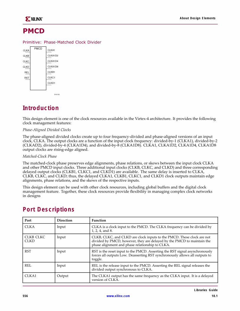
About Design Elements
PMCD
Primitive: Phase-Matched Clock Divider
IntroductionThis design element is one of the clock resources available in the Virtex-4 architecture. It provides the followingclock management features:
Phase-Aligned Divided Clocks
The phase-aligned divided clocks create up to four frequency-divided and phase-aligned versions of an inputclock, CLKA. The output clocks are a function of the input clock frequency: divided-by-1 (CLKA1), divided-by-2(CLKAD2), divided-by-4 (CLKA1D4), and divided-by-8 (CLKA1D8). CLKA1, CLKA1D2, CLKA1D4, CLKA1D8output clocks are rising-edge aligned.
Matched-Clock Phase
The matched-clock phase preserves edge alignments, phase relations, or skews between the input clock CLKAand other PMCD input clocks. Three additional input clocks (CLKB, CLKC, and CLKD) and three correspondingdelayed output clocks (CLKB1, CLKC1, and CLKD1) are available. The same delay is inserted to CLKA,CLKB, CLKC, and CLKD; thus, the delayed CLKA1, CLKB1, CLKC1, and CLKD1 clock outputs maintain edgealignments, phase relations, and the skews of the respective inputs.
This design element can be used with other clock resources, including global buffers and the digital clockmanagement feature. Together, these clock resources provide flexibility in managing complex clock networksin designs
Port DescriptionsPort Direction Function
CLKA Input CLKA is a clock input to the PMCD. The CLKA frequency can be divided by1, 2, 4, and 8.
CLKB CLKCCLKD
Input CLKB, CLKC, and CLKD are clock inputs to the PMCD. These clock are notdivided by PMCD, however, they are delayed by the PMCD to maintain thephase alignment and phase relationship to CLKA.
RST Input RST is the reset input to the PMCD. Asserting the RST signal asynchronouslyforces all outputs Low. Deasserting RST synchronously allows all outputs totoggle.
REL Input REL is the release input to the PMCD. Asserting the REL signal releases thedivided output synchronous to CLKA.
CLKA1 Output The CLKA1 output has the same frequency as the CLKA input. It is a delayedversion of CLKA.
Libraries Guide
556 www.xilinx.com 10.1
About Design Elements
Port Direction Function
CLKA1D2 Output The CLKA1D2 output has the frequency of CLKA divided by two. CLKA1D2 isrising-edge aligned to CLKA1.
CLKA1D4 Output The CLKA1D4 output has the frequency of CLKA divided by four. CLKA1D4 isrising-edge aligned to CLKA1.
CLKA1D8 Output The CLKA1D8 output has the frequency of CLKA divided by eight, CLKA1D8is rising-edge aligned to CLKA1.
CLKB1 CLKC1CLKD1
Output The CLKB1 output is has the same frequency as the CLKB input, a delayedversion of CLKB. The skew between CLKB1 and CLKA1 is the same as the skewbetween CLKB and CLKA inputs. Similarly, CLKC1 is a delayed version ofCLKC, and CLKD1 is a delayed version of CLKD.
Design Entry MethodThis design element can be used in schematics.
Available AttributesAttribute Type Allowed Values Default Description
EN_REL Boolean FALSE, TRUE FALSE This attribute allows for CLKA1D2,CLKA1D4, and CLKA1D8 outputs to bereleased at REL signal assertion. Note:REL is synchronous to CLKA input.
RST_DEASSERT_CLK
String "CLKA," "CLKB","CLKC", or "CLKD”
"CLKA” This attribute allows the deassertion of theRST signal to be synchronous to a selectedPMCD input clock.
For More Information• See the Virtex-4 User Guide.
• See the Virtex-4 Data Sheets.
Libraries Guide
10.1 www.xilinx.com 557
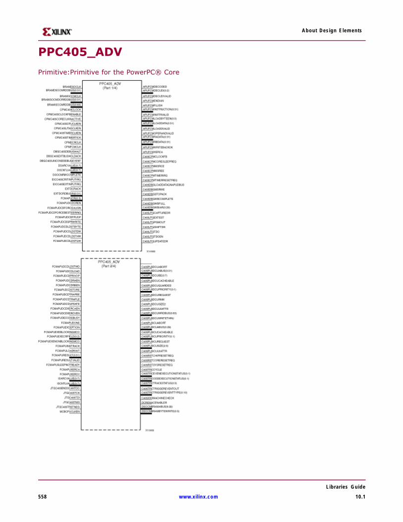
About Design Elements
PPC405_ADV
Primitive:Primitive for the PowerPC® Core
Libraries Guide
558 www.xilinx.com 10.1
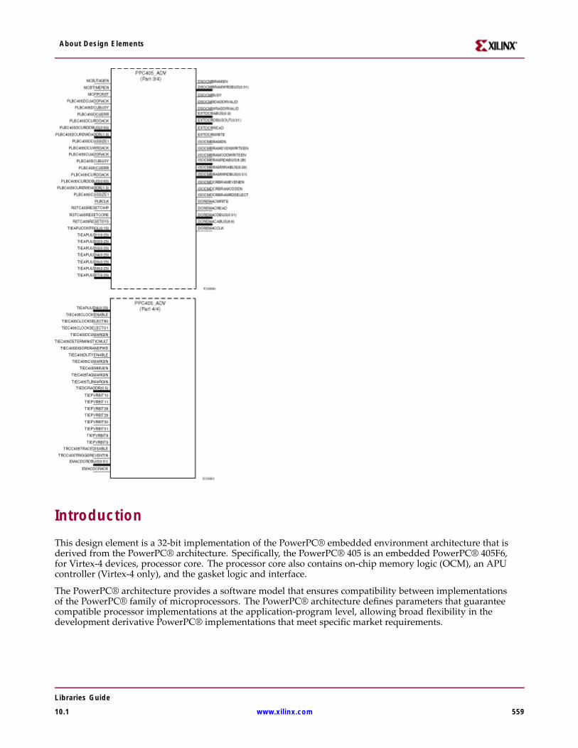
About Design Elements
IntroductionThis design element is a 32-bit implementation of the PowerPC® embedded environment architecture that isderived from the PowerPC® architecture. Specifically, the PowerPC® 405 is an embedded PowerPC® 405F6,for Virtex-4 devices, processor core. The processor core also contains on-chip memory logic (OCM), an APUcontroller (Virtex-4 only), and the gasket logic and interface.
The PowerPC® architecture provides a software model that ensures compatibility between implementationsof the PowerPC® family of microprocessors. The PowerPC® architecture defines parameters that guaranteecompatible processor implementations at the application-program level, allowing broad flexibility in thedevelopment derivative PowerPC® implementations that meet specific market requirements.
Libraries Guide
10.1 www.xilinx.com 559
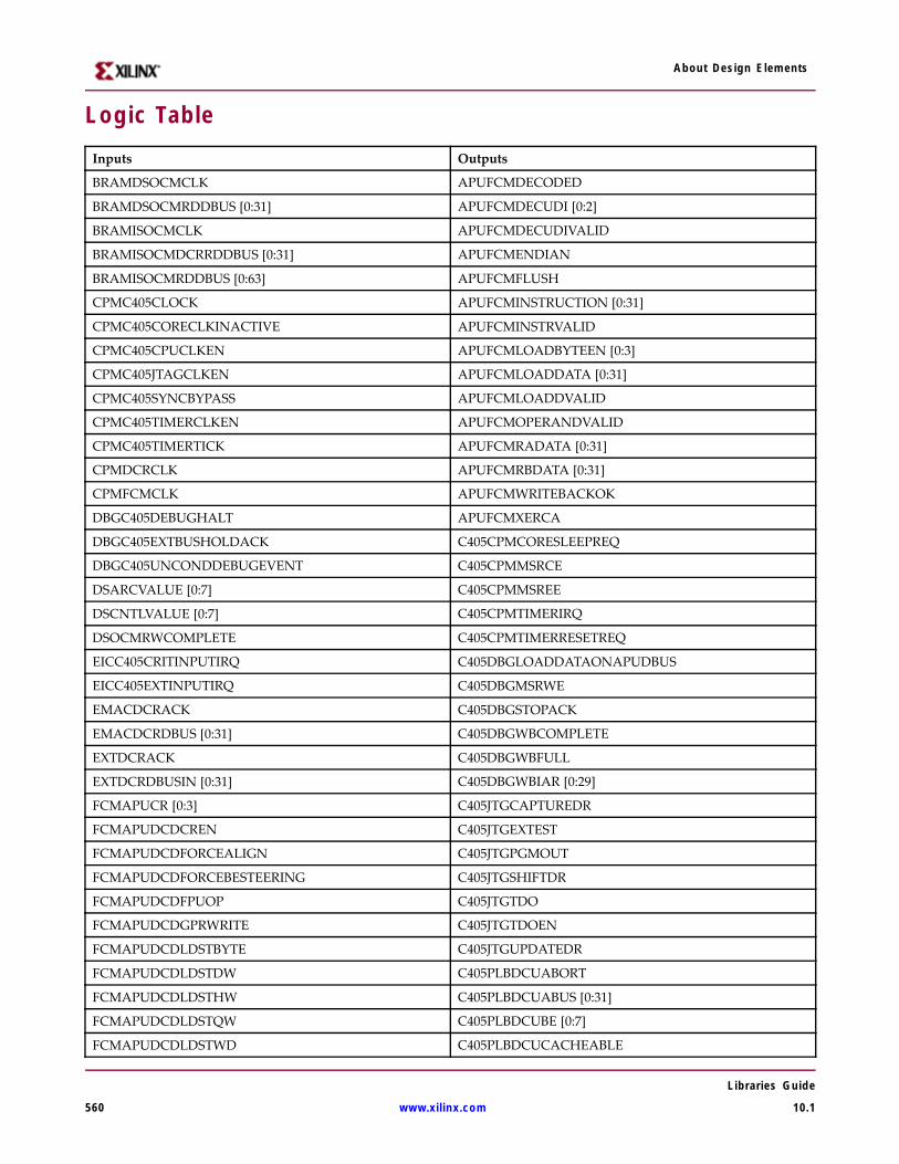
About Design Elements
Logic TableInputs Outputs
BRAMDSOCMCLK APUFCMDECODED
BRAMDSOCMRDDBUS [0:31] APUFCMDECUDI [0:2]
BRAMISOCMCLK APUFCMDECUDIVALID
BRAMISOCMDCRRDDBUS [0:31] APUFCMENDIAN
BRAMISOCMRDDBUS [0:63] APUFCMFLUSH
CPMC405CLOCK APUFCMINSTRUCTION [0:31]
CPMC405CORECLKINACTIVE APUFCMINSTRVALID
CPMC405CPUCLKEN APUFCMLOADBYTEEN [0:3]
CPMC405JTAGCLKEN APUFCMLOADDATA [0:31]
CPMC405SYNCBYPASS APUFCMLOADDVALID
CPMC405TIMERCLKEN APUFCMOPERANDVALID
CPMC405TIMERTICK APUFCMRADATA [0:31]
CPMDCRCLK APUFCMRBDATA [0:31]
CPMFCMCLK APUFCMWRITEBACKOK
DBGC405DEBUGHALT APUFCMXERCA
DBGC405EXTBUSHOLDACK C405CPMCORESLEEPREQ
DBGC405UNCONDDEBUGEVENT C405CPMMSRCE
DSARCVALUE [0:7] C405CPMMSREE
DSCNTLVALUE [0:7] C405CPMTIMERIRQ
DSOCMRWCOMPLETE C405CPMTIMERRESETREQ
EICC405CRITINPUTIRQ C405DBGLOADDATAONAPUDBUS
EICC405EXTINPUTIRQ C405DBGMSRWE
EMACDCRACK C405DBGSTOPACK
EMACDCRDBUS [0:31] C405DBGWBCOMPLETE
EXTDCRACK C405DBGWBFULL
EXTDCRDBUSIN [0:31] C405DBGWBIAR [0:29]
FCMAPUCR [0:3] C405JTGCAPTUREDR
FCMAPUDCDCREN C405JTGEXTEST
FCMAPUDCDFORCEALIGN C405JTGPGMOUT
FCMAPUDCDFORCEBESTEERING C405JTGSHIFTDR
FCMAPUDCDFPUOP C405JTGTDO
FCMAPUDCDGPRWRITE C405JTGTDOEN
FCMAPUDCDLDSTBYTE C405JTGUPDATEDR
FCMAPUDCDLDSTDW C405PLBDCUABORT
FCMAPUDCDLDSTHW C405PLBDCUABUS [0:31]
FCMAPUDCDLDSTQW C405PLBDCUBE [0:7]
FCMAPUDCDLDSTWD C405PLBDCUCACHEABLE
Libraries Guide
560 www.xilinx.com 10.1
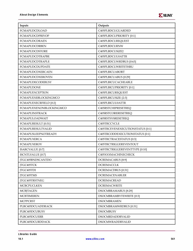
About Design Elements
Inputs Outputs
FCMAPUDCDLOAD C405PLBDCUGUARDED
FCMAPUDCDPRIVOP C405PLBDCUPRIORITY [0:1]
FCMAPUDCDRAEN C405PLBDCUREQUEST
FCMAPUDCDRBEN C405PLBDCURNW
FCMAPUDCDSTORE C405PLBDCUSIZE2
FCMAPUDCDTRAPBE C405PLBDCUU0ATTR
FCMAPUDCDTRAPLE C405PLBDCUWRDBUS [0:63]
FCMAPUDCDUPDATE C405PLBDCUWRITETHRU
FCMAPUDCDXERCAEN C405PLBICUABORT
FCMAPUDCDXEROVEN C405PLBICUABUS [0:29]
FCMAPUDECODEBUSY C405PLBICUCACHEABLE
FCMAPUDONE C405PLBICUPRIORITY [0:1]
FCMAPUEXCEPTION C405PLBICUREQUEST
FCMAPUEXEBLOCKINGMCO C405PLBICUSIZE [2:3]
FCMAPUEXECRFIELD [0:2] C405PLBICUU0ATTR
FCMAPUEXENONBLOCKINGMCO C405RSTCHIPRESETREQ
FCMAPUINSTRACK C405RSTCORERESETREQ
FCMAPULOADWAIT C405RSTSYSRESETREQ
FCMAPURESULT [0:31] C405TRCCYCLE
FCMAPURESULTVALID C405TRCEVENEXECUTIONSTATUS [0:1]
FCMAPUSLEEPNOTREADY C405TRCODDEXECUTIONSTATUS [0:1]
FCMAPUXERCA C405TRCTRACESTATUS [0:3]
FCMAPUXEROV C405TRCTRIGGEREVENTOUT
ISARCVALUE [0:7] C405TRCTRIGGEREVENTTYPE [0:10]
ISCNTLVALUE [0:7] C405XXXMACHINECHECK
JTGC405BNDSCANTDO DCREMACABUS [8:9]
JTGC405TCK DCREMACCLK
JTGC405TDI DCREMACDBUS [0:31]
JTGC405TMS DCREMACENABLER
JTGC405TRSTNEG DCREMACREAD
MCBCPUCLKEN DCREMACWRITE
MCBJTAGEN DSOCMBRAMABUS [8:29]
MCBTIMEREN DSOCMBRAMBYTEWRITE [0:3]
MCPPCRST DSOCMBRAMEN
PLBC405DCUADDRACK DSOCMBRAMWRDBUS [0:31]
PLBC405DCUBUSY DSOCMBUSY
PLBC405DCUERR DSOCMRDADDRVALID
PLBC405DCURDDACK DSOCMWRADDRVALID
Libraries Guide
10.1 www.xilinx.com 561
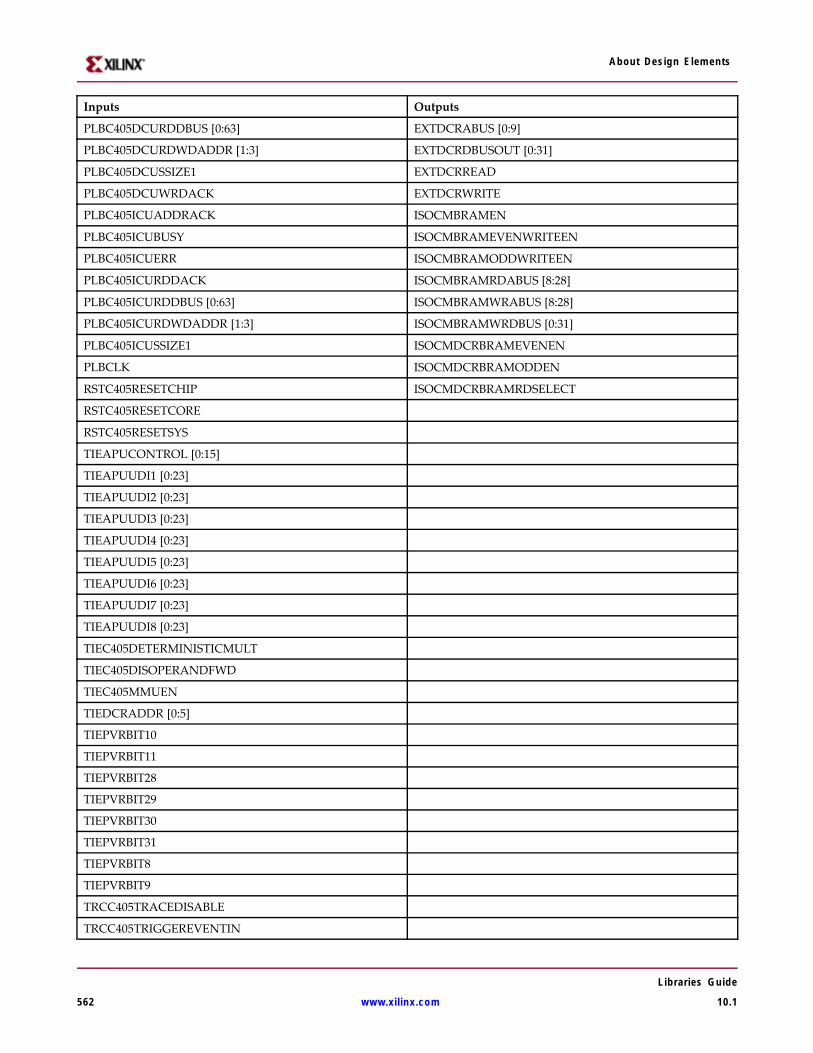
About Design Elements
Inputs Outputs
PLBC405DCURDDBUS [0:63] EXTDCRABUS [0:9]
PLBC405DCURDWDADDR [1:3] EXTDCRDBUSOUT [0:31]
PLBC405DCUSSIZE1 EXTDCRREAD
PLBC405DCUWRDACK EXTDCRWRITE
PLBC405ICUADDRACK ISOCMBRAMEN
PLBC405ICUBUSY ISOCMBRAMEVENWRITEEN
PLBC405ICUERR ISOCMBRAMODDWRITEEN
PLBC405ICURDDACK ISOCMBRAMRDABUS [8:28]
PLBC405ICURDDBUS [0:63] ISOCMBRAMWRABUS [8:28]
PLBC405ICURDWDADDR [1:3] ISOCMBRAMWRDBUS [0:31]
PLBC405ICUSSIZE1 ISOCMDCRBRAMEVENEN
PLBCLK ISOCMDCRBRAMODDEN
RSTC405RESETCHIP ISOCMDCRBRAMRDSELECT
RSTC405RESETCORE
RSTC405RESETSYS
TIEAPUCONTROL [0:15]
TIEAPUUDI1 [0:23]
TIEAPUUDI2 [0:23]
TIEAPUUDI3 [0:23]
TIEAPUUDI4 [0:23]
TIEAPUUDI5 [0:23]
TIEAPUUDI6 [0:23]
TIEAPUUDI7 [0:23]
TIEAPUUDI8 [0:23]
TIEC405DETERMINISTICMULT
TIEC405DISOPERANDFWD
TIEC405MMUEN
TIEDCRADDR [0:5]
TIEPVRBIT10
TIEPVRBIT11
TIEPVRBIT28
TIEPVRBIT29
TIEPVRBIT30
TIEPVRBIT31
TIEPVRBIT8
TIEPVRBIT9
TRCC405TRACEDISABLE
TRCC405TRIGGEREVENTIN
Libraries Guide
562 www.xilinx.com 10.1

About Design Elements
Design Entry MethodThis design element can be used in schematics.
For More Information• See the Virtex-4 User Guide.
• See the Virtex-4 Data Sheets.
Libraries Guide
10.1 www.xilinx.com 563
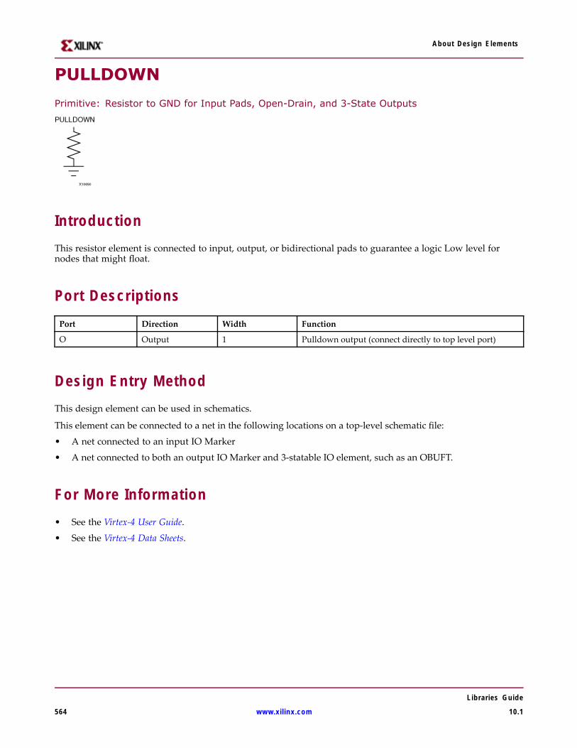
About Design Elements
PULLDOWN
Primitive: Resistor to GND for Input Pads, Open-Drain, and 3-State Outputs
IntroductionThis resistor element is connected to input, output, or bidirectional pads to guarantee a logic Low level fornodes that might float.
Port DescriptionsPort Direction Width Function
O Output 1 Pulldown output (connect directly to top level port)
Design Entry MethodThis design element can be used in schematics.
This element can be connected to a net in the following locations on a top-level schematic file:
• A net connected to an input IO Marker
• A net connected to both an output IO Marker and 3-statable IO element, such as an OBUFT.
For More Information• See the Virtex-4 User Guide.
• See the Virtex-4 Data Sheets.
Libraries Guide
564 www.xilinx.com 10.1
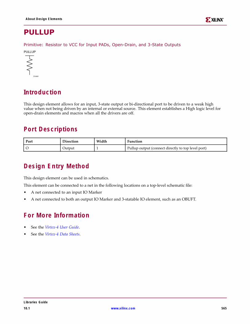
About Design Elements
PULLUP
Primitive: Resistor to VCC for Input PADs, Open-Drain, and 3-State Outputs
IntroductionThis design element allows for an input, 3-state output or bi-directional port to be driven to a weak highvalue when not being driven by an internal or external source. This element establishes a High logic level foropen-drain elements and macros when all the drivers are off.
Port DescriptionsPort Direction Width Function
O Output 1 Pullup output (connect directly to top level port)
Design Entry MethodThis design element can be used in schematics.
This element can be connected to a net in the following locations on a top-level schematic file:
• A net connected to an input IO Marker
• A net connected to both an output IO Marker and 3-statable IO element, such as an OBUFT.
For More Information• See the Virtex-4 User Guide.
• See the Virtex-4 Data Sheets.
Libraries Guide
10.1 www.xilinx.com 565
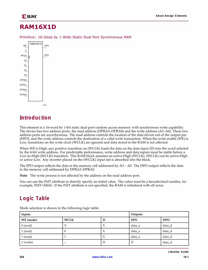
About Design Elements
RAM16X1D
Primitive: 16-Deep by 1-Wide Static Dual Port Synchronous RAM
IntroductionThis element is a 16-word by 1-bit static dual port random access memory with synchronous write capability.The device has two address ports: the read address (DPRA3–DPRA0) and the write address (A3–A0). These twoaddress ports are asynchronous. The read address controls the location of the data driven out of the output pin(DPO), and the write address controls the destination of a valid write transaction. When the write enable (WE) isLow, transitions on the write clock (WCLK) are ignored and data stored in the RAM is not affected.
When WE is High, any positive transition on (WCLK) loads the data on the data input (D) into the word selectedby the 4-bit write address. For predictable performance, write address and data inputs must be stable before aLow-to-High (WCLK) transition. This RAM block assumes an active-High (WCLK). (WCLK) can be active-Highor active-Low. Any inverter placed on the (WCLK) input net is absorbed into the block.
The SPO output reflects the data in the memory cell addressed by A3 – A0. The DPO output reflects the datain the memory cell addressed by DPRA3–DPRA0.
Note The write process is not affected by the address on the read address port.
You can use the INIT attribute to directly specify an initial value. The value must be a hexadecimal number, forexample, INIT=ABAC. If the INIT attribute is not specified, the RAM is initialized with all zeros.
Logic TableMode selection is shown in the following logic table:
Inputs Outputs
WE (mode) WCLK D SPO DPO
0 (read) X X data_a data_d
1 (read) 0 X data_a data_d
1 (read) 1 X data_a data_d
1 (write) ↑ D D data_d
Libraries Guide
566 www.xilinx.com 10.1
About Design Elements
Inputs Outputs
WE (mode) WCLK D SPO DPO
1 (read) ↓ X data_a data_d
data_a = word addressed by bits A3-A0
data_d = word addressed by bits DPRA3-DPRA0
Design Entry MethodThis design element can be used in schematics.
Available AttributesAttribute Type Allowed Values Default Description
INIT Hexadecimal Any 16-Bit Value Allzeros.
Initializes RAMs, registers, and look-uptables.
For More Information• See the Virtex-4 User Guide.
• See the Virtex-4 Data Sheets.
Libraries Guide
10.1 www.xilinx.com 567
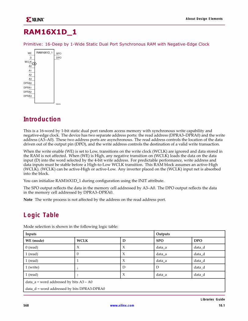
About Design Elements
RAM16X1D_1
Primitive: 16-Deep by 1-Wide Static Dual Port Synchronous RAM with Negative-Edge Clock
IntroductionThis is a 16-word by 1-bit static dual port random access memory with synchronous write capability andnegative-edge clock. The device has two separate address ports: the read address (DPRA3–DPRA0) and the writeaddress (A3–A0). These two address ports are asynchronous. The read address controls the location of the datadriven out of the output pin (DPO), and the write address controls the destination of a valid write transaction.
When the write enable (WE) is set to Low, transitions on the write clock (WCLK) are ignored and data stored inthe RAM is not affected. When (WE) is High, any negative transition on (WCLK) loads the data on the datainput (D) into the word selected by the 4-bit write address. For predictable performance, write address anddata inputs must be stable before a High-to-Low WCLK transition. This RAM block assumes an active-High(WCLK). (WCLK) can be active-High or active-Low. Any inverter placed on the (WCLK) input net is absorbedinto the block.
You can initialize RAM16X1D_1 during configuration using the INIT attribute.
The SPO output reflects the data in the memory cell addressed by A3–A0. The DPO output reflects the datain the memory cell addressed by DPRA3–DPRA0.
Note The write process is not affected by the address on the read address port.
Logic TableMode selection is shown in the following logic table:
Inputs Outputs
WE (mode) WCLK D SPO DPO
0 (read) X X data_a data_d
1 (read) 0 X data_a data_d
1 (read) 1 X data_a data_d
1 (write) ↓ D D data_d
1 (read) ↑ X data_a data_d
data_a = word addressed by bits A3 – A0
data_d = word addressed by bits DPRA3-DPRA0
Libraries Guide
568 www.xilinx.com 10.1
About Design Elements
Port DescriptionsPort Direction Width Function
DPO Output 1 Read-only 1-Bit data output
SPO Output 1 R/W 1-Bit data output
A0 Input 1 R/W address[0] input
A1 Input 1 R/W address[1] input
A2 Input 1 R/W address[2] input
A3 Input 1 R/W address[3] input
D Input 1 Write 1-Bit data input
DPRA0 Input 1 Read-only address[0] input
DPRA1 Input 1 Read-only address[1] input
DPRA2 Input 1 Read-only address[2] input
DPRA3 Input 1 Read-only address[3] input
WCLK Input 1 Write clock input
WE Input 1 Write enable input
Design Entry MethodThis design element can be used in schematics.
Available AttributesAttribute Type Allowed Values Default Description
INIT Hexadecimal Any 16-Bit Value All zeros Initializes RAMs, registers, and look-uptables.
For More Information• See the Virtex-4 User Guide.
• See the Virtex-4 Data Sheets.
Libraries Guide
10.1 www.xilinx.com 569
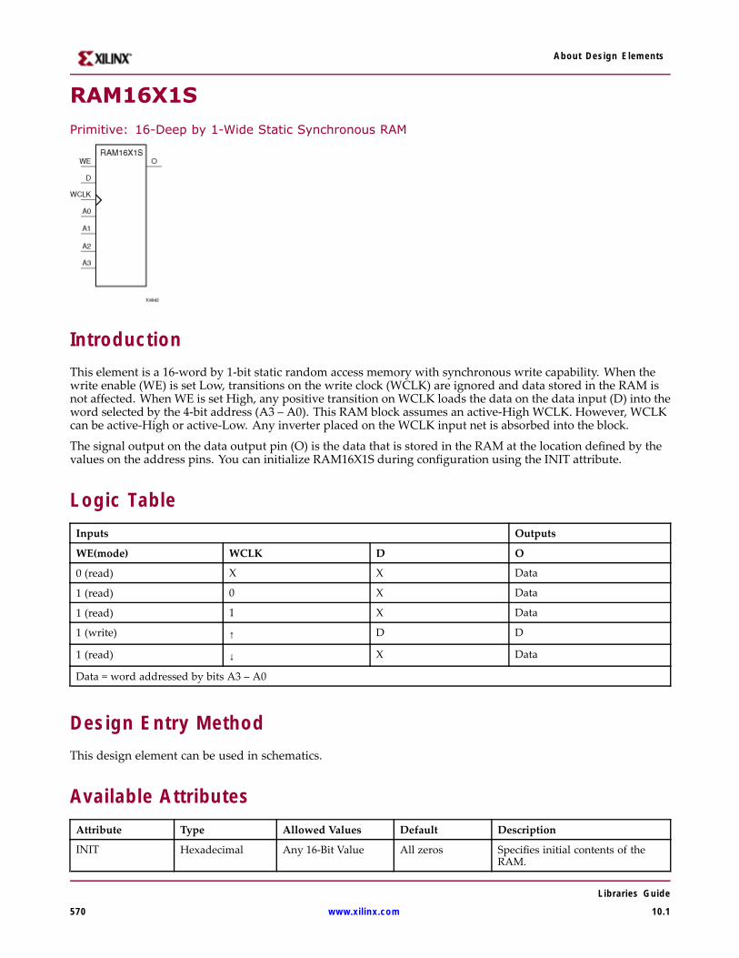
About Design Elements
RAM16X1SPrimitive: 16-Deep by 1-Wide Static Synchronous RAM
IntroductionThis element is a 16-word by 1-bit static random access memory with synchronous write capability. When thewrite enable (WE) is set Low, transitions on the write clock (WCLK) are ignored and data stored in the RAM isnot affected. When WE is set High, any positive transition on WCLK loads the data on the data input (D) into theword selected by the 4-bit address (A3 – A0). This RAM block assumes an active-High WCLK. However, WCLKcan be active-High or active-Low. Any inverter placed on the WCLK input net is absorbed into the block.
The signal output on the data output pin (O) is the data that is stored in the RAM at the location defined by thevalues on the address pins. You can initialize RAM16X1S during configuration using the INIT attribute.
Logic TableInputs Outputs
WE(mode) WCLK D O
0 (read) X X Data
1 (read) 0 X Data
1 (read) 1 X Data
1 (write) ↑ D D
1 (read) ↓ X Data
Data = word addressed by bits A3 – A0
Design Entry MethodThis design element can be used in schematics.
Available AttributesAttribute Type Allowed Values Default Description
INIT Hexadecimal Any 16-Bit Value All zeros Specifies initial contents of theRAM.
Libraries Guide
570 www.xilinx.com 10.1

About Design Elements
For More Information• See the Virtex-4 User Guide.
• See the Virtex-4 Data Sheets.
Libraries Guide
10.1 www.xilinx.com 571

About Design Elements
RAM16X1S_1
Primitive: 16-Deep by 1-Wide Static Synchronous RAM with Negative-Edge Clock
IntroductionThis element is a 16-word by 1-bit static random access memory with synchronous write capability andnegative-edge clock. When the write enable (WE) is Low, transitions on the write clock (WCLK) are ignoredand data stored in the RAM is not affected. When (WE) is High, any negative transition on (WCLK) loads thedata on the data input (D) into the word selected by the 4-bit address (A3 – A0). For predictable performance,address and data inputs must be stable before a High-to-Low WCLK transition. This RAM block assumes anactive-Low (WCLK). However, (WCLK) can be active-High or active-Low. Any inverter placed on the (WCLK)input net is absorbed into the block.
The signal output on the data output pin (O) is the data that is stored in the RAM at the location defined bythe values on the address pins.
You can initialize this element during configuration using the INIT attribute.
Logic TableInputs Outputs
WE(mode) WCLK D O
0 (read) X X Data
1 (read) 0 X Data
1 (read) 1 X Data
1 (write) ↓ D D
1 (read) ↑ X Data
Data = word addressed by bits A3 – A0
Design Entry MethodThis design element can be used in schematics.
Libraries Guide
572 www.xilinx.com 10.1

About Design Elements
Available AttributesAttribute Type Allowed Values Default Description
INIT Hexadecimal Any 16-Bit Value All zeros Specifies initial contents of theRAM.
For More Information• See the Virtex-4 User Guide.
• See the Virtex-4 Data Sheets.
Libraries Guide
10.1 www.xilinx.com 573
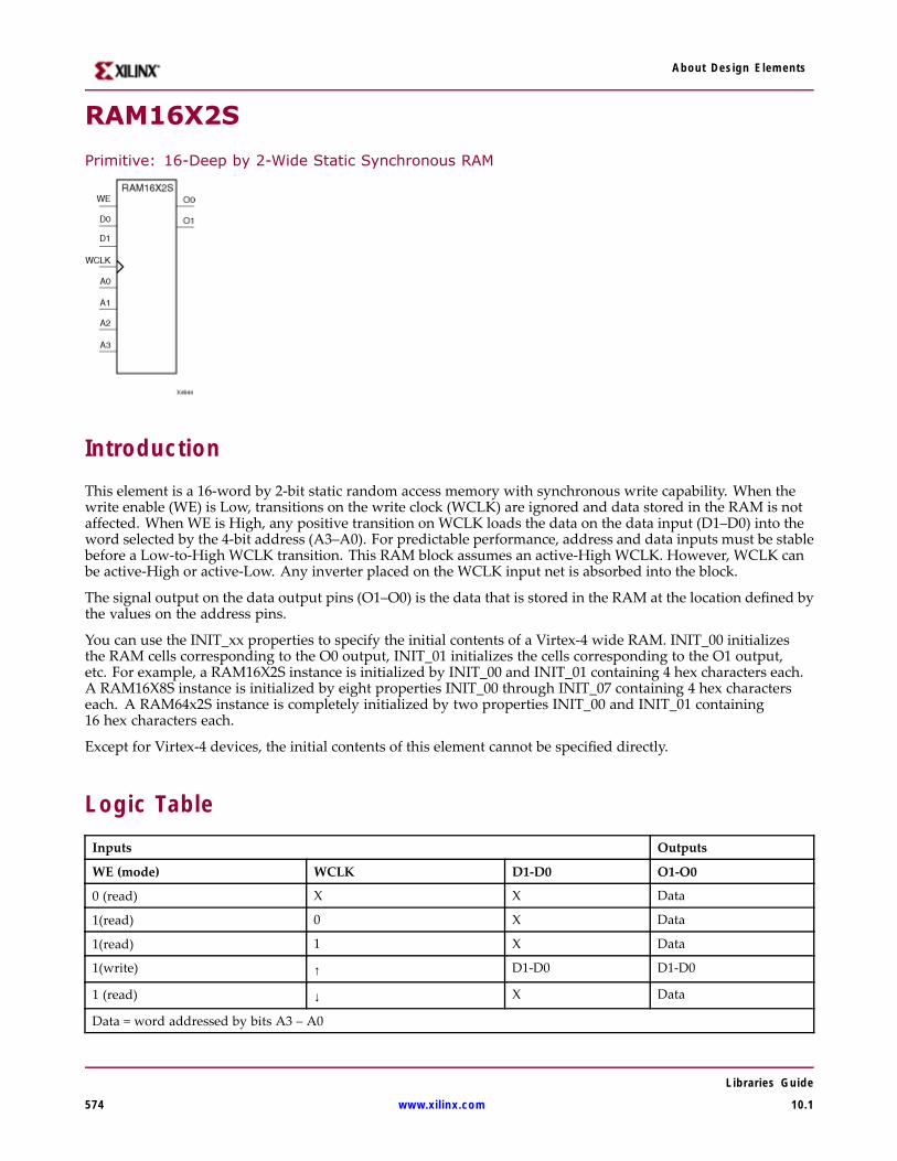
About Design Elements
RAM16X2S
Primitive: 16-Deep by 2-Wide Static Synchronous RAM
IntroductionThis element is a 16-word by 2-bit static random access memory with synchronous write capability. When thewrite enable (WE) is Low, transitions on the write clock (WCLK) are ignored and data stored in the RAM is notaffected. When WE is High, any positive transition on WCLK loads the data on the data input (D1–D0) into theword selected by the 4-bit address (A3–A0). For predictable performance, address and data inputs must be stablebefore a Low-to-High WCLK transition. This RAM block assumes an active-High WCLK. However, WCLK canbe active-High or active-Low. Any inverter placed on the WCLK input net is absorbed into the block.
The signal output on the data output pins (O1–O0) is the data that is stored in the RAM at the location defined bythe values on the address pins.
You can use the INIT_xx properties to specify the initial contents of a Virtex-4 wide RAM. INIT_00 initializesthe RAM cells corresponding to the O0 output, INIT_01 initializes the cells corresponding to the O1 output,etc. For example, a RAM16X2S instance is initialized by INIT_00 and INIT_01 containing 4 hex characters each.A RAM16X8S instance is initialized by eight properties INIT_00 through INIT_07 containing 4 hex characterseach. A RAM64x2S instance is completely initialized by two properties INIT_00 and INIT_01 containing16 hex characters each.
Except for Virtex-4 devices, the initial contents of this element cannot be specified directly.
Logic TableInputs Outputs
WE (mode) WCLK D1-D0 O1-O0
0 (read) X X Data
1(read) 0 X Data
1(read) 1 X Data
1(write) ↑ D1-D0 D1-D0
1 (read) ↓ X Data
Data = word addressed by bits A3 – A0
Libraries Guide
574 www.xilinx.com 10.1

About Design Elements
Design Entry MethodThis design element can be used in schematics.
Available AttributesAttribute Type Allowed Values Default Description
INIT_00 to INIT_01 Hexadecimal Any 16-Bit Value All zeros Initializes RAMs, registers, andlook-up tables.
For More Information• See the Virtex-4 User Guide.
• See the Virtex-4 Data Sheets.
Libraries Guide
10.1 www.xilinx.com 575
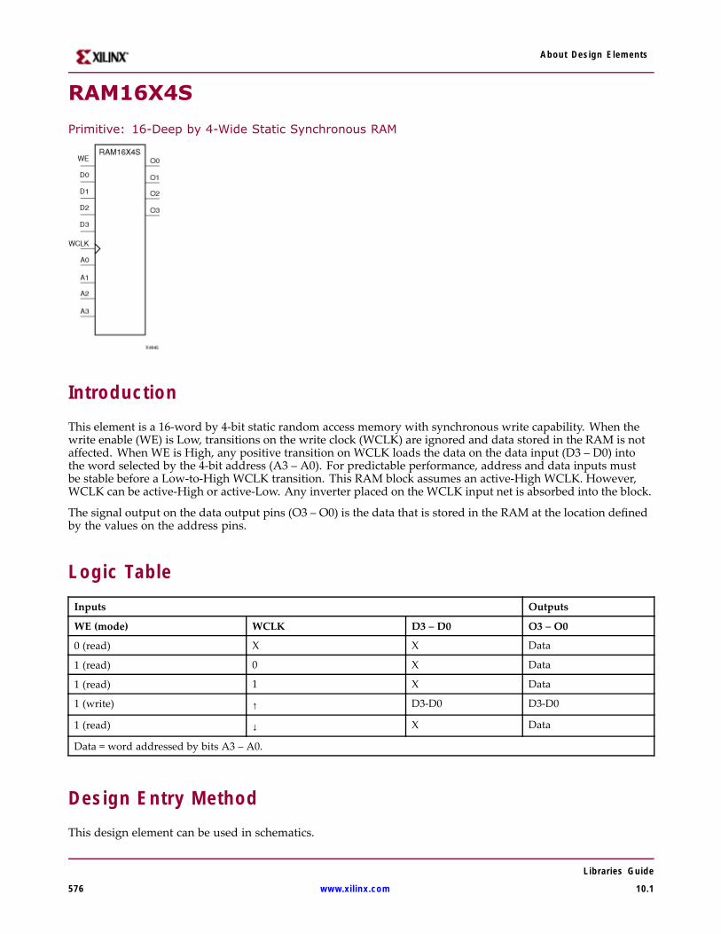
About Design Elements
RAM16X4S
Primitive: 16-Deep by 4-Wide Static Synchronous RAM
IntroductionThis element is a 16-word by 4-bit static random access memory with synchronous write capability. When thewrite enable (WE) is Low, transitions on the write clock (WCLK) are ignored and data stored in the RAM is notaffected. When WE is High, any positive transition on WCLK loads the data on the data input (D3 – D0) intothe word selected by the 4-bit address (A3 – A0). For predictable performance, address and data inputs mustbe stable before a Low-to-High WCLK transition. This RAM block assumes an active-High WCLK. However,WCLK can be active-High or active-Low. Any inverter placed on the WCLK input net is absorbed into the block.
The signal output on the data output pins (O3 – O0) is the data that is stored in the RAM at the location definedby the values on the address pins.
Logic TableInputs Outputs
WE (mode) WCLK D3 – D0 O3 – O0
0 (read) X X Data
1 (read) 0 X Data
1 (read) 1 X Data
1 (write) ↑ D3-D0 D3-D0
1 (read) ↓ X Data
Data = word addressed by bits A3 – A0.
Design Entry MethodThis design element can be used in schematics.
Libraries Guide
576 www.xilinx.com 10.1

About Design Elements
Available AttributesAttribute Type Allowed Values Default Description
INIT_00 to INIT_03 Hexadecimal Any 16-Bit Value All zeros INIT for bit 0 of RAM
For More Information• See the Virtex-4 User Guide.
• See the Virtex-4 Data Sheets.
Libraries Guide
10.1 www.xilinx.com 577

About Design Elements
RAM16X8SPrimitive: 16-Deep by 8-Wide Static Synchronous RAM
IntroductionThis element is a 16-word by 8-bit static random access memory with synchronous write capability. When thewrite enable (WE) is Low, transitions on the write clock (WCLK) are ignored and data stored in the RAM is notaffected. When WE is High, any positive transition on WCLK loads the data on data inputs (D7–D0) into theword selected by the 4-bit address (A3–A0). For predictable performance, address and data inputs must be stablebefore a Low-to-High WCLK transition. This RAM block assumes an active-High WCLK. However, WCLK canbe active-High or active-Low. Any inverter placed on the WCLK input net is absorbed into the block.
The signal output on the data output pins (O7–O0) is the data that is stored in the RAM at the location defined bythe values on the address pins.
Logic TableInputs Outputs
WE (mode) WCLK D7-D0 O7-O0
0 (read) X X Data
1 (read) 0 X Data
1 (read) 1 X Data
1 (write) ↑ D7-D0 D7-D0
1 (read) ↓ X Data
Data = word addressed by bits A3–A0
Design Entry MethodThis design element can be used in schematics.
Available AttributesAttribute Type Allowed Values Default Description
INIT_00 To INIT_07 Hexadecimal Any 16-Bit Value All zeros Initializes RAMs, registers, and look-uptables.
Libraries Guide
578 www.xilinx.com 10.1

About Design Elements
For More Information• See the Virtex-4 User Guide.
• See the Virtex-4 Data Sheets.
Libraries Guide
10.1 www.xilinx.com 579

About Design Elements
RAM32X1SPrimitive: 32-Deep by 1-Wide Static Synchronous RAM
IntroductionThe design element is a 32-word by 1-bit static random access memory with synchronous write capability. Whenthe write enable is Low, transitions on the write clock (WCLK) are ignored and data stored in the RAM is notaffected. When (WE) is High, any positive transition on (WCLK) loads the data on the data input (D) into theword selected by the 5-bit address (A4-A0). For predictable performance, address and data inputs must be stablebefore a Low-to-High (WCLK) transition. This RAM block assumes an active-High (WCLK). However, (WCLK)can be active-High or active-Low. Any inverter placed on the (WCLK) input net is absorbed into the block.
The signal output on the data output pin (O) is the data that is stored in the RAM at the location defined by thevalues on the address pins. You can initialize RAM32X1S during configuration using the INIT attribute.
Logic TableInputs Outputs
WE (Mode) WCLK D O
0 (read) X X Data
1 (read) 0 X Data
1 (read) 1 X Data
1 (write) ↓ D D
1 (read) ↑ X Data
Design Entry MethodThis design element can be used in schematics.
Available Attributes
Attribute Type Allowed Values Default Descriptions
INIT Hexadecimal Any 32-Bit Value All zeros Specifies initial contents of the RAM.
Libraries Guide
580 www.xilinx.com 10.1

About Design Elements
For More Information• See the Virtex-4 User Guide.
• See the Virtex-4 Data Sheets.
Libraries Guide
10.1 www.xilinx.com 581
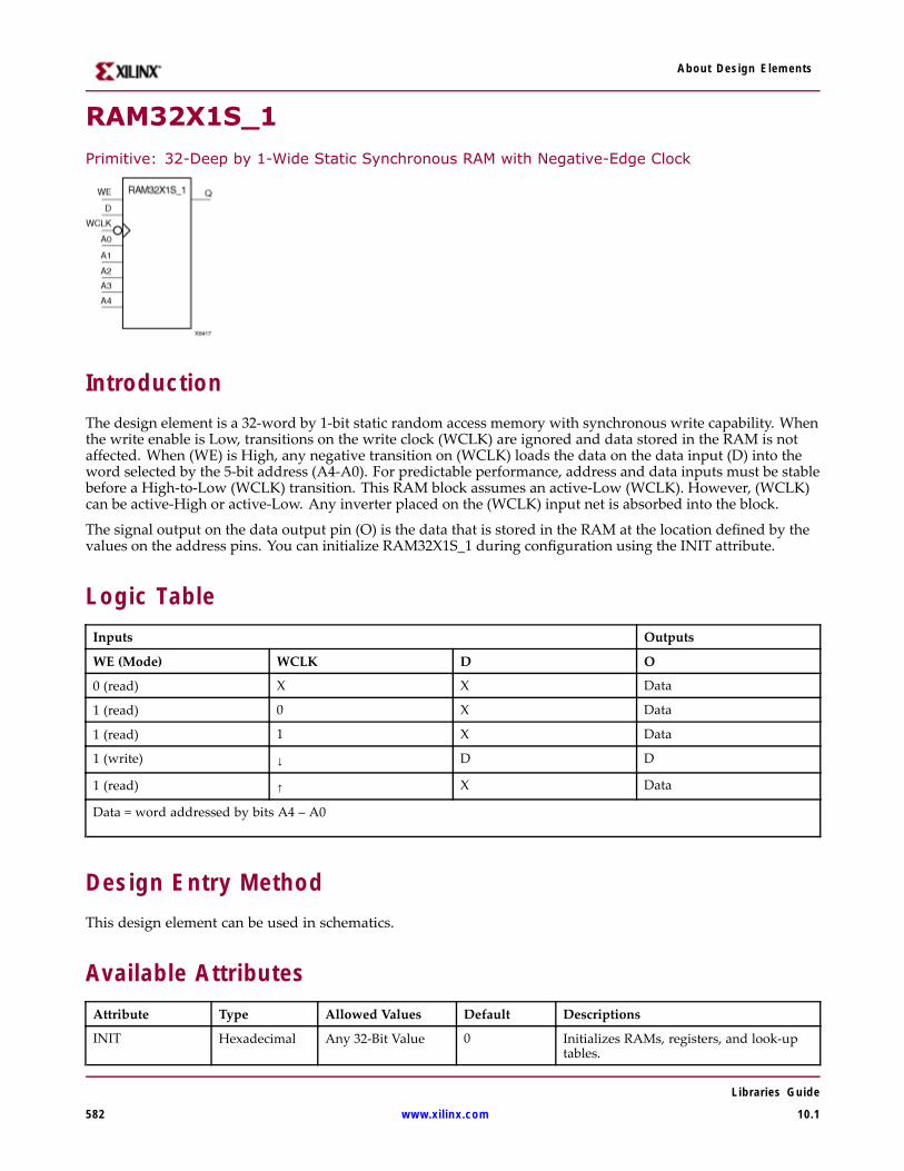
About Design Elements
RAM32X1S_1Primitive: 32-Deep by 1-Wide Static Synchronous RAM with Negative-Edge Clock
IntroductionThe design element is a 32-word by 1-bit static random access memory with synchronous write capability. Whenthe write enable is Low, transitions on the write clock (WCLK) are ignored and data stored in the RAM is notaffected. When (WE) is High, any negative transition on (WCLK) loads the data on the data input (D) into theword selected by the 5-bit address (A4-A0). For predictable performance, address and data inputs must be stablebefore a High-to-Low (WCLK) transition. This RAM block assumes an active-Low (WCLK). However, (WCLK)can be active-High or active-Low. Any inverter placed on the (WCLK) input net is absorbed into the block.
The signal output on the data output pin (O) is the data that is stored in the RAM at the location defined by thevalues on the address pins. You can initialize RAM32X1S_1 during configuration using the INIT attribute.
Logic TableInputs Outputs
WE (Mode) WCLK D O
0 (read) X X Data
1 (read) 0 X Data
1 (read) 1 X Data
1 (write) ↓ D D
1 (read) ↑ X Data
Data = word addressed by bits A4 – A0
Design Entry MethodThis design element can be used in schematics.
Available AttributesAttribute Type Allowed Values Default Descriptions
INIT Hexadecimal Any 32-Bit Value 0 Initializes RAMs, registers, and look-uptables.
Libraries Guide
582 www.xilinx.com 10.1

About Design Elements
For More Information• See the Virtex-4 User Guide.
• See the Virtex-4 Data Sheets.
Libraries Guide
10.1 www.xilinx.com 583

About Design Elements
RAM32X2S
Primitive: 32-Deep by 2-Wide Static Synchronous RAM
IntroductionThe design element is a 32-word by 2-bit static random access memory with synchronous write capability. Whenthe write enable (WE) is Low, transitions on the write clock (WCLK) are ignored and data stored in the RAM isnot affected. When (WE) is High, any positive transition on (WCLK) loads the data on the data input (D1-D0)into the word selected by the 5-bit address (A4-A0). For predictable performance, address and data inputs mustbe stable before a Low-to-High (WCLK) transition. This RAM block assumes an active-High (WCLK). However,(WCLK) can be active-High or active-Low. Any inverter placed on the (WCLK) input net is absorbed into theblock. The signal output on the data output pins (O1-O0) is the data that is stored in the RAM at the locationdefined by the values on the address pins.
You can use the INIT_00 and INIT_01 properties to specify the initial contents of RAM32X2S.
Logic TableInputs Outputs
WE (Mode) WCLK D O0-O1
0 (read) X X Data
1 (read) 0 X Data
1 (read) 1 X Data
1 (write) ↑ D1-D0 D1-D0
1 (read) ↓ X Data
Data = word addressed by bits A4 A0
Design Entry MethodThis design element can be used in schematics.
Libraries Guide
584 www.xilinx.com 10.1
About Design Elements
Available AttributesAttribute Type Allowed Values Default Descriptions
INIT_00 Hexadecimal Any 32-Bit Value All zeros INIT for bit 0 of RAM.
INIT_01 Hexadecimal Any 32-Bit Value All zeros INIT for bit 1 of RAM.
For More Information• See the Virtex-4 User Guide.
• See the Virtex-4 Data Sheets.
Libraries Guide
10.1 www.xilinx.com 585
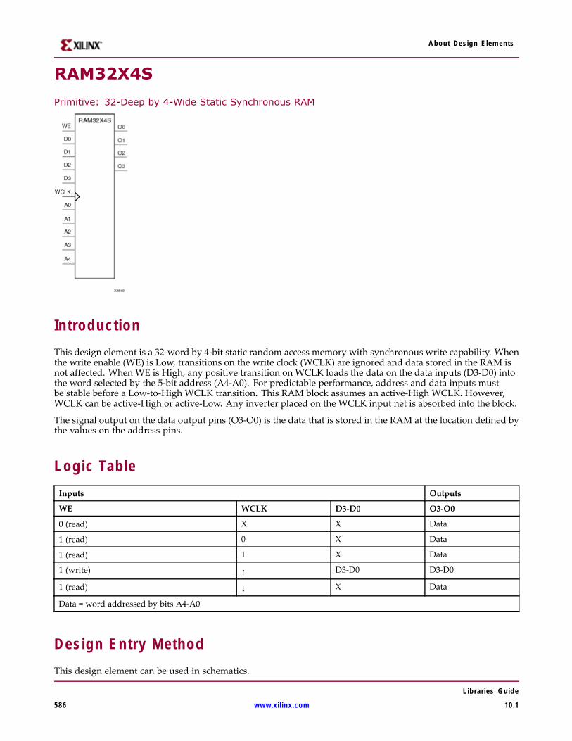
About Design Elements
RAM32X4S
Primitive: 32-Deep by 4-Wide Static Synchronous RAM
IntroductionThis design element is a 32-word by 4-bit static random access memory with synchronous write capability. Whenthe write enable (WE) is Low, transitions on the write clock (WCLK) are ignored and data stored in the RAM isnot affected. When WE is High, any positive transition on WCLK loads the data on the data inputs (D3-D0) intothe word selected by the 5-bit address (A4-A0). For predictable performance, address and data inputs mustbe stable before a Low-to-High WCLK transition. This RAM block assumes an active-High WCLK. However,WCLK can be active-High or active-Low. Any inverter placed on the WCLK input net is absorbed into the block.
The signal output on the data output pins (O3-O0) is the data that is stored in the RAM at the location defined bythe values on the address pins.
Logic TableInputs Outputs
WE WCLK D3-D0 O3-O0
0 (read) X X Data
1 (read) 0 X Data
1 (read) 1 X Data
1 (write) ↑ D3-D0 D3-D0
1 (read) ↓ X Data
Data = word addressed by bits A4-A0
Design Entry MethodThis design element can be used in schematics.
Libraries Guide
586 www.xilinx.com 10.1
About Design Elements
Available AttributesAttribute Type Allowed Values Default Description
INIT_00 Hexadecimal Any 32-Bit Value All zeros INIT for bit 0 of RAM.
INIT_01 Hexadecimal Any 32-Bit Value All zeros INIT for bit 1 of RAM.
INIT_02 Hexadecimal Any 32-Bit Value All zeros INIT for bit 2 of RAM.
INIT_03 Hexadecimal Any 32-Bit Value All zeros INIT for bit 3 of RAM.
For More Information• See the Virtex-4 User Guide.
• See the Virtex-4 Data Sheets.
Libraries Guide
10.1 www.xilinx.com 587
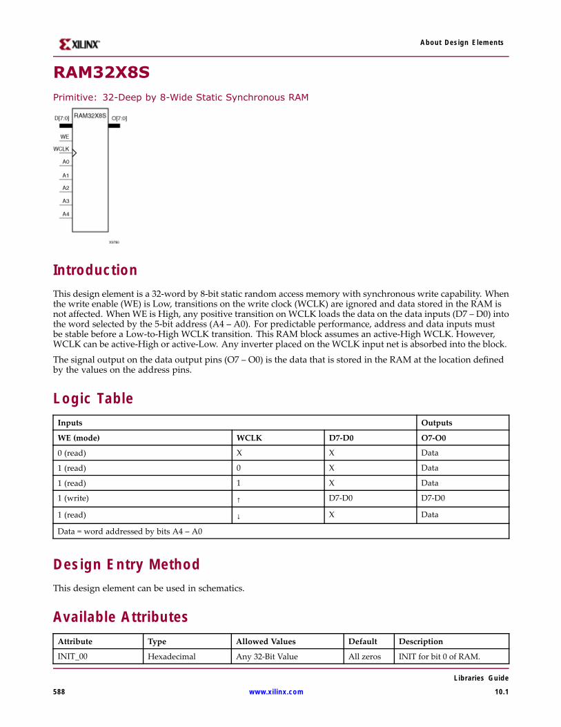
About Design Elements
RAM32X8SPrimitive: 32-Deep by 8-Wide Static Synchronous RAM
IntroductionThis design element is a 32-word by 8-bit static random access memory with synchronous write capability. Whenthe write enable (WE) is Low, transitions on the write clock (WCLK) are ignored and data stored in the RAM isnot affected. When WE is High, any positive transition on WCLK loads the data on the data inputs (D7 – D0) intothe word selected by the 5-bit address (A4 – A0). For predictable performance, address and data inputs mustbe stable before a Low-to-High WCLK transition. This RAM block assumes an active-High WCLK. However,WCLK can be active-High or active-Low. Any inverter placed on the WCLK input net is absorbed into the block.
The signal output on the data output pins (O7 – O0) is the data that is stored in the RAM at the location definedby the values on the address pins.
Logic TableInputs Outputs
WE (mode) WCLK D7-D0 O7-O0
0 (read) X X Data
1 (read) 0 X Data
1 (read) 1 X Data
1 (write) ↑ D7-D0 D7-D0
1 (read) ↓ X Data
Data = word addressed by bits A4 – A0
Design Entry MethodThis design element can be used in schematics.
Available AttributesAttribute Type Allowed Values Default Description
INIT_00 Hexadecimal Any 32-Bit Value All zeros INIT for bit 0 of RAM.
Libraries Guide
588 www.xilinx.com 10.1
About Design Elements
Attribute Type Allowed Values Default Description
INIT_01 Hexadecimal Any 32-Bit Value All zeros INIT for bit 1 of RAM.
INIT_02 Hexadecimal Any 32-Bit Value All zeros INIT for bit 2 of RAM.
INIT_03 Hexadecimal Any 32-Bit Value All zeros INIT for bit 3 of RAM.
INIT_04 Hexadecimal Any 32-Bit Value All zeros INIT for bit 4 of RAM.
INIT_05 Hexadecimal Any 32-Bit Value All zeros INIT for bit 5 of RAM.
INIT_06 Hexadecimal Any 32-Bit Value All zeros INIT for bit 6 of RAM.
INIT_07 Hexadecimal Any 32-Bit Value All zeros INIT for bit 7 of RAM.
For More Information• See the Virtex-4 User Guide.
• See the Virtex-4 Data Sheets.
Libraries Guide
10.1 www.xilinx.com 589

About Design Elements
RAM64X1SPrimitive: 64-Deep by 1-Wide Static Synchronous RAM
IntroductionThis design element is a 64-word by 1-bit static random access memory (RAM) with synchronous write capability.When the write enable is set Low, transitions on the write clock (WCLK) are ignored and data stored in the RAMis not affected. When WE is set High, any positive transition on WCLK loads the data on the data input (D) intothe word selected by the 6-bit address (A5 - A0). This RAM block assumes an active-High WCLK. However,WCLK can be active-High or active-Low. Any inverter placed on the WCLK input net is absorbed into the block.
The signal output on the data output pin (O) is the data that is stored in the RAM at the location defined bythe values on the address pins.
You can initialize this element during configuration using the INIT attribute.
Logic TableMode selection is shown in the following logic table
Inputs Outputs
WE (mode) WCLK D O
0 (read) X X Data
1 (read) 0 X Data
1 (read) 1 X Data
1 (write) ↑ D D
1 (read) ↓ X Data
Data = word addressed by bits A5 – A0
Design Entry MethodThis design element can be used in schematics.
Available AttributesAttribute Type Allowed Values Default Description
INIT Hexadecimal Any 64-Bit Value All zeros Initializes ROMs, RAMs, registers, and look-uptables.
Libraries Guide
590 www.xilinx.com 10.1

About Design Elements
For More Information• See the Virtex-4 User Guide.
• See the Virtex-4 Data Sheets.
Libraries Guide
10.1 www.xilinx.com 591
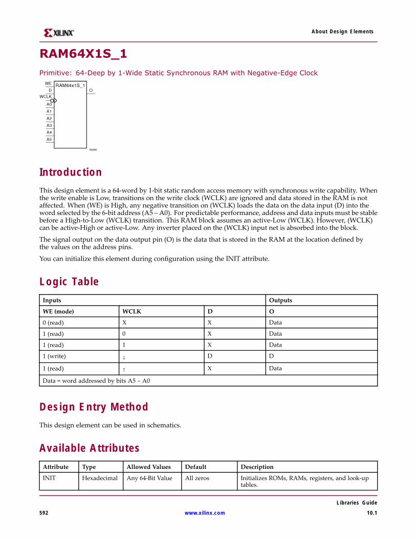
About Design Elements
RAM64X1S_1Primitive: 64-Deep by 1-Wide Static Synchronous RAM with Negative-Edge Clock
IntroductionThis design element is a 64-word by 1-bit static random access memory with synchronous write capability. Whenthe write enable is Low, transitions on the write clock (WCLK) are ignored and data stored in the RAM is notaffected. When (WE) is High, any negative transition on (WCLK) loads the data on the data input (D) into theword selected by the 6-bit address (A5 – A0). For predictable performance, address and data inputs must be stablebefore a High-to-Low (WCLK) transition. This RAM block assumes an active-Low (WCLK). However, (WCLK)can be active-High or active-Low. Any inverter placed on the (WCLK) input net is absorbed into the block.
The signal output on the data output pin (O) is the data that is stored in the RAM at the location defined bythe values on the address pins.
You can initialize this element during configuration using the INIT attribute.
Logic TableInputs Outputs
WE (mode) WCLK D O
0 (read) X X Data
1 (read) 0 X Data
1 (read) 1 X Data
1 (write) ↓ D D
1 (read) ↑ X Data
Data = word addressed by bits A5 – A0
Design Entry MethodThis design element can be used in schematics.
Available AttributesAttribute Type Allowed Values Default Description
INIT Hexadecimal Any 64-Bit Value All zeros Initializes ROMs, RAMs, registers, and look-uptables.
Libraries Guide
592 www.xilinx.com 10.1

About Design Elements
For More Information• See the Virtex-4 User Guide.
• See the Virtex-4 Data Sheets.
Libraries Guide
10.1 www.xilinx.com 593
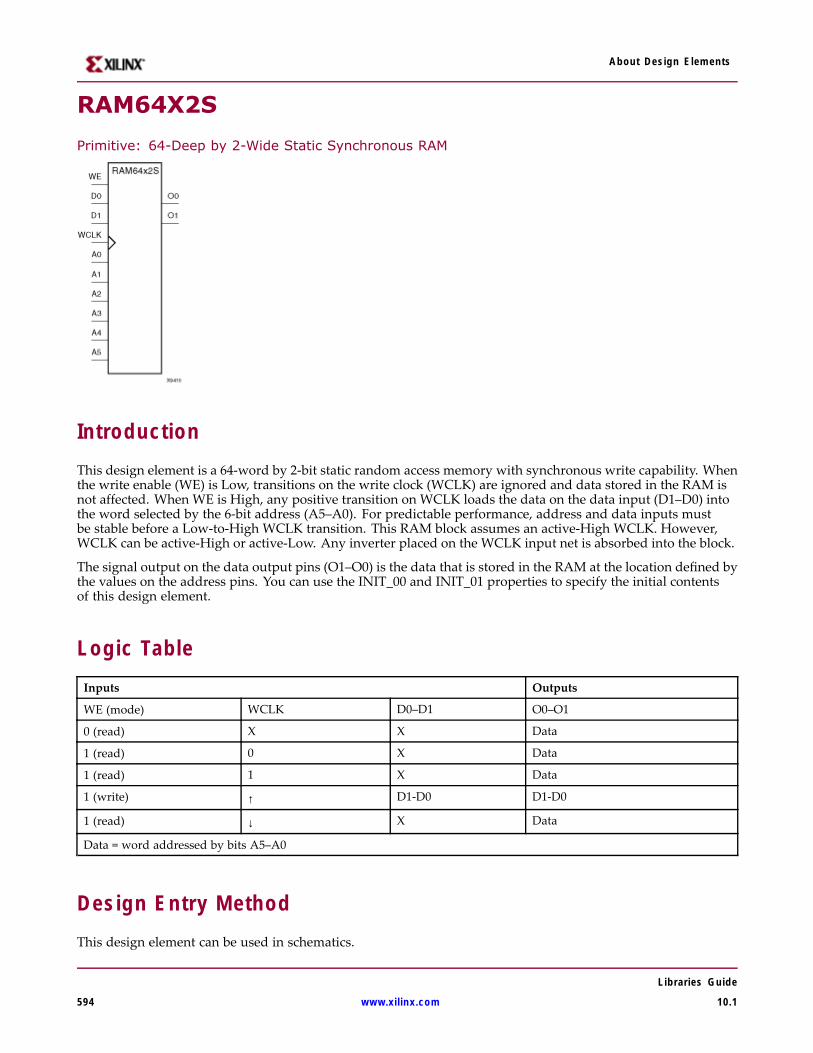
About Design Elements
RAM64X2S
Primitive: 64-Deep by 2-Wide Static Synchronous RAM
IntroductionThis design element is a 64-word by 2-bit static random access memory with synchronous write capability. Whenthe write enable (WE) is Low, transitions on the write clock (WCLK) are ignored and data stored in the RAM isnot affected. When WE is High, any positive transition on WCLK loads the data on the data input (D1–D0) intothe word selected by the 6-bit address (A5–A0). For predictable performance, address and data inputs mustbe stable before a Low-to-High WCLK transition. This RAM block assumes an active-High WCLK. However,WCLK can be active-High or active-Low. Any inverter placed on the WCLK input net is absorbed into the block.
The signal output on the data output pins (O1–O0) is the data that is stored in the RAM at the location defined bythe values on the address pins. You can use the INIT_00 and INIT_01 properties to specify the initial contentsof this design element.
Logic TableInputs Outputs
WE (mode) WCLK D0–D1 O0–O1
0 (read) X X Data
1 (read) 0 X Data
1 (read) 1 X Data
1 (write) ↑ D1-D0 D1-D0
1 (read) ↓ X Data
Data = word addressed by bits A5–A0
Design Entry MethodThis design element can be used in schematics.
Libraries Guide
594 www.xilinx.com 10.1
About Design Elements
Available AttributesAttribute Type Allowed Values Default Description
INIT_00 Hexadecimal Any 64-Bit Value All zeros Initializes RAMs, registers, and look-up tables.
INIT_01 Hexadecimal Any 64-Bit Value All zeros Initializes RAMs, registers, and look-up tables.
For More Information• See the Virtex-4 User Guide.
• See the Virtex-4 Data Sheets.
Libraries Guide
10.1 www.xilinx.com 595
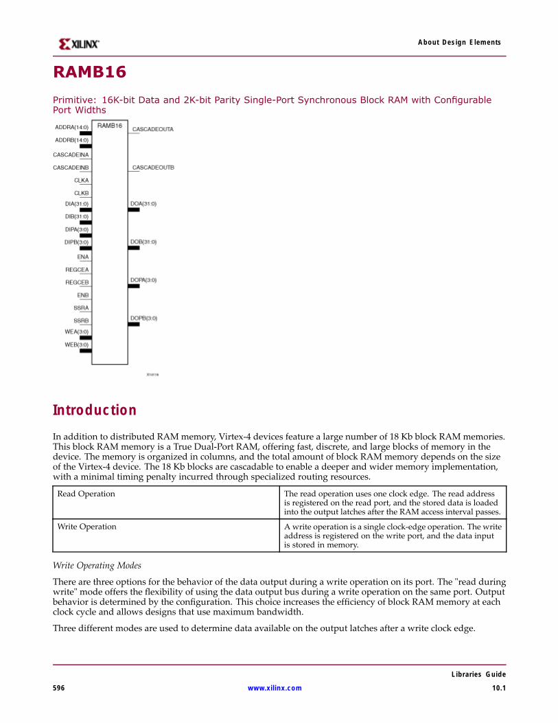
About Design Elements
RAMB16
Primitive: 16K-bit Data and 2K-bit Parity Single-Port Synchronous Block RAM with ConfigurablePort Widths
IntroductionIn addition to distributed RAMmemory, Virtex-4 devices feature a large number of 18 Kb block RAMmemories.This block RAM memory is a True Dual-Port RAM, offering fast, discrete, and large blocks of memory in thedevice. The memory is organized in columns, and the total amount of block RAM memory depends on the sizeof the Virtex-4 device. The 18 Kb blocks are cascadable to enable a deeper and wider memory implementation,with a minimal timing penalty incurred through specialized routing resources.
Read Operation The read operation uses one clock edge. The read addressis registered on the read port, and the stored data is loadedinto the output latches after the RAM access interval passes.
Write Operation A write operation is a single clock-edge operation. The writeaddress is registered on the write port, and the data inputis stored in memory.
Write Operating Modes
There are three options for the behavior of the data output during a write operation on its port. The "read duringwrite" mode offers the flexibility of using the data output bus during a write operation on the same port. Outputbehavior is determined by the configuration. This choice increases the efficiency of block RAM memory at eachclock cycle and allows designs that use maximum bandwidth.
Three different modes are used to determine data available on the output latches after a write clock edge.
Libraries Guide
596 www.xilinx.com 10.1

About Design Elements
WRITE_FIRST or Transparent Mode (Default) The input data is simultaneously written into memory andstored in the data output (transparent write)
READ_FIRST or Read-Before-Write Mode Data previously stored at the write address appears onthe output latches, while the input data is being stored inmemory (read before write).
NO_CHANGE Mode The output latches remain unchanged during a writeoperation.
Mode selection is set by configuration. One of these three modes is set individually for each port by an attribute.The default mode is WRITE_FIRST.
Port DescriptionsOutput Latches Synchronous Set/Reset - SRVAL (SRVAL_A & SRVAL_B)
The SRVAL_A and SRVAL_B (dual-port) attributes define output latch values when the SSR input is asserted.The width of the SRVAL (SRVAL_A and SRVAL_B) attribute is the port width, as shown in the following table:
Port Width Values andData Width DOP Bus DO Bus SRVAL
1 NA <0> 1
2 NA <1:0> 2
4 NA <3:0> 4
9 <0> <7:0> (1+8) = 9
18 <1:0> <15:0> (2+16) = 18
36 <3:0> <31:0> (4 + 32) = 36
Optional Output Register On/Off Switch - DO[A/B]_REG
This attribute sets the number of pipeline register at A/B output of RAMB16. The valid values are 0 (default) or 1.
Clock Inversion at Output Register Switch - INVERT_CLK_DO[A/B]_REG
When set to TRUE, the clock input to the pipeline register at A/B output of RAMB16 is inverted. The defaultvalue is FALSE.
Extended Mode Address Determinant - RAM_EXTENSION_[A/B]
This attribute determines whether the block RAM of interest has its A/B port as UPPER/LOWER address whenusing the cascade mode. In the cascading mode, READ_WIDTH_[A/B] and WRITE_WIDTH_[A/B] should be setto 1. When the block RAM is not used in cascade mode, the default value is NONE.
Read Width - READ_WIDTH_[A/B]
This attribute determines the A/B read port width of the block RAM. The valid values are: 0 (default), 1, 2, 4, 9,18, and 36. The READ_WIDTH_[A/B] for both the ports should not be set to zero at the same time.
Write Width - WRITE_WIDTH_[A/B]
This attribute determines the A/B write port width of the block RAM. The valid values are: 0 (default), 1, 2, 4, 9,18, and 36.
Write Mode - WRITE_MODE_[A/B]
This attribute determines the write mode of the A/B input ports. The possible values are WRITE_FIRST (default),READ_FIRST, and NO_CHANGE.
RAMB16 Location Constraints
Libraries Guide
10.1 www.xilinx.com 597
About Design Elements
Block RAM instances can have LOC properties attached to them to constrain placement. Block RAM placementlocations differ from the convention used for naming CLB locations, allowing LOC properties to transfer easilyfrom array to array. The LOC properties use the following form: LOC = RAMB16_X#Y#
The RAMB16_X0Y0 is the bottom-left block RAM location on the device.
Design Entry MethodThis design element can be used in schematics.
Available AttributesAttribute Type Allowed Values Default Description
DOA_REG Integer 0 or 1 0 Optional output registers on A port
DOB_REG Integer 0 or 1 0 Optional output registers on B port.
INIT_00 to INIT_39 Hexadecimal Any 256-Bit Value All zeros To change the initial contents ofthe RAM to anything other than allzero’s.
INIT_0A to INIT_0F Hexadecimal Any 256-Bit Value All zeros To change the initial contents ofthe RAM to anything other than allzero’s.
INIT_1A to INIT_1F Hexadecimal Any 256-Bit Value All zeros To change the initial contents ofthe RAM to anything other than allzero’s.
INIT_2A to INIT_2F Hexadecimal Any 256-Bit Value All zeros To change the initial contents ofthe RAM to anything other than allzero’s.
INIT_3A to INIT_3F Hexadecimal Any 256-Bit Value All zeros To change the initial contents ofthe RAM to anything other than allzero’s.
INIT_A Hexadecimal Any 36-Bit Value All zeros Initial values on A output port.
INIT_B Hexadecimal Any 36-Bit Value All zeros Initial values on B output port.
INITP_00 to INITP_07 Hexadecimal Any 256-Bit Value All zeros Applied for the parity bits.
INVERT_CLK_DOA_REG Boolean FALSE, TRUE FALSE Invert clock on A port outputregisters.
INVERT_CLK_DOB_REG Boolean FALSE, TRUE FALSE Invert clock on B port outputregisters.
RAM_EXTENSION_A String "LOWER","NONE"or "UPPER”
"NONE” Allowed value when cascaded.
RAM_EXTENSION_B String "LOWER","NONE"or "UPPER”
"NONE” Allowed value when cascaded.
READ_WIDTH_A Integer 0, 1, 2, 4, 9, 18 or 36 0 Set/Reset for the allowed value.
READ_WIDTH_B Integer 0, 1, 2, 4, 9, 18 or 36 0 Set/Reset for the allowed value.
SIM_COLLISION_CHECK String "ALL", "NONE"or "GENERATE_X_ONLY”
"ALL” Collision check enable for theallowed value.
Libraries Guide
598 www.xilinx.com 10.1
About Design Elements
Attribute Type Allowed Values Default Description
SRVAL_A Hexadecimal Any 36-Bit Value. All zeros Use to set/reset value for A portoutput.
SRVAL_B Hexadecimal Any 36-Bit Value. All zeros Use to set/reset value for B portoutput.
WRITE_MODE_A String "WRITE_FIRST","READ_FIRST" or"NO_CHANGE”
"WRITE_FIRST” Configures Port A (Sn) of adual-port RAMB16 to support oneof three write modes.
WRITE_MODE_B String "WRITE_FIRST","READ_FIRST" or"NO_CHANGE”
"WRITE_FIRST” Configures Port B (Sn) of a dual-portRAMB16 to support one of threewrite modes.
WRITE_WIDTH_A Integer 0, 1, 2, 4, 9, 18 or 36 0 Set/Reset for the allowed value.
WRITE_WIDTH_B Integer 0, 1, 2, 4, 9, 18 or 36 0 Set/Reset for the allowed value.
For More Information• See the Virtex-4 User Guide.
• See the Virtex-4 Data Sheets.
Libraries Guide
10.1 www.xilinx.com 599
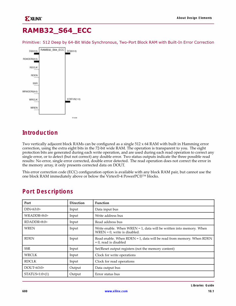
About Design Elements
RAMB32_S64_ECC
Primitive: 512 Deep by 64-Bit Wide Synchronous, Two-Port Block RAM with Built-In Error Correction
IntroductionTwo vertically adjacent block RAMs can be configured as a single 512 x 64 RAM with built in Hamming errorcorrection, using the extra eight bits in the 72-bit wide RAM. The operation is transparent to you. The eightprotection bits are generated during each write operation, and are used during each read operation to correct anysingle error, or to detect (but not correct) any double error. Two status outputs indicate the three possible readresults: No error, single error corrected, double error detected. The read operation does not correct the error inthe memory array, it only presents corrected data on DOUT.
This error correction code (ECC) configuration option is available with any block RAM pair, but cannot use theone block RAM immediately above or below the Virtex®-4 PowerPC®™ blocks.
Port DescriptionsPort Direction Function
DIN<63:0> Input Data input bus
WRADDR<8:0> Input Write address bus
RDADDR<8:0> Input Read address bus
WREN Input Write enable. When WREN = 1, data will be written into memory. WhenWREN = 0, write is disabled.
RDEN Input Read enable. When RDEN = 1, data will be read from memory. When RDEN= 0, read is disabled
SSR Input Set/Reset output registers (not the memory content)
WRCLK Input Clock for write operations
RDCLK Input Clock for read operations
DOUT<63:0> Output Data output bus
STATUS<1:0>(1) Output Error status bus
Libraries Guide
600 www.xilinx.com 10.1
About Design Elements
Note Hamming code implemented in the block RAM ECC logic detects one of three conditions: nodetectable error, single-bit error detected and corrected on DOUT (but not corrected in the memory), anddouble-bit error detected without correction. The result of STATUS<1:0> indicates these three conditions.
STATUS[1:0] Function
0 No bit error.
1 Single-bit error. The block RAM ECC macro detects and automatically corrects a single-bit error.
10 Double-bit error. The block RAM ECC macro detects a double-bit error.
11 Indeterminate state. The Hamming code implemented in the block RAM ECC cannot generate apredictable status if STATUS<1:0> is equal to three. Designers must ensure that the data has atmost double-bit errors for the STATUS<1:0> to generate the proper indicator.
Design Entry MethodThis design element can be used in schematics.
Available AttributesAttribute Type Allowed Values Default Description
DO_REG Integer 0 or 1 0 Optional output registers on A port .
SIM_COLLISION_CHECK
String “ALL”, "NONE","WARNING_ ONLY" or"GENERATE_X_ONLY”
"ALL” Collision check enable for the allowedvalue.
For More Information• See the Virtex-4 User Guide.
• See the Virtex-4 Data Sheets.
Libraries Guide
10.1 www.xilinx.com 601
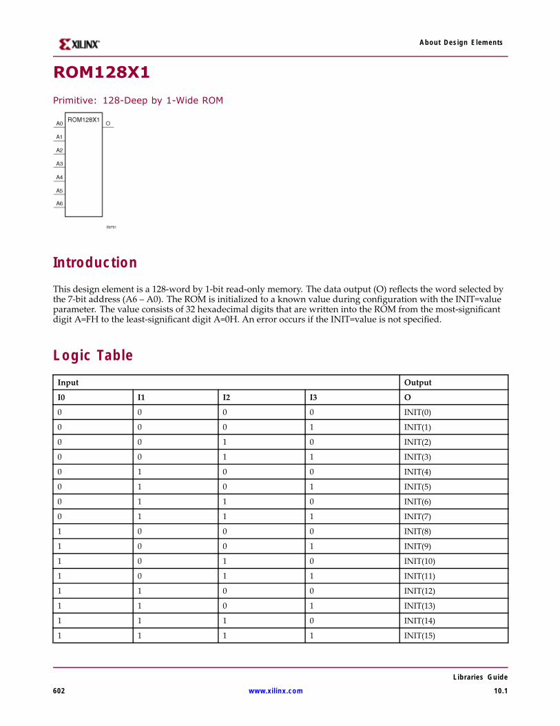
About Design Elements
ROM128X1
Primitive: 128-Deep by 1-Wide ROM
IntroductionThis design element is a 128-word by 1-bit read-only memory. The data output (O) reflects the word selected bythe 7-bit address (A6 – A0). The ROM is initialized to a known value during configuration with the INIT=valueparameter. The value consists of 32 hexadecimal digits that are written into the ROM from the most-significantdigit A=FH to the least-significant digit A=0H. An error occurs if the INIT=value is not specified.
Logic TableInput Output
I0 I1 I2 I3 O
0 0 0 0 INIT(0)
0 0 0 1 INIT(1)
0 0 1 0 INIT(2)
0 0 1 1 INIT(3)
0 1 0 0 INIT(4)
0 1 0 1 INIT(5)
0 1 1 0 INIT(6)
0 1 1 1 INIT(7)
1 0 0 0 INIT(8)
1 0 0 1 INIT(9)
1 0 1 0 INIT(10)
1 0 1 1 INIT(11)
1 1 0 0 INIT(12)
1 1 0 1 INIT(13)
1 1 1 0 INIT(14)
1 1 1 1 INIT(15)
Libraries Guide
602 www.xilinx.com 10.1

About Design Elements
Design Entry MethodThis design element can be used in schematics.
Available AttributesAttribute Type Allowed Values Default Description
INIT Hexadecimal Any 128-Bit Value All zeros Specifies the contents of the ROM.
For More Information• See the Virtex-4 User Guide.
• See the Virtex-4 Data Sheets.
Libraries Guide
10.1 www.xilinx.com 603

About Design Elements
ROM16X1
Primitive: 16-Deep by 1-Wide ROM
IntroductionThis design element is a 16-word by 1-bit read-only memory. The data output (O) reflects the word selected bythe 4-bit address (A3 – A0). The ROM is initialized to a known value during configuration with the INIT=valueparameter. The value consists of four hexadecimal digits that are written into the ROM from the most-significantdigit A=FH to the least-significant digit A=0H. For example, the INIT=10A7 parameter produces the data stream:0001 0000 1010 0111 An error occurs if the INIT=value is not specified.
Logic TableInput Output
I0 I1 I2 I3 O
0 0 0 0 INIT(0)
0 0 0 1 INIT(1)
0 0 1 0 INIT(2)
0 0 1 1 INIT(3)
0 1 0 0 INIT(4)
0 1 0 1 INIT(5)
0 1 1 0 INIT(6)
0 1 1 1 INIT(7)
1 0 0 0 INIT(8)
1 0 0 1 INIT(9)
1 0 1 0 INIT(10)
1 0 1 1 INIT(11)
1 1 0 0 INIT(12)
1 1 0 1 INIT(13)
1 1 1 0 INIT(14)
1 1 1 1 INIT(15)
Libraries Guide
604 www.xilinx.com 10.1
About Design Elements
Design Entry MethodThis design element can be used in schematics.
Available AttributesAttribute Type Allowed Values Default Description
INIT Hexadecimal Any 16-Bit Value All zeros Specifies the contents of the ROM.
For More Information• See the Virtex-4 User Guide.
• See the Virtex-4 Data Sheets.
Libraries Guide
10.1 www.xilinx.com 605
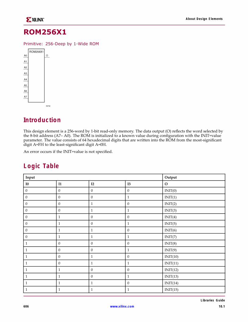
About Design Elements
ROM256X1
Primitive: 256-Deep by 1-Wide ROM
IntroductionThis design element is a 256-word by 1-bit read-only memory. The data output (O) reflects the word selected bythe 8-bit address (A7– A0). The ROM is initialized to a known value during configuration with the INIT=valueparameter. The value consists of 64 hexadecimal digits that are written into the ROM from the most-significantdigit A=FH to the least-significant digit A=0H.
An error occurs if the INIT=value is not specified.
Logic TableInput Output
I0 I1 I2 I3 O
0 0 0 0 INIT(0)
0 0 0 1 INIT(1)
0 0 1 0 INIT(2)
0 0 1 1 INIT(3)
0 1 0 0 INIT(4)
0 1 0 1 INIT(5)
0 1 1 0 INIT(6)
0 1 1 1 INIT(7)
1 0 0 0 INIT(8)
1 0 0 1 INIT(9)
1 0 1 0 INIT(10)
1 0 1 1 INIT(11)
1 1 0 0 INIT(12)
1 1 0 1 INIT(13)
1 1 1 0 INIT(14)
1 1 1 1 INIT(15)
Libraries Guide
606 www.xilinx.com 10.1

About Design Elements
Design Entry MethodThis design element can be used in schematics.
Available AttributesAttribute Type Allowed Values Default Description
INIT Hexadecimal Any 256-Bit Value All zeros Specifies the contents of the ROM.
For More Information• See the Virtex-4 User Guide.
• See the Virtex-4 Data Sheets.
Libraries Guide
10.1 www.xilinx.com 607
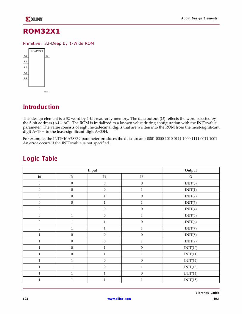
About Design Elements
ROM32X1
Primitive: 32-Deep by 1-Wide ROM
IntroductionThis design element is a 32-word by 1-bit read-only memory. The data output (O) reflects the word selected bythe 5-bit address (A4 – A0). The ROM is initialized to a known value during configuration with the INIT=valueparameter. The value consists of eight hexadecimal digits that are written into the ROM from the most-significantdigit A=1FH to the least-significant digit A=00H.
For example, the INIT=10A78F39 parameter produces the data stream: 0001 0000 1010 0111 1000 1111 0011 1001An error occurs if the INIT=value is not specified.
Logic TableInput Output
I0 I1 I2 I3 O
0 0 0 0 INIT(0)
0 0 0 1 INIT(1)
0 0 1 0 INIT(2)
0 0 1 1 INIT(3)
0 1 0 0 INIT(4)
0 1 0 1 INIT(5)
0 1 1 0 INIT(6)
0 1 1 1 INIT(7)
1 0 0 0 INIT(8)
1 0 0 1 INIT(9)
1 0 1 0 INIT(10)
1 0 1 1 INIT(11)
1 1 0 0 INIT(12)
1 1 0 1 INIT(13)
1 1 1 0 INIT(14)
1 1 1 1 INIT(15)
Libraries Guide
608 www.xilinx.com 10.1
About Design Elements
Design Entry MethodThis design element can be used in schematics.
Available AttributesAttribute Type Allowed Values Default Description
INIT Hexadecimal Any 32-Bit Value All zeros Specifies the contents of the ROM.
For More Information• See the Virtex-4 User Guide.
• See the Virtex-4 Data Sheets.
Libraries Guide
10.1 www.xilinx.com 609
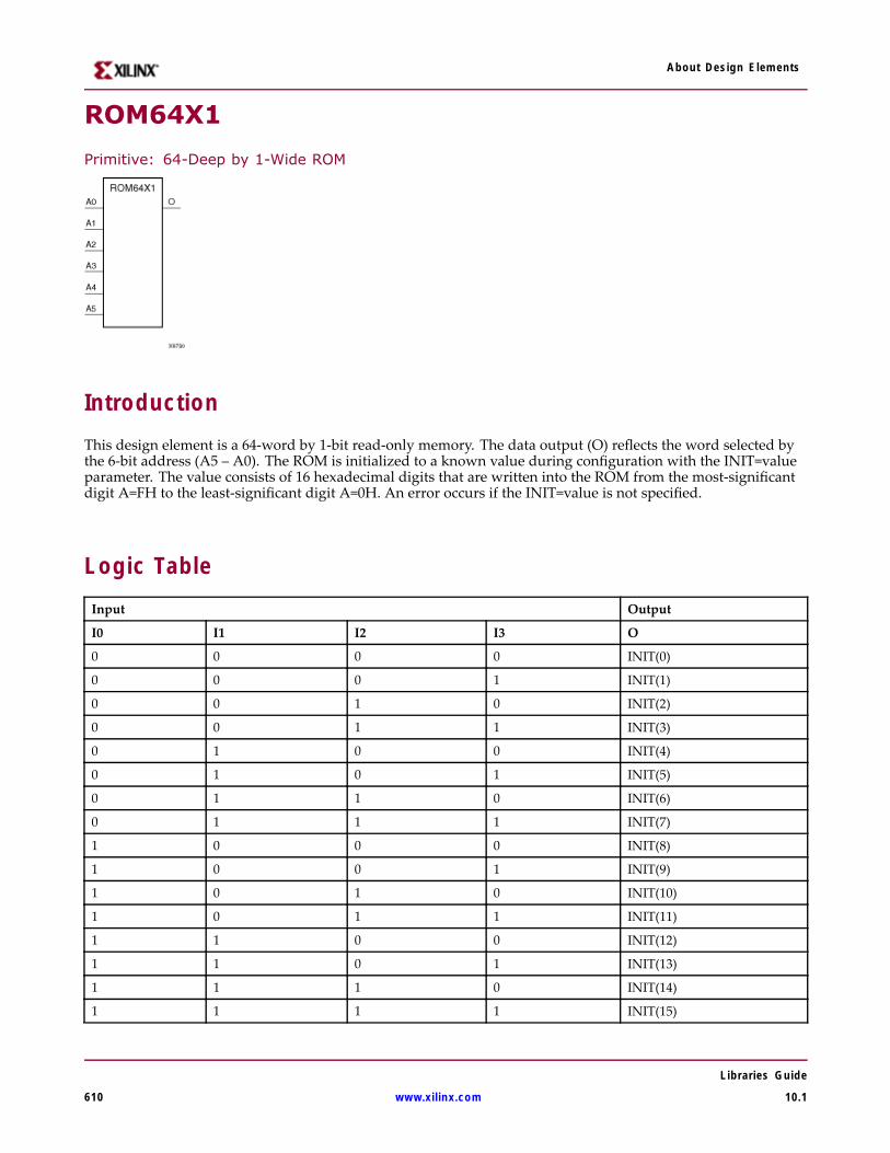
About Design Elements
ROM64X1
Primitive: 64-Deep by 1-Wide ROM
IntroductionThis design element is a 64-word by 1-bit read-only memory. The data output (O) reflects the word selected bythe 6-bit address (A5 – A0). The ROM is initialized to a known value during configuration with the INIT=valueparameter. The value consists of 16 hexadecimal digits that are written into the ROM from the most-significantdigit A=FH to the least-significant digit A=0H. An error occurs if the INIT=value is not specified.
Logic TableInput Output
I0 I1 I2 I3 O
0 0 0 0 INIT(0)
0 0 0 1 INIT(1)
0 0 1 0 INIT(2)
0 0 1 1 INIT(3)
0 1 0 0 INIT(4)
0 1 0 1 INIT(5)
0 1 1 0 INIT(6)
0 1 1 1 INIT(7)
1 0 0 0 INIT(8)
1 0 0 1 INIT(9)
1 0 1 0 INIT(10)
1 0 1 1 INIT(11)
1 1 0 0 INIT(12)
1 1 0 1 INIT(13)
1 1 1 0 INIT(14)
1 1 1 1 INIT(15)
Libraries Guide
610 www.xilinx.com 10.1

About Design Elements
Design Entry MethodThis design element can be used in schematics.
Available AttributesAttribute Type Allowed Values Default Description
INIT Hexadecimal Any 64-Bit Value All zeros Specifies the contents of the ROM.
For More Information• See the Virtex-4 User Guide.
• See the Virtex-4 Data Sheets.
Libraries Guide
10.1 www.xilinx.com 611
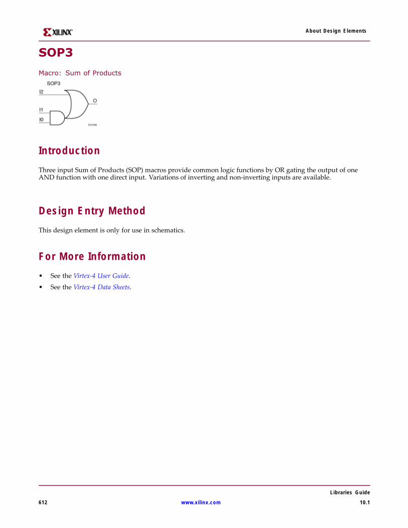
About Design Elements
SOP3
Macro: Sum of Products
IntroductionThree input Sum of Products (SOP) macros provide common logic functions by OR gating the output of oneAND function with one direct input. Variations of inverting and non-inverting inputs are available.
Design Entry MethodThis design element is only for use in schematics.
For More Information• See the Virtex-4 User Guide.
• See the Virtex-4 Data Sheets.
Libraries Guide
612 www.xilinx.com 10.1

About Design Elements
SOP3B1A
Macro: Sum of Products
IntroductionThree input Sum of Products (SOP) macros provide common logic functions by OR gating the output of oneAND function with one direct input. Variations of inverting and non-inverting inputs are available.
Design Entry MethodThis design element is only for use in schematics.
For More Information• See the Virtex-4 User Guide.
• See the Virtex-4 Data Sheets.
Libraries Guide
10.1 www.xilinx.com 613

About Design Elements
SOP3B1B
Macro: Sum of Products
IntroductionThree input Sum of Products (SOP) macros provide common logic functions by OR gating the output of oneAND function with one direct input. Variations of inverting and non-inverting inputs are available.
Design Entry MethodThis design element is only for use in schematics.
For More Information• See the Virtex-4 User Guide.
• See the Virtex-4 Data Sheets.
Libraries Guide
614 www.xilinx.com 10.1

About Design Elements
SOP3B2A
Macro: Sum of Products
IntroductionThree input Sum of Products (SOP) macros provide common logic functions by OR gating the output of oneAND function with one direct input. Variations of inverting and non-inverting inputs are available.
Design Entry MethodThis design element is only for use in schematics.
For More Information• See the Virtex-4 User Guide.
• See the Virtex-4 Data Sheets.
Libraries Guide
10.1 www.xilinx.com 615

About Design Elements
SOP3B2B
Macro: Sum of Products
IntroductionThree input Sum of Products (SOP) macros provide common logic functions by OR gating the output of oneAND function with one direct input. Variations of inverting and non-inverting inputs are available.
Design Entry MethodThis design element is only for use in schematics.
For More Information• See the Virtex-4 User Guide.
• See the Virtex-4 Data Sheets.
Libraries Guide
616 www.xilinx.com 10.1
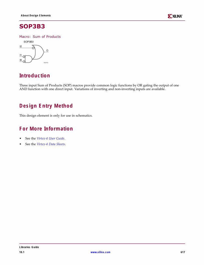
About Design Elements
SOP3B3
Macro: Sum of Products
IntroductionThree input Sum of Products (SOP) macros provide common logic functions by OR gating the output of oneAND function with one direct input. Variations of inverting and non-inverting inputs are available.
Design Entry MethodThis design element is only for use in schematics.
For More Information• See the Virtex-4 User Guide.
• See the Virtex-4 Data Sheets.
Libraries Guide
10.1 www.xilinx.com 617
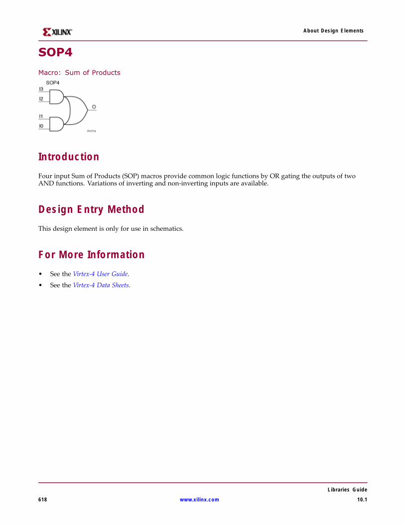
About Design Elements
SOP4
Macro: Sum of Products
IntroductionFour input Sum of Products (SOP) macros provide common logic functions by OR gating the outputs of twoAND functions. Variations of inverting and non-inverting inputs are available.
Design Entry MethodThis design element is only for use in schematics.
For More Information• See the Virtex-4 User Guide.
• See the Virtex-4 Data Sheets.
Libraries Guide
618 www.xilinx.com 10.1
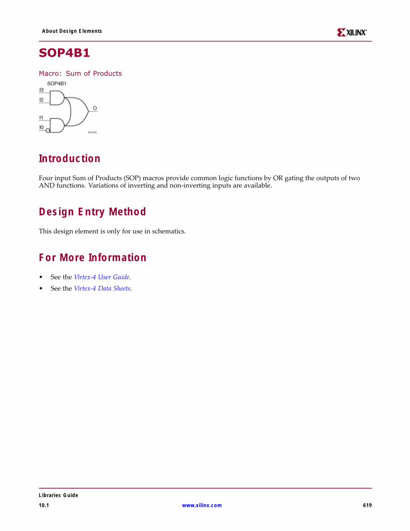
About Design Elements
SOP4B1
Macro: Sum of Products
IntroductionFour input Sum of Products (SOP) macros provide common logic functions by OR gating the outputs of twoAND functions. Variations of inverting and non-inverting inputs are available.
Design Entry MethodThis design element is only for use in schematics.
For More Information• See the Virtex-4 User Guide.
• See the Virtex-4 Data Sheets.
Libraries Guide
10.1 www.xilinx.com 619
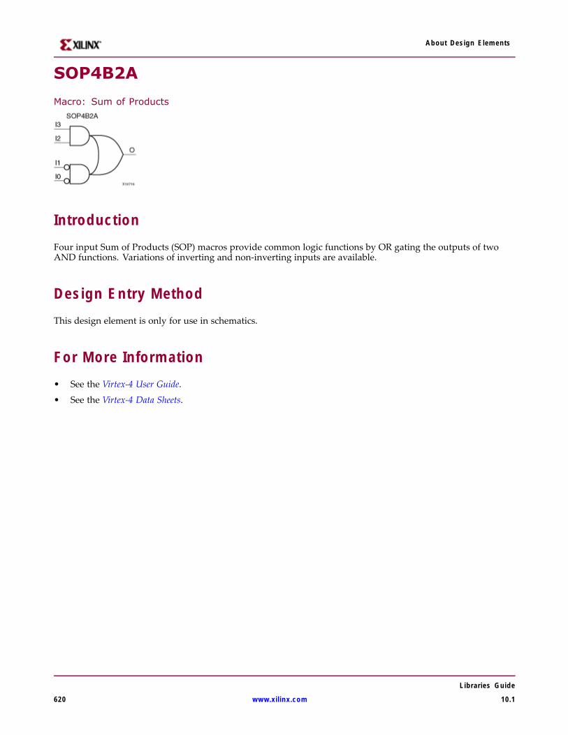
About Design Elements
SOP4B2A
Macro: Sum of Products
IntroductionFour input Sum of Products (SOP) macros provide common logic functions by OR gating the outputs of twoAND functions. Variations of inverting and non-inverting inputs are available.
Design Entry MethodThis design element is only for use in schematics.
For More Information• See the Virtex-4 User Guide.
• See the Virtex-4 Data Sheets.
Libraries Guide
620 www.xilinx.com 10.1

About Design Elements
SOP4B2B
Macro: Sum of Products
IntroductionFour input Sum of Products (SOP) macros provide common logic functions by OR gating the outputs of twoAND functions. Variations of inverting and non-inverting inputs are available.
Design Entry MethodThis design element is only for use in schematics.
For More Information• See the Virtex-4 User Guide.
• See the Virtex-4 Data Sheets.
Libraries Guide
10.1 www.xilinx.com 621
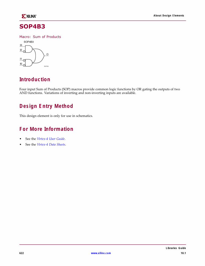
About Design Elements
SOP4B3
Macro: Sum of Products
IntroductionFour input Sum of Products (SOP) macros provide common logic functions by OR gating the outputs of twoAND functions. Variations of inverting and non-inverting inputs are available.
Design Entry MethodThis design element is only for use in schematics.
For More Information• See the Virtex-4 User Guide.
• See the Virtex-4 Data Sheets.
Libraries Guide
622 www.xilinx.com 10.1

About Design Elements
SOP4B4
Macro: Sum of Products
IntroductionFour input Sum of Products (SOP) macros provide common logic functions by OR gating the outputs of twoAND functions. Variations of inverting and non-inverting inputs are available.
Design Entry MethodThis design element is only for use in schematics.
For More Information• See the Virtex-4 User Guide.
• See the Virtex-4 Data Sheets.
Libraries Guide
10.1 www.xilinx.com 623
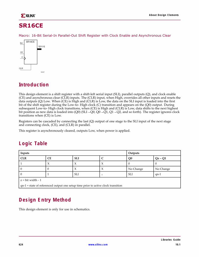
About Design Elements
SR16CE
Macro: 16-Bit Serial-In Parallel-Out Shift Register with Clock Enable and Asynchronous Clear
IntroductionThis design element is a shift register with a shift-left serial input (SLI), parallel outputs (Q), and clock enable(CE) and asynchronous clear (CLR) inputs. The (CLR) input, when High, overrides all other inputs and resets thedata outputs (Q) Low. When (CE) is High and (CLR) is Low, the data on the SLI input is loaded into the firstbit of the shift register during the Low-to- High clock (C) transition and appears on the (Q0) output. Duringsubsequent Low-to- High clock transitions, when (CE) is High and (CLR) is Low, data shifts to the next highestbit position as new data is loaded into (Q0) (SLI→Q0, Q0→Q1, Q1→Q2, and so forth). The register ignores clocktransitions when (CE) is Low.
Registers can be cascaded by connecting the last (Q) output of one stage to the SLI input of the next stageand connecting clock, (CE), and (CLR) in parallel.
This register is asynchronously cleared, outputs Low, when power is applied.
Logic TableInputs Outputs
CLR CE SLI C Q0 Qz – Q1
1 X X X 0 0
0 0 X X No Change No Change
0 1 SLI ↑ SLI qn-1
z = bit width - 1
qn-1 = state of referenced output one setup time prior to active clock transition
Design Entry MethodThis design element is only for use in schematics.
Libraries Guide
624 www.xilinx.com 10.1

About Design Elements
For More Information• See the Virtex-4 User Guide.
• See the Virtex-4 Data Sheets.
Libraries Guide
10.1 www.xilinx.com 625
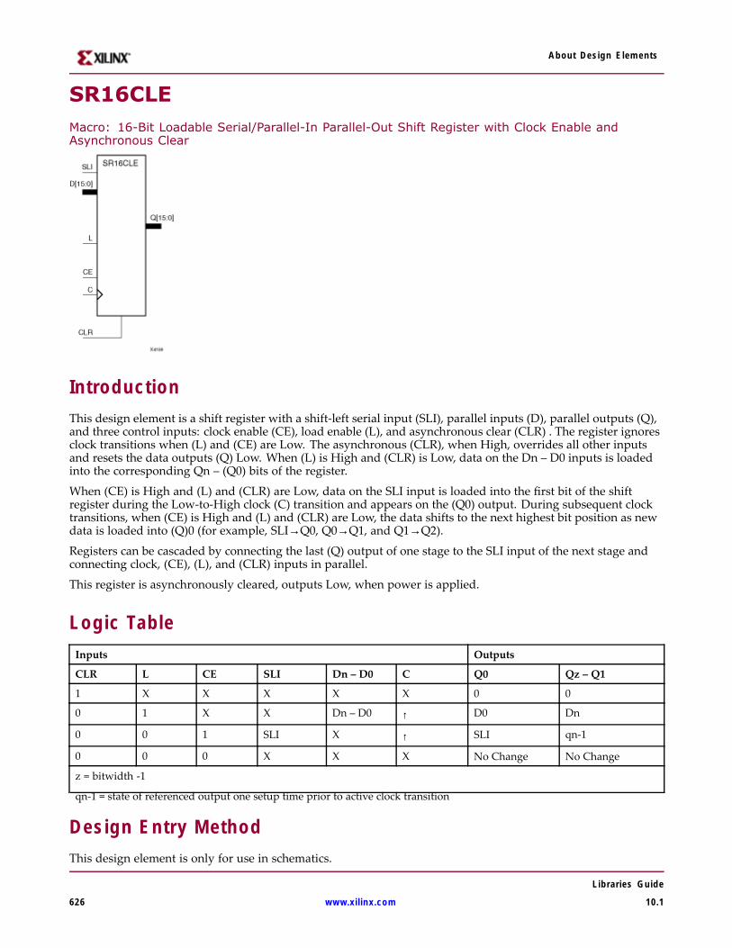
About Design Elements
SR16CLEMacro: 16-Bit Loadable Serial/Parallel-In Parallel-Out Shift Register with Clock Enable andAsynchronous Clear
IntroductionThis design element is a shift register with a shift-left serial input (SLI), parallel inputs (D), parallel outputs (Q),and three control inputs: clock enable (CE), load enable (L), and asynchronous clear (CLR) . The register ignoresclock transitions when (L) and (CE) are Low. The asynchronous (CLR), when High, overrides all other inputsand resets the data outputs (Q) Low. When (L) is High and (CLR) is Low, data on the Dn – D0 inputs is loadedinto the corresponding Qn – (Q0) bits of the register.
When (CE) is High and (L) and (CLR) are Low, data on the SLI input is loaded into the first bit of the shiftregister during the Low-to-High clock (C) transition and appears on the (Q0) output. During subsequent clocktransitions, when (CE) is High and (L) and (CLR) are Low, the data shifts to the next highest bit position as newdata is loaded into (Q)0 (for example, SLI→Q0, Q0→Q1, and Q1→Q2).
Registers can be cascaded by connecting the last (Q) output of one stage to the SLI input of the next stage andconnecting clock, (CE), (L), and (CLR) inputs in parallel.
This register is asynchronously cleared, outputs Low, when power is applied.
Logic TableInputs Outputs
CLR L CE SLI Dn – D0 C Q0 Qz – Q1
1 X X X X X 0 0
0 1 X X Dn – D0 ↑ D0 Dn
0 0 1 SLI X ↑ SLI qn-1
0 0 0 X X X No Change No Change
z = bitwidth -1
qn-1 = state of referenced output one setup time prior to active clock transition
Design Entry MethodThis design element is only for use in schematics.
Libraries Guide
626 www.xilinx.com 10.1

About Design Elements
For More Information• See the Virtex-4 User Guide.
• See the Virtex-4 Data Sheets.
Libraries Guide
10.1 www.xilinx.com 627
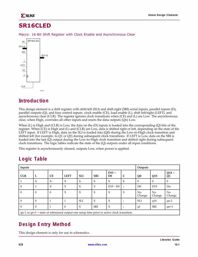
About Design Elements
SR16CLEDMacro: 16-Bit Shift Register with Clock Enable and Asynchronous Clear
IntroductionThis design element is a shift register with shift-left (SLI) and shift-right (SRI) serial inputs, parallel inputs (D),parallel outputs (Q), and four control inputs: clock enable (CE), load enable (L), shift left/right (LEFT), andasynchronous clear (CLR). The register ignores clock transitions when (CE) and (L) are Low. The asynchronousclear, when High, overrides all other inputs and resets the data outputs (Qn) Low.
When (L) is High and (CLR) is Low, the data on the (D) inputs is loaded into the corresponding (Q) bits of theregister. When (CE) is High and (L) and (CLR) are Low, data is shifted right or left, depending on the state of theLEFT input. If LEFT is High, data on the SLI is loaded into (Q0) during the Low-to-High clock transition andshifted left (for example, to Q1 or Q2) during subsequent clock transitions. If LEFT is Low, data on the SRI isloaded into the last (Q) output during the Low-to-High clock transition and shifted right during subsequentclock transitions. The logic tables indicate the state of the (Q) outputs under all input conditions.
This register is asynchronously cleared, outputs Low, when power is applied.
Logic TableInputs Outputs
CLR L CE LEFT SLI SRID15 –D0 C Q0 Q15
Q14 –Q1
1 X X X X X X X 0 0 0
0 1 X X X X D15 –D0 ↑ D0 D15 Dn
0 0 0 X X X X X NoChange
NoChange
NoChange
0 0 1 1 SLI X X ↑ SLI q14 qn-1
0 0 1 0 X SRI X ↑ q1 SRI qn+1
qn-1 or qn+1 = state of referenced output one setup time prior to active clock transition.
Design Entry MethodThis design element is only for use in schematics.
Libraries Guide
628 www.xilinx.com 10.1

About Design Elements
For More Information• See the Virtex-4 User Guide.
• See the Virtex-4 Data Sheets.
Libraries Guide
10.1 www.xilinx.com 629

About Design Elements
SR16RE
Macro: 16-Bit Serial-In Parallel-Out Shift Register with Clock Enable and Synchronous Reset
IntroductionThis design element is a shift register with shift-left serial input (SLI), parallel outputs (Qn), clock enable (CE),and synchronous reset (R) inputs. The R input, when High, overrides all other inputs during the Low-to-Highclock (C) transition and resets the data outputs (Q) Low.
When (CE) is High and (R) is Low, the data on the (SLI) is loaded into the first bit of the shift register duringthe Low-to-High clock (C) transition and appears on the (Q0) output. During subsequent Low-to-High clocktransitions, when (CE) is High and R is Low, data shifts to the next highest bit position as new data is loaded into(Q0) (for example, SLI→Q0, Q0→Q1, and Q1→Q2). The register ignores clock transitions when (CE) is Low.
Registers can be cascaded by connecting the last (Q) output of one stage to the SLI input of the next stage andconnecting clock, (CE), and (R) in parallel.
This register is asynchronously cleared, outputs Low, when power is applied.
Logic TableInputs Outputs
R CE SLI C Q0 Qz – Q1
1 X X ↑ 0 0
0 0 X X No Change No Change
0 1 SLI ↑ SLI qn-1
z = bitwidth -1
qn-1 = state of referenced output one setup time prior to active clock transition
Design Entry MethodThis design element is only for use in schematics.
Libraries Guide
630 www.xilinx.com 10.1

About Design Elements
For More Information• See the Virtex-4 User Guide.
• See the Virtex-4 Data Sheets.
Libraries Guide
10.1 www.xilinx.com 631
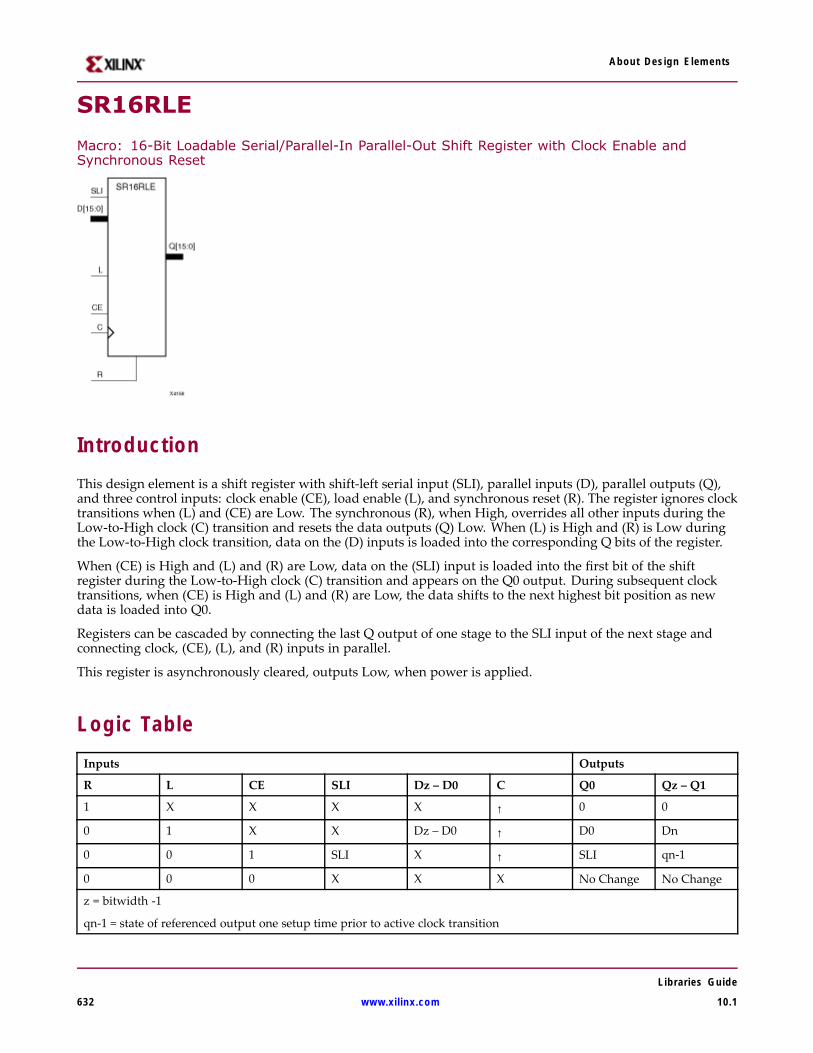
About Design Elements
SR16RLE
Macro: 16-Bit Loadable Serial/Parallel-In Parallel-Out Shift Register with Clock Enable andSynchronous Reset
IntroductionThis design element is a shift register with shift-left serial input (SLI), parallel inputs (D), parallel outputs (Q),and three control inputs: clock enable (CE), load enable (L), and synchronous reset (R). The register ignores clocktransitions when (L) and (CE) are Low. The synchronous (R), when High, overrides all other inputs during theLow-to-High clock (C) transition and resets the data outputs (Q) Low. When (L) is High and (R) is Low duringthe Low-to-High clock transition, data on the (D) inputs is loaded into the corresponding Q bits of the register.
When (CE) is High and (L) and (R) are Low, data on the (SLI) input is loaded into the first bit of the shiftregister during the Low-to-High clock (C) transition and appears on the Q0 output. During subsequent clocktransitions, when (CE) is High and (L) and (R) are Low, the data shifts to the next highest bit position as newdata is loaded into Q0.
Registers can be cascaded by connecting the last Q output of one stage to the SLI input of the next stage andconnecting clock, (CE), (L), and (R) inputs in parallel.
This register is asynchronously cleared, outputs Low, when power is applied.
Logic TableInputs Outputs
R L CE SLI Dz – D0 C Q0 Qz – Q1
1 X X X X ↑ 0 0
0 1 X X Dz – D0 ↑ D0 Dn
0 0 1 SLI X ↑ SLI qn-1
0 0 0 X X X No Change No Change
z = bitwidth -1
qn-1 = state of referenced output one setup time prior to active clock transition
Libraries Guide
632 www.xilinx.com 10.1

About Design Elements
Design Entry MethodThis design element is only for use in schematics.
For More Information• See the Virtex-4 User Guide.
• See the Virtex-4 Data Sheets.
Libraries Guide
10.1 www.xilinx.com 633
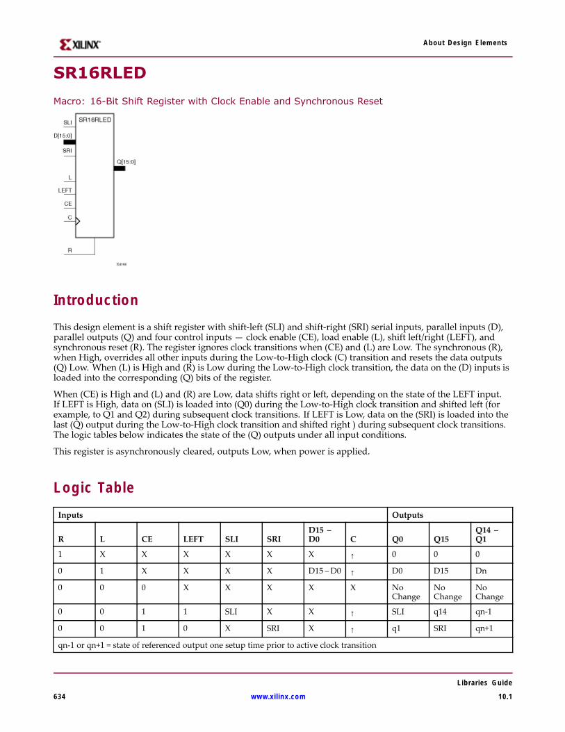
About Design Elements
SR16RLED
Macro: 16-Bit Shift Register with Clock Enable and Synchronous Reset
IntroductionThis design element is a shift register with shift-left (SLI) and shift-right (SRI) serial inputs, parallel inputs (D),parallel outputs (Q) and four control inputs — clock enable (CE), load enable (L), shift left/right (LEFT), andsynchronous reset (R). The register ignores clock transitions when (CE) and (L) are Low. The synchronous (R),when High, overrides all other inputs during the Low-to-High clock (C) transition and resets the data outputs(Q) Low. When (L) is High and (R) is Low during the Low-to-High clock transition, the data on the (D) inputs isloaded into the corresponding (Q) bits of the register.
When (CE) is High and (L) and (R) are Low, data shifts right or left, depending on the state of the LEFT input.If LEFT is High, data on (SLI) is loaded into (Q0) during the Low-to-High clock transition and shifted left (forexample, to Q1 and Q2) during subsequent clock transitions. If LEFT is Low, data on the (SRI) is loaded into thelast (Q) output during the Low-to-High clock transition and shifted right ) during subsequent clock transitions.The logic tables below indicates the state of the (Q) outputs under all input conditions.
This register is asynchronously cleared, outputs Low, when power is applied.
Logic TableInputs Outputs
R L CE LEFT SLI SRID15 –D0 C Q0 Q15
Q14 –Q1
1 X X X X X X ↑ 0 0 0
0 1 X X X X D15 –D0 ↑ D0 D15 Dn
0 0 0 X X X X X NoChange
NoChange
NoChange
0 0 1 1 SLI X X ↑ SLI q14 qn-1
0 0 1 0 X SRI X ↑ q1 SRI qn+1
qn-1 or qn+1 = state of referenced output one setup time prior to active clock transition
Libraries Guide
634 www.xilinx.com 10.1

About Design Elements
Design Entry MethodThis design element is only for use in schematics.
For More Information• See the Virtex-4 User Guide.
• See the Virtex-4 Data Sheets.
Libraries Guide
10.1 www.xilinx.com 635

About Design Elements
SR4CE
Macro: 4-Bit Serial-In Parallel-Out Shift Register with Clock Enable and Asynchronous Clear
IntroductionThis design element is a shift register with a shift-left serial input (SLI), parallel outputs (Q), and clock enable(CE) and asynchronous clear (CLR) inputs. The (CLR) input, when High, overrides all other inputs and resets thedata outputs (Q) Low. When (CE) is High and (CLR) is Low, the data on the SLI input is loaded into the firstbit of the shift register during the Low-to- High clock (C) transition and appears on the (Q0) output. Duringsubsequent Low-to- High clock transitions, when (CE) is High and (CLR) is Low, data shifts to the next highestbit position as new data is loaded into (Q0) (SLI→Q0, Q0→Q1, Q1→Q2, and so forth). The register ignores clocktransitions when (CE) is Low.
Registers can be cascaded by connecting the last (Q) output of one stage to the SLI input of the next stageand connecting clock, (CE), and (CLR) in parallel.
This register is asynchronously cleared, outputs Low, when power is applied.
Logic TableInputs Outputs
CLR CE SLI C Q0 Qz – Q1
1 X X X 0 0
0 0 X X No Change No Change
0 1 SLI ↑ SLI qn-1
z = bit width - 1
qn-1 = state of referenced output one setup time prior to active clock transition
Design Entry MethodThis design element is only for use in schematics.
Libraries Guide
636 www.xilinx.com 10.1

About Design Elements
For More Information• See the Virtex-4 User Guide.
• See the Virtex-4 Data Sheets.
Libraries Guide
10.1 www.xilinx.com 637
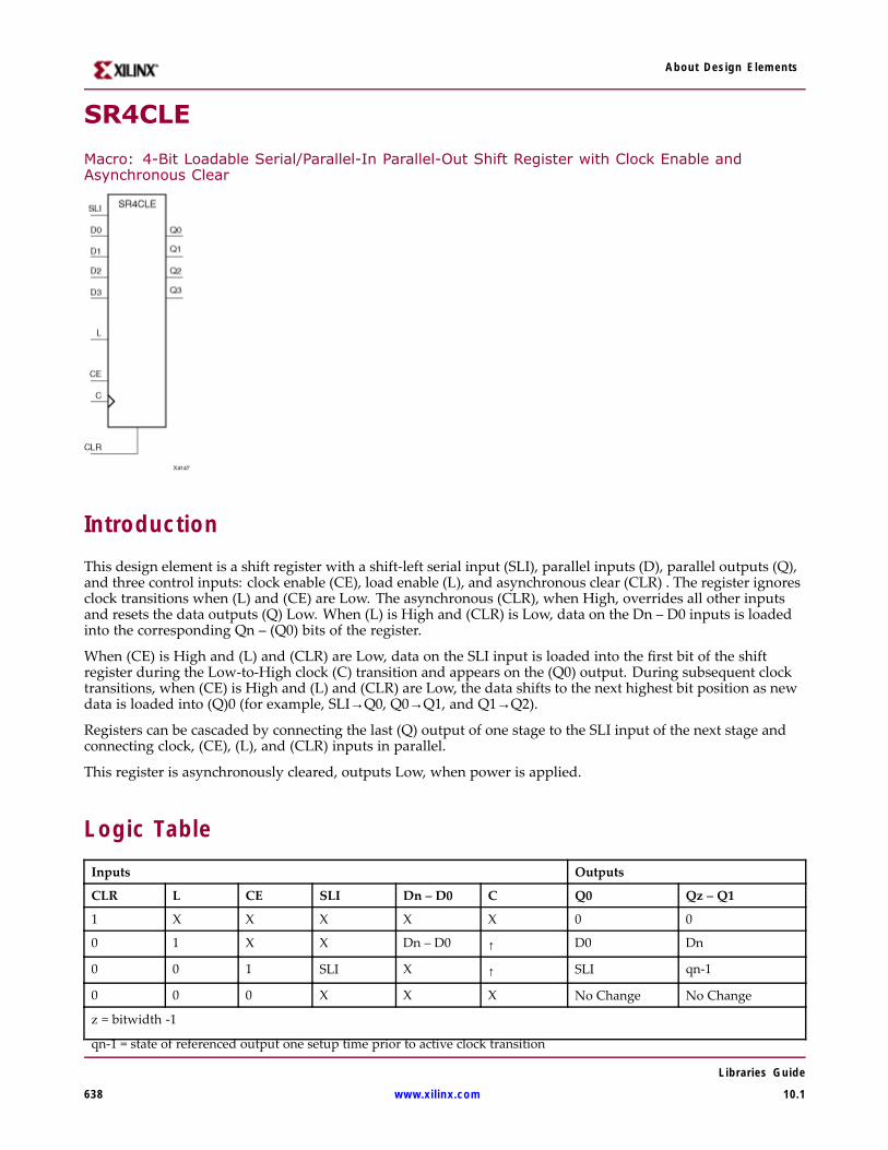
About Design Elements
SR4CLE
Macro: 4-Bit Loadable Serial/Parallel-In Parallel-Out Shift Register with Clock Enable andAsynchronous Clear
IntroductionThis design element is a shift register with a shift-left serial input (SLI), parallel inputs (D), parallel outputs (Q),and three control inputs: clock enable (CE), load enable (L), and asynchronous clear (CLR) . The register ignoresclock transitions when (L) and (CE) are Low. The asynchronous (CLR), when High, overrides all other inputsand resets the data outputs (Q) Low. When (L) is High and (CLR) is Low, data on the Dn – D0 inputs is loadedinto the corresponding Qn – (Q0) bits of the register.
When (CE) is High and (L) and (CLR) are Low, data on the SLI input is loaded into the first bit of the shiftregister during the Low-to-High clock (C) transition and appears on the (Q0) output. During subsequent clocktransitions, when (CE) is High and (L) and (CLR) are Low, the data shifts to the next highest bit position as newdata is loaded into (Q)0 (for example, SLI→Q0, Q0→Q1, and Q1→Q2).
Registers can be cascaded by connecting the last (Q) output of one stage to the SLI input of the next stage andconnecting clock, (CE), (L), and (CLR) inputs in parallel.
This register is asynchronously cleared, outputs Low, when power is applied.
Logic TableInputs Outputs
CLR L CE SLI Dn – D0 C Q0 Qz – Q1
1 X X X X X 0 0
0 1 X X Dn – D0 ↑ D0 Dn
0 0 1 SLI X ↑ SLI qn-1
0 0 0 X X X No Change No Change
z = bitwidth -1
qn-1 = state of referenced output one setup time prior to active clock transition
Libraries Guide
638 www.xilinx.com 10.1

About Design Elements
Design Entry MethodThis design element is only for use in schematics.
For More Information• See the Virtex-4 User Guide.
• See the Virtex-4 Data Sheets.
Libraries Guide
10.1 www.xilinx.com 639
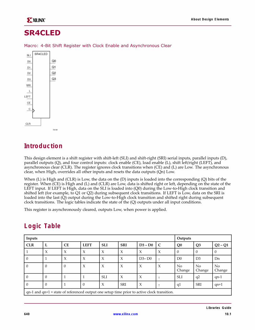
About Design Elements
SR4CLED
Macro: 4-Bit Shift Register with Clock Enable and Asynchronous Clear
IntroductionThis design element is a shift register with shift-left (SLI) and shift-right (SRI) serial inputs, parallel inputs (D),parallel outputs (Q), and four control inputs: clock enable (CE), load enable (L), shift left/right (LEFT), andasynchronous clear (CLR). The register ignores clock transitions when (CE) and (L) are Low. The asynchronousclear, when High, overrides all other inputs and resets the data outputs (Qn) Low.
When (L) is High and (CLR) is Low, the data on the (D) inputs is loaded into the corresponding (Q) bits of theregister. When (CE) is High and (L) and (CLR) are Low, data is shifted right or left, depending on the state of theLEFT input. If LEFT is High, data on the SLI is loaded into (Q0) during the Low-to-High clock transition andshifted left (for example, to Q1 or Q2) during subsequent clock transitions. If LEFT is Low, data on the SRI isloaded into the last (Q) output during the Low-to-High clock transition and shifted right during subsequentclock transitions. The logic tables indicate the state of the (Q) outputs under all input conditions.
This register is asynchronously cleared, outputs Low, when power is applied.
Logic TableInputs Outputs
CLR L CE LEFT SLI SRI D3 – D0 C Q0 Q3 Q2 – Q1
1 X X X X X X X 0 0 0
0 1 X X X X D3– D0 ↑ D0 D3 Dn
0 0 0 X X X X X NoChange
NoChange
NoChange
0 0 1 1 SLI X X ↑ SLI q2 qn-1
0 0 1 0 X SRI X ↑ q1 SRI qn+1
qn-1 and qn+1 = state of referenced output one setup time prior to active clock transition.
Libraries Guide
640 www.xilinx.com 10.1

About Design Elements
Design Entry MethodThis design element is only for use in schematics.
For More Information• See the Virtex-4 User Guide.
• See the Virtex-4 Data Sheets.
Libraries Guide
10.1 www.xilinx.com 641
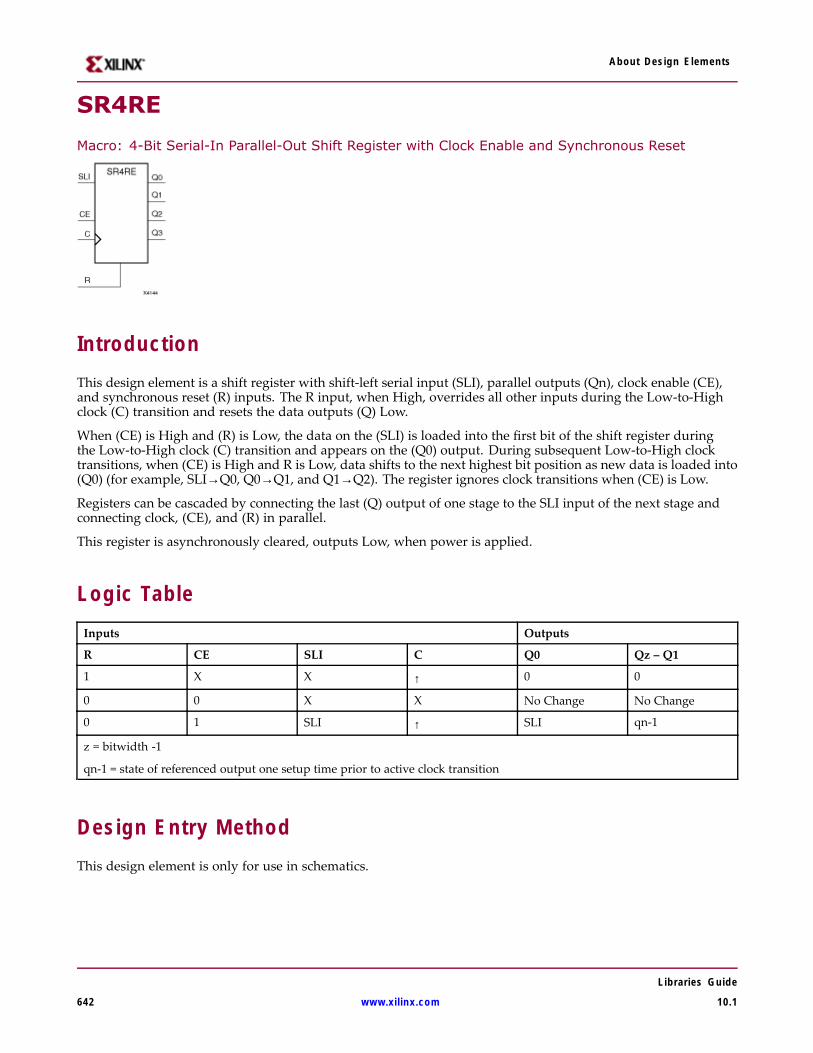
About Design Elements
SR4RE
Macro: 4-Bit Serial-In Parallel-Out Shift Register with Clock Enable and Synchronous Reset
IntroductionThis design element is a shift register with shift-left serial input (SLI), parallel outputs (Qn), clock enable (CE),and synchronous reset (R) inputs. The R input, when High, overrides all other inputs during the Low-to-Highclock (C) transition and resets the data outputs (Q) Low.
When (CE) is High and (R) is Low, the data on the (SLI) is loaded into the first bit of the shift register duringthe Low-to-High clock (C) transition and appears on the (Q0) output. During subsequent Low-to-High clocktransitions, when (CE) is High and R is Low, data shifts to the next highest bit position as new data is loaded into(Q0) (for example, SLI→Q0, Q0→Q1, and Q1→Q2). The register ignores clock transitions when (CE) is Low.
Registers can be cascaded by connecting the last (Q) output of one stage to the SLI input of the next stage andconnecting clock, (CE), and (R) in parallel.
This register is asynchronously cleared, outputs Low, when power is applied.
Logic TableInputs Outputs
R CE SLI C Q0 Qz – Q1
1 X X ↑ 0 0
0 0 X X No Change No Change
0 1 SLI ↑ SLI qn-1
z = bitwidth -1
qn-1 = state of referenced output one setup time prior to active clock transition
Design Entry MethodThis design element is only for use in schematics.
Libraries Guide
642 www.xilinx.com 10.1

About Design Elements
For More Information• See the Virtex-4 User Guide.
• See the Virtex-4 Data Sheets.
Libraries Guide
10.1 www.xilinx.com 643
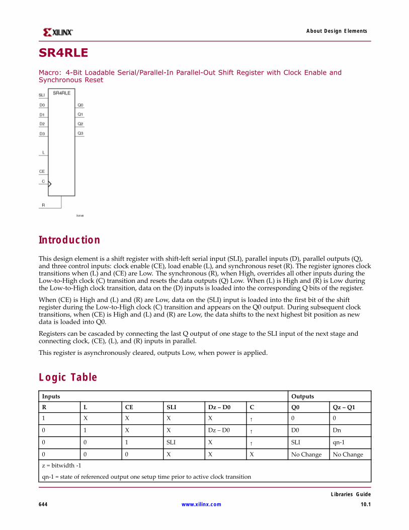
About Design Elements
SR4RLE
Macro: 4-Bit Loadable Serial/Parallel-In Parallel-Out Shift Register with Clock Enable andSynchronous Reset
IntroductionThis design element is a shift register with shift-left serial input (SLI), parallel inputs (D), parallel outputs (Q),and three control inputs: clock enable (CE), load enable (L), and synchronous reset (R). The register ignores clocktransitions when (L) and (CE) are Low. The synchronous (R), when High, overrides all other inputs during theLow-to-High clock (C) transition and resets the data outputs (Q) Low. When (L) is High and (R) is Low duringthe Low-to-High clock transition, data on the (D) inputs is loaded into the corresponding Q bits of the register.
When (CE) is High and (L) and (R) are Low, data on the (SLI) input is loaded into the first bit of the shiftregister during the Low-to-High clock (C) transition and appears on the Q0 output. During subsequent clocktransitions, when (CE) is High and (L) and (R) are Low, the data shifts to the next highest bit position as newdata is loaded into Q0.
Registers can be cascaded by connecting the last Q output of one stage to the SLI input of the next stage andconnecting clock, (CE), (L), and (R) inputs in parallel.
This register is asynchronously cleared, outputs Low, when power is applied.
Logic TableInputs Outputs
R L CE SLI Dz – D0 C Q0 Qz – Q1
1 X X X X ↑ 0 0
0 1 X X Dz – D0 ↑ D0 Dn
0 0 1 SLI X ↑ SLI qn-1
0 0 0 X X X No Change No Change
z = bitwidth -1
qn-1 = state of referenced output one setup time prior to active clock transition
Libraries Guide
644 www.xilinx.com 10.1
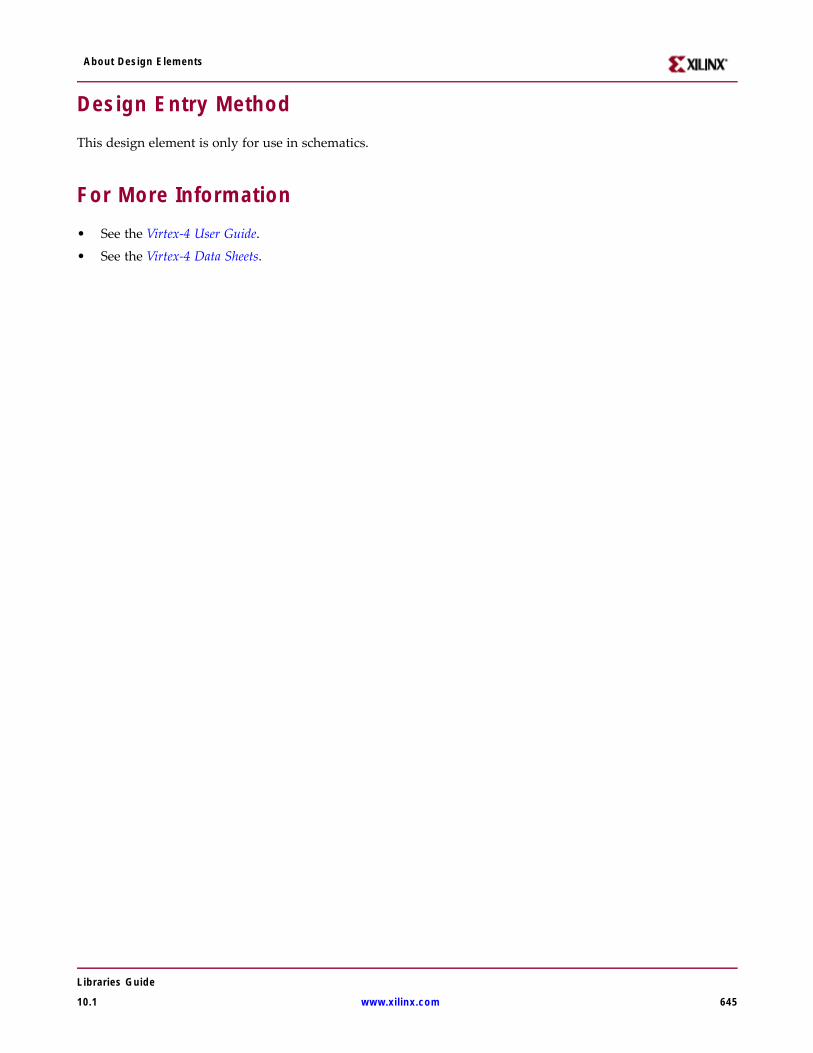
About Design Elements
Design Entry MethodThis design element is only for use in schematics.
For More Information• See the Virtex-4 User Guide.
• See the Virtex-4 Data Sheets.
Libraries Guide
10.1 www.xilinx.com 645
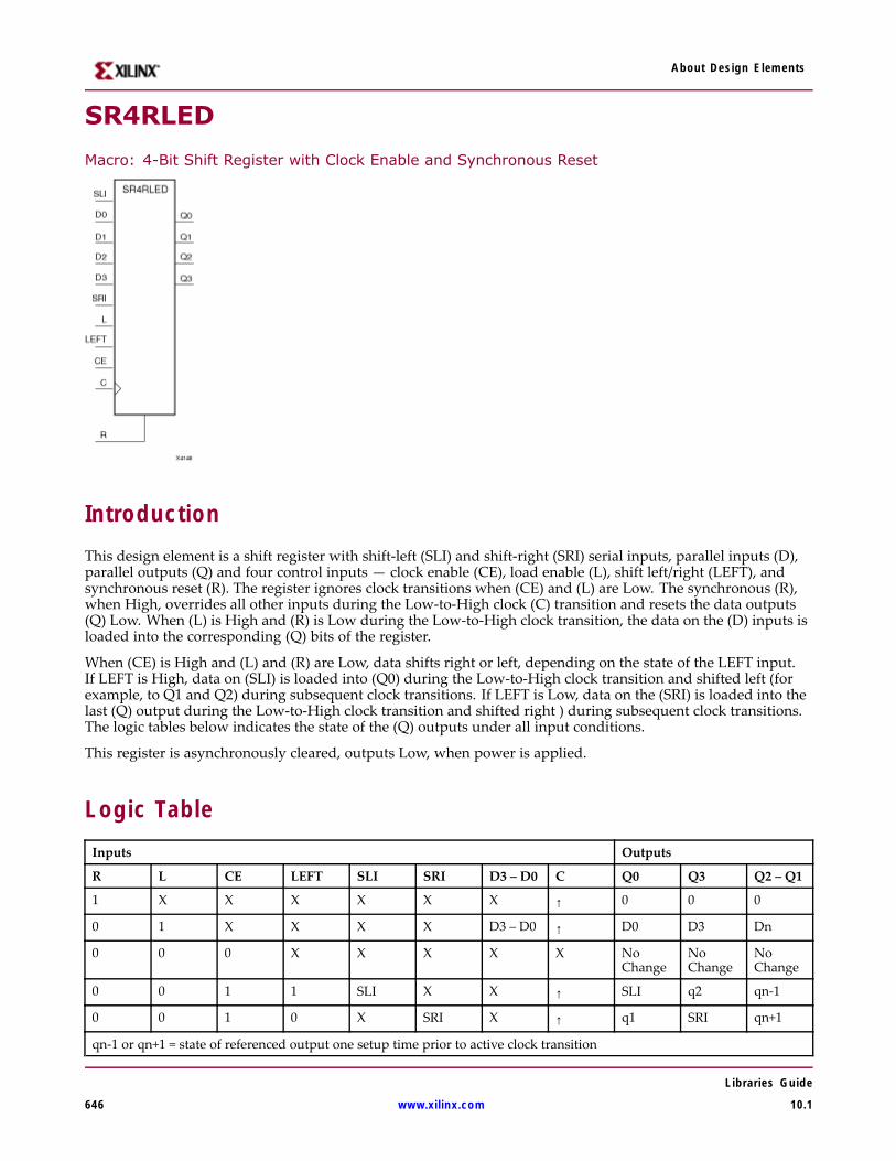
About Design Elements
SR4RLED
Macro: 4-Bit Shift Register with Clock Enable and Synchronous Reset
IntroductionThis design element is a shift register with shift-left (SLI) and shift-right (SRI) serial inputs, parallel inputs (D),parallel outputs (Q) and four control inputs — clock enable (CE), load enable (L), shift left/right (LEFT), andsynchronous reset (R). The register ignores clock transitions when (CE) and (L) are Low. The synchronous (R),when High, overrides all other inputs during the Low-to-High clock (C) transition and resets the data outputs(Q) Low. When (L) is High and (R) is Low during the Low-to-High clock transition, the data on the (D) inputs isloaded into the corresponding (Q) bits of the register.
When (CE) is High and (L) and (R) are Low, data shifts right or left, depending on the state of the LEFT input.If LEFT is High, data on (SLI) is loaded into (Q0) during the Low-to-High clock transition and shifted left (forexample, to Q1 and Q2) during subsequent clock transitions. If LEFT is Low, data on the (SRI) is loaded into thelast (Q) output during the Low-to-High clock transition and shifted right ) during subsequent clock transitions.The logic tables below indicates the state of the (Q) outputs under all input conditions.
This register is asynchronously cleared, outputs Low, when power is applied.
Logic TableInputs Outputs
R L CE LEFT SLI SRI D3 – D0 C Q0 Q3 Q2 – Q1
1 X X X X X X ↑ 0 0 0
0 1 X X X X D3 – D0 ↑ D0 D3 Dn
0 0 0 X X X X X NoChange
NoChange
NoChange
0 0 1 1 SLI X X ↑ SLI q2 qn-1
0 0 1 0 X SRI X ↑ q1 SRI qn+1
qn-1 or qn+1 = state of referenced output one setup time prior to active clock transition
Libraries Guide
646 www.xilinx.com 10.1

About Design Elements
Design Entry MethodThis design element is only for use in schematics.
For More Information• See the Virtex-4 User Guide.
• See the Virtex-4 Data Sheets.
Libraries Guide
10.1 www.xilinx.com 647
About Design Elements
SR8CE
Macro: 8-Bit Serial-In Parallel-Out Shift Register with Clock Enable and Asynchronous Clear
IntroductionThis design element is a shift register with a shift-left serial input (SLI), parallel outputs (Q), and clock enable(CE) and asynchronous clear (CLR) inputs. The (CLR) input, when High, overrides all other inputs and resets thedata outputs (Q) Low. When (CE) is High and (CLR) is Low, the data on the SLI input is loaded into the firstbit of the shift register during the Low-to- High clock (C) transition and appears on the (Q0) output. Duringsubsequent Low-to- High clock transitions, when (CE) is High and (CLR) is Low, data shifts to the next highestbit position as new data is loaded into (Q0) (SLI→Q0, Q0→Q1, Q1→Q2, and so forth). The register ignores clocktransitions when (CE) is Low.
Registers can be cascaded by connecting the last (Q) output of one stage to the SLI input of the next stageand connecting clock, (CE), and (CLR) in parallel.
This register is asynchronously cleared, outputs Low, when power is applied.
Logic TableInputs Outputs
CLR CE SLI C Q0 Qz – Q1
1 X X X 0 0
0 0 X X No Change No Change
0 1 SLI ↑ SLI qn-1
z = bit width - 1
qn-1 = state of referenced output one setup time prior to active clock transition
Design Entry MethodThis design element is only for use in schematics.
Libraries Guide
648 www.xilinx.com 10.1

About Design Elements
For More Information• See the Virtex-4 User Guide.
• See the Virtex-4 Data Sheets.
Libraries Guide
10.1 www.xilinx.com 649
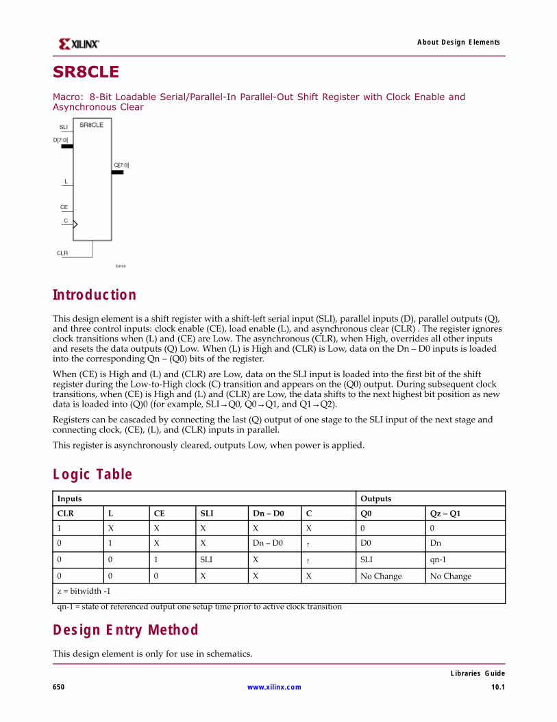
About Design Elements
SR8CLEMacro: 8-Bit Loadable Serial/Parallel-In Parallel-Out Shift Register with Clock Enable andAsynchronous Clear
IntroductionThis design element is a shift register with a shift-left serial input (SLI), parallel inputs (D), parallel outputs (Q),and three control inputs: clock enable (CE), load enable (L), and asynchronous clear (CLR) . The register ignoresclock transitions when (L) and (CE) are Low. The asynchronous (CLR), when High, overrides all other inputsand resets the data outputs (Q) Low. When (L) is High and (CLR) is Low, data on the Dn – D0 inputs is loadedinto the corresponding Qn – (Q0) bits of the register.
When (CE) is High and (L) and (CLR) are Low, data on the SLI input is loaded into the first bit of the shiftregister during the Low-to-High clock (C) transition and appears on the (Q0) output. During subsequent clocktransitions, when (CE) is High and (L) and (CLR) are Low, the data shifts to the next highest bit position as newdata is loaded into (Q)0 (for example, SLI→Q0, Q0→Q1, and Q1→Q2).
Registers can be cascaded by connecting the last (Q) output of one stage to the SLI input of the next stage andconnecting clock, (CE), (L), and (CLR) inputs in parallel.
This register is asynchronously cleared, outputs Low, when power is applied.
Logic TableInputs Outputs
CLR L CE SLI Dn – D0 C Q0 Qz – Q1
1 X X X X X 0 0
0 1 X X Dn – D0 ↑ D0 Dn
0 0 1 SLI X ↑ SLI qn-1
0 0 0 X X X No Change No Change
z = bitwidth -1
qn-1 = state of referenced output one setup time prior to active clock transition
Design Entry MethodThis design element is only for use in schematics.
Libraries Guide
650 www.xilinx.com 10.1

About Design Elements
For More Information• See the Virtex-4 User Guide.
• See the Virtex-4 Data Sheets.
Libraries Guide
10.1 www.xilinx.com 651
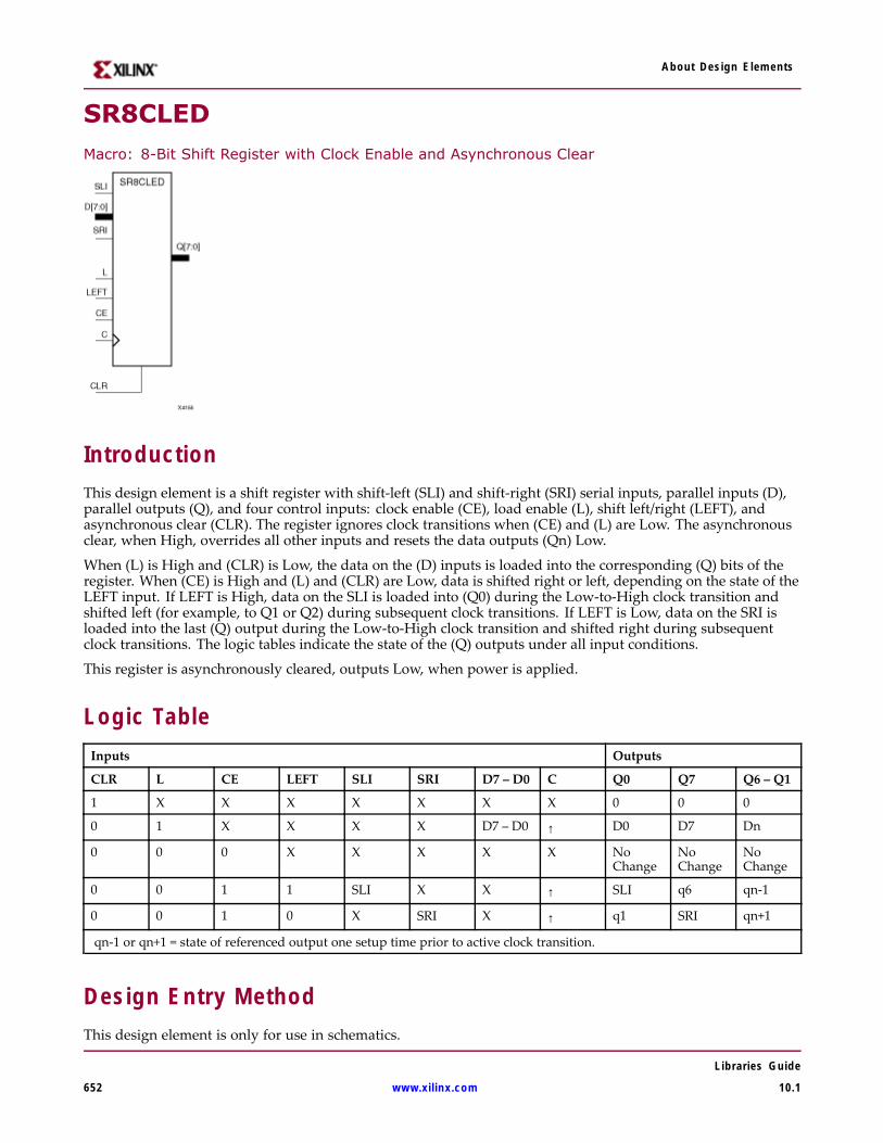
About Design Elements
SR8CLEDMacro: 8-Bit Shift Register with Clock Enable and Asynchronous Clear
IntroductionThis design element is a shift register with shift-left (SLI) and shift-right (SRI) serial inputs, parallel inputs (D),parallel outputs (Q), and four control inputs: clock enable (CE), load enable (L), shift left/right (LEFT), andasynchronous clear (CLR). The register ignores clock transitions when (CE) and (L) are Low. The asynchronousclear, when High, overrides all other inputs and resets the data outputs (Qn) Low.
When (L) is High and (CLR) is Low, the data on the (D) inputs is loaded into the corresponding (Q) bits of theregister. When (CE) is High and (L) and (CLR) are Low, data is shifted right or left, depending on the state of theLEFT input. If LEFT is High, data on the SLI is loaded into (Q0) during the Low-to-High clock transition andshifted left (for example, to Q1 or Q2) during subsequent clock transitions. If LEFT is Low, data on the SRI isloaded into the last (Q) output during the Low-to-High clock transition and shifted right during subsequentclock transitions. The logic tables indicate the state of the (Q) outputs under all input conditions.
This register is asynchronously cleared, outputs Low, when power is applied.
Logic TableInputs Outputs
CLR L CE LEFT SLI SRI D7 – D0 C Q0 Q7 Q6 – Q1
1 X X X X X X X 0 0 0
0 1 X X X X D7 – D0 ↑ D0 D7 Dn
0 0 0 X X X X X NoChange
NoChange
NoChange
0 0 1 1 SLI X X ↑ SLI q6 qn-1
0 0 1 0 X SRI X ↑ q1 SRI qn+1
qn-1 or qn+1 = state of referenced output one setup time prior to active clock transition.
Design Entry MethodThis design element is only for use in schematics.
Libraries Guide
652 www.xilinx.com 10.1

About Design Elements
For More Information• See the Virtex-4 User Guide.
• See the Virtex-4 Data Sheets.
Libraries Guide
10.1 www.xilinx.com 653
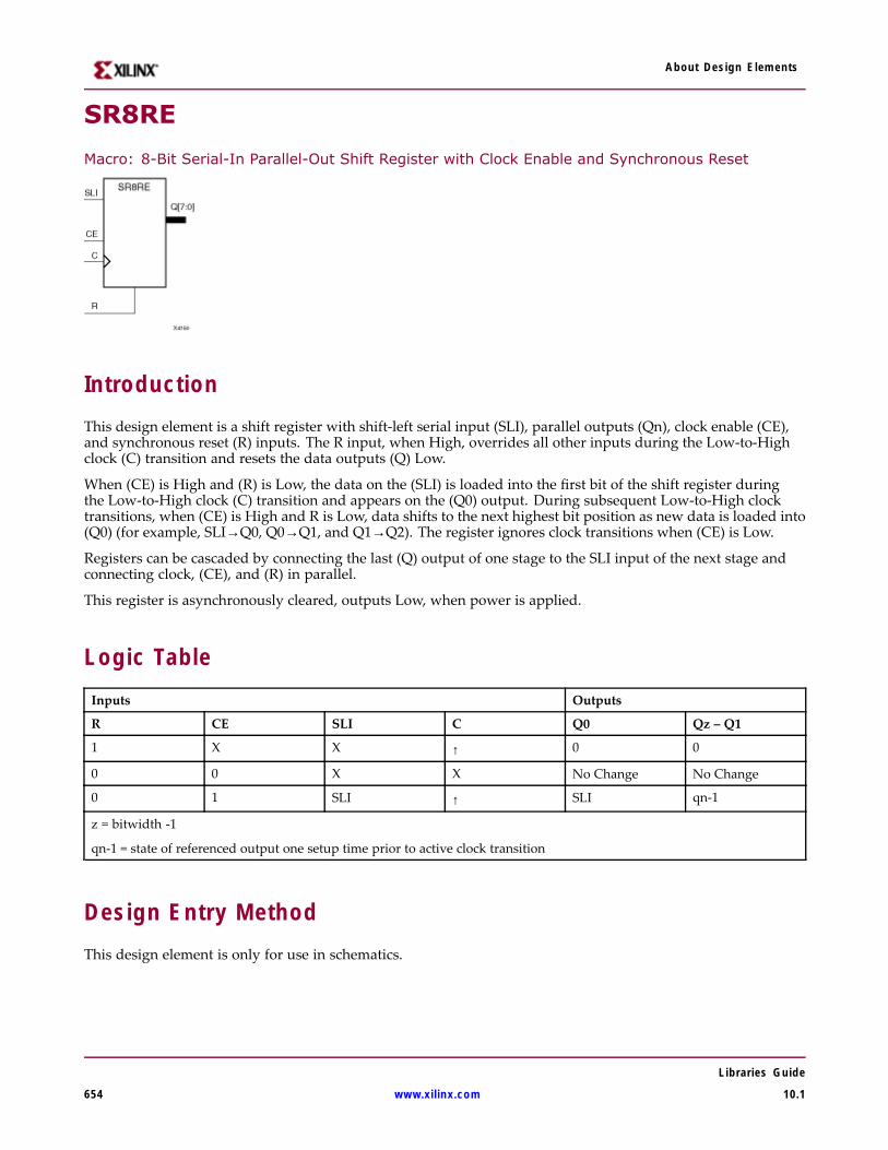
About Design Elements
SR8RE
Macro: 8-Bit Serial-In Parallel-Out Shift Register with Clock Enable and Synchronous Reset
IntroductionThis design element is a shift register with shift-left serial input (SLI), parallel outputs (Qn), clock enable (CE),and synchronous reset (R) inputs. The R input, when High, overrides all other inputs during the Low-to-Highclock (C) transition and resets the data outputs (Q) Low.
When (CE) is High and (R) is Low, the data on the (SLI) is loaded into the first bit of the shift register duringthe Low-to-High clock (C) transition and appears on the (Q0) output. During subsequent Low-to-High clocktransitions, when (CE) is High and R is Low, data shifts to the next highest bit position as new data is loaded into(Q0) (for example, SLI→Q0, Q0→Q1, and Q1→Q2). The register ignores clock transitions when (CE) is Low.
Registers can be cascaded by connecting the last (Q) output of one stage to the SLI input of the next stage andconnecting clock, (CE), and (R) in parallel.
This register is asynchronously cleared, outputs Low, when power is applied.
Logic TableInputs Outputs
R CE SLI C Q0 Qz – Q1
1 X X ↑ 0 0
0 0 X X No Change No Change
0 1 SLI ↑ SLI qn-1
z = bitwidth -1
qn-1 = state of referenced output one setup time prior to active clock transition
Design Entry MethodThis design element is only for use in schematics.
Libraries Guide
654 www.xilinx.com 10.1

About Design Elements
For More Information• See the Virtex-4 User Guide.
• See the Virtex-4 Data Sheets.
Libraries Guide
10.1 www.xilinx.com 655
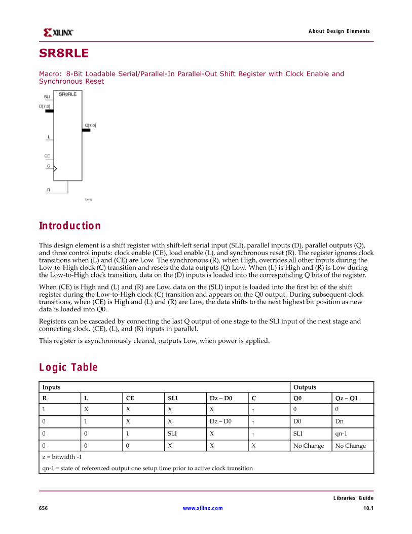
About Design Elements
SR8RLE
Macro: 8-Bit Loadable Serial/Parallel-In Parallel-Out Shift Register with Clock Enable andSynchronous Reset
IntroductionThis design element is a shift register with shift-left serial input (SLI), parallel inputs (D), parallel outputs (Q),and three control inputs: clock enable (CE), load enable (L), and synchronous reset (R). The register ignores clocktransitions when (L) and (CE) are Low. The synchronous (R), when High, overrides all other inputs during theLow-to-High clock (C) transition and resets the data outputs (Q) Low. When (L) is High and (R) is Low duringthe Low-to-High clock transition, data on the (D) inputs is loaded into the corresponding Q bits of the register.
When (CE) is High and (L) and (R) are Low, data on the (SLI) input is loaded into the first bit of the shiftregister during the Low-to-High clock (C) transition and appears on the Q0 output. During subsequent clocktransitions, when (CE) is High and (L) and (R) are Low, the data shifts to the next highest bit position as newdata is loaded into Q0.
Registers can be cascaded by connecting the last Q output of one stage to the SLI input of the next stage andconnecting clock, (CE), (L), and (R) inputs in parallel.
This register is asynchronously cleared, outputs Low, when power is applied.
Logic TableInputs Outputs
R L CE SLI Dz – D0 C Q0 Qz – Q1
1 X X X X ↑ 0 0
0 1 X X Dz – D0 ↑ D0 Dn
0 0 1 SLI X ↑ SLI qn-1
0 0 0 X X X No Change No Change
z = bitwidth -1
qn-1 = state of referenced output one setup time prior to active clock transition
Libraries Guide
656 www.xilinx.com 10.1

About Design Elements
Design Entry MethodThis design element is only for use in schematics.
For More Information• See the Virtex-4 User Guide.
• See the Virtex-4 Data Sheets.
Libraries Guide
10.1 www.xilinx.com 657

About Design Elements
SR8RLED
Macro: 8-Bit Shift Register with Clock Enable and Synchronous Reset
IntroductionThis design element is a shift register with shift-left (SLI) and shift-right (SRI) serial inputs, parallel inputs (D),parallel outputs (Q) and four control inputs — clock enable (CE), load enable (L), shift left/right (LEFT), andsynchronous reset (R). The register ignores clock transitions when (CE) and (L) are Low. The synchronous (R),when High, overrides all other inputs during the Low-to-High clock (C) transition and resets the data outputs(Q) Low. When (L) is High and (R) is Low during the Low-to-High clock transition, the data on the (D) inputs isloaded into the corresponding (Q) bits of the register.
When (CE) is High and (L) and (R) are Low, data shifts right or left, depending on the state of the LEFT input.If LEFT is High, data on (SLI) is loaded into (Q0) during the Low-to-High clock transition and shifted left (forexample, to Q1 and Q2) during subsequent clock transitions. If LEFT is Low, data on the (SRI) is loaded into thelast (Q) output during the Low-to-High clock transition and shifted right ) during subsequent clock transitions.The logic tables below indicates the state of the (Q) outputs under all input conditions.
This register is asynchronously cleared, outputs Low, when power is applied.
Logic TableInputs Outputs
R L CE LEFT SLI SRI D7– D0 C Q0 Q7 Q6 – Q1
1 X X X X X X ↑ 0 0 0
0 1 X X X X D7 – D0 ↑ D0 D7 Dn
0 0 0 X X X X X NoChange
NoChange
NoChange
0 0 1 1 SLI X X ↑ SLI q6 qn-1
0 0 1 0 X SRI X ↑ q1 SRI qn+1
qn-1 or qn+1 = state of referenced output one setup time prior to active clock transition
Libraries Guide
658 www.xilinx.com 10.1

About Design Elements
Design Entry MethodThis design element is only for use in schematics.
For More Information• See the Virtex-4 User Guide.
• See the Virtex-4 Data Sheets.
Libraries Guide
10.1 www.xilinx.com 659

About Design Elements
SRL16
Primitive: 16-Bit Shift Register Look-Up-Table (LUT)
IntroductionThis design element is a shift register look-up table (LUT). The inputs A3, A2, A1, and A0 select the outputlength of the shift register.
The shift register can be of a fixed, static length or it can be dynamically adjusted.
• To create a fixed-length shift register - Drive the A3 through A0 inputs with static values. The length ofthe shift register can vary from 1 bit to 16 bits, as determined by the following formula: Length = (8 x A3)+(4 x A2) + (2 x A1) + A0 +1 If A3, A2, A1, and A0 are all zeros (0000), the shift register is one bit long. Ifthey are all ones (1111), it is 16 bits long.
• To change the length of the shift register dynamically - Change the values driving the A3 through A0inputs. For example, if A2, A1, and A0 are all ones (111) and A3 toggles between a one (1) and a zero (0), thelength of the shift register changes from 16 bits to 8 bits. Internally, the length of the shift register is always 16bits and the input lines A3 through A0 select which of the 16 bits reach the output.
The shift register LUT contents are initialized by assigning a four-digit hexadecimal number to an INIT attribute.The first, or the left-most, hexadecimal digit is the most significant bit. If an INIT value is not specified, it defaultsto a value of four zeros (0000) so that the shift register LUT is cleared during configuration.
The data (D) is loaded into the first bit of the shift register during the Low-to-High clock (CLK) transition. Duringsubsequent Low-to-High clock transitions data shifts to the next highest bit position while new data is loaded.The data appears on the Q output when the shift register length determined by the address inputs is reached.
Logic TableInputs Output
Am CLK D Q
Am X X Q(Am)
Am ↑ D Q(Am - 1)
m= 0, 1, 2, 3
Design Entry MethodThis design element can be used in schematics.
Libraries Guide
660 www.xilinx.com 10.1
About Design Elements
Available AttributesAttribute Type Allowed Values Default Description
INIT Hexadecimal Any 16-Bit Value All zeros Sets the initial value of Q output afterconfiguration.
For More Information• See the Virtex-4 User Guide.
• See the Virtex-4 Data Sheets.
Libraries Guide
10.1 www.xilinx.com 661
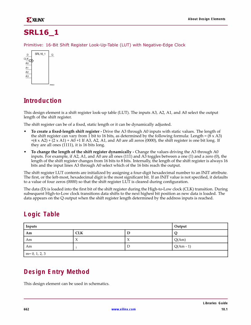
About Design Elements
SRL16_1
Primitive: 16-Bit Shift Register Look-Up-Table (LUT) with Negative-Edge Clock
IntroductionThis design element is a shift register look-up table (LUT). The inputs A3, A2, A1, and A0 select the outputlength of the shift register.
The shift register can be of a fixed, static length or it can be dynamically adjusted.
• To create a fixed-length shift register - Drive the A3 through A0 inputs with static values. The length ofthe shift register can vary from 1 bit to 16 bits, as determined by the following formula: Length = (8 x A3)+(4 x A2) + (2 x A1) + A0 +1 If A3, A2, A1, and A0 are all zeros (0000), the shift register is one bit long. Ifthey are all ones (1111), it is 16 bits long.
• To change the length of the shift register dynamically - Change the values driving the A3 through A0inputs. For example, if A2, A1, and A0 are all ones (111) and A3 toggles between a one (1) and a zero (0), thelength of the shift register changes from 16 bits to 8 bits. Internally, the length of the shift register is always 16bits and the input lines A3 through A0 select which of the 16 bits reach the output.
The shift register LUT contents are initialized by assigning a four-digit hexadecimal number to an INIT attribute.The first, or the left-most, hexadecimal digit is the most significant bit. If an INIT value is not specified, it defaultsto a value of four zeros (0000) so that the shift register LUT is cleared during configuration.
The data (D) is loaded into the first bit of the shift register during the High-to-Low clock (CLK) transition. Duringsubsequent High-to-Low clock transitions data shifts to the next highest bit position as new data is loaded. Thedata appears on the Q output when the shift register length determined by the address inputs is reached.
Logic TableInputs Output
Am CLK D Q
Am X X Q(Am)
Am ↓ D Q(Am - 1)
m= 0, 1, 2, 3
Design Entry MethodThis design element can be used in schematics.
Libraries Guide
662 www.xilinx.com 10.1
About Design Elements
Available AttributesAttribute Type Allowed Values Default Description
INIT Hexadecimal Any 16-Bit Value All zeros Sets the initial value of Q output afterconfiguration
For More Information• See the Virtex-4 User Guide.
• See the Virtex-4 Data Sheets.
Libraries Guide
10.1 www.xilinx.com 663
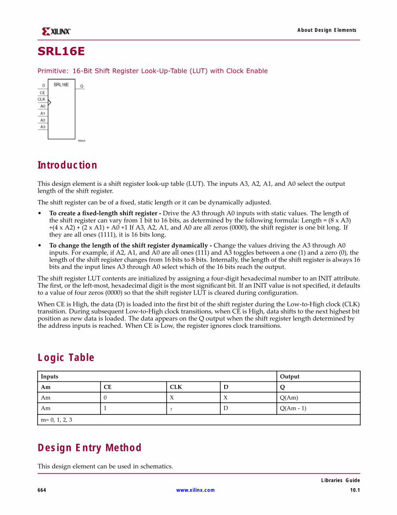
About Design Elements
SRL16E
Primitive: 16-Bit Shift Register Look-Up-Table (LUT) with Clock Enable
IntroductionThis design element is a shift register look-up table (LUT). The inputs A3, A2, A1, and A0 select the outputlength of the shift register.
The shift register can be of a fixed, static length or it can be dynamically adjusted.• To create a fixed-length shift register - Drive the A3 through A0 inputs with static values. The length of
the shift register can vary from 1 bit to 16 bits, as determined by the following formula: Length = (8 x A3)+(4 x A2) + (2 x A1) + A0 +1 If A3, A2, A1, and A0 are all zeros (0000), the shift register is one bit long. Ifthey are all ones (1111), it is 16 bits long.
• To change the length of the shift register dynamically - Change the values driving the A3 through A0inputs. For example, if A2, A1, and A0 are all ones (111) and A3 toggles between a one (1) and a zero (0), thelength of the shift register changes from 16 bits to 8 bits. Internally, the length of the shift register is always 16bits and the input lines A3 through A0 select which of the 16 bits reach the output.
The shift register LUT contents are initialized by assigning a four-digit hexadecimal number to an INIT attribute.The first, or the left-most, hexadecimal digit is the most significant bit. If an INIT value is not specified, it defaultsto a value of four zeros (0000) so that the shift register LUT is cleared during configuration.
When CE is High, the data (D) is loaded into the first bit of the shift register during the Low-to-High clock (CLK)transition. During subsequent Low-to-High clock transitions, when CE is High, data shifts to the next highest bitposition as new data is loaded. The data appears on the Q output when the shift register length determined bythe address inputs is reached. When CE is Low, the register ignores clock transitions.
Logic TableInputs Output
Am CE CLK D Q
Am 0 X X Q(Am)
Am 1 ↑ D Q(Am - 1)
m= 0, 1, 2, 3
Design Entry MethodThis design element can be used in schematics.
Libraries Guide
664 www.xilinx.com 10.1
About Design Elements
Available AttributesAttribute Type Allowed Values Default Description
INIT Hexadecimal Any 16-Bit Value All zeros Sets the initial value of content and output of shiftregister after configuration.
For More Information• See the Virtex-4 User Guide.
• See the Virtex-4 Data Sheets.
Libraries Guide
10.1 www.xilinx.com 665
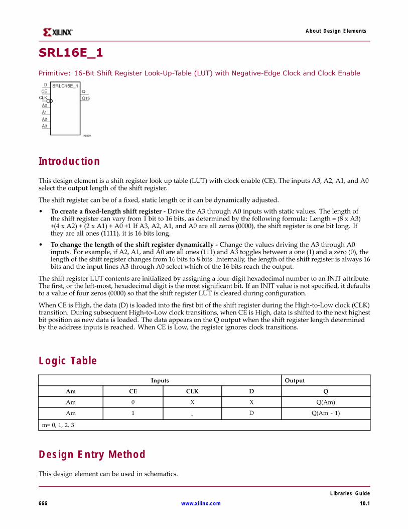
About Design Elements
SRL16E_1
Primitive: 16-Bit Shift Register Look-Up-Table (LUT) with Negative-Edge Clock and Clock Enable
IntroductionThis design element is a shift register look up table (LUT) with clock enable (CE). The inputs A3, A2, A1, and A0select the output length of the shift register.
The shift register can be of a fixed, static length or it can be dynamically adjusted.
• To create a fixed-length shift register - Drive the A3 through A0 inputs with static values. The length ofthe shift register can vary from 1 bit to 16 bits, as determined by the following formula: Length = (8 x A3)+(4 x A2) + (2 x A1) + A0 +1 If A3, A2, A1, and A0 are all zeros (0000), the shift register is one bit long. Ifthey are all ones (1111), it is 16 bits long.
• To change the length of the shift register dynamically - Change the values driving the A3 through A0inputs. For example, if A2, A1, and A0 are all ones (111) and A3 toggles between a one (1) and a zero (0), thelength of the shift register changes from 16 bits to 8 bits. Internally, the length of the shift register is always 16bits and the input lines A3 through A0 select which of the 16 bits reach the output.
The shift register LUT contents are initialized by assigning a four-digit hexadecimal number to an INIT attribute.The first, or the left-most, hexadecimal digit is the most significant bit. If an INIT value is not specified, it defaultsto a value of four zeros (0000) so that the shift register LUT is cleared during configuration.
When CE is High, the data (D) is loaded into the first bit of the shift register during the High-to-Low clock (CLK)transition. During subsequent High-to-Low clock transitions, when CE is High, data is shifted to the next highestbit position as new data is loaded. The data appears on the Q output when the shift register length determinedby the address inputs is reached. When CE is Low, the register ignores clock transitions.
Logic TableInputs Output
Am CE CLK D Q
Am 0 X X Q(Am)
Am 1 ↓ D Q(Am - 1)
m= 0, 1, 2, 3
Design Entry MethodThis design element can be used in schematics.
Libraries Guide
666 www.xilinx.com 10.1

About Design Elements
Available Attributes
Attribute TypeAllowedValues Default Description
INIT Hexadecimal Any 16-BitValue
All zeros Sets the initial value of content and output of shiftregister after configuration.
For More Information• See the Virtex-4 User Guide.
• See the Virtex-4 Data Sheets.
Libraries Guide
10.1 www.xilinx.com 667
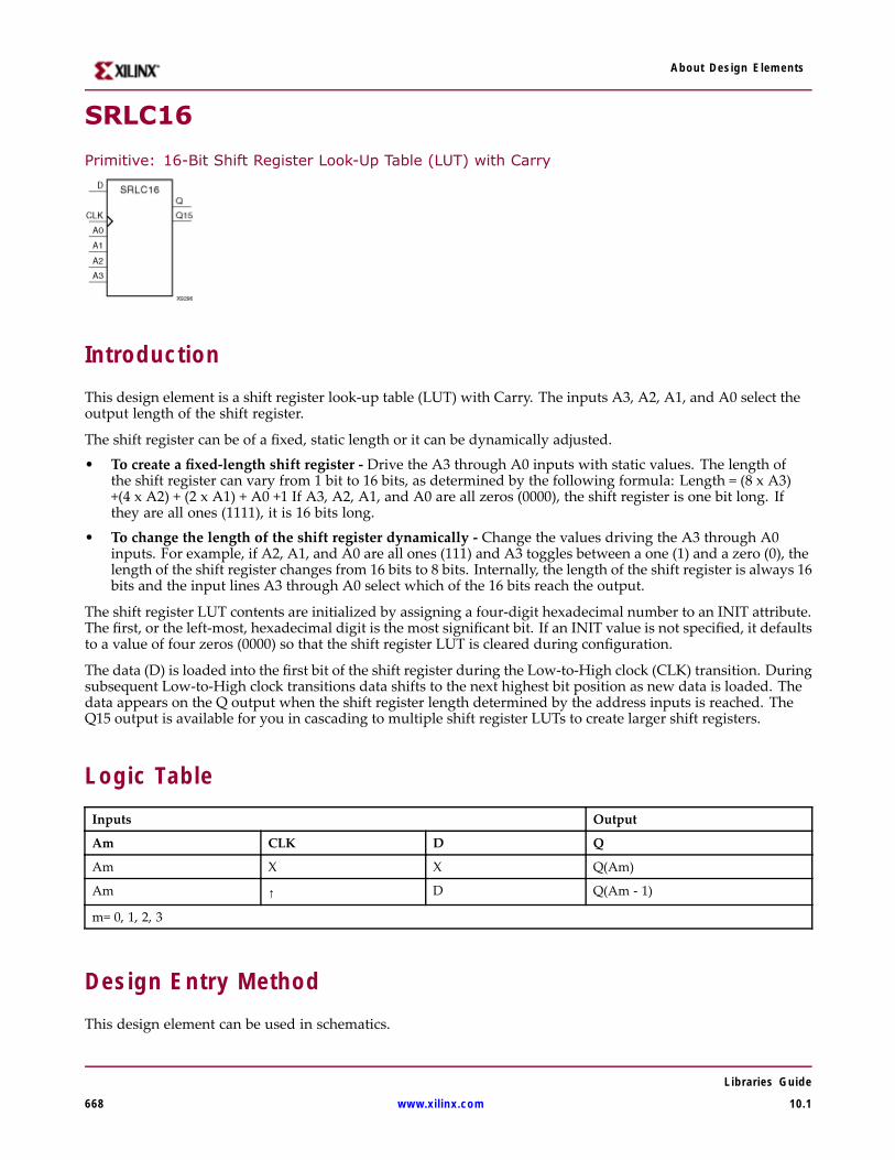
About Design Elements
SRLC16
Primitive: 16-Bit Shift Register Look-Up Table (LUT) with Carry
IntroductionThis design element is a shift register look-up table (LUT) with Carry. The inputs A3, A2, A1, and A0 select theoutput length of the shift register.
The shift register can be of a fixed, static length or it can be dynamically adjusted.
• To create a fixed-length shift register - Drive the A3 through A0 inputs with static values. The length ofthe shift register can vary from 1 bit to 16 bits, as determined by the following formula: Length = (8 x A3)+(4 x A2) + (2 x A1) + A0 +1 If A3, A2, A1, and A0 are all zeros (0000), the shift register is one bit long. Ifthey are all ones (1111), it is 16 bits long.
• To change the length of the shift register dynamically - Change the values driving the A3 through A0inputs. For example, if A2, A1, and A0 are all ones (111) and A3 toggles between a one (1) and a zero (0), thelength of the shift register changes from 16 bits to 8 bits. Internally, the length of the shift register is always 16bits and the input lines A3 through A0 select which of the 16 bits reach the output.
The shift register LUT contents are initialized by assigning a four-digit hexadecimal number to an INIT attribute.The first, or the left-most, hexadecimal digit is the most significant bit. If an INIT value is not specified, it defaultsto a value of four zeros (0000) so that the shift register LUT is cleared during configuration.
The data (D) is loaded into the first bit of the shift register during the Low-to-High clock (CLK) transition. Duringsubsequent Low-to-High clock transitions data shifts to the next highest bit position as new data is loaded. Thedata appears on the Q output when the shift register length determined by the address inputs is reached. TheQ15 output is available for you in cascading to multiple shift register LUTs to create larger shift registers.
Logic TableInputs Output
Am CLK D Q
Am X X Q(Am)
Am ↑ D Q(Am - 1)
m= 0, 1, 2, 3
Design Entry MethodThis design element can be used in schematics.
Libraries Guide
668 www.xilinx.com 10.1
About Design Elements
Available AttributesAttribute Type Allowed Values Default Description
INIT Hexadecimal Any 16-Bit Value All zeros Sets the initial value of content and output of shiftregister after configuration.
For More Information• See the Virtex-4 User Guide.
• See the Virtex-4 Data Sheets.
Libraries Guide
10.1 www.xilinx.com 669

About Design Elements
SRLC16_1Primitive: 16-Bit Shift Register Look-Up Table (LUT) with Carry and Negative-Edge Clock
IntroductionThis design element is a shift register look-up table (LUT) with carry and a negative-edge clock. The inputs A3,A2, A1, and A0 select the output length of the shift register.
The shift register can be of a fixed, static length or it can be dynamically adjusted.• To create a fixed-length shift register - Drive the A3 through A0 inputs with static values. The length of
the shift register can vary from 1 bit to 16 bits, as determined by the following formula: Length = (8 x A3)+(4 x A2) + (2 x A1) + A0 +1 If A3, A2, A1, and A0 are all zeros (0000), the shift register is one bit long. Ifthey are all ones (1111), it is 16 bits long.
• To change the length of the shift register dynamically - Change the values driving the A3 through A0inputs. For example, if A2, A1, and A0 are all ones (111) and A3 toggles between a one (1) and a zero (0), thelength of the shift register changes from 16 bits to 8 bits. Internally, the length of the shift register is always 16bits and the input lines A3 through A0 select which of the 16 bits reach the output.
The shift register LUT contents are initialized by assigning a four-digit hexadecimal number to an INIT attribute.The first, or the left-most, hexadecimal digit is the most significant bit. If an INIT value is not specified, it defaultsto a value of four zeros (0000) so that the shift register LUT is cleared during configuration.
The Q15 output is available for your use in cascading multiple shift register LUTs to create larger shift registers.
Logic TableInputs Output
Am CLK D Q Q15
Am X X Q(Am) No Change
Am ↓ D Q(Am - 1) Q14
m= 0, 1, 2, 3
Design Entry MethodThis design element can be used in schematics.
Available AttributesAttribute Type Allowed Values Default Description
INIT Hexadecimal Any 16-Bit Value All zeros Sets the initial value of content and output of shiftregister after configuration.
Libraries Guide
670 www.xilinx.com 10.1

About Design Elements
For More Information• See the Virtex-4 User Guide.
• See the Virtex-4 Data Sheets.
Libraries Guide
10.1 www.xilinx.com 671
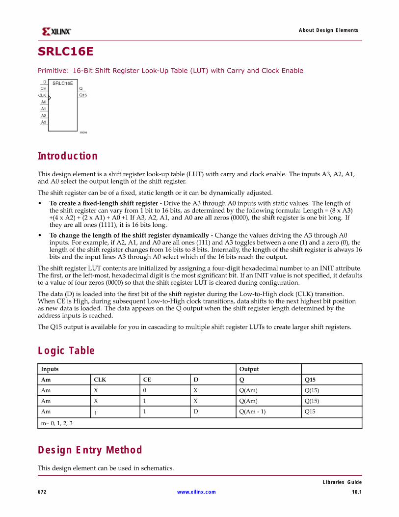
About Design Elements
SRLC16E
Primitive: 16-Bit Shift Register Look-Up Table (LUT) with Carry and Clock Enable
IntroductionThis design element is a shift register look-up table (LUT) with carry and clock enable. The inputs A3, A2, A1,and A0 select the output length of the shift register.
The shift register can be of a fixed, static length or it can be dynamically adjusted.• To create a fixed-length shift register - Drive the A3 through A0 inputs with static values. The length of
the shift register can vary from 1 bit to 16 bits, as determined by the following formula: Length = (8 x A3)+(4 x A2) + (2 x A1) + A0 +1 If A3, A2, A1, and A0 are all zeros (0000), the shift register is one bit long. Ifthey are all ones (1111), it is 16 bits long.
• To change the length of the shift register dynamically - Change the values driving the A3 through A0inputs. For example, if A2, A1, and A0 are all ones (111) and A3 toggles between a one (1) and a zero (0), thelength of the shift register changes from 16 bits to 8 bits. Internally, the length of the shift register is always 16bits and the input lines A3 through A0 select which of the 16 bits reach the output.
The shift register LUT contents are initialized by assigning a four-digit hexadecimal number to an INIT attribute.The first, or the left-most, hexadecimal digit is the most significant bit. If an INIT value is not specified, it defaultsto a value of four zeros (0000) so that the shift register LUT is cleared during configuration.
The data (D) is loaded into the first bit of the shift register during the Low-to-High clock (CLK) transition.When CE is High, during subsequent Low-to-High clock transitions, data shifts to the next highest bit positionas new data is loaded. The data appears on the Q output when the shift register length determined by theaddress inputs is reached.
The Q15 output is available for you in cascading to multiple shift register LUTs to create larger shift registers.
Logic TableInputs Output
Am CLK CE D Q Q15
Am X 0 X Q(Am) Q(15)
Am X 1 X Q(Am) Q(15)
Am ↑ 1 D Q(Am - 1) Q15
m= 0, 1, 2, 3
Design Entry MethodThis design element can be used in schematics.
Libraries Guide
672 www.xilinx.com 10.1

About Design Elements
Available AttributesAttribute Type Allowed Values Default Description
INIT Hexadecimal Any 16-Bit Value All zeros Sets the initial value of content and output of shiftregister after configuration.
For More Information• See the Virtex-4 User Guide.
• See the Virtex-4 Data Sheets.
Libraries Guide
10.1 www.xilinx.com 673
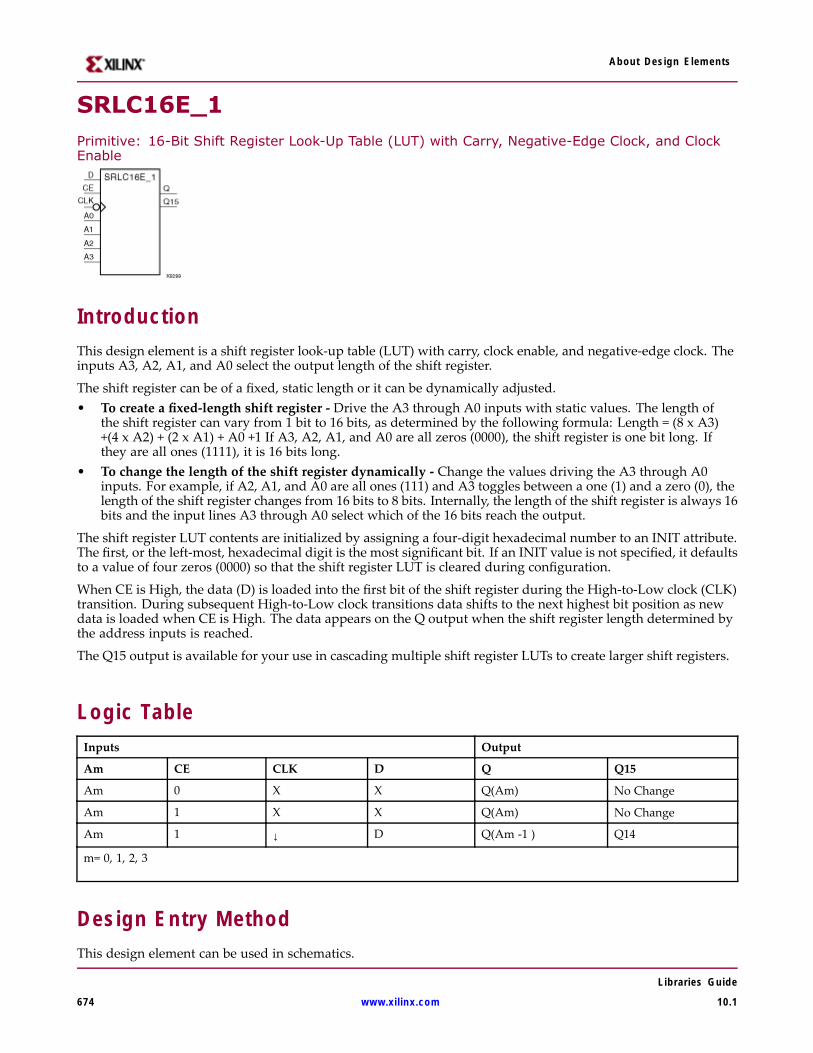
About Design Elements
SRLC16E_1Primitive: 16-Bit Shift Register Look-Up Table (LUT) with Carry, Negative-Edge Clock, and ClockEnable
IntroductionThis design element is a shift register look-up table (LUT) with carry, clock enable, and negative-edge clock. Theinputs A3, A2, A1, and A0 select the output length of the shift register.
The shift register can be of a fixed, static length or it can be dynamically adjusted.• To create a fixed-length shift register - Drive the A3 through A0 inputs with static values. The length of
the shift register can vary from 1 bit to 16 bits, as determined by the following formula: Length = (8 x A3)+(4 x A2) + (2 x A1) + A0 +1 If A3, A2, A1, and A0 are all zeros (0000), the shift register is one bit long. Ifthey are all ones (1111), it is 16 bits long.
• To change the length of the shift register dynamically - Change the values driving the A3 through A0inputs. For example, if A2, A1, and A0 are all ones (111) and A3 toggles between a one (1) and a zero (0), thelength of the shift register changes from 16 bits to 8 bits. Internally, the length of the shift register is always 16bits and the input lines A3 through A0 select which of the 16 bits reach the output.
The shift register LUT contents are initialized by assigning a four-digit hexadecimal number to an INIT attribute.The first, or the left-most, hexadecimal digit is the most significant bit. If an INIT value is not specified, it defaultsto a value of four zeros (0000) so that the shift register LUT is cleared during configuration.
When CE is High, the data (D) is loaded into the first bit of the shift register during the High-to-Low clock (CLK)transition. During subsequent High-to-Low clock transitions data shifts to the next highest bit position as newdata is loaded when CE is High. The data appears on the Q output when the shift register length determined bythe address inputs is reached.
The Q15 output is available for your use in cascading multiple shift register LUTs to create larger shift registers.
Logic TableInputs Output
Am CE CLK D Q Q15
Am 0 X X Q(Am) No Change
Am 1 X X Q(Am) No Change
Am 1 ↓ D Q(Am -1 ) Q14
m= 0, 1, 2, 3
Design Entry MethodThis design element can be used in schematics.
Libraries Guide
674 www.xilinx.com 10.1

About Design Elements
Available Attributes
Attribute TypeAllowedValues Default Description
INIT Hexadecimal Any 16-BitValue
All zeros Sets the initial value of content and output of shift registerafter configuration.
For More Information• See the Virtex-4 User Guide.
• See the Virtex-4 Data Sheets.
Libraries Guide
10.1 www.xilinx.com 675
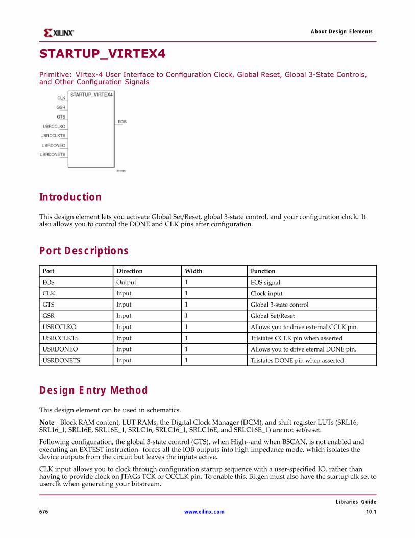
About Design Elements
STARTUP_VIRTEX4
Primitive: Virtex-4 User Interface to Configuration Clock, Global Reset, Global 3-State Controls,and Other Configuration Signals
IntroductionThis design element lets you activate Global Set/Reset, global 3-state control, and your configuration clock. Italso allows you to control the DONE and CLK pins after configuration.
Port DescriptionsPort Direction Width Function
EOS Output 1 EOS signal
CLK Input 1 Clock input
GTS Input 1 Global 3-state control
GSR Input 1 Global Set/Reset
USRCCLKO Input 1 Allows you to drive external CCLK pin.
USRCCLKTS Input 1 Tristates CCLK pin when asserted
USRDONEO Input 1 Allows you to drive eternal DONE pin.
USRDONETS Input 1 Tristates DONE pin when asserted.
Design Entry MethodThis design element can be used in schematics.
Note Block RAM content, LUT RAMs, the Digital Clock Manager (DCM), and shift register LUTs (SRL16,SRL16_1, SRL16E, SRL16E_1, SRLC16, SRLC16_1, SRLC16E, and SRLC16E_1) are not set/reset.
Following configuration, the global 3-state control (GTS), when High--and when BSCAN, is not enabled andexecuting an EXTEST instruction--forces all the IOB outputs into high-impedance mode, which isolates thedevice outputs from the circuit but leaves the inputs active.
CLK input allows you to clock through configuration startup sequence with a user-specified IO, rather thanhaving to provide clock on JTAGs TCK or CCCLK pin. To enable this, Bitgen must also have the startup clk set touserclk when generating your bitstream.
Libraries Guide
676 www.xilinx.com 10.1

About Design Elements
USRCLKO/TS and USRDONEO/TS are used to control the external DONE and CCLK pins. Using theSTARTUP_VIRTEX4 in combination with the USR_ACCESS_VIRTEX4 primitive supports a variety ofapplications, such as loading PROM data into the FPGA for various uses. Refer to USR_ACCESS_VIRTEX4 formore information.
For More Information• See the Virtex-4 User Guide.
• See the Virtex-4 Data Sheets.
Libraries Guide
10.1 www.xilinx.com 677
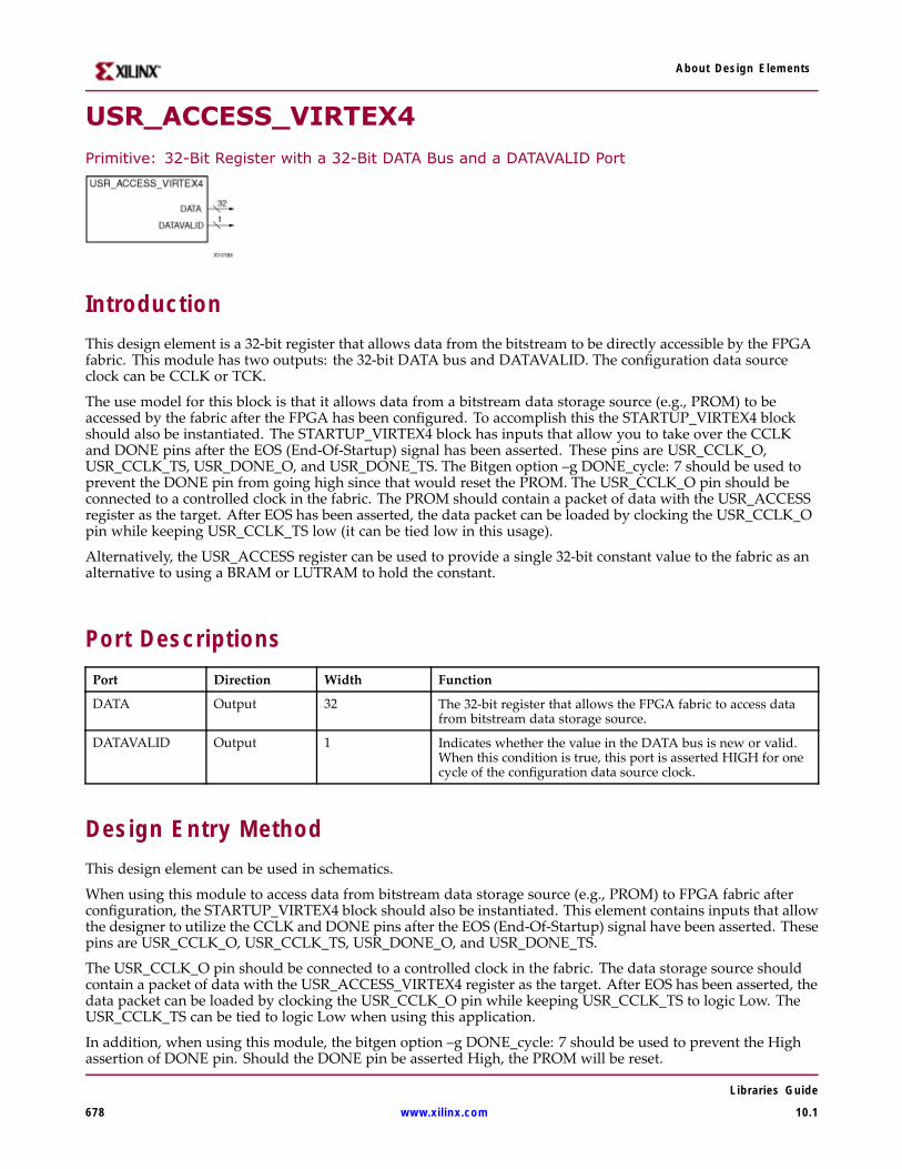
About Design Elements
USR_ACCESS_VIRTEX4Primitive: 32-Bit Register with a 32-Bit DATA Bus and a DATAVALID Port
IntroductionThis design element is a 32-bit register that allows data from the bitstream to be directly accessible by the FPGAfabric. This module has two outputs: the 32-bit DATA bus and DATAVALID. The configuration data sourceclock can be CCLK or TCK.
The use model for this block is that it allows data from a bitstream data storage source (e.g., PROM) to beaccessed by the fabric after the FPGA has been configured. To accomplish this the STARTUP_VIRTEX4 blockshould also be instantiated. The STARTUP_VIRTEX4 block has inputs that allow you to take over the CCLKand DONE pins after the EOS (End-Of-Startup) signal has been asserted. These pins are USR_CCLK_O,USR_CCLK_TS, USR_DONE_O, and USR_DONE_TS. The Bitgen option –g DONE_cycle: 7 should be used toprevent the DONE pin from going high since that would reset the PROM. The USR_CCLK_O pin should beconnected to a controlled clock in the fabric. The PROM should contain a packet of data with the USR_ACCESSregister as the target. After EOS has been asserted, the data packet can be loaded by clocking the USR_CCLK_Opin while keeping USR_CCLK_TS low (it can be tied low in this usage).
Alternatively, the USR_ACCESS register can be used to provide a single 32-bit constant value to the fabric as analternative to using a BRAM or LUTRAM to hold the constant.
Port DescriptionsPort Direction Width Function
DATA Output 32 The 32-bit register that allows the FPGA fabric to access datafrom bitstream data storage source.
DATAVALID Output 1 Indicates whether the value in the DATA bus is new or valid.When this condition is true, this port is asserted HIGH for onecycle of the configuration data source clock.
Design Entry MethodThis design element can be used in schematics.
When using this module to access data from bitstream data storage source (e.g., PROM) to FPGA fabric afterconfiguration, the STARTUP_VIRTEX4 block should also be instantiated. This element contains inputs that allowthe designer to utilize the CCLK and DONE pins after the EOS (End-Of-Startup) signal have been asserted. Thesepins are USR_CCLK_O, USR_CCLK_TS, USR_DONE_O, and USR_DONE_TS.
The USR_CCLK_O pin should be connected to a controlled clock in the fabric. The data storage source shouldcontain a packet of data with the USR_ACCESS_VIRTEX4 register as the target. After EOS has been asserted, thedata packet can be loaded by clocking the USR_CCLK_O pin while keeping USR_CCLK_TS to logic Low. TheUSR_CCLK_TS can be tied to logic Low when using this application.
In addition, when using this module, the bitgen option –g DONE_cycle: 7 should be used to prevent the Highassertion of DONE pin. Should the DONE pin be asserted High, the PROM will be reset.
Libraries Guide
678 www.xilinx.com 10.1

About Design Elements
For More Information• See the Virtex-4 User Guide.
• See the Virtex-4 Data Sheets.
Libraries Guide
10.1 www.xilinx.com 679
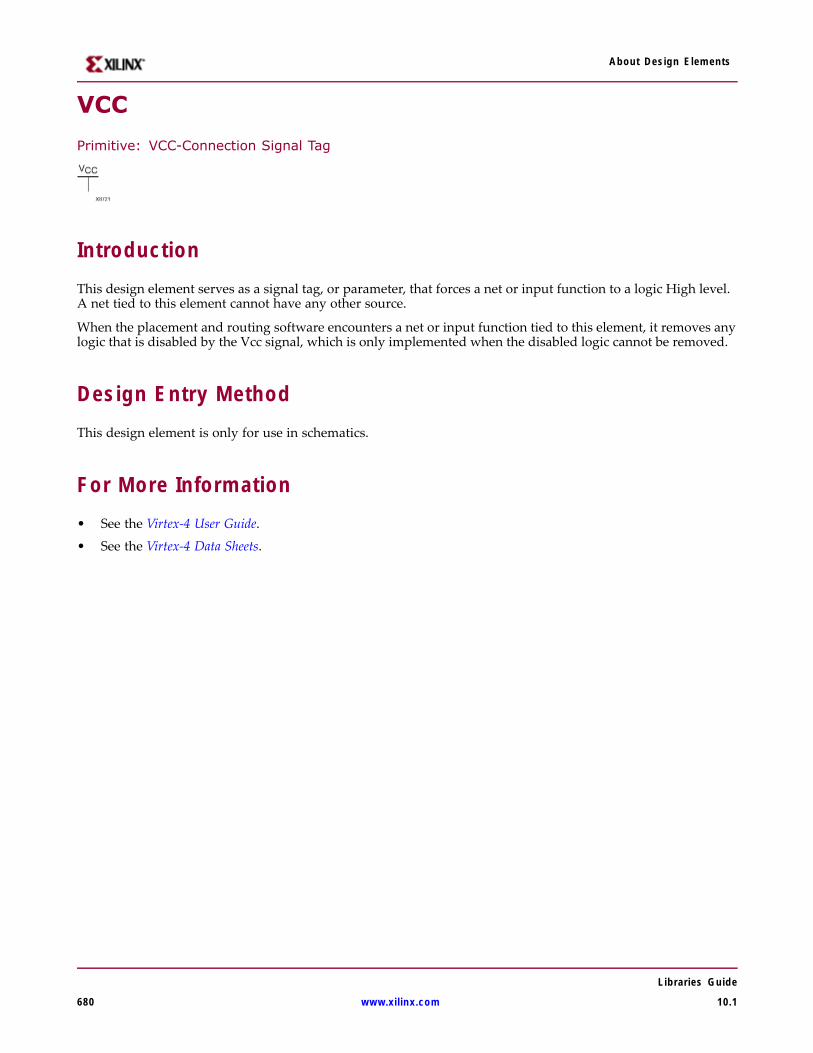
About Design Elements
VCC
Primitive: VCC-Connection Signal Tag
IntroductionThis design element serves as a signal tag, or parameter, that forces a net or input function to a logic High level.A net tied to this element cannot have any other source.
When the placement and routing software encounters a net or input function tied to this element, it removes anylogic that is disabled by the Vcc signal, which is only implemented when the disabled logic cannot be removed.
Design Entry MethodThis design element is only for use in schematics.
For More Information• See the Virtex-4 User Guide.
• See the Virtex-4 Data Sheets.
Libraries Guide
680 www.xilinx.com 10.1
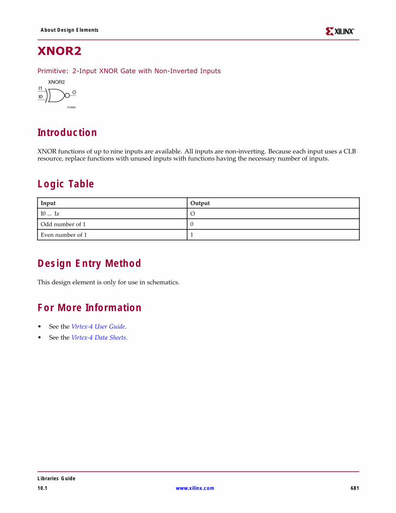
About Design Elements
XNOR2
Primitive: 2-Input XNOR Gate with Non-Inverted Inputs
IntroductionXNOR functions of up to nine inputs are available. All inputs are non-inverting. Because each input uses a CLBresource, replace functions with unused inputs with functions having the necessary number of inputs.
Logic TableInput Output
I0 ... Iz O
Odd number of 1 0
Even number of 1 1
Design Entry MethodThis design element is only for use in schematics.
For More Information• See the Virtex-4 User Guide.
• See the Virtex-4 Data Sheets.
Libraries Guide
10.1 www.xilinx.com 681
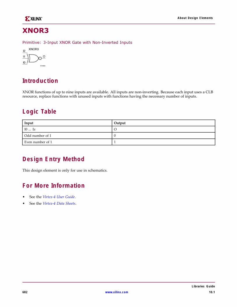
About Design Elements
XNOR3
Primitive: 3-Input XNOR Gate with Non-Inverted Inputs
IntroductionXNOR functions of up to nine inputs are available. All inputs are non-inverting. Because each input uses a CLBresource, replace functions with unused inputs with functions having the necessary number of inputs.
Logic TableInput Output
I0 ... Iz O
Odd number of 1 0
Even number of 1 1
Design Entry MethodThis design element is only for use in schematics.
For More Information• See the Virtex-4 User Guide.
• See the Virtex-4 Data Sheets.
Libraries Guide
682 www.xilinx.com 10.1
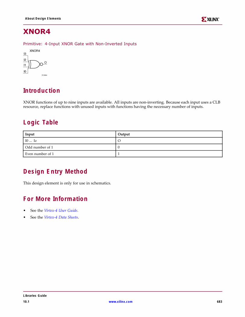
About Design Elements
XNOR4
Primitive: 4-Input XNOR Gate with Non-Inverted Inputs
IntroductionXNOR functions of up to nine inputs are available. All inputs are non-inverting. Because each input uses a CLBresource, replace functions with unused inputs with functions having the necessary number of inputs.
Logic TableInput Output
I0 ... Iz O
Odd number of 1 0
Even number of 1 1
Design Entry MethodThis design element is only for use in schematics.
For More Information• See the Virtex-4 User Guide.
• See the Virtex-4 Data Sheets.
Libraries Guide
10.1 www.xilinx.com 683
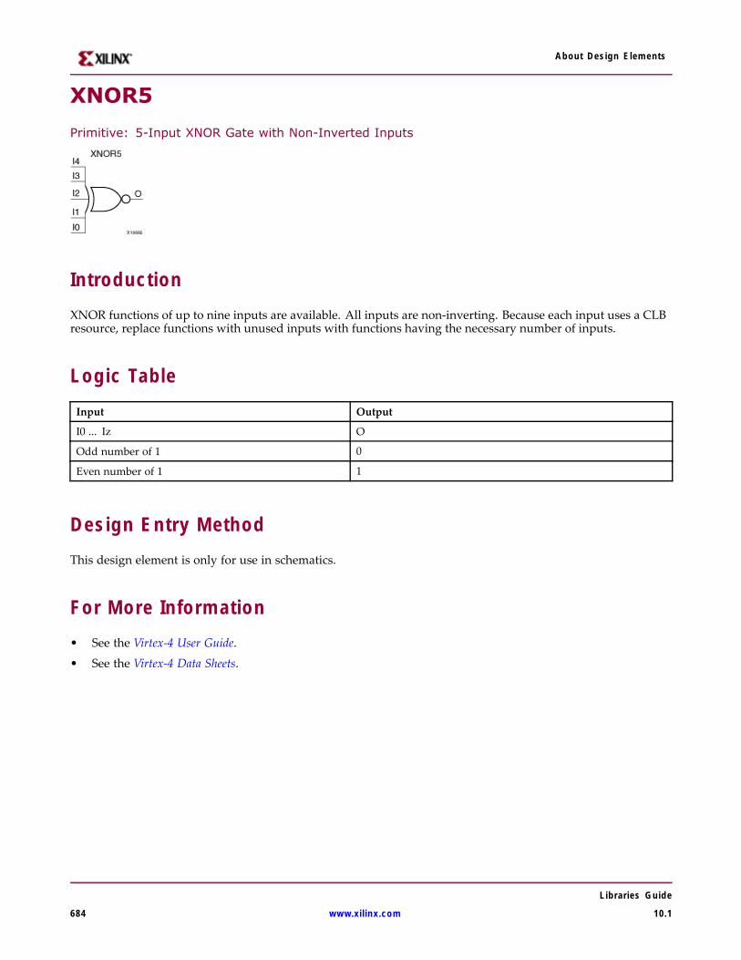
About Design Elements
XNOR5
Primitive: 5-Input XNOR Gate with Non-Inverted Inputs
IntroductionXNOR functions of up to nine inputs are available. All inputs are non-inverting. Because each input uses a CLBresource, replace functions with unused inputs with functions having the necessary number of inputs.
Logic TableInput Output
I0 ... Iz O
Odd number of 1 0
Even number of 1 1
Design Entry MethodThis design element is only for use in schematics.
For More Information• See the Virtex-4 User Guide.
• See the Virtex-4 Data Sheets.
Libraries Guide
684 www.xilinx.com 10.1
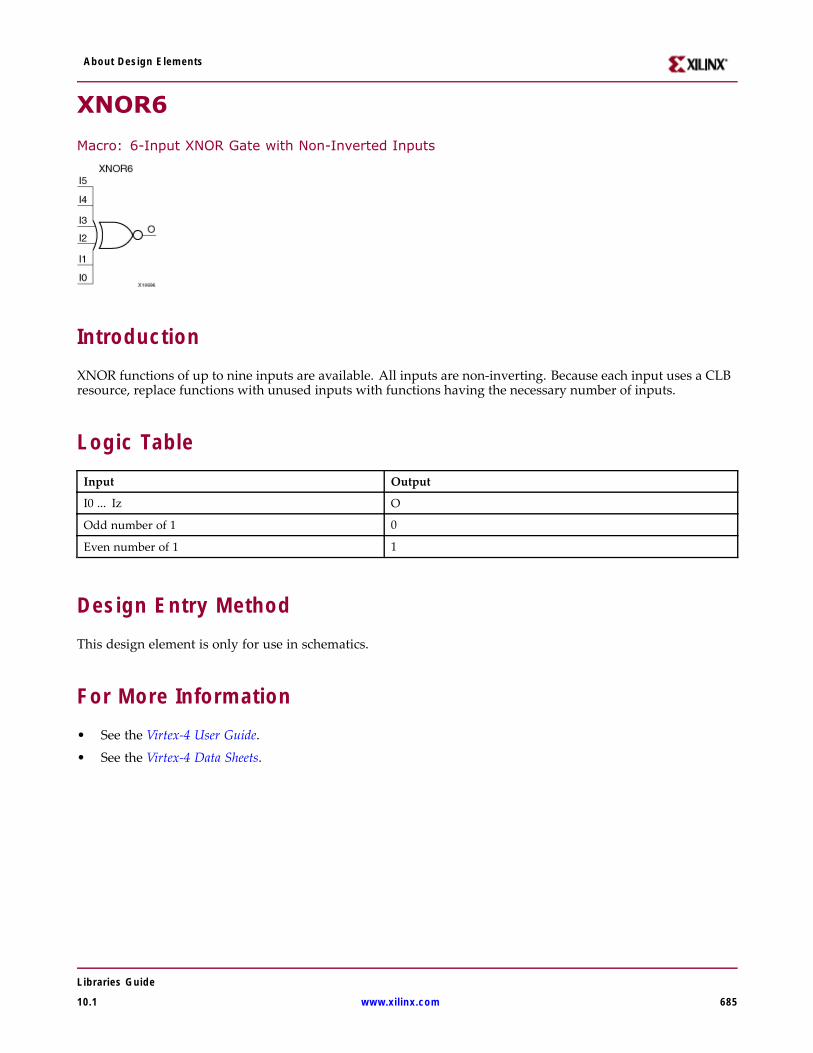
About Design Elements
XNOR6
Macro: 6-Input XNOR Gate with Non-Inverted Inputs
IntroductionXNOR functions of up to nine inputs are available. All inputs are non-inverting. Because each input uses a CLBresource, replace functions with unused inputs with functions having the necessary number of inputs.
Logic TableInput Output
I0 ... Iz O
Odd number of 1 0
Even number of 1 1
Design Entry MethodThis design element is only for use in schematics.
For More Information• See the Virtex-4 User Guide.
• See the Virtex-4 Data Sheets.
Libraries Guide
10.1 www.xilinx.com 685
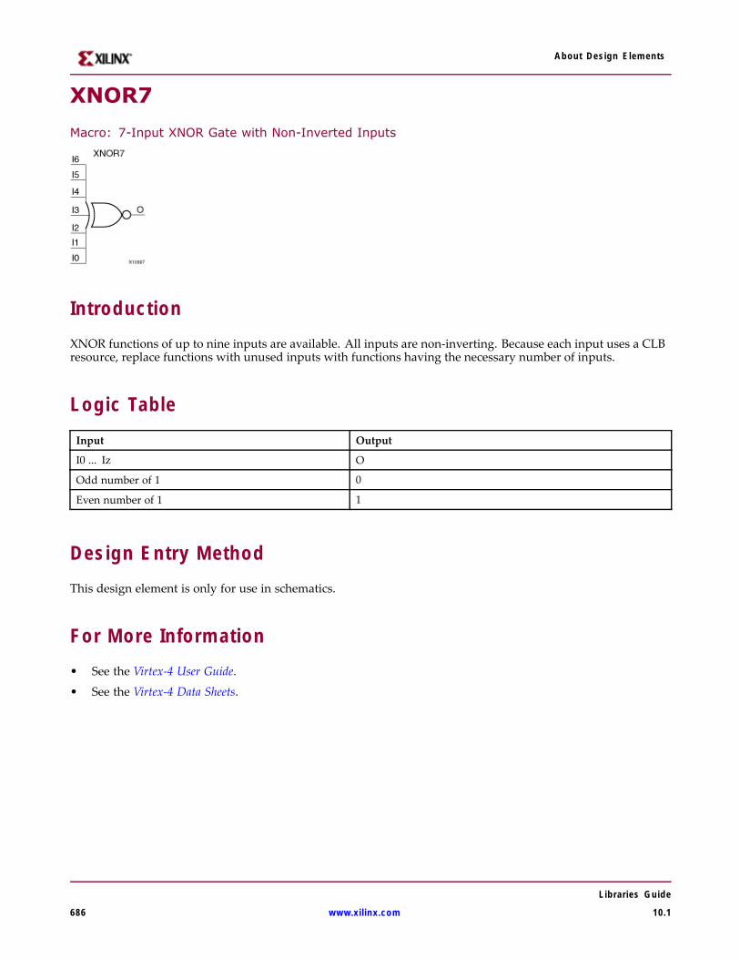
About Design Elements
XNOR7
Macro: 7-Input XNOR Gate with Non-Inverted Inputs
IntroductionXNOR functions of up to nine inputs are available. All inputs are non-inverting. Because each input uses a CLBresource, replace functions with unused inputs with functions having the necessary number of inputs.
Logic TableInput Output
I0 ... Iz O
Odd number of 1 0
Even number of 1 1
Design Entry MethodThis design element is only for use in schematics.
For More Information• See the Virtex-4 User Guide.
• See the Virtex-4 Data Sheets.
Libraries Guide
686 www.xilinx.com 10.1

About Design Elements
XNOR8
Macro: 8-Input XNOR Gate with Non-Inverted Inputs
IntroductionXNOR functions of up to nine inputs are available. All inputs are non-inverting. Because each input uses a CLBresource, replace functions with unused inputs with functions having the necessary number of inputs.
Logic TableInput Output
I0 ... Iz O
Odd number of 1 0
Even number of 1 1
Design Entry MethodThis design element is only for use in schematics.
For More Information• See the Virtex-4 User Guide.
• See the Virtex-4 Data Sheets.
Libraries Guide
10.1 www.xilinx.com 687
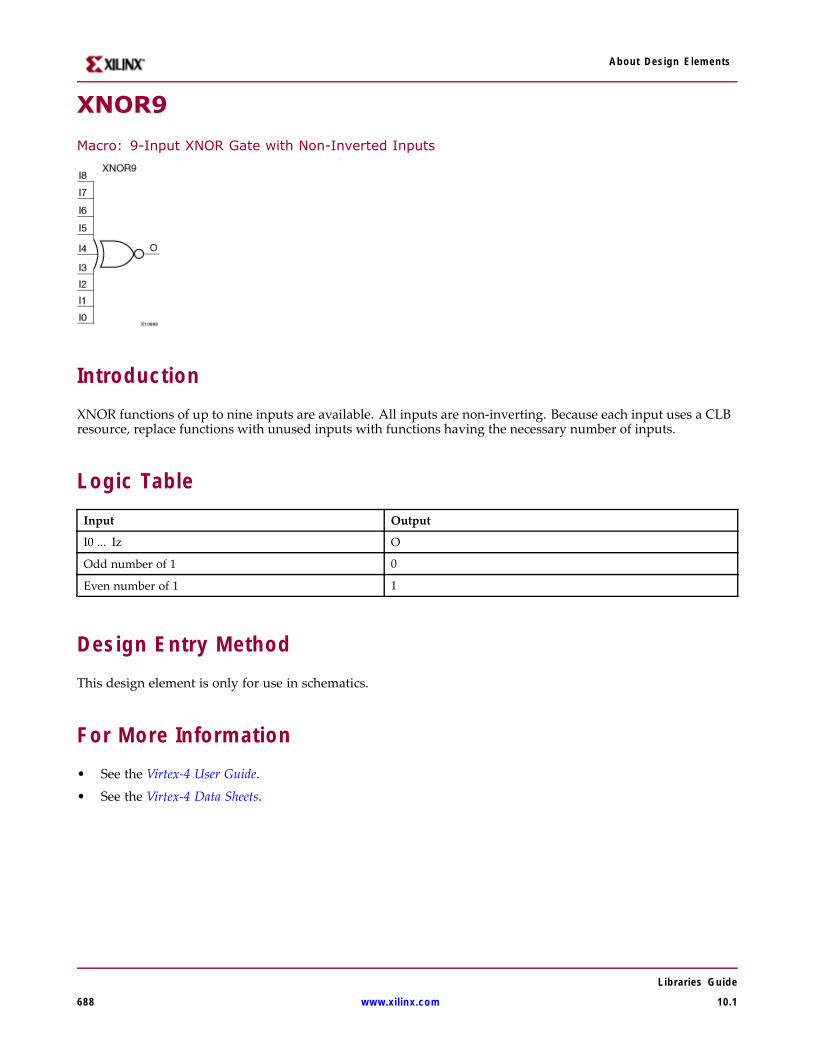
About Design Elements
XNOR9
Macro: 9-Input XNOR Gate with Non-Inverted Inputs
IntroductionXNOR functions of up to nine inputs are available. All inputs are non-inverting. Because each input uses a CLBresource, replace functions with unused inputs with functions having the necessary number of inputs.
Logic TableInput Output
I0 ... Iz O
Odd number of 1 0
Even number of 1 1
Design Entry MethodThis design element is only for use in schematics.
For More Information• See the Virtex-4 User Guide.
• See the Virtex-4 Data Sheets.
Libraries Guide
688 www.xilinx.com 10.1
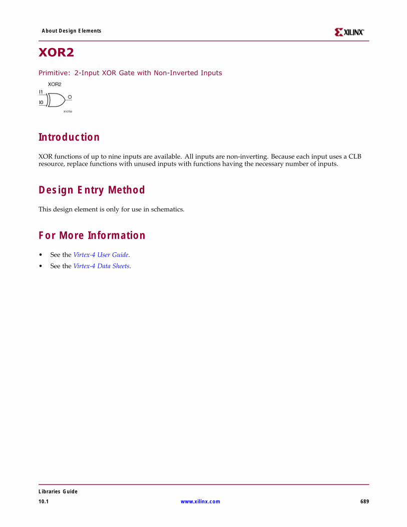
About Design Elements
XOR2
Primitive: 2-Input XOR Gate with Non-Inverted Inputs
IntroductionXOR functions of up to nine inputs are available. All inputs are non-inverting. Because each input uses a CLBresource, replace functions with unused inputs with functions having the necessary number of inputs.
Design Entry MethodThis design element is only for use in schematics.
For More Information• See the Virtex-4 User Guide.
• See the Virtex-4 Data Sheets.
Libraries Guide
10.1 www.xilinx.com 689
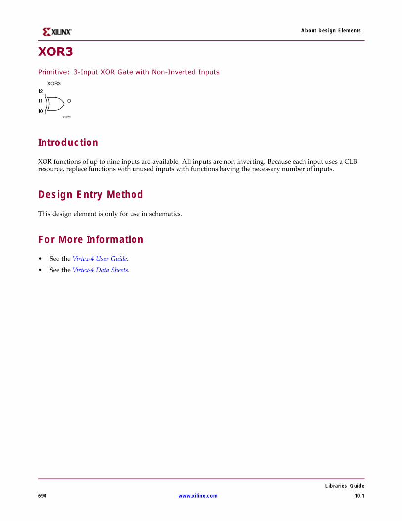
About Design Elements
XOR3
Primitive: 3-Input XOR Gate with Non-Inverted Inputs
IntroductionXOR functions of up to nine inputs are available. All inputs are non-inverting. Because each input uses a CLBresource, replace functions with unused inputs with functions having the necessary number of inputs.
Design Entry MethodThis design element is only for use in schematics.
For More Information• See the Virtex-4 User Guide.
• See the Virtex-4 Data Sheets.
Libraries Guide
690 www.xilinx.com 10.1
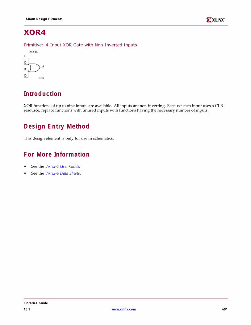
About Design Elements
XOR4
Primitive: 4-Input XOR Gate with Non-Inverted Inputs
IntroductionXOR functions of up to nine inputs are available. All inputs are non-inverting. Because each input uses a CLBresource, replace functions with unused inputs with functions having the necessary number of inputs.
Design Entry MethodThis design element is only for use in schematics.
For More Information• See the Virtex-4 User Guide.
• See the Virtex-4 Data Sheets.
Libraries Guide
10.1 www.xilinx.com 691
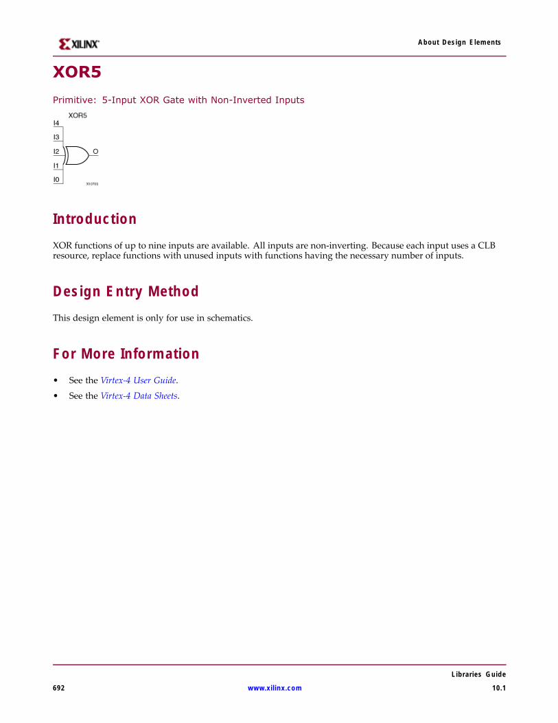
About Design Elements
XOR5
Primitive: 5-Input XOR Gate with Non-Inverted Inputs
IntroductionXOR functions of up to nine inputs are available. All inputs are non-inverting. Because each input uses a CLBresource, replace functions with unused inputs with functions having the necessary number of inputs.
Design Entry MethodThis design element is only for use in schematics.
For More Information• See the Virtex-4 User Guide.
• See the Virtex-4 Data Sheets.
Libraries Guide
692 www.xilinx.com 10.1
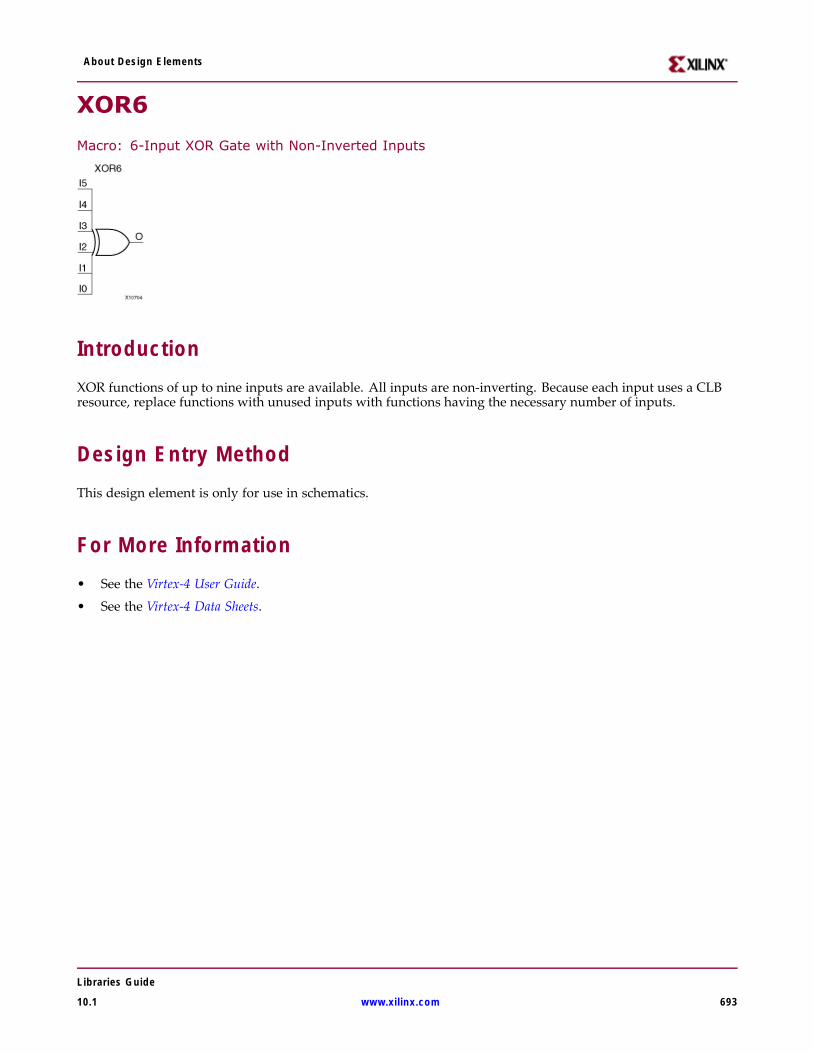
About Design Elements
XOR6
Macro: 6-Input XOR Gate with Non-Inverted Inputs
IntroductionXOR functions of up to nine inputs are available. All inputs are non-inverting. Because each input uses a CLBresource, replace functions with unused inputs with functions having the necessary number of inputs.
Design Entry MethodThis design element is only for use in schematics.
For More Information• See the Virtex-4 User Guide.
• See the Virtex-4 Data Sheets.
Libraries Guide
10.1 www.xilinx.com 693

About Design Elements
XOR7
Macro: 7-Input XOR Gate with Non-Inverted Inputs
IntroductionXOR functions of up to nine inputs are available. All inputs are non-inverting. Because each input uses a CLBresource, replace functions with unused inputs with functions having the necessary number of inputs.
Design Entry MethodThis design element is only for use in schematics.
For More Information• See the Virtex-4 User Guide.
• See the Virtex-4 Data Sheets.
Libraries Guide
694 www.xilinx.com 10.1
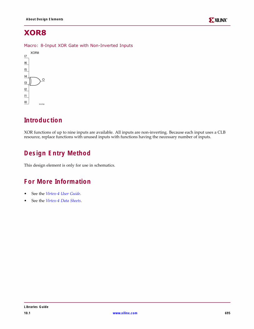
About Design Elements
XOR8
Macro: 8-Input XOR Gate with Non-Inverted Inputs
IntroductionXOR functions of up to nine inputs are available. All inputs are non-inverting. Because each input uses a CLBresource, replace functions with unused inputs with functions having the necessary number of inputs.
Design Entry MethodThis design element is only for use in schematics.
For More Information• See the Virtex-4 User Guide.
• See the Virtex-4 Data Sheets.
Libraries Guide
10.1 www.xilinx.com 695
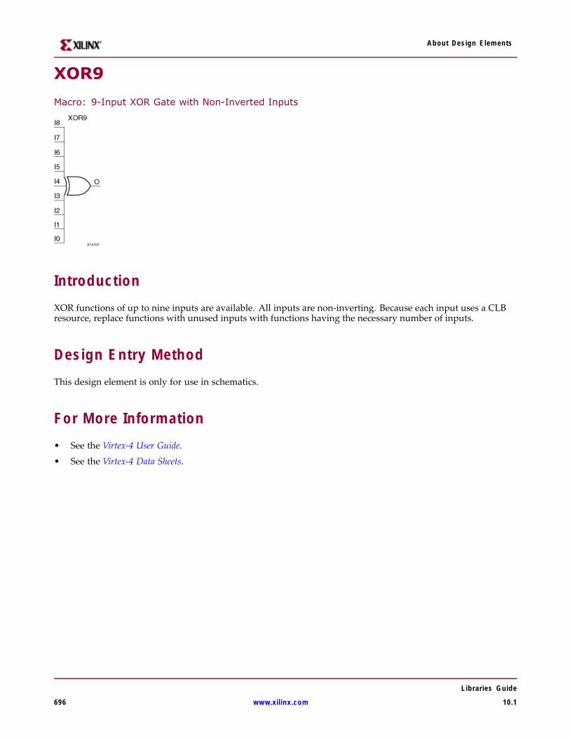
About Design Elements
XOR9
Macro: 9-Input XOR Gate with Non-Inverted Inputs
IntroductionXOR functions of up to nine inputs are available. All inputs are non-inverting. Because each input uses a CLBresource, replace functions with unused inputs with functions having the necessary number of inputs.
Design Entry MethodThis design element is only for use in schematics.
For More Information• See the Virtex-4 User Guide.
• See the Virtex-4 Data Sheets.
Libraries Guide
696 www.xilinx.com 10.1
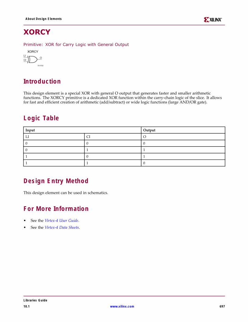
About Design Elements
XORCY
Primitive: XOR for Carry Logic with General Output
IntroductionThis design element is a special XOR with general O output that generates faster and smaller arithmeticfunctions. The XORCY primitive is a dedicated XOR function within the carry-chain logic of the slice. It allowsfor fast and efficient creation of arithmetic (add/subtract) or wide logic functions (large AND/OR gate).
Logic TableInput Output
LI CI O
0 0 0
0 1 1
1 0 1
1 1 0
Design Entry MethodThis design element can be used in schematics.
For More Information• See the Virtex-4 User Guide.
• See the Virtex-4 Data Sheets.
Libraries Guide
10.1 www.xilinx.com 697
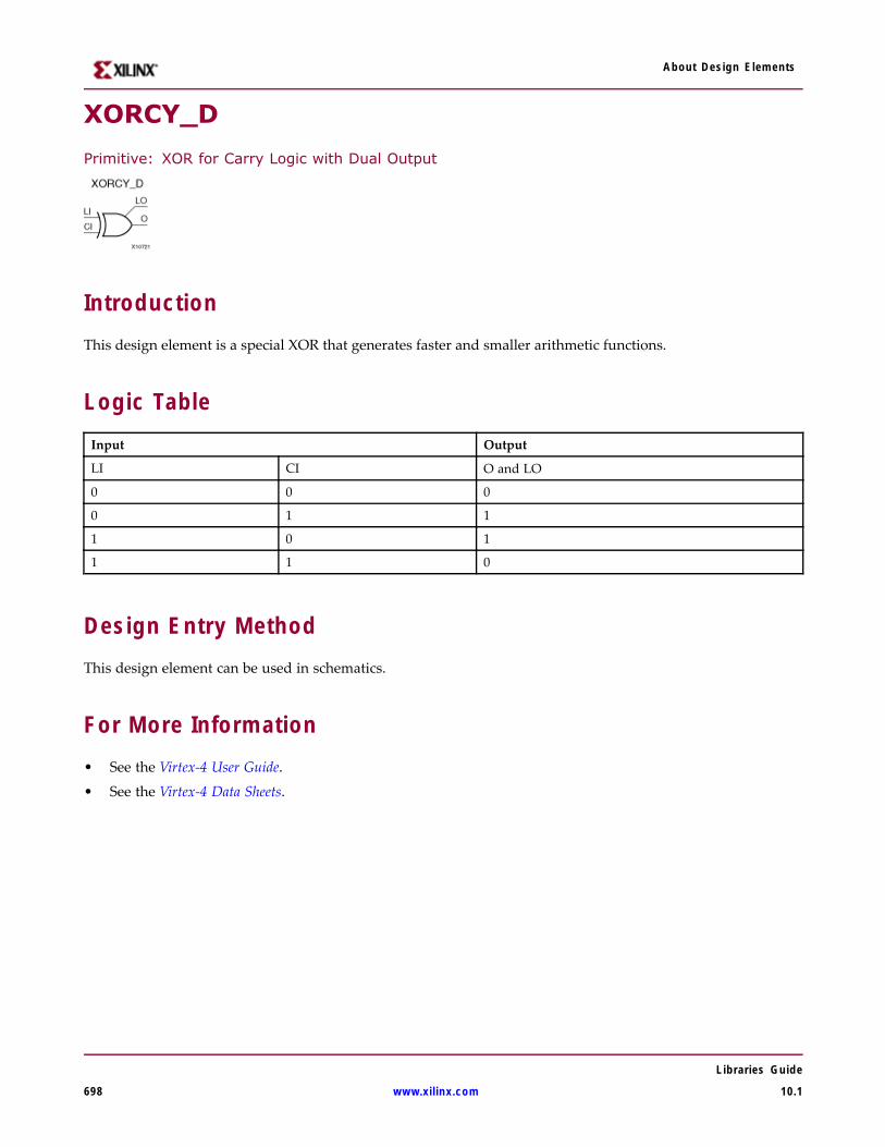
About Design Elements
XORCY_D
Primitive: XOR for Carry Logic with Dual Output
IntroductionThis design element is a special XOR that generates faster and smaller arithmetic functions.
Logic TableInput Output
LI CI O and LO
0 0 0
0 1 1
1 0 1
1 1 0
Design Entry MethodThis design element can be used in schematics.
For More Information• See the Virtex-4 User Guide.
• See the Virtex-4 Data Sheets.
Libraries Guide
698 www.xilinx.com 10.1
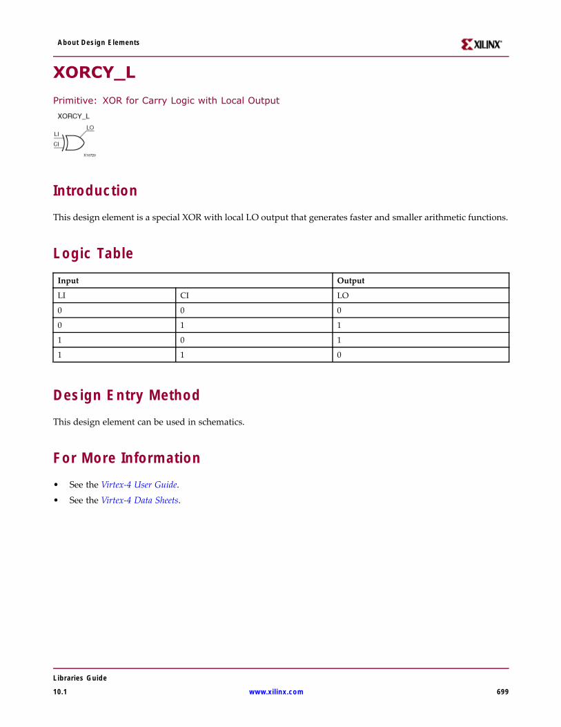
About Design Elements
XORCY_L
Primitive: XOR for Carry Logic with Local Output
IntroductionThis design element is a special XOR with local LO output that generates faster and smaller arithmetic functions.
Logic TableInput Output
LI CI LO
0 0 0
0 1 1
1 0 1
1 1 0
Design Entry MethodThis design element can be used in schematics.
For More Information• See the Virtex-4 User Guide.
• See the Virtex-4 Data Sheets.
Libraries Guide
10.1 www.xilinx.com 699