Embed Size (px)
Citation preview
SensL © 2013 1
ArrayC PCB Arrays of SiPMUSER MANUAL
4-Side Scaleable SiPM Arrays
SensL’s custom range of C-Series, SMT (surface mount technology) SiPM sensors have been used to create compact and scaleable arrays. The sensors are mounted onto PCB boards with minimal dead space. The ArrayC products are available in a variety of formats, and formed of pixels of different sizes. Details of the arrays available are given in the Ordering Information table on the final page of this document.
The back of each ArrayC has either one or more multi-way connectors, or a BGA (ball grid array), that allow access to the fast output* and standard I/O from each pixel in the array, and a common I/O from the summed substrates of the pixels. The ArrayC products with connectors can be used to interface with the user’s own readout via the mating connector, or to SensL’s Breakout Boards (BOBs). The BOBs allow for easy access to the pixel signals and performance evaluation of the arrays.
ArrayC products with the BGA can be reflow soldered to the user’s readout boards, or purchased ready-mounted on an Evaluation Board (EVB) for easy testing. The BGA ArrayC products cannot be removed from their EVBs. This contrasts with an ArrayC that has connectors, where multiple arrays can be evaluated with a single BOB.
Array Inputs and Outputs (I/O)
Figure 1 summarizes the array schematic for a portion of an ArrayC. Each SiPM sensor in the array has three electrical connections: fast output*, standard output and common.
The substrates (cathodes) of all sensors are summed together to form the common I/O.
Each individual fast output* and standard I/O (anode) are routed to its own output pin.
The pixel-level performance of the sensors in the array can be found in the C-Series datasheet.
Figure 1, Signal connections at the pixel level of an ArrayC
* The ArrayC-60035-4P does not have access to the fast output.
SensL © 2013 2
ArrayC PCB Arrays of SiPMUSER MANUAL
SensL © 2013 2
ArrayC PCB Arrays of SiPMUSER MANUAL
CONTENTS
ArrayC-60035-4P-BGA (2x2 Array of 6mm SMT Sensors) ...........................................................................................4
Schematics for the ArrayC-60035-4P-BGA .............................................................................................................................. 4
BGA Connections for the ArrayC-60035-4P-BGA .................................................................................................................... 5
ArrayC-60035-4P-BGA - Solder Footprint and Reflow Solder Profile ........................................................................................ 5
ArrayC-60035-4P-EVB (ArrayC-60035-4P-BGA Evaluation Board) ......................................................................................... 6
Schematics for the ArrayC-60035-4P-EVB ............................................................................................................................... 6
ArrayC-60035-4P-EVB Pin-Outs .............................................................................................................................................. 6
ArrayC-60035-64P-PCB (8x8 Array of 6mm SMT Sensors) .........................................................................................7
Schematics for the ArrayC-60035-64P-PCB ............................................................................................................................ 7
Connector Schematic for the ArrayC-60035-64P-PCB ............................................................................................................. 8
Connector Pin-Outs for the ArrayC-60035-64P-PCB ............................................................................................................... 9
ArrayX-BOB6-64P (ArrayC-60035-64P Breakout Board) ...................................................................................................... 10
Header Signals on the ArrayX-BOB6-64P ............................................................................................................................... 11
ArrayX-BOB6-64S (Summed Breakout Board for the ArrayC-60035-64P) ............................................................................. 12
Header Signals on the ArrayX-BOB6-64S ............................................................................................................................... 13
ArrayC-30035-16P-PCB (4x4 Array of 3mm SMT Sensors) .......................................................................................14
Schematics for the ArrayC-30035-16P-PCB .......................................................................................................................... 14
Connector Pin-Outs for the ArrayC-30035-16P-PCB ............................................................................................................. 15
ArrayX-BOB3-16P (ArrayC-30035-16P Breakout Board) ........................................................................................................ 16
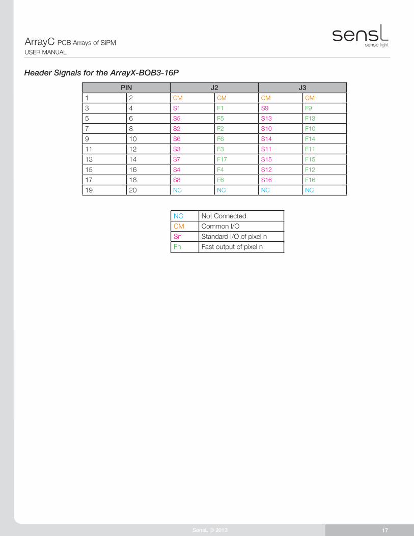
Header Signals for the ArrayX-BOB3-16P .............................................................................................................................. 17
ArrayX-BOB3-16S (Summed Breakout Board for the ArrayC-30035-16P) .............................................................................. 18
Header Signals for the ArrayX-BOB3-16S .............................................................................................................................. 19
ArrayC-30035-144P-PCB (12x12 Array of 3mm SMT Sensors) .................................................................................20
Schematics for the ArrayC-30035-144P-PCB ........................................................................................................................ 20
Connector Schematics for the ArrayC-30035-144P ............................................................................................................... 21
Connector Pin-Outs for the ArrayC-30035-144P .................................................................................................................... 22
ArrayX-BOB3-144P (ArrayC-30035-144P Breakout Board) .................................................................................................... 24
Header Signals for the ArrayX-BOB3-144P ............................................................................................................................ 25
ArrayC-10035-64P-BGA (8x8 Array of 1mm SMT Sensors) .......................................................................................26
Schematics for the ArrayC-10035-64P-BGA .......................................................................................................................... 26
BGA Connections for the ArrayC-10035-64P-BGA ................................................................................................................ 27
ArrayC-10035-64P-BGA Reflow Solder Profile ....................................................................................................................... 27
ArrayC-10035-64P-EVB (Evaluation Board with ArrayC-10035-64P-BGA Attached) .............................................................. 28
Header Signals for the ArrayC-10035-64P-EVB ..................................................................................................................... 29
Biasing and Readout from the Standard Breakout Boards ........................................................................................30
SMA Connector ..................................................................................................................................................................... 30
Balun Transformer .................................................................................................................................................................. 30
EMI Considerations ................................................................................................................................................................ 31
Appendix A - Example of Using the Breakout Board to readout Fast signals ..............................................................32
Appendix B - Example of Using the Breakout Board to readout Standard signals ......................................................33
Appendix C - Example of Using the SUMMED Breakout Board ................................................................................34
Ordering Information ..................................................................................................................................................35
SensL © 2013 3
ArrayC PCB Arrays of SiPMUSER MANUAL
SensL © 2013 3
ArrayC PCB Arrays of SiPMUSER MANUAL
ATTENTION!
Great care should be taken when disconnecting the ArrayC PCBs from the mating connectors, either on one of the BOBs, or the user’s own boards.
The board should be gently levered up, working progressively around the board to lever the PCB from the connector a little on all sides, and then repeating the process until the connectors are free from each other.
Note that a BGA ArrayC cannot be removed from its EVB.
SensL © 2013 4
ArrayC PCB Arrays of SiPMUSER MANUAL
SensL © 2013 4
ArrayC PCB Arrays of SiPMUSER MANUAL
ARRAYC-60035-4P-BGA (2X2 ARRAY OF 6MM SMT SENSORS)
Array Size
Sensor type
Readout Board SizePixel Pitch
No. Connections
No. Connectors
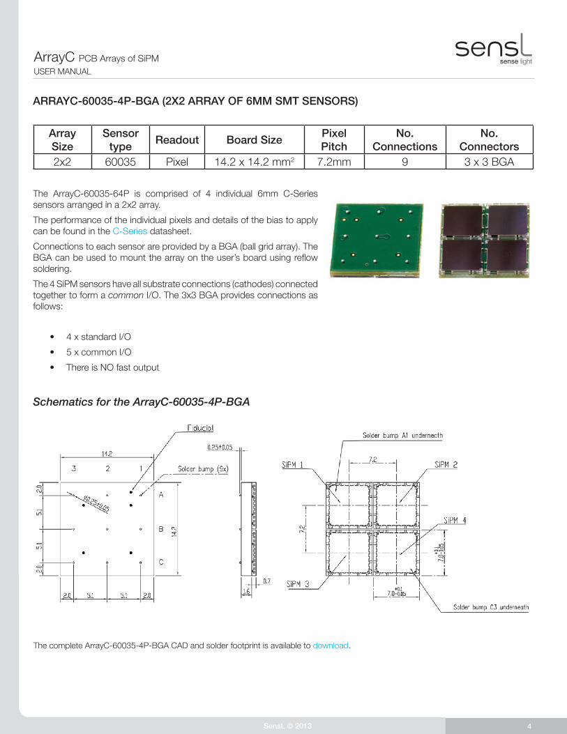
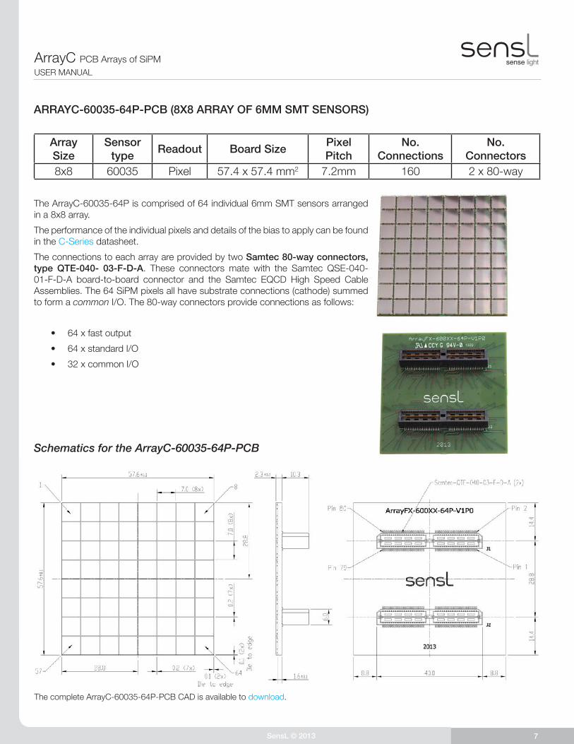
2x2 60035 Pixel 14.2 x 14.2 mm2 7.2mm 9 3 x 3 BGA
The ArrayC-60035-64P is comprised of 4 individual 6mm C-Series sensors arranged in a 2x2 array.
The performance of the individual pixels and details of the bias to apply can be found in the C-Series datasheet.
Connections to each sensor are provided by a BGA (ball grid array). The BGA can be used to mount the array on the user’s board using reflow soldering.
The 4 SiPM sensors have all substrate connections (cathodes) connected together to form a common I/O. The 3x3 BGA provides connections as follows:
• 4 x standard I/O
• 5 x common I/O
• There is NO fast output
Schematics for the ArrayC-60035-4P-BGA
The complete ArrayC-60035-4P-BGA CAD and solder footprint is available to download.
SensL © 2013 5
ArrayC PCB Arrays of SiPMUSER MANUAL
SensL © 2013 5
ArrayC PCB Arrays of SiPMUSER MANUAL
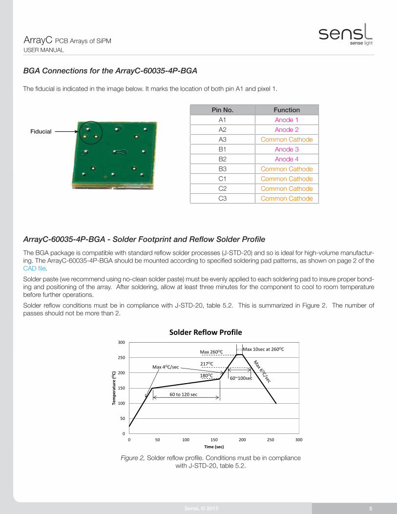
BGA Connections for the ArrayC-60035-4P-BGA
Pin No. Function
A1 Anode 1
A2 Anode 2
A3 Common Cathode
B1 Anode 3
B2 Anode 4
B3 Common Cathode
C1 Common Cathode
C2 Common Cathode
C3 Common Cathode
ArrayC-60035-4P-BGA - Solder Footprint and Reflow Solder Profile
The BGA package is compatible with standard reflow solder processes (J-STD-20) and so is ideal for high-volume manufactur-ing. The ArrayC-60035-4P-BGA should be mounted according to specified soldering pad patterns, as shown on page 2 of the CAD file.
Solder paste (we recommend using no-clean solder paste) must be evenly applied to each soldering pad to insure proper bond-ing and positioning of the array. After soldering, allow at least three minutes for the component to cool to room temperature before further operations.
Solder reflow conditions must be in compliance with J-STD-20, table 5.2. This is summarized in Figure 2. The number of passes should not be more than 2.
0
50
100
150
200
250
300
0 50 100 150 200 250 300
Tem
pera
ture
(OC)
Time (sec)
Solder Reflow Profile
Max 4OC/sec
60 to 120 sec
Max 260OC
217OC
180OC 60~100sec
Max 10sec at 260OC
Figure 2, Solder reflow profile. Conditions must be in compliance with J-STD-20, table 5.2.
Fiducial
The fiducial is indicated in the image below. It marks the location of both pin A1 and pixel 1.
SensL © 2013 6
ArrayC PCB Arrays of SiPMUSER MANUAL
SensL © 2013 6
ArrayC PCB Arrays of SiPMUSER MANUAL
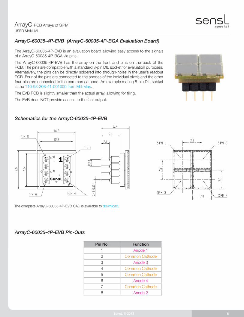
ArrayC-60035-4P-EVB (ArrayC-60035-4P-BGA Evaluation Board)
The ArrayC-60035-4P-EVB is an evaluation board allowing easy access to the signals of a ArrayC-60035-4P-BGA via pins.
The ArrayC-60035-4P-EVB has the array on the front and pins on the back of the PCB. The pins are compatible with a standard 8-pin DIL socket for evaluation purposes. Alternatively, the pins can be directly soldered into through-holes in the user’s readout PCB. Four of the pins are connected to the anodes of the individual pixels and the other four pins are connected to the common cathode. An example mating 8-pin DIL socket is the 110-93-308-41-001000 from Mill-Max.
The EVB PCB is slightly smaller than the actual array, allowing for tiling.
The EVB does NOT provide access to the fast output.
Schematics for the ArrayC-60035-4P-EVB
ArrayC-60035-4P-EVB Pin-Outs
Pin No. Function
1 Anode 1
2 Common Cathode
3 Anode 3
4 Common Cathode
5 Common Cathode
6 Anode 4
7 Common Cathode
8 Anode 2
The complete ArrayC-60035-4P-EVB CAD is available to download.
SensL © 2013 7
ArrayC PCB Arrays of SiPMUSER MANUAL
SensL © 2013 7
ArrayC PCB Arrays of SiPMUSER MANUAL
ARRAYC-60035-64P-PCB (8X8 ARRAY OF 6MM SMT SENSORS)
Array Size
Sensor type
Readout Board SizePixel Pitch
No. Connections
No. Connectors
8x8 60035 Pixel 57.4 x 57.4 mm2 7.2mm 160 2 x 80-way
The ArrayC-60035-64P is comprised of 64 individual 6mm SMT sensors arranged in a 8x8 array.
The performance of the individual pixels and details of the bias to apply can be found in the C-Series datasheet.
The connections to each array are provided by two Samtec 80-way connectors, type QTE-040- 03-F-D-A. These connectors mate with the Samtec QSE-040-01-F-D-A board-to-board connector and the Samtec EQCD High Speed Cable Assemblies. The 64 SiPM pixels all have substrate connections (cathode) summed to form a common I/O. The 80-way connectors provide connections as follows:
• 64 x fast output
• 64 x standard I/O
• 32 x common I/O
Schematics for the ArrayC-60035-64P-PCB
The complete ArrayC-60035-64P-PCB CAD is available to download.
SensL © 2013 8
ArrayC PCB Arrays of SiPMUSER MANUAL
SensL © 2013 8
ArrayC PCB Arrays of SiPMUSER MANUAL
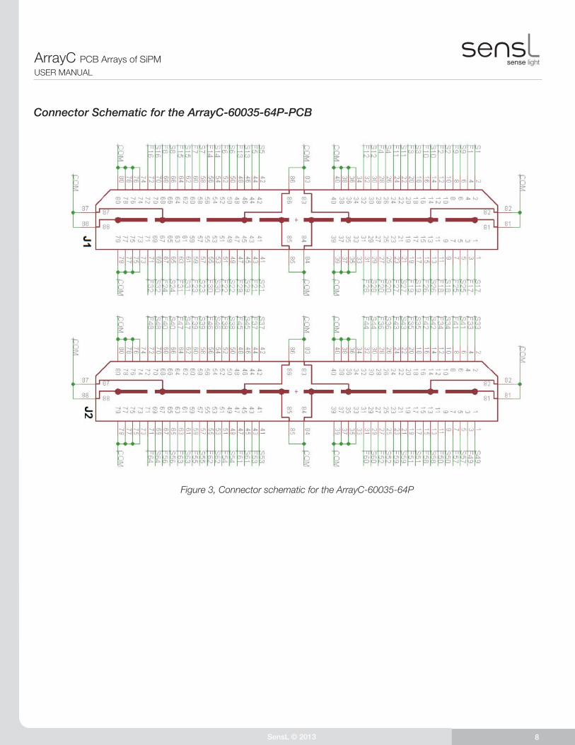
Connector Schematic for the ArrayC-60035-64P-PCB
Figure 3, Connector schematic for the ArrayC-60035-64P
SensL © 2013 9
ArrayC PCB Arrays of SiPMUSER MANUAL
SensL © 2013 9
ArrayC PCB Arrays of SiPMUSER MANUAL
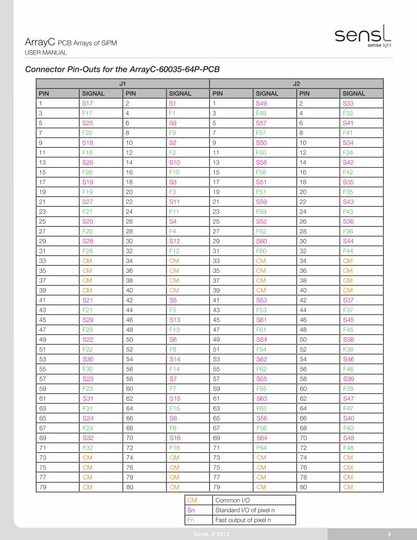
Connector Pin-Outs for the ArrayC-60035-64P-PCB
J1 J2
PIN SIGNAL PIN SIGNAL PIN SIGNAL PIN SIGNAL
1 S17 2 S1 1 S49 2 S33
3 F17 4 F1 3 F49 4 F33
5 S25 6 S9 5 S57 6 S41
7 F25 8 F9 7 F57 8 F41
9 S18 10 S2 9 S50 10 S34
11 F18 12 F2 11 F50 12 F34
13 S26 14 S10 13 S58 14 S42
15 F26 16 F10 15 F58 16 F42
17 S19 18 S3 17 S51 18 S35
19 F19 20 F3 19 F51 20 F35
21 S27 22 S11 21 S59 22 S43
23 F27 24 F11 23 F59 24 F43
25 S20 26 S4 25 S52 26 S36
27 F20 28 F4 27 F52 28 F36
29 S28 30 S12 29 S60 30 S44
31 F28 32 F12 31 F60 32 F44
33 CM 34 CM 33 CM 34 CM
35 CM 36 CM 35 CM 36 CM
37 CM 38 CM 37 CM 38 CM
39 CM 40 CM 39 CM 40 CM
41 S21 42 S5 41 S53 42 S37
43 F21 44 F5 43 F53 44 F37
45 S29 46 S13 45 S61 46 S45
47 F29 48 F13 47 F61 48 F45
49 S22 50 S6 49 S54 50 S38
51 F22 52 F6 51 F54 52 F38
53 S30 54 S14 53 S62 54 S46
55 F30 56 F14 55 F62 56 F46
57 S23 58 S7 57 S55 58 S39
59 F23 60 F7 59 F55 60 F39
61 S31 62 S15 61 S63 62 S47
63 F31 64 F15 63 F63 64 F47
65 S24 66 S8 65 S56 66 S40
67 F24 68 F8 67 F56 68 F40
69 S32 70 S16 69 S64 70 S48
71 F32 72 F16 71 F64 72 F48
73 CM 74 CM 73 CM 74 CM
75 CM 76 CM 75 CM 76 CM
77 CM 78 CM 77 CM 78 CM
79 CM 80 CM 79 CM 80 CM
CM Common I/O
Sn Standard I/O of pixel n
Fn Fast output of pixel n
SensL © 2013 10
ArrayC PCB Arrays of SiPMUSER MANUAL
SensL © 2013 10
ArrayC PCB Arrays of SiPMUSER MANUAL
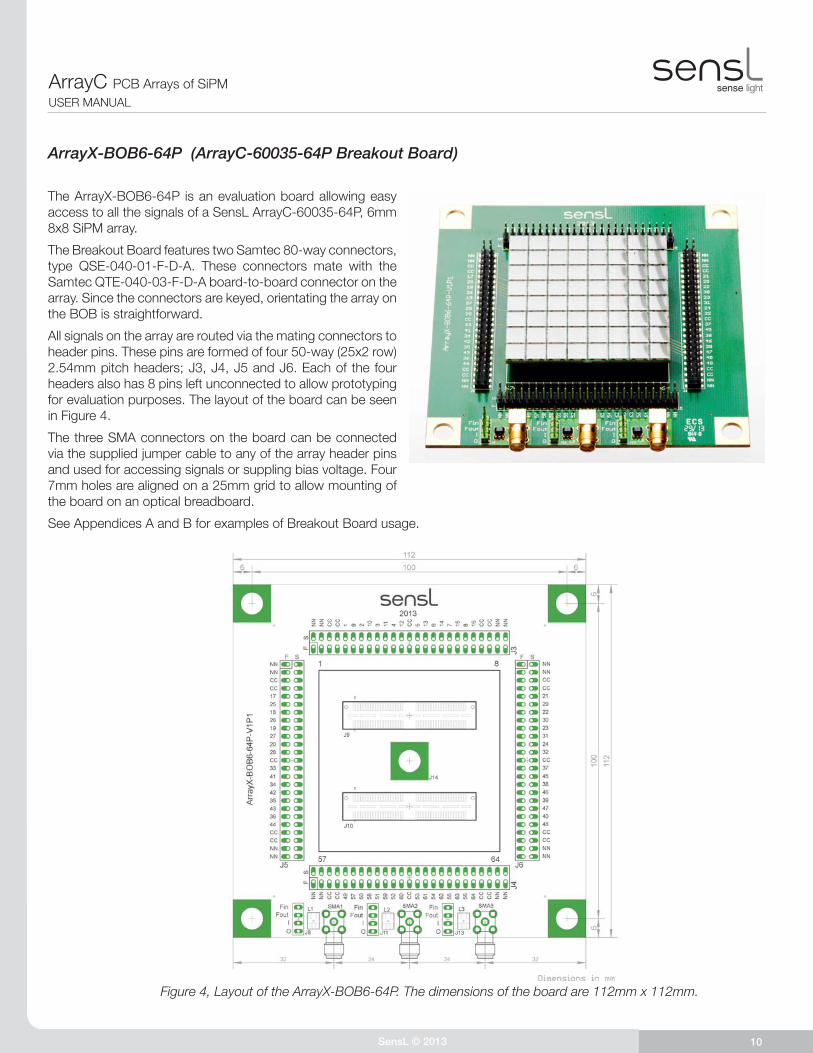
ArrayX-BOB6-64P (ArrayC-60035-64P Breakout Board)
The ArrayX-BOB6-64P is an evaluation board allowing easy access to all the signals of a SensL ArrayC-60035-64P, 6mm 8x8 SiPM array.
The Breakout Board features two Samtec 80-way connectors, type QSE-040-01-F-D-A. These connectors mate with the Samtec QTE-040-03-F-D-A board-to-board connector on the array. Since the connectors are keyed, orientating the array on the BOB is straightforward.
All signals on the array are routed via the mating connectors to header pins. These pins are formed of four 50-way (25x2 row) 2.54mm pitch headers; J3, J4, J5 and J6. Each of the four headers also has 8 pins left unconnected to allow prototyping for evaluation purposes. The layout of the board can be seen in Figure 4.
The three SMA connectors on the board can be connected via the supplied jumper cable to any of the array header pins and used for accessing signals or suppling bias voltage. Four 7mm holes are aligned on a 25mm grid to allow mounting of the board on an optical breadboard.
See Appendices A and B for examples of Breakout Board usage.
Figure 4, Layout of the ArrayX-BOB6-64P. The dimensions of the board are 112mm x 112mm.
SensL © 2013 11
ArrayC PCB Arrays of SiPMUSER MANUAL
SensL © 2013 11
ArrayC PCB Arrays of SiPMUSER MANUAL
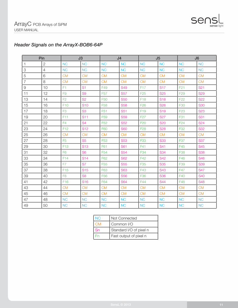
Pin J3 J4 J5 J6
1 2 NC NC NC NC NC NC NC NC
3 4 NC NC NC NC NC NC NC NC
5 6 CM CM CM CM CM CM CM CM
7 8 CM CM CM CM CM CM CM CM
9 10 F1 S1 F49 S49 F17 S17 F21 S21
11 12 F9 S9 F57 S57 F25 S25 F29 S29
13 14 F2 S2 F50 S50 F18 S18 F22 S22
15 16 F10 S10 F58 S58 F26 S26 F30 S30
17 18 F3 S3 F51 S51 F19 S19 F23 S23
19 20 F11 S11 F59 S59 F27 S27 F31 S31
21 22 F4 S4 F52 S52 F20 S20 F24 S24
23 24 F12 S12 F60 S60 F28 S28 F32 S32
25 26 CM CM CM CM CM CM CM CM
27 28 F5 S5 F53 S53 F33 S33 F37 S37
29 30 F13 S13 F61 S61 F41 S41 F45 S45
31 32 F6 S6 F54 S54 F34 S34 F38 S38
33 34 F14 S14 F62 S62 F42 S42 F46 S46
35 36 F7 S7 F55 S55 F35 S35 F39 S39
37 38 F15 S15 F63 S63 F43 S43 F47 S47
39 40 F8 S8 F56 S56 F36 S36 F40 S40
41 42 F16 S16 F64 S64 F44 S44 F48 S48
43 44 CM CM CM CM CM CM CM CM
45 46 CM CM CM CM CM CM CM CM
47 48 NC NC NC NC NC NC NC NC
49 50 NC NC NC NC NC NC NC NC
Header Signals on the ArrayX-BOB6-64P
NC Not Connected
CM Common I/O
Sn Standard I/O of pixel n
Fn Fast output of pixel n
SensL © 2013 12
ArrayC PCB Arrays of SiPMUSER MANUAL
SensL © 2013 12
ArrayC PCB Arrays of SiPMUSER MANUAL
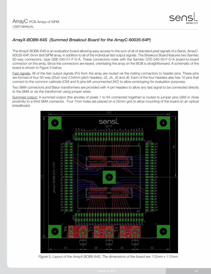
ArrayX-BOB6-64S (Summed Breakout Board for the ArrayC-60035-64P)
The ArrayX-BOB6-64S is an evaluation board allowing easy access to the sum of all of standard pixel signals of a SensL ArrayC-60035-64P, 6mm 8x8 SiPM array, in addition to all of the individual fast output signals. The Breakout Board features two Samtec 80-way connectors, type QSE-040-01-F-D-A. These connectors mate with the Samtec QTE-040-03-F-D-A board-to-board connector on the array. Since the connectors are keyed, orientating the array on the BOB is straightforward. A schematic of the board is shown in Figure 5 below.
Fast signals: All of the fast output signals (Fn) from the array are routed via the mating connectors to header pins. These pins are formed of four 50-way (25x2 row) 2.54mm pitch headers; J3, J4, J5 and J6. Each of the four headers also has 10 pins that connect to the common cathode (CM) and 8 pins left unconnected (NC) to allow prototyping for evaluation purposes.
Two SMA connectors and Balun transformers are provided with 4-pin headers to allow any fast signal to be connected directly to the SMA or via the transformer using jumper wires.
Summed output: A summed output (the anodes of pixels 1 to 64 connected together) is routed to jumper pins (SM) in close proximity to a third SMA connector. Four 7mm holes are placed on a 25mm grid to allow mounting of the board on an optical breadboard.
Figure 5, Layout of the ArrayX-BOB6-64S. The dimensions of the board are 112mm x 112mm.
SensL © 2013 13
ArrayC PCB Arrays of SiPMUSER MANUAL
SensL © 2013 13
ArrayC PCB Arrays of SiPMUSER MANUAL
Pin J3 J4 J5 J6
1 2 CM CM CM CM CM CM CM CM
3 4 CM CM CM CM CM CM CM CM
5 6 NC NC NC NC NC NC NC NC
7 8 NC NC NC NC NC NC NC NC
9 10 F1 F1 F49 F49 F17 F17 F21 F21
11 12 F9 F9 F57 F57 F25 F25 F29 F29
13 14 F2 F2 F50 F50 F18 F18 F22 F22
15 16 F10 F10 F58 F58 F26 F26 F30 F30
17 18 F3 F3 F51 F51 F19 F19 F23 F23
19 20 F11 F11 F59 F59 F27 F27 F31 F31
21 22 F4 F4 F52 F52 F20 F20 F24 F24
23 24 F12 F12 F60 F60 F28 F28 F32 F32
25 26 CM CM CM CM CM CM CM CM
27 28 F5 F5 F53 F53 F33 F33 F37 F37
29 30 F13 F13 F61 F61 F41 F41 F45 F45
31 32 F6 F6 F54 F54 F34 F34 F38 F38
33 34 F14 F14 F62 F62 F42 F42 F46 F46
35 36 F7 F7 F55 F55 F35 F35 F39 F39
37 38 F15 F15 F63 F63 F43 F43 F47 F47
39 40 F8 F8 F56 F56 F36 F36 F40 F40
41 42 F16 F16 F64 F64 F44 F44 F48 F48
43 44 NC NC NC NC NC NC NC NC
45 46 NC NC NC NC NC NC NC NC
47 48 CM CM CM CM CM CM CM CM
49 50 CM CM CM CM CM CM CM CM
Header Signals on the ArrayX-BOB6-64S
NC Not Connected
CM Common cathode I/O
Fn Fast output of pixel n
SensL © 2013 14
ArrayC PCB Arrays of SiPMUSER MANUAL
SensL © 2013 14
ArrayC PCB Arrays of SiPMUSER MANUAL
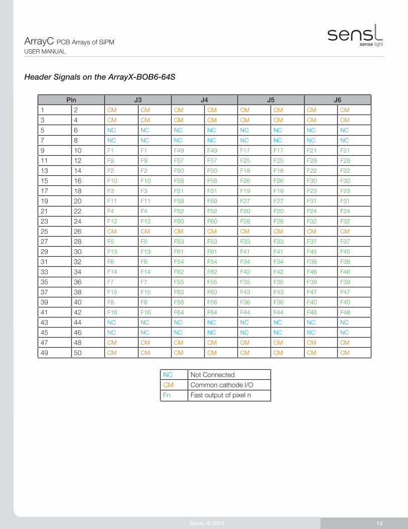
ARRAYC-30035-16P-PCB (4X4 ARRAY OF 3MM SMT SENSORS)
Array Size
Sensor type
Readout Pixel Pitch Board SizeNo.
ConnectionsNo.
Connectors4x4 30035 Pixel 4.2mm 16.6 x 16.6 mm2 40 1 x 40-way
The ArrayC-30035-16P-PCB is comprised of 16 individual 3mm C-Series sensors arranged in a 4x4 array.
The performance of the individual pixels and details of the bias to apply can be found in the C-Series datasheet.
Connections to each sensor are provided by a 40-way Hirose plug-type board-to-board connector DF17(2.0)-40DP-0.5V(57). These connectors mate with the Hirose DF17(3.0)-40DS-0.5V(57). The 16 SiPM pixels have all substrates (cathodes) connected together to form a common I/O. The 40-way connector provides connections as follows:
• 16 x fast output
• 16 x standard I/O
• 8 x common I/O
Schematics for the ArrayC-30035-16P-PCB
The complete ArrayC-30035-16P-PCB CAD is available to download.
SensL © 2013 15
ArrayC PCB Arrays of SiPMUSER MANUAL
SensL © 2013 15
ArrayC PCB Arrays of SiPMUSER MANUAL
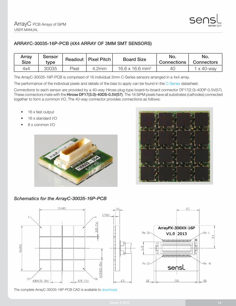
Connector Pin-Outs for the ArrayC-30035-16P-PCB
Figure 6, Connector pin-outs for the ArrayC-30035-16P
Pin Signal Pin Signal
1 CM 40 CM
2 CM 39 CM
3 S1 38 S9
4 F1 37 F9
5 S5 36 S13
6 F5 35 F13
7 S2 34 S10
8 F2 33 F10
9 S6 32 S14
10 F6 31 F14
11 S3 30 S11
12 F3 29 F11
13 S7 28 S15
14 F7 27 F15
15 S4 26 S12
16 F4 25 F12
17 S8 24 S16
18 F8 23 F16
19 CM 22 CM
20 CM 21 CM
CM Common I/O
Sn Standard I/O of pixel n
Fn Fast output of pixel n
SensL © 2013 16
ArrayC PCB Arrays of SiPMUSER MANUAL
SensL © 2013 16
ArrayC PCB Arrays of SiPMUSER MANUAL
ArrayX-BOB3-16P (ArrayC-30035-16P Breakout Board)
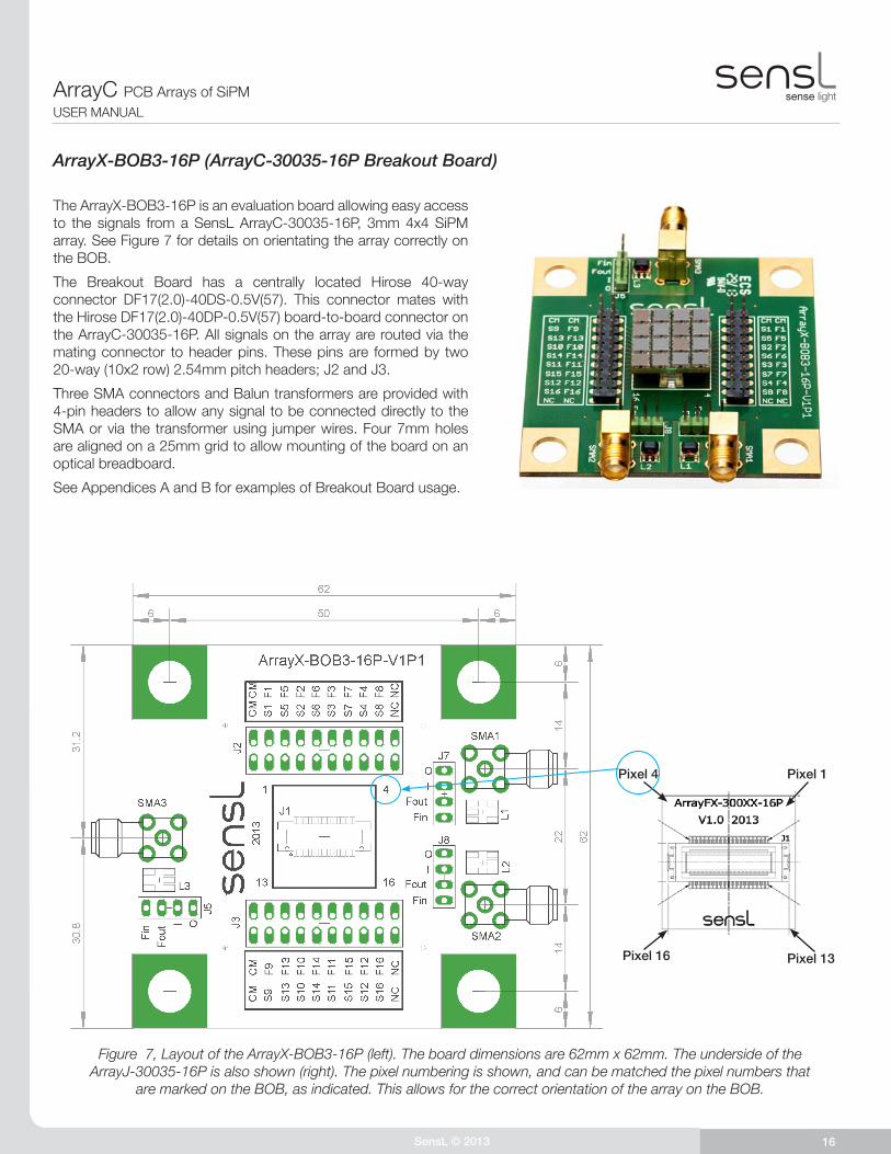
The ArrayX-BOB3-16P is an evaluation board allowing easy access to the signals from a SensL ArrayC-30035-16P, 3mm 4x4 SiPM array. See Figure 7 for details on orientating the array correctly on the BOB.
The Breakout Board has a centrally located Hirose 40-way connector DF17(2.0)-40DS-0.5V(57). This connector mates with the Hirose DF17(2.0)-40DP-0.5V(57) board-to-board connector on the ArrayC-30035-16P. All signals on the array are routed via the mating connector to header pins. These pins are formed by two 20-way (10x2 row) 2.54mm pitch headers; J2 and J3.
Three SMA connectors and Balun transformers are provided with 4-pin headers to allow any signal to be connected directly to the SMA or via the transformer using jumper wires. Four 7mm holes are aligned on a 25mm grid to allow mounting of the board on an optical breadboard.
See Appendices A and B for examples of Breakout Board usage.
Figure 7, Layout of the ArrayX-BOB3-16P (left). The board dimensions are 62mm x 62mm. The underside of the ArrayJ-30035-16P is also shown (right). The pixel numbering is shown, and can be matched the pixel numbers that
are marked on the BOB, as indicated. This allows for the correct orientation of the array on the BOB.
Pixel 4 Pixel 1
Pixel 16 Pixel 13
SensL © 2013 17
ArrayC PCB Arrays of SiPMUSER MANUAL
SensL © 2013 17
ArrayC PCB Arrays of SiPMUSER MANUAL
PIN J2 J3
1 2 CM CM CM CM
3 4 S1 F1 S9 F9
5 6 S5 F5 S13 F13
7 8 S2 F2 S10 F10
9 10 S6 F6 S14 F14
11 12 S3 F3 S11 F11
13 14 S7 F17 S15 F15
15 16 S4 F4 S12 F12
17 18 S8 F6 S16 F16
19 20 NC NC NC NC
Header Signals for the ArrayX-BOB3-16P
NC Not Connected
CM Common I/O
Sn Standard I/O of pixel n
Fn Fast output of pixel n
SensL © 2013 18
ArrayC PCB Arrays of SiPMUSER MANUAL
SensL © 2013 18
ArrayC PCB Arrays of SiPMUSER MANUAL
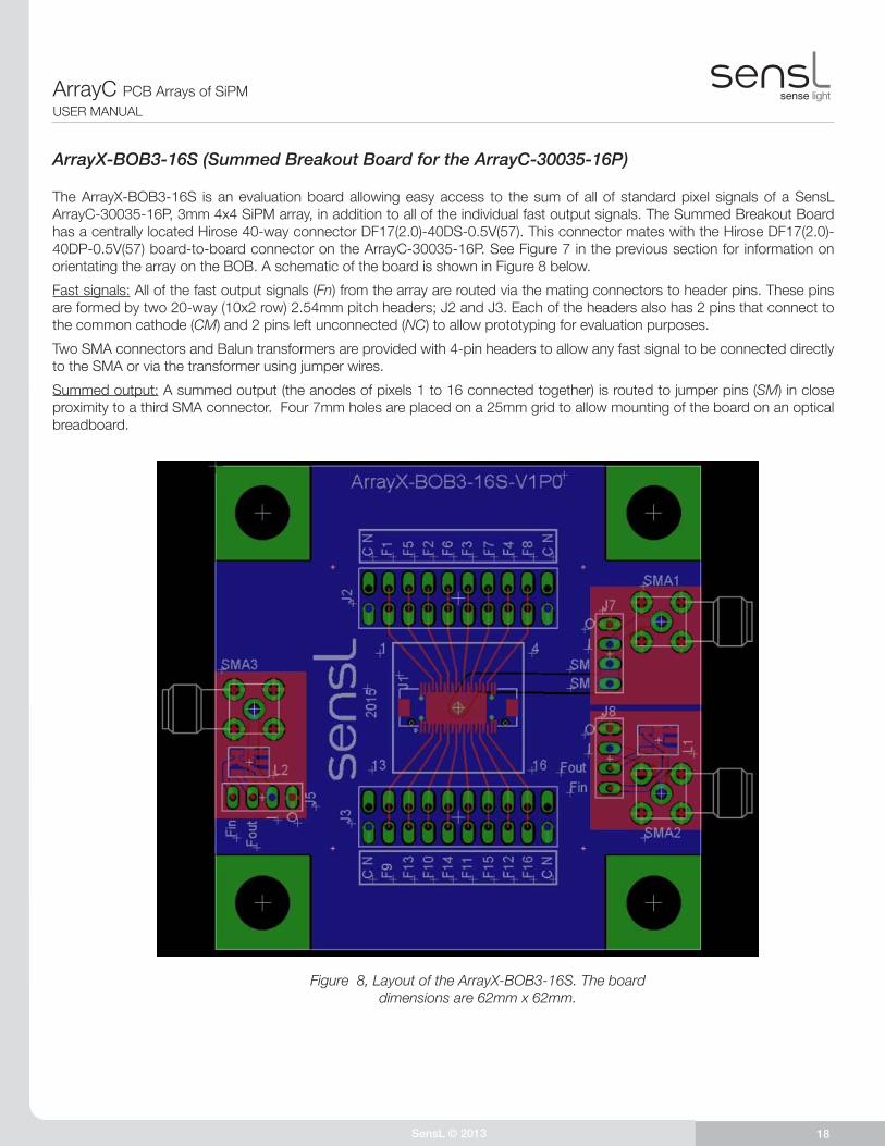
ArrayX-BOB3-16S (Summed Breakout Board for the ArrayC-30035-16P)
Figure 8, Layout of the ArrayX-BOB3-16S. The board dimensions are 62mm x 62mm.
The ArrayX-BOB3-16S is an evaluation board allowing easy access to the sum of all of standard pixel signals of a SensL ArrayC-30035-16P, 3mm 4x4 SiPM array, in addition to all of the individual fast output signals. The Summed Breakout Board has a centrally located Hirose 40-way connector DF17(2.0)-40DS-0.5V(57). This connector mates with the Hirose DF17(2.0)-40DP-0.5V(57) board-to-board connector on the ArrayC-30035-16P. See Figure 7 in the previous section for information on orientating the array on the BOB. A schematic of the board is shown in Figure 8 below.
Fast signals: All of the fast output signals (Fn) from the array are routed via the mating connectors to header pins. These pins are formed by two 20-way (10x2 row) 2.54mm pitch headers; J2 and J3. Each of the headers also has 2 pins that connect to the common cathode (CM) and 2 pins left unconnected (NC) to allow prototyping for evaluation purposes.
Two SMA connectors and Balun transformers are provided with 4-pin headers to allow any fast signal to be connected directly to the SMA or via the transformer using jumper wires.
Summed output: A summed output (the anodes of pixels 1 to 16 connected together) is routed to jumper pins (SM) in close proximity to a third SMA connector. Four 7mm holes are placed on a 25mm grid to allow mounting of the board on an optical breadboard.
SensL © 2013 19
ArrayC PCB Arrays of SiPMUSER MANUAL
SensL © 2013 19
ArrayC PCB Arrays of SiPMUSER MANUAL
PIN J2 J3
1 2 CM NC CM NC
3 4 F1 F1 F9 F9
5 6 F5 F5 F13 F13
7 8 F2 F2 F10 F10
9 10 F6 F6 F14 F14
11 12 F3 F3 F11 F11
13 14 F7 F7 F15 F15
15 16 F4 F4 F12 F12
17 18 F8 F8 F16 F16
19 20 CM NC CM NC
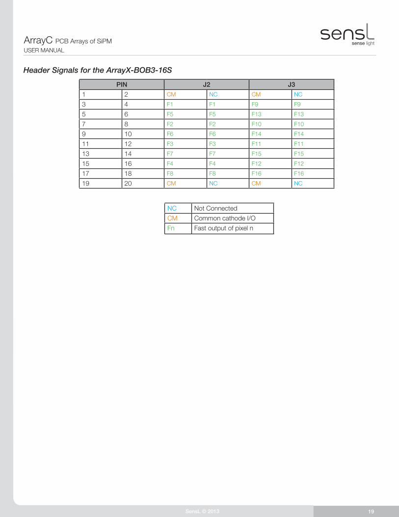
Header Signals for the ArrayX-BOB3-16S
NC Not Connected
CM Common cathode I/O
Fn Fast output of pixel n
SensL © 2013 20
ArrayC PCB Arrays of SiPMUSER MANUAL
SensL © 2013 20
ArrayC PCB Arrays of SiPMUSER MANUAL
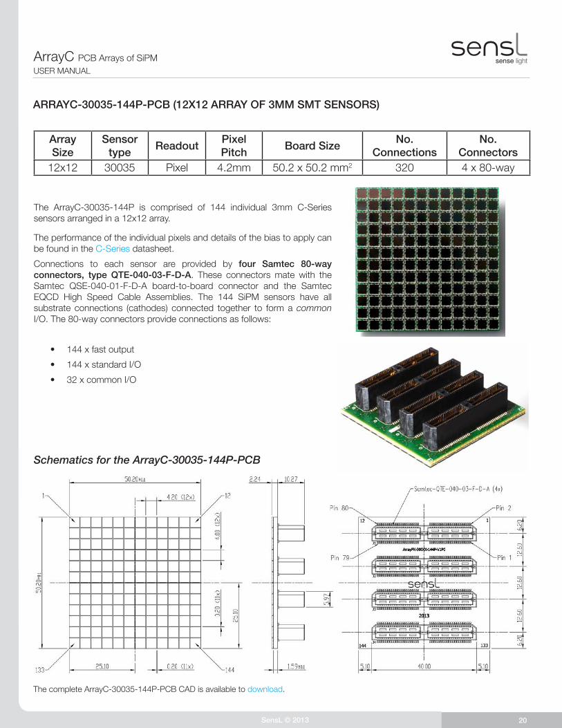
ARRAYC-30035-144P-PCB (12X12 ARRAY OF 3MM SMT SENSORS)
Array Size
Sensor type
ReadoutPixel Pitch
Board SizeNo.
ConnectionsNo.
Connectors12x12 30035 Pixel 4.2mm 50.2 x 50.2 mm2 320 4 x 80-way
The ArrayC-30035-144P is comprised of 144 individual 3mm C-Series sensors arranged in a 12x12 array.
The performance of the individual pixels and details of the bias to apply can be found in the C-Series datasheet.
Connections to each sensor are provided by four Samtec 80-way connectors, type QTE-040-03-F-D-A. These connectors mate with the Samtec QSE-040-01-F-D-A board-to-board connector and the Samtec EQCD High Speed Cable Assemblies. The 144 SiPM sensors have all substrate connections (cathodes) connected together to form a common I/O. The 80-way connectors provide connections as follows:
• 144 x fast output
• 144 x standard I/O
• 32 x common I/O
Schematics for the ArrayC-30035-144P-PCB
The complete ArrayC-30035-144P-PCB CAD is available to download.
SensL © 2013 21
ArrayC PCB Arrays of SiPMUSER MANUAL
SensL © 2013 21
ArrayC PCB Arrays of SiPMUSER MANUAL
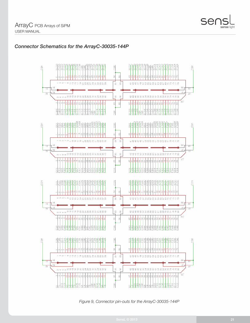
Connector Schematics for the ArrayC-30035-144P
Figure 9, Connector pin-outs for the ArrayC-30035-144P
SensL © 2013 22
ArrayC PCB Arrays of SiPMUSER MANUAL
SensL © 2013 22
ArrayC PCB Arrays of SiPMUSER MANUAL
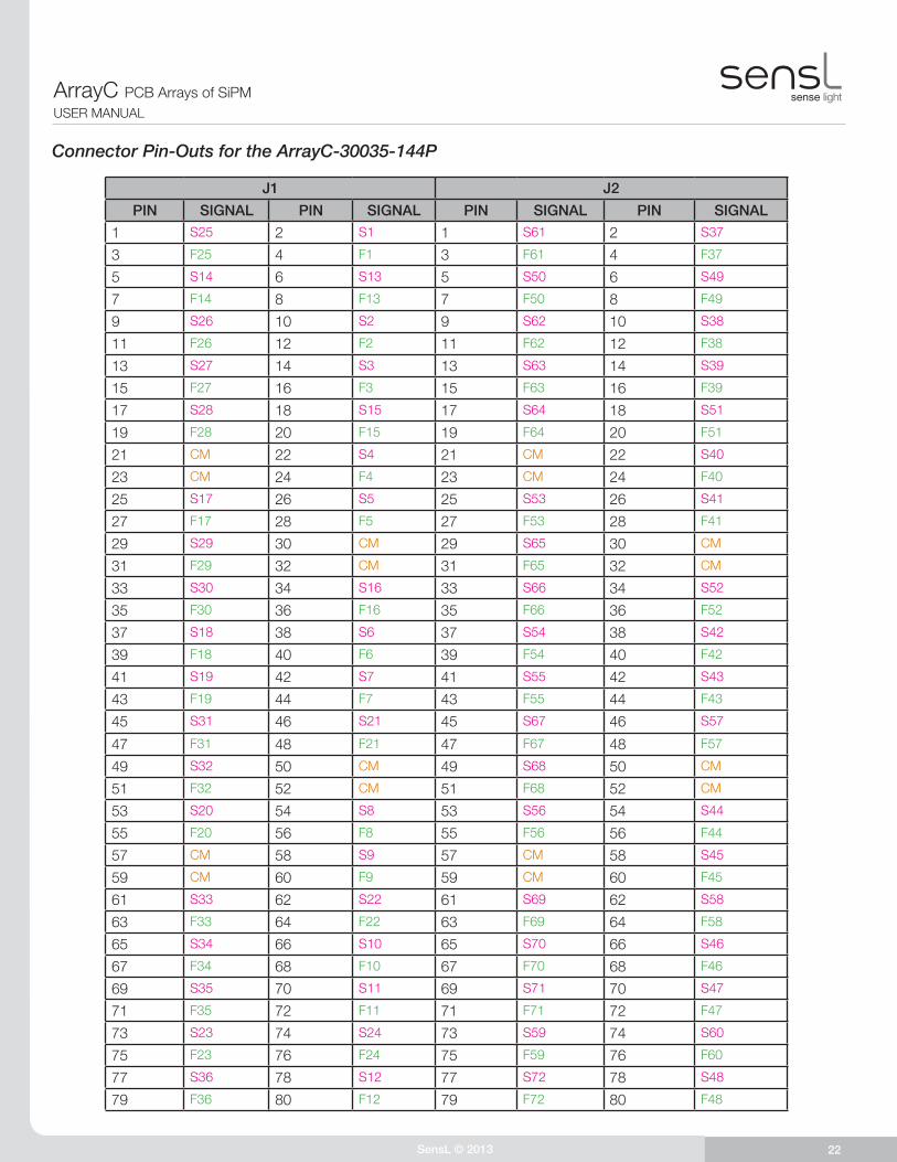
Connector Pin-Outs for the ArrayC-30035-144P
J1 J2
PIN SIGNAL PIN SIGNAL PIN SIGNAL PIN SIGNAL
1 S25 2 S1 1 S61 2 S37
3 F25 4 F1 3 F61 4 F37
5 S14 6 S13 5 S50 6 S49
7 F14 8 F13 7 F50 8 F49
9 S26 10 S2 9 S62 10 S38
11 F26 12 F2 11 F62 12 F38
13 S27 14 S3 13 S63 14 S39
15 F27 16 F3 15 F63 16 F39
17 S28 18 S15 17 S64 18 S51
19 F28 20 F15 19 F64 20 F51
21 CM 22 S4 21 CM 22 S40
23 CM 24 F4 23 CM 24 F40
25 S17 26 S5 25 S53 26 S41
27 F17 28 F5 27 F53 28 F41
29 S29 30 CM 29 S65 30 CM
31 F29 32 CM 31 F65 32 CM
33 S30 34 S16 33 S66 34 S52
35 F30 36 F16 35 F66 36 F52
37 S18 38 S6 37 S54 38 S42
39 F18 40 F6 39 F54 40 F42
41 S19 42 S7 41 S55 42 S43
43 F19 44 F7 43 F55 44 F43
45 S31 46 S21 45 S67 46 S57
47 F31 48 F21 47 F67 48 F57
49 S32 50 CM 49 S68 50 CM
51 F32 52 CM 51 F68 52 CM
53 S20 54 S8 53 S56 54 S44
55 F20 56 F8 55 F56 56 F44
57 CM 58 S9 57 CM 58 S45
59 CM 60 F9 59 CM 60 F45
61 S33 62 S22 61 S69 62 S58
63 F33 64 F22 63 F69 64 F58
65 S34 66 S10 65 S70 66 S46
67 F34 68 F10 67 F70 68 F46
69 S35 70 S11 69 S71 70 S47
71 F35 72 F11 71 F71 72 F47
73 S23 74 S24 73 S59 74 S60
75 F23 76 F24 75 F59 76 F60
77 S36 78 S12 77 S72 78 S48
79 F36 80 F12 79 F72 80 F48
SensL © 2013 23
ArrayC PCB Arrays of SiPMUSER MANUAL
SensL © 2013 23
ArrayC PCB Arrays of SiPMUSER MANUAL
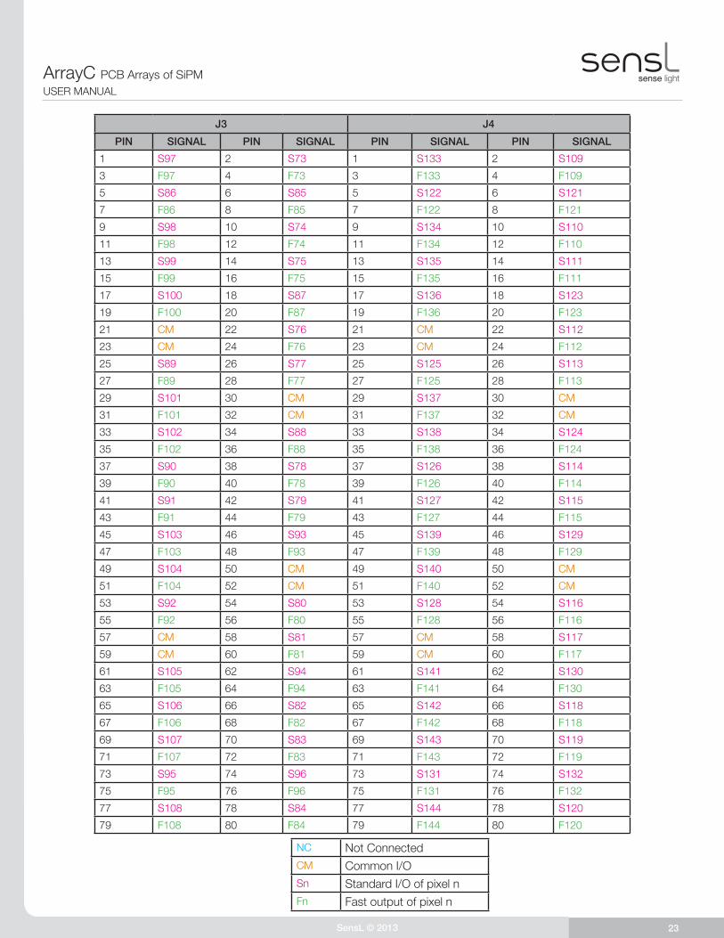
J3 J4
PIN SIGNAL PIN SIGNAL PIN SIGNAL PIN SIGNAL
1 S97 2 S73 1 S133 2 S109
3 F97 4 F73 3 F133 4 F109
5 S86 6 S85 5 S122 6 S121
7 F86 8 F85 7 F122 8 F121
9 S98 10 S74 9 S134 10 S110
11 F98 12 F74 11 F134 12 F110
13 S99 14 S75 13 S135 14 S111
15 F99 16 F75 15 F135 16 F111
17 S100 18 S87 17 S136 18 S123
19 F100 20 F87 19 F136 20 F123
21 CM 22 S76 21 CM 22 S112
23 CM 24 F76 23 CM 24 F112
25 S89 26 S77 25 S125 26 S113
27 F89 28 F77 27 F125 28 F113
29 S101 30 CM 29 S137 30 CM
31 F101 32 CM 31 F137 32 CM
33 S102 34 S88 33 S138 34 S124
35 F102 36 F88 35 F138 36 F124
37 S90 38 S78 37 S126 38 S114
39 F90 40 F78 39 F126 40 F114
41 S91 42 S79 41 S127 42 S115
43 F91 44 F79 43 F127 44 F115
45 S103 46 S93 45 S139 46 S129
47 F103 48 F93 47 F139 48 F129
49 S104 50 CM 49 S140 50 CM
51 F104 52 CM 51 F140 52 CM
53 S92 54 S80 53 S128 54 S116
55 F92 56 F80 55 F128 56 F116
57 CM 58 S81 57 CM 58 S117
59 CM 60 F81 59 CM 60 F117
61 S105 62 S94 61 S141 62 S130
63 F105 64 F94 63 F141 64 F130
65 S106 66 S82 65 S142 66 S118
67 F106 68 F82 67 F142 68 F118
69 S107 70 S83 69 S143 70 S119
71 F107 72 F83 71 F143 72 F119
73 S95 74 S96 73 S131 74 S132
75 F95 76 F96 75 F131 76 F132
77 S108 78 S84 77 S144 78 S120
79 F108 80 F84 79 F144 80 F120
NC Not ConnectedCM Common I/OSn Standard I/O of pixel nFn Fast output of pixel n
SensL © 2013 24
ArrayC PCB Arrays of SiPMUSER MANUAL
SensL © 2013 24
ArrayC PCB Arrays of SiPMUSER MANUAL
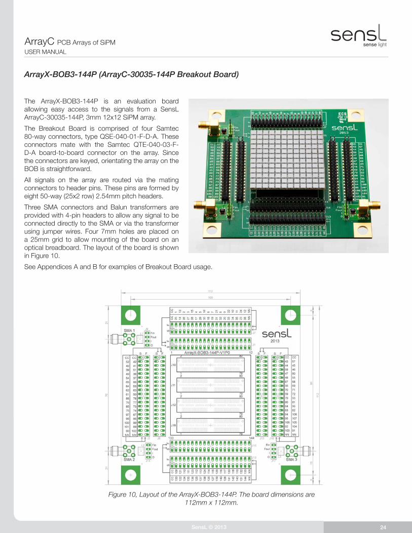
ArrayX-BOB3-144P (ArrayC-30035-144P Breakout Board)
The ArrayX-BOB3-144P is an evaluation board allowing easy access to the signals from a SensL ArrayC-30035-144P, 3mm 12x12 SiPM array.
The Breakout Board is comprised of four Samtec 80-way connectors, type QSE-040-01-F-D-A. These connectors mate with the Samtec QTE-040-03-F-D-A board-to-board connector on the array. Since the connectors are keyed, orientating the array on the BOB is straightforward.
All signals on the array are routed via the mating connectors to header pins. These pins are formed by eight 50-way (25x2 row) 2.54mm pitch headers.
Three SMA connectors and Balun transformers are provided with 4-pin headers to allow any signal to be connected directly to the SMA or via the transformer using jumper wires. Four 7mm holes are placed on a 25mm grid to allow mounting of the board on an optical breadboard. The layout of the board is shown in Figure 10.
See Appendices A and B for examples of Breakout Board usage.
Figure 10, Layout of the ArrayX-BOB3-144P. The board dimensions are 112mm x 112mm.
SensL © 2013 25
ArrayC PCB Arrays of SiPMUSER MANUAL
SensL © 2013 25
ArrayC PCB Arrays of SiPMUSER MANUAL
PIN J1 J2 J7 J8
1 2 CM CM CM CM CM CM CM CM
3 4 S25 F25 S52 F52 S1 F1 S42 F42
5 6 S14 F14 S40 F40 S13 F13 S41 F41
7 8 S26 F26 S39 F39 S2 F2 S51 F51
9 10 S27 F27 S49 F49 S3 F3 S38 F38
11 12 S28 F28 S54 F54 S15 F15 S37 F37
13 14 S17 F17 S65 F65 S4 F4 S66 F66
15 16 S29 F29 S64 F64 S5 F5 S53 F53
17 18 S30 F30 S62 F62 S16 F16 S63 F63
19 20 S18 F18 S61 F61 S6 F6 S50 F50
21 22 S19 F19 S88 F88 S7 F7 S78 F78
23 24 S31 F31 S76 F76 S21 F21 S77 F77
25 26 S32 F32 S85 F85 S8 F8 S73 F73
27 28 S20 F20 S75 F75 S9 F9 S74 F74
29 30 S33 F33 S97 F97 S22 F22 S87 F87
31 32 S34 F34 S98 F98 S10 F10 S86 F86
33 34 S35 F35 S100 F100 S11 F11 S99 F99
35 36 S23 F23 S101 F101 S24 F24 S89 F89
37 38 S36 F36 S90 F90 S12 F12 S102 F102
39 40 NC NC NC NC NC NC NC NC
PIN J13 J15 J16 J18
1 2 CM CM CM CM CM CM CM CM
3 4 S133 F133 S43 F43 S109 F109 S57 F57
5 6 S122 F122 S44 F44 S121 F121 S45 F45
7 8 S134 F134 S58 F58 S110 F110 S46 F46
9 10 S135 F135 S47 F47 S111 F111 S60 F60
11 12 S136 F136 S48 F48 S123 F123 S55 F55
13 14 S125 F125 S67 F67 S112 F112 S68 F68
15 16 S137 F137 S56 F56 S113 F113 S69 F69
17 18 S138 F138 S70 F70 S124 F124 S71 F71
19 20 S126 F126 S59 F59 S114 F114 S72 F72
21 22 S127 F127 S79 F79 S115 F115 S93 F93
23 24 S139 F139 S80 F80 S129 F129 S81 F81
25 26 S140 F140 S84 F84 S116 F116 S96 F96
27 28 S128 F128 S83 F83 S117 F117 S82 F82
29 30 S141 F141 S94 F94 S130 F130 S108 F108
31 32 S142 F142 S95 F95 S118 F118 S107 F107
33 34 S143 F143 S106 F106 S119 F119 S105 F105
35 36 S131 F131 S92 F92 S132 F132 S104 F104
37 38 S144 F144 S103 F103 S120 F120 S91 F91
39 40 NC NC NC NC NC NC NC NC
Header Signals for the ArrayX-BOB3-144P
NC Not Connected Sn Standard I/O of pixel nCM Common I/O Fn Fast output of pixel n
SensL © 2013 26
ArrayC PCB Arrays of SiPMUSER MANUAL
SensL © 2013 26
ArrayC PCB Arrays of SiPMUSER MANUAL
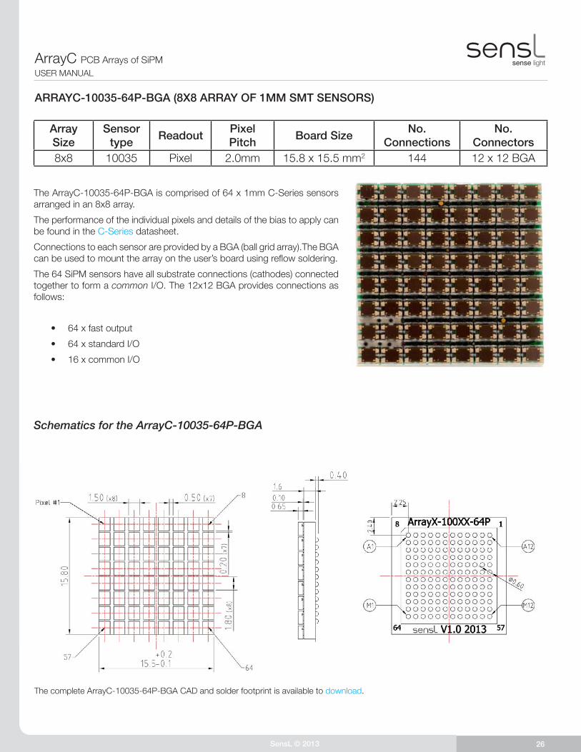
ARRAYC-10035-64P-BGA (8X8 ARRAY OF 1MM SMT SENSORS)
Array Size
Sensor type
ReadoutPixel Pitch
Board SizeNo.
ConnectionsNo.
Connectors8x8 10035 Pixel 2.0mm 15.8 x 15.5 mm2 144 12 x 12 BGA
The ArrayC-10035-64P-BGA is comprised of 64 x 1mm C-Series sensors arranged in an 8x8 array.
The performance of the individual pixels and details of the bias to apply can be found in the C-Series datasheet.
Connections to each sensor are provided by a BGA (ball grid array).The BGA can be used to mount the array on the user’s board using reflow soldering.
The 64 SiPM sensors have all substrate connections (cathodes) connected together to form a common I/O. The 12x12 BGA provides connections as follows:
• 64 x fast output
• 64 x standard I/O
• 16 x common I/O
Schematics for the ArrayC-10035-64P-BGA
The complete ArrayC-10035-64P-BGA CAD and solder footprint is available to download.
SensL © 2013 27
ArrayC PCB Arrays of SiPMUSER MANUAL
SensL © 2013 27
ArrayC PCB Arrays of SiPMUSER MANUAL
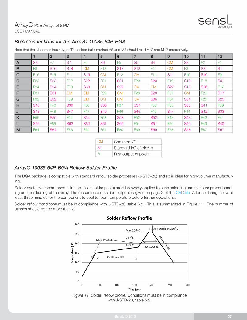
1 2 3 4 5 6 7 8 9 10 11 12
A S8 F7 S7 F6 S6 F5 S5 S4 CM S3 F2 F1
B F8 S16 S14 CM F13 S13 S12 F4 CM F3 S2 S1
C F16 F15 F14 S15 CM F12 CM F11 S11 F10 S10 F9
D F23 S23 F22 S22 F21 S21 F20 S20 F19 S19 F18 S9
E F24 S24 F30 S30 CM S29 CM CM S27 S18 S26 F17
F F31 S31 CM CM F29 CM F28 S28 F27 CM F26 S17
G F32 S32 F39 CM CM CM CM S36 F34 S34 F25 S25
H S40 F40 S39 F38 S38 F37 S37 F36 F35 S35 S41 F33
J S48 F48 S47 F47 S46 F46 S45 F45 S44 F44 S42 S33
K F56 S55 F54 S54 F53 S53 F52 S52 F43 S43 F42 F41
L S56 F55 S63 S62 S61 S60 F51 S51 F50 S50 F49 S49
M F64 S64 F63 F62 F61 F60 F59 S59 F58 S58 F57 S57
BGA Connections for the ArrayC-10035-64P-BGA
CM Common I/OSn Standard I/O of pixel nFn Fast output of pixel n
ArrayC-10035-64P-BGA Reflow Solder Profile
The BGA package is compatible with standard reflow solder processes (J-STD-20) and so is ideal for high-volume manufactur-ing.
Solder paste (we recommend using no-clean solder paste) must be evenly applied to each soldering pad to insure proper bond-ing and positioning of the array. The reccomended solder footprint is given on page 2 of the CAD file. After soldering, allow at least three minutes for the component to cool to room temperature before further operations.
Solder reflow conditions must be in compliance with J-STD-20, table 5.2. This is summarized in Figure 11. The number of passes should not be more than 2.
0
50
100
150
200
250
300
0 50 100 150 200 250 300
Tem
pera
ture
(OC)
Time (sec)
Solder Reflow Profile
Max 4OC/sec
60 to 120 sec
Max 260OC
217OC
180OC 60~100sec
Max 10sec at 260OC
Figure 11, Solder reflow profile. Conditions must be in compliance with J-STD-20, table 5.2.
Note that the silkscreen has a typo. The solder balls marked A8 and M8 should read A12 and M12 respectively.
SensL © 2013 28
ArrayC PCB Arrays of SiPMUSER MANUAL
SensL © 2013 28
ArrayC PCB Arrays of SiPMUSER MANUAL
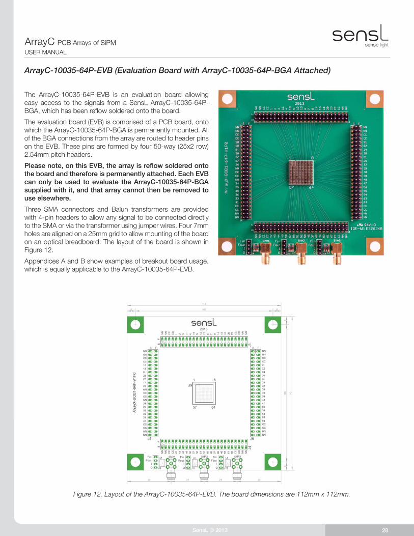
ArrayC-10035-64P-EVB (Evaluation Board with ArrayC-10035-64P-BGA Attached)
The ArrayC-10035-64P-EVB is an evaluation board allowing easy access to the signals from a SensL ArrayC-10035-64P-BGA, which has been reflow soldered onto the board.
The evaluation board (EVB) is comprised of a PCB board, onto which the ArrayC-10035-64P-BGA is permanently mounted. All of the BGA connections from the array are routed to header pins on the EVB. These pins are formed by four 50-way (25x2 row) 2.54mm pitch headers.
Please note, on this EVB, the array is reflow soldered onto the board and therefore is permanently attached. Each EVB can only be used to evaluate the ArrayC-10035-64P-BGA supplied with it, and that array cannot then be removed to use elsewhere.
Three SMA connectors and Balun transformers are provided with 4-pin headers to allow any signal to be connected directly to the SMA or via the transformer using jumper wires. Four 7mm holes are aligned on a 25mm grid to allow mounting of the board on an optical breadboard. The layout of the board is shown in Figure 12.
Appendices A and B show examples of breakout board usage, which is equally applicable to the ArrayC-10035-64P-EVB.
Figure 12, Layout of the ArrayC-10035-64P-EVB. The board dimensions are 112mm x 112mm.
SensL © 2013 29
ArrayC PCB Arrays of SiPMUSER MANUAL
SensL © 2013 29
ArrayC PCB Arrays of SiPMUSER MANUAL
PIN J3 J4 J5 J6
1 2 NC NC NC NC NC NC NC NC
3 4 NC NC NC NC NC NC NC NC
5 6 CM CM CM CM CM CM CM CM
7 8 CM CM CM CM CM CM CM CM
9 10 S1 F1 S42 F42 S10 F10 S21 F21
11 12 S2 F2 S43 F43 S18 F18 S22 F22
13 14 S3 F3 S44 F44 S9 F9 S24 F24
15 16 S11 F11 S49 F49 S28 F28 S30 F30
17 18 S4 F4 S50 F50 S27 F27 S31 F31
19 20 S19 F19 S57 F57 S17 F17 S29 F29
21 22 S5 F5 S58 F58 S26 F26 S32 F32
23 24 S12 F12 S51 F51 NC NC S39 F39
25 26 S13 F13 S52 F52 CM CM S40 F40
27 28 S6 F6 S59 F59 CM CM S38 F38
29 30 S7 F7 S45 F45 NC NC S48 F48
31 32 S8 F8 S37 F37 S34 F34 S47 F47
33 34 S14 F14 S60 F60 S25 F25 S56 F56
35 36 S15 F15 S46 F46 S35 F35 S55 F55
37 38 S16 F16 S53 F53 S36 F36 S54 F54
39 40 S20 F20 S61 F61 S33 F33 S63 F63
41 42 S23 F23 S62 F62 S41 F41 S64 F64
43 44 CM CM CM CM CM CM CM CM
45 46 CM CM CM CM CM CM CM CM
47 48 NC NC NC NC NC NC NC NC
49 50 NC NC NC NC NC NC NC NC
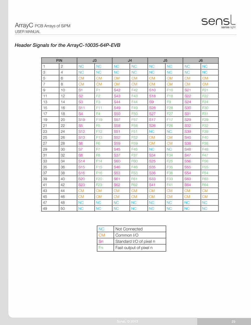
Header Signals for the ArrayC-10035-64P-EVB
NC Not Connected
CM Common I/O
Sn Standard I/O of pixel n
Fn Fast output of pixel n
SensL © 2013 30
ArrayC PCB Arrays of SiPMUSER MANUAL
SensL © 2013 30
ArrayC PCB Arrays of SiPMUSER MANUAL
BIASING AND READOUT FROM THE STANDARD BREAKOUT BOARDS *
The purpose of the Breakout Boards is to allow easy access to either standard or fast I/O from individual pixels for testing purposes. It should be stressed that the breakout boards are for evaluation purposes only and do not allow for full readout of all pixels simultaneously.
The various Breakout Boards described in this document have features in common. All pixel fast and standard signals are brought out to headers. The header pins can be interfaced with the SMA connectors with the option of routing the signal via a balun transformer. The common I/O consists of all of the substrate connections summed together. It is not recommended to apply the bias to the common I/O.
The Breakout Boards are each shipped with 3 x shunt jumpers and 6 x 10cm wire cables (3 x red, 3 x black) with crimp sockets at each end.
All header pins are suitable for use with wire wrapping in addition to the jumpers and crimp socket leads supplied.
The ‘NC’ signals are unconnected pins that can be used for prototyping.
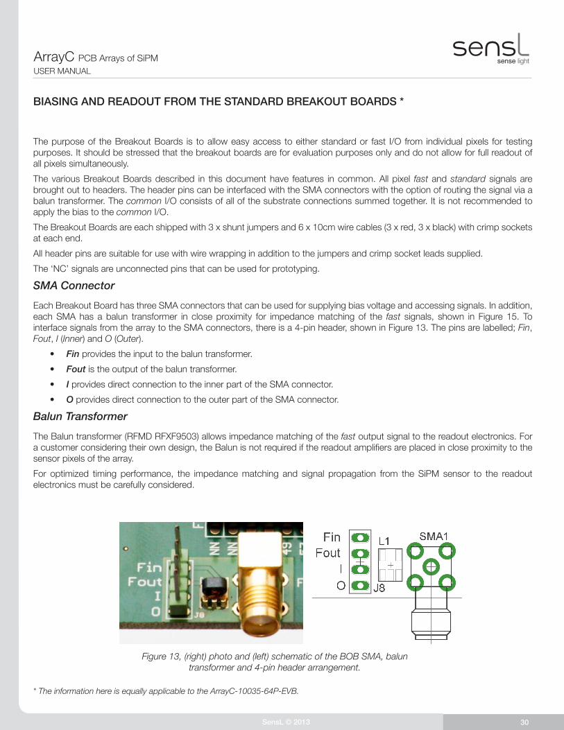
SMA Connector
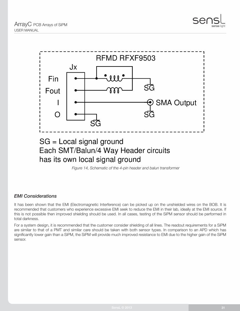
Each Breakout Board has three SMA connectors that can be used for supplying bias voltage and accessing signals. In addition, each SMA has a balun transformer in close proximity for impedance matching of the fast signals, shown in Figure 15. To interface signals from the array to the SMA connectors, there is a 4-pin header, shown in Figure 13. The pins are labelled; Fin, Fout, I (Inner) and O (Outer).
• Fin provides the input to the balun transformer.
• Fout is the output of the balun transformer.
• I provides direct connection to the inner part of the SMA connector.
• O provides direct connection to the outer part of the SMA connector.
Balun Transformer
The Balun transformer (RFMD RFXF9503) allows impedance matching of the fast output signal to the readout electronics. For a customer considering their own design, the Balun is not required if the readout amplifiers are placed in close proximity to the sensor pixels of the array.
For optimized timing performance, the impedance matching and signal propagation from the SiPM sensor to the readout electronics must be carefully considered.
* The information here is equally applicable to the ArrayC-10035-64P-EVB.
Figure 13, (right) photo and (left) schematic of the BOB SMA, balun transformer and 4-pin header arrangement.
SensL © 2013 31
ArrayC PCB Arrays of SiPMUSER MANUAL
SensL © 2013 31
ArrayC PCB Arrays of SiPMUSER MANUAL
EMI Considerations
It has been shown that the EMI (Electromagnetic Interference) can be picked up on the unshielded wires on the BOB. It is recommended that customers who experience excessive EMI seek to reduce the EMI in their lab, ideally at the EMI source. If this is not possible then improved shielding should be used. In all cases, testing of the SiPM sensor should be performed in total darkness.
For a system design, it is recommended that the customer consider shielding of all lines. The readout requirements for a SiPM are similar to that of a PMT and similar care should be taken with both sensor types. In comparison to an APD which has significantly lower gain than a SiPM, the SiPM will provide much improved resistance to EMI due to the higher gain of the SiPM sensor.
Figure 14, Schematic of the 4-pin header and balun transformer
SensL © 2013 32
ArrayC PCB Arrays of SiPMUSER MANUAL
SensL © 2013 32
ArrayC PCB Arrays of SiPMUSER MANUAL
APPENDIX A - EXAMPLE OF USING THE BREAKOUT BOARD TO READOUT FAST SIGNALS
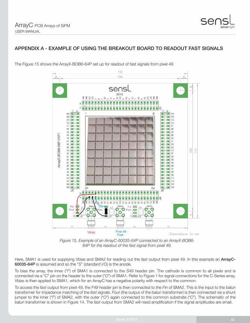
The Figure 15 shows the ArrayX-BOB6-64P set up for readout of fast signals from pixel 49
Here, SMA1 is used for supplying Vbias and SMA2 for reading out the fast output from pixel 49. In this example an ArrayC-60035-64P is assumed and so the “S” (standard I/O) is the anode.
To bias the array, the inner (“I”) of SMA1 is connected to the S49 header pin. The cathode is common to all pixels and is connected via a “C” pin on the header to the outer (“O”) of SMA1. Refer to Figure 1 for signal connections for the C-Series array. Vbias is then applied to SMA1, which for an ArrayC has a negative polarity with respect to the common.
To access the fast output from pixel 49, the F49 header pin is then connected to the Fin of SMA2. This is the input to the balun transformer for impedance matching of the fast signals. Fout (the output of the balun transformer) is then connected via a shunt jumper to the inner (“I”) of SMA2, with the outer (“O”) again connected to the common substrate (“C”). The schematic of the balun transformer is shown in Figure 14. The fast output from SMA2 will need amplification if the signal amplitudes are small.
Figure 15, Example of an ArrayC-60035-64P connected to an ArrayX-BOB6-64P for the readout of the fast signal from pixel 49.
SensL © 2013 33
ArrayC PCB Arrays of SiPMUSER MANUAL
SensL © 2013 33
ArrayC PCB Arrays of SiPMUSER MANUAL
APPENDIX B - EXAMPLE OF USING THE BREAKOUT BOARD TO READOUT STANDARD SIGNALS
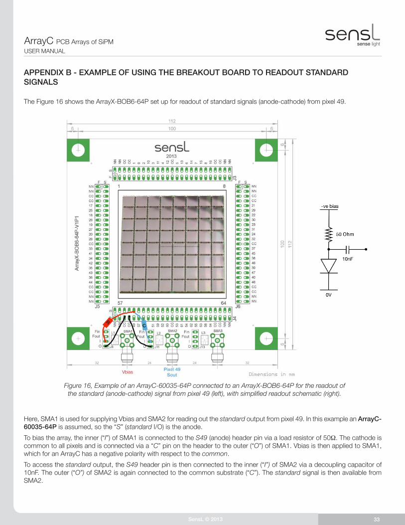
The Figure 16 shows the ArrayX-BOB6-64P set up for readout of standard signals (anode-cathode) from pixel 49.
Here, SMA1 is used for supplying Vbias and SMA2 for reading out the standard output from pixel 49. In this example an ArrayC-60035-64P is assumed, so the “S” (standard I/O) is the anode.
To bias the array, the inner (“I”) of SMA1 is connected to the S49 (anode) header pin via a load resistor of 50W. The cathode is common to all pixels and is connected via a “C” pin on the header to the outer (“O”) of SMA1. Vbias is then applied to SMA1, which for an ArrayC has a negative polarity with respect to the common.
To access the standard output, the S49 header pin is then connected to the inner (“I”) of SMA2 via a decoupling capacitor of 10nF. The outer (“O”) of SMA2 is again connected to the common substrate (“C”). The standard signal is then available from SMA2.
Figure 16, Example of an ArrayC-60035-64P connected to an ArrayX-BOB6-64P for the readout of the standard (anode-cathode) signal from pixel 49 (left), with simplified readout schematic (right).
SensL © 2013 34
ArrayC PCB Arrays of SiPMUSER MANUAL
SensL © 2013 34
ArrayC PCB Arrays of SiPMUSER MANUAL
APPENDIX C - EXAMPLE OF USING THE SUMMED BREAKOUT BOARD
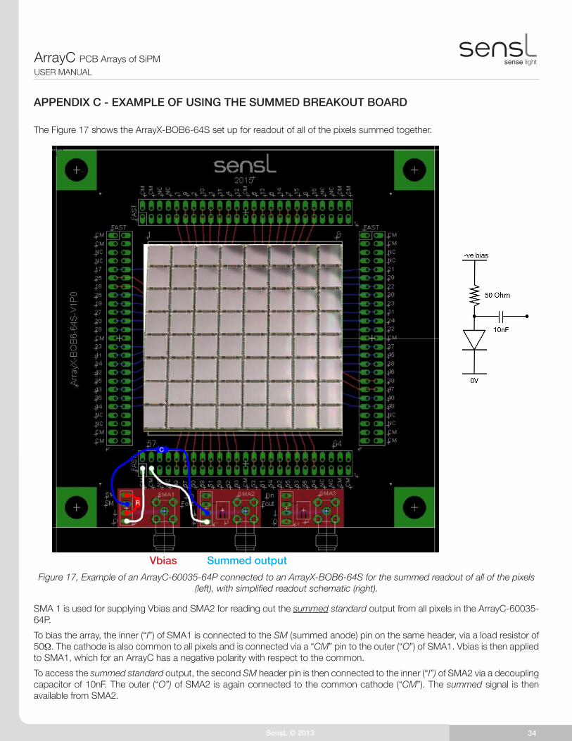
The Figure 17 shows the ArrayX-BOB6-64S set up for readout of all of the pixels summed together.
SMA 1 is used for supplying Vbias and SMA2 for reading out the summed standard output from all pixels in the ArrayC-60035-64P.
To bias the array, the inner (“I”) of SMA1 is connected to the SM (summed anode) pin on the same header, via a load resistor of 50W. The cathode is also common to all pixels and is connected via a “CM” pin to the outer (“O”) of SMA1. Vbias is then applied to SMA1, which for an ArrayC has a negative polarity with respect to the common.
To access the summed standard output, the second SM header pin is then connected to the inner (“I”) of SMA2 via a decoupling capacitor of 10nF. The outer (“O”) of SMA2 is again connected to the common cathode (“CM”). The summed signal is then available from SMA2.
Figure 17, Example of an ArrayC-60035-64P connected to an ArrayX-BOB6-64S for the summed readout of all of the pixels (left), with simplified readout schematic (right).
Summed outputVbias
SensL © 2013 35
ArrayC PCB Arrays of SiPMUSER MANUAL
SensL © 2013 35
ArrayC PCB Arrays of SiPMUSER MANUAL
Rev. 3.4, Preliminary, October 2017
+353 21 240 7110 (International)+1 650 641 3278 (North America)
SensL © 2013 35
All specifications are subject to change without notice
ArrayC PCB Arrays of SiPMUSER MANUAL
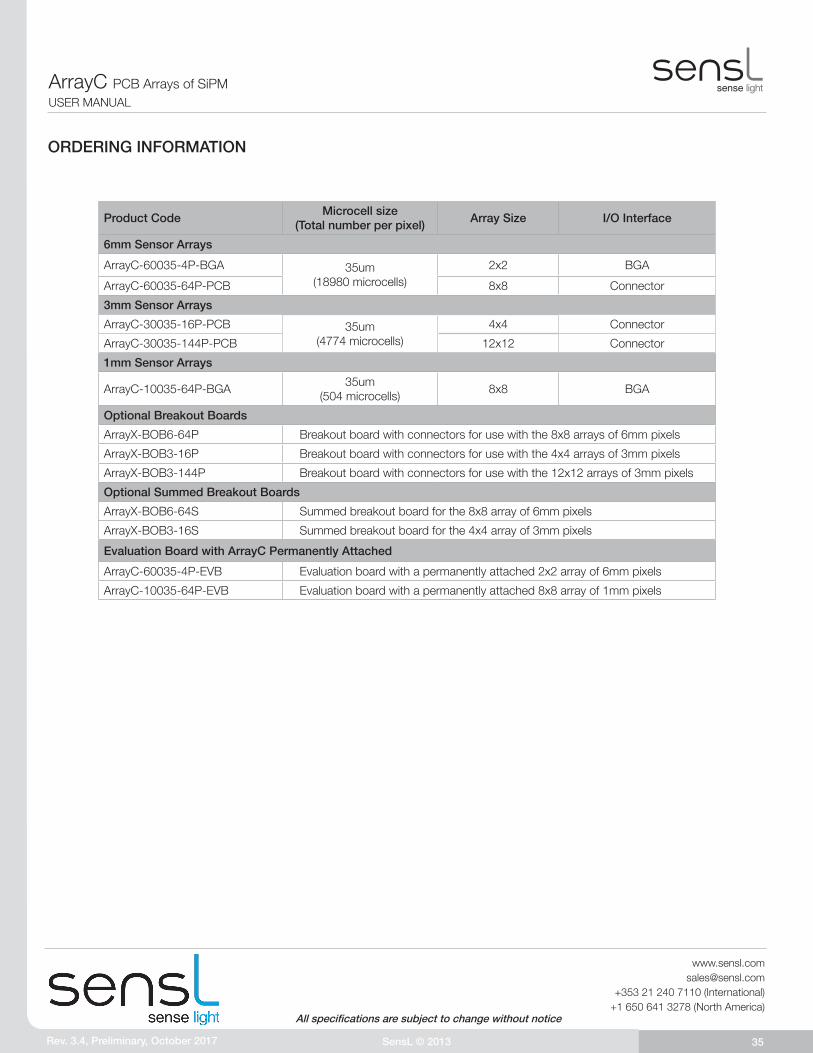
ORDERING INFORMATION
Product CodeMicrocell size
(Total number per pixel)Array Size I/O Interface
6mm Sensor Arrays
ArrayC-60035-4P-BGA 35um(18980 microcells)
2x2 BGA
ArrayC-60035-64P-PCB 8x8 Connector
3mm Sensor Arrays
ArrayC-30035-16P-PCB 35um(4774 microcells)
4x4 Connector
ArrayC-30035-144P-PCB 12x12 Connector
1mm Sensor Arrays
ArrayC-10035-64P-BGA35um
(504 microcells)8x8 BGA
Optional Breakout Boards
ArrayX-BOB6-64P Breakout board with connectors for use with the 8x8 arrays of 6mm pixels
ArrayX-BOB3-16P Breakout board with connectors for use with the 4x4 arrays of 3mm pixels
ArrayX-BOB3-144P Breakout board with connectors for use with the 12x12 arrays of 3mm pixels
Optional Summed Breakout Boards
ArrayX-BOB6-64S Summed breakout board for the 8x8 array of 6mm pixels
ArrayX-BOB3-16S Summed breakout board for the 4x4 array of 3mm pixels
Evaluation Board with ArrayC Permanently Attached
ArrayC-60035-4P-EVB Evaluation board with a permanently attached 2x2 array of 6mm pixels
ArrayC-10035-64P-EVB Evaluation board with a permanently attached 8x8 array of 1mm pixels